diff options
194 files changed, 73324 insertions, 1 deletions
diff --git a/build_keyboard.mk b/build_keyboard.mk index 9f6c42ea1..a73741bb3 100644 --- a/build_keyboard.mk +++ b/build_keyboard.mk @@ -144,6 +144,9 @@ endif ifdef MCU_FAMILY FIRMWARE_FORMAT?=bin PLATFORM=CHIBIOS +else ifdef ARM_ATSAM + PLATFORM=ARM_ATSAM + FIRMWARE_FORMAT=bin else PLATFORM=AVR FIRMWARE_FORMAT?=hex @@ -286,6 +289,11 @@ endif include $(TMK_PATH)/avr.mk endif +ifeq ($(PLATFORM),ARM_ATSAM) + include $(TMK_PATH)/arm_atsam.mk + include $(TMK_PATH)/protocol/arm_atsam.mk +endif + ifeq ($(PLATFORM),CHIBIOS) include $(TMK_PATH)/protocol/chibios.mk endif diff --git a/keyboards/alt67/alt67.h b/keyboards/alt67/alt67.h new file mode 100644 index 000000000..387985512 --- /dev/null +++ b/keyboards/alt67/alt67.h @@ -0,0 +1,24 @@ +#pragma once + +#include "quantum.h" +#include "config_led.h" +#include "matrix.h" + +#include "i2c_master.h" +#include "led_matrix.h" //For led keycodes +#include "usb/udi_cdc.h" +#include "usb/usb2422.h" + +#define LAYOUT( \ + K01, K02, K03, K04, K05, K06, K07, K08, K09, K10, K11, K12, K13, K14, K15, \ + K16, K17, K18, K19, K20, K21, K22, K23, K24, K25, K26, K27, K28, K29, K30, \ + K31, K32, K33, K34, K35, K36, K37, K38, K39, K40, K41, K42, K43, K44, K45, \ + K46, K47, K48, K49, K50, K51, K52, K53, K54, K55, K56, K57, K58, K59, K60, \ + K61, K62, K63, K64, K65, K66, K67 \ +) { \ + { K01, K02, K03, K04, K05, K06, K07, K08, K09, K10, K11, K12, K13, K14, K15, }, \ + { K16, K17, K18, K19, K20, K21, K22, K23, K24, K25, K26, K27, K28, K29, K30, }, \ + { K31, K32, K33, K34, K35, K36, K37, K38, K39, K40, K41, K42, KC_NO, K43, K44, }, \ + { K45, KC_NO, K46, K47, K48, K49, K50, K51, K52, K53, K54, K55, K56, K57, K58, }, \ + { K59, K60, K61, KC_NO, KC_NO, KC_NO, K62, KC_NO, KC_NO, KC_NO, K63, K64, K65, K66, K67, }, \ +} diff --git a/keyboards/alt67/config.h b/keyboards/alt67/config.h new file mode 100644 index 000000000..c67ae7d43 --- /dev/null +++ b/keyboards/alt67/config.h @@ -0,0 +1,79 @@ +/* +Copyright 2015 Jun Wako <wakojun@gmail.com> + +This program is free software: you can redistribute it and/or modify +it under the terms of the GNU General Public License as published by +the Free Software Foundation, either version 2 of the License, or +(at your option) any later version. + +This program is distributed in the hope that it will be useful, +but WITHOUT ANY WARRANTY; without even the implied warranty of +MERCHANTABILITY or FITNESS FOR A PARTICULAR PURPOSE. See the +GNU General Public License for more details. + +You should have received a copy of the GNU General Public License +along with this program. If not, see <http://www.gnu.org/licenses/>. +*/ + +#pragma once + +#include "config_common.h" + +/* USB Device descriptor parameter */ +#define VENDOR_ID 0x04D8 +#define PRODUCT_ID 0xEED3 +#define DEVICE_VER 0x0101 + +#define MANUFACTURER "Massdrop Inc." +#define PRODUCT "ALT67 Keyboard" +#define SERIAL_NUM "Unavailable" + +/* key matrix size */ +#define MATRIX_ROWS 5 +#define MATRIX_COLS 15 + +#define PA 0 +#define PB 1 + +#define MATRIX_ROW_PORTS PA, PA, PA, PA, PA +#define MATRIX_ROW_PINS 0, 1, 2, 3, 4 + +#define MATRIX_COL_PORTS PB, PB, PB, PB, PB, PB, PB, PB, PB, PB, PA, PA, PA, PA, PA +#define MATRIX_COL_PINS 4, 5, 6, 7, 8, 9, 10, 11, 12, 13, 5, 6, 7, 10, 11 + +/* Print boot debug codes using debug LED when M28 and M30 shorted */ +#define DEBUG_BOOT_TRACING + +/* Debounce reduces chatter (unintended double-presses) - set 0 if debouncing is not needed */ +#define DEBOUNCING_DELAY 5 + +/* Mechanical locking support. Use KC_LCAP, KC_LNUM or KC_LSCR instead in keymap */ +//#define LOCKING_SUPPORT_ENABLE +/* Locking resynchronize hack */ +//#define LOCKING_RESYNC_ENABLE + +/* key combination for command */ +#define IS_COMMAND() ( \ + keyboard_report->mods == (MOD_BIT(KC_LSHIFT) | MOD_BIT(KC_RSHIFT)) \ +) + +/* Force boot in NKRO mode */ +//#define FORCE_NKRO + +/* + * Feature disable options + * These options are also useful to firmware size reduction. + */ + +/* disable debug print */ +//#define NO_DEBUG + +/* disable print */ +//#define NO_PRINT + +/* disable action features */ +//#define NO_ACTION_LAYER +//#define NO_ACTION_TAPPING +//#define NO_ACTION_ONESHOT +//#define NO_ACTION_MACRO +//#define NO_ACTION_FUNCTION diff --git a/keyboards/alt67/config_led.h b/keyboards/alt67/config_led.h new file mode 100644 index 000000000..a049e3817 --- /dev/null +++ b/keyboards/alt67/config_led.h @@ -0,0 +1,178 @@ +/* +Copyright 2018 Massdrop Inc. + +This program is free software: you can redistribute it and/or modify +it under the terms of the GNU General Public License as published by +the Free Software Foundation, either version 2 of the License, or +(at your option) any later version. + +This program is distributed in the hope that it will be useful, +but WITHOUT ANY WARRANTY; without even the implied warranty of +MERCHANTABILITY or FITNESS FOR A PARTICULAR PURPOSE. See the +GNU General Public License for more details. + +You should have received a copy of the GNU General Public License +along with this program. If not, see <http://www.gnu.org/licenses/>. +*/ + +#ifndef _config_led_h_ +#define _config_led_h_ + +//Define number of ISSI3733 drivers being used (1...16) +#define ISSI3733_DRIVER_COUNT 2 + +//Hardware address of each driver (Refer to ISSI3733 pdf "Table 1 Slave Address" and keyboard schematic) +#define ISSI3773_DRIVER_ADDRESSES { 0xA0, 0xBE } + +//LED I2C bus speed +#define I2C_HZ 580000 + +//Count of LED bodies +#define ISSI3733_LED_COUNT 105 + +//Default Global Current Register value (Default brightness 0 - 255) +#define ISSI3733_GCR_DEFAULT 128 + +#define LED_GCR_MAX 165 //Max GCR value (0 - 255) WARNING: Raising this value may overload the LED drivers and USB bus +#define LED_GCR_STEP 10 //GCR increment/decrement value + +//Automatic power rollback and recovery +#define V5_HIGH 2540 //5V high level (After low power detect, point at which LEDs are allowed to use more power ) +#define V5_LOW 2480 //5V low level (LED power rolled back to stay above this limit) +#define V5_CAT 2200 //5V catastrophic level (Host USB port potential to shut down) + +#define ANIMATION_SPEED_STEP 1 + +#define BREATHE_MIN_STEP 0 +#define BREATHE_MAX_STEP 255 + +//LED Mapping - More practically generated from a spreadsheet program +//id: ID of the LED (Sync with PCB callouts) +//x: Physical X coordinate of LED (units do not matter) +//y: Physical Y coordinate of LED (units do not matter) +//drv: 1-Based index of ISSI3773_DRIVER_ADDRESSES +//cs: Matrix wiring CS col (1-16) +//swr: Matrix wiring SW Red row (1-12) +//swg: Matrix wiring SW Green row (1-12) +//swb: Matrix wiring SW Blue row (1-12) +//scan: Associated key scancode if any +//Note: Origin 0,0 may be located anywhere as the software will do the final layout +#define ISSI3733_LED_MAP { \ + { .id = 1, .x = 0, .y = 0, .adr = { .drv = 2, .cs = 2, .swr = 2, .swg = 1, .swb = 3 }, .scan = 0 }, \ + { .id = 2, .x = 0.75, .y = 0, .adr = { .drv = 2, .cs = 3, .swr = 5, .swg = 4, .swb = 6 }, .scan = 1 }, \ + { .id = 3, .x = 1.5, .y = 0, .adr = { .drv = 2, .cs = 4, .swr = 5, .swg = 4, .swb = 6 }, .scan = 2 }, \ + { .id = 4, .x = 2.25, .y = 0, .adr = { .drv = 2, .cs = 5, .swr = 5, .swg = 4, .swb = 6 }, .scan = 3 }, \ + { .id = 5, .x = 3, .y = 0, .adr = { .drv = 2, .cs = 6, .swr = 5, .swg = 4, .swb = 6 }, .scan = 4 }, \ + { .id = 6, .x = 3.75, .y = 0, .adr = { .drv = 2, .cs = 7, .swr = 5, .swg = 4, .swb = 6 }, .scan = 5 }, \ + { .id = 7, .x = 4.5, .y = 0, .adr = { .drv = 2, .cs = 8, .swr = 5, .swg = 4, .swb = 6 }, .scan = 6 }, \ + { .id = 8, .x = 5.25, .y = 0, .adr = { .drv = 2, .cs = 13, .swr = 2, .swg = 1, .swb = 3 }, .scan = 7 }, \ + { .id = 9, .x = 6, .y = 0, .adr = { .drv = 1, .cs = 1, .swr = 5, .swg = 4, .swb = 6 }, .scan = 8 }, \ + { .id = 10, .x = 6.75, .y = 0, .adr = { .drv = 1, .cs = 2, .swr = 5, .swg = 4, .swb = 6 }, .scan = 9 }, \ + { .id = 11, .x = 7.5, .y = 0, .adr = { .drv = 1, .cs = 3, .swr = 5, .swg = 4, .swb = 6 }, .scan = 10 }, \ + { .id = 12, .x = 8.25, .y = 0, .adr = { .drv = 1, .cs = 4, .swr = 5, .swg = 4, .swb = 6 }, .scan = 11 }, \ + { .id = 13, .x = 9, .y = 0, .adr = { .drv = 1, .cs = 5, .swr = 5, .swg = 4, .swb = 6 }, .scan = 12 }, \ + { .id = 14, .x = 10.125, .y = 0, .adr = { .drv = 1, .cs = 6, .swr = 5, .swg = 4, .swb = 6 }, .scan = 13 }, \ + { .id = 15, .x = 11.25, .y = 0, .adr = { .drv = 1, .cs = 7, .swr = 2, .swg = 1, .swb = 3 }, .scan = 14 }, \ + { .id = 16, .x = 0.188, .y = -0.75, .adr = { .drv = 2, .cs = 2, .swr = 5, .swg = 4, .swb = 6 }, .scan = 15 }, \ + { .id = 17, .x = 1.125, .y = -0.75, .adr = { .drv = 2, .cs = 3, .swr = 8, .swg = 7, .swb = 9 }, .scan = 16 }, \ + { .id = 18, .x = 1.875, .y = -0.75, .adr = { .drv = 2, .cs = 4, .swr = 8, .swg = 7, .swb = 9 }, .scan = 17 }, \ + { .id = 19, .x = 2.625, .y = -0.75, .adr = { .drv = 2, .cs = 5, .swr = 8, .swg = 7, .swb = 9 }, .scan = 18 }, \ + { .id = 20, .x = 3.375, .y = -0.75, .adr = { .drv = 2, .cs = 6, .swr = 8, .swg = 7, .swb = 9 }, .scan = 19 }, \ + { .id = 21, .x = 4.125, .y = -0.75, .adr = { .drv = 2, .cs = 7, .swr = 8, .swg = 7, .swb = 9 }, .scan = 20 }, \ + { .id = 22, .x = 4.875, .y = -0.75, .adr = { .drv = 2, .cs = 8, .swr = 8, .swg = 7, .swb = 9 }, .scan = 21 }, \ + { .id = 23, .x = 5.625, .y = -0.75, .adr = { .drv = 1, .cs = 1, .swr = 8, .swg = 7, .swb = 9 }, .scan = 22 }, \ + { .id = 24, .x = 6.375, .y = -0.75, .adr = { .drv = 1, .cs = 2, .swr = 8, .swg = 7, .swb = 9 }, .scan = 23 }, \ + { .id = 25, .x = 7.125, .y = -0.75, .adr = { .drv = 1, .cs = 3, .swr = 8, .swg = 7, .swb = 9 }, .scan = 24 }, \ + { .id = 26, .x = 7.875, .y = -0.75, .adr = { .drv = 1, .cs = 4, .swr = 8, .swg = 7, .swb = 9 }, .scan = 25 }, \ + { .id = 27, .x = 8.625, .y = -0.75, .adr = { .drv = 1, .cs = 5, .swr = 8, .swg = 7, .swb = 9 }, .scan = 26 }, \ + { .id = 28, .x = 9.375, .y = -0.75, .adr = { .drv = 1, .cs = 11, .swr = 11, .swg = 10, .swb = 12 }, .scan = 27 }, \ + { .id = 29, .x = 10.313, .y = -0.75, .adr = { .drv = 1, .cs = 6, .swr = 8, .swg = 7, .swb = 9 }, .scan = 28 }, \ + { .id = 30, .x = 11.25, .y = -0.75, .adr = { .drv = 1, .cs = 7, .swr = 5, .swg = 4, .swb = 6 }, .scan = 29 }, \ + { .id = 31, .x = 0.281, .y = -1.5, .adr = { .drv = 2, .cs = 2, .swr = 8, .swg = 7, .swb = 9 }, .scan = 30 }, \ + { .id = 32, .x = 1.313, .y = -1.5, .adr = { .drv = 2, .cs = 3, .swr = 11, .swg = 10, .swb = 12 }, .scan = 31 }, \ + { .id = 33, .x = 2.063, .y = -1.5, .adr = { .drv = 2, .cs = 4, .swr = 11, .swg = 10, .swb = 12 }, .scan = 32 }, \ + { .id = 34, .x = 2.813, .y = -1.5, .adr = { .drv = 2, .cs = 5, .swr = 11, .swg = 10, .swb = 12 }, .scan = 33 }, \ + { .id = 35, .x = 3.563, .y = -1.5, .adr = { .drv = 2, .cs = 6, .swr = 11, .swg = 10, .swb = 12 }, .scan = 34 }, \ + { .id = 36, .x = 4.313, .y = -1.5, .adr = { .drv = 2, .cs = 7, .swr = 11, .swg = 10, .swb = 12 }, .scan = 35 }, \ + { .id = 37, .x = 5.063, .y = -1.5, .adr = { .drv = 2, .cs = 8, .swr = 11, .swg = 10, .swb = 12 }, .scan = 36 }, \ + { .id = 38, .x = 5.813, .y = -1.5, .adr = { .drv = 1, .cs = 1, .swr = 11, .swg = 10, .swb = 12 }, .scan = 37 }, \ + { .id = 39, .x = 6.563, .y = -1.5, .adr = { .drv = 1, .cs = 2, .swr = 11, .swg = 10, .swb = 12 }, .scan = 38 }, \ + { .id = 40, .x = 7.313, .y = -1.5, .adr = { .drv = 1, .cs = 3, .swr = 11, .swg = 10, .swb = 12 }, .scan = 39 }, \ + { .id = 41, .x = 8.063, .y = -1.5, .adr = { .drv = 1, .cs = 4, .swr = 11, .swg = 10, .swb = 12 }, .scan = 40 }, \ + { .id = 42, .x = 8.813, .y = -1.5, .adr = { .drv = 1, .cs = 5, .swr = 11, .swg = 10, .swb = 12 }, .scan = 41 }, \ + { .id = 43, .x = 10.031, .y = -1.5, .adr = { .drv = 1, .cs = 6, .swr = 11, .swg = 10, .swb = 12 }, .scan = 43 }, \ + { .id = 44, .x = 11.25, .y = -1.5, .adr = { .drv = 1, .cs = 7, .swr = 8, .swg = 7, .swb = 9 }, .scan = 44 }, \ + { .id = 45, .x = 0.469, .y = -2.25, .adr = { .drv = 2, .cs = 2, .swr = 11, .swg = 10, .swb = 12 }, .scan = 45 }, \ + { .id = 46, .x = 1.688, .y = -2.25, .adr = { .drv = 2, .cs = 9, .swr = 5, .swg = 4, .swb = 6 }, .scan = 47 }, \ + { .id = 47, .x = 2.438, .y = -2.25, .adr = { .drv = 2, .cs = 9, .swr = 2, .swg = 1, .swb = 3 }, .scan = 48 }, \ + { .id = 48, .x = 3.188, .y = -2.25, .adr = { .drv = 2, .cs = 9, .swr = 11, .swg = 10, .swb = 12 }, .scan = 49 }, \ + { .id = 49, .x = 3.938, .y = -2.25, .adr = { .drv = 2, .cs = 9, .swr = 8, .swg = 7, .swb = 9 }, .scan = 50 }, \ + { .id = 50, .x = 4.688, .y = -2.25, .adr = { .drv = 2, .cs = 12, .swr = 11, .swg = 10, .swb = 12 }, .scan = 51 }, \ + { .id = 51, .x = 5.438, .y = -2.25, .adr = { .drv = 2, .cs = 13, .swr = 11, .swg = 10, .swb = 12 }, .scan = 52 }, \ + { .id = 52, .x = 6.188, .y = -2.25, .adr = { .drv = 1, .cs = 9, .swr = 11, .swg = 10, .swb = 12 }, .scan = 53 }, \ + { .id = 53, .x = 6.938, .y = -2.25, .adr = { .drv = 1, .cs = 10, .swr = 11, .swg = 10, .swb = 12 }, .scan = 54 }, \ + { .id = 54, .x = 7.688, .y = -2.25, .adr = { .drv = 1, .cs = 10, .swr = 8, .swg = 7, .swb = 9 }, .scan = 55 }, \ + { .id = 55, .x = 8.438, .y = -2.25, .adr = { .drv = 1, .cs = 11, .swr = 8, .swg = 7, .swb = 9 }, .scan = 56 }, \ + { .id = 56, .x = 9.469, .y = -2.25, .adr = { .drv = 1, .cs = 11, .swr = 2, .swg = 1, .swb = 3 }, .scan = 57 }, \ + { .id = 57, .x = 10.5, .y = -2.25, .adr = { .drv = 1, .cs = 11, .swr = 5, .swg = 4, .swb = 6 }, .scan = 58 }, \ + { .id = 58, .x = 11.25, .y = -2.25, .adr = { .drv = 1, .cs = 7, .swr = 11, .swg = 10, .swb = 12 }, .scan = 59 }, \ + { .id = 59, .x = 0.094, .y = -3, .adr = { .drv = 2, .cs = 10, .swr = 8, .swg = 7, .swb = 9 }, .scan = 60 }, \ + { .id = 60, .x = 1.031, .y = -3, .adr = { .drv = 2, .cs = 10, .swr = 5, .swg = 4, .swb = 6 }, .scan = 61 }, \ + { .id = 61, .x = 1.969, .y = -3, .adr = { .drv = 2, .cs = 10, .swr = 2, .swg = 1, .swb = 3 }, .scan = 62 }, \ + { .id = 62, .x = 4.781, .y = -3, .adr = { .drv = 2, .cs = 12, .swr = 8, .swg = 7, .swb = 9 }, .scan = 66 }, \ + { .id = 63, .x = 7.594, .y = -3, .adr = { .drv = 1, .cs = 10, .swr = 5, .swg = 4, .swb = 6 }, .scan = 70 }, \ + { .id = 64, .x = 8.531, .y = -3, .adr = { .drv = 1, .cs = 10, .swr = 2, .swg = 1, .swb = 3 }, .scan = 71 }, \ + { .id = 65, .x = 9.75, .y = -3, .adr = { .drv = 1, .cs = 12, .swr = 2, .swg = 1, .swb = 3 }, .scan = 72 }, \ + { .id = 66, .x = 10.5, .y = -3, .adr = { .drv = 1, .cs = 12, .swr = 8, .swg = 7, .swb = 9 }, .scan = 73 }, \ + { .id = 67, .x = 11.25, .y = -3, .adr = { .drv = 1, .cs = 12, .swr = 5, .swg = 4, .swb = 6 }, .scan = 74 }, \ + { .id = 68, .x = -0.338, .y = -3.338, .adr = { .drv = 2, .cs = 11, .swr = 11, .swg = 10, .swb = 12 }, .scan = 255 }, \ + { .id = 69, .x = 0.39, .y = -3.443, .adr = { .drv = 2, .cs = 11, .swr = 8, .swg = 7, .swb = 9 }, .scan = 255 }, \ + { .id = 70, .x = 1.263, .y = -3.443, .adr = { .drv = 2, .cs = 11, .swr = 5, .swg = 4, .swb = 6 }, .scan = 255 }, \ + { .id = 71, .x = 2.135, .y = -3.443, .adr = { .drv = 2, .cs = 11, .swr = 2, .swg = 1, .swb = 3 }, .scan = 255 }, \ + { .id = 72, .x = 3.008, .y = -3.443, .adr = { .drv = 2, .cs = 12, .swr = 2, .swg = 1, .swb = 3 }, .scan = 255 }, \ + { .id = 73, .x = 3.88, .y = -3.443, .adr = { .drv = 2, .cs = 12, .swr = 5, .swg = 4, .swb = 6 }, .scan = 255 }, \ + { .id = 74, .x = 4.753, .y = -3.443, .adr = { .drv = 2, .cs = 13, .swr = 5, .swg = 4, .swb = 6 }, .scan = 255 }, \ + { .id = 75, .x = 5.625, .y = -3.443, .adr = { .drv = 2, .cs = 13, .swr = 8, .swg = 7, .swb = 9 }, .scan = 255 }, \ + { .id = 76, .x = 6.497, .y = -3.443, .adr = { .drv = 1, .cs = 9, .swr = 8, .swg = 7, .swb = 9 }, .scan = 255 }, \ + { .id = 77, .x = 7.37, .y = -3.443, .adr = { .drv = 1, .cs = 9, .swr = 5, .swg = 4, .swb = 6 }, .scan = 255 }, \ + { .id = 78, .x = 8.242, .y = -3.443, .adr = { .drv = 1, .cs = 9, .swr = 2, .swg = 1, .swb = 3 }, .scan = 255 }, \ + { .id = 79, .x = 9.115, .y = -3.443, .adr = { .drv = 1, .cs = 13, .swr = 2, .swg = 1, .swb = 3 }, .scan = 255 }, \ + { .id = 80, .x = 9.987, .y = -3.443, .adr = { .drv = 1, .cs = 13, .swr = 8, .swg = 7, .swb = 9 }, .scan = 255 }, \ + { .id = 81, .x = 10.86, .y = -3.443, .adr = { .drv = 1, .cs = 13, .swr = 5, .swg = 4, .swb = 6 }, .scan = 255 }, \ + { .id = 82, .x = 11.588, .y = -3.338, .adr = { .drv = 1, .cs = 13, .swr = 11, .swg = 10, .swb = 12 }, .scan = 255 }, \ + { .id = 83, .x = 11.693, .y = -2.623, .adr = { .drv = 1, .cs = 12, .swr = 11, .swg = 10, .swb = 12 }, .scan = 255 }, \ + { .id = 84, .x = 11.693, .y = -1.873, .adr = { .drv = 1, .cs = 8, .swr = 11, .swg = 10, .swb = 12 }, .scan = 255 }, \ + { .id = 85, .x = 11.693, .y = -1.123, .adr = { .drv = 1, .cs = 8, .swr = 8, .swg = 7, .swb = 9 }, .scan = 255 }, \ + { .id = 86, .x = 11.693, .y = -0.373, .adr = { .drv = 1, .cs = 8, .swr = 5, .swg = 4, .swb = 6 }, .scan = 255 }, \ + { .id = 87, .x = 11.588, .y = 0.338, .adr = { .drv = 1, .cs = 8, .swr = 2, .swg = 1, .swb = 3 }, .scan = 255 }, \ + { .id = 88, .x = 9.908, .y = 0.443, .adr = { .drv = 1, .cs = 6, .swr = 2, .swg = 1, .swb = 3 }, .scan = 255 }, \ + { .id = 89, .x = 9.288, .y = 0.443, .adr = { .drv = 1, .cs = 5, .swr = 2, .swg = 1, .swb = 3 }, .scan = 255 }, \ + { .id = 90, .x = 8.625, .y = 0.443, .adr = { .drv = 1, .cs = 4, .swr = 2, .swg = 1, .swb = 3 }, .scan = 255 }, \ + { .id = 91, .x = 7.875, .y = 0.443, .adr = { .drv = 1, .cs = 3, .swr = 2, .swg = 1, .swb = 3 }, .scan = 255 }, \ + { .id = 92, .x = 7.125, .y = 0.443, .adr = { .drv = 1, .cs = 2, .swr = 2, .swg = 1, .swb = 3 }, .scan = 255 }, \ + { .id = 93, .x = 6.375, .y = 0.443, .adr = { .drv = 1, .cs = 1, .swr = 2, .swg = 1, .swb = 3 }, .scan = 255 }, \ + { .id = 94, .x = 5.625, .y = 0.443, .adr = { .drv = 1, .cs = 14, .swr = 2, .swg = 1, .swb = 3 }, .scan = 255 }, \ + { .id = 95, .x = 4.875, .y = 0.443, .adr = { .drv = 2, .cs = 8, .swr = 2, .swg = 1, .swb = 3 }, .scan = 255 }, \ + { .id = 96, .x = 4.125, .y = 0.443, .adr = { .drv = 2, .cs = 7, .swr = 2, .swg = 1, .swb = 3 }, .scan = 255 }, \ + { .id = 97, .x = 3.375, .y = 0.443, .adr = { .drv = 2, .cs = 6, .swr = 2, .swg = 1, .swb = 3 }, .scan = 255 }, \ + { .id = 98, .x = 2.625, .y = 0.443, .adr = { .drv = 2, .cs = 5, .swr = 2, .swg = 1, .swb = 3 }, .scan = 255 }, \ + { .id = 99, .x = 1.875, .y = 0.443, .adr = { .drv = 2, .cs = 4, .swr = 2, .swg = 1, .swb = 3 }, .scan = 255 }, \ + { .id = 100, .x = 1.125, .y = 0.443, .adr = { .drv = 2, .cs = 3, .swr = 2, .swg = 1, .swb = 3 }, .scan = 255 }, \ + { .id = 101, .x = -0.338, .y = 0.338, .adr = { .drv = 2, .cs = 1, .swr = 2, .swg = 1, .swb = 3 }, .scan = 255 }, \ + { .id = 102, .x = -0.443, .y = -0.373, .adr = { .drv = 2, .cs = 1, .swr = 5, .swg = 4, .swb = 6 }, .scan = 255 }, \ + { .id = 103, .x = -0.443, .y = -1.123, .adr = { .drv = 2, .cs = 1, .swr = 8, .swg = 7, .swb = 9 }, .scan = 255 }, \ + { .id = 104, .x = -0.443, .y = -1.873, .adr = { .drv = 2, .cs = 1, .swr = 11, .swg = 10, .swb = 12 }, .scan = 255 }, \ + { .id = 105, .x = -0.443, .y = -2.623, .adr = { .drv = 2, .cs = 10, .swr = 11, .swg = 10, .swb = 12 }, .scan = 255 }, \ +}; + + +#define USB_LED_INDICATOR_ENABLE //Comment out to disable indicator functionality +#ifdef USB_LED_INDICATOR_ENABLE //Scan codes refer to actual key matrix codes, not KC_* (255 to disable) + #define USB_LED_NUM_LOCK_SCANCODE 255 + #define USB_LED_CAPS_LOCK_SCANCODE 30 + #define USB_LED_SCROLL_LOCK_SCANCODE 255 + #define USB_LED_COMPOSE_SCANCODE 255 + #define USB_LED_KANA_SCANCODE 255 +#endif //USB_LED_INDICATOR_ENABLE + +#endif //_config_led_h_ diff --git a/keyboards/alt67/keymaps/default/keymap.c b/keyboards/alt67/keymaps/default/keymap.c new file mode 100644 index 000000000..8b77da55a --- /dev/null +++ b/keyboards/alt67/keymaps/default/keymap.c @@ -0,0 +1,200 @@ +#include QMK_KEYBOARD_H + +enum alt67_keycodes { + L_BRI = SAFE_RANGE, //LED Brightness Increase + L_BRD, //LED Brightness Decrease + L_PTN, //LED Pattern Select Next + L_PTP, //LED Pattern Select Previous + L_PSI, //LED Pattern Speed Increase + L_PSD, //LED Pattern Speed Decrease + L_T_MD, //LED Toggle Mode + L_T_ONF, //LED Toggle On / Off + L_ON, //LED On + L_OFF, //LED Off + L_T_BR, //LED Toggle Breath Effect + L_T_PTD, //LED Toggle Scrolling Pattern Direction + U_T_AUTO, //USB Extra Port Toggle Auto Detect / Always Active + U_T_AGCR, //USB Toggle Automatic GCR control + DBG_TOG, //DEBUG Toggle On / Off + DBG_MTRX, //DEBUG Toggle Matrix Prints + DBG_KBD, //DEBUG Toggle Keyboard Prints + DBG_MOU, //DEBUG Toggle Mouse Prints +}; + +#define TG_NKRO MAGIC_TOGGLE_NKRO //Toggle 6KRO / NKRO mode + +keymap_config_t keymap_config; + +const uint16_t PROGMEM keymaps[][MATRIX_ROWS][MATRIX_COLS] = { + [0] = LAYOUT( + KC_ESC, KC_1, KC_2, KC_3, KC_4, KC_5, KC_6, KC_7, KC_8, KC_9, KC_0, KC_MINS, KC_EQL, KC_BSPC, KC_DEL, \ + KC_TAB, KC_Q, KC_W, KC_E, KC_R, KC_T, KC_Y, KC_U, KC_I, KC_O, KC_P, KC_LBRC, KC_RBRC, KC_BSLS, KC_HOME, \ + KC_CAPS, KC_A, KC_S, KC_D, KC_F, KC_G, KC_H, KC_J, KC_K, KC_L, KC_SCLN, KC_QUOT, KC_ENT, KC_PGUP, \ + KC_LSFT, KC_Z, KC_X, KC_C, KC_V, KC_B, KC_N, KC_M, KC_COMM, KC_DOT, KC_SLSH, KC_RSFT, KC_UP, KC_PGDN, \ + KC_LCTL, KC_LGUI, KC_LALT, KC_SPC, KC_RALT, MO(1), KC_LEFT, KC_DOWN, KC_RGHT \ + ), + [1] = LAYOUT( + KC_TRNS, KC_F1, KC_F2, KC_F3, KC_F4, KC_F5, KC_F6, KC_F7, KC_F8, KC_F9, KC_F10, KC_F11, KC_F12, KC_TRNS, KC_MUTE, \ + L_T_BR, L_PSD, L_BRI, L_PSI, KC_TRNS, KC_TRNS, KC_TRNS, U_T_AUTO,U_T_AGCR,KC_TRNS, KC_PSCR, KC_SLCK, KC_PAUS, KC_TRNS, KC_TRNS, \ + L_T_PTD, L_PTP, L_BRD, L_PTN, KC_TRNS, KC_TRNS, KC_TRNS, KC_TRNS, KC_TRNS, KC_TRNS, KC_TRNS, KC_TRNS, KC_TRNS, KC_VOLU, \ + KC_TRNS, L_T_MD, L_T_ONF, KC_TRNS, KC_TRNS, KC_TRNS, TG_NKRO, KC_TRNS, KC_TRNS, KC_TRNS, KC_TRNS, KC_TRNS, KC_PGUP, KC_VOLD, \ + KC_TRNS, KC_TRNS, KC_TRNS, KC_TRNS, KC_TRNS, KC_TRNS, KC_HOME, KC_PGDN, KC_END \ + ), + /* + [X] = LAYOUT( + KC_TRNS, KC_TRNS, KC_TRNS, KC_TRNS, KC_TRNS, KC_TRNS, KC_TRNS, KC_TRNS, KC_TRNS, KC_TRNS, KC_TRNS, KC_TRNS, KC_TRNS, KC_TRNS, KC_TRNS, \ + KC_TRNS, KC_TRNS, KC_TRNS, KC_TRNS, KC_TRNS, KC_TRNS, KC_TRNS, KC_TRNS, KC_TRNS, KC_TRNS, KC_TRNS, KC_TRNS, KC_TRNS, KC_TRNS, KC_TRNS, \ + KC_TRNS, KC_TRNS, KC_TRNS, KC_TRNS, KC_TRNS, KC_TRNS, KC_TRNS, KC_TRNS, KC_TRNS, KC_TRNS, KC_TRNS, KC_TRNS, KC_TRNS, KC_TRNS, \ + KC_TRNS, KC_TRNS, KC_TRNS, KC_TRNS, KC_TRNS, KC_TRNS, KC_TRNS, KC_TRNS, KC_TRNS, KC_TRNS, KC_TRNS, KC_TRNS, KC_TRNS, KC_TRNS, \ + KC_TRNS, KC_TRNS, KC_TRNS, KC_TRNS, KC_TRNS, KC_TRNS, KC_TRNS, KC_TRNS, KC_TRNS \ + ), + */ +}; + +const uint16_t PROGMEM fn_actions[] = { + +}; + +// Runs just one time when the keyboard initializes. +void matrix_init_user(void) { +}; + +// Runs constantly in the background, in a loop. +void matrix_scan_user(void) { +}; + +#define MODS_SHIFT (keyboard_report->mods & MOD_BIT(KC_LSHIFT) || keyboard_report->mods & MOD_BIT(KC_RSHIFT)) +#define MODS_CTRL (keyboard_report->mods & MOD_BIT(KC_LCTL) || keyboard_report->mods & MOD_BIT(KC_RCTRL)) +#define MODS_ALT (keyboard_report->mods & MOD_BIT(KC_LALT) || keyboard_report->mods & MOD_BIT(KC_RALT)) + +bool process_record_user(uint16_t keycode, keyrecord_t *record) { + switch (keycode) { + case L_BRI: + if (record->event.pressed) { + if (LED_GCR_STEP > LED_GCR_MAX - gcr_desired) gcr_desired = LED_GCR_MAX; + else gcr_desired += LED_GCR_STEP; + if (led_animation_breathing) gcr_breathe = gcr_desired; + } + return false; + case L_BRD: + if (record->event.pressed) { + if (LED_GCR_STEP > gcr_desired) gcr_desired = 0; + else gcr_desired -= LED_GCR_STEP; + if (led_animation_breathing) gcr_breathe = gcr_desired; + } + return false; + case L_PTN: + if (record->event.pressed) { + if (led_animation_id == led_setups_count - 1) led_animation_id = 0; + else led_animation_id++; + } + return false; + case L_PTP: + if (record->event.pressed) { + if (led_animation_id == 0) led_animation_id = led_setups_count - 1; + else led_animation_id--; + } + return false; + case L_PSI: + if (record->event.pressed) { + led_animation_speed += ANIMATION_SPEED_STEP; + } + return false; + case L_PSD: + if (record->event.pressed) { + led_animation_speed -= ANIMATION_SPEED_STEP; + if (led_animation_speed < 0) led_animation_speed = 0; + } + return false; + case L_T_MD: + if (record->event.pressed) { + led_lighting_mode++; + if (led_lighting_mode > LED_MODE_MAX_INDEX) led_lighting_mode = LED_MODE_NORMAL; + } + return false; + case L_T_ONF: + if (record->event.pressed) { + led_enabled = !led_enabled; + I2C3733_Control_Set(led_enabled); + } + return false; + case L_ON: + if (record->event.pressed) { + led_enabled = 1; + I2C3733_Control_Set(led_enabled); + } + return false; + case L_OFF: + if (record->event.pressed) { + led_enabled = 0; + I2C3733_Control_Set(led_enabled); + } + return false; + case L_T_BR: + if (record->event.pressed) { + led_animation_breathing = !led_animation_breathing; + if (led_animation_breathing) + { + gcr_breathe = gcr_desired; + led_animation_breathe_cur = BREATHE_MIN_STEP; + breathe_dir = 1; + } + } + return false; + case L_T_PTD: + if (record->event.pressed) { + led_animation_direction = !led_animation_direction; + } + return false; + case U_T_AUTO: + if (record->event.pressed && MODS_SHIFT && MODS_CTRL) { + usb_extra_manual = !usb_extra_manual; + CDC_print("USB extra port manual mode "); + CDC_print(usb_extra_manual ? "enabled" : "disabled"); + CDC_print("\r\n"); + } + return false; + case U_T_AGCR: + if (record->event.pressed && MODS_SHIFT && MODS_CTRL) { + usb_gcr_auto = !usb_gcr_auto; + CDC_print("USB GCR auto mode "); + CDC_print(usb_gcr_auto ? "enabled" : "disabled"); + CDC_print("\r\n"); + } + return false; + case DBG_TOG: + if (record->event.pressed) { + debug_enable = !debug_enable; + CDC_print("Debug mode "); + CDC_print(debug_enable ? "enabled" : "disabled"); + CDC_print("\r\n"); + } + return false; + case DBG_MTRX: + if (record->event.pressed) { + debug_matrix = !debug_matrix; + CDC_print("Debug matrix "); + CDC_print(debug_matrix ? "enabled" : "disabled"); + CDC_print("\r\n"); + } + return false; + case DBG_KBD: + if (record->event.pressed) { + debug_keyboard = !debug_keyboard; + CDC_print("Debug keyboard "); + CDC_print(debug_keyboard ? "enabled" : "disabled"); + CDC_print("\r\n"); + } + return false; + case DBG_MOU: + if (record->event.pressed) { + debug_mouse = !debug_mouse; + CDC_print("Debug mouse "); + CDC_print(debug_mouse ? "enabled" : "disabled"); + CDC_print("\r\n"); + } + return false; + default: + return true; //Process all other keycodes normally + } +}
\ No newline at end of file diff --git a/keyboards/alt67/led_programs.c b/keyboards/alt67/led_programs.c new file mode 100644 index 000000000..a8aab28d9 --- /dev/null +++ b/keyboards/alt67/led_programs.c @@ -0,0 +1,120 @@ +/* +Copyright 2018 Massdrop Inc. + +This program is free software: you can redistribute it and/or modify +it under the terms of the GNU General Public License as published by +the Free Software Foundation, either version 2 of the License, or +(at your option) any later version. + +This program is distributed in the hope that it will be useful, +but WITHOUT ANY WARRANTY; without even the implied warranty of +MERCHANTABILITY or FITNESS FOR A PARTICULAR PURPOSE. See the +GNU General Public License for more details. + +You should have received a copy of the GNU General Public License +along with this program. If not, see <http://www.gnu.org/licenses/>. +*/ + +#include "alt67.h" +#include "led_matrix.h" + +//Teal <-> Salmon +led_setup_t leds_teal_salmon[] = { + { .hs = 0, .he = 33, .rs = 24, .re = 24, .gs = 215, .ge = 215, .bs = 204, .be = 204, .ef = EF_NONE }, + { .hs = 33, .he = 66, .rs = 24, .re = 255, .gs = 215, .ge = 114, .bs = 204, .be = 118, .ef = EF_NONE }, + { .hs = 66, .he = 100, .rs = 255, .re = 255, .gs = 114, .ge = 114, .bs = 118, .be = 118, .ef = EF_NONE }, + { .end = 1 }, +}; + +//Yellow +led_setup_t leds_yellow[] = { + { .hs = 0, .he = 100, .rs = 255, .re = 255, .gs = 255, .ge = 255, .bs = 0, .be = 0, .ef = EF_NONE }, + { .end = 1 }, +}; + +//Off +led_setup_t leds_off[] = { + { .hs = 0, .he = 100, .rs = 0, .re = 0, .gs = 0, .ge = 0, .bs = 0, .be = 0, .ef = EF_NONE }, + { .end = 1 }, +}; + +//Red +led_setup_t leds_red[] = { + { .hs = 0, .he = 100, .rs = 255, .re = 255, .gs = 0, .ge = 0, .bs = 0, .be = 0, .ef = EF_NONE }, + { .end = 1 }, +}; + +//Green +led_setup_t leds_green[] = { + { .hs = 0, .he = 100, .rs = 0, .re = 0, .gs = 255, .ge = 255, .bs = 0, .be = 0, .ef = EF_NONE }, + { .end = 1 }, +}; + +//Blue +led_setup_t leds_blue[] = { + { .hs = 0, .he = 100, .rs = 0, .re = 0, .gs = 0, .ge = 0, .bs = 255, .be = 255, .ef = EF_NONE }, + { .end = 1 }, +}; + +//White +led_setup_t leds_white[] = { + { .hs = 0, .he = 100, .rs = 255, .re = 255, .gs = 255, .ge = 255, .bs = 255, .be = 255, .ef = EF_NONE }, + { .end = 1 }, +}; + +//White with moving red stripe +led_setup_t leds_white_with_red_stripe[] = { + { .hs = 0, .he = 100, .rs = 255, .re = 255, .gs = 255, .ge = 255, .bs = 255, .be = 255, .ef = EF_NONE }, + { .hs = 0, .he = 15, .rs = 0, .re = 0, .gs = 0, .ge = 255, .bs = 0, .be = 255, .ef = EF_SCR_R | EF_SUBTRACT }, + { .hs = 15, .he = 30, .rs = 0, .re = 0, .gs = 255, .ge = 0, .bs = 255, .be = 0, .ef = EF_SCR_R | EF_SUBTRACT }, + { .end = 1 }, +}; + +//Black with moving red stripe +led_setup_t leds_black_with_red_stripe[] = { + { .hs = 0, .he = 15, .rs = 0, .re = 255, .gs = 0, .ge = 0, .bs = 0, .be = 0, .ef = EF_SCR_R }, + { .hs = 15, .he = 30, .rs = 255, .re = 0, .gs = 0, .ge = 0, .bs = 0, .be = 0, .ef = EF_SCR_R }, + { .end = 1 }, +}; + +//Rainbow no scrolling +led_setup_t leds_rainbow_ns[] = { + { .hs = 0, .he = 16.67, .rs = 255, .re = 255, .gs = 0, .ge = 255, .bs = 0, .be = 0, .ef = EF_OVER }, + { .hs = 16.67, .he = 33.33, .rs = 255, .re = 0, .gs = 255, .ge = 255, .bs = 0, .be = 0, .ef = EF_OVER }, + { .hs = 33.33, .he = 50, .rs = 0, .re = 0, .gs = 255, .ge = 255, .bs = 0, .be = 255, .ef = EF_OVER }, + { .hs = 50, .he = 66.67, .rs = 0, .re = 0, .gs = 255, .ge = 0, .bs = 255, .be = 255, .ef = EF_OVER }, + { .hs = 66.67, .he = 83.33, .rs = 0, .re = 255, .gs = 0, .ge = 0, .bs = 255, .be = 255, .ef = EF_OVER }, + { .hs = 83.33, .he = 100, .rs = 255, .re = 255, .gs = 0, .ge = 0, .bs = 255, .be = 0, .ef = EF_OVER }, + { .end = 1 }, +}; + +//Rainbow scrolling +led_setup_t leds_rainbow_s[] = { + { .hs = 0, .he = 16.67, .rs = 255, .re = 255, .gs = 0, .ge = 255, .bs = 0, .be = 0, .ef = EF_OVER | EF_SCR_R }, + { .hs = 16.67, .he = 33.33, .rs = 255, .re = 0, .gs = 255, .ge = 255, .bs = 0, .be = 0, .ef = EF_OVER | EF_SCR_R }, + { .hs = 33.33, .he = 50, .rs = 0, .re = 0, .gs = 255, .ge = 255, .bs = 0, .be = 255, .ef = EF_OVER | EF_SCR_R }, + { .hs = 50, .he = 66.67, .rs = 0, .re = 0, .gs = 255, .ge = 0, .bs = 255, .be = 255, .ef = EF_OVER | EF_SCR_R }, + { .hs = 66.67, .he = 83.33, .rs = 0, .re = 255, .gs = 0, .ge = 0, .bs = 255, .be = 255, .ef = EF_OVER | EF_SCR_R }, + { .hs = 83.33, .he = 100, .rs = 255, .re = 255, .gs = 0, .ge = 0, .bs = 255, .be = 0, .ef = EF_OVER | EF_SCR_R }, + { .end = 1 }, +}; + +//Add new LED animations here using one from above as example +//The last entry must be { .end = 1 } +//Add the new animation name to the list below following its format + +void *led_setups[] = { + leds_rainbow_s, + leds_rainbow_ns, + leds_teal_salmon, + leds_yellow, + leds_red, + leds_green, + leds_blue, + leds_white, + leds_white_with_red_stripe, + leds_black_with_red_stripe, + leds_off +}; + +const uint8_t led_setups_count = sizeof(led_setups) / sizeof(led_setups[0]); diff --git a/keyboards/alt67/matrix.c b/keyboards/alt67/matrix.c new file mode 100644 index 000000000..e107b4c22 --- /dev/null +++ b/keyboards/alt67/matrix.c @@ -0,0 +1,182 @@ +/* +Copyright 2018 Massdrop Inc. + +This program is free software: you can redistribute it and/or modify +it under the terms of the GNU General Public License as published by +the Free Software Foundation, either version 2 of the License, or +(at your option) any later version. + +This program is distributed in the hope that it will be useful, +but WITHOUT ANY WARRANTY; without even the implied warranty of +MERCHANTABILITY or FITNESS FOR A PARTICULAR PURPOSE. See the +GNU General Public License for more details. + +You should have received a copy of the GNU General Public License +along with this program. If not, see <http://www.gnu.org/licenses/>. +*/ + +#include "alt67.h" + +#include "d51_util.h" +#include "debug.h" +#include "clks.h" +#include <string.h> + +matrix_row_t mlatest[MATRIX_ROWS]; +matrix_row_t mlast[MATRIX_ROWS]; +matrix_row_t mdebounced[MATRIX_ROWS]; + +uint8_t row_ports[] = { MATRIX_ROW_PORTS }; +uint8_t row_pins[] = { MATRIX_ROW_PINS }; +uint8_t col_ports[] = { MATRIX_COL_PORTS }; +uint8_t col_pins[] = { MATRIX_COL_PINS }; +uint32_t row_masks[2]; //NOTE: If more than PA PB used in the future, adjust code to accomodate + +__attribute__ ((weak)) +void matrix_init_kb(void) { + matrix_init_user(); +} + +__attribute__ ((weak)) +void matrix_scan_kb(void) { + matrix_scan_user(); +} + +__attribute__ ((weak)) +void matrix_init_user(void) { +} + +__attribute__ ((weak)) +void matrix_scan_user(void) { +} + +void matrix_init(void) +{ + memset(mlatest, 0, MATRIX_ROWS * sizeof(matrix_row_t)); + memset(mlast, 0, MATRIX_ROWS * sizeof(matrix_row_t)); + memset(mdebounced, 0, MATRIX_ROWS * sizeof(matrix_row_t)); + + row_masks[PA] = 0; + row_masks[PB] = 0; + + uint8_t row; + for (row = 0; row < MATRIX_ROWS; row++) + { + PORT->Group[row_ports[row]].DIRCLR.reg = 1 << row_pins[row]; //Input + PORT->Group[row_ports[row]].OUTCLR.reg = 1 << row_pins[row]; //Low + PORT->Group[row_ports[row]].PINCFG[row_pins[row]].bit.INEN = 1; //Input Enable, + PORT->Group[row_ports[row]].PINCFG[row_pins[row]].bit.PULLEN = 1; //Pull Enable + row_masks[row_ports[row]] |= 1 << row_pins[row]; //Add pin to proper row mask + } + + uint8_t col; + for (col = 0; col < MATRIX_COLS; col++) + { + PORT->Group[col_ports[col]].DIRSET.reg = 1 << col_pins[col]; //Output + PORT->Group[col_ports[col]].OUTCLR.reg = 1 << col_pins[col]; //Low + } + + matrix_init_quantum(); +} + +#define MATRIX_SCAN_DELAY 10 //Delay after setting a col to output (in us) + +uint64_t mdebouncing = 0; +uint8_t matrix_scan(void) +{ + uint8_t mchanged; + uint8_t row; + uint8_t col; + uint32_t scans[2]; //PA PB + + if (CLK_get_ms() < mdebouncing) return 1; //mdebouncing == 0 when no debouncing active + + //m15_off; //Profiling scans + + memset(mlatest, 0, MATRIX_ROWS * sizeof(matrix_row_t)); //Zero the result buffer + + for (col = 0; col < MATRIX_COLS; col++) + { + PORT->Group[col_ports[col]].OUTSET.reg = 1 << col_pins[col]; //Set col output + + CLK_delay_us(MATRIX_SCAN_DELAY); //Delay for output + + scans[PA] = PORT->Group[PA].IN.reg & row_masks[PA]; //Read PA row pins data + scans[PB] = PORT->Group[PB].IN.reg & row_masks[PB]; //Read PB row pins data + + PORT->Group[col_ports[col]].OUTCLR.reg = 1 << col_pins[col]; //Clear col output + + for (row = 0; row < MATRIX_ROWS; row++) + { + //Move scan bits from scans array into proper row bit locations + if (scans[row_ports[row]] & (1 << row_pins[row])) + mlatest[row] |= 1 << col; + } + } + + mchanged = 0; //Default to no matrix change since last + + for (row = 0; row < MATRIX_ROWS; row++) + { + if (mlast[row] != mlatest[row]) + mchanged = 1; + mlast[row] = mlatest[row]; + } + + if (!mchanged) + { + for (row = 0; row < MATRIX_ROWS; row++) + mdebounced[row] = mlatest[row]; + mdebouncing = 0; + } + else + { + //Begin or extend debounce on change + mdebouncing = CLK_get_ms() + DEBOUNCING_DELAY; + } + + //m15_on; //Profiling scans + + matrix_scan_quantum(); + + return 1; +} + +matrix_row_t matrix_get_row(uint8_t row) +{ + return mdebounced[row]; +} + +void matrix_print(void) +{ + char buf[(MATRIX_COLS+8)*(MATRIX_ROWS+1)] = "R C"; + char *pbuf = buf+3; + uint32_t cols; + uint32_t rows; + matrix_row_t row; + + for (cols = 1; cols <= MATRIX_COLS; cols++) + { + *pbuf = (cols%10)+48; + pbuf++; + } + *pbuf = '\r'; pbuf++; + *pbuf = '\n'; pbuf++; + + for (rows = 1; rows <= MATRIX_ROWS; rows++) + { + row = matrix_get_row(rows-1); + if (rows < 10) { *pbuf = rows+48; pbuf++; *pbuf = ' '; pbuf++; *pbuf = ' '; pbuf++; } + else { *pbuf = (rows/10)+48; pbuf++; *pbuf = (rows%10)+48; pbuf++; *pbuf = ' '; pbuf++; } + for (cols = 0; cols < MATRIX_COLS; cols++) + { + if (row & 1 << cols) *pbuf = 'X'; + else *pbuf = '.'; + pbuf++; + } + *pbuf = '\r'; pbuf++; + *pbuf = '\n'; pbuf++; + } + *pbuf = 0; + dprint(buf); +} diff --git a/keyboards/alt67/matrix.h b/keyboards/alt67/matrix.h new file mode 100644 index 000000000..3eab6dece --- /dev/null +++ b/keyboards/alt67/matrix.h @@ -0,0 +1,77 @@ +/* +Copyright 2011 Jun Wako <wakojun@gmail.com> + +This program is free software: you can redistribute it and/or modify +it under the terms of the GNU General Public License as published by +the Free Software Foundation, either version 2 of the License, or +(at your option) any later version. + +This program is distributed in the hope that it will be useful, +but WITHOUT ANY WARRANTY; without even the implied warranty of +MERCHANTABILITY or FITNESS FOR A PARTICULAR PURPOSE. See the +GNU General Public License for more details. + +You should have received a copy of the GNU General Public License +along with this program. If not, see <http://www.gnu.org/licenses/>. +*/ +#ifndef MATRIX_H +#define MATRIX_H + +#include <stdint.h> +#include <stdbool.h> +#include "keyboard.h" + +#if (MATRIX_COLS <= 8) +typedef uint8_t matrix_row_t; +#elif (MATRIX_COLS <= 16) +typedef uint16_t matrix_row_t; +#elif (MATRIX_COLS <= 32) +typedef uint32_t matrix_row_t; +#else +#error "MATRIX_COLS: invalid value" +#endif + +#define MATRIX_IS_ON(row, col) (matrix_get_row(row) && (1<<col)) + +#ifdef __cplusplus +extern "C" { +#endif + +/* number of matrix rows */ +uint8_t matrix_rows(void); +/* number of matrix columns */ +uint8_t matrix_cols(void); +/* should be called at early stage of startup before matrix_init.(optional) */ +void matrix_setup(void); +/* intialize matrix for scaning. */ +void matrix_init(void); +/* scan all key states on matrix */ +uint8_t matrix_scan(void); +/* whether modified from previous scan. used after matrix_scan. */ +bool matrix_is_modified(void) __attribute__ ((deprecated)); +/* whether a switch is on */ +bool matrix_is_on(uint8_t row, uint8_t col); +/* matrix state on row */ +matrix_row_t matrix_get_row(uint8_t row); +/* print matrix for debug */ +void matrix_print(void); + +/* power control */ +void matrix_power_up(void); +void matrix_power_down(void); + +/* executes code for Quantum */ +void matrix_init_quantum(void); +void matrix_scan_quantum(void); + +void matrix_init_kb(void); +void matrix_scan_kb(void); + +void matrix_init_user(void); +void matrix_scan_user(void); + +#ifdef __cplusplus +} +#endif + +#endif diff --git a/keyboards/alt67/readme.md b/keyboards/alt67/readme.md new file mode 100644 index 000000000..27a7a64da --- /dev/null +++ b/keyboards/alt67/readme.md @@ -0,0 +1,15 @@ +# ALT + + + +The Massdrop ALT is a 65% mechanical keyboard featuring dual USB-C connectors, an integrated Hi-Speed USB 2.0 hub, and fully customizable RGB backlighting and underlighting. + +Keyboard Maintainer: [Massdrop](https://github.com/massdrop) +Hardware Supported: Massdrop, Inc. ALT67 PCBs utilizing Microchip's ATSAMD51J18A MCU and USB2422 2-Port USB 2.0 Hi-Speed Hub Controller, and ISSI's IS31FL3733 LED Drivers. +Hardware Availability: [Massdrop ALT Mechanical Keyboard](https://www.massdrop.com/buy/massdrop-alt-mechanical-keyboard) + +Make example for this keyboard (after setting up your build environment): + + make alt67:default + +See the [build environment setup](https://docs.qmk.fm/#/getting_started_build_tools) and the [make instructions](https://docs.qmk.fm/#/getting_started_make_guide) for more information. Brand new to QMK? Start with our [Complete Newbs Guide](https://docs.qmk.fm/#/newbs).
\ No newline at end of file diff --git a/keyboards/alt67/rules.mk b/keyboards/alt67/rules.mk new file mode 100644 index 000000000..daf679585 --- /dev/null +++ b/keyboards/alt67/rules.mk @@ -0,0 +1,32 @@ +# project specific files +SRC = led_programs.c +SRC += matrix.c + +#For platform and packs +ARM_ATSAM = SAMD51J18A +MCU = cortex-m4 + +CUSTOM_MATRIX = yes + +# Build Options +# comment out to disable the options. +# +BOOTMAGIC_ENABLE = no # Virtual DIP switch configuration(+1000) +MOUSEKEY_ENABLE = no # Mouse keys(+4700) +EXTRAKEY_ENABLE = yes # Audio control and System control(+450) +CONSOLE_ENABLE = no # Console for debug(+400) +COMMAND_ENABLE = no # Commands for debug and configuration +# Do not enable SLEEP_LED_ENABLE. it uses the same timer as BACKLIGHT_ENABLE +SLEEP_LED_ENABLE = no # Breathing sleep LED during USB suspend +# if this doesn't work, see here: https://github.com/tmk/tmk_keyboard/wiki/FAQ#nkro-doesnt-work +NKRO_ENABLE = yes # USB Nkey Rollover +BACKLIGHT_ENABLE = no # Enable keyboard backlight functionality on B7 by default +RGBLIGHT_ENABLE = no # Enable keyboard RGB underglow +MIDI_ENABLE = no # MIDI support (+2400 to 4200, depending on config) +UNICODE_ENABLE = no # Unicode +BLUETOOTH_ENABLE = no # Enable Bluetooth with the Adafruit EZ-Key HID +AUDIO_ENABLE = no # Audio output on port C6 +FAUXCLICKY_ENABLE = no # Use buzzer to emulate clicky switches +HD44780_ENABLE = no # Enable support for HD44780 based LCDs (+400) +VIRTSER_ENABLE = no # USB Serial Driver +RAW_ENABLE = no # Raw device diff --git a/keyboards/ctrl/config.h b/keyboards/ctrl/config.h new file mode 100644 index 000000000..1ab7f93cd --- /dev/null +++ b/keyboards/ctrl/config.h @@ -0,0 +1,79 @@ +/* +Copyright 2015 Jun Wako <wakojun@gmail.com> + +This program is free software: you can redistribute it and/or modify +it under the terms of the GNU General Public License as published by +the Free Software Foundation, either version 2 of the License, or +(at your option) any later version. + +This program is distributed in the hope that it will be useful, +but WITHOUT ANY WARRANTY; without even the implied warranty of +MERCHANTABILITY or FITNESS FOR A PARTICULAR PURPOSE. See the +GNU General Public License for more details. + +You should have received a copy of the GNU General Public License +along with this program. If not, see <http://www.gnu.org/licenses/>. +*/ + +#pragma once + +#include "config_common.h" + +/* USB Device descriptor parameter */ +#define VENDOR_ID 0x04D8 +#define PRODUCT_ID 0xEED2 +#define DEVICE_VER 0x0101 + +#define MANUFACTURER "Massdrop Inc." +#define PRODUCT "CTRL Keyboard" +#define SERIAL_NUM "Unavailable" + +/* key matrix size */ +#define MATRIX_ROWS 11 +#define MATRIX_COLS 8 + +#define PA 0 +#define PB 1 + +#define MATRIX_ROW_PORTS PB, PB, PB, PB, PB, PB, PA, PA, PB, PB, PB +#define MATRIX_ROW_PINS 4, 5, 6, 7, 8, 9, 10, 11, 10, 11, 12 + +#define MATRIX_COL_PORTS PA, PA, PA, PA, PA, PA, PA, PA +#define MATRIX_COL_PINS 0, 1, 2, 3, 4, 5, 6, 7 + +/* Print boot debug codes using debug LED when M28 and M30 shorted */ +#define DEBUG_BOOT_TRACING + +/* Debounce reduces chatter (unintended double-presses) - set 0 if debouncing is not needed */ +#define DEBOUNCING_DELAY 5 + +/* Mechanical locking support. Use KC_LCAP, KC_LNUM or KC_LSCR instead in keymap */ +//#define LOCKING_SUPPORT_ENABLE +/* Locking resynchronize hack */ +//#define LOCKING_RESYNC_ENABLE + +/* key combination for command */ +#define IS_COMMAND() ( \ + keyboard_report->mods == (MOD_BIT(KC_LSHIFT) | MOD_BIT(KC_RSHIFT)) \ +) + +/* Force boot in NKRO mode */ +//#define FORCE_NKRO + +/* + * Feature disable options + * These options are also useful to firmware size reduction. + */ + +/* disable debug print */ +//#define NO_DEBUG + +/* disable print */ +//#define NO_PRINT + +/* disable action features */ +//#define NO_ACTION_LAYER +//#define NO_ACTION_TAPPING +//#define NO_ACTION_ONESHOT +//#define NO_ACTION_MACRO +//#define NO_ACTION_FUNCTION diff --git a/keyboards/ctrl/config_led.h b/keyboards/ctrl/config_led.h new file mode 100644 index 000000000..65563daa3 --- /dev/null +++ b/keyboards/ctrl/config_led.h @@ -0,0 +1,191 @@ +/* +Copyright 2018 Massdrop Inc. + +This program is free software: you can redistribute it and/or modify +it under the terms of the GNU General Public License as published by +the Free Software Foundation, either version 2 of the License, or +(at your option) any later version. + +This program is distributed in the hope that it will be useful, +but WITHOUT ANY WARRANTY; without even the implied warranty of +MERCHANTABILITY or FITNESS FOR A PARTICULAR PURPOSE. See the +GNU General Public License for more details. + +You should have received a copy of the GNU General Public License +along with this program. If not, see <http://www.gnu.org/licenses/>. +*/ + +#ifndef _config_led_h_ +#define _config_led_h_ + +//Define number of ISSI3733 drivers being used (1...16) +#define ISSI3733_DRIVER_COUNT 2 + +//Hardware address of each driver (Refer to ISSI3733 pdf "Table 1 Slave Address" and keyboard schematic) +#define ISSI3773_DRIVER_ADDRESSES { 0xA0, 0xBE } + +//LED I2C bus speed +#define I2C_HZ 580000 + +//Count of LED bodies +#define ISSI3733_LED_COUNT 119 + +//Default Global Current Register value (Default brightness 0 - 255) +#define ISSI3733_GCR_DEFAULT 128 + +#define LED_GCR_MAX 165 //Max GCR value (0 - 255) WARNING: Raising this value may overload the LED drivers and USB bus +#define LED_GCR_STEP 10 //GCR increment/decrement value + +//Automatic power rollback and recovery +#define V5_HIGH 2540 //5V high level (After low power detect, point at which LEDs are allowed to use more power ) +#define V5_LOW 2480 //5V low level (LED power rolled back to stay above this limit) +#define V5_CAT 2200 //5V catastrophic level (Host USB port potential to shut down) + +#define ANIMATION_SPEED_STEP 1 + +#define BREATHE_MIN_STEP 0 +#define BREATHE_MAX_STEP 255 + +//LED Mapping - More practically generated from a spreadsheet program +//id: ID of the LED (Sync with PCB callouts) +//x: Physical X coordinate of LED (units do not matter) +//y: Physical Y coordinate of LED (units do not matter) +//drv: 1-Based index of ISSI3773_DRIVER_ADDRESSES +//cs: Matrix wiring CS col (1-16) +//swr: Matrix wiring SW Red row (1-12) +//swg: Matrix wiring SW Green row (1-12) +//swb: Matrix wiring SW Blue row (1-12) +//scan: Associated key scancode if any +//Note: Origin 0,0 may be located anywhere as the software will do the final layout +#define ISSI3733_LED_MAP { \ + { .id = 1, .x = 0, .y = 0, .adr = { .drv = 2, .cs = 2, .swr = 2, .swg = 1, .swb = 3 }, .scan = 0 }, \ + { .id = 2, .x = 1.5, .y = 0, .adr = { .drv = 2, .cs = 3, .swr = 5, .swg = 4, .swb = 6 }, .scan = 1 }, \ + { .id = 3, .x = 2.25, .y = 0, .adr = { .drv = 2, .cs = 4, .swr = 5, .swg = 4, .swb = 6 }, .scan = 2 }, \ + { .id = 4, .x = 3, .y = 0, .adr = { .drv = 2, .cs = 5, .swr = 5, .swg = 4, .swb = 6 }, .scan = 3 }, \ + { .id = 5, .x = 3.75, .y = 0, .adr = { .drv = 2, .cs = 6, .swr = 2, .swg = 1, .swb = 3 }, .scan = 4 }, \ + { .id = 6, .x = 4.875, .y = 0, .adr = { .drv = 2, .cs = 7, .swr = 5, .swg = 4, .swb = 6 }, .scan = 5 }, \ + { .id = 7, .x = 5.625, .y = 0, .adr = { .drv = 2, .cs = 8, .swr = 5, .swg = 4, .swb = 6 }, .scan = 6 }, \ + { .id = 8, .x = 6.375, .y = 0, .adr = { .drv = 1, .cs = 1, .swr = 5, .swg = 4, .swb = 6 }, .scan = 7 }, \ + { .id = 9, .x = 7.125, .y = 0, .adr = { .drv = 1, .cs = 2, .swr = 5, .swg = 4, .swb = 6 }, .scan = 90 }, \ + { .id = 10, .x = 8.25, .y = 0, .adr = { .drv = 1, .cs = 3, .swr = 5, .swg = 4, .swb = 6 }, .scan = 91 }, \ + { .id = 11, .x = 9, .y = 0, .adr = { .drv = 1, .cs = 4, .swr = 5, .swg = 4, .swb = 6 }, .scan = 92 }, \ + { .id = 12, .x = 9.75, .y = 0, .adr = { .drv = 1, .cs = 5, .swr = 5, .swg = 4, .swb = 6 }, .scan = 93 }, \ + { .id = 13, .x = 10.5, .y = 0, .adr = { .drv = 1, .cs = 6, .swr = 5, .swg = 4, .swb = 6 }, .scan = 94 }, \ + { .id = 14, .x = 11.625, .y = 0, .adr = { .drv = 1, .cs = 7, .swr = 5, .swg = 4, .swb = 6 }, .scan = 95 }, \ + { .id = 15, .x = 12.375, .y = 0, .adr = { .drv = 1, .cs = 8, .swr = 5, .swg = 4, .swb = 6 }, .scan = 96 }, \ + { .id = 16, .x = 13.125, .y = 0, .adr = { .drv = 1, .cs = 9, .swr = 5, .swg = 4, .swb = 6 }, .scan = 97 }, \ + { .id = 17, .x = 0, .y = -1.125, .adr = { .drv = 2, .cs = 1, .swr = 8, .swg = 7, .swb = 9 }, .scan = 15 }, \ + { .id = 18, .x = 0.75, .y = -1.125, .adr = { .drv = 2, .cs = 2, .swr = 8, .swg = 7, .swb = 9 }, .scan = 16 }, \ + { .id = 19, .x = 1.5, .y = -1.125, .adr = { .drv = 2, .cs = 3, .swr = 8, .swg = 7, .swb = 9 }, .scan = 17 }, \ + { .id = 20, .x = 2.25, .y = -1.125, .adr = { .drv = 2, .cs = 4, .swr = 8, .swg = 7, .swb = 9 }, .scan = 18 }, \ + { .id = 21, .x = 3, .y = -1.125, .adr = { .drv = 2, .cs = 5, .swr = 8, .swg = 7, .swb = 9 }, .scan = 19 }, \ + { .id = 22, .x = 3.75, .y = -1.125, .adr = { .drv = 2, .cs = 6, .swr = 8, .swg = 7, .swb = 9 }, .scan = 20 }, \ + { .id = 23, .x = 4.5, .y = -1.125, .adr = { .drv = 2, .cs = 7, .swr = 8, .swg = 7, .swb = 9 }, .scan = 21 }, \ + { .id = 24, .x = 5.25, .y = -1.125, .adr = { .drv = 2, .cs = 8, .swr = 8, .swg = 7, .swb = 9 }, .scan = 22 }, \ + { .id = 25, .x = 6, .y = -1.125, .adr = { .drv = 1, .cs = 1, .swr = 8, .swg = 7, .swb = 9 }, .scan = 105 }, \ + { .id = 26, .x = 6.75, .y = -1.125, .adr = { .drv = 1, .cs = 2, .swr = 8, .swg = 7, .swb = 9 }, .scan = 106 }, \ + { .id = 27, .x = 7.5, .y = -1.125, .adr = { .drv = 1, .cs = 3, .swr = 8, .swg = 7, .swb = 9 }, .scan = 107 }, \ + { .id = 28, .x = 8.25, .y = -1.125, .adr = { .drv = 1, .cs = 4, .swr = 8, .swg = 7, .swb = 9 }, .scan = 108 }, \ + { .id = 29, .x = 9, .y = -1.125, .adr = { .drv = 1, .cs = 5, .swr = 8, .swg = 7, .swb = 9 }, .scan = 109 }, \ + { .id = 30, .x = 10.125, .y = -1.125, .adr = { .drv = 1, .cs = 6, .swr = 8, .swg = 7, .swb = 9 }, .scan = 110 }, \ + { .id = 31, .x = 11.625, .y = -1.125, .adr = { .drv = 1, .cs = 7, .swr = 8, .swg = 7, .swb = 9 }, .scan = 111 }, \ + { .id = 32, .x = 12.375, .y = -1.125, .adr = { .drv = 1, .cs = 8, .swr = 8, .swg = 7, .swb = 9 }, .scan = 112 }, \ + { .id = 33, .x = 13.125, .y = -1.125, .adr = { .drv = 1, .cs = 9, .swr = 8, .swg = 7, .swb = 9 }, .scan = 142 }, \ + { .id = 34, .x = 0.188, .y = -1.875, .adr = { .drv = 2, .cs = 1, .swr = 11, .swg = 10, .swb = 12 }, .scan = 30 }, \ + { .id = 35, .x = 1.125, .y = -1.875, .adr = { .drv = 2, .cs = 2, .swr = 11, .swg = 10, .swb = 12 }, .scan = 31 }, \ + { .id = 36, .x = 1.875, .y = -1.875, .adr = { .drv = 2, .cs = 3, .swr = 11, .swg = 10, .swb = 12 }, .scan = 32 }, \ + { .id = 37, .x = 2.625, .y = -1.875, .adr = { .drv = 2, .cs = 4, .swr = 11, .swg = 10, .swb = 12 }, .scan = 33 }, \ + { .id = 38, .x = 3.375, .y = -1.875, .adr = { .drv = 2, .cs = 5, .swr = 11, .swg = 10, .swb = 12 }, .scan = 34 }, \ + { .id = 39, .x = 4.125, .y = -1.875, .adr = { .drv = 2, .cs = 6, .swr = 11, .swg = 10, .swb = 12 }, .scan = 35 }, \ + { .id = 40, .x = 4.875, .y = -1.875, .adr = { .drv = 2, .cs = 7, .swr = 11, .swg = 10, .swb = 12 }, .scan = 36 }, \ + { .id = 41, .x = 5.625, .y = -1.875, .adr = { .drv = 2, .cs = 8, .swr = 11, .swg = 10, .swb = 12 }, .scan = 37 }, \ + { .id = 42, .x = 6.375, .y = -1.875, .adr = { .drv = 1, .cs = 1, .swr = 11, .swg = 10, .swb = 12 }, .scan = 120 }, \ + { .id = 43, .x = 7.125, .y = -1.875, .adr = { .drv = 1, .cs = 2, .swr = 11, .swg = 10, .swb = 12 }, .scan = 121 }, \ + { .id = 44, .x = 7.875, .y = -1.875, .adr = { .drv = 1, .cs = 3, .swr = 11, .swg = 10, .swb = 12 }, .scan = 122 }, \ + { .id = 45, .x = 8.625, .y = -1.875, .adr = { .drv = 1, .cs = 4, .swr = 11, .swg = 10, .swb = 12 }, .scan = 123 }, \ + { .id = 46, .x = 9.375, .y = -1.875, .adr = { .drv = 1, .cs = 5, .swr = 11, .swg = 10, .swb = 12 }, .scan = 124 }, \ + { .id = 47, .x = 10.312, .y = -1.875, .adr = { .drv = 1, .cs = 6, .swr = 11, .swg = 10, .swb = 12 }, .scan = 125 }, \ + { .id = 48, .x = 11.625, .y = -1.875, .adr = { .drv = 1, .cs = 7, .swr = 11, .swg = 10, .swb = 12 }, .scan = 126 }, \ + { .id = 49, .x = 12.375, .y = -1.875, .adr = { .drv = 1, .cs = 8, .swr = 11, .swg = 10, .swb = 12 }, .scan = 127 }, \ + { .id = 50, .x = 13.125, .y = -1.875, .adr = { .drv = 1, .cs = 9, .swr = 11, .swg = 10, .swb = 12 }, .scan = 141 }, \ + { .id = 51, .x = 0.281, .y = -2.625, .adr = { .drv = 2, .cs = 1, .swr = 5, .swg = 4, .swb = 6 }, .scan = 45 }, \ + { .id = 52, .x = 1.313, .y = -2.625, .adr = { .drv = 2, .cs = 2, .swr = 5, .swg = 4, .swb = 6 }, .scan = 46 }, \ + { .id = 53, .x = 2.063, .y = -2.625, .adr = { .drv = 2, .cs = 13, .swr = 11, .swg = 10, .swb = 12 }, .scan = 47 }, \ + { .id = 54, .x = 2.812, .y = -2.625, .adr = { .drv = 2, .cs = 12, .swr = 11, .swg = 10, .swb = 12 }, .scan = 48 }, \ + { .id = 55, .x = 3.562, .y = -2.625, .adr = { .drv = 2, .cs = 11, .swr = 11, .swg = 10, .swb = 12 }, .scan = 49 }, \ + { .id = 56, .x = 4.312, .y = -2.625, .adr = { .drv = 2, .cs = 6, .swr = 5, .swg = 4, .swb = 6 }, .scan = 50 }, \ + { .id = 57, .x = 5.062, .y = -2.625, .adr = { .drv = 2, .cs = 10, .swr = 11, .swg = 10, .swb = 12 }, .scan = 51 }, \ + { .id = 58, .x = 5.812, .y = -2.625, .adr = { .drv = 2, .cs = 9, .swr = 11, .swg = 10, .swb = 12 }, .scan = 52 }, \ + { .id = 59, .x = 6.562, .y = -2.625, .adr = { .drv = 1, .cs = 16, .swr = 11, .swg = 10, .swb = 12 }, .scan = 135 }, \ + { .id = 60, .x = 7.312, .y = -2.625, .adr = { .drv = 1, .cs = 15, .swr = 11, .swg = 10, .swb = 12 }, .scan = 136 }, \ + { .id = 61, .x = 8.062, .y = -2.625, .adr = { .drv = 1, .cs = 14, .swr = 11, .swg = 10, .swb = 12 }, .scan = 137 }, \ + { .id = 62, .x = 8.812, .y = -2.625, .adr = { .drv = 1, .cs = 13, .swr = 11, .swg = 10, .swb = 12 }, .scan = 138 }, \ + { .id = 63, .x = 10.031, .y = -2.625, .adr = { .drv = 1, .cs = 12, .swr = 11, .swg = 10, .swb = 12 }, .scan = 139 }, \ + { .id = 64, .x = 0.469, .y = -3.375, .adr = { .drv = 2, .cs = 14, .swr = 5, .swg = 4, .swb = 6 }, .scan = 60 }, \ + { .id = 65, .x = 1.688, .y = -3.375, .adr = { .drv = 2, .cs = 13, .swr = 5, .swg = 4, .swb = 6 }, .scan = 61 }, \ + { .id = 66, .x = 2.438, .y = -3.375, .adr = { .drv = 2, .cs = 12, .swr = 8, .swg = 7, .swb = 9 }, .scan = 62 }, \ + { .id = 67, .x = 3.188, .y = -3.375, .adr = { .drv = 2, .cs = 12, .swr = 5, .swg = 4, .swb = 6 }, .scan = 63 }, \ + { .id = 68, .x = 3.938, .y = -3.375, .adr = { .drv = 2, .cs = 11, .swr = 5, .swg = 4, .swb = 6 }, .scan = 64 }, \ + { .id = 69, .x = 4.688, .y = -3.375, .adr = { .drv = 2, .cs = 10, .swr = 5, .swg = 4, .swb = 6 }, .scan = 65 }, \ + { .id = 70, .x = 5.438, .y = -3.375, .adr = { .drv = 2, .cs = 9, .swr = 5, .swg = 4, .swb = 6 }, .scan = 66 }, \ + { .id = 71, .x = 6.188, .y = -3.375, .adr = { .drv = 2, .cs = 9, .swr = 8, .swg = 7, .swb = 9 }, .scan = 67 }, \ + { .id = 72, .x = 6.938, .y = -3.375, .adr = { .drv = 1, .cs = 16, .swr = 8, .swg = 7, .swb = 9 }, .scan = 150 }, \ + { .id = 73, .x = 7.688, .y = -3.375, .adr = { .drv = 1, .cs = 15, .swr = 8, .swg = 7, .swb = 9 }, .scan = 151 }, \ + { .id = 74, .x = 8.438, .y = -3.375, .adr = { .drv = 1, .cs = 14, .swr = 8, .swg = 7, .swb = 9 }, .scan = 152 }, \ + { .id = 75, .x = 9.844, .y = -3.375, .adr = { .drv = 1, .cs = 13, .swr = 8, .swg = 7, .swb = 9 }, .scan = 153 }, \ + { .id = 76, .x = 12.375, .y = -3.375, .adr = { .drv = 1, .cs = 11, .swr = 8, .swg = 7, .swb = 9 }, .scan = 140 }, \ + { .id = 77, .x = 0.094, .y = -4.125, .adr = { .drv = 2, .cs = 14, .swr = 11, .swg = 10, .swb = 12 }, .scan = 75 }, \ + { .id = 78, .x = 1.031, .y = -4.125, .adr = { .drv = 2, .cs = 14, .swr = 8, .swg = 7, .swb = 9 }, .scan = 76 }, \ + { .id = 79, .x = 1.969, .y = -4.125, .adr = { .drv = 2, .cs = 13, .swr = 8, .swg = 7, .swb = 9 }, .scan = 77 }, \ + { .id = 80, .x = 4.781, .y = -4.125, .adr = { .drv = 2, .cs = 10, .swr = 8, .swg = 7, .swb = 9 }, .scan = 78 }, \ + { .id = 81, .x = 7.594, .y = -4.125, .adr = { .drv = 1, .cs = 16, .swr = 5, .swg = 4, .swb = 6 }, .scan = 79 }, \ + { .id = 82, .x = 8.531, .y = -4.125, .adr = { .drv = 1, .cs = 15, .swr = 5, .swg = 4, .swb = 6 }, .scan = 80 }, \ + { .id = 83, .x = 9.469, .y = -4.125, .adr = { .drv = 1, .cs = 14, .swr = 5, .swg = 4, .swb = 6 }, .scan = 81 }, \ + { .id = 84, .x = 10.406, .y = -4.125, .adr = { .drv = 1, .cs = 13, .swr = 5, .swg = 4, .swb = 6 }, .scan = 82 }, \ + { .id = 85, .x = 11.625, .y = -4.125, .adr = { .drv = 1, .cs = 12, .swr = 8, .swg = 7, .swb = 9 }, .scan = 154 }, \ + { .id = 86, .x = 12.375, .y = -4.125, .adr = { .drv = 1, .cs = 12, .swr = 5, .swg = 4, .swb = 6 }, .scan = 155 }, \ + { .id = 87, .x = 13.125, .y = -4.125, .adr = { .drv = 1, .cs = 11, .swr = 5, .swg = 4, .swb = 6 }, .scan = 156 }, \ + { .id = 88, .x = 13.433, .y = -4.43, .adr = { .drv = 1, .cs = 11, .swr = 2, .swg = 1, .swb = 3 }, .scan = 255 }, \ + { .id = 89, .x = 12.285, .y = -4.535, .adr = { .drv = 1, .cs = 12, .swr = 2, .swg = 1, .swb = 3 }, .scan = 255 }, \ + { .id = 90, .x = 11.14, .y = -4.535, .adr = { .drv = 1, .cs = 13, .swr = 2, .swg = 1, .swb = 3 }, .scan = 255 }, \ + { .id = 91, .x = 9.995, .y = -4.535, .adr = { .drv = 1, .cs = 14, .swr = 2, .swg = 1, .swb = 3 }, .scan = 255 }, \ + { .id = 92, .x = 8.85, .y = -4.535, .adr = { .drv = 1, .cs = 15, .swr = 2, .swg = 1, .swb = 3 }, .scan = 255 }, \ + { .id = 93, .x = 7.705, .y = -4.535, .adr = { .drv = 1, .cs = 16, .swr = 2, .swg = 1, .swb = 3 }, .scan = 255 }, \ + { .id = 94, .x = 6.56, .y = -4.535, .adr = { .drv = 2, .cs = 9, .swr = 2, .swg = 1, .swb = 3 }, .scan = 255 }, \ + { .id = 95, .x = 5.415, .y = -4.535, .adr = { .drv = 2, .cs = 10, .swr = 2, .swg = 1, .swb = 3 }, .scan = 255 }, \ + { .id = 96, .x = 4.27, .y = -4.535, .adr = { .drv = 2, .cs = 11, .swr = 2, .swg = 1, .swb = 3 }, .scan = 255 }, \ + { .id = 97, .x = 3.125, .y = -4.535, .adr = { .drv = 2, .cs = 12, .swr = 2, .swg = 1, .swb = 3 }, .scan = 255 }, \ + { .id = 98, .x = 1.98, .y = -4.535, .adr = { .drv = 2, .cs = 13, .swr = 2, .swg = 1, .swb = 3 }, .scan = 255 }, \ + { .id = 99, .x = 0.835, .y = -4.535, .adr = { .drv = 2, .cs = 14, .swr = 2, .swg = 1, .swb = 3 }, .scan = 255 }, \ + { .id = 100, .x = -0.307, .y = -4.43, .adr = { .drv = 2, .cs = 15, .swr = 2, .swg = 1, .swb = 3 }, .scan = 255 }, \ + { .id = 101, .x = -0.41, .y = -3.245, .adr = { .drv = 2, .cs = 15, .swr = 11, .swg = 10, .swb = 12 }, .scan = 255 }, \ + { .id = 102, .x = -0.41, .y = -2.06, .adr = { .drv = 2, .cs = 15, .swr = 5, .swg = 4, .swb = 6 }, .scan = 255 }, \ + { .id = 103, .x = -0.41, .y = -0.875, .adr = { .drv = 2, .cs = 15, .swr = 8, .swg = 7, .swb = 9 }, .scan = 255 }, \ + { .id = 104, .x = -0.308, .y = 0.31, .adr = { .drv = 2, .cs = 1, .swr = 2, .swg = 1, .swb = 3 }, .scan = 255 }, \ + { .id = 105, .x = 0.835, .y = 0.415, .adr = { .drv = 2, .cs = 3, .swr = 2, .swg = 1, .swb = 3 }, .scan = 255 }, \ + { .id = 106, .x = 1.98, .y = 0.415, .adr = { .drv = 2, .cs = 4, .swr = 2, .swg = 1, .swb = 3 }, .scan = 255 }, \ + { .id = 107, .x = 3.125, .y = 0.415, .adr = { .drv = 2, .cs = 5, .swr = 2, .swg = 1, .swb = 3 }, .scan = 255 }, \ + { .id = 108, .x = 4.27, .y = 0.415, .adr = { .drv = 2, .cs = 7, .swr = 2, .swg = 1, .swb = 3 }, .scan = 255 }, \ + { .id = 109, .x = 5.415, .y = 0.415, .adr = { .drv = 2, .cs = 8, .swr = 2, .swg = 1, .swb = 3 }, .scan = 255 }, \ + { .id = 110, .x = 6.56, .y = 0.415, .adr = { .drv = 1, .cs = 1, .swr = 2, .swg = 1, .swb = 3 }, .scan = 255 }, \ + { .id = 111, .x = 7.705, .y = 0.415, .adr = { .drv = 1, .cs = 2, .swr = 2, .swg = 1, .swb = 3 }, .scan = 255 }, \ + { .id = 112, .x = 8.85, .y = 0.415, .adr = { .drv = 1, .cs = 3, .swr = 2, .swg = 1, .swb = 3 }, .scan = 255 }, \ + { .id = 113, .x = 9.995, .y = 0.415, .adr = { .drv = 1, .cs = 5, .swr = 2, .swg = 1, .swb = 3 }, .scan = 255 }, \ + { .id = 114, .x = 11.14, .y = 0.415, .adr = { .drv = 1, .cs = 6, .swr = 2, .swg = 1, .swb = 3 }, .scan = 255 }, \ + { .id = 115, .x = 12.285, .y = 0.415, .adr = { .drv = 1, .cs = 8, .swr = 2, .swg = 1, .swb = 3 }, .scan = 255 }, \ + { .id = 116, .x = 13.432, .y = 0.31, .adr = { .drv = 1, .cs = 10, .swr = 2, .swg = 1, .swb = 3 }, .scan = 255 }, \ + { .id = 117, .x = 13.535, .y = -0.875, .adr = { .drv = 1, .cs = 10, .swr = 8, .swg = 7, .swb = 9 }, .scan = 255 }, \ + { .id = 118, .x = 13.535, .y = -2.06, .adr = { .drv = 1, .cs = 10, .swr = 11, .swg = 10, .swb = 12 }, .scan = 255 }, \ + { .id = 119, .x = 13.535, .y = -3.245, .adr = { .drv = 1, .cs = 10, .swr = 5, .swg = 4, .swb = 6 }, .scan = 255 }, \ +}; + +#define USB_LED_INDICATOR_ENABLE //Comment out to disable indicator functionality +#ifdef USB_LED_INDICATOR_ENABLE //Scan codes refer to actual key matrix codes, not KC_* (255 to disable) + #define USB_LED_NUM_LOCK_SCANCODE 255 + #define USB_LED_CAPS_LOCK_SCANCODE 45 + #define USB_LED_SCROLL_LOCK_SCANCODE 96 + #define USB_LED_COMPOSE_SCANCODE 255 + #define USB_LED_KANA_SCANCODE 255 +#endif //USB_LED_INDICATOR_ENABLE + +#endif //_config_led_h_ diff --git a/keyboards/ctrl/ctrl.h b/keyboards/ctrl/ctrl.h new file mode 100644 index 000000000..dc7c7eabe --- /dev/null +++ b/keyboards/ctrl/ctrl.h @@ -0,0 +1,32 @@ +#pragma once + +#include "quantum.h" +#include "config_led.h" +#include "matrix.h" + +#include "i2c_master.h" +#include "led_matrix.h" //For led keycodes +#include "usb/udi_cdc.h" +#include "usb/usb2422.h" + +#define LAYOUT( \ + K01, K02, K03, K04, K05, K06, K07, K08, K09, K10, K11, K12, K13, K14, K15, \ + K16, K17, K18, K19, K20, K21, K22, K23, K24, K25, K26, K27, K28, K29, K30, \ + K31, K32, K33, K34, K35, K36, K37, K38, K39, K40, K41, K42, K43, K44, K45, \ + K46, K47, K48, K49, K50, K51, K52, K53, K54, K55, K56, K57, K58, K59, K60, \ + K61, K62, K63, K64, K65, K66, K67, K68, K69, K70, K71, K72, K73, K74, K75, \ + K76, K77, K78, K79, K80, K81, K82, K83, K84, K85, K86, K87 \ + \ +) { \ + { K01, K02, K03, K04, K05, K06, K07, K08 }, \ + { K17, K18, K19, K20, K21, K22, K23, K24 }, \ + { K34, K35, K36, K37, K38, K39, K40, K41 }, \ + { K51, K52, K53, K54, K55, K56, K57, K58 }, \ + { K64, K65, K66, K67, K68, K69, K70, K71 }, \ + { K77, K78, K79, K80, K81, K82, K83, K84 }, \ + { K09, K10, K11, K12, K13, K14, K15, K16 }, \ + { K25, K26, K27, K28, K29, K30, K31, K32 }, \ + { K42, K43, K44, K45, K46, K47, K48, K49 }, \ + { K59, K60, K61, K62, K63, K76, K50, K33 }, \ + { K72, K73, K74, K75, K85, K86, K87, }, \ +} diff --git a/keyboards/ctrl/keymaps/default/keymap.c b/keyboards/ctrl/keymaps/default/keymap.c new file mode 100644 index 000000000..8e84d4fee --- /dev/null +++ b/keyboards/ctrl/keymaps/default/keymap.c @@ -0,0 +1,203 @@ +#include QMK_KEYBOARD_H + +enum alt67_keycodes { + L_BRI = SAFE_RANGE, //LED Brightness Increase + L_BRD, //LED Brightness Decrease + L_PTN, //LED Pattern Select Next + L_PTP, //LED Pattern Select Previous + L_PSI, //LED Pattern Speed Increase + L_PSD, //LED Pattern Speed Decrease + L_T_MD, //LED Toggle Mode + L_T_ONF, //LED Toggle On / Off + L_ON, //LED On + L_OFF, //LED Off + L_T_BR, //LED Toggle Breath Effect + L_T_PTD, //LED Toggle Scrolling Pattern Direction + U_T_AUTO, //USB Extra Port Toggle Auto Detect / Always Active + U_T_AGCR, //USB Toggle Automatic GCR control + DBG_TOG, //DEBUG Toggle On / Off + DBG_MTRX, //DEBUG Toggle Matrix Prints + DBG_KBD, //DEBUG Toggle Keyboard Prints + DBG_MOU, //DEBUG Toggle Mouse Prints +}; + +#define TG_NKRO MAGIC_TOGGLE_NKRO //Toggle 6KRO / NKRO mode + +keymap_config_t keymap_config; + +const uint16_t PROGMEM keymaps[][MATRIX_ROWS][MATRIX_COLS] = { + [0] = LAYOUT( + KC_ESC, KC_F1, KC_F2, KC_F3, KC_F4, KC_F5, KC_F6, KC_F7, KC_F8, KC_F9, KC_F10, KC_F11, KC_F12, KC_PSCR, KC_SLCK, KC_PAUS, \ + KC_GRV, KC_1, KC_2, KC_3, KC_4, KC_5, KC_6, KC_7, KC_8, KC_9, KC_0, KC_MINS, KC_EQL, KC_BSPC, KC_INS, KC_HOME, KC_PGUP, \ + KC_TAB, KC_Q, KC_W, KC_E, KC_R, KC_T, KC_Y, KC_U, KC_I, KC_O, KC_P, KC_LBRC, KC_RBRC, KC_BSLS, KC_DEL, KC_END, KC_PGDN, \ + KC_CAPS, KC_A, KC_S, KC_D, KC_F, KC_G, KC_H, KC_J, KC_K, KC_L, KC_SCLN, KC_QUOT, KC_ENT, \ + KC_LSFT, KC_Z, KC_X, KC_C, KC_V, KC_B, KC_N, KC_M, KC_COMM, KC_DOT, KC_SLSH, KC_RSFT, KC_UP, \ + KC_LCTL, KC_LGUI, KC_LALT, KC_SPC, KC_RALT, MO(1), KC_APP, KC_RCTL, KC_LEFT, KC_DOWN, KC_RGHT \ + ), + [1] = LAYOUT( + KC_TRNS, KC_TRNS, KC_TRNS, KC_TRNS, KC_TRNS, KC_TRNS, KC_TRNS, KC_TRNS, KC_TRNS, KC_TRNS, KC_TRNS, KC_TRNS, KC_TRNS, KC_MUTE, KC_TRNS, KC_TRNS, \ + KC_TRNS, KC_TRNS, KC_TRNS, KC_TRNS, KC_TRNS, KC_TRNS, KC_TRNS, KC_TRNS, KC_TRNS, KC_TRNS, KC_TRNS, KC_TRNS, KC_TRNS, KC_TRNS, KC_MPLY, KC_MSTP, KC_VOLU, \ + L_T_BR, L_PSD, L_BRI, L_PSI, KC_TRNS, KC_TRNS, KC_TRNS, U_T_AUTO,U_T_AGCR,KC_TRNS, KC_TRNS, KC_TRNS, KC_TRNS, KC_TRNS, KC_MPRV, KC_MNXT, KC_VOLD, \ + L_T_PTD, L_PTP, L_BRD, L_PTN, KC_TRNS, KC_TRNS, KC_TRNS, KC_TRNS, KC_TRNS, KC_TRNS, KC_TRNS, KC_TRNS, KC_TRNS, \ + KC_TRNS, L_T_MD, L_T_ONF, KC_TRNS, KC_TRNS, KC_TRNS, TG_NKRO, KC_TRNS, KC_TRNS, KC_TRNS, KC_TRNS, KC_TRNS, KC_TRNS, \ + KC_TRNS, KC_TRNS, KC_TRNS, KC_TRNS, KC_TRNS, KC_TRNS, KC_TRNS, KC_TRNS, KC_TRNS, KC_TRNS, KC_TRNS \ + ), + /* + [X] = LAYOUT( + KC_TRNS, KC_TRNS, KC_TRNS, KC_TRNS, KC_TRNS, KC_TRNS, KC_TRNS, KC_TRNS, KC_TRNS, KC_TRNS, KC_TRNS, KC_TRNS, KC_TRNS, KC_TRNS, KC_TRNS, KC_TRNS, \ + KC_TRNS, KC_TRNS, KC_TRNS, KC_TRNS, KC_TRNS, KC_TRNS, KC_TRNS, KC_TRNS, KC_TRNS, KC_TRNS, KC_TRNS, KC_TRNS, KC_TRNS, KC_TRNS, KC_TRNS, KC_TRNS, KC_TRNS, \ + KC_TRNS, KC_TRNS, KC_TRNS, KC_TRNS, KC_TRNS, KC_TRNS, KC_TRNS, KC_TRNS, KC_TRNS, KC_TRNS, KC_TRNS, KC_TRNS, KC_TRNS, KC_TRNS, KC_TRNS, KC_TRNS, KC_TRNS, \ + KC_TRNS, KC_TRNS, KC_TRNS, KC_TRNS, KC_TRNS, KC_TRNS, KC_TRNS, KC_TRNS, KC_TRNS, KC_TRNS, KC_TRNS, KC_TRNS, KC_TRNS, \ + KC_TRNS, KC_TRNS, KC_TRNS, KC_TRNS, KC_TRNS, KC_TRNS, TG_NKRO, KC_TRNS, KC_TRNS, KC_TRNS, KC_TRNS, KC_TRNS, KC_TRNS, \ + KC_TRNS, KC_TRNS, KC_TRNS, KC_TRNS, KC_TRNS, KC_TRNS, KC_TRNS, KC_TRNS, KC_TRNS, KC_TRNS, KC_TRNS \ + ), + */ +}; + +const uint16_t PROGMEM fn_actions[] = { + +}; + +// Runs just one time when the keyboard initializes. +void matrix_init_user(void) { +}; + +// Runs constantly in the background, in a loop. +void matrix_scan_user(void) { +}; + +#define MODS_SHIFT (keyboard_report->mods & MOD_BIT(KC_LSHIFT) || keyboard_report->mods & MOD_BIT(KC_RSHIFT)) +#define MODS_CTRL (keyboard_report->mods & MOD_BIT(KC_LCTL) || keyboard_report->mods & MOD_BIT(KC_RCTRL)) +#define MODS_ALT (keyboard_report->mods & MOD_BIT(KC_LALT) || keyboard_report->mods & MOD_BIT(KC_RALT)) + +bool process_record_user(uint16_t keycode, keyrecord_t *record) { + switch (keycode) { + case L_BRI: + if (record->event.pressed) { + if (LED_GCR_STEP > LED_GCR_MAX - gcr_desired) gcr_desired = LED_GCR_MAX; + else gcr_desired += LED_GCR_STEP; + if (led_animation_breathing) gcr_breathe = gcr_desired; + } + return false; + case L_BRD: + if (record->event.pressed) { + if (LED_GCR_STEP > gcr_desired) gcr_desired = 0; + else gcr_desired -= LED_GCR_STEP; + if (led_animation_breathing) gcr_breathe = gcr_desired; + } + return false; + case L_PTN: + if (record->event.pressed) { + if (led_animation_id == led_setups_count - 1) led_animation_id = 0; + else led_animation_id++; + } + return false; + case L_PTP: + if (record->event.pressed) { + if (led_animation_id == 0) led_animation_id = led_setups_count - 1; + else led_animation_id--; + } + return false; + case L_PSI: + if (record->event.pressed) { + led_animation_speed += ANIMATION_SPEED_STEP; + } + return false; + case L_PSD: + if (record->event.pressed) { + led_animation_speed -= ANIMATION_SPEED_STEP; + if (led_animation_speed < 0) led_animation_speed = 0; + } + return false; + case L_T_MD: + if (record->event.pressed) { + led_lighting_mode++; + if (led_lighting_mode > LED_MODE_MAX_INDEX) led_lighting_mode = LED_MODE_NORMAL; + } + return false; + case L_T_ONF: + if (record->event.pressed) { + led_enabled = !led_enabled; + I2C3733_Control_Set(led_enabled); + } + return false; + case L_ON: + if (record->event.pressed) { + led_enabled = 1; + I2C3733_Control_Set(led_enabled); + } + return false; + case L_OFF: + if (record->event.pressed) { + led_enabled = 0; + I2C3733_Control_Set(led_enabled); + } + return false; + case L_T_BR: + if (record->event.pressed) { + led_animation_breathing = !led_animation_breathing; + if (led_animation_breathing) + { + gcr_breathe = gcr_desired; + led_animation_breathe_cur = BREATHE_MIN_STEP; + breathe_dir = 1; + } + } + return false; + case L_T_PTD: + if (record->event.pressed) { + led_animation_direction = !led_animation_direction; + } + return false; + case U_T_AUTO: + if (record->event.pressed && MODS_SHIFT && MODS_CTRL) { + usb_extra_manual = !usb_extra_manual; + CDC_print("USB extra port manual mode "); + CDC_print(usb_extra_manual ? "enabled" : "disabled"); + CDC_print("\r\n"); + } + return false; + case U_T_AGCR: + if (record->event.pressed && MODS_SHIFT && MODS_CTRL) { + usb_gcr_auto = !usb_gcr_auto; + CDC_print("USB GCR auto mode "); + CDC_print(usb_gcr_auto ? "enabled" : "disabled"); + CDC_print("\r\n"); + } + return false; + case DBG_TOG: + if (record->event.pressed) { + debug_enable = !debug_enable; + CDC_print("Debug mode "); + CDC_print(debug_enable ? "enabled" : "disabled"); + CDC_print("\r\n"); + } + return false; + case DBG_MTRX: + if (record->event.pressed) { + debug_matrix = !debug_matrix; + CDC_print("Debug matrix "); + CDC_print(debug_matrix ? "enabled" : "disabled"); + CDC_print("\r\n"); + } + return false; + case DBG_KBD: + if (record->event.pressed) { + debug_keyboard = !debug_keyboard; + CDC_print("Debug keyboard "); + CDC_print(debug_keyboard ? "enabled" : "disabled"); + CDC_print("\r\n"); + } + return false; + case DBG_MOU: + if (record->event.pressed) { + debug_mouse = !debug_mouse; + CDC_print("Debug mouse "); + CDC_print(debug_mouse ? "enabled" : "disabled"); + CDC_print("\r\n"); + } + return false; + default: + return true; //Process all other keycodes normally + } +}
\ No newline at end of file diff --git a/keyboards/ctrl/led_programs.c b/keyboards/ctrl/led_programs.c new file mode 100644 index 000000000..ca2701645 --- /dev/null +++ b/keyboards/ctrl/led_programs.c @@ -0,0 +1,120 @@ +/* +Copyright 2018 Massdrop Inc. + +This program is free software: you can redistribute it and/or modify +it under the terms of the GNU General Public License as published by +the Free Software Foundation, either version 2 of the License, or +(at your option) any later version. + +This program is distributed in the hope that it will be useful, +but WITHOUT ANY WARRANTY; without even the implied warranty of +MERCHANTABILITY or FITNESS FOR A PARTICULAR PURPOSE. See the +GNU General Public License for more details. + +You should have received a copy of the GNU General Public License +along with this program. If not, see <http://www.gnu.org/licenses/>. +*/ + +#include "ctrl.h" +#include "led_matrix.h" + +//Teal <-> Salmon +led_setup_t leds_teal_salmon[] = { + { .hs = 0, .he = 33, .rs = 24, .re = 24, .gs = 215, .ge = 215, .bs = 204, .be = 204, .ef = EF_NONE }, + { .hs = 33, .he = 66, .rs = 24, .re = 255, .gs = 215, .ge = 114, .bs = 204, .be = 118, .ef = EF_NONE }, + { .hs = 66, .he = 100, .rs = 255, .re = 255, .gs = 114, .ge = 114, .bs = 118, .be = 118, .ef = EF_NONE }, + { .end = 1 }, +}; + +//Yellow +led_setup_t leds_yellow[] = { + { .hs = 0, .he = 100, .rs = 255, .re = 255, .gs = 255, .ge = 255, .bs = 0, .be = 0, .ef = EF_NONE }, + { .end = 1 }, +}; + +//Off +led_setup_t leds_off[] = { + { .hs = 0, .he = 100, .rs = 0, .re = 0, .gs = 0, .ge = 0, .bs = 0, .be = 0, .ef = EF_NONE }, + { .end = 1 }, +}; + +//Red +led_setup_t leds_red[] = { + { .hs = 0, .he = 100, .rs = 255, .re = 255, .gs = 0, .ge = 0, .bs = 0, .be = 0, .ef = EF_NONE }, + { .end = 1 }, +}; + +//Green +led_setup_t leds_green[] = { + { .hs = 0, .he = 100, .rs = 0, .re = 0, .gs = 255, .ge = 255, .bs = 0, .be = 0, .ef = EF_NONE }, + { .end = 1 }, +}; + +//Blue +led_setup_t leds_blue[] = { + { .hs = 0, .he = 100, .rs = 0, .re = 0, .gs = 0, .ge = 0, .bs = 255, .be = 255, .ef = EF_NONE }, + { .end = 1 }, +}; + +//White +led_setup_t leds_white[] = { + { .hs = 0, .he = 100, .rs = 255, .re = 255, .gs = 255, .ge = 255, .bs = 255, .be = 255, .ef = EF_NONE }, + { .end = 1 }, +}; + +//White with moving red stripe +led_setup_t leds_white_with_red_stripe[] = { + { .hs = 0, .he = 100, .rs = 255, .re = 255, .gs = 255, .ge = 255, .bs = 255, .be = 255, .ef = EF_NONE }, + { .hs = 0, .he = 15, .rs = 0, .re = 0, .gs = 0, .ge = 255, .bs = 0, .be = 255, .ef = EF_SCR_R | EF_SUBTRACT }, + { .hs = 15, .he = 30, .rs = 0, .re = 0, .gs = 255, .ge = 0, .bs = 255, .be = 0, .ef = EF_SCR_R | EF_SUBTRACT }, + { .end = 1 }, +}; + +//Black with moving red stripe +led_setup_t leds_black_with_red_stripe[] = { + { .hs = 0, .he = 15, .rs = 0, .re = 255, .gs = 0, .ge = 0, .bs = 0, .be = 0, .ef = EF_SCR_R }, + { .hs = 15, .he = 30, .rs = 255, .re = 0, .gs = 0, .ge = 0, .bs = 0, .be = 0, .ef = EF_SCR_R }, + { .end = 1 }, +}; + +//Rainbow no scrolling +led_setup_t leds_rainbow_ns[] = { + { .hs = 0, .he = 16.67, .rs = 255, .re = 255, .gs = 0, .ge = 255, .bs = 0, .be = 0, .ef = EF_OVER }, + { .hs = 16.67, .he = 33.33, .rs = 255, .re = 0, .gs = 255, .ge = 255, .bs = 0, .be = 0, .ef = EF_OVER }, + { .hs = 33.33, .he = 50, .rs = 0, .re = 0, .gs = 255, .ge = 255, .bs = 0, .be = 255, .ef = EF_OVER }, + { .hs = 50, .he = 66.67, .rs = 0, .re = 0, .gs = 255, .ge = 0, .bs = 255, .be = 255, .ef = EF_OVER }, + { .hs = 66.67, .he = 83.33, .rs = 0, .re = 255, .gs = 0, .ge = 0, .bs = 255, .be = 255, .ef = EF_OVER }, + { .hs = 83.33, .he = 100, .rs = 255, .re = 255, .gs = 0, .ge = 0, .bs = 255, .be = 0, .ef = EF_OVER }, + { .end = 1 }, +}; + +//Rainbow scrolling +led_setup_t leds_rainbow_s[] = { + { .hs = 0, .he = 16.67, .rs = 255, .re = 255, .gs = 0, .ge = 255, .bs = 0, .be = 0, .ef = EF_OVER | EF_SCR_R }, + { .hs = 16.67, .he = 33.33, .rs = 255, .re = 0, .gs = 255, .ge = 255, .bs = 0, .be = 0, .ef = EF_OVER | EF_SCR_R }, + { .hs = 33.33, .he = 50, .rs = 0, .re = 0, .gs = 255, .ge = 255, .bs = 0, .be = 255, .ef = EF_OVER | EF_SCR_R }, + { .hs = 50, .he = 66.67, .rs = 0, .re = 0, .gs = 255, .ge = 0, .bs = 255, .be = 255, .ef = EF_OVER | EF_SCR_R }, + { .hs = 66.67, .he = 83.33, .rs = 0, .re = 255, .gs = 0, .ge = 0, .bs = 255, .be = 255, .ef = EF_OVER | EF_SCR_R }, + { .hs = 83.33, .he = 100, .rs = 255, .re = 255, .gs = 0, .ge = 0, .bs = 255, .be = 0, .ef = EF_OVER | EF_SCR_R }, + { .end = 1 }, +}; + +//Add new LED animations here using one from above as example +//The last entry must be { .end = 1 } +//Add the new animation name to the list below following its format + +void *led_setups[] = { + leds_rainbow_s, + leds_rainbow_ns, + leds_teal_salmon, + leds_yellow, + leds_red, + leds_green, + leds_blue, + leds_white, + leds_white_with_red_stripe, + leds_black_with_red_stripe, + leds_off +}; + +const uint8_t led_setups_count = sizeof(led_setups) / sizeof(led_setups[0]); diff --git a/keyboards/ctrl/matrix.c b/keyboards/ctrl/matrix.c new file mode 100644 index 000000000..6f306962e --- /dev/null +++ b/keyboards/ctrl/matrix.c @@ -0,0 +1,182 @@ +/* +Copyright 2018 Massdrop Inc. + +This program is free software: you can redistribute it and/or modify +it under the terms of the GNU General Public License as published by +the Free Software Foundation, either version 2 of the License, or +(at your option) any later version. + +This program is distributed in the hope that it will be useful, +but WITHOUT ANY WARRANTY; without even the implied warranty of +MERCHANTABILITY or FITNESS FOR A PARTICULAR PURPOSE. See the +GNU General Public License for more details. + +You should have received a copy of the GNU General Public License +along with this program. If not, see <http://www.gnu.org/licenses/>. +*/ + +#include "ctrl.h" + +#include "d51_util.h" +#include "debug.h" +#include "clks.h" +#include <string.h> + +matrix_row_t mlatest[MATRIX_ROWS]; +matrix_row_t mlast[MATRIX_ROWS]; +matrix_row_t mdebounced[MATRIX_ROWS]; + +uint8_t row_ports[] = { MATRIX_ROW_PORTS }; +uint8_t row_pins[] = { MATRIX_ROW_PINS }; +uint8_t col_ports[] = { MATRIX_COL_PORTS }; +uint8_t col_pins[] = { MATRIX_COL_PINS }; +uint32_t row_masks[2]; //NOTE: If more than PA PB used in the future, adjust code to accomodate + +__attribute__ ((weak)) +void matrix_init_kb(void) { + matrix_init_user(); +} + +__attribute__ ((weak)) +void matrix_scan_kb(void) { + matrix_scan_user(); +} + +__attribute__ ((weak)) +void matrix_init_user(void) { +} + +__attribute__ ((weak)) +void matrix_scan_user(void) { +} + +void matrix_init(void) +{ + memset(mlatest, 0, MATRIX_ROWS * sizeof(matrix_row_t)); + memset(mlast, 0, MATRIX_ROWS * sizeof(matrix_row_t)); + memset(mdebounced, 0, MATRIX_ROWS * sizeof(matrix_row_t)); + + row_masks[PA] = 0; + row_masks[PB] = 0; + + uint8_t row; + for (row = 0; row < MATRIX_ROWS; row++) + { + PORT->Group[row_ports[row]].DIRCLR.reg = 1 << row_pins[row]; //Input + PORT->Group[row_ports[row]].OUTCLR.reg = 1 << row_pins[row]; //Low + PORT->Group[row_ports[row]].PINCFG[row_pins[row]].bit.INEN = 1; //Input Enable, + PORT->Group[row_ports[row]].PINCFG[row_pins[row]].bit.PULLEN = 1; //Pull Enable + row_masks[row_ports[row]] |= 1 << row_pins[row]; //Add pin to proper row mask + } + + uint8_t col; + for (col = 0; col < MATRIX_COLS; col++) + { + PORT->Group[col_ports[col]].DIRSET.reg = 1 << col_pins[col]; //Output + PORT->Group[col_ports[col]].OUTCLR.reg = 1 << col_pins[col]; //Low + } + + matrix_init_quantum(); +} + +#define MATRIX_SCAN_DELAY 10 //Delay after setting a col to output (in us) + +uint64_t mdebouncing = 0; +uint8_t matrix_scan(void) +{ + uint8_t mchanged; + uint8_t row; + uint8_t col; + uint32_t scans[2]; //PA PB + + if (CLK_get_ms() < mdebouncing) return 1; //mdebouncing == 0 when no debouncing active + + //m15_off; //Profiling scans + + memset(mlatest, 0, MATRIX_ROWS * sizeof(matrix_row_t)); //Zero the result buffer + + for (col = 0; col < MATRIX_COLS; col++) + { + PORT->Group[col_ports[col]].OUTSET.reg = 1 << col_pins[col]; //Set col output + + CLK_delay_us(MATRIX_SCAN_DELAY); //Delay for output + + scans[PA] = PORT->Group[PA].IN.reg & row_masks[PA]; //Read PA row pins data + scans[PB] = PORT->Group[PB].IN.reg & row_masks[PB]; //Read PB row pins data + + PORT->Group[col_ports[col]].OUTCLR.reg = 1 << col_pins[col]; //Clear col output + + for (row = 0; row < MATRIX_ROWS; row++) + { + //Move scan bits from scans array into proper row bit locations + if (scans[row_ports[row]] & (1 << row_pins[row])) + mlatest[row] |= 1 << col; + } + } + + mchanged = 0; //Default to no matrix change since last + + for (row = 0; row < MATRIX_ROWS; row++) + { + if (mlast[row] != mlatest[row]) + mchanged = 1; + mlast[row] = mlatest[row]; + } + + if (!mchanged) + { + for (row = 0; row < MATRIX_ROWS; row++) + mdebounced[row] = mlatest[row]; + mdebouncing = 0; + } + else + { + //Begin or extend debounce on change + mdebouncing = CLK_get_ms() + DEBOUNCING_DELAY; + } + + //m15_on; //Profiling scans + + matrix_scan_quantum(); + + return 1; +} + +matrix_row_t matrix_get_row(uint8_t row) +{ + return mdebounced[row]; +} + +void matrix_print(void) +{ + char buf[(MATRIX_COLS+8)*(MATRIX_ROWS+1)] = "R C"; + char *pbuf = buf+3; + uint32_t cols; + uint32_t rows; + matrix_row_t row; + + for (cols = 1; cols <= MATRIX_COLS; cols++) + { + *pbuf = (cols%10)+48; + pbuf++; + } + *pbuf = '\r'; pbuf++; + *pbuf = '\n'; pbuf++; + + for (rows = 1; rows <= MATRIX_ROWS; rows++) + { + row = matrix_get_row(rows-1); + if (rows < 10) { *pbuf = rows+48; pbuf++; *pbuf = ' '; pbuf++; *pbuf = ' '; pbuf++; } + else { *pbuf = (rows/10)+48; pbuf++; *pbuf = (rows%10)+48; pbuf++; *pbuf = ' '; pbuf++; } + for (cols = 0; cols < MATRIX_COLS; cols++) + { + if (row & 1 << cols) *pbuf = 'X'; + else *pbuf = '.'; + pbuf++; + } + *pbuf = '\r'; pbuf++; + *pbuf = '\n'; pbuf++; + } + *pbuf = 0; + dprint(buf); +} diff --git a/keyboards/ctrl/matrix.h b/keyboards/ctrl/matrix.h new file mode 100644 index 000000000..3eab6dece --- /dev/null +++ b/keyboards/ctrl/matrix.h @@ -0,0 +1,77 @@ +/* +Copyright 2011 Jun Wako <wakojun@gmail.com> + +This program is free software: you can redistribute it and/or modify +it under the terms of the GNU General Public License as published by +the Free Software Foundation, either version 2 of the License, or +(at your option) any later version. + +This program is distributed in the hope that it will be useful, +but WITHOUT ANY WARRANTY; without even the implied warranty of +MERCHANTABILITY or FITNESS FOR A PARTICULAR PURPOSE. See the +GNU General Public License for more details. + +You should have received a copy of the GNU General Public License +along with this program. If not, see <http://www.gnu.org/licenses/>. +*/ +#ifndef MATRIX_H +#define MATRIX_H + +#include <stdint.h> +#include <stdbool.h> +#include "keyboard.h" + +#if (MATRIX_COLS <= 8) +typedef uint8_t matrix_row_t; +#elif (MATRIX_COLS <= 16) +typedef uint16_t matrix_row_t; +#elif (MATRIX_COLS <= 32) +typedef uint32_t matrix_row_t; +#else +#error "MATRIX_COLS: invalid value" +#endif + +#define MATRIX_IS_ON(row, col) (matrix_get_row(row) && (1<<col)) + +#ifdef __cplusplus +extern "C" { +#endif + +/* number of matrix rows */ +uint8_t matrix_rows(void); +/* number of matrix columns */ +uint8_t matrix_cols(void); +/* should be called at early stage of startup before matrix_init.(optional) */ +void matrix_setup(void); +/* intialize matrix for scaning. */ +void matrix_init(void); +/* scan all key states on matrix */ +uint8_t matrix_scan(void); +/* whether modified from previous scan. used after matrix_scan. */ +bool matrix_is_modified(void) __attribute__ ((deprecated)); +/* whether a switch is on */ +bool matrix_is_on(uint8_t row, uint8_t col); +/* matrix state on row */ +matrix_row_t matrix_get_row(uint8_t row); +/* print matrix for debug */ +void matrix_print(void); + +/* power control */ +void matrix_power_up(void); +void matrix_power_down(void); + +/* executes code for Quantum */ +void matrix_init_quantum(void); +void matrix_scan_quantum(void); + +void matrix_init_kb(void); +void matrix_scan_kb(void); + +void matrix_init_user(void); +void matrix_scan_user(void); + +#ifdef __cplusplus +} +#endif + +#endif diff --git a/keyboards/ctrl/readme.md b/keyboards/ctrl/readme.md new file mode 100644 index 000000000..54157c3da --- /dev/null +++ b/keyboards/ctrl/readme.md @@ -0,0 +1,15 @@ +# CTRL + +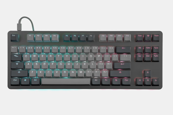 + +The Massdrop CTRL is a TKL mechanical keyboard featuring dual USB-C connectors, an integrated Hi-Speed USB 2.0 hub, and fully customizable RGB backlighting and underlighting. + +Keyboard Maintainer: [Massdrop](https://github.com/massdrop) +Hardware Supported: Massdrop, Inc. CTRL PCBs utilizing Microchip's ATSAMD51J18A MCU and USB2422 2-Port USB 2.0 Hi-Speed Hub Controller, and ISSI's IS31FL3733 LED Drivers. +Hardware Availability: [Massdrop CTRL Mechanical Keyboard](https://www.massdrop.com/buy/massdrop-ctrl-mechanical-keyboard) + +Make example for this keyboard (after setting up your build environment): + + make ctrl:default + +See the [build environment setup](https://docs.qmk.fm/#/getting_started_build_tools) and the [make instructions](https://docs.qmk.fm/#/getting_started_make_guide) for more information. Brand new to QMK? Start with our [Complete Newbs Guide](https://docs.qmk.fm/#/newbs).
\ No newline at end of file diff --git a/keyboards/ctrl/rules.mk b/keyboards/ctrl/rules.mk new file mode 100644 index 000000000..daf679585 --- /dev/null +++ b/keyboards/ctrl/rules.mk @@ -0,0 +1,32 @@ +# project specific files +SRC = led_programs.c +SRC += matrix.c + +#For platform and packs +ARM_ATSAM = SAMD51J18A +MCU = cortex-m4 + +CUSTOM_MATRIX = yes + +# Build Options +# comment out to disable the options. +# +BOOTMAGIC_ENABLE = no # Virtual DIP switch configuration(+1000) +MOUSEKEY_ENABLE = no # Mouse keys(+4700) +EXTRAKEY_ENABLE = yes # Audio control and System control(+450) +CONSOLE_ENABLE = no # Console for debug(+400) +COMMAND_ENABLE = no # Commands for debug and configuration +# Do not enable SLEEP_LED_ENABLE. it uses the same timer as BACKLIGHT_ENABLE +SLEEP_LED_ENABLE = no # Breathing sleep LED during USB suspend +# if this doesn't work, see here: https://github.com/tmk/tmk_keyboard/wiki/FAQ#nkro-doesnt-work +NKRO_ENABLE = yes # USB Nkey Rollover +BACKLIGHT_ENABLE = no # Enable keyboard backlight functionality on B7 by default +RGBLIGHT_ENABLE = no # Enable keyboard RGB underglow +MIDI_ENABLE = no # MIDI support (+2400 to 4200, depending on config) +UNICODE_ENABLE = no # Unicode +BLUETOOTH_ENABLE = no # Enable Bluetooth with the Adafruit EZ-Key HID +AUDIO_ENABLE = no # Audio output on port C6 +FAUXCLICKY_ENABLE = no # Use buzzer to emulate clicky switches +HD44780_ENABLE = no # Enable support for HD44780 based LCDs (+400) +VIRTSER_ENABLE = no # USB Serial Driver +RAW_ENABLE = no # Raw device diff --git a/lib/arm_atsam/packs/arm/cmsis/5.0.1/CMSIS/Include/arm_math.h b/lib/arm_atsam/packs/arm/cmsis/5.0.1/CMSIS/Include/arm_math.h new file mode 100644 index 000000000..4be7e8c84 --- /dev/null +++ b/lib/arm_atsam/packs/arm/cmsis/5.0.1/CMSIS/Include/arm_math.h @@ -0,0 +1,7226 @@ +/* ---------------------------------------------------------------------- + * Project: CMSIS DSP Library + * Title: arm_math.h + * Description: Public header file for CMSIS DSP Library + * + * $Date: 27. January 2017 + * $Revision: V.1.5.1 + * + * Target Processor: Cortex-M cores + * -------------------------------------------------------------------- */ +/* + * Copyright (C) 2010-2017 ARM Limited or its affiliates. All rights reserved. + * + * SPDX-License-Identifier: Apache-2.0 + * + * Licensed under the Apache License, Version 2.0 (the License); you may + * not use this file except in compliance with the License. + * You may obtain a copy of the License at + * + * www.apache.org/licenses/LICENSE-2.0 + * + * Unless required by applicable law or agreed to in writing, software + * distributed under the License is distributed on an AS IS BASIS, WITHOUT + * WARRANTIES OR CONDITIONS OF ANY KIND, either express or implied. + * See the License for the specific language governing permissions and + * limitations under the License. + */ + +/** + \mainpage CMSIS DSP Software Library + * + * Introduction + * ------------ + * + * This user manual describes the CMSIS DSP software library, + * a suite of common signal processing functions for use on Cortex-M processor based devices. + * + * The library is divided into a number of functions each covering a specific category: + * - Basic math functions + * - Fast math functions + * - Complex math functions + * - Filters + * - Matrix functions + * - Transforms + * - Motor control functions + * - Statistical functions + * - Support functions + * - Interpolation functions + * + * The library has separate functions for operating on 8-bit integers, 16-bit integers, + * 32-bit integer and 32-bit floating-point values. + * + * Using the Library + * ------------ + * + * The library installer contains prebuilt versions of the libraries in the <code>Lib</code> folder. + * - arm_cortexM7lfdp_math.lib (Cortex-M7, Little endian, Double Precision Floating Point Unit) + * - arm_cortexM7bfdp_math.lib (Cortex-M7, Big endian, Double Precision Floating Point Unit) + * - arm_cortexM7lfsp_math.lib (Cortex-M7, Little endian, Single Precision Floating Point Unit) + * - arm_cortexM7bfsp_math.lib (Cortex-M7, Big endian and Single Precision Floating Point Unit on) + * - arm_cortexM7l_math.lib (Cortex-M7, Little endian) + * - arm_cortexM7b_math.lib (Cortex-M7, Big endian) + * - arm_cortexM4lf_math.lib (Cortex-M4, Little endian, Floating Point Unit) + * - arm_cortexM4bf_math.lib (Cortex-M4, Big endian, Floating Point Unit) + * - arm_cortexM4l_math.lib (Cortex-M4, Little endian) + * - arm_cortexM4b_math.lib (Cortex-M4, Big endian) + * - arm_cortexM3l_math.lib (Cortex-M3, Little endian) + * - arm_cortexM3b_math.lib (Cortex-M3, Big endian) + * - arm_cortexM0l_math.lib (Cortex-M0 / Cortex-M0+, Little endian) + * - arm_cortexM0b_math.lib (Cortex-M0 / Cortex-M0+, Big endian) + * - arm_ARMv8MBLl_math.lib (ARMv8M Baseline, Little endian) + * - arm_ARMv8MMLl_math.lib (ARMv8M Mainline, Little endian) + * - arm_ARMv8MMLlfsp_math.lib (ARMv8M Mainline, Little endian, Single Precision Floating Point Unit) + * - arm_ARMv8MMLld_math.lib (ARMv8M Mainline, Little endian, DSP instructions) + * - arm_ARMv8MMLldfsp_math.lib (ARMv8M Mainline, Little endian, DSP instructions, Single Precision Floating Point Unit) + * + * The library functions are declared in the public file <code>arm_math.h</code> which is placed in the <code>Include</code> folder. + * Simply include this file and link the appropriate library in the application and begin calling the library functions. The Library supports single + * public header file <code> arm_math.h</code> for Cortex-M cores with little endian and big endian. Same header file will be used for floating point unit(FPU) variants. + * Define the appropriate pre processor MACRO ARM_MATH_CM7 or ARM_MATH_CM4 or ARM_MATH_CM3 or + * ARM_MATH_CM0 or ARM_MATH_CM0PLUS depending on the target processor in the application. + * For ARMv8M cores define pre processor MACRO ARM_MATH_ARMV8MBL or ARM_MATH_ARMV8MML. + * Set Pre processor MACRO __DSP_PRESENT if ARMv8M Mainline core supports DSP instructions. + * + * + * Examples + * -------- + * + * The library ships with a number of examples which demonstrate how to use the library functions. + * + * Toolchain Support + * ------------ + * + * The library has been developed and tested with MDK-ARM version 5.14.0.0 + * The library is being tested in GCC and IAR toolchains and updates on this activity will be made available shortly. + * + * Building the Library + * ------------ + * + * The library installer contains a project file to re build libraries on MDK-ARM Tool chain in the <code>CMSIS\\DSP_Lib\\Source\\ARM</code> folder. + * - arm_cortexM_math.uvprojx + * + * + * The libraries can be built by opening the arm_cortexM_math.uvprojx project in MDK-ARM, selecting a specific target, and defining the optional pre processor MACROs detailed above. + * + * Pre-processor Macros + * ------------ + * + * Each library project have differant pre-processor macros. + * + * - UNALIGNED_SUPPORT_DISABLE: + * + * Define macro UNALIGNED_SUPPORT_DISABLE, If the silicon does not support unaligned memory access + * + * - ARM_MATH_BIG_ENDIAN: + * + * Define macro ARM_MATH_BIG_ENDIAN to build the library for big endian targets. By default library builds for little endian targets. + * + * - ARM_MATH_MATRIX_CHECK: + * + * Define macro ARM_MATH_MATRIX_CHECK for checking on the input and output sizes of matrices + * + * - ARM_MATH_ROUNDING: + * + * Define macro ARM_MATH_ROUNDING for rounding on support functions + * + * - ARM_MATH_CMx: + * + * Define macro ARM_MATH_CM4 for building the library on Cortex-M4 target, ARM_MATH_CM3 for building library on Cortex-M3 target + * and ARM_MATH_CM0 for building library on Cortex-M0 target, ARM_MATH_CM0PLUS for building library on Cortex-M0+ target, and + * ARM_MATH_CM7 for building the library on cortex-M7. + * + * - ARM_MATH_ARMV8MxL: + * + * Define macro ARM_MATH_ARMV8MBL for building the library on ARMv8M Baseline target, ARM_MATH_ARMV8MBL for building library + * on ARMv8M Mainline target. + * + * - __FPU_PRESENT: + * + * Initialize macro __FPU_PRESENT = 1 when building on FPU supported Targets. Enable this macro for floating point libraries. + * + * - __DSP_PRESENT: + * + * Initialize macro __DSP_PRESENT = 1 when ARMv8M Mainline core supports DSP instructions. + * + * <hr> + * CMSIS-DSP in ARM::CMSIS Pack + * ----------------------------- + * + * The following files relevant to CMSIS-DSP are present in the <b>ARM::CMSIS</b> Pack directories: + * |File/Folder |Content | + * |------------------------------|------------------------------------------------------------------------| + * |\b CMSIS\\Documentation\\DSP | This documentation | + * |\b CMSIS\\DSP_Lib | Software license agreement (license.txt) | + * |\b CMSIS\\DSP_Lib\\Examples | Example projects demonstrating the usage of the library functions | + * |\b CMSIS\\DSP_Lib\\Source | Source files for rebuilding the library | + * + * <hr> + * Revision History of CMSIS-DSP + * ------------ + * Please refer to \ref ChangeLog_pg. + * + * Copyright Notice + * ------------ + * + * Copyright (C) 2010-2015 ARM Limited. All rights reserved. + */ + + +/** + * @defgroup groupMath Basic Math Functions + */ + +/** + * @defgroup groupFastMath Fast Math Functions + * This set of functions provides a fast approximation to sine, cosine, and square root. + * As compared to most of the other functions in the CMSIS math library, the fast math functions + * operate on individual values and not arrays. + * There are separate functions for Q15, Q31, and floating-point data. + * + */ + +/** + * @defgroup groupCmplxMath Complex Math Functions + * This set of functions operates on complex data vectors. + * The data in the complex arrays is stored in an interleaved fashion + * (real, imag, real, imag, ...). + * In the API functions, the number of samples in a complex array refers + * to the number of complex values; the array contains twice this number of + * real values. + */ + +/** + * @defgroup groupFilters Filtering Functions + */ + +/** + * @defgroup groupMatrix Matrix Functions + * + * This set of functions provides basic matrix math operations. + * The functions operate on matrix data structures. For example, + * the type + * definition for the floating-point matrix structure is shown + * below: + * <pre> + * typedef struct + * { + * uint16_t numRows; // number of rows of the matrix. + * uint16_t numCols; // number of columns of the matrix. + * float32_t *pData; // points to the data of the matrix. + * } arm_matrix_instance_f32; + * </pre> + * There are similar definitions for Q15 and Q31 data types. + * + * The structure specifies the size of the matrix and then points to + * an array of data. The array is of size <code>numRows X numCols</code> + * and the values are arranged in row order. That is, the + * matrix element (i, j) is stored at: + * <pre> + * pData[i*numCols + j] + * </pre> + * + * \par Init Functions + * There is an associated initialization function for each type of matrix + * data structure. + * The initialization function sets the values of the internal structure fields. + * Refer to the function <code>arm_mat_init_f32()</code>, <code>arm_mat_init_q31()</code> + * and <code>arm_mat_init_q15()</code> for floating-point, Q31 and Q15 types, respectively. + * + * \par + * Use of the initialization function is optional. However, if initialization function is used + * then the instance structure cannot be placed into a const data section. + * To place the instance structure in a const data + * section, manually initialize the data structure. For example: + * <pre> + * <code>arm_matrix_instance_f32 S = {nRows, nColumns, pData};</code> + * <code>arm_matrix_instance_q31 S = {nRows, nColumns, pData};</code> + * <code>arm_matrix_instance_q15 S = {nRows, nColumns, pData};</code> + * </pre> + * where <code>nRows</code> specifies the number of rows, <code>nColumns</code> + * specifies the number of columns, and <code>pData</code> points to the + * data array. + * + * \par Size Checking + * By default all of the matrix functions perform size checking on the input and + * output matrices. For example, the matrix addition function verifies that the + * two input matrices and the output matrix all have the same number of rows and + * columns. If the size check fails the functions return: + * <pre> + * ARM_MATH_SIZE_MISMATCH + * </pre> + * Otherwise the functions return + * <pre> + * ARM_MATH_SUCCESS + * </pre> + * There is some overhead associated with this matrix size checking. + * The matrix size checking is enabled via the \#define + * <pre> + * ARM_MATH_MATRIX_CHECK + * </pre> + * within the library project settings. By default this macro is defined + * and size checking is enabled. By changing the project settings and + * undefining this macro size checking is eliminated and the functions + * run a bit faster. With size checking disabled the functions always + * return <code>ARM_MATH_SUCCESS</code>. + */ + +/** + * @defgroup groupTransforms Transform Functions + */ + +/** + * @defgroup groupController Controller Functions + */ + +/** + * @defgroup groupStats Statistics Functions + */ +/** + * @defgroup groupSupport Support Functions + */ + +/** + * @defgroup groupInterpolation Interpolation Functions + * These functions perform 1- and 2-dimensional interpolation of data. + * Linear interpolation is used for 1-dimensional data and + * bilinear interpolation is used for 2-dimensional data. + */ + +/** + * @defgroup groupExamples Examples + */ +#ifndef _ARM_MATH_H +#define _ARM_MATH_H + +/* ignore some GCC warnings */ +#if defined ( __GNUC__ ) +#pragma GCC diagnostic push +#pragma GCC diagnostic ignored "-Wsign-conversion" +#pragma GCC diagnostic ignored "-Wconversion" +#pragma GCC diagnostic ignored "-Wunused-parameter" +#endif + +#define __CMSIS_GENERIC /* disable NVIC and Systick functions */ + +#if defined(ARM_MATH_CM7) + #include "core_cm7.h" + #define ARM_MATH_DSP +#elif defined (ARM_MATH_CM4) + #include "core_cm4.h" + #define ARM_MATH_DSP +#elif defined (ARM_MATH_CM3) + #include "core_cm3.h" +#elif defined (ARM_MATH_CM0) + #include "core_cm0.h" + #define ARM_MATH_CM0_FAMILY +#elif defined (ARM_MATH_CM0PLUS) + #include "core_cm0plus.h" + #define ARM_MATH_CM0_FAMILY +#elif defined (ARM_MATH_ARMV8MBL) + #include "core_armv8mbl.h" + #define ARM_MATH_CM0_FAMILY +#elif defined (ARM_MATH_ARMV8MML) + #include "core_armv8mml.h" + #if (defined (__DSP_PRESENT) && (__DSP_PRESENT == 1)) + #define ARM_MATH_DSP + #endif +#else + #error "Define according the used Cortex core ARM_MATH_CM7, ARM_MATH_CM4, ARM_MATH_CM3, ARM_MATH_CM0PLUS, ARM_MATH_CM0, ARM_MATH_ARMV8MBL, ARM_MATH_ARMV8MML" +#endif + +#undef __CMSIS_GENERIC /* enable NVIC and Systick functions */ +#include "string.h" +#include "math.h" +#ifdef __cplusplus +extern "C" +{ +#endif + + + /** + * @brief Macros required for reciprocal calculation in Normalized LMS + */ + +#define DELTA_Q31 (0x100) +#define DELTA_Q15 0x5 +#define INDEX_MASK 0x0000003F +#ifndef PI + #define PI 3.14159265358979f +#endif + + /** + * @brief Macros required for SINE and COSINE Fast math approximations + */ + +#define FAST_MATH_TABLE_SIZE 512 +#define FAST_MATH_Q31_SHIFT (32 - 10) +#define FAST_MATH_Q15_SHIFT (16 - 10) +#define CONTROLLER_Q31_SHIFT (32 - 9) +#define TABLE_SPACING_Q31 0x400000 +#define TABLE_SPACING_Q15 0x80 + + /** + * @brief Macros required for SINE and COSINE Controller functions + */ + /* 1.31(q31) Fixed value of 2/360 */ + /* -1 to +1 is divided into 360 values so total spacing is (2/360) */ +#define INPUT_SPACING 0xB60B61 + + /** + * @brief Macro for Unaligned Support + */ +#ifndef UNALIGNED_SUPPORT_DISABLE + #define ALIGN4 +#else + #if defined (__GNUC__) + #define ALIGN4 __attribute__((aligned(4))) + #else + #define ALIGN4 __align(4) + #endif +#endif /* #ifndef UNALIGNED_SUPPORT_DISABLE */ + + /** + * @brief Error status returned by some functions in the library. + */ + + typedef enum + { + ARM_MATH_SUCCESS = 0, /**< No error */ + ARM_MATH_ARGUMENT_ERROR = -1, /**< One or more arguments are incorrect */ + ARM_MATH_LENGTH_ERROR = -2, /**< Length of data buffer is incorrect */ + ARM_MATH_SIZE_MISMATCH = -3, /**< Size of matrices is not compatible with the operation. */ + ARM_MATH_NANINF = -4, /**< Not-a-number (NaN) or infinity is generated */ + ARM_MATH_SINGULAR = -5, /**< Generated by matrix inversion if the input matrix is singular and cannot be inverted. */ + ARM_MATH_TEST_FAILURE = -6 /**< Test Failed */ + } arm_status; + + /** + * @brief 8-bit fractional data type in 1.7 format. + */ + typedef int8_t q7_t; + + /** + * @brief 16-bit fractional data type in 1.15 format. + */ + typedef int16_t q15_t; + + /** + * @brief 32-bit fractional data type in 1.31 format. + */ + typedef int32_t q31_t; + + /** + * @brief 64-bit fractional data type in 1.63 format. + */ + typedef int64_t q63_t; + + /** + * @brief 32-bit floating-point type definition. + */ + typedef float float32_t; + + /** + * @brief 64-bit floating-point type definition. + */ + typedef double float64_t; + + /** + * @brief definition to read/write two 16 bit values. + */ +#if defined ( __CC_ARM ) + #define __SIMD32_TYPE int32_t __packed + #define CMSIS_UNUSED __attribute__((unused)) + #define CMSIS_INLINE __attribute__((always_inline)) + +#elif defined ( __ARMCC_VERSION ) && ( __ARMCC_VERSION >= 6010050 ) + #define __SIMD32_TYPE int32_t + #define CMSIS_UNUSED __attribute__((unused)) + #define CMSIS_INLINE __attribute__((always_inline)) + +#elif defined ( __GNUC__ ) + #define __SIMD32_TYPE int32_t + #define CMSIS_UNUSED __attribute__((unused)) + #define CMSIS_INLINE __attribute__((always_inline)) + +#elif defined ( __ICCARM__ ) + #define __SIMD32_TYPE int32_t __packed + #define CMSIS_UNUSED + #define CMSIS_INLINE + +#elif defined ( __TI_ARM__ ) + #define __SIMD32_TYPE int32_t + #define CMSIS_UNUSED __attribute__((unused)) + #define CMSIS_INLINE + +#elif defined ( __CSMC__ ) + #define __SIMD32_TYPE int32_t + #define CMSIS_UNUSED + #define CMSIS_INLINE + +#elif defined ( __TASKING__ ) + #define __SIMD32_TYPE __unaligned int32_t + #define CMSIS_UNUSED + #define CMSIS_INLINE + +#else + #error Unknown compiler +#endif + +#define __SIMD32(addr) (*(__SIMD32_TYPE **) & (addr)) +#define __SIMD32_CONST(addr) ((__SIMD32_TYPE *)(addr)) +#define _SIMD32_OFFSET(addr) (*(__SIMD32_TYPE *) (addr)) +#define __SIMD64(addr) (*(int64_t **) & (addr)) + +/* #if defined (ARM_MATH_CM3) || defined (ARM_MATH_CM0_FAMILY) */ +#if !defined (ARM_MATH_DSP) + /** + * @brief definition to pack two 16 bit values. + */ +#define __PKHBT(ARG1, ARG2, ARG3) ( (((int32_t)(ARG1) << 0) & (int32_t)0x0000FFFF) | \ + (((int32_t)(ARG2) << ARG3) & (int32_t)0xFFFF0000) ) +#define __PKHTB(ARG1, ARG2, ARG3) ( (((int32_t)(ARG1) << 0) & (int32_t)0xFFFF0000) | \ + (((int32_t)(ARG2) >> ARG3) & (int32_t)0x0000FFFF) ) + +/* #endif // defined (ARM_MATH_CM3) || defined (ARM_MATH_CM0_FAMILY) */ +#endif /* !defined (ARM_MATH_DSP) */ + + /** + * @brief definition to pack four 8 bit values. + */ +#ifndef ARM_MATH_BIG_ENDIAN + +#define __PACKq7(v0,v1,v2,v3) ( (((int32_t)(v0) << 0) & (int32_t)0x000000FF) | \ + (((int32_t)(v1) << 8) & (int32_t)0x0000FF00) | \ + (((int32_t)(v2) << 16) & (int32_t)0x00FF0000) | \ + (((int32_t)(v3) << 24) & (int32_t)0xFF000000) ) +#else + +#define __PACKq7(v0,v1,v2,v3) ( (((int32_t)(v3) << 0) & (int32_t)0x000000FF) | \ + (((int32_t)(v2) << 8) & (int32_t)0x0000FF00) | \ + (((int32_t)(v1) << 16) & (int32_t)0x00FF0000) | \ + (((int32_t)(v0) << 24) & (int32_t)0xFF000000) ) + +#endif + + + /** + * @brief Clips Q63 to Q31 values. + */ + CMSIS_INLINE __STATIC_INLINE q31_t clip_q63_to_q31( + q63_t x) + { + return ((q31_t) (x >> 32) != ((q31_t) x >> 31)) ? + ((0x7FFFFFFF ^ ((q31_t) (x >> 63)))) : (q31_t) x; + } + + /** + * @brief Clips Q63 to Q15 values. + */ + CMSIS_INLINE __STATIC_INLINE q15_t clip_q63_to_q15( + q63_t x) + { + return ((q31_t) (x >> 32) != ((q31_t) x >> 31)) ? + ((0x7FFF ^ ((q15_t) (x >> 63)))) : (q15_t) (x >> 15); + } + + /** + * @brief Clips Q31 to Q7 values. + */ + CMSIS_INLINE __STATIC_INLINE q7_t clip_q31_to_q7( + q31_t x) + { + return ((q31_t) (x >> 24) != ((q31_t) x >> 23)) ? + ((0x7F ^ ((q7_t) (x >> 31)))) : (q7_t) x; + } + + /** + * @brief Clips Q31 to Q15 values. + */ + CMSIS_INLINE __STATIC_INLINE q15_t clip_q31_to_q15( + q31_t x) + { + return ((q31_t) (x >> 16) != ((q31_t) x >> 15)) ? + ((0x7FFF ^ ((q15_t) (x >> 31)))) : (q15_t) x; + } + + /** + * @brief Multiplies 32 X 64 and returns 32 bit result in 2.30 format. + */ + + CMSIS_INLINE __STATIC_INLINE q63_t mult32x64( + q63_t x, + q31_t y) + { + return ((((q63_t) (x & 0x00000000FFFFFFFF) * y) >> 32) + + (((q63_t) (x >> 32) * y))); + } + +/* + #if defined (ARM_MATH_CM0_FAMILY) && defined ( __CC_ARM ) + #define __CLZ __clz + #endif + */ +/* note: function can be removed when all toolchain support __CLZ for Cortex-M0 */ +#if defined (ARM_MATH_CM0_FAMILY) && ((defined (__ICCARM__)) ) + CMSIS_INLINE __STATIC_INLINE uint32_t __CLZ( + q31_t data); + + CMSIS_INLINE __STATIC_INLINE uint32_t __CLZ( + q31_t data) + { + uint32_t count = 0; + uint32_t mask = 0x80000000; + + while ((data & mask) == 0) + { + count += 1u; + mask = mask >> 1u; + } + + return (count); + } +#endif + + /** + * @brief Function to Calculates 1/in (reciprocal) value of Q31 Data type. + */ + + CMSIS_INLINE __STATIC_INLINE uint32_t arm_recip_q31( + q31_t in, + q31_t * dst, + q31_t * pRecipTable) + { + q31_t out; + uint32_t tempVal; + uint32_t index, i; + uint32_t signBits; + + if (in > 0) + { + signBits = ((uint32_t) (__CLZ( in) - 1)); + } + else + { + signBits = ((uint32_t) (__CLZ(-in) - 1)); + } + + /* Convert input sample to 1.31 format */ + in = (in << signBits); + + /* calculation of index for initial approximated Val */ + index = (uint32_t)(in >> 24); + index = (index & INDEX_MASK); + + /* 1.31 with exp 1 */ + out = pRecipTable[index]; + + /* calculation of reciprocal value */ + /* running approximation for two iterations */ + for (i = 0u; i < 2u; i++) + { + tempVal = (uint32_t) (((q63_t) in * out) >> 31); + tempVal = 0x7FFFFFFFu - tempVal; + /* 1.31 with exp 1 */ + /* out = (q31_t) (((q63_t) out * tempVal) >> 30); */ + out = clip_q63_to_q31(((q63_t) out * tempVal) >> 30); + } + + /* write output */ + *dst = out; + + /* return num of signbits of out = 1/in value */ + return (signBits + 1u); + } + + + /** + * @brief Function to Calculates 1/in (reciprocal) value of Q15 Data type. + */ + CMSIS_INLINE __STATIC_INLINE uint32_t arm_recip_q15( + q15_t in, + q15_t * dst, + q15_t * pRecipTable) + { + q15_t out = 0; + uint32_t tempVal = 0; + uint32_t index = 0, i = 0; + uint32_t signBits = 0; + + if (in > 0) + { + signBits = ((uint32_t)(__CLZ( in) - 17)); + } + else + { + signBits = ((uint32_t)(__CLZ(-in) - 17)); + } + + /* Convert input sample to 1.15 format */ + in = (in << signBits); + + /* calculation of index for initial approximated Val */ + index = (uint32_t)(in >> 8); + index = (index & INDEX_MASK); + + /* 1.15 with exp 1 */ + out = pRecipTable[index]; + + /* calculation of reciprocal value */ + /* running approximation for two iterations */ + for (i = 0u; i < 2u; i++) + { + tempVal = (uint32_t) (((q31_t) in * out) >> 15); + tempVal = 0x7FFFu - tempVal; + /* 1.15 with exp 1 */ + out = (q15_t) (((q31_t) out * tempVal) >> 14); + /* out = clip_q31_to_q15(((q31_t) out * tempVal) >> 14); */ + } + + /* write output */ + *dst = out; + + /* return num of signbits of out = 1/in value */ + return (signBits + 1); + } + + + /* + * @brief C custom defined intrinisic function for only M0 processors + */ +#if defined(ARM_MATH_CM0_FAMILY) + CMSIS_INLINE __STATIC_INLINE q31_t __SSAT( + q31_t x, + uint32_t y) + { + int32_t posMax, negMin; + uint32_t i; + + posMax = 1; + for (i = 0; i < (y - 1); i++) + { + posMax = posMax * 2; + } + + if (x > 0) + { + posMax = (posMax - 1); + + if (x > posMax) + { + x = posMax; + } + } + else + { + negMin = -posMax; + + if (x < negMin) + { + x = negMin; + } + } + return (x); + } +#endif /* end of ARM_MATH_CM0_FAMILY */ + + + /* + * @brief C custom defined intrinsic function for M3 and M0 processors + */ +/* #if defined (ARM_MATH_CM3) || defined (ARM_MATH_CM0_FAMILY) */ +#if !defined (ARM_MATH_DSP) + + /* + * @brief C custom defined QADD8 for M3 and M0 processors + */ + CMSIS_INLINE __STATIC_INLINE uint32_t __QADD8( + uint32_t x, + uint32_t y) + { + q31_t r, s, t, u; + + r = __SSAT(((((q31_t)x << 24) >> 24) + (((q31_t)y << 24) >> 24)), 8) & (int32_t)0x000000FF; + s = __SSAT(((((q31_t)x << 16) >> 24) + (((q31_t)y << 16) >> 24)), 8) & (int32_t)0x000000FF; + t = __SSAT(((((q31_t)x << 8) >> 24) + (((q31_t)y << 8) >> 24)), 8) & (int32_t)0x000000FF; + u = __SSAT(((((q31_t)x ) >> 24) + (((q31_t)y ) >> 24)), 8) & (int32_t)0x000000FF; + + return ((uint32_t)((u << 24) | (t << 16) | (s << 8) | (r ))); + } + + + /* + * @brief C custom defined QSUB8 for M3 and M0 processors + */ + CMSIS_INLINE __STATIC_INLINE uint32_t __QSUB8( + uint32_t x, + uint32_t y) + { + q31_t r, s, t, u; + + r = __SSAT(((((q31_t)x << 24) >> 24) - (((q31_t)y << 24) >> 24)), 8) & (int32_t)0x000000FF; + s = __SSAT(((((q31_t)x << 16) >> 24) - (((q31_t)y << 16) >> 24)), 8) & (int32_t)0x000000FF; + t = __SSAT(((((q31_t)x << 8) >> 24) - (((q31_t)y << 8) >> 24)), 8) & (int32_t)0x000000FF; + u = __SSAT(((((q31_t)x ) >> 24) - (((q31_t)y ) >> 24)), 8) & (int32_t)0x000000FF; + + return ((uint32_t)((u << 24) | (t << 16) | (s << 8) | (r ))); + } + + + /* + * @brief C custom defined QADD16 for M3 and M0 processors + */ + CMSIS_INLINE __STATIC_INLINE uint32_t __QADD16( + uint32_t x, + uint32_t y) + { +/* q31_t r, s; without initialisation 'arm_offset_q15 test' fails but 'intrinsic' tests pass! for armCC */ + q31_t r = 0, s = 0; + + r = __SSAT(((((q31_t)x << 16) >> 16) + (((q31_t)y << 16) >> 16)), 16) & (int32_t)0x0000FFFF; + s = __SSAT(((((q31_t)x ) >> 16) + (((q31_t)y ) >> 16)), 16) & (int32_t)0x0000FFFF; + + return ((uint32_t)((s << 16) | (r ))); + } + + + /* + * @brief C custom defined SHADD16 for M3 and M0 processors + */ + CMSIS_INLINE __STATIC_INLINE uint32_t __SHADD16( + uint32_t x, + uint32_t y) + { + q31_t r, s; + + r = (((((q31_t)x << 16) >> 16) + (((q31_t)y << 16) >> 16)) >> 1) & (int32_t)0x0000FFFF; + s = (((((q31_t)x ) >> 16) + (((q31_t)y ) >> 16)) >> 1) & (int32_t)0x0000FFFF; + + return ((uint32_t)((s << 16) | (r ))); + } + + + /* + * @brief C custom defined QSUB16 for M3 and M0 processors + */ + CMSIS_INLINE __STATIC_INLINE uint32_t __QSUB16( + uint32_t x, + uint32_t y) + { + q31_t r, s; + + r = __SSAT(((((q31_t)x << 16) >> 16) - (((q31_t)y << 16) >> 16)), 16) & (int32_t)0x0000FFFF; + s = __SSAT(((((q31_t)x ) >> 16) - (((q31_t)y ) >> 16)), 16) & (int32_t)0x0000FFFF; + + return ((uint32_t)((s << 16) | (r ))); + } + + + /* + * @brief C custom defined SHSUB16 for M3 and M0 processors + */ + CMSIS_INLINE __STATIC_INLINE uint32_t __SHSUB16( + uint32_t x, + uint32_t y) + { + q31_t r, s; + + r = (((((q31_t)x << 16) >> 16) - (((q31_t)y << 16) >> 16)) >> 1) & (int32_t)0x0000FFFF; + s = (((((q31_t)x ) >> 16) - (((q31_t)y ) >> 16)) >> 1) & (int32_t)0x0000FFFF; + + return ((uint32_t)((s << 16) | (r ))); + } + + + /* + * @brief C custom defined QASX for M3 and M0 processors + */ + CMSIS_INLINE __STATIC_INLINE uint32_t __QASX( + uint32_t x, + uint32_t y) + { + q31_t r, s; + + r = __SSAT(((((q31_t)x << 16) >> 16) - (((q31_t)y ) >> 16)), 16) & (int32_t)0x0000FFFF; + s = __SSAT(((((q31_t)x ) >> 16) + (((q31_t)y << 16) >> 16)), 16) & (int32_t)0x0000FFFF; + + return ((uint32_t)((s << 16) | (r ))); + } + + + /* + * @brief C custom defined SHASX for M3 and M0 processors + */ + CMSIS_INLINE __STATIC_INLINE uint32_t __SHASX( + uint32_t x, + uint32_t y) + { + q31_t r, s; + + r = (((((q31_t)x << 16) >> 16) - (((q31_t)y ) >> 16)) >> 1) & (int32_t)0x0000FFFF; + s = (((((q31_t)x ) >> 16) + (((q31_t)y << 16) >> 16)) >> 1) & (int32_t)0x0000FFFF; + + return ((uint32_t)((s << 16) | (r ))); + } + + + /* + * @brief C custom defined QSAX for M3 and M0 processors + */ + CMSIS_INLINE __STATIC_INLINE uint32_t __QSAX( + uint32_t x, + uint32_t y) + { + q31_t r, s; + + r = __SSAT(((((q31_t)x << 16) >> 16) + (((q31_t)y ) >> 16)), 16) & (int32_t)0x0000FFFF; + s = __SSAT(((((q31_t)x ) >> 16) - (((q31_t)y << 16) >> 16)), 16) & (int32_t)0x0000FFFF; + + return ((uint32_t)((s << 16) | (r ))); + } + + + /* + * @brief C custom defined SHSAX for M3 and M0 processors + */ + CMSIS_INLINE __STATIC_INLINE uint32_t __SHSAX( + uint32_t x, + uint32_t y) + { + q31_t r, s; + + r = (((((q31_t)x << 16) >> 16) + (((q31_t)y ) >> 16)) >> 1) & (int32_t)0x0000FFFF; + s = (((((q31_t)x ) >> 16) - (((q31_t)y << 16) >> 16)) >> 1) & (int32_t)0x0000FFFF; + + return ((uint32_t)((s << 16) | (r ))); + } + + + /* + * @brief C custom defined SMUSDX for M3 and M0 processors + */ + CMSIS_INLINE __STATIC_INLINE uint32_t __SMUSDX( + uint32_t x, + uint32_t y) + { + return ((uint32_t)(((((q31_t)x << 16) >> 16) * (((q31_t)y ) >> 16)) - + ((((q31_t)x ) >> 16) * (((q31_t)y << 16) >> 16)) )); + } + + /* + * @brief C custom defined SMUADX for M3 and M0 processors + */ + CMSIS_INLINE __STATIC_INLINE uint32_t __SMUADX( + uint32_t x, + uint32_t y) + { + return ((uint32_t)(((((q31_t)x << 16) >> 16) * (((q31_t)y ) >> 16)) + + ((((q31_t)x ) >> 16) * (((q31_t)y << 16) >> 16)) )); + } + + + /* + * @brief C custom defined QADD for M3 and M0 processors + */ + CMSIS_INLINE __STATIC_INLINE int32_t __QADD( + int32_t x, + int32_t y) + { + return ((int32_t)(clip_q63_to_q31((q63_t)x + (q31_t)y))); + } + + + /* + * @brief C custom defined QSUB for M3 and M0 processors + */ + CMSIS_INLINE __STATIC_INLINE int32_t __QSUB( + int32_t x, + int32_t y) + { + return ((int32_t)(clip_q63_to_q31((q63_t)x - (q31_t)y))); + } + + + /* + * @brief C custom defined SMLAD for M3 and M0 processors + */ + CMSIS_INLINE __STATIC_INLINE uint32_t __SMLAD( + uint32_t x, + uint32_t y, + uint32_t sum) + { + return ((uint32_t)(((((q31_t)x << 16) >> 16) * (((q31_t)y << 16) >> 16)) + + ((((q31_t)x ) >> 16) * (((q31_t)y ) >> 16)) + + ( ((q31_t)sum ) ) )); + } + + + /* + * @brief C custom defined SMLADX for M3 and M0 processors + */ + CMSIS_INLINE __STATIC_INLINE uint32_t __SMLADX( + uint32_t x, + uint32_t y, + uint32_t sum) + { + return ((uint32_t)(((((q31_t)x << 16) >> 16) * (((q31_t)y ) >> 16)) + + ((((q31_t)x ) >> 16) * (((q31_t)y << 16) >> 16)) + + ( ((q31_t)sum ) ) )); + } + + + /* + * @brief C custom defined SMLSDX for M3 and M0 processors + */ + CMSIS_INLINE __STATIC_INLINE uint32_t __SMLSDX( + uint32_t x, + uint32_t y, + uint32_t sum) + { + return ((uint32_t)(((((q31_t)x << 16) >> 16) * (((q31_t)y ) >> 16)) - + ((((q31_t)x ) >> 16) * (((q31_t)y << 16) >> 16)) + + ( ((q31_t)sum ) ) )); + } + + + /* + * @brief C custom defined SMLALD for M3 and M0 processors + */ + CMSIS_INLINE __STATIC_INLINE uint64_t __SMLALD( + uint32_t x, + uint32_t y, + uint64_t sum) + { +/* return (sum + ((q15_t) (x >> 16) * (q15_t) (y >> 16)) + ((q15_t) x * (q15_t) y)); */ + return ((uint64_t)(((((q31_t)x << 16) >> 16) * (((q31_t)y << 16) >> 16)) + + ((((q31_t)x ) >> 16) * (((q31_t)y ) >> 16)) + + ( ((q63_t)sum ) ) )); + } + + + /* + * @brief C custom defined SMLALDX for M3 and M0 processors + */ + CMSIS_INLINE __STATIC_INLINE uint64_t __SMLALDX( + uint32_t x, + uint32_t y, + uint64_t sum) + { +/* return (sum + ((q15_t) (x >> 16) * (q15_t) y)) + ((q15_t) x * (q15_t) (y >> 16)); */ + return ((uint64_t)(((((q31_t)x << 16) >> 16) * (((q31_t)y ) >> 16)) + + ((((q31_t)x ) >> 16) * (((q31_t)y << 16) >> 16)) + + ( ((q63_t)sum ) ) )); + } + + + /* + * @brief C custom defined SMUAD for M3 and M0 processors + */ + CMSIS_INLINE __STATIC_INLINE uint32_t __SMUAD( + uint32_t x, + uint32_t y) + { + return ((uint32_t)(((((q31_t)x << 16) >> 16) * (((q31_t)y << 16) >> 16)) + + ((((q31_t)x ) >> 16) * (((q31_t)y ) >> 16)) )); + } + + + /* + * @brief C custom defined SMUSD for M3 and M0 processors + */ + CMSIS_INLINE __STATIC_INLINE uint32_t __SMUSD( + uint32_t x, + uint32_t y) + { + return ((uint32_t)(((((q31_t)x << 16) >> 16) * (((q31_t)y << 16) >> 16)) - + ((((q31_t)x ) >> 16) * (((q31_t)y ) >> 16)) )); + } + + + /* + * @brief C custom defined SXTB16 for M3 and M0 processors + */ + CMSIS_INLINE __STATIC_INLINE uint32_t __SXTB16( + uint32_t x) + { + return ((uint32_t)(((((q31_t)x << 24) >> 24) & (q31_t)0x0000FFFF) | + ((((q31_t)x << 8) >> 8) & (q31_t)0xFFFF0000) )); + } + + /* + * @brief C custom defined SMMLA for M3 and M0 processors + */ + CMSIS_INLINE __STATIC_INLINE int32_t __SMMLA( + int32_t x, + int32_t y, + int32_t sum) + { + return (sum + (int32_t) (((int64_t) x * y) >> 32)); + } + +#if 0 + /* + * @brief C custom defined PKHBT for unavailable DSP extension + */ + CMSIS_INLINE __STATIC_INLINE uint32_t __PKHBT( + uint32_t x, + uint32_t y, + uint32_t leftshift) + { + return ( ((x ) & 0x0000FFFFUL) | + ((y << leftshift) & 0xFFFF0000UL) ); + } + + /* + * @brief C custom defined PKHTB for unavailable DSP extension + */ + CMSIS_INLINE __STATIC_INLINE uint32_t __PKHTB( + uint32_t x, + uint32_t y, + uint32_t rightshift) + { + return ( ((x ) & 0xFFFF0000UL) | + ((y >> rightshift) & 0x0000FFFFUL) ); + } +#endif + +/* #endif // defined (ARM_MATH_CM3) || defined (ARM_MATH_CM0_FAMILY) */ +#endif /* !defined (ARM_MATH_DSP) */ + + + /** + * @brief Instance structure for the Q7 FIR filter. + */ + typedef struct + { + uint16_t numTaps; /**< number of filter coefficients in the filter. */ + q7_t *pState; /**< points to the state variable array. The array is of length numTaps+blockSize-1. */ + q7_t *pCoeffs; /**< points to the coefficient array. The array is of length numTaps.*/ + } arm_fir_instance_q7; + + /** + * @brief Instance structure for the Q15 FIR filter. + */ + typedef struct + { + uint16_t numTaps; /**< number of filter coefficients in the filter. */ + q15_t *pState; /**< points to the state variable array. The array is of length numTaps+blockSize-1. */ + q15_t *pCoeffs; /**< points to the coefficient array. The array is of length numTaps.*/ + } arm_fir_instance_q15; + + /** + * @brief Instance structure for the Q31 FIR filter. + */ + typedef struct + { + uint16_t numTaps; /**< number of filter coefficients in the filter. */ + q31_t *pState; /**< points to the state variable array. The array is of length numTaps+blockSize-1. */ + q31_t *pCoeffs; /**< points to the coefficient array. The array is of length numTaps. */ + } arm_fir_instance_q31; + + /** + * @brief Instance structure for the floating-point FIR filter. + */ + typedef struct + { + uint16_t numTaps; /**< number of filter coefficients in the filter. */ + float32_t *pState; /**< points to the state variable array. The array is of length numTaps+blockSize-1. */ + float32_t *pCoeffs; /**< points to the coefficient array. The array is of length numTaps. */ + } arm_fir_instance_f32; + + + /** + * @brief Processing function for the Q7 FIR filter. + * @param[in] S points to an instance of the Q7 FIR filter structure. + * @param[in] pSrc points to the block of input data. + * @param[out] pDst points to the block of output data. + * @param[in] blockSize number of samples to process. + */ + void arm_fir_q7( + const arm_fir_instance_q7 * S, + q7_t * pSrc, + q7_t * pDst, + uint32_t blockSize); + + + /** + * @brief Initialization function for the Q7 FIR filter. + * @param[in,out] S points to an instance of the Q7 FIR structure. + * @param[in] numTaps Number of filter coefficients in the filter. + * @param[in] pCoeffs points to the filter coefficients. + * @param[in] pState points to the state buffer. + * @param[in] blockSize number of samples that are processed. + */ + void arm_fir_init_q7( + arm_fir_instance_q7 * S, + uint16_t numTaps, + q7_t * pCoeffs, + q7_t * pState, + uint32_t blockSize); + + + /** + * @brief Processing function for the Q15 FIR filter. + * @param[in] S points to an instance of the Q15 FIR structure. + * @param[in] pSrc points to the block of input data. + * @param[out] pDst points to the block of output data. + * @param[in] blockSize number of samples to process. + */ + void arm_fir_q15( + const arm_fir_instance_q15 * S, + q15_t * pSrc, + q15_t * pDst, + uint32_t blockSize); + + + /** + * @brief Processing function for the fast Q15 FIR filter for Cortex-M3 and Cortex-M4. + * @param[in] S points to an instance of the Q15 FIR filter structure. + * @param[in] pSrc points to the block of input data. + * @param[out] pDst points to the block of output data. + * @param[in] blockSize number of samples to process. + */ + void arm_fir_fast_q15( + const arm_fir_instance_q15 * S, + q15_t * pSrc, + q15_t * pDst, + uint32_t blockSize); + + + /** + * @brief Initialization function for the Q15 FIR filter. + * @param[in,out] S points to an instance of the Q15 FIR filter structure. + * @param[in] numTaps Number of filter coefficients in the filter. Must be even and greater than or equal to 4. + * @param[in] pCoeffs points to the filter coefficients. + * @param[in] pState points to the state buffer. + * @param[in] blockSize number of samples that are processed at a time. + * @return The function returns ARM_MATH_SUCCESS if initialization was successful or ARM_MATH_ARGUMENT_ERROR if + * <code>numTaps</code> is not a supported value. + */ + arm_status arm_fir_init_q15( + arm_fir_instance_q15 * S, + uint16_t numTaps, + q15_t * pCoeffs, + q15_t * pState, + uint32_t blockSize); + + + /** + * @brief Processing function for the Q31 FIR filter. + * @param[in] S points to an instance of the Q31 FIR filter structure. + * @param[in] pSrc points to the block of input data. + * @param[out] pDst points to the block of output data. + * @param[in] blockSize number of samples to process. + */ + void arm_fir_q31( + const arm_fir_instance_q31 * S, + q31_t * pSrc, + q31_t * pDst, + uint32_t blockSize); + + + /** + * @brief Processing function for the fast Q31 FIR filter for Cortex-M3 and Cortex-M4. + * @param[in] S points to an instance of the Q31 FIR structure. + * @param[in] pSrc points to the block of input data. + * @param[out] pDst points to the block of output data. + * @param[in] blockSize number of samples to process. + */ + void arm_fir_fast_q31( + const arm_fir_instance_q31 * S, + q31_t * pSrc, + q31_t * pDst, + uint32_t blockSize); + + + /** + * @brief Initialization function for the Q31 FIR filter. + * @param[in,out] S points to an instance of the Q31 FIR structure. + * @param[in] numTaps Number of filter coefficients in the filter. + * @param[in] pCoeffs points to the filter coefficients. + * @param[in] pState points to the state buffer. + * @param[in] blockSize number of samples that are processed at a time. + */ + void arm_fir_init_q31( + arm_fir_instance_q31 * S, + uint16_t numTaps, + q31_t * pCoeffs, + q31_t * pState, + uint32_t blockSize); + + + /** + * @brief Processing function for the floating-point FIR filter. + * @param[in] S points to an instance of the floating-point FIR structure. + * @param[in] pSrc points to the block of input data. + * @param[out] pDst points to the block of output data. + * @param[in] blockSize number of samples to process. + */ + void arm_fir_f32( + const arm_fir_instance_f32 * S, + float32_t * pSrc, + float32_t * pDst, + uint32_t blockSize); + + + /** + * @brief Initialization function for the floating-point FIR filter. + * @param[in,out] S points to an instance of the floating-point FIR filter structure. + * @param[in] numTaps Number of filter coefficients in the filter. + * @param[in] pCoeffs points to the filter coefficients. + * @param[in] pState points to the state buffer. + * @param[in] blockSize number of samples that are processed at a time. + */ + void arm_fir_init_f32( + arm_fir_instance_f32 * S, + uint16_t numTaps, + float32_t * pCoeffs, + float32_t * pState, + uint32_t blockSize); + + + /** + * @brief Instance structure for the Q15 Biquad cascade filter. + */ + typedef struct + { + int8_t numStages; /**< number of 2nd order stages in the filter. Overall order is 2*numStages. */ + q15_t *pState; /**< Points to the array of state coefficients. The array is of length 4*numStages. */ + q15_t *pCoeffs; /**< Points to the array of coefficients. The array is of length 5*numStages. */ + int8_t postShift; /**< Additional shift, in bits, applied to each output sample. */ + } arm_biquad_casd_df1_inst_q15; + + /** + * @brief Instance structure for the Q31 Biquad cascade filter. + */ + typedef struct + { + uint32_t numStages; /**< number of 2nd order stages in the filter. Overall order is 2*numStages. */ + q31_t *pState; /**< Points to the array of state coefficients. The array is of length 4*numStages. */ + q31_t *pCoeffs; /**< Points to the array of coefficients. The array is of length 5*numStages. */ + uint8_t postShift; /**< Additional shift, in bits, applied to each output sample. */ + } arm_biquad_casd_df1_inst_q31; + + /** + * @brief Instance structure for the floating-point Biquad cascade filter. + */ + typedef struct + { + uint32_t numStages; /**< number of 2nd order stages in the filter. Overall order is 2*numStages. */ + float32_t *pState; /**< Points to the array of state coefficients. The array is of length 4*numStages. */ + float32_t *pCoeffs; /**< Points to the array of coefficients. The array is of length 5*numStages. */ + } arm_biquad_casd_df1_inst_f32; + + + /** + * @brief Processing function for the Q15 Biquad cascade filter. + * @param[in] S points to an instance of the Q15 Biquad cascade structure. + * @param[in] pSrc points to the block of input data. + * @param[out] pDst points to the block of output data. + * @param[in] blockSize number of samples to process. + */ + void arm_biquad_cascade_df1_q15( + const arm_biquad_casd_df1_inst_q15 * S, + q15_t * pSrc, + q15_t * pDst, + uint32_t blockSize); + + + /** + * @brief Initialization function for the Q15 Biquad cascade filter. + * @param[in,out] S points to an instance of the Q15 Biquad cascade structure. + * @param[in] numStages number of 2nd order stages in the filter. + * @param[in] pCoeffs points to the filter coefficients. + * @param[in] pState points to the state buffer. + * @param[in] postShift Shift to be applied to the output. Varies according to the coefficients format + */ + void arm_biquad_cascade_df1_init_q15( + arm_biquad_casd_df1_inst_q15 * S, + uint8_t numStages, + q15_t * pCoeffs, + q15_t * pState, + int8_t postShift); + + + /** + * @brief Fast but less precise processing function for the Q15 Biquad cascade filter for Cortex-M3 and Cortex-M4. + * @param[in] S points to an instance of the Q15 Biquad cascade structure. + * @param[in] pSrc points to the block of input data. + * @param[out] pDst points to the block of output data. + * @param[in] blockSize number of samples to process. + */ + void arm_biquad_cascade_df1_fast_q15( + const arm_biquad_casd_df1_inst_q15 * S, + q15_t * pSrc, + q15_t * pDst, + uint32_t blockSize); + + + /** + * @brief Processing function for the Q31 Biquad cascade filter + * @param[in] S points to an instance of the Q31 Biquad cascade structure. + * @param[in] pSrc points to the block of input data. + * @param[out] pDst points to the block of output data. + * @param[in] blockSize number of samples to process. + */ + void arm_biquad_cascade_df1_q31( + const arm_biquad_casd_df1_inst_q31 * S, + q31_t * pSrc, + q31_t * pDst, + uint32_t blockSize); + + + /** + * @brief Fast but less precise processing function for the Q31 Biquad cascade filter for Cortex-M3 and Cortex-M4. + * @param[in] S points to an instance of the Q31 Biquad cascade structure. + * @param[in] pSrc points to the block of input data. + * @param[out] pDst points to the block of output data. + * @param[in] blockSize number of samples to process. + */ + void arm_biquad_cascade_df1_fast_q31( + const arm_biquad_casd_df1_inst_q31 * S, + q31_t * pSrc, + q31_t * pDst, + uint32_t blockSize); + + + /** + * @brief Initialization function for the Q31 Biquad cascade filter. + * @param[in,out] S points to an instance of the Q31 Biquad cascade structure. + * @param[in] numStages number of 2nd order stages in the filter. + * @param[in] pCoeffs points to the filter coefficients. + * @param[in] pState points to the state buffer. + * @param[in] postShift Shift to be applied to the output. Varies according to the coefficients format + */ + void arm_biquad_cascade_df1_init_q31( + arm_biquad_casd_df1_inst_q31 * S, + uint8_t numStages, + q31_t * pCoeffs, + q31_t * pState, + int8_t postShift); + + + /** + * @brief Processing function for the floating-point Biquad cascade filter. + * @param[in] S points to an instance of the floating-point Biquad cascade structure. + * @param[in] pSrc points to the block of input data. + * @param[out] pDst points to the block of output data. + * @param[in] blockSize number of samples to process. + */ + void arm_biquad_cascade_df1_f32( + const arm_biquad_casd_df1_inst_f32 * S, + float32_t * pSrc, + float32_t * pDst, + uint32_t blockSize); + + + /** + * @brief Initialization function for the floating-point Biquad cascade filter. + * @param[in,out] S points to an instance of the floating-point Biquad cascade structure. + * @param[in] numStages number of 2nd order stages in the filter. + * @param[in] pCoeffs points to the filter coefficients. + * @param[in] pState points to the state buffer. + */ + void arm_biquad_cascade_df1_init_f32( + arm_biquad_casd_df1_inst_f32 * S, + uint8_t numStages, + float32_t * pCoeffs, + float32_t * pState); + + + /** + * @brief Instance structure for the floating-point matrix structure. + */ + typedef struct + { + uint16_t numRows; /**< number of rows of the matrix. */ + uint16_t numCols; /**< number of columns of the matrix. */ + float32_t *pData; /**< points to the data of the matrix. */ + } arm_matrix_instance_f32; + + + /** + * @brief Instance structure for the floating-point matrix structure. + */ + typedef struct + { + uint16_t numRows; /**< number of rows of the matrix. */ + uint16_t numCols; /**< number of columns of the matrix. */ + float64_t *pData; /**< points to the data of the matrix. */ + } arm_matrix_instance_f64; + + /** + * @brief Instance structure for the Q15 matrix structure. + */ + typedef struct + { + uint16_t numRows; /**< number of rows of the matrix. */ + uint16_t numCols; /**< number of columns of the matrix. */ + q15_t *pData; /**< points to the data of the matrix. */ + } arm_matrix_instance_q15; + + /** + * @brief Instance structure for the Q31 matrix structure. + */ + typedef struct + { + uint16_t numRows; /**< number of rows of the matrix. */ + uint16_t numCols; /**< number of columns of the matrix. */ + q31_t *pData; /**< points to the data of the matrix. */ + } arm_matrix_instance_q31; + + + /** + * @brief Floating-point matrix addition. + * @param[in] pSrcA points to the first input matrix structure + * @param[in] pSrcB points to the second input matrix structure + * @param[out] pDst points to output matrix structure + * @return The function returns either + * <code>ARM_MATH_SIZE_MISMATCH</code> or <code>ARM_MATH_SUCCESS</code> based on the outcome of size checking. + */ + arm_status arm_mat_add_f32( + const arm_matrix_instance_f32 * pSrcA, + const arm_matrix_instance_f32 * pSrcB, + arm_matrix_instance_f32 * pDst); + + + /** + * @brief Q15 matrix addition. + * @param[in] pSrcA points to the first input matrix structure + * @param[in] pSrcB points to the second input matrix structure + * @param[out] pDst points to output matrix structure + * @return The function returns either + * <code>ARM_MATH_SIZE_MISMATCH</code> or <code>ARM_MATH_SUCCESS</code> based on the outcome of size checking. + */ + arm_status arm_mat_add_q15( + const arm_matrix_instance_q15 * pSrcA, + const arm_matrix_instance_q15 * pSrcB, + arm_matrix_instance_q15 * pDst); + + + /** + * @brief Q31 matrix addition. + * @param[in] pSrcA points to the first input matrix structure + * @param[in] pSrcB points to the second input matrix structure + * @param[out] pDst points to output matrix structure + * @return The function returns either + * <code>ARM_MATH_SIZE_MISMATCH</code> or <code>ARM_MATH_SUCCESS</code> based on the outcome of size checking. + */ + arm_status arm_mat_add_q31( + const arm_matrix_instance_q31 * pSrcA, + const arm_matrix_instance_q31 * pSrcB, + arm_matrix_instance_q31 * pDst); + + + /** + * @brief Floating-point, complex, matrix multiplication. + * @param[in] pSrcA points to the first input matrix structure + * @param[in] pSrcB points to the second input matrix structure + * @param[out] pDst points to output matrix structure + * @return The function returns either + * <code>ARM_MATH_SIZE_MISMATCH</code> or <code>ARM_MATH_SUCCESS</code> based on the outcome of size checking. + */ + arm_status arm_mat_cmplx_mult_f32( + const arm_matrix_instance_f32 * pSrcA, + const arm_matrix_instance_f32 * pSrcB, + arm_matrix_instance_f32 * pDst); + + + /** + * @brief Q15, complex, matrix multiplication. + * @param[in] pSrcA points to the first input matrix structure + * @param[in] pSrcB points to the second input matrix structure + * @param[out] pDst points to output matrix structure + * @return The function returns either + * <code>ARM_MATH_SIZE_MISMATCH</code> or <code>ARM_MATH_SUCCESS</code> based on the outcome of size checking. + */ + arm_status arm_mat_cmplx_mult_q15( + const arm_matrix_instance_q15 * pSrcA, + const arm_matrix_instance_q15 * pSrcB, + arm_matrix_instance_q15 * pDst, + q15_t * pScratch); + + + /** + * @brief Q31, complex, matrix multiplication. + * @param[in] pSrcA points to the first input matrix structure + * @param[in] pSrcB points to the second input matrix structure + * @param[out] pDst points to output matrix structure + * @return The function returns either + * <code>ARM_MATH_SIZE_MISMATCH</code> or <code>ARM_MATH_SUCCESS</code> based on the outcome of size checking. + */ + arm_status arm_mat_cmplx_mult_q31( + const arm_matrix_instance_q31 * pSrcA, + const arm_matrix_instance_q31 * pSrcB, + arm_matrix_instance_q31 * pDst); + + + /** + * @brief Floating-point matrix transpose. + * @param[in] pSrc points to the input matrix + * @param[out] pDst points to the output matrix + * @return The function returns either <code>ARM_MATH_SIZE_MISMATCH</code> + * or <code>ARM_MATH_SUCCESS</code> based on the outcome of size checking. + */ + arm_status arm_mat_trans_f32( + const arm_matrix_instance_f32 * pSrc, + arm_matrix_instance_f32 * pDst); + + + /** + * @brief Q15 matrix transpose. + * @param[in] pSrc points to the input matrix + * @param[out] pDst points to the output matrix + * @return The function returns either <code>ARM_MATH_SIZE_MISMATCH</code> + * or <code>ARM_MATH_SUCCESS</code> based on the outcome of size checking. + */ + arm_status arm_mat_trans_q15( + const arm_matrix_instance_q15 * pSrc, + arm_matrix_instance_q15 * pDst); + + + /** + * @brief Q31 matrix transpose. + * @param[in] pSrc points to the input matrix + * @param[out] pDst points to the output matrix + * @return The function returns either <code>ARM_MATH_SIZE_MISMATCH</code> + * or <code>ARM_MATH_SUCCESS</code> based on the outcome of size checking. + */ + arm_status arm_mat_trans_q31( + const arm_matrix_instance_q31 * pSrc, + arm_matrix_instance_q31 * pDst); + + + /** + * @brief Floating-point matrix multiplication + * @param[in] pSrcA points to the first input matrix structure + * @param[in] pSrcB points to the second input matrix structure + * @param[out] pDst points to output matrix structure + * @return The function returns either + * <code>ARM_MATH_SIZE_MISMATCH</code> or <code>ARM_MATH_SUCCESS</code> based on the outcome of size checking. + */ + arm_status arm_mat_mult_f32( + const arm_matrix_instance_f32 * pSrcA, + const arm_matrix_instance_f32 * pSrcB, + arm_matrix_instance_f32 * pDst); + + + /** + * @brief Q15 matrix multiplication + * @param[in] pSrcA points to the first input matrix structure + * @param[in] pSrcB points to the second input matrix structure + * @param[out] pDst points to output matrix structure + * @param[in] pState points to the array for storing intermediate results + * @return The function returns either + * <code>ARM_MATH_SIZE_MISMATCH</code> or <code>ARM_MATH_SUCCESS</code> based on the outcome of size checking. + */ + arm_status arm_mat_mult_q15( + const arm_matrix_instance_q15 * pSrcA, + const arm_matrix_instance_q15 * pSrcB, + arm_matrix_instance_q15 * pDst, + q15_t * pState); + + + /** + * @brief Q15 matrix multiplication (fast variant) for Cortex-M3 and Cortex-M4 + * @param[in] pSrcA points to the first input matrix structure + * @param[in] pSrcB points to the second input matrix structure + * @param[out] pDst points to output matrix structure + * @param[in] pState points to the array for storing intermediate results + * @return The function returns either + * <code>ARM_MATH_SIZE_MISMATCH</code> or <code>ARM_MATH_SUCCESS</code> based on the outcome of size checking. + */ + arm_status arm_mat_mult_fast_q15( + const arm_matrix_instance_q15 * pSrcA, + const arm_matrix_instance_q15 * pSrcB, + arm_matrix_instance_q15 * pDst, + q15_t * pState); + + + /** + * @brief Q31 matrix multiplication + * @param[in] pSrcA points to the first input matrix structure + * @param[in] pSrcB points to the second input matrix structure + * @param[out] pDst points to output matrix structure + * @return The function returns either + * <code>ARM_MATH_SIZE_MISMATCH</code> or <code>ARM_MATH_SUCCESS</code> based on the outcome of size checking. + */ + arm_status arm_mat_mult_q31( + const arm_matrix_instance_q31 * pSrcA, + const arm_matrix_instance_q31 * pSrcB, + arm_matrix_instance_q31 * pDst); + + + /** + * @brief Q31 matrix multiplication (fast variant) for Cortex-M3 and Cortex-M4 + * @param[in] pSrcA points to the first input matrix structure + * @param[in] pSrcB points to the second input matrix structure + * @param[out] pDst points to output matrix structure + * @return The function returns either + * <code>ARM_MATH_SIZE_MISMATCH</code> or <code>ARM_MATH_SUCCESS</code> based on the outcome of size checking. + */ + arm_status arm_mat_mult_fast_q31( + const arm_matrix_instance_q31 * pSrcA, + const arm_matrix_instance_q31 * pSrcB, + arm_matrix_instance_q31 * pDst); + + + /** + * @brief Floating-point matrix subtraction + * @param[in] pSrcA points to the first input matrix structure + * @param[in] pSrcB points to the second input matrix structure + * @param[out] pDst points to output matrix structure + * @return The function returns either + * <code>ARM_MATH_SIZE_MISMATCH</code> or <code>ARM_MATH_SUCCESS</code> based on the outcome of size checking. + */ + arm_status arm_mat_sub_f32( + const arm_matrix_instance_f32 * pSrcA, + const arm_matrix_instance_f32 * pSrcB, + arm_matrix_instance_f32 * pDst); + + + /** + * @brief Q15 matrix subtraction + * @param[in] pSrcA points to the first input matrix structure + * @param[in] pSrcB points to the second input matrix structure + * @param[out] pDst points to output matrix structure + * @return The function returns either + * <code>ARM_MATH_SIZE_MISMATCH</code> or <code>ARM_MATH_SUCCESS</code> based on the outcome of size checking. + */ + arm_status arm_mat_sub_q15( + const arm_matrix_instance_q15 * pSrcA, + const arm_matrix_instance_q15 * pSrcB, + arm_matrix_instance_q15 * pDst); + + + /** + * @brief Q31 matrix subtraction + * @param[in] pSrcA points to the first input matrix structure + * @param[in] pSrcB points to the second input matrix structure + * @param[out] pDst points to output matrix structure + * @return The function returns either + * <code>ARM_MATH_SIZE_MISMATCH</code> or <code>ARM_MATH_SUCCESS</code> based on the outcome of size checking. + */ + arm_status arm_mat_sub_q31( + const arm_matrix_instance_q31 * pSrcA, + const arm_matrix_instance_q31 * pSrcB, + arm_matrix_instance_q31 * pDst); + + + /** + * @brief Floating-point matrix scaling. + * @param[in] pSrc points to the input matrix + * @param[in] scale scale factor + * @param[out] pDst points to the output matrix + * @return The function returns either + * <code>ARM_MATH_SIZE_MISMATCH</code> or <code>ARM_MATH_SUCCESS</code> based on the outcome of size checking. + */ + arm_status arm_mat_scale_f32( + const arm_matrix_instance_f32 * pSrc, + float32_t scale, + arm_matrix_instance_f32 * pDst); + + + /** + * @brief Q15 matrix scaling. + * @param[in] pSrc points to input matrix + * @param[in] scaleFract fractional portion of the scale factor + * @param[in] shift number of bits to shift the result by + * @param[out] pDst points to output matrix + * @return The function returns either + * <code>ARM_MATH_SIZE_MISMATCH</code> or <code>ARM_MATH_SUCCESS</code> based on the outcome of size checking. + */ + arm_status arm_mat_scale_q15( + const arm_matrix_instance_q15 * pSrc, + q15_t scaleFract, + int32_t shift, + arm_matrix_instance_q15 * pDst); + + + /** + * @brief Q31 matrix scaling. + * @param[in] pSrc points to input matrix + * @param[in] scaleFract fractional portion of the scale factor + * @param[in] shift number of bits to shift the result by + * @param[out] pDst points to output matrix structure + * @return The function returns either + * <code>ARM_MATH_SIZE_MISMATCH</code> or <code>ARM_MATH_SUCCESS</code> based on the outcome of size checking. + */ + arm_status arm_mat_scale_q31( + const arm_matrix_instance_q31 * pSrc, + q31_t scaleFract, + int32_t shift, + arm_matrix_instance_q31 * pDst); + + + /** + * @brief Q31 matrix initialization. + * @param[in,out] S points to an instance of the floating-point matrix structure. + * @param[in] nRows number of rows in the matrix. + * @param[in] nColumns number of columns in the matrix. + * @param[in] pData points to the matrix data array. + */ + void arm_mat_init_q31( + arm_matrix_instance_q31 * S, + uint16_t nRows, + uint16_t nColumns, + q31_t * pData); + + + /** + * @brief Q15 matrix initialization. + * @param[in,out] S points to an instance of the floating-point matrix structure. + * @param[in] nRows number of rows in the matrix. + * @param[in] nColumns number of columns in the matrix. + * @param[in] pData points to the matrix data array. + */ + void arm_mat_init_q15( + arm_matrix_instance_q15 * S, + uint16_t nRows, + uint16_t nColumns, + q15_t * pData); + + + /** + * @brief Floating-point matrix initialization. + * @param[in,out] S points to an instance of the floating-point matrix structure. + * @param[in] nRows number of rows in the matrix. + * @param[in] nColumns number of columns in the matrix. + * @param[in] pData points to the matrix data array. + */ + void arm_mat_init_f32( + arm_matrix_instance_f32 * S, + uint16_t nRows, + uint16_t nColumns, + float32_t * pData); + + + + /** + * @brief Instance structure for the Q15 PID Control. + */ + typedef struct + { + q15_t A0; /**< The derived gain, A0 = Kp + Ki + Kd . */ +#if !defined (ARM_MATH_DSP) + q15_t A1; + q15_t A2; +#else + q31_t A1; /**< The derived gain A1 = -Kp - 2Kd | Kd.*/ +#endif + q15_t state[3]; /**< The state array of length 3. */ + q15_t Kp; /**< The proportional gain. */ + q15_t Ki; /**< The integral gain. */ + q15_t Kd; /**< The derivative gain. */ + } arm_pid_instance_q15; + + /** + * @brief Instance structure for the Q31 PID Control. + */ + typedef struct + { + q31_t A0; /**< The derived gain, A0 = Kp + Ki + Kd . */ + q31_t A1; /**< The derived gain, A1 = -Kp - 2Kd. */ + q31_t A2; /**< The derived gain, A2 = Kd . */ + q31_t state[3]; /**< The state array of length 3. */ + q31_t Kp; /**< The proportional gain. */ + q31_t Ki; /**< The integral gain. */ + q31_t Kd; /**< The derivative gain. */ + } arm_pid_instance_q31; + + /** + * @brief Instance structure for the floating-point PID Control. + */ + typedef struct + { + float32_t A0; /**< The derived gain, A0 = Kp + Ki + Kd . */ + float32_t A1; /**< The derived gain, A1 = -Kp - 2Kd. */ + float32_t A2; /**< The derived gain, A2 = Kd . */ + float32_t state[3]; /**< The state array of length 3. */ + float32_t Kp; /**< The proportional gain. */ + float32_t Ki; /**< The integral gain. */ + float32_t Kd; /**< The derivative gain. */ + } arm_pid_instance_f32; + + + + /** + * @brief Initialization function for the floating-point PID Control. + * @param[in,out] S points to an instance of the PID structure. + * @param[in] resetStateFlag flag to reset the state. 0 = no change in state 1 = reset the state. + */ + void arm_pid_init_f32( + arm_pid_instance_f32 * S, + int32_t resetStateFlag); + + + /** + * @brief Reset function for the floating-point PID Control. + * @param[in,out] S is an instance of the floating-point PID Control structure + */ + void arm_pid_reset_f32( + arm_pid_instance_f32 * S); + + + /** + * @brief Initialization function for the Q31 PID Control. + * @param[in,out] S points to an instance of the Q15 PID structure. + * @param[in] resetStateFlag flag to reset the state. 0 = no change in state 1 = reset the state. + */ + void arm_pid_init_q31( + arm_pid_instance_q31 * S, + int32_t resetStateFlag); + + + /** + * @brief Reset function for the Q31 PID Control. + * @param[in,out] S points to an instance of the Q31 PID Control structure + */ + + void arm_pid_reset_q31( + arm_pid_instance_q31 * S); + + + /** + * @brief Initialization function for the Q15 PID Control. + * @param[in,out] S points to an instance of the Q15 PID structure. + * @param[in] resetStateFlag flag to reset the state. 0 = no change in state 1 = reset the state. + */ + void arm_pid_init_q15( + arm_pid_instance_q15 * S, + int32_t resetStateFlag); + + + /** + * @brief Reset function for the Q15 PID Control. + * @param[in,out] S points to an instance of the q15 PID Control structure + */ + void arm_pid_reset_q15( + arm_pid_instance_q15 * S); + + + /** + * @brief Instance structure for the floating-point Linear Interpolate function. + */ + typedef struct + { + uint32_t nValues; /**< nValues */ + float32_t x1; /**< x1 */ + float32_t xSpacing; /**< xSpacing */ + float32_t *pYData; /**< pointer to the table of Y values */ + } arm_linear_interp_instance_f32; + + /** + * @brief Instance structure for the floating-point bilinear interpolation function. + */ + typedef struct + { + uint16_t numRows; /**< number of rows in the data table. */ + uint16_t numCols; /**< number of columns in the data table. */ + float32_t *pData; /**< points to the data table. */ + } arm_bilinear_interp_instance_f32; + + /** + * @brief Instance structure for the Q31 bilinear interpolation function. + */ + typedef struct + { + uint16_t numRows; /**< number of rows in the data table. */ + uint16_t numCols; /**< number of columns in the data table. */ + q31_t *pData; /**< points to the data table. */ + } arm_bilinear_interp_instance_q31; + + /** + * @brief Instance structure for the Q15 bilinear interpolation function. + */ + typedef struct + { + uint16_t numRows; /**< number of rows in the data table. */ + uint16_t numCols; /**< number of columns in the data table. */ + q15_t *pData; /**< points to the data table. */ + } arm_bilinear_interp_instance_q15; + + /** + * @brief Instance structure for the Q15 bilinear interpolation function. + */ + typedef struct + { + uint16_t numRows; /**< number of rows in the data table. */ + uint16_t numCols; /**< number of columns in the data table. */ + q7_t *pData; /**< points to the data table. */ + } arm_bilinear_interp_instance_q7; + + + /** + * @brief Q7 vector multiplication. + * @param[in] pSrcA points to the first input vector + * @param[in] pSrcB points to the second input vector + * @param[out] pDst points to the output vector + * @param[in] blockSize number of samples in each vector + */ + void arm_mult_q7( + q7_t * pSrcA, + q7_t * pSrcB, + q7_t * pDst, + uint32_t blockSize); + + + /** + * @brief Q15 vector multiplication. + * @param[in] pSrcA points to the first input vector + * @param[in] pSrcB points to the second input vector + * @param[out] pDst points to the output vector + * @param[in] blockSize number of samples in each vector + */ + void arm_mult_q15( + q15_t * pSrcA, + q15_t * pSrcB, + q15_t * pDst, + uint32_t blockSize); + + + /** + * @brief Q31 vector multiplication. + * @param[in] pSrcA points to the first input vector + * @param[in] pSrcB points to the second input vector + * @param[out] pDst points to the output vector + * @param[in] blockSize number of samples in each vector + */ + void arm_mult_q31( + q31_t * pSrcA, + q31_t * pSrcB, + q31_t * pDst, + uint32_t blockSize); + + + /** + * @brief Floating-point vector multiplication. + * @param[in] pSrcA points to the first input vector + * @param[in] pSrcB points to the second input vector + * @param[out] pDst points to the output vector + * @param[in] blockSize number of samples in each vector + */ + void arm_mult_f32( + float32_t * pSrcA, + float32_t * pSrcB, + float32_t * pDst, + uint32_t blockSize); + + + /** + * @brief Instance structure for the Q15 CFFT/CIFFT function. + */ + typedef struct + { + uint16_t fftLen; /**< length of the FFT. */ + uint8_t ifftFlag; /**< flag that selects forward (ifftFlag=0) or inverse (ifftFlag=1) transform. */ + uint8_t bitReverseFlag; /**< flag that enables (bitReverseFlag=1) or disables (bitReverseFlag=0) bit reversal of output. */ + q15_t *pTwiddle; /**< points to the Sin twiddle factor table. */ + uint16_t *pBitRevTable; /**< points to the bit reversal table. */ + uint16_t twidCoefModifier; /**< twiddle coefficient modifier that supports different size FFTs with the same twiddle factor table. */ + uint16_t bitRevFactor; /**< bit reversal modifier that supports different size FFTs with the same bit reversal table. */ + } arm_cfft_radix2_instance_q15; + +/* Deprecated */ + arm_status arm_cfft_radix2_init_q15( + arm_cfft_radix2_instance_q15 * S, + uint16_t fftLen, + uint8_t ifftFlag, + uint8_t bitReverseFlag); + +/* Deprecated */ + void arm_cfft_radix2_q15( + const arm_cfft_radix2_instance_q15 * S, + q15_t * pSrc); + + + /** + * @brief Instance structure for the Q15 CFFT/CIFFT function. + */ + typedef struct + { + uint16_t fftLen; /**< length of the FFT. */ + uint8_t ifftFlag; /**< flag that selects forward (ifftFlag=0) or inverse (ifftFlag=1) transform. */ + uint8_t bitReverseFlag; /**< flag that enables (bitReverseFlag=1) or disables (bitReverseFlag=0) bit reversal of output. */ + q15_t *pTwiddle; /**< points to the twiddle factor table. */ + uint16_t *pBitRevTable; /**< points to the bit reversal table. */ + uint16_t twidCoefModifier; /**< twiddle coefficient modifier that supports different size FFTs with the same twiddle factor table. */ + uint16_t bitRevFactor; /**< bit reversal modifier that supports different size FFTs with the same bit reversal table. */ + } arm_cfft_radix4_instance_q15; + +/* Deprecated */ + arm_status arm_cfft_radix4_init_q15( + arm_cfft_radix4_instance_q15 * S, + uint16_t fftLen, + uint8_t ifftFlag, + uint8_t bitReverseFlag); + +/* Deprecated */ + void arm_cfft_radix4_q15( + const arm_cfft_radix4_instance_q15 * S, + q15_t * pSrc); + + /** + * @brief Instance structure for the Radix-2 Q31 CFFT/CIFFT function. + */ + typedef struct + { + uint16_t fftLen; /**< length of the FFT. */ + uint8_t ifftFlag; /**< flag that selects forward (ifftFlag=0) or inverse (ifftFlag=1) transform. */ + uint8_t bitReverseFlag; /**< flag that enables (bitReverseFlag=1) or disables (bitReverseFlag=0) bit reversal of output. */ + q31_t *pTwiddle; /**< points to the Twiddle factor table. */ + uint16_t *pBitRevTable; /**< points to the bit reversal table. */ + uint16_t twidCoefModifier; /**< twiddle coefficient modifier that supports different size FFTs with the same twiddle factor table. */ + uint16_t bitRevFactor; /**< bit reversal modifier that supports different size FFTs with the same bit reversal table. */ + } arm_cfft_radix2_instance_q31; + +/* Deprecated */ + arm_status arm_cfft_radix2_init_q31( + arm_cfft_radix2_instance_q31 * S, + uint16_t fftLen, + uint8_t ifftFlag, + uint8_t bitReverseFlag); + +/* Deprecated */ + void arm_cfft_radix2_q31( + const arm_cfft_radix2_instance_q31 * S, + q31_t * pSrc); + + /** + * @brief Instance structure for the Q31 CFFT/CIFFT function. + */ + typedef struct + { + uint16_t fftLen; /**< length of the FFT. */ + uint8_t ifftFlag; /**< flag that selects forward (ifftFlag=0) or inverse (ifftFlag=1) transform. */ + uint8_t bitReverseFlag; /**< flag that enables (bitReverseFlag=1) or disables (bitReverseFlag=0) bit reversal of output. */ + q31_t *pTwiddle; /**< points to the twiddle factor table. */ + uint16_t *pBitRevTable; /**< points to the bit reversal table. */ + uint16_t twidCoefModifier; /**< twiddle coefficient modifier that supports different size FFTs with the same twiddle factor table. */ + uint16_t bitRevFactor; /**< bit reversal modifier that supports different size FFTs with the same bit reversal table. */ + } arm_cfft_radix4_instance_q31; + +/* Deprecated */ + void arm_cfft_radix4_q31( + const arm_cfft_radix4_instance_q31 * S, + q31_t * pSrc); + +/* Deprecated */ + arm_status arm_cfft_radix4_init_q31( + arm_cfft_radix4_instance_q31 * S, + uint16_t fftLen, + uint8_t ifftFlag, + uint8_t bitReverseFlag); + + /** + * @brief Instance structure for the floating-point CFFT/CIFFT function. + */ + typedef struct + { + uint16_t fftLen; /**< length of the FFT. */ + uint8_t ifftFlag; /**< flag that selects forward (ifftFlag=0) or inverse (ifftFlag=1) transform. */ + uint8_t bitReverseFlag; /**< flag that enables (bitReverseFlag=1) or disables (bitReverseFlag=0) bit reversal of output. */ + float32_t *pTwiddle; /**< points to the Twiddle factor table. */ + uint16_t *pBitRevTable; /**< points to the bit reversal table. */ + uint16_t twidCoefModifier; /**< twiddle coefficient modifier that supports different size FFTs with the same twiddle factor table. */ + uint16_t bitRevFactor; /**< bit reversal modifier that supports different size FFTs with the same bit reversal table. */ + float32_t onebyfftLen; /**< value of 1/fftLen. */ + } arm_cfft_radix2_instance_f32; + +/* Deprecated */ + arm_status arm_cfft_radix2_init_f32( + arm_cfft_radix2_instance_f32 * S, + uint16_t fftLen, + uint8_t ifftFlag, + uint8_t bitReverseFlag); + +/* Deprecated */ + void arm_cfft_radix2_f32( + const arm_cfft_radix2_instance_f32 * S, + float32_t * pSrc); + + /** + * @brief Instance structure for the floating-point CFFT/CIFFT function. + */ + typedef struct + { + uint16_t fftLen; /**< length of the FFT. */ + uint8_t ifftFlag; /**< flag that selects forward (ifftFlag=0) or inverse (ifftFlag=1) transform. */ + uint8_t bitReverseFlag; /**< flag that enables (bitReverseFlag=1) or disables (bitReverseFlag=0) bit reversal of output. */ + float32_t *pTwiddle; /**< points to the Twiddle factor table. */ + uint16_t *pBitRevTable; /**< points to the bit reversal table. */ + uint16_t twidCoefModifier; /**< twiddle coefficient modifier that supports different size FFTs with the same twiddle factor table. */ + uint16_t bitRevFactor; /**< bit reversal modifier that supports different size FFTs with the same bit reversal table. */ + float32_t onebyfftLen; /**< value of 1/fftLen. */ + } arm_cfft_radix4_instance_f32; + +/* Deprecated */ + arm_status arm_cfft_radix4_init_f32( + arm_cfft_radix4_instance_f32 * S, + uint16_t fftLen, + uint8_t ifftFlag, + uint8_t bitReverseFlag); + +/* Deprecated */ + void arm_cfft_radix4_f32( + const arm_cfft_radix4_instance_f32 * S, + float32_t * pSrc); + + /** + * @brief Instance structure for the fixed-point CFFT/CIFFT function. + */ + typedef struct + { + uint16_t fftLen; /**< length of the FFT. */ + const q15_t *pTwiddle; /**< points to the Twiddle factor table. */ + const uint16_t *pBitRevTable; /**< points to the bit reversal table. */ + uint16_t bitRevLength; /**< bit reversal table length. */ + } arm_cfft_instance_q15; + +void arm_cfft_q15( + const arm_cfft_instance_q15 * S, + q15_t * p1, + uint8_t ifftFlag, + uint8_t bitReverseFlag); + + /** + * @brief Instance structure for the fixed-point CFFT/CIFFT function. + */ + typedef struct + { + uint16_t fftLen; /**< length of the FFT. */ + const q31_t *pTwiddle; /**< points to the Twiddle factor table. */ + const uint16_t *pBitRevTable; /**< points to the bit reversal table. */ + uint16_t bitRevLength; /**< bit reversal table length. */ + } arm_cfft_instance_q31; + +void arm_cfft_q31( + const arm_cfft_instance_q31 * S, + q31_t * p1, + uint8_t ifftFlag, + uint8_t bitReverseFlag); + + /** + * @brief Instance structure for the floating-point CFFT/CIFFT function. + */ + typedef struct + { + uint16_t fftLen; /**< length of the FFT. */ + const float32_t *pTwiddle; /**< points to the Twiddle factor table. */ + const uint16_t *pBitRevTable; /**< points to the bit reversal table. */ + uint16_t bitRevLength; /**< bit reversal table length. */ + } arm_cfft_instance_f32; + + void arm_cfft_f32( + const arm_cfft_instance_f32 * S, + float32_t * p1, + uint8_t ifftFlag, + uint8_t bitReverseFlag); + + /** + * @brief Instance structure for the Q15 RFFT/RIFFT function. + */ + typedef struct + { + uint32_t fftLenReal; /**< length of the real FFT. */ + uint8_t ifftFlagR; /**< flag that selects forward (ifftFlagR=0) or inverse (ifftFlagR=1) transform. */ + uint8_t bitReverseFlagR; /**< flag that enables (bitReverseFlagR=1) or disables (bitReverseFlagR=0) bit reversal of output. */ + uint32_t twidCoefRModifier; /**< twiddle coefficient modifier that supports different size FFTs with the same twiddle factor table. */ + q15_t *pTwiddleAReal; /**< points to the real twiddle factor table. */ + q15_t *pTwiddleBReal; /**< points to the imag twiddle factor table. */ + const arm_cfft_instance_q15 *pCfft; /**< points to the complex FFT instance. */ + } arm_rfft_instance_q15; + + arm_status arm_rfft_init_q15( + arm_rfft_instance_q15 * S, + uint32_t fftLenReal, + uint32_t ifftFlagR, + uint32_t bitReverseFlag); + + void arm_rfft_q15( + const arm_rfft_instance_q15 * S, + q15_t * pSrc, + q15_t * pDst); + + /** + * @brief Instance structure for the Q31 RFFT/RIFFT function. + */ + typedef struct + { + uint32_t fftLenReal; /**< length of the real FFT. */ + uint8_t ifftFlagR; /**< flag that selects forward (ifftFlagR=0) or inverse (ifftFlagR=1) transform. */ + uint8_t bitReverseFlagR; /**< flag that enables (bitReverseFlagR=1) or disables (bitReverseFlagR=0) bit reversal of output. */ + uint32_t twidCoefRModifier; /**< twiddle coefficient modifier that supports different size FFTs with the same twiddle factor table. */ + q31_t *pTwiddleAReal; /**< points to the real twiddle factor table. */ + q31_t *pTwiddleBReal; /**< points to the imag twiddle factor table. */ + const arm_cfft_instance_q31 *pCfft; /**< points to the complex FFT instance. */ + } arm_rfft_instance_q31; + + arm_status arm_rfft_init_q31( + arm_rfft_instance_q31 * S, + uint32_t fftLenReal, + uint32_t ifftFlagR, + uint32_t bitReverseFlag); + + void arm_rfft_q31( + const arm_rfft_instance_q31 * S, + q31_t * pSrc, + q31_t * pDst); + + /** + * @brief Instance structure for the floating-point RFFT/RIFFT function. + */ + typedef struct + { + uint32_t fftLenReal; /**< length of the real FFT. */ + uint16_t fftLenBy2; /**< length of the complex FFT. */ + uint8_t ifftFlagR; /**< flag that selects forward (ifftFlagR=0) or inverse (ifftFlagR=1) transform. */ + uint8_t bitReverseFlagR; /**< flag that enables (bitReverseFlagR=1) or disables (bitReverseFlagR=0) bit reversal of output. */ + uint32_t twidCoefRModifier; /**< twiddle coefficient modifier that supports different size FFTs with the same twiddle factor table. */ + float32_t *pTwiddleAReal; /**< points to the real twiddle factor table. */ + float32_t *pTwiddleBReal; /**< points to the imag twiddle factor table. */ + arm_cfft_radix4_instance_f32 *pCfft; /**< points to the complex FFT instance. */ + } arm_rfft_instance_f32; + + arm_status arm_rfft_init_f32( + arm_rfft_instance_f32 * S, + arm_cfft_radix4_instance_f32 * S_CFFT, + uint32_t fftLenReal, + uint32_t ifftFlagR, + uint32_t bitReverseFlag); + + void arm_rfft_f32( + const arm_rfft_instance_f32 * S, + float32_t * pSrc, + float32_t * pDst); + + /** + * @brief Instance structure for the floating-point RFFT/RIFFT function. + */ +typedef struct + { + arm_cfft_instance_f32 Sint; /**< Internal CFFT structure. */ + uint16_t fftLenRFFT; /**< length of the real sequence */ + float32_t * pTwiddleRFFT; /**< Twiddle factors real stage */ + } arm_rfft_fast_instance_f32 ; + +arm_status arm_rfft_fast_init_f32 ( + arm_rfft_fast_instance_f32 * S, + uint16_t fftLen); + +void arm_rfft_fast_f32( + arm_rfft_fast_instance_f32 * S, + float32_t * p, float32_t * pOut, + uint8_t ifftFlag); + + /** + * @brief Instance structure for the floating-point DCT4/IDCT4 function. + */ + typedef struct + { + uint16_t N; /**< length of the DCT4. */ + uint16_t Nby2; /**< half of the length of the DCT4. */ + float32_t normalize; /**< normalizing factor. */ + float32_t *pTwiddle; /**< points to the twiddle factor table. */ + float32_t *pCosFactor; /**< points to the cosFactor table. */ + arm_rfft_instance_f32 *pRfft; /**< points to the real FFT instance. */ + arm_cfft_radix4_instance_f32 *pCfft; /**< points to the complex FFT instance. */ + } arm_dct4_instance_f32; + + + /** + * @brief Initialization function for the floating-point DCT4/IDCT4. + * @param[in,out] S points to an instance of floating-point DCT4/IDCT4 structure. + * @param[in] S_RFFT points to an instance of floating-point RFFT/RIFFT structure. + * @param[in] S_CFFT points to an instance of floating-point CFFT/CIFFT structure. + * @param[in] N length of the DCT4. + * @param[in] Nby2 half of the length of the DCT4. + * @param[in] normalize normalizing factor. + * @return arm_status function returns ARM_MATH_SUCCESS if initialization is successful or ARM_MATH_ARGUMENT_ERROR if <code>fftLenReal</code> is not a supported transform length. + */ + arm_status arm_dct4_init_f32( + arm_dct4_instance_f32 * S, + arm_rfft_instance_f32 * S_RFFT, + arm_cfft_radix4_instance_f32 * S_CFFT, + uint16_t N, + uint16_t Nby2, + float32_t normalize); + + + /** + * @brief Processing function for the floating-point DCT4/IDCT4. + * @param[in] S points to an instance of the floating-point DCT4/IDCT4 structure. + * @param[in] pState points to state buffer. + * @param[in,out] pInlineBuffer points to the in-place input and output buffer. + */ + void arm_dct4_f32( + const arm_dct4_instance_f32 * S, + float32_t * pState, + float32_t * pInlineBuffer); + + + /** + * @brief Instance structure for the Q31 DCT4/IDCT4 function. + */ + typedef struct + { + uint16_t N; /**< length of the DCT4. */ + uint16_t Nby2; /**< half of the length of the DCT4. */ + q31_t normalize; /**< normalizing factor. */ + q31_t *pTwiddle; /**< points to the twiddle factor table. */ + q31_t *pCosFactor; /**< points to the cosFactor table. */ + arm_rfft_instance_q31 *pRfft; /**< points to the real FFT instance. */ + arm_cfft_radix4_instance_q31 *pCfft; /**< points to the complex FFT instance. */ + } arm_dct4_instance_q31; + + + /** + * @brief Initialization function for the Q31 DCT4/IDCT4. + * @param[in,out] S points to an instance of Q31 DCT4/IDCT4 structure. + * @param[in] S_RFFT points to an instance of Q31 RFFT/RIFFT structure + * @param[in] S_CFFT points to an instance of Q31 CFFT/CIFFT structure + * @param[in] N length of the DCT4. + * @param[in] Nby2 half of the length of the DCT4. + * @param[in] normalize normalizing factor. + * @return arm_status function returns ARM_MATH_SUCCESS if initialization is successful or ARM_MATH_ARGUMENT_ERROR if <code>N</code> is not a supported transform length. + */ + arm_status arm_dct4_init_q31( + arm_dct4_instance_q31 * S, + arm_rfft_instance_q31 * S_RFFT, + arm_cfft_radix4_instance_q31 * S_CFFT, + uint16_t N, + uint16_t Nby2, + q31_t normalize); + + + /** + * @brief Processing function for the Q31 DCT4/IDCT4. + * @param[in] S points to an instance of the Q31 DCT4 structure. + * @param[in] pState points to state buffer. + * @param[in,out] pInlineBuffer points to the in-place input and output buffer. + */ + void arm_dct4_q31( + const arm_dct4_instance_q31 * S, + q31_t * pState, + q31_t * pInlineBuffer); + + + /** + * @brief Instance structure for the Q15 DCT4/IDCT4 function. + */ + typedef struct + { + uint16_t N; /**< length of the DCT4. */ + uint16_t Nby2; /**< half of the length of the DCT4. */ + q15_t normalize; /**< normalizing factor. */ + q15_t *pTwiddle; /**< points to the twiddle factor table. */ + q15_t *pCosFactor; /**< points to the cosFactor table. */ + arm_rfft_instance_q15 *pRfft; /**< points to the real FFT instance. */ + arm_cfft_radix4_instance_q15 *pCfft; /**< points to the complex FFT instance. */ + } arm_dct4_instance_q15; + + + /** + * @brief Initialization function for the Q15 DCT4/IDCT4. + * @param[in,out] S points to an instance of Q15 DCT4/IDCT4 structure. + * @param[in] S_RFFT points to an instance of Q15 RFFT/RIFFT structure. + * @param[in] S_CFFT points to an instance of Q15 CFFT/CIFFT structure. + * @param[in] N length of the DCT4. + * @param[in] Nby2 half of the length of the DCT4. + * @param[in] normalize normalizing factor. + * @return arm_status function returns ARM_MATH_SUCCESS if initialization is successful or ARM_MATH_ARGUMENT_ERROR if <code>N</code> is not a supported transform length. + */ + arm_status arm_dct4_init_q15( + arm_dct4_instance_q15 * S, + arm_rfft_instance_q15 * S_RFFT, + arm_cfft_radix4_instance_q15 * S_CFFT, + uint16_t N, + uint16_t Nby2, + q15_t normalize); + + + /** + * @brief Processing function for the Q15 DCT4/IDCT4. + * @param[in] S points to an instance of the Q15 DCT4 structure. + * @param[in] pState points to state buffer. + * @param[in,out] pInlineBuffer points to the in-place input and output buffer. + */ + void arm_dct4_q15( + const arm_dct4_instance_q15 * S, + q15_t * pState, + q15_t * pInlineBuffer); + + + /** + * @brief Floating-point vector addition. + * @param[in] pSrcA points to the first input vector + * @param[in] pSrcB points to the second input vector + * @param[out] pDst points to the output vector + * @param[in] blockSize number of samples in each vector + */ + void arm_add_f32( + float32_t * pSrcA, + float32_t * pSrcB, + float32_t * pDst, + uint32_t blockSize); + + + /** + * @brief Q7 vector addition. + * @param[in] pSrcA points to the first input vector + * @param[in] pSrcB points to the second input vector + * @param[out] pDst points to the output vector + * @param[in] blockSize number of samples in each vector + */ + void arm_add_q7( + q7_t * pSrcA, + q7_t * pSrcB, + q7_t * pDst, + uint32_t blockSize); + + + /** + * @brief Q15 vector addition. + * @param[in] pSrcA points to the first input vector + * @param[in] pSrcB points to the second input vector + * @param[out] pDst points to the output vector + * @param[in] blockSize number of samples in each vector + */ + void arm_add_q15( + q15_t * pSrcA, + q15_t * pSrcB, + q15_t * pDst, + uint32_t blockSize); + + + /** + * @brief Q31 vector addition. + * @param[in] pSrcA points to the first input vector + * @param[in] pSrcB points to the second input vector + * @param[out] pDst points to the output vector + * @param[in] blockSize number of samples in each vector + */ + void arm_add_q31( + q31_t * pSrcA, + q31_t * pSrcB, + q31_t * pDst, + uint32_t blockSize); + + + /** + * @brief Floating-point vector subtraction. + * @param[in] pSrcA points to the first input vector + * @param[in] pSrcB points to the second input vector + * @param[out] pDst points to the output vector + * @param[in] blockSize number of samples in each vector + */ + void arm_sub_f32( + float32_t * pSrcA, + float32_t * pSrcB, + float32_t * pDst, + uint32_t blockSize); + + + /** + * @brief Q7 vector subtraction. + * @param[in] pSrcA points to the first input vector + * @param[in] pSrcB points to the second input vector + * @param[out] pDst points to the output vector + * @param[in] blockSize number of samples in each vector + */ + void arm_sub_q7( + q7_t * pSrcA, + q7_t * pSrcB, + q7_t * pDst, + uint32_t blockSize); + + + /** + * @brief Q15 vector subtraction. + * @param[in] pSrcA points to the first input vector + * @param[in] pSrcB points to the second input vector + * @param[out] pDst points to the output vector + * @param[in] blockSize number of samples in each vector + */ + void arm_sub_q15( + q15_t * pSrcA, + q15_t * pSrcB, + q15_t * pDst, + uint32_t blockSize); + + + /** + * @brief Q31 vector subtraction. + * @param[in] pSrcA points to the first input vector + * @param[in] pSrcB points to the second input vector + * @param[out] pDst points to the output vector + * @param[in] blockSize number of samples in each vector + */ + void arm_sub_q31( + q31_t * pSrcA, + q31_t * pSrcB, + q31_t * pDst, + uint32_t blockSize); + + + /** + * @brief Multiplies a floating-point vector by a scalar. + * @param[in] pSrc points to the input vector + * @param[in] scale scale factor to be applied + * @param[out] pDst points to the output vector + * @param[in] blockSize number of samples in the vector + */ + void arm_scale_f32( + float32_t * pSrc, + float32_t scale, + float32_t * pDst, + uint32_t blockSize); + + + /** + * @brief Multiplies a Q7 vector by a scalar. + * @param[in] pSrc points to the input vector + * @param[in] scaleFract fractional portion of the scale value + * @param[in] shift number of bits to shift the result by + * @param[out] pDst points to the output vector + * @param[in] blockSize number of samples in the vector + */ + void arm_scale_q7( + q7_t * pSrc, + q7_t scaleFract, + int8_t shift, + q7_t * pDst, + uint32_t blockSize); + + + /** + * @brief Multiplies a Q15 vector by a scalar. + * @param[in] pSrc points to the input vector + * @param[in] scaleFract fractional portion of the scale value + * @param[in] shift number of bits to shift the result by + * @param[out] pDst points to the output vector + * @param[in] blockSize number of samples in the vector + */ + void arm_scale_q15( + q15_t * pSrc, + q15_t scaleFract, + int8_t shift, + q15_t * pDst, + uint32_t blockSize); + + + /** + * @brief Multiplies a Q31 vector by a scalar. + * @param[in] pSrc points to the input vector + * @param[in] scaleFract fractional portion of the scale value + * @param[in] shift number of bits to shift the result by + * @param[out] pDst points to the output vector + * @param[in] blockSize number of samples in the vector + */ + void arm_scale_q31( + q31_t * pSrc, + q31_t scaleFract, + int8_t shift, + q31_t * pDst, + uint32_t blockSize); + + + /** + * @brief Q7 vector absolute value. + * @param[in] pSrc points to the input buffer + * @param[out] pDst points to the output buffer + * @param[in] blockSize number of samples in each vector + */ + void arm_abs_q7( + q7_t * pSrc, + q7_t * pDst, + uint32_t blockSize); + + + /** + * @brief Floating-point vector absolute value. + * @param[in] pSrc points to the input buffer + * @param[out] pDst points to the output buffer + * @param[in] blockSize number of samples in each vector + */ + void arm_abs_f32( + float32_t * pSrc, + float32_t * pDst, + uint32_t blockSize); + + + /** + * @brief Q15 vector absolute value. + * @param[in] pSrc points to the input buffer + * @param[out] pDst points to the output buffer + * @param[in] blockSize number of samples in each vector + */ + void arm_abs_q15( + q15_t * pSrc, + q15_t * pDst, + uint32_t blockSize); + + + /** + * @brief Q31 vector absolute value. + * @param[in] pSrc points to the input buffer + * @param[out] pDst points to the output buffer + * @param[in] blockSize number of samples in each vector + */ + void arm_abs_q31( + q31_t * pSrc, + q31_t * pDst, + uint32_t blockSize); + + + /** + * @brief Dot product of floating-point vectors. + * @param[in] pSrcA points to the first input vector + * @param[in] pSrcB points to the second input vector + * @param[in] blockSize number of samples in each vector + * @param[out] result output result returned here + */ + void arm_dot_prod_f32( + float32_t * pSrcA, + float32_t * pSrcB, + uint32_t blockSize, + float32_t * result); + + + /** + * @brief Dot product of Q7 vectors. + * @param[in] pSrcA points to the first input vector + * @param[in] pSrcB points to the second input vector + * @param[in] blockSize number of samples in each vector + * @param[out] result output result returned here + */ + void arm_dot_prod_q7( + q7_t * pSrcA, + q7_t * pSrcB, + uint32_t blockSize, + q31_t * result); + + + /** + * @brief Dot product of Q15 vectors. + * @param[in] pSrcA points to the first input vector + * @param[in] pSrcB points to the second input vector + * @param[in] blockSize number of samples in each vector + * @param[out] result output result returned here + */ + void arm_dot_prod_q15( + q15_t * pSrcA, + q15_t * pSrcB, + uint32_t blockSize, + q63_t * result); + + + /** + * @brief Dot product of Q31 vectors. + * @param[in] pSrcA points to the first input vector + * @param[in] pSrcB points to the second input vector + * @param[in] blockSize number of samples in each vector + * @param[out] result output result returned here + */ + void arm_dot_prod_q31( + q31_t * pSrcA, + q31_t * pSrcB, + uint32_t blockSize, + q63_t * result); + + + /** + * @brief Shifts the elements of a Q7 vector a specified number of bits. + * @param[in] pSrc points to the input vector + * @param[in] shiftBits number of bits to shift. A positive value shifts left; a negative value shifts right. + * @param[out] pDst points to the output vector + * @param[in] blockSize number of samples in the vector + */ + void arm_shift_q7( + q7_t * pSrc, + int8_t shiftBits, + q7_t * pDst, + uint32_t blockSize); + + + /** + * @brief Shifts the elements of a Q15 vector a specified number of bits. + * @param[in] pSrc points to the input vector + * @param[in] shiftBits number of bits to shift. A positive value shifts left; a negative value shifts right. + * @param[out] pDst points to the output vector + * @param[in] blockSize number of samples in the vector + */ + void arm_shift_q15( + q15_t * pSrc, + int8_t shiftBits, + q15_t * pDst, + uint32_t blockSize); + + + /** + * @brief Shifts the elements of a Q31 vector a specified number of bits. + * @param[in] pSrc points to the input vector + * @param[in] shiftBits number of bits to shift. A positive value shifts left; a negative value shifts right. + * @param[out] pDst points to the output vector + * @param[in] blockSize number of samples in the vector + */ + void arm_shift_q31( + q31_t * pSrc, + int8_t shiftBits, + q31_t * pDst, + uint32_t blockSize); + + + /** + * @brief Adds a constant offset to a floating-point vector. + * @param[in] pSrc points to the input vector + * @param[in] offset is the offset to be added + * @param[out] pDst points to the output vector + * @param[in] blockSize number of samples in the vector + */ + void arm_offset_f32( + float32_t * pSrc, + float32_t offset, + float32_t * pDst, + uint32_t blockSize); + + + /** + * @brief Adds a constant offset to a Q7 vector. + * @param[in] pSrc points to the input vector + * @param[in] offset is the offset to be added + * @param[out] pDst points to the output vector + * @param[in] blockSize number of samples in the vector + */ + void arm_offset_q7( + q7_t * pSrc, + q7_t offset, + q7_t * pDst, + uint32_t blockSize); + + + /** + * @brief Adds a constant offset to a Q15 vector. + * @param[in] pSrc points to the input vector + * @param[in] offset is the offset to be added + * @param[out] pDst points to the output vector + * @param[in] blockSize number of samples in the vector + */ + void arm_offset_q15( + q15_t * pSrc, + q15_t offset, + q15_t * pDst, + uint32_t blockSize); + + + /** + * @brief Adds a constant offset to a Q31 vector. + * @param[in] pSrc points to the input vector + * @param[in] offset is the offset to be added + * @param[out] pDst points to the output vector + * @param[in] blockSize number of samples in the vector + */ + void arm_offset_q31( + q31_t * pSrc, + q31_t offset, + q31_t * pDst, + uint32_t blockSize); + + + /** + * @brief Negates the elements of a floating-point vector. + * @param[in] pSrc points to the input vector + * @param[out] pDst points to the output vector + * @param[in] blockSize number of samples in the vector + */ + void arm_negate_f32( + float32_t * pSrc, + float32_t * pDst, + uint32_t blockSize); + + + /** + * @brief Negates the elements of a Q7 vector. + * @param[in] pSrc points to the input vector + * @param[out] pDst points to the output vector + * @param[in] blockSize number of samples in the vector + */ + void arm_negate_q7( + q7_t * pSrc, + q7_t * pDst, + uint32_t blockSize); + + + /** + * @brief Negates the elements of a Q15 vector. + * @param[in] pSrc points to the input vector + * @param[out] pDst points to the output vector + * @param[in] blockSize number of samples in the vector + */ + void arm_negate_q15( + q15_t * pSrc, + q15_t * pDst, + uint32_t blockSize); + + + /** + * @brief Negates the elements of a Q31 vector. + * @param[in] pSrc points to the input vector + * @param[out] pDst points to the output vector + * @param[in] blockSize number of samples in the vector + */ + void arm_negate_q31( + q31_t * pSrc, + q31_t * pDst, + uint32_t blockSize); + + + /** + * @brief Copies the elements of a floating-point vector. + * @param[in] pSrc input pointer + * @param[out] pDst output pointer + * @param[in] blockSize number of samples to process + */ + void arm_copy_f32( + float32_t * pSrc, + float32_t * pDst, + uint32_t blockSize); + + + /** + * @brief Copies the elements of a Q7 vector. + * @param[in] pSrc input pointer + * @param[out] pDst output pointer + * @param[in] blockSize number of samples to process + */ + void arm_copy_q7( + q7_t * pSrc, + q7_t * pDst, + uint32_t blockSize); + + + /** + * @brief Copies the elements of a Q15 vector. + * @param[in] pSrc input pointer + * @param[out] pDst output pointer + * @param[in] blockSize number of samples to process + */ + void arm_copy_q15( + q15_t * pSrc, + q15_t * pDst, + uint32_t blockSize); + + + /** + * @brief Copies the elements of a Q31 vector. + * @param[in] pSrc input pointer + * @param[out] pDst output pointer + * @param[in] blockSize number of samples to process + */ + void arm_copy_q31( + q31_t * pSrc, + q31_t * pDst, + uint32_t blockSize); + + + /** + * @brief Fills a constant value into a floating-point vector. + * @param[in] value input value to be filled + * @param[out] pDst output pointer + * @param[in] blockSize number of samples to process + */ + void arm_fill_f32( + float32_t value, + float32_t * pDst, + uint32_t blockSize); + + + /** + * @brief Fills a constant value into a Q7 vector. + * @param[in] value input value to be filled + * @param[out] pDst output pointer + * @param[in] blockSize number of samples to process + */ + void arm_fill_q7( + q7_t value, + q7_t * pDst, + uint32_t blockSize); + + + /** + * @brief Fills a constant value into a Q15 vector. + * @param[in] value input value to be filled + * @param[out] pDst output pointer + * @param[in] blockSize number of samples to process + */ + void arm_fill_q15( + q15_t value, + q15_t * pDst, + uint32_t blockSize); + + + /** + * @brief Fills a constant value into a Q31 vector. + * @param[in] value input value to be filled + * @param[out] pDst output pointer + * @param[in] blockSize number of samples to process + */ + void arm_fill_q31( + q31_t value, + q31_t * pDst, + uint32_t blockSize); + + +/** + * @brief Convolution of floating-point sequences. + * @param[in] pSrcA points to the first input sequence. + * @param[in] srcALen length of the first input sequence. + * @param[in] pSrcB points to the second input sequence. + * @param[in] srcBLen length of the second input sequence. + * @param[out] pDst points to the location where the output result is written. Length srcALen+srcBLen-1. + */ + void arm_conv_f32( + float32_t * pSrcA, + uint32_t srcALen, + float32_t * pSrcB, + uint32_t srcBLen, + float32_t * pDst); + + + /** + * @brief Convolution of Q15 sequences. + * @param[in] pSrcA points to the first input sequence. + * @param[in] srcALen length of the first input sequence. + * @param[in] pSrcB points to the second input sequence. + * @param[in] srcBLen length of the second input sequence. + * @param[out] pDst points to the block of output data Length srcALen+srcBLen-1. + * @param[in] pScratch1 points to scratch buffer of size max(srcALen, srcBLen) + 2*min(srcALen, srcBLen) - 2. + * @param[in] pScratch2 points to scratch buffer of size min(srcALen, srcBLen). + */ + void arm_conv_opt_q15( + q15_t * pSrcA, + uint32_t srcALen, + q15_t * pSrcB, + uint32_t srcBLen, + q15_t * pDst, + q15_t * pScratch1, + q15_t * pScratch2); + + +/** + * @brief Convolution of Q15 sequences. + * @param[in] pSrcA points to the first input sequence. + * @param[in] srcALen length of the first input sequence. + * @param[in] pSrcB points to the second input sequence. + * @param[in] srcBLen length of the second input sequence. + * @param[out] pDst points to the location where the output result is written. Length srcALen+srcBLen-1. + */ + void arm_conv_q15( + q15_t * pSrcA, + uint32_t srcALen, + q15_t * pSrcB, + uint32_t srcBLen, + q15_t * pDst); + + + /** + * @brief Convolution of Q15 sequences (fast version) for Cortex-M3 and Cortex-M4 + * @param[in] pSrcA points to the first input sequence. + * @param[in] srcALen length of the first input sequence. + * @param[in] pSrcB points to the second input sequence. + * @param[in] srcBLen length of the second input sequence. + * @param[out] pDst points to the block of output data Length srcALen+srcBLen-1. + */ + void arm_conv_fast_q15( + q15_t * pSrcA, + uint32_t srcALen, + q15_t * pSrcB, + uint32_t srcBLen, + q15_t * pDst); + + + /** + * @brief Convolution of Q15 sequences (fast version) for Cortex-M3 and Cortex-M4 + * @param[in] pSrcA points to the first input sequence. + * @param[in] srcALen length of the first input sequence. + * @param[in] pSrcB points to the second input sequence. + * @param[in] srcBLen length of the second input sequence. + * @param[out] pDst points to the block of output data Length srcALen+srcBLen-1. + * @param[in] pScratch1 points to scratch buffer of size max(srcALen, srcBLen) + 2*min(srcALen, srcBLen) - 2. + * @param[in] pScratch2 points to scratch buffer of size min(srcALen, srcBLen). + */ + void arm_conv_fast_opt_q15( + q15_t * pSrcA, + uint32_t srcALen, + q15_t * pSrcB, + uint32_t srcBLen, + q15_t * pDst, + q15_t * pScratch1, + q15_t * pScratch2); + + + /** + * @brief Convolution of Q31 sequences. + * @param[in] pSrcA points to the first input sequence. + * @param[in] srcALen length of the first input sequence. + * @param[in] pSrcB points to the second input sequence. + * @param[in] srcBLen length of the second input sequence. + * @param[out] pDst points to the block of output data Length srcALen+srcBLen-1. + */ + void arm_conv_q31( + q31_t * pSrcA, + uint32_t srcALen, + q31_t * pSrcB, + uint32_t srcBLen, + q31_t * pDst); + + + /** + * @brief Convolution of Q31 sequences (fast version) for Cortex-M3 and Cortex-M4 + * @param[in] pSrcA points to the first input sequence. + * @param[in] srcALen length of the first input sequence. + * @param[in] pSrcB points to the second input sequence. + * @param[in] srcBLen length of the second input sequence. + * @param[out] pDst points to the block of output data Length srcALen+srcBLen-1. + */ + void arm_conv_fast_q31( + q31_t * pSrcA, + uint32_t srcALen, + q31_t * pSrcB, + uint32_t srcBLen, + q31_t * pDst); + + + /** + * @brief Convolution of Q7 sequences. + * @param[in] pSrcA points to the first input sequence. + * @param[in] srcALen length of the first input sequence. + * @param[in] pSrcB points to the second input sequence. + * @param[in] srcBLen length of the second input sequence. + * @param[out] pDst points to the block of output data Length srcALen+srcBLen-1. + * @param[in] pScratch1 points to scratch buffer(of type q15_t) of size max(srcALen, srcBLen) + 2*min(srcALen, srcBLen) - 2. + * @param[in] pScratch2 points to scratch buffer (of type q15_t) of size min(srcALen, srcBLen). + */ + void arm_conv_opt_q7( + q7_t * pSrcA, + uint32_t srcALen, + q7_t * pSrcB, + uint32_t srcBLen, + q7_t * pDst, + q15_t * pScratch1, + q15_t * pScratch2); + + + /** + * @brief Convolution of Q7 sequences. + * @param[in] pSrcA points to the first input sequence. + * @param[in] srcALen length of the first input sequence. + * @param[in] pSrcB points to the second input sequence. + * @param[in] srcBLen length of the second input sequence. + * @param[out] pDst points to the block of output data Length srcALen+srcBLen-1. + */ + void arm_conv_q7( + q7_t * pSrcA, + uint32_t srcALen, + q7_t * pSrcB, + uint32_t srcBLen, + q7_t * pDst); + + + /** + * @brief Partial convolution of floating-point sequences. + * @param[in] pSrcA points to the first input sequence. + * @param[in] srcALen length of the first input sequence. + * @param[in] pSrcB points to the second input sequence. + * @param[in] srcBLen length of the second input sequence. + * @param[out] pDst points to the block of output data + * @param[in] firstIndex is the first output sample to start with. + * @param[in] numPoints is the number of output points to be computed. + * @return Returns either ARM_MATH_SUCCESS if the function completed correctly or ARM_MATH_ARGUMENT_ERROR if the requested subset is not in the range [0 srcALen+srcBLen-2]. + */ + arm_status arm_conv_partial_f32( + float32_t * pSrcA, + uint32_t srcALen, + float32_t * pSrcB, + uint32_t srcBLen, + float32_t * pDst, + uint32_t firstIndex, + uint32_t numPoints); + + + /** + * @brief Partial convolution of Q15 sequences. + * @param[in] pSrcA points to the first input sequence. + * @param[in] srcALen length of the first input sequence. + * @param[in] pSrcB points to the second input sequence. + * @param[in] srcBLen length of the second input sequence. + * @param[out] pDst points to the block of output data + * @param[in] firstIndex is the first output sample to start with. + * @param[in] numPoints is the number of output points to be computed. + * @param[in] pScratch1 points to scratch buffer of size max(srcALen, srcBLen) + 2*min(srcALen, srcBLen) - 2. + * @param[in] pScratch2 points to scratch buffer of size min(srcALen, srcBLen). + * @return Returns either ARM_MATH_SUCCESS if the function completed correctly or ARM_MATH_ARGUMENT_ERROR if the requested subset is not in the range [0 srcALen+srcBLen-2]. + */ + arm_status arm_conv_partial_opt_q15( + q15_t * pSrcA, + uint32_t srcALen, + q15_t * pSrcB, + uint32_t srcBLen, + q15_t * pDst, + uint32_t firstIndex, + uint32_t numPoints, + q15_t * pScratch1, + q15_t * pScratch2); + + + /** + * @brief Partial convolution of Q15 sequences. + * @param[in] pSrcA points to the first input sequence. + * @param[in] srcALen length of the first input sequence. + * @param[in] pSrcB points to the second input sequence. + * @param[in] srcBLen length of the second input sequence. + * @param[out] pDst points to the block of output data + * @param[in] firstIndex is the first output sample to start with. + * @param[in] numPoints is the number of output points to be computed. + * @return Returns either ARM_MATH_SUCCESS if the function completed correctly or ARM_MATH_ARGUMENT_ERROR if the requested subset is not in the range [0 srcALen+srcBLen-2]. + */ + arm_status arm_conv_partial_q15( + q15_t * pSrcA, + uint32_t srcALen, + q15_t * pSrcB, + uint32_t srcBLen, + q15_t * pDst, + uint32_t firstIndex, + uint32_t numPoints); + + + /** + * @brief Partial convolution of Q15 sequences (fast version) for Cortex-M3 and Cortex-M4 + * @param[in] pSrcA points to the first input sequence. + * @param[in] srcALen length of the first input sequence. + * @param[in] pSrcB points to the second input sequence. + * @param[in] srcBLen length of the second input sequence. + * @param[out] pDst points to the block of output data + * @param[in] firstIndex is the first output sample to start with. + * @param[in] numPoints is the number of output points to be computed. + * @return Returns either ARM_MATH_SUCCESS if the function completed correctly or ARM_MATH_ARGUMENT_ERROR if the requested subset is not in the range [0 srcALen+srcBLen-2]. + */ + arm_status arm_conv_partial_fast_q15( + q15_t * pSrcA, + uint32_t srcALen, + q15_t * pSrcB, + uint32_t srcBLen, + q15_t * pDst, + uint32_t firstIndex, + uint32_t numPoints); + + + /** + * @brief Partial convolution of Q15 sequences (fast version) for Cortex-M3 and Cortex-M4 + * @param[in] pSrcA points to the first input sequence. + * @param[in] srcALen length of the first input sequence. + * @param[in] pSrcB points to the second input sequence. + * @param[in] srcBLen length of the second input sequence. + * @param[out] pDst points to the block of output data + * @param[in] firstIndex is the first output sample to start with. + * @param[in] numPoints is the number of output points to be computed. + * @param[in] pScratch1 points to scratch buffer of size max(srcALen, srcBLen) + 2*min(srcALen, srcBLen) - 2. + * @param[in] pScratch2 points to scratch buffer of size min(srcALen, srcBLen). + * @return Returns either ARM_MATH_SUCCESS if the function completed correctly or ARM_MATH_ARGUMENT_ERROR if the requested subset is not in the range [0 srcALen+srcBLen-2]. + */ + arm_status arm_conv_partial_fast_opt_q15( + q15_t * pSrcA, + uint32_t srcALen, + q15_t * pSrcB, + uint32_t srcBLen, + q15_t * pDst, + uint32_t firstIndex, + uint32_t numPoints, + q15_t * pScratch1, + q15_t * pScratch2); + + + /** + * @brief Partial convolution of Q31 sequences. + * @param[in] pSrcA points to the first input sequence. + * @param[in] srcALen length of the first input sequence. + * @param[in] pSrcB points to the second input sequence. + * @param[in] srcBLen length of the second input sequence. + * @param[out] pDst points to the block of output data + * @param[in] firstIndex is the first output sample to start with. + * @param[in] numPoints is the number of output points to be computed. + * @return Returns either ARM_MATH_SUCCESS if the function completed correctly or ARM_MATH_ARGUMENT_ERROR if the requested subset is not in the range [0 srcALen+srcBLen-2]. + */ + arm_status arm_conv_partial_q31( + q31_t * pSrcA, + uint32_t srcALen, + q31_t * pSrcB, + uint32_t srcBLen, + q31_t * pDst, + uint32_t firstIndex, + uint32_t numPoints); + + + /** + * @brief Partial convolution of Q31 sequences (fast version) for Cortex-M3 and Cortex-M4 + * @param[in] pSrcA points to the first input sequence. + * @param[in] srcALen length of the first input sequence. + * @param[in] pSrcB points to the second input sequence. + * @param[in] srcBLen length of the second input sequence. + * @param[out] pDst points to the block of output data + * @param[in] firstIndex is the first output sample to start with. + * @param[in] numPoints is the number of output points to be computed. + * @return Returns either ARM_MATH_SUCCESS if the function completed correctly or ARM_MATH_ARGUMENT_ERROR if the requested subset is not in the range [0 srcALen+srcBLen-2]. + */ + arm_status arm_conv_partial_fast_q31( + q31_t * pSrcA, + uint32_t srcALen, + q31_t * pSrcB, + uint32_t srcBLen, + q31_t * pDst, + uint32_t firstIndex, + uint32_t numPoints); + + + /** + * @brief Partial convolution of Q7 sequences + * @param[in] pSrcA points to the first input sequence. + * @param[in] srcALen length of the first input sequence. + * @param[in] pSrcB points to the second input sequence. + * @param[in] srcBLen length of the second input sequence. + * @param[out] pDst points to the block of output data + * @param[in] firstIndex is the first output sample to start with. + * @param[in] numPoints is the number of output points to be computed. + * @param[in] pScratch1 points to scratch buffer(of type q15_t) of size max(srcALen, srcBLen) + 2*min(srcALen, srcBLen) - 2. + * @param[in] pScratch2 points to scratch buffer (of type q15_t) of size min(srcALen, srcBLen). + * @return Returns either ARM_MATH_SUCCESS if the function completed correctly or ARM_MATH_ARGUMENT_ERROR if the requested subset is not in the range [0 srcALen+srcBLen-2]. + */ + arm_status arm_conv_partial_opt_q7( + q7_t * pSrcA, + uint32_t srcALen, + q7_t * pSrcB, + uint32_t srcBLen, + q7_t * pDst, + uint32_t firstIndex, + uint32_t numPoints, + q15_t * pScratch1, + q15_t * pScratch2); + + +/** + * @brief Partial convolution of Q7 sequences. + * @param[in] pSrcA points to the first input sequence. + * @param[in] srcALen length of the first input sequence. + * @param[in] pSrcB points to the second input sequence. + * @param[in] srcBLen length of the second input sequence. + * @param[out] pDst points to the block of output data + * @param[in] firstIndex is the first output sample to start with. + * @param[in] numPoints is the number of output points to be computed. + * @return Returns either ARM_MATH_SUCCESS if the function completed correctly or ARM_MATH_ARGUMENT_ERROR if the requested subset is not in the range [0 srcALen+srcBLen-2]. + */ + arm_status arm_conv_partial_q7( + q7_t * pSrcA, + uint32_t srcALen, + q7_t * pSrcB, + uint32_t srcBLen, + q7_t * pDst, + uint32_t firstIndex, + uint32_t numPoints); + + + /** + * @brief Instance structure for the Q15 FIR decimator. + */ + typedef struct + { + uint8_t M; /**< decimation factor. */ + uint16_t numTaps; /**< number of coefficients in the filter. */ + q15_t *pCoeffs; /**< points to the coefficient array. The array is of length numTaps.*/ + q15_t *pState; /**< points to the state variable array. The array is of length numTaps+blockSize-1. */ + } arm_fir_decimate_instance_q15; + + /** + * @brief Instance structure for the Q31 FIR decimator. + */ + typedef struct + { + uint8_t M; /**< decimation factor. */ + uint16_t numTaps; /**< number of coefficients in the filter. */ + q31_t *pCoeffs; /**< points to the coefficient array. The array is of length numTaps.*/ + q31_t *pState; /**< points to the state variable array. The array is of length numTaps+blockSize-1. */ + } arm_fir_decimate_instance_q31; + + /** + * @brief Instance structure for the floating-point FIR decimator. + */ + typedef struct + { + uint8_t M; /**< decimation factor. */ + uint16_t numTaps; /**< number of coefficients in the filter. */ + float32_t *pCoeffs; /**< points to the coefficient array. The array is of length numTaps.*/ + float32_t *pState; /**< points to the state variable array. The array is of length numTaps+blockSize-1. */ + } arm_fir_decimate_instance_f32; + + + /** + * @brief Processing function for the floating-point FIR decimator. + * @param[in] S points to an instance of the floating-point FIR decimator structure. + * @param[in] pSrc points to the block of input data. + * @param[out] pDst points to the block of output data + * @param[in] blockSize number of input samples to process per call. + */ + void arm_fir_decimate_f32( + const arm_fir_decimate_instance_f32 * S, + float32_t * pSrc, + float32_t * pDst, + uint32_t blockSize); + + + /** + * @brief Initialization function for the floating-point FIR decimator. + * @param[in,out] S points to an instance of the floating-point FIR decimator structure. + * @param[in] numTaps number of coefficients in the filter. + * @param[in] M decimation factor. + * @param[in] pCoeffs points to the filter coefficients. + * @param[in] pState points to the state buffer. + * @param[in] blockSize number of input samples to process per call. + * @return The function returns ARM_MATH_SUCCESS if initialization is successful or ARM_MATH_LENGTH_ERROR if + * <code>blockSize</code> is not a multiple of <code>M</code>. + */ + arm_status arm_fir_decimate_init_f32( + arm_fir_decimate_instance_f32 * S, + uint16_t numTaps, + uint8_t M, + float32_t * pCoeffs, + float32_t * pState, + uint32_t blockSize); + + + /** + * @brief Processing function for the Q15 FIR decimator. + * @param[in] S points to an instance of the Q15 FIR decimator structure. + * @param[in] pSrc points to the block of input data. + * @param[out] pDst points to the block of output data + * @param[in] blockSize number of input samples to process per call. + */ + void arm_fir_decimate_q15( + const arm_fir_decimate_instance_q15 * S, + q15_t * pSrc, + q15_t * pDst, + uint32_t blockSize); + + + /** + * @brief Processing function for the Q15 FIR decimator (fast variant) for Cortex-M3 and Cortex-M4. + * @param[in] S points to an instance of the Q15 FIR decimator structure. + * @param[in] pSrc points to the block of input data. + * @param[out] pDst points to the block of output data + * @param[in] blockSize number of input samples to process per call. + */ + void arm_fir_decimate_fast_q15( + const arm_fir_decimate_instance_q15 * S, + q15_t * pSrc, + q15_t * pDst, + uint32_t blockSize); + + + /** + * @brief Initialization function for the Q15 FIR decimator. + * @param[in,out] S points to an instance of the Q15 FIR decimator structure. + * @param[in] numTaps number of coefficients in the filter. + * @param[in] M decimation factor. + * @param[in] pCoeffs points to the filter coefficients. + * @param[in] pState points to the state buffer. + * @param[in] blockSize number of input samples to process per call. + * @return The function returns ARM_MATH_SUCCESS if initialization is successful or ARM_MATH_LENGTH_ERROR if + * <code>blockSize</code> is not a multiple of <code>M</code>. + */ + arm_status arm_fir_decimate_init_q15( + arm_fir_decimate_instance_q15 * S, + uint16_t numTaps, + uint8_t M, + q15_t * pCoeffs, + q15_t * pState, + uint32_t blockSize); + + + /** + * @brief Processing function for the Q31 FIR decimator. + * @param[in] S points to an instance of the Q31 FIR decimator structure. + * @param[in] pSrc points to the block of input data. + * @param[out] pDst points to the block of output data + * @param[in] blockSize number of input samples to process per call. + */ + void arm_fir_decimate_q31( + const arm_fir_decimate_instance_q31 * S, + q31_t * pSrc, + q31_t * pDst, + uint32_t blockSize); + + /** + * @brief Processing function for the Q31 FIR decimator (fast variant) for Cortex-M3 and Cortex-M4. + * @param[in] S points to an instance of the Q31 FIR decimator structure. + * @param[in] pSrc points to the block of input data. + * @param[out] pDst points to the block of output data + * @param[in] blockSize number of input samples to process per call. + */ + void arm_fir_decimate_fast_q31( + arm_fir_decimate_instance_q31 * S, + q31_t * pSrc, + q31_t * pDst, + uint32_t blockSize); + + + /** + * @brief Initialization function for the Q31 FIR decimator. + * @param[in,out] S points to an instance of the Q31 FIR decimator structure. + * @param[in] numTaps number of coefficients in the filter. + * @param[in] M decimation factor. + * @param[in] pCoeffs points to the filter coefficients. + * @param[in] pState points to the state buffer. + * @param[in] blockSize number of input samples to process per call. + * @return The function returns ARM_MATH_SUCCESS if initialization is successful or ARM_MATH_LENGTH_ERROR if + * <code>blockSize</code> is not a multiple of <code>M</code>. + */ + arm_status arm_fir_decimate_init_q31( + arm_fir_decimate_instance_q31 * S, + uint16_t numTaps, + uint8_t M, + q31_t * pCoeffs, + q31_t * pState, + uint32_t blockSize); + + + /** + * @brief Instance structure for the Q15 FIR interpolator. + */ + typedef struct + { + uint8_t L; /**< upsample factor. */ + uint16_t phaseLength; /**< length of each polyphase filter component. */ + q15_t *pCoeffs; /**< points to the coefficient array. The array is of length L*phaseLength. */ + q15_t *pState; /**< points to the state variable array. The array is of length blockSize+phaseLength-1. */ + } arm_fir_interpolate_instance_q15; + + /** + * @brief Instance structure for the Q31 FIR interpolator. + */ + typedef struct + { + uint8_t L; /**< upsample factor. */ + uint16_t phaseLength; /**< length of each polyphase filter component. */ + q31_t *pCoeffs; /**< points to the coefficient array. The array is of length L*phaseLength. */ + q31_t *pState; /**< points to the state variable array. The array is of length blockSize+phaseLength-1. */ + } arm_fir_interpolate_instance_q31; + + /** + * @brief Instance structure for the floating-point FIR interpolator. + */ + typedef struct + { + uint8_t L; /**< upsample factor. */ + uint16_t phaseLength; /**< length of each polyphase filter component. */ + float32_t *pCoeffs; /**< points to the coefficient array. The array is of length L*phaseLength. */ + float32_t *pState; /**< points to the state variable array. The array is of length phaseLength+numTaps-1. */ + } arm_fir_interpolate_instance_f32; + + + /** + * @brief Processing function for the Q15 FIR interpolator. + * @param[in] S points to an instance of the Q15 FIR interpolator structure. + * @param[in] pSrc points to the block of input data. + * @param[out] pDst points to the block of output data. + * @param[in] blockSize number of input samples to process per call. + */ + void arm_fir_interpolate_q15( + const arm_fir_interpolate_instance_q15 * S, + q15_t * pSrc, + q15_t * pDst, + uint32_t blockSize); + + + /** + * @brief Initialization function for the Q15 FIR interpolator. + * @param[in,out] S points to an instance of the Q15 FIR interpolator structure. + * @param[in] L upsample factor. + * @param[in] numTaps number of filter coefficients in the filter. + * @param[in] pCoeffs points to the filter coefficient buffer. + * @param[in] pState points to the state buffer. + * @param[in] blockSize number of input samples to process per call. + * @return The function returns ARM_MATH_SUCCESS if initialization is successful or ARM_MATH_LENGTH_ERROR if + * the filter length <code>numTaps</code> is not a multiple of the interpolation factor <code>L</code>. + */ + arm_status arm_fir_interpolate_init_q15( + arm_fir_interpolate_instance_q15 * S, + uint8_t L, + uint16_t numTaps, + q15_t * pCoeffs, + q15_t * pState, + uint32_t blockSize); + + + /** + * @brief Processing function for the Q31 FIR interpolator. + * @param[in] S points to an instance of the Q15 FIR interpolator structure. + * @param[in] pSrc points to the block of input data. + * @param[out] pDst points to the block of output data. + * @param[in] blockSize number of input samples to process per call. + */ + void arm_fir_interpolate_q31( + const arm_fir_interpolate_instance_q31 * S, + q31_t * pSrc, + q31_t * pDst, + uint32_t blockSize); + + + /** + * @brief Initialization function for the Q31 FIR interpolator. + * @param[in,out] S points to an instance of the Q31 FIR interpolator structure. + * @param[in] L upsample factor. + * @param[in] numTaps number of filter coefficients in the filter. + * @param[in] pCoeffs points to the filter coefficient buffer. + * @param[in] pState points to the state buffer. + * @param[in] blockSize number of input samples to process per call. + * @return The function returns ARM_MATH_SUCCESS if initialization is successful or ARM_MATH_LENGTH_ERROR if + * the filter length <code>numTaps</code> is not a multiple of the interpolation factor <code>L</code>. + */ + arm_status arm_fir_interpolate_init_q31( + arm_fir_interpolate_instance_q31 * S, + uint8_t L, + uint16_t numTaps, + q31_t * pCoeffs, + q31_t * pState, + uint32_t blockSize); + + + /** + * @brief Processing function for the floating-point FIR interpolator. + * @param[in] S points to an instance of the floating-point FIR interpolator structure. + * @param[in] pSrc points to the block of input data. + * @param[out] pDst points to the block of output data. + * @param[in] blockSize number of input samples to process per call. + */ + void arm_fir_interpolate_f32( + const arm_fir_interpolate_instance_f32 * S, + float32_t * pSrc, + float32_t * pDst, + uint32_t blockSize); + + + /** + * @brief Initialization function for the floating-point FIR interpolator. + * @param[in,out] S points to an instance of the floating-point FIR interpolator structure. + * @param[in] L upsample factor. + * @param[in] numTaps number of filter coefficients in the filter. + * @param[in] pCoeffs points to the filter coefficient buffer. + * @param[in] pState points to the state buffer. + * @param[in] blockSize number of input samples to process per call. + * @return The function returns ARM_MATH_SUCCESS if initialization is successful or ARM_MATH_LENGTH_ERROR if + * the filter length <code>numTaps</code> is not a multiple of the interpolation factor <code>L</code>. + */ + arm_status arm_fir_interpolate_init_f32( + arm_fir_interpolate_instance_f32 * S, + uint8_t L, + uint16_t numTaps, + float32_t * pCoeffs, + float32_t * pState, + uint32_t blockSize); + + + /** + * @brief Instance structure for the high precision Q31 Biquad cascade filter. + */ + typedef struct + { + uint8_t numStages; /**< number of 2nd order stages in the filter. Overall order is 2*numStages. */ + q63_t *pState; /**< points to the array of state coefficients. The array is of length 4*numStages. */ + q31_t *pCoeffs; /**< points to the array of coefficients. The array is of length 5*numStages. */ + uint8_t postShift; /**< additional shift, in bits, applied to each output sample. */ + } arm_biquad_cas_df1_32x64_ins_q31; + + + /** + * @param[in] S points to an instance of the high precision Q31 Biquad cascade filter structure. + * @param[in] pSrc points to the block of input data. + * @param[out] pDst points to the block of output data + * @param[in] blockSize number of samples to process. + */ + void arm_biquad_cas_df1_32x64_q31( + const arm_biquad_cas_df1_32x64_ins_q31 * S, + q31_t * pSrc, + q31_t * pDst, + uint32_t blockSize); + + + /** + * @param[in,out] S points to an instance of the high precision Q31 Biquad cascade filter structure. + * @param[in] numStages number of 2nd order stages in the filter. + * @param[in] pCoeffs points to the filter coefficients. + * @param[in] pState points to the state buffer. + * @param[in] postShift shift to be applied to the output. Varies according to the coefficients format + */ + void arm_biquad_cas_df1_32x64_init_q31( + arm_biquad_cas_df1_32x64_ins_q31 * S, + uint8_t numStages, + q31_t * pCoeffs, + q63_t * pState, + uint8_t postShift); + + + /** + * @brief Instance structure for the floating-point transposed direct form II Biquad cascade filter. + */ + typedef struct + { + uint8_t numStages; /**< number of 2nd order stages in the filter. Overall order is 2*numStages. */ + float32_t *pState; /**< points to the array of state coefficients. The array is of length 2*numStages. */ + float32_t *pCoeffs; /**< points to the array of coefficients. The array is of length 5*numStages. */ + } arm_biquad_cascade_df2T_instance_f32; + + /** + * @brief Instance structure for the floating-point transposed direct form II Biquad cascade filter. + */ + typedef struct + { + uint8_t numStages; /**< number of 2nd order stages in the filter. Overall order is 2*numStages. */ + float32_t *pState; /**< points to the array of state coefficients. The array is of length 4*numStages. */ + float32_t *pCoeffs; /**< points to the array of coefficients. The array is of length 5*numStages. */ + } arm_biquad_cascade_stereo_df2T_instance_f32; + + /** + * @brief Instance structure for the floating-point transposed direct form II Biquad cascade filter. + */ + typedef struct + { + uint8_t numStages; /**< number of 2nd order stages in the filter. Overall order is 2*numStages. */ + float64_t *pState; /**< points to the array of state coefficients. The array is of length 2*numStages. */ + float64_t *pCoeffs; /**< points to the array of coefficients. The array is of length 5*numStages. */ + } arm_biquad_cascade_df2T_instance_f64; + + + /** + * @brief Processing function for the floating-point transposed direct form II Biquad cascade filter. + * @param[in] S points to an instance of the filter data structure. + * @param[in] pSrc points to the block of input data. + * @param[out] pDst points to the block of output data + * @param[in] blockSize number of samples to process. + */ + void arm_biquad_cascade_df2T_f32( + const arm_biquad_cascade_df2T_instance_f32 * S, + float32_t * pSrc, + float32_t * pDst, + uint32_t blockSize); + + + /** + * @brief Processing function for the floating-point transposed direct form II Biquad cascade filter. 2 channels + * @param[in] S points to an instance of the filter data structure. + * @param[in] pSrc points to the block of input data. + * @param[out] pDst points to the block of output data + * @param[in] blockSize number of samples to process. + */ + void arm_biquad_cascade_stereo_df2T_f32( + const arm_biquad_cascade_stereo_df2T_instance_f32 * S, + float32_t * pSrc, + float32_t * pDst, + uint32_t blockSize); + + + /** + * @brief Processing function for the floating-point transposed direct form II Biquad cascade filter. + * @param[in] S points to an instance of the filter data structure. + * @param[in] pSrc points to the block of input data. + * @param[out] pDst points to the block of output data + * @param[in] blockSize number of samples to process. + */ + void arm_biquad_cascade_df2T_f64( + const arm_biquad_cascade_df2T_instance_f64 * S, + float64_t * pSrc, + float64_t * pDst, + uint32_t blockSize); + + + /** + * @brief Initialization function for the floating-point transposed direct form II Biquad cascade filter. + * @param[in,out] S points to an instance of the filter data structure. + * @param[in] numStages number of 2nd order stages in the filter. + * @param[in] pCoeffs points to the filter coefficients. + * @param[in] pState points to the state buffer. + */ + void arm_biquad_cascade_df2T_init_f32( + arm_biquad_cascade_df2T_instance_f32 * S, + uint8_t numStages, + float32_t * pCoeffs, + float32_t * pState); + + + /** + * @brief Initialization function for the floating-point transposed direct form II Biquad cascade filter. + * @param[in,out] S points to an instance of the filter data structure. + * @param[in] numStages number of 2nd order stages in the filter. + * @param[in] pCoeffs points to the filter coefficients. + * @param[in] pState points to the state buffer. + */ + void arm_biquad_cascade_stereo_df2T_init_f32( + arm_biquad_cascade_stereo_df2T_instance_f32 * S, + uint8_t numStages, + float32_t * pCoeffs, + float32_t * pState); + + + /** + * @brief Initialization function for the floating-point transposed direct form II Biquad cascade filter. + * @param[in,out] S points to an instance of the filter data structure. + * @param[in] numStages number of 2nd order stages in the filter. + * @param[in] pCoeffs points to the filter coefficients. + * @param[in] pState points to the state buffer. + */ + void arm_biquad_cascade_df2T_init_f64( + arm_biquad_cascade_df2T_instance_f64 * S, + uint8_t numStages, + float64_t * pCoeffs, + float64_t * pState); + + + /** + * @brief Instance structure for the Q15 FIR lattice filter. + */ + typedef struct + { + uint16_t numStages; /**< number of filter stages. */ + q15_t *pState; /**< points to the state variable array. The array is of length numStages. */ + q15_t *pCoeffs; /**< points to the coefficient array. The array is of length numStages. */ + } arm_fir_lattice_instance_q15; + + /** + * @brief Instance structure for the Q31 FIR lattice filter. + */ + typedef struct + { + uint16_t numStages; /**< number of filter stages. */ + q31_t *pState; /**< points to the state variable array. The array is of length numStages. */ + q31_t *pCoeffs; /**< points to the coefficient array. The array is of length numStages. */ + } arm_fir_lattice_instance_q31; + + /** + * @brief Instance structure for the floating-point FIR lattice filter. + */ + typedef struct + { + uint16_t numStages; /**< number of filter stages. */ + float32_t *pState; /**< points to the state variable array. The array is of length numStages. */ + float32_t *pCoeffs; /**< points to the coefficient array. The array is of length numStages. */ + } arm_fir_lattice_instance_f32; + + + /** + * @brief Initialization function for the Q15 FIR lattice filter. + * @param[in] S points to an instance of the Q15 FIR lattice structure. + * @param[in] numStages number of filter stages. + * @param[in] pCoeffs points to the coefficient buffer. The array is of length numStages. + * @param[in] pState points to the state buffer. The array is of length numStages. + */ + void arm_fir_lattice_init_q15( + arm_fir_lattice_instance_q15 * S, + uint16_t numStages, + q15_t * pCoeffs, + q15_t * pState); + + + /** + * @brief Processing function for the Q15 FIR lattice filter. + * @param[in] S points to an instance of the Q15 FIR lattice structure. + * @param[in] pSrc points to the block of input data. + * @param[out] pDst points to the block of output data. + * @param[in] blockSize number of samples to process. + */ + void arm_fir_lattice_q15( + const arm_fir_lattice_instance_q15 * S, + q15_t * pSrc, + q15_t * pDst, + uint32_t blockSize); + + + /** + * @brief Initialization function for the Q31 FIR lattice filter. + * @param[in] S points to an instance of the Q31 FIR lattice structure. + * @param[in] numStages number of filter stages. + * @param[in] pCoeffs points to the coefficient buffer. The array is of length numStages. + * @param[in] pState points to the state buffer. The array is of length numStages. + */ + void arm_fir_lattice_init_q31( + arm_fir_lattice_instance_q31 * S, + uint16_t numStages, + q31_t * pCoeffs, + q31_t * pState); + + + /** + * @brief Processing function for the Q31 FIR lattice filter. + * @param[in] S points to an instance of the Q31 FIR lattice structure. + * @param[in] pSrc points to the block of input data. + * @param[out] pDst points to the block of output data + * @param[in] blockSize number of samples to process. + */ + void arm_fir_lattice_q31( + const arm_fir_lattice_instance_q31 * S, + q31_t * pSrc, + q31_t * pDst, + uint32_t blockSize); + + +/** + * @brief Initialization function for the floating-point FIR lattice filter. + * @param[in] S points to an instance of the floating-point FIR lattice structure. + * @param[in] numStages number of filter stages. + * @param[in] pCoeffs points to the coefficient buffer. The array is of length numStages. + * @param[in] pState points to the state buffer. The array is of length numStages. + */ + void arm_fir_lattice_init_f32( + arm_fir_lattice_instance_f32 * S, + uint16_t numStages, + float32_t * pCoeffs, + float32_t * pState); + + + /** + * @brief Processing function for the floating-point FIR lattice filter. + * @param[in] S points to an instance of the floating-point FIR lattice structure. + * @param[in] pSrc points to the block of input data. + * @param[out] pDst points to the block of output data + * @param[in] blockSize number of samples to process. + */ + void arm_fir_lattice_f32( + const arm_fir_lattice_instance_f32 * S, + float32_t * pSrc, + float32_t * pDst, + uint32_t blockSize); + + + /** + * @brief Instance structure for the Q15 IIR lattice filter. + */ + typedef struct + { + uint16_t numStages; /**< number of stages in the filter. */ + q15_t *pState; /**< points to the state variable array. The array is of length numStages+blockSize. */ + q15_t *pkCoeffs; /**< points to the reflection coefficient array. The array is of length numStages. */ + q15_t *pvCoeffs; /**< points to the ladder coefficient array. The array is of length numStages+1. */ + } arm_iir_lattice_instance_q15; + + /** + * @brief Instance structure for the Q31 IIR lattice filter. + */ + typedef struct + { + uint16_t numStages; /**< number of stages in the filter. */ + q31_t *pState; /**< points to the state variable array. The array is of length numStages+blockSize. */ + q31_t *pkCoeffs; /**< points to the reflection coefficient array. The array is of length numStages. */ + q31_t *pvCoeffs; /**< points to the ladder coefficient array. The array is of length numStages+1. */ + } arm_iir_lattice_instance_q31; + + /** + * @brief Instance structure for the floating-point IIR lattice filter. + */ + typedef struct + { + uint16_t numStages; /**< number of stages in the filter. */ + float32_t *pState; /**< points to the state variable array. The array is of length numStages+blockSize. */ + float32_t *pkCoeffs; /**< points to the reflection coefficient array. The array is of length numStages. */ + float32_t *pvCoeffs; /**< points to the ladder coefficient array. The array is of length numStages+1. */ + } arm_iir_lattice_instance_f32; + + + /** + * @brief Processing function for the floating-point IIR lattice filter. + * @param[in] S points to an instance of the floating-point IIR lattice structure. + * @param[in] pSrc points to the block of input data. + * @param[out] pDst points to the block of output data. + * @param[in] blockSize number of samples to process. + */ + void arm_iir_lattice_f32( + const arm_iir_lattice_instance_f32 * S, + float32_t * pSrc, + float32_t * pDst, + uint32_t blockSize); + + + /** + * @brief Initialization function for the floating-point IIR lattice filter. + * @param[in] S points to an instance of the floating-point IIR lattice structure. + * @param[in] numStages number of stages in the filter. + * @param[in] pkCoeffs points to the reflection coefficient buffer. The array is of length numStages. + * @param[in] pvCoeffs points to the ladder coefficient buffer. The array is of length numStages+1. + * @param[in] pState points to the state buffer. The array is of length numStages+blockSize-1. + * @param[in] blockSize number of samples to process. + */ + void arm_iir_lattice_init_f32( + arm_iir_lattice_instance_f32 * S, + uint16_t numStages, + float32_t * pkCoeffs, + float32_t * pvCoeffs, + float32_t * pState, + uint32_t blockSize); + + + /** + * @brief Processing function for the Q31 IIR lattice filter. + * @param[in] S points to an instance of the Q31 IIR lattice structure. + * @param[in] pSrc points to the block of input data. + * @param[out] pDst points to the block of output data. + * @param[in] blockSize number of samples to process. + */ + void arm_iir_lattice_q31( + const arm_iir_lattice_instance_q31 * S, + q31_t * pSrc, + q31_t * pDst, + uint32_t blockSize); + + + /** + * @brief Initialization function for the Q31 IIR lattice filter. + * @param[in] S points to an instance of the Q31 IIR lattice structure. + * @param[in] numStages number of stages in the filter. + * @param[in] pkCoeffs points to the reflection coefficient buffer. The array is of length numStages. + * @param[in] pvCoeffs points to the ladder coefficient buffer. The array is of length numStages+1. + * @param[in] pState points to the state buffer. The array is of length numStages+blockSize. + * @param[in] blockSize number of samples to process. + */ + void arm_iir_lattice_init_q31( + arm_iir_lattice_instance_q31 * S, + uint16_t numStages, + q31_t * pkCoeffs, + q31_t * pvCoeffs, + q31_t * pState, + uint32_t blockSize); + + + /** + * @brief Processing function for the Q15 IIR lattice filter. + * @param[in] S points to an instance of the Q15 IIR lattice structure. + * @param[in] pSrc points to the block of input data. + * @param[out] pDst points to the block of output data. + * @param[in] blockSize number of samples to process. + */ + void arm_iir_lattice_q15( + const arm_iir_lattice_instance_q15 * S, + q15_t * pSrc, + q15_t * pDst, + uint32_t blockSize); + + +/** + * @brief Initialization function for the Q15 IIR lattice filter. + * @param[in] S points to an instance of the fixed-point Q15 IIR lattice structure. + * @param[in] numStages number of stages in the filter. + * @param[in] pkCoeffs points to reflection coefficient buffer. The array is of length numStages. + * @param[in] pvCoeffs points to ladder coefficient buffer. The array is of length numStages+1. + * @param[in] pState points to state buffer. The array is of length numStages+blockSize. + * @param[in] blockSize number of samples to process per call. + */ + void arm_iir_lattice_init_q15( + arm_iir_lattice_instance_q15 * S, + uint16_t numStages, + q15_t * pkCoeffs, + q15_t * pvCoeffs, + q15_t * pState, + uint32_t blockSize); + + + /** + * @brief Instance structure for the floating-point LMS filter. + */ + typedef struct + { + uint16_t numTaps; /**< number of coefficients in the filter. */ + float32_t *pState; /**< points to the state variable array. The array is of length numTaps+blockSize-1. */ + float32_t *pCoeffs; /**< points to the coefficient array. The array is of length numTaps. */ + float32_t mu; /**< step size that controls filter coefficient updates. */ + } arm_lms_instance_f32; + + + /** + * @brief Processing function for floating-point LMS filter. + * @param[in] S points to an instance of the floating-point LMS filter structure. + * @param[in] pSrc points to the block of input data. + * @param[in] pRef points to the block of reference data. + * @param[out] pOut points to the block of output data. + * @param[out] pErr points to the block of error data. + * @param[in] blockSize number of samples to process. + */ + void arm_lms_f32( + const arm_lms_instance_f32 * S, + float32_t * pSrc, + float32_t * pRef, + float32_t * pOut, + float32_t * pErr, + uint32_t blockSize); + + + /** + * @brief Initialization function for floating-point LMS filter. + * @param[in] S points to an instance of the floating-point LMS filter structure. + * @param[in] numTaps number of filter coefficients. + * @param[in] pCoeffs points to the coefficient buffer. + * @param[in] pState points to state buffer. + * @param[in] mu step size that controls filter coefficient updates. + * @param[in] blockSize number of samples to process. + */ + void arm_lms_init_f32( + arm_lms_instance_f32 * S, + uint16_t numTaps, + float32_t * pCoeffs, + float32_t * pState, + float32_t mu, + uint32_t blockSize); + + + /** + * @brief Instance structure for the Q15 LMS filter. + */ + typedef struct + { + uint16_t numTaps; /**< number of coefficients in the filter. */ + q15_t *pState; /**< points to the state variable array. The array is of length numTaps+blockSize-1. */ + q15_t *pCoeffs; /**< points to the coefficient array. The array is of length numTaps. */ + q15_t mu; /**< step size that controls filter coefficient updates. */ + uint32_t postShift; /**< bit shift applied to coefficients. */ + } arm_lms_instance_q15; + + + /** + * @brief Initialization function for the Q15 LMS filter. + * @param[in] S points to an instance of the Q15 LMS filter structure. + * @param[in] numTaps number of filter coefficients. + * @param[in] pCoeffs points to the coefficient buffer. + * @param[in] pState points to the state buffer. + * @param[in] mu step size that controls filter coefficient updates. + * @param[in] blockSize number of samples to process. + * @param[in] postShift bit shift applied to coefficients. + */ + void arm_lms_init_q15( + arm_lms_instance_q15 * S, + uint16_t numTaps, + q15_t * pCoeffs, + q15_t * pState, + q15_t mu, + uint32_t blockSize, + uint32_t postShift); + + + /** + * @brief Processing function for Q15 LMS filter. + * @param[in] S points to an instance of the Q15 LMS filter structure. + * @param[in] pSrc points to the block of input data. + * @param[in] pRef points to the block of reference data. + * @param[out] pOut points to the block of output data. + * @param[out] pErr points to the block of error data. + * @param[in] blockSize number of samples to process. + */ + void arm_lms_q15( + const arm_lms_instance_q15 * S, + q15_t * pSrc, + q15_t * pRef, + q15_t * pOut, + q15_t * pErr, + uint32_t blockSize); + + + /** + * @brief Instance structure for the Q31 LMS filter. + */ + typedef struct + { + uint16_t numTaps; /**< number of coefficients in the filter. */ + q31_t *pState; /**< points to the state variable array. The array is of length numTaps+blockSize-1. */ + q31_t *pCoeffs; /**< points to the coefficient array. The array is of length numTaps. */ + q31_t mu; /**< step size that controls filter coefficient updates. */ + uint32_t postShift; /**< bit shift applied to coefficients. */ + } arm_lms_instance_q31; + + + /** + * @brief Processing function for Q31 LMS filter. + * @param[in] S points to an instance of the Q15 LMS filter structure. + * @param[in] pSrc points to the block of input data. + * @param[in] pRef points to the block of reference data. + * @param[out] pOut points to the block of output data. + * @param[out] pErr points to the block of error data. + * @param[in] blockSize number of samples to process. + */ + void arm_lms_q31( + const arm_lms_instance_q31 * S, + q31_t * pSrc, + q31_t * pRef, + q31_t * pOut, + q31_t * pErr, + uint32_t blockSize); + + + /** + * @brief Initialization function for Q31 LMS filter. + * @param[in] S points to an instance of the Q31 LMS filter structure. + * @param[in] numTaps number of filter coefficients. + * @param[in] pCoeffs points to coefficient buffer. + * @param[in] pState points to state buffer. + * @param[in] mu step size that controls filter coefficient updates. + * @param[in] blockSize number of samples to process. + * @param[in] postShift bit shift applied to coefficients. + */ + void arm_lms_init_q31( + arm_lms_instance_q31 * S, + uint16_t numTaps, + q31_t * pCoeffs, + q31_t * pState, + q31_t mu, + uint32_t blockSize, + uint32_t postShift); + + + /** + * @brief Instance structure for the floating-point normalized LMS filter. + */ + typedef struct + { + uint16_t numTaps; /**< number of coefficients in the filter. */ + float32_t *pState; /**< points to the state variable array. The array is of length numTaps+blockSize-1. */ + float32_t *pCoeffs; /**< points to the coefficient array. The array is of length numTaps. */ + float32_t mu; /**< step size that control filter coefficient updates. */ + float32_t energy; /**< saves previous frame energy. */ + float32_t x0; /**< saves previous input sample. */ + } arm_lms_norm_instance_f32; + + + /** + * @brief Processing function for floating-point normalized LMS filter. + * @param[in] S points to an instance of the floating-point normalized LMS filter structure. + * @param[in] pSrc points to the block of input data. + * @param[in] pRef points to the block of reference data. + * @param[out] pOut points to the block of output data. + * @param[out] pErr points to the block of error data. + * @param[in] blockSize number of samples to process. + */ + void arm_lms_norm_f32( + arm_lms_norm_instance_f32 * S, + float32_t * pSrc, + float32_t * pRef, + float32_t * pOut, + float32_t * pErr, + uint32_t blockSize); + + + /** + * @brief Initialization function for floating-point normalized LMS filter. + * @param[in] S points to an instance of the floating-point LMS filter structure. + * @param[in] numTaps number of filter coefficients. + * @param[in] pCoeffs points to coefficient buffer. + * @param[in] pState points to state buffer. + * @param[in] mu step size that controls filter coefficient updates. + * @param[in] blockSize number of samples to process. + */ + void arm_lms_norm_init_f32( + arm_lms_norm_instance_f32 * S, + uint16_t numTaps, + float32_t * pCoeffs, + float32_t * pState, + float32_t mu, + uint32_t blockSize); + + + /** + * @brief Instance structure for the Q31 normalized LMS filter. + */ + typedef struct + { + uint16_t numTaps; /**< number of coefficients in the filter. */ + q31_t *pState; /**< points to the state variable array. The array is of length numTaps+blockSize-1. */ + q31_t *pCoeffs; /**< points to the coefficient array. The array is of length numTaps. */ + q31_t mu; /**< step size that controls filter coefficient updates. */ + uint8_t postShift; /**< bit shift applied to coefficients. */ + q31_t *recipTable; /**< points to the reciprocal initial value table. */ + q31_t energy; /**< saves previous frame energy. */ + q31_t x0; /**< saves previous input sample. */ + } arm_lms_norm_instance_q31; + + + /** + * @brief Processing function for Q31 normalized LMS filter. + * @param[in] S points to an instance of the Q31 normalized LMS filter structure. + * @param[in] pSrc points to the block of input data. + * @param[in] pRef points to the block of reference data. + * @param[out] pOut points to the block of output data. + * @param[out] pErr points to the block of error data. + * @param[in] blockSize number of samples to process. + */ + void arm_lms_norm_q31( + arm_lms_norm_instance_q31 * S, + q31_t * pSrc, + q31_t * pRef, + q31_t * pOut, + q31_t * pErr, + uint32_t blockSize); + + + /** + * @brief Initialization function for Q31 normalized LMS filter. + * @param[in] S points to an instance of the Q31 normalized LMS filter structure. + * @param[in] numTaps number of filter coefficients. + * @param[in] pCoeffs points to coefficient buffer. + * @param[in] pState points to state buffer. + * @param[in] mu step size that controls filter coefficient updates. + * @param[in] blockSize number of samples to process. + * @param[in] postShift bit shift applied to coefficients. + */ + void arm_lms_norm_init_q31( + arm_lms_norm_instance_q31 * S, + uint16_t numTaps, + q31_t * pCoeffs, + q31_t * pState, + q31_t mu, + uint32_t blockSize, + uint8_t postShift); + + + /** + * @brief Instance structure for the Q15 normalized LMS filter. + */ + typedef struct + { + uint16_t numTaps; /**< Number of coefficients in the filter. */ + q15_t *pState; /**< points to the state variable array. The array is of length numTaps+blockSize-1. */ + q15_t *pCoeffs; /**< points to the coefficient array. The array is of length numTaps. */ + q15_t mu; /**< step size that controls filter coefficient updates. */ + uint8_t postShift; /**< bit shift applied to coefficients. */ + q15_t *recipTable; /**< Points to the reciprocal initial value table. */ + q15_t energy; /**< saves previous frame energy. */ + q15_t x0; /**< saves previous input sample. */ + } arm_lms_norm_instance_q15; + + + /** + * @brief Processing function for Q15 normalized LMS filter. + * @param[in] S points to an instance of the Q15 normalized LMS filter structure. + * @param[in] pSrc points to the block of input data. + * @param[in] pRef points to the block of reference data. + * @param[out] pOut points to the block of output data. + * @param[out] pErr points to the block of error data. + * @param[in] blockSize number of samples to process. + */ + void arm_lms_norm_q15( + arm_lms_norm_instance_q15 * S, + q15_t * pSrc, + q15_t * pRef, + q15_t * pOut, + q15_t * pErr, + uint32_t blockSize); + + + /** + * @brief Initialization function for Q15 normalized LMS filter. + * @param[in] S points to an instance of the Q15 normalized LMS filter structure. + * @param[in] numTaps number of filter coefficients. + * @param[in] pCoeffs points to coefficient buffer. + * @param[in] pState points to state buffer. + * @param[in] mu step size that controls filter coefficient updates. + * @param[in] blockSize number of samples to process. + * @param[in] postShift bit shift applied to coefficients. + */ + void arm_lms_norm_init_q15( + arm_lms_norm_instance_q15 * S, + uint16_t numTaps, + q15_t * pCoeffs, + q15_t * pState, + q15_t mu, + uint32_t blockSize, + uint8_t postShift); + + + /** + * @brief Correlation of floating-point sequences. + * @param[in] pSrcA points to the first input sequence. + * @param[in] srcALen length of the first input sequence. + * @param[in] pSrcB points to the second input sequence. + * @param[in] srcBLen length of the second input sequence. + * @param[out] pDst points to the block of output data Length 2 * max(srcALen, srcBLen) - 1. + */ + void arm_correlate_f32( + float32_t * pSrcA, + uint32_t srcALen, + float32_t * pSrcB, + uint32_t srcBLen, + float32_t * pDst); + + + /** + * @brief Correlation of Q15 sequences + * @param[in] pSrcA points to the first input sequence. + * @param[in] srcALen length of the first input sequence. + * @param[in] pSrcB points to the second input sequence. + * @param[in] srcBLen length of the second input sequence. + * @param[out] pDst points to the block of output data Length 2 * max(srcALen, srcBLen) - 1. + * @param[in] pScratch points to scratch buffer of size max(srcALen, srcBLen) + 2*min(srcALen, srcBLen) - 2. + */ + void arm_correlate_opt_q15( + q15_t * pSrcA, + uint32_t srcALen, + q15_t * pSrcB, + uint32_t srcBLen, + q15_t * pDst, + q15_t * pScratch); + + + /** + * @brief Correlation of Q15 sequences. + * @param[in] pSrcA points to the first input sequence. + * @param[in] srcALen length of the first input sequence. + * @param[in] pSrcB points to the second input sequence. + * @param[in] srcBLen length of the second input sequence. + * @param[out] pDst points to the block of output data Length 2 * max(srcALen, srcBLen) - 1. + */ + + void arm_correlate_q15( + q15_t * pSrcA, + uint32_t srcALen, + q15_t * pSrcB, + uint32_t srcBLen, + q15_t * pDst); + + + /** + * @brief Correlation of Q15 sequences (fast version) for Cortex-M3 and Cortex-M4. + * @param[in] pSrcA points to the first input sequence. + * @param[in] srcALen length of the first input sequence. + * @param[in] pSrcB points to the second input sequence. + * @param[in] srcBLen length of the second input sequence. + * @param[out] pDst points to the block of output data Length 2 * max(srcALen, srcBLen) - 1. + */ + + void arm_correlate_fast_q15( + q15_t * pSrcA, + uint32_t srcALen, + q15_t * pSrcB, + uint32_t srcBLen, + q15_t * pDst); + + + /** + * @brief Correlation of Q15 sequences (fast version) for Cortex-M3 and Cortex-M4. + * @param[in] pSrcA points to the first input sequence. + * @param[in] srcALen length of the first input sequence. + * @param[in] pSrcB points to the second input sequence. + * @param[in] srcBLen length of the second input sequence. + * @param[out] pDst points to the block of output data Length 2 * max(srcALen, srcBLen) - 1. + * @param[in] pScratch points to scratch buffer of size max(srcALen, srcBLen) + 2*min(srcALen, srcBLen) - 2. + */ + void arm_correlate_fast_opt_q15( + q15_t * pSrcA, + uint32_t srcALen, + q15_t * pSrcB, + uint32_t srcBLen, + q15_t * pDst, + q15_t * pScratch); + + + /** + * @brief Correlation of Q31 sequences. + * @param[in] pSrcA points to the first input sequence. + * @param[in] srcALen length of the first input sequence. + * @param[in] pSrcB points to the second input sequence. + * @param[in] srcBLen length of the second input sequence. + * @param[out] pDst points to the block of output data Length 2 * max(srcALen, srcBLen) - 1. + */ + void arm_correlate_q31( + q31_t * pSrcA, + uint32_t srcALen, + q31_t * pSrcB, + uint32_t srcBLen, + q31_t * pDst); + + + /** + * @brief Correlation of Q31 sequences (fast version) for Cortex-M3 and Cortex-M4 + * @param[in] pSrcA points to the first input sequence. + * @param[in] srcALen length of the first input sequence. + * @param[in] pSrcB points to the second input sequence. + * @param[in] srcBLen length of the second input sequence. + * @param[out] pDst points to the block of output data Length 2 * max(srcALen, srcBLen) - 1. + */ + void arm_correlate_fast_q31( + q31_t * pSrcA, + uint32_t srcALen, + q31_t * pSrcB, + uint32_t srcBLen, + q31_t * pDst); + + + /** + * @brief Correlation of Q7 sequences. + * @param[in] pSrcA points to the first input sequence. + * @param[in] srcALen length of the first input sequence. + * @param[in] pSrcB points to the second input sequence. + * @param[in] srcBLen length of the second input sequence. + * @param[out] pDst points to the block of output data Length 2 * max(srcALen, srcBLen) - 1. + * @param[in] pScratch1 points to scratch buffer(of type q15_t) of size max(srcALen, srcBLen) + 2*min(srcALen, srcBLen) - 2. + * @param[in] pScratch2 points to scratch buffer (of type q15_t) of size min(srcALen, srcBLen). + */ + void arm_correlate_opt_q7( + q7_t * pSrcA, + uint32_t srcALen, + q7_t * pSrcB, + uint32_t srcBLen, + q7_t * pDst, + q15_t * pScratch1, + q15_t * pScratch2); + + + /** + * @brief Correlation of Q7 sequences. + * @param[in] pSrcA points to the first input sequence. + * @param[in] srcALen length of the first input sequence. + * @param[in] pSrcB points to the second input sequence. + * @param[in] srcBLen length of the second input sequence. + * @param[out] pDst points to the block of output data Length 2 * max(srcALen, srcBLen) - 1. + */ + void arm_correlate_q7( + q7_t * pSrcA, + uint32_t srcALen, + q7_t * pSrcB, + uint32_t srcBLen, + q7_t * pDst); + + + /** + * @brief Instance structure for the floating-point sparse FIR filter. + */ + typedef struct + { + uint16_t numTaps; /**< number of coefficients in the filter. */ + uint16_t stateIndex; /**< state buffer index. Points to the oldest sample in the state buffer. */ + float32_t *pState; /**< points to the state buffer array. The array is of length maxDelay+blockSize-1. */ + float32_t *pCoeffs; /**< points to the coefficient array. The array is of length numTaps.*/ + uint16_t maxDelay; /**< maximum offset specified by the pTapDelay array. */ + int32_t *pTapDelay; /**< points to the array of delay values. The array is of length numTaps. */ + } arm_fir_sparse_instance_f32; + + /** + * @brief Instance structure for the Q31 sparse FIR filter. + */ + typedef struct + { + uint16_t numTaps; /**< number of coefficients in the filter. */ + uint16_t stateIndex; /**< state buffer index. Points to the oldest sample in the state buffer. */ + q31_t *pState; /**< points to the state buffer array. The array is of length maxDelay+blockSize-1. */ + q31_t *pCoeffs; /**< points to the coefficient array. The array is of length numTaps.*/ + uint16_t maxDelay; /**< maximum offset specified by the pTapDelay array. */ + int32_t *pTapDelay; /**< points to the array of delay values. The array is of length numTaps. */ + } arm_fir_sparse_instance_q31; + + /** + * @brief Instance structure for the Q15 sparse FIR filter. + */ + typedef struct + { + uint16_t numTaps; /**< number of coefficients in the filter. */ + uint16_t stateIndex; /**< state buffer index. Points to the oldest sample in the state buffer. */ + q15_t *pState; /**< points to the state buffer array. The array is of length maxDelay+blockSize-1. */ + q15_t *pCoeffs; /**< points to the coefficient array. The array is of length numTaps.*/ + uint16_t maxDelay; /**< maximum offset specified by the pTapDelay array. */ + int32_t *pTapDelay; /**< points to the array of delay values. The array is of length numTaps. */ + } arm_fir_sparse_instance_q15; + + /** + * @brief Instance structure for the Q7 sparse FIR filter. + */ + typedef struct + { + uint16_t numTaps; /**< number of coefficients in the filter. */ + uint16_t stateIndex; /**< state buffer index. Points to the oldest sample in the state buffer. */ + q7_t *pState; /**< points to the state buffer array. The array is of length maxDelay+blockSize-1. */ + q7_t *pCoeffs; /**< points to the coefficient array. The array is of length numTaps.*/ + uint16_t maxDelay; /**< maximum offset specified by the pTapDelay array. */ + int32_t *pTapDelay; /**< points to the array of delay values. The array is of length numTaps. */ + } arm_fir_sparse_instance_q7; + + + /** + * @brief Processing function for the floating-point sparse FIR filter. + * @param[in] S points to an instance of the floating-point sparse FIR structure. + * @param[in] pSrc points to the block of input data. + * @param[out] pDst points to the block of output data + * @param[in] pScratchIn points to a temporary buffer of size blockSize. + * @param[in] blockSize number of input samples to process per call. + */ + void arm_fir_sparse_f32( + arm_fir_sparse_instance_f32 * S, + float32_t * pSrc, + float32_t * pDst, + float32_t * pScratchIn, + uint32_t blockSize); + + + /** + * @brief Initialization function for the floating-point sparse FIR filter. + * @param[in,out] S points to an instance of the floating-point sparse FIR structure. + * @param[in] numTaps number of nonzero coefficients in the filter. + * @param[in] pCoeffs points to the array of filter coefficients. + * @param[in] pState points to the state buffer. + * @param[in] pTapDelay points to the array of offset times. + * @param[in] maxDelay maximum offset time supported. + * @param[in] blockSize number of samples that will be processed per block. + */ + void arm_fir_sparse_init_f32( + arm_fir_sparse_instance_f32 * S, + uint16_t numTaps, + float32_t * pCoeffs, + float32_t * pState, + int32_t * pTapDelay, + uint16_t maxDelay, + uint32_t blockSize); + + + /** + * @brief Processing function for the Q31 sparse FIR filter. + * @param[in] S points to an instance of the Q31 sparse FIR structure. + * @param[in] pSrc points to the block of input data. + * @param[out] pDst points to the block of output data + * @param[in] pScratchIn points to a temporary buffer of size blockSize. + * @param[in] blockSize number of input samples to process per call. + */ + void arm_fir_sparse_q31( + arm_fir_sparse_instance_q31 * S, + q31_t * pSrc, + q31_t * pDst, + q31_t * pScratchIn, + uint32_t blockSize); + + + /** + * @brief Initialization function for the Q31 sparse FIR filter. + * @param[in,out] S points to an instance of the Q31 sparse FIR structure. + * @param[in] numTaps number of nonzero coefficients in the filter. + * @param[in] pCoeffs points to the array of filter coefficients. + * @param[in] pState points to the state buffer. + * @param[in] pTapDelay points to the array of offset times. + * @param[in] maxDelay maximum offset time supported. + * @param[in] blockSize number of samples that will be processed per block. + */ + void arm_fir_sparse_init_q31( + arm_fir_sparse_instance_q31 * S, + uint16_t numTaps, + q31_t * pCoeffs, + q31_t * pState, + int32_t * pTapDelay, + uint16_t maxDelay, + uint32_t blockSize); + + + /** + * @brief Processing function for the Q15 sparse FIR filter. + * @param[in] S points to an instance of the Q15 sparse FIR structure. + * @param[in] pSrc points to the block of input data. + * @param[out] pDst points to the block of output data + * @param[in] pScratchIn points to a temporary buffer of size blockSize. + * @param[in] pScratchOut points to a temporary buffer of size blockSize. + * @param[in] blockSize number of input samples to process per call. + */ + void arm_fir_sparse_q15( + arm_fir_sparse_instance_q15 * S, + q15_t * pSrc, + q15_t * pDst, + q15_t * pScratchIn, + q31_t * pScratchOut, + uint32_t blockSize); + + + /** + * @brief Initialization function for the Q15 sparse FIR filter. + * @param[in,out] S points to an instance of the Q15 sparse FIR structure. + * @param[in] numTaps number of nonzero coefficients in the filter. + * @param[in] pCoeffs points to the array of filter coefficients. + * @param[in] pState points to the state buffer. + * @param[in] pTapDelay points to the array of offset times. + * @param[in] maxDelay maximum offset time supported. + * @param[in] blockSize number of samples that will be processed per block. + */ + void arm_fir_sparse_init_q15( + arm_fir_sparse_instance_q15 * S, + uint16_t numTaps, + q15_t * pCoeffs, + q15_t * pState, + int32_t * pTapDelay, + uint16_t maxDelay, + uint32_t blockSize); + + + /** + * @brief Processing function for the Q7 sparse FIR filter. + * @param[in] S points to an instance of the Q7 sparse FIR structure. + * @param[in] pSrc points to the block of input data. + * @param[out] pDst points to the block of output data + * @param[in] pScratchIn points to a temporary buffer of size blockSize. + * @param[in] pScratchOut points to a temporary buffer of size blockSize. + * @param[in] blockSize number of input samples to process per call. + */ + void arm_fir_sparse_q7( + arm_fir_sparse_instance_q7 * S, + q7_t * pSrc, + q7_t * pDst, + q7_t * pScratchIn, + q31_t * pScratchOut, + uint32_t blockSize); + + + /** + * @brief Initialization function for the Q7 sparse FIR filter. + * @param[in,out] S points to an instance of the Q7 sparse FIR structure. + * @param[in] numTaps number of nonzero coefficients in the filter. + * @param[in] pCoeffs points to the array of filter coefficients. + * @param[in] pState points to the state buffer. + * @param[in] pTapDelay points to the array of offset times. + * @param[in] maxDelay maximum offset time supported. + * @param[in] blockSize number of samples that will be processed per block. + */ + void arm_fir_sparse_init_q7( + arm_fir_sparse_instance_q7 * S, + uint16_t numTaps, + q7_t * pCoeffs, + q7_t * pState, + int32_t * pTapDelay, + uint16_t maxDelay, + uint32_t blockSize); + + + /** + * @brief Floating-point sin_cos function. + * @param[in] theta input value in degrees + * @param[out] pSinVal points to the processed sine output. + * @param[out] pCosVal points to the processed cos output. + */ + void arm_sin_cos_f32( + float32_t theta, + float32_t * pSinVal, + float32_t * pCosVal); + + + /** + * @brief Q31 sin_cos function. + * @param[in] theta scaled input value in degrees + * @param[out] pSinVal points to the processed sine output. + * @param[out] pCosVal points to the processed cosine output. + */ + void arm_sin_cos_q31( + q31_t theta, + q31_t * pSinVal, + q31_t * pCosVal); + + + /** + * @brief Floating-point complex conjugate. + * @param[in] pSrc points to the input vector + * @param[out] pDst points to the output vector + * @param[in] numSamples number of complex samples in each vector + */ + void arm_cmplx_conj_f32( + float32_t * pSrc, + float32_t * pDst, + uint32_t numSamples); + + /** + * @brief Q31 complex conjugate. + * @param[in] pSrc points to the input vector + * @param[out] pDst points to the output vector + * @param[in] numSamples number of complex samples in each vector + */ + void arm_cmplx_conj_q31( + q31_t * pSrc, + q31_t * pDst, + uint32_t numSamples); + + + /** + * @brief Q15 complex conjugate. + * @param[in] pSrc points to the input vector + * @param[out] pDst points to the output vector + * @param[in] numSamples number of complex samples in each vector + */ + void arm_cmplx_conj_q15( + q15_t * pSrc, + q15_t * pDst, + uint32_t numSamples); + + + /** + * @brief Floating-point complex magnitude squared + * @param[in] pSrc points to the complex input vector + * @param[out] pDst points to the real output vector + * @param[in] numSamples number of complex samples in the input vector + */ + void arm_cmplx_mag_squared_f32( + float32_t * pSrc, + float32_t * pDst, + uint32_t numSamples); + + + /** + * @brief Q31 complex magnitude squared + * @param[in] pSrc points to the complex input vector + * @param[out] pDst points to the real output vector + * @param[in] numSamples number of complex samples in the input vector + */ + void arm_cmplx_mag_squared_q31( + q31_t * pSrc, + q31_t * pDst, + uint32_t numSamples); + + + /** + * @brief Q15 complex magnitude squared + * @param[in] pSrc points to the complex input vector + * @param[out] pDst points to the real output vector + * @param[in] numSamples number of complex samples in the input vector + */ + void arm_cmplx_mag_squared_q15( + q15_t * pSrc, + q15_t * pDst, + uint32_t numSamples); + + + /** + * @ingroup groupController + */ + + /** + * @defgroup PID PID Motor Control + * + * A Proportional Integral Derivative (PID) controller is a generic feedback control + * loop mechanism widely used in industrial control systems. + * A PID controller is the most commonly used type of feedback controller. + * + * This set of functions implements (PID) controllers + * for Q15, Q31, and floating-point data types. The functions operate on a single sample + * of data and each call to the function returns a single processed value. + * <code>S</code> points to an instance of the PID control data structure. <code>in</code> + * is the input sample value. The functions return the output value. + * + * \par Algorithm: + * <pre> + * y[n] = y[n-1] + A0 * x[n] + A1 * x[n-1] + A2 * x[n-2] + * A0 = Kp + Ki + Kd + * A1 = (-Kp ) - (2 * Kd ) + * A2 = Kd </pre> + * + * \par + * where \c Kp is proportional constant, \c Ki is Integral constant and \c Kd is Derivative constant + * + * \par + * \image html PID.gif "Proportional Integral Derivative Controller" + * + * \par + * The PID controller calculates an "error" value as the difference between + * the measured output and the reference input. + * The controller attempts to minimize the error by adjusting the process control inputs. + * The proportional value determines the reaction to the current error, + * the integral value determines the reaction based on the sum of recent errors, + * and the derivative value determines the reaction based on the rate at which the error has been changing. + * + * \par Instance Structure + * The Gains A0, A1, A2 and state variables for a PID controller are stored together in an instance data structure. + * A separate instance structure must be defined for each PID Controller. + * There are separate instance structure declarations for each of the 3 supported data types. + * + * \par Reset Functions + * There is also an associated reset function for each data type which clears the state array. + * + * \par Initialization Functions + * There is also an associated initialization function for each data type. + * The initialization function performs the following operations: + * - Initializes the Gains A0, A1, A2 from Kp,Ki, Kd gains. + * - Zeros out the values in the state buffer. + * + * \par + * Instance structure cannot be placed into a const data section and it is recommended to use the initialization function. + * + * \par Fixed-Point Behavior + * Care must be taken when using the fixed-point versions of the PID Controller functions. + * In particular, the overflow and saturation behavior of the accumulator used in each function must be considered. + * Refer to the function specific documentation below for usage guidelines. + */ + + /** + * @addtogroup PID + * @{ + */ + + /** + * @brief Process function for the floating-point PID Control. + * @param[in,out] S is an instance of the floating-point PID Control structure + * @param[in] in input sample to process + * @return out processed output sample. + */ + CMSIS_INLINE __STATIC_INLINE float32_t arm_pid_f32( + arm_pid_instance_f32 * S, + float32_t in) + { + float32_t out; + + /* y[n] = y[n-1] + A0 * x[n] + A1 * x[n-1] + A2 * x[n-2] */ + out = (S->A0 * in) + + (S->A1 * S->state[0]) + (S->A2 * S->state[1]) + (S->state[2]); + + /* Update state */ + S->state[1] = S->state[0]; + S->state[0] = in; + S->state[2] = out; + + /* return to application */ + return (out); + + } + + /** + * @brief Process function for the Q31 PID Control. + * @param[in,out] S points to an instance of the Q31 PID Control structure + * @param[in] in input sample to process + * @return out processed output sample. + * + * <b>Scaling and Overflow Behavior:</b> + * \par + * The function is implemented using an internal 64-bit accumulator. + * The accumulator has a 2.62 format and maintains full precision of the intermediate multiplication results but provides only a single guard bit. + * Thus, if the accumulator result overflows it wraps around rather than clip. + * In order to avoid overflows completely the input signal must be scaled down by 2 bits as there are four additions. + * After all multiply-accumulates are performed, the 2.62 accumulator is truncated to 1.32 format and then saturated to 1.31 format. + */ + CMSIS_INLINE __STATIC_INLINE q31_t arm_pid_q31( + arm_pid_instance_q31 * S, + q31_t in) + { + q63_t acc; + q31_t out; + + /* acc = A0 * x[n] */ + acc = (q63_t) S->A0 * in; + + /* acc += A1 * x[n-1] */ + acc += (q63_t) S->A1 * S->state[0]; + + /* acc += A2 * x[n-2] */ + acc += (q63_t) S->A2 * S->state[1]; + + /* convert output to 1.31 format to add y[n-1] */ + out = (q31_t) (acc >> 31u); + + /* out += y[n-1] */ + out += S->state[2]; + + /* Update state */ + S->state[1] = S->state[0]; + S->state[0] = in; + S->state[2] = out; + + /* return to application */ + return (out); + } + + + /** + * @brief Process function for the Q15 PID Control. + * @param[in,out] S points to an instance of the Q15 PID Control structure + * @param[in] in input sample to process + * @return out processed output sample. + * + * <b>Scaling and Overflow Behavior:</b> + * \par + * The function is implemented using a 64-bit internal accumulator. + * Both Gains and state variables are represented in 1.15 format and multiplications yield a 2.30 result. + * The 2.30 intermediate results are accumulated in a 64-bit accumulator in 34.30 format. + * There is no risk of internal overflow with this approach and the full precision of intermediate multiplications is preserved. + * After all additions have been performed, the accumulator is truncated to 34.15 format by discarding low 15 bits. + * Lastly, the accumulator is saturated to yield a result in 1.15 format. + */ + CMSIS_INLINE __STATIC_INLINE q15_t arm_pid_q15( + arm_pid_instance_q15 * S, + q15_t in) + { + q63_t acc; + q15_t out; + +#if defined (ARM_MATH_DSP) + __SIMD32_TYPE *vstate; + + /* Implementation of PID controller */ + + /* acc = A0 * x[n] */ + acc = (q31_t) __SMUAD((uint32_t)S->A0, (uint32_t)in); + + /* acc += A1 * x[n-1] + A2 * x[n-2] */ + vstate = __SIMD32_CONST(S->state); + acc = (q63_t)__SMLALD((uint32_t)S->A1, (uint32_t)*vstate, (uint64_t)acc); +#else + /* acc = A0 * x[n] */ + acc = ((q31_t) S->A0) * in; + + /* acc += A1 * x[n-1] + A2 * x[n-2] */ + acc += (q31_t) S->A1 * S->state[0]; + acc += (q31_t) S->A2 * S->state[1]; +#endif + + /* acc += y[n-1] */ + acc += (q31_t) S->state[2] << 15; + + /* saturate the output */ + out = (q15_t) (__SSAT((acc >> 15), 16)); + + /* Update state */ + S->state[1] = S->state[0]; + S->state[0] = in; + S->state[2] = out; + + /* return to application */ + return (out); + } + + /** + * @} end of PID group + */ + + + /** + * @brief Floating-point matrix inverse. + * @param[in] src points to the instance of the input floating-point matrix structure. + * @param[out] dst points to the instance of the output floating-point matrix structure. + * @return The function returns ARM_MATH_SIZE_MISMATCH, if the dimensions do not match. + * If the input matrix is singular (does not have an inverse), then the algorithm terminates and returns error status ARM_MATH_SINGULAR. + */ + arm_status arm_mat_inverse_f32( + const arm_matrix_instance_f32 * src, + arm_matrix_instance_f32 * dst); + + + /** + * @brief Floating-point matrix inverse. + * @param[in] src points to the instance of the input floating-point matrix structure. + * @param[out] dst points to the instance of the output floating-point matrix structure. + * @return The function returns ARM_MATH_SIZE_MISMATCH, if the dimensions do not match. + * If the input matrix is singular (does not have an inverse), then the algorithm terminates and returns error status ARM_MATH_SINGULAR. + */ + arm_status arm_mat_inverse_f64( + const arm_matrix_instance_f64 * src, + arm_matrix_instance_f64 * dst); + + + + /** + * @ingroup groupController + */ + + /** + * @defgroup clarke Vector Clarke Transform + * Forward Clarke transform converts the instantaneous stator phases into a two-coordinate time invariant vector. + * Generally the Clarke transform uses three-phase currents <code>Ia, Ib and Ic</code> to calculate currents + * in the two-phase orthogonal stator axis <code>Ialpha</code> and <code>Ibeta</code>. + * When <code>Ialpha</code> is superposed with <code>Ia</code> as shown in the figure below + * \image html clarke.gif Stator current space vector and its components in (a,b). + * and <code>Ia + Ib + Ic = 0</code>, in this condition <code>Ialpha</code> and <code>Ibeta</code> + * can be calculated using only <code>Ia</code> and <code>Ib</code>. + * + * The function operates on a single sample of data and each call to the function returns the processed output. + * The library provides separate functions for Q31 and floating-point data types. + * \par Algorithm + * \image html clarkeFormula.gif + * where <code>Ia</code> and <code>Ib</code> are the instantaneous stator phases and + * <code>pIalpha</code> and <code>pIbeta</code> are the two coordinates of time invariant vector. + * \par Fixed-Point Behavior + * Care must be taken when using the Q31 version of the Clarke transform. + * In particular, the overflow and saturation behavior of the accumulator used must be considered. + * Refer to the function specific documentation below for usage guidelines. + */ + + /** + * @addtogroup clarke + * @{ + */ + + /** + * + * @brief Floating-point Clarke transform + * @param[in] Ia input three-phase coordinate <code>a</code> + * @param[in] Ib input three-phase coordinate <code>b</code> + * @param[out] pIalpha points to output two-phase orthogonal vector axis alpha + * @param[out] pIbeta points to output two-phase orthogonal vector axis beta + */ + CMSIS_INLINE __STATIC_INLINE void arm_clarke_f32( + float32_t Ia, + float32_t Ib, + float32_t * pIalpha, + float32_t * pIbeta) + { + /* Calculate pIalpha using the equation, pIalpha = Ia */ + *pIalpha = Ia; + + /* Calculate pIbeta using the equation, pIbeta = (1/sqrt(3)) * Ia + (2/sqrt(3)) * Ib */ + *pIbeta = ((float32_t) 0.57735026919 * Ia + (float32_t) 1.15470053838 * Ib); + } + + + /** + * @brief Clarke transform for Q31 version + * @param[in] Ia input three-phase coordinate <code>a</code> + * @param[in] Ib input three-phase coordinate <code>b</code> + * @param[out] pIalpha points to output two-phase orthogonal vector axis alpha + * @param[out] pIbeta points to output two-phase orthogonal vector axis beta + * + * <b>Scaling and Overflow Behavior:</b> + * \par + * The function is implemented using an internal 32-bit accumulator. + * The accumulator maintains 1.31 format by truncating lower 31 bits of the intermediate multiplication in 2.62 format. + * There is saturation on the addition, hence there is no risk of overflow. + */ + CMSIS_INLINE __STATIC_INLINE void arm_clarke_q31( + q31_t Ia, + q31_t Ib, + q31_t * pIalpha, + q31_t * pIbeta) + { + q31_t product1, product2; /* Temporary variables used to store intermediate results */ + + /* Calculating pIalpha from Ia by equation pIalpha = Ia */ + *pIalpha = Ia; + + /* Intermediate product is calculated by (1/(sqrt(3)) * Ia) */ + product1 = (q31_t) (((q63_t) Ia * 0x24F34E8B) >> 30); + + /* Intermediate product is calculated by (2/sqrt(3) * Ib) */ + product2 = (q31_t) (((q63_t) Ib * 0x49E69D16) >> 30); + + /* pIbeta is calculated by adding the intermediate products */ + *pIbeta = __QADD(product1, product2); + } + + /** + * @} end of clarke group + */ + + /** + * @brief Converts the elements of the Q7 vector to Q31 vector. + * @param[in] pSrc input pointer + * @param[out] pDst output pointer + * @param[in] blockSize number of samples to process + */ + void arm_q7_to_q31( + q7_t * pSrc, + q31_t * pDst, + uint32_t blockSize); + + + + /** + * @ingroup groupController + */ + + /** + * @defgroup inv_clarke Vector Inverse Clarke Transform + * Inverse Clarke transform converts the two-coordinate time invariant vector into instantaneous stator phases. + * + * The function operates on a single sample of data and each call to the function returns the processed output. + * The library provides separate functions for Q31 and floating-point data types. + * \par Algorithm + * \image html clarkeInvFormula.gif + * where <code>pIa</code> and <code>pIb</code> are the instantaneous stator phases and + * <code>Ialpha</code> and <code>Ibeta</code> are the two coordinates of time invariant vector. + * \par Fixed-Point Behavior + * Care must be taken when using the Q31 version of the Clarke transform. + * In particular, the overflow and saturation behavior of the accumulator used must be considered. + * Refer to the function specific documentation below for usage guidelines. + */ + + /** + * @addtogroup inv_clarke + * @{ + */ + + /** + * @brief Floating-point Inverse Clarke transform + * @param[in] Ialpha input two-phase orthogonal vector axis alpha + * @param[in] Ibeta input two-phase orthogonal vector axis beta + * @param[out] pIa points to output three-phase coordinate <code>a</code> + * @param[out] pIb points to output three-phase coordinate <code>b</code> + */ + CMSIS_INLINE __STATIC_INLINE void arm_inv_clarke_f32( + float32_t Ialpha, + float32_t Ibeta, + float32_t * pIa, + float32_t * pIb) + { + /* Calculating pIa from Ialpha by equation pIa = Ialpha */ + *pIa = Ialpha; + + /* Calculating pIb from Ialpha and Ibeta by equation pIb = -(1/2) * Ialpha + (sqrt(3)/2) * Ibeta */ + *pIb = -0.5f * Ialpha + 0.8660254039f * Ibeta; + } + + + /** + * @brief Inverse Clarke transform for Q31 version + * @param[in] Ialpha input two-phase orthogonal vector axis alpha + * @param[in] Ibeta input two-phase orthogonal vector axis beta + * @param[out] pIa points to output three-phase coordinate <code>a</code> + * @param[out] pIb points to output three-phase coordinate <code>b</code> + * + * <b>Scaling and Overflow Behavior:</b> + * \par + * The function is implemented using an internal 32-bit accumulator. + * The accumulator maintains 1.31 format by truncating lower 31 bits of the intermediate multiplication in 2.62 format. + * There is saturation on the subtraction, hence there is no risk of overflow. + */ + CMSIS_INLINE __STATIC_INLINE void arm_inv_clarke_q31( + q31_t Ialpha, + q31_t Ibeta, + q31_t * pIa, + q31_t * pIb) + { + q31_t product1, product2; /* Temporary variables used to store intermediate results */ + + /* Calculating pIa from Ialpha by equation pIa = Ialpha */ + *pIa = Ialpha; + + /* Intermediate product is calculated by (1/(2*sqrt(3)) * Ia) */ + product1 = (q31_t) (((q63_t) (Ialpha) * (0x40000000)) >> 31); + + /* Intermediate product is calculated by (1/sqrt(3) * pIb) */ + product2 = (q31_t) (((q63_t) (Ibeta) * (0x6ED9EBA1)) >> 31); + + /* pIb is calculated by subtracting the products */ + *pIb = __QSUB(product2, product1); + } + + /** + * @} end of inv_clarke group + */ + + /** + * @brief Converts the elements of the Q7 vector to Q15 vector. + * @param[in] pSrc input pointer + * @param[out] pDst output pointer + * @param[in] blockSize number of samples to process + */ + void arm_q7_to_q15( + q7_t * pSrc, + q15_t * pDst, + uint32_t blockSize); + + + + /** + * @ingroup groupController + */ + + /** + * @defgroup park Vector Park Transform + * + * Forward Park transform converts the input two-coordinate vector to flux and torque components. + * The Park transform can be used to realize the transformation of the <code>Ialpha</code> and the <code>Ibeta</code> currents + * from the stationary to the moving reference frame and control the spatial relationship between + * the stator vector current and rotor flux vector. + * If we consider the d axis aligned with the rotor flux, the diagram below shows the + * current vector and the relationship from the two reference frames: + * \image html park.gif "Stator current space vector and its component in (a,b) and in the d,q rotating reference frame" + * + * The function operates on a single sample of data and each call to the function returns the processed output. + * The library provides separate functions for Q31 and floating-point data types. + * \par Algorithm + * \image html parkFormula.gif + * where <code>Ialpha</code> and <code>Ibeta</code> are the stator vector components, + * <code>pId</code> and <code>pIq</code> are rotor vector components and <code>cosVal</code> and <code>sinVal</code> are the + * cosine and sine values of theta (rotor flux position). + * \par Fixed-Point Behavior + * Care must be taken when using the Q31 version of the Park transform. + * In particular, the overflow and saturation behavior of the accumulator used must be considered. + * Refer to the function specific documentation below for usage guidelines. + */ + + /** + * @addtogroup park + * @{ + */ + + /** + * @brief Floating-point Park transform + * @param[in] Ialpha input two-phase vector coordinate alpha + * @param[in] Ibeta input two-phase vector coordinate beta + * @param[out] pId points to output rotor reference frame d + * @param[out] pIq points to output rotor reference frame q + * @param[in] sinVal sine value of rotation angle theta + * @param[in] cosVal cosine value of rotation angle theta + * + * The function implements the forward Park transform. + * + */ + CMSIS_INLINE __STATIC_INLINE void arm_park_f32( + float32_t Ialpha, + float32_t Ibeta, + float32_t * pId, + float32_t * pIq, + float32_t sinVal, + float32_t cosVal) + { + /* Calculate pId using the equation, pId = Ialpha * cosVal + Ibeta * sinVal */ + *pId = Ialpha * cosVal + Ibeta * sinVal; + + /* Calculate pIq using the equation, pIq = - Ialpha * sinVal + Ibeta * cosVal */ + *pIq = -Ialpha * sinVal + Ibeta * cosVal; + } + + + /** + * @brief Park transform for Q31 version + * @param[in] Ialpha input two-phase vector coordinate alpha + * @param[in] Ibeta input two-phase vector coordinate beta + * @param[out] pId points to output rotor reference frame d + * @param[out] pIq points to output rotor reference frame q + * @param[in] sinVal sine value of rotation angle theta + * @param[in] cosVal cosine value of rotation angle theta + * + * <b>Scaling and Overflow Behavior:</b> + * \par + * The function is implemented using an internal 32-bit accumulator. + * The accumulator maintains 1.31 format by truncating lower 31 bits of the intermediate multiplication in 2.62 format. + * There is saturation on the addition and subtraction, hence there is no risk of overflow. + */ + CMSIS_INLINE __STATIC_INLINE void arm_park_q31( + q31_t Ialpha, + q31_t Ibeta, + q31_t * pId, + q31_t * pIq, + q31_t sinVal, + q31_t cosVal) + { + q31_t product1, product2; /* Temporary variables used to store intermediate results */ + q31_t product3, product4; /* Temporary variables used to store intermediate results */ + + /* Intermediate product is calculated by (Ialpha * cosVal) */ + product1 = (q31_t) (((q63_t) (Ialpha) * (cosVal)) >> 31); + + /* Intermediate product is calculated by (Ibeta * sinVal) */ + product2 = (q31_t) (((q63_t) (Ibeta) * (sinVal)) >> 31); + + + /* Intermediate product is calculated by (Ialpha * sinVal) */ + product3 = (q31_t) (((q63_t) (Ialpha) * (sinVal)) >> 31); + + /* Intermediate product is calculated by (Ibeta * cosVal) */ + product4 = (q31_t) (((q63_t) (Ibeta) * (cosVal)) >> 31); + + /* Calculate pId by adding the two intermediate products 1 and 2 */ + *pId = __QADD(product1, product2); + + /* Calculate pIq by subtracting the two intermediate products 3 from 4 */ + *pIq = __QSUB(product4, product3); + } + + /** + * @} end of park group + */ + + /** + * @brief Converts the elements of the Q7 vector to floating-point vector. + * @param[in] pSrc is input pointer + * @param[out] pDst is output pointer + * @param[in] blockSize is the number of samples to process + */ + void arm_q7_to_float( + q7_t * pSrc, + float32_t * pDst, + uint32_t blockSize); + + + /** + * @ingroup groupController + */ + + /** + * @defgroup inv_park Vector Inverse Park transform + * Inverse Park transform converts the input flux and torque components to two-coordinate vector. + * + * The function operates on a single sample of data and each call to the function returns the processed output. + * The library provides separate functions for Q31 and floating-point data types. + * \par Algorithm + * \image html parkInvFormula.gif + * where <code>pIalpha</code> and <code>pIbeta</code> are the stator vector components, + * <code>Id</code> and <code>Iq</code> are rotor vector components and <code>cosVal</code> and <code>sinVal</code> are the + * cosine and sine values of theta (rotor flux position). + * \par Fixed-Point Behavior + * Care must be taken when using the Q31 version of the Park transform. + * In particular, the overflow and saturation behavior of the accumulator used must be considered. + * Refer to the function specific documentation below for usage guidelines. + */ + + /** + * @addtogroup inv_park + * @{ + */ + + /** + * @brief Floating-point Inverse Park transform + * @param[in] Id input coordinate of rotor reference frame d + * @param[in] Iq input coordinate of rotor reference frame q + * @param[out] pIalpha points to output two-phase orthogonal vector axis alpha + * @param[out] pIbeta points to output two-phase orthogonal vector axis beta + * @param[in] sinVal sine value of rotation angle theta + * @param[in] cosVal cosine value of rotation angle theta + */ + CMSIS_INLINE __STATIC_INLINE void arm_inv_park_f32( + float32_t Id, + float32_t Iq, + float32_t * pIalpha, + float32_t * pIbeta, + float32_t sinVal, + float32_t cosVal) + { + /* Calculate pIalpha using the equation, pIalpha = Id * cosVal - Iq * sinVal */ + *pIalpha = Id * cosVal - Iq * sinVal; + + /* Calculate pIbeta using the equation, pIbeta = Id * sinVal + Iq * cosVal */ + *pIbeta = Id * sinVal + Iq * cosVal; + } + + + /** + * @brief Inverse Park transform for Q31 version + * @param[in] Id input coordinate of rotor reference frame d + * @param[in] Iq input coordinate of rotor reference frame q + * @param[out] pIalpha points to output two-phase orthogonal vector axis alpha + * @param[out] pIbeta points to output two-phase orthogonal vector axis beta + * @param[in] sinVal sine value of rotation angle theta + * @param[in] cosVal cosine value of rotation angle theta + * + * <b>Scaling and Overflow Behavior:</b> + * \par + * The function is implemented using an internal 32-bit accumulator. + * The accumulator maintains 1.31 format by truncating lower 31 bits of the intermediate multiplication in 2.62 format. + * There is saturation on the addition, hence there is no risk of overflow. + */ + CMSIS_INLINE __STATIC_INLINE void arm_inv_park_q31( + q31_t Id, + q31_t Iq, + q31_t * pIalpha, + q31_t * pIbeta, + q31_t sinVal, + q31_t cosVal) + { + q31_t product1, product2; /* Temporary variables used to store intermediate results */ + q31_t product3, product4; /* Temporary variables used to store intermediate results */ + + /* Intermediate product is calculated by (Id * cosVal) */ + product1 = (q31_t) (((q63_t) (Id) * (cosVal)) >> 31); + + /* Intermediate product is calculated by (Iq * sinVal) */ + product2 = (q31_t) (((q63_t) (Iq) * (sinVal)) >> 31); + + + /* Intermediate product is calculated by (Id * sinVal) */ + product3 = (q31_t) (((q63_t) (Id) * (sinVal)) >> 31); + + /* Intermediate product is calculated by (Iq * cosVal) */ + product4 = (q31_t) (((q63_t) (Iq) * (cosVal)) >> 31); + + /* Calculate pIalpha by using the two intermediate products 1 and 2 */ + *pIalpha = __QSUB(product1, product2); + + /* Calculate pIbeta by using the two intermediate products 3 and 4 */ + *pIbeta = __QADD(product4, product3); + } + + /** + * @} end of Inverse park group + */ + + + /** + * @brief Converts the elements of the Q31 vector to floating-point vector. + * @param[in] pSrc is input pointer + * @param[out] pDst is output pointer + * @param[in] blockSize is the number of samples to process + */ + void arm_q31_to_float( + q31_t * pSrc, + float32_t * pDst, + uint32_t blockSize); + + /** + * @ingroup groupInterpolation + */ + + /** + * @defgroup LinearInterpolate Linear Interpolation + * + * Linear interpolation is a method of curve fitting using linear polynomials. + * Linear interpolation works by effectively drawing a straight line between two neighboring samples and returning the appropriate point along that line + * + * \par + * \image html LinearInterp.gif "Linear interpolation" + * + * \par + * A Linear Interpolate function calculates an output value(y), for the input(x) + * using linear interpolation of the input values x0, x1( nearest input values) and the output values y0 and y1(nearest output values) + * + * \par Algorithm: + * <pre> + * y = y0 + (x - x0) * ((y1 - y0)/(x1-x0)) + * where x0, x1 are nearest values of input x + * y0, y1 are nearest values to output y + * </pre> + * + * \par + * This set of functions implements Linear interpolation process + * for Q7, Q15, Q31, and floating-point data types. The functions operate on a single + * sample of data and each call to the function returns a single processed value. + * <code>S</code> points to an instance of the Linear Interpolate function data structure. + * <code>x</code> is the input sample value. The functions returns the output value. + * + * \par + * if x is outside of the table boundary, Linear interpolation returns first value of the table + * if x is below input range and returns last value of table if x is above range. + */ + + /** + * @addtogroup LinearInterpolate + * @{ + */ + + /** + * @brief Process function for the floating-point Linear Interpolation Function. + * @param[in,out] S is an instance of the floating-point Linear Interpolation structure + * @param[in] x input sample to process + * @return y processed output sample. + * + */ + CMSIS_INLINE __STATIC_INLINE float32_t arm_linear_interp_f32( + arm_linear_interp_instance_f32 * S, + float32_t x) + { + float32_t y; + float32_t x0, x1; /* Nearest input values */ + float32_t y0, y1; /* Nearest output values */ + float32_t xSpacing = S->xSpacing; /* spacing between input values */ + int32_t i; /* Index variable */ + float32_t *pYData = S->pYData; /* pointer to output table */ + + /* Calculation of index */ + i = (int32_t) ((x - S->x1) / xSpacing); + + if (i < 0) + { + /* Iniatilize output for below specified range as least output value of table */ + y = pYData[0]; + } + else if ((uint32_t)i >= S->nValues) + { + /* Iniatilize output for above specified range as last output value of table */ + y = pYData[S->nValues - 1]; + } + else + { + /* Calculation of nearest input values */ + x0 = S->x1 + i * xSpacing; + x1 = S->x1 + (i + 1) * xSpacing; + + /* Read of nearest output values */ + y0 = pYData[i]; + y1 = pYData[i + 1]; + + /* Calculation of output */ + y = y0 + (x - x0) * ((y1 - y0) / (x1 - x0)); + + } + + /* returns output value */ + return (y); + } + + + /** + * + * @brief Process function for the Q31 Linear Interpolation Function. + * @param[in] pYData pointer to Q31 Linear Interpolation table + * @param[in] x input sample to process + * @param[in] nValues number of table values + * @return y processed output sample. + * + * \par + * Input sample <code>x</code> is in 12.20 format which contains 12 bits for table index and 20 bits for fractional part. + * This function can support maximum of table size 2^12. + * + */ + CMSIS_INLINE __STATIC_INLINE q31_t arm_linear_interp_q31( + q31_t * pYData, + q31_t x, + uint32_t nValues) + { + q31_t y; /* output */ + q31_t y0, y1; /* Nearest output values */ + q31_t fract; /* fractional part */ + int32_t index; /* Index to read nearest output values */ + + /* Input is in 12.20 format */ + /* 12 bits for the table index */ + /* Index value calculation */ + index = ((x & (q31_t)0xFFF00000) >> 20); + + if (index >= (int32_t)(nValues - 1)) + { + return (pYData[nValues - 1]); + } + else if (index < 0) + { + return (pYData[0]); + } + else + { + /* 20 bits for the fractional part */ + /* shift left by 11 to keep fract in 1.31 format */ + fract = (x & 0x000FFFFF) << 11; + + /* Read two nearest output values from the index in 1.31(q31) format */ + y0 = pYData[index]; + y1 = pYData[index + 1]; + + /* Calculation of y0 * (1-fract) and y is in 2.30 format */ + y = ((q31_t) ((q63_t) y0 * (0x7FFFFFFF - fract) >> 32)); + + /* Calculation of y0 * (1-fract) + y1 *fract and y is in 2.30 format */ + y += ((q31_t) (((q63_t) y1 * fract) >> 32)); + + /* Convert y to 1.31 format */ + return (y << 1u); + } + } + + + /** + * + * @brief Process function for the Q15 Linear Interpolation Function. + * @param[in] pYData pointer to Q15 Linear Interpolation table + * @param[in] x input sample to process + * @param[in] nValues number of table values + * @return y processed output sample. + * + * \par + * Input sample <code>x</code> is in 12.20 format which contains 12 bits for table index and 20 bits for fractional part. + * This function can support maximum of table size 2^12. + * + */ + CMSIS_INLINE __STATIC_INLINE q15_t arm_linear_interp_q15( + q15_t * pYData, + q31_t x, + uint32_t nValues) + { + q63_t y; /* output */ + q15_t y0, y1; /* Nearest output values */ + q31_t fract; /* fractional part */ + int32_t index; /* Index to read nearest output values */ + + /* Input is in 12.20 format */ + /* 12 bits for the table index */ + /* Index value calculation */ + index = ((x & (int32_t)0xFFF00000) >> 20); + + if (index >= (int32_t)(nValues - 1)) + { + return (pYData[nValues - 1]); + } + else if (index < 0) + { + return (pYData[0]); + } + else + { + /* 20 bits for the fractional part */ + /* fract is in 12.20 format */ + fract = (x & 0x000FFFFF); + + /* Read two nearest output values from the index */ + y0 = pYData[index]; + y1 = pYData[index + 1]; + + /* Calculation of y0 * (1-fract) and y is in 13.35 format */ + y = ((q63_t) y0 * (0xFFFFF - fract)); + + /* Calculation of (y0 * (1-fract) + y1 * fract) and y is in 13.35 format */ + y += ((q63_t) y1 * (fract)); + + /* convert y to 1.15 format */ + return (q15_t) (y >> 20); + } + } + + + /** + * + * @brief Process function for the Q7 Linear Interpolation Function. + * @param[in] pYData pointer to Q7 Linear Interpolation table + * @param[in] x input sample to process + * @param[in] nValues number of table values + * @return y processed output sample. + * + * \par + * Input sample <code>x</code> is in 12.20 format which contains 12 bits for table index and 20 bits for fractional part. + * This function can support maximum of table size 2^12. + */ + CMSIS_INLINE __STATIC_INLINE q7_t arm_linear_interp_q7( + q7_t * pYData, + q31_t x, + uint32_t nValues) + { + q31_t y; /* output */ + q7_t y0, y1; /* Nearest output values */ + q31_t fract; /* fractional part */ + uint32_t index; /* Index to read nearest output values */ + + /* Input is in 12.20 format */ + /* 12 bits for the table index */ + /* Index value calculation */ + if (x < 0) + { + return (pYData[0]); + } + index = (x >> 20) & 0xfff; + + if (index >= (nValues - 1)) + { + return (pYData[nValues - 1]); + } + else + { + /* 20 bits for the fractional part */ + /* fract is in 12.20 format */ + fract = (x & 0x000FFFFF); + + /* Read two nearest output values from the index and are in 1.7(q7) format */ + y0 = pYData[index]; + y1 = pYData[index + 1]; + + /* Calculation of y0 * (1-fract ) and y is in 13.27(q27) format */ + y = ((y0 * (0xFFFFF - fract))); + + /* Calculation of y1 * fract + y0 * (1-fract) and y is in 13.27(q27) format */ + y += (y1 * fract); + + /* convert y to 1.7(q7) format */ + return (q7_t) (y >> 20); + } + } + + /** + * @} end of LinearInterpolate group + */ + + /** + * @brief Fast approximation to the trigonometric sine function for floating-point data. + * @param[in] x input value in radians. + * @return sin(x). + */ + float32_t arm_sin_f32( + float32_t x); + + + /** + * @brief Fast approximation to the trigonometric sine function for Q31 data. + * @param[in] x Scaled input value in radians. + * @return sin(x). + */ + q31_t arm_sin_q31( + q31_t x); + + + /** + * @brief Fast approximation to the trigonometric sine function for Q15 data. + * @param[in] x Scaled input value in radians. + * @return sin(x). + */ + q15_t arm_sin_q15( + q15_t x); + + + /** + * @brief Fast approximation to the trigonometric cosine function for floating-point data. + * @param[in] x input value in radians. + * @return cos(x). + */ + float32_t arm_cos_f32( + float32_t x); + + + /** + * @brief Fast approximation to the trigonometric cosine function for Q31 data. + * @param[in] x Scaled input value in radians. + * @return cos(x). + */ + q31_t arm_cos_q31( + q31_t x); + + + /** + * @brief Fast approximation to the trigonometric cosine function for Q15 data. + * @param[in] x Scaled input value in radians. + * @return cos(x). + */ + q15_t arm_cos_q15( + q15_t x); + + + /** + * @ingroup groupFastMath + */ + + + /** + * @defgroup SQRT Square Root + * + * Computes the square root of a number. + * There are separate functions for Q15, Q31, and floating-point data types. + * The square root function is computed using the Newton-Raphson algorithm. + * This is an iterative algorithm of the form: + * <pre> + * x1 = x0 - f(x0)/f'(x0) + * </pre> + * where <code>x1</code> is the current estimate, + * <code>x0</code> is the previous estimate, and + * <code>f'(x0)</code> is the derivative of <code>f()</code> evaluated at <code>x0</code>. + * For the square root function, the algorithm reduces to: + * <pre> + * x0 = in/2 [initial guess] + * x1 = 1/2 * ( x0 + in / x0) [each iteration] + * </pre> + */ + + + /** + * @addtogroup SQRT + * @{ + */ + + /** + * @brief Floating-point square root function. + * @param[in] in input value. + * @param[out] pOut square root of input value. + * @return The function returns ARM_MATH_SUCCESS if input value is positive value or ARM_MATH_ARGUMENT_ERROR if + * <code>in</code> is negative value and returns zero output for negative values. + */ + CMSIS_INLINE __STATIC_INLINE arm_status arm_sqrt_f32( + float32_t in, + float32_t * pOut) + { + if (in >= 0.0f) + { + +#if (__FPU_USED == 1) && defined ( __CC_ARM ) + *pOut = __sqrtf(in); +#elif (__FPU_USED == 1) && (defined(__ARMCC_VERSION) && (__ARMCC_VERSION >= 6010050)) + *pOut = __builtin_sqrtf(in); +#elif (__FPU_USED == 1) && defined(__GNUC__) + *pOut = __builtin_sqrtf(in); +#elif (__FPU_USED == 1) && defined ( __ICCARM__ ) && (__VER__ >= 6040000) + __ASM("VSQRT.F32 %0,%1" : "=t"(*pOut) : "t"(in)); +#else + *pOut = sqrtf(in); +#endif + + return (ARM_MATH_SUCCESS); + } + else + { + *pOut = 0.0f; + return (ARM_MATH_ARGUMENT_ERROR); + } + } + + + /** + * @brief Q31 square root function. + * @param[in] in input value. The range of the input value is [0 +1) or 0x00000000 to 0x7FFFFFFF. + * @param[out] pOut square root of input value. + * @return The function returns ARM_MATH_SUCCESS if input value is positive value or ARM_MATH_ARGUMENT_ERROR if + * <code>in</code> is negative value and returns zero output for negative values. + */ + arm_status arm_sqrt_q31( + q31_t in, + q31_t * pOut); + + + /** + * @brief Q15 square root function. + * @param[in] in input value. The range of the input value is [0 +1) or 0x0000 to 0x7FFF. + * @param[out] pOut square root of input value. + * @return The function returns ARM_MATH_SUCCESS if input value is positive value or ARM_MATH_ARGUMENT_ERROR if + * <code>in</code> is negative value and returns zero output for negative values. + */ + arm_status arm_sqrt_q15( + q15_t in, + q15_t * pOut); + + /** + * @} end of SQRT group + */ + + + /** + * @brief floating-point Circular write function. + */ + CMSIS_INLINE __STATIC_INLINE void arm_circularWrite_f32( + int32_t * circBuffer, + int32_t L, + uint16_t * writeOffset, + int32_t bufferInc, + const int32_t * src, + int32_t srcInc, + uint32_t blockSize) + { + uint32_t i = 0u; + int32_t wOffset; + + /* Copy the value of Index pointer that points + * to the current location where the input samples to be copied */ + wOffset = *writeOffset; + + /* Loop over the blockSize */ + i = blockSize; + + while (i > 0u) + { + /* copy the input sample to the circular buffer */ + circBuffer[wOffset] = *src; + + /* Update the input pointer */ + src += srcInc; + + /* Circularly update wOffset. Watch out for positive and negative value */ + wOffset += bufferInc; + if (wOffset >= L) + wOffset -= L; + + /* Decrement the loop counter */ + i--; + } + + /* Update the index pointer */ + *writeOffset = (uint16_t)wOffset; + } + + + + /** + * @brief floating-point Circular Read function. + */ + CMSIS_INLINE __STATIC_INLINE void arm_circularRead_f32( + int32_t * circBuffer, + int32_t L, + int32_t * readOffset, + int32_t bufferInc, + int32_t * dst, + int32_t * dst_base, + int32_t dst_length, + int32_t dstInc, + uint32_t blockSize) + { + uint32_t i = 0u; + int32_t rOffset, dst_end; + + /* Copy the value of Index pointer that points + * to the current location from where the input samples to be read */ + rOffset = *readOffset; + dst_end = (int32_t) (dst_base + dst_length); + + /* Loop over the blockSize */ + i = blockSize; + + while (i > 0u) + { + /* copy the sample from the circular buffer to the destination buffer */ + *dst = circBuffer[rOffset]; + + /* Update the input pointer */ + dst += dstInc; + + if (dst == (int32_t *) dst_end) + { + dst = dst_base; + } + + /* Circularly update rOffset. Watch out for positive and negative value */ + rOffset += bufferInc; + + if (rOffset >= L) + { + rOffset -= L; + } + + /* Decrement the loop counter */ + i--; + } + + /* Update the index pointer */ + *readOffset = rOffset; + } + + + /** + * @brief Q15 Circular write function. + */ + CMSIS_INLINE __STATIC_INLINE void arm_circularWrite_q15( + q15_t * circBuffer, + int32_t L, + uint16_t * writeOffset, + int32_t bufferInc, + const q15_t * src, + int32_t srcInc, + uint32_t blockSize) + { + uint32_t i = 0u; + int32_t wOffset; + + /* Copy the value of Index pointer that points + * to the current location where the input samples to be copied */ + wOffset = *writeOffset; + + /* Loop over the blockSize */ + i = blockSize; + + while (i > 0u) + { + /* copy the input sample to the circular buffer */ + circBuffer[wOffset] = *src; + + /* Update the input pointer */ + src += srcInc; + + /* Circularly update wOffset. Watch out for positive and negative value */ + wOffset += bufferInc; + if (wOffset >= L) + wOffset -= L; + + /* Decrement the loop counter */ + i--; + } + + /* Update the index pointer */ + *writeOffset = (uint16_t)wOffset; + } + + + /** + * @brief Q15 Circular Read function. + */ + CMSIS_INLINE __STATIC_INLINE void arm_circularRead_q15( + q15_t * circBuffer, + int32_t L, + int32_t * readOffset, + int32_t bufferInc, + q15_t * dst, + q15_t * dst_base, + int32_t dst_length, + int32_t dstInc, + uint32_t blockSize) + { + uint32_t i = 0; + int32_t rOffset, dst_end; + + /* Copy the value of Index pointer that points + * to the current location from where the input samples to be read */ + rOffset = *readOffset; + + dst_end = (int32_t) (dst_base + dst_length); + + /* Loop over the blockSize */ + i = blockSize; + + while (i > 0u) + { + /* copy the sample from the circular buffer to the destination buffer */ + *dst = circBuffer[rOffset]; + + /* Update the input pointer */ + dst += dstInc; + + if (dst == (q15_t *) dst_end) + { + dst = dst_base; + } + + /* Circularly update wOffset. Watch out for positive and negative value */ + rOffset += bufferInc; + + if (rOffset >= L) + { + rOffset -= L; + } + + /* Decrement the loop counter */ + i--; + } + + /* Update the index pointer */ + *readOffset = rOffset; + } + + + /** + * @brief Q7 Circular write function. + */ + CMSIS_INLINE __STATIC_INLINE void arm_circularWrite_q7( + q7_t * circBuffer, + int32_t L, + uint16_t * writeOffset, + int32_t bufferInc, + const q7_t * src, + int32_t srcInc, + uint32_t blockSize) + { + uint32_t i = 0u; + int32_t wOffset; + + /* Copy the value of Index pointer that points + * to the current location where the input samples to be copied */ + wOffset = *writeOffset; + + /* Loop over the blockSize */ + i = blockSize; + + while (i > 0u) + { + /* copy the input sample to the circular buffer */ + circBuffer[wOffset] = *src; + + /* Update the input pointer */ + src += srcInc; + + /* Circularly update wOffset. Watch out for positive and negative value */ + wOffset += bufferInc; + if (wOffset >= L) + wOffset -= L; + + /* Decrement the loop counter */ + i--; + } + + /* Update the index pointer */ + *writeOffset = (uint16_t)wOffset; + } + + + /** + * @brief Q7 Circular Read function. + */ + CMSIS_INLINE __STATIC_INLINE void arm_circularRead_q7( + q7_t * circBuffer, + int32_t L, + int32_t * readOffset, + int32_t bufferInc, + q7_t * dst, + q7_t * dst_base, + int32_t dst_length, + int32_t dstInc, + uint32_t blockSize) + { + uint32_t i = 0; + int32_t rOffset, dst_end; + + /* Copy the value of Index pointer that points + * to the current location from where the input samples to be read */ + rOffset = *readOffset; + + dst_end = (int32_t) (dst_base + dst_length); + + /* Loop over the blockSize */ + i = blockSize; + + while (i > 0u) + { + /* copy the sample from the circular buffer to the destination buffer */ + *dst = circBuffer[rOffset]; + + /* Update the input pointer */ + dst += dstInc; + + if (dst == (q7_t *) dst_end) + { + dst = dst_base; + } + + /* Circularly update rOffset. Watch out for positive and negative value */ + rOffset += bufferInc; + + if (rOffset >= L) + { + rOffset -= L; + } + + /* Decrement the loop counter */ + i--; + } + + /* Update the index pointer */ + *readOffset = rOffset; + } + + + /** + * @brief Sum of the squares of the elements of a Q31 vector. + * @param[in] pSrc is input pointer + * @param[in] blockSize is the number of samples to process + * @param[out] pResult is output value. + */ + void arm_power_q31( + q31_t * pSrc, + uint32_t blockSize, + q63_t * pResult); + + + /** + * @brief Sum of the squares of the elements of a floating-point vector. + * @param[in] pSrc is input pointer + * @param[in] blockSize is the number of samples to process + * @param[out] pResult is output value. + */ + void arm_power_f32( + float32_t * pSrc, + uint32_t blockSize, + float32_t * pResult); + + + /** + * @brief Sum of the squares of the elements of a Q15 vector. + * @param[in] pSrc is input pointer + * @param[in] blockSize is the number of samples to process + * @param[out] pResult is output value. + */ + void arm_power_q15( + q15_t * pSrc, + uint32_t blockSize, + q63_t * pResult); + + + /** + * @brief Sum of the squares of the elements of a Q7 vector. + * @param[in] pSrc is input pointer + * @param[in] blockSize is the number of samples to process + * @param[out] pResult is output value. + */ + void arm_power_q7( + q7_t * pSrc, + uint32_t blockSize, + q31_t * pResult); + + + /** + * @brief Mean value of a Q7 vector. + * @param[in] pSrc is input pointer + * @param[in] blockSize is the number of samples to process + * @param[out] pResult is output value. + */ + void arm_mean_q7( + q7_t * pSrc, + uint32_t blockSize, + q7_t * pResult); + + + /** + * @brief Mean value of a Q15 vector. + * @param[in] pSrc is input pointer + * @param[in] blockSize is the number of samples to process + * @param[out] pResult is output value. + */ + void arm_mean_q15( + q15_t * pSrc, + uint32_t blockSize, + q15_t * pResult); + + + /** + * @brief Mean value of a Q31 vector. + * @param[in] pSrc is input pointer + * @param[in] blockSize is the number of samples to process + * @param[out] pResult is output value. + */ + void arm_mean_q31( + q31_t * pSrc, + uint32_t blockSize, + q31_t * pResult); + + + /** + * @brief Mean value of a floating-point vector. + * @param[in] pSrc is input pointer + * @param[in] blockSize is the number of samples to process + * @param[out] pResult is output value. + */ + void arm_mean_f32( + float32_t * pSrc, + uint32_t blockSize, + float32_t * pResult); + + + /** + * @brief Variance of the elements of a floating-point vector. + * @param[in] pSrc is input pointer + * @param[in] blockSize is the number of samples to process + * @param[out] pResult is output value. + */ + void arm_var_f32( + float32_t * pSrc, + uint32_t blockSize, + float32_t * pResult); + + + /** + * @brief Variance of the elements of a Q31 vector. + * @param[in] pSrc is input pointer + * @param[in] blockSize is the number of samples to process + * @param[out] pResult is output value. + */ + void arm_var_q31( + q31_t * pSrc, + uint32_t blockSize, + q31_t * pResult); + + + /** + * @brief Variance of the elements of a Q15 vector. + * @param[in] pSrc is input pointer + * @param[in] blockSize is the number of samples to process + * @param[out] pResult is output value. + */ + void arm_var_q15( + q15_t * pSrc, + uint32_t blockSize, + q15_t * pResult); + + + /** + * @brief Root Mean Square of the elements of a floating-point vector. + * @param[in] pSrc is input pointer + * @param[in] blockSize is the number of samples to process + * @param[out] pResult is output value. + */ + void arm_rms_f32( + float32_t * pSrc, + uint32_t blockSize, + float32_t * pResult); + + + /** + * @brief Root Mean Square of the elements of a Q31 vector. + * @param[in] pSrc is input pointer + * @param[in] blockSize is the number of samples to process + * @param[out] pResult is output value. + */ + void arm_rms_q31( + q31_t * pSrc, + uint32_t blockSize, + q31_t * pResult); + + + /** + * @brief Root Mean Square of the elements of a Q15 vector. + * @param[in] pSrc is input pointer + * @param[in] blockSize is the number of samples to process + * @param[out] pResult is output value. + */ + void arm_rms_q15( + q15_t * pSrc, + uint32_t blockSize, + q15_t * pResult); + + + /** + * @brief Standard deviation of the elements of a floating-point vector. + * @param[in] pSrc is input pointer + * @param[in] blockSize is the number of samples to process + * @param[out] pResult is output value. + */ + void arm_std_f32( + float32_t * pSrc, + uint32_t blockSize, + float32_t * pResult); + + + /** + * @brief Standard deviation of the elements of a Q31 vector. + * @param[in] pSrc is input pointer + * @param[in] blockSize is the number of samples to process + * @param[out] pResult is output value. + */ + void arm_std_q31( + q31_t * pSrc, + uint32_t blockSize, + q31_t * pResult); + + + /** + * @brief Standard deviation of the elements of a Q15 vector. + * @param[in] pSrc is input pointer + * @param[in] blockSize is the number of samples to process + * @param[out] pResult is output value. + */ + void arm_std_q15( + q15_t * pSrc, + uint32_t blockSize, + q15_t * pResult); + + + /** + * @brief Floating-point complex magnitude + * @param[in] pSrc points to the complex input vector + * @param[out] pDst points to the real output vector + * @param[in] numSamples number of complex samples in the input vector + */ + void arm_cmplx_mag_f32( + float32_t * pSrc, + float32_t * pDst, + uint32_t numSamples); + + + /** + * @brief Q31 complex magnitude + * @param[in] pSrc points to the complex input vector + * @param[out] pDst points to the real output vector + * @param[in] numSamples number of complex samples in the input vector + */ + void arm_cmplx_mag_q31( + q31_t * pSrc, + q31_t * pDst, + uint32_t numSamples); + + + /** + * @brief Q15 complex magnitude + * @param[in] pSrc points to the complex input vector + * @param[out] pDst points to the real output vector + * @param[in] numSamples number of complex samples in the input vector + */ + void arm_cmplx_mag_q15( + q15_t * pSrc, + q15_t * pDst, + uint32_t numSamples); + + + /** + * @brief Q15 complex dot product + * @param[in] pSrcA points to the first input vector + * @param[in] pSrcB points to the second input vector + * @param[in] numSamples number of complex samples in each vector + * @param[out] realResult real part of the result returned here + * @param[out] imagResult imaginary part of the result returned here + */ + void arm_cmplx_dot_prod_q15( + q15_t * pSrcA, + q15_t * pSrcB, + uint32_t numSamples, + q31_t * realResult, + q31_t * imagResult); + + + /** + * @brief Q31 complex dot product + * @param[in] pSrcA points to the first input vector + * @param[in] pSrcB points to the second input vector + * @param[in] numSamples number of complex samples in each vector + * @param[out] realResult real part of the result returned here + * @param[out] imagResult imaginary part of the result returned here + */ + void arm_cmplx_dot_prod_q31( + q31_t * pSrcA, + q31_t * pSrcB, + uint32_t numSamples, + q63_t * realResult, + q63_t * imagResult); + + + /** + * @brief Floating-point complex dot product + * @param[in] pSrcA points to the first input vector + * @param[in] pSrcB points to the second input vector + * @param[in] numSamples number of complex samples in each vector + * @param[out] realResult real part of the result returned here + * @param[out] imagResult imaginary part of the result returned here + */ + void arm_cmplx_dot_prod_f32( + float32_t * pSrcA, + float32_t * pSrcB, + uint32_t numSamples, + float32_t * realResult, + float32_t * imagResult); + + + /** + * @brief Q15 complex-by-real multiplication + * @param[in] pSrcCmplx points to the complex input vector + * @param[in] pSrcReal points to the real input vector + * @param[out] pCmplxDst points to the complex output vector + * @param[in] numSamples number of samples in each vector + */ + void arm_cmplx_mult_real_q15( + q15_t * pSrcCmplx, + q15_t * pSrcReal, + q15_t * pCmplxDst, + uint32_t numSamples); + + + /** + * @brief Q31 complex-by-real multiplication + * @param[in] pSrcCmplx points to the complex input vector + * @param[in] pSrcReal points to the real input vector + * @param[out] pCmplxDst points to the complex output vector + * @param[in] numSamples number of samples in each vector + */ + void arm_cmplx_mult_real_q31( + q31_t * pSrcCmplx, + q31_t * pSrcReal, + q31_t * pCmplxDst, + uint32_t numSamples); + + + /** + * @brief Floating-point complex-by-real multiplication + * @param[in] pSrcCmplx points to the complex input vector + * @param[in] pSrcReal points to the real input vector + * @param[out] pCmplxDst points to the complex output vector + * @param[in] numSamples number of samples in each vector + */ + void arm_cmplx_mult_real_f32( + float32_t * pSrcCmplx, + float32_t * pSrcReal, + float32_t * pCmplxDst, + uint32_t numSamples); + + + /** + * @brief Minimum value of a Q7 vector. + * @param[in] pSrc is input pointer + * @param[in] blockSize is the number of samples to process + * @param[out] result is output pointer + * @param[in] index is the array index of the minimum value in the input buffer. + */ + void arm_min_q7( + q7_t * pSrc, + uint32_t blockSize, + q7_t * result, + uint32_t * index); + + + /** + * @brief Minimum value of a Q15 vector. + * @param[in] pSrc is input pointer + * @param[in] blockSize is the number of samples to process + * @param[out] pResult is output pointer + * @param[in] pIndex is the array index of the minimum value in the input buffer. + */ + void arm_min_q15( + q15_t * pSrc, + uint32_t blockSize, + q15_t * pResult, + uint32_t * pIndex); + + + /** + * @brief Minimum value of a Q31 vector. + * @param[in] pSrc is input pointer + * @param[in] blockSize is the number of samples to process + * @param[out] pResult is output pointer + * @param[out] pIndex is the array index of the minimum value in the input buffer. + */ + void arm_min_q31( + q31_t * pSrc, + uint32_t blockSize, + q31_t * pResult, + uint32_t * pIndex); + + + /** + * @brief Minimum value of a floating-point vector. + * @param[in] pSrc is input pointer + * @param[in] blockSize is the number of samples to process + * @param[out] pResult is output pointer + * @param[out] pIndex is the array index of the minimum value in the input buffer. + */ + void arm_min_f32( + float32_t * pSrc, + uint32_t blockSize, + float32_t * pResult, + uint32_t * pIndex); + + +/** + * @brief Maximum value of a Q7 vector. + * @param[in] pSrc points to the input buffer + * @param[in] blockSize length of the input vector + * @param[out] pResult maximum value returned here + * @param[out] pIndex index of maximum value returned here + */ + void arm_max_q7( + q7_t * pSrc, + uint32_t blockSize, + q7_t * pResult, + uint32_t * pIndex); + + +/** + * @brief Maximum value of a Q15 vector. + * @param[in] pSrc points to the input buffer + * @param[in] blockSize length of the input vector + * @param[out] pResult maximum value returned here + * @param[out] pIndex index of maximum value returned here + */ + void arm_max_q15( + q15_t * pSrc, + uint32_t blockSize, + q15_t * pResult, + uint32_t * pIndex); + + +/** + * @brief Maximum value of a Q31 vector. + * @param[in] pSrc points to the input buffer + * @param[in] blockSize length of the input vector + * @param[out] pResult maximum value returned here + * @param[out] pIndex index of maximum value returned here + */ + void arm_max_q31( + q31_t * pSrc, + uint32_t blockSize, + q31_t * pResult, + uint32_t * pIndex); + + +/** + * @brief Maximum value of a floating-point vector. + * @param[in] pSrc points to the input buffer + * @param[in] blockSize length of the input vector + * @param[out] pResult maximum value returned here + * @param[out] pIndex index of maximum value returned here + */ + void arm_max_f32( + float32_t * pSrc, + uint32_t blockSize, + float32_t * pResult, + uint32_t * pIndex); + + + /** + * @brief Q15 complex-by-complex multiplication + * @param[in] pSrcA points to the first input vector + * @param[in] pSrcB points to the second input vector + * @param[out] pDst points to the output vector + * @param[in] numSamples number of complex samples in each vector + */ + void arm_cmplx_mult_cmplx_q15( + q15_t * pSrcA, + q15_t * pSrcB, + q15_t * pDst, + uint32_t numSamples); + + + /** + * @brief Q31 complex-by-complex multiplication + * @param[in] pSrcA points to the first input vector + * @param[in] pSrcB points to the second input vector + * @param[out] pDst points to the output vector + * @param[in] numSamples number of complex samples in each vector + */ + void arm_cmplx_mult_cmplx_q31( + q31_t * pSrcA, + q31_t * pSrcB, + q31_t * pDst, + uint32_t numSamples); + + + /** + * @brief Floating-point complex-by-complex multiplication + * @param[in] pSrcA points to the first input vector + * @param[in] pSrcB points to the second input vector + * @param[out] pDst points to the output vector + * @param[in] numSamples number of complex samples in each vector + */ + void arm_cmplx_mult_cmplx_f32( + float32_t * pSrcA, + float32_t * pSrcB, + float32_t * pDst, + uint32_t numSamples); + + + /** + * @brief Converts the elements of the floating-point vector to Q31 vector. + * @param[in] pSrc points to the floating-point input vector + * @param[out] pDst points to the Q31 output vector + * @param[in] blockSize length of the input vector + */ + void arm_float_to_q31( + float32_t * pSrc, + q31_t * pDst, + uint32_t blockSize); + + + /** + * @brief Converts the elements of the floating-point vector to Q15 vector. + * @param[in] pSrc points to the floating-point input vector + * @param[out] pDst points to the Q15 output vector + * @param[in] blockSize length of the input vector + */ + void arm_float_to_q15( + float32_t * pSrc, + q15_t * pDst, + uint32_t blockSize); + + + /** + * @brief Converts the elements of the floating-point vector to Q7 vector. + * @param[in] pSrc points to the floating-point input vector + * @param[out] pDst points to the Q7 output vector + * @param[in] blockSize length of the input vector + */ + void arm_float_to_q7( + float32_t * pSrc, + q7_t * pDst, + uint32_t blockSize); + + + /** + * @brief Converts the elements of the Q31 vector to Q15 vector. + * @param[in] pSrc is input pointer + * @param[out] pDst is output pointer + * @param[in] blockSize is the number of samples to process + */ + void arm_q31_to_q15( + q31_t * pSrc, + q15_t * pDst, + uint32_t blockSize); + + + /** + * @brief Converts the elements of the Q31 vector to Q7 vector. + * @param[in] pSrc is input pointer + * @param[out] pDst is output pointer + * @param[in] blockSize is the number of samples to process + */ + void arm_q31_to_q7( + q31_t * pSrc, + q7_t * pDst, + uint32_t blockSize); + + + /** + * @brief Converts the elements of the Q15 vector to floating-point vector. + * @param[in] pSrc is input pointer + * @param[out] pDst is output pointer + * @param[in] blockSize is the number of samples to process + */ + void arm_q15_to_float( + q15_t * pSrc, + float32_t * pDst, + uint32_t blockSize); + + + /** + * @brief Converts the elements of the Q15 vector to Q31 vector. + * @param[in] pSrc is input pointer + * @param[out] pDst is output pointer + * @param[in] blockSize is the number of samples to process + */ + void arm_q15_to_q31( + q15_t * pSrc, + q31_t * pDst, + uint32_t blockSize); + + + /** + * @brief Converts the elements of the Q15 vector to Q7 vector. + * @param[in] pSrc is input pointer + * @param[out] pDst is output pointer + * @param[in] blockSize is the number of samples to process + */ + void arm_q15_to_q7( + q15_t * pSrc, + q7_t * pDst, + uint32_t blockSize); + + + /** + * @ingroup groupInterpolation + */ + + /** + * @defgroup BilinearInterpolate Bilinear Interpolation + * + * Bilinear interpolation is an extension of linear interpolation applied to a two dimensional grid. + * The underlying function <code>f(x, y)</code> is sampled on a regular grid and the interpolation process + * determines values between the grid points. + * Bilinear interpolation is equivalent to two step linear interpolation, first in the x-dimension and then in the y-dimension. + * Bilinear interpolation is often used in image processing to rescale images. + * The CMSIS DSP library provides bilinear interpolation functions for Q7, Q15, Q31, and floating-point data types. + * + * <b>Algorithm</b> + * \par + * The instance structure used by the bilinear interpolation functions describes a two dimensional data table. + * For floating-point, the instance structure is defined as: + * <pre> + * typedef struct + * { + * uint16_t numRows; + * uint16_t numCols; + * float32_t *pData; + * } arm_bilinear_interp_instance_f32; + * </pre> + * + * \par + * where <code>numRows</code> specifies the number of rows in the table; + * <code>numCols</code> specifies the number of columns in the table; + * and <code>pData</code> points to an array of size <code>numRows*numCols</code> values. + * The data table <code>pTable</code> is organized in row order and the supplied data values fall on integer indexes. + * That is, table element (x,y) is located at <code>pTable[x + y*numCols]</code> where x and y are integers. + * + * \par + * Let <code>(x, y)</code> specify the desired interpolation point. Then define: + * <pre> + * XF = floor(x) + * YF = floor(y) + * </pre> + * \par + * The interpolated output point is computed as: + * <pre> + * f(x, y) = f(XF, YF) * (1-(x-XF)) * (1-(y-YF)) + * + f(XF+1, YF) * (x-XF)*(1-(y-YF)) + * + f(XF, YF+1) * (1-(x-XF))*(y-YF) + * + f(XF+1, YF+1) * (x-XF)*(y-YF) + * </pre> + * Note that the coordinates (x, y) contain integer and fractional components. + * The integer components specify which portion of the table to use while the + * fractional components control the interpolation processor. + * + * \par + * if (x,y) are outside of the table boundary, Bilinear interpolation returns zero output. + */ + + /** + * @addtogroup BilinearInterpolate + * @{ + */ + + + /** + * + * @brief Floating-point bilinear interpolation. + * @param[in,out] S points to an instance of the interpolation structure. + * @param[in] X interpolation coordinate. + * @param[in] Y interpolation coordinate. + * @return out interpolated value. + */ + CMSIS_INLINE __STATIC_INLINE float32_t arm_bilinear_interp_f32( + const arm_bilinear_interp_instance_f32 * S, + float32_t X, + float32_t Y) + { + float32_t out; + float32_t f00, f01, f10, f11; + float32_t *pData = S->pData; + int32_t xIndex, yIndex, index; + float32_t xdiff, ydiff; + float32_t b1, b2, b3, b4; + + xIndex = (int32_t) X; + yIndex = (int32_t) Y; + + /* Care taken for table outside boundary */ + /* Returns zero output when values are outside table boundary */ + if (xIndex < 0 || xIndex > (S->numRows - 1) || yIndex < 0 || yIndex > (S->numCols - 1)) + { + return (0); + } + + /* Calculation of index for two nearest points in X-direction */ + index = (xIndex - 1) + (yIndex - 1) * S->numCols; + + + /* Read two nearest points in X-direction */ + f00 = pData[index]; + f01 = pData[index + 1]; + + /* Calculation of index for two nearest points in Y-direction */ + index = (xIndex - 1) + (yIndex) * S->numCols; + + + /* Read two nearest points in Y-direction */ + f10 = pData[index]; + f11 = pData[index + 1]; + + /* Calculation of intermediate values */ + b1 = f00; + b2 = f01 - f00; + b3 = f10 - f00; + b4 = f00 - f01 - f10 + f11; + + /* Calculation of fractional part in X */ + xdiff = X - xIndex; + + /* Calculation of fractional part in Y */ + ydiff = Y - yIndex; + + /* Calculation of bi-linear interpolated output */ + out = b1 + b2 * xdiff + b3 * ydiff + b4 * xdiff * ydiff; + + /* return to application */ + return (out); + } + + + /** + * + * @brief Q31 bilinear interpolation. + * @param[in,out] S points to an instance of the interpolation structure. + * @param[in] X interpolation coordinate in 12.20 format. + * @param[in] Y interpolation coordinate in 12.20 format. + * @return out interpolated value. + */ + CMSIS_INLINE __STATIC_INLINE q31_t arm_bilinear_interp_q31( + arm_bilinear_interp_instance_q31 * S, + q31_t X, + q31_t Y) + { + q31_t out; /* Temporary output */ + q31_t acc = 0; /* output */ + q31_t xfract, yfract; /* X, Y fractional parts */ + q31_t x1, x2, y1, y2; /* Nearest output values */ + int32_t rI, cI; /* Row and column indices */ + q31_t *pYData = S->pData; /* pointer to output table values */ + uint32_t nCols = S->numCols; /* num of rows */ + + /* Input is in 12.20 format */ + /* 12 bits for the table index */ + /* Index value calculation */ + rI = ((X & (q31_t)0xFFF00000) >> 20); + + /* Input is in 12.20 format */ + /* 12 bits for the table index */ + /* Index value calculation */ + cI = ((Y & (q31_t)0xFFF00000) >> 20); + + /* Care taken for table outside boundary */ + /* Returns zero output when values are outside table boundary */ + if (rI < 0 || rI > (S->numRows - 1) || cI < 0 || cI > (S->numCols - 1)) + { + return (0); + } + + /* 20 bits for the fractional part */ + /* shift left xfract by 11 to keep 1.31 format */ + xfract = (X & 0x000FFFFF) << 11u; + + /* Read two nearest output values from the index */ + x1 = pYData[(rI) + (int32_t)nCols * (cI) ]; + x2 = pYData[(rI) + (int32_t)nCols * (cI) + 1]; + + /* 20 bits for the fractional part */ + /* shift left yfract by 11 to keep 1.31 format */ + yfract = (Y & 0x000FFFFF) << 11u; + + /* Read two nearest output values from the index */ + y1 = pYData[(rI) + (int32_t)nCols * (cI + 1) ]; + y2 = pYData[(rI) + (int32_t)nCols * (cI + 1) + 1]; + + /* Calculation of x1 * (1-xfract ) * (1-yfract) and acc is in 3.29(q29) format */ + out = ((q31_t) (((q63_t) x1 * (0x7FFFFFFF - xfract)) >> 32)); + acc = ((q31_t) (((q63_t) out * (0x7FFFFFFF - yfract)) >> 32)); + + /* x2 * (xfract) * (1-yfract) in 3.29(q29) and adding to acc */ + out = ((q31_t) ((q63_t) x2 * (0x7FFFFFFF - yfract) >> 32)); + acc += ((q31_t) ((q63_t) out * (xfract) >> 32)); + + /* y1 * (1 - xfract) * (yfract) in 3.29(q29) and adding to acc */ + out = ((q31_t) ((q63_t) y1 * (0x7FFFFFFF - xfract) >> 32)); + acc += ((q31_t) ((q63_t) out * (yfract) >> 32)); + + /* y2 * (xfract) * (yfract) in 3.29(q29) and adding to acc */ + out = ((q31_t) ((q63_t) y2 * (xfract) >> 32)); + acc += ((q31_t) ((q63_t) out * (yfract) >> 32)); + + /* Convert acc to 1.31(q31) format */ + return ((q31_t)(acc << 2)); + } + + + /** + * @brief Q15 bilinear interpolation. + * @param[in,out] S points to an instance of the interpolation structure. + * @param[in] X interpolation coordinate in 12.20 format. + * @param[in] Y interpolation coordinate in 12.20 format. + * @return out interpolated value. + */ + CMSIS_INLINE __STATIC_INLINE q15_t arm_bilinear_interp_q15( + arm_bilinear_interp_instance_q15 * S, + q31_t X, + q31_t Y) + { + q63_t acc = 0; /* output */ + q31_t out; /* Temporary output */ + q15_t x1, x2, y1, y2; /* Nearest output values */ + q31_t xfract, yfract; /* X, Y fractional parts */ + int32_t rI, cI; /* Row and column indices */ + q15_t *pYData = S->pData; /* pointer to output table values */ + uint32_t nCols = S->numCols; /* num of rows */ + + /* Input is in 12.20 format */ + /* 12 bits for the table index */ + /* Index value calculation */ + rI = ((X & (q31_t)0xFFF00000) >> 20); + + /* Input is in 12.20 format */ + /* 12 bits for the table index */ + /* Index value calculation */ + cI = ((Y & (q31_t)0xFFF00000) >> 20); + + /* Care taken for table outside boundary */ + /* Returns zero output when values are outside table boundary */ + if (rI < 0 || rI > (S->numRows - 1) || cI < 0 || cI > (S->numCols - 1)) + { + return (0); + } + + /* 20 bits for the fractional part */ + /* xfract should be in 12.20 format */ + xfract = (X & 0x000FFFFF); + + /* Read two nearest output values from the index */ + x1 = pYData[((uint32_t)rI) + nCols * ((uint32_t)cI) ]; + x2 = pYData[((uint32_t)rI) + nCols * ((uint32_t)cI) + 1]; + + /* 20 bits for the fractional part */ + /* yfract should be in 12.20 format */ + yfract = (Y & 0x000FFFFF); + + /* Read two nearest output values from the index */ + y1 = pYData[((uint32_t)rI) + nCols * ((uint32_t)cI + 1) ]; + y2 = pYData[((uint32_t)rI) + nCols * ((uint32_t)cI + 1) + 1]; + + /* Calculation of x1 * (1-xfract ) * (1-yfract) and acc is in 13.51 format */ + + /* x1 is in 1.15(q15), xfract in 12.20 format and out is in 13.35 format */ + /* convert 13.35 to 13.31 by right shifting and out is in 1.31 */ + out = (q31_t) (((q63_t) x1 * (0xFFFFF - xfract)) >> 4u); + acc = ((q63_t) out * (0xFFFFF - yfract)); + + /* x2 * (xfract) * (1-yfract) in 1.51 and adding to acc */ + out = (q31_t) (((q63_t) x2 * (0xFFFFF - yfract)) >> 4u); + acc += ((q63_t) out * (xfract)); + + /* y1 * (1 - xfract) * (yfract) in 1.51 and adding to acc */ + out = (q31_t) (((q63_t) y1 * (0xFFFFF - xfract)) >> 4u); + acc += ((q63_t) out * (yfract)); + + /* y2 * (xfract) * (yfract) in 1.51 and adding to acc */ + out = (q31_t) (((q63_t) y2 * (xfract)) >> 4u); + acc += ((q63_t) out * (yfract)); + + /* acc is in 13.51 format and down shift acc by 36 times */ + /* Convert out to 1.15 format */ + return ((q15_t)(acc >> 36)); + } + + + /** + * @brief Q7 bilinear interpolation. + * @param[in,out] S points to an instance of the interpolation structure. + * @param[in] X interpolation coordinate in 12.20 format. + * @param[in] Y interpolation coordinate in 12.20 format. + * @return out interpolated value. + */ + CMSIS_INLINE __STATIC_INLINE q7_t arm_bilinear_interp_q7( + arm_bilinear_interp_instance_q7 * S, + q31_t X, + q31_t Y) + { + q63_t acc = 0; /* output */ + q31_t out; /* Temporary output */ + q31_t xfract, yfract; /* X, Y fractional parts */ + q7_t x1, x2, y1, y2; /* Nearest output values */ + int32_t rI, cI; /* Row and column indices */ + q7_t *pYData = S->pData; /* pointer to output table values */ + uint32_t nCols = S->numCols; /* num of rows */ + + /* Input is in 12.20 format */ + /* 12 bits for the table index */ + /* Index value calculation */ + rI = ((X & (q31_t)0xFFF00000) >> 20); + + /* Input is in 12.20 format */ + /* 12 bits for the table index */ + /* Index value calculation */ + cI = ((Y & (q31_t)0xFFF00000) >> 20); + + /* Care taken for table outside boundary */ + /* Returns zero output when values are outside table boundary */ + if (rI < 0 || rI > (S->numRows - 1) || cI < 0 || cI > (S->numCols - 1)) + { + return (0); + } + + /* 20 bits for the fractional part */ + /* xfract should be in 12.20 format */ + xfract = (X & (q31_t)0x000FFFFF); + + /* Read two nearest output values from the index */ + x1 = pYData[((uint32_t)rI) + nCols * ((uint32_t)cI) ]; + x2 = pYData[((uint32_t)rI) + nCols * ((uint32_t)cI) + 1]; + + /* 20 bits for the fractional part */ + /* yfract should be in 12.20 format */ + yfract = (Y & (q31_t)0x000FFFFF); + + /* Read two nearest output values from the index */ + y1 = pYData[((uint32_t)rI) + nCols * ((uint32_t)cI + 1) ]; + y2 = pYData[((uint32_t)rI) + nCols * ((uint32_t)cI + 1) + 1]; + + /* Calculation of x1 * (1-xfract ) * (1-yfract) and acc is in 16.47 format */ + out = ((x1 * (0xFFFFF - xfract))); + acc = (((q63_t) out * (0xFFFFF - yfract))); + + /* x2 * (xfract) * (1-yfract) in 2.22 and adding to acc */ + out = ((x2 * (0xFFFFF - yfract))); + acc += (((q63_t) out * (xfract))); + + /* y1 * (1 - xfract) * (yfract) in 2.22 and adding to acc */ + out = ((y1 * (0xFFFFF - xfract))); + acc += (((q63_t) out * (yfract))); + + /* y2 * (xfract) * (yfract) in 2.22 and adding to acc */ + out = ((y2 * (yfract))); + acc += (((q63_t) out * (xfract))); + + /* acc in 16.47 format and down shift by 40 to convert to 1.7 format */ + return ((q7_t)(acc >> 40)); + } + + /** + * @} end of BilinearInterpolate group + */ + + +/* SMMLAR */ +#define multAcc_32x32_keep32_R(a, x, y) \ + a = (q31_t) (((((q63_t) a) << 32) + ((q63_t) x * y) + 0x80000000LL ) >> 32) + +/* SMMLSR */ +#define multSub_32x32_keep32_R(a, x, y) \ + a = (q31_t) (((((q63_t) a) << 32) - ((q63_t) x * y) + 0x80000000LL ) >> 32) + +/* SMMULR */ +#define mult_32x32_keep32_R(a, x, y) \ + a = (q31_t) (((q63_t) x * y + 0x80000000LL ) >> 32) + +/* SMMLA */ +#define multAcc_32x32_keep32(a, x, y) \ + a += (q31_t) (((q63_t) x * y) >> 32) + +/* SMMLS */ +#define multSub_32x32_keep32(a, x, y) \ + a -= (q31_t) (((q63_t) x * y) >> 32) + +/* SMMUL */ +#define mult_32x32_keep32(a, x, y) \ + a = (q31_t) (((q63_t) x * y ) >> 32) + + +#if defined ( __CC_ARM ) + /* Enter low optimization region - place directly above function definition */ + #if defined( ARM_MATH_CM4 ) || defined( ARM_MATH_CM7) + #define LOW_OPTIMIZATION_ENTER \ + _Pragma ("push") \ + _Pragma ("O1") + #else + #define LOW_OPTIMIZATION_ENTER + #endif + + /* Exit low optimization region - place directly after end of function definition */ + #if defined ( ARM_MATH_CM4 ) || defined ( ARM_MATH_CM7 ) + #define LOW_OPTIMIZATION_EXIT \ + _Pragma ("pop") + #else + #define LOW_OPTIMIZATION_EXIT + #endif + + /* Enter low optimization region - place directly above function definition */ + #define IAR_ONLY_LOW_OPTIMIZATION_ENTER + + /* Exit low optimization region - place directly after end of function definition */ + #define IAR_ONLY_LOW_OPTIMIZATION_EXIT + +#elif defined (__ARMCC_VERSION ) && ( __ARMCC_VERSION >= 6010050 ) + #define LOW_OPTIMIZATION_ENTER + #define LOW_OPTIMIZATION_EXIT + #define IAR_ONLY_LOW_OPTIMIZATION_ENTER + #define IAR_ONLY_LOW_OPTIMIZATION_EXIT + +#elif defined ( __GNUC__ ) + #define LOW_OPTIMIZATION_ENTER \ + __attribute__(( optimize("-O1") )) + #define LOW_OPTIMIZATION_EXIT + #define IAR_ONLY_LOW_OPTIMIZATION_ENTER + #define IAR_ONLY_LOW_OPTIMIZATION_EXIT + +#elif defined ( __ICCARM__ ) + /* Enter low optimization region - place directly above function definition */ + #if defined ( ARM_MATH_CM4 ) || defined ( ARM_MATH_CM7 ) + #define LOW_OPTIMIZATION_ENTER \ + _Pragma ("optimize=low") + #else + #define LOW_OPTIMIZATION_ENTER + #endif + + /* Exit low optimization region - place directly after end of function definition */ + #define LOW_OPTIMIZATION_EXIT + + /* Enter low optimization region - place directly above function definition */ + #if defined ( ARM_MATH_CM4 ) || defined ( ARM_MATH_CM7 ) + #define IAR_ONLY_LOW_OPTIMIZATION_ENTER \ + _Pragma ("optimize=low") + #else + #define IAR_ONLY_LOW_OPTIMIZATION_ENTER + #endif + + /* Exit low optimization region - place directly after end of function definition */ + #define IAR_ONLY_LOW_OPTIMIZATION_EXIT + +#elif defined ( __TI_ARM__ ) + #define LOW_OPTIMIZATION_ENTER + #define LOW_OPTIMIZATION_EXIT + #define IAR_ONLY_LOW_OPTIMIZATION_ENTER + #define IAR_ONLY_LOW_OPTIMIZATION_EXIT + +#elif defined ( __CSMC__ ) + #define LOW_OPTIMIZATION_ENTER + #define LOW_OPTIMIZATION_EXIT + #define IAR_ONLY_LOW_OPTIMIZATION_ENTER + #define IAR_ONLY_LOW_OPTIMIZATION_EXIT + +#elif defined ( __TASKING__ ) + #define LOW_OPTIMIZATION_ENTER + #define LOW_OPTIMIZATION_EXIT + #define IAR_ONLY_LOW_OPTIMIZATION_ENTER + #define IAR_ONLY_LOW_OPTIMIZATION_EXIT + +#endif + + +#ifdef __cplusplus +} +#endif + + +#if defined ( __GNUC__ ) +#pragma GCC diagnostic pop +#endif + +#endif /* _ARM_MATH_H */ + +/** + * + * End of file. + */ diff --git a/lib/arm_atsam/packs/arm/cmsis/5.0.1/CMSIS/Include/cmsis_compiler.h b/lib/arm_atsam/packs/arm/cmsis/5.0.1/CMSIS/Include/cmsis_compiler.h new file mode 100644 index 000000000..8b989f851 --- /dev/null +++ b/lib/arm_atsam/packs/arm/cmsis/5.0.1/CMSIS/Include/cmsis_compiler.h @@ -0,0 +1,223 @@ +/**************************************************************************//** + * @file cmsis_compiler.h + * @brief CMSIS compiler generic header file + * @version V5.0.1 + * @date 30. January 2017 + ******************************************************************************/ +/* + * Copyright (c) 2009-2017 ARM Limited. All rights reserved. + * + * SPDX-License-Identifier: Apache-2.0 + * + * Licensed under the Apache License, Version 2.0 (the License); you may + * not use this file except in compliance with the License. + * You may obtain a copy of the License at + * + * www.apache.org/licenses/LICENSE-2.0 + * + * Unless required by applicable law or agreed to in writing, software + * distributed under the License is distributed on an AS IS BASIS, WITHOUT + * WARRANTIES OR CONDITIONS OF ANY KIND, either express or implied. + * See the License for the specific language governing permissions and + * limitations under the License. + */ + +#ifndef __CMSIS_COMPILER_H +#define __CMSIS_COMPILER_H + +#include <stdint.h> + +/* + * ARM Compiler 4/5 + */ +#if defined ( __CC_ARM ) + #include "cmsis_armcc.h" + + +/* + * ARM Compiler 6 (armclang) + */ +#elif defined (__ARMCC_VERSION) && (__ARMCC_VERSION >= 6010050) + #include "cmsis_armclang.h" + + +/* + * GNU Compiler + */ +#elif defined ( __GNUC__ ) + #include "cmsis_gcc.h" + + +/* + * IAR Compiler + */ +#elif defined ( __ICCARM__ ) + + #ifndef __ASM + #define __ASM __asm + #endif + #ifndef __INLINE + #define __INLINE inline + #endif + #ifndef __STATIC_INLINE + #define __STATIC_INLINE static inline + #endif + + #include <cmsis_iar.h> + + #ifndef __NO_RETURN + #define __NO_RETURN __noreturn + #endif + #ifndef __USED + #define __USED __root + #endif + #ifndef __WEAK + #define __WEAK __weak + #endif + #ifndef __UNALIGNED_UINT32 + __packed struct T_UINT32 { uint32_t v; }; + #define __UNALIGNED_UINT32(x) (((struct T_UINT32 *)(x))->v) + #endif + #ifndef __ALIGNED + #warning No compiler specific solution for __ALIGNED. __ALIGNED is ignored. + #define __ALIGNED(x) + #endif + #ifndef __PACKED + #define __PACKED __packed + #endif + #ifndef __PACKED_STRUCT + #define __PACKED_STRUCT __packed struct + #endif + + +/* + * TI ARM Compiler + */ +#elif defined ( __TI_ARM__ ) + #include <cmsis_ccs.h> + + #ifndef __ASM + #define __ASM __asm + #endif + #ifndef __INLINE + #define __INLINE inline + #endif + #ifndef __STATIC_INLINE + #define __STATIC_INLINE static inline + #endif + #ifndef __NO_RETURN + #define __NO_RETURN __attribute__((noreturn)) + #endif + #ifndef __USED + #define __USED __attribute__((used)) + #endif + #ifndef __WEAK + #define __WEAK __attribute__((weak)) + #endif + #ifndef __UNALIGNED_UINT32 + struct __attribute__((packed)) T_UINT32 { uint32_t v; }; + #define __UNALIGNED_UINT32(x) (((struct T_UINT32 *)(x))->v) + #endif + #ifndef __ALIGNED + #define __ALIGNED(x) __attribute__((aligned(x))) + #endif + #ifndef __PACKED + #define __PACKED __attribute__((packed)) + #endif + #ifndef __PACKED_STRUCT + #define __PACKED_STRUCT struct __attribute__((packed)) + #endif + + +/* + * TASKING Compiler + */ +#elif defined ( __TASKING__ ) + /* + * The CMSIS functions have been implemented as intrinsics in the compiler. + * Please use "carm -?i" to get an up to date list of all intrinsics, + * Including the CMSIS ones. + */ + + #ifndef __ASM + #define __ASM __asm + #endif + #ifndef __INLINE + #define __INLINE inline + #endif + #ifndef __STATIC_INLINE + #define __STATIC_INLINE static inline + #endif + #ifndef __NO_RETURN + #define __NO_RETURN __attribute__((noreturn)) + #endif + #ifndef __USED + #define __USED __attribute__((used)) + #endif + #ifndef __WEAK + #define __WEAK __attribute__((weak)) + #endif + #ifndef __UNALIGNED_UINT32 + struct __packed__ T_UINT32 { uint32_t v; }; + #define __UNALIGNED_UINT32(x) (((struct T_UINT32 *)(x))->v) + #endif + #ifndef __ALIGNED + #define __ALIGNED(x) __align(x) + #endif + #ifndef __PACKED + #define __PACKED __packed__ + #endif + #ifndef __PACKED_STRUCT + #define __PACKED_STRUCT struct __packed__ + #endif + + +/* + * COSMIC Compiler + */ +#elif defined ( __CSMC__ ) + #include <cmsis_csm.h> + + #ifndef __ASM + #define __ASM _asm + #endif + #ifndef __INLINE + #define __INLINE inline + #endif + #ifndef __STATIC_INLINE + #define __STATIC_INLINE static inline + #endif + #ifndef __NO_RETURN + // NO RETURN is automatically detected hence no warning here + #define __NO_RETURN + #endif + #ifndef __USED + #warning No compiler specific solution for __USED. __USED is ignored. + #define __USED + #endif + #ifndef __WEAK + #define __WEAK __weak + #endif + #ifndef __UNALIGNED_UINT32 + @packed struct T_UINT32 { uint32_t v; }; + #define __UNALIGNED_UINT32(x) (((struct T_UINT32 *)(x))->v) + #endif + #ifndef __ALIGNED + #warning No compiler specific solution for __ALIGNED. __ALIGNED is ignored. + #define __ALIGNED(x) + #endif + #ifndef __PACKED + #define __PACKED @packed + #endif + #ifndef __PACKED_STRUCT + #define __PACKED_STRUCT @packed struct + #endif + + +#else + #error Unknown compiler. +#endif + + +#endif /* __CMSIS_COMPILER_H */ + diff --git a/lib/arm_atsam/packs/arm/cmsis/5.0.1/CMSIS/Include/cmsis_gcc.h b/lib/arm_atsam/packs/arm/cmsis/5.0.1/CMSIS/Include/cmsis_gcc.h new file mode 100644 index 000000000..074cd7ab3 --- /dev/null +++ b/lib/arm_atsam/packs/arm/cmsis/5.0.1/CMSIS/Include/cmsis_gcc.h @@ -0,0 +1,1899 @@ +/**************************************************************************//** + * @file cmsis_gcc.h + * @brief CMSIS compiler GCC header file + * @version V5.0.1 + * @date 02. February 2017 + ******************************************************************************/ +/* + * Copyright (c) 2009-2017 ARM Limited. All rights reserved. + * + * SPDX-License-Identifier: Apache-2.0 + * + * Licensed under the Apache License, Version 2.0 (the License); you may + * not use this file except in compliance with the License. + * You may obtain a copy of the License at + * + * www.apache.org/licenses/LICENSE-2.0 + * + * Unless required by applicable law or agreed to in writing, software + * distributed under the License is distributed on an AS IS BASIS, WITHOUT + * WARRANTIES OR CONDITIONS OF ANY KIND, either express or implied. + * See the License for the specific language governing permissions and + * limitations under the License. + */ + +#ifndef __CMSIS_GCC_H +#define __CMSIS_GCC_H + +/* ignore some GCC warnings */ +#pragma GCC diagnostic push +#pragma GCC diagnostic ignored "-Wsign-conversion" +#pragma GCC diagnostic ignored "-Wconversion" +#pragma GCC diagnostic ignored "-Wunused-parameter" + +/* CMSIS compiler specific defines */ +#ifndef __ASM + #define __ASM __asm +#endif +#ifndef __INLINE + #define __INLINE inline +#endif +#ifndef __STATIC_INLINE + #define __STATIC_INLINE static inline +#endif +#ifndef __NO_RETURN + #define __NO_RETURN __attribute__((noreturn)) +#endif +#ifndef __USED + #define __USED __attribute__((used)) +#endif +#ifndef __WEAK + #define __WEAK __attribute__((weak)) +#endif +#ifndef __UNALIGNED_UINT32 +#pragma GCC diagnostic push +#pragma GCC diagnostic ignored "-Wpacked" +#pragma GCC diagnostic ignored "-Wattributes" + struct __attribute__((packed)) T_UINT32 { uint32_t v; }; +#pragma GCC diagnostic pop + #define __UNALIGNED_UINT32(x) (((struct T_UINT32 *)(x))->v) +#endif +#ifndef __ALIGNED + #define __ALIGNED(x) __attribute__((aligned(x))) +#endif +#ifndef __PACKED + #define __PACKED __attribute__((packed, aligned(1))) +#endif +#ifndef __PACKED_STRUCT + #define __PACKED_STRUCT struct __attribute__((packed, aligned(1))) +#endif + + +/* ########################### Core Function Access ########################### */ +/** \ingroup CMSIS_Core_FunctionInterface + \defgroup CMSIS_Core_RegAccFunctions CMSIS Core Register Access Functions + @{ + */ + +/** + \brief Enable IRQ Interrupts + \details Enables IRQ interrupts by clearing the I-bit in the CPSR. + Can only be executed in Privileged modes. + */ +__attribute__((always_inline)) __STATIC_INLINE void __enable_irq(void) +{ + __ASM volatile ("cpsie i" : : : "memory"); +} + + +/** + \brief Disable IRQ Interrupts + \details Disables IRQ interrupts by setting the I-bit in the CPSR. + Can only be executed in Privileged modes. + */ +__attribute__((always_inline)) __STATIC_INLINE void __disable_irq(void) +{ + __ASM volatile ("cpsid i" : : : "memory"); +} + + +/** + \brief Get Control Register + \details Returns the content of the Control Register. + \return Control Register value + */ +__attribute__((always_inline)) __STATIC_INLINE uint32_t __get_CONTROL(void) +{ + uint32_t result; + + __ASM volatile ("MRS %0, control" : "=r" (result) ); + return(result); +} + + +#if (defined (__ARM_FEATURE_CMSE ) && (__ARM_FEATURE_CMSE == 3)) +/** + \brief Get Control Register (non-secure) + \details Returns the content of the non-secure Control Register when in secure mode. + \return non-secure Control Register value + */ +__attribute__((always_inline)) __STATIC_INLINE uint32_t __TZ_get_CONTROL_NS(void) +{ + uint32_t result; + + __ASM volatile ("MRS %0, control_ns" : "=r" (result) ); + return(result); +} +#endif + + +/** + \brief Set Control Register + \details Writes the given value to the Control Register. + \param [in] control Control Register value to set + */ +__attribute__((always_inline)) __STATIC_INLINE void __set_CONTROL(uint32_t control) +{ + __ASM volatile ("MSR control, %0" : : "r" (control) : "memory"); +} + + +#if (defined (__ARM_FEATURE_CMSE ) && (__ARM_FEATURE_CMSE == 3)) +/** + \brief Set Control Register (non-secure) + \details Writes the given value to the non-secure Control Register when in secure state. + \param [in] control Control Register value to set + */ +__attribute__((always_inline)) __STATIC_INLINE void __TZ_set_CONTROL_NS(uint32_t control) +{ + __ASM volatile ("MSR control_ns, %0" : : "r" (control) : "memory"); +} +#endif + + +/** + \brief Get IPSR Register + \details Returns the content of the IPSR Register. + \return IPSR Register value + */ +__attribute__((always_inline)) __STATIC_INLINE uint32_t __get_IPSR(void) +{ + uint32_t result; + + __ASM volatile ("MRS %0, ipsr" : "=r" (result) ); + return(result); +} + + +/** + \brief Get APSR Register + \details Returns the content of the APSR Register. + \return APSR Register value + */ +__attribute__((always_inline)) __STATIC_INLINE uint32_t __get_APSR(void) +{ + uint32_t result; + + __ASM volatile ("MRS %0, apsr" : "=r" (result) ); + return(result); +} + + +/** + \brief Get xPSR Register + \details Returns the content of the xPSR Register. + \return xPSR Register value + */ +__attribute__((always_inline)) __STATIC_INLINE uint32_t __get_xPSR(void) +{ + uint32_t result; + + __ASM volatile ("MRS %0, xpsr" : "=r" (result) ); + return(result); +} + + +/** + \brief Get Process Stack Pointer + \details Returns the current value of the Process Stack Pointer (PSP). + \return PSP Register value + */ +__attribute__((always_inline)) __STATIC_INLINE uint32_t __get_PSP(void) +{ + register uint32_t result; + + __ASM volatile ("MRS %0, psp" : "=r" (result) ); + return(result); +} + + +#if (defined (__ARM_FEATURE_CMSE ) && (__ARM_FEATURE_CMSE == 3)) +/** + \brief Get Process Stack Pointer (non-secure) + \details Returns the current value of the non-secure Process Stack Pointer (PSP) when in secure state. + \return PSP Register value + */ +__attribute__((always_inline)) __STATIC_INLINE uint32_t __TZ_get_PSP_NS(void) +{ + register uint32_t result; + + __ASM volatile ("MRS %0, psp_ns" : "=r" (result) ); + return(result); +} +#endif + + +/** + \brief Set Process Stack Pointer + \details Assigns the given value to the Process Stack Pointer (PSP). + \param [in] topOfProcStack Process Stack Pointer value to set + */ +__attribute__((always_inline)) __STATIC_INLINE void __set_PSP(uint32_t topOfProcStack) +{ + __ASM volatile ("MSR psp, %0" : : "r" (topOfProcStack) : ); +} + + +#if (defined (__ARM_FEATURE_CMSE ) && (__ARM_FEATURE_CMSE == 3)) +/** + \brief Set Process Stack Pointer (non-secure) + \details Assigns the given value to the non-secure Process Stack Pointer (PSP) when in secure state. + \param [in] topOfProcStack Process Stack Pointer value to set + */ +__attribute__((always_inline)) __STATIC_INLINE void __TZ_set_PSP_NS(uint32_t topOfProcStack) +{ + __ASM volatile ("MSR psp_ns, %0" : : "r" (topOfProcStack) : ); +} +#endif + + +/** + \brief Get Main Stack Pointer + \details Returns the current value of the Main Stack Pointer (MSP). + \return MSP Register value + */ +__attribute__((always_inline)) __STATIC_INLINE uint32_t __get_MSP(void) +{ + register uint32_t result; + + __ASM volatile ("MRS %0, msp" : "=r" (result) ); + return(result); +} + + +#if (defined (__ARM_FEATURE_CMSE ) && (__ARM_FEATURE_CMSE == 3)) +/** + \brief Get Main Stack Pointer (non-secure) + \details Returns the current value of the non-secure Main Stack Pointer (MSP) when in secure state. + \return MSP Register value + */ +__attribute__((always_inline)) __STATIC_INLINE uint32_t __TZ_get_MSP_NS(void) +{ + register uint32_t result; + + __ASM volatile ("MRS %0, msp_ns" : "=r" (result) ); + return(result); +} +#endif + + +/** + \brief Set Main Stack Pointer + \details Assigns the given value to the Main Stack Pointer (MSP). + \param [in] topOfMainStack Main Stack Pointer value to set + */ +__attribute__((always_inline)) __STATIC_INLINE void __set_MSP(uint32_t topOfMainStack) +{ + __ASM volatile ("MSR msp, %0" : : "r" (topOfMainStack) : ); +} + + +#if (defined (__ARM_FEATURE_CMSE ) && (__ARM_FEATURE_CMSE == 3)) +/** + \brief Set Main Stack Pointer (non-secure) + \details Assigns the given value to the non-secure Main Stack Pointer (MSP) when in secure state. + \param [in] topOfMainStack Main Stack Pointer value to set + */ +__attribute__((always_inline)) __STATIC_INLINE void __TZ_set_MSP_NS(uint32_t topOfMainStack) +{ + __ASM volatile ("MSR msp_ns, %0" : : "r" (topOfMainStack) : ); +} +#endif + + +/** + \brief Get Priority Mask + \details Returns the current state of the priority mask bit from the Priority Mask Register. + \return Priority Mask value + */ +__attribute__((always_inline)) __STATIC_INLINE uint32_t __get_PRIMASK(void) +{ + uint32_t result; + + __ASM volatile ("MRS %0, primask" : "=r" (result) ); + return(result); +} + + +#if (defined (__ARM_FEATURE_CMSE ) && (__ARM_FEATURE_CMSE == 3)) +/** + \brief Get Priority Mask (non-secure) + \details Returns the current state of the non-secure priority mask bit from the Priority Mask Register when in secure state. + \return Priority Mask value + */ +__attribute__((always_inline)) __STATIC_INLINE uint32_t __TZ_get_PRIMASK_NS(void) +{ + uint32_t result; + + __ASM volatile ("MRS %0, primask_ns" : "=r" (result) ); + return(result); +} +#endif + + +/** + \brief Set Priority Mask + \details Assigns the given value to the Priority Mask Register. + \param [in] priMask Priority Mask + */ +__attribute__((always_inline)) __STATIC_INLINE void __set_PRIMASK(uint32_t priMask) +{ + __ASM volatile ("MSR primask, %0" : : "r" (priMask) : "memory"); +} + + +#if (defined (__ARM_FEATURE_CMSE ) && (__ARM_FEATURE_CMSE == 3)) +/** + \brief Set Priority Mask (non-secure) + \details Assigns the given value to the non-secure Priority Mask Register when in secure state. + \param [in] priMask Priority Mask + */ +__attribute__((always_inline)) __STATIC_INLINE void __TZ_set_PRIMASK_NS(uint32_t priMask) +{ + __ASM volatile ("MSR primask_ns, %0" : : "r" (priMask) : "memory"); +} +#endif + + +#if ((defined (__ARM_ARCH_7M__ ) && (__ARM_ARCH_7M__ == 1)) || \ + (defined (__ARM_ARCH_7EM__ ) && (__ARM_ARCH_7EM__ == 1)) || \ + (defined (__ARM_ARCH_8M_MAIN__ ) && (__ARM_ARCH_8M_MAIN__ == 1)) ) +/** + \brief Enable FIQ + \details Enables FIQ interrupts by clearing the F-bit in the CPSR. + Can only be executed in Privileged modes. + */ +__attribute__((always_inline)) __STATIC_INLINE void __enable_fault_irq(void) +{ + __ASM volatile ("cpsie f" : : : "memory"); +} + + +/** + \brief Disable FIQ + \details Disables FIQ interrupts by setting the F-bit in the CPSR. + Can only be executed in Privileged modes. + */ +__attribute__((always_inline)) __STATIC_INLINE void __disable_fault_irq(void) +{ + __ASM volatile ("cpsid f" : : : "memory"); +} + + +/** + \brief Get Base Priority + \details Returns the current value of the Base Priority register. + \return Base Priority register value + */ +__attribute__((always_inline)) __STATIC_INLINE uint32_t __get_BASEPRI(void) +{ + uint32_t result; + + __ASM volatile ("MRS %0, basepri" : "=r" (result) ); + return(result); +} + + +#if (defined (__ARM_FEATURE_CMSE ) && (__ARM_FEATURE_CMSE == 3)) +/** + \brief Get Base Priority (non-secure) + \details Returns the current value of the non-secure Base Priority register when in secure state. + \return Base Priority register value + */ +__attribute__((always_inline)) __STATIC_INLINE uint32_t __TZ_get_BASEPRI_NS(void) +{ + uint32_t result; + + __ASM volatile ("MRS %0, basepri_ns" : "=r" (result) ); + return(result); +} +#endif + + +/** + \brief Set Base Priority + \details Assigns the given value to the Base Priority register. + \param [in] basePri Base Priority value to set + */ +__attribute__((always_inline)) __STATIC_INLINE void __set_BASEPRI(uint32_t basePri) +{ + __ASM volatile ("MSR basepri, %0" : : "r" (basePri) : "memory"); +} + + +#if (defined (__ARM_FEATURE_CMSE ) && (__ARM_FEATURE_CMSE == 3)) +/** + \brief Set Base Priority (non-secure) + \details Assigns the given value to the non-secure Base Priority register when in secure state. + \param [in] basePri Base Priority value to set + */ +__attribute__((always_inline)) __STATIC_INLINE void __TZ_set_BASEPRI_NS(uint32_t basePri) +{ + __ASM volatile ("MSR basepri_ns, %0" : : "r" (basePri) : "memory"); +} +#endif + + +/** + \brief Set Base Priority with condition + \details Assigns the given value to the Base Priority register only if BASEPRI masking is disabled, + or the new value increases the BASEPRI priority level. + \param [in] basePri Base Priority value to set + */ +__attribute__((always_inline)) __STATIC_INLINE void __set_BASEPRI_MAX(uint32_t basePri) +{ + __ASM volatile ("MSR basepri_max, %0" : : "r" (basePri) : "memory"); +} + + +/** + \brief Get Fault Mask + \details Returns the current value of the Fault Mask register. + \return Fault Mask register value + */ +__attribute__((always_inline)) __STATIC_INLINE uint32_t __get_FAULTMASK(void) +{ + uint32_t result; + + __ASM volatile ("MRS %0, faultmask" : "=r" (result) ); + return(result); +} + + +#if (defined (__ARM_FEATURE_CMSE ) && (__ARM_FEATURE_CMSE == 3)) +/** + \brief Get Fault Mask (non-secure) + \details Returns the current value of the non-secure Fault Mask register when in secure state. + \return Fault Mask register value + */ +__attribute__((always_inline)) __STATIC_INLINE uint32_t __TZ_get_FAULTMASK_NS(void) +{ + uint32_t result; + + __ASM volatile ("MRS %0, faultmask_ns" : "=r" (result) ); + return(result); +} +#endif + + +/** + \brief Set Fault Mask + \details Assigns the given value to the Fault Mask register. + \param [in] faultMask Fault Mask value to set + */ +__attribute__((always_inline)) __STATIC_INLINE void __set_FAULTMASK(uint32_t faultMask) +{ + __ASM volatile ("MSR faultmask, %0" : : "r" (faultMask) : "memory"); +} + + +#if (defined (__ARM_FEATURE_CMSE ) && (__ARM_FEATURE_CMSE == 3)) +/** + \brief Set Fault Mask (non-secure) + \details Assigns the given value to the non-secure Fault Mask register when in secure state. + \param [in] faultMask Fault Mask value to set + */ +__attribute__((always_inline)) __STATIC_INLINE void __TZ_set_FAULTMASK_NS(uint32_t faultMask) +{ + __ASM volatile ("MSR faultmask_ns, %0" : : "r" (faultMask) : "memory"); +} +#endif + +#endif /* ((defined (__ARM_ARCH_7M__ ) && (__ARM_ARCH_7M__ == 1)) || \ + (defined (__ARM_ARCH_7EM__ ) && (__ARM_ARCH_7EM__ == 1)) || \ + (defined (__ARM_ARCH_8M_MAIN__ ) && (__ARM_ARCH_8M_MAIN__ == 1)) ) */ + + +#if ((defined (__ARM_ARCH_8M_MAIN__ ) && (__ARM_ARCH_8M_MAIN__ == 1)) || \ + (defined (__ARM_ARCH_8M_BASE__ ) && (__ARM_ARCH_8M_BASE__ == 1)) ) + +/** + \brief Get Process Stack Pointer Limit + \details Returns the current value of the Process Stack Pointer Limit (PSPLIM). + \return PSPLIM Register value + */ +__attribute__((always_inline)) __STATIC_INLINE uint32_t __get_PSPLIM(void) +{ + register uint32_t result; + + __ASM volatile ("MRS %0, psplim" : "=r" (result) ); + return(result); +} + + +#if ((defined (__ARM_FEATURE_CMSE ) && (__ARM_FEATURE_CMSE == 3)) && \ + (defined (__ARM_ARCH_8M_MAIN__) && (__ARM_ARCH_8M_MAIN__ == 1)) ) +/** + \brief Get Process Stack Pointer Limit (non-secure) + \details Returns the current value of the non-secure Process Stack Pointer Limit (PSPLIM) when in secure state. + \return PSPLIM Register value + */ +__attribute__((always_inline)) __STATIC_INLINE uint32_t __TZ_get_PSPLIM_NS(void) +{ + register uint32_t result; + + __ASM volatile ("MRS %0, psplim_ns" : "=r" (result) ); + return(result); +} +#endif + + +/** + \brief Set Process Stack Pointer Limit + \details Assigns the given value to the Process Stack Pointer Limit (PSPLIM). + \param [in] ProcStackPtrLimit Process Stack Pointer Limit value to set + */ +__attribute__((always_inline)) __STATIC_INLINE void __set_PSPLIM(uint32_t ProcStackPtrLimit) +{ + __ASM volatile ("MSR psplim, %0" : : "r" (ProcStackPtrLimit)); +} + + +#if ((defined (__ARM_FEATURE_CMSE ) && (__ARM_FEATURE_CMSE == 3)) && \ + (defined (__ARM_ARCH_8M_MAIN__) && (__ARM_ARCH_8M_MAIN__ == 1)) ) +/** + \brief Set Process Stack Pointer (non-secure) + \details Assigns the given value to the non-secure Process Stack Pointer Limit (PSPLIM) when in secure state. + \param [in] ProcStackPtrLimit Process Stack Pointer Limit value to set + */ +__attribute__((always_inline)) __STATIC_INLINE void __TZ_set_PSPLIM_NS(uint32_t ProcStackPtrLimit) +{ + __ASM volatile ("MSR psplim_ns, %0\n" : : "r" (ProcStackPtrLimit)); +} +#endif + + +/** + \brief Get Main Stack Pointer Limit + \details Returns the current value of the Main Stack Pointer Limit (MSPLIM). + \return MSPLIM Register value + */ +__attribute__((always_inline)) __STATIC_INLINE uint32_t __get_MSPLIM(void) +{ + register uint32_t result; + + __ASM volatile ("MRS %0, msplim" : "=r" (result) ); + + return(result); +} + + +#if ((defined (__ARM_FEATURE_CMSE ) && (__ARM_FEATURE_CMSE == 3)) && \ + (defined (__ARM_ARCH_8M_MAIN__) && (__ARM_ARCH_8M_MAIN__ == 1)) ) +/** + \brief Get Main Stack Pointer Limit (non-secure) + \details Returns the current value of the non-secure Main Stack Pointer Limit(MSPLIM) when in secure state. + \return MSPLIM Register value + */ +__attribute__((always_inline)) __STATIC_INLINE uint32_t __TZ_get_MSPLIM_NS(void) +{ + register uint32_t result; + + __ASM volatile ("MRS %0, msplim_ns" : "=r" (result) ); + return(result); +} +#endif + + +/** + \brief Set Main Stack Pointer Limit + \details Assigns the given value to the Main Stack Pointer Limit (MSPLIM). + \param [in] MainStackPtrLimit Main Stack Pointer Limit value to set + */ +__attribute__((always_inline)) __STATIC_INLINE void __set_MSPLIM(uint32_t MainStackPtrLimit) +{ + __ASM volatile ("MSR msplim, %0" : : "r" (MainStackPtrLimit)); +} + + +#if ((defined (__ARM_FEATURE_CMSE ) && (__ARM_FEATURE_CMSE == 3)) && \ + (defined (__ARM_ARCH_8M_MAIN__) && (__ARM_ARCH_8M_MAIN__ == 1)) ) +/** + \brief Set Main Stack Pointer Limit (non-secure) + \details Assigns the given value to the non-secure Main Stack Pointer Limit (MSPLIM) when in secure state. + \param [in] MainStackPtrLimit Main Stack Pointer value to set + */ +__attribute__((always_inline)) __STATIC_INLINE void __TZ_set_MSPLIM_NS(uint32_t MainStackPtrLimit) +{ + __ASM volatile ("MSR msplim_ns, %0" : : "r" (MainStackPtrLimit)); +} +#endif + +#endif /* ((defined (__ARM_ARCH_8M_MAIN__ ) && (__ARM_ARCH_8M_MAIN__ == 1)) || \ + (defined (__ARM_ARCH_8M_BASE__ ) && (__ARM_ARCH_8M_BASE__ == 1)) ) */ + + +#if ((defined (__ARM_ARCH_7EM__ ) && (__ARM_ARCH_7EM__ == 1)) || \ + (defined (__ARM_ARCH_8M_MAIN__ ) && (__ARM_ARCH_8M_MAIN__ == 1)) ) + +/** + \brief Get FPSCR + \details Returns the current value of the Floating Point Status/Control register. + \return Floating Point Status/Control register value + */ +__attribute__((always_inline)) __STATIC_INLINE uint32_t __get_FPSCR(void) +{ +#if ((defined (__FPU_PRESENT) && (__FPU_PRESENT == 1U)) && \ + (defined (__FPU_USED ) && (__FPU_USED == 1U)) ) + uint32_t result; + + __ASM volatile ("VMRS %0, fpscr" : "=r" (result) ); + return(result); +#else + return(0U); +#endif +} + + +/** + \brief Set FPSCR + \details Assigns the given value to the Floating Point Status/Control register. + \param [in] fpscr Floating Point Status/Control value to set + */ +__attribute__((always_inline)) __STATIC_INLINE void __set_FPSCR(uint32_t fpscr) +{ +#if ((defined (__FPU_PRESENT) && (__FPU_PRESENT == 1U)) && \ + (defined (__FPU_USED ) && (__FPU_USED == 1U)) ) + __ASM volatile ("VMSR fpscr, %0" : : "r" (fpscr) : "vfpcc", "memory"); +#else + (void)fpscr; +#endif +} + +#endif /* ((defined (__ARM_ARCH_7EM__ ) && (__ARM_ARCH_7EM__ == 1)) || \ + (defined (__ARM_ARCH_8M_MAIN__ ) && (__ARM_ARCH_8M_MAIN__ == 1)) ) */ + + + +/*@} end of CMSIS_Core_RegAccFunctions */ + + +/* ########################## Core Instruction Access ######################### */ +/** \defgroup CMSIS_Core_InstructionInterface CMSIS Core Instruction Interface + Access to dedicated instructions + @{ +*/ + +/* Define macros for porting to both thumb1 and thumb2. + * For thumb1, use low register (r0-r7), specified by constraint "l" + * Otherwise, use general registers, specified by constraint "r" */ +#if defined (__thumb__) && !defined (__thumb2__) +#define __CMSIS_GCC_OUT_REG(r) "=l" (r) +#define __CMSIS_GCC_RW_REG(r) "+l" (r) +#define __CMSIS_GCC_USE_REG(r) "l" (r) +#else +#define __CMSIS_GCC_OUT_REG(r) "=r" (r) +#define __CMSIS_GCC_RW_REG(r) "+r" (r) +#define __CMSIS_GCC_USE_REG(r) "r" (r) +#endif + +/** + \brief No Operation + \details No Operation does nothing. This instruction can be used for code alignment purposes. + */ +//__attribute__((always_inline)) __STATIC_INLINE void __NOP(void) +//{ +// __ASM volatile ("nop"); +//} +#define __NOP() __ASM volatile ("nop") /* This implementation generates debug information */ + +/** + \brief Wait For Interrupt + \details Wait For Interrupt is a hint instruction that suspends execution until one of a number of events occurs. + */ +//__attribute__((always_inline)) __STATIC_INLINE void __WFI(void) +//{ +// __ASM volatile ("wfi"); +//} +#define __WFI() __ASM volatile ("wfi") /* This implementation generates debug information */ + + +/** + \brief Wait For Event + \details Wait For Event is a hint instruction that permits the processor to enter + a low-power state until one of a number of events occurs. + */ +//__attribute__((always_inline)) __STATIC_INLINE void __WFE(void) +//{ +// __ASM volatile ("wfe"); +//} +#define __WFE() __ASM volatile ("wfe") /* This implementation generates debug information */ + + +/** + \brief Send Event + \details Send Event is a hint instruction. It causes an event to be signaled to the CPU. + */ +//__attribute__((always_inline)) __STATIC_INLINE void __SEV(void) +//{ +// __ASM volatile ("sev"); +//} +#define __SEV() __ASM volatile ("sev") /* This implementation generates debug information */ + + +/** + \brief Instruction Synchronization Barrier + \details Instruction Synchronization Barrier flushes the pipeline in the processor, + so that all instructions following the ISB are fetched from cache or memory, + after the instruction has been completed. + */ +__attribute__((always_inline)) __STATIC_INLINE void __ISB(void) +{ + __ASM volatile ("isb 0xF":::"memory"); +} + + +/** + \brief Data Synchronization Barrier + \details Acts as a special kind of Data Memory Barrier. + It completes when all explicit memory accesses before this instruction complete. + */ +__attribute__((always_inline)) __STATIC_INLINE void __DSB(void) +{ + __ASM volatile ("dsb 0xF":::"memory"); +} + + +/** + \brief Data Memory Barrier + \details Ensures the apparent order of the explicit memory operations before + and after the instruction, without ensuring their completion. + */ +__attribute__((always_inline)) __STATIC_INLINE void __DMB(void) +{ + __ASM volatile ("dmb 0xF":::"memory"); +} + + +/** + \brief Reverse byte order (32 bit) + \details Reverses the byte order in integer value. + \param [in] value Value to reverse + \return Reversed value + */ +__attribute__((always_inline)) __STATIC_INLINE uint32_t __REV(uint32_t value) +{ +#if (__GNUC__ > 4) || (__GNUC__ == 4 && __GNUC_MINOR__ >= 5) + return __builtin_bswap32(value); +#else + uint32_t result; + + __ASM volatile ("rev %0, %1" : __CMSIS_GCC_OUT_REG (result) : __CMSIS_GCC_USE_REG (value) ); + return(result); +#endif +} + + +/** + \brief Reverse byte order (16 bit) + \details Reverses the byte order in two unsigned short values. + \param [in] value Value to reverse + \return Reversed value + */ +__attribute__((always_inline)) __STATIC_INLINE uint32_t __REV16(uint32_t value) +{ + uint32_t result; + + __ASM volatile ("rev16 %0, %1" : __CMSIS_GCC_OUT_REG (result) : __CMSIS_GCC_USE_REG (value) ); + return(result); +} + + +/** + \brief Reverse byte order in signed short value + \details Reverses the byte order in a signed short value with sign extension to integer. + \param [in] value Value to reverse + \return Reversed value + */ +__attribute__((always_inline)) __STATIC_INLINE int32_t __REVSH(int32_t value) +{ +#if (__GNUC__ > 4) || (__GNUC__ == 4 && __GNUC_MINOR__ >= 8) + return (short)__builtin_bswap16(value); +#else + int32_t result; + + __ASM volatile ("revsh %0, %1" : __CMSIS_GCC_OUT_REG (result) : __CMSIS_GCC_USE_REG (value) ); + return(result); +#endif +} + + +/** + \brief Rotate Right in unsigned value (32 bit) + \details Rotate Right (immediate) provides the value of the contents of a register rotated by a variable number of bits. + \param [in] op1 Value to rotate + \param [in] op2 Number of Bits to rotate + \return Rotated value + */ +__attribute__((always_inline)) __STATIC_INLINE uint32_t __ROR(uint32_t op1, uint32_t op2) +{ + return (op1 >> op2) | (op1 << (32U - op2)); +} + + +/** + \brief Breakpoint + \details Causes the processor to enter Debug state. + Debug tools can use this to investigate system state when the instruction at a particular address is reached. + \param [in] value is ignored by the processor. + If required, a debugger can use it to store additional information about the breakpoint. + */ +#define __BKPT(value) __ASM volatile ("bkpt "#value) + + +/** + \brief Reverse bit order of value + \details Reverses the bit order of the given value. + \param [in] value Value to reverse + \return Reversed value + */ +__attribute__((always_inline)) __STATIC_INLINE uint32_t __RBIT(uint32_t value) +{ + uint32_t result; + +#if ((defined (__ARM_ARCH_7M__ ) && (__ARM_ARCH_7M__ == 1)) || \ + (defined (__ARM_ARCH_7EM__ ) && (__ARM_ARCH_7EM__ == 1)) || \ + (defined (__ARM_ARCH_8M_MAIN__ ) && (__ARM_ARCH_8M_MAIN__ == 1)) ) + __ASM volatile ("rbit %0, %1" : "=r" (result) : "r" (value) ); +#else + int32_t s = (4 /*sizeof(v)*/ * 8) - 1; /* extra shift needed at end */ + + result = value; /* r will be reversed bits of v; first get LSB of v */ + for (value >>= 1U; value; value >>= 1U) + { + result <<= 1U; + result |= value & 1U; + s--; + } + result <<= s; /* shift when v's highest bits are zero */ +#endif + return(result); +} + + +/** + \brief Count leading zeros + \details Counts the number of leading zeros of a data value. + \param [in] value Value to count the leading zeros + \return number of leading zeros in value + */ +#define __CLZ __builtin_clz + + +#if ((defined (__ARM_ARCH_7M__ ) && (__ARM_ARCH_7M__ == 1)) || \ + (defined (__ARM_ARCH_7EM__ ) && (__ARM_ARCH_7EM__ == 1)) || \ + (defined (__ARM_ARCH_8M_MAIN__ ) && (__ARM_ARCH_8M_MAIN__ == 1)) || \ + (defined (__ARM_ARCH_8M_BASE__ ) && (__ARM_ARCH_8M_BASE__ == 1)) ) +/** + \brief LDR Exclusive (8 bit) + \details Executes a exclusive LDR instruction for 8 bit value. + \param [in] ptr Pointer to data + \return value of type uint8_t at (*ptr) + */ +__attribute__((always_inline)) __STATIC_INLINE uint8_t __LDREXB(volatile uint8_t *addr) +{ + uint32_t result; + +#if (__GNUC__ > 4) || (__GNUC__ == 4 && __GNUC_MINOR__ >= 8) + __ASM volatile ("ldrexb %0, %1" : "=r" (result) : "Q" (*addr) ); +#else + /* Prior to GCC 4.8, "Q" will be expanded to [rx, #0] which is not + accepted by assembler. So has to use following less efficient pattern. + */ + __ASM volatile ("ldrexb %0, [%1]" : "=r" (result) : "r" (addr) : "memory" ); +#endif + return ((uint8_t) result); /* Add explicit type cast here */ +} + + +/** + \brief LDR Exclusive (16 bit) + \details Executes a exclusive LDR instruction for 16 bit values. + \param [in] ptr Pointer to data + \return value of type uint16_t at (*ptr) + */ +__attribute__((always_inline)) __STATIC_INLINE uint16_t __LDREXH(volatile uint16_t *addr) +{ + uint32_t result; + +#if (__GNUC__ > 4) || (__GNUC__ == 4 && __GNUC_MINOR__ >= 8) + __ASM volatile ("ldrexh %0, %1" : "=r" (result) : "Q" (*addr) ); +#else + /* Prior to GCC 4.8, "Q" will be expanded to [rx, #0] which is not + accepted by assembler. So has to use following less efficient pattern. + */ + __ASM volatile ("ldrexh %0, [%1]" : "=r" (result) : "r" (addr) : "memory" ); +#endif + return ((uint16_t) result); /* Add explicit type cast here */ +} + + +/** + \brief LDR Exclusive (32 bit) + \details Executes a exclusive LDR instruction for 32 bit values. + \param [in] ptr Pointer to data + \return value of type uint32_t at (*ptr) + */ +__attribute__((always_inline)) __STATIC_INLINE uint32_t __LDREXW(volatile uint32_t *addr) +{ + uint32_t result; + + __ASM volatile ("ldrex %0, %1" : "=r" (result) : "Q" (*addr) ); + return(result); +} + + +/** + \brief STR Exclusive (8 bit) + \details Executes a exclusive STR instruction for 8 bit values. + \param [in] value Value to store + \param [in] ptr Pointer to location + \return 0 Function succeeded + \return 1 Function failed + */ +__attribute__((always_inline)) __STATIC_INLINE uint32_t __STREXB(uint8_t value, volatile uint8_t *addr) +{ + uint32_t result; + + __ASM volatile ("strexb %0, %2, %1" : "=&r" (result), "=Q" (*addr) : "r" ((uint32_t)value) ); + return(result); +} + + +/** + \brief STR Exclusive (16 bit) + \details Executes a exclusive STR instruction for 16 bit values. + \param [in] value Value to store + \param [in] ptr Pointer to location + \return 0 Function succeeded + \return 1 Function failed + */ +__attribute__((always_inline)) __STATIC_INLINE uint32_t __STREXH(uint16_t value, volatile uint16_t *addr) +{ + uint32_t result; + + __ASM volatile ("strexh %0, %2, %1" : "=&r" (result), "=Q" (*addr) : "r" ((uint32_t)value) ); + return(result); +} + + +/** + \brief STR Exclusive (32 bit) + \details Executes a exclusive STR instruction for 32 bit values. + \param [in] value Value to store + \param [in] ptr Pointer to location + \return 0 Function succeeded + \return 1 Function failed + */ +__attribute__((always_inline)) __STATIC_INLINE uint32_t __STREXW(uint32_t value, volatile uint32_t *addr) +{ + uint32_t result; + + __ASM volatile ("strex %0, %2, %1" : "=&r" (result), "=Q" (*addr) : "r" (value) ); + return(result); +} + + +/** + \brief Remove the exclusive lock + \details Removes the exclusive lock which is created by LDREX. + */ +__attribute__((always_inline)) __STATIC_INLINE void __CLREX(void) +{ + __ASM volatile ("clrex" ::: "memory"); +} + +#endif /* ((defined (__ARM_ARCH_7M__ ) && (__ARM_ARCH_7M__ == 1)) || \ + (defined (__ARM_ARCH_7EM__ ) && (__ARM_ARCH_7EM__ == 1)) || \ + (defined (__ARM_ARCH_8M_MAIN__ ) && (__ARM_ARCH_8M_MAIN__ == 1)) || \ + (defined (__ARM_ARCH_8M_BASE__ ) && (__ARM_ARCH_8M_BASE__ == 1)) ) */ + + +#if ((defined (__ARM_ARCH_7M__ ) && (__ARM_ARCH_7M__ == 1)) || \ + (defined (__ARM_ARCH_7EM__ ) && (__ARM_ARCH_7EM__ == 1)) || \ + (defined (__ARM_ARCH_8M_MAIN__ ) && (__ARM_ARCH_8M_MAIN__ == 1)) ) +/** + \brief Signed Saturate + \details Saturates a signed value. + \param [in] value Value to be saturated + \param [in] sat Bit position to saturate to (1..32) + \return Saturated value + */ +#define __SSAT(ARG1,ARG2) \ +({ \ + int32_t __RES, __ARG1 = (ARG1); \ + __ASM ("ssat %0, %1, %2" : "=r" (__RES) : "I" (ARG2), "r" (__ARG1) ); \ + __RES; \ + }) + + +/** + \brief Unsigned Saturate + \details Saturates an unsigned value. + \param [in] value Value to be saturated + \param [in] sat Bit position to saturate to (0..31) + \return Saturated value + */ +#define __USAT(ARG1,ARG2) \ +({ \ + uint32_t __RES, __ARG1 = (ARG1); \ + __ASM ("usat %0, %1, %2" : "=r" (__RES) : "I" (ARG2), "r" (__ARG1) ); \ + __RES; \ + }) + + +/** + \brief Rotate Right with Extend (32 bit) + \details Moves each bit of a bitstring right by one bit. + The carry input is shifted in at the left end of the bitstring. + \param [in] value Value to rotate + \return Rotated value + */ +__attribute__((always_inline)) __STATIC_INLINE uint32_t __RRX(uint32_t value) +{ + uint32_t result; + + __ASM volatile ("rrx %0, %1" : __CMSIS_GCC_OUT_REG (result) : __CMSIS_GCC_USE_REG (value) ); + return(result); +} + + +/** + \brief LDRT Unprivileged (8 bit) + \details Executes a Unprivileged LDRT instruction for 8 bit value. + \param [in] ptr Pointer to data + \return value of type uint8_t at (*ptr) + */ +__attribute__((always_inline)) __STATIC_INLINE uint8_t __LDRBT(volatile uint8_t *ptr) +{ + uint32_t result; + +#if (__GNUC__ > 4) || (__GNUC__ == 4 && __GNUC_MINOR__ >= 8) + __ASM volatile ("ldrbt %0, %1" : "=r" (result) : "Q" (*ptr) ); +#else + /* Prior to GCC 4.8, "Q" will be expanded to [rx, #0] which is not + accepted by assembler. So has to use following less efficient pattern. + */ + __ASM volatile ("ldrbt %0, [%1]" : "=r" (result) : "r" (ptr) : "memory" ); +#endif + return ((uint8_t) result); /* Add explicit type cast here */ +} + + +/** + \brief LDRT Unprivileged (16 bit) + \details Executes a Unprivileged LDRT instruction for 16 bit values. + \param [in] ptr Pointer to data + \return value of type uint16_t at (*ptr) + */ +__attribute__((always_inline)) __STATIC_INLINE uint16_t __LDRHT(volatile uint16_t *ptr) +{ + uint32_t result; + +#if (__GNUC__ > 4) || (__GNUC__ == 4 && __GNUC_MINOR__ >= 8) + __ASM volatile ("ldrht %0, %1" : "=r" (result) : "Q" (*ptr) ); +#else + /* Prior to GCC 4.8, "Q" will be expanded to [rx, #0] which is not + accepted by assembler. So has to use following less efficient pattern. + */ + __ASM volatile ("ldrht %0, [%1]" : "=r" (result) : "r" (ptr) : "memory" ); +#endif + return ((uint16_t) result); /* Add explicit type cast here */ +} + + +/** + \brief LDRT Unprivileged (32 bit) + \details Executes a Unprivileged LDRT instruction for 32 bit values. + \param [in] ptr Pointer to data + \return value of type uint32_t at (*ptr) + */ +__attribute__((always_inline)) __STATIC_INLINE uint32_t __LDRT(volatile uint32_t *ptr) +{ + uint32_t result; + + __ASM volatile ("ldrt %0, %1" : "=r" (result) : "Q" (*ptr) ); + return(result); +} + + +/** + \brief STRT Unprivileged (8 bit) + \details Executes a Unprivileged STRT instruction for 8 bit values. + \param [in] value Value to store + \param [in] ptr Pointer to location + */ +__attribute__((always_inline)) __STATIC_INLINE void __STRBT(uint8_t value, volatile uint8_t *ptr) +{ + __ASM volatile ("strbt %1, %0" : "=Q" (*ptr) : "r" ((uint32_t)value) ); +} + + +/** + \brief STRT Unprivileged (16 bit) + \details Executes a Unprivileged STRT instruction for 16 bit values. + \param [in] value Value to store + \param [in] ptr Pointer to location + */ +__attribute__((always_inline)) __STATIC_INLINE void __STRHT(uint16_t value, volatile uint16_t *ptr) +{ + __ASM volatile ("strht %1, %0" : "=Q" (*ptr) : "r" ((uint32_t)value) ); +} + + +/** + \brief STRT Unprivileged (32 bit) + \details Executes a Unprivileged STRT instruction for 32 bit values. + \param [in] value Value to store + \param [in] ptr Pointer to location + */ +__attribute__((always_inline)) __STATIC_INLINE void __STRT(uint32_t value, volatile uint32_t *ptr) +{ + __ASM volatile ("strt %1, %0" : "=Q" (*ptr) : "r" (value) ); +} + +#endif /* ((defined (__ARM_ARCH_7M__ ) && (__ARM_ARCH_7M__ == 1)) || \ + (defined (__ARM_ARCH_7EM__ ) && (__ARM_ARCH_7EM__ == 1)) || \ + (defined (__ARM_ARCH_8M_MAIN__ ) && (__ARM_ARCH_8M_MAIN__ == 1)) ) */ + + +#if ((defined (__ARM_ARCH_8M_MAIN__ ) && (__ARM_ARCH_8M_MAIN__ == 1)) || \ + (defined (__ARM_ARCH_8M_BASE__ ) && (__ARM_ARCH_8M_BASE__ == 1)) ) +/** + \brief Load-Acquire (8 bit) + \details Executes a LDAB instruction for 8 bit value. + \param [in] ptr Pointer to data + \return value of type uint8_t at (*ptr) + */ +__attribute__((always_inline)) __STATIC_INLINE uint8_t __LDAB(volatile uint8_t *ptr) +{ + uint32_t result; + + __ASM volatile ("ldab %0, %1" : "=r" (result) : "Q" (*ptr) ); + return ((uint8_t) result); +} + + +/** + \brief Load-Acquire (16 bit) + \details Executes a LDAH instruction for 16 bit values. + \param [in] ptr Pointer to data + \return value of type uint16_t at (*ptr) + */ +__attribute__((always_inline)) __STATIC_INLINE uint16_t __LDAH(volatile uint16_t *ptr) +{ + uint32_t result; + + __ASM volatile ("ldah %0, %1" : "=r" (result) : "Q" (*ptr) ); + return ((uint16_t) result); +} + + +/** + \brief Load-Acquire (32 bit) + \details Executes a LDA instruction for 32 bit values. + \param [in] ptr Pointer to data + \return value of type uint32_t at (*ptr) + */ +__attribute__((always_inline)) __STATIC_INLINE uint32_t __LDA(volatile uint32_t *ptr) +{ + uint32_t result; + + __ASM volatile ("lda %0, %1" : "=r" (result) : "Q" (*ptr) ); + return(result); +} + + +/** + \brief Store-Release (8 bit) + \details Executes a STLB instruction for 8 bit values. + \param [in] value Value to store + \param [in] ptr Pointer to location + */ +__attribute__((always_inline)) __STATIC_INLINE void __STLB(uint8_t value, volatile uint8_t *ptr) +{ + __ASM volatile ("stlb %1, %0" : "=Q" (*ptr) : "r" ((uint32_t)value) ); +} + + +/** + \brief Store-Release (16 bit) + \details Executes a STLH instruction for 16 bit values. + \param [in] value Value to store + \param [in] ptr Pointer to location + */ +__attribute__((always_inline)) __STATIC_INLINE void __STLH(uint16_t value, volatile uint16_t *ptr) +{ + __ASM volatile ("stlh %1, %0" : "=Q" (*ptr) : "r" ((uint32_t)value) ); +} + + +/** + \brief Store-Release (32 bit) + \details Executes a STL instruction for 32 bit values. + \param [in] value Value to store + \param [in] ptr Pointer to location + */ +__attribute__((always_inline)) __STATIC_INLINE void __STL(uint32_t value, volatile uint32_t *ptr) +{ + __ASM volatile ("stl %1, %0" : "=Q" (*ptr) : "r" ((uint32_t)value) ); +} + + +/** + \brief Load-Acquire Exclusive (8 bit) + \details Executes a LDAB exclusive instruction for 8 bit value. + \param [in] ptr Pointer to data + \return value of type uint8_t at (*ptr) + */ +__attribute__((always_inline)) __STATIC_INLINE uint8_t __LDAEXB(volatile uint8_t *ptr) +{ + uint32_t result; + + __ASM volatile ("ldaexb %0, %1" : "=r" (result) : "Q" (*ptr) ); + return ((uint8_t) result); +} + + +/** + \brief Load-Acquire Exclusive (16 bit) + \details Executes a LDAH exclusive instruction for 16 bit values. + \param [in] ptr Pointer to data + \return value of type uint16_t at (*ptr) + */ +__attribute__((always_inline)) __STATIC_INLINE uint16_t __LDAEXH(volatile uint16_t *ptr) +{ + uint32_t result; + + __ASM volatile ("ldaexh %0, %1" : "=r" (result) : "Q" (*ptr) ); + return ((uint16_t) result); +} + + +/** + \brief Load-Acquire Exclusive (32 bit) + \details Executes a LDA exclusive instruction for 32 bit values. + \param [in] ptr Pointer to data + \return value of type uint32_t at (*ptr) + */ +__attribute__((always_inline)) __STATIC_INLINE uint32_t __LDAEX(volatile uint32_t *ptr) +{ + uint32_t result; + + __ASM volatile ("ldaex %0, %1" : "=r" (result) : "Q" (*ptr) ); + return(result); +} + + +/** + \brief Store-Release Exclusive (8 bit) + \details Executes a STLB exclusive instruction for 8 bit values. + \param [in] value Value to store + \param [in] ptr Pointer to location + \return 0 Function succeeded + \return 1 Function failed + */ +__attribute__((always_inline)) __STATIC_INLINE uint32_t __STLEXB(uint8_t value, volatile uint8_t *ptr) +{ + uint32_t result; + + __ASM volatile ("stlexb %0, %2, %1" : "=&r" (result), "=Q" (*ptr) : "r" ((uint32_t)value) ); + return(result); +} + + +/** + \brief Store-Release Exclusive (16 bit) + \details Executes a STLH exclusive instruction for 16 bit values. + \param [in] value Value to store + \param [in] ptr Pointer to location + \return 0 Function succeeded + \return 1 Function failed + */ +__attribute__((always_inline)) __STATIC_INLINE uint32_t __STLEXH(uint16_t value, volatile uint16_t *ptr) +{ + uint32_t result; + + __ASM volatile ("stlexh %0, %2, %1" : "=&r" (result), "=Q" (*ptr) : "r" ((uint32_t)value) ); + return(result); +} + + +/** + \brief Store-Release Exclusive (32 bit) + \details Executes a STL exclusive instruction for 32 bit values. + \param [in] value Value to store + \param [in] ptr Pointer to location + \return 0 Function succeeded + \return 1 Function failed + */ +__attribute__((always_inline)) __STATIC_INLINE uint32_t __STLEX(uint32_t value, volatile uint32_t *ptr) +{ + uint32_t result; + + __ASM volatile ("stlex %0, %2, %1" : "=&r" (result), "=Q" (*ptr) : "r" ((uint32_t)value) ); + return(result); +} + +#endif /* ((defined (__ARM_ARCH_8M_MAIN__ ) && (__ARM_ARCH_8M_MAIN__ == 1)) || \ + (defined (__ARM_ARCH_8M_BASE__ ) && (__ARM_ARCH_8M_BASE__ == 1)) ) */ + +/*@}*/ /* end of group CMSIS_Core_InstructionInterface */ + + +/* ################### Compiler specific Intrinsics ########################### */ +/** \defgroup CMSIS_SIMD_intrinsics CMSIS SIMD Intrinsics + Access to dedicated SIMD instructions + @{ +*/ + +#if (__ARM_FEATURE_DSP == 1) /* ToDo ARMCLANG: This should be ARCH >= ARMv7-M + SIMD */ + +__attribute__((always_inline)) __STATIC_INLINE uint32_t __SADD8(uint32_t op1, uint32_t op2) +{ + uint32_t result; + + __ASM volatile ("sadd8 %0, %1, %2" : "=r" (result) : "r" (op1), "r" (op2) ); + return(result); +} + +__attribute__((always_inline)) __STATIC_INLINE uint32_t __QADD8(uint32_t op1, uint32_t op2) +{ + uint32_t result; + + __ASM volatile ("qadd8 %0, %1, %2" : "=r" (result) : "r" (op1), "r" (op2) ); + return(result); +} + +__attribute__((always_inline)) __STATIC_INLINE uint32_t __SHADD8(uint32_t op1, uint32_t op2) +{ + uint32_t result; + + __ASM volatile ("shadd8 %0, %1, %2" : "=r" (result) : "r" (op1), "r" (op2) ); + return(result); +} + +__attribute__((always_inline)) __STATIC_INLINE uint32_t __UADD8(uint32_t op1, uint32_t op2) +{ + uint32_t result; + + __ASM volatile ("uadd8 %0, %1, %2" : "=r" (result) : "r" (op1), "r" (op2) ); + return(result); +} + +__attribute__((always_inline)) __STATIC_INLINE uint32_t __UQADD8(uint32_t op1, uint32_t op2) +{ + uint32_t result; + + __ASM volatile ("uqadd8 %0, %1, %2" : "=r" (result) : "r" (op1), "r" (op2) ); + return(result); +} + +__attribute__((always_inline)) __STATIC_INLINE uint32_t __UHADD8(uint32_t op1, uint32_t op2) +{ + uint32_t result; + + __ASM volatile ("uhadd8 %0, %1, %2" : "=r" (result) : "r" (op1), "r" (op2) ); + return(result); +} + + +__attribute__((always_inline)) __STATIC_INLINE uint32_t __SSUB8(uint32_t op1, uint32_t op2) +{ + uint32_t result; + + __ASM volatile ("ssub8 %0, %1, %2" : "=r" (result) : "r" (op1), "r" (op2) ); + return(result); +} + +__attribute__((always_inline)) __STATIC_INLINE uint32_t __QSUB8(uint32_t op1, uint32_t op2) +{ + uint32_t result; + + __ASM volatile ("qsub8 %0, %1, %2" : "=r" (result) : "r" (op1), "r" (op2) ); + return(result); +} + +__attribute__((always_inline)) __STATIC_INLINE uint32_t __SHSUB8(uint32_t op1, uint32_t op2) +{ + uint32_t result; + + __ASM volatile ("shsub8 %0, %1, %2" : "=r" (result) : "r" (op1), "r" (op2) ); + return(result); +} + +__attribute__((always_inline)) __STATIC_INLINE uint32_t __USUB8(uint32_t op1, uint32_t op2) +{ + uint32_t result; + + __ASM volatile ("usub8 %0, %1, %2" : "=r" (result) : "r" (op1), "r" (op2) ); + return(result); +} + +__attribute__((always_inline)) __STATIC_INLINE uint32_t __UQSUB8(uint32_t op1, uint32_t op2) +{ + uint32_t result; + + __ASM volatile ("uqsub8 %0, %1, %2" : "=r" (result) : "r" (op1), "r" (op2) ); + return(result); +} + +__attribute__((always_inline)) __STATIC_INLINE uint32_t __UHSUB8(uint32_t op1, uint32_t op2) +{ + uint32_t result; + + __ASM volatile ("uhsub8 %0, %1, %2" : "=r" (result) : "r" (op1), "r" (op2) ); + return(result); +} + + +__attribute__((always_inline)) __STATIC_INLINE uint32_t __SADD16(uint32_t op1, uint32_t op2) +{ + uint32_t result; + + __ASM volatile ("sadd16 %0, %1, %2" : "=r" (result) : "r" (op1), "r" (op2) ); + return(result); +} + +__attribute__((always_inline)) __STATIC_INLINE uint32_t __QADD16(uint32_t op1, uint32_t op2) +{ + uint32_t result; + + __ASM volatile ("qadd16 %0, %1, %2" : "=r" (result) : "r" (op1), "r" (op2) ); + return(result); +} + +__attribute__((always_inline)) __STATIC_INLINE uint32_t __SHADD16(uint32_t op1, uint32_t op2) +{ + uint32_t result; + + __ASM volatile ("shadd16 %0, %1, %2" : "=r" (result) : "r" (op1), "r" (op2) ); + return(result); +} + +__attribute__((always_inline)) __STATIC_INLINE uint32_t __UADD16(uint32_t op1, uint32_t op2) +{ + uint32_t result; + + __ASM volatile ("uadd16 %0, %1, %2" : "=r" (result) : "r" (op1), "r" (op2) ); + return(result); +} + +__attribute__((always_inline)) __STATIC_INLINE uint32_t __UQADD16(uint32_t op1, uint32_t op2) +{ + uint32_t result; + + __ASM volatile ("uqadd16 %0, %1, %2" : "=r" (result) : "r" (op1), "r" (op2) ); + return(result); +} + +__attribute__((always_inline)) __STATIC_INLINE uint32_t __UHADD16(uint32_t op1, uint32_t op2) +{ + uint32_t result; + + __ASM volatile ("uhadd16 %0, %1, %2" : "=r" (result) : "r" (op1), "r" (op2) ); + return(result); +} + +__attribute__((always_inline)) __STATIC_INLINE uint32_t __SSUB16(uint32_t op1, uint32_t op2) +{ + uint32_t result; + + __ASM volatile ("ssub16 %0, %1, %2" : "=r" (result) : "r" (op1), "r" (op2) ); + return(result); +} + +__attribute__((always_inline)) __STATIC_INLINE uint32_t __QSUB16(uint32_t op1, uint32_t op2) +{ + uint32_t result; + + __ASM volatile ("qsub16 %0, %1, %2" : "=r" (result) : "r" (op1), "r" (op2) ); + return(result); +} + +__attribute__((always_inline)) __STATIC_INLINE uint32_t __SHSUB16(uint32_t op1, uint32_t op2) +{ + uint32_t result; + + __ASM volatile ("shsub16 %0, %1, %2" : "=r" (result) : "r" (op1), "r" (op2) ); + return(result); +} + +__attribute__((always_inline)) __STATIC_INLINE uint32_t __USUB16(uint32_t op1, uint32_t op2) +{ + uint32_t result; + + __ASM volatile ("usub16 %0, %1, %2" : "=r" (result) : "r" (op1), "r" (op2) ); + return(result); +} + +__attribute__((always_inline)) __STATIC_INLINE uint32_t __UQSUB16(uint32_t op1, uint32_t op2) +{ + uint32_t result; + + __ASM volatile ("uqsub16 %0, %1, %2" : "=r" (result) : "r" (op1), "r" (op2) ); + return(result); +} + +__attribute__((always_inline)) __STATIC_INLINE uint32_t __UHSUB16(uint32_t op1, uint32_t op2) +{ + uint32_t result; + + __ASM volatile ("uhsub16 %0, %1, %2" : "=r" (result) : "r" (op1), "r" (op2) ); + return(result); +} + +__attribute__((always_inline)) __STATIC_INLINE uint32_t __SASX(uint32_t op1, uint32_t op2) +{ + uint32_t result; + + __ASM volatile ("sasx %0, %1, %2" : "=r" (result) : "r" (op1), "r" (op2) ); + return(result); +} + +__attribute__((always_inline)) __STATIC_INLINE uint32_t __QASX(uint32_t op1, uint32_t op2) +{ + uint32_t result; + + __ASM volatile ("qasx %0, %1, %2" : "=r" (result) : "r" (op1), "r" (op2) ); + return(result); +} + +__attribute__((always_inline)) __STATIC_INLINE uint32_t __SHASX(uint32_t op1, uint32_t op2) +{ + uint32_t result; + + __ASM volatile ("shasx %0, %1, %2" : "=r" (result) : "r" (op1), "r" (op2) ); + return(result); +} + +__attribute__((always_inline)) __STATIC_INLINE uint32_t __UASX(uint32_t op1, uint32_t op2) +{ + uint32_t result; + + __ASM volatile ("uasx %0, %1, %2" : "=r" (result) : "r" (op1), "r" (op2) ); + return(result); +} + +__attribute__((always_inline)) __STATIC_INLINE uint32_t __UQASX(uint32_t op1, uint32_t op2) +{ + uint32_t result; + + __ASM volatile ("uqasx %0, %1, %2" : "=r" (result) : "r" (op1), "r" (op2) ); + return(result); +} + +__attribute__((always_inline)) __STATIC_INLINE uint32_t __UHASX(uint32_t op1, uint32_t op2) +{ + uint32_t result; + + __ASM volatile ("uhasx %0, %1, %2" : "=r" (result) : "r" (op1), "r" (op2) ); + return(result); +} + +__attribute__((always_inline)) __STATIC_INLINE uint32_t __SSAX(uint32_t op1, uint32_t op2) +{ + uint32_t result; + + __ASM volatile ("ssax %0, %1, %2" : "=r" (result) : "r" (op1), "r" (op2) ); + return(result); +} + +__attribute__((always_inline)) __STATIC_INLINE uint32_t __QSAX(uint32_t op1, uint32_t op2) +{ + uint32_t result; + + __ASM volatile ("qsax %0, %1, %2" : "=r" (result) : "r" (op1), "r" (op2) ); + return(result); +} + +__attribute__((always_inline)) __STATIC_INLINE uint32_t __SHSAX(uint32_t op1, uint32_t op2) +{ + uint32_t result; + + __ASM volatile ("shsax %0, %1, %2" : "=r" (result) : "r" (op1), "r" (op2) ); + return(result); +} + +__attribute__((always_inline)) __STATIC_INLINE uint32_t __USAX(uint32_t op1, uint32_t op2) +{ + uint32_t result; + + __ASM volatile ("usax %0, %1, %2" : "=r" (result) : "r" (op1), "r" (op2) ); + return(result); +} + +__attribute__((always_inline)) __STATIC_INLINE uint32_t __UQSAX(uint32_t op1, uint32_t op2) +{ + uint32_t result; + + __ASM volatile ("uqsax %0, %1, %2" : "=r" (result) : "r" (op1), "r" (op2) ); + return(result); +} + +__attribute__((always_inline)) __STATIC_INLINE uint32_t __UHSAX(uint32_t op1, uint32_t op2) +{ + uint32_t result; + + __ASM volatile ("uhsax %0, %1, %2" : "=r" (result) : "r" (op1), "r" (op2) ); + return(result); +} + +__attribute__((always_inline)) __STATIC_INLINE uint32_t __USAD8(uint32_t op1, uint32_t op2) +{ + uint32_t result; + + __ASM volatile ("usad8 %0, %1, %2" : "=r" (result) : "r" (op1), "r" (op2) ); + return(result); +} + +__attribute__((always_inline)) __STATIC_INLINE uint32_t __USADA8(uint32_t op1, uint32_t op2, uint32_t op3) +{ + uint32_t result; + + __ASM volatile ("usada8 %0, %1, %2, %3" : "=r" (result) : "r" (op1), "r" (op2), "r" (op3) ); + return(result); +} + +#define __SSAT16(ARG1,ARG2) \ +({ \ + int32_t __RES, __ARG1 = (ARG1); \ + __ASM ("ssat16 %0, %1, %2" : "=r" (__RES) : "I" (ARG2), "r" (__ARG1) ); \ + __RES; \ + }) + +#define __USAT16(ARG1,ARG2) \ +({ \ + uint32_t __RES, __ARG1 = (ARG1); \ + __ASM ("usat16 %0, %1, %2" : "=r" (__RES) : "I" (ARG2), "r" (__ARG1) ); \ + __RES; \ + }) + +__attribute__((always_inline)) __STATIC_INLINE uint32_t __UXTB16(uint32_t op1) +{ + uint32_t result; + + __ASM volatile ("uxtb16 %0, %1" : "=r" (result) : "r" (op1)); + return(result); +} + +__attribute__((always_inline)) __STATIC_INLINE uint32_t __UXTAB16(uint32_t op1, uint32_t op2) +{ + uint32_t result; + + __ASM volatile ("uxtab16 %0, %1, %2" : "=r" (result) : "r" (op1), "r" (op2) ); + return(result); +} + +__attribute__((always_inline)) __STATIC_INLINE uint32_t __SXTB16(uint32_t op1) +{ + uint32_t result; + + __ASM volatile ("sxtb16 %0, %1" : "=r" (result) : "r" (op1)); + return(result); +} + +__attribute__((always_inline)) __STATIC_INLINE uint32_t __SXTAB16(uint32_t op1, uint32_t op2) +{ + uint32_t result; + + __ASM volatile ("sxtab16 %0, %1, %2" : "=r" (result) : "r" (op1), "r" (op2) ); + return(result); +} + +__attribute__((always_inline)) __STATIC_INLINE uint32_t __SMUAD (uint32_t op1, uint32_t op2) +{ + uint32_t result; + + __ASM volatile ("smuad %0, %1, %2" : "=r" (result) : "r" (op1), "r" (op2) ); + return(result); +} + +__attribute__((always_inline)) __STATIC_INLINE uint32_t __SMUADX (uint32_t op1, uint32_t op2) +{ + uint32_t result; + + __ASM volatile ("smuadx %0, %1, %2" : "=r" (result) : "r" (op1), "r" (op2) ); + return(result); +} + +__attribute__((always_inline)) __STATIC_INLINE uint32_t __SMLAD (uint32_t op1, uint32_t op2, uint32_t op3) +{ + uint32_t result; + + __ASM volatile ("smlad %0, %1, %2, %3" : "=r" (result) : "r" (op1), "r" (op2), "r" (op3) ); + return(result); +} + +__attribute__((always_inline)) __STATIC_INLINE uint32_t __SMLADX (uint32_t op1, uint32_t op2, uint32_t op3) +{ + uint32_t result; + + __ASM volatile ("smladx %0, %1, %2, %3" : "=r" (result) : "r" (op1), "r" (op2), "r" (op3) ); + return(result); +} + +__attribute__((always_inline)) __STATIC_INLINE uint64_t __SMLALD (uint32_t op1, uint32_t op2, uint64_t acc) +{ + union llreg_u{ + uint32_t w32[2]; + uint64_t w64; + } llr; + llr.w64 = acc; + +#ifndef __ARMEB__ /* Little endian */ + __ASM volatile ("smlald %0, %1, %2, %3" : "=r" (llr.w32[0]), "=r" (llr.w32[1]): "r" (op1), "r" (op2) , "0" (llr.w32[0]), "1" (llr.w32[1]) ); +#else /* Big endian */ + __ASM volatile ("smlald %0, %1, %2, %3" : "=r" (llr.w32[1]), "=r" (llr.w32[0]): "r" (op1), "r" (op2) , "0" (llr.w32[1]), "1" (llr.w32[0]) ); +#endif + + return(llr.w64); +} + +__attribute__((always_inline)) __STATIC_INLINE uint64_t __SMLALDX (uint32_t op1, uint32_t op2, uint64_t acc) +{ + union llreg_u{ + uint32_t w32[2]; + uint64_t w64; + } llr; + llr.w64 = acc; + +#ifndef __ARMEB__ /* Little endian */ + __ASM volatile ("smlaldx %0, %1, %2, %3" : "=r" (llr.w32[0]), "=r" (llr.w32[1]): "r" (op1), "r" (op2) , "0" (llr.w32[0]), "1" (llr.w32[1]) ); +#else /* Big endian */ + __ASM volatile ("smlaldx %0, %1, %2, %3" : "=r" (llr.w32[1]), "=r" (llr.w32[0]): "r" (op1), "r" (op2) , "0" (llr.w32[1]), "1" (llr.w32[0]) ); +#endif + + return(llr.w64); +} + +__attribute__((always_inline)) __STATIC_INLINE uint32_t __SMUSD (uint32_t op1, uint32_t op2) +{ + uint32_t result; + + __ASM volatile ("smusd %0, %1, %2" : "=r" (result) : "r" (op1), "r" (op2) ); + return(result); +} + +__attribute__((always_inline)) __STATIC_INLINE uint32_t __SMUSDX (uint32_t op1, uint32_t op2) +{ + uint32_t result; + + __ASM volatile ("smusdx %0, %1, %2" : "=r" (result) : "r" (op1), "r" (op2) ); + return(result); +} + +__attribute__((always_inline)) __STATIC_INLINE uint32_t __SMLSD (uint32_t op1, uint32_t op2, uint32_t op3) +{ + uint32_t result; + + __ASM volatile ("smlsd %0, %1, %2, %3" : "=r" (result) : "r" (op1), "r" (op2), "r" (op3) ); + return(result); +} + +__attribute__((always_inline)) __STATIC_INLINE uint32_t __SMLSDX (uint32_t op1, uint32_t op2, uint32_t op3) +{ + uint32_t result; + + __ASM volatile ("smlsdx %0, %1, %2, %3" : "=r" (result) : "r" (op1), "r" (op2), "r" (op3) ); + return(result); +} + +__attribute__((always_inline)) __STATIC_INLINE uint64_t __SMLSLD (uint32_t op1, uint32_t op2, uint64_t acc) +{ + union llreg_u{ + uint32_t w32[2]; + uint64_t w64; + } llr; + llr.w64 = acc; + +#ifndef __ARMEB__ /* Little endian */ + __ASM volatile ("smlsld %0, %1, %2, %3" : "=r" (llr.w32[0]), "=r" (llr.w32[1]): "r" (op1), "r" (op2) , "0" (llr.w32[0]), "1" (llr.w32[1]) ); +#else /* Big endian */ + __ASM volatile ("smlsld %0, %1, %2, %3" : "=r" (llr.w32[1]), "=r" (llr.w32[0]): "r" (op1), "r" (op2) , "0" (llr.w32[1]), "1" (llr.w32[0]) ); +#endif + + return(llr.w64); +} + +__attribute__((always_inline)) __STATIC_INLINE uint64_t __SMLSLDX (uint32_t op1, uint32_t op2, uint64_t acc) +{ + union llreg_u{ + uint32_t w32[2]; + uint64_t w64; + } llr; + llr.w64 = acc; + +#ifndef __ARMEB__ /* Little endian */ + __ASM volatile ("smlsldx %0, %1, %2, %3" : "=r" (llr.w32[0]), "=r" (llr.w32[1]): "r" (op1), "r" (op2) , "0" (llr.w32[0]), "1" (llr.w32[1]) ); +#else /* Big endian */ + __ASM volatile ("smlsldx %0, %1, %2, %3" : "=r" (llr.w32[1]), "=r" (llr.w32[0]): "r" (op1), "r" (op2) , "0" (llr.w32[1]), "1" (llr.w32[0]) ); +#endif + + return(llr.w64); +} + +__attribute__((always_inline)) __STATIC_INLINE uint32_t __SEL (uint32_t op1, uint32_t op2) +{ + uint32_t result; + + __ASM volatile ("sel %0, %1, %2" : "=r" (result) : "r" (op1), "r" (op2) ); + return(result); +} + +__attribute__((always_inline)) __STATIC_INLINE int32_t __QADD( int32_t op1, int32_t op2) +{ + int32_t result; + + __ASM volatile ("qadd %0, %1, %2" : "=r" (result) : "r" (op1), "r" (op2) ); + return(result); +} + +__attribute__((always_inline)) __STATIC_INLINE int32_t __QSUB( int32_t op1, int32_t op2) +{ + int32_t result; + + __ASM volatile ("qsub %0, %1, %2" : "=r" (result) : "r" (op1), "r" (op2) ); + return(result); +} + +#if 0 +#define __PKHBT(ARG1,ARG2,ARG3) \ +({ \ + uint32_t __RES, __ARG1 = (ARG1), __ARG2 = (ARG2); \ + __ASM ("pkhbt %0, %1, %2, lsl %3" : "=r" (__RES) : "r" (__ARG1), "r" (__ARG2), "I" (ARG3) ); \ + __RES; \ + }) + +#define __PKHTB(ARG1,ARG2,ARG3) \ +({ \ + uint32_t __RES, __ARG1 = (ARG1), __ARG2 = (ARG2); \ + if (ARG3 == 0) \ + __ASM ("pkhtb %0, %1, %2" : "=r" (__RES) : "r" (__ARG1), "r" (__ARG2) ); \ + else \ + __ASM ("pkhtb %0, %1, %2, asr %3" : "=r" (__RES) : "r" (__ARG1), "r" (__ARG2), "I" (ARG3) ); \ + __RES; \ + }) +#endif + +#define __PKHBT(ARG1,ARG2,ARG3) ( ((((uint32_t)(ARG1)) ) & 0x0000FFFFUL) | \ + ((((uint32_t)(ARG2)) << (ARG3)) & 0xFFFF0000UL) ) + +#define __PKHTB(ARG1,ARG2,ARG3) ( ((((uint32_t)(ARG1)) ) & 0xFFFF0000UL) | \ + ((((uint32_t)(ARG2)) >> (ARG3)) & 0x0000FFFFUL) ) + +__attribute__((always_inline)) __STATIC_INLINE int32_t __SMMLA (int32_t op1, int32_t op2, int32_t op3) +{ + int32_t result; + + __ASM volatile ("smmla %0, %1, %2, %3" : "=r" (result): "r" (op1), "r" (op2), "r" (op3) ); + return(result); +} + +#endif /* (__ARM_FEATURE_DSP == 1) */ +/*@} end of group CMSIS_SIMD_intrinsics */ + + +#pragma GCC diagnostic pop + +#endif /* __CMSIS_GCC_H */ diff --git a/lib/arm_atsam/packs/arm/cmsis/5.0.1/CMSIS/Include/core_cm4.h b/lib/arm_atsam/packs/arm/cmsis/5.0.1/CMSIS/Include/core_cm4.h new file mode 100644 index 000000000..2da78d398 --- /dev/null +++ b/lib/arm_atsam/packs/arm/cmsis/5.0.1/CMSIS/Include/core_cm4.h @@ -0,0 +1,2103 @@ +/**************************************************************************//** + * @file core_cm4.h + * @brief CMSIS Cortex-M4 Core Peripheral Access Layer Header File + * @version V5.0.1 + * @date 30. January 2017 + ******************************************************************************/ +/* + * Copyright (c) 2009-2016 ARM Limited. All rights reserved. + * + * SPDX-License-Identifier: Apache-2.0 + * + * Licensed under the Apache License, Version 2.0 (the License); you may + * not use this file except in compliance with the License. + * You may obtain a copy of the License at + * + * www.apache.org/licenses/LICENSE-2.0 + * + * Unless required by applicable law or agreed to in writing, software + * distributed under the License is distributed on an AS IS BASIS, WITHOUT + * WARRANTIES OR CONDITIONS OF ANY KIND, either express or implied. + * See the License for the specific language governing permissions and + * limitations under the License. + */ + +#if defined ( __ICCARM__ ) + #pragma system_include /* treat file as system include file for MISRA check */ +#elif defined (__ARMCC_VERSION) && (__ARMCC_VERSION >= 6010050) + #pragma clang system_header /* treat file as system include file */ +#endif + +#ifndef __CORE_CM4_H_GENERIC +#define __CORE_CM4_H_GENERIC + +#include <stdint.h> + +#ifdef __cplusplus + extern "C" { +#endif + +/** + \page CMSIS_MISRA_Exceptions MISRA-C:2004 Compliance Exceptions + CMSIS violates the following MISRA-C:2004 rules: + + \li Required Rule 8.5, object/function definition in header file.<br> + Function definitions in header files are used to allow 'inlining'. + + \li Required Rule 18.4, declaration of union type or object of union type: '{...}'.<br> + Unions are used for effective representation of core registers. + + \li Advisory Rule 19.7, Function-like macro defined.<br> + Function-like macros are used to allow more efficient code. + */ + + +/******************************************************************************* + * CMSIS definitions + ******************************************************************************/ +/** + \ingroup Cortex_M4 + @{ + */ + +/* CMSIS CM4 definitions */ +#define __CM4_CMSIS_VERSION_MAIN ( 5U) /*!< [31:16] CMSIS HAL main version */ +#define __CM4_CMSIS_VERSION_SUB ( 0U) /*!< [15:0] CMSIS HAL sub version */ +#define __CM4_CMSIS_VERSION ((__CM4_CMSIS_VERSION_MAIN << 16U) | \ + __CM4_CMSIS_VERSION_SUB ) /*!< CMSIS HAL version number */ + +#define __CORTEX_M (4U) /*!< Cortex-M Core */ + +/** __FPU_USED indicates whether an FPU is used or not. + For this, __FPU_PRESENT has to be checked prior to making use of FPU specific registers and functions. +*/ +#if defined ( __CC_ARM ) + #if defined __TARGET_FPU_VFP + #if defined (__FPU_PRESENT) && (__FPU_PRESENT == 1U) + #define __FPU_USED 1U + #else + #error "Compiler generates FPU instructions for a device without an FPU (check __FPU_PRESENT)" + #define __FPU_USED 0U + #endif + #else + #define __FPU_USED 0U + #endif + +#elif defined (__ARMCC_VERSION) && (__ARMCC_VERSION >= 6010050) + #if defined __ARM_PCS_VFP + #if defined (__FPU_PRESENT) && (__FPU_PRESENT == 1U) + #define __FPU_USED 1U + #else + #warning "Compiler generates FPU instructions for a device without an FPU (check __FPU_PRESENT)" + #define __FPU_USED 0U + #endif + #else + #define __FPU_USED 0U + #endif + +#elif defined ( __GNUC__ ) + #if defined (__VFP_FP__) && !defined(__SOFTFP__) + #if defined (__FPU_PRESENT) && (__FPU_PRESENT == 1U) + #define __FPU_USED 1U + #else + #error "Compiler generates FPU instructions for a device without an FPU (check __FPU_PRESENT)" + #define __FPU_USED 0U + #endif + #else + #define __FPU_USED 0U + #endif + +#elif defined ( __ICCARM__ ) + #if defined __ARMVFP__ + #if defined (__FPU_PRESENT) && (__FPU_PRESENT == 1U) + #define __FPU_USED 1U + #else + #error "Compiler generates FPU instructions for a device without an FPU (check __FPU_PRESENT)" + #define __FPU_USED 0U + #endif + #else + #define __FPU_USED 0U + #endif + +#elif defined ( __TI_ARM__ ) + #if defined __TI_VFP_SUPPORT__ + #if defined (__FPU_PRESENT) && (__FPU_PRESENT == 1U) + #define __FPU_USED 1U + #else + #error "Compiler generates FPU instructions for a device without an FPU (check __FPU_PRESENT)" + #define __FPU_USED 0U + #endif + #else + #define __FPU_USED 0U + #endif + +#elif defined ( __TASKING__ ) + #if defined __FPU_VFP__ + #if defined (__FPU_PRESENT) && (__FPU_PRESENT == 1U) + #define __FPU_USED 1U + #else + #error "Compiler generates FPU instructions for a device without an FPU (check __FPU_PRESENT)" + #define __FPU_USED 0U + #endif + #else + #define __FPU_USED 0U + #endif + +#elif defined ( __CSMC__ ) + #if ( __CSMC__ & 0x400U) + #if defined (__FPU_PRESENT) && (__FPU_PRESENT == 1U) + #define __FPU_USED 1U + #else + #error "Compiler generates FPU instructions for a device without an FPU (check __FPU_PRESENT)" + #define __FPU_USED 0U + #endif + #else + #define __FPU_USED 0U + #endif + +#endif + +#include "cmsis_compiler.h" /* CMSIS compiler specific defines */ + + +#ifdef __cplusplus +} +#endif + +#endif /* __CORE_CM4_H_GENERIC */ + +#ifndef __CMSIS_GENERIC + +#ifndef __CORE_CM4_H_DEPENDANT +#define __CORE_CM4_H_DEPENDANT + +#ifdef __cplusplus + extern "C" { +#endif + +/* check device defines and use defaults */ +#if defined __CHECK_DEVICE_DEFINES + #ifndef __CM4_REV + #define __CM4_REV 0x0000U + #warning "__CM4_REV not defined in device header file; using default!" + #endif + + #ifndef __FPU_PRESENT + #define __FPU_PRESENT 0U + #warning "__FPU_PRESENT not defined in device header file; using default!" + #endif + + #ifndef __MPU_PRESENT + #define __MPU_PRESENT 0U + #warning "__MPU_PRESENT not defined in device header file; using default!" + #endif + + #ifndef __NVIC_PRIO_BITS + #define __NVIC_PRIO_BITS 3U + #warning "__NVIC_PRIO_BITS not defined in device header file; using default!" + #endif + + #ifndef __Vendor_SysTickConfig + #define __Vendor_SysTickConfig 0U + #warning "__Vendor_SysTickConfig not defined in device header file; using default!" + #endif +#endif + +/* IO definitions (access restrictions to peripheral registers) */ +/** + \defgroup CMSIS_glob_defs CMSIS Global Defines + + <strong>IO Type Qualifiers</strong> are used + \li to specify the access to peripheral variables. + \li for automatic generation of peripheral register debug information. +*/ +#ifdef __cplusplus + #define __I volatile /*!< Defines 'read only' permissions */ +#else + #define __I volatile const /*!< Defines 'read only' permissions */ +#endif +#define __O volatile /*!< Defines 'write only' permissions */ +#define __IO volatile /*!< Defines 'read / write' permissions */ + +/* following defines should be used for structure members */ +#define __IM volatile const /*! Defines 'read only' structure member permissions */ +#define __OM volatile /*! Defines 'write only' structure member permissions */ +#define __IOM volatile /*! Defines 'read / write' structure member permissions */ + +/*@} end of group Cortex_M4 */ + + + +/******************************************************************************* + * Register Abstraction + Core Register contain: + - Core Register + - Core NVIC Register + - Core SCB Register + - Core SysTick Register + - Core Debug Register + - Core MPU Register + - Core FPU Register + ******************************************************************************/ +/** + \defgroup CMSIS_core_register Defines and Type Definitions + \brief Type definitions and defines for Cortex-M processor based devices. +*/ + +/** + \ingroup CMSIS_core_register + \defgroup CMSIS_CORE Status and Control Registers + \brief Core Register type definitions. + @{ + */ + +/** + \brief Union type to access the Application Program Status Register (APSR). + */ +typedef union +{ + struct + { + uint32_t _reserved0:16; /*!< bit: 0..15 Reserved */ + uint32_t GE:4; /*!< bit: 16..19 Greater than or Equal flags */ + uint32_t _reserved1:7; /*!< bit: 20..26 Reserved */ + uint32_t Q:1; /*!< bit: 27 Saturation condition flag */ + uint32_t V:1; /*!< bit: 28 Overflow condition code flag */ + uint32_t C:1; /*!< bit: 29 Carry condition code flag */ + uint32_t Z:1; /*!< bit: 30 Zero condition code flag */ + uint32_t N:1; /*!< bit: 31 Negative condition code flag */ + } b; /*!< Structure used for bit access */ + uint32_t w; /*!< Type used for word access */ +} APSR_Type; + +/* APSR Register Definitions */ +#define APSR_N_Pos 31U /*!< APSR: N Position */ +#define APSR_N_Msk (1UL << APSR_N_Pos) /*!< APSR: N Mask */ + +#define APSR_Z_Pos 30U /*!< APSR: Z Position */ +#define APSR_Z_Msk (1UL << APSR_Z_Pos) /*!< APSR: Z Mask */ + +#define APSR_C_Pos 29U /*!< APSR: C Position */ +#define APSR_C_Msk (1UL << APSR_C_Pos) /*!< APSR: C Mask */ + +#define APSR_V_Pos 28U /*!< APSR: V Position */ +#define APSR_V_Msk (1UL << APSR_V_Pos) /*!< APSR: V Mask */ + +#define APSR_Q_Pos 27U /*!< APSR: Q Position */ +#define APSR_Q_Msk (1UL << APSR_Q_Pos) /*!< APSR: Q Mask */ + +#define APSR_GE_Pos 16U /*!< APSR: GE Position */ +#define APSR_GE_Msk (0xFUL << APSR_GE_Pos) /*!< APSR: GE Mask */ + + +/** + \brief Union type to access the Interrupt Program Status Register (IPSR). + */ +typedef union +{ + struct + { + uint32_t ISR:9; /*!< bit: 0.. 8 Exception number */ + uint32_t _reserved0:23; /*!< bit: 9..31 Reserved */ + } b; /*!< Structure used for bit access */ + uint32_t w; /*!< Type used for word access */ +} IPSR_Type; + +/* IPSR Register Definitions */ +#define IPSR_ISR_Pos 0U /*!< IPSR: ISR Position */ +#define IPSR_ISR_Msk (0x1FFUL /*<< IPSR_ISR_Pos*/) /*!< IPSR: ISR Mask */ + + +/** + \brief Union type to access the Special-Purpose Program Status Registers (xPSR). + */ +typedef union +{ + struct + { + uint32_t ISR:9; /*!< bit: 0.. 8 Exception number */ + uint32_t _reserved0:1; /*!< bit: 9 Reserved */ + uint32_t ICI_IT_1:6; /*!< bit: 10..15 ICI/IT part 1 */ + uint32_t GE:4; /*!< bit: 16..19 Greater than or Equal flags */ + uint32_t _reserved1:4; /*!< bit: 20..23 Reserved */ + uint32_t T:1; /*!< bit: 24 Thumb bit */ + uint32_t ICI_IT_2:2; /*!< bit: 25..26 ICI/IT part 2 */ + uint32_t Q:1; /*!< bit: 27 Saturation condition flag */ + uint32_t V:1; /*!< bit: 28 Overflow condition code flag */ + uint32_t C:1; /*!< bit: 29 Carry condition code flag */ + uint32_t Z:1; /*!< bit: 30 Zero condition code flag */ + uint32_t N:1; /*!< bit: 31 Negative condition code flag */ + } b; /*!< Structure used for bit access */ + uint32_t w; /*!< Type used for word access */ +} xPSR_Type; + +/* xPSR Register Definitions */ +#define xPSR_N_Pos 31U /*!< xPSR: N Position */ +#define xPSR_N_Msk (1UL << xPSR_N_Pos) /*!< xPSR: N Mask */ + +#define xPSR_Z_Pos 30U /*!< xPSR: Z Position */ +#define xPSR_Z_Msk (1UL << xPSR_Z_Pos) /*!< xPSR: Z Mask */ + +#define xPSR_C_Pos 29U /*!< xPSR: C Position */ +#define xPSR_C_Msk (1UL << xPSR_C_Pos) /*!< xPSR: C Mask */ + +#define xPSR_V_Pos 28U /*!< xPSR: V Position */ +#define xPSR_V_Msk (1UL << xPSR_V_Pos) /*!< xPSR: V Mask */ + +#define xPSR_Q_Pos 27U /*!< xPSR: Q Position */ +#define xPSR_Q_Msk (1UL << xPSR_Q_Pos) /*!< xPSR: Q Mask */ + +#define xPSR_ICI_IT_2_Pos 25U /*!< xPSR: ICI/IT part 2 Position */ +#define xPSR_ICI_IT_2_Msk (3UL << xPSR_ICI_IT_2_Pos) /*!< xPSR: ICI/IT part 2 Mask */ + +#define xPSR_T_Pos 24U /*!< xPSR: T Position */ +#define xPSR_T_Msk (1UL << xPSR_T_Pos) /*!< xPSR: T Mask */ + +#define xPSR_GE_Pos 16U /*!< xPSR: GE Position */ +#define xPSR_GE_Msk (0xFUL << xPSR_GE_Pos) /*!< xPSR: GE Mask */ + +#define xPSR_ICI_IT_1_Pos 10U /*!< xPSR: ICI/IT part 1 Position */ +#define xPSR_ICI_IT_1_Msk (0x3FUL << xPSR_ICI_IT_1_Pos) /*!< xPSR: ICI/IT part 1 Mask */ + +#define xPSR_ISR_Pos 0U /*!< xPSR: ISR Position */ +#define xPSR_ISR_Msk (0x1FFUL /*<< xPSR_ISR_Pos*/) /*!< xPSR: ISR Mask */ + + +/** + \brief Union type to access the Control Registers (CONTROL). + */ +typedef union +{ + struct + { + uint32_t nPRIV:1; /*!< bit: 0 Execution privilege in Thread mode */ + uint32_t SPSEL:1; /*!< bit: 1 Stack to be used */ + uint32_t FPCA:1; /*!< bit: 2 FP extension active flag */ + uint32_t _reserved0:29; /*!< bit: 3..31 Reserved */ + } b; /*!< Structure used for bit access */ + uint32_t w; /*!< Type used for word access */ +} CONTROL_Type; + +/* CONTROL Register Definitions */ +#define CONTROL_FPCA_Pos 2U /*!< CONTROL: FPCA Position */ +#define CONTROL_FPCA_Msk (1UL << CONTROL_FPCA_Pos) /*!< CONTROL: FPCA Mask */ + +#define CONTROL_SPSEL_Pos 1U /*!< CONTROL: SPSEL Position */ +#define CONTROL_SPSEL_Msk (1UL << CONTROL_SPSEL_Pos) /*!< CONTROL: SPSEL Mask */ + +#define CONTROL_nPRIV_Pos 0U /*!< CONTROL: nPRIV Position */ +#define CONTROL_nPRIV_Msk (1UL /*<< CONTROL_nPRIV_Pos*/) /*!< CONTROL: nPRIV Mask */ + +/*@} end of group CMSIS_CORE */ + + +/** + \ingroup CMSIS_core_register + \defgroup CMSIS_NVIC Nested Vectored Interrupt Controller (NVIC) + \brief Type definitions for the NVIC Registers + @{ + */ + +/** + \brief Structure type to access the Nested Vectored Interrupt Controller (NVIC). + */ +typedef struct +{ + __IOM uint32_t ISER[8U]; /*!< Offset: 0x000 (R/W) Interrupt Set Enable Register */ + uint32_t RESERVED0[24U]; + __IOM uint32_t ICER[8U]; /*!< Offset: 0x080 (R/W) Interrupt Clear Enable Register */ + uint32_t RSERVED1[24U]; + __IOM uint32_t ISPR[8U]; /*!< Offset: 0x100 (R/W) Interrupt Set Pending Register */ + uint32_t RESERVED2[24U]; + __IOM uint32_t ICPR[8U]; /*!< Offset: 0x180 (R/W) Interrupt Clear Pending Register */ + uint32_t RESERVED3[24U]; + __IOM uint32_t IABR[8U]; /*!< Offset: 0x200 (R/W) Interrupt Active bit Register */ + uint32_t RESERVED4[56U]; + __IOM uint8_t IP[240U]; /*!< Offset: 0x300 (R/W) Interrupt Priority Register (8Bit wide) */ + uint32_t RESERVED5[644U]; + __OM uint32_t STIR; /*!< Offset: 0xE00 ( /W) Software Trigger Interrupt Register */ +} NVIC_Type; + +/* Software Triggered Interrupt Register Definitions */ +#define NVIC_STIR_INTID_Pos 0U /*!< STIR: INTLINESNUM Position */ +#define NVIC_STIR_INTID_Msk (0x1FFUL /*<< NVIC_STIR_INTID_Pos*/) /*!< STIR: INTLINESNUM Mask */ + +/*@} end of group CMSIS_NVIC */ + + +/** + \ingroup CMSIS_core_register + \defgroup CMSIS_SCB System Control Block (SCB) + \brief Type definitions for the System Control Block Registers + @{ + */ + +/** + \brief Structure type to access the System Control Block (SCB). + */ +typedef struct +{ + __IM uint32_t CPUID; /*!< Offset: 0x000 (R/ ) CPUID Base Register */ + __IOM uint32_t ICSR; /*!< Offset: 0x004 (R/W) Interrupt Control and State Register */ + __IOM uint32_t VTOR; /*!< Offset: 0x008 (R/W) Vector Table Offset Register */ + __IOM uint32_t AIRCR; /*!< Offset: 0x00C (R/W) Application Interrupt and Reset Control Register */ + __IOM uint32_t SCR; /*!< Offset: 0x010 (R/W) System Control Register */ + __IOM uint32_t CCR; /*!< Offset: 0x014 (R/W) Configuration Control Register */ + __IOM uint8_t SHP[12U]; /*!< Offset: 0x018 (R/W) System Handlers Priority Registers (4-7, 8-11, 12-15) */ + __IOM uint32_t SHCSR; /*!< Offset: 0x024 (R/W) System Handler Control and State Register */ + __IOM uint32_t CFSR; /*!< Offset: 0x028 (R/W) Configurable Fault Status Register */ + __IOM uint32_t HFSR; /*!< Offset: 0x02C (R/W) HardFault Status Register */ + __IOM uint32_t DFSR; /*!< Offset: 0x030 (R/W) Debug Fault Status Register */ + __IOM uint32_t MMFAR; /*!< Offset: 0x034 (R/W) MemManage Fault Address Register */ + __IOM uint32_t BFAR; /*!< Offset: 0x038 (R/W) BusFault Address Register */ + __IOM uint32_t AFSR; /*!< Offset: 0x03C (R/W) Auxiliary Fault Status Register */ + __IM uint32_t PFR[2U]; /*!< Offset: 0x040 (R/ ) Processor Feature Register */ + __IM uint32_t DFR; /*!< Offset: 0x048 (R/ ) Debug Feature Register */ + __IM uint32_t ADR; /*!< Offset: 0x04C (R/ ) Auxiliary Feature Register */ + __IM uint32_t MMFR[4U]; /*!< Offset: 0x050 (R/ ) Memory Model Feature Register */ + __IM uint32_t ISAR[5U]; /*!< Offset: 0x060 (R/ ) Instruction Set Attributes Register */ + uint32_t RESERVED0[5U]; + __IOM uint32_t CPACR; /*!< Offset: 0x088 (R/W) Coprocessor Access Control Register */ +} SCB_Type; + +/* SCB CPUID Register Definitions */ +#define SCB_CPUID_IMPLEMENTER_Pos 24U /*!< SCB CPUID: IMPLEMENTER Position */ +#define SCB_CPUID_IMPLEMENTER_Msk (0xFFUL << SCB_CPUID_IMPLEMENTER_Pos) /*!< SCB CPUID: IMPLEMENTER Mask */ + +#define SCB_CPUID_VARIANT_Pos 20U /*!< SCB CPUID: VARIANT Position */ +#define SCB_CPUID_VARIANT_Msk (0xFUL << SCB_CPUID_VARIANT_Pos) /*!< SCB CPUID: VARIANT Mask */ + +#define SCB_CPUID_ARCHITECTURE_Pos 16U /*!< SCB CPUID: ARCHITECTURE Position */ +#define SCB_CPUID_ARCHITECTURE_Msk (0xFUL << SCB_CPUID_ARCHITECTURE_Pos) /*!< SCB CPUID: ARCHITECTURE Mask */ + +#define SCB_CPUID_PARTNO_Pos 4U /*!< SCB CPUID: PARTNO Position */ +#define SCB_CPUID_PARTNO_Msk (0xFFFUL << SCB_CPUID_PARTNO_Pos) /*!< SCB CPUID: PARTNO Mask */ + +#define SCB_CPUID_REVISION_Pos 0U /*!< SCB CPUID: REVISION Position */ +#define SCB_CPUID_REVISION_Msk (0xFUL /*<< SCB_CPUID_REVISION_Pos*/) /*!< SCB CPUID: REVISION Mask */ + +/* SCB Interrupt Control State Register Definitions */ +#define SCB_ICSR_NMIPENDSET_Pos 31U /*!< SCB ICSR: NMIPENDSET Position */ +#define SCB_ICSR_NMIPENDSET_Msk (1UL << SCB_ICSR_NMIPENDSET_Pos) /*!< SCB ICSR: NMIPENDSET Mask */ + +#define SCB_ICSR_PENDSVSET_Pos 28U /*!< SCB ICSR: PENDSVSET Position */ +#define SCB_ICSR_PENDSVSET_Msk (1UL << SCB_ICSR_PENDSVSET_Pos) /*!< SCB ICSR: PENDSVSET Mask */ + +#define SCB_ICSR_PENDSVCLR_Pos 27U /*!< SCB ICSR: PENDSVCLR Position */ +#define SCB_ICSR_PENDSVCLR_Msk (1UL << SCB_ICSR_PENDSVCLR_Pos) /*!< SCB ICSR: PENDSVCLR Mask */ + +#define SCB_ICSR_PENDSTSET_Pos 26U /*!< SCB ICSR: PENDSTSET Position */ +#define SCB_ICSR_PENDSTSET_Msk (1UL << SCB_ICSR_PENDSTSET_Pos) /*!< SCB ICSR: PENDSTSET Mask */ + +#define SCB_ICSR_PENDSTCLR_Pos 25U /*!< SCB ICSR: PENDSTCLR Position */ +#define SCB_ICSR_PENDSTCLR_Msk (1UL << SCB_ICSR_PENDSTCLR_Pos) /*!< SCB ICSR: PENDSTCLR Mask */ + +#define SCB_ICSR_ISRPREEMPT_Pos 23U /*!< SCB ICSR: ISRPREEMPT Position */ +#define SCB_ICSR_ISRPREEMPT_Msk (1UL << SCB_ICSR_ISRPREEMPT_Pos) /*!< SCB ICSR: ISRPREEMPT Mask */ + +#define SCB_ICSR_ISRPENDING_Pos 22U /*!< SCB ICSR: ISRPENDING Position */ +#define SCB_ICSR_ISRPENDING_Msk (1UL << SCB_ICSR_ISRPENDING_Pos) /*!< SCB ICSR: ISRPENDING Mask */ + +#define SCB_ICSR_VECTPENDING_Pos 12U /*!< SCB ICSR: VECTPENDING Position */ +#define SCB_ICSR_VECTPENDING_Msk (0x1FFUL << SCB_ICSR_VECTPENDING_Pos) /*!< SCB ICSR: VECTPENDING Mask */ + +#define SCB_ICSR_RETTOBASE_Pos 11U /*!< SCB ICSR: RETTOBASE Position */ +#define SCB_ICSR_RETTOBASE_Msk (1UL << SCB_ICSR_RETTOBASE_Pos) /*!< SCB ICSR: RETTOBASE Mask */ + +#define SCB_ICSR_VECTACTIVE_Pos 0U /*!< SCB ICSR: VECTACTIVE Position */ +#define SCB_ICSR_VECTACTIVE_Msk (0x1FFUL /*<< SCB_ICSR_VECTACTIVE_Pos*/) /*!< SCB ICSR: VECTACTIVE Mask */ + +/* SCB Vector Table Offset Register Definitions */ +#define SCB_VTOR_TBLOFF_Pos 7U /*!< SCB VTOR: TBLOFF Position */ +#define SCB_VTOR_TBLOFF_Msk (0x1FFFFFFUL << SCB_VTOR_TBLOFF_Pos) /*!< SCB VTOR: TBLOFF Mask */ + +/* SCB Application Interrupt and Reset Control Register Definitions */ +#define SCB_AIRCR_VECTKEY_Pos 16U /*!< SCB AIRCR: VECTKEY Position */ +#define SCB_AIRCR_VECTKEY_Msk (0xFFFFUL << SCB_AIRCR_VECTKEY_Pos) /*!< SCB AIRCR: VECTKEY Mask */ + +#define SCB_AIRCR_VECTKEYSTAT_Pos 16U /*!< SCB AIRCR: VECTKEYSTAT Position */ +#define SCB_AIRCR_VECTKEYSTAT_Msk (0xFFFFUL << SCB_AIRCR_VECTKEYSTAT_Pos) /*!< SCB AIRCR: VECTKEYSTAT Mask */ + +#define SCB_AIRCR_ENDIANESS_Pos 15U /*!< SCB AIRCR: ENDIANESS Position */ +#define SCB_AIRCR_ENDIANESS_Msk (1UL << SCB_AIRCR_ENDIANESS_Pos) /*!< SCB AIRCR: ENDIANESS Mask */ + +#define SCB_AIRCR_PRIGROUP_Pos 8U /*!< SCB AIRCR: PRIGROUP Position */ +#define SCB_AIRCR_PRIGROUP_Msk (7UL << SCB_AIRCR_PRIGROUP_Pos) /*!< SCB AIRCR: PRIGROUP Mask */ + +#define SCB_AIRCR_SYSRESETREQ_Pos 2U /*!< SCB AIRCR: SYSRESETREQ Position */ +#define SCB_AIRCR_SYSRESETREQ_Msk (1UL << SCB_AIRCR_SYSRESETREQ_Pos) /*!< SCB AIRCR: SYSRESETREQ Mask */ + +#define SCB_AIRCR_VECTCLRACTIVE_Pos 1U /*!< SCB AIRCR: VECTCLRACTIVE Position */ +#define SCB_AIRCR_VECTCLRACTIVE_Msk (1UL << SCB_AIRCR_VECTCLRACTIVE_Pos) /*!< SCB AIRCR: VECTCLRACTIVE Mask */ + +#define SCB_AIRCR_VECTRESET_Pos 0U /*!< SCB AIRCR: VECTRESET Position */ +#define SCB_AIRCR_VECTRESET_Msk (1UL /*<< SCB_AIRCR_VECTRESET_Pos*/) /*!< SCB AIRCR: VECTRESET Mask */ + +/* SCB System Control Register Definitions */ +#define SCB_SCR_SEVONPEND_Pos 4U /*!< SCB SCR: SEVONPEND Position */ +#define SCB_SCR_SEVONPEND_Msk (1UL << SCB_SCR_SEVONPEND_Pos) /*!< SCB SCR: SEVONPEND Mask */ + +#define SCB_SCR_SLEEPDEEP_Pos 2U /*!< SCB SCR: SLEEPDEEP Position */ +#define SCB_SCR_SLEEPDEEP_Msk (1UL << SCB_SCR_SLEEPDEEP_Pos) /*!< SCB SCR: SLEEPDEEP Mask */ + +#define SCB_SCR_SLEEPONEXIT_Pos 1U /*!< SCB SCR: SLEEPONEXIT Position */ +#define SCB_SCR_SLEEPONEXIT_Msk (1UL << SCB_SCR_SLEEPONEXIT_Pos) /*!< SCB SCR: SLEEPONEXIT Mask */ + +/* SCB Configuration Control Register Definitions */ +#define SCB_CCR_STKALIGN_Pos 9U /*!< SCB CCR: STKALIGN Position */ +#define SCB_CCR_STKALIGN_Msk (1UL << SCB_CCR_STKALIGN_Pos) /*!< SCB CCR: STKALIGN Mask */ + +#define SCB_CCR_BFHFNMIGN_Pos 8U /*!< SCB CCR: BFHFNMIGN Position */ +#define SCB_CCR_BFHFNMIGN_Msk (1UL << SCB_CCR_BFHFNMIGN_Pos) /*!< SCB CCR: BFHFNMIGN Mask */ + +#define SCB_CCR_DIV_0_TRP_Pos 4U /*!< SCB CCR: DIV_0_TRP Position */ +#define SCB_CCR_DIV_0_TRP_Msk (1UL << SCB_CCR_DIV_0_TRP_Pos) /*!< SCB CCR: DIV_0_TRP Mask */ + +#define SCB_CCR_UNALIGN_TRP_Pos 3U /*!< SCB CCR: UNALIGN_TRP Position */ +#define SCB_CCR_UNALIGN_TRP_Msk (1UL << SCB_CCR_UNALIGN_TRP_Pos) /*!< SCB CCR: UNALIGN_TRP Mask */ + +#define SCB_CCR_USERSETMPEND_Pos 1U /*!< SCB CCR: USERSETMPEND Position */ +#define SCB_CCR_USERSETMPEND_Msk (1UL << SCB_CCR_USERSETMPEND_Pos) /*!< SCB CCR: USERSETMPEND Mask */ + +#define SCB_CCR_NONBASETHRDENA_Pos 0U /*!< SCB CCR: NONBASETHRDENA Position */ +#define SCB_CCR_NONBASETHRDENA_Msk (1UL /*<< SCB_CCR_NONBASETHRDENA_Pos*/) /*!< SCB CCR: NONBASETHRDENA Mask */ + +/* SCB System Handler Control and State Register Definitions */ +#define SCB_SHCSR_USGFAULTENA_Pos 18U /*!< SCB SHCSR: USGFAULTENA Position */ +#define SCB_SHCSR_USGFAULTENA_Msk (1UL << SCB_SHCSR_USGFAULTENA_Pos) /*!< SCB SHCSR: USGFAULTENA Mask */ + +#define SCB_SHCSR_BUSFAULTENA_Pos 17U /*!< SCB SHCSR: BUSFAULTENA Position */ +#define SCB_SHCSR_BUSFAULTENA_Msk (1UL << SCB_SHCSR_BUSFAULTENA_Pos) /*!< SCB SHCSR: BUSFAULTENA Mask */ + +#define SCB_SHCSR_MEMFAULTENA_Pos 16U /*!< SCB SHCSR: MEMFAULTENA Position */ +#define SCB_SHCSR_MEMFAULTENA_Msk (1UL << SCB_SHCSR_MEMFAULTENA_Pos) /*!< SCB SHCSR: MEMFAULTENA Mask */ + +#define SCB_SHCSR_SVCALLPENDED_Pos 15U /*!< SCB SHCSR: SVCALLPENDED Position */ +#define SCB_SHCSR_SVCALLPENDED_Msk (1UL << SCB_SHCSR_SVCALLPENDED_Pos) /*!< SCB SHCSR: SVCALLPENDED Mask */ + +#define SCB_SHCSR_BUSFAULTPENDED_Pos 14U /*!< SCB SHCSR: BUSFAULTPENDED Position */ +#define SCB_SHCSR_BUSFAULTPENDED_Msk (1UL << SCB_SHCSR_BUSFAULTPENDED_Pos) /*!< SCB SHCSR: BUSFAULTPENDED Mask */ + +#define SCB_SHCSR_MEMFAULTPENDED_Pos 13U /*!< SCB SHCSR: MEMFAULTPENDED Position */ +#define SCB_SHCSR_MEMFAULTPENDED_Msk (1UL << SCB_SHCSR_MEMFAULTPENDED_Pos) /*!< SCB SHCSR: MEMFAULTPENDED Mask */ + +#define SCB_SHCSR_USGFAULTPENDED_Pos 12U /*!< SCB SHCSR: USGFAULTPENDED Position */ +#define SCB_SHCSR_USGFAULTPENDED_Msk (1UL << SCB_SHCSR_USGFAULTPENDED_Pos) /*!< SCB SHCSR: USGFAULTPENDED Mask */ + +#define SCB_SHCSR_SYSTICKACT_Pos 11U /*!< SCB SHCSR: SYSTICKACT Position */ +#define SCB_SHCSR_SYSTICKACT_Msk (1UL << SCB_SHCSR_SYSTICKACT_Pos) /*!< SCB SHCSR: SYSTICKACT Mask */ + +#define SCB_SHCSR_PENDSVACT_Pos 10U /*!< SCB SHCSR: PENDSVACT Position */ +#define SCB_SHCSR_PENDSVACT_Msk (1UL << SCB_SHCSR_PENDSVACT_Pos) /*!< SCB SHCSR: PENDSVACT Mask */ + +#define SCB_SHCSR_MONITORACT_Pos 8U /*!< SCB SHCSR: MONITORACT Position */ +#define SCB_SHCSR_MONITORACT_Msk (1UL << SCB_SHCSR_MONITORACT_Pos) /*!< SCB SHCSR: MONITORACT Mask */ + +#define SCB_SHCSR_SVCALLACT_Pos 7U /*!< SCB SHCSR: SVCALLACT Position */ +#define SCB_SHCSR_SVCALLACT_Msk (1UL << SCB_SHCSR_SVCALLACT_Pos) /*!< SCB SHCSR: SVCALLACT Mask */ + +#define SCB_SHCSR_USGFAULTACT_Pos 3U /*!< SCB SHCSR: USGFAULTACT Position */ +#define SCB_SHCSR_USGFAULTACT_Msk (1UL << SCB_SHCSR_USGFAULTACT_Pos) /*!< SCB SHCSR: USGFAULTACT Mask */ + +#define SCB_SHCSR_BUSFAULTACT_Pos 1U /*!< SCB SHCSR: BUSFAULTACT Position */ +#define SCB_SHCSR_BUSFAULTACT_Msk (1UL << SCB_SHCSR_BUSFAULTACT_Pos) /*!< SCB SHCSR: BUSFAULTACT Mask */ + +#define SCB_SHCSR_MEMFAULTACT_Pos 0U /*!< SCB SHCSR: MEMFAULTACT Position */ +#define SCB_SHCSR_MEMFAULTACT_Msk (1UL /*<< SCB_SHCSR_MEMFAULTACT_Pos*/) /*!< SCB SHCSR: MEMFAULTACT Mask */ + +/* SCB Configurable Fault Status Register Definitions */ +#define SCB_CFSR_USGFAULTSR_Pos 16U /*!< SCB CFSR: Usage Fault Status Register Position */ +#define SCB_CFSR_USGFAULTSR_Msk (0xFFFFUL << SCB_CFSR_USGFAULTSR_Pos) /*!< SCB CFSR: Usage Fault Status Register Mask */ + +#define SCB_CFSR_BUSFAULTSR_Pos 8U /*!< SCB CFSR: Bus Fault Status Register Position */ +#define SCB_CFSR_BUSFAULTSR_Msk (0xFFUL << SCB_CFSR_BUSFAULTSR_Pos) /*!< SCB CFSR: Bus Fault Status Register Mask */ + +#define SCB_CFSR_MEMFAULTSR_Pos 0U /*!< SCB CFSR: Memory Manage Fault Status Register Position */ +#define SCB_CFSR_MEMFAULTSR_Msk (0xFFUL /*<< SCB_CFSR_MEMFAULTSR_Pos*/) /*!< SCB CFSR: Memory Manage Fault Status Register Mask */ + +/* MemManage Fault Status Register (part of SCB Configurable Fault Status Register) */ +#define SCB_CFSR_MMARVALID_Pos (SCB_SHCSR_MEMFAULTACT_Pos + 7U) /*!< SCB CFSR (MMFSR): MMARVALID Position */ +#define SCB_CFSR_MMARVALID_Msk (1UL << SCB_CFSR_MMARVALID_Pos) /*!< SCB CFSR (MMFSR): MMARVALID Mask */ + +#define SCB_CFSR_MLSPERR_Pos (SCB_SHCSR_MEMFAULTACT_Pos + 5U) /*!< SCB CFSR (MMFSR): MLSPERR Position */ +#define SCB_CFSR_MLSPERR_Msk (1UL << SCB_CFSR_MLSPERR_Pos) /*!< SCB CFSR (MMFSR): MLSPERR Mask */ + +#define SCB_CFSR_MSTKERR_Pos (SCB_SHCSR_MEMFAULTACT_Pos + 4U) /*!< SCB CFSR (MMFSR): MSTKERR Position */ +#define SCB_CFSR_MSTKERR_Msk (1UL << SCB_CFSR_MSTKERR_Pos) /*!< SCB CFSR (MMFSR): MSTKERR Mask */ + +#define SCB_CFSR_MUNSTKERR_Pos (SCB_SHCSR_MEMFAULTACT_Pos + 3U) /*!< SCB CFSR (MMFSR): MUNSTKERR Position */ +#define SCB_CFSR_MUNSTKERR_Msk (1UL << SCB_CFSR_MUNSTKERR_Pos) /*!< SCB CFSR (MMFSR): MUNSTKERR Mask */ + +#define SCB_CFSR_DACCVIOL_Pos (SCB_SHCSR_MEMFAULTACT_Pos + 1U) /*!< SCB CFSR (MMFSR): DACCVIOL Position */ +#define SCB_CFSR_DACCVIOL_Msk (1UL << SCB_CFSR_DACCVIOL_Pos) /*!< SCB CFSR (MMFSR): DACCVIOL Mask */ + +#define SCB_CFSR_IACCVIOL_Pos (SCB_SHCSR_MEMFAULTACT_Pos + 0U) /*!< SCB CFSR (MMFSR): IACCVIOL Position */ +#define SCB_CFSR_IACCVIOL_Msk (1UL /*<< SCB_CFSR_IACCVIOL_Pos*/) /*!< SCB CFSR (MMFSR): IACCVIOL Mask */ + +/* BusFault Status Register (part of SCB Configurable Fault Status Register) */ +#define SCB_CFSR_BFARVALID_Pos (SCB_CFSR_BUSFAULTSR_Pos + 7U) /*!< SCB CFSR (BFSR): BFARVALID Position */ +#define SCB_CFSR_BFARVALID_Msk (1UL << SCB_CFSR_BFARVALID_Pos) /*!< SCB CFSR (BFSR): BFARVALID Mask */ + +#define SCB_CFSR_LSPERR_Pos (SCB_CFSR_BUSFAULTSR_Pos + 5U) /*!< SCB CFSR (BFSR): LSPERR Position */ +#define SCB_CFSR_LSPERR_Msk (1UL << SCB_CFSR_LSPERR_Pos) /*!< SCB CFSR (BFSR): LSPERR Mask */ + +#define SCB_CFSR_STKERR_Pos (SCB_CFSR_BUSFAULTSR_Pos + 4U) /*!< SCB CFSR (BFSR): STKERR Position */ +#define SCB_CFSR_STKERR_Msk (1UL << SCB_CFSR_STKERR_Pos) /*!< SCB CFSR (BFSR): STKERR Mask */ + +#define SCB_CFSR_UNSTKERR_Pos (SCB_CFSR_BUSFAULTSR_Pos + 3U) /*!< SCB CFSR (BFSR): UNSTKERR Position */ +#define SCB_CFSR_UNSTKERR_Msk (1UL << SCB_CFSR_UNSTKERR_Pos) /*!< SCB CFSR (BFSR): UNSTKERR Mask */ + +#define SCB_CFSR_IMPRECISERR_Pos (SCB_CFSR_BUSFAULTSR_Pos + 2U) /*!< SCB CFSR (BFSR): IMPRECISERR Position */ +#define SCB_CFSR_IMPRECISERR_Msk (1UL << SCB_CFSR_IMPRECISERR_Pos) /*!< SCB CFSR (BFSR): IMPRECISERR Mask */ + +#define SCB_CFSR_PRECISERR_Pos (SCB_CFSR_BUSFAULTSR_Pos + 1U) /*!< SCB CFSR (BFSR): PRECISERR Position */ +#define SCB_CFSR_PRECISERR_Msk (1UL << SCB_CFSR_PRECISERR_Pos) /*!< SCB CFSR (BFSR): PRECISERR Mask */ + +#define SCB_CFSR_IBUSERR_Pos (SCB_CFSR_BUSFAULTSR_Pos + 0U) /*!< SCB CFSR (BFSR): IBUSERR Position */ +#define SCB_CFSR_IBUSERR_Msk (1UL << SCB_CFSR_IBUSERR_Pos) /*!< SCB CFSR (BFSR): IBUSERR Mask */ + +/* UsageFault Status Register (part of SCB Configurable Fault Status Register) */ +#define SCB_CFSR_DIVBYZERO_Pos (SCB_CFSR_USGFAULTSR_Pos + 9U) /*!< SCB CFSR (UFSR): DIVBYZERO Position */ +#define SCB_CFSR_DIVBYZERO_Msk (1UL << SCB_CFSR_DIVBYZERO_Pos) /*!< SCB CFSR (UFSR): DIVBYZERO Mask */ + +#define SCB_CFSR_UNALIGNED_Pos (SCB_CFSR_USGFAULTSR_Pos + 8U) /*!< SCB CFSR (UFSR): UNALIGNED Position */ +#define SCB_CFSR_UNALIGNED_Msk (1UL << SCB_CFSR_UNALIGNED_Pos) /*!< SCB CFSR (UFSR): UNALIGNED Mask */ + +#define SCB_CFSR_NOCP_Pos (SCB_CFSR_USGFAULTSR_Pos + 3U) /*!< SCB CFSR (UFSR): NOCP Position */ +#define SCB_CFSR_NOCP_Msk (1UL << SCB_CFSR_NOCP_Pos) /*!< SCB CFSR (UFSR): NOCP Mask */ + +#define SCB_CFSR_INVPC_Pos (SCB_CFSR_USGFAULTSR_Pos + 2U) /*!< SCB CFSR (UFSR): INVPC Position */ +#define SCB_CFSR_INVPC_Msk (1UL << SCB_CFSR_INVPC_Pos) /*!< SCB CFSR (UFSR): INVPC Mask */ + +#define SCB_CFSR_INVSTATE_Pos (SCB_CFSR_USGFAULTSR_Pos + 1U) /*!< SCB CFSR (UFSR): INVSTATE Position */ +#define SCB_CFSR_INVSTATE_Msk (1UL << SCB_CFSR_INVSTATE_Pos) /*!< SCB CFSR (UFSR): INVSTATE Mask */ + +#define SCB_CFSR_UNDEFINSTR_Pos (SCB_CFSR_USGFAULTSR_Pos + 0U) /*!< SCB CFSR (UFSR): UNDEFINSTR Position */ +#define SCB_CFSR_UNDEFINSTR_Msk (1UL << SCB_CFSR_UNDEFINSTR_Pos) /*!< SCB CFSR (UFSR): UNDEFINSTR Mask */ + +/* SCB Hard Fault Status Register Definitions */ +#define SCB_HFSR_DEBUGEVT_Pos 31U /*!< SCB HFSR: DEBUGEVT Position */ +#define SCB_HFSR_DEBUGEVT_Msk (1UL << SCB_HFSR_DEBUGEVT_Pos) /*!< SCB HFSR: DEBUGEVT Mask */ + +#define SCB_HFSR_FORCED_Pos 30U /*!< SCB HFSR: FORCED Position */ +#define SCB_HFSR_FORCED_Msk (1UL << SCB_HFSR_FORCED_Pos) /*!< SCB HFSR: FORCED Mask */ + +#define SCB_HFSR_VECTTBL_Pos 1U /*!< SCB HFSR: VECTTBL Position */ +#define SCB_HFSR_VECTTBL_Msk (1UL << SCB_HFSR_VECTTBL_Pos) /*!< SCB HFSR: VECTTBL Mask */ + +/* SCB Debug Fault Status Register Definitions */ +#define SCB_DFSR_EXTERNAL_Pos 4U /*!< SCB DFSR: EXTERNAL Position */ +#define SCB_DFSR_EXTERNAL_Msk (1UL << SCB_DFSR_EXTERNAL_Pos) /*!< SCB DFSR: EXTERNAL Mask */ + +#define SCB_DFSR_VCATCH_Pos 3U /*!< SCB DFSR: VCATCH Position */ +#define SCB_DFSR_VCATCH_Msk (1UL << SCB_DFSR_VCATCH_Pos) /*!< SCB DFSR: VCATCH Mask */ + +#define SCB_DFSR_DWTTRAP_Pos 2U /*!< SCB DFSR: DWTTRAP Position */ +#define SCB_DFSR_DWTTRAP_Msk (1UL << SCB_DFSR_DWTTRAP_Pos) /*!< SCB DFSR: DWTTRAP Mask */ + +#define SCB_DFSR_BKPT_Pos 1U /*!< SCB DFSR: BKPT Position */ +#define SCB_DFSR_BKPT_Msk (1UL << SCB_DFSR_BKPT_Pos) /*!< SCB DFSR: BKPT Mask */ + +#define SCB_DFSR_HALTED_Pos 0U /*!< SCB DFSR: HALTED Position */ +#define SCB_DFSR_HALTED_Msk (1UL /*<< SCB_DFSR_HALTED_Pos*/) /*!< SCB DFSR: HALTED Mask */ + +/*@} end of group CMSIS_SCB */ + + +/** + \ingroup CMSIS_core_register + \defgroup CMSIS_SCnSCB System Controls not in SCB (SCnSCB) + \brief Type definitions for the System Control and ID Register not in the SCB + @{ + */ + +/** + \brief Structure type to access the System Control and ID Register not in the SCB. + */ +typedef struct +{ + uint32_t RESERVED0[1U]; + __IM uint32_t ICTR; /*!< Offset: 0x004 (R/ ) Interrupt Controller Type Register */ + __IOM uint32_t ACTLR; /*!< Offset: 0x008 (R/W) Auxiliary Control Register */ +} SCnSCB_Type; + +/* Interrupt Controller Type Register Definitions */ +#define SCnSCB_ICTR_INTLINESNUM_Pos 0U /*!< ICTR: INTLINESNUM Position */ +#define SCnSCB_ICTR_INTLINESNUM_Msk (0xFUL /*<< SCnSCB_ICTR_INTLINESNUM_Pos*/) /*!< ICTR: INTLINESNUM Mask */ + +/* Auxiliary Control Register Definitions */ +#define SCnSCB_ACTLR_DISOOFP_Pos 9U /*!< ACTLR: DISOOFP Position */ +#define SCnSCB_ACTLR_DISOOFP_Msk (1UL << SCnSCB_ACTLR_DISOOFP_Pos) /*!< ACTLR: DISOOFP Mask */ + +#define SCnSCB_ACTLR_DISFPCA_Pos 8U /*!< ACTLR: DISFPCA Position */ +#define SCnSCB_ACTLR_DISFPCA_Msk (1UL << SCnSCB_ACTLR_DISFPCA_Pos) /*!< ACTLR: DISFPCA Mask */ + +#define SCnSCB_ACTLR_DISFOLD_Pos 2U /*!< ACTLR: DISFOLD Position */ +#define SCnSCB_ACTLR_DISFOLD_Msk (1UL << SCnSCB_ACTLR_DISFOLD_Pos) /*!< ACTLR: DISFOLD Mask */ + +#define SCnSCB_ACTLR_DISDEFWBUF_Pos 1U /*!< ACTLR: DISDEFWBUF Position */ +#define SCnSCB_ACTLR_DISDEFWBUF_Msk (1UL << SCnSCB_ACTLR_DISDEFWBUF_Pos) /*!< ACTLR: DISDEFWBUF Mask */ + +#define SCnSCB_ACTLR_DISMCYCINT_Pos 0U /*!< ACTLR: DISMCYCINT Position */ +#define SCnSCB_ACTLR_DISMCYCINT_Msk (1UL /*<< SCnSCB_ACTLR_DISMCYCINT_Pos*/) /*!< ACTLR: DISMCYCINT Mask */ + +/*@} end of group CMSIS_SCnotSCB */ + + +/** + \ingroup CMSIS_core_register + \defgroup CMSIS_SysTick System Tick Timer (SysTick) + \brief Type definitions for the System Timer Registers. + @{ + */ + +/** + \brief Structure type to access the System Timer (SysTick). + */ +typedef struct +{ + __IOM uint32_t CTRL; /*!< Offset: 0x000 (R/W) SysTick Control and Status Register */ + __IOM uint32_t LOAD; /*!< Offset: 0x004 (R/W) SysTick Reload Value Register */ + __IOM uint32_t VAL; /*!< Offset: 0x008 (R/W) SysTick Current Value Register */ + __IM uint32_t CALIB; /*!< Offset: 0x00C (R/ ) SysTick Calibration Register */ +} SysTick_Type; + +/* SysTick Control / Status Register Definitions */ +#define SysTick_CTRL_COUNTFLAG_Pos 16U /*!< SysTick CTRL: COUNTFLAG Position */ +#define SysTick_CTRL_COUNTFLAG_Msk (1UL << SysTick_CTRL_COUNTFLAG_Pos) /*!< SysTick CTRL: COUNTFLAG Mask */ + +#define SysTick_CTRL_CLKSOURCE_Pos 2U /*!< SysTick CTRL: CLKSOURCE Position */ +#define SysTick_CTRL_CLKSOURCE_Msk (1UL << SysTick_CTRL_CLKSOURCE_Pos) /*!< SysTick CTRL: CLKSOURCE Mask */ + +#define SysTick_CTRL_TICKINT_Pos 1U /*!< SysTick CTRL: TICKINT Position */ +#define SysTick_CTRL_TICKINT_Msk (1UL << SysTick_CTRL_TICKINT_Pos) /*!< SysTick CTRL: TICKINT Mask */ + +#define SysTick_CTRL_ENABLE_Pos 0U /*!< SysTick CTRL: ENABLE Position */ +#define SysTick_CTRL_ENABLE_Msk (1UL /*<< SysTick_CTRL_ENABLE_Pos*/) /*!< SysTick CTRL: ENABLE Mask */ + +/* SysTick Reload Register Definitions */ +#define SysTick_LOAD_RELOAD_Pos 0U /*!< SysTick LOAD: RELOAD Position */ +#define SysTick_LOAD_RELOAD_Msk (0xFFFFFFUL /*<< SysTick_LOAD_RELOAD_Pos*/) /*!< SysTick LOAD: RELOAD Mask */ + +/* SysTick Current Register Definitions */ +#define SysTick_VAL_CURRENT_Pos 0U /*!< SysTick VAL: CURRENT Position */ +#define SysTick_VAL_CURRENT_Msk (0xFFFFFFUL /*<< SysTick_VAL_CURRENT_Pos*/) /*!< SysTick VAL: CURRENT Mask */ + +/* SysTick Calibration Register Definitions */ +#define SysTick_CALIB_NOREF_Pos 31U /*!< SysTick CALIB: NOREF Position */ +#define SysTick_CALIB_NOREF_Msk (1UL << SysTick_CALIB_NOREF_Pos) /*!< SysTick CALIB: NOREF Mask */ + +#define SysTick_CALIB_SKEW_Pos 30U /*!< SysTick CALIB: SKEW Position */ +#define SysTick_CALIB_SKEW_Msk (1UL << SysTick_CALIB_SKEW_Pos) /*!< SysTick CALIB: SKEW Mask */ + +#define SysTick_CALIB_TENMS_Pos 0U /*!< SysTick CALIB: TENMS Position */ +#define SysTick_CALIB_TENMS_Msk (0xFFFFFFUL /*<< SysTick_CALIB_TENMS_Pos*/) /*!< SysTick CALIB: TENMS Mask */ + +/*@} end of group CMSIS_SysTick */ + + +/** + \ingroup CMSIS_core_register + \defgroup CMSIS_ITM Instrumentation Trace Macrocell (ITM) + \brief Type definitions for the Instrumentation Trace Macrocell (ITM) + @{ + */ + +/** + \brief Structure type to access the Instrumentation Trace Macrocell Register (ITM). + */ +typedef struct +{ + __OM union + { + __OM uint8_t u8; /*!< Offset: 0x000 ( /W) ITM Stimulus Port 8-bit */ + __OM uint16_t u16; /*!< Offset: 0x000 ( /W) ITM Stimulus Port 16-bit */ + __OM uint32_t u32; /*!< Offset: 0x000 ( /W) ITM Stimulus Port 32-bit */ + } PORT [32U]; /*!< Offset: 0x000 ( /W) ITM Stimulus Port Registers */ + uint32_t RESERVED0[864U]; + __IOM uint32_t TER; /*!< Offset: 0xE00 (R/W) ITM Trace Enable Register */ + uint32_t RESERVED1[15U]; + __IOM uint32_t TPR; /*!< Offset: 0xE40 (R/W) ITM Trace Privilege Register */ + uint32_t RESERVED2[15U]; + __IOM uint32_t TCR; /*!< Offset: 0xE80 (R/W) ITM Trace Control Register */ + uint32_t RESERVED3[29U]; + __OM uint32_t IWR; /*!< Offset: 0xEF8 ( /W) ITM Integration Write Register */ + __IM uint32_t IRR; /*!< Offset: 0xEFC (R/ ) ITM Integration Read Register */ + __IOM uint32_t IMCR; /*!< Offset: 0xF00 (R/W) ITM Integration Mode Control Register */ + uint32_t RESERVED4[43U]; + __OM uint32_t LAR; /*!< Offset: 0xFB0 ( /W) ITM Lock Access Register */ + __IM uint32_t LSR; /*!< Offset: 0xFB4 (R/ ) ITM Lock Status Register */ + uint32_t RESERVED5[6U]; + __IM uint32_t PID4; /*!< Offset: 0xFD0 (R/ ) ITM Peripheral Identification Register #4 */ + __IM uint32_t PID5; /*!< Offset: 0xFD4 (R/ ) ITM Peripheral Identification Register #5 */ + __IM uint32_t PID6; /*!< Offset: 0xFD8 (R/ ) ITM Peripheral Identification Register #6 */ + __IM uint32_t PID7; /*!< Offset: 0xFDC (R/ ) ITM Peripheral Identification Register #7 */ + __IM uint32_t PID0; /*!< Offset: 0xFE0 (R/ ) ITM Peripheral Identification Register #0 */ + __IM uint32_t PID1; /*!< Offset: 0xFE4 (R/ ) ITM Peripheral Identification Register #1 */ + __IM uint32_t PID2; /*!< Offset: 0xFE8 (R/ ) ITM Peripheral Identification Register #2 */ + __IM uint32_t PID3; /*!< Offset: 0xFEC (R/ ) ITM Peripheral Identification Register #3 */ + __IM uint32_t CID0; /*!< Offset: 0xFF0 (R/ ) ITM Component Identification Register #0 */ + __IM uint32_t CID1; /*!< Offset: 0xFF4 (R/ ) ITM Component Identification Register #1 */ + __IM uint32_t CID2; /*!< Offset: 0xFF8 (R/ ) ITM Component Identification Register #2 */ + __IM uint32_t CID3; /*!< Offset: 0xFFC (R/ ) ITM Component Identification Register #3 */ +} ITM_Type; + +/* ITM Trace Privilege Register Definitions */ +#define ITM_TPR_PRIVMASK_Pos 0U /*!< ITM TPR: PRIVMASK Position */ +#define ITM_TPR_PRIVMASK_Msk (0xFUL /*<< ITM_TPR_PRIVMASK_Pos*/) /*!< ITM TPR: PRIVMASK Mask */ + +/* ITM Trace Control Register Definitions */ +#define ITM_TCR_BUSY_Pos 23U /*!< ITM TCR: BUSY Position */ +#define ITM_TCR_BUSY_Msk (1UL << ITM_TCR_BUSY_Pos) /*!< ITM TCR: BUSY Mask */ + +#define ITM_TCR_TraceBusID_Pos 16U /*!< ITM TCR: ATBID Position */ +#define ITM_TCR_TraceBusID_Msk (0x7FUL << ITM_TCR_TraceBusID_Pos) /*!< ITM TCR: ATBID Mask */ + +#define ITM_TCR_GTSFREQ_Pos 10U /*!< ITM TCR: Global timestamp frequency Position */ +#define ITM_TCR_GTSFREQ_Msk (3UL << ITM_TCR_GTSFREQ_Pos) /*!< ITM TCR: Global timestamp frequency Mask */ + +#define ITM_TCR_TSPrescale_Pos 8U /*!< ITM TCR: TSPrescale Position */ +#define ITM_TCR_TSPrescale_Msk (3UL << ITM_TCR_TSPrescale_Pos) /*!< ITM TCR: TSPrescale Mask */ + +#define ITM_TCR_SWOENA_Pos 4U /*!< ITM TCR: SWOENA Position */ +#define ITM_TCR_SWOENA_Msk (1UL << ITM_TCR_SWOENA_Pos) /*!< ITM TCR: SWOENA Mask */ + +#define ITM_TCR_DWTENA_Pos 3U /*!< ITM TCR: DWTENA Position */ +#define ITM_TCR_DWTENA_Msk (1UL << ITM_TCR_DWTENA_Pos) /*!< ITM TCR: DWTENA Mask */ + +#define ITM_TCR_SYNCENA_Pos 2U /*!< ITM TCR: SYNCENA Position */ +#define ITM_TCR_SYNCENA_Msk (1UL << ITM_TCR_SYNCENA_Pos) /*!< ITM TCR: SYNCENA Mask */ + +#define ITM_TCR_TSENA_Pos 1U /*!< ITM TCR: TSENA Position */ +#define ITM_TCR_TSENA_Msk (1UL << ITM_TCR_TSENA_Pos) /*!< ITM TCR: TSENA Mask */ + +#define ITM_TCR_ITMENA_Pos 0U /*!< ITM TCR: ITM Enable bit Position */ +#define ITM_TCR_ITMENA_Msk (1UL /*<< ITM_TCR_ITMENA_Pos*/) /*!< ITM TCR: ITM Enable bit Mask */ + +/* ITM Integration Write Register Definitions */ +#define ITM_IWR_ATVALIDM_Pos 0U /*!< ITM IWR: ATVALIDM Position */ +#define ITM_IWR_ATVALIDM_Msk (1UL /*<< ITM_IWR_ATVALIDM_Pos*/) /*!< ITM IWR: ATVALIDM Mask */ + +/* ITM Integration Read Register Definitions */ +#define ITM_IRR_ATREADYM_Pos 0U /*!< ITM IRR: ATREADYM Position */ +#define ITM_IRR_ATREADYM_Msk (1UL /*<< ITM_IRR_ATREADYM_Pos*/) /*!< ITM IRR: ATREADYM Mask */ + +/* ITM Integration Mode Control Register Definitions */ +#define ITM_IMCR_INTEGRATION_Pos 0U /*!< ITM IMCR: INTEGRATION Position */ +#define ITM_IMCR_INTEGRATION_Msk (1UL /*<< ITM_IMCR_INTEGRATION_Pos*/) /*!< ITM IMCR: INTEGRATION Mask */ + +/* ITM Lock Status Register Definitions */ +#define ITM_LSR_ByteAcc_Pos 2U /*!< ITM LSR: ByteAcc Position */ +#define ITM_LSR_ByteAcc_Msk (1UL << ITM_LSR_ByteAcc_Pos) /*!< ITM LSR: ByteAcc Mask */ + +#define ITM_LSR_Access_Pos 1U /*!< ITM LSR: Access Position */ +#define ITM_LSR_Access_Msk (1UL << ITM_LSR_Access_Pos) /*!< ITM LSR: Access Mask */ + +#define ITM_LSR_Present_Pos 0U /*!< ITM LSR: Present Position */ +#define ITM_LSR_Present_Msk (1UL /*<< ITM_LSR_Present_Pos*/) /*!< ITM LSR: Present Mask */ + +/*@}*/ /* end of group CMSIS_ITM */ + + +/** + \ingroup CMSIS_core_register + \defgroup CMSIS_DWT Data Watchpoint and Trace (DWT) + \brief Type definitions for the Data Watchpoint and Trace (DWT) + @{ + */ + +/** + \brief Structure type to access the Data Watchpoint and Trace Register (DWT). + */ +typedef struct +{ + __IOM uint32_t CTRL; /*!< Offset: 0x000 (R/W) Control Register */ + __IOM uint32_t CYCCNT; /*!< Offset: 0x004 (R/W) Cycle Count Register */ + __IOM uint32_t CPICNT; /*!< Offset: 0x008 (R/W) CPI Count Register */ + __IOM uint32_t EXCCNT; /*!< Offset: 0x00C (R/W) Exception Overhead Count Register */ + __IOM uint32_t SLEEPCNT; /*!< Offset: 0x010 (R/W) Sleep Count Register */ + __IOM uint32_t LSUCNT; /*!< Offset: 0x014 (R/W) LSU Count Register */ + __IOM uint32_t FOLDCNT; /*!< Offset: 0x018 (R/W) Folded-instruction Count Register */ + __IM uint32_t PCSR; /*!< Offset: 0x01C (R/ ) Program Counter Sample Register */ + __IOM uint32_t COMP0; /*!< Offset: 0x020 (R/W) Comparator Register 0 */ + __IOM uint32_t MASK0; /*!< Offset: 0x024 (R/W) Mask Register 0 */ + __IOM uint32_t FUNCTION0; /*!< Offset: 0x028 (R/W) Function Register 0 */ + uint32_t RESERVED0[1U]; + __IOM uint32_t COMP1; /*!< Offset: 0x030 (R/W) Comparator Register 1 */ + __IOM uint32_t MASK1; /*!< Offset: 0x034 (R/W) Mask Register 1 */ + __IOM uint32_t FUNCTION1; /*!< Offset: 0x038 (R/W) Function Register 1 */ + uint32_t RESERVED1[1U]; + __IOM uint32_t COMP2; /*!< Offset: 0x040 (R/W) Comparator Register 2 */ + __IOM uint32_t MASK2; /*!< Offset: 0x044 (R/W) Mask Register 2 */ + __IOM uint32_t FUNCTION2; /*!< Offset: 0x048 (R/W) Function Register 2 */ + uint32_t RESERVED2[1U]; + __IOM uint32_t COMP3; /*!< Offset: 0x050 (R/W) Comparator Register 3 */ + __IOM uint32_t MASK3; /*!< Offset: 0x054 (R/W) Mask Register 3 */ + __IOM uint32_t FUNCTION3; /*!< Offset: 0x058 (R/W) Function Register 3 */ +} DWT_Type; + +/* DWT Control Register Definitions */ +#define DWT_CTRL_NUMCOMP_Pos 28U /*!< DWT CTRL: NUMCOMP Position */ +#define DWT_CTRL_NUMCOMP_Msk (0xFUL << DWT_CTRL_NUMCOMP_Pos) /*!< DWT CTRL: NUMCOMP Mask */ + +#define DWT_CTRL_NOTRCPKT_Pos 27U /*!< DWT CTRL: NOTRCPKT Position */ +#define DWT_CTRL_NOTRCPKT_Msk (0x1UL << DWT_CTRL_NOTRCPKT_Pos) /*!< DWT CTRL: NOTRCPKT Mask */ + +#define DWT_CTRL_NOEXTTRIG_Pos 26U /*!< DWT CTRL: NOEXTTRIG Position */ +#define DWT_CTRL_NOEXTTRIG_Msk (0x1UL << DWT_CTRL_NOEXTTRIG_Pos) /*!< DWT CTRL: NOEXTTRIG Mask */ + +#define DWT_CTRL_NOCYCCNT_Pos 25U /*!< DWT CTRL: NOCYCCNT Position */ +#define DWT_CTRL_NOCYCCNT_Msk (0x1UL << DWT_CTRL_NOCYCCNT_Pos) /*!< DWT CTRL: NOCYCCNT Mask */ + +#define DWT_CTRL_NOPRFCNT_Pos 24U /*!< DWT CTRL: NOPRFCNT Position */ +#define DWT_CTRL_NOPRFCNT_Msk (0x1UL << DWT_CTRL_NOPRFCNT_Pos) /*!< DWT CTRL: NOPRFCNT Mask */ + +#define DWT_CTRL_CYCEVTENA_Pos 22U /*!< DWT CTRL: CYCEVTENA Position */ +#define DWT_CTRL_CYCEVTENA_Msk (0x1UL << DWT_CTRL_CYCEVTENA_Pos) /*!< DWT CTRL: CYCEVTENA Mask */ + +#define DWT_CTRL_FOLDEVTENA_Pos 21U /*!< DWT CTRL: FOLDEVTENA Position */ +#define DWT_CTRL_FOLDEVTENA_Msk (0x1UL << DWT_CTRL_FOLDEVTENA_Pos) /*!< DWT CTRL: FOLDEVTENA Mask */ + +#define DWT_CTRL_LSUEVTENA_Pos 20U /*!< DWT CTRL: LSUEVTENA Position */ +#define DWT_CTRL_LSUEVTENA_Msk (0x1UL << DWT_CTRL_LSUEVTENA_Pos) /*!< DWT CTRL: LSUEVTENA Mask */ + +#define DWT_CTRL_SLEEPEVTENA_Pos 19U /*!< DWT CTRL: SLEEPEVTENA Position */ +#define DWT_CTRL_SLEEPEVTENA_Msk (0x1UL << DWT_CTRL_SLEEPEVTENA_Pos) /*!< DWT CTRL: SLEEPEVTENA Mask */ + +#define DWT_CTRL_EXCEVTENA_Pos 18U /*!< DWT CTRL: EXCEVTENA Position */ +#define DWT_CTRL_EXCEVTENA_Msk (0x1UL << DWT_CTRL_EXCEVTENA_Pos) /*!< DWT CTRL: EXCEVTENA Mask */ + +#define DWT_CTRL_CPIEVTENA_Pos 17U /*!< DWT CTRL: CPIEVTENA Position */ +#define DWT_CTRL_CPIEVTENA_Msk (0x1UL << DWT_CTRL_CPIEVTENA_Pos) /*!< DWT CTRL: CPIEVTENA Mask */ + +#define DWT_CTRL_EXCTRCENA_Pos 16U /*!< DWT CTRL: EXCTRCENA Position */ +#define DWT_CTRL_EXCTRCENA_Msk (0x1UL << DWT_CTRL_EXCTRCENA_Pos) /*!< DWT CTRL: EXCTRCENA Mask */ + +#define DWT_CTRL_PCSAMPLENA_Pos 12U /*!< DWT CTRL: PCSAMPLENA Position */ +#define DWT_CTRL_PCSAMPLENA_Msk (0x1UL << DWT_CTRL_PCSAMPLENA_Pos) /*!< DWT CTRL: PCSAMPLENA Mask */ + +#define DWT_CTRL_SYNCTAP_Pos 10U /*!< DWT CTRL: SYNCTAP Position */ +#define DWT_CTRL_SYNCTAP_Msk (0x3UL << DWT_CTRL_SYNCTAP_Pos) /*!< DWT CTRL: SYNCTAP Mask */ + +#define DWT_CTRL_CYCTAP_Pos 9U /*!< DWT CTRL: CYCTAP Position */ +#define DWT_CTRL_CYCTAP_Msk (0x1UL << DWT_CTRL_CYCTAP_Pos) /*!< DWT CTRL: CYCTAP Mask */ + +#define DWT_CTRL_POSTINIT_Pos 5U /*!< DWT CTRL: POSTINIT Position */ +#define DWT_CTRL_POSTINIT_Msk (0xFUL << DWT_CTRL_POSTINIT_Pos) /*!< DWT CTRL: POSTINIT Mask */ + +#define DWT_CTRL_POSTPRESET_Pos 1U /*!< DWT CTRL: POSTPRESET Position */ +#define DWT_CTRL_POSTPRESET_Msk (0xFUL << DWT_CTRL_POSTPRESET_Pos) /*!< DWT CTRL: POSTPRESET Mask */ + +#define DWT_CTRL_CYCCNTENA_Pos 0U /*!< DWT CTRL: CYCCNTENA Position */ +#define DWT_CTRL_CYCCNTENA_Msk (0x1UL /*<< DWT_CTRL_CYCCNTENA_Pos*/) /*!< DWT CTRL: CYCCNTENA Mask */ + +/* DWT CPI Count Register Definitions */ +#define DWT_CPICNT_CPICNT_Pos 0U /*!< DWT CPICNT: CPICNT Position */ +#define DWT_CPICNT_CPICNT_Msk (0xFFUL /*<< DWT_CPICNT_CPICNT_Pos*/) /*!< DWT CPICNT: CPICNT Mask */ + +/* DWT Exception Overhead Count Register Definitions */ +#define DWT_EXCCNT_EXCCNT_Pos 0U /*!< DWT EXCCNT: EXCCNT Position */ +#define DWT_EXCCNT_EXCCNT_Msk (0xFFUL /*<< DWT_EXCCNT_EXCCNT_Pos*/) /*!< DWT EXCCNT: EXCCNT Mask */ + +/* DWT Sleep Count Register Definitions */ +#define DWT_SLEEPCNT_SLEEPCNT_Pos 0U /*!< DWT SLEEPCNT: SLEEPCNT Position */ +#define DWT_SLEEPCNT_SLEEPCNT_Msk (0xFFUL /*<< DWT_SLEEPCNT_SLEEPCNT_Pos*/) /*!< DWT SLEEPCNT: SLEEPCNT Mask */ + +/* DWT LSU Count Register Definitions */ +#define DWT_LSUCNT_LSUCNT_Pos 0U /*!< DWT LSUCNT: LSUCNT Position */ +#define DWT_LSUCNT_LSUCNT_Msk (0xFFUL /*<< DWT_LSUCNT_LSUCNT_Pos*/) /*!< DWT LSUCNT: LSUCNT Mask */ + +/* DWT Folded-instruction Count Register Definitions */ +#define DWT_FOLDCNT_FOLDCNT_Pos 0U /*!< DWT FOLDCNT: FOLDCNT Position */ +#define DWT_FOLDCNT_FOLDCNT_Msk (0xFFUL /*<< DWT_FOLDCNT_FOLDCNT_Pos*/) /*!< DWT FOLDCNT: FOLDCNT Mask */ + +/* DWT Comparator Mask Register Definitions */ +#define DWT_MASK_MASK_Pos 0U /*!< DWT MASK: MASK Position */ +#define DWT_MASK_MASK_Msk (0x1FUL /*<< DWT_MASK_MASK_Pos*/) /*!< DWT MASK: MASK Mask */ + +/* DWT Comparator Function Register Definitions */ +#define DWT_FUNCTION_MATCHED_Pos 24U /*!< DWT FUNCTION: MATCHED Position */ +#define DWT_FUNCTION_MATCHED_Msk (0x1UL << DWT_FUNCTION_MATCHED_Pos) /*!< DWT FUNCTION: MATCHED Mask */ + +#define DWT_FUNCTION_DATAVADDR1_Pos 16U /*!< DWT FUNCTION: DATAVADDR1 Position */ +#define DWT_FUNCTION_DATAVADDR1_Msk (0xFUL << DWT_FUNCTION_DATAVADDR1_Pos) /*!< DWT FUNCTION: DATAVADDR1 Mask */ + +#define DWT_FUNCTION_DATAVADDR0_Pos 12U /*!< DWT FUNCTION: DATAVADDR0 Position */ +#define DWT_FUNCTION_DATAVADDR0_Msk (0xFUL << DWT_FUNCTION_DATAVADDR0_Pos) /*!< DWT FUNCTION: DATAVADDR0 Mask */ + +#define DWT_FUNCTION_DATAVSIZE_Pos 10U /*!< DWT FUNCTION: DATAVSIZE Position */ +#define DWT_FUNCTION_DATAVSIZE_Msk (0x3UL << DWT_FUNCTION_DATAVSIZE_Pos) /*!< DWT FUNCTION: DATAVSIZE Mask */ + +#define DWT_FUNCTION_LNK1ENA_Pos 9U /*!< DWT FUNCTION: LNK1ENA Position */ +#define DWT_FUNCTION_LNK1ENA_Msk (0x1UL << DWT_FUNCTION_LNK1ENA_Pos) /*!< DWT FUNCTION: LNK1ENA Mask */ + +#define DWT_FUNCTION_DATAVMATCH_Pos 8U /*!< DWT FUNCTION: DATAVMATCH Position */ +#define DWT_FUNCTION_DATAVMATCH_Msk (0x1UL << DWT_FUNCTION_DATAVMATCH_Pos) /*!< DWT FUNCTION: DATAVMATCH Mask */ + +#define DWT_FUNCTION_CYCMATCH_Pos 7U /*!< DWT FUNCTION: CYCMATCH Position */ +#define DWT_FUNCTION_CYCMATCH_Msk (0x1UL << DWT_FUNCTION_CYCMATCH_Pos) /*!< DWT FUNCTION: CYCMATCH Mask */ + +#define DWT_FUNCTION_EMITRANGE_Pos 5U /*!< DWT FUNCTION: EMITRANGE Position */ +#define DWT_FUNCTION_EMITRANGE_Msk (0x1UL << DWT_FUNCTION_EMITRANGE_Pos) /*!< DWT FUNCTION: EMITRANGE Mask */ + +#define DWT_FUNCTION_FUNCTION_Pos 0U /*!< DWT FUNCTION: FUNCTION Position */ +#define DWT_FUNCTION_FUNCTION_Msk (0xFUL /*<< DWT_FUNCTION_FUNCTION_Pos*/) /*!< DWT FUNCTION: FUNCTION Mask */ + +/*@}*/ /* end of group CMSIS_DWT */ + + +/** + \ingroup CMSIS_core_register + \defgroup CMSIS_TPI Trace Port Interface (TPI) + \brief Type definitions for the Trace Port Interface (TPI) + @{ + */ + +/** + \brief Structure type to access the Trace Port Interface Register (TPI). + */ +typedef struct +{ + __IOM uint32_t SSPSR; /*!< Offset: 0x000 (R/ ) Supported Parallel Port Size Register */ + __IOM uint32_t CSPSR; /*!< Offset: 0x004 (R/W) Current Parallel Port Size Register */ + uint32_t RESERVED0[2U]; + __IOM uint32_t ACPR; /*!< Offset: 0x010 (R/W) Asynchronous Clock Prescaler Register */ + uint32_t RESERVED1[55U]; + __IOM uint32_t SPPR; /*!< Offset: 0x0F0 (R/W) Selected Pin Protocol Register */ + uint32_t RESERVED2[131U]; + __IM uint32_t FFSR; /*!< Offset: 0x300 (R/ ) Formatter and Flush Status Register */ + __IOM uint32_t FFCR; /*!< Offset: 0x304 (R/W) Formatter and Flush Control Register */ + __IM uint32_t FSCR; /*!< Offset: 0x308 (R/ ) Formatter Synchronization Counter Register */ + uint32_t RESERVED3[759U]; + __IM uint32_t TRIGGER; /*!< Offset: 0xEE8 (R/ ) TRIGGER */ + __IM uint32_t FIFO0; /*!< Offset: 0xEEC (R/ ) Integration ETM Data */ + __IM uint32_t ITATBCTR2; /*!< Offset: 0xEF0 (R/ ) ITATBCTR2 */ + uint32_t RESERVED4[1U]; + __IM uint32_t ITATBCTR0; /*!< Offset: 0xEF8 (R/ ) ITATBCTR0 */ + __IM uint32_t FIFO1; /*!< Offset: 0xEFC (R/ ) Integration ITM Data */ + __IOM uint32_t ITCTRL; /*!< Offset: 0xF00 (R/W) Integration Mode Control */ + uint32_t RESERVED5[39U]; + __IOM uint32_t CLAIMSET; /*!< Offset: 0xFA0 (R/W) Claim tag set */ + __IOM uint32_t CLAIMCLR; /*!< Offset: 0xFA4 (R/W) Claim tag clear */ + uint32_t RESERVED7[8U]; + __IM uint32_t DEVID; /*!< Offset: 0xFC8 (R/ ) TPIU_DEVID */ + __IM uint32_t DEVTYPE; /*!< Offset: 0xFCC (R/ ) TPIU_DEVTYPE */ +} TPI_Type; + +/* TPI Asynchronous Clock Prescaler Register Definitions */ +#define TPI_ACPR_PRESCALER_Pos 0U /*!< TPI ACPR: PRESCALER Position */ +#define TPI_ACPR_PRESCALER_Msk (0x1FFFUL /*<< TPI_ACPR_PRESCALER_Pos*/) /*!< TPI ACPR: PRESCALER Mask */ + +/* TPI Selected Pin Protocol Register Definitions */ +#define TPI_SPPR_TXMODE_Pos 0U /*!< TPI SPPR: TXMODE Position */ +#define TPI_SPPR_TXMODE_Msk (0x3UL /*<< TPI_SPPR_TXMODE_Pos*/) /*!< TPI SPPR: TXMODE Mask */ + +/* TPI Formatter and Flush Status Register Definitions */ +#define TPI_FFSR_FtNonStop_Pos 3U /*!< TPI FFSR: FtNonStop Position */ +#define TPI_FFSR_FtNonStop_Msk (0x1UL << TPI_FFSR_FtNonStop_Pos) /*!< TPI FFSR: FtNonStop Mask */ + +#define TPI_FFSR_TCPresent_Pos 2U /*!< TPI FFSR: TCPresent Position */ +#define TPI_FFSR_TCPresent_Msk (0x1UL << TPI_FFSR_TCPresent_Pos) /*!< TPI FFSR: TCPresent Mask */ + +#define TPI_FFSR_FtStopped_Pos 1U /*!< TPI FFSR: FtStopped Position */ +#define TPI_FFSR_FtStopped_Msk (0x1UL << TPI_FFSR_FtStopped_Pos) /*!< TPI FFSR: FtStopped Mask */ + +#define TPI_FFSR_FlInProg_Pos 0U /*!< TPI FFSR: FlInProg Position */ +#define TPI_FFSR_FlInProg_Msk (0x1UL /*<< TPI_FFSR_FlInProg_Pos*/) /*!< TPI FFSR: FlInProg Mask */ + +/* TPI Formatter and Flush Control Register Definitions */ +#define TPI_FFCR_TrigIn_Pos 8U /*!< TPI FFCR: TrigIn Position */ +#define TPI_FFCR_TrigIn_Msk (0x1UL << TPI_FFCR_TrigIn_Pos) /*!< TPI FFCR: TrigIn Mask */ + +#define TPI_FFCR_EnFCont_Pos 1U /*!< TPI FFCR: EnFCont Position */ +#define TPI_FFCR_EnFCont_Msk (0x1UL << TPI_FFCR_EnFCont_Pos) /*!< TPI FFCR: EnFCont Mask */ + +/* TPI TRIGGER Register Definitions */ +#define TPI_TRIGGER_TRIGGER_Pos 0U /*!< TPI TRIGGER: TRIGGER Position */ +#define TPI_TRIGGER_TRIGGER_Msk (0x1UL /*<< TPI_TRIGGER_TRIGGER_Pos*/) /*!< TPI TRIGGER: TRIGGER Mask */ + +/* TPI Integration ETM Data Register Definitions (FIFO0) */ +#define TPI_FIFO0_ITM_ATVALID_Pos 29U /*!< TPI FIFO0: ITM_ATVALID Position */ +#define TPI_FIFO0_ITM_ATVALID_Msk (0x3UL << TPI_FIFO0_ITM_ATVALID_Pos) /*!< TPI FIFO0: ITM_ATVALID Mask */ + +#define TPI_FIFO0_ITM_bytecount_Pos 27U /*!< TPI FIFO0: ITM_bytecount Position */ +#define TPI_FIFO0_ITM_bytecount_Msk (0x3UL << TPI_FIFO0_ITM_bytecount_Pos) /*!< TPI FIFO0: ITM_bytecount Mask */ + +#define TPI_FIFO0_ETM_ATVALID_Pos 26U /*!< TPI FIFO0: ETM_ATVALID Position */ +#define TPI_FIFO0_ETM_ATVALID_Msk (0x3UL << TPI_FIFO0_ETM_ATVALID_Pos) /*!< TPI FIFO0: ETM_ATVALID Mask */ + +#define TPI_FIFO0_ETM_bytecount_Pos 24U /*!< TPI FIFO0: ETM_bytecount Position */ +#define TPI_FIFO0_ETM_bytecount_Msk (0x3UL << TPI_FIFO0_ETM_bytecount_Pos) /*!< TPI FIFO0: ETM_bytecount Mask */ + +#define TPI_FIFO0_ETM2_Pos 16U /*!< TPI FIFO0: ETM2 Position */ +#define TPI_FIFO0_ETM2_Msk (0xFFUL << TPI_FIFO0_ETM2_Pos) /*!< TPI FIFO0: ETM2 Mask */ + +#define TPI_FIFO0_ETM1_Pos 8U /*!< TPI FIFO0: ETM1 Position */ +#define TPI_FIFO0_ETM1_Msk (0xFFUL << TPI_FIFO0_ETM1_Pos) /*!< TPI FIFO0: ETM1 Mask */ + +#define TPI_FIFO0_ETM0_Pos 0U /*!< TPI FIFO0: ETM0 Position */ +#define TPI_FIFO0_ETM0_Msk (0xFFUL /*<< TPI_FIFO0_ETM0_Pos*/) /*!< TPI FIFO0: ETM0 Mask */ + +/* TPI ITATBCTR2 Register Definitions */ +#define TPI_ITATBCTR2_ATREADY_Pos 0U /*!< TPI ITATBCTR2: ATREADY Position */ +#define TPI_ITATBCTR2_ATREADY_Msk (0x1UL /*<< TPI_ITATBCTR2_ATREADY_Pos*/) /*!< TPI ITATBCTR2: ATREADY Mask */ + +/* TPI Integration ITM Data Register Definitions (FIFO1) */ +#define TPI_FIFO1_ITM_ATVALID_Pos 29U /*!< TPI FIFO1: ITM_ATVALID Position */ +#define TPI_FIFO1_ITM_ATVALID_Msk (0x3UL << TPI_FIFO1_ITM_ATVALID_Pos) /*!< TPI FIFO1: ITM_ATVALID Mask */ + +#define TPI_FIFO1_ITM_bytecount_Pos 27U /*!< TPI FIFO1: ITM_bytecount Position */ +#define TPI_FIFO1_ITM_bytecount_Msk (0x3UL << TPI_FIFO1_ITM_bytecount_Pos) /*!< TPI FIFO1: ITM_bytecount Mask */ + +#define TPI_FIFO1_ETM_ATVALID_Pos 26U /*!< TPI FIFO1: ETM_ATVALID Position */ +#define TPI_FIFO1_ETM_ATVALID_Msk (0x3UL << TPI_FIFO1_ETM_ATVALID_Pos) /*!< TPI FIFO1: ETM_ATVALID Mask */ + +#define TPI_FIFO1_ETM_bytecount_Pos 24U /*!< TPI FIFO1: ETM_bytecount Position */ +#define TPI_FIFO1_ETM_bytecount_Msk (0x3UL << TPI_FIFO1_ETM_bytecount_Pos) /*!< TPI FIFO1: ETM_bytecount Mask */ + +#define TPI_FIFO1_ITM2_Pos 16U /*!< TPI FIFO1: ITM2 Position */ +#define TPI_FIFO1_ITM2_Msk (0xFFUL << TPI_FIFO1_ITM2_Pos) /*!< TPI FIFO1: ITM2 Mask */ + +#define TPI_FIFO1_ITM1_Pos 8U /*!< TPI FIFO1: ITM1 Position */ +#define TPI_FIFO1_ITM1_Msk (0xFFUL << TPI_FIFO1_ITM1_Pos) /*!< TPI FIFO1: ITM1 Mask */ + +#define TPI_FIFO1_ITM0_Pos 0U /*!< TPI FIFO1: ITM0 Position */ +#define TPI_FIFO1_ITM0_Msk (0xFFUL /*<< TPI_FIFO1_ITM0_Pos*/) /*!< TPI FIFO1: ITM0 Mask */ + +/* TPI ITATBCTR0 Register Definitions */ +#define TPI_ITATBCTR0_ATREADY_Pos 0U /*!< TPI ITATBCTR0: ATREADY Position */ +#define TPI_ITATBCTR0_ATREADY_Msk (0x1UL /*<< TPI_ITATBCTR0_ATREADY_Pos*/) /*!< TPI ITATBCTR0: ATREADY Mask */ + +/* TPI Integration Mode Control Register Definitions */ +#define TPI_ITCTRL_Mode_Pos 0U /*!< TPI ITCTRL: Mode Position */ +#define TPI_ITCTRL_Mode_Msk (0x1UL /*<< TPI_ITCTRL_Mode_Pos*/) /*!< TPI ITCTRL: Mode Mask */ + +/* TPI DEVID Register Definitions */ +#define TPI_DEVID_NRZVALID_Pos 11U /*!< TPI DEVID: NRZVALID Position */ +#define TPI_DEVID_NRZVALID_Msk (0x1UL << TPI_DEVID_NRZVALID_Pos) /*!< TPI DEVID: NRZVALID Mask */ + +#define TPI_DEVID_MANCVALID_Pos 10U /*!< TPI DEVID: MANCVALID Position */ +#define TPI_DEVID_MANCVALID_Msk (0x1UL << TPI_DEVID_MANCVALID_Pos) /*!< TPI DEVID: MANCVALID Mask */ + +#define TPI_DEVID_PTINVALID_Pos 9U /*!< TPI DEVID: PTINVALID Position */ +#define TPI_DEVID_PTINVALID_Msk (0x1UL << TPI_DEVID_PTINVALID_Pos) /*!< TPI DEVID: PTINVALID Mask */ + +#define TPI_DEVID_MinBufSz_Pos 6U /*!< TPI DEVID: MinBufSz Position */ +#define TPI_DEVID_MinBufSz_Msk (0x7UL << TPI_DEVID_MinBufSz_Pos) /*!< TPI DEVID: MinBufSz Mask */ + +#define TPI_DEVID_AsynClkIn_Pos 5U /*!< TPI DEVID: AsynClkIn Position */ +#define TPI_DEVID_AsynClkIn_Msk (0x1UL << TPI_DEVID_AsynClkIn_Pos) /*!< TPI DEVID: AsynClkIn Mask */ + +#define TPI_DEVID_NrTraceInput_Pos 0U /*!< TPI DEVID: NrTraceInput Position */ +#define TPI_DEVID_NrTraceInput_Msk (0x1FUL /*<< TPI_DEVID_NrTraceInput_Pos*/) /*!< TPI DEVID: NrTraceInput Mask */ + +/* TPI DEVTYPE Register Definitions */ +#define TPI_DEVTYPE_MajorType_Pos 4U /*!< TPI DEVTYPE: MajorType Position */ +#define TPI_DEVTYPE_MajorType_Msk (0xFUL << TPI_DEVTYPE_MajorType_Pos) /*!< TPI DEVTYPE: MajorType Mask */ + +#define TPI_DEVTYPE_SubType_Pos 0U /*!< TPI DEVTYPE: SubType Position */ +#define TPI_DEVTYPE_SubType_Msk (0xFUL /*<< TPI_DEVTYPE_SubType_Pos*/) /*!< TPI DEVTYPE: SubType Mask */ + +/*@}*/ /* end of group CMSIS_TPI */ + + +#if defined (__MPU_PRESENT) && (__MPU_PRESENT == 1U) +/** + \ingroup CMSIS_core_register + \defgroup CMSIS_MPU Memory Protection Unit (MPU) + \brief Type definitions for the Memory Protection Unit (MPU) + @{ + */ + +/** + \brief Structure type to access the Memory Protection Unit (MPU). + */ +typedef struct +{ + __IM uint32_t TYPE; /*!< Offset: 0x000 (R/ ) MPU Type Register */ + __IOM uint32_t CTRL; /*!< Offset: 0x004 (R/W) MPU Control Register */ + __IOM uint32_t RNR; /*!< Offset: 0x008 (R/W) MPU Region RNRber Register */ + __IOM uint32_t RBAR; /*!< Offset: 0x00C (R/W) MPU Region Base Address Register */ + __IOM uint32_t RASR; /*!< Offset: 0x010 (R/W) MPU Region Attribute and Size Register */ + __IOM uint32_t RBAR_A1; /*!< Offset: 0x014 (R/W) MPU Alias 1 Region Base Address Register */ + __IOM uint32_t RASR_A1; /*!< Offset: 0x018 (R/W) MPU Alias 1 Region Attribute and Size Register */ + __IOM uint32_t RBAR_A2; /*!< Offset: 0x01C (R/W) MPU Alias 2 Region Base Address Register */ + __IOM uint32_t RASR_A2; /*!< Offset: 0x020 (R/W) MPU Alias 2 Region Attribute and Size Register */ + __IOM uint32_t RBAR_A3; /*!< Offset: 0x024 (R/W) MPU Alias 3 Region Base Address Register */ + __IOM uint32_t RASR_A3; /*!< Offset: 0x028 (R/W) MPU Alias 3 Region Attribute and Size Register */ +} MPU_Type; + +/* MPU Type Register Definitions */ +#define MPU_TYPE_IREGION_Pos 16U /*!< MPU TYPE: IREGION Position */ +#define MPU_TYPE_IREGION_Msk (0xFFUL << MPU_TYPE_IREGION_Pos) /*!< MPU TYPE: IREGION Mask */ + +#define MPU_TYPE_DREGION_Pos 8U /*!< MPU TYPE: DREGION Position */ +#define MPU_TYPE_DREGION_Msk (0xFFUL << MPU_TYPE_DREGION_Pos) /*!< MPU TYPE: DREGION Mask */ + +#define MPU_TYPE_SEPARATE_Pos 0U /*!< MPU TYPE: SEPARATE Position */ +#define MPU_TYPE_SEPARATE_Msk (1UL /*<< MPU_TYPE_SEPARATE_Pos*/) /*!< MPU TYPE: SEPARATE Mask */ + +/* MPU Control Register Definitions */ +#define MPU_CTRL_PRIVDEFENA_Pos 2U /*!< MPU CTRL: PRIVDEFENA Position */ +#define MPU_CTRL_PRIVDEFENA_Msk (1UL << MPU_CTRL_PRIVDEFENA_Pos) /*!< MPU CTRL: PRIVDEFENA Mask */ + +#define MPU_CTRL_HFNMIENA_Pos 1U /*!< MPU CTRL: HFNMIENA Position */ +#define MPU_CTRL_HFNMIENA_Msk (1UL << MPU_CTRL_HFNMIENA_Pos) /*!< MPU CTRL: HFNMIENA Mask */ + +#define MPU_CTRL_ENABLE_Pos 0U /*!< MPU CTRL: ENABLE Position */ +#define MPU_CTRL_ENABLE_Msk (1UL /*<< MPU_CTRL_ENABLE_Pos*/) /*!< MPU CTRL: ENABLE Mask */ + +/* MPU Region Number Register Definitions */ +#define MPU_RNR_REGION_Pos 0U /*!< MPU RNR: REGION Position */ +#define MPU_RNR_REGION_Msk (0xFFUL /*<< MPU_RNR_REGION_Pos*/) /*!< MPU RNR: REGION Mask */ + +/* MPU Region Base Address Register Definitions */ +#define MPU_RBAR_ADDR_Pos 5U /*!< MPU RBAR: ADDR Position */ +#define MPU_RBAR_ADDR_Msk (0x7FFFFFFUL << MPU_RBAR_ADDR_Pos) /*!< MPU RBAR: ADDR Mask */ + +#define MPU_RBAR_VALID_Pos 4U /*!< MPU RBAR: VALID Position */ +#define MPU_RBAR_VALID_Msk (1UL << MPU_RBAR_VALID_Pos) /*!< MPU RBAR: VALID Mask */ + +#define MPU_RBAR_REGION_Pos 0U /*!< MPU RBAR: REGION Position */ +#define MPU_RBAR_REGION_Msk (0xFUL /*<< MPU_RBAR_REGION_Pos*/) /*!< MPU RBAR: REGION Mask */ + +/* MPU Region Attribute and Size Register Definitions */ +#define MPU_RASR_ATTRS_Pos 16U /*!< MPU RASR: MPU Region Attribute field Position */ +#define MPU_RASR_ATTRS_Msk (0xFFFFUL << MPU_RASR_ATTRS_Pos) /*!< MPU RASR: MPU Region Attribute field Mask */ + +#define MPU_RASR_XN_Pos 28U /*!< MPU RASR: ATTRS.XN Position */ +#define MPU_RASR_XN_Msk (1UL << MPU_RASR_XN_Pos) /*!< MPU RASR: ATTRS.XN Mask */ + +#define MPU_RASR_AP_Pos 24U /*!< MPU RASR: ATTRS.AP Position */ +#define MPU_RASR_AP_Msk (0x7UL << MPU_RASR_AP_Pos) /*!< MPU RASR: ATTRS.AP Mask */ + +#define MPU_RASR_TEX_Pos 19U /*!< MPU RASR: ATTRS.TEX Position */ +#define MPU_RASR_TEX_Msk (0x7UL << MPU_RASR_TEX_Pos) /*!< MPU RASR: ATTRS.TEX Mask */ + +#define MPU_RASR_S_Pos 18U /*!< MPU RASR: ATTRS.S Position */ +#define MPU_RASR_S_Msk (1UL << MPU_RASR_S_Pos) /*!< MPU RASR: ATTRS.S Mask */ + +#define MPU_RASR_C_Pos 17U /*!< MPU RASR: ATTRS.C Position */ +#define MPU_RASR_C_Msk (1UL << MPU_RASR_C_Pos) /*!< MPU RASR: ATTRS.C Mask */ + +#define MPU_RASR_B_Pos 16U /*!< MPU RASR: ATTRS.B Position */ +#define MPU_RASR_B_Msk (1UL << MPU_RASR_B_Pos) /*!< MPU RASR: ATTRS.B Mask */ + +#define MPU_RASR_SRD_Pos 8U /*!< MPU RASR: Sub-Region Disable Position */ +#define MPU_RASR_SRD_Msk (0xFFUL << MPU_RASR_SRD_Pos) /*!< MPU RASR: Sub-Region Disable Mask */ + +#define MPU_RASR_SIZE_Pos 1U /*!< MPU RASR: Region Size Field Position */ +#define MPU_RASR_SIZE_Msk (0x1FUL << MPU_RASR_SIZE_Pos) /*!< MPU RASR: Region Size Field Mask */ + +#define MPU_RASR_ENABLE_Pos 0U /*!< MPU RASR: Region enable bit Position */ +#define MPU_RASR_ENABLE_Msk (1UL /*<< MPU_RASR_ENABLE_Pos*/) /*!< MPU RASR: Region enable bit Disable Mask */ + +/*@} end of group CMSIS_MPU */ +#endif /* defined (__MPU_PRESENT) && (__MPU_PRESENT == 1U) */ + + +/** + \ingroup CMSIS_core_register + \defgroup CMSIS_FPU Floating Point Unit (FPU) + \brief Type definitions for the Floating Point Unit (FPU) + @{ + */ + +/** + \brief Structure type to access the Floating Point Unit (FPU). + */ +typedef struct +{ + uint32_t RESERVED0[1U]; + __IOM uint32_t FPCCR; /*!< Offset: 0x004 (R/W) Floating-Point Context Control Register */ + __IOM uint32_t FPCAR; /*!< Offset: 0x008 (R/W) Floating-Point Context Address Register */ + __IOM uint32_t FPDSCR; /*!< Offset: 0x00C (R/W) Floating-Point Default Status Control Register */ + __IM uint32_t MVFR0; /*!< Offset: 0x010 (R/ ) Media and FP Feature Register 0 */ + __IM uint32_t MVFR1; /*!< Offset: 0x014 (R/ ) Media and FP Feature Register 1 */ +} FPU_Type; + +/* Floating-Point Context Control Register Definitions */ +#define FPU_FPCCR_ASPEN_Pos 31U /*!< FPCCR: ASPEN bit Position */ +#define FPU_FPCCR_ASPEN_Msk (1UL << FPU_FPCCR_ASPEN_Pos) /*!< FPCCR: ASPEN bit Mask */ + +#define FPU_FPCCR_LSPEN_Pos 30U /*!< FPCCR: LSPEN Position */ +#define FPU_FPCCR_LSPEN_Msk (1UL << FPU_FPCCR_LSPEN_Pos) /*!< FPCCR: LSPEN bit Mask */ + +#define FPU_FPCCR_MONRDY_Pos 8U /*!< FPCCR: MONRDY Position */ +#define FPU_FPCCR_MONRDY_Msk (1UL << FPU_FPCCR_MONRDY_Pos) /*!< FPCCR: MONRDY bit Mask */ + +#define FPU_FPCCR_BFRDY_Pos 6U /*!< FPCCR: BFRDY Position */ +#define FPU_FPCCR_BFRDY_Msk (1UL << FPU_FPCCR_BFRDY_Pos) /*!< FPCCR: BFRDY bit Mask */ + +#define FPU_FPCCR_MMRDY_Pos 5U /*!< FPCCR: MMRDY Position */ +#define FPU_FPCCR_MMRDY_Msk (1UL << FPU_FPCCR_MMRDY_Pos) /*!< FPCCR: MMRDY bit Mask */ + +#define FPU_FPCCR_HFRDY_Pos 4U /*!< FPCCR: HFRDY Position */ +#define FPU_FPCCR_HFRDY_Msk (1UL << FPU_FPCCR_HFRDY_Pos) /*!< FPCCR: HFRDY bit Mask */ + +#define FPU_FPCCR_THREAD_Pos 3U /*!< FPCCR: processor mode bit Position */ +#define FPU_FPCCR_THREAD_Msk (1UL << FPU_FPCCR_THREAD_Pos) /*!< FPCCR: processor mode active bit Mask */ + +#define FPU_FPCCR_USER_Pos 1U /*!< FPCCR: privilege level bit Position */ +#define FPU_FPCCR_USER_Msk (1UL << FPU_FPCCR_USER_Pos) /*!< FPCCR: privilege level bit Mask */ + +#define FPU_FPCCR_LSPACT_Pos 0U /*!< FPCCR: Lazy state preservation active bit Position */ +#define FPU_FPCCR_LSPACT_Msk (1UL /*<< FPU_FPCCR_LSPACT_Pos*/) /*!< FPCCR: Lazy state preservation active bit Mask */ + +/* Floating-Point Context Address Register Definitions */ +#define FPU_FPCAR_ADDRESS_Pos 3U /*!< FPCAR: ADDRESS bit Position */ +#define FPU_FPCAR_ADDRESS_Msk (0x1FFFFFFFUL << FPU_FPCAR_ADDRESS_Pos) /*!< FPCAR: ADDRESS bit Mask */ + +/* Floating-Point Default Status Control Register Definitions */ +#define FPU_FPDSCR_AHP_Pos 26U /*!< FPDSCR: AHP bit Position */ +#define FPU_FPDSCR_AHP_Msk (1UL << FPU_FPDSCR_AHP_Pos) /*!< FPDSCR: AHP bit Mask */ + +#define FPU_FPDSCR_DN_Pos 25U /*!< FPDSCR: DN bit Position */ +#define FPU_FPDSCR_DN_Msk (1UL << FPU_FPDSCR_DN_Pos) /*!< FPDSCR: DN bit Mask */ + +#define FPU_FPDSCR_FZ_Pos 24U /*!< FPDSCR: FZ bit Position */ +#define FPU_FPDSCR_FZ_Msk (1UL << FPU_FPDSCR_FZ_Pos) /*!< FPDSCR: FZ bit Mask */ + +#define FPU_FPDSCR_RMode_Pos 22U /*!< FPDSCR: RMode bit Position */ +#define FPU_FPDSCR_RMode_Msk (3UL << FPU_FPDSCR_RMode_Pos) /*!< FPDSCR: RMode bit Mask */ + +/* Media and FP Feature Register 0 Definitions */ +#define FPU_MVFR0_FP_rounding_modes_Pos 28U /*!< MVFR0: FP rounding modes bits Position */ +#define FPU_MVFR0_FP_rounding_modes_Msk (0xFUL << FPU_MVFR0_FP_rounding_modes_Pos) /*!< MVFR0: FP rounding modes bits Mask */ + +#define FPU_MVFR0_Short_vectors_Pos 24U /*!< MVFR0: Short vectors bits Position */ +#define FPU_MVFR0_Short_vectors_Msk (0xFUL << FPU_MVFR0_Short_vectors_Pos) /*!< MVFR0: Short vectors bits Mask */ + +#define FPU_MVFR0_Square_root_Pos 20U /*!< MVFR0: Square root bits Position */ +#define FPU_MVFR0_Square_root_Msk (0xFUL << FPU_MVFR0_Square_root_Pos) /*!< MVFR0: Square root bits Mask */ + +#define FPU_MVFR0_Divide_Pos 16U /*!< MVFR0: Divide bits Position */ +#define FPU_MVFR0_Divide_Msk (0xFUL << FPU_MVFR0_Divide_Pos) /*!< MVFR0: Divide bits Mask */ + +#define FPU_MVFR0_FP_excep_trapping_Pos 12U /*!< MVFR0: FP exception trapping bits Position */ +#define FPU_MVFR0_FP_excep_trapping_Msk (0xFUL << FPU_MVFR0_FP_excep_trapping_Pos) /*!< MVFR0: FP exception trapping bits Mask */ + +#define FPU_MVFR0_Double_precision_Pos 8U /*!< MVFR0: Double-precision bits Position */ +#define FPU_MVFR0_Double_precision_Msk (0xFUL << FPU_MVFR0_Double_precision_Pos) /*!< MVFR0: Double-precision bits Mask */ + +#define FPU_MVFR0_Single_precision_Pos 4U /*!< MVFR0: Single-precision bits Position */ +#define FPU_MVFR0_Single_precision_Msk (0xFUL << FPU_MVFR0_Single_precision_Pos) /*!< MVFR0: Single-precision bits Mask */ + +#define FPU_MVFR0_A_SIMD_registers_Pos 0U /*!< MVFR0: A_SIMD registers bits Position */ +#define FPU_MVFR0_A_SIMD_registers_Msk (0xFUL /*<< FPU_MVFR0_A_SIMD_registers_Pos*/) /*!< MVFR0: A_SIMD registers bits Mask */ + +/* Media and FP Feature Register 1 Definitions */ +#define FPU_MVFR1_FP_fused_MAC_Pos 28U /*!< MVFR1: FP fused MAC bits Position */ +#define FPU_MVFR1_FP_fused_MAC_Msk (0xFUL << FPU_MVFR1_FP_fused_MAC_Pos) /*!< MVFR1: FP fused MAC bits Mask */ + +#define FPU_MVFR1_FP_HPFP_Pos 24U /*!< MVFR1: FP HPFP bits Position */ +#define FPU_MVFR1_FP_HPFP_Msk (0xFUL << FPU_MVFR1_FP_HPFP_Pos) /*!< MVFR1: FP HPFP bits Mask */ + +#define FPU_MVFR1_D_NaN_mode_Pos 4U /*!< MVFR1: D_NaN mode bits Position */ +#define FPU_MVFR1_D_NaN_mode_Msk (0xFUL << FPU_MVFR1_D_NaN_mode_Pos) /*!< MVFR1: D_NaN mode bits Mask */ + +#define FPU_MVFR1_FtZ_mode_Pos 0U /*!< MVFR1: FtZ mode bits Position */ +#define FPU_MVFR1_FtZ_mode_Msk (0xFUL /*<< FPU_MVFR1_FtZ_mode_Pos*/) /*!< MVFR1: FtZ mode bits Mask */ + +/*@} end of group CMSIS_FPU */ + + +/** + \ingroup CMSIS_core_register + \defgroup CMSIS_CoreDebug Core Debug Registers (CoreDebug) + \brief Type definitions for the Core Debug Registers + @{ + */ + +/** + \brief Structure type to access the Core Debug Register (CoreDebug). + */ +typedef struct +{ + __IOM uint32_t DHCSR; /*!< Offset: 0x000 (R/W) Debug Halting Control and Status Register */ + __OM uint32_t DCRSR; /*!< Offset: 0x004 ( /W) Debug Core Register Selector Register */ + __IOM uint32_t DCRDR; /*!< Offset: 0x008 (R/W) Debug Core Register Data Register */ + __IOM uint32_t DEMCR; /*!< Offset: 0x00C (R/W) Debug Exception and Monitor Control Register */ +} CoreDebug_Type; + +/* Debug Halting Control and Status Register Definitions */ +#define CoreDebug_DHCSR_DBGKEY_Pos 16U /*!< CoreDebug DHCSR: DBGKEY Position */ +#define CoreDebug_DHCSR_DBGKEY_Msk (0xFFFFUL << CoreDebug_DHCSR_DBGKEY_Pos) /*!< CoreDebug DHCSR: DBGKEY Mask */ + +#define CoreDebug_DHCSR_S_RESET_ST_Pos 25U /*!< CoreDebug DHCSR: S_RESET_ST Position */ +#define CoreDebug_DHCSR_S_RESET_ST_Msk (1UL << CoreDebug_DHCSR_S_RESET_ST_Pos) /*!< CoreDebug DHCSR: S_RESET_ST Mask */ + +#define CoreDebug_DHCSR_S_RETIRE_ST_Pos 24U /*!< CoreDebug DHCSR: S_RETIRE_ST Position */ +#define CoreDebug_DHCSR_S_RETIRE_ST_Msk (1UL << CoreDebug_DHCSR_S_RETIRE_ST_Pos) /*!< CoreDebug DHCSR: S_RETIRE_ST Mask */ + +#define CoreDebug_DHCSR_S_LOCKUP_Pos 19U /*!< CoreDebug DHCSR: S_LOCKUP Position */ +#define CoreDebug_DHCSR_S_LOCKUP_Msk (1UL << CoreDebug_DHCSR_S_LOCKUP_Pos) /*!< CoreDebug DHCSR: S_LOCKUP Mask */ + +#define CoreDebug_DHCSR_S_SLEEP_Pos 18U /*!< CoreDebug DHCSR: S_SLEEP Position */ +#define CoreDebug_DHCSR_S_SLEEP_Msk (1UL << CoreDebug_DHCSR_S_SLEEP_Pos) /*!< CoreDebug DHCSR: S_SLEEP Mask */ + +#define CoreDebug_DHCSR_S_HALT_Pos 17U /*!< CoreDebug DHCSR: S_HALT Position */ +#define CoreDebug_DHCSR_S_HALT_Msk (1UL << CoreDebug_DHCSR_S_HALT_Pos) /*!< CoreDebug DHCSR: S_HALT Mask */ + +#define CoreDebug_DHCSR_S_REGRDY_Pos 16U /*!< CoreDebug DHCSR: S_REGRDY Position */ +#define CoreDebug_DHCSR_S_REGRDY_Msk (1UL << CoreDebug_DHCSR_S_REGRDY_Pos) /*!< CoreDebug DHCSR: S_REGRDY Mask */ + +#define CoreDebug_DHCSR_C_SNAPSTALL_Pos 5U /*!< CoreDebug DHCSR: C_SNAPSTALL Position */ +#define CoreDebug_DHCSR_C_SNAPSTALL_Msk (1UL << CoreDebug_DHCSR_C_SNAPSTALL_Pos) /*!< CoreDebug DHCSR: C_SNAPSTALL Mask */ + +#define CoreDebug_DHCSR_C_MASKINTS_Pos 3U /*!< CoreDebug DHCSR: C_MASKINTS Position */ +#define CoreDebug_DHCSR_C_MASKINTS_Msk (1UL << CoreDebug_DHCSR_C_MASKINTS_Pos) /*!< CoreDebug DHCSR: C_MASKINTS Mask */ + +#define CoreDebug_DHCSR_C_STEP_Pos 2U /*!< CoreDebug DHCSR: C_STEP Position */ +#define CoreDebug_DHCSR_C_STEP_Msk (1UL << CoreDebug_DHCSR_C_STEP_Pos) /*!< CoreDebug DHCSR: C_STEP Mask */ + +#define CoreDebug_DHCSR_C_HALT_Pos 1U /*!< CoreDebug DHCSR: C_HALT Position */ +#define CoreDebug_DHCSR_C_HALT_Msk (1UL << CoreDebug_DHCSR_C_HALT_Pos) /*!< CoreDebug DHCSR: C_HALT Mask */ + +#define CoreDebug_DHCSR_C_DEBUGEN_Pos 0U /*!< CoreDebug DHCSR: C_DEBUGEN Position */ +#define CoreDebug_DHCSR_C_DEBUGEN_Msk (1UL /*<< CoreDebug_DHCSR_C_DEBUGEN_Pos*/) /*!< CoreDebug DHCSR: C_DEBUGEN Mask */ + +/* Debug Core Register Selector Register Definitions */ +#define CoreDebug_DCRSR_REGWnR_Pos 16U /*!< CoreDebug DCRSR: REGWnR Position */ +#define CoreDebug_DCRSR_REGWnR_Msk (1UL << CoreDebug_DCRSR_REGWnR_Pos) /*!< CoreDebug DCRSR: REGWnR Mask */ + +#define CoreDebug_DCRSR_REGSEL_Pos 0U /*!< CoreDebug DCRSR: REGSEL Position */ +#define CoreDebug_DCRSR_REGSEL_Msk (0x1FUL /*<< CoreDebug_DCRSR_REGSEL_Pos*/) /*!< CoreDebug DCRSR: REGSEL Mask */ + +/* Debug Exception and Monitor Control Register Definitions */ +#define CoreDebug_DEMCR_TRCENA_Pos 24U /*!< CoreDebug DEMCR: TRCENA Position */ +#define CoreDebug_DEMCR_TRCENA_Msk (1UL << CoreDebug_DEMCR_TRCENA_Pos) /*!< CoreDebug DEMCR: TRCENA Mask */ + +#define CoreDebug_DEMCR_MON_REQ_Pos 19U /*!< CoreDebug DEMCR: MON_REQ Position */ +#define CoreDebug_DEMCR_MON_REQ_Msk (1UL << CoreDebug_DEMCR_MON_REQ_Pos) /*!< CoreDebug DEMCR: MON_REQ Mask */ + +#define CoreDebug_DEMCR_MON_STEP_Pos 18U /*!< CoreDebug DEMCR: MON_STEP Position */ +#define CoreDebug_DEMCR_MON_STEP_Msk (1UL << CoreDebug_DEMCR_MON_STEP_Pos) /*!< CoreDebug DEMCR: MON_STEP Mask */ + +#define CoreDebug_DEMCR_MON_PEND_Pos 17U /*!< CoreDebug DEMCR: MON_PEND Position */ +#define CoreDebug_DEMCR_MON_PEND_Msk (1UL << CoreDebug_DEMCR_MON_PEND_Pos) /*!< CoreDebug DEMCR: MON_PEND Mask */ + +#define CoreDebug_DEMCR_MON_EN_Pos 16U /*!< CoreDebug DEMCR: MON_EN Position */ +#define CoreDebug_DEMCR_MON_EN_Msk (1UL << CoreDebug_DEMCR_MON_EN_Pos) /*!< CoreDebug DEMCR: MON_EN Mask */ + +#define CoreDebug_DEMCR_VC_HARDERR_Pos 10U /*!< CoreDebug DEMCR: VC_HARDERR Position */ +#define CoreDebug_DEMCR_VC_HARDERR_Msk (1UL << CoreDebug_DEMCR_VC_HARDERR_Pos) /*!< CoreDebug DEMCR: VC_HARDERR Mask */ + +#define CoreDebug_DEMCR_VC_INTERR_Pos 9U /*!< CoreDebug DEMCR: VC_INTERR Position */ +#define CoreDebug_DEMCR_VC_INTERR_Msk (1UL << CoreDebug_DEMCR_VC_INTERR_Pos) /*!< CoreDebug DEMCR: VC_INTERR Mask */ + +#define CoreDebug_DEMCR_VC_BUSERR_Pos 8U /*!< CoreDebug DEMCR: VC_BUSERR Position */ +#define CoreDebug_DEMCR_VC_BUSERR_Msk (1UL << CoreDebug_DEMCR_VC_BUSERR_Pos) /*!< CoreDebug DEMCR: VC_BUSERR Mask */ + +#define CoreDebug_DEMCR_VC_STATERR_Pos 7U /*!< CoreDebug DEMCR: VC_STATERR Position */ +#define CoreDebug_DEMCR_VC_STATERR_Msk (1UL << CoreDebug_DEMCR_VC_STATERR_Pos) /*!< CoreDebug DEMCR: VC_STATERR Mask */ + +#define CoreDebug_DEMCR_VC_CHKERR_Pos 6U /*!< CoreDebug DEMCR: VC_CHKERR Position */ +#define CoreDebug_DEMCR_VC_CHKERR_Msk (1UL << CoreDebug_DEMCR_VC_CHKERR_Pos) /*!< CoreDebug DEMCR: VC_CHKERR Mask */ + +#define CoreDebug_DEMCR_VC_NOCPERR_Pos 5U /*!< CoreDebug DEMCR: VC_NOCPERR Position */ +#define CoreDebug_DEMCR_VC_NOCPERR_Msk (1UL << CoreDebug_DEMCR_VC_NOCPERR_Pos) /*!< CoreDebug DEMCR: VC_NOCPERR Mask */ + +#define CoreDebug_DEMCR_VC_MMERR_Pos 4U /*!< CoreDebug DEMCR: VC_MMERR Position */ +#define CoreDebug_DEMCR_VC_MMERR_Msk (1UL << CoreDebug_DEMCR_VC_MMERR_Pos) /*!< CoreDebug DEMCR: VC_MMERR Mask */ + +#define CoreDebug_DEMCR_VC_CORERESET_Pos 0U /*!< CoreDebug DEMCR: VC_CORERESET Position */ +#define CoreDebug_DEMCR_VC_CORERESET_Msk (1UL /*<< CoreDebug_DEMCR_VC_CORERESET_Pos*/) /*!< CoreDebug DEMCR: VC_CORERESET Mask */ + +/*@} end of group CMSIS_CoreDebug */ + + +/** + \ingroup CMSIS_core_register + \defgroup CMSIS_core_bitfield Core register bit field macros + \brief Macros for use with bit field definitions (xxx_Pos, xxx_Msk). + @{ + */ + +/** + \brief Mask and shift a bit field value for use in a register bit range. + \param[in] field Name of the register bit field. + \param[in] value Value of the bit field. This parameter is interpreted as an uint32_t type. + \return Masked and shifted value. +*/ +#define _VAL2FLD(field, value) (((uint32_t)(value) << field ## _Pos) & field ## _Msk) + +/** + \brief Mask and shift a register value to extract a bit filed value. + \param[in] field Name of the register bit field. + \param[in] value Value of register. This parameter is interpreted as an uint32_t type. + \return Masked and shifted bit field value. +*/ +#define _FLD2VAL(field, value) (((uint32_t)(value) & field ## _Msk) >> field ## _Pos) + +/*@} end of group CMSIS_core_bitfield */ + + +/** + \ingroup CMSIS_core_register + \defgroup CMSIS_core_base Core Definitions + \brief Definitions for base addresses, unions, and structures. + @{ + */ + +/* Memory mapping of Core Hardware */ +#define SCS_BASE (0xE000E000UL) /*!< System Control Space Base Address */ +#define ITM_BASE (0xE0000000UL) /*!< ITM Base Address */ +#define DWT_BASE (0xE0001000UL) /*!< DWT Base Address */ +#define TPI_BASE (0xE0040000UL) /*!< TPI Base Address */ +#define CoreDebug_BASE (0xE000EDF0UL) /*!< Core Debug Base Address */ +#define SysTick_BASE (SCS_BASE + 0x0010UL) /*!< SysTick Base Address */ +#define NVIC_BASE (SCS_BASE + 0x0100UL) /*!< NVIC Base Address */ +#define SCB_BASE (SCS_BASE + 0x0D00UL) /*!< System Control Block Base Address */ + +#define SCnSCB ((SCnSCB_Type *) SCS_BASE ) /*!< System control Register not in SCB */ +#define SCB ((SCB_Type *) SCB_BASE ) /*!< SCB configuration struct */ +#define SysTick ((SysTick_Type *) SysTick_BASE ) /*!< SysTick configuration struct */ +#define NVIC ((NVIC_Type *) NVIC_BASE ) /*!< NVIC configuration struct */ +#define ITM ((ITM_Type *) ITM_BASE ) /*!< ITM configuration struct */ +#define DWT ((DWT_Type *) DWT_BASE ) /*!< DWT configuration struct */ +#define TPI ((TPI_Type *) TPI_BASE ) /*!< TPI configuration struct */ +#define CoreDebug ((CoreDebug_Type *) CoreDebug_BASE) /*!< Core Debug configuration struct */ + +#if defined (__MPU_PRESENT) && (__MPU_PRESENT == 1U) + #define MPU_BASE (SCS_BASE + 0x0D90UL) /*!< Memory Protection Unit */ + #define MPU ((MPU_Type *) MPU_BASE ) /*!< Memory Protection Unit */ +#endif + +#define FPU_BASE (SCS_BASE + 0x0F30UL) /*!< Floating Point Unit */ +#define FPU ((FPU_Type *) FPU_BASE ) /*!< Floating Point Unit */ + +/*@} */ + + + +/******************************************************************************* + * Hardware Abstraction Layer + Core Function Interface contains: + - Core NVIC Functions + - Core SysTick Functions + - Core Debug Functions + - Core Register Access Functions + ******************************************************************************/ +/** + \defgroup CMSIS_Core_FunctionInterface Functions and Instructions Reference +*/ + + + +/* ########################## NVIC functions #################################### */ +/** + \ingroup CMSIS_Core_FunctionInterface + \defgroup CMSIS_Core_NVICFunctions NVIC Functions + \brief Functions that manage interrupts and exceptions via the NVIC. + @{ + */ + +#ifdef CMSIS_NVIC_VIRTUAL + #ifndef CMSIS_NVIC_VIRTUAL_HEADER_FILE + #define CMSIS_NVIC_VIRTUAL_HEADER_FILE "cmsis_nvic_virtual.h" + #endif + #include CMSIS_NVIC_VIRTUAL_HEADER_FILE +#else + #define NVIC_SetPriorityGrouping __NVIC_SetPriorityGrouping + #define NVIC_GetPriorityGrouping __NVIC_GetPriorityGrouping + #define NVIC_EnableIRQ __NVIC_EnableIRQ + #define NVIC_GetEnableIRQ __NVIC_GetEnableIRQ + #define NVIC_DisableIRQ __NVIC_DisableIRQ + #define NVIC_GetPendingIRQ __NVIC_GetPendingIRQ + #define NVIC_SetPendingIRQ __NVIC_SetPendingIRQ + #define NVIC_ClearPendingIRQ __NVIC_ClearPendingIRQ + #define NVIC_GetActive __NVIC_GetActive + #define NVIC_SetPriority __NVIC_SetPriority + #define NVIC_GetPriority __NVIC_GetPriority + #define NVIC_SystemReset __NVIC_SystemReset +#endif /* CMSIS_NVIC_VIRTUAL */ + +#ifdef CMSIS_VECTAB_VIRTUAL + #ifndef CMSIS_VECTAB_VIRTUAL_HEADER_FILE + #define CMSIS_VECTAB_VIRTUAL_HEADER_FILE "cmsis_vectab_virtual.h" + #endif + #include CMSIS_VECTAB_VIRTUAL_HEADER_FILE +#else + #define NVIC_SetVector __NVIC_SetVector + #define NVIC_GetVector __NVIC_GetVector +#endif /* (CMSIS_VECTAB_VIRTUAL) */ + +#define NVIC_USER_IRQ_OFFSET 16 + + + +/** + \brief Set Priority Grouping + \details Sets the priority grouping field using the required unlock sequence. + The parameter PriorityGroup is assigned to the field SCB->AIRCR [10:8] PRIGROUP field. + Only values from 0..7 are used. + In case of a conflict between priority grouping and available + priority bits (__NVIC_PRIO_BITS), the smallest possible priority group is set. + \param [in] PriorityGroup Priority grouping field. + */ +__STATIC_INLINE void __NVIC_SetPriorityGrouping(uint32_t PriorityGroup) +{ + uint32_t reg_value; + uint32_t PriorityGroupTmp = (PriorityGroup & (uint32_t)0x07UL); /* only values 0..7 are used */ + + reg_value = SCB->AIRCR; /* read old register configuration */ + reg_value &= ~((uint32_t)(SCB_AIRCR_VECTKEY_Msk | SCB_AIRCR_PRIGROUP_Msk)); /* clear bits to change */ + reg_value = (reg_value | + ((uint32_t)0x5FAUL << SCB_AIRCR_VECTKEY_Pos) | + (PriorityGroupTmp << 8U) ); /* Insert write key and priorty group */ + SCB->AIRCR = reg_value; +} + + +/** + \brief Get Priority Grouping + \details Reads the priority grouping field from the NVIC Interrupt Controller. + \return Priority grouping field (SCB->AIRCR [10:8] PRIGROUP field). + */ +__STATIC_INLINE uint32_t __NVIC_GetPriorityGrouping(void) +{ + return ((uint32_t)((SCB->AIRCR & SCB_AIRCR_PRIGROUP_Msk) >> SCB_AIRCR_PRIGROUP_Pos)); +} + + +/** + \brief Enable Interrupt + \details Enables a device specific interrupt in the NVIC interrupt controller. + \param [in] IRQn Device specific interrupt number. + \note IRQn must not be negative. + */ +__STATIC_INLINE void __NVIC_EnableIRQ(IRQn_Type IRQn) +{ + if ((int32_t)(IRQn) >= 0) + { + NVIC->ISER[(((uint32_t)(int32_t)IRQn) >> 5UL)] = (uint32_t)(1UL << (((uint32_t)(int32_t)IRQn) & 0x1FUL)); + } +} + + +/** + \brief Get Interrupt Enable status + \details Returns a device specific interrupt enable status from the NVIC interrupt controller. + \param [in] IRQn Device specific interrupt number. + \return 0 Interrupt is not enabled. + \return 1 Interrupt is enabled. + \note IRQn must not be negative. + */ +__STATIC_INLINE uint32_t __NVIC_GetEnableIRQ(IRQn_Type IRQn) +{ + if ((int32_t)(IRQn) >= 0) + { + return((uint32_t)(((NVIC->ISER[(((uint32_t)(int32_t)IRQn) >> 5UL)] & (1UL << (((uint32_t)(int32_t)IRQn) & 0x1FUL))) != 0UL) ? 1UL : 0UL)); + } + else + { + return(0U); + } +} + + +/** + \brief Disable Interrupt + \details Disables a device specific interrupt in the NVIC interrupt controller. + \param [in] IRQn Device specific interrupt number. + \note IRQn must not be negative. + */ +__STATIC_INLINE void __NVIC_DisableIRQ(IRQn_Type IRQn) +{ + if ((int32_t)(IRQn) >= 0) + { + NVIC->ICER[(((uint32_t)(int32_t)IRQn) >> 5UL)] = (uint32_t)(1UL << (((uint32_t)(int32_t)IRQn) & 0x1FUL)); + __DSB(); + __ISB(); + } +} + + +/** + \brief Get Pending Interrupt + \details Reads the NVIC pending register and returns the pending bit for the specified device specific interrupt. + \param [in] IRQn Device specific interrupt number. + \return 0 Interrupt status is not pending. + \return 1 Interrupt status is pending. + \note IRQn must not be negative. + */ +__STATIC_INLINE uint32_t __NVIC_GetPendingIRQ(IRQn_Type IRQn) +{ + if ((int32_t)(IRQn) >= 0) + { + return((uint32_t)(((NVIC->ISPR[(((uint32_t)(int32_t)IRQn) >> 5UL)] & (1UL << (((uint32_t)(int32_t)IRQn) & 0x1FUL))) != 0UL) ? 1UL : 0UL)); + } + else + { + return(0U); + } +} + + +/** + \brief Set Pending Interrupt + \details Sets the pending bit of a device specific interrupt in the NVIC pending register. + \param [in] IRQn Device specific interrupt number. + \note IRQn must not be negative. + */ +__STATIC_INLINE void __NVIC_SetPendingIRQ(IRQn_Type IRQn) +{ + if ((int32_t)(IRQn) >= 0) + { + NVIC->ISPR[(((uint32_t)(int32_t)IRQn) >> 5UL)] = (uint32_t)(1UL << (((uint32_t)(int32_t)IRQn) & 0x1FUL)); + } +} + + +/** + \brief Clear Pending Interrupt + \details Clears the pending bit of a device specific interrupt in the NVIC pending register. + \param [in] IRQn Device specific interrupt number. + \note IRQn must not be negative. + */ +__STATIC_INLINE void __NVIC_ClearPendingIRQ(IRQn_Type IRQn) +{ + if ((int32_t)(IRQn) >= 0) + { + NVIC->ICPR[(((uint32_t)(int32_t)IRQn) >> 5UL)] = (uint32_t)(1UL << (((uint32_t)(int32_t)IRQn) & 0x1FUL)); + } +} + + +/** + \brief Get Active Interrupt + \details Reads the active register in the NVIC and returns the active bit for the device specific interrupt. + \param [in] IRQn Device specific interrupt number. + \return 0 Interrupt status is not active. + \return 1 Interrupt status is active. + \note IRQn must not be negative. + */ +__STATIC_INLINE uint32_t __NVIC_GetActive(IRQn_Type IRQn) +{ + if ((int32_t)(IRQn) >= 0) + { + return((uint32_t)(((NVIC->IABR[(((uint32_t)(int32_t)IRQn) >> 5UL)] & (1UL << (((uint32_t)(int32_t)IRQn) & 0x1FUL))) != 0UL) ? 1UL : 0UL)); + } + else + { + return(0U); + } +} + + +/** + \brief Set Interrupt Priority + \details Sets the priority of a device specific interrupt or a processor exception. + The interrupt number can be positive to specify a device specific interrupt, + or negative to specify a processor exception. + \param [in] IRQn Interrupt number. + \param [in] priority Priority to set. + \note The priority cannot be set for every processor exception. + */ +__STATIC_INLINE void __NVIC_SetPriority(IRQn_Type IRQn, uint32_t priority) +{ + if ((int32_t)(IRQn) >= 0) + { + NVIC->IP[((uint32_t)(int32_t)IRQn)] = (uint8_t)((priority << (8U - __NVIC_PRIO_BITS)) & (uint32_t)0xFFUL); + } + else + { + SCB->SHP[(((uint32_t)(int32_t)IRQn) & 0xFUL)-4UL] = (uint8_t)((priority << (8U - __NVIC_PRIO_BITS)) & (uint32_t)0xFFUL); + } +} + + +/** + \brief Get Interrupt Priority + \details Reads the priority of a device specific interrupt or a processor exception. + The interrupt number can be positive to specify a device specific interrupt, + or negative to specify a processor exception. + \param [in] IRQn Interrupt number. + \return Interrupt Priority. + Value is aligned automatically to the implemented priority bits of the microcontroller. + */ +__STATIC_INLINE uint32_t __NVIC_GetPriority(IRQn_Type IRQn) +{ + + if ((int32_t)(IRQn) >= 0) + { + return(((uint32_t)NVIC->IP[((uint32_t)(int32_t)IRQn)] >> (8U - __NVIC_PRIO_BITS))); + } + else + { + return(((uint32_t)SCB->SHP[(((uint32_t)(int32_t)IRQn) & 0xFUL)-4UL] >> (8U - __NVIC_PRIO_BITS))); + } +} + + +/** + \brief Encode Priority + \details Encodes the priority for an interrupt with the given priority group, + preemptive priority value, and subpriority value. + In case of a conflict between priority grouping and available + priority bits (__NVIC_PRIO_BITS), the smallest possible priority group is set. + \param [in] PriorityGroup Used priority group. + \param [in] PreemptPriority Preemptive priority value (starting from 0). + \param [in] SubPriority Subpriority value (starting from 0). + \return Encoded priority. Value can be used in the function \ref NVIC_SetPriority(). + */ +__STATIC_INLINE uint32_t NVIC_EncodePriority (uint32_t PriorityGroup, uint32_t PreemptPriority, uint32_t SubPriority) +{ + uint32_t PriorityGroupTmp = (PriorityGroup & (uint32_t)0x07UL); /* only values 0..7 are used */ + uint32_t PreemptPriorityBits; + uint32_t SubPriorityBits; + + PreemptPriorityBits = ((7UL - PriorityGroupTmp) > (uint32_t)(__NVIC_PRIO_BITS)) ? (uint32_t)(__NVIC_PRIO_BITS) : (uint32_t)(7UL - PriorityGroupTmp); + SubPriorityBits = ((PriorityGroupTmp + (uint32_t)(__NVIC_PRIO_BITS)) < (uint32_t)7UL) ? (uint32_t)0UL : (uint32_t)((PriorityGroupTmp - 7UL) + (uint32_t)(__NVIC_PRIO_BITS)); + + return ( + ((PreemptPriority & (uint32_t)((1UL << (PreemptPriorityBits)) - 1UL)) << SubPriorityBits) | + ((SubPriority & (uint32_t)((1UL << (SubPriorityBits )) - 1UL))) + ); +} + + +/** + \brief Decode Priority + \details Decodes an interrupt priority value with a given priority group to + preemptive priority value and subpriority value. + In case of a conflict between priority grouping and available + priority bits (__NVIC_PRIO_BITS) the smallest possible priority group is set. + \param [in] Priority Priority value, which can be retrieved with the function \ref NVIC_GetPriority(). + \param [in] PriorityGroup Used priority group. + \param [out] pPreemptPriority Preemptive priority value (starting from 0). + \param [out] pSubPriority Subpriority value (starting from 0). + */ +__STATIC_INLINE void NVIC_DecodePriority (uint32_t Priority, uint32_t PriorityGroup, uint32_t* const pPreemptPriority, uint32_t* const pSubPriority) +{ + uint32_t PriorityGroupTmp = (PriorityGroup & (uint32_t)0x07UL); /* only values 0..7 are used */ + uint32_t PreemptPriorityBits; + uint32_t SubPriorityBits; + + PreemptPriorityBits = ((7UL - PriorityGroupTmp) > (uint32_t)(__NVIC_PRIO_BITS)) ? (uint32_t)(__NVIC_PRIO_BITS) : (uint32_t)(7UL - PriorityGroupTmp); + SubPriorityBits = ((PriorityGroupTmp + (uint32_t)(__NVIC_PRIO_BITS)) < (uint32_t)7UL) ? (uint32_t)0UL : (uint32_t)((PriorityGroupTmp - 7UL) + (uint32_t)(__NVIC_PRIO_BITS)); + + *pPreemptPriority = (Priority >> SubPriorityBits) & (uint32_t)((1UL << (PreemptPriorityBits)) - 1UL); + *pSubPriority = (Priority ) & (uint32_t)((1UL << (SubPriorityBits )) - 1UL); +} + + +/** + \brief Set Interrupt Vector + \details Sets an interrupt vector in SRAM based interrupt vector table. + The interrupt number can be positive to specify a device specific interrupt, + or negative to specify a processor exception. + VTOR must been relocated to SRAM before. + \param [in] IRQn Interrupt number + \param [in] vector Address of interrupt handler function + */ +__STATIC_INLINE void __NVIC_SetVector(IRQn_Type IRQn, uint32_t vector) +{ + uint32_t *vectors = (uint32_t *)SCB->VTOR; + vectors[(int32_t)IRQn + NVIC_USER_IRQ_OFFSET] = vector; +} + + +/** + \brief Get Interrupt Vector + \details Reads an interrupt vector from interrupt vector table. + The interrupt number can be positive to specify a device specific interrupt, + or negative to specify a processor exception. + \param [in] IRQn Interrupt number. + \return Address of interrupt handler function + */ +__STATIC_INLINE uint32_t __NVIC_GetVector(IRQn_Type IRQn) +{ + uint32_t *vectors = (uint32_t *)SCB->VTOR; + return vectors[(int32_t)IRQn + NVIC_USER_IRQ_OFFSET]; +} + + +/** + \brief System Reset + \details Initiates a system reset request to reset the MCU. + */ +__STATIC_INLINE void __NVIC_SystemReset(void) +{ + __DSB(); /* Ensure all outstanding memory accesses included + buffered write are completed before reset */ + SCB->AIRCR = (uint32_t)((0x5FAUL << SCB_AIRCR_VECTKEY_Pos) | + (SCB->AIRCR & SCB_AIRCR_PRIGROUP_Msk) | + SCB_AIRCR_SYSRESETREQ_Msk ); /* Keep priority group unchanged */ + __DSB(); /* Ensure completion of memory access */ + + for(;;) /* wait until reset */ + { + __NOP(); + } +} + +/*@} end of CMSIS_Core_NVICFunctions */ + + +/* ########################## FPU functions #################################### */ +/** + \ingroup CMSIS_Core_FunctionInterface + \defgroup CMSIS_Core_FpuFunctions FPU Functions + \brief Function that provides FPU type. + @{ + */ + +/** + \brief get FPU type + \details returns the FPU type + \returns + - \b 0: No FPU + - \b 1: Single precision FPU + - \b 2: Double + Single precision FPU + */ +__STATIC_INLINE uint32_t SCB_GetFPUType(void) +{ + uint32_t mvfr0; + + mvfr0 = FPU->MVFR0; + if ((mvfr0 & (FPU_MVFR0_Single_precision_Msk | FPU_MVFR0_Double_precision_Msk)) == 0x020U) + { + return 1U; /* Single precision FPU */ + } + else + { + return 0U; /* No FPU */ + } +} + + +/*@} end of CMSIS_Core_FpuFunctions */ + + + +/* ################################## SysTick function ############################################ */ +/** + \ingroup CMSIS_Core_FunctionInterface + \defgroup CMSIS_Core_SysTickFunctions SysTick Functions + \brief Functions that configure the System. + @{ + */ + +#if defined (__Vendor_SysTickConfig) && (__Vendor_SysTickConfig == 0U) + +/** + \brief System Tick Configuration + \details Initializes the System Timer and its interrupt, and starts the System Tick Timer. + Counter is in free running mode to generate periodic interrupts. + \param [in] ticks Number of ticks between two interrupts. + \return 0 Function succeeded. + \return 1 Function failed. + \note When the variable <b>__Vendor_SysTickConfig</b> is set to 1, then the + function <b>SysTick_Config</b> is not included. In this case, the file <b><i>device</i>.h</b> + must contain a vendor-specific implementation of this function. + */ +__STATIC_INLINE uint32_t SysTick_Config(uint32_t ticks) +{ + if ((ticks - 1UL) > SysTick_LOAD_RELOAD_Msk) + { + return (1UL); /* Reload value impossible */ + } + + SysTick->LOAD = (uint32_t)(ticks - 1UL); /* set reload register */ + NVIC_SetPriority (SysTick_IRQn, (1UL << __NVIC_PRIO_BITS) - 1UL); /* set Priority for Systick Interrupt */ + SysTick->VAL = 0UL; /* Load the SysTick Counter Value */ + SysTick->CTRL = SysTick_CTRL_CLKSOURCE_Msk | + SysTick_CTRL_TICKINT_Msk | + SysTick_CTRL_ENABLE_Msk; /* Enable SysTick IRQ and SysTick Timer */ + return (0UL); /* Function successful */ +} + +#endif + +/*@} end of CMSIS_Core_SysTickFunctions */ + + + +/* ##################################### Debug In/Output function ########################################### */ +/** + \ingroup CMSIS_Core_FunctionInterface + \defgroup CMSIS_core_DebugFunctions ITM Functions + \brief Functions that access the ITM debug interface. + @{ + */ + +extern volatile int32_t ITM_RxBuffer; /*!< External variable to receive characters. */ +#define ITM_RXBUFFER_EMPTY ((int32_t)0x5AA55AA5U) /*!< Value identifying \ref ITM_RxBuffer is ready for next character. */ + + +/** + \brief ITM Send Character + \details Transmits a character via the ITM channel 0, and + \li Just returns when no debugger is connected that has booked the output. + \li Is blocking when a debugger is connected, but the previous character sent has not been transmitted. + \param [in] ch Character to transmit. + \returns Character to transmit. + */ +__STATIC_INLINE uint32_t ITM_SendChar (uint32_t ch) +{ + if (((ITM->TCR & ITM_TCR_ITMENA_Msk) != 0UL) && /* ITM enabled */ + ((ITM->TER & 1UL ) != 0UL) ) /* ITM Port #0 enabled */ + { + while (ITM->PORT[0U].u32 == 0UL) + { + __NOP(); + } + ITM->PORT[0U].u8 = (uint8_t)ch; + } + return (ch); +} + + +/** + \brief ITM Receive Character + \details Inputs a character via the external variable \ref ITM_RxBuffer. + \return Received character. + \return -1 No character pending. + */ +__STATIC_INLINE int32_t ITM_ReceiveChar (void) +{ + int32_t ch = -1; /* no character available */ + + if (ITM_RxBuffer != ITM_RXBUFFER_EMPTY) + { + ch = ITM_RxBuffer; + ITM_RxBuffer = ITM_RXBUFFER_EMPTY; /* ready for next character */ + } + + return (ch); +} + + +/** + \brief ITM Check Character + \details Checks whether a character is pending for reading in the variable \ref ITM_RxBuffer. + \return 0 No character available. + \return 1 Character available. + */ +__STATIC_INLINE int32_t ITM_CheckChar (void) +{ + + if (ITM_RxBuffer == ITM_RXBUFFER_EMPTY) + { + return (0); /* no character available */ + } + else + { + return (1); /* character available */ + } +} + +/*@} end of CMSIS_core_DebugFunctions */ + + + + +#ifdef __cplusplus +} +#endif + +#endif /* __CORE_CM4_H_DEPENDANT */ + +#endif /* __CMSIS_GENERIC */ diff --git a/lib/arm_atsam/packs/arm/cmsis/5.0.1/LICENSE.txt b/lib/arm_atsam/packs/arm/cmsis/5.0.1/LICENSE.txt new file mode 100644 index 000000000..8dada3eda --- /dev/null +++ b/lib/arm_atsam/packs/arm/cmsis/5.0.1/LICENSE.txt @@ -0,0 +1,201 @@ + Apache License + Version 2.0, January 2004 + http://www.apache.org/licenses/ + + TERMS AND CONDITIONS FOR USE, REPRODUCTION, AND DISTRIBUTION + + 1. Definitions. + + "License" shall mean the terms and conditions for use, reproduction, + and distribution as defined by Sections 1 through 9 of this document. + + "Licensor" shall mean the copyright owner or entity authorized by + the copyright owner that is granting the License. + + "Legal Entity" shall mean the union of the acting entity and all + other entities that control, are controlled by, or are under common + control with that entity. For the purposes of this definition, + "control" means (i) the power, direct or indirect, to cause the + direction or management of such entity, whether by contract or + otherwise, or (ii) ownership of fifty percent (50%) or more of the + outstanding shares, or (iii) beneficial ownership of such entity. + + "You" (or "Your") shall mean an individual or Legal Entity + exercising permissions granted by this License. + + "Source" form shall mean the preferred form for making modifications, + including but not limited to software source code, documentation + source, and configuration files. + + "Object" form shall mean any form resulting from mechanical + transformation or translation of a Source form, including but + not limited to compiled object code, generated documentation, + and conversions to other media types. + + "Work" shall mean the work of authorship, whether in Source or + Object form, made available under the License, as indicated by a + copyright notice that is included in or attached to the work + (an example is provided in the Appendix below). + + "Derivative Works" shall mean any work, whether in Source or Object + form, that is based on (or derived from) the Work and for which the + editorial revisions, annotations, elaborations, or other modifications + represent, as a whole, an original work of authorship. For the purposes + of this License, Derivative Works shall not include works that remain + separable from, or merely link (or bind by name) to the interfaces of, + the Work and Derivative Works thereof. + + "Contribution" shall mean any work of authorship, including + the original version of the Work and any modifications or additions + to that Work or Derivative Works thereof, that is intentionally + submitted to Licensor for inclusion in the Work by the copyright owner + or by an individual or Legal Entity authorized to submit on behalf of + the copyright owner. For the purposes of this definition, "submitted" + means any form of electronic, verbal, or written communication sent + to the Licensor or its representatives, including but not limited to + communication on electronic mailing lists, source code control systems, + and issue tracking systems that are managed by, or on behalf of, the + Licensor for the purpose of discussing and improving the Work, but + excluding communication that is conspicuously marked or otherwise + designated in writing by the copyright owner as "Not a Contribution." + + "Contributor" shall mean Licensor and any individual or Legal Entity + on behalf of whom a Contribution has been received by Licensor and + subsequently incorporated within the Work. + + 2. Grant of Copyright License. Subject to the terms and conditions of + this License, each Contributor hereby grants to You a perpetual, + worldwide, non-exclusive, no-charge, royalty-free, irrevocable + copyright license to reproduce, prepare Derivative Works of, + publicly display, publicly perform, sublicense, and distribute the + Work and such Derivative Works in Source or Object form. + + 3. Grant of Patent License. Subject to the terms and conditions of + this License, each Contributor hereby grants to You a perpetual, + worldwide, non-exclusive, no-charge, royalty-free, irrevocable + (except as stated in this section) patent license to make, have made, + use, offer to sell, sell, import, and otherwise transfer the Work, + where such license applies only to those patent claims licensable + by such Contributor that are necessarily infringed by their + Contribution(s) alone or by combination of their Contribution(s) + with the Work to which such Contribution(s) was submitted. If You + institute patent litigation against any entity (including a + cross-claim or counterclaim in a lawsuit) alleging that the Work + or a Contribution incorporated within the Work constitutes direct + or contributory patent infringement, then any patent licenses + granted to You under this License for that Work shall terminate + as of the date such litigation is filed. + + 4. Redistribution. You may reproduce and distribute copies of the + Work or Derivative Works thereof in any medium, with or without + modifications, and in Source or Object form, provided that You + meet the following conditions: + + (a) You must give any other recipients of the Work or + Derivative Works a copy of this License; and + + (b) You must cause any modified files to carry prominent notices + stating that You changed the files; and + + (c) You must retain, in the Source form of any Derivative Works + that You distribute, all copyright, patent, trademark, and + attribution notices from the Source form of the Work, + excluding those notices that do not pertain to any part of + the Derivative Works; and + + (d) If the Work includes a "NOTICE" text file as part of its + distribution, then any Derivative Works that You distribute must + include a readable copy of the attribution notices contained + within such NOTICE file, excluding those notices that do not + pertain to any part of the Derivative Works, in at least one + of the following places: within a NOTICE text file distributed + as part of the Derivative Works; within the Source form or + documentation, if provided along with the Derivative Works; or, + within a display generated by the Derivative Works, if and + wherever such third-party notices normally appear. The contents + of the NOTICE file are for informational purposes only and + do not modify the License. You may add Your own attribution + notices within Derivative Works that You distribute, alongside + or as an addendum to the NOTICE text from the Work, provided + that such additional attribution notices cannot be construed + as modifying the License. + + You may add Your own copyright statement to Your modifications and + may provide additional or different license terms and conditions + for use, reproduction, or distribution of Your modifications, or + for any such Derivative Works as a whole, provided Your use, + reproduction, and distribution of the Work otherwise complies with + the conditions stated in this License. + + 5. Submission of Contributions. Unless You explicitly state otherwise, + any Contribution intentionally submitted for inclusion in the Work + by You to the Licensor shall be under the terms and conditions of + this License, without any additional terms or conditions. + Notwithstanding the above, nothing herein shall supersede or modify + the terms of any separate license agreement you may have executed + with Licensor regarding such Contributions. + + 6. Trademarks. This License does not grant permission to use the trade + names, trademarks, service marks, or product names of the Licensor, + except as required for reasonable and customary use in describing the + origin of the Work and reproducing the content of the NOTICE file. + + 7. Disclaimer of Warranty. Unless required by applicable law or + agreed to in writing, Licensor provides the Work (and each + Contributor provides its Contributions) on an "AS IS" BASIS, + WITHOUT WARRANTIES OR CONDITIONS OF ANY KIND, either express or + implied, including, without limitation, any warranties or conditions + of TITLE, NON-INFRINGEMENT, MERCHANTABILITY, or FITNESS FOR A + PARTICULAR PURPOSE. You are solely responsible for determining the + appropriateness of using or redistributing the Work and assume any + risks associated with Your exercise of permissions under this License. + + 8. Limitation of Liability. In no event and under no legal theory, + whether in tort (including negligence), contract, or otherwise, + unless required by applicable law (such as deliberate and grossly + negligent acts) or agreed to in writing, shall any Contributor be + liable to You for damages, including any direct, indirect, special, + incidental, or consequential damages of any character arising as a + result of this License or out of the use or inability to use the + Work (including but not limited to damages for loss of goodwill, + work stoppage, computer failure or malfunction, or any and all + other commercial damages or losses), even if such Contributor + has been advised of the possibility of such damages. + + 9. Accepting Warranty or Additional Liability. While redistributing + the Work or Derivative Works thereof, You may choose to offer, + and charge a fee for, acceptance of support, warranty, indemnity, + or other liability obligations and/or rights consistent with this + License. However, in accepting such obligations, You may act only + on Your own behalf and on Your sole responsibility, not on behalf + of any other Contributor, and only if You agree to indemnify, + defend, and hold each Contributor harmless for any liability + incurred by, or claims asserted against, such Contributor by reason + of your accepting any such warranty or additional liability. + + END OF TERMS AND CONDITIONS + + APPENDIX: How to apply the Apache License to your work. + + To apply the Apache License to your work, attach the following + boilerplate notice, with the fields enclosed by brackets "{}" + replaced with your own identifying information. (Don't include + the brackets!) The text should be enclosed in the appropriate + comment syntax for the file format. We also recommend that a + file or class name and description of purpose be included on the + same "printed page" as the copyright notice for easier + identification within third-party archives. + + Copyright {yyyy} {name of copyright owner} + + Licensed under the Apache License, Version 2.0 (the "License"); + you may not use this file except in compliance with the License. + You may obtain a copy of the License at + + http://www.apache.org/licenses/LICENSE-2.0 + + Unless required by applicable law or agreed to in writing, software + distributed under the License is distributed on an "AS IS" BASIS, + WITHOUT WARRANTIES OR CONDITIONS OF ANY KIND, either express or implied. + See the License for the specific language governing permissions and + limitations under the License. diff --git a/lib/arm_atsam/packs/atmel/SAMD51_DFP/1.0.70/gcc/gcc/samd51j18a_flash.ld b/lib/arm_atsam/packs/atmel/SAMD51_DFP/1.0.70/gcc/gcc/samd51j18a_flash.ld new file mode 100644 index 000000000..3d114f5b7 --- /dev/null +++ b/lib/arm_atsam/packs/atmel/SAMD51_DFP/1.0.70/gcc/gcc/samd51j18a_flash.ld @@ -0,0 +1,168 @@ +/** + * \file + * + * \brief Linker script for running in internal FLASH on the SAMD51J18A + * + * Copyright (c) 2017 Microchip Technology Inc. + * + * \asf_license_start + * + * \page License + * + * SPDX-License-Identifier: Apache-2.0 + * + * Licensed under the Apache License, Version 2.0 (the "License"); you may + * not use this file except in compliance with the License. + * You may obtain a copy of the Licence at + * + * http://www.apache.org/licenses/LICENSE-2.0 + * + * Unless required by applicable law or agreed to in writing, software + * distributed under the License is distributed on an AS IS BASIS, WITHOUT + * WARRANTIES OR CONDITIONS OF ANY KIND, either express or implied. + * See the License for the specific language governing permissions and + * limitations under the License. + * + * \asf_license_stop + * + */ + + +OUTPUT_FORMAT("elf32-littlearm", "elf32-littlearm", "elf32-littlearm") +OUTPUT_ARCH(arm) +SEARCH_DIR(.) + +/* Memory Spaces Definitions */ +MEMORY +{ + //rom (rx) : ORIGIN = 0x00000000, LENGTH = 0x00040000 + rom (rx) : ORIGIN = 0x00004000, LENGTH = 0x0003C000 + ram (rwx) : ORIGIN = 0x20000000, LENGTH = 0x00020000 + bkupram (rwx) : ORIGIN = 0x47000000, LENGTH = 0x00002000 + qspi (rwx) : ORIGIN = 0x04000000, LENGTH = 0x01000000 +} + +/* The stack size used by the application. NOTE: you need to adjust according to your application. */ +STACK_SIZE = DEFINED(STACK_SIZE) ? STACK_SIZE : DEFINED(__stack_size__) ? __stack_size__ : 0x8000; + +_srom = ORIGIN(rom); +_lrom = LENGTH(rom); +_erom = ORIGIN(rom) + LENGTH(rom); + +/* Section Definitions */ +SECTIONS +{ + .text : + { + . = ALIGN(4); + _sfixed = .; + KEEP(*(.vectors .vectors.*)) + *(.text .text.* .gnu.linkonce.t.*) + *(.glue_7t) *(.glue_7) + *(.rodata .rodata* .gnu.linkonce.r.*) + *(.ARM.extab* .gnu.linkonce.armextab.*) + + /* Support C constructors, and C destructors in both user code + and the C library. This also provides support for C++ code. */ + . = ALIGN(4); + KEEP(*(.init)) + . = ALIGN(4); + __preinit_array_start = .; + KEEP (*(.preinit_array)) + __preinit_array_end = .; + + . = ALIGN(4); + __init_array_start = .; + KEEP (*(SORT(.init_array.*))) + KEEP (*(.init_array)) + __init_array_end = .; + + . = ALIGN(4); + KEEP (*crtbegin.o(.ctors)) + KEEP (*(EXCLUDE_FILE (*crtend.o) .ctors)) + KEEP (*(SORT(.ctors.*))) + KEEP (*crtend.o(.ctors)) + + . = ALIGN(4); + KEEP(*(.fini)) + + . = ALIGN(4); + __fini_array_start = .; + KEEP (*(.fini_array)) + KEEP (*(SORT(.fini_array.*))) + __fini_array_end = .; + + KEEP (*crtbegin.o(.dtors)) + KEEP (*(EXCLUDE_FILE (*crtend.o) .dtors)) + KEEP (*(SORT(.dtors.*))) + KEEP (*crtend.o(.dtors)) + + . = ALIGN(4); + _efixed = .; /* End of text section */ + } > rom + + /* .ARM.exidx is sorted, so has to go in its own output section. */ + PROVIDE_HIDDEN (__exidx_start = .); + .ARM.exidx : + { + *(.ARM.exidx* .gnu.linkonce.armexidx.*) + } > rom + PROVIDE_HIDDEN (__exidx_end = .); + + . = ALIGN(4); + _etext = .; + + .relocate : AT (_etext) + { + . = ALIGN(4); + _srelocate = .; + *(.ramfunc .ramfunc.*); + *(.data .data.*); + . = ALIGN(4); + _erelocate = .; + } > ram + + .bkupram (NOLOAD): + { + . = ALIGN(8); + _sbkupram = .; + *(.bkupram .bkupram.*); + . = ALIGN(8); + _ebkupram = .; + } > bkupram + + .qspi (NOLOAD): + { + . = ALIGN(8); + _sqspi = .; + *(.qspi .qspi.*); + . = ALIGN(8); + _eqspi = .; + } > qspi + + /* .bss section which is used for uninitialized data */ + .bss (NOLOAD) : + { + . = ALIGN(4); + _sbss = . ; + _szero = .; + *(.bss .bss.*) + *(COMMON) + . = ALIGN(4); + _ebss = . ; + _ezero = .; + } > ram + + /* stack section */ + .stack (NOLOAD): + { + . = ALIGN(8); + _sstack = .; + . = . + STACK_SIZE; + . = ALIGN(8); + _estack = .; + } > ram + + . = ALIGN(4); + _end = . ; +} diff --git a/lib/arm_atsam/packs/atmel/SAMD51_DFP/1.0.70/include/component-version.h b/lib/arm_atsam/packs/atmel/SAMD51_DFP/1.0.70/include/component-version.h new file mode 100644 index 000000000..80801fc12 --- /dev/null +++ b/lib/arm_atsam/packs/atmel/SAMD51_DFP/1.0.70/include/component-version.h @@ -0,0 +1,65 @@ +/** + * \file + * + * \brief Component version header file + * + * Copyright (c) 2017 Atmel Corporation, a wholly owned subsidiary of Microchip Technology Inc. + * + * \license_start + * + * \page License + * + * Licensed under the Apache License, Version 2.0 (the "License"); + * you may not use this file except in compliance with the License. + * You may obtain a copy of the License at + * + * http://www.apache.org/licenses/LICENSE-2.0 + * + * Unless required by applicable law or agreed to in writing, software + * distributed under the License is distributed on an "AS IS" BASIS, + * WITHOUT WARRANTIES OR CONDITIONS OF ANY KIND, either express or implied. + * See the License for the specific language governing permissions and + * limitations under the License. + * + * \license_stop + * + */ + +#ifndef _COMPONENT_VERSION_H_INCLUDED +#define _COMPONENT_VERSION_H_INCLUDED + +#define COMPONENT_VERSION_MAJOR 1 +#define COMPONENT_VERSION_MINOR 0 + +// +// The COMPONENT_VERSION define is composed of the major and the minor version number. +// +// The last four digits of the COMPONENT_VERSION is the minor version with leading zeros. +// The rest of the COMPONENT_VERSION is the major version, with leading zeros. The COMPONENT_VERSION +// is at least 8 digits long. +// +#define COMPONENT_VERSION 00010000 + +// +// The build number does not refer to the component, but to the build number +// of the device pack that provides the component. +// +#define BUILD_NUMBER 70 + +// +// The COMPONENT_VERSION_STRING is a string (enclosed in ") that can be used for logging or embedding. +// +#define COMPONENT_VERSION_STRING "1.0" + +// +// The COMPONENT_DATE_STRING contains a timestamp of when the pack was generated. +// +// The COMPONENT_DATE_STRING is written out using the following strftime pattern. +// +// "%Y-%m-%d %H:%M:%S" +// +// +#define COMPONENT_DATE_STRING "2017-08-09 09:59:41" + +#endif/* #ifndef _COMPONENT_VERSION_H_INCLUDED */ + diff --git a/lib/arm_atsam/packs/atmel/SAMD51_DFP/1.0.70/include/component/ac.h b/lib/arm_atsam/packs/atmel/SAMD51_DFP/1.0.70/include/component/ac.h new file mode 100644 index 000000000..24623d00a --- /dev/null +++ b/lib/arm_atsam/packs/atmel/SAMD51_DFP/1.0.70/include/component/ac.h @@ -0,0 +1,598 @@ +/** + * \file + * + * \brief Component description for AC + * + * Copyright (c) 2017 Microchip Technology Inc. + * + * \asf_license_start + * + * \page License + * + * SPDX-License-Identifier: Apache-2.0 + * + * Licensed under the Apache License, Version 2.0 (the "License"); you may + * not use this file except in compliance with the License. + * You may obtain a copy of the Licence at + * + * http://www.apache.org/licenses/LICENSE-2.0 + * + * Unless required by applicable law or agreed to in writing, software + * distributed under the License is distributed on an AS IS BASIS, WITHOUT + * WARRANTIES OR CONDITIONS OF ANY KIND, either express or implied. + * See the License for the specific language governing permissions and + * limitations under the License. + * + * \asf_license_stop + * + */ + +#ifndef _SAMD51_AC_COMPONENT_ +#define _SAMD51_AC_COMPONENT_ + +/* ========================================================================== */ +/** SOFTWARE API DEFINITION FOR AC */ +/* ========================================================================== */ +/** \addtogroup SAMD51_AC Analog Comparators */ +/*@{*/ + +#define AC_U2501 +#define REV_AC 0x100 + +/* -------- AC_CTRLA : (AC Offset: 0x00) (R/W 8) Control A -------- */ +#if !(defined(__ASSEMBLY__) || defined(__IAR_SYSTEMS_ASM__)) +typedef union { + struct { + uint8_t SWRST:1; /*!< bit: 0 Software Reset */ + uint8_t ENABLE:1; /*!< bit: 1 Enable */ + uint8_t :6; /*!< bit: 2.. 7 Reserved */ + } bit; /*!< Structure used for bit access */ + uint8_t reg; /*!< Type used for register access */ +} AC_CTRLA_Type; +#endif /* !(defined(__ASSEMBLY__) || defined(__IAR_SYSTEMS_ASM__)) */ + +#define AC_CTRLA_OFFSET 0x00 /**< \brief (AC_CTRLA offset) Control A */ +#define AC_CTRLA_RESETVALUE _U_(0x00) /**< \brief (AC_CTRLA reset_value) Control A */ + +#define AC_CTRLA_SWRST_Pos 0 /**< \brief (AC_CTRLA) Software Reset */ +#define AC_CTRLA_SWRST (_U_(0x1) << AC_CTRLA_SWRST_Pos) +#define AC_CTRLA_ENABLE_Pos 1 /**< \brief (AC_CTRLA) Enable */ +#define AC_CTRLA_ENABLE (_U_(0x1) << AC_CTRLA_ENABLE_Pos) +#define AC_CTRLA_MASK _U_(0x03) /**< \brief (AC_CTRLA) MASK Register */ + +/* -------- AC_CTRLB : (AC Offset: 0x01) ( /W 8) Control B -------- */ +#if !(defined(__ASSEMBLY__) || defined(__IAR_SYSTEMS_ASM__)) +typedef union { + struct { + uint8_t START0:1; /*!< bit: 0 Comparator 0 Start Comparison */ + uint8_t START1:1; /*!< bit: 1 Comparator 1 Start Comparison */ + uint8_t :6; /*!< bit: 2.. 7 Reserved */ + } bit; /*!< Structure used for bit access */ + struct { + uint8_t START:2; /*!< bit: 0.. 1 Comparator x Start Comparison */ + uint8_t :6; /*!< bit: 2.. 7 Reserved */ + } vec; /*!< Structure used for vec access */ + uint8_t reg; /*!< Type used for register access */ +} AC_CTRLB_Type; +#endif /* !(defined(__ASSEMBLY__) || defined(__IAR_SYSTEMS_ASM__)) */ + +#define AC_CTRLB_OFFSET 0x01 /**< \brief (AC_CTRLB offset) Control B */ +#define AC_CTRLB_RESETVALUE _U_(0x00) /**< \brief (AC_CTRLB reset_value) Control B */ + +#define AC_CTRLB_START0_Pos 0 /**< \brief (AC_CTRLB) Comparator 0 Start Comparison */ +#define AC_CTRLB_START0 (_U_(1) << AC_CTRLB_START0_Pos) +#define AC_CTRLB_START1_Pos 1 /**< \brief (AC_CTRLB) Comparator 1 Start Comparison */ +#define AC_CTRLB_START1 (_U_(1) << AC_CTRLB_START1_Pos) +#define AC_CTRLB_START_Pos 0 /**< \brief (AC_CTRLB) Comparator x Start Comparison */ +#define AC_CTRLB_START_Msk (_U_(0x3) << AC_CTRLB_START_Pos) +#define AC_CTRLB_START(value) (AC_CTRLB_START_Msk & ((value) << AC_CTRLB_START_Pos)) +#define AC_CTRLB_MASK _U_(0x03) /**< \brief (AC_CTRLB) MASK Register */ + +/* -------- AC_EVCTRL : (AC Offset: 0x02) (R/W 16) Event Control -------- */ +#if !(defined(__ASSEMBLY__) || defined(__IAR_SYSTEMS_ASM__)) +typedef union { + struct { + uint16_t COMPEO0:1; /*!< bit: 0 Comparator 0 Event Output Enable */ + uint16_t COMPEO1:1; /*!< bit: 1 Comparator 1 Event Output Enable */ + uint16_t :2; /*!< bit: 2.. 3 Reserved */ + uint16_t WINEO0:1; /*!< bit: 4 Window 0 Event Output Enable */ + uint16_t :3; /*!< bit: 5.. 7 Reserved */ + uint16_t COMPEI0:1; /*!< bit: 8 Comparator 0 Event Input Enable */ + uint16_t COMPEI1:1; /*!< bit: 9 Comparator 1 Event Input Enable */ + uint16_t :2; /*!< bit: 10..11 Reserved */ + uint16_t INVEI0:1; /*!< bit: 12 Comparator 0 Input Event Invert Enable */ + uint16_t INVEI1:1; /*!< bit: 13 Comparator 1 Input Event Invert Enable */ + uint16_t :2; /*!< bit: 14..15 Reserved */ + } bit; /*!< Structure used for bit access */ + struct { + uint16_t COMPEO:2; /*!< bit: 0.. 1 Comparator x Event Output Enable */ + uint16_t :2; /*!< bit: 2.. 3 Reserved */ + uint16_t WINEO:1; /*!< bit: 4 Window x Event Output Enable */ + uint16_t :3; /*!< bit: 5.. 7 Reserved */ + uint16_t COMPEI:2; /*!< bit: 8.. 9 Comparator x Event Input Enable */ + uint16_t :2; /*!< bit: 10..11 Reserved */ + uint16_t INVEI:2; /*!< bit: 12..13 Comparator x Input Event Invert Enable */ + uint16_t :2; /*!< bit: 14..15 Reserved */ + } vec; /*!< Structure used for vec access */ + uint16_t reg; /*!< Type used for register access */ +} AC_EVCTRL_Type; +#endif /* !(defined(__ASSEMBLY__) || defined(__IAR_SYSTEMS_ASM__)) */ + +#define AC_EVCTRL_OFFSET 0x02 /**< \brief (AC_EVCTRL offset) Event Control */ +#define AC_EVCTRL_RESETVALUE _U_(0x0000) /**< \brief (AC_EVCTRL reset_value) Event Control */ + +#define AC_EVCTRL_COMPEO0_Pos 0 /**< \brief (AC_EVCTRL) Comparator 0 Event Output Enable */ +#define AC_EVCTRL_COMPEO0 (_U_(1) << AC_EVCTRL_COMPEO0_Pos) +#define AC_EVCTRL_COMPEO1_Pos 1 /**< \brief (AC_EVCTRL) Comparator 1 Event Output Enable */ +#define AC_EVCTRL_COMPEO1 (_U_(1) << AC_EVCTRL_COMPEO1_Pos) +#define AC_EVCTRL_COMPEO_Pos 0 /**< \brief (AC_EVCTRL) Comparator x Event Output Enable */ +#define AC_EVCTRL_COMPEO_Msk (_U_(0x3) << AC_EVCTRL_COMPEO_Pos) +#define AC_EVCTRL_COMPEO(value) (AC_EVCTRL_COMPEO_Msk & ((value) << AC_EVCTRL_COMPEO_Pos)) +#define AC_EVCTRL_WINEO0_Pos 4 /**< \brief (AC_EVCTRL) Window 0 Event Output Enable */ +#define AC_EVCTRL_WINEO0 (_U_(1) << AC_EVCTRL_WINEO0_Pos) +#define AC_EVCTRL_WINEO_Pos 4 /**< \brief (AC_EVCTRL) Window x Event Output Enable */ +#define AC_EVCTRL_WINEO_Msk (_U_(0x1) << AC_EVCTRL_WINEO_Pos) +#define AC_EVCTRL_WINEO(value) (AC_EVCTRL_WINEO_Msk & ((value) << AC_EVCTRL_WINEO_Pos)) +#define AC_EVCTRL_COMPEI0_Pos 8 /**< \brief (AC_EVCTRL) Comparator 0 Event Input Enable */ +#define AC_EVCTRL_COMPEI0 (_U_(1) << AC_EVCTRL_COMPEI0_Pos) +#define AC_EVCTRL_COMPEI1_Pos 9 /**< \brief (AC_EVCTRL) Comparator 1 Event Input Enable */ +#define AC_EVCTRL_COMPEI1 (_U_(1) << AC_EVCTRL_COMPEI1_Pos) +#define AC_EVCTRL_COMPEI_Pos 8 /**< \brief (AC_EVCTRL) Comparator x Event Input Enable */ +#define AC_EVCTRL_COMPEI_Msk (_U_(0x3) << AC_EVCTRL_COMPEI_Pos) +#define AC_EVCTRL_COMPEI(value) (AC_EVCTRL_COMPEI_Msk & ((value) << AC_EVCTRL_COMPEI_Pos)) +#define AC_EVCTRL_INVEI0_Pos 12 /**< \brief (AC_EVCTRL) Comparator 0 Input Event Invert Enable */ +#define AC_EVCTRL_INVEI0 (_U_(1) << AC_EVCTRL_INVEI0_Pos) +#define AC_EVCTRL_INVEI1_Pos 13 /**< \brief (AC_EVCTRL) Comparator 1 Input Event Invert Enable */ +#define AC_EVCTRL_INVEI1 (_U_(1) << AC_EVCTRL_INVEI1_Pos) +#define AC_EVCTRL_INVEI_Pos 12 /**< \brief (AC_EVCTRL) Comparator x Input Event Invert Enable */ +#define AC_EVCTRL_INVEI_Msk (_U_(0x3) << AC_EVCTRL_INVEI_Pos) +#define AC_EVCTRL_INVEI(value) (AC_EVCTRL_INVEI_Msk & ((value) << AC_EVCTRL_INVEI_Pos)) +#define AC_EVCTRL_MASK _U_(0x3313) /**< \brief (AC_EVCTRL) MASK Register */ + +/* -------- AC_INTENCLR : (AC Offset: 0x04) (R/W 8) Interrupt Enable Clear -------- */ +#if !(defined(__ASSEMBLY__) || defined(__IAR_SYSTEMS_ASM__)) +typedef union { + struct { + uint8_t COMP0:1; /*!< bit: 0 Comparator 0 Interrupt Enable */ + uint8_t COMP1:1; /*!< bit: 1 Comparator 1 Interrupt Enable */ + uint8_t :2; /*!< bit: 2.. 3 Reserved */ + uint8_t WIN0:1; /*!< bit: 4 Window 0 Interrupt Enable */ + uint8_t :3; /*!< bit: 5.. 7 Reserved */ + } bit; /*!< Structure used for bit access */ + struct { + uint8_t COMP:2; /*!< bit: 0.. 1 Comparator x Interrupt Enable */ + uint8_t :2; /*!< bit: 2.. 3 Reserved */ + uint8_t WIN:1; /*!< bit: 4 Window x Interrupt Enable */ + uint8_t :3; /*!< bit: 5.. 7 Reserved */ + } vec; /*!< Structure used for vec access */ + uint8_t reg; /*!< Type used for register access */ +} AC_INTENCLR_Type; +#endif /* !(defined(__ASSEMBLY__) || defined(__IAR_SYSTEMS_ASM__)) */ + +#define AC_INTENCLR_OFFSET 0x04 /**< \brief (AC_INTENCLR offset) Interrupt Enable Clear */ +#define AC_INTENCLR_RESETVALUE _U_(0x00) /**< \brief (AC_INTENCLR reset_value) Interrupt Enable Clear */ + +#define AC_INTENCLR_COMP0_Pos 0 /**< \brief (AC_INTENCLR) Comparator 0 Interrupt Enable */ +#define AC_INTENCLR_COMP0 (_U_(1) << AC_INTENCLR_COMP0_Pos) +#define AC_INTENCLR_COMP1_Pos 1 /**< \brief (AC_INTENCLR) Comparator 1 Interrupt Enable */ +#define AC_INTENCLR_COMP1 (_U_(1) << AC_INTENCLR_COMP1_Pos) +#define AC_INTENCLR_COMP_Pos 0 /**< \brief (AC_INTENCLR) Comparator x Interrupt Enable */ +#define AC_INTENCLR_COMP_Msk (_U_(0x3) << AC_INTENCLR_COMP_Pos) +#define AC_INTENCLR_COMP(value) (AC_INTENCLR_COMP_Msk & ((value) << AC_INTENCLR_COMP_Pos)) +#define AC_INTENCLR_WIN0_Pos 4 /**< \brief (AC_INTENCLR) Window 0 Interrupt Enable */ +#define AC_INTENCLR_WIN0 (_U_(1) << AC_INTENCLR_WIN0_Pos) +#define AC_INTENCLR_WIN_Pos 4 /**< \brief (AC_INTENCLR) Window x Interrupt Enable */ +#define AC_INTENCLR_WIN_Msk (_U_(0x1) << AC_INTENCLR_WIN_Pos) +#define AC_INTENCLR_WIN(value) (AC_INTENCLR_WIN_Msk & ((value) << AC_INTENCLR_WIN_Pos)) +#define AC_INTENCLR_MASK _U_(0x13) /**< \brief (AC_INTENCLR) MASK Register */ + +/* -------- AC_INTENSET : (AC Offset: 0x05) (R/W 8) Interrupt Enable Set -------- */ +#if !(defined(__ASSEMBLY__) || defined(__IAR_SYSTEMS_ASM__)) +typedef union { + struct { + uint8_t COMP0:1; /*!< bit: 0 Comparator 0 Interrupt Enable */ + uint8_t COMP1:1; /*!< bit: 1 Comparator 1 Interrupt Enable */ + uint8_t :2; /*!< bit: 2.. 3 Reserved */ + uint8_t WIN0:1; /*!< bit: 4 Window 0 Interrupt Enable */ + uint8_t :3; /*!< bit: 5.. 7 Reserved */ + } bit; /*!< Structure used for bit access */ + struct { + uint8_t COMP:2; /*!< bit: 0.. 1 Comparator x Interrupt Enable */ + uint8_t :2; /*!< bit: 2.. 3 Reserved */ + uint8_t WIN:1; /*!< bit: 4 Window x Interrupt Enable */ + uint8_t :3; /*!< bit: 5.. 7 Reserved */ + } vec; /*!< Structure used for vec access */ + uint8_t reg; /*!< Type used for register access */ +} AC_INTENSET_Type; +#endif /* !(defined(__ASSEMBLY__) || defined(__IAR_SYSTEMS_ASM__)) */ + +#define AC_INTENSET_OFFSET 0x05 /**< \brief (AC_INTENSET offset) Interrupt Enable Set */ +#define AC_INTENSET_RESETVALUE _U_(0x00) /**< \brief (AC_INTENSET reset_value) Interrupt Enable Set */ + +#define AC_INTENSET_COMP0_Pos 0 /**< \brief (AC_INTENSET) Comparator 0 Interrupt Enable */ +#define AC_INTENSET_COMP0 (_U_(1) << AC_INTENSET_COMP0_Pos) +#define AC_INTENSET_COMP1_Pos 1 /**< \brief (AC_INTENSET) Comparator 1 Interrupt Enable */ +#define AC_INTENSET_COMP1 (_U_(1) << AC_INTENSET_COMP1_Pos) +#define AC_INTENSET_COMP_Pos 0 /**< \brief (AC_INTENSET) Comparator x Interrupt Enable */ +#define AC_INTENSET_COMP_Msk (_U_(0x3) << AC_INTENSET_COMP_Pos) +#define AC_INTENSET_COMP(value) (AC_INTENSET_COMP_Msk & ((value) << AC_INTENSET_COMP_Pos)) +#define AC_INTENSET_WIN0_Pos 4 /**< \brief (AC_INTENSET) Window 0 Interrupt Enable */ +#define AC_INTENSET_WIN0 (_U_(1) << AC_INTENSET_WIN0_Pos) +#define AC_INTENSET_WIN_Pos 4 /**< \brief (AC_INTENSET) Window x Interrupt Enable */ +#define AC_INTENSET_WIN_Msk (_U_(0x1) << AC_INTENSET_WIN_Pos) +#define AC_INTENSET_WIN(value) (AC_INTENSET_WIN_Msk & ((value) << AC_INTENSET_WIN_Pos)) +#define AC_INTENSET_MASK _U_(0x13) /**< \brief (AC_INTENSET) MASK Register */ + +/* -------- AC_INTFLAG : (AC Offset: 0x06) (R/W 8) Interrupt Flag Status and Clear -------- */ +#if !(defined(__ASSEMBLY__) || defined(__IAR_SYSTEMS_ASM__)) +typedef union { // __I to avoid read-modify-write on write-to-clear register + struct { + __I uint8_t COMP0:1; /*!< bit: 0 Comparator 0 */ + __I uint8_t COMP1:1; /*!< bit: 1 Comparator 1 */ + __I uint8_t :2; /*!< bit: 2.. 3 Reserved */ + __I uint8_t WIN0:1; /*!< bit: 4 Window 0 */ + __I uint8_t :3; /*!< bit: 5.. 7 Reserved */ + } bit; /*!< Structure used for bit access */ + struct { + __I uint8_t COMP:2; /*!< bit: 0.. 1 Comparator x */ + __I uint8_t :2; /*!< bit: 2.. 3 Reserved */ + __I uint8_t WIN:1; /*!< bit: 4 Window x */ + __I uint8_t :3; /*!< bit: 5.. 7 Reserved */ + } vec; /*!< Structure used for vec access */ + uint8_t reg; /*!< Type used for register access */ +} AC_INTFLAG_Type; +#endif /* !(defined(__ASSEMBLY__) || defined(__IAR_SYSTEMS_ASM__)) */ + +#define AC_INTFLAG_OFFSET 0x06 /**< \brief (AC_INTFLAG offset) Interrupt Flag Status and Clear */ +#define AC_INTFLAG_RESETVALUE _U_(0x00) /**< \brief (AC_INTFLAG reset_value) Interrupt Flag Status and Clear */ + +#define AC_INTFLAG_COMP0_Pos 0 /**< \brief (AC_INTFLAG) Comparator 0 */ +#define AC_INTFLAG_COMP0 (_U_(1) << AC_INTFLAG_COMP0_Pos) +#define AC_INTFLAG_COMP1_Pos 1 /**< \brief (AC_INTFLAG) Comparator 1 */ +#define AC_INTFLAG_COMP1 (_U_(1) << AC_INTFLAG_COMP1_Pos) +#define AC_INTFLAG_COMP_Pos 0 /**< \brief (AC_INTFLAG) Comparator x */ +#define AC_INTFLAG_COMP_Msk (_U_(0x3) << AC_INTFLAG_COMP_Pos) +#define AC_INTFLAG_COMP(value) (AC_INTFLAG_COMP_Msk & ((value) << AC_INTFLAG_COMP_Pos)) +#define AC_INTFLAG_WIN0_Pos 4 /**< \brief (AC_INTFLAG) Window 0 */ +#define AC_INTFLAG_WIN0 (_U_(1) << AC_INTFLAG_WIN0_Pos) +#define AC_INTFLAG_WIN_Pos 4 /**< \brief (AC_INTFLAG) Window x */ +#define AC_INTFLAG_WIN_Msk (_U_(0x1) << AC_INTFLAG_WIN_Pos) +#define AC_INTFLAG_WIN(value) (AC_INTFLAG_WIN_Msk & ((value) << AC_INTFLAG_WIN_Pos)) +#define AC_INTFLAG_MASK _U_(0x13) /**< \brief (AC_INTFLAG) MASK Register */ + +/* -------- AC_STATUSA : (AC Offset: 0x07) (R/ 8) Status A -------- */ +#if !(defined(__ASSEMBLY__) || defined(__IAR_SYSTEMS_ASM__)) +typedef union { + struct { + uint8_t STATE0:1; /*!< bit: 0 Comparator 0 Current State */ + uint8_t STATE1:1; /*!< bit: 1 Comparator 1 Current State */ + uint8_t :2; /*!< bit: 2.. 3 Reserved */ + uint8_t WSTATE0:2; /*!< bit: 4.. 5 Window 0 Current State */ + uint8_t :2; /*!< bit: 6.. 7 Reserved */ + } bit; /*!< Structure used for bit access */ + struct { + uint8_t STATE:2; /*!< bit: 0.. 1 Comparator x Current State */ + uint8_t :6; /*!< bit: 2.. 7 Reserved */ + } vec; /*!< Structure used for vec access */ + uint8_t reg; /*!< Type used for register access */ +} AC_STATUSA_Type; +#endif /* !(defined(__ASSEMBLY__) || defined(__IAR_SYSTEMS_ASM__)) */ + +#define AC_STATUSA_OFFSET 0x07 /**< \brief (AC_STATUSA offset) Status A */ +#define AC_STATUSA_RESETVALUE _U_(0x00) /**< \brief (AC_STATUSA reset_value) Status A */ + +#define AC_STATUSA_STATE0_Pos 0 /**< \brief (AC_STATUSA) Comparator 0 Current State */ +#define AC_STATUSA_STATE0 (_U_(1) << AC_STATUSA_STATE0_Pos) +#define AC_STATUSA_STATE1_Pos 1 /**< \brief (AC_STATUSA) Comparator 1 Current State */ +#define AC_STATUSA_STATE1 (_U_(1) << AC_STATUSA_STATE1_Pos) +#define AC_STATUSA_STATE_Pos 0 /**< \brief (AC_STATUSA) Comparator x Current State */ +#define AC_STATUSA_STATE_Msk (_U_(0x3) << AC_STATUSA_STATE_Pos) +#define AC_STATUSA_STATE(value) (AC_STATUSA_STATE_Msk & ((value) << AC_STATUSA_STATE_Pos)) +#define AC_STATUSA_WSTATE0_Pos 4 /**< \brief (AC_STATUSA) Window 0 Current State */ +#define AC_STATUSA_WSTATE0_Msk (_U_(0x3) << AC_STATUSA_WSTATE0_Pos) +#define AC_STATUSA_WSTATE0(value) (AC_STATUSA_WSTATE0_Msk & ((value) << AC_STATUSA_WSTATE0_Pos)) +#define AC_STATUSA_WSTATE0_ABOVE_Val _U_(0x0) /**< \brief (AC_STATUSA) Signal is above window */ +#define AC_STATUSA_WSTATE0_INSIDE_Val _U_(0x1) /**< \brief (AC_STATUSA) Signal is inside window */ +#define AC_STATUSA_WSTATE0_BELOW_Val _U_(0x2) /**< \brief (AC_STATUSA) Signal is below window */ +#define AC_STATUSA_WSTATE0_ABOVE (AC_STATUSA_WSTATE0_ABOVE_Val << AC_STATUSA_WSTATE0_Pos) +#define AC_STATUSA_WSTATE0_INSIDE (AC_STATUSA_WSTATE0_INSIDE_Val << AC_STATUSA_WSTATE0_Pos) +#define AC_STATUSA_WSTATE0_BELOW (AC_STATUSA_WSTATE0_BELOW_Val << AC_STATUSA_WSTATE0_Pos) +#define AC_STATUSA_MASK _U_(0x33) /**< \brief (AC_STATUSA) MASK Register */ + +/* -------- AC_STATUSB : (AC Offset: 0x08) (R/ 8) Status B -------- */ +#if !(defined(__ASSEMBLY__) || defined(__IAR_SYSTEMS_ASM__)) +typedef union { + struct { + uint8_t READY0:1; /*!< bit: 0 Comparator 0 Ready */ + uint8_t READY1:1; /*!< bit: 1 Comparator 1 Ready */ + uint8_t :6; /*!< bit: 2.. 7 Reserved */ + } bit; /*!< Structure used for bit access */ + struct { + uint8_t READY:2; /*!< bit: 0.. 1 Comparator x Ready */ + uint8_t :6; /*!< bit: 2.. 7 Reserved */ + } vec; /*!< Structure used for vec access */ + uint8_t reg; /*!< Type used for register access */ +} AC_STATUSB_Type; +#endif /* !(defined(__ASSEMBLY__) || defined(__IAR_SYSTEMS_ASM__)) */ + +#define AC_STATUSB_OFFSET 0x08 /**< \brief (AC_STATUSB offset) Status B */ +#define AC_STATUSB_RESETVALUE _U_(0x00) /**< \brief (AC_STATUSB reset_value) Status B */ + +#define AC_STATUSB_READY0_Pos 0 /**< \brief (AC_STATUSB) Comparator 0 Ready */ +#define AC_STATUSB_READY0 (_U_(1) << AC_STATUSB_READY0_Pos) +#define AC_STATUSB_READY1_Pos 1 /**< \brief (AC_STATUSB) Comparator 1 Ready */ +#define AC_STATUSB_READY1 (_U_(1) << AC_STATUSB_READY1_Pos) +#define AC_STATUSB_READY_Pos 0 /**< \brief (AC_STATUSB) Comparator x Ready */ +#define AC_STATUSB_READY_Msk (_U_(0x3) << AC_STATUSB_READY_Pos) +#define AC_STATUSB_READY(value) (AC_STATUSB_READY_Msk & ((value) << AC_STATUSB_READY_Pos)) +#define AC_STATUSB_MASK _U_(0x03) /**< \brief (AC_STATUSB) MASK Register */ + +/* -------- AC_DBGCTRL : (AC Offset: 0x09) (R/W 8) Debug Control -------- */ +#if !(defined(__ASSEMBLY__) || defined(__IAR_SYSTEMS_ASM__)) +typedef union { + struct { + uint8_t DBGRUN:1; /*!< bit: 0 Debug Run */ + uint8_t :7; /*!< bit: 1.. 7 Reserved */ + } bit; /*!< Structure used for bit access */ + uint8_t reg; /*!< Type used for register access */ +} AC_DBGCTRL_Type; +#endif /* !(defined(__ASSEMBLY__) || defined(__IAR_SYSTEMS_ASM__)) */ + +#define AC_DBGCTRL_OFFSET 0x09 /**< \brief (AC_DBGCTRL offset) Debug Control */ +#define AC_DBGCTRL_RESETVALUE _U_(0x00) /**< \brief (AC_DBGCTRL reset_value) Debug Control */ + +#define AC_DBGCTRL_DBGRUN_Pos 0 /**< \brief (AC_DBGCTRL) Debug Run */ +#define AC_DBGCTRL_DBGRUN (_U_(0x1) << AC_DBGCTRL_DBGRUN_Pos) +#define AC_DBGCTRL_MASK _U_(0x01) /**< \brief (AC_DBGCTRL) MASK Register */ + +/* -------- AC_WINCTRL : (AC Offset: 0x0A) (R/W 8) Window Control -------- */ +#if !(defined(__ASSEMBLY__) || defined(__IAR_SYSTEMS_ASM__)) +typedef union { + struct { + uint8_t WEN0:1; /*!< bit: 0 Window 0 Mode Enable */ + uint8_t WINTSEL0:2; /*!< bit: 1.. 2 Window 0 Interrupt Selection */ + uint8_t :5; /*!< bit: 3.. 7 Reserved */ + } bit; /*!< Structure used for bit access */ + uint8_t reg; /*!< Type used for register access */ +} AC_WINCTRL_Type; +#endif /* !(defined(__ASSEMBLY__) || defined(__IAR_SYSTEMS_ASM__)) */ + +#define AC_WINCTRL_OFFSET 0x0A /**< \brief (AC_WINCTRL offset) Window Control */ +#define AC_WINCTRL_RESETVALUE _U_(0x00) /**< \brief (AC_WINCTRL reset_value) Window Control */ + +#define AC_WINCTRL_WEN0_Pos 0 /**< \brief (AC_WINCTRL) Window 0 Mode Enable */ +#define AC_WINCTRL_WEN0 (_U_(0x1) << AC_WINCTRL_WEN0_Pos) +#define AC_WINCTRL_WINTSEL0_Pos 1 /**< \brief (AC_WINCTRL) Window 0 Interrupt Selection */ +#define AC_WINCTRL_WINTSEL0_Msk (_U_(0x3) << AC_WINCTRL_WINTSEL0_Pos) +#define AC_WINCTRL_WINTSEL0(value) (AC_WINCTRL_WINTSEL0_Msk & ((value) << AC_WINCTRL_WINTSEL0_Pos)) +#define AC_WINCTRL_WINTSEL0_ABOVE_Val _U_(0x0) /**< \brief (AC_WINCTRL) Interrupt on signal above window */ +#define AC_WINCTRL_WINTSEL0_INSIDE_Val _U_(0x1) /**< \brief (AC_WINCTRL) Interrupt on signal inside window */ +#define AC_WINCTRL_WINTSEL0_BELOW_Val _U_(0x2) /**< \brief (AC_WINCTRL) Interrupt on signal below window */ +#define AC_WINCTRL_WINTSEL0_OUTSIDE_Val _U_(0x3) /**< \brief (AC_WINCTRL) Interrupt on signal outside window */ +#define AC_WINCTRL_WINTSEL0_ABOVE (AC_WINCTRL_WINTSEL0_ABOVE_Val << AC_WINCTRL_WINTSEL0_Pos) +#define AC_WINCTRL_WINTSEL0_INSIDE (AC_WINCTRL_WINTSEL0_INSIDE_Val << AC_WINCTRL_WINTSEL0_Pos) +#define AC_WINCTRL_WINTSEL0_BELOW (AC_WINCTRL_WINTSEL0_BELOW_Val << AC_WINCTRL_WINTSEL0_Pos) +#define AC_WINCTRL_WINTSEL0_OUTSIDE (AC_WINCTRL_WINTSEL0_OUTSIDE_Val << AC_WINCTRL_WINTSEL0_Pos) +#define AC_WINCTRL_MASK _U_(0x07) /**< \brief (AC_WINCTRL) MASK Register */ + +/* -------- AC_SCALER : (AC Offset: 0x0C) (R/W 8) Scaler n -------- */ +#if !(defined(__ASSEMBLY__) || defined(__IAR_SYSTEMS_ASM__)) +typedef union { + struct { + uint8_t VALUE:6; /*!< bit: 0.. 5 Scaler Value */ + uint8_t :2; /*!< bit: 6.. 7 Reserved */ + } bit; /*!< Structure used for bit access */ + uint8_t reg; /*!< Type used for register access */ +} AC_SCALER_Type; +#endif /* !(defined(__ASSEMBLY__) || defined(__IAR_SYSTEMS_ASM__)) */ + +#define AC_SCALER_OFFSET 0x0C /**< \brief (AC_SCALER offset) Scaler n */ +#define AC_SCALER_RESETVALUE _U_(0x00) /**< \brief (AC_SCALER reset_value) Scaler n */ + +#define AC_SCALER_VALUE_Pos 0 /**< \brief (AC_SCALER) Scaler Value */ +#define AC_SCALER_VALUE_Msk (_U_(0x3F) << AC_SCALER_VALUE_Pos) +#define AC_SCALER_VALUE(value) (AC_SCALER_VALUE_Msk & ((value) << AC_SCALER_VALUE_Pos)) +#define AC_SCALER_MASK _U_(0x3F) /**< \brief (AC_SCALER) MASK Register */ + +/* -------- AC_COMPCTRL : (AC Offset: 0x10) (R/W 32) Comparator Control n -------- */ +#if !(defined(__ASSEMBLY__) || defined(__IAR_SYSTEMS_ASM__)) +typedef union { + struct { + uint32_t :1; /*!< bit: 0 Reserved */ + uint32_t ENABLE:1; /*!< bit: 1 Enable */ + uint32_t SINGLE:1; /*!< bit: 2 Single-Shot Mode */ + uint32_t INTSEL:2; /*!< bit: 3.. 4 Interrupt Selection */ + uint32_t :1; /*!< bit: 5 Reserved */ + uint32_t RUNSTDBY:1; /*!< bit: 6 Run in Standby */ + uint32_t :1; /*!< bit: 7 Reserved */ + uint32_t MUXNEG:3; /*!< bit: 8..10 Negative Input Mux Selection */ + uint32_t :1; /*!< bit: 11 Reserved */ + uint32_t MUXPOS:3; /*!< bit: 12..14 Positive Input Mux Selection */ + uint32_t SWAP:1; /*!< bit: 15 Swap Inputs and Invert */ + uint32_t SPEED:2; /*!< bit: 16..17 Speed Selection */ + uint32_t :1; /*!< bit: 18 Reserved */ + uint32_t HYSTEN:1; /*!< bit: 19 Hysteresis Enable */ + uint32_t HYST:2; /*!< bit: 20..21 Hysteresis Level */ + uint32_t :2; /*!< bit: 22..23 Reserved */ + uint32_t FLEN:3; /*!< bit: 24..26 Filter Length */ + uint32_t :1; /*!< bit: 27 Reserved */ + uint32_t OUT:2; /*!< bit: 28..29 Output */ + uint32_t :2; /*!< bit: 30..31 Reserved */ + } bit; /*!< Structure used for bit access */ + uint32_t reg; /*!< Type used for register access */ +} AC_COMPCTRL_Type; +#endif /* !(defined(__ASSEMBLY__) || defined(__IAR_SYSTEMS_ASM__)) */ + +#define AC_COMPCTRL_OFFSET 0x10 /**< \brief (AC_COMPCTRL offset) Comparator Control n */ +#define AC_COMPCTRL_RESETVALUE _U_(0x00000000) /**< \brief (AC_COMPCTRL reset_value) Comparator Control n */ + +#define AC_COMPCTRL_ENABLE_Pos 1 /**< \brief (AC_COMPCTRL) Enable */ +#define AC_COMPCTRL_ENABLE (_U_(0x1) << AC_COMPCTRL_ENABLE_Pos) +#define AC_COMPCTRL_SINGLE_Pos 2 /**< \brief (AC_COMPCTRL) Single-Shot Mode */ +#define AC_COMPCTRL_SINGLE (_U_(0x1) << AC_COMPCTRL_SINGLE_Pos) +#define AC_COMPCTRL_INTSEL_Pos 3 /**< \brief (AC_COMPCTRL) Interrupt Selection */ +#define AC_COMPCTRL_INTSEL_Msk (_U_(0x3) << AC_COMPCTRL_INTSEL_Pos) +#define AC_COMPCTRL_INTSEL(value) (AC_COMPCTRL_INTSEL_Msk & ((value) << AC_COMPCTRL_INTSEL_Pos)) +#define AC_COMPCTRL_INTSEL_TOGGLE_Val _U_(0x0) /**< \brief (AC_COMPCTRL) Interrupt on comparator output toggle */ +#define AC_COMPCTRL_INTSEL_RISING_Val _U_(0x1) /**< \brief (AC_COMPCTRL) Interrupt on comparator output rising */ +#define AC_COMPCTRL_INTSEL_FALLING_Val _U_(0x2) /**< \brief (AC_COMPCTRL) Interrupt on comparator output falling */ +#define AC_COMPCTRL_INTSEL_EOC_Val _U_(0x3) /**< \brief (AC_COMPCTRL) Interrupt on end of comparison (single-shot mode only) */ +#define AC_COMPCTRL_INTSEL_TOGGLE (AC_COMPCTRL_INTSEL_TOGGLE_Val << AC_COMPCTRL_INTSEL_Pos) +#define AC_COMPCTRL_INTSEL_RISING (AC_COMPCTRL_INTSEL_RISING_Val << AC_COMPCTRL_INTSEL_Pos) +#define AC_COMPCTRL_INTSEL_FALLING (AC_COMPCTRL_INTSEL_FALLING_Val << AC_COMPCTRL_INTSEL_Pos) +#define AC_COMPCTRL_INTSEL_EOC (AC_COMPCTRL_INTSEL_EOC_Val << AC_COMPCTRL_INTSEL_Pos) +#define AC_COMPCTRL_RUNSTDBY_Pos 6 /**< \brief (AC_COMPCTRL) Run in Standby */ +#define AC_COMPCTRL_RUNSTDBY (_U_(0x1) << AC_COMPCTRL_RUNSTDBY_Pos) +#define AC_COMPCTRL_MUXNEG_Pos 8 /**< \brief (AC_COMPCTRL) Negative Input Mux Selection */ +#define AC_COMPCTRL_MUXNEG_Msk (_U_(0x7) << AC_COMPCTRL_MUXNEG_Pos) +#define AC_COMPCTRL_MUXNEG(value) (AC_COMPCTRL_MUXNEG_Msk & ((value) << AC_COMPCTRL_MUXNEG_Pos)) +#define AC_COMPCTRL_MUXNEG_PIN0_Val _U_(0x0) /**< \brief (AC_COMPCTRL) I/O pin 0 */ +#define AC_COMPCTRL_MUXNEG_PIN1_Val _U_(0x1) /**< \brief (AC_COMPCTRL) I/O pin 1 */ +#define AC_COMPCTRL_MUXNEG_PIN2_Val _U_(0x2) /**< \brief (AC_COMPCTRL) I/O pin 2 */ +#define AC_COMPCTRL_MUXNEG_PIN3_Val _U_(0x3) /**< \brief (AC_COMPCTRL) I/O pin 3 */ +#define AC_COMPCTRL_MUXNEG_GND_Val _U_(0x4) /**< \brief (AC_COMPCTRL) Ground */ +#define AC_COMPCTRL_MUXNEG_VSCALE_Val _U_(0x5) /**< \brief (AC_COMPCTRL) VDD scaler */ +#define AC_COMPCTRL_MUXNEG_BANDGAP_Val _U_(0x6) /**< \brief (AC_COMPCTRL) Internal bandgap voltage */ +#define AC_COMPCTRL_MUXNEG_DAC_Val _U_(0x7) /**< \brief (AC_COMPCTRL) DAC output */ +#define AC_COMPCTRL_MUXNEG_PIN0 (AC_COMPCTRL_MUXNEG_PIN0_Val << AC_COMPCTRL_MUXNEG_Pos) +#define AC_COMPCTRL_MUXNEG_PIN1 (AC_COMPCTRL_MUXNEG_PIN1_Val << AC_COMPCTRL_MUXNEG_Pos) +#define AC_COMPCTRL_MUXNEG_PIN2 (AC_COMPCTRL_MUXNEG_PIN2_Val << AC_COMPCTRL_MUXNEG_Pos) +#define AC_COMPCTRL_MUXNEG_PIN3 (AC_COMPCTRL_MUXNEG_PIN3_Val << AC_COMPCTRL_MUXNEG_Pos) +#define AC_COMPCTRL_MUXNEG_GND (AC_COMPCTRL_MUXNEG_GND_Val << AC_COMPCTRL_MUXNEG_Pos) +#define AC_COMPCTRL_MUXNEG_VSCALE (AC_COMPCTRL_MUXNEG_VSCALE_Val << AC_COMPCTRL_MUXNEG_Pos) +#define AC_COMPCTRL_MUXNEG_BANDGAP (AC_COMPCTRL_MUXNEG_BANDGAP_Val << AC_COMPCTRL_MUXNEG_Pos) +#define AC_COMPCTRL_MUXNEG_DAC (AC_COMPCTRL_MUXNEG_DAC_Val << AC_COMPCTRL_MUXNEG_Pos) +#define AC_COMPCTRL_MUXPOS_Pos 12 /**< \brief (AC_COMPCTRL) Positive Input Mux Selection */ +#define AC_COMPCTRL_MUXPOS_Msk (_U_(0x7) << AC_COMPCTRL_MUXPOS_Pos) +#define AC_COMPCTRL_MUXPOS(value) (AC_COMPCTRL_MUXPOS_Msk & ((value) << AC_COMPCTRL_MUXPOS_Pos)) +#define AC_COMPCTRL_MUXPOS_PIN0_Val _U_(0x0) /**< \brief (AC_COMPCTRL) I/O pin 0 */ +#define AC_COMPCTRL_MUXPOS_PIN1_Val _U_(0x1) /**< \brief (AC_COMPCTRL) I/O pin 1 */ +#define AC_COMPCTRL_MUXPOS_PIN2_Val _U_(0x2) /**< \brief (AC_COMPCTRL) I/O pin 2 */ +#define AC_COMPCTRL_MUXPOS_PIN3_Val _U_(0x3) /**< \brief (AC_COMPCTRL) I/O pin 3 */ +#define AC_COMPCTRL_MUXPOS_VSCALE_Val _U_(0x4) /**< \brief (AC_COMPCTRL) VDD Scaler */ +#define AC_COMPCTRL_MUXPOS_PIN0 (AC_COMPCTRL_MUXPOS_PIN0_Val << AC_COMPCTRL_MUXPOS_Pos) +#define AC_COMPCTRL_MUXPOS_PIN1 (AC_COMPCTRL_MUXPOS_PIN1_Val << AC_COMPCTRL_MUXPOS_Pos) +#define AC_COMPCTRL_MUXPOS_PIN2 (AC_COMPCTRL_MUXPOS_PIN2_Val << AC_COMPCTRL_MUXPOS_Pos) +#define AC_COMPCTRL_MUXPOS_PIN3 (AC_COMPCTRL_MUXPOS_PIN3_Val << AC_COMPCTRL_MUXPOS_Pos) +#define AC_COMPCTRL_MUXPOS_VSCALE (AC_COMPCTRL_MUXPOS_VSCALE_Val << AC_COMPCTRL_MUXPOS_Pos) +#define AC_COMPCTRL_SWAP_Pos 15 /**< \brief (AC_COMPCTRL) Swap Inputs and Invert */ +#define AC_COMPCTRL_SWAP (_U_(0x1) << AC_COMPCTRL_SWAP_Pos) +#define AC_COMPCTRL_SPEED_Pos 16 /**< \brief (AC_COMPCTRL) Speed Selection */ +#define AC_COMPCTRL_SPEED_Msk (_U_(0x3) << AC_COMPCTRL_SPEED_Pos) +#define AC_COMPCTRL_SPEED(value) (AC_COMPCTRL_SPEED_Msk & ((value) << AC_COMPCTRL_SPEED_Pos)) +#define AC_COMPCTRL_SPEED_HIGH_Val _U_(0x3) /**< \brief (AC_COMPCTRL) High speed */ +#define AC_COMPCTRL_SPEED_HIGH (AC_COMPCTRL_SPEED_HIGH_Val << AC_COMPCTRL_SPEED_Pos) +#define AC_COMPCTRL_HYSTEN_Pos 19 /**< \brief (AC_COMPCTRL) Hysteresis Enable */ +#define AC_COMPCTRL_HYSTEN (_U_(0x1) << AC_COMPCTRL_HYSTEN_Pos) +#define AC_COMPCTRL_HYST_Pos 20 /**< \brief (AC_COMPCTRL) Hysteresis Level */ +#define AC_COMPCTRL_HYST_Msk (_U_(0x3) << AC_COMPCTRL_HYST_Pos) +#define AC_COMPCTRL_HYST(value) (AC_COMPCTRL_HYST_Msk & ((value) << AC_COMPCTRL_HYST_Pos)) +#define AC_COMPCTRL_HYST_HYST50_Val _U_(0x0) /**< \brief (AC_COMPCTRL) 50mV */ +#define AC_COMPCTRL_HYST_HYST100_Val _U_(0x1) /**< \brief (AC_COMPCTRL) 100mV */ +#define AC_COMPCTRL_HYST_HYST150_Val _U_(0x2) /**< \brief (AC_COMPCTRL) 150mV */ +#define AC_COMPCTRL_HYST_HYST50 (AC_COMPCTRL_HYST_HYST50_Val << AC_COMPCTRL_HYST_Pos) +#define AC_COMPCTRL_HYST_HYST100 (AC_COMPCTRL_HYST_HYST100_Val << AC_COMPCTRL_HYST_Pos) +#define AC_COMPCTRL_HYST_HYST150 (AC_COMPCTRL_HYST_HYST150_Val << AC_COMPCTRL_HYST_Pos) +#define AC_COMPCTRL_FLEN_Pos 24 /**< \brief (AC_COMPCTRL) Filter Length */ +#define AC_COMPCTRL_FLEN_Msk (_U_(0x7) << AC_COMPCTRL_FLEN_Pos) +#define AC_COMPCTRL_FLEN(value) (AC_COMPCTRL_FLEN_Msk & ((value) << AC_COMPCTRL_FLEN_Pos)) +#define AC_COMPCTRL_FLEN_OFF_Val _U_(0x0) /**< \brief (AC_COMPCTRL) No filtering */ +#define AC_COMPCTRL_FLEN_MAJ3_Val _U_(0x1) /**< \brief (AC_COMPCTRL) 3-bit majority function (2 of 3) */ +#define AC_COMPCTRL_FLEN_MAJ5_Val _U_(0x2) /**< \brief (AC_COMPCTRL) 5-bit majority function (3 of 5) */ +#define AC_COMPCTRL_FLEN_OFF (AC_COMPCTRL_FLEN_OFF_Val << AC_COMPCTRL_FLEN_Pos) +#define AC_COMPCTRL_FLEN_MAJ3 (AC_COMPCTRL_FLEN_MAJ3_Val << AC_COMPCTRL_FLEN_Pos) +#define AC_COMPCTRL_FLEN_MAJ5 (AC_COMPCTRL_FLEN_MAJ5_Val << AC_COMPCTRL_FLEN_Pos) +#define AC_COMPCTRL_OUT_Pos 28 /**< \brief (AC_COMPCTRL) Output */ +#define AC_COMPCTRL_OUT_Msk (_U_(0x3) << AC_COMPCTRL_OUT_Pos) +#define AC_COMPCTRL_OUT(value) (AC_COMPCTRL_OUT_Msk & ((value) << AC_COMPCTRL_OUT_Pos)) +#define AC_COMPCTRL_OUT_OFF_Val _U_(0x0) /**< \brief (AC_COMPCTRL) The output of COMPn is not routed to the COMPn I/O port */ +#define AC_COMPCTRL_OUT_ASYNC_Val _U_(0x1) /**< \brief (AC_COMPCTRL) The asynchronous output of COMPn is routed to the COMPn I/O port */ +#define AC_COMPCTRL_OUT_SYNC_Val _U_(0x2) /**< \brief (AC_COMPCTRL) The synchronous output (including filtering) of COMPn is routed to the COMPn I/O port */ +#define AC_COMPCTRL_OUT_OFF (AC_COMPCTRL_OUT_OFF_Val << AC_COMPCTRL_OUT_Pos) +#define AC_COMPCTRL_OUT_ASYNC (AC_COMPCTRL_OUT_ASYNC_Val << AC_COMPCTRL_OUT_Pos) +#define AC_COMPCTRL_OUT_SYNC (AC_COMPCTRL_OUT_SYNC_Val << AC_COMPCTRL_OUT_Pos) +#define AC_COMPCTRL_MASK _U_(0x373BF75E) /**< \brief (AC_COMPCTRL) MASK Register */ + +/* -------- AC_SYNCBUSY : (AC Offset: 0x20) (R/ 32) Synchronization Busy -------- */ +#if !(defined(__ASSEMBLY__) || defined(__IAR_SYSTEMS_ASM__)) +typedef union { + struct { + uint32_t SWRST:1; /*!< bit: 0 Software Reset Synchronization Busy */ + uint32_t ENABLE:1; /*!< bit: 1 Enable Synchronization Busy */ + uint32_t WINCTRL:1; /*!< bit: 2 WINCTRL Synchronization Busy */ + uint32_t COMPCTRL0:1; /*!< bit: 3 COMPCTRL 0 Synchronization Busy */ + uint32_t COMPCTRL1:1; /*!< bit: 4 COMPCTRL 1 Synchronization Busy */ + uint32_t :27; /*!< bit: 5..31 Reserved */ + } bit; /*!< Structure used for bit access */ + struct { + uint32_t :3; /*!< bit: 0.. 2 Reserved */ + uint32_t COMPCTRL:2; /*!< bit: 3.. 4 COMPCTRL x Synchronization Busy */ + uint32_t :27; /*!< bit: 5..31 Reserved */ + } vec; /*!< Structure used for vec access */ + uint32_t reg; /*!< Type used for register access */ +} AC_SYNCBUSY_Type; +#endif /* !(defined(__ASSEMBLY__) || defined(__IAR_SYSTEMS_ASM__)) */ + +#define AC_SYNCBUSY_OFFSET 0x20 /**< \brief (AC_SYNCBUSY offset) Synchronization Busy */ +#define AC_SYNCBUSY_RESETVALUE _U_(0x00000000) /**< \brief (AC_SYNCBUSY reset_value) Synchronization Busy */ + +#define AC_SYNCBUSY_SWRST_Pos 0 /**< \brief (AC_SYNCBUSY) Software Reset Synchronization Busy */ +#define AC_SYNCBUSY_SWRST (_U_(0x1) << AC_SYNCBUSY_SWRST_Pos) +#define AC_SYNCBUSY_ENABLE_Pos 1 /**< \brief (AC_SYNCBUSY) Enable Synchronization Busy */ +#define AC_SYNCBUSY_ENABLE (_U_(0x1) << AC_SYNCBUSY_ENABLE_Pos) +#define AC_SYNCBUSY_WINCTRL_Pos 2 /**< \brief (AC_SYNCBUSY) WINCTRL Synchronization Busy */ +#define AC_SYNCBUSY_WINCTRL (_U_(0x1) << AC_SYNCBUSY_WINCTRL_Pos) +#define AC_SYNCBUSY_COMPCTRL0_Pos 3 /**< \brief (AC_SYNCBUSY) COMPCTRL 0 Synchronization Busy */ +#define AC_SYNCBUSY_COMPCTRL0 (_U_(1) << AC_SYNCBUSY_COMPCTRL0_Pos) +#define AC_SYNCBUSY_COMPCTRL1_Pos 4 /**< \brief (AC_SYNCBUSY) COMPCTRL 1 Synchronization Busy */ +#define AC_SYNCBUSY_COMPCTRL1 (_U_(1) << AC_SYNCBUSY_COMPCTRL1_Pos) +#define AC_SYNCBUSY_COMPCTRL_Pos 3 /**< \brief (AC_SYNCBUSY) COMPCTRL x Synchronization Busy */ +#define AC_SYNCBUSY_COMPCTRL_Msk (_U_(0x3) << AC_SYNCBUSY_COMPCTRL_Pos) +#define AC_SYNCBUSY_COMPCTRL(value) (AC_SYNCBUSY_COMPCTRL_Msk & ((value) << AC_SYNCBUSY_COMPCTRL_Pos)) +#define AC_SYNCBUSY_MASK _U_(0x0000001F) /**< \brief (AC_SYNCBUSY) MASK Register */ + +/* -------- AC_CALIB : (AC Offset: 0x24) (R/W 16) Calibration -------- */ +#if !(defined(__ASSEMBLY__) || defined(__IAR_SYSTEMS_ASM__)) +typedef union { + struct { + uint16_t BIAS0:2; /*!< bit: 0.. 1 COMP0/1 Bias Scaling */ + uint16_t :14; /*!< bit: 2..15 Reserved */ + } bit; /*!< Structure used for bit access */ + uint16_t reg; /*!< Type used for register access */ +} AC_CALIB_Type; +#endif /* !(defined(__ASSEMBLY__) || defined(__IAR_SYSTEMS_ASM__)) */ + +#define AC_CALIB_OFFSET 0x24 /**< \brief (AC_CALIB offset) Calibration */ +#define AC_CALIB_RESETVALUE _U_(0x0101) /**< \brief (AC_CALIB reset_value) Calibration */ + +#define AC_CALIB_BIAS0_Pos 0 /**< \brief (AC_CALIB) COMP0/1 Bias Scaling */ +#define AC_CALIB_BIAS0_Msk (_U_(0x3) << AC_CALIB_BIAS0_Pos) +#define AC_CALIB_BIAS0(value) (AC_CALIB_BIAS0_Msk & ((value) << AC_CALIB_BIAS0_Pos)) +#define AC_CALIB_MASK _U_(0x0003) /**< \brief (AC_CALIB) MASK Register */ + +/** \brief AC hardware registers */ +#if !(defined(__ASSEMBLY__) || defined(__IAR_SYSTEMS_ASM__)) +typedef struct { + __IO AC_CTRLA_Type CTRLA; /**< \brief Offset: 0x00 (R/W 8) Control A */ + __O AC_CTRLB_Type CTRLB; /**< \brief Offset: 0x01 ( /W 8) Control B */ + __IO AC_EVCTRL_Type EVCTRL; /**< \brief Offset: 0x02 (R/W 16) Event Control */ + __IO AC_INTENCLR_Type INTENCLR; /**< \brief Offset: 0x04 (R/W 8) Interrupt Enable Clear */ + __IO AC_INTENSET_Type INTENSET; /**< \brief Offset: 0x05 (R/W 8) Interrupt Enable Set */ + __IO AC_INTFLAG_Type INTFLAG; /**< \brief Offset: 0x06 (R/W 8) Interrupt Flag Status and Clear */ + __I AC_STATUSA_Type STATUSA; /**< \brief Offset: 0x07 (R/ 8) Status A */ + __I AC_STATUSB_Type STATUSB; /**< \brief Offset: 0x08 (R/ 8) Status B */ + __IO AC_DBGCTRL_Type DBGCTRL; /**< \brief Offset: 0x09 (R/W 8) Debug Control */ + __IO AC_WINCTRL_Type WINCTRL; /**< \brief Offset: 0x0A (R/W 8) Window Control */ + RoReg8 Reserved1[0x1]; + __IO AC_SCALER_Type SCALER[2]; /**< \brief Offset: 0x0C (R/W 8) Scaler n */ + RoReg8 Reserved2[0x2]; + __IO AC_COMPCTRL_Type COMPCTRL[2]; /**< \brief Offset: 0x10 (R/W 32) Comparator Control n */ + RoReg8 Reserved3[0x8]; + __I AC_SYNCBUSY_Type SYNCBUSY; /**< \brief Offset: 0x20 (R/ 32) Synchronization Busy */ + __IO AC_CALIB_Type CALIB; /**< \brief Offset: 0x24 (R/W 16) Calibration */ +} Ac; +#endif /* !(defined(__ASSEMBLY__) || defined(__IAR_SYSTEMS_ASM__)) */ + +/*@}*/ + +#endif /* _SAMD51_AC_COMPONENT_ */ diff --git a/lib/arm_atsam/packs/atmel/SAMD51_DFP/1.0.70/include/component/adc.h b/lib/arm_atsam/packs/atmel/SAMD51_DFP/1.0.70/include/component/adc.h new file mode 100644 index 000000000..33c38ae3f --- /dev/null +++ b/lib/arm_atsam/packs/atmel/SAMD51_DFP/1.0.70/include/component/adc.h @@ -0,0 +1,871 @@ +/** + * \file + * + * \brief Component description for ADC + * + * Copyright (c) 2017 Microchip Technology Inc. + * + * \asf_license_start + * + * \page License + * + * SPDX-License-Identifier: Apache-2.0 + * + * Licensed under the Apache License, Version 2.0 (the "License"); you may + * not use this file except in compliance with the License. + * You may obtain a copy of the Licence at + * + * http://www.apache.org/licenses/LICENSE-2.0 + * + * Unless required by applicable law or agreed to in writing, software + * distributed under the License is distributed on an AS IS BASIS, WITHOUT + * WARRANTIES OR CONDITIONS OF ANY KIND, either express or implied. + * See the License for the specific language governing permissions and + * limitations under the License. + * + * \asf_license_stop + * + */ + +#ifndef _SAMD51_ADC_COMPONENT_ +#define _SAMD51_ADC_COMPONENT_ + +/* ========================================================================== */ +/** SOFTWARE API DEFINITION FOR ADC */ +/* ========================================================================== */ +/** \addtogroup SAMD51_ADC Analog Digital Converter */ +/*@{*/ + +#define ADC_U2500 +#define REV_ADC 0x100 + +/* -------- ADC_CTRLA : (ADC Offset: 0x00) (R/W 16) Control A -------- */ +#if !(defined(__ASSEMBLY__) || defined(__IAR_SYSTEMS_ASM__)) +typedef union { + struct { + uint16_t SWRST:1; /*!< bit: 0 Software Reset */ + uint16_t ENABLE:1; /*!< bit: 1 Enable */ + uint16_t :1; /*!< bit: 2 Reserved */ + uint16_t DUALSEL:2; /*!< bit: 3.. 4 Dual Mode Trigger Selection */ + uint16_t SLAVEEN:1; /*!< bit: 5 Slave Enable */ + uint16_t RUNSTDBY:1; /*!< bit: 6 Run in Standby */ + uint16_t ONDEMAND:1; /*!< bit: 7 On Demand Control */ + uint16_t PRESCALER:3; /*!< bit: 8..10 Prescaler Configuration */ + uint16_t :4; /*!< bit: 11..14 Reserved */ + uint16_t R2R:1; /*!< bit: 15 Rail to Rail Operation Enable */ + } bit; /*!< Structure used for bit access */ + uint16_t reg; /*!< Type used for register access */ +} ADC_CTRLA_Type; +#endif /* !(defined(__ASSEMBLY__) || defined(__IAR_SYSTEMS_ASM__)) */ + +#define ADC_CTRLA_OFFSET 0x00 /**< \brief (ADC_CTRLA offset) Control A */ +#define ADC_CTRLA_RESETVALUE _U_(0x0000) /**< \brief (ADC_CTRLA reset_value) Control A */ + +#define ADC_CTRLA_SWRST_Pos 0 /**< \brief (ADC_CTRLA) Software Reset */ +#define ADC_CTRLA_SWRST (_U_(0x1) << ADC_CTRLA_SWRST_Pos) +#define ADC_CTRLA_ENABLE_Pos 1 /**< \brief (ADC_CTRLA) Enable */ +#define ADC_CTRLA_ENABLE (_U_(0x1) << ADC_CTRLA_ENABLE_Pos) +#define ADC_CTRLA_DUALSEL_Pos 3 /**< \brief (ADC_CTRLA) Dual Mode Trigger Selection */ +#define ADC_CTRLA_DUALSEL_Msk (_U_(0x3) << ADC_CTRLA_DUALSEL_Pos) +#define ADC_CTRLA_DUALSEL(value) (ADC_CTRLA_DUALSEL_Msk & ((value) << ADC_CTRLA_DUALSEL_Pos)) +#define ADC_CTRLA_DUALSEL_BOTH_Val _U_(0x0) /**< \brief (ADC_CTRLA) Start event or software trigger will start a conversion on both ADCs */ +#define ADC_CTRLA_DUALSEL_INTERLEAVE_Val _U_(0x1) /**< \brief (ADC_CTRLA) START event or software trigger will alternatingly start a conversion on ADC0 and ADC1 */ +#define ADC_CTRLA_DUALSEL_BOTH (ADC_CTRLA_DUALSEL_BOTH_Val << ADC_CTRLA_DUALSEL_Pos) +#define ADC_CTRLA_DUALSEL_INTERLEAVE (ADC_CTRLA_DUALSEL_INTERLEAVE_Val << ADC_CTRLA_DUALSEL_Pos) +#define ADC_CTRLA_SLAVEEN_Pos 5 /**< \brief (ADC_CTRLA) Slave Enable */ +#define ADC_CTRLA_SLAVEEN (_U_(0x1) << ADC_CTRLA_SLAVEEN_Pos) +#define ADC_CTRLA_RUNSTDBY_Pos 6 /**< \brief (ADC_CTRLA) Run in Standby */ +#define ADC_CTRLA_RUNSTDBY (_U_(0x1) << ADC_CTRLA_RUNSTDBY_Pos) +#define ADC_CTRLA_ONDEMAND_Pos 7 /**< \brief (ADC_CTRLA) On Demand Control */ +#define ADC_CTRLA_ONDEMAND (_U_(0x1) << ADC_CTRLA_ONDEMAND_Pos) +#define ADC_CTRLA_PRESCALER_Pos 8 /**< \brief (ADC_CTRLA) Prescaler Configuration */ +#define ADC_CTRLA_PRESCALER_Msk (_U_(0x7) << ADC_CTRLA_PRESCALER_Pos) +#define ADC_CTRLA_PRESCALER(value) (ADC_CTRLA_PRESCALER_Msk & ((value) << ADC_CTRLA_PRESCALER_Pos)) +#define ADC_CTRLA_PRESCALER_DIV2_Val _U_(0x0) /**< \brief (ADC_CTRLA) Peripheral clock divided by 2 */ +#define ADC_CTRLA_PRESCALER_DIV4_Val _U_(0x1) /**< \brief (ADC_CTRLA) Peripheral clock divided by 4 */ +#define ADC_CTRLA_PRESCALER_DIV8_Val _U_(0x2) /**< \brief (ADC_CTRLA) Peripheral clock divided by 8 */ +#define ADC_CTRLA_PRESCALER_DIV16_Val _U_(0x3) /**< \brief (ADC_CTRLA) Peripheral clock divided by 16 */ +#define ADC_CTRLA_PRESCALER_DIV32_Val _U_(0x4) /**< \brief (ADC_CTRLA) Peripheral clock divided by 32 */ +#define ADC_CTRLA_PRESCALER_DIV64_Val _U_(0x5) /**< \brief (ADC_CTRLA) Peripheral clock divided by 64 */ +#define ADC_CTRLA_PRESCALER_DIV128_Val _U_(0x6) /**< \brief (ADC_CTRLA) Peripheral clock divided by 128 */ +#define ADC_CTRLA_PRESCALER_DIV256_Val _U_(0x7) /**< \brief (ADC_CTRLA) Peripheral clock divided by 256 */ +#define ADC_CTRLA_PRESCALER_DIV2 (ADC_CTRLA_PRESCALER_DIV2_Val << ADC_CTRLA_PRESCALER_Pos) +#define ADC_CTRLA_PRESCALER_DIV4 (ADC_CTRLA_PRESCALER_DIV4_Val << ADC_CTRLA_PRESCALER_Pos) +#define ADC_CTRLA_PRESCALER_DIV8 (ADC_CTRLA_PRESCALER_DIV8_Val << ADC_CTRLA_PRESCALER_Pos) +#define ADC_CTRLA_PRESCALER_DIV16 (ADC_CTRLA_PRESCALER_DIV16_Val << ADC_CTRLA_PRESCALER_Pos) +#define ADC_CTRLA_PRESCALER_DIV32 (ADC_CTRLA_PRESCALER_DIV32_Val << ADC_CTRLA_PRESCALER_Pos) +#define ADC_CTRLA_PRESCALER_DIV64 (ADC_CTRLA_PRESCALER_DIV64_Val << ADC_CTRLA_PRESCALER_Pos) +#define ADC_CTRLA_PRESCALER_DIV128 (ADC_CTRLA_PRESCALER_DIV128_Val << ADC_CTRLA_PRESCALER_Pos) +#define ADC_CTRLA_PRESCALER_DIV256 (ADC_CTRLA_PRESCALER_DIV256_Val << ADC_CTRLA_PRESCALER_Pos) +#define ADC_CTRLA_R2R_Pos 15 /**< \brief (ADC_CTRLA) Rail to Rail Operation Enable */ +#define ADC_CTRLA_R2R (_U_(0x1) << ADC_CTRLA_R2R_Pos) +#define ADC_CTRLA_MASK _U_(0x87FB) /**< \brief (ADC_CTRLA) MASK Register */ + +/* -------- ADC_EVCTRL : (ADC Offset: 0x02) (R/W 8) Event Control -------- */ +#if !(defined(__ASSEMBLY__) || defined(__IAR_SYSTEMS_ASM__)) +typedef union { + struct { + uint8_t FLUSHEI:1; /*!< bit: 0 Flush Event Input Enable */ + uint8_t STARTEI:1; /*!< bit: 1 Start Conversion Event Input Enable */ + uint8_t FLUSHINV:1; /*!< bit: 2 Flush Event Invert Enable */ + uint8_t STARTINV:1; /*!< bit: 3 Start Conversion Event Invert Enable */ + uint8_t RESRDYEO:1; /*!< bit: 4 Result Ready Event Out */ + uint8_t WINMONEO:1; /*!< bit: 5 Window Monitor Event Out */ + uint8_t :2; /*!< bit: 6.. 7 Reserved */ + } bit; /*!< Structure used for bit access */ + uint8_t reg; /*!< Type used for register access */ +} ADC_EVCTRL_Type; +#endif /* !(defined(__ASSEMBLY__) || defined(__IAR_SYSTEMS_ASM__)) */ + +#define ADC_EVCTRL_OFFSET 0x02 /**< \brief (ADC_EVCTRL offset) Event Control */ +#define ADC_EVCTRL_RESETVALUE _U_(0x00) /**< \brief (ADC_EVCTRL reset_value) Event Control */ + +#define ADC_EVCTRL_FLUSHEI_Pos 0 /**< \brief (ADC_EVCTRL) Flush Event Input Enable */ +#define ADC_EVCTRL_FLUSHEI (_U_(0x1) << ADC_EVCTRL_FLUSHEI_Pos) +#define ADC_EVCTRL_STARTEI_Pos 1 /**< \brief (ADC_EVCTRL) Start Conversion Event Input Enable */ +#define ADC_EVCTRL_STARTEI (_U_(0x1) << ADC_EVCTRL_STARTEI_Pos) +#define ADC_EVCTRL_FLUSHINV_Pos 2 /**< \brief (ADC_EVCTRL) Flush Event Invert Enable */ +#define ADC_EVCTRL_FLUSHINV (_U_(0x1) << ADC_EVCTRL_FLUSHINV_Pos) +#define ADC_EVCTRL_STARTINV_Pos 3 /**< \brief (ADC_EVCTRL) Start Conversion Event Invert Enable */ +#define ADC_EVCTRL_STARTINV (_U_(0x1) << ADC_EVCTRL_STARTINV_Pos) +#define ADC_EVCTRL_RESRDYEO_Pos 4 /**< \brief (ADC_EVCTRL) Result Ready Event Out */ +#define ADC_EVCTRL_RESRDYEO (_U_(0x1) << ADC_EVCTRL_RESRDYEO_Pos) +#define ADC_EVCTRL_WINMONEO_Pos 5 /**< \brief (ADC_EVCTRL) Window Monitor Event Out */ +#define ADC_EVCTRL_WINMONEO (_U_(0x1) << ADC_EVCTRL_WINMONEO_Pos) +#define ADC_EVCTRL_MASK _U_(0x3F) /**< \brief (ADC_EVCTRL) MASK Register */ + +/* -------- ADC_DBGCTRL : (ADC Offset: 0x03) (R/W 8) Debug Control -------- */ +#if !(defined(__ASSEMBLY__) || defined(__IAR_SYSTEMS_ASM__)) +typedef union { + struct { + uint8_t DBGRUN:1; /*!< bit: 0 Debug Run */ + uint8_t :7; /*!< bit: 1.. 7 Reserved */ + } bit; /*!< Structure used for bit access */ + uint8_t reg; /*!< Type used for register access */ +} ADC_DBGCTRL_Type; +#endif /* !(defined(__ASSEMBLY__) || defined(__IAR_SYSTEMS_ASM__)) */ + +#define ADC_DBGCTRL_OFFSET 0x03 /**< \brief (ADC_DBGCTRL offset) Debug Control */ +#define ADC_DBGCTRL_RESETVALUE _U_(0x00) /**< \brief (ADC_DBGCTRL reset_value) Debug Control */ + +#define ADC_DBGCTRL_DBGRUN_Pos 0 /**< \brief (ADC_DBGCTRL) Debug Run */ +#define ADC_DBGCTRL_DBGRUN (_U_(0x1) << ADC_DBGCTRL_DBGRUN_Pos) +#define ADC_DBGCTRL_MASK _U_(0x01) /**< \brief (ADC_DBGCTRL) MASK Register */ + +/* -------- ADC_INPUTCTRL : (ADC Offset: 0x04) (R/W 16) Input Control -------- */ +#if !(defined(__ASSEMBLY__) || defined(__IAR_SYSTEMS_ASM__)) +typedef union { + struct { + uint16_t MUXPOS:5; /*!< bit: 0.. 4 Positive Mux Input Selection */ + uint16_t :2; /*!< bit: 5.. 6 Reserved */ + uint16_t DIFFMODE:1; /*!< bit: 7 Differential Mode */ + uint16_t MUXNEG:5; /*!< bit: 8..12 Negative Mux Input Selection */ + uint16_t :2; /*!< bit: 13..14 Reserved */ + uint16_t DSEQSTOP:1; /*!< bit: 15 Stop DMA Sequencing */ + } bit; /*!< Structure used for bit access */ + uint16_t reg; /*!< Type used for register access */ +} ADC_INPUTCTRL_Type; +#endif /* !(defined(__ASSEMBLY__) || defined(__IAR_SYSTEMS_ASM__)) */ + +#define ADC_INPUTCTRL_OFFSET 0x04 /**< \brief (ADC_INPUTCTRL offset) Input Control */ +#define ADC_INPUTCTRL_RESETVALUE _U_(0x0000) /**< \brief (ADC_INPUTCTRL reset_value) Input Control */ + +#define ADC_INPUTCTRL_MUXPOS_Pos 0 /**< \brief (ADC_INPUTCTRL) Positive Mux Input Selection */ +#define ADC_INPUTCTRL_MUXPOS_Msk (_U_(0x1F) << ADC_INPUTCTRL_MUXPOS_Pos) +#define ADC_INPUTCTRL_MUXPOS(value) (ADC_INPUTCTRL_MUXPOS_Msk & ((value) << ADC_INPUTCTRL_MUXPOS_Pos)) +#define ADC_INPUTCTRL_MUXPOS_AIN0_Val _U_(0x0) /**< \brief (ADC_INPUTCTRL) ADC AIN0 Pin */ +#define ADC_INPUTCTRL_MUXPOS_AIN1_Val _U_(0x1) /**< \brief (ADC_INPUTCTRL) ADC AIN1 Pin */ +#define ADC_INPUTCTRL_MUXPOS_AIN2_Val _U_(0x2) /**< \brief (ADC_INPUTCTRL) ADC AIN2 Pin */ +#define ADC_INPUTCTRL_MUXPOS_AIN3_Val _U_(0x3) /**< \brief (ADC_INPUTCTRL) ADC AIN3 Pin */ +#define ADC_INPUTCTRL_MUXPOS_AIN4_Val _U_(0x4) /**< \brief (ADC_INPUTCTRL) ADC AIN4 Pin */ +#define ADC_INPUTCTRL_MUXPOS_AIN5_Val _U_(0x5) /**< \brief (ADC_INPUTCTRL) ADC AIN5 Pin */ +#define ADC_INPUTCTRL_MUXPOS_AIN6_Val _U_(0x6) /**< \brief (ADC_INPUTCTRL) ADC AIN6 Pin */ +#define ADC_INPUTCTRL_MUXPOS_AIN7_Val _U_(0x7) /**< \brief (ADC_INPUTCTRL) ADC AIN7 Pin */ +#define ADC_INPUTCTRL_MUXPOS_AIN8_Val _U_(0x8) /**< \brief (ADC_INPUTCTRL) ADC AIN8 Pin */ +#define ADC_INPUTCTRL_MUXPOS_AIN9_Val _U_(0x9) /**< \brief (ADC_INPUTCTRL) ADC AIN9 Pin */ +#define ADC_INPUTCTRL_MUXPOS_AIN10_Val _U_(0xA) /**< \brief (ADC_INPUTCTRL) ADC AIN10 Pin */ +#define ADC_INPUTCTRL_MUXPOS_AIN11_Val _U_(0xB) /**< \brief (ADC_INPUTCTRL) ADC AIN11 Pin */ +#define ADC_INPUTCTRL_MUXPOS_AIN12_Val _U_(0xC) /**< \brief (ADC_INPUTCTRL) ADC AIN12 Pin */ +#define ADC_INPUTCTRL_MUXPOS_AIN13_Val _U_(0xD) /**< \brief (ADC_INPUTCTRL) ADC AIN13 Pin */ +#define ADC_INPUTCTRL_MUXPOS_AIN14_Val _U_(0xE) /**< \brief (ADC_INPUTCTRL) ADC AIN14 Pin */ +#define ADC_INPUTCTRL_MUXPOS_AIN15_Val _U_(0xF) /**< \brief (ADC_INPUTCTRL) ADC AIN15 Pin */ +#define ADC_INPUTCTRL_MUXPOS_AIN16_Val _U_(0x10) /**< \brief (ADC_INPUTCTRL) ADC AIN16 Pin */ +#define ADC_INPUTCTRL_MUXPOS_AIN17_Val _U_(0x11) /**< \brief (ADC_INPUTCTRL) ADC AIN17 Pin */ +#define ADC_INPUTCTRL_MUXPOS_AIN18_Val _U_(0x12) /**< \brief (ADC_INPUTCTRL) ADC AIN18 Pin */ +#define ADC_INPUTCTRL_MUXPOS_AIN19_Val _U_(0x13) /**< \brief (ADC_INPUTCTRL) ADC AIN19 Pin */ +#define ADC_INPUTCTRL_MUXPOS_AIN20_Val _U_(0x14) /**< \brief (ADC_INPUTCTRL) ADC AIN20 Pin */ +#define ADC_INPUTCTRL_MUXPOS_AIN21_Val _U_(0x15) /**< \brief (ADC_INPUTCTRL) ADC AIN21 Pin */ +#define ADC_INPUTCTRL_MUXPOS_AIN22_Val _U_(0x16) /**< \brief (ADC_INPUTCTRL) ADC AIN22 Pin */ +#define ADC_INPUTCTRL_MUXPOS_AIN23_Val _U_(0x17) /**< \brief (ADC_INPUTCTRL) ADC AIN23 Pin */ +#define ADC_INPUTCTRL_MUXPOS_SCALEDCOREVCC_Val _U_(0x18) /**< \brief (ADC_INPUTCTRL) 1/4 Scaled Core Supply */ +#define ADC_INPUTCTRL_MUXPOS_SCALEDVBAT_Val _U_(0x19) /**< \brief (ADC_INPUTCTRL) 1/4 Scaled VBAT Supply */ +#define ADC_INPUTCTRL_MUXPOS_SCALEDIOVCC_Val _U_(0x1A) /**< \brief (ADC_INPUTCTRL) 1/4 Scaled I/O Supply */ +#define ADC_INPUTCTRL_MUXPOS_BANDGAP_Val _U_(0x1B) /**< \brief (ADC_INPUTCTRL) Bandgap Voltage */ +#define ADC_INPUTCTRL_MUXPOS_PTAT_Val _U_(0x1C) /**< \brief (ADC_INPUTCTRL) Temperature Sensor */ +#define ADC_INPUTCTRL_MUXPOS_CTAT_Val _U_(0x1D) /**< \brief (ADC_INPUTCTRL) Temperature Sensor */ +#define ADC_INPUTCTRL_MUXPOS_DAC_Val _U_(0x1E) /**< \brief (ADC_INPUTCTRL) DAC Output */ +#define ADC_INPUTCTRL_MUXPOS_PTC_Val _U_(0x1F) /**< \brief (ADC_INPUTCTRL) PTC output (only on ADC0) */ +#define ADC_INPUTCTRL_MUXPOS_AIN0 (ADC_INPUTCTRL_MUXPOS_AIN0_Val << ADC_INPUTCTRL_MUXPOS_Pos) +#define ADC_INPUTCTRL_MUXPOS_AIN1 (ADC_INPUTCTRL_MUXPOS_AIN1_Val << ADC_INPUTCTRL_MUXPOS_Pos) +#define ADC_INPUTCTRL_MUXPOS_AIN2 (ADC_INPUTCTRL_MUXPOS_AIN2_Val << ADC_INPUTCTRL_MUXPOS_Pos) +#define ADC_INPUTCTRL_MUXPOS_AIN3 (ADC_INPUTCTRL_MUXPOS_AIN3_Val << ADC_INPUTCTRL_MUXPOS_Pos) +#define ADC_INPUTCTRL_MUXPOS_AIN4 (ADC_INPUTCTRL_MUXPOS_AIN4_Val << ADC_INPUTCTRL_MUXPOS_Pos) +#define ADC_INPUTCTRL_MUXPOS_AIN5 (ADC_INPUTCTRL_MUXPOS_AIN5_Val << ADC_INPUTCTRL_MUXPOS_Pos) +#define ADC_INPUTCTRL_MUXPOS_AIN6 (ADC_INPUTCTRL_MUXPOS_AIN6_Val << ADC_INPUTCTRL_MUXPOS_Pos) +#define ADC_INPUTCTRL_MUXPOS_AIN7 (ADC_INPUTCTRL_MUXPOS_AIN7_Val << ADC_INPUTCTRL_MUXPOS_Pos) +#define ADC_INPUTCTRL_MUXPOS_AIN8 (ADC_INPUTCTRL_MUXPOS_AIN8_Val << ADC_INPUTCTRL_MUXPOS_Pos) +#define ADC_INPUTCTRL_MUXPOS_AIN9 (ADC_INPUTCTRL_MUXPOS_AIN9_Val << ADC_INPUTCTRL_MUXPOS_Pos) +#define ADC_INPUTCTRL_MUXPOS_AIN10 (ADC_INPUTCTRL_MUXPOS_AIN10_Val << ADC_INPUTCTRL_MUXPOS_Pos) +#define ADC_INPUTCTRL_MUXPOS_AIN11 (ADC_INPUTCTRL_MUXPOS_AIN11_Val << ADC_INPUTCTRL_MUXPOS_Pos) +#define ADC_INPUTCTRL_MUXPOS_AIN12 (ADC_INPUTCTRL_MUXPOS_AIN12_Val << ADC_INPUTCTRL_MUXPOS_Pos) +#define ADC_INPUTCTRL_MUXPOS_AIN13 (ADC_INPUTCTRL_MUXPOS_AIN13_Val << ADC_INPUTCTRL_MUXPOS_Pos) +#define ADC_INPUTCTRL_MUXPOS_AIN14 (ADC_INPUTCTRL_MUXPOS_AIN14_Val << ADC_INPUTCTRL_MUXPOS_Pos) +#define ADC_INPUTCTRL_MUXPOS_AIN15 (ADC_INPUTCTRL_MUXPOS_AIN15_Val << ADC_INPUTCTRL_MUXPOS_Pos) +#define ADC_INPUTCTRL_MUXPOS_AIN16 (ADC_INPUTCTRL_MUXPOS_AIN16_Val << ADC_INPUTCTRL_MUXPOS_Pos) +#define ADC_INPUTCTRL_MUXPOS_AIN17 (ADC_INPUTCTRL_MUXPOS_AIN17_Val << ADC_INPUTCTRL_MUXPOS_Pos) +#define ADC_INPUTCTRL_MUXPOS_AIN18 (ADC_INPUTCTRL_MUXPOS_AIN18_Val << ADC_INPUTCTRL_MUXPOS_Pos) +#define ADC_INPUTCTRL_MUXPOS_AIN19 (ADC_INPUTCTRL_MUXPOS_AIN19_Val << ADC_INPUTCTRL_MUXPOS_Pos) +#define ADC_INPUTCTRL_MUXPOS_AIN20 (ADC_INPUTCTRL_MUXPOS_AIN20_Val << ADC_INPUTCTRL_MUXPOS_Pos) +#define ADC_INPUTCTRL_MUXPOS_AIN21 (ADC_INPUTCTRL_MUXPOS_AIN21_Val << ADC_INPUTCTRL_MUXPOS_Pos) +#define ADC_INPUTCTRL_MUXPOS_AIN22 (ADC_INPUTCTRL_MUXPOS_AIN22_Val << ADC_INPUTCTRL_MUXPOS_Pos) +#define ADC_INPUTCTRL_MUXPOS_AIN23 (ADC_INPUTCTRL_MUXPOS_AIN23_Val << ADC_INPUTCTRL_MUXPOS_Pos) +#define ADC_INPUTCTRL_MUXPOS_SCALEDCOREVCC (ADC_INPUTCTRL_MUXPOS_SCALEDCOREVCC_Val << ADC_INPUTCTRL_MUXPOS_Pos) +#define ADC_INPUTCTRL_MUXPOS_SCALEDVBAT (ADC_INPUTCTRL_MUXPOS_SCALEDVBAT_Val << ADC_INPUTCTRL_MUXPOS_Pos) +#define ADC_INPUTCTRL_MUXPOS_SCALEDIOVCC (ADC_INPUTCTRL_MUXPOS_SCALEDIOVCC_Val << ADC_INPUTCTRL_MUXPOS_Pos) +#define ADC_INPUTCTRL_MUXPOS_BANDGAP (ADC_INPUTCTRL_MUXPOS_BANDGAP_Val << ADC_INPUTCTRL_MUXPOS_Pos) +#define ADC_INPUTCTRL_MUXPOS_PTAT (ADC_INPUTCTRL_MUXPOS_PTAT_Val << ADC_INPUTCTRL_MUXPOS_Pos) +#define ADC_INPUTCTRL_MUXPOS_CTAT (ADC_INPUTCTRL_MUXPOS_CTAT_Val << ADC_INPUTCTRL_MUXPOS_Pos) +#define ADC_INPUTCTRL_MUXPOS_DAC (ADC_INPUTCTRL_MUXPOS_DAC_Val << ADC_INPUTCTRL_MUXPOS_Pos) +#define ADC_INPUTCTRL_MUXPOS_PTC (ADC_INPUTCTRL_MUXPOS_PTC_Val << ADC_INPUTCTRL_MUXPOS_Pos) +#define ADC_INPUTCTRL_DIFFMODE_Pos 7 /**< \brief (ADC_INPUTCTRL) Differential Mode */ +#define ADC_INPUTCTRL_DIFFMODE (_U_(0x1) << ADC_INPUTCTRL_DIFFMODE_Pos) +#define ADC_INPUTCTRL_MUXNEG_Pos 8 /**< \brief (ADC_INPUTCTRL) Negative Mux Input Selection */ +#define ADC_INPUTCTRL_MUXNEG_Msk (_U_(0x1F) << ADC_INPUTCTRL_MUXNEG_Pos) +#define ADC_INPUTCTRL_MUXNEG(value) (ADC_INPUTCTRL_MUXNEG_Msk & ((value) << ADC_INPUTCTRL_MUXNEG_Pos)) +#define ADC_INPUTCTRL_MUXNEG_AIN0_Val _U_(0x0) /**< \brief (ADC_INPUTCTRL) ADC AIN0 Pin */ +#define ADC_INPUTCTRL_MUXNEG_AIN1_Val _U_(0x1) /**< \brief (ADC_INPUTCTRL) ADC AIN1 Pin */ +#define ADC_INPUTCTRL_MUXNEG_AIN2_Val _U_(0x2) /**< \brief (ADC_INPUTCTRL) ADC AIN2 Pin */ +#define ADC_INPUTCTRL_MUXNEG_AIN3_Val _U_(0x3) /**< \brief (ADC_INPUTCTRL) ADC AIN3 Pin */ +#define ADC_INPUTCTRL_MUXNEG_AIN4_Val _U_(0x4) /**< \brief (ADC_INPUTCTRL) ADC AIN4 Pin */ +#define ADC_INPUTCTRL_MUXNEG_AIN5_Val _U_(0x5) /**< \brief (ADC_INPUTCTRL) ADC AIN5 Pin */ +#define ADC_INPUTCTRL_MUXNEG_AIN6_Val _U_(0x6) /**< \brief (ADC_INPUTCTRL) ADC AIN6 Pin */ +#define ADC_INPUTCTRL_MUXNEG_AIN7_Val _U_(0x7) /**< \brief (ADC_INPUTCTRL) ADC AIN7 Pin */ +#define ADC_INPUTCTRL_MUXNEG_GND_Val _U_(0x18) /**< \brief (ADC_INPUTCTRL) Internal Ground */ +#define ADC_INPUTCTRL_MUXNEG_AIN0 (ADC_INPUTCTRL_MUXNEG_AIN0_Val << ADC_INPUTCTRL_MUXNEG_Pos) +#define ADC_INPUTCTRL_MUXNEG_AIN1 (ADC_INPUTCTRL_MUXNEG_AIN1_Val << ADC_INPUTCTRL_MUXNEG_Pos) +#define ADC_INPUTCTRL_MUXNEG_AIN2 (ADC_INPUTCTRL_MUXNEG_AIN2_Val << ADC_INPUTCTRL_MUXNEG_Pos) +#define ADC_INPUTCTRL_MUXNEG_AIN3 (ADC_INPUTCTRL_MUXNEG_AIN3_Val << ADC_INPUTCTRL_MUXNEG_Pos) +#define ADC_INPUTCTRL_MUXNEG_AIN4 (ADC_INPUTCTRL_MUXNEG_AIN4_Val << ADC_INPUTCTRL_MUXNEG_Pos) +#define ADC_INPUTCTRL_MUXNEG_AIN5 (ADC_INPUTCTRL_MUXNEG_AIN5_Val << ADC_INPUTCTRL_MUXNEG_Pos) +#define ADC_INPUTCTRL_MUXNEG_AIN6 (ADC_INPUTCTRL_MUXNEG_AIN6_Val << ADC_INPUTCTRL_MUXNEG_Pos) +#define ADC_INPUTCTRL_MUXNEG_AIN7 (ADC_INPUTCTRL_MUXNEG_AIN7_Val << ADC_INPUTCTRL_MUXNEG_Pos) +#define ADC_INPUTCTRL_MUXNEG_GND (ADC_INPUTCTRL_MUXNEG_GND_Val << ADC_INPUTCTRL_MUXNEG_Pos) +#define ADC_INPUTCTRL_DSEQSTOP_Pos 15 /**< \brief (ADC_INPUTCTRL) Stop DMA Sequencing */ +#define ADC_INPUTCTRL_DSEQSTOP (_U_(0x1) << ADC_INPUTCTRL_DSEQSTOP_Pos) +#define ADC_INPUTCTRL_MASK _U_(0x9F9F) /**< \brief (ADC_INPUTCTRL) MASK Register */ + +/* -------- ADC_CTRLB : (ADC Offset: 0x06) (R/W 16) Control B -------- */ +#if !(defined(__ASSEMBLY__) || defined(__IAR_SYSTEMS_ASM__)) +typedef union { + struct { + uint16_t LEFTADJ:1; /*!< bit: 0 Left-Adjusted Result */ + uint16_t FREERUN:1; /*!< bit: 1 Free Running Mode */ + uint16_t CORREN:1; /*!< bit: 2 Digital Correction Logic Enable */ + uint16_t RESSEL:2; /*!< bit: 3.. 4 Conversion Result Resolution */ + uint16_t :3; /*!< bit: 5.. 7 Reserved */ + uint16_t WINMODE:3; /*!< bit: 8..10 Window Monitor Mode */ + uint16_t WINSS:1; /*!< bit: 11 Window Single Sample */ + uint16_t :4; /*!< bit: 12..15 Reserved */ + } bit; /*!< Structure used for bit access */ + uint16_t reg; /*!< Type used for register access */ +} ADC_CTRLB_Type; +#endif /* !(defined(__ASSEMBLY__) || defined(__IAR_SYSTEMS_ASM__)) */ + +#define ADC_CTRLB_OFFSET 0x06 /**< \brief (ADC_CTRLB offset) Control B */ +#define ADC_CTRLB_RESETVALUE _U_(0x0000) /**< \brief (ADC_CTRLB reset_value) Control B */ + +#define ADC_CTRLB_LEFTADJ_Pos 0 /**< \brief (ADC_CTRLB) Left-Adjusted Result */ +#define ADC_CTRLB_LEFTADJ (_U_(0x1) << ADC_CTRLB_LEFTADJ_Pos) +#define ADC_CTRLB_FREERUN_Pos 1 /**< \brief (ADC_CTRLB) Free Running Mode */ +#define ADC_CTRLB_FREERUN (_U_(0x1) << ADC_CTRLB_FREERUN_Pos) +#define ADC_CTRLB_CORREN_Pos 2 /**< \brief (ADC_CTRLB) Digital Correction Logic Enable */ +#define ADC_CTRLB_CORREN (_U_(0x1) << ADC_CTRLB_CORREN_Pos) +#define ADC_CTRLB_RESSEL_Pos 3 /**< \brief (ADC_CTRLB) Conversion Result Resolution */ +#define ADC_CTRLB_RESSEL_Msk (_U_(0x3) << ADC_CTRLB_RESSEL_Pos) +#define ADC_CTRLB_RESSEL(value) (ADC_CTRLB_RESSEL_Msk & ((value) << ADC_CTRLB_RESSEL_Pos)) +#define ADC_CTRLB_RESSEL_12BIT_Val _U_(0x0) /**< \brief (ADC_CTRLB) 12-bit result */ +#define ADC_CTRLB_RESSEL_16BIT_Val _U_(0x1) /**< \brief (ADC_CTRLB) For averaging mode output */ +#define ADC_CTRLB_RESSEL_10BIT_Val _U_(0x2) /**< \brief (ADC_CTRLB) 10-bit result */ +#define ADC_CTRLB_RESSEL_8BIT_Val _U_(0x3) /**< \brief (ADC_CTRLB) 8-bit result */ +#define ADC_CTRLB_RESSEL_12BIT (ADC_CTRLB_RESSEL_12BIT_Val << ADC_CTRLB_RESSEL_Pos) +#define ADC_CTRLB_RESSEL_16BIT (ADC_CTRLB_RESSEL_16BIT_Val << ADC_CTRLB_RESSEL_Pos) +#define ADC_CTRLB_RESSEL_10BIT (ADC_CTRLB_RESSEL_10BIT_Val << ADC_CTRLB_RESSEL_Pos) +#define ADC_CTRLB_RESSEL_8BIT (ADC_CTRLB_RESSEL_8BIT_Val << ADC_CTRLB_RESSEL_Pos) +#define ADC_CTRLB_WINMODE_Pos 8 /**< \brief (ADC_CTRLB) Window Monitor Mode */ +#define ADC_CTRLB_WINMODE_Msk (_U_(0x7) << ADC_CTRLB_WINMODE_Pos) +#define ADC_CTRLB_WINMODE(value) (ADC_CTRLB_WINMODE_Msk & ((value) << ADC_CTRLB_WINMODE_Pos)) +#define ADC_CTRLB_WINMODE_DISABLE_Val _U_(0x0) /**< \brief (ADC_CTRLB) No window mode (default) */ +#define ADC_CTRLB_WINMODE_MODE1_Val _U_(0x1) /**< \brief (ADC_CTRLB) RESULT > WINLT */ +#define ADC_CTRLB_WINMODE_MODE2_Val _U_(0x2) /**< \brief (ADC_CTRLB) RESULT < WINUT */ +#define ADC_CTRLB_WINMODE_MODE3_Val _U_(0x3) /**< \brief (ADC_CTRLB) WINLT < RESULT < WINUT */ +#define ADC_CTRLB_WINMODE_MODE4_Val _U_(0x4) /**< \brief (ADC_CTRLB) !(WINLT < RESULT < WINUT) */ +#define ADC_CTRLB_WINMODE_DISABLE (ADC_CTRLB_WINMODE_DISABLE_Val << ADC_CTRLB_WINMODE_Pos) +#define ADC_CTRLB_WINMODE_MODE1 (ADC_CTRLB_WINMODE_MODE1_Val << ADC_CTRLB_WINMODE_Pos) +#define ADC_CTRLB_WINMODE_MODE2 (ADC_CTRLB_WINMODE_MODE2_Val << ADC_CTRLB_WINMODE_Pos) +#define ADC_CTRLB_WINMODE_MODE3 (ADC_CTRLB_WINMODE_MODE3_Val << ADC_CTRLB_WINMODE_Pos) +#define ADC_CTRLB_WINMODE_MODE4 (ADC_CTRLB_WINMODE_MODE4_Val << ADC_CTRLB_WINMODE_Pos) +#define ADC_CTRLB_WINSS_Pos 11 /**< \brief (ADC_CTRLB) Window Single Sample */ +#define ADC_CTRLB_WINSS (_U_(0x1) << ADC_CTRLB_WINSS_Pos) +#define ADC_CTRLB_MASK _U_(0x0F1F) /**< \brief (ADC_CTRLB) MASK Register */ + +/* -------- ADC_REFCTRL : (ADC Offset: 0x08) (R/W 8) Reference Control -------- */ +#if !(defined(__ASSEMBLY__) || defined(__IAR_SYSTEMS_ASM__)) +typedef union { + struct { + uint8_t REFSEL:4; /*!< bit: 0.. 3 Reference Selection */ + uint8_t :3; /*!< bit: 4.. 6 Reserved */ + uint8_t REFCOMP:1; /*!< bit: 7 Reference Buffer Offset Compensation Enable */ + } bit; /*!< Structure used for bit access */ + uint8_t reg; /*!< Type used for register access */ +} ADC_REFCTRL_Type; +#endif /* !(defined(__ASSEMBLY__) || defined(__IAR_SYSTEMS_ASM__)) */ + +#define ADC_REFCTRL_OFFSET 0x08 /**< \brief (ADC_REFCTRL offset) Reference Control */ +#define ADC_REFCTRL_RESETVALUE _U_(0x00) /**< \brief (ADC_REFCTRL reset_value) Reference Control */ + +#define ADC_REFCTRL_REFSEL_Pos 0 /**< \brief (ADC_REFCTRL) Reference Selection */ +#define ADC_REFCTRL_REFSEL_Msk (_U_(0xF) << ADC_REFCTRL_REFSEL_Pos) +#define ADC_REFCTRL_REFSEL(value) (ADC_REFCTRL_REFSEL_Msk & ((value) << ADC_REFCTRL_REFSEL_Pos)) +#define ADC_REFCTRL_REFSEL_INTREF_Val _U_(0x0) /**< \brief (ADC_REFCTRL) Internal Bandgap Reference */ +#define ADC_REFCTRL_REFSEL_INTVCC0_Val _U_(0x2) /**< \brief (ADC_REFCTRL) 1/2 VDDANA */ +#define ADC_REFCTRL_REFSEL_INTVCC1_Val _U_(0x3) /**< \brief (ADC_REFCTRL) VDDANA */ +#define ADC_REFCTRL_REFSEL_AREFA_Val _U_(0x4) /**< \brief (ADC_REFCTRL) External Reference */ +#define ADC_REFCTRL_REFSEL_AREFB_Val _U_(0x5) /**< \brief (ADC_REFCTRL) External Reference */ +#define ADC_REFCTRL_REFSEL_AREFC_Val _U_(0x6) /**< \brief (ADC_REFCTRL) External Reference (only on ADC1) */ +#define ADC_REFCTRL_REFSEL_INTREF (ADC_REFCTRL_REFSEL_INTREF_Val << ADC_REFCTRL_REFSEL_Pos) +#define ADC_REFCTRL_REFSEL_INTVCC0 (ADC_REFCTRL_REFSEL_INTVCC0_Val << ADC_REFCTRL_REFSEL_Pos) +#define ADC_REFCTRL_REFSEL_INTVCC1 (ADC_REFCTRL_REFSEL_INTVCC1_Val << ADC_REFCTRL_REFSEL_Pos) +#define ADC_REFCTRL_REFSEL_AREFA (ADC_REFCTRL_REFSEL_AREFA_Val << ADC_REFCTRL_REFSEL_Pos) +#define ADC_REFCTRL_REFSEL_AREFB (ADC_REFCTRL_REFSEL_AREFB_Val << ADC_REFCTRL_REFSEL_Pos) +#define ADC_REFCTRL_REFSEL_AREFC (ADC_REFCTRL_REFSEL_AREFC_Val << ADC_REFCTRL_REFSEL_Pos) +#define ADC_REFCTRL_REFCOMP_Pos 7 /**< \brief (ADC_REFCTRL) Reference Buffer Offset Compensation Enable */ +#define ADC_REFCTRL_REFCOMP (_U_(0x1) << ADC_REFCTRL_REFCOMP_Pos) +#define ADC_REFCTRL_MASK _U_(0x8F) /**< \brief (ADC_REFCTRL) MASK Register */ + +/* -------- ADC_AVGCTRL : (ADC Offset: 0x0A) (R/W 8) Average Control -------- */ +#if !(defined(__ASSEMBLY__) || defined(__IAR_SYSTEMS_ASM__)) +typedef union { + struct { + uint8_t SAMPLENUM:4; /*!< bit: 0.. 3 Number of Samples to be Collected */ + uint8_t ADJRES:3; /*!< bit: 4.. 6 Adjusting Result / Division Coefficient */ + uint8_t :1; /*!< bit: 7 Reserved */ + } bit; /*!< Structure used for bit access */ + uint8_t reg; /*!< Type used for register access */ +} ADC_AVGCTRL_Type; +#endif /* !(defined(__ASSEMBLY__) || defined(__IAR_SYSTEMS_ASM__)) */ + +#define ADC_AVGCTRL_OFFSET 0x0A /**< \brief (ADC_AVGCTRL offset) Average Control */ +#define ADC_AVGCTRL_RESETVALUE _U_(0x00) /**< \brief (ADC_AVGCTRL reset_value) Average Control */ + +#define ADC_AVGCTRL_SAMPLENUM_Pos 0 /**< \brief (ADC_AVGCTRL) Number of Samples to be Collected */ +#define ADC_AVGCTRL_SAMPLENUM_Msk (_U_(0xF) << ADC_AVGCTRL_SAMPLENUM_Pos) +#define ADC_AVGCTRL_SAMPLENUM(value) (ADC_AVGCTRL_SAMPLENUM_Msk & ((value) << ADC_AVGCTRL_SAMPLENUM_Pos)) +#define ADC_AVGCTRL_SAMPLENUM_1_Val _U_(0x0) /**< \brief (ADC_AVGCTRL) 1 sample */ +#define ADC_AVGCTRL_SAMPLENUM_2_Val _U_(0x1) /**< \brief (ADC_AVGCTRL) 2 samples */ +#define ADC_AVGCTRL_SAMPLENUM_4_Val _U_(0x2) /**< \brief (ADC_AVGCTRL) 4 samples */ +#define ADC_AVGCTRL_SAMPLENUM_8_Val _U_(0x3) /**< \brief (ADC_AVGCTRL) 8 samples */ +#define ADC_AVGCTRL_SAMPLENUM_16_Val _U_(0x4) /**< \brief (ADC_AVGCTRL) 16 samples */ +#define ADC_AVGCTRL_SAMPLENUM_32_Val _U_(0x5) /**< \brief (ADC_AVGCTRL) 32 samples */ +#define ADC_AVGCTRL_SAMPLENUM_64_Val _U_(0x6) /**< \brief (ADC_AVGCTRL) 64 samples */ +#define ADC_AVGCTRL_SAMPLENUM_128_Val _U_(0x7) /**< \brief (ADC_AVGCTRL) 128 samples */ +#define ADC_AVGCTRL_SAMPLENUM_256_Val _U_(0x8) /**< \brief (ADC_AVGCTRL) 256 samples */ +#define ADC_AVGCTRL_SAMPLENUM_512_Val _U_(0x9) /**< \brief (ADC_AVGCTRL) 512 samples */ +#define ADC_AVGCTRL_SAMPLENUM_1024_Val _U_(0xA) /**< \brief (ADC_AVGCTRL) 1024 samples */ +#define ADC_AVGCTRL_SAMPLENUM_1 (ADC_AVGCTRL_SAMPLENUM_1_Val << ADC_AVGCTRL_SAMPLENUM_Pos) +#define ADC_AVGCTRL_SAMPLENUM_2 (ADC_AVGCTRL_SAMPLENUM_2_Val << ADC_AVGCTRL_SAMPLENUM_Pos) +#define ADC_AVGCTRL_SAMPLENUM_4 (ADC_AVGCTRL_SAMPLENUM_4_Val << ADC_AVGCTRL_SAMPLENUM_Pos) +#define ADC_AVGCTRL_SAMPLENUM_8 (ADC_AVGCTRL_SAMPLENUM_8_Val << ADC_AVGCTRL_SAMPLENUM_Pos) +#define ADC_AVGCTRL_SAMPLENUM_16 (ADC_AVGCTRL_SAMPLENUM_16_Val << ADC_AVGCTRL_SAMPLENUM_Pos) +#define ADC_AVGCTRL_SAMPLENUM_32 (ADC_AVGCTRL_SAMPLENUM_32_Val << ADC_AVGCTRL_SAMPLENUM_Pos) +#define ADC_AVGCTRL_SAMPLENUM_64 (ADC_AVGCTRL_SAMPLENUM_64_Val << ADC_AVGCTRL_SAMPLENUM_Pos) +#define ADC_AVGCTRL_SAMPLENUM_128 (ADC_AVGCTRL_SAMPLENUM_128_Val << ADC_AVGCTRL_SAMPLENUM_Pos) +#define ADC_AVGCTRL_SAMPLENUM_256 (ADC_AVGCTRL_SAMPLENUM_256_Val << ADC_AVGCTRL_SAMPLENUM_Pos) +#define ADC_AVGCTRL_SAMPLENUM_512 (ADC_AVGCTRL_SAMPLENUM_512_Val << ADC_AVGCTRL_SAMPLENUM_Pos) +#define ADC_AVGCTRL_SAMPLENUM_1024 (ADC_AVGCTRL_SAMPLENUM_1024_Val << ADC_AVGCTRL_SAMPLENUM_Pos) +#define ADC_AVGCTRL_ADJRES_Pos 4 /**< \brief (ADC_AVGCTRL) Adjusting Result / Division Coefficient */ +#define ADC_AVGCTRL_ADJRES_Msk (_U_(0x7) << ADC_AVGCTRL_ADJRES_Pos) +#define ADC_AVGCTRL_ADJRES(value) (ADC_AVGCTRL_ADJRES_Msk & ((value) << ADC_AVGCTRL_ADJRES_Pos)) +#define ADC_AVGCTRL_MASK _U_(0x7F) /**< \brief (ADC_AVGCTRL) MASK Register */ + +/* -------- ADC_SAMPCTRL : (ADC Offset: 0x0B) (R/W 8) Sample Time Control -------- */ +#if !(defined(__ASSEMBLY__) || defined(__IAR_SYSTEMS_ASM__)) +typedef union { + struct { + uint8_t SAMPLEN:6; /*!< bit: 0.. 5 Sampling Time Length */ + uint8_t :1; /*!< bit: 6 Reserved */ + uint8_t OFFCOMP:1; /*!< bit: 7 Comparator Offset Compensation Enable */ + } bit; /*!< Structure used for bit access */ + uint8_t reg; /*!< Type used for register access */ +} ADC_SAMPCTRL_Type; +#endif /* !(defined(__ASSEMBLY__) || defined(__IAR_SYSTEMS_ASM__)) */ + +#define ADC_SAMPCTRL_OFFSET 0x0B /**< \brief (ADC_SAMPCTRL offset) Sample Time Control */ +#define ADC_SAMPCTRL_RESETVALUE _U_(0x00) /**< \brief (ADC_SAMPCTRL reset_value) Sample Time Control */ + +#define ADC_SAMPCTRL_SAMPLEN_Pos 0 /**< \brief (ADC_SAMPCTRL) Sampling Time Length */ +#define ADC_SAMPCTRL_SAMPLEN_Msk (_U_(0x3F) << ADC_SAMPCTRL_SAMPLEN_Pos) +#define ADC_SAMPCTRL_SAMPLEN(value) (ADC_SAMPCTRL_SAMPLEN_Msk & ((value) << ADC_SAMPCTRL_SAMPLEN_Pos)) +#define ADC_SAMPCTRL_OFFCOMP_Pos 7 /**< \brief (ADC_SAMPCTRL) Comparator Offset Compensation Enable */ +#define ADC_SAMPCTRL_OFFCOMP (_U_(0x1) << ADC_SAMPCTRL_OFFCOMP_Pos) +#define ADC_SAMPCTRL_MASK _U_(0xBF) /**< \brief (ADC_SAMPCTRL) MASK Register */ + +/* -------- ADC_WINLT : (ADC Offset: 0x0C) (R/W 16) Window Monitor Lower Threshold -------- */ +#if !(defined(__ASSEMBLY__) || defined(__IAR_SYSTEMS_ASM__)) +typedef union { + struct { + uint16_t WINLT:16; /*!< bit: 0..15 Window Lower Threshold */ + } bit; /*!< Structure used for bit access */ + uint16_t reg; /*!< Type used for register access */ +} ADC_WINLT_Type; +#endif /* !(defined(__ASSEMBLY__) || defined(__IAR_SYSTEMS_ASM__)) */ + +#define ADC_WINLT_OFFSET 0x0C /**< \brief (ADC_WINLT offset) Window Monitor Lower Threshold */ +#define ADC_WINLT_RESETVALUE _U_(0x0000) /**< \brief (ADC_WINLT reset_value) Window Monitor Lower Threshold */ + +#define ADC_WINLT_WINLT_Pos 0 /**< \brief (ADC_WINLT) Window Lower Threshold */ +#define ADC_WINLT_WINLT_Msk (_U_(0xFFFF) << ADC_WINLT_WINLT_Pos) +#define ADC_WINLT_WINLT(value) (ADC_WINLT_WINLT_Msk & ((value) << ADC_WINLT_WINLT_Pos)) +#define ADC_WINLT_MASK _U_(0xFFFF) /**< \brief (ADC_WINLT) MASK Register */ + +/* -------- ADC_WINUT : (ADC Offset: 0x0E) (R/W 16) Window Monitor Upper Threshold -------- */ +#if !(defined(__ASSEMBLY__) || defined(__IAR_SYSTEMS_ASM__)) +typedef union { + struct { + uint16_t WINUT:16; /*!< bit: 0..15 Window Upper Threshold */ + } bit; /*!< Structure used for bit access */ + uint16_t reg; /*!< Type used for register access */ +} ADC_WINUT_Type; +#endif /* !(defined(__ASSEMBLY__) || defined(__IAR_SYSTEMS_ASM__)) */ + +#define ADC_WINUT_OFFSET 0x0E /**< \brief (ADC_WINUT offset) Window Monitor Upper Threshold */ +#define ADC_WINUT_RESETVALUE _U_(0x0000) /**< \brief (ADC_WINUT reset_value) Window Monitor Upper Threshold */ + +#define ADC_WINUT_WINUT_Pos 0 /**< \brief (ADC_WINUT) Window Upper Threshold */ +#define ADC_WINUT_WINUT_Msk (_U_(0xFFFF) << ADC_WINUT_WINUT_Pos) +#define ADC_WINUT_WINUT(value) (ADC_WINUT_WINUT_Msk & ((value) << ADC_WINUT_WINUT_Pos)) +#define ADC_WINUT_MASK _U_(0xFFFF) /**< \brief (ADC_WINUT) MASK Register */ + +/* -------- ADC_GAINCORR : (ADC Offset: 0x10) (R/W 16) Gain Correction -------- */ +#if !(defined(__ASSEMBLY__) || defined(__IAR_SYSTEMS_ASM__)) +typedef union { + struct { + uint16_t GAINCORR:12; /*!< bit: 0..11 Gain Correction Value */ + uint16_t :4; /*!< bit: 12..15 Reserved */ + } bit; /*!< Structure used for bit access */ + uint16_t reg; /*!< Type used for register access */ +} ADC_GAINCORR_Type; +#endif /* !(defined(__ASSEMBLY__) || defined(__IAR_SYSTEMS_ASM__)) */ + +#define ADC_GAINCORR_OFFSET 0x10 /**< \brief (ADC_GAINCORR offset) Gain Correction */ +#define ADC_GAINCORR_RESETVALUE _U_(0x0000) /**< \brief (ADC_GAINCORR reset_value) Gain Correction */ + +#define ADC_GAINCORR_GAINCORR_Pos 0 /**< \brief (ADC_GAINCORR) Gain Correction Value */ +#define ADC_GAINCORR_GAINCORR_Msk (_U_(0xFFF) << ADC_GAINCORR_GAINCORR_Pos) +#define ADC_GAINCORR_GAINCORR(value) (ADC_GAINCORR_GAINCORR_Msk & ((value) << ADC_GAINCORR_GAINCORR_Pos)) +#define ADC_GAINCORR_MASK _U_(0x0FFF) /**< \brief (ADC_GAINCORR) MASK Register */ + +/* -------- ADC_OFFSETCORR : (ADC Offset: 0x12) (R/W 16) Offset Correction -------- */ +#if !(defined(__ASSEMBLY__) || defined(__IAR_SYSTEMS_ASM__)) +typedef union { + struct { + uint16_t OFFSETCORR:12; /*!< bit: 0..11 Offset Correction Value */ + uint16_t :4; /*!< bit: 12..15 Reserved */ + } bit; /*!< Structure used for bit access */ + uint16_t reg; /*!< Type used for register access */ +} ADC_OFFSETCORR_Type; +#endif /* !(defined(__ASSEMBLY__) || defined(__IAR_SYSTEMS_ASM__)) */ + +#define ADC_OFFSETCORR_OFFSET 0x12 /**< \brief (ADC_OFFSETCORR offset) Offset Correction */ +#define ADC_OFFSETCORR_RESETVALUE _U_(0x0000) /**< \brief (ADC_OFFSETCORR reset_value) Offset Correction */ + +#define ADC_OFFSETCORR_OFFSETCORR_Pos 0 /**< \brief (ADC_OFFSETCORR) Offset Correction Value */ +#define ADC_OFFSETCORR_OFFSETCORR_Msk (_U_(0xFFF) << ADC_OFFSETCORR_OFFSETCORR_Pos) +#define ADC_OFFSETCORR_OFFSETCORR(value) (ADC_OFFSETCORR_OFFSETCORR_Msk & ((value) << ADC_OFFSETCORR_OFFSETCORR_Pos)) +#define ADC_OFFSETCORR_MASK _U_(0x0FFF) /**< \brief (ADC_OFFSETCORR) MASK Register */ + +/* -------- ADC_SWTRIG : (ADC Offset: 0x14) (R/W 8) Software Trigger -------- */ +#if !(defined(__ASSEMBLY__) || defined(__IAR_SYSTEMS_ASM__)) +typedef union { + struct { + uint8_t FLUSH:1; /*!< bit: 0 ADC Conversion Flush */ + uint8_t START:1; /*!< bit: 1 Start ADC Conversion */ + uint8_t :6; /*!< bit: 2.. 7 Reserved */ + } bit; /*!< Structure used for bit access */ + uint8_t reg; /*!< Type used for register access */ +} ADC_SWTRIG_Type; +#endif /* !(defined(__ASSEMBLY__) || defined(__IAR_SYSTEMS_ASM__)) */ + +#define ADC_SWTRIG_OFFSET 0x14 /**< \brief (ADC_SWTRIG offset) Software Trigger */ +#define ADC_SWTRIG_RESETVALUE _U_(0x00) /**< \brief (ADC_SWTRIG reset_value) Software Trigger */ + +#define ADC_SWTRIG_FLUSH_Pos 0 /**< \brief (ADC_SWTRIG) ADC Conversion Flush */ +#define ADC_SWTRIG_FLUSH (_U_(0x1) << ADC_SWTRIG_FLUSH_Pos) +#define ADC_SWTRIG_START_Pos 1 /**< \brief (ADC_SWTRIG) Start ADC Conversion */ +#define ADC_SWTRIG_START (_U_(0x1) << ADC_SWTRIG_START_Pos) +#define ADC_SWTRIG_MASK _U_(0x03) /**< \brief (ADC_SWTRIG) MASK Register */ + +/* -------- ADC_INTENCLR : (ADC Offset: 0x2C) (R/W 8) Interrupt Enable Clear -------- */ +#if !(defined(__ASSEMBLY__) || defined(__IAR_SYSTEMS_ASM__)) +typedef union { + struct { + uint8_t RESRDY:1; /*!< bit: 0 Result Ready Interrupt Disable */ + uint8_t OVERRUN:1; /*!< bit: 1 Overrun Interrupt Disable */ + uint8_t WINMON:1; /*!< bit: 2 Window Monitor Interrupt Disable */ + uint8_t :5; /*!< bit: 3.. 7 Reserved */ + } bit; /*!< Structure used for bit access */ + uint8_t reg; /*!< Type used for register access */ +} ADC_INTENCLR_Type; +#endif /* !(defined(__ASSEMBLY__) || defined(__IAR_SYSTEMS_ASM__)) */ + +#define ADC_INTENCLR_OFFSET 0x2C /**< \brief (ADC_INTENCLR offset) Interrupt Enable Clear */ +#define ADC_INTENCLR_RESETVALUE _U_(0x00) /**< \brief (ADC_INTENCLR reset_value) Interrupt Enable Clear */ + +#define ADC_INTENCLR_RESRDY_Pos 0 /**< \brief (ADC_INTENCLR) Result Ready Interrupt Disable */ +#define ADC_INTENCLR_RESRDY (_U_(0x1) << ADC_INTENCLR_RESRDY_Pos) +#define ADC_INTENCLR_OVERRUN_Pos 1 /**< \brief (ADC_INTENCLR) Overrun Interrupt Disable */ +#define ADC_INTENCLR_OVERRUN (_U_(0x1) << ADC_INTENCLR_OVERRUN_Pos) +#define ADC_INTENCLR_WINMON_Pos 2 /**< \brief (ADC_INTENCLR) Window Monitor Interrupt Disable */ +#define ADC_INTENCLR_WINMON (_U_(0x1) << ADC_INTENCLR_WINMON_Pos) +#define ADC_INTENCLR_MASK _U_(0x07) /**< \brief (ADC_INTENCLR) MASK Register */ + +/* -------- ADC_INTENSET : (ADC Offset: 0x2D) (R/W 8) Interrupt Enable Set -------- */ +#if !(defined(__ASSEMBLY__) || defined(__IAR_SYSTEMS_ASM__)) +typedef union { + struct { + uint8_t RESRDY:1; /*!< bit: 0 Result Ready Interrupt Enable */ + uint8_t OVERRUN:1; /*!< bit: 1 Overrun Interrupt Enable */ + uint8_t WINMON:1; /*!< bit: 2 Window Monitor Interrupt Enable */ + uint8_t :5; /*!< bit: 3.. 7 Reserved */ + } bit; /*!< Structure used for bit access */ + uint8_t reg; /*!< Type used for register access */ +} ADC_INTENSET_Type; +#endif /* !(defined(__ASSEMBLY__) || defined(__IAR_SYSTEMS_ASM__)) */ + +#define ADC_INTENSET_OFFSET 0x2D /**< \brief (ADC_INTENSET offset) Interrupt Enable Set */ +#define ADC_INTENSET_RESETVALUE _U_(0x00) /**< \brief (ADC_INTENSET reset_value) Interrupt Enable Set */ + +#define ADC_INTENSET_RESRDY_Pos 0 /**< \brief (ADC_INTENSET) Result Ready Interrupt Enable */ +#define ADC_INTENSET_RESRDY (_U_(0x1) << ADC_INTENSET_RESRDY_Pos) +#define ADC_INTENSET_OVERRUN_Pos 1 /**< \brief (ADC_INTENSET) Overrun Interrupt Enable */ +#define ADC_INTENSET_OVERRUN (_U_(0x1) << ADC_INTENSET_OVERRUN_Pos) +#define ADC_INTENSET_WINMON_Pos 2 /**< \brief (ADC_INTENSET) Window Monitor Interrupt Enable */ +#define ADC_INTENSET_WINMON (_U_(0x1) << ADC_INTENSET_WINMON_Pos) +#define ADC_INTENSET_MASK _U_(0x07) /**< \brief (ADC_INTENSET) MASK Register */ + +/* -------- ADC_INTFLAG : (ADC Offset: 0x2E) (R/W 8) Interrupt Flag Status and Clear -------- */ +#if !(defined(__ASSEMBLY__) || defined(__IAR_SYSTEMS_ASM__)) +typedef union { // __I to avoid read-modify-write on write-to-clear register + struct { + __I uint8_t RESRDY:1; /*!< bit: 0 Result Ready Interrupt Flag */ + __I uint8_t OVERRUN:1; /*!< bit: 1 Overrun Interrupt Flag */ + __I uint8_t WINMON:1; /*!< bit: 2 Window Monitor Interrupt Flag */ + __I uint8_t :5; /*!< bit: 3.. 7 Reserved */ + } bit; /*!< Structure used for bit access */ + uint8_t reg; /*!< Type used for register access */ +} ADC_INTFLAG_Type; +#endif /* !(defined(__ASSEMBLY__) || defined(__IAR_SYSTEMS_ASM__)) */ + +#define ADC_INTFLAG_OFFSET 0x2E /**< \brief (ADC_INTFLAG offset) Interrupt Flag Status and Clear */ +#define ADC_INTFLAG_RESETVALUE _U_(0x00) /**< \brief (ADC_INTFLAG reset_value) Interrupt Flag Status and Clear */ + +#define ADC_INTFLAG_RESRDY_Pos 0 /**< \brief (ADC_INTFLAG) Result Ready Interrupt Flag */ +#define ADC_INTFLAG_RESRDY (_U_(0x1) << ADC_INTFLAG_RESRDY_Pos) +#define ADC_INTFLAG_OVERRUN_Pos 1 /**< \brief (ADC_INTFLAG) Overrun Interrupt Flag */ +#define ADC_INTFLAG_OVERRUN (_U_(0x1) << ADC_INTFLAG_OVERRUN_Pos) +#define ADC_INTFLAG_WINMON_Pos 2 /**< \brief (ADC_INTFLAG) Window Monitor Interrupt Flag */ +#define ADC_INTFLAG_WINMON (_U_(0x1) << ADC_INTFLAG_WINMON_Pos) +#define ADC_INTFLAG_MASK _U_(0x07) /**< \brief (ADC_INTFLAG) MASK Register */ + +/* -------- ADC_STATUS : (ADC Offset: 0x2F) (R/ 8) Status -------- */ +#if !(defined(__ASSEMBLY__) || defined(__IAR_SYSTEMS_ASM__)) +typedef union { + struct { + uint8_t ADCBUSY:1; /*!< bit: 0 ADC Busy Status */ + uint8_t :1; /*!< bit: 1 Reserved */ + uint8_t WCC:6; /*!< bit: 2.. 7 Window Comparator Counter */ + } bit; /*!< Structure used for bit access */ + uint8_t reg; /*!< Type used for register access */ +} ADC_STATUS_Type; +#endif /* !(defined(__ASSEMBLY__) || defined(__IAR_SYSTEMS_ASM__)) */ + +#define ADC_STATUS_OFFSET 0x2F /**< \brief (ADC_STATUS offset) Status */ +#define ADC_STATUS_RESETVALUE _U_(0x00) /**< \brief (ADC_STATUS reset_value) Status */ + +#define ADC_STATUS_ADCBUSY_Pos 0 /**< \brief (ADC_STATUS) ADC Busy Status */ +#define ADC_STATUS_ADCBUSY (_U_(0x1) << ADC_STATUS_ADCBUSY_Pos) +#define ADC_STATUS_WCC_Pos 2 /**< \brief (ADC_STATUS) Window Comparator Counter */ +#define ADC_STATUS_WCC_Msk (_U_(0x3F) << ADC_STATUS_WCC_Pos) +#define ADC_STATUS_WCC(value) (ADC_STATUS_WCC_Msk & ((value) << ADC_STATUS_WCC_Pos)) +#define ADC_STATUS_MASK _U_(0xFD) /**< \brief (ADC_STATUS) MASK Register */ + +/* -------- ADC_SYNCBUSY : (ADC Offset: 0x30) (R/ 32) Synchronization Busy -------- */ +#if !(defined(__ASSEMBLY__) || defined(__IAR_SYSTEMS_ASM__)) +typedef union { + struct { + uint32_t SWRST:1; /*!< bit: 0 SWRST Synchronization Busy */ + uint32_t ENABLE:1; /*!< bit: 1 ENABLE Synchronization Busy */ + uint32_t INPUTCTRL:1; /*!< bit: 2 Input Control Synchronization Busy */ + uint32_t CTRLB:1; /*!< bit: 3 Control B Synchronization Busy */ + uint32_t REFCTRL:1; /*!< bit: 4 Reference Control Synchronization Busy */ + uint32_t AVGCTRL:1; /*!< bit: 5 Average Control Synchronization Busy */ + uint32_t SAMPCTRL:1; /*!< bit: 6 Sampling Time Control Synchronization Busy */ + uint32_t WINLT:1; /*!< bit: 7 Window Monitor Lower Threshold Synchronization Busy */ + uint32_t WINUT:1; /*!< bit: 8 Window Monitor Upper Threshold Synchronization Busy */ + uint32_t GAINCORR:1; /*!< bit: 9 Gain Correction Synchronization Busy */ + uint32_t OFFSETCORR:1; /*!< bit: 10 Offset Correction Synchronization Busy */ + uint32_t SWTRIG:1; /*!< bit: 11 Software Trigger Synchronization Busy */ + uint32_t :20; /*!< bit: 12..31 Reserved */ + } bit; /*!< Structure used for bit access */ + uint32_t reg; /*!< Type used for register access */ +} ADC_SYNCBUSY_Type; +#endif /* !(defined(__ASSEMBLY__) || defined(__IAR_SYSTEMS_ASM__)) */ + +#define ADC_SYNCBUSY_OFFSET 0x30 /**< \brief (ADC_SYNCBUSY offset) Synchronization Busy */ +#define ADC_SYNCBUSY_RESETVALUE _U_(0x00000000) /**< \brief (ADC_SYNCBUSY reset_value) Synchronization Busy */ + +#define ADC_SYNCBUSY_SWRST_Pos 0 /**< \brief (ADC_SYNCBUSY) SWRST Synchronization Busy */ +#define ADC_SYNCBUSY_SWRST (_U_(0x1) << ADC_SYNCBUSY_SWRST_Pos) +#define ADC_SYNCBUSY_ENABLE_Pos 1 /**< \brief (ADC_SYNCBUSY) ENABLE Synchronization Busy */ +#define ADC_SYNCBUSY_ENABLE (_U_(0x1) << ADC_SYNCBUSY_ENABLE_Pos) +#define ADC_SYNCBUSY_INPUTCTRL_Pos 2 /**< \brief (ADC_SYNCBUSY) Input Control Synchronization Busy */ +#define ADC_SYNCBUSY_INPUTCTRL (_U_(0x1) << ADC_SYNCBUSY_INPUTCTRL_Pos) +#define ADC_SYNCBUSY_CTRLB_Pos 3 /**< \brief (ADC_SYNCBUSY) Control B Synchronization Busy */ +#define ADC_SYNCBUSY_CTRLB (_U_(0x1) << ADC_SYNCBUSY_CTRLB_Pos) +#define ADC_SYNCBUSY_REFCTRL_Pos 4 /**< \brief (ADC_SYNCBUSY) Reference Control Synchronization Busy */ +#define ADC_SYNCBUSY_REFCTRL (_U_(0x1) << ADC_SYNCBUSY_REFCTRL_Pos) +#define ADC_SYNCBUSY_AVGCTRL_Pos 5 /**< \brief (ADC_SYNCBUSY) Average Control Synchronization Busy */ +#define ADC_SYNCBUSY_AVGCTRL (_U_(0x1) << ADC_SYNCBUSY_AVGCTRL_Pos) +#define ADC_SYNCBUSY_SAMPCTRL_Pos 6 /**< \brief (ADC_SYNCBUSY) Sampling Time Control Synchronization Busy */ +#define ADC_SYNCBUSY_SAMPCTRL (_U_(0x1) << ADC_SYNCBUSY_SAMPCTRL_Pos) +#define ADC_SYNCBUSY_WINLT_Pos 7 /**< \brief (ADC_SYNCBUSY) Window Monitor Lower Threshold Synchronization Busy */ +#define ADC_SYNCBUSY_WINLT (_U_(0x1) << ADC_SYNCBUSY_WINLT_Pos) +#define ADC_SYNCBUSY_WINUT_Pos 8 /**< \brief (ADC_SYNCBUSY) Window Monitor Upper Threshold Synchronization Busy */ +#define ADC_SYNCBUSY_WINUT (_U_(0x1) << ADC_SYNCBUSY_WINUT_Pos) +#define ADC_SYNCBUSY_GAINCORR_Pos 9 /**< \brief (ADC_SYNCBUSY) Gain Correction Synchronization Busy */ +#define ADC_SYNCBUSY_GAINCORR (_U_(0x1) << ADC_SYNCBUSY_GAINCORR_Pos) +#define ADC_SYNCBUSY_OFFSETCORR_Pos 10 /**< \brief (ADC_SYNCBUSY) Offset Correction Synchronization Busy */ +#define ADC_SYNCBUSY_OFFSETCORR (_U_(0x1) << ADC_SYNCBUSY_OFFSETCORR_Pos) +#define ADC_SYNCBUSY_SWTRIG_Pos 11 /**< \brief (ADC_SYNCBUSY) Software Trigger Synchronization Busy */ +#define ADC_SYNCBUSY_SWTRIG (_U_(0x1) << ADC_SYNCBUSY_SWTRIG_Pos) +#define ADC_SYNCBUSY_MASK _U_(0x00000FFF) /**< \brief (ADC_SYNCBUSY) MASK Register */ + +/* -------- ADC_DSEQDATA : (ADC Offset: 0x34) ( /W 32) DMA Sequencial Data -------- */ +#if !(defined(__ASSEMBLY__) || defined(__IAR_SYSTEMS_ASM__)) +typedef union { + struct { + uint32_t DATA:32; /*!< bit: 0..31 DMA Sequential Data */ + } bit; /*!< Structure used for bit access */ + uint32_t reg; /*!< Type used for register access */ +} ADC_DSEQDATA_Type; +#endif /* !(defined(__ASSEMBLY__) || defined(__IAR_SYSTEMS_ASM__)) */ + +#define ADC_DSEQDATA_OFFSET 0x34 /**< \brief (ADC_DSEQDATA offset) DMA Sequencial Data */ +#define ADC_DSEQDATA_RESETVALUE _U_(0x00000000) /**< \brief (ADC_DSEQDATA reset_value) DMA Sequencial Data */ + +#define ADC_DSEQDATA_DATA_Pos 0 /**< \brief (ADC_DSEQDATA) DMA Sequential Data */ +#define ADC_DSEQDATA_DATA_Msk (_U_(0xFFFFFFFF) << ADC_DSEQDATA_DATA_Pos) +#define ADC_DSEQDATA_DATA(value) (ADC_DSEQDATA_DATA_Msk & ((value) << ADC_DSEQDATA_DATA_Pos)) +#define ADC_DSEQDATA_MASK _U_(0xFFFFFFFF) /**< \brief (ADC_DSEQDATA) MASK Register */ + +/* -------- ADC_DSEQCTRL : (ADC Offset: 0x38) (R/W 32) DMA Sequential Control -------- */ +#if !(defined(__ASSEMBLY__) || defined(__IAR_SYSTEMS_ASM__)) +typedef union { + struct { + uint32_t INPUTCTRL:1; /*!< bit: 0 Input Control */ + uint32_t CTRLB:1; /*!< bit: 1 Control B */ + uint32_t REFCTRL:1; /*!< bit: 2 Reference Control */ + uint32_t AVGCTRL:1; /*!< bit: 3 Average Control */ + uint32_t SAMPCTRL:1; /*!< bit: 4 Sampling Time Control */ + uint32_t WINLT:1; /*!< bit: 5 Window Monitor Lower Threshold */ + uint32_t WINUT:1; /*!< bit: 6 Window Monitor Upper Threshold */ + uint32_t GAINCORR:1; /*!< bit: 7 Gain Correction */ + uint32_t OFFSETCORR:1; /*!< bit: 8 Offset Correction */ + uint32_t :22; /*!< bit: 9..30 Reserved */ + uint32_t AUTOSTART:1; /*!< bit: 31 ADC Auto-Start Conversion */ + } bit; /*!< Structure used for bit access */ + uint32_t reg; /*!< Type used for register access */ +} ADC_DSEQCTRL_Type; +#endif /* !(defined(__ASSEMBLY__) || defined(__IAR_SYSTEMS_ASM__)) */ + +#define ADC_DSEQCTRL_OFFSET 0x38 /**< \brief (ADC_DSEQCTRL offset) DMA Sequential Control */ +#define ADC_DSEQCTRL_RESETVALUE _U_(0x00000000) /**< \brief (ADC_DSEQCTRL reset_value) DMA Sequential Control */ + +#define ADC_DSEQCTRL_INPUTCTRL_Pos 0 /**< \brief (ADC_DSEQCTRL) Input Control */ +#define ADC_DSEQCTRL_INPUTCTRL (_U_(0x1) << ADC_DSEQCTRL_INPUTCTRL_Pos) +#define ADC_DSEQCTRL_CTRLB_Pos 1 /**< \brief (ADC_DSEQCTRL) Control B */ +#define ADC_DSEQCTRL_CTRLB (_U_(0x1) << ADC_DSEQCTRL_CTRLB_Pos) +#define ADC_DSEQCTRL_REFCTRL_Pos 2 /**< \brief (ADC_DSEQCTRL) Reference Control */ +#define ADC_DSEQCTRL_REFCTRL (_U_(0x1) << ADC_DSEQCTRL_REFCTRL_Pos) +#define ADC_DSEQCTRL_AVGCTRL_Pos 3 /**< \brief (ADC_DSEQCTRL) Average Control */ +#define ADC_DSEQCTRL_AVGCTRL (_U_(0x1) << ADC_DSEQCTRL_AVGCTRL_Pos) +#define ADC_DSEQCTRL_SAMPCTRL_Pos 4 /**< \brief (ADC_DSEQCTRL) Sampling Time Control */ +#define ADC_DSEQCTRL_SAMPCTRL (_U_(0x1) << ADC_DSEQCTRL_SAMPCTRL_Pos) +#define ADC_DSEQCTRL_WINLT_Pos 5 /**< \brief (ADC_DSEQCTRL) Window Monitor Lower Threshold */ +#define ADC_DSEQCTRL_WINLT (_U_(0x1) << ADC_DSEQCTRL_WINLT_Pos) +#define ADC_DSEQCTRL_WINUT_Pos 6 /**< \brief (ADC_DSEQCTRL) Window Monitor Upper Threshold */ +#define ADC_DSEQCTRL_WINUT (_U_(0x1) << ADC_DSEQCTRL_WINUT_Pos) +#define ADC_DSEQCTRL_GAINCORR_Pos 7 /**< \brief (ADC_DSEQCTRL) Gain Correction */ +#define ADC_DSEQCTRL_GAINCORR (_U_(0x1) << ADC_DSEQCTRL_GAINCORR_Pos) +#define ADC_DSEQCTRL_OFFSETCORR_Pos 8 /**< \brief (ADC_DSEQCTRL) Offset Correction */ +#define ADC_DSEQCTRL_OFFSETCORR (_U_(0x1) << ADC_DSEQCTRL_OFFSETCORR_Pos) +#define ADC_DSEQCTRL_AUTOSTART_Pos 31 /**< \brief (ADC_DSEQCTRL) ADC Auto-Start Conversion */ +#define ADC_DSEQCTRL_AUTOSTART (_U_(0x1) << ADC_DSEQCTRL_AUTOSTART_Pos) +#define ADC_DSEQCTRL_MASK _U_(0x800001FF) /**< \brief (ADC_DSEQCTRL) MASK Register */ + +/* -------- ADC_DSEQSTAT : (ADC Offset: 0x3C) (R/ 32) DMA Sequencial Status -------- */ +#if !(defined(__ASSEMBLY__) || defined(__IAR_SYSTEMS_ASM__)) +typedef union { + struct { + uint32_t INPUTCTRL:1; /*!< bit: 0 Input Control */ + uint32_t CTRLB:1; /*!< bit: 1 Control B */ + uint32_t REFCTRL:1; /*!< bit: 2 Reference Control */ + uint32_t AVGCTRL:1; /*!< bit: 3 Average Control */ + uint32_t SAMPCTRL:1; /*!< bit: 4 Sampling Time Control */ + uint32_t WINLT:1; /*!< bit: 5 Window Monitor Lower Threshold */ + uint32_t WINUT:1; /*!< bit: 6 Window Monitor Upper Threshold */ + uint32_t GAINCORR:1; /*!< bit: 7 Gain Correction */ + uint32_t OFFSETCORR:1; /*!< bit: 8 Offset Correction */ + uint32_t :22; /*!< bit: 9..30 Reserved */ + uint32_t BUSY:1; /*!< bit: 31 DMA Sequencing Busy */ + } bit; /*!< Structure used for bit access */ + uint32_t reg; /*!< Type used for register access */ +} ADC_DSEQSTAT_Type; +#endif /* !(defined(__ASSEMBLY__) || defined(__IAR_SYSTEMS_ASM__)) */ + +#define ADC_DSEQSTAT_OFFSET 0x3C /**< \brief (ADC_DSEQSTAT offset) DMA Sequencial Status */ +#define ADC_DSEQSTAT_RESETVALUE _U_(0x00000000) /**< \brief (ADC_DSEQSTAT reset_value) DMA Sequencial Status */ + +#define ADC_DSEQSTAT_INPUTCTRL_Pos 0 /**< \brief (ADC_DSEQSTAT) Input Control */ +#define ADC_DSEQSTAT_INPUTCTRL (_U_(0x1) << ADC_DSEQSTAT_INPUTCTRL_Pos) +#define ADC_DSEQSTAT_CTRLB_Pos 1 /**< \brief (ADC_DSEQSTAT) Control B */ +#define ADC_DSEQSTAT_CTRLB (_U_(0x1) << ADC_DSEQSTAT_CTRLB_Pos) +#define ADC_DSEQSTAT_REFCTRL_Pos 2 /**< \brief (ADC_DSEQSTAT) Reference Control */ +#define ADC_DSEQSTAT_REFCTRL (_U_(0x1) << ADC_DSEQSTAT_REFCTRL_Pos) +#define ADC_DSEQSTAT_AVGCTRL_Pos 3 /**< \brief (ADC_DSEQSTAT) Average Control */ +#define ADC_DSEQSTAT_AVGCTRL (_U_(0x1) << ADC_DSEQSTAT_AVGCTRL_Pos) +#define ADC_DSEQSTAT_SAMPCTRL_Pos 4 /**< \brief (ADC_DSEQSTAT) Sampling Time Control */ +#define ADC_DSEQSTAT_SAMPCTRL (_U_(0x1) << ADC_DSEQSTAT_SAMPCTRL_Pos) +#define ADC_DSEQSTAT_WINLT_Pos 5 /**< \brief (ADC_DSEQSTAT) Window Monitor Lower Threshold */ +#define ADC_DSEQSTAT_WINLT (_U_(0x1) << ADC_DSEQSTAT_WINLT_Pos) +#define ADC_DSEQSTAT_WINUT_Pos 6 /**< \brief (ADC_DSEQSTAT) Window Monitor Upper Threshold */ +#define ADC_DSEQSTAT_WINUT (_U_(0x1) << ADC_DSEQSTAT_WINUT_Pos) +#define ADC_DSEQSTAT_GAINCORR_Pos 7 /**< \brief (ADC_DSEQSTAT) Gain Correction */ +#define ADC_DSEQSTAT_GAINCORR (_U_(0x1) << ADC_DSEQSTAT_GAINCORR_Pos) +#define ADC_DSEQSTAT_OFFSETCORR_Pos 8 /**< \brief (ADC_DSEQSTAT) Offset Correction */ +#define ADC_DSEQSTAT_OFFSETCORR (_U_(0x1) << ADC_DSEQSTAT_OFFSETCORR_Pos) +#define ADC_DSEQSTAT_BUSY_Pos 31 /**< \brief (ADC_DSEQSTAT) DMA Sequencing Busy */ +#define ADC_DSEQSTAT_BUSY (_U_(0x1) << ADC_DSEQSTAT_BUSY_Pos) +#define ADC_DSEQSTAT_MASK _U_(0x800001FF) /**< \brief (ADC_DSEQSTAT) MASK Register */ + +/* -------- ADC_RESULT : (ADC Offset: 0x40) (R/ 16) Result Conversion Value -------- */ +#if !(defined(__ASSEMBLY__) || defined(__IAR_SYSTEMS_ASM__)) +typedef union { + struct { + uint16_t RESULT:16; /*!< bit: 0..15 Result Conversion Value */ + } bit; /*!< Structure used for bit access */ + uint16_t reg; /*!< Type used for register access */ +} ADC_RESULT_Type; +#endif /* !(defined(__ASSEMBLY__) || defined(__IAR_SYSTEMS_ASM__)) */ + +#define ADC_RESULT_OFFSET 0x40 /**< \brief (ADC_RESULT offset) Result Conversion Value */ +#define ADC_RESULT_RESETVALUE _U_(0x0000) /**< \brief (ADC_RESULT reset_value) Result Conversion Value */ + +#define ADC_RESULT_RESULT_Pos 0 /**< \brief (ADC_RESULT) Result Conversion Value */ +#define ADC_RESULT_RESULT_Msk (_U_(0xFFFF) << ADC_RESULT_RESULT_Pos) +#define ADC_RESULT_RESULT(value) (ADC_RESULT_RESULT_Msk & ((value) << ADC_RESULT_RESULT_Pos)) +#define ADC_RESULT_MASK _U_(0xFFFF) /**< \brief (ADC_RESULT) MASK Register */ + +/* -------- ADC_RESS : (ADC Offset: 0x44) (R/ 16) Last Sample Result -------- */ +#if !(defined(__ASSEMBLY__) || defined(__IAR_SYSTEMS_ASM__)) +typedef union { + struct { + uint16_t RESS:16; /*!< bit: 0..15 Last ADC conversion result */ + } bit; /*!< Structure used for bit access */ + uint16_t reg; /*!< Type used for register access */ +} ADC_RESS_Type; +#endif /* !(defined(__ASSEMBLY__) || defined(__IAR_SYSTEMS_ASM__)) */ + +#define ADC_RESS_OFFSET 0x44 /**< \brief (ADC_RESS offset) Last Sample Result */ +#define ADC_RESS_RESETVALUE _U_(0x0000) /**< \brief (ADC_RESS reset_value) Last Sample Result */ + +#define ADC_RESS_RESS_Pos 0 /**< \brief (ADC_RESS) Last ADC conversion result */ +#define ADC_RESS_RESS_Msk (_U_(0xFFFF) << ADC_RESS_RESS_Pos) +#define ADC_RESS_RESS(value) (ADC_RESS_RESS_Msk & ((value) << ADC_RESS_RESS_Pos)) +#define ADC_RESS_MASK _U_(0xFFFF) /**< \brief (ADC_RESS) MASK Register */ + +/* -------- ADC_CALIB : (ADC Offset: 0x48) (R/W 16) Calibration -------- */ +#if !(defined(__ASSEMBLY__) || defined(__IAR_SYSTEMS_ASM__)) +typedef union { + struct { + uint16_t BIASCOMP:3; /*!< bit: 0.. 2 Bias Comparator Scaling */ + uint16_t :1; /*!< bit: 3 Reserved */ + uint16_t BIASR2R:3; /*!< bit: 4.. 6 Bias R2R Ampli scaling */ + uint16_t :1; /*!< bit: 7 Reserved */ + uint16_t BIASREFBUF:3; /*!< bit: 8..10 Bias Reference Buffer Scaling */ + uint16_t :5; /*!< bit: 11..15 Reserved */ + } bit; /*!< Structure used for bit access */ + uint16_t reg; /*!< Type used for register access */ +} ADC_CALIB_Type; +#endif /* !(defined(__ASSEMBLY__) || defined(__IAR_SYSTEMS_ASM__)) */ + +#define ADC_CALIB_OFFSET 0x48 /**< \brief (ADC_CALIB offset) Calibration */ +#define ADC_CALIB_RESETVALUE _U_(0x0000) /**< \brief (ADC_CALIB reset_value) Calibration */ + +#define ADC_CALIB_BIASCOMP_Pos 0 /**< \brief (ADC_CALIB) Bias Comparator Scaling */ +#define ADC_CALIB_BIASCOMP_Msk (_U_(0x7) << ADC_CALIB_BIASCOMP_Pos) +#define ADC_CALIB_BIASCOMP(value) (ADC_CALIB_BIASCOMP_Msk & ((value) << ADC_CALIB_BIASCOMP_Pos)) +#define ADC_CALIB_BIASR2R_Pos 4 /**< \brief (ADC_CALIB) Bias R2R Ampli scaling */ +#define ADC_CALIB_BIASR2R_Msk (_U_(0x7) << ADC_CALIB_BIASR2R_Pos) +#define ADC_CALIB_BIASR2R(value) (ADC_CALIB_BIASR2R_Msk & ((value) << ADC_CALIB_BIASR2R_Pos)) +#define ADC_CALIB_BIASREFBUF_Pos 8 /**< \brief (ADC_CALIB) Bias Reference Buffer Scaling */ +#define ADC_CALIB_BIASREFBUF_Msk (_U_(0x7) << ADC_CALIB_BIASREFBUF_Pos) +#define ADC_CALIB_BIASREFBUF(value) (ADC_CALIB_BIASREFBUF_Msk & ((value) << ADC_CALIB_BIASREFBUF_Pos)) +#define ADC_CALIB_MASK _U_(0x0777) /**< \brief (ADC_CALIB) MASK Register */ + +/** \brief ADC hardware registers */ +#if !(defined(__ASSEMBLY__) || defined(__IAR_SYSTEMS_ASM__)) +typedef struct { + __IO ADC_CTRLA_Type CTRLA; /**< \brief Offset: 0x00 (R/W 16) Control A */ + __IO ADC_EVCTRL_Type EVCTRL; /**< \brief Offset: 0x02 (R/W 8) Event Control */ + __IO ADC_DBGCTRL_Type DBGCTRL; /**< \brief Offset: 0x03 (R/W 8) Debug Control */ + __IO ADC_INPUTCTRL_Type INPUTCTRL; /**< \brief Offset: 0x04 (R/W 16) Input Control */ + __IO ADC_CTRLB_Type CTRLB; /**< \brief Offset: 0x06 (R/W 16) Control B */ + __IO ADC_REFCTRL_Type REFCTRL; /**< \brief Offset: 0x08 (R/W 8) Reference Control */ + RoReg8 Reserved1[0x1]; + __IO ADC_AVGCTRL_Type AVGCTRL; /**< \brief Offset: 0x0A (R/W 8) Average Control */ + __IO ADC_SAMPCTRL_Type SAMPCTRL; /**< \brief Offset: 0x0B (R/W 8) Sample Time Control */ + __IO ADC_WINLT_Type WINLT; /**< \brief Offset: 0x0C (R/W 16) Window Monitor Lower Threshold */ + __IO ADC_WINUT_Type WINUT; /**< \brief Offset: 0x0E (R/W 16) Window Monitor Upper Threshold */ + __IO ADC_GAINCORR_Type GAINCORR; /**< \brief Offset: 0x10 (R/W 16) Gain Correction */ + __IO ADC_OFFSETCORR_Type OFFSETCORR; /**< \brief Offset: 0x12 (R/W 16) Offset Correction */ + __IO ADC_SWTRIG_Type SWTRIG; /**< \brief Offset: 0x14 (R/W 8) Software Trigger */ + RoReg8 Reserved2[0x17]; + __IO ADC_INTENCLR_Type INTENCLR; /**< \brief Offset: 0x2C (R/W 8) Interrupt Enable Clear */ + __IO ADC_INTENSET_Type INTENSET; /**< \brief Offset: 0x2D (R/W 8) Interrupt Enable Set */ + __IO ADC_INTFLAG_Type INTFLAG; /**< \brief Offset: 0x2E (R/W 8) Interrupt Flag Status and Clear */ + __I ADC_STATUS_Type STATUS; /**< \brief Offset: 0x2F (R/ 8) Status */ + __I ADC_SYNCBUSY_Type SYNCBUSY; /**< \brief Offset: 0x30 (R/ 32) Synchronization Busy */ + __O ADC_DSEQDATA_Type DSEQDATA; /**< \brief Offset: 0x34 ( /W 32) DMA Sequencial Data */ + __IO ADC_DSEQCTRL_Type DSEQCTRL; /**< \brief Offset: 0x38 (R/W 32) DMA Sequential Control */ + __I ADC_DSEQSTAT_Type DSEQSTAT; /**< \brief Offset: 0x3C (R/ 32) DMA Sequencial Status */ + __I ADC_RESULT_Type RESULT; /**< \brief Offset: 0x40 (R/ 16) Result Conversion Value */ + RoReg8 Reserved3[0x2]; + __I ADC_RESS_Type RESS; /**< \brief Offset: 0x44 (R/ 16) Last Sample Result */ + RoReg8 Reserved4[0x2]; + __IO ADC_CALIB_Type CALIB; /**< \brief Offset: 0x48 (R/W 16) Calibration */ +} Adc; +#endif /* !(defined(__ASSEMBLY__) || defined(__IAR_SYSTEMS_ASM__)) */ + +/*@}*/ + +#endif /* _SAMD51_ADC_COMPONENT_ */ diff --git a/lib/arm_atsam/packs/atmel/SAMD51_DFP/1.0.70/include/component/aes.h b/lib/arm_atsam/packs/atmel/SAMD51_DFP/1.0.70/include/component/aes.h new file mode 100644 index 000000000..5a74eac28 --- /dev/null +++ b/lib/arm_atsam/packs/atmel/SAMD51_DFP/1.0.70/include/component/aes.h @@ -0,0 +1,375 @@ +/** + * \file + * + * \brief Component description for AES + * + * Copyright (c) 2017 Microchip Technology Inc. + * + * \asf_license_start + * + * \page License + * + * SPDX-License-Identifier: Apache-2.0 + * + * Licensed under the Apache License, Version 2.0 (the "License"); you may + * not use this file except in compliance with the License. + * You may obtain a copy of the Licence at + * + * http://www.apache.org/licenses/LICENSE-2.0 + * + * Unless required by applicable law or agreed to in writing, software + * distributed under the License is distributed on an AS IS BASIS, WITHOUT + * WARRANTIES OR CONDITIONS OF ANY KIND, either express or implied. + * See the License for the specific language governing permissions and + * limitations under the License. + * + * \asf_license_stop + * + */ + +#ifndef _SAMD51_AES_COMPONENT_ +#define _SAMD51_AES_COMPONENT_ + +/* ========================================================================== */ +/** SOFTWARE API DEFINITION FOR AES */ +/* ========================================================================== */ +/** \addtogroup SAMD51_AES Advanced Encryption Standard */ +/*@{*/ + +#define AES_U2238 +#define REV_AES 0x220 + +/* -------- AES_CTRLA : (AES Offset: 0x00) (R/W 32) Control A -------- */ +#if !(defined(__ASSEMBLY__) || defined(__IAR_SYSTEMS_ASM__)) +typedef union { + struct { + uint32_t SWRST:1; /*!< bit: 0 Software Reset */ + uint32_t ENABLE:1; /*!< bit: 1 Enable */ + uint32_t AESMODE:3; /*!< bit: 2.. 4 AES Modes of operation */ + uint32_t CFBS:3; /*!< bit: 5.. 7 Cipher Feedback Block Size */ + uint32_t KEYSIZE:2; /*!< bit: 8.. 9 Encryption Key Size */ + uint32_t CIPHER:1; /*!< bit: 10 Cipher Mode */ + uint32_t STARTMODE:1; /*!< bit: 11 Start Mode Select */ + uint32_t LOD:1; /*!< bit: 12 Last Output Data Mode */ + uint32_t KEYGEN:1; /*!< bit: 13 Last Key Generation */ + uint32_t XORKEY:1; /*!< bit: 14 XOR Key Operation */ + uint32_t :1; /*!< bit: 15 Reserved */ + uint32_t CTYPE:4; /*!< bit: 16..19 Counter Measure Type */ + uint32_t :12; /*!< bit: 20..31 Reserved */ + } bit; /*!< Structure used for bit access */ + uint32_t reg; /*!< Type used for register access */ +} AES_CTRLA_Type; +#endif /* !(defined(__ASSEMBLY__) || defined(__IAR_SYSTEMS_ASM__)) */ + +#define AES_CTRLA_OFFSET 0x00 /**< \brief (AES_CTRLA offset) Control A */ +#define AES_CTRLA_RESETVALUE _U_(0x00000000) /**< \brief (AES_CTRLA reset_value) Control A */ + +#define AES_CTRLA_SWRST_Pos 0 /**< \brief (AES_CTRLA) Software Reset */ +#define AES_CTRLA_SWRST (_U_(0x1) << AES_CTRLA_SWRST_Pos) +#define AES_CTRLA_ENABLE_Pos 1 /**< \brief (AES_CTRLA) Enable */ +#define AES_CTRLA_ENABLE (_U_(0x1) << AES_CTRLA_ENABLE_Pos) +#define AES_CTRLA_AESMODE_Pos 2 /**< \brief (AES_CTRLA) AES Modes of operation */ +#define AES_CTRLA_AESMODE_Msk (_U_(0x7) << AES_CTRLA_AESMODE_Pos) +#define AES_CTRLA_AESMODE(value) (AES_CTRLA_AESMODE_Msk & ((value) << AES_CTRLA_AESMODE_Pos)) +#define AES_CTRLA_AESMODE_ECB_Val _U_(0x0) /**< \brief (AES_CTRLA) Electronic code book mode */ +#define AES_CTRLA_AESMODE_CBC_Val _U_(0x1) /**< \brief (AES_CTRLA) Cipher block chaining mode */ +#define AES_CTRLA_AESMODE_OFB_Val _U_(0x2) /**< \brief (AES_CTRLA) Output feedback mode */ +#define AES_CTRLA_AESMODE_CFB_Val _U_(0x3) /**< \brief (AES_CTRLA) Cipher feedback mode */ +#define AES_CTRLA_AESMODE_COUNTER_Val _U_(0x4) /**< \brief (AES_CTRLA) Counter mode */ +#define AES_CTRLA_AESMODE_CCM_Val _U_(0x5) /**< \brief (AES_CTRLA) CCM mode */ +#define AES_CTRLA_AESMODE_GCM_Val _U_(0x6) /**< \brief (AES_CTRLA) Galois counter mode */ +#define AES_CTRLA_AESMODE_ECB (AES_CTRLA_AESMODE_ECB_Val << AES_CTRLA_AESMODE_Pos) +#define AES_CTRLA_AESMODE_CBC (AES_CTRLA_AESMODE_CBC_Val << AES_CTRLA_AESMODE_Pos) +#define AES_CTRLA_AESMODE_OFB (AES_CTRLA_AESMODE_OFB_Val << AES_CTRLA_AESMODE_Pos) +#define AES_CTRLA_AESMODE_CFB (AES_CTRLA_AESMODE_CFB_Val << AES_CTRLA_AESMODE_Pos) +#define AES_CTRLA_AESMODE_COUNTER (AES_CTRLA_AESMODE_COUNTER_Val << AES_CTRLA_AESMODE_Pos) +#define AES_CTRLA_AESMODE_CCM (AES_CTRLA_AESMODE_CCM_Val << AES_CTRLA_AESMODE_Pos) +#define AES_CTRLA_AESMODE_GCM (AES_CTRLA_AESMODE_GCM_Val << AES_CTRLA_AESMODE_Pos) +#define AES_CTRLA_CFBS_Pos 5 /**< \brief (AES_CTRLA) Cipher Feedback Block Size */ +#define AES_CTRLA_CFBS_Msk (_U_(0x7) << AES_CTRLA_CFBS_Pos) +#define AES_CTRLA_CFBS(value) (AES_CTRLA_CFBS_Msk & ((value) << AES_CTRLA_CFBS_Pos)) +#define AES_CTRLA_CFBS_128BIT_Val _U_(0x0) /**< \brief (AES_CTRLA) 128-bit Input data block for Encryption/Decryption in Cipher Feedback mode */ +#define AES_CTRLA_CFBS_64BIT_Val _U_(0x1) /**< \brief (AES_CTRLA) 64-bit Input data block for Encryption/Decryption in Cipher Feedback mode */ +#define AES_CTRLA_CFBS_32BIT_Val _U_(0x2) /**< \brief (AES_CTRLA) 32-bit Input data block for Encryption/Decryption in Cipher Feedback mode */ +#define AES_CTRLA_CFBS_16BIT_Val _U_(0x3) /**< \brief (AES_CTRLA) 16-bit Input data block for Encryption/Decryption in Cipher Feedback mode */ +#define AES_CTRLA_CFBS_8BIT_Val _U_(0x4) /**< \brief (AES_CTRLA) 8-bit Input data block for Encryption/Decryption in Cipher Feedback mode */ +#define AES_CTRLA_CFBS_128BIT (AES_CTRLA_CFBS_128BIT_Val << AES_CTRLA_CFBS_Pos) +#define AES_CTRLA_CFBS_64BIT (AES_CTRLA_CFBS_64BIT_Val << AES_CTRLA_CFBS_Pos) +#define AES_CTRLA_CFBS_32BIT (AES_CTRLA_CFBS_32BIT_Val << AES_CTRLA_CFBS_Pos) +#define AES_CTRLA_CFBS_16BIT (AES_CTRLA_CFBS_16BIT_Val << AES_CTRLA_CFBS_Pos) +#define AES_CTRLA_CFBS_8BIT (AES_CTRLA_CFBS_8BIT_Val << AES_CTRLA_CFBS_Pos) +#define AES_CTRLA_KEYSIZE_Pos 8 /**< \brief (AES_CTRLA) Encryption Key Size */ +#define AES_CTRLA_KEYSIZE_Msk (_U_(0x3) << AES_CTRLA_KEYSIZE_Pos) +#define AES_CTRLA_KEYSIZE(value) (AES_CTRLA_KEYSIZE_Msk & ((value) << AES_CTRLA_KEYSIZE_Pos)) +#define AES_CTRLA_KEYSIZE_128BIT_Val _U_(0x0) /**< \brief (AES_CTRLA) 128-bit Key for Encryption / Decryption */ +#define AES_CTRLA_KEYSIZE_192BIT_Val _U_(0x1) /**< \brief (AES_CTRLA) 192-bit Key for Encryption / Decryption */ +#define AES_CTRLA_KEYSIZE_256BIT_Val _U_(0x2) /**< \brief (AES_CTRLA) 256-bit Key for Encryption / Decryption */ +#define AES_CTRLA_KEYSIZE_128BIT (AES_CTRLA_KEYSIZE_128BIT_Val << AES_CTRLA_KEYSIZE_Pos) +#define AES_CTRLA_KEYSIZE_192BIT (AES_CTRLA_KEYSIZE_192BIT_Val << AES_CTRLA_KEYSIZE_Pos) +#define AES_CTRLA_KEYSIZE_256BIT (AES_CTRLA_KEYSIZE_256BIT_Val << AES_CTRLA_KEYSIZE_Pos) +#define AES_CTRLA_CIPHER_Pos 10 /**< \brief (AES_CTRLA) Cipher Mode */ +#define AES_CTRLA_CIPHER (_U_(0x1) << AES_CTRLA_CIPHER_Pos) +#define AES_CTRLA_CIPHER_DEC_Val _U_(0x0) /**< \brief (AES_CTRLA) Decryption */ +#define AES_CTRLA_CIPHER_ENC_Val _U_(0x1) /**< \brief (AES_CTRLA) Encryption */ +#define AES_CTRLA_CIPHER_DEC (AES_CTRLA_CIPHER_DEC_Val << AES_CTRLA_CIPHER_Pos) +#define AES_CTRLA_CIPHER_ENC (AES_CTRLA_CIPHER_ENC_Val << AES_CTRLA_CIPHER_Pos) +#define AES_CTRLA_STARTMODE_Pos 11 /**< \brief (AES_CTRLA) Start Mode Select */ +#define AES_CTRLA_STARTMODE (_U_(0x1) << AES_CTRLA_STARTMODE_Pos) +#define AES_CTRLA_STARTMODE_MANUAL_Val _U_(0x0) /**< \brief (AES_CTRLA) Start Encryption / Decryption in Manual mode */ +#define AES_CTRLA_STARTMODE_AUTO_Val _U_(0x1) /**< \brief (AES_CTRLA) Start Encryption / Decryption in Auto mode */ +#define AES_CTRLA_STARTMODE_MANUAL (AES_CTRLA_STARTMODE_MANUAL_Val << AES_CTRLA_STARTMODE_Pos) +#define AES_CTRLA_STARTMODE_AUTO (AES_CTRLA_STARTMODE_AUTO_Val << AES_CTRLA_STARTMODE_Pos) +#define AES_CTRLA_LOD_Pos 12 /**< \brief (AES_CTRLA) Last Output Data Mode */ +#define AES_CTRLA_LOD (_U_(0x1) << AES_CTRLA_LOD_Pos) +#define AES_CTRLA_LOD_NONE_Val _U_(0x0) /**< \brief (AES_CTRLA) No effect */ +#define AES_CTRLA_LOD_LAST_Val _U_(0x1) /**< \brief (AES_CTRLA) Start encryption in Last Output Data mode */ +#define AES_CTRLA_LOD_NONE (AES_CTRLA_LOD_NONE_Val << AES_CTRLA_LOD_Pos) +#define AES_CTRLA_LOD_LAST (AES_CTRLA_LOD_LAST_Val << AES_CTRLA_LOD_Pos) +#define AES_CTRLA_KEYGEN_Pos 13 /**< \brief (AES_CTRLA) Last Key Generation */ +#define AES_CTRLA_KEYGEN (_U_(0x1) << AES_CTRLA_KEYGEN_Pos) +#define AES_CTRLA_KEYGEN_NONE_Val _U_(0x0) /**< \brief (AES_CTRLA) No effect */ +#define AES_CTRLA_KEYGEN_LAST_Val _U_(0x1) /**< \brief (AES_CTRLA) Start Computation of the last NK words of the expanded key */ +#define AES_CTRLA_KEYGEN_NONE (AES_CTRLA_KEYGEN_NONE_Val << AES_CTRLA_KEYGEN_Pos) +#define AES_CTRLA_KEYGEN_LAST (AES_CTRLA_KEYGEN_LAST_Val << AES_CTRLA_KEYGEN_Pos) +#define AES_CTRLA_XORKEY_Pos 14 /**< \brief (AES_CTRLA) XOR Key Operation */ +#define AES_CTRLA_XORKEY (_U_(0x1) << AES_CTRLA_XORKEY_Pos) +#define AES_CTRLA_XORKEY_NONE_Val _U_(0x0) /**< \brief (AES_CTRLA) No effect */ +#define AES_CTRLA_XORKEY_XOR_Val _U_(0x1) /**< \brief (AES_CTRLA) The user keyword gets XORed with the previous keyword register content. */ +#define AES_CTRLA_XORKEY_NONE (AES_CTRLA_XORKEY_NONE_Val << AES_CTRLA_XORKEY_Pos) +#define AES_CTRLA_XORKEY_XOR (AES_CTRLA_XORKEY_XOR_Val << AES_CTRLA_XORKEY_Pos) +#define AES_CTRLA_CTYPE_Pos 16 /**< \brief (AES_CTRLA) Counter Measure Type */ +#define AES_CTRLA_CTYPE_Msk (_U_(0xF) << AES_CTRLA_CTYPE_Pos) +#define AES_CTRLA_CTYPE(value) (AES_CTRLA_CTYPE_Msk & ((value) << AES_CTRLA_CTYPE_Pos)) +#define AES_CTRLA_MASK _U_(0x000F7FFF) /**< \brief (AES_CTRLA) MASK Register */ + +/* -------- AES_CTRLB : (AES Offset: 0x04) (R/W 8) Control B -------- */ +#if !(defined(__ASSEMBLY__) || defined(__IAR_SYSTEMS_ASM__)) +typedef union { + struct { + uint8_t START:1; /*!< bit: 0 Start Encryption/Decryption */ + uint8_t NEWMSG:1; /*!< bit: 1 New message */ + uint8_t EOM:1; /*!< bit: 2 End of message */ + uint8_t GFMUL:1; /*!< bit: 3 GF Multiplication */ + uint8_t :4; /*!< bit: 4.. 7 Reserved */ + } bit; /*!< Structure used for bit access */ + uint8_t reg; /*!< Type used for register access */ +} AES_CTRLB_Type; +#endif /* !(defined(__ASSEMBLY__) || defined(__IAR_SYSTEMS_ASM__)) */ + +#define AES_CTRLB_OFFSET 0x04 /**< \brief (AES_CTRLB offset) Control B */ +#define AES_CTRLB_RESETVALUE _U_(0x00) /**< \brief (AES_CTRLB reset_value) Control B */ + +#define AES_CTRLB_START_Pos 0 /**< \brief (AES_CTRLB) Start Encryption/Decryption */ +#define AES_CTRLB_START (_U_(0x1) << AES_CTRLB_START_Pos) +#define AES_CTRLB_NEWMSG_Pos 1 /**< \brief (AES_CTRLB) New message */ +#define AES_CTRLB_NEWMSG (_U_(0x1) << AES_CTRLB_NEWMSG_Pos) +#define AES_CTRLB_EOM_Pos 2 /**< \brief (AES_CTRLB) End of message */ +#define AES_CTRLB_EOM (_U_(0x1) << AES_CTRLB_EOM_Pos) +#define AES_CTRLB_GFMUL_Pos 3 /**< \brief (AES_CTRLB) GF Multiplication */ +#define AES_CTRLB_GFMUL (_U_(0x1) << AES_CTRLB_GFMUL_Pos) +#define AES_CTRLB_MASK _U_(0x0F) /**< \brief (AES_CTRLB) MASK Register */ + +/* -------- AES_INTENCLR : (AES Offset: 0x05) (R/W 8) Interrupt Enable Clear -------- */ +#if !(defined(__ASSEMBLY__) || defined(__IAR_SYSTEMS_ASM__)) +typedef union { + struct { + uint8_t ENCCMP:1; /*!< bit: 0 Encryption Complete Interrupt Enable */ + uint8_t GFMCMP:1; /*!< bit: 1 GF Multiplication Complete Interrupt Enable */ + uint8_t :6; /*!< bit: 2.. 7 Reserved */ + } bit; /*!< Structure used for bit access */ + uint8_t reg; /*!< Type used for register access */ +} AES_INTENCLR_Type; +#endif /* !(defined(__ASSEMBLY__) || defined(__IAR_SYSTEMS_ASM__)) */ + +#define AES_INTENCLR_OFFSET 0x05 /**< \brief (AES_INTENCLR offset) Interrupt Enable Clear */ +#define AES_INTENCLR_RESETVALUE _U_(0x00) /**< \brief (AES_INTENCLR reset_value) Interrupt Enable Clear */ + +#define AES_INTENCLR_ENCCMP_Pos 0 /**< \brief (AES_INTENCLR) Encryption Complete Interrupt Enable */ +#define AES_INTENCLR_ENCCMP (_U_(0x1) << AES_INTENCLR_ENCCMP_Pos) +#define AES_INTENCLR_GFMCMP_Pos 1 /**< \brief (AES_INTENCLR) GF Multiplication Complete Interrupt Enable */ +#define AES_INTENCLR_GFMCMP (_U_(0x1) << AES_INTENCLR_GFMCMP_Pos) +#define AES_INTENCLR_MASK _U_(0x03) /**< \brief (AES_INTENCLR) MASK Register */ + +/* -------- AES_INTENSET : (AES Offset: 0x06) (R/W 8) Interrupt Enable Set -------- */ +#if !(defined(__ASSEMBLY__) || defined(__IAR_SYSTEMS_ASM__)) +typedef union { + struct { + uint8_t ENCCMP:1; /*!< bit: 0 Encryption Complete Interrupt Enable */ + uint8_t GFMCMP:1; /*!< bit: 1 GF Multiplication Complete Interrupt Enable */ + uint8_t :6; /*!< bit: 2.. 7 Reserved */ + } bit; /*!< Structure used for bit access */ + uint8_t reg; /*!< Type used for register access */ +} AES_INTENSET_Type; +#endif /* !(defined(__ASSEMBLY__) || defined(__IAR_SYSTEMS_ASM__)) */ + +#define AES_INTENSET_OFFSET 0x06 /**< \brief (AES_INTENSET offset) Interrupt Enable Set */ +#define AES_INTENSET_RESETVALUE _U_(0x00) /**< \brief (AES_INTENSET reset_value) Interrupt Enable Set */ + +#define AES_INTENSET_ENCCMP_Pos 0 /**< \brief (AES_INTENSET) Encryption Complete Interrupt Enable */ +#define AES_INTENSET_ENCCMP (_U_(0x1) << AES_INTENSET_ENCCMP_Pos) +#define AES_INTENSET_GFMCMP_Pos 1 /**< \brief (AES_INTENSET) GF Multiplication Complete Interrupt Enable */ +#define AES_INTENSET_GFMCMP (_U_(0x1) << AES_INTENSET_GFMCMP_Pos) +#define AES_INTENSET_MASK _U_(0x03) /**< \brief (AES_INTENSET) MASK Register */ + +/* -------- AES_INTFLAG : (AES Offset: 0x07) (R/W 8) Interrupt Flag Status -------- */ +#if !(defined(__ASSEMBLY__) || defined(__IAR_SYSTEMS_ASM__)) +typedef union { // __I to avoid read-modify-write on write-to-clear register + struct { + __I uint8_t ENCCMP:1; /*!< bit: 0 Encryption Complete */ + __I uint8_t GFMCMP:1; /*!< bit: 1 GF Multiplication Complete */ + __I uint8_t :6; /*!< bit: 2.. 7 Reserved */ + } bit; /*!< Structure used for bit access */ + uint8_t reg; /*!< Type used for register access */ +} AES_INTFLAG_Type; +#endif /* !(defined(__ASSEMBLY__) || defined(__IAR_SYSTEMS_ASM__)) */ + +#define AES_INTFLAG_OFFSET 0x07 /**< \brief (AES_INTFLAG offset) Interrupt Flag Status */ +#define AES_INTFLAG_RESETVALUE _U_(0x00) /**< \brief (AES_INTFLAG reset_value) Interrupt Flag Status */ + +#define AES_INTFLAG_ENCCMP_Pos 0 /**< \brief (AES_INTFLAG) Encryption Complete */ +#define AES_INTFLAG_ENCCMP (_U_(0x1) << AES_INTFLAG_ENCCMP_Pos) +#define AES_INTFLAG_GFMCMP_Pos 1 /**< \brief (AES_INTFLAG) GF Multiplication Complete */ +#define AES_INTFLAG_GFMCMP (_U_(0x1) << AES_INTFLAG_GFMCMP_Pos) +#define AES_INTFLAG_MASK _U_(0x03) /**< \brief (AES_INTFLAG) MASK Register */ + +/* -------- AES_DATABUFPTR : (AES Offset: 0x08) (R/W 8) Data buffer pointer -------- */ +#if !(defined(__ASSEMBLY__) || defined(__IAR_SYSTEMS_ASM__)) +typedef union { + struct { + uint8_t INDATAPTR:2; /*!< bit: 0.. 1 Input Data Pointer */ + uint8_t :6; /*!< bit: 2.. 7 Reserved */ + } bit; /*!< Structure used for bit access */ + uint8_t reg; /*!< Type used for register access */ +} AES_DATABUFPTR_Type; +#endif /* !(defined(__ASSEMBLY__) || defined(__IAR_SYSTEMS_ASM__)) */ + +#define AES_DATABUFPTR_OFFSET 0x08 /**< \brief (AES_DATABUFPTR offset) Data buffer pointer */ +#define AES_DATABUFPTR_RESETVALUE _U_(0x00) /**< \brief (AES_DATABUFPTR reset_value) Data buffer pointer */ + +#define AES_DATABUFPTR_INDATAPTR_Pos 0 /**< \brief (AES_DATABUFPTR) Input Data Pointer */ +#define AES_DATABUFPTR_INDATAPTR_Msk (_U_(0x3) << AES_DATABUFPTR_INDATAPTR_Pos) +#define AES_DATABUFPTR_INDATAPTR(value) (AES_DATABUFPTR_INDATAPTR_Msk & ((value) << AES_DATABUFPTR_INDATAPTR_Pos)) +#define AES_DATABUFPTR_MASK _U_(0x03) /**< \brief (AES_DATABUFPTR) MASK Register */ + +/* -------- AES_DBGCTRL : (AES Offset: 0x09) (R/W 8) Debug control -------- */ +#if !(defined(__ASSEMBLY__) || defined(__IAR_SYSTEMS_ASM__)) +typedef union { + struct { + uint8_t DBGRUN:1; /*!< bit: 0 Debug Run */ + uint8_t :7; /*!< bit: 1.. 7 Reserved */ + } bit; /*!< Structure used for bit access */ + uint8_t reg; /*!< Type used for register access */ +} AES_DBGCTRL_Type; +#endif /* !(defined(__ASSEMBLY__) || defined(__IAR_SYSTEMS_ASM__)) */ + +#define AES_DBGCTRL_OFFSET 0x09 /**< \brief (AES_DBGCTRL offset) Debug control */ +#define AES_DBGCTRL_RESETVALUE _U_(0x00) /**< \brief (AES_DBGCTRL reset_value) Debug control */ + +#define AES_DBGCTRL_DBGRUN_Pos 0 /**< \brief (AES_DBGCTRL) Debug Run */ +#define AES_DBGCTRL_DBGRUN (_U_(0x1) << AES_DBGCTRL_DBGRUN_Pos) +#define AES_DBGCTRL_MASK _U_(0x01) /**< \brief (AES_DBGCTRL) MASK Register */ + +/* -------- AES_KEYWORD : (AES Offset: 0x0C) ( /W 32) Keyword n -------- */ +#if !(defined(__ASSEMBLY__) || defined(__IAR_SYSTEMS_ASM__)) +typedef union { + uint32_t reg; /*!< Type used for register access */ +} AES_KEYWORD_Type; +#endif /* !(defined(__ASSEMBLY__) || defined(__IAR_SYSTEMS_ASM__)) */ + +#define AES_KEYWORD_OFFSET 0x0C /**< \brief (AES_KEYWORD offset) Keyword n */ +#define AES_KEYWORD_RESETVALUE _U_(0x00000000) /**< \brief (AES_KEYWORD reset_value) Keyword n */ +#define AES_KEYWORD_MASK _U_(0xFFFFFFFF) /**< \brief (AES_KEYWORD) MASK Register */ + +/* -------- AES_INDATA : (AES Offset: 0x38) (R/W 32) Indata -------- */ +#if !(defined(__ASSEMBLY__) || defined(__IAR_SYSTEMS_ASM__)) +typedef union { + uint32_t reg; /*!< Type used for register access */ +} AES_INDATA_Type; +#endif /* !(defined(__ASSEMBLY__) || defined(__IAR_SYSTEMS_ASM__)) */ + +#define AES_INDATA_OFFSET 0x38 /**< \brief (AES_INDATA offset) Indata */ +#define AES_INDATA_RESETVALUE _U_(0x00000000) /**< \brief (AES_INDATA reset_value) Indata */ +#define AES_INDATA_MASK _U_(0xFFFFFFFF) /**< \brief (AES_INDATA) MASK Register */ + +/* -------- AES_INTVECTV : (AES Offset: 0x3C) ( /W 32) Initialisation Vector n -------- */ +#if !(defined(__ASSEMBLY__) || defined(__IAR_SYSTEMS_ASM__)) +typedef union { + uint32_t reg; /*!< Type used for register access */ +} AES_INTVECTV_Type; +#endif /* !(defined(__ASSEMBLY__) || defined(__IAR_SYSTEMS_ASM__)) */ + +#define AES_INTVECTV_OFFSET 0x3C /**< \brief (AES_INTVECTV offset) Initialisation Vector n */ +#define AES_INTVECTV_RESETVALUE _U_(0x00000000) /**< \brief (AES_INTVECTV reset_value) Initialisation Vector n */ +#define AES_INTVECTV_MASK _U_(0xFFFFFFFF) /**< \brief (AES_INTVECTV) MASK Register */ + +/* -------- AES_HASHKEY : (AES Offset: 0x5C) (R/W 32) Hash key n -------- */ +#if !(defined(__ASSEMBLY__) || defined(__IAR_SYSTEMS_ASM__)) +typedef union { + uint32_t reg; /*!< Type used for register access */ +} AES_HASHKEY_Type; +#endif /* !(defined(__ASSEMBLY__) || defined(__IAR_SYSTEMS_ASM__)) */ + +#define AES_HASHKEY_OFFSET 0x5C /**< \brief (AES_HASHKEY offset) Hash key n */ +#define AES_HASHKEY_RESETVALUE _U_(0x00000000) /**< \brief (AES_HASHKEY reset_value) Hash key n */ +#define AES_HASHKEY_MASK _U_(0xFFFFFFFF) /**< \brief (AES_HASHKEY) MASK Register */ + +/* -------- AES_GHASH : (AES Offset: 0x6C) (R/W 32) Galois Hash n -------- */ +#if !(defined(__ASSEMBLY__) || defined(__IAR_SYSTEMS_ASM__)) +typedef union { + uint32_t reg; /*!< Type used for register access */ +} AES_GHASH_Type; +#endif /* !(defined(__ASSEMBLY__) || defined(__IAR_SYSTEMS_ASM__)) */ + +#define AES_GHASH_OFFSET 0x6C /**< \brief (AES_GHASH offset) Galois Hash n */ +#define AES_GHASH_RESETVALUE _U_(0x00000000) /**< \brief (AES_GHASH reset_value) Galois Hash n */ +#define AES_GHASH_MASK _U_(0xFFFFFFFF) /**< \brief (AES_GHASH) MASK Register */ + +/* -------- AES_CIPLEN : (AES Offset: 0x80) (R/W 32) Cipher Length -------- */ +#if !(defined(__ASSEMBLY__) || defined(__IAR_SYSTEMS_ASM__)) +typedef union { + uint32_t reg; /*!< Type used for register access */ +} AES_CIPLEN_Type; +#endif /* !(defined(__ASSEMBLY__) || defined(__IAR_SYSTEMS_ASM__)) */ + +#define AES_CIPLEN_OFFSET 0x80 /**< \brief (AES_CIPLEN offset) Cipher Length */ +#define AES_CIPLEN_RESETVALUE _U_(0x00000000) /**< \brief (AES_CIPLEN reset_value) Cipher Length */ +#define AES_CIPLEN_MASK _U_(0xFFFFFFFF) /**< \brief (AES_CIPLEN) MASK Register */ + +/* -------- AES_RANDSEED : (AES Offset: 0x84) (R/W 32) Random Seed -------- */ +#if !(defined(__ASSEMBLY__) || defined(__IAR_SYSTEMS_ASM__)) +typedef union { + uint32_t reg; /*!< Type used for register access */ +} AES_RANDSEED_Type; +#endif /* !(defined(__ASSEMBLY__) || defined(__IAR_SYSTEMS_ASM__)) */ + +#define AES_RANDSEED_OFFSET 0x84 /**< \brief (AES_RANDSEED offset) Random Seed */ +#define AES_RANDSEED_RESETVALUE _U_(0x00000000) /**< \brief (AES_RANDSEED reset_value) Random Seed */ +#define AES_RANDSEED_MASK _U_(0xFFFFFFFF) /**< \brief (AES_RANDSEED) MASK Register */ + +/** \brief AES hardware registers */ +#if !(defined(__ASSEMBLY__) || defined(__IAR_SYSTEMS_ASM__)) +typedef struct { + __IO AES_CTRLA_Type CTRLA; /**< \brief Offset: 0x00 (R/W 32) Control A */ + __IO AES_CTRLB_Type CTRLB; /**< \brief Offset: 0x04 (R/W 8) Control B */ + __IO AES_INTENCLR_Type INTENCLR; /**< \brief Offset: 0x05 (R/W 8) Interrupt Enable Clear */ + __IO AES_INTENSET_Type INTENSET; /**< \brief Offset: 0x06 (R/W 8) Interrupt Enable Set */ + __IO AES_INTFLAG_Type INTFLAG; /**< \brief Offset: 0x07 (R/W 8) Interrupt Flag Status */ + __IO AES_DATABUFPTR_Type DATABUFPTR; /**< \brief Offset: 0x08 (R/W 8) Data buffer pointer */ + __IO AES_DBGCTRL_Type DBGCTRL; /**< \brief Offset: 0x09 (R/W 8) Debug control */ + RoReg8 Reserved1[0x2]; + __O AES_KEYWORD_Type KEYWORD[8]; /**< \brief Offset: 0x0C ( /W 32) Keyword n */ + RoReg8 Reserved2[0xC]; + __IO AES_INDATA_Type INDATA; /**< \brief Offset: 0x38 (R/W 32) Indata */ + __O AES_INTVECTV_Type INTVECTV[4]; /**< \brief Offset: 0x3C ( /W 32) Initialisation Vector n */ + RoReg8 Reserved3[0x10]; + __IO AES_HASHKEY_Type HASHKEY[4]; /**< \brief Offset: 0x5C (R/W 32) Hash key n */ + __IO AES_GHASH_Type GHASH[4]; /**< \brief Offset: 0x6C (R/W 32) Galois Hash n */ + RoReg8 Reserved4[0x4]; + __IO AES_CIPLEN_Type CIPLEN; /**< \brief Offset: 0x80 (R/W 32) Cipher Length */ + __IO AES_RANDSEED_Type RANDSEED; /**< \brief Offset: 0x84 (R/W 32) Random Seed */ +} Aes; +#endif /* !(defined(__ASSEMBLY__) || defined(__IAR_SYSTEMS_ASM__)) */ + +/*@}*/ + +#endif /* _SAMD51_AES_COMPONENT_ */ diff --git a/lib/arm_atsam/packs/atmel/SAMD51_DFP/1.0.70/include/component/can.h b/lib/arm_atsam/packs/atmel/SAMD51_DFP/1.0.70/include/component/can.h new file mode 100644 index 000000000..9d6754998 --- /dev/null +++ b/lib/arm_atsam/packs/atmel/SAMD51_DFP/1.0.70/include/component/can.h @@ -0,0 +1,3207 @@ +/** + * \file + * + * \brief Component description for CAN + * + * Copyright (c) 2016 Atmel Corporation. All rights reserved. + * + * \asf_license_start + * + * \page License + * + * Redistribution and use in source and binary forms, with or without + * modification, are permitted provided that the following conditions are met: + * + * 1. Redistributions of source code must retain the above copyright notice, + * this list of conditions and the following disclaimer. + * + * 2. Redistributions in binary form must reproduce the above copyright notice, + * this list of conditions and the following disclaimer in the documentation + * and/or other materials provided with the distribution. + * + * 3. The name of Atmel may not be used to endorse or promote products derived + * from this software without specific prior written permission. + * + * 4. This software may only be redistributed and used in connection with an + * Atmel microcontroller product. + * + * THIS SOFTWARE IS PROVIDED BY ATMEL "AS IS" AND ANY EXPRESS OR IMPLIED + * WARRANTIES, INCLUDING, BUT NOT LIMITED TO, THE IMPLIED WARRANTIES OF + * MERCHANTABILITY, FITNESS FOR A PARTICULAR PURPOSE AND NON-INFRINGEMENT ARE + * EXPRESSLY AND SPECIFICALLY DISCLAIMED. IN NO EVENT SHALL ATMEL BE LIABLE FOR + * ANY DIRECT, INDIRECT, INCIDENTAL, SPECIAL, EXEMPLARY, OR CONSEQUENTIAL + * DAMAGES (INCLUDING, BUT NOT LIMITED TO, PROCUREMENT OF SUBSTITUTE GOODS + * OR SERVICES; LOSS OF USE, DATA, OR PROFITS; OR BUSINESS INTERRUPTION) + * HOWEVER CAUSED AND ON ANY THEORY OF LIABILITY, WHETHER IN CONTRACT, + * STRICT LIABILITY, OR TORT (INCLUDING NEGLIGENCE OR OTHERWISE) ARISING IN + * ANY WAY OUT OF THE USE OF THIS SOFTWARE, EVEN IF ADVISED OF THE + * POSSIBILITY OF SUCH DAMAGE. + * + * \asf_license_stop + * + */ + +#ifndef _SAMD51_CAN_COMPONENT_ +#define _SAMD51_CAN_COMPONENT_ + +/* ========================================================================== */ +/** SOFTWARE API DEFINITION FOR CAN */ +/* ========================================================================== */ +/** \addtogroup SAMD51_CAN Control Area Network */ +/*@{*/ + +#define CAN_U2003 +#define REV_CAN 0x321 + +/* -------- CAN_CREL : (CAN Offset: 0x00) (R/ 32) Core Release -------- */ +#if !(defined(__ASSEMBLY__) || defined(__IAR_SYSTEMS_ASM__)) +typedef union { + struct { + uint32_t :20; /*!< bit: 0..19 Reserved */ + uint32_t SUBSTEP:4; /*!< bit: 20..23 Sub-step of Core Release */ + uint32_t STEP:4; /*!< bit: 24..27 Step of Core Release */ + uint32_t REL:4; /*!< bit: 28..31 Core Release */ + } bit; /*!< Structure used for bit access */ + uint32_t reg; /*!< Type used for register access */ +} CAN_CREL_Type; +#endif /* !(defined(__ASSEMBLY__) || defined(__IAR_SYSTEMS_ASM__)) */ + +#define CAN_CREL_OFFSET 0x00 /**< \brief (CAN_CREL offset) Core Release */ +#define CAN_CREL_RESETVALUE 0x32100000u /**< \brief (CAN_CREL reset_value) Core Release */ + +#define CAN_CREL_SUBSTEP_Pos 20 /**< \brief (CAN_CREL) Sub-step of Core Release */ +#define CAN_CREL_SUBSTEP_Msk (0xFu << CAN_CREL_SUBSTEP_Pos) +#define CAN_CREL_SUBSTEP(value) (CAN_CREL_SUBSTEP_Msk & ((value) << CAN_CREL_SUBSTEP_Pos)) +#define CAN_CREL_STEP_Pos 24 /**< \brief (CAN_CREL) Step of Core Release */ +#define CAN_CREL_STEP_Msk (0xFu << CAN_CREL_STEP_Pos) +#define CAN_CREL_STEP(value) (CAN_CREL_STEP_Msk & ((value) << CAN_CREL_STEP_Pos)) +#define CAN_CREL_REL_Pos 28 /**< \brief (CAN_CREL) Core Release */ +#define CAN_CREL_REL_Msk (0xFu << CAN_CREL_REL_Pos) +#define CAN_CREL_REL(value) (CAN_CREL_REL_Msk & ((value) << CAN_CREL_REL_Pos)) +#define CAN_CREL_MASK 0xFFF00000u /**< \brief (CAN_CREL) MASK Register */ + +/* -------- CAN_ENDN : (CAN Offset: 0x04) (R/ 32) Endian -------- */ +#if !(defined(__ASSEMBLY__) || defined(__IAR_SYSTEMS_ASM__)) +typedef union { + struct { + uint32_t ETV:32; /*!< bit: 0..31 Endianness Test Value */ + } bit; /*!< Structure used for bit access */ + uint32_t reg; /*!< Type used for register access */ +} CAN_ENDN_Type; +#endif /* !(defined(__ASSEMBLY__) || defined(__IAR_SYSTEMS_ASM__)) */ + +#define CAN_ENDN_OFFSET 0x04 /**< \brief (CAN_ENDN offset) Endian */ +#define CAN_ENDN_RESETVALUE 0x87654321u /**< \brief (CAN_ENDN reset_value) Endian */ + +#define CAN_ENDN_ETV_Pos 0 /**< \brief (CAN_ENDN) Endianness Test Value */ +#define CAN_ENDN_ETV_Msk (0xFFFFFFFFu << CAN_ENDN_ETV_Pos) +#define CAN_ENDN_ETV(value) (CAN_ENDN_ETV_Msk & ((value) << CAN_ENDN_ETV_Pos)) +#define CAN_ENDN_MASK 0xFFFFFFFFu /**< \brief (CAN_ENDN) MASK Register */ + +/* -------- CAN_MRCFG : (CAN Offset: 0x08) (R/W 32) Message RAM Configuration -------- */ +#if !(defined(__ASSEMBLY__) || defined(__IAR_SYSTEMS_ASM__)) +typedef union { + struct { + uint32_t QOS:2; /*!< bit: 0.. 1 Quality of Service */ + uint32_t :30; /*!< bit: 2..31 Reserved */ + } bit; /*!< Structure used for bit access */ + uint32_t reg; /*!< Type used for register access */ +} CAN_MRCFG_Type; +#endif /* !(defined(__ASSEMBLY__) || defined(__IAR_SYSTEMS_ASM__)) */ + +#define CAN_MRCFG_OFFSET 0x08 /**< \brief (CAN_MRCFG offset) Message RAM Configuration */ +#define CAN_MRCFG_RESETVALUE 0x00000002u /**< \brief (CAN_MRCFG reset_value) Message RAM Configuration */ + +#define CAN_MRCFG_QOS_Pos 0 /**< \brief (CAN_MRCFG) Quality of Service */ +#define CAN_MRCFG_QOS_Msk (0x3u << CAN_MRCFG_QOS_Pos) +#define CAN_MRCFG_QOS(value) (CAN_MRCFG_QOS_Msk & ((value) << CAN_MRCFG_QOS_Pos)) +#define CAN_MRCFG_QOS_DISABLE_Val 0x0u /**< \brief (CAN_MRCFG) Background (no sensitive operation) */ +#define CAN_MRCFG_QOS_LOW_Val 0x1u /**< \brief (CAN_MRCFG) Sensitive Bandwidth */ +#define CAN_MRCFG_QOS_MEDIUM_Val 0x2u /**< \brief (CAN_MRCFG) Sensitive Latency */ +#define CAN_MRCFG_QOS_HIGH_Val 0x3u /**< \brief (CAN_MRCFG) Critical Latency */ +#define CAN_MRCFG_QOS_DISABLE (CAN_MRCFG_QOS_DISABLE_Val << CAN_MRCFG_QOS_Pos) +#define CAN_MRCFG_QOS_LOW (CAN_MRCFG_QOS_LOW_Val << CAN_MRCFG_QOS_Pos) +#define CAN_MRCFG_QOS_MEDIUM (CAN_MRCFG_QOS_MEDIUM_Val << CAN_MRCFG_QOS_Pos) +#define CAN_MRCFG_QOS_HIGH (CAN_MRCFG_QOS_HIGH_Val << CAN_MRCFG_QOS_Pos) +#define CAN_MRCFG_MASK 0x00000003u /**< \brief (CAN_MRCFG) MASK Register */ + +/* -------- CAN_DBTP : (CAN Offset: 0x0C) (R/W 32) Fast Bit Timing and Prescaler -------- */ +#if !(defined(__ASSEMBLY__) || defined(__IAR_SYSTEMS_ASM__)) +typedef union { + struct { + uint32_t DSJW:4; /*!< bit: 0.. 3 Data (Re)Synchronization Jump Width */ + uint32_t DTSEG2:4; /*!< bit: 4.. 7 Data time segment after sample point */ + uint32_t DTSEG1:5; /*!< bit: 8..12 Data time segment before sample point */ + uint32_t :3; /*!< bit: 13..15 Reserved */ + uint32_t DBRP:5; /*!< bit: 16..20 Data Baud Rate Prescaler */ + uint32_t :2; /*!< bit: 21..22 Reserved */ + uint32_t TDC:1; /*!< bit: 23 Tranceiver Delay Compensation */ + uint32_t :8; /*!< bit: 24..31 Reserved */ + } bit; /*!< Structure used for bit access */ + uint32_t reg; /*!< Type used for register access */ +} CAN_DBTP_Type; +#endif /* !(defined(__ASSEMBLY__) || defined(__IAR_SYSTEMS_ASM__)) */ + +#define CAN_DBTP_OFFSET 0x0C /**< \brief (CAN_DBTP offset) Fast Bit Timing and Prescaler */ +#define CAN_DBTP_RESETVALUE 0x00000A33u /**< \brief (CAN_DBTP reset_value) Fast Bit Timing and Prescaler */ + +#define CAN_DBTP_DSJW_Pos 0 /**< \brief (CAN_DBTP) Data (Re)Synchronization Jump Width */ +#define CAN_DBTP_DSJW_Msk (0xFu << CAN_DBTP_DSJW_Pos) +#define CAN_DBTP_DSJW(value) (CAN_DBTP_DSJW_Msk & ((value) << CAN_DBTP_DSJW_Pos)) +#define CAN_DBTP_DTSEG2_Pos 4 /**< \brief (CAN_DBTP) Data time segment after sample point */ +#define CAN_DBTP_DTSEG2_Msk (0xFu << CAN_DBTP_DTSEG2_Pos) +#define CAN_DBTP_DTSEG2(value) (CAN_DBTP_DTSEG2_Msk & ((value) << CAN_DBTP_DTSEG2_Pos)) +#define CAN_DBTP_DTSEG1_Pos 8 /**< \brief (CAN_DBTP) Data time segment before sample point */ +#define CAN_DBTP_DTSEG1_Msk (0x1Fu << CAN_DBTP_DTSEG1_Pos) +#define CAN_DBTP_DTSEG1(value) (CAN_DBTP_DTSEG1_Msk & ((value) << CAN_DBTP_DTSEG1_Pos)) +#define CAN_DBTP_DBRP_Pos 16 /**< \brief (CAN_DBTP) Data Baud Rate Prescaler */ +#define CAN_DBTP_DBRP_Msk (0x1Fu << CAN_DBTP_DBRP_Pos) +#define CAN_DBTP_DBRP(value) (CAN_DBTP_DBRP_Msk & ((value) << CAN_DBTP_DBRP_Pos)) +#define CAN_DBTP_TDC_Pos 23 /**< \brief (CAN_DBTP) Tranceiver Delay Compensation */ +#define CAN_DBTP_TDC (0x1u << CAN_DBTP_TDC_Pos) +#define CAN_DBTP_MASK 0x009F1FFFu /**< \brief (CAN_DBTP) MASK Register */ + +/* -------- CAN_TEST : (CAN Offset: 0x10) (R/W 32) Test -------- */ +#if !(defined(__ASSEMBLY__) || defined(__IAR_SYSTEMS_ASM__)) +typedef union { + struct { + uint32_t :4; /*!< bit: 0.. 3 Reserved */ + uint32_t LBCK:1; /*!< bit: 4 Loop Back Mode */ + uint32_t TX:2; /*!< bit: 5.. 6 Control of Transmit Pin */ + uint32_t RX:1; /*!< bit: 7 Receive Pin */ + uint32_t :24; /*!< bit: 8..31 Reserved */ + } bit; /*!< Structure used for bit access */ + uint32_t reg; /*!< Type used for register access */ +} CAN_TEST_Type; +#endif /* !(defined(__ASSEMBLY__) || defined(__IAR_SYSTEMS_ASM__)) */ + +#define CAN_TEST_OFFSET 0x10 /**< \brief (CAN_TEST offset) Test */ +#define CAN_TEST_RESETVALUE 0x00000000u /**< \brief (CAN_TEST reset_value) Test */ + +#define CAN_TEST_LBCK_Pos 4 /**< \brief (CAN_TEST) Loop Back Mode */ +#define CAN_TEST_LBCK (0x1u << CAN_TEST_LBCK_Pos) +#define CAN_TEST_TX_Pos 5 /**< \brief (CAN_TEST) Control of Transmit Pin */ +#define CAN_TEST_TX_Msk (0x3u << CAN_TEST_TX_Pos) +#define CAN_TEST_TX(value) (CAN_TEST_TX_Msk & ((value) << CAN_TEST_TX_Pos)) +#define CAN_TEST_TX_CORE_Val 0x0u /**< \brief (CAN_TEST) TX controlled by CAN core */ +#define CAN_TEST_TX_SAMPLE_Val 0x1u /**< \brief (CAN_TEST) TX monitoring sample point */ +#define CAN_TEST_TX_DOMINANT_Val 0x2u /**< \brief (CAN_TEST) Dominant (0) level at pin CAN_TX */ +#define CAN_TEST_TX_RECESSIVE_Val 0x3u /**< \brief (CAN_TEST) Recessive (1) level at pin CAN_TX */ +#define CAN_TEST_TX_CORE (CAN_TEST_TX_CORE_Val << CAN_TEST_TX_Pos) +#define CAN_TEST_TX_SAMPLE (CAN_TEST_TX_SAMPLE_Val << CAN_TEST_TX_Pos) +#define CAN_TEST_TX_DOMINANT (CAN_TEST_TX_DOMINANT_Val << CAN_TEST_TX_Pos) +#define CAN_TEST_TX_RECESSIVE (CAN_TEST_TX_RECESSIVE_Val << CAN_TEST_TX_Pos) +#define CAN_TEST_RX_Pos 7 /**< \brief (CAN_TEST) Receive Pin */ +#define CAN_TEST_RX (0x1u << CAN_TEST_RX_Pos) +#define CAN_TEST_MASK 0x000000F0u /**< \brief (CAN_TEST) MASK Register */ + +/* -------- CAN_RWD : (CAN Offset: 0x14) (R/W 32) RAM Watchdog -------- */ +#if !(defined(__ASSEMBLY__) || defined(__IAR_SYSTEMS_ASM__)) +typedef union { + struct { + uint32_t WDC:8; /*!< bit: 0.. 7 Watchdog Configuration */ + uint32_t WDV:8; /*!< bit: 8..15 Watchdog Value */ + uint32_t :16; /*!< bit: 16..31 Reserved */ + } bit; /*!< Structure used for bit access */ + uint32_t reg; /*!< Type used for register access */ +} CAN_RWD_Type; +#endif /* !(defined(__ASSEMBLY__) || defined(__IAR_SYSTEMS_ASM__)) */ + +#define CAN_RWD_OFFSET 0x14 /**< \brief (CAN_RWD offset) RAM Watchdog */ +#define CAN_RWD_RESETVALUE 0x00000000u /**< \brief (CAN_RWD reset_value) RAM Watchdog */ + +#define CAN_RWD_WDC_Pos 0 /**< \brief (CAN_RWD) Watchdog Configuration */ +#define CAN_RWD_WDC_Msk (0xFFu << CAN_RWD_WDC_Pos) +#define CAN_RWD_WDC(value) (CAN_RWD_WDC_Msk & ((value) << CAN_RWD_WDC_Pos)) +#define CAN_RWD_WDV_Pos 8 /**< \brief (CAN_RWD) Watchdog Value */ +#define CAN_RWD_WDV_Msk (0xFFu << CAN_RWD_WDV_Pos) +#define CAN_RWD_WDV(value) (CAN_RWD_WDV_Msk & ((value) << CAN_RWD_WDV_Pos)) +#define CAN_RWD_MASK 0x0000FFFFu /**< \brief (CAN_RWD) MASK Register */ + +/* -------- CAN_CCCR : (CAN Offset: 0x18) (R/W 32) CC Control -------- */ +#if !(defined(__ASSEMBLY__) || defined(__IAR_SYSTEMS_ASM__)) +typedef union { + struct { + uint32_t INIT:1; /*!< bit: 0 Initialization */ + uint32_t CCE:1; /*!< bit: 1 Configuration Change Enable */ + uint32_t ASM:1; /*!< bit: 2 ASM Restricted Operation Mode */ + uint32_t CSA:1; /*!< bit: 3 Clock Stop Acknowledge */ + uint32_t CSR:1; /*!< bit: 4 Clock Stop Request */ + uint32_t MON:1; /*!< bit: 5 Bus Monitoring Mode */ + uint32_t DAR:1; /*!< bit: 6 Disable Automatic Retransmission */ + uint32_t TEST:1; /*!< bit: 7 Test Mode Enable */ + uint32_t FDOE:1; /*!< bit: 8 FD Operation Enable */ + uint32_t BRSE:1; /*!< bit: 9 Bit Rate Switch Enable */ + uint32_t :2; /*!< bit: 10..11 Reserved */ + uint32_t PXHD:1; /*!< bit: 12 Protocol Exception Handling Disable */ + uint32_t EFBI:1; /*!< bit: 13 Edge Filtering during Bus Integration */ + uint32_t TXP:1; /*!< bit: 14 Transmit Pause */ + uint32_t NISO:1; /*!< bit: 15 Non ISO Operation */ + uint32_t :16; /*!< bit: 16..31 Reserved */ + } bit; /*!< Structure used for bit access */ + uint32_t reg; /*!< Type used for register access */ +} CAN_CCCR_Type; +#endif /* !(defined(__ASSEMBLY__) || defined(__IAR_SYSTEMS_ASM__)) */ + +#define CAN_CCCR_OFFSET 0x18 /**< \brief (CAN_CCCR offset) CC Control */ +#define CAN_CCCR_RESETVALUE 0x00000001u /**< \brief (CAN_CCCR reset_value) CC Control */ + +#define CAN_CCCR_INIT_Pos 0 /**< \brief (CAN_CCCR) Initialization */ +#define CAN_CCCR_INIT (0x1u << CAN_CCCR_INIT_Pos) +#define CAN_CCCR_CCE_Pos 1 /**< \brief (CAN_CCCR) Configuration Change Enable */ +#define CAN_CCCR_CCE (0x1u << CAN_CCCR_CCE_Pos) +#define CAN_CCCR_ASM_Pos 2 /**< \brief (CAN_CCCR) ASM Restricted Operation Mode */ +#define CAN_CCCR_ASM (0x1u << CAN_CCCR_ASM_Pos) +#define CAN_CCCR_CSA_Pos 3 /**< \brief (CAN_CCCR) Clock Stop Acknowledge */ +#define CAN_CCCR_CSA (0x1u << CAN_CCCR_CSA_Pos) +#define CAN_CCCR_CSR_Pos 4 /**< \brief (CAN_CCCR) Clock Stop Request */ +#define CAN_CCCR_CSR (0x1u << CAN_CCCR_CSR_Pos) +#define CAN_CCCR_MON_Pos 5 /**< \brief (CAN_CCCR) Bus Monitoring Mode */ +#define CAN_CCCR_MON (0x1u << CAN_CCCR_MON_Pos) +#define CAN_CCCR_DAR_Pos 6 /**< \brief (CAN_CCCR) Disable Automatic Retransmission */ +#define CAN_CCCR_DAR (0x1u << CAN_CCCR_DAR_Pos) +#define CAN_CCCR_TEST_Pos 7 /**< \brief (CAN_CCCR) Test Mode Enable */ +#define CAN_CCCR_TEST (0x1u << CAN_CCCR_TEST_Pos) +#define CAN_CCCR_FDOE_Pos 8 /**< \brief (CAN_CCCR) FD Operation Enable */ +#define CAN_CCCR_FDOE (0x1u << CAN_CCCR_FDOE_Pos) +#define CAN_CCCR_BRSE_Pos 9 /**< \brief (CAN_CCCR) Bit Rate Switch Enable */ +#define CAN_CCCR_BRSE (0x1u << CAN_CCCR_BRSE_Pos) +#define CAN_CCCR_PXHD_Pos 12 /**< \brief (CAN_CCCR) Protocol Exception Handling Disable */ +#define CAN_CCCR_PXHD (0x1u << CAN_CCCR_PXHD_Pos) +#define CAN_CCCR_EFBI_Pos 13 /**< \brief (CAN_CCCR) Edge Filtering during Bus Integration */ +#define CAN_CCCR_EFBI (0x1u << CAN_CCCR_EFBI_Pos) +#define CAN_CCCR_TXP_Pos 14 /**< \brief (CAN_CCCR) Transmit Pause */ +#define CAN_CCCR_TXP (0x1u << CAN_CCCR_TXP_Pos) +#define CAN_CCCR_NISO_Pos 15 /**< \brief (CAN_CCCR) Non ISO Operation */ +#define CAN_CCCR_NISO (0x1u << CAN_CCCR_NISO_Pos) +#define CAN_CCCR_MASK 0x0000F3FFu /**< \brief (CAN_CCCR) MASK Register */ + +/* -------- CAN_NBTP : (CAN Offset: 0x1C) (R/W 32) Nominal Bit Timing and Prescaler -------- */ +#if !(defined(__ASSEMBLY__) || defined(__IAR_SYSTEMS_ASM__)) +typedef union { + struct { + uint32_t NTSEG2:7; /*!< bit: 0.. 6 Nominal Time segment after sample point */ + uint32_t :1; /*!< bit: 7 Reserved */ + uint32_t NTSEG1:8; /*!< bit: 8..15 Nominal Time segment before sample point */ + uint32_t NBRP:9; /*!< bit: 16..24 Nominal Baud Rate Prescaler */ + uint32_t NSJW:7; /*!< bit: 25..31 Nominal (Re)Synchronization Jump Width */ + } bit; /*!< Structure used for bit access */ + uint32_t reg; /*!< Type used for register access */ +} CAN_NBTP_Type; +#endif /* !(defined(__ASSEMBLY__) || defined(__IAR_SYSTEMS_ASM__)) */ + +#define CAN_NBTP_OFFSET 0x1C /**< \brief (CAN_NBTP offset) Nominal Bit Timing and Prescaler */ +#define CAN_NBTP_RESETVALUE 0x06000A03u /**< \brief (CAN_NBTP reset_value) Nominal Bit Timing and Prescaler */ + +#define CAN_NBTP_NTSEG2_Pos 0 /**< \brief (CAN_NBTP) Nominal Time segment after sample point */ +#define CAN_NBTP_NTSEG2_Msk (0x7Fu << CAN_NBTP_NTSEG2_Pos) +#define CAN_NBTP_NTSEG2(value) (CAN_NBTP_NTSEG2_Msk & ((value) << CAN_NBTP_NTSEG2_Pos)) +#define CAN_NBTP_NTSEG1_Pos 8 /**< \brief (CAN_NBTP) Nominal Time segment before sample point */ +#define CAN_NBTP_NTSEG1_Msk (0xFFu << CAN_NBTP_NTSEG1_Pos) +#define CAN_NBTP_NTSEG1(value) (CAN_NBTP_NTSEG1_Msk & ((value) << CAN_NBTP_NTSEG1_Pos)) +#define CAN_NBTP_NBRP_Pos 16 /**< \brief (CAN_NBTP) Nominal Baud Rate Prescaler */ +#define CAN_NBTP_NBRP_Msk (0x1FFu << CAN_NBTP_NBRP_Pos) +#define CAN_NBTP_NBRP(value) (CAN_NBTP_NBRP_Msk & ((value) << CAN_NBTP_NBRP_Pos)) +#define CAN_NBTP_NSJW_Pos 25 /**< \brief (CAN_NBTP) Nominal (Re)Synchronization Jump Width */ +#define CAN_NBTP_NSJW_Msk (0x7Fu << CAN_NBTP_NSJW_Pos) +#define CAN_NBTP_NSJW(value) (CAN_NBTP_NSJW_Msk & ((value) << CAN_NBTP_NSJW_Pos)) +#define CAN_NBTP_MASK 0xFFFFFF7Fu /**< \brief (CAN_NBTP) MASK Register */ + +/* -------- CAN_TSCC : (CAN Offset: 0x20) (R/W 32) Timestamp Counter Configuration -------- */ +#if !(defined(__ASSEMBLY__) || defined(__IAR_SYSTEMS_ASM__)) +typedef union { + struct { + uint32_t TSS:2; /*!< bit: 0.. 1 Timestamp Select */ + uint32_t :14; /*!< bit: 2..15 Reserved */ + uint32_t TCP:4; /*!< bit: 16..19 Timestamp Counter Prescaler */ + uint32_t :12; /*!< bit: 20..31 Reserved */ + } bit; /*!< Structure used for bit access */ + uint32_t reg; /*!< Type used for register access */ +} CAN_TSCC_Type; +#endif /* !(defined(__ASSEMBLY__) || defined(__IAR_SYSTEMS_ASM__)) */ + +#define CAN_TSCC_OFFSET 0x20 /**< \brief (CAN_TSCC offset) Timestamp Counter Configuration */ +#define CAN_TSCC_RESETVALUE 0x00000000u /**< \brief (CAN_TSCC reset_value) Timestamp Counter Configuration */ + +#define CAN_TSCC_TSS_Pos 0 /**< \brief (CAN_TSCC) Timestamp Select */ +#define CAN_TSCC_TSS_Msk (0x3u << CAN_TSCC_TSS_Pos) +#define CAN_TSCC_TSS(value) (CAN_TSCC_TSS_Msk & ((value) << CAN_TSCC_TSS_Pos)) +#define CAN_TSCC_TSS_ZERO_Val 0x0u /**< \brief (CAN_TSCC) Timestamp counter value always 0x0000 */ +#define CAN_TSCC_TSS_INC_Val 0x1u /**< \brief (CAN_TSCC) Timestamp counter value incremented by TCP */ +#define CAN_TSCC_TSS_EXT_Val 0x2u /**< \brief (CAN_TSCC) External timestamp counter value used */ +#define CAN_TSCC_TSS_ZERO (CAN_TSCC_TSS_ZERO_Val << CAN_TSCC_TSS_Pos) +#define CAN_TSCC_TSS_INC (CAN_TSCC_TSS_INC_Val << CAN_TSCC_TSS_Pos) +#define CAN_TSCC_TSS_EXT (CAN_TSCC_TSS_EXT_Val << CAN_TSCC_TSS_Pos) +#define CAN_TSCC_TCP_Pos 16 /**< \brief (CAN_TSCC) Timestamp Counter Prescaler */ +#define CAN_TSCC_TCP_Msk (0xFu << CAN_TSCC_TCP_Pos) +#define CAN_TSCC_TCP(value) (CAN_TSCC_TCP_Msk & ((value) << CAN_TSCC_TCP_Pos)) +#define CAN_TSCC_MASK 0x000F0003u /**< \brief (CAN_TSCC) MASK Register */ + +/* -------- CAN_TSCV : (CAN Offset: 0x24) (R/ 32) Timestamp Counter Value -------- */ +#if !(defined(__ASSEMBLY__) || defined(__IAR_SYSTEMS_ASM__)) +typedef union { + struct { + uint32_t TSC:16; /*!< bit: 0..15 Timestamp Counter */ + uint32_t :16; /*!< bit: 16..31 Reserved */ + } bit; /*!< Structure used for bit access */ + uint32_t reg; /*!< Type used for register access */ +} CAN_TSCV_Type; +#endif /* !(defined(__ASSEMBLY__) || defined(__IAR_SYSTEMS_ASM__)) */ + +#define CAN_TSCV_OFFSET 0x24 /**< \brief (CAN_TSCV offset) Timestamp Counter Value */ +#define CAN_TSCV_RESETVALUE 0x00000000u /**< \brief (CAN_TSCV reset_value) Timestamp Counter Value */ + +#define CAN_TSCV_TSC_Pos 0 /**< \brief (CAN_TSCV) Timestamp Counter */ +#define CAN_TSCV_TSC_Msk (0xFFFFu << CAN_TSCV_TSC_Pos) +#define CAN_TSCV_TSC(value) (CAN_TSCV_TSC_Msk & ((value) << CAN_TSCV_TSC_Pos)) +#define CAN_TSCV_MASK 0x0000FFFFu /**< \brief (CAN_TSCV) MASK Register */ + +/* -------- CAN_TOCC : (CAN Offset: 0x28) (R/W 32) Timeout Counter Configuration -------- */ +#if !(defined(__ASSEMBLY__) || defined(__IAR_SYSTEMS_ASM__)) +typedef union { + struct { + uint32_t ETOC:1; /*!< bit: 0 Enable Timeout Counter */ + uint32_t TOS:2; /*!< bit: 1.. 2 Timeout Select */ + uint32_t :13; /*!< bit: 3..15 Reserved */ + uint32_t TOP:16; /*!< bit: 16..31 Timeout Period */ + } bit; /*!< Structure used for bit access */ + uint32_t reg; /*!< Type used for register access */ +} CAN_TOCC_Type; +#endif /* !(defined(__ASSEMBLY__) || defined(__IAR_SYSTEMS_ASM__)) */ + +#define CAN_TOCC_OFFSET 0x28 /**< \brief (CAN_TOCC offset) Timeout Counter Configuration */ +#define CAN_TOCC_RESETVALUE 0xFFFF0000u /**< \brief (CAN_TOCC reset_value) Timeout Counter Configuration */ + +#define CAN_TOCC_ETOC_Pos 0 /**< \brief (CAN_TOCC) Enable Timeout Counter */ +#define CAN_TOCC_ETOC (0x1u << CAN_TOCC_ETOC_Pos) +#define CAN_TOCC_TOS_Pos 1 /**< \brief (CAN_TOCC) Timeout Select */ +#define CAN_TOCC_TOS_Msk (0x3u << CAN_TOCC_TOS_Pos) +#define CAN_TOCC_TOS(value) (CAN_TOCC_TOS_Msk & ((value) << CAN_TOCC_TOS_Pos)) +#define CAN_TOCC_TOS_CONT_Val 0x0u /**< \brief (CAN_TOCC) Continuout operation */ +#define CAN_TOCC_TOS_TXEF_Val 0x1u /**< \brief (CAN_TOCC) Timeout controlled by TX Event FIFO */ +#define CAN_TOCC_TOS_RXF0_Val 0x2u /**< \brief (CAN_TOCC) Timeout controlled by Rx FIFO 0 */ +#define CAN_TOCC_TOS_RXF1_Val 0x3u /**< \brief (CAN_TOCC) Timeout controlled by Rx FIFO 1 */ +#define CAN_TOCC_TOS_CONT (CAN_TOCC_TOS_CONT_Val << CAN_TOCC_TOS_Pos) +#define CAN_TOCC_TOS_TXEF (CAN_TOCC_TOS_TXEF_Val << CAN_TOCC_TOS_Pos) +#define CAN_TOCC_TOS_RXF0 (CAN_TOCC_TOS_RXF0_Val << CAN_TOCC_TOS_Pos) +#define CAN_TOCC_TOS_RXF1 (CAN_TOCC_TOS_RXF1_Val << CAN_TOCC_TOS_Pos) +#define CAN_TOCC_TOP_Pos 16 /**< \brief (CAN_TOCC) Timeout Period */ +#define CAN_TOCC_TOP_Msk (0xFFFFu << CAN_TOCC_TOP_Pos) +#define CAN_TOCC_TOP(value) (CAN_TOCC_TOP_Msk & ((value) << CAN_TOCC_TOP_Pos)) +#define CAN_TOCC_MASK 0xFFFF0007u /**< \brief (CAN_TOCC) MASK Register */ + +/* -------- CAN_TOCV : (CAN Offset: 0x2C) (R/W 32) Timeout Counter Value -------- */ +#if !(defined(__ASSEMBLY__) || defined(__IAR_SYSTEMS_ASM__)) +typedef union { + struct { + uint32_t TOC:16; /*!< bit: 0..15 Timeout Counter */ + uint32_t :16; /*!< bit: 16..31 Reserved */ + } bit; /*!< Structure used for bit access */ + uint32_t reg; /*!< Type used for register access */ +} CAN_TOCV_Type; +#endif /* !(defined(__ASSEMBLY__) || defined(__IAR_SYSTEMS_ASM__)) */ + +#define CAN_TOCV_OFFSET 0x2C /**< \brief (CAN_TOCV offset) Timeout Counter Value */ +#define CAN_TOCV_RESETVALUE 0x0000FFFFu /**< \brief (CAN_TOCV reset_value) Timeout Counter Value */ + +#define CAN_TOCV_TOC_Pos 0 /**< \brief (CAN_TOCV) Timeout Counter */ +#define CAN_TOCV_TOC_Msk (0xFFFFu << CAN_TOCV_TOC_Pos) +#define CAN_TOCV_TOC(value) (CAN_TOCV_TOC_Msk & ((value) << CAN_TOCV_TOC_Pos)) +#define CAN_TOCV_MASK 0x0000FFFFu /**< \brief (CAN_TOCV) MASK Register */ + +/* -------- CAN_ECR : (CAN Offset: 0x40) (R/ 32) Error Counter -------- */ +#if !(defined(__ASSEMBLY__) || defined(__IAR_SYSTEMS_ASM__)) +typedef union { + struct { + uint32_t TEC:8; /*!< bit: 0.. 7 Transmit Error Counter */ + uint32_t REC:7; /*!< bit: 8..14 Receive Error Counter */ + uint32_t RP:1; /*!< bit: 15 Receive Error Passive */ + uint32_t CEL:8; /*!< bit: 16..23 CAN Error Logging */ + uint32_t :8; /*!< bit: 24..31 Reserved */ + } bit; /*!< Structure used for bit access */ + uint32_t reg; /*!< Type used for register access */ +} CAN_ECR_Type; +#endif /* !(defined(__ASSEMBLY__) || defined(__IAR_SYSTEMS_ASM__)) */ + +#define CAN_ECR_OFFSET 0x40 /**< \brief (CAN_ECR offset) Error Counter */ +#define CAN_ECR_RESETVALUE 0x00000000u /**< \brief (CAN_ECR reset_value) Error Counter */ + +#define CAN_ECR_TEC_Pos 0 /**< \brief (CAN_ECR) Transmit Error Counter */ +#define CAN_ECR_TEC_Msk (0xFFu << CAN_ECR_TEC_Pos) +#define CAN_ECR_TEC(value) (CAN_ECR_TEC_Msk & ((value) << CAN_ECR_TEC_Pos)) +#define CAN_ECR_REC_Pos 8 /**< \brief (CAN_ECR) Receive Error Counter */ +#define CAN_ECR_REC_Msk (0x7Fu << CAN_ECR_REC_Pos) +#define CAN_ECR_REC(value) (CAN_ECR_REC_Msk & ((value) << CAN_ECR_REC_Pos)) +#define CAN_ECR_RP_Pos 15 /**< \brief (CAN_ECR) Receive Error Passive */ +#define CAN_ECR_RP (0x1u << CAN_ECR_RP_Pos) +#define CAN_ECR_CEL_Pos 16 /**< \brief (CAN_ECR) CAN Error Logging */ +#define CAN_ECR_CEL_Msk (0xFFu << CAN_ECR_CEL_Pos) +#define CAN_ECR_CEL(value) (CAN_ECR_CEL_Msk & ((value) << CAN_ECR_CEL_Pos)) +#define CAN_ECR_MASK 0x00FFFFFFu /**< \brief (CAN_ECR) MASK Register */ + +/* -------- CAN_PSR : (CAN Offset: 0x44) (R/ 32) Protocol Status -------- */ +#if !(defined(__ASSEMBLY__) || defined(__IAR_SYSTEMS_ASM__)) +typedef union { + struct { + uint32_t LEC:3; /*!< bit: 0.. 2 Last Error Code */ + uint32_t ACT:2; /*!< bit: 3.. 4 Activity */ + uint32_t EP:1; /*!< bit: 5 Error Passive */ + uint32_t EW:1; /*!< bit: 6 Warning Status */ + uint32_t BO:1; /*!< bit: 7 Bus_Off Status */ + uint32_t DLEC:3; /*!< bit: 8..10 Data Phase Last Error Code */ + uint32_t RESI:1; /*!< bit: 11 ESI flag of last received CAN FD Message */ + uint32_t RBRS:1; /*!< bit: 12 BRS flag of last received CAN FD Message */ + uint32_t RFDF:1; /*!< bit: 13 Received a CAN FD Message */ + uint32_t PXE:1; /*!< bit: 14 Protocol Exception Event */ + uint32_t :1; /*!< bit: 15 Reserved */ + uint32_t TDCV:7; /*!< bit: 16..22 Transmitter Delay Compensation Value */ + uint32_t :9; /*!< bit: 23..31 Reserved */ + } bit; /*!< Structure used for bit access */ + uint32_t reg; /*!< Type used for register access */ +} CAN_PSR_Type; +#endif /* !(defined(__ASSEMBLY__) || defined(__IAR_SYSTEMS_ASM__)) */ + +#define CAN_PSR_OFFSET 0x44 /**< \brief (CAN_PSR offset) Protocol Status */ +#define CAN_PSR_RESETVALUE 0x00000707u /**< \brief (CAN_PSR reset_value) Protocol Status */ + +#define CAN_PSR_LEC_Pos 0 /**< \brief (CAN_PSR) Last Error Code */ +#define CAN_PSR_LEC_Msk (0x7u << CAN_PSR_LEC_Pos) +#define CAN_PSR_LEC(value) (CAN_PSR_LEC_Msk & ((value) << CAN_PSR_LEC_Pos)) +#define CAN_PSR_LEC_NONE_Val 0x0u /**< \brief (CAN_PSR) No Error */ +#define CAN_PSR_LEC_STUFF_Val 0x1u /**< \brief (CAN_PSR) Stuff Error */ +#define CAN_PSR_LEC_FORM_Val 0x2u /**< \brief (CAN_PSR) Form Error */ +#define CAN_PSR_LEC_ACK_Val 0x3u /**< \brief (CAN_PSR) Ack Error */ +#define CAN_PSR_LEC_BIT1_Val 0x4u /**< \brief (CAN_PSR) Bit1 Error */ +#define CAN_PSR_LEC_BIT0_Val 0x5u /**< \brief (CAN_PSR) Bit0 Error */ +#define CAN_PSR_LEC_CRC_Val 0x6u /**< \brief (CAN_PSR) CRC Error */ +#define CAN_PSR_LEC_NC_Val 0x7u /**< \brief (CAN_PSR) No Change */ +#define CAN_PSR_LEC_NONE (CAN_PSR_LEC_NONE_Val << CAN_PSR_LEC_Pos) +#define CAN_PSR_LEC_STUFF (CAN_PSR_LEC_STUFF_Val << CAN_PSR_LEC_Pos) +#define CAN_PSR_LEC_FORM (CAN_PSR_LEC_FORM_Val << CAN_PSR_LEC_Pos) +#define CAN_PSR_LEC_ACK (CAN_PSR_LEC_ACK_Val << CAN_PSR_LEC_Pos) +#define CAN_PSR_LEC_BIT1 (CAN_PSR_LEC_BIT1_Val << CAN_PSR_LEC_Pos) +#define CAN_PSR_LEC_BIT0 (CAN_PSR_LEC_BIT0_Val << CAN_PSR_LEC_Pos) +#define CAN_PSR_LEC_CRC (CAN_PSR_LEC_CRC_Val << CAN_PSR_LEC_Pos) +#define CAN_PSR_LEC_NC (CAN_PSR_LEC_NC_Val << CAN_PSR_LEC_Pos) +#define CAN_PSR_ACT_Pos 3 /**< \brief (CAN_PSR) Activity */ +#define CAN_PSR_ACT_Msk (0x3u << CAN_PSR_ACT_Pos) +#define CAN_PSR_ACT(value) (CAN_PSR_ACT_Msk & ((value) << CAN_PSR_ACT_Pos)) +#define CAN_PSR_ACT_SYNC_Val 0x0u /**< \brief (CAN_PSR) Node is synchronizing on CAN communication */ +#define CAN_PSR_ACT_IDLE_Val 0x1u /**< \brief (CAN_PSR) Node is neither receiver nor transmitter */ +#define CAN_PSR_ACT_RX_Val 0x2u /**< \brief (CAN_PSR) Node is operating as receiver */ +#define CAN_PSR_ACT_TX_Val 0x3u /**< \brief (CAN_PSR) Node is operating as transmitter */ +#define CAN_PSR_ACT_SYNC (CAN_PSR_ACT_SYNC_Val << CAN_PSR_ACT_Pos) +#define CAN_PSR_ACT_IDLE (CAN_PSR_ACT_IDLE_Val << CAN_PSR_ACT_Pos) +#define CAN_PSR_ACT_RX (CAN_PSR_ACT_RX_Val << CAN_PSR_ACT_Pos) +#define CAN_PSR_ACT_TX (CAN_PSR_ACT_TX_Val << CAN_PSR_ACT_Pos) +#define CAN_PSR_EP_Pos 5 /**< \brief (CAN_PSR) Error Passive */ +#define CAN_PSR_EP (0x1u << CAN_PSR_EP_Pos) +#define CAN_PSR_EW_Pos 6 /**< \brief (CAN_PSR) Warning Status */ +#define CAN_PSR_EW (0x1u << CAN_PSR_EW_Pos) +#define CAN_PSR_BO_Pos 7 /**< \brief (CAN_PSR) Bus_Off Status */ +#define CAN_PSR_BO (0x1u << CAN_PSR_BO_Pos) +#define CAN_PSR_DLEC_Pos 8 /**< \brief (CAN_PSR) Data Phase Last Error Code */ +#define CAN_PSR_DLEC_Msk (0x7u << CAN_PSR_DLEC_Pos) +#define CAN_PSR_DLEC(value) (CAN_PSR_DLEC_Msk & ((value) << CAN_PSR_DLEC_Pos)) +#define CAN_PSR_DLEC_NONE_Val 0x0u /**< \brief (CAN_PSR) No Error */ +#define CAN_PSR_DLEC_STUFF_Val 0x1u /**< \brief (CAN_PSR) Stuff Error */ +#define CAN_PSR_DLEC_FORM_Val 0x2u /**< \brief (CAN_PSR) Form Error */ +#define CAN_PSR_DLEC_ACK_Val 0x3u /**< \brief (CAN_PSR) Ack Error */ +#define CAN_PSR_DLEC_BIT1_Val 0x4u /**< \brief (CAN_PSR) Bit1 Error */ +#define CAN_PSR_DLEC_BIT0_Val 0x5u /**< \brief (CAN_PSR) Bit0 Error */ +#define CAN_PSR_DLEC_CRC_Val 0x6u /**< \brief (CAN_PSR) CRC Error */ +#define CAN_PSR_DLEC_NC_Val 0x7u /**< \brief (CAN_PSR) No Change */ +#define CAN_PSR_DLEC_NONE (CAN_PSR_DLEC_NONE_Val << CAN_PSR_DLEC_Pos) +#define CAN_PSR_DLEC_STUFF (CAN_PSR_DLEC_STUFF_Val << CAN_PSR_DLEC_Pos) +#define CAN_PSR_DLEC_FORM (CAN_PSR_DLEC_FORM_Val << CAN_PSR_DLEC_Pos) +#define CAN_PSR_DLEC_ACK (CAN_PSR_DLEC_ACK_Val << CAN_PSR_DLEC_Pos) +#define CAN_PSR_DLEC_BIT1 (CAN_PSR_DLEC_BIT1_Val << CAN_PSR_DLEC_Pos) +#define CAN_PSR_DLEC_BIT0 (CAN_PSR_DLEC_BIT0_Val << CAN_PSR_DLEC_Pos) +#define CAN_PSR_DLEC_CRC (CAN_PSR_DLEC_CRC_Val << CAN_PSR_DLEC_Pos) +#define CAN_PSR_DLEC_NC (CAN_PSR_DLEC_NC_Val << CAN_PSR_DLEC_Pos) +#define CAN_PSR_RESI_Pos 11 /**< \brief (CAN_PSR) ESI flag of last received CAN FD Message */ +#define CAN_PSR_RESI (0x1u << CAN_PSR_RESI_Pos) +#define CAN_PSR_RBRS_Pos 12 /**< \brief (CAN_PSR) BRS flag of last received CAN FD Message */ +#define CAN_PSR_RBRS (0x1u << CAN_PSR_RBRS_Pos) +#define CAN_PSR_RFDF_Pos 13 /**< \brief (CAN_PSR) Received a CAN FD Message */ +#define CAN_PSR_RFDF (0x1u << CAN_PSR_RFDF_Pos) +#define CAN_PSR_PXE_Pos 14 /**< \brief (CAN_PSR) Protocol Exception Event */ +#define CAN_PSR_PXE (0x1u << CAN_PSR_PXE_Pos) +#define CAN_PSR_TDCV_Pos 16 /**< \brief (CAN_PSR) Transmitter Delay Compensation Value */ +#define CAN_PSR_TDCV_Msk (0x7Fu << CAN_PSR_TDCV_Pos) +#define CAN_PSR_TDCV(value) (CAN_PSR_TDCV_Msk & ((value) << CAN_PSR_TDCV_Pos)) +#define CAN_PSR_MASK 0x007F7FFFu /**< \brief (CAN_PSR) MASK Register */ + +/* -------- CAN_TDCR : (CAN Offset: 0x48) (R/W 32) Extended ID Filter Configuration -------- */ +#if !(defined(__ASSEMBLY__) || defined(__IAR_SYSTEMS_ASM__)) +typedef union { + struct { + uint32_t TDCF:7; /*!< bit: 0.. 6 Transmitter Delay Compensation Filter Length */ + uint32_t :1; /*!< bit: 7 Reserved */ + uint32_t TDCO:7; /*!< bit: 8..14 Transmitter Delay Compensation Offset */ + uint32_t :17; /*!< bit: 15..31 Reserved */ + } bit; /*!< Structure used for bit access */ + uint32_t reg; /*!< Type used for register access */ +} CAN_TDCR_Type; +#endif /* !(defined(__ASSEMBLY__) || defined(__IAR_SYSTEMS_ASM__)) */ + +#define CAN_TDCR_OFFSET 0x48 /**< \brief (CAN_TDCR offset) Extended ID Filter Configuration */ +#define CAN_TDCR_RESETVALUE 0x00000000u /**< \brief (CAN_TDCR reset_value) Extended ID Filter Configuration */ + +#define CAN_TDCR_TDCF_Pos 0 /**< \brief (CAN_TDCR) Transmitter Delay Compensation Filter Length */ +#define CAN_TDCR_TDCF_Msk (0x7Fu << CAN_TDCR_TDCF_Pos) +#define CAN_TDCR_TDCF(value) (CAN_TDCR_TDCF_Msk & ((value) << CAN_TDCR_TDCF_Pos)) +#define CAN_TDCR_TDCO_Pos 8 /**< \brief (CAN_TDCR) Transmitter Delay Compensation Offset */ +#define CAN_TDCR_TDCO_Msk (0x7Fu << CAN_TDCR_TDCO_Pos) +#define CAN_TDCR_TDCO(value) (CAN_TDCR_TDCO_Msk & ((value) << CAN_TDCR_TDCO_Pos)) +#define CAN_TDCR_MASK 0x00007F7Fu /**< \brief (CAN_TDCR) MASK Register */ + +/* -------- CAN_IR : (CAN Offset: 0x50) (R/W 32) Interrupt -------- */ +#if !(defined(__ASSEMBLY__) || defined(__IAR_SYSTEMS_ASM__)) +typedef union { + struct { + uint32_t RF0N:1; /*!< bit: 0 Rx FIFO 0 New Message */ + uint32_t RF0W:1; /*!< bit: 1 Rx FIFO 0 Watermark Reached */ + uint32_t RF0F:1; /*!< bit: 2 Rx FIFO 0 Full */ + uint32_t RF0L:1; /*!< bit: 3 Rx FIFO 0 Message Lost */ + uint32_t RF1N:1; /*!< bit: 4 Rx FIFO 1 New Message */ + uint32_t RF1W:1; /*!< bit: 5 Rx FIFO 1 Watermark Reached */ + uint32_t RF1F:1; /*!< bit: 6 Rx FIFO 1 FIFO Full */ + uint32_t RF1L:1; /*!< bit: 7 Rx FIFO 1 Message Lost */ + uint32_t HPM:1; /*!< bit: 8 High Priority Message */ + uint32_t TC:1; /*!< bit: 9 Timestamp Completed */ + uint32_t TCF:1; /*!< bit: 10 Transmission Cancellation Finished */ + uint32_t TFE:1; /*!< bit: 11 Tx FIFO Empty */ + uint32_t TEFN:1; /*!< bit: 12 Tx Event FIFO New Entry */ + uint32_t TEFW:1; /*!< bit: 13 Tx Event FIFO Watermark Reached */ + uint32_t TEFF:1; /*!< bit: 14 Tx Event FIFO Full */ + uint32_t TEFL:1; /*!< bit: 15 Tx Event FIFO Element Lost */ + uint32_t TSW:1; /*!< bit: 16 Timestamp Wraparound */ + uint32_t MRAF:1; /*!< bit: 17 Message RAM Access Failure */ + uint32_t TOO:1; /*!< bit: 18 Timeout Occurred */ + uint32_t DRX:1; /*!< bit: 19 Message stored to Dedicated Rx Buffer */ + uint32_t BEC:1; /*!< bit: 20 Bit Error Corrected */ + uint32_t BEU:1; /*!< bit: 21 Bit Error Uncorrected */ + uint32_t ELO:1; /*!< bit: 22 Error Logging Overflow */ + uint32_t EP:1; /*!< bit: 23 Error Passive */ + uint32_t EW:1; /*!< bit: 24 Warning Status */ + uint32_t BO:1; /*!< bit: 25 Bus_Off Status */ + uint32_t WDI:1; /*!< bit: 26 Watchdog Interrupt */ + uint32_t PEA:1; /*!< bit: 27 Protocol Error in Arbitration Phase */ + uint32_t PED:1; /*!< bit: 28 Protocol Error in Data Phase */ + uint32_t ARA:1; /*!< bit: 29 Access to Reserved Address */ + uint32_t :2; /*!< bit: 30..31 Reserved */ + } bit; /*!< Structure used for bit access */ + uint32_t reg; /*!< Type used for register access */ +} CAN_IR_Type; +#endif /* !(defined(__ASSEMBLY__) || defined(__IAR_SYSTEMS_ASM__)) */ + +#define CAN_IR_OFFSET 0x50 /**< \brief (CAN_IR offset) Interrupt */ +#define CAN_IR_RESETVALUE 0x00000000u /**< \brief (CAN_IR reset_value) Interrupt */ + +#define CAN_IR_RF0N_Pos 0 /**< \brief (CAN_IR) Rx FIFO 0 New Message */ +#define CAN_IR_RF0N (0x1u << CAN_IR_RF0N_Pos) +#define CAN_IR_RF0W_Pos 1 /**< \brief (CAN_IR) Rx FIFO 0 Watermark Reached */ +#define CAN_IR_RF0W (0x1u << CAN_IR_RF0W_Pos) +#define CAN_IR_RF0F_Pos 2 /**< \brief (CAN_IR) Rx FIFO 0 Full */ +#define CAN_IR_RF0F (0x1u << CAN_IR_RF0F_Pos) +#define CAN_IR_RF0L_Pos 3 /**< \brief (CAN_IR) Rx FIFO 0 Message Lost */ +#define CAN_IR_RF0L (0x1u << CAN_IR_RF0L_Pos) +#define CAN_IR_RF1N_Pos 4 /**< \brief (CAN_IR) Rx FIFO 1 New Message */ +#define CAN_IR_RF1N (0x1u << CAN_IR_RF1N_Pos) +#define CAN_IR_RF1W_Pos 5 /**< \brief (CAN_IR) Rx FIFO 1 Watermark Reached */ +#define CAN_IR_RF1W (0x1u << CAN_IR_RF1W_Pos) +#define CAN_IR_RF1F_Pos 6 /**< \brief (CAN_IR) Rx FIFO 1 FIFO Full */ +#define CAN_IR_RF1F (0x1u << CAN_IR_RF1F_Pos) +#define CAN_IR_RF1L_Pos 7 /**< \brief (CAN_IR) Rx FIFO 1 Message Lost */ +#define CAN_IR_RF1L (0x1u << CAN_IR_RF1L_Pos) +#define CAN_IR_HPM_Pos 8 /**< \brief (CAN_IR) High Priority Message */ +#define CAN_IR_HPM (0x1u << CAN_IR_HPM_Pos) +#define CAN_IR_TC_Pos 9 /**< \brief (CAN_IR) Timestamp Completed */ +#define CAN_IR_TC (0x1u << CAN_IR_TC_Pos) +#define CAN_IR_TCF_Pos 10 /**< \brief (CAN_IR) Transmission Cancellation Finished */ +#define CAN_IR_TCF (0x1u << CAN_IR_TCF_Pos) +#define CAN_IR_TFE_Pos 11 /**< \brief (CAN_IR) Tx FIFO Empty */ +#define CAN_IR_TFE (0x1u << CAN_IR_TFE_Pos) +#define CAN_IR_TEFN_Pos 12 /**< \brief (CAN_IR) Tx Event FIFO New Entry */ +#define CAN_IR_TEFN (0x1u << CAN_IR_TEFN_Pos) +#define CAN_IR_TEFW_Pos 13 /**< \brief (CAN_IR) Tx Event FIFO Watermark Reached */ +#define CAN_IR_TEFW (0x1u << CAN_IR_TEFW_Pos) +#define CAN_IR_TEFF_Pos 14 /**< \brief (CAN_IR) Tx Event FIFO Full */ +#define CAN_IR_TEFF (0x1u << CAN_IR_TEFF_Pos) +#define CAN_IR_TEFL_Pos 15 /**< \brief (CAN_IR) Tx Event FIFO Element Lost */ +#define CAN_IR_TEFL (0x1u << CAN_IR_TEFL_Pos) +#define CAN_IR_TSW_Pos 16 /**< \brief (CAN_IR) Timestamp Wraparound */ +#define CAN_IR_TSW (0x1u << CAN_IR_TSW_Pos) +#define CAN_IR_MRAF_Pos 17 /**< \brief (CAN_IR) Message RAM Access Failure */ +#define CAN_IR_MRAF (0x1u << CAN_IR_MRAF_Pos) +#define CAN_IR_TOO_Pos 18 /**< \brief (CAN_IR) Timeout Occurred */ +#define CAN_IR_TOO (0x1u << CAN_IR_TOO_Pos) +#define CAN_IR_DRX_Pos 19 /**< \brief (CAN_IR) Message stored to Dedicated Rx Buffer */ +#define CAN_IR_DRX (0x1u << CAN_IR_DRX_Pos) +#define CAN_IR_BEC_Pos 20 /**< \brief (CAN_IR) Bit Error Corrected */ +#define CAN_IR_BEC (0x1u << CAN_IR_BEC_Pos) +#define CAN_IR_BEU_Pos 21 /**< \brief (CAN_IR) Bit Error Uncorrected */ +#define CAN_IR_BEU (0x1u << CAN_IR_BEU_Pos) +#define CAN_IR_ELO_Pos 22 /**< \brief (CAN_IR) Error Logging Overflow */ +#define CAN_IR_ELO (0x1u << CAN_IR_ELO_Pos) +#define CAN_IR_EP_Pos 23 /**< \brief (CAN_IR) Error Passive */ +#define CAN_IR_EP (0x1u << CAN_IR_EP_Pos) +#define CAN_IR_EW_Pos 24 /**< \brief (CAN_IR) Warning Status */ +#define CAN_IR_EW (0x1u << CAN_IR_EW_Pos) +#define CAN_IR_BO_Pos 25 /**< \brief (CAN_IR) Bus_Off Status */ +#define CAN_IR_BO (0x1u << CAN_IR_BO_Pos) +#define CAN_IR_WDI_Pos 26 /**< \brief (CAN_IR) Watchdog Interrupt */ +#define CAN_IR_WDI (0x1u << CAN_IR_WDI_Pos) +#define CAN_IR_PEA_Pos 27 /**< \brief (CAN_IR) Protocol Error in Arbitration Phase */ +#define CAN_IR_PEA (0x1u << CAN_IR_PEA_Pos) +#define CAN_IR_PED_Pos 28 /**< \brief (CAN_IR) Protocol Error in Data Phase */ +#define CAN_IR_PED (0x1u << CAN_IR_PED_Pos) +#define CAN_IR_ARA_Pos 29 /**< \brief (CAN_IR) Access to Reserved Address */ +#define CAN_IR_ARA (0x1u << CAN_IR_ARA_Pos) +#define CAN_IR_MASK 0x3FFFFFFFu /**< \brief (CAN_IR) MASK Register */ + +/* -------- CAN_IE : (CAN Offset: 0x54) (R/W 32) Interrupt Enable -------- */ +#if !(defined(__ASSEMBLY__) || defined(__IAR_SYSTEMS_ASM__)) +typedef union { + struct { + uint32_t RF0NE:1; /*!< bit: 0 Rx FIFO 0 New Message Interrupt Enable */ + uint32_t RF0WE:1; /*!< bit: 1 Rx FIFO 0 Watermark Reached Interrupt Enable */ + uint32_t RF0FE:1; /*!< bit: 2 Rx FIFO 0 Full Interrupt Enable */ + uint32_t RF0LE:1; /*!< bit: 3 Rx FIFO 0 Message Lost Interrupt Enable */ + uint32_t RF1NE:1; /*!< bit: 4 Rx FIFO 1 New Message Interrupt Enable */ + uint32_t RF1WE:1; /*!< bit: 5 Rx FIFO 1 Watermark Reached Interrupt Enable */ + uint32_t RF1FE:1; /*!< bit: 6 Rx FIFO 1 FIFO Full Interrupt Enable */ + uint32_t RF1LE:1; /*!< bit: 7 Rx FIFO 1 Message Lost Interrupt Enable */ + uint32_t HPME:1; /*!< bit: 8 High Priority Message Interrupt Enable */ + uint32_t TCE:1; /*!< bit: 9 Timestamp Completed Interrupt Enable */ + uint32_t TCFE:1; /*!< bit: 10 Transmission Cancellation Finished Interrupt Enable */ + uint32_t TFEE:1; /*!< bit: 11 Tx FIFO Empty Interrupt Enable */ + uint32_t TEFNE:1; /*!< bit: 12 Tx Event FIFO New Entry Interrupt Enable */ + uint32_t TEFWE:1; /*!< bit: 13 Tx Event FIFO Watermark Reached Interrupt Enable */ + uint32_t TEFFE:1; /*!< bit: 14 Tx Event FIFO Full Interrupt Enable */ + uint32_t TEFLE:1; /*!< bit: 15 Tx Event FIFO Element Lost Interrupt Enable */ + uint32_t TSWE:1; /*!< bit: 16 Timestamp Wraparound Interrupt Enable */ + uint32_t MRAFE:1; /*!< bit: 17 Message RAM Access Failure Interrupt Enable */ + uint32_t TOOE:1; /*!< bit: 18 Timeout Occurred Interrupt Enable */ + uint32_t DRXE:1; /*!< bit: 19 Message stored to Dedicated Rx Buffer Interrupt Enable */ + uint32_t BECE:1; /*!< bit: 20 Bit Error Corrected Interrupt Enable */ + uint32_t BEUE:1; /*!< bit: 21 Bit Error Uncorrected Interrupt Enable */ + uint32_t ELOE:1; /*!< bit: 22 Error Logging Overflow Interrupt Enable */ + uint32_t EPE:1; /*!< bit: 23 Error Passive Interrupt Enable */ + uint32_t EWE:1; /*!< bit: 24 Warning Status Interrupt Enable */ + uint32_t BOE:1; /*!< bit: 25 Bus_Off Status Interrupt Enable */ + uint32_t WDIE:1; /*!< bit: 26 Watchdog Interrupt Interrupt Enable */ + uint32_t PEAE:1; /*!< bit: 27 Protocol Error in Arbitration Phase Enable */ + uint32_t PEDE:1; /*!< bit: 28 Protocol Error in Data Phase Enable */ + uint32_t ARAE:1; /*!< bit: 29 Access to Reserved Address Enable */ + uint32_t :2; /*!< bit: 30..31 Reserved */ + } bit; /*!< Structure used for bit access */ + uint32_t reg; /*!< Type used for register access */ +} CAN_IE_Type; +#endif /* !(defined(__ASSEMBLY__) || defined(__IAR_SYSTEMS_ASM__)) */ + +#define CAN_IE_OFFSET 0x54 /**< \brief (CAN_IE offset) Interrupt Enable */ +#define CAN_IE_RESETVALUE 0x00000000u /**< \brief (CAN_IE reset_value) Interrupt Enable */ + +#define CAN_IE_RF0NE_Pos 0 /**< \brief (CAN_IE) Rx FIFO 0 New Message Interrupt Enable */ +#define CAN_IE_RF0NE (0x1u << CAN_IE_RF0NE_Pos) +#define CAN_IE_RF0WE_Pos 1 /**< \brief (CAN_IE) Rx FIFO 0 Watermark Reached Interrupt Enable */ +#define CAN_IE_RF0WE (0x1u << CAN_IE_RF0WE_Pos) +#define CAN_IE_RF0FE_Pos 2 /**< \brief (CAN_IE) Rx FIFO 0 Full Interrupt Enable */ +#define CAN_IE_RF0FE (0x1u << CAN_IE_RF0FE_Pos) +#define CAN_IE_RF0LE_Pos 3 /**< \brief (CAN_IE) Rx FIFO 0 Message Lost Interrupt Enable */ +#define CAN_IE_RF0LE (0x1u << CAN_IE_RF0LE_Pos) +#define CAN_IE_RF1NE_Pos 4 /**< \brief (CAN_IE) Rx FIFO 1 New Message Interrupt Enable */ +#define CAN_IE_RF1NE (0x1u << CAN_IE_RF1NE_Pos) +#define CAN_IE_RF1WE_Pos 5 /**< \brief (CAN_IE) Rx FIFO 1 Watermark Reached Interrupt Enable */ +#define CAN_IE_RF1WE (0x1u << CAN_IE_RF1WE_Pos) +#define CAN_IE_RF1FE_Pos 6 /**< \brief (CAN_IE) Rx FIFO 1 FIFO Full Interrupt Enable */ +#define CAN_IE_RF1FE (0x1u << CAN_IE_RF1FE_Pos) +#define CAN_IE_RF1LE_Pos 7 /**< \brief (CAN_IE) Rx FIFO 1 Message Lost Interrupt Enable */ +#define CAN_IE_RF1LE (0x1u << CAN_IE_RF1LE_Pos) +#define CAN_IE_HPME_Pos 8 /**< \brief (CAN_IE) High Priority Message Interrupt Enable */ +#define CAN_IE_HPME (0x1u << CAN_IE_HPME_Pos) +#define CAN_IE_TCE_Pos 9 /**< \brief (CAN_IE) Timestamp Completed Interrupt Enable */ +#define CAN_IE_TCE (0x1u << CAN_IE_TCE_Pos) +#define CAN_IE_TCFE_Pos 10 /**< \brief (CAN_IE) Transmission Cancellation Finished Interrupt Enable */ +#define CAN_IE_TCFE (0x1u << CAN_IE_TCFE_Pos) +#define CAN_IE_TFEE_Pos 11 /**< \brief (CAN_IE) Tx FIFO Empty Interrupt Enable */ +#define CAN_IE_TFEE (0x1u << CAN_IE_TFEE_Pos) +#define CAN_IE_TEFNE_Pos 12 /**< \brief (CAN_IE) Tx Event FIFO New Entry Interrupt Enable */ +#define CAN_IE_TEFNE (0x1u << CAN_IE_TEFNE_Pos) +#define CAN_IE_TEFWE_Pos 13 /**< \brief (CAN_IE) Tx Event FIFO Watermark Reached Interrupt Enable */ +#define CAN_IE_TEFWE (0x1u << CAN_IE_TEFWE_Pos) +#define CAN_IE_TEFFE_Pos 14 /**< \brief (CAN_IE) Tx Event FIFO Full Interrupt Enable */ +#define CAN_IE_TEFFE (0x1u << CAN_IE_TEFFE_Pos) +#define CAN_IE_TEFLE_Pos 15 /**< \brief (CAN_IE) Tx Event FIFO Element Lost Interrupt Enable */ +#define CAN_IE_TEFLE (0x1u << CAN_IE_TEFLE_Pos) +#define CAN_IE_TSWE_Pos 16 /**< \brief (CAN_IE) Timestamp Wraparound Interrupt Enable */ +#define CAN_IE_TSWE (0x1u << CAN_IE_TSWE_Pos) +#define CAN_IE_MRAFE_Pos 17 /**< \brief (CAN_IE) Message RAM Access Failure Interrupt Enable */ +#define CAN_IE_MRAFE (0x1u << CAN_IE_MRAFE_Pos) +#define CAN_IE_TOOE_Pos 18 /**< \brief (CAN_IE) Timeout Occurred Interrupt Enable */ +#define CAN_IE_TOOE (0x1u << CAN_IE_TOOE_Pos) +#define CAN_IE_DRXE_Pos 19 /**< \brief (CAN_IE) Message stored to Dedicated Rx Buffer Interrupt Enable */ +#define CAN_IE_DRXE (0x1u << CAN_IE_DRXE_Pos) +#define CAN_IE_BECE_Pos 20 /**< \brief (CAN_IE) Bit Error Corrected Interrupt Enable */ +#define CAN_IE_BECE (0x1u << CAN_IE_BECE_Pos) +#define CAN_IE_BEUE_Pos 21 /**< \brief (CAN_IE) Bit Error Uncorrected Interrupt Enable */ +#define CAN_IE_BEUE (0x1u << CAN_IE_BEUE_Pos) +#define CAN_IE_ELOE_Pos 22 /**< \brief (CAN_IE) Error Logging Overflow Interrupt Enable */ +#define CAN_IE_ELOE (0x1u << CAN_IE_ELOE_Pos) +#define CAN_IE_EPE_Pos 23 /**< \brief (CAN_IE) Error Passive Interrupt Enable */ +#define CAN_IE_EPE (0x1u << CAN_IE_EPE_Pos) +#define CAN_IE_EWE_Pos 24 /**< \brief (CAN_IE) Warning Status Interrupt Enable */ +#define CAN_IE_EWE (0x1u << CAN_IE_EWE_Pos) +#define CAN_IE_BOE_Pos 25 /**< \brief (CAN_IE) Bus_Off Status Interrupt Enable */ +#define CAN_IE_BOE (0x1u << CAN_IE_BOE_Pos) +#define CAN_IE_WDIE_Pos 26 /**< \brief (CAN_IE) Watchdog Interrupt Interrupt Enable */ +#define CAN_IE_WDIE (0x1u << CAN_IE_WDIE_Pos) +#define CAN_IE_PEAE_Pos 27 /**< \brief (CAN_IE) Protocol Error in Arbitration Phase Enable */ +#define CAN_IE_PEAE (0x1u << CAN_IE_PEAE_Pos) +#define CAN_IE_PEDE_Pos 28 /**< \brief (CAN_IE) Protocol Error in Data Phase Enable */ +#define CAN_IE_PEDE (0x1u << CAN_IE_PEDE_Pos) +#define CAN_IE_ARAE_Pos 29 /**< \brief (CAN_IE) Access to Reserved Address Enable */ +#define CAN_IE_ARAE (0x1u << CAN_IE_ARAE_Pos) +#define CAN_IE_MASK 0x3FFFFFFFu /**< \brief (CAN_IE) MASK Register */ + +/* -------- CAN_ILS : (CAN Offset: 0x58) (R/W 32) Interrupt Line Select -------- */ +#if !(defined(__ASSEMBLY__) || defined(__IAR_SYSTEMS_ASM__)) +typedef union { + struct { + uint32_t RF0NL:1; /*!< bit: 0 Rx FIFO 0 New Message Interrupt Line */ + uint32_t RF0WL:1; /*!< bit: 1 Rx FIFO 0 Watermark Reached Interrupt Line */ + uint32_t RF0FL:1; /*!< bit: 2 Rx FIFO 0 Full Interrupt Line */ + uint32_t RF0LL:1; /*!< bit: 3 Rx FIFO 0 Message Lost Interrupt Line */ + uint32_t RF1NL:1; /*!< bit: 4 Rx FIFO 1 New Message Interrupt Line */ + uint32_t RF1WL:1; /*!< bit: 5 Rx FIFO 1 Watermark Reached Interrupt Line */ + uint32_t RF1FL:1; /*!< bit: 6 Rx FIFO 1 FIFO Full Interrupt Line */ + uint32_t RF1LL:1; /*!< bit: 7 Rx FIFO 1 Message Lost Interrupt Line */ + uint32_t HPML:1; /*!< bit: 8 High Priority Message Interrupt Line */ + uint32_t TCL:1; /*!< bit: 9 Timestamp Completed Interrupt Line */ + uint32_t TCFL:1; /*!< bit: 10 Transmission Cancellation Finished Interrupt Line */ + uint32_t TFEL:1; /*!< bit: 11 Tx FIFO Empty Interrupt Line */ + uint32_t TEFNL:1; /*!< bit: 12 Tx Event FIFO New Entry Interrupt Line */ + uint32_t TEFWL:1; /*!< bit: 13 Tx Event FIFO Watermark Reached Interrupt Line */ + uint32_t TEFFL:1; /*!< bit: 14 Tx Event FIFO Full Interrupt Line */ + uint32_t TEFLL:1; /*!< bit: 15 Tx Event FIFO Element Lost Interrupt Line */ + uint32_t TSWL:1; /*!< bit: 16 Timestamp Wraparound Interrupt Line */ + uint32_t MRAFL:1; /*!< bit: 17 Message RAM Access Failure Interrupt Line */ + uint32_t TOOL:1; /*!< bit: 18 Timeout Occurred Interrupt Line */ + uint32_t DRXL:1; /*!< bit: 19 Message stored to Dedicated Rx Buffer Interrupt Line */ + uint32_t BECL:1; /*!< bit: 20 Bit Error Corrected Interrupt Line */ + uint32_t BEUL:1; /*!< bit: 21 Bit Error Uncorrected Interrupt Line */ + uint32_t ELOL:1; /*!< bit: 22 Error Logging Overflow Interrupt Line */ + uint32_t EPL:1; /*!< bit: 23 Error Passive Interrupt Line */ + uint32_t EWL:1; /*!< bit: 24 Warning Status Interrupt Line */ + uint32_t BOL:1; /*!< bit: 25 Bus_Off Status Interrupt Line */ + uint32_t WDIL:1; /*!< bit: 26 Watchdog Interrupt Interrupt Line */ + uint32_t PEAL:1; /*!< bit: 27 Protocol Error in Arbitration Phase Line */ + uint32_t PEDL:1; /*!< bit: 28 Protocol Error in Data Phase Line */ + uint32_t ARAL:1; /*!< bit: 29 Access to Reserved Address Line */ + uint32_t :2; /*!< bit: 30..31 Reserved */ + } bit; /*!< Structure used for bit access */ + uint32_t reg; /*!< Type used for register access */ +} CAN_ILS_Type; +#endif /* !(defined(__ASSEMBLY__) || defined(__IAR_SYSTEMS_ASM__)) */ + +#define CAN_ILS_OFFSET 0x58 /**< \brief (CAN_ILS offset) Interrupt Line Select */ +#define CAN_ILS_RESETVALUE 0x00000000u /**< \brief (CAN_ILS reset_value) Interrupt Line Select */ + +#define CAN_ILS_RF0NL_Pos 0 /**< \brief (CAN_ILS) Rx FIFO 0 New Message Interrupt Line */ +#define CAN_ILS_RF0NL (0x1u << CAN_ILS_RF0NL_Pos) +#define CAN_ILS_RF0WL_Pos 1 /**< \brief (CAN_ILS) Rx FIFO 0 Watermark Reached Interrupt Line */ +#define CAN_ILS_RF0WL (0x1u << CAN_ILS_RF0WL_Pos) +#define CAN_ILS_RF0FL_Pos 2 /**< \brief (CAN_ILS) Rx FIFO 0 Full Interrupt Line */ +#define CAN_ILS_RF0FL (0x1u << CAN_ILS_RF0FL_Pos) +#define CAN_ILS_RF0LL_Pos 3 /**< \brief (CAN_ILS) Rx FIFO 0 Message Lost Interrupt Line */ +#define CAN_ILS_RF0LL (0x1u << CAN_ILS_RF0LL_Pos) +#define CAN_ILS_RF1NL_Pos 4 /**< \brief (CAN_ILS) Rx FIFO 1 New Message Interrupt Line */ +#define CAN_ILS_RF1NL (0x1u << CAN_ILS_RF1NL_Pos) +#define CAN_ILS_RF1WL_Pos 5 /**< \brief (CAN_ILS) Rx FIFO 1 Watermark Reached Interrupt Line */ +#define CAN_ILS_RF1WL (0x1u << CAN_ILS_RF1WL_Pos) +#define CAN_ILS_RF1FL_Pos 6 /**< \brief (CAN_ILS) Rx FIFO 1 FIFO Full Interrupt Line */ +#define CAN_ILS_RF1FL (0x1u << CAN_ILS_RF1FL_Pos) +#define CAN_ILS_RF1LL_Pos 7 /**< \brief (CAN_ILS) Rx FIFO 1 Message Lost Interrupt Line */ +#define CAN_ILS_RF1LL (0x1u << CAN_ILS_RF1LL_Pos) +#define CAN_ILS_HPML_Pos 8 /**< \brief (CAN_ILS) High Priority Message Interrupt Line */ +#define CAN_ILS_HPML (0x1u << CAN_ILS_HPML_Pos) +#define CAN_ILS_TCL_Pos 9 /**< \brief (CAN_ILS) Timestamp Completed Interrupt Line */ +#define CAN_ILS_TCL (0x1u << CAN_ILS_TCL_Pos) +#define CAN_ILS_TCFL_Pos 10 /**< \brief (CAN_ILS) Transmission Cancellation Finished Interrupt Line */ +#define CAN_ILS_TCFL (0x1u << CAN_ILS_TCFL_Pos) +#define CAN_ILS_TFEL_Pos 11 /**< \brief (CAN_ILS) Tx FIFO Empty Interrupt Line */ +#define CAN_ILS_TFEL (0x1u << CAN_ILS_TFEL_Pos) +#define CAN_ILS_TEFNL_Pos 12 /**< \brief (CAN_ILS) Tx Event FIFO New Entry Interrupt Line */ +#define CAN_ILS_TEFNL (0x1u << CAN_ILS_TEFNL_Pos) +#define CAN_ILS_TEFWL_Pos 13 /**< \brief (CAN_ILS) Tx Event FIFO Watermark Reached Interrupt Line */ +#define CAN_ILS_TEFWL (0x1u << CAN_ILS_TEFWL_Pos) +#define CAN_ILS_TEFFL_Pos 14 /**< \brief (CAN_ILS) Tx Event FIFO Full Interrupt Line */ +#define CAN_ILS_TEFFL (0x1u << CAN_ILS_TEFFL_Pos) +#define CAN_ILS_TEFLL_Pos 15 /**< \brief (CAN_ILS) Tx Event FIFO Element Lost Interrupt Line */ +#define CAN_ILS_TEFLL (0x1u << CAN_ILS_TEFLL_Pos) +#define CAN_ILS_TSWL_Pos 16 /**< \brief (CAN_ILS) Timestamp Wraparound Interrupt Line */ +#define CAN_ILS_TSWL (0x1u << CAN_ILS_TSWL_Pos) +#define CAN_ILS_MRAFL_Pos 17 /**< \brief (CAN_ILS) Message RAM Access Failure Interrupt Line */ +#define CAN_ILS_MRAFL (0x1u << CAN_ILS_MRAFL_Pos) +#define CAN_ILS_TOOL_Pos 18 /**< \brief (CAN_ILS) Timeout Occurred Interrupt Line */ +#define CAN_ILS_TOOL (0x1u << CAN_ILS_TOOL_Pos) +#define CAN_ILS_DRXL_Pos 19 /**< \brief (CAN_ILS) Message stored to Dedicated Rx Buffer Interrupt Line */ +#define CAN_ILS_DRXL (0x1u << CAN_ILS_DRXL_Pos) +#define CAN_ILS_BECL_Pos 20 /**< \brief (CAN_ILS) Bit Error Corrected Interrupt Line */ +#define CAN_ILS_BECL (0x1u << CAN_ILS_BECL_Pos) +#define CAN_ILS_BEUL_Pos 21 /**< \brief (CAN_ILS) Bit Error Uncorrected Interrupt Line */ +#define CAN_ILS_BEUL (0x1u << CAN_ILS_BEUL_Pos) +#define CAN_ILS_ELOL_Pos 22 /**< \brief (CAN_ILS) Error Logging Overflow Interrupt Line */ +#define CAN_ILS_ELOL (0x1u << CAN_ILS_ELOL_Pos) +#define CAN_ILS_EPL_Pos 23 /**< \brief (CAN_ILS) Error Passive Interrupt Line */ +#define CAN_ILS_EPL (0x1u << CAN_ILS_EPL_Pos) +#define CAN_ILS_EWL_Pos 24 /**< \brief (CAN_ILS) Warning Status Interrupt Line */ +#define CAN_ILS_EWL (0x1u << CAN_ILS_EWL_Pos) +#define CAN_ILS_BOL_Pos 25 /**< \brief (CAN_ILS) Bus_Off Status Interrupt Line */ +#define CAN_ILS_BOL (0x1u << CAN_ILS_BOL_Pos) +#define CAN_ILS_WDIL_Pos 26 /**< \brief (CAN_ILS) Watchdog Interrupt Interrupt Line */ +#define CAN_ILS_WDIL (0x1u << CAN_ILS_WDIL_Pos) +#define CAN_ILS_PEAL_Pos 27 /**< \brief (CAN_ILS) Protocol Error in Arbitration Phase Line */ +#define CAN_ILS_PEAL (0x1u << CAN_ILS_PEAL_Pos) +#define CAN_ILS_PEDL_Pos 28 /**< \brief (CAN_ILS) Protocol Error in Data Phase Line */ +#define CAN_ILS_PEDL (0x1u << CAN_ILS_PEDL_Pos) +#define CAN_ILS_ARAL_Pos 29 /**< \brief (CAN_ILS) Access to Reserved Address Line */ +#define CAN_ILS_ARAL (0x1u << CAN_ILS_ARAL_Pos) +#define CAN_ILS_MASK 0x3FFFFFFFu /**< \brief (CAN_ILS) MASK Register */ + +/* -------- CAN_ILE : (CAN Offset: 0x5C) (R/W 32) Interrupt Line Enable -------- */ +#if !(defined(__ASSEMBLY__) || defined(__IAR_SYSTEMS_ASM__)) +typedef union { + struct { + uint32_t EINT0:1; /*!< bit: 0 Enable Interrupt Line 0 */ + uint32_t EINT1:1; /*!< bit: 1 Enable Interrupt Line 1 */ + uint32_t :30; /*!< bit: 2..31 Reserved */ + } bit; /*!< Structure used for bit access */ + uint32_t reg; /*!< Type used for register access */ +} CAN_ILE_Type; +#endif /* !(defined(__ASSEMBLY__) || defined(__IAR_SYSTEMS_ASM__)) */ + +#define CAN_ILE_OFFSET 0x5C /**< \brief (CAN_ILE offset) Interrupt Line Enable */ +#define CAN_ILE_RESETVALUE 0x00000000u /**< \brief (CAN_ILE reset_value) Interrupt Line Enable */ + +#define CAN_ILE_EINT0_Pos 0 /**< \brief (CAN_ILE) Enable Interrupt Line 0 */ +#define CAN_ILE_EINT0 (0x1u << CAN_ILE_EINT0_Pos) +#define CAN_ILE_EINT1_Pos 1 /**< \brief (CAN_ILE) Enable Interrupt Line 1 */ +#define CAN_ILE_EINT1 (0x1u << CAN_ILE_EINT1_Pos) +#define CAN_ILE_MASK 0x00000003u /**< \brief (CAN_ILE) MASK Register */ + +/* -------- CAN_GFC : (CAN Offset: 0x80) (R/W 32) Global Filter Configuration -------- */ +#if !(defined(__ASSEMBLY__) || defined(__IAR_SYSTEMS_ASM__)) +typedef union { + struct { + uint32_t RRFE:1; /*!< bit: 0 Reject Remote Frames Extended */ + uint32_t RRFS:1; /*!< bit: 1 Reject Remote Frames Standard */ + uint32_t ANFE:2; /*!< bit: 2.. 3 Accept Non-matching Frames Extended */ + uint32_t ANFS:2; /*!< bit: 4.. 5 Accept Non-matching Frames Standard */ + uint32_t :26; /*!< bit: 6..31 Reserved */ + } bit; /*!< Structure used for bit access */ + uint32_t reg; /*!< Type used for register access */ +} CAN_GFC_Type; +#endif /* !(defined(__ASSEMBLY__) || defined(__IAR_SYSTEMS_ASM__)) */ + +#define CAN_GFC_OFFSET 0x80 /**< \brief (CAN_GFC offset) Global Filter Configuration */ +#define CAN_GFC_RESETVALUE 0x00000000u /**< \brief (CAN_GFC reset_value) Global Filter Configuration */ + +#define CAN_GFC_RRFE_Pos 0 /**< \brief (CAN_GFC) Reject Remote Frames Extended */ +#define CAN_GFC_RRFE (0x1u << CAN_GFC_RRFE_Pos) +#define CAN_GFC_RRFS_Pos 1 /**< \brief (CAN_GFC) Reject Remote Frames Standard */ +#define CAN_GFC_RRFS (0x1u << CAN_GFC_RRFS_Pos) +#define CAN_GFC_ANFE_Pos 2 /**< \brief (CAN_GFC) Accept Non-matching Frames Extended */ +#define CAN_GFC_ANFE_Msk (0x3u << CAN_GFC_ANFE_Pos) +#define CAN_GFC_ANFE(value) (CAN_GFC_ANFE_Msk & ((value) << CAN_GFC_ANFE_Pos)) +#define CAN_GFC_ANFE_RXF0_Val 0x0u /**< \brief (CAN_GFC) Accept in Rx FIFO 0 */ +#define CAN_GFC_ANFE_RXF1_Val 0x1u /**< \brief (CAN_GFC) Accept in Rx FIFO 1 */ +#define CAN_GFC_ANFE_REJECT_Val 0x2u /**< \brief (CAN_GFC) Reject */ +#define CAN_GFC_ANFE_RXF0 (CAN_GFC_ANFE_RXF0_Val << CAN_GFC_ANFE_Pos) +#define CAN_GFC_ANFE_RXF1 (CAN_GFC_ANFE_RXF1_Val << CAN_GFC_ANFE_Pos) +#define CAN_GFC_ANFE_REJECT (CAN_GFC_ANFE_REJECT_Val << CAN_GFC_ANFE_Pos) +#define CAN_GFC_ANFS_Pos 4 /**< \brief (CAN_GFC) Accept Non-matching Frames Standard */ +#define CAN_GFC_ANFS_Msk (0x3u << CAN_GFC_ANFS_Pos) +#define CAN_GFC_ANFS(value) (CAN_GFC_ANFS_Msk & ((value) << CAN_GFC_ANFS_Pos)) +#define CAN_GFC_ANFS_RXF0_Val 0x0u /**< \brief (CAN_GFC) Accept in Rx FIFO 0 */ +#define CAN_GFC_ANFS_RXF1_Val 0x1u /**< \brief (CAN_GFC) Accept in Rx FIFO 1 */ +#define CAN_GFC_ANFS_REJECT_Val 0x2u /**< \brief (CAN_GFC) Reject */ +#define CAN_GFC_ANFS_RXF0 (CAN_GFC_ANFS_RXF0_Val << CAN_GFC_ANFS_Pos) +#define CAN_GFC_ANFS_RXF1 (CAN_GFC_ANFS_RXF1_Val << CAN_GFC_ANFS_Pos) +#define CAN_GFC_ANFS_REJECT (CAN_GFC_ANFS_REJECT_Val << CAN_GFC_ANFS_Pos) +#define CAN_GFC_MASK 0x0000003Fu /**< \brief (CAN_GFC) MASK Register */ + +/* -------- CAN_SIDFC : (CAN Offset: 0x84) (R/W 32) Standard ID Filter Configuration -------- */ +#if !(defined(__ASSEMBLY__) || defined(__IAR_SYSTEMS_ASM__)) +typedef union { + struct { + uint32_t FLSSA:16; /*!< bit: 0..15 Filter List Standard Start Address */ + uint32_t LSS:8; /*!< bit: 16..23 List Size Standard */ + uint32_t :8; /*!< bit: 24..31 Reserved */ + } bit; /*!< Structure used for bit access */ + uint32_t reg; /*!< Type used for register access */ +} CAN_SIDFC_Type; +#endif /* !(defined(__ASSEMBLY__) || defined(__IAR_SYSTEMS_ASM__)) */ + +#define CAN_SIDFC_OFFSET 0x84 /**< \brief (CAN_SIDFC offset) Standard ID Filter Configuration */ +#define CAN_SIDFC_RESETVALUE 0x00000000u /**< \brief (CAN_SIDFC reset_value) Standard ID Filter Configuration */ + +#define CAN_SIDFC_FLSSA_Pos 0 /**< \brief (CAN_SIDFC) Filter List Standard Start Address */ +#define CAN_SIDFC_FLSSA_Msk (0xFFFFu << CAN_SIDFC_FLSSA_Pos) +#define CAN_SIDFC_FLSSA(value) (CAN_SIDFC_FLSSA_Msk & ((value) << CAN_SIDFC_FLSSA_Pos)) +#define CAN_SIDFC_LSS_Pos 16 /**< \brief (CAN_SIDFC) List Size Standard */ +#define CAN_SIDFC_LSS_Msk (0xFFu << CAN_SIDFC_LSS_Pos) +#define CAN_SIDFC_LSS(value) (CAN_SIDFC_LSS_Msk & ((value) << CAN_SIDFC_LSS_Pos)) +#define CAN_SIDFC_MASK 0x00FFFFFFu /**< \brief (CAN_SIDFC) MASK Register */ + +/* -------- CAN_XIDFC : (CAN Offset: 0x88) (R/W 32) Extended ID Filter Configuration -------- */ +#if !(defined(__ASSEMBLY__) || defined(__IAR_SYSTEMS_ASM__)) +typedef union { + struct { + uint32_t FLESA:16; /*!< bit: 0..15 Filter List Extended Start Address */ + uint32_t LSE:7; /*!< bit: 16..22 List Size Extended */ + uint32_t :9; /*!< bit: 23..31 Reserved */ + } bit; /*!< Structure used for bit access */ + uint32_t reg; /*!< Type used for register access */ +} CAN_XIDFC_Type; +#endif /* !(defined(__ASSEMBLY__) || defined(__IAR_SYSTEMS_ASM__)) */ + +#define CAN_XIDFC_OFFSET 0x88 /**< \brief (CAN_XIDFC offset) Extended ID Filter Configuration */ +#define CAN_XIDFC_RESETVALUE 0x00000000u /**< \brief (CAN_XIDFC reset_value) Extended ID Filter Configuration */ + +#define CAN_XIDFC_FLESA_Pos 0 /**< \brief (CAN_XIDFC) Filter List Extended Start Address */ +#define CAN_XIDFC_FLESA_Msk (0xFFFFu << CAN_XIDFC_FLESA_Pos) +#define CAN_XIDFC_FLESA(value) (CAN_XIDFC_FLESA_Msk & ((value) << CAN_XIDFC_FLESA_Pos)) +#define CAN_XIDFC_LSE_Pos 16 /**< \brief (CAN_XIDFC) List Size Extended */ +#define CAN_XIDFC_LSE_Msk (0x7Fu << CAN_XIDFC_LSE_Pos) +#define CAN_XIDFC_LSE(value) (CAN_XIDFC_LSE_Msk & ((value) << CAN_XIDFC_LSE_Pos)) +#define CAN_XIDFC_MASK 0x007FFFFFu /**< \brief (CAN_XIDFC) MASK Register */ + +/* -------- CAN_XIDAM : (CAN Offset: 0x90) (R/W 32) Extended ID AND Mask -------- */ +#if !(defined(__ASSEMBLY__) || defined(__IAR_SYSTEMS_ASM__)) +typedef union { + struct { + uint32_t EIDM:29; /*!< bit: 0..28 Extended ID Mask */ + uint32_t :3; /*!< bit: 29..31 Reserved */ + } bit; /*!< Structure used for bit access */ + uint32_t reg; /*!< Type used for register access */ +} CAN_XIDAM_Type; +#endif /* !(defined(__ASSEMBLY__) || defined(__IAR_SYSTEMS_ASM__)) */ + +#define CAN_XIDAM_OFFSET 0x90 /**< \brief (CAN_XIDAM offset) Extended ID AND Mask */ +#define CAN_XIDAM_RESETVALUE 0x1FFFFFFFu /**< \brief (CAN_XIDAM reset_value) Extended ID AND Mask */ + +#define CAN_XIDAM_EIDM_Pos 0 /**< \brief (CAN_XIDAM) Extended ID Mask */ +#define CAN_XIDAM_EIDM_Msk (0x1FFFFFFFu << CAN_XIDAM_EIDM_Pos) +#define CAN_XIDAM_EIDM(value) (CAN_XIDAM_EIDM_Msk & ((value) << CAN_XIDAM_EIDM_Pos)) +#define CAN_XIDAM_MASK 0x1FFFFFFFu /**< \brief (CAN_XIDAM) MASK Register */ + +/* -------- CAN_HPMS : (CAN Offset: 0x94) (R/ 32) High Priority Message Status -------- */ +#if !(defined(__ASSEMBLY__) || defined(__IAR_SYSTEMS_ASM__)) +typedef union { + struct { + uint32_t BIDX:6; /*!< bit: 0.. 5 Buffer Index */ + uint32_t MSI:2; /*!< bit: 6.. 7 Message Storage Indicator */ + uint32_t FIDX:7; /*!< bit: 8..14 Filter Index */ + uint32_t FLST:1; /*!< bit: 15 Filter List */ + uint32_t :16; /*!< bit: 16..31 Reserved */ + } bit; /*!< Structure used for bit access */ + uint32_t reg; /*!< Type used for register access */ +} CAN_HPMS_Type; +#endif /* !(defined(__ASSEMBLY__) || defined(__IAR_SYSTEMS_ASM__)) */ + +#define CAN_HPMS_OFFSET 0x94 /**< \brief (CAN_HPMS offset) High Priority Message Status */ +#define CAN_HPMS_RESETVALUE 0x00000000u /**< \brief (CAN_HPMS reset_value) High Priority Message Status */ + +#define CAN_HPMS_BIDX_Pos 0 /**< \brief (CAN_HPMS) Buffer Index */ +#define CAN_HPMS_BIDX_Msk (0x3Fu << CAN_HPMS_BIDX_Pos) +#define CAN_HPMS_BIDX(value) (CAN_HPMS_BIDX_Msk & ((value) << CAN_HPMS_BIDX_Pos)) +#define CAN_HPMS_MSI_Pos 6 /**< \brief (CAN_HPMS) Message Storage Indicator */ +#define CAN_HPMS_MSI_Msk (0x3u << CAN_HPMS_MSI_Pos) +#define CAN_HPMS_MSI(value) (CAN_HPMS_MSI_Msk & ((value) << CAN_HPMS_MSI_Pos)) +#define CAN_HPMS_MSI_NONE_Val 0x0u /**< \brief (CAN_HPMS) No FIFO selected */ +#define CAN_HPMS_MSI_LOST_Val 0x1u /**< \brief (CAN_HPMS) FIFO message lost */ +#define CAN_HPMS_MSI_FIFO0_Val 0x2u /**< \brief (CAN_HPMS) Message stored in FIFO 0 */ +#define CAN_HPMS_MSI_FIFO1_Val 0x3u /**< \brief (CAN_HPMS) Message stored in FIFO 1 */ +#define CAN_HPMS_MSI_NONE (CAN_HPMS_MSI_NONE_Val << CAN_HPMS_MSI_Pos) +#define CAN_HPMS_MSI_LOST (CAN_HPMS_MSI_LOST_Val << CAN_HPMS_MSI_Pos) +#define CAN_HPMS_MSI_FIFO0 (CAN_HPMS_MSI_FIFO0_Val << CAN_HPMS_MSI_Pos) +#define CAN_HPMS_MSI_FIFO1 (CAN_HPMS_MSI_FIFO1_Val << CAN_HPMS_MSI_Pos) +#define CAN_HPMS_FIDX_Pos 8 /**< \brief (CAN_HPMS) Filter Index */ +#define CAN_HPMS_FIDX_Msk (0x7Fu << CAN_HPMS_FIDX_Pos) +#define CAN_HPMS_FIDX(value) (CAN_HPMS_FIDX_Msk & ((value) << CAN_HPMS_FIDX_Pos)) +#define CAN_HPMS_FLST_Pos 15 /**< \brief (CAN_HPMS) Filter List */ +#define CAN_HPMS_FLST (0x1u << CAN_HPMS_FLST_Pos) +#define CAN_HPMS_MASK 0x0000FFFFu /**< \brief (CAN_HPMS) MASK Register */ + +/* -------- CAN_NDAT1 : (CAN Offset: 0x98) (R/W 32) New Data 1 -------- */ +#if !(defined(__ASSEMBLY__) || defined(__IAR_SYSTEMS_ASM__)) +typedef union { + struct { + uint32_t ND0:1; /*!< bit: 0 New Data 0 */ + uint32_t ND1:1; /*!< bit: 1 New Data 1 */ + uint32_t ND2:1; /*!< bit: 2 New Data 2 */ + uint32_t ND3:1; /*!< bit: 3 New Data 3 */ + uint32_t ND4:1; /*!< bit: 4 New Data 4 */ + uint32_t ND5:1; /*!< bit: 5 New Data 5 */ + uint32_t ND6:1; /*!< bit: 6 New Data 6 */ + uint32_t ND7:1; /*!< bit: 7 New Data 7 */ + uint32_t ND8:1; /*!< bit: 8 New Data 8 */ + uint32_t ND9:1; /*!< bit: 9 New Data 9 */ + uint32_t ND10:1; /*!< bit: 10 New Data 10 */ + uint32_t ND11:1; /*!< bit: 11 New Data 11 */ + uint32_t ND12:1; /*!< bit: 12 New Data 12 */ + uint32_t ND13:1; /*!< bit: 13 New Data 13 */ + uint32_t ND14:1; /*!< bit: 14 New Data 14 */ + uint32_t ND15:1; /*!< bit: 15 New Data 15 */ + uint32_t ND16:1; /*!< bit: 16 New Data 16 */ + uint32_t ND17:1; /*!< bit: 17 New Data 17 */ + uint32_t ND18:1; /*!< bit: 18 New Data 18 */ + uint32_t ND19:1; /*!< bit: 19 New Data 19 */ + uint32_t ND20:1; /*!< bit: 20 New Data 20 */ + uint32_t ND21:1; /*!< bit: 21 New Data 21 */ + uint32_t ND22:1; /*!< bit: 22 New Data 22 */ + uint32_t ND23:1; /*!< bit: 23 New Data 23 */ + uint32_t ND24:1; /*!< bit: 24 New Data 24 */ + uint32_t ND25:1; /*!< bit: 25 New Data 25 */ + uint32_t ND26:1; /*!< bit: 26 New Data 26 */ + uint32_t ND27:1; /*!< bit: 27 New Data 27 */ + uint32_t ND28:1; /*!< bit: 28 New Data 28 */ + uint32_t ND29:1; /*!< bit: 29 New Data 29 */ + uint32_t ND30:1; /*!< bit: 30 New Data 30 */ + uint32_t ND31:1; /*!< bit: 31 New Data 31 */ + } bit; /*!< Structure used for bit access */ + uint32_t reg; /*!< Type used for register access */ +} CAN_NDAT1_Type; +#endif /* !(defined(__ASSEMBLY__) || defined(__IAR_SYSTEMS_ASM__)) */ + +#define CAN_NDAT1_OFFSET 0x98 /**< \brief (CAN_NDAT1 offset) New Data 1 */ +#define CAN_NDAT1_RESETVALUE 0x00000000u /**< \brief (CAN_NDAT1 reset_value) New Data 1 */ + +#define CAN_NDAT1_ND0_Pos 0 /**< \brief (CAN_NDAT1) New Data 0 */ +#define CAN_NDAT1_ND0 (0x1u << CAN_NDAT1_ND0_Pos) +#define CAN_NDAT1_ND1_Pos 1 /**< \brief (CAN_NDAT1) New Data 1 */ +#define CAN_NDAT1_ND1 (0x1u << CAN_NDAT1_ND1_Pos) +#define CAN_NDAT1_ND2_Pos 2 /**< \brief (CAN_NDAT1) New Data 2 */ +#define CAN_NDAT1_ND2 (0x1u << CAN_NDAT1_ND2_Pos) +#define CAN_NDAT1_ND3_Pos 3 /**< \brief (CAN_NDAT1) New Data 3 */ +#define CAN_NDAT1_ND3 (0x1u << CAN_NDAT1_ND3_Pos) +#define CAN_NDAT1_ND4_Pos 4 /**< \brief (CAN_NDAT1) New Data 4 */ +#define CAN_NDAT1_ND4 (0x1u << CAN_NDAT1_ND4_Pos) +#define CAN_NDAT1_ND5_Pos 5 /**< \brief (CAN_NDAT1) New Data 5 */ +#define CAN_NDAT1_ND5 (0x1u << CAN_NDAT1_ND5_Pos) +#define CAN_NDAT1_ND6_Pos 6 /**< \brief (CAN_NDAT1) New Data 6 */ +#define CAN_NDAT1_ND6 (0x1u << CAN_NDAT1_ND6_Pos) +#define CAN_NDAT1_ND7_Pos 7 /**< \brief (CAN_NDAT1) New Data 7 */ +#define CAN_NDAT1_ND7 (0x1u << CAN_NDAT1_ND7_Pos) +#define CAN_NDAT1_ND8_Pos 8 /**< \brief (CAN_NDAT1) New Data 8 */ +#define CAN_NDAT1_ND8 (0x1u << CAN_NDAT1_ND8_Pos) +#define CAN_NDAT1_ND9_Pos 9 /**< \brief (CAN_NDAT1) New Data 9 */ +#define CAN_NDAT1_ND9 (0x1u << CAN_NDAT1_ND9_Pos) +#define CAN_NDAT1_ND10_Pos 10 /**< \brief (CAN_NDAT1) New Data 10 */ +#define CAN_NDAT1_ND10 (0x1u << CAN_NDAT1_ND10_Pos) +#define CAN_NDAT1_ND11_Pos 11 /**< \brief (CAN_NDAT1) New Data 11 */ +#define CAN_NDAT1_ND11 (0x1u << CAN_NDAT1_ND11_Pos) +#define CAN_NDAT1_ND12_Pos 12 /**< \brief (CAN_NDAT1) New Data 12 */ +#define CAN_NDAT1_ND12 (0x1u << CAN_NDAT1_ND12_Pos) +#define CAN_NDAT1_ND13_Pos 13 /**< \brief (CAN_NDAT1) New Data 13 */ +#define CAN_NDAT1_ND13 (0x1u << CAN_NDAT1_ND13_Pos) +#define CAN_NDAT1_ND14_Pos 14 /**< \brief (CAN_NDAT1) New Data 14 */ +#define CAN_NDAT1_ND14 (0x1u << CAN_NDAT1_ND14_Pos) +#define CAN_NDAT1_ND15_Pos 15 /**< \brief (CAN_NDAT1) New Data 15 */ +#define CAN_NDAT1_ND15 (0x1u << CAN_NDAT1_ND15_Pos) +#define CAN_NDAT1_ND16_Pos 16 /**< \brief (CAN_NDAT1) New Data 16 */ +#define CAN_NDAT1_ND16 (0x1u << CAN_NDAT1_ND16_Pos) +#define CAN_NDAT1_ND17_Pos 17 /**< \brief (CAN_NDAT1) New Data 17 */ +#define CAN_NDAT1_ND17 (0x1u << CAN_NDAT1_ND17_Pos) +#define CAN_NDAT1_ND18_Pos 18 /**< \brief (CAN_NDAT1) New Data 18 */ +#define CAN_NDAT1_ND18 (0x1u << CAN_NDAT1_ND18_Pos) +#define CAN_NDAT1_ND19_Pos 19 /**< \brief (CAN_NDAT1) New Data 19 */ +#define CAN_NDAT1_ND19 (0x1u << CAN_NDAT1_ND19_Pos) +#define CAN_NDAT1_ND20_Pos 20 /**< \brief (CAN_NDAT1) New Data 20 */ +#define CAN_NDAT1_ND20 (0x1u << CAN_NDAT1_ND20_Pos) +#define CAN_NDAT1_ND21_Pos 21 /**< \brief (CAN_NDAT1) New Data 21 */ +#define CAN_NDAT1_ND21 (0x1u << CAN_NDAT1_ND21_Pos) +#define CAN_NDAT1_ND22_Pos 22 /**< \brief (CAN_NDAT1) New Data 22 */ +#define CAN_NDAT1_ND22 (0x1u << CAN_NDAT1_ND22_Pos) +#define CAN_NDAT1_ND23_Pos 23 /**< \brief (CAN_NDAT1) New Data 23 */ +#define CAN_NDAT1_ND23 (0x1u << CAN_NDAT1_ND23_Pos) +#define CAN_NDAT1_ND24_Pos 24 /**< \brief (CAN_NDAT1) New Data 24 */ +#define CAN_NDAT1_ND24 (0x1u << CAN_NDAT1_ND24_Pos) +#define CAN_NDAT1_ND25_Pos 25 /**< \brief (CAN_NDAT1) New Data 25 */ +#define CAN_NDAT1_ND25 (0x1u << CAN_NDAT1_ND25_Pos) +#define CAN_NDAT1_ND26_Pos 26 /**< \brief (CAN_NDAT1) New Data 26 */ +#define CAN_NDAT1_ND26 (0x1u << CAN_NDAT1_ND26_Pos) +#define CAN_NDAT1_ND27_Pos 27 /**< \brief (CAN_NDAT1) New Data 27 */ +#define CAN_NDAT1_ND27 (0x1u << CAN_NDAT1_ND27_Pos) +#define CAN_NDAT1_ND28_Pos 28 /**< \brief (CAN_NDAT1) New Data 28 */ +#define CAN_NDAT1_ND28 (0x1u << CAN_NDAT1_ND28_Pos) +#define CAN_NDAT1_ND29_Pos 29 /**< \brief (CAN_NDAT1) New Data 29 */ +#define CAN_NDAT1_ND29 (0x1u << CAN_NDAT1_ND29_Pos) +#define CAN_NDAT1_ND30_Pos 30 /**< \brief (CAN_NDAT1) New Data 30 */ +#define CAN_NDAT1_ND30 (0x1u << CAN_NDAT1_ND30_Pos) +#define CAN_NDAT1_ND31_Pos 31 /**< \brief (CAN_NDAT1) New Data 31 */ +#define CAN_NDAT1_ND31 (0x1u << CAN_NDAT1_ND31_Pos) +#define CAN_NDAT1_MASK 0xFFFFFFFFu /**< \brief (CAN_NDAT1) MASK Register */ + +/* -------- CAN_NDAT2 : (CAN Offset: 0x9C) (R/W 32) New Data 2 -------- */ +#if !(defined(__ASSEMBLY__) || defined(__IAR_SYSTEMS_ASM__)) +typedef union { + struct { + uint32_t ND32:1; /*!< bit: 0 New Data 32 */ + uint32_t ND33:1; /*!< bit: 1 New Data 33 */ + uint32_t ND34:1; /*!< bit: 2 New Data 34 */ + uint32_t ND35:1; /*!< bit: 3 New Data 35 */ + uint32_t ND36:1; /*!< bit: 4 New Data 36 */ + uint32_t ND37:1; /*!< bit: 5 New Data 37 */ + uint32_t ND38:1; /*!< bit: 6 New Data 38 */ + uint32_t ND39:1; /*!< bit: 7 New Data 39 */ + uint32_t ND40:1; /*!< bit: 8 New Data 40 */ + uint32_t ND41:1; /*!< bit: 9 New Data 41 */ + uint32_t ND42:1; /*!< bit: 10 New Data 42 */ + uint32_t ND43:1; /*!< bit: 11 New Data 43 */ + uint32_t ND44:1; /*!< bit: 12 New Data 44 */ + uint32_t ND45:1; /*!< bit: 13 New Data 45 */ + uint32_t ND46:1; /*!< bit: 14 New Data 46 */ + uint32_t ND47:1; /*!< bit: 15 New Data 47 */ + uint32_t ND48:1; /*!< bit: 16 New Data 48 */ + uint32_t ND49:1; /*!< bit: 17 New Data 49 */ + uint32_t ND50:1; /*!< bit: 18 New Data 50 */ + uint32_t ND51:1; /*!< bit: 19 New Data 51 */ + uint32_t ND52:1; /*!< bit: 20 New Data 52 */ + uint32_t ND53:1; /*!< bit: 21 New Data 53 */ + uint32_t ND54:1; /*!< bit: 22 New Data 54 */ + uint32_t ND55:1; /*!< bit: 23 New Data 55 */ + uint32_t ND56:1; /*!< bit: 24 New Data 56 */ + uint32_t ND57:1; /*!< bit: 25 New Data 57 */ + uint32_t ND58:1; /*!< bit: 26 New Data 58 */ + uint32_t ND59:1; /*!< bit: 27 New Data 59 */ + uint32_t ND60:1; /*!< bit: 28 New Data 60 */ + uint32_t ND61:1; /*!< bit: 29 New Data 61 */ + uint32_t ND62:1; /*!< bit: 30 New Data 62 */ + uint32_t ND63:1; /*!< bit: 31 New Data 63 */ + } bit; /*!< Structure used for bit access */ + uint32_t reg; /*!< Type used for register access */ +} CAN_NDAT2_Type; +#endif /* !(defined(__ASSEMBLY__) || defined(__IAR_SYSTEMS_ASM__)) */ + +#define CAN_NDAT2_OFFSET 0x9C /**< \brief (CAN_NDAT2 offset) New Data 2 */ +#define CAN_NDAT2_RESETVALUE 0x00000000u /**< \brief (CAN_NDAT2 reset_value) New Data 2 */ + +#define CAN_NDAT2_ND32_Pos 0 /**< \brief (CAN_NDAT2) New Data 32 */ +#define CAN_NDAT2_ND32 (0x1u << CAN_NDAT2_ND32_Pos) +#define CAN_NDAT2_ND33_Pos 1 /**< \brief (CAN_NDAT2) New Data 33 */ +#define CAN_NDAT2_ND33 (0x1u << CAN_NDAT2_ND33_Pos) +#define CAN_NDAT2_ND34_Pos 2 /**< \brief (CAN_NDAT2) New Data 34 */ +#define CAN_NDAT2_ND34 (0x1u << CAN_NDAT2_ND34_Pos) +#define CAN_NDAT2_ND35_Pos 3 /**< \brief (CAN_NDAT2) New Data 35 */ +#define CAN_NDAT2_ND35 (0x1u << CAN_NDAT2_ND35_Pos) +#define CAN_NDAT2_ND36_Pos 4 /**< \brief (CAN_NDAT2) New Data 36 */ +#define CAN_NDAT2_ND36 (0x1u << CAN_NDAT2_ND36_Pos) +#define CAN_NDAT2_ND37_Pos 5 /**< \brief (CAN_NDAT2) New Data 37 */ +#define CAN_NDAT2_ND37 (0x1u << CAN_NDAT2_ND37_Pos) +#define CAN_NDAT2_ND38_Pos 6 /**< \brief (CAN_NDAT2) New Data 38 */ +#define CAN_NDAT2_ND38 (0x1u << CAN_NDAT2_ND38_Pos) +#define CAN_NDAT2_ND39_Pos 7 /**< \brief (CAN_NDAT2) New Data 39 */ +#define CAN_NDAT2_ND39 (0x1u << CAN_NDAT2_ND39_Pos) +#define CAN_NDAT2_ND40_Pos 8 /**< \brief (CAN_NDAT2) New Data 40 */ +#define CAN_NDAT2_ND40 (0x1u << CAN_NDAT2_ND40_Pos) +#define CAN_NDAT2_ND41_Pos 9 /**< \brief (CAN_NDAT2) New Data 41 */ +#define CAN_NDAT2_ND41 (0x1u << CAN_NDAT2_ND41_Pos) +#define CAN_NDAT2_ND42_Pos 10 /**< \brief (CAN_NDAT2) New Data 42 */ +#define CAN_NDAT2_ND42 (0x1u << CAN_NDAT2_ND42_Pos) +#define CAN_NDAT2_ND43_Pos 11 /**< \brief (CAN_NDAT2) New Data 43 */ +#define CAN_NDAT2_ND43 (0x1u << CAN_NDAT2_ND43_Pos) +#define CAN_NDAT2_ND44_Pos 12 /**< \brief (CAN_NDAT2) New Data 44 */ +#define CAN_NDAT2_ND44 (0x1u << CAN_NDAT2_ND44_Pos) +#define CAN_NDAT2_ND45_Pos 13 /**< \brief (CAN_NDAT2) New Data 45 */ +#define CAN_NDAT2_ND45 (0x1u << CAN_NDAT2_ND45_Pos) +#define CAN_NDAT2_ND46_Pos 14 /**< \brief (CAN_NDAT2) New Data 46 */ +#define CAN_NDAT2_ND46 (0x1u << CAN_NDAT2_ND46_Pos) +#define CAN_NDAT2_ND47_Pos 15 /**< \brief (CAN_NDAT2) New Data 47 */ +#define CAN_NDAT2_ND47 (0x1u << CAN_NDAT2_ND47_Pos) +#define CAN_NDAT2_ND48_Pos 16 /**< \brief (CAN_NDAT2) New Data 48 */ +#define CAN_NDAT2_ND48 (0x1u << CAN_NDAT2_ND48_Pos) +#define CAN_NDAT2_ND49_Pos 17 /**< \brief (CAN_NDAT2) New Data 49 */ +#define CAN_NDAT2_ND49 (0x1u << CAN_NDAT2_ND49_Pos) +#define CAN_NDAT2_ND50_Pos 18 /**< \brief (CAN_NDAT2) New Data 50 */ +#define CAN_NDAT2_ND50 (0x1u << CAN_NDAT2_ND50_Pos) +#define CAN_NDAT2_ND51_Pos 19 /**< \brief (CAN_NDAT2) New Data 51 */ +#define CAN_NDAT2_ND51 (0x1u << CAN_NDAT2_ND51_Pos) +#define CAN_NDAT2_ND52_Pos 20 /**< \brief (CAN_NDAT2) New Data 52 */ +#define CAN_NDAT2_ND52 (0x1u << CAN_NDAT2_ND52_Pos) +#define CAN_NDAT2_ND53_Pos 21 /**< \brief (CAN_NDAT2) New Data 53 */ +#define CAN_NDAT2_ND53 (0x1u << CAN_NDAT2_ND53_Pos) +#define CAN_NDAT2_ND54_Pos 22 /**< \brief (CAN_NDAT2) New Data 54 */ +#define CAN_NDAT2_ND54 (0x1u << CAN_NDAT2_ND54_Pos) +#define CAN_NDAT2_ND55_Pos 23 /**< \brief (CAN_NDAT2) New Data 55 */ +#define CAN_NDAT2_ND55 (0x1u << CAN_NDAT2_ND55_Pos) +#define CAN_NDAT2_ND56_Pos 24 /**< \brief (CAN_NDAT2) New Data 56 */ +#define CAN_NDAT2_ND56 (0x1u << CAN_NDAT2_ND56_Pos) +#define CAN_NDAT2_ND57_Pos 25 /**< \brief (CAN_NDAT2) New Data 57 */ +#define CAN_NDAT2_ND57 (0x1u << CAN_NDAT2_ND57_Pos) +#define CAN_NDAT2_ND58_Pos 26 /**< \brief (CAN_NDAT2) New Data 58 */ +#define CAN_NDAT2_ND58 (0x1u << CAN_NDAT2_ND58_Pos) +#define CAN_NDAT2_ND59_Pos 27 /**< \brief (CAN_NDAT2) New Data 59 */ +#define CAN_NDAT2_ND59 (0x1u << CAN_NDAT2_ND59_Pos) +#define CAN_NDAT2_ND60_Pos 28 /**< \brief (CAN_NDAT2) New Data 60 */ +#define CAN_NDAT2_ND60 (0x1u << CAN_NDAT2_ND60_Pos) +#define CAN_NDAT2_ND61_Pos 29 /**< \brief (CAN_NDAT2) New Data 61 */ +#define CAN_NDAT2_ND61 (0x1u << CAN_NDAT2_ND61_Pos) +#define CAN_NDAT2_ND62_Pos 30 /**< \brief (CAN_NDAT2) New Data 62 */ +#define CAN_NDAT2_ND62 (0x1u << CAN_NDAT2_ND62_Pos) +#define CAN_NDAT2_ND63_Pos 31 /**< \brief (CAN_NDAT2) New Data 63 */ +#define CAN_NDAT2_ND63 (0x1u << CAN_NDAT2_ND63_Pos) +#define CAN_NDAT2_MASK 0xFFFFFFFFu /**< \brief (CAN_NDAT2) MASK Register */ + +/* -------- CAN_RXF0C : (CAN Offset: 0xA0) (R/W 32) Rx FIFO 0 Configuration -------- */ +#if !(defined(__ASSEMBLY__) || defined(__IAR_SYSTEMS_ASM__)) +typedef union { + struct { + uint32_t F0SA:16; /*!< bit: 0..15 Rx FIFO 0 Start Address */ + uint32_t F0S:7; /*!< bit: 16..22 Rx FIFO 0 Size */ + uint32_t :1; /*!< bit: 23 Reserved */ + uint32_t F0WM:7; /*!< bit: 24..30 Rx FIFO 0 Watermark */ + uint32_t F0OM:1; /*!< bit: 31 FIFO 0 Operation Mode */ + } bit; /*!< Structure used for bit access */ + uint32_t reg; /*!< Type used for register access */ +} CAN_RXF0C_Type; +#endif /* !(defined(__ASSEMBLY__) || defined(__IAR_SYSTEMS_ASM__)) */ + +#define CAN_RXF0C_OFFSET 0xA0 /**< \brief (CAN_RXF0C offset) Rx FIFO 0 Configuration */ +#define CAN_RXF0C_RESETVALUE 0x00000000u /**< \brief (CAN_RXF0C reset_value) Rx FIFO 0 Configuration */ + +#define CAN_RXF0C_F0SA_Pos 0 /**< \brief (CAN_RXF0C) Rx FIFO 0 Start Address */ +#define CAN_RXF0C_F0SA_Msk (0xFFFFu << CAN_RXF0C_F0SA_Pos) +#define CAN_RXF0C_F0SA(value) (CAN_RXF0C_F0SA_Msk & ((value) << CAN_RXF0C_F0SA_Pos)) +#define CAN_RXF0C_F0S_Pos 16 /**< \brief (CAN_RXF0C) Rx FIFO 0 Size */ +#define CAN_RXF0C_F0S_Msk (0x7Fu << CAN_RXF0C_F0S_Pos) +#define CAN_RXF0C_F0S(value) (CAN_RXF0C_F0S_Msk & ((value) << CAN_RXF0C_F0S_Pos)) +#define CAN_RXF0C_F0WM_Pos 24 /**< \brief (CAN_RXF0C) Rx FIFO 0 Watermark */ +#define CAN_RXF0C_F0WM_Msk (0x7Fu << CAN_RXF0C_F0WM_Pos) +#define CAN_RXF0C_F0WM(value) (CAN_RXF0C_F0WM_Msk & ((value) << CAN_RXF0C_F0WM_Pos)) +#define CAN_RXF0C_F0OM_Pos 31 /**< \brief (CAN_RXF0C) FIFO 0 Operation Mode */ +#define CAN_RXF0C_F0OM (0x1u << CAN_RXF0C_F0OM_Pos) +#define CAN_RXF0C_MASK 0xFF7FFFFFu /**< \brief (CAN_RXF0C) MASK Register */ + +/* -------- CAN_RXF0S : (CAN Offset: 0xA4) (R/ 32) Rx FIFO 0 Status -------- */ +#if !(defined(__ASSEMBLY__) || defined(__IAR_SYSTEMS_ASM__)) +typedef union { + struct { + uint32_t F0FL:7; /*!< bit: 0.. 6 Rx FIFO 0 Fill Level */ + uint32_t :1; /*!< bit: 7 Reserved */ + uint32_t F0GI:6; /*!< bit: 8..13 Rx FIFO 0 Get Index */ + uint32_t :2; /*!< bit: 14..15 Reserved */ + uint32_t F0PI:6; /*!< bit: 16..21 Rx FIFO 0 Put Index */ + uint32_t :2; /*!< bit: 22..23 Reserved */ + uint32_t F0F:1; /*!< bit: 24 Rx FIFO 0 Full */ + uint32_t RF0L:1; /*!< bit: 25 Rx FIFO 0 Message Lost */ + uint32_t :6; /*!< bit: 26..31 Reserved */ + } bit; /*!< Structure used for bit access */ + uint32_t reg; /*!< Type used for register access */ +} CAN_RXF0S_Type; +#endif /* !(defined(__ASSEMBLY__) || defined(__IAR_SYSTEMS_ASM__)) */ + +#define CAN_RXF0S_OFFSET 0xA4 /**< \brief (CAN_RXF0S offset) Rx FIFO 0 Status */ +#define CAN_RXF0S_RESETVALUE 0x00000000u /**< \brief (CAN_RXF0S reset_value) Rx FIFO 0 Status */ + +#define CAN_RXF0S_F0FL_Pos 0 /**< \brief (CAN_RXF0S) Rx FIFO 0 Fill Level */ +#define CAN_RXF0S_F0FL_Msk (0x7Fu << CAN_RXF0S_F0FL_Pos) +#define CAN_RXF0S_F0FL(value) (CAN_RXF0S_F0FL_Msk & ((value) << CAN_RXF0S_F0FL_Pos)) +#define CAN_RXF0S_F0GI_Pos 8 /**< \brief (CAN_RXF0S) Rx FIFO 0 Get Index */ +#define CAN_RXF0S_F0GI_Msk (0x3Fu << CAN_RXF0S_F0GI_Pos) +#define CAN_RXF0S_F0GI(value) (CAN_RXF0S_F0GI_Msk & ((value) << CAN_RXF0S_F0GI_Pos)) +#define CAN_RXF0S_F0PI_Pos 16 /**< \brief (CAN_RXF0S) Rx FIFO 0 Put Index */ +#define CAN_RXF0S_F0PI_Msk (0x3Fu << CAN_RXF0S_F0PI_Pos) +#define CAN_RXF0S_F0PI(value) (CAN_RXF0S_F0PI_Msk & ((value) << CAN_RXF0S_F0PI_Pos)) +#define CAN_RXF0S_F0F_Pos 24 /**< \brief (CAN_RXF0S) Rx FIFO 0 Full */ +#define CAN_RXF0S_F0F (0x1u << CAN_RXF0S_F0F_Pos) +#define CAN_RXF0S_RF0L_Pos 25 /**< \brief (CAN_RXF0S) Rx FIFO 0 Message Lost */ +#define CAN_RXF0S_RF0L (0x1u << CAN_RXF0S_RF0L_Pos) +#define CAN_RXF0S_MASK 0x033F3F7Fu /**< \brief (CAN_RXF0S) MASK Register */ + +/* -------- CAN_RXF0A : (CAN Offset: 0xA8) (R/W 32) Rx FIFO 0 Acknowledge -------- */ +#if !(defined(__ASSEMBLY__) || defined(__IAR_SYSTEMS_ASM__)) +typedef union { + struct { + uint32_t F0AI:6; /*!< bit: 0.. 5 Rx FIFO 0 Acknowledge Index */ + uint32_t :26; /*!< bit: 6..31 Reserved */ + } bit; /*!< Structure used for bit access */ + uint32_t reg; /*!< Type used for register access */ +} CAN_RXF0A_Type; +#endif /* !(defined(__ASSEMBLY__) || defined(__IAR_SYSTEMS_ASM__)) */ + +#define CAN_RXF0A_OFFSET 0xA8 /**< \brief (CAN_RXF0A offset) Rx FIFO 0 Acknowledge */ +#define CAN_RXF0A_RESETVALUE 0x00000000u /**< \brief (CAN_RXF0A reset_value) Rx FIFO 0 Acknowledge */ + +#define CAN_RXF0A_F0AI_Pos 0 /**< \brief (CAN_RXF0A) Rx FIFO 0 Acknowledge Index */ +#define CAN_RXF0A_F0AI_Msk (0x3Fu << CAN_RXF0A_F0AI_Pos) +#define CAN_RXF0A_F0AI(value) (CAN_RXF0A_F0AI_Msk & ((value) << CAN_RXF0A_F0AI_Pos)) +#define CAN_RXF0A_MASK 0x0000003Fu /**< \brief (CAN_RXF0A) MASK Register */ + +/* -------- CAN_RXBC : (CAN Offset: 0xAC) (R/W 32) Rx Buffer Configuration -------- */ +#if !(defined(__ASSEMBLY__) || defined(__IAR_SYSTEMS_ASM__)) +typedef union { + struct { + uint32_t RBSA:16; /*!< bit: 0..15 Rx Buffer Start Address */ + uint32_t :16; /*!< bit: 16..31 Reserved */ + } bit; /*!< Structure used for bit access */ + uint32_t reg; /*!< Type used for register access */ +} CAN_RXBC_Type; +#endif /* !(defined(__ASSEMBLY__) || defined(__IAR_SYSTEMS_ASM__)) */ + +#define CAN_RXBC_OFFSET 0xAC /**< \brief (CAN_RXBC offset) Rx Buffer Configuration */ +#define CAN_RXBC_RESETVALUE 0x00000000u /**< \brief (CAN_RXBC reset_value) Rx Buffer Configuration */ + +#define CAN_RXBC_RBSA_Pos 0 /**< \brief (CAN_RXBC) Rx Buffer Start Address */ +#define CAN_RXBC_RBSA_Msk (0xFFFFu << CAN_RXBC_RBSA_Pos) +#define CAN_RXBC_RBSA(value) (CAN_RXBC_RBSA_Msk & ((value) << CAN_RXBC_RBSA_Pos)) +#define CAN_RXBC_MASK 0x0000FFFFu /**< \brief (CAN_RXBC) MASK Register */ + +/* -------- CAN_RXF1C : (CAN Offset: 0xB0) (R/W 32) Rx FIFO 1 Configuration -------- */ +#if !(defined(__ASSEMBLY__) || defined(__IAR_SYSTEMS_ASM__)) +typedef union { + struct { + uint32_t F1SA:16; /*!< bit: 0..15 Rx FIFO 1 Start Address */ + uint32_t F1S:7; /*!< bit: 16..22 Rx FIFO 1 Size */ + uint32_t :1; /*!< bit: 23 Reserved */ + uint32_t F1WM:7; /*!< bit: 24..30 Rx FIFO 1 Watermark */ + uint32_t F1OM:1; /*!< bit: 31 FIFO 1 Operation Mode */ + } bit; /*!< Structure used for bit access */ + uint32_t reg; /*!< Type used for register access */ +} CAN_RXF1C_Type; +#endif /* !(defined(__ASSEMBLY__) || defined(__IAR_SYSTEMS_ASM__)) */ + +#define CAN_RXF1C_OFFSET 0xB0 /**< \brief (CAN_RXF1C offset) Rx FIFO 1 Configuration */ +#define CAN_RXF1C_RESETVALUE 0x00000000u /**< \brief (CAN_RXF1C reset_value) Rx FIFO 1 Configuration */ + +#define CAN_RXF1C_F1SA_Pos 0 /**< \brief (CAN_RXF1C) Rx FIFO 1 Start Address */ +#define CAN_RXF1C_F1SA_Msk (0xFFFFu << CAN_RXF1C_F1SA_Pos) +#define CAN_RXF1C_F1SA(value) (CAN_RXF1C_F1SA_Msk & ((value) << CAN_RXF1C_F1SA_Pos)) +#define CAN_RXF1C_F1S_Pos 16 /**< \brief (CAN_RXF1C) Rx FIFO 1 Size */ +#define CAN_RXF1C_F1S_Msk (0x7Fu << CAN_RXF1C_F1S_Pos) +#define CAN_RXF1C_F1S(value) (CAN_RXF1C_F1S_Msk & ((value) << CAN_RXF1C_F1S_Pos)) +#define CAN_RXF1C_F1WM_Pos 24 /**< \brief (CAN_RXF1C) Rx FIFO 1 Watermark */ +#define CAN_RXF1C_F1WM_Msk (0x7Fu << CAN_RXF1C_F1WM_Pos) +#define CAN_RXF1C_F1WM(value) (CAN_RXF1C_F1WM_Msk & ((value) << CAN_RXF1C_F1WM_Pos)) +#define CAN_RXF1C_F1OM_Pos 31 /**< \brief (CAN_RXF1C) FIFO 1 Operation Mode */ +#define CAN_RXF1C_F1OM (0x1u << CAN_RXF1C_F1OM_Pos) +#define CAN_RXF1C_MASK 0xFF7FFFFFu /**< \brief (CAN_RXF1C) MASK Register */ + +/* -------- CAN_RXF1S : (CAN Offset: 0xB4) (R/ 32) Rx FIFO 1 Status -------- */ +#if !(defined(__ASSEMBLY__) || defined(__IAR_SYSTEMS_ASM__)) +typedef union { + struct { + uint32_t F1FL:7; /*!< bit: 0.. 6 Rx FIFO 1 Fill Level */ + uint32_t :1; /*!< bit: 7 Reserved */ + uint32_t F1GI:6; /*!< bit: 8..13 Rx FIFO 1 Get Index */ + uint32_t :2; /*!< bit: 14..15 Reserved */ + uint32_t F1PI:6; /*!< bit: 16..21 Rx FIFO 1 Put Index */ + uint32_t :2; /*!< bit: 22..23 Reserved */ + uint32_t F1F:1; /*!< bit: 24 Rx FIFO 1 Full */ + uint32_t RF1L:1; /*!< bit: 25 Rx FIFO 1 Message Lost */ + uint32_t :4; /*!< bit: 26..29 Reserved */ + uint32_t DMS:2; /*!< bit: 30..31 Debug Message Status */ + } bit; /*!< Structure used for bit access */ + uint32_t reg; /*!< Type used for register access */ +} CAN_RXF1S_Type; +#endif /* !(defined(__ASSEMBLY__) || defined(__IAR_SYSTEMS_ASM__)) */ + +#define CAN_RXF1S_OFFSET 0xB4 /**< \brief (CAN_RXF1S offset) Rx FIFO 1 Status */ +#define CAN_RXF1S_RESETVALUE 0x00000000u /**< \brief (CAN_RXF1S reset_value) Rx FIFO 1 Status */ + +#define CAN_RXF1S_F1FL_Pos 0 /**< \brief (CAN_RXF1S) Rx FIFO 1 Fill Level */ +#define CAN_RXF1S_F1FL_Msk (0x7Fu << CAN_RXF1S_F1FL_Pos) +#define CAN_RXF1S_F1FL(value) (CAN_RXF1S_F1FL_Msk & ((value) << CAN_RXF1S_F1FL_Pos)) +#define CAN_RXF1S_F1GI_Pos 8 /**< \brief (CAN_RXF1S) Rx FIFO 1 Get Index */ +#define CAN_RXF1S_F1GI_Msk (0x3Fu << CAN_RXF1S_F1GI_Pos) +#define CAN_RXF1S_F1GI(value) (CAN_RXF1S_F1GI_Msk & ((value) << CAN_RXF1S_F1GI_Pos)) +#define CAN_RXF1S_F1PI_Pos 16 /**< \brief (CAN_RXF1S) Rx FIFO 1 Put Index */ +#define CAN_RXF1S_F1PI_Msk (0x3Fu << CAN_RXF1S_F1PI_Pos) +#define CAN_RXF1S_F1PI(value) (CAN_RXF1S_F1PI_Msk & ((value) << CAN_RXF1S_F1PI_Pos)) +#define CAN_RXF1S_F1F_Pos 24 /**< \brief (CAN_RXF1S) Rx FIFO 1 Full */ +#define CAN_RXF1S_F1F (0x1u << CAN_RXF1S_F1F_Pos) +#define CAN_RXF1S_RF1L_Pos 25 /**< \brief (CAN_RXF1S) Rx FIFO 1 Message Lost */ +#define CAN_RXF1S_RF1L (0x1u << CAN_RXF1S_RF1L_Pos) +#define CAN_RXF1S_DMS_Pos 30 /**< \brief (CAN_RXF1S) Debug Message Status */ +#define CAN_RXF1S_DMS_Msk (0x3u << CAN_RXF1S_DMS_Pos) +#define CAN_RXF1S_DMS(value) (CAN_RXF1S_DMS_Msk & ((value) << CAN_RXF1S_DMS_Pos)) +#define CAN_RXF1S_DMS_IDLE_Val 0x0u /**< \brief (CAN_RXF1S) Idle state */ +#define CAN_RXF1S_DMS_DBGA_Val 0x1u /**< \brief (CAN_RXF1S) Debug message A received */ +#define CAN_RXF1S_DMS_DBGB_Val 0x2u /**< \brief (CAN_RXF1S) Debug message A/B received */ +#define CAN_RXF1S_DMS_DBGC_Val 0x3u /**< \brief (CAN_RXF1S) Debug message A/B/C received, DMA request set */ +#define CAN_RXF1S_DMS_IDLE (CAN_RXF1S_DMS_IDLE_Val << CAN_RXF1S_DMS_Pos) +#define CAN_RXF1S_DMS_DBGA (CAN_RXF1S_DMS_DBGA_Val << CAN_RXF1S_DMS_Pos) +#define CAN_RXF1S_DMS_DBGB (CAN_RXF1S_DMS_DBGB_Val << CAN_RXF1S_DMS_Pos) +#define CAN_RXF1S_DMS_DBGC (CAN_RXF1S_DMS_DBGC_Val << CAN_RXF1S_DMS_Pos) +#define CAN_RXF1S_MASK 0xC33F3F7Fu /**< \brief (CAN_RXF1S) MASK Register */ + +/* -------- CAN_RXF1A : (CAN Offset: 0xB8) (R/W 32) Rx FIFO 1 Acknowledge -------- */ +#if !(defined(__ASSEMBLY__) || defined(__IAR_SYSTEMS_ASM__)) +typedef union { + struct { + uint32_t F1AI:6; /*!< bit: 0.. 5 Rx FIFO 1 Acknowledge Index */ + uint32_t :26; /*!< bit: 6..31 Reserved */ + } bit; /*!< Structure used for bit access */ + uint32_t reg; /*!< Type used for register access */ +} CAN_RXF1A_Type; +#endif /* !(defined(__ASSEMBLY__) || defined(__IAR_SYSTEMS_ASM__)) */ + +#define CAN_RXF1A_OFFSET 0xB8 /**< \brief (CAN_RXF1A offset) Rx FIFO 1 Acknowledge */ +#define CAN_RXF1A_RESETVALUE 0x00000000u /**< \brief (CAN_RXF1A reset_value) Rx FIFO 1 Acknowledge */ + +#define CAN_RXF1A_F1AI_Pos 0 /**< \brief (CAN_RXF1A) Rx FIFO 1 Acknowledge Index */ +#define CAN_RXF1A_F1AI_Msk (0x3Fu << CAN_RXF1A_F1AI_Pos) +#define CAN_RXF1A_F1AI(value) (CAN_RXF1A_F1AI_Msk & ((value) << CAN_RXF1A_F1AI_Pos)) +#define CAN_RXF1A_MASK 0x0000003Fu /**< \brief (CAN_RXF1A) MASK Register */ + +/* -------- CAN_RXESC : (CAN Offset: 0xBC) (R/W 32) Rx Buffer / FIFO Element Size Configuration -------- */ +#if !(defined(__ASSEMBLY__) || defined(__IAR_SYSTEMS_ASM__)) +typedef union { + struct { + uint32_t F0DS:3; /*!< bit: 0.. 2 Rx FIFO 0 Data Field Size */ + uint32_t :1; /*!< bit: 3 Reserved */ + uint32_t F1DS:3; /*!< bit: 4.. 6 Rx FIFO 1 Data Field Size */ + uint32_t :1; /*!< bit: 7 Reserved */ + uint32_t RBDS:3; /*!< bit: 8..10 Rx Buffer Data Field Size */ + uint32_t :21; /*!< bit: 11..31 Reserved */ + } bit; /*!< Structure used for bit access */ + uint32_t reg; /*!< Type used for register access */ +} CAN_RXESC_Type; +#endif /* !(defined(__ASSEMBLY__) || defined(__IAR_SYSTEMS_ASM__)) */ + +#define CAN_RXESC_OFFSET 0xBC /**< \brief (CAN_RXESC offset) Rx Buffer / FIFO Element Size Configuration */ +#define CAN_RXESC_RESETVALUE 0x00000000u /**< \brief (CAN_RXESC reset_value) Rx Buffer / FIFO Element Size Configuration */ + +#define CAN_RXESC_F0DS_Pos 0 /**< \brief (CAN_RXESC) Rx FIFO 0 Data Field Size */ +#define CAN_RXESC_F0DS_Msk (0x7u << CAN_RXESC_F0DS_Pos) +#define CAN_RXESC_F0DS(value) (CAN_RXESC_F0DS_Msk & ((value) << CAN_RXESC_F0DS_Pos)) +#define CAN_RXESC_F0DS_DATA8_Val 0x0u /**< \brief (CAN_RXESC) 8 byte data field */ +#define CAN_RXESC_F0DS_DATA12_Val 0x1u /**< \brief (CAN_RXESC) 12 byte data field */ +#define CAN_RXESC_F0DS_DATA16_Val 0x2u /**< \brief (CAN_RXESC) 16 byte data field */ +#define CAN_RXESC_F0DS_DATA20_Val 0x3u /**< \brief (CAN_RXESC) 20 byte data field */ +#define CAN_RXESC_F0DS_DATA24_Val 0x4u /**< \brief (CAN_RXESC) 24 byte data field */ +#define CAN_RXESC_F0DS_DATA32_Val 0x5u /**< \brief (CAN_RXESC) 32 byte data field */ +#define CAN_RXESC_F0DS_DATA48_Val 0x6u /**< \brief (CAN_RXESC) 48 byte data field */ +#define CAN_RXESC_F0DS_DATA64_Val 0x7u /**< \brief (CAN_RXESC) 64 byte data field */ +#define CAN_RXESC_F0DS_DATA8 (CAN_RXESC_F0DS_DATA8_Val << CAN_RXESC_F0DS_Pos) +#define CAN_RXESC_F0DS_DATA12 (CAN_RXESC_F0DS_DATA12_Val << CAN_RXESC_F0DS_Pos) +#define CAN_RXESC_F0DS_DATA16 (CAN_RXESC_F0DS_DATA16_Val << CAN_RXESC_F0DS_Pos) +#define CAN_RXESC_F0DS_DATA20 (CAN_RXESC_F0DS_DATA20_Val << CAN_RXESC_F0DS_Pos) +#define CAN_RXESC_F0DS_DATA24 (CAN_RXESC_F0DS_DATA24_Val << CAN_RXESC_F0DS_Pos) +#define CAN_RXESC_F0DS_DATA32 (CAN_RXESC_F0DS_DATA32_Val << CAN_RXESC_F0DS_Pos) +#define CAN_RXESC_F0DS_DATA48 (CAN_RXESC_F0DS_DATA48_Val << CAN_RXESC_F0DS_Pos) +#define CAN_RXESC_F0DS_DATA64 (CAN_RXESC_F0DS_DATA64_Val << CAN_RXESC_F0DS_Pos) +#define CAN_RXESC_F1DS_Pos 4 /**< \brief (CAN_RXESC) Rx FIFO 1 Data Field Size */ +#define CAN_RXESC_F1DS_Msk (0x7u << CAN_RXESC_F1DS_Pos) +#define CAN_RXESC_F1DS(value) (CAN_RXESC_F1DS_Msk & ((value) << CAN_RXESC_F1DS_Pos)) +#define CAN_RXESC_F1DS_DATA8_Val 0x0u /**< \brief (CAN_RXESC) 8 byte data field */ +#define CAN_RXESC_F1DS_DATA12_Val 0x1u /**< \brief (CAN_RXESC) 12 byte data field */ +#define CAN_RXESC_F1DS_DATA16_Val 0x2u /**< \brief (CAN_RXESC) 16 byte data field */ +#define CAN_RXESC_F1DS_DATA20_Val 0x3u /**< \brief (CAN_RXESC) 20 byte data field */ +#define CAN_RXESC_F1DS_DATA24_Val 0x4u /**< \brief (CAN_RXESC) 24 byte data field */ +#define CAN_RXESC_F1DS_DATA32_Val 0x5u /**< \brief (CAN_RXESC) 32 byte data field */ +#define CAN_RXESC_F1DS_DATA48_Val 0x6u /**< \brief (CAN_RXESC) 48 byte data field */ +#define CAN_RXESC_F1DS_DATA64_Val 0x7u /**< \brief (CAN_RXESC) 64 byte data field */ +#define CAN_RXESC_F1DS_DATA8 (CAN_RXESC_F1DS_DATA8_Val << CAN_RXESC_F1DS_Pos) +#define CAN_RXESC_F1DS_DATA12 (CAN_RXESC_F1DS_DATA12_Val << CAN_RXESC_F1DS_Pos) +#define CAN_RXESC_F1DS_DATA16 (CAN_RXESC_F1DS_DATA16_Val << CAN_RXESC_F1DS_Pos) +#define CAN_RXESC_F1DS_DATA20 (CAN_RXESC_F1DS_DATA20_Val << CAN_RXESC_F1DS_Pos) +#define CAN_RXESC_F1DS_DATA24 (CAN_RXESC_F1DS_DATA24_Val << CAN_RXESC_F1DS_Pos) +#define CAN_RXESC_F1DS_DATA32 (CAN_RXESC_F1DS_DATA32_Val << CAN_RXESC_F1DS_Pos) +#define CAN_RXESC_F1DS_DATA48 (CAN_RXESC_F1DS_DATA48_Val << CAN_RXESC_F1DS_Pos) +#define CAN_RXESC_F1DS_DATA64 (CAN_RXESC_F1DS_DATA64_Val << CAN_RXESC_F1DS_Pos) +#define CAN_RXESC_RBDS_Pos 8 /**< \brief (CAN_RXESC) Rx Buffer Data Field Size */ +#define CAN_RXESC_RBDS_Msk (0x7u << CAN_RXESC_RBDS_Pos) +#define CAN_RXESC_RBDS(value) (CAN_RXESC_RBDS_Msk & ((value) << CAN_RXESC_RBDS_Pos)) +#define CAN_RXESC_RBDS_DATA8_Val 0x0u /**< \brief (CAN_RXESC) 8 byte data field */ +#define CAN_RXESC_RBDS_DATA12_Val 0x1u /**< \brief (CAN_RXESC) 12 byte data field */ +#define CAN_RXESC_RBDS_DATA16_Val 0x2u /**< \brief (CAN_RXESC) 16 byte data field */ +#define CAN_RXESC_RBDS_DATA20_Val 0x3u /**< \brief (CAN_RXESC) 20 byte data field */ +#define CAN_RXESC_RBDS_DATA24_Val 0x4u /**< \brief (CAN_RXESC) 24 byte data field */ +#define CAN_RXESC_RBDS_DATA32_Val 0x5u /**< \brief (CAN_RXESC) 32 byte data field */ +#define CAN_RXESC_RBDS_DATA48_Val 0x6u /**< \brief (CAN_RXESC) 48 byte data field */ +#define CAN_RXESC_RBDS_DATA64_Val 0x7u /**< \brief (CAN_RXESC) 64 byte data field */ +#define CAN_RXESC_RBDS_DATA8 (CAN_RXESC_RBDS_DATA8_Val << CAN_RXESC_RBDS_Pos) +#define CAN_RXESC_RBDS_DATA12 (CAN_RXESC_RBDS_DATA12_Val << CAN_RXESC_RBDS_Pos) +#define CAN_RXESC_RBDS_DATA16 (CAN_RXESC_RBDS_DATA16_Val << CAN_RXESC_RBDS_Pos) +#define CAN_RXESC_RBDS_DATA20 (CAN_RXESC_RBDS_DATA20_Val << CAN_RXESC_RBDS_Pos) +#define CAN_RXESC_RBDS_DATA24 (CAN_RXESC_RBDS_DATA24_Val << CAN_RXESC_RBDS_Pos) +#define CAN_RXESC_RBDS_DATA32 (CAN_RXESC_RBDS_DATA32_Val << CAN_RXESC_RBDS_Pos) +#define CAN_RXESC_RBDS_DATA48 (CAN_RXESC_RBDS_DATA48_Val << CAN_RXESC_RBDS_Pos) +#define CAN_RXESC_RBDS_DATA64 (CAN_RXESC_RBDS_DATA64_Val << CAN_RXESC_RBDS_Pos) +#define CAN_RXESC_MASK 0x00000777u /**< \brief (CAN_RXESC) MASK Register */ + +/* -------- CAN_TXBC : (CAN Offset: 0xC0) (R/W 32) Tx Buffer Configuration -------- */ +#if !(defined(__ASSEMBLY__) || defined(__IAR_SYSTEMS_ASM__)) +typedef union { + struct { + uint32_t TBSA:16; /*!< bit: 0..15 Tx Buffers Start Address */ + uint32_t NDTB:6; /*!< bit: 16..21 Number of Dedicated Transmit Buffers */ + uint32_t :2; /*!< bit: 22..23 Reserved */ + uint32_t TFQS:6; /*!< bit: 24..29 Transmit FIFO/Queue Size */ + uint32_t TFQM:1; /*!< bit: 30 Tx FIFO/Queue Mode */ + uint32_t :1; /*!< bit: 31 Reserved */ + } bit; /*!< Structure used for bit access */ + uint32_t reg; /*!< Type used for register access */ +} CAN_TXBC_Type; +#endif /* !(defined(__ASSEMBLY__) || defined(__IAR_SYSTEMS_ASM__)) */ + +#define CAN_TXBC_OFFSET 0xC0 /**< \brief (CAN_TXBC offset) Tx Buffer Configuration */ +#define CAN_TXBC_RESETVALUE 0x00000000u /**< \brief (CAN_TXBC reset_value) Tx Buffer Configuration */ + +#define CAN_TXBC_TBSA_Pos 0 /**< \brief (CAN_TXBC) Tx Buffers Start Address */ +#define CAN_TXBC_TBSA_Msk (0xFFFFu << CAN_TXBC_TBSA_Pos) +#define CAN_TXBC_TBSA(value) (CAN_TXBC_TBSA_Msk & ((value) << CAN_TXBC_TBSA_Pos)) +#define CAN_TXBC_NDTB_Pos 16 /**< \brief (CAN_TXBC) Number of Dedicated Transmit Buffers */ +#define CAN_TXBC_NDTB_Msk (0x3Fu << CAN_TXBC_NDTB_Pos) +#define CAN_TXBC_NDTB(value) (CAN_TXBC_NDTB_Msk & ((value) << CAN_TXBC_NDTB_Pos)) +#define CAN_TXBC_TFQS_Pos 24 /**< \brief (CAN_TXBC) Transmit FIFO/Queue Size */ +#define CAN_TXBC_TFQS_Msk (0x3Fu << CAN_TXBC_TFQS_Pos) +#define CAN_TXBC_TFQS(value) (CAN_TXBC_TFQS_Msk & ((value) << CAN_TXBC_TFQS_Pos)) +#define CAN_TXBC_TFQM_Pos 30 /**< \brief (CAN_TXBC) Tx FIFO/Queue Mode */ +#define CAN_TXBC_TFQM (0x1u << CAN_TXBC_TFQM_Pos) +#define CAN_TXBC_MASK 0x7F3FFFFFu /**< \brief (CAN_TXBC) MASK Register */ + +/* -------- CAN_TXFQS : (CAN Offset: 0xC4) (R/ 32) Tx FIFO / Queue Status -------- */ +#if !(defined(__ASSEMBLY__) || defined(__IAR_SYSTEMS_ASM__)) +typedef union { + struct { + uint32_t TFFL:6; /*!< bit: 0.. 5 Tx FIFO Free Level */ + uint32_t :2; /*!< bit: 6.. 7 Reserved */ + uint32_t TFGI:5; /*!< bit: 8..12 Tx FIFO Get Index */ + uint32_t :3; /*!< bit: 13..15 Reserved */ + uint32_t TFQPI:5; /*!< bit: 16..20 Tx FIFO/Queue Put Index */ + uint32_t TFQF:1; /*!< bit: 21 Tx FIFO/Queue Full */ + uint32_t :10; /*!< bit: 22..31 Reserved */ + } bit; /*!< Structure used for bit access */ + uint32_t reg; /*!< Type used for register access */ +} CAN_TXFQS_Type; +#endif /* !(defined(__ASSEMBLY__) || defined(__IAR_SYSTEMS_ASM__)) */ + +#define CAN_TXFQS_OFFSET 0xC4 /**< \brief (CAN_TXFQS offset) Tx FIFO / Queue Status */ +#define CAN_TXFQS_RESETVALUE 0x00000000u /**< \brief (CAN_TXFQS reset_value) Tx FIFO / Queue Status */ + +#define CAN_TXFQS_TFFL_Pos 0 /**< \brief (CAN_TXFQS) Tx FIFO Free Level */ +#define CAN_TXFQS_TFFL_Msk (0x3Fu << CAN_TXFQS_TFFL_Pos) +#define CAN_TXFQS_TFFL(value) (CAN_TXFQS_TFFL_Msk & ((value) << CAN_TXFQS_TFFL_Pos)) +#define CAN_TXFQS_TFGI_Pos 8 /**< \brief (CAN_TXFQS) Tx FIFO Get Index */ +#define CAN_TXFQS_TFGI_Msk (0x1Fu << CAN_TXFQS_TFGI_Pos) +#define CAN_TXFQS_TFGI(value) (CAN_TXFQS_TFGI_Msk & ((value) << CAN_TXFQS_TFGI_Pos)) +#define CAN_TXFQS_TFQPI_Pos 16 /**< \brief (CAN_TXFQS) Tx FIFO/Queue Put Index */ +#define CAN_TXFQS_TFQPI_Msk (0x1Fu << CAN_TXFQS_TFQPI_Pos) +#define CAN_TXFQS_TFQPI(value) (CAN_TXFQS_TFQPI_Msk & ((value) << CAN_TXFQS_TFQPI_Pos)) +#define CAN_TXFQS_TFQF_Pos 21 /**< \brief (CAN_TXFQS) Tx FIFO/Queue Full */ +#define CAN_TXFQS_TFQF (0x1u << CAN_TXFQS_TFQF_Pos) +#define CAN_TXFQS_MASK 0x003F1F3Fu /**< \brief (CAN_TXFQS) MASK Register */ + +/* -------- CAN_TXESC : (CAN Offset: 0xC8) (R/W 32) Tx Buffer Element Size Configuration -------- */ +#if !(defined(__ASSEMBLY__) || defined(__IAR_SYSTEMS_ASM__)) +typedef union { + struct { + uint32_t TBDS:3; /*!< bit: 0.. 2 Tx Buffer Data Field Size */ + uint32_t :29; /*!< bit: 3..31 Reserved */ + } bit; /*!< Structure used for bit access */ + uint32_t reg; /*!< Type used for register access */ +} CAN_TXESC_Type; +#endif /* !(defined(__ASSEMBLY__) || defined(__IAR_SYSTEMS_ASM__)) */ + +#define CAN_TXESC_OFFSET 0xC8 /**< \brief (CAN_TXESC offset) Tx Buffer Element Size Configuration */ +#define CAN_TXESC_RESETVALUE 0x00000000u /**< \brief (CAN_TXESC reset_value) Tx Buffer Element Size Configuration */ + +#define CAN_TXESC_TBDS_Pos 0 /**< \brief (CAN_TXESC) Tx Buffer Data Field Size */ +#define CAN_TXESC_TBDS_Msk (0x7u << CAN_TXESC_TBDS_Pos) +#define CAN_TXESC_TBDS(value) (CAN_TXESC_TBDS_Msk & ((value) << CAN_TXESC_TBDS_Pos)) +#define CAN_TXESC_TBDS_DATA8_Val 0x0u /**< \brief (CAN_TXESC) 8 byte data field */ +#define CAN_TXESC_TBDS_DATA12_Val 0x1u /**< \brief (CAN_TXESC) 12 byte data field */ +#define CAN_TXESC_TBDS_DATA16_Val 0x2u /**< \brief (CAN_TXESC) 16 byte data field */ +#define CAN_TXESC_TBDS_DATA20_Val 0x3u /**< \brief (CAN_TXESC) 20 byte data field */ +#define CAN_TXESC_TBDS_DATA24_Val 0x4u /**< \brief (CAN_TXESC) 24 byte data field */ +#define CAN_TXESC_TBDS_DATA32_Val 0x5u /**< \brief (CAN_TXESC) 32 byte data field */ +#define CAN_TXESC_TBDS_DATA48_Val 0x6u /**< \brief (CAN_TXESC) 48 byte data field */ +#define CAN_TXESC_TBDS_DATA64_Val 0x7u /**< \brief (CAN_TXESC) 64 byte data field */ +#define CAN_TXESC_TBDS_DATA8 (CAN_TXESC_TBDS_DATA8_Val << CAN_TXESC_TBDS_Pos) +#define CAN_TXESC_TBDS_DATA12 (CAN_TXESC_TBDS_DATA12_Val << CAN_TXESC_TBDS_Pos) +#define CAN_TXESC_TBDS_DATA16 (CAN_TXESC_TBDS_DATA16_Val << CAN_TXESC_TBDS_Pos) +#define CAN_TXESC_TBDS_DATA20 (CAN_TXESC_TBDS_DATA20_Val << CAN_TXESC_TBDS_Pos) +#define CAN_TXESC_TBDS_DATA24 (CAN_TXESC_TBDS_DATA24_Val << CAN_TXESC_TBDS_Pos) +#define CAN_TXESC_TBDS_DATA32 (CAN_TXESC_TBDS_DATA32_Val << CAN_TXESC_TBDS_Pos) +#define CAN_TXESC_TBDS_DATA48 (CAN_TXESC_TBDS_DATA48_Val << CAN_TXESC_TBDS_Pos) +#define CAN_TXESC_TBDS_DATA64 (CAN_TXESC_TBDS_DATA64_Val << CAN_TXESC_TBDS_Pos) +#define CAN_TXESC_MASK 0x00000007u /**< \brief (CAN_TXESC) MASK Register */ + +/* -------- CAN_TXBRP : (CAN Offset: 0xCC) (R/ 32) Tx Buffer Request Pending -------- */ +#if !(defined(__ASSEMBLY__) || defined(__IAR_SYSTEMS_ASM__)) +typedef union { + struct { + uint32_t TRP0:1; /*!< bit: 0 Transmission Request Pending 0 */ + uint32_t TRP1:1; /*!< bit: 1 Transmission Request Pending 1 */ + uint32_t TRP2:1; /*!< bit: 2 Transmission Request Pending 2 */ + uint32_t TRP3:1; /*!< bit: 3 Transmission Request Pending 3 */ + uint32_t TRP4:1; /*!< bit: 4 Transmission Request Pending 4 */ + uint32_t TRP5:1; /*!< bit: 5 Transmission Request Pending 5 */ + uint32_t TRP6:1; /*!< bit: 6 Transmission Request Pending 6 */ + uint32_t TRP7:1; /*!< bit: 7 Transmission Request Pending 7 */ + uint32_t TRP8:1; /*!< bit: 8 Transmission Request Pending 8 */ + uint32_t TRP9:1; /*!< bit: 9 Transmission Request Pending 9 */ + uint32_t TRP10:1; /*!< bit: 10 Transmission Request Pending 10 */ + uint32_t TRP11:1; /*!< bit: 11 Transmission Request Pending 11 */ + uint32_t TRP12:1; /*!< bit: 12 Transmission Request Pending 12 */ + uint32_t TRP13:1; /*!< bit: 13 Transmission Request Pending 13 */ + uint32_t TRP14:1; /*!< bit: 14 Transmission Request Pending 14 */ + uint32_t TRP15:1; /*!< bit: 15 Transmission Request Pending 15 */ + uint32_t TRP16:1; /*!< bit: 16 Transmission Request Pending 16 */ + uint32_t TRP17:1; /*!< bit: 17 Transmission Request Pending 17 */ + uint32_t TRP18:1; /*!< bit: 18 Transmission Request Pending 18 */ + uint32_t TRP19:1; /*!< bit: 19 Transmission Request Pending 19 */ + uint32_t TRP20:1; /*!< bit: 20 Transmission Request Pending 20 */ + uint32_t TRP21:1; /*!< bit: 21 Transmission Request Pending 21 */ + uint32_t TRP22:1; /*!< bit: 22 Transmission Request Pending 22 */ + uint32_t TRP23:1; /*!< bit: 23 Transmission Request Pending 23 */ + uint32_t TRP24:1; /*!< bit: 24 Transmission Request Pending 24 */ + uint32_t TRP25:1; /*!< bit: 25 Transmission Request Pending 25 */ + uint32_t TRP26:1; /*!< bit: 26 Transmission Request Pending 26 */ + uint32_t TRP27:1; /*!< bit: 27 Transmission Request Pending 27 */ + uint32_t TRP28:1; /*!< bit: 28 Transmission Request Pending 28 */ + uint32_t TRP29:1; /*!< bit: 29 Transmission Request Pending 29 */ + uint32_t TRP30:1; /*!< bit: 30 Transmission Request Pending 30 */ + uint32_t TRP31:1; /*!< bit: 31 Transmission Request Pending 31 */ + } bit; /*!< Structure used for bit access */ + uint32_t reg; /*!< Type used for register access */ +} CAN_TXBRP_Type; +#endif /* !(defined(__ASSEMBLY__) || defined(__IAR_SYSTEMS_ASM__)) */ + +#define CAN_TXBRP_OFFSET 0xCC /**< \brief (CAN_TXBRP offset) Tx Buffer Request Pending */ +#define CAN_TXBRP_RESETVALUE 0x00000000u /**< \brief (CAN_TXBRP reset_value) Tx Buffer Request Pending */ + +#define CAN_TXBRP_TRP0_Pos 0 /**< \brief (CAN_TXBRP) Transmission Request Pending 0 */ +#define CAN_TXBRP_TRP0 (0x1u << CAN_TXBRP_TRP0_Pos) +#define CAN_TXBRP_TRP1_Pos 1 /**< \brief (CAN_TXBRP) Transmission Request Pending 1 */ +#define CAN_TXBRP_TRP1 (0x1u << CAN_TXBRP_TRP1_Pos) +#define CAN_TXBRP_TRP2_Pos 2 /**< \brief (CAN_TXBRP) Transmission Request Pending 2 */ +#define CAN_TXBRP_TRP2 (0x1u << CAN_TXBRP_TRP2_Pos) +#define CAN_TXBRP_TRP3_Pos 3 /**< \brief (CAN_TXBRP) Transmission Request Pending 3 */ +#define CAN_TXBRP_TRP3 (0x1u << CAN_TXBRP_TRP3_Pos) +#define CAN_TXBRP_TRP4_Pos 4 /**< \brief (CAN_TXBRP) Transmission Request Pending 4 */ +#define CAN_TXBRP_TRP4 (0x1u << CAN_TXBRP_TRP4_Pos) +#define CAN_TXBRP_TRP5_Pos 5 /**< \brief (CAN_TXBRP) Transmission Request Pending 5 */ +#define CAN_TXBRP_TRP5 (0x1u << CAN_TXBRP_TRP5_Pos) +#define CAN_TXBRP_TRP6_Pos 6 /**< \brief (CAN_TXBRP) Transmission Request Pending 6 */ +#define CAN_TXBRP_TRP6 (0x1u << CAN_TXBRP_TRP6_Pos) +#define CAN_TXBRP_TRP7_Pos 7 /**< \brief (CAN_TXBRP) Transmission Request Pending 7 */ +#define CAN_TXBRP_TRP7 (0x1u << CAN_TXBRP_TRP7_Pos) +#define CAN_TXBRP_TRP8_Pos 8 /**< \brief (CAN_TXBRP) Transmission Request Pending 8 */ +#define CAN_TXBRP_TRP8 (0x1u << CAN_TXBRP_TRP8_Pos) +#define CAN_TXBRP_TRP9_Pos 9 /**< \brief (CAN_TXBRP) Transmission Request Pending 9 */ +#define CAN_TXBRP_TRP9 (0x1u << CAN_TXBRP_TRP9_Pos) +#define CAN_TXBRP_TRP10_Pos 10 /**< \brief (CAN_TXBRP) Transmission Request Pending 10 */ +#define CAN_TXBRP_TRP10 (0x1u << CAN_TXBRP_TRP10_Pos) +#define CAN_TXBRP_TRP11_Pos 11 /**< \brief (CAN_TXBRP) Transmission Request Pending 11 */ +#define CAN_TXBRP_TRP11 (0x1u << CAN_TXBRP_TRP11_Pos) +#define CAN_TXBRP_TRP12_Pos 12 /**< \brief (CAN_TXBRP) Transmission Request Pending 12 */ +#define CAN_TXBRP_TRP12 (0x1u << CAN_TXBRP_TRP12_Pos) +#define CAN_TXBRP_TRP13_Pos 13 /**< \brief (CAN_TXBRP) Transmission Request Pending 13 */ +#define CAN_TXBRP_TRP13 (0x1u << CAN_TXBRP_TRP13_Pos) +#define CAN_TXBRP_TRP14_Pos 14 /**< \brief (CAN_TXBRP) Transmission Request Pending 14 */ +#define CAN_TXBRP_TRP14 (0x1u << CAN_TXBRP_TRP14_Pos) +#define CAN_TXBRP_TRP15_Pos 15 /**< \brief (CAN_TXBRP) Transmission Request Pending 15 */ +#define CAN_TXBRP_TRP15 (0x1u << CAN_TXBRP_TRP15_Pos) +#define CAN_TXBRP_TRP16_Pos 16 /**< \brief (CAN_TXBRP) Transmission Request Pending 16 */ +#define CAN_TXBRP_TRP16 (0x1u << CAN_TXBRP_TRP16_Pos) +#define CAN_TXBRP_TRP17_Pos 17 /**< \brief (CAN_TXBRP) Transmission Request Pending 17 */ +#define CAN_TXBRP_TRP17 (0x1u << CAN_TXBRP_TRP17_Pos) +#define CAN_TXBRP_TRP18_Pos 18 /**< \brief (CAN_TXBRP) Transmission Request Pending 18 */ +#define CAN_TXBRP_TRP18 (0x1u << CAN_TXBRP_TRP18_Pos) +#define CAN_TXBRP_TRP19_Pos 19 /**< \brief (CAN_TXBRP) Transmission Request Pending 19 */ +#define CAN_TXBRP_TRP19 (0x1u << CAN_TXBRP_TRP19_Pos) +#define CAN_TXBRP_TRP20_Pos 20 /**< \brief (CAN_TXBRP) Transmission Request Pending 20 */ +#define CAN_TXBRP_TRP20 (0x1u << CAN_TXBRP_TRP20_Pos) +#define CAN_TXBRP_TRP21_Pos 21 /**< \brief (CAN_TXBRP) Transmission Request Pending 21 */ +#define CAN_TXBRP_TRP21 (0x1u << CAN_TXBRP_TRP21_Pos) +#define CAN_TXBRP_TRP22_Pos 22 /**< \brief (CAN_TXBRP) Transmission Request Pending 22 */ +#define CAN_TXBRP_TRP22 (0x1u << CAN_TXBRP_TRP22_Pos) +#define CAN_TXBRP_TRP23_Pos 23 /**< \brief (CAN_TXBRP) Transmission Request Pending 23 */ +#define CAN_TXBRP_TRP23 (0x1u << CAN_TXBRP_TRP23_Pos) +#define CAN_TXBRP_TRP24_Pos 24 /**< \brief (CAN_TXBRP) Transmission Request Pending 24 */ +#define CAN_TXBRP_TRP24 (0x1u << CAN_TXBRP_TRP24_Pos) +#define CAN_TXBRP_TRP25_Pos 25 /**< \brief (CAN_TXBRP) Transmission Request Pending 25 */ +#define CAN_TXBRP_TRP25 (0x1u << CAN_TXBRP_TRP25_Pos) +#define CAN_TXBRP_TRP26_Pos 26 /**< \brief (CAN_TXBRP) Transmission Request Pending 26 */ +#define CAN_TXBRP_TRP26 (0x1u << CAN_TXBRP_TRP26_Pos) +#define CAN_TXBRP_TRP27_Pos 27 /**< \brief (CAN_TXBRP) Transmission Request Pending 27 */ +#define CAN_TXBRP_TRP27 (0x1u << CAN_TXBRP_TRP27_Pos) +#define CAN_TXBRP_TRP28_Pos 28 /**< \brief (CAN_TXBRP) Transmission Request Pending 28 */ +#define CAN_TXBRP_TRP28 (0x1u << CAN_TXBRP_TRP28_Pos) +#define CAN_TXBRP_TRP29_Pos 29 /**< \brief (CAN_TXBRP) Transmission Request Pending 29 */ +#define CAN_TXBRP_TRP29 (0x1u << CAN_TXBRP_TRP29_Pos) +#define CAN_TXBRP_TRP30_Pos 30 /**< \brief (CAN_TXBRP) Transmission Request Pending 30 */ +#define CAN_TXBRP_TRP30 (0x1u << CAN_TXBRP_TRP30_Pos) +#define CAN_TXBRP_TRP31_Pos 31 /**< \brief (CAN_TXBRP) Transmission Request Pending 31 */ +#define CAN_TXBRP_TRP31 (0x1u << CAN_TXBRP_TRP31_Pos) +#define CAN_TXBRP_MASK 0xFFFFFFFFu /**< \brief (CAN_TXBRP) MASK Register */ + +/* -------- CAN_TXBAR : (CAN Offset: 0xD0) (R/W 32) Tx Buffer Add Request -------- */ +#if !(defined(__ASSEMBLY__) || defined(__IAR_SYSTEMS_ASM__)) +typedef union { + struct { + uint32_t AR0:1; /*!< bit: 0 Add Request 0 */ + uint32_t AR1:1; /*!< bit: 1 Add Request 1 */ + uint32_t AR2:1; /*!< bit: 2 Add Request 2 */ + uint32_t AR3:1; /*!< bit: 3 Add Request 3 */ + uint32_t AR4:1; /*!< bit: 4 Add Request 4 */ + uint32_t AR5:1; /*!< bit: 5 Add Request 5 */ + uint32_t AR6:1; /*!< bit: 6 Add Request 6 */ + uint32_t AR7:1; /*!< bit: 7 Add Request 7 */ + uint32_t AR8:1; /*!< bit: 8 Add Request 8 */ + uint32_t AR9:1; /*!< bit: 9 Add Request 9 */ + uint32_t AR10:1; /*!< bit: 10 Add Request 10 */ + uint32_t AR11:1; /*!< bit: 11 Add Request 11 */ + uint32_t AR12:1; /*!< bit: 12 Add Request 12 */ + uint32_t AR13:1; /*!< bit: 13 Add Request 13 */ + uint32_t AR14:1; /*!< bit: 14 Add Request 14 */ + uint32_t AR15:1; /*!< bit: 15 Add Request 15 */ + uint32_t AR16:1; /*!< bit: 16 Add Request 16 */ + uint32_t AR17:1; /*!< bit: 17 Add Request 17 */ + uint32_t AR18:1; /*!< bit: 18 Add Request 18 */ + uint32_t AR19:1; /*!< bit: 19 Add Request 19 */ + uint32_t AR20:1; /*!< bit: 20 Add Request 20 */ + uint32_t AR21:1; /*!< bit: 21 Add Request 21 */ + uint32_t AR22:1; /*!< bit: 22 Add Request 22 */ + uint32_t AR23:1; /*!< bit: 23 Add Request 23 */ + uint32_t AR24:1; /*!< bit: 24 Add Request 24 */ + uint32_t AR25:1; /*!< bit: 25 Add Request 25 */ + uint32_t AR26:1; /*!< bit: 26 Add Request 26 */ + uint32_t AR27:1; /*!< bit: 27 Add Request 27 */ + uint32_t AR28:1; /*!< bit: 28 Add Request 28 */ + uint32_t AR29:1; /*!< bit: 29 Add Request 29 */ + uint32_t AR30:1; /*!< bit: 30 Add Request 30 */ + uint32_t AR31:1; /*!< bit: 31 Add Request 31 */ + } bit; /*!< Structure used for bit access */ + uint32_t reg; /*!< Type used for register access */ +} CAN_TXBAR_Type; +#endif /* !(defined(__ASSEMBLY__) || defined(__IAR_SYSTEMS_ASM__)) */ + +#define CAN_TXBAR_OFFSET 0xD0 /**< \brief (CAN_TXBAR offset) Tx Buffer Add Request */ +#define CAN_TXBAR_RESETVALUE 0x00000000u /**< \brief (CAN_TXBAR reset_value) Tx Buffer Add Request */ + +#define CAN_TXBAR_AR0_Pos 0 /**< \brief (CAN_TXBAR) Add Request 0 */ +#define CAN_TXBAR_AR0 (0x1u << CAN_TXBAR_AR0_Pos) +#define CAN_TXBAR_AR1_Pos 1 /**< \brief (CAN_TXBAR) Add Request 1 */ +#define CAN_TXBAR_AR1 (0x1u << CAN_TXBAR_AR1_Pos) +#define CAN_TXBAR_AR2_Pos 2 /**< \brief (CAN_TXBAR) Add Request 2 */ +#define CAN_TXBAR_AR2 (0x1u << CAN_TXBAR_AR2_Pos) +#define CAN_TXBAR_AR3_Pos 3 /**< \brief (CAN_TXBAR) Add Request 3 */ +#define CAN_TXBAR_AR3 (0x1u << CAN_TXBAR_AR3_Pos) +#define CAN_TXBAR_AR4_Pos 4 /**< \brief (CAN_TXBAR) Add Request 4 */ +#define CAN_TXBAR_AR4 (0x1u << CAN_TXBAR_AR4_Pos) +#define CAN_TXBAR_AR5_Pos 5 /**< \brief (CAN_TXBAR) Add Request 5 */ +#define CAN_TXBAR_AR5 (0x1u << CAN_TXBAR_AR5_Pos) +#define CAN_TXBAR_AR6_Pos 6 /**< \brief (CAN_TXBAR) Add Request 6 */ +#define CAN_TXBAR_AR6 (0x1u << CAN_TXBAR_AR6_Pos) +#define CAN_TXBAR_AR7_Pos 7 /**< \brief (CAN_TXBAR) Add Request 7 */ +#define CAN_TXBAR_AR7 (0x1u << CAN_TXBAR_AR7_Pos) +#define CAN_TXBAR_AR8_Pos 8 /**< \brief (CAN_TXBAR) Add Request 8 */ +#define CAN_TXBAR_AR8 (0x1u << CAN_TXBAR_AR8_Pos) +#define CAN_TXBAR_AR9_Pos 9 /**< \brief (CAN_TXBAR) Add Request 9 */ +#define CAN_TXBAR_AR9 (0x1u << CAN_TXBAR_AR9_Pos) +#define CAN_TXBAR_AR10_Pos 10 /**< \brief (CAN_TXBAR) Add Request 10 */ +#define CAN_TXBAR_AR10 (0x1u << CAN_TXBAR_AR10_Pos) +#define CAN_TXBAR_AR11_Pos 11 /**< \brief (CAN_TXBAR) Add Request 11 */ +#define CAN_TXBAR_AR11 (0x1u << CAN_TXBAR_AR11_Pos) +#define CAN_TXBAR_AR12_Pos 12 /**< \brief (CAN_TXBAR) Add Request 12 */ +#define CAN_TXBAR_AR12 (0x1u << CAN_TXBAR_AR12_Pos) +#define CAN_TXBAR_AR13_Pos 13 /**< \brief (CAN_TXBAR) Add Request 13 */ +#define CAN_TXBAR_AR13 (0x1u << CAN_TXBAR_AR13_Pos) +#define CAN_TXBAR_AR14_Pos 14 /**< \brief (CAN_TXBAR) Add Request 14 */ +#define CAN_TXBAR_AR14 (0x1u << CAN_TXBAR_AR14_Pos) +#define CAN_TXBAR_AR15_Pos 15 /**< \brief (CAN_TXBAR) Add Request 15 */ +#define CAN_TXBAR_AR15 (0x1u << CAN_TXBAR_AR15_Pos) +#define CAN_TXBAR_AR16_Pos 16 /**< \brief (CAN_TXBAR) Add Request 16 */ +#define CAN_TXBAR_AR16 (0x1u << CAN_TXBAR_AR16_Pos) +#define CAN_TXBAR_AR17_Pos 17 /**< \brief (CAN_TXBAR) Add Request 17 */ +#define CAN_TXBAR_AR17 (0x1u << CAN_TXBAR_AR17_Pos) +#define CAN_TXBAR_AR18_Pos 18 /**< \brief (CAN_TXBAR) Add Request 18 */ +#define CAN_TXBAR_AR18 (0x1u << CAN_TXBAR_AR18_Pos) +#define CAN_TXBAR_AR19_Pos 19 /**< \brief (CAN_TXBAR) Add Request 19 */ +#define CAN_TXBAR_AR19 (0x1u << CAN_TXBAR_AR19_Pos) +#define CAN_TXBAR_AR20_Pos 20 /**< \brief (CAN_TXBAR) Add Request 20 */ +#define CAN_TXBAR_AR20 (0x1u << CAN_TXBAR_AR20_Pos) +#define CAN_TXBAR_AR21_Pos 21 /**< \brief (CAN_TXBAR) Add Request 21 */ +#define CAN_TXBAR_AR21 (0x1u << CAN_TXBAR_AR21_Pos) +#define CAN_TXBAR_AR22_Pos 22 /**< \brief (CAN_TXBAR) Add Request 22 */ +#define CAN_TXBAR_AR22 (0x1u << CAN_TXBAR_AR22_Pos) +#define CAN_TXBAR_AR23_Pos 23 /**< \brief (CAN_TXBAR) Add Request 23 */ +#define CAN_TXBAR_AR23 (0x1u << CAN_TXBAR_AR23_Pos) +#define CAN_TXBAR_AR24_Pos 24 /**< \brief (CAN_TXBAR) Add Request 24 */ +#define CAN_TXBAR_AR24 (0x1u << CAN_TXBAR_AR24_Pos) +#define CAN_TXBAR_AR25_Pos 25 /**< \brief (CAN_TXBAR) Add Request 25 */ +#define CAN_TXBAR_AR25 (0x1u << CAN_TXBAR_AR25_Pos) +#define CAN_TXBAR_AR26_Pos 26 /**< \brief (CAN_TXBAR) Add Request 26 */ +#define CAN_TXBAR_AR26 (0x1u << CAN_TXBAR_AR26_Pos) +#define CAN_TXBAR_AR27_Pos 27 /**< \brief (CAN_TXBAR) Add Request 27 */ +#define CAN_TXBAR_AR27 (0x1u << CAN_TXBAR_AR27_Pos) +#define CAN_TXBAR_AR28_Pos 28 /**< \brief (CAN_TXBAR) Add Request 28 */ +#define CAN_TXBAR_AR28 (0x1u << CAN_TXBAR_AR28_Pos) +#define CAN_TXBAR_AR29_Pos 29 /**< \brief (CAN_TXBAR) Add Request 29 */ +#define CAN_TXBAR_AR29 (0x1u << CAN_TXBAR_AR29_Pos) +#define CAN_TXBAR_AR30_Pos 30 /**< \brief (CAN_TXBAR) Add Request 30 */ +#define CAN_TXBAR_AR30 (0x1u << CAN_TXBAR_AR30_Pos) +#define CAN_TXBAR_AR31_Pos 31 /**< \brief (CAN_TXBAR) Add Request 31 */ +#define CAN_TXBAR_AR31 (0x1u << CAN_TXBAR_AR31_Pos) +#define CAN_TXBAR_MASK 0xFFFFFFFFu /**< \brief (CAN_TXBAR) MASK Register */ + +/* -------- CAN_TXBCR : (CAN Offset: 0xD4) (R/W 32) Tx Buffer Cancellation Request -------- */ +#if !(defined(__ASSEMBLY__) || defined(__IAR_SYSTEMS_ASM__)) +typedef union { + struct { + uint32_t CR0:1; /*!< bit: 0 Cancellation Request 0 */ + uint32_t CR1:1; /*!< bit: 1 Cancellation Request 1 */ + uint32_t CR2:1; /*!< bit: 2 Cancellation Request 2 */ + uint32_t CR3:1; /*!< bit: 3 Cancellation Request 3 */ + uint32_t CR4:1; /*!< bit: 4 Cancellation Request 4 */ + uint32_t CR5:1; /*!< bit: 5 Cancellation Request 5 */ + uint32_t CR6:1; /*!< bit: 6 Cancellation Request 6 */ + uint32_t CR7:1; /*!< bit: 7 Cancellation Request 7 */ + uint32_t CR8:1; /*!< bit: 8 Cancellation Request 8 */ + uint32_t CR9:1; /*!< bit: 9 Cancellation Request 9 */ + uint32_t CR10:1; /*!< bit: 10 Cancellation Request 10 */ + uint32_t CR11:1; /*!< bit: 11 Cancellation Request 11 */ + uint32_t CR12:1; /*!< bit: 12 Cancellation Request 12 */ + uint32_t CR13:1; /*!< bit: 13 Cancellation Request 13 */ + uint32_t CR14:1; /*!< bit: 14 Cancellation Request 14 */ + uint32_t CR15:1; /*!< bit: 15 Cancellation Request 15 */ + uint32_t CR16:1; /*!< bit: 16 Cancellation Request 16 */ + uint32_t CR17:1; /*!< bit: 17 Cancellation Request 17 */ + uint32_t CR18:1; /*!< bit: 18 Cancellation Request 18 */ + uint32_t CR19:1; /*!< bit: 19 Cancellation Request 19 */ + uint32_t CR20:1; /*!< bit: 20 Cancellation Request 20 */ + uint32_t CR21:1; /*!< bit: 21 Cancellation Request 21 */ + uint32_t CR22:1; /*!< bit: 22 Cancellation Request 22 */ + uint32_t CR23:1; /*!< bit: 23 Cancellation Request 23 */ + uint32_t CR24:1; /*!< bit: 24 Cancellation Request 24 */ + uint32_t CR25:1; /*!< bit: 25 Cancellation Request 25 */ + uint32_t CR26:1; /*!< bit: 26 Cancellation Request 26 */ + uint32_t CR27:1; /*!< bit: 27 Cancellation Request 27 */ + uint32_t CR28:1; /*!< bit: 28 Cancellation Request 28 */ + uint32_t CR29:1; /*!< bit: 29 Cancellation Request 29 */ + uint32_t CR30:1; /*!< bit: 30 Cancellation Request 30 */ + uint32_t CR31:1; /*!< bit: 31 Cancellation Request 31 */ + } bit; /*!< Structure used for bit access */ + uint32_t reg; /*!< Type used for register access */ +} CAN_TXBCR_Type; +#endif /* !(defined(__ASSEMBLY__) || defined(__IAR_SYSTEMS_ASM__)) */ + +#define CAN_TXBCR_OFFSET 0xD4 /**< \brief (CAN_TXBCR offset) Tx Buffer Cancellation Request */ +#define CAN_TXBCR_RESETVALUE 0x00000000u /**< \brief (CAN_TXBCR reset_value) Tx Buffer Cancellation Request */ + +#define CAN_TXBCR_CR0_Pos 0 /**< \brief (CAN_TXBCR) Cancellation Request 0 */ +#define CAN_TXBCR_CR0 (0x1u << CAN_TXBCR_CR0_Pos) +#define CAN_TXBCR_CR1_Pos 1 /**< \brief (CAN_TXBCR) Cancellation Request 1 */ +#define CAN_TXBCR_CR1 (0x1u << CAN_TXBCR_CR1_Pos) +#define CAN_TXBCR_CR2_Pos 2 /**< \brief (CAN_TXBCR) Cancellation Request 2 */ +#define CAN_TXBCR_CR2 (0x1u << CAN_TXBCR_CR2_Pos) +#define CAN_TXBCR_CR3_Pos 3 /**< \brief (CAN_TXBCR) Cancellation Request 3 */ +#define CAN_TXBCR_CR3 (0x1u << CAN_TXBCR_CR3_Pos) +#define CAN_TXBCR_CR4_Pos 4 /**< \brief (CAN_TXBCR) Cancellation Request 4 */ +#define CAN_TXBCR_CR4 (0x1u << CAN_TXBCR_CR4_Pos) +#define CAN_TXBCR_CR5_Pos 5 /**< \brief (CAN_TXBCR) Cancellation Request 5 */ +#define CAN_TXBCR_CR5 (0x1u << CAN_TXBCR_CR5_Pos) +#define CAN_TXBCR_CR6_Pos 6 /**< \brief (CAN_TXBCR) Cancellation Request 6 */ +#define CAN_TXBCR_CR6 (0x1u << CAN_TXBCR_CR6_Pos) +#define CAN_TXBCR_CR7_Pos 7 /**< \brief (CAN_TXBCR) Cancellation Request 7 */ +#define CAN_TXBCR_CR7 (0x1u << CAN_TXBCR_CR7_Pos) +#define CAN_TXBCR_CR8_Pos 8 /**< \brief (CAN_TXBCR) Cancellation Request 8 */ +#define CAN_TXBCR_CR8 (0x1u << CAN_TXBCR_CR8_Pos) +#define CAN_TXBCR_CR9_Pos 9 /**< \brief (CAN_TXBCR) Cancellation Request 9 */ +#define CAN_TXBCR_CR9 (0x1u << CAN_TXBCR_CR9_Pos) +#define CAN_TXBCR_CR10_Pos 10 /**< \brief (CAN_TXBCR) Cancellation Request 10 */ +#define CAN_TXBCR_CR10 (0x1u << CAN_TXBCR_CR10_Pos) +#define CAN_TXBCR_CR11_Pos 11 /**< \brief (CAN_TXBCR) Cancellation Request 11 */ +#define CAN_TXBCR_CR11 (0x1u << CAN_TXBCR_CR11_Pos) +#define CAN_TXBCR_CR12_Pos 12 /**< \brief (CAN_TXBCR) Cancellation Request 12 */ +#define CAN_TXBCR_CR12 (0x1u << CAN_TXBCR_CR12_Pos) +#define CAN_TXBCR_CR13_Pos 13 /**< \brief (CAN_TXBCR) Cancellation Request 13 */ +#define CAN_TXBCR_CR13 (0x1u << CAN_TXBCR_CR13_Pos) +#define CAN_TXBCR_CR14_Pos 14 /**< \brief (CAN_TXBCR) Cancellation Request 14 */ +#define CAN_TXBCR_CR14 (0x1u << CAN_TXBCR_CR14_Pos) +#define CAN_TXBCR_CR15_Pos 15 /**< \brief (CAN_TXBCR) Cancellation Request 15 */ +#define CAN_TXBCR_CR15 (0x1u << CAN_TXBCR_CR15_Pos) +#define CAN_TXBCR_CR16_Pos 16 /**< \brief (CAN_TXBCR) Cancellation Request 16 */ +#define CAN_TXBCR_CR16 (0x1u << CAN_TXBCR_CR16_Pos) +#define CAN_TXBCR_CR17_Pos 17 /**< \brief (CAN_TXBCR) Cancellation Request 17 */ +#define CAN_TXBCR_CR17 (0x1u << CAN_TXBCR_CR17_Pos) +#define CAN_TXBCR_CR18_Pos 18 /**< \brief (CAN_TXBCR) Cancellation Request 18 */ +#define CAN_TXBCR_CR18 (0x1u << CAN_TXBCR_CR18_Pos) +#define CAN_TXBCR_CR19_Pos 19 /**< \brief (CAN_TXBCR) Cancellation Request 19 */ +#define CAN_TXBCR_CR19 (0x1u << CAN_TXBCR_CR19_Pos) +#define CAN_TXBCR_CR20_Pos 20 /**< \brief (CAN_TXBCR) Cancellation Request 20 */ +#define CAN_TXBCR_CR20 (0x1u << CAN_TXBCR_CR20_Pos) +#define CAN_TXBCR_CR21_Pos 21 /**< \brief (CAN_TXBCR) Cancellation Request 21 */ +#define CAN_TXBCR_CR21 (0x1u << CAN_TXBCR_CR21_Pos) +#define CAN_TXBCR_CR22_Pos 22 /**< \brief (CAN_TXBCR) Cancellation Request 22 */ +#define CAN_TXBCR_CR22 (0x1u << CAN_TXBCR_CR22_Pos) +#define CAN_TXBCR_CR23_Pos 23 /**< \brief (CAN_TXBCR) Cancellation Request 23 */ +#define CAN_TXBCR_CR23 (0x1u << CAN_TXBCR_CR23_Pos) +#define CAN_TXBCR_CR24_Pos 24 /**< \brief (CAN_TXBCR) Cancellation Request 24 */ +#define CAN_TXBCR_CR24 (0x1u << CAN_TXBCR_CR24_Pos) +#define CAN_TXBCR_CR25_Pos 25 /**< \brief (CAN_TXBCR) Cancellation Request 25 */ +#define CAN_TXBCR_CR25 (0x1u << CAN_TXBCR_CR25_Pos) +#define CAN_TXBCR_CR26_Pos 26 /**< \brief (CAN_TXBCR) Cancellation Request 26 */ +#define CAN_TXBCR_CR26 (0x1u << CAN_TXBCR_CR26_Pos) +#define CAN_TXBCR_CR27_Pos 27 /**< \brief (CAN_TXBCR) Cancellation Request 27 */ +#define CAN_TXBCR_CR27 (0x1u << CAN_TXBCR_CR27_Pos) +#define CAN_TXBCR_CR28_Pos 28 /**< \brief (CAN_TXBCR) Cancellation Request 28 */ +#define CAN_TXBCR_CR28 (0x1u << CAN_TXBCR_CR28_Pos) +#define CAN_TXBCR_CR29_Pos 29 /**< \brief (CAN_TXBCR) Cancellation Request 29 */ +#define CAN_TXBCR_CR29 (0x1u << CAN_TXBCR_CR29_Pos) +#define CAN_TXBCR_CR30_Pos 30 /**< \brief (CAN_TXBCR) Cancellation Request 30 */ +#define CAN_TXBCR_CR30 (0x1u << CAN_TXBCR_CR30_Pos) +#define CAN_TXBCR_CR31_Pos 31 /**< \brief (CAN_TXBCR) Cancellation Request 31 */ +#define CAN_TXBCR_CR31 (0x1u << CAN_TXBCR_CR31_Pos) +#define CAN_TXBCR_MASK 0xFFFFFFFFu /**< \brief (CAN_TXBCR) MASK Register */ + +/* -------- CAN_TXBTO : (CAN Offset: 0xD8) (R/ 32) Tx Buffer Transmission Occurred -------- */ +#if !(defined(__ASSEMBLY__) || defined(__IAR_SYSTEMS_ASM__)) +typedef union { + struct { + uint32_t TO0:1; /*!< bit: 0 Transmission Occurred 0 */ + uint32_t TO1:1; /*!< bit: 1 Transmission Occurred 1 */ + uint32_t TO2:1; /*!< bit: 2 Transmission Occurred 2 */ + uint32_t TO3:1; /*!< bit: 3 Transmission Occurred 3 */ + uint32_t TO4:1; /*!< bit: 4 Transmission Occurred 4 */ + uint32_t TO5:1; /*!< bit: 5 Transmission Occurred 5 */ + uint32_t TO6:1; /*!< bit: 6 Transmission Occurred 6 */ + uint32_t TO7:1; /*!< bit: 7 Transmission Occurred 7 */ + uint32_t TO8:1; /*!< bit: 8 Transmission Occurred 8 */ + uint32_t TO9:1; /*!< bit: 9 Transmission Occurred 9 */ + uint32_t TO10:1; /*!< bit: 10 Transmission Occurred 10 */ + uint32_t TO11:1; /*!< bit: 11 Transmission Occurred 11 */ + uint32_t TO12:1; /*!< bit: 12 Transmission Occurred 12 */ + uint32_t TO13:1; /*!< bit: 13 Transmission Occurred 13 */ + uint32_t TO14:1; /*!< bit: 14 Transmission Occurred 14 */ + uint32_t TO15:1; /*!< bit: 15 Transmission Occurred 15 */ + uint32_t TO16:1; /*!< bit: 16 Transmission Occurred 16 */ + uint32_t TO17:1; /*!< bit: 17 Transmission Occurred 17 */ + uint32_t TO18:1; /*!< bit: 18 Transmission Occurred 18 */ + uint32_t TO19:1; /*!< bit: 19 Transmission Occurred 19 */ + uint32_t TO20:1; /*!< bit: 20 Transmission Occurred 20 */ + uint32_t TO21:1; /*!< bit: 21 Transmission Occurred 21 */ + uint32_t TO22:1; /*!< bit: 22 Transmission Occurred 22 */ + uint32_t TO23:1; /*!< bit: 23 Transmission Occurred 23 */ + uint32_t TO24:1; /*!< bit: 24 Transmission Occurred 24 */ + uint32_t TO25:1; /*!< bit: 25 Transmission Occurred 25 */ + uint32_t TO26:1; /*!< bit: 26 Transmission Occurred 26 */ + uint32_t TO27:1; /*!< bit: 27 Transmission Occurred 27 */ + uint32_t TO28:1; /*!< bit: 28 Transmission Occurred 28 */ + uint32_t TO29:1; /*!< bit: 29 Transmission Occurred 29 */ + uint32_t TO30:1; /*!< bit: 30 Transmission Occurred 30 */ + uint32_t TO31:1; /*!< bit: 31 Transmission Occurred 31 */ + } bit; /*!< Structure used for bit access */ + uint32_t reg; /*!< Type used for register access */ +} CAN_TXBTO_Type; +#endif /* !(defined(__ASSEMBLY__) || defined(__IAR_SYSTEMS_ASM__)) */ + +#define CAN_TXBTO_OFFSET 0xD8 /**< \brief (CAN_TXBTO offset) Tx Buffer Transmission Occurred */ +#define CAN_TXBTO_RESETVALUE 0x00000000u /**< \brief (CAN_TXBTO reset_value) Tx Buffer Transmission Occurred */ + +#define CAN_TXBTO_TO0_Pos 0 /**< \brief (CAN_TXBTO) Transmission Occurred 0 */ +#define CAN_TXBTO_TO0 (0x1u << CAN_TXBTO_TO0_Pos) +#define CAN_TXBTO_TO1_Pos 1 /**< \brief (CAN_TXBTO) Transmission Occurred 1 */ +#define CAN_TXBTO_TO1 (0x1u << CAN_TXBTO_TO1_Pos) +#define CAN_TXBTO_TO2_Pos 2 /**< \brief (CAN_TXBTO) Transmission Occurred 2 */ +#define CAN_TXBTO_TO2 (0x1u << CAN_TXBTO_TO2_Pos) +#define CAN_TXBTO_TO3_Pos 3 /**< \brief (CAN_TXBTO) Transmission Occurred 3 */ +#define CAN_TXBTO_TO3 (0x1u << CAN_TXBTO_TO3_Pos) +#define CAN_TXBTO_TO4_Pos 4 /**< \brief (CAN_TXBTO) Transmission Occurred 4 */ +#define CAN_TXBTO_TO4 (0x1u << CAN_TXBTO_TO4_Pos) +#define CAN_TXBTO_TO5_Pos 5 /**< \brief (CAN_TXBTO) Transmission Occurred 5 */ +#define CAN_TXBTO_TO5 (0x1u << CAN_TXBTO_TO5_Pos) +#define CAN_TXBTO_TO6_Pos 6 /**< \brief (CAN_TXBTO) Transmission Occurred 6 */ +#define CAN_TXBTO_TO6 (0x1u << CAN_TXBTO_TO6_Pos) +#define CAN_TXBTO_TO7_Pos 7 /**< \brief (CAN_TXBTO) Transmission Occurred 7 */ +#define CAN_TXBTO_TO7 (0x1u << CAN_TXBTO_TO7_Pos) +#define CAN_TXBTO_TO8_Pos 8 /**< \brief (CAN_TXBTO) Transmission Occurred 8 */ +#define CAN_TXBTO_TO8 (0x1u << CAN_TXBTO_TO8_Pos) +#define CAN_TXBTO_TO9_Pos 9 /**< \brief (CAN_TXBTO) Transmission Occurred 9 */ +#define CAN_TXBTO_TO9 (0x1u << CAN_TXBTO_TO9_Pos) +#define CAN_TXBTO_TO10_Pos 10 /**< \brief (CAN_TXBTO) Transmission Occurred 10 */ +#define CAN_TXBTO_TO10 (0x1u << CAN_TXBTO_TO10_Pos) +#define CAN_TXBTO_TO11_Pos 11 /**< \brief (CAN_TXBTO) Transmission Occurred 11 */ +#define CAN_TXBTO_TO11 (0x1u << CAN_TXBTO_TO11_Pos) +#define CAN_TXBTO_TO12_Pos 12 /**< \brief (CAN_TXBTO) Transmission Occurred 12 */ +#define CAN_TXBTO_TO12 (0x1u << CAN_TXBTO_TO12_Pos) +#define CAN_TXBTO_TO13_Pos 13 /**< \brief (CAN_TXBTO) Transmission Occurred 13 */ +#define CAN_TXBTO_TO13 (0x1u << CAN_TXBTO_TO13_Pos) +#define CAN_TXBTO_TO14_Pos 14 /**< \brief (CAN_TXBTO) Transmission Occurred 14 */ +#define CAN_TXBTO_TO14 (0x1u << CAN_TXBTO_TO14_Pos) +#define CAN_TXBTO_TO15_Pos 15 /**< \brief (CAN_TXBTO) Transmission Occurred 15 */ +#define CAN_TXBTO_TO15 (0x1u << CAN_TXBTO_TO15_Pos) +#define CAN_TXBTO_TO16_Pos 16 /**< \brief (CAN_TXBTO) Transmission Occurred 16 */ +#define CAN_TXBTO_TO16 (0x1u << CAN_TXBTO_TO16_Pos) +#define CAN_TXBTO_TO17_Pos 17 /**< \brief (CAN_TXBTO) Transmission Occurred 17 */ +#define CAN_TXBTO_TO17 (0x1u << CAN_TXBTO_TO17_Pos) +#define CAN_TXBTO_TO18_Pos 18 /**< \brief (CAN_TXBTO) Transmission Occurred 18 */ +#define CAN_TXBTO_TO18 (0x1u << CAN_TXBTO_TO18_Pos) +#define CAN_TXBTO_TO19_Pos 19 /**< \brief (CAN_TXBTO) Transmission Occurred 19 */ +#define CAN_TXBTO_TO19 (0x1u << CAN_TXBTO_TO19_Pos) +#define CAN_TXBTO_TO20_Pos 20 /**< \brief (CAN_TXBTO) Transmission Occurred 20 */ +#define CAN_TXBTO_TO20 (0x1u << CAN_TXBTO_TO20_Pos) +#define CAN_TXBTO_TO21_Pos 21 /**< \brief (CAN_TXBTO) Transmission Occurred 21 */ +#define CAN_TXBTO_TO21 (0x1u << CAN_TXBTO_TO21_Pos) +#define CAN_TXBTO_TO22_Pos 22 /**< \brief (CAN_TXBTO) Transmission Occurred 22 */ +#define CAN_TXBTO_TO22 (0x1u << CAN_TXBTO_TO22_Pos) +#define CAN_TXBTO_TO23_Pos 23 /**< \brief (CAN_TXBTO) Transmission Occurred 23 */ +#define CAN_TXBTO_TO23 (0x1u << CAN_TXBTO_TO23_Pos) +#define CAN_TXBTO_TO24_Pos 24 /**< \brief (CAN_TXBTO) Transmission Occurred 24 */ +#define CAN_TXBTO_TO24 (0x1u << CAN_TXBTO_TO24_Pos) +#define CAN_TXBTO_TO25_Pos 25 /**< \brief (CAN_TXBTO) Transmission Occurred 25 */ +#define CAN_TXBTO_TO25 (0x1u << CAN_TXBTO_TO25_Pos) +#define CAN_TXBTO_TO26_Pos 26 /**< \brief (CAN_TXBTO) Transmission Occurred 26 */ +#define CAN_TXBTO_TO26 (0x1u << CAN_TXBTO_TO26_Pos) +#define CAN_TXBTO_TO27_Pos 27 /**< \brief (CAN_TXBTO) Transmission Occurred 27 */ +#define CAN_TXBTO_TO27 (0x1u << CAN_TXBTO_TO27_Pos) +#define CAN_TXBTO_TO28_Pos 28 /**< \brief (CAN_TXBTO) Transmission Occurred 28 */ +#define CAN_TXBTO_TO28 (0x1u << CAN_TXBTO_TO28_Pos) +#define CAN_TXBTO_TO29_Pos 29 /**< \brief (CAN_TXBTO) Transmission Occurred 29 */ +#define CAN_TXBTO_TO29 (0x1u << CAN_TXBTO_TO29_Pos) +#define CAN_TXBTO_TO30_Pos 30 /**< \brief (CAN_TXBTO) Transmission Occurred 30 */ +#define CAN_TXBTO_TO30 (0x1u << CAN_TXBTO_TO30_Pos) +#define CAN_TXBTO_TO31_Pos 31 /**< \brief (CAN_TXBTO) Transmission Occurred 31 */ +#define CAN_TXBTO_TO31 (0x1u << CAN_TXBTO_TO31_Pos) +#define CAN_TXBTO_MASK 0xFFFFFFFFu /**< \brief (CAN_TXBTO) MASK Register */ + +/* -------- CAN_TXBCF : (CAN Offset: 0xDC) (R/ 32) Tx Buffer Cancellation Finished -------- */ +#if !(defined(__ASSEMBLY__) || defined(__IAR_SYSTEMS_ASM__)) +typedef union { + struct { + uint32_t CF0:1; /*!< bit: 0 Tx Buffer Cancellation Finished 0 */ + uint32_t CF1:1; /*!< bit: 1 Tx Buffer Cancellation Finished 1 */ + uint32_t CF2:1; /*!< bit: 2 Tx Buffer Cancellation Finished 2 */ + uint32_t CF3:1; /*!< bit: 3 Tx Buffer Cancellation Finished 3 */ + uint32_t CF4:1; /*!< bit: 4 Tx Buffer Cancellation Finished 4 */ + uint32_t CF5:1; /*!< bit: 5 Tx Buffer Cancellation Finished 5 */ + uint32_t CF6:1; /*!< bit: 6 Tx Buffer Cancellation Finished 6 */ + uint32_t CF7:1; /*!< bit: 7 Tx Buffer Cancellation Finished 7 */ + uint32_t CF8:1; /*!< bit: 8 Tx Buffer Cancellation Finished 8 */ + uint32_t CF9:1; /*!< bit: 9 Tx Buffer Cancellation Finished 9 */ + uint32_t CF10:1; /*!< bit: 10 Tx Buffer Cancellation Finished 10 */ + uint32_t CF11:1; /*!< bit: 11 Tx Buffer Cancellation Finished 11 */ + uint32_t CF12:1; /*!< bit: 12 Tx Buffer Cancellation Finished 12 */ + uint32_t CF13:1; /*!< bit: 13 Tx Buffer Cancellation Finished 13 */ + uint32_t CF14:1; /*!< bit: 14 Tx Buffer Cancellation Finished 14 */ + uint32_t CF15:1; /*!< bit: 15 Tx Buffer Cancellation Finished 15 */ + uint32_t CF16:1; /*!< bit: 16 Tx Buffer Cancellation Finished 16 */ + uint32_t CF17:1; /*!< bit: 17 Tx Buffer Cancellation Finished 17 */ + uint32_t CF18:1; /*!< bit: 18 Tx Buffer Cancellation Finished 18 */ + uint32_t CF19:1; /*!< bit: 19 Tx Buffer Cancellation Finished 19 */ + uint32_t CF20:1; /*!< bit: 20 Tx Buffer Cancellation Finished 20 */ + uint32_t CF21:1; /*!< bit: 21 Tx Buffer Cancellation Finished 21 */ + uint32_t CF22:1; /*!< bit: 22 Tx Buffer Cancellation Finished 22 */ + uint32_t CF23:1; /*!< bit: 23 Tx Buffer Cancellation Finished 23 */ + uint32_t CF24:1; /*!< bit: 24 Tx Buffer Cancellation Finished 24 */ + uint32_t CF25:1; /*!< bit: 25 Tx Buffer Cancellation Finished 25 */ + uint32_t CF26:1; /*!< bit: 26 Tx Buffer Cancellation Finished 26 */ + uint32_t CF27:1; /*!< bit: 27 Tx Buffer Cancellation Finished 27 */ + uint32_t CF28:1; /*!< bit: 28 Tx Buffer Cancellation Finished 28 */ + uint32_t CF29:1; /*!< bit: 29 Tx Buffer Cancellation Finished 29 */ + uint32_t CF30:1; /*!< bit: 30 Tx Buffer Cancellation Finished 30 */ + uint32_t CF31:1; /*!< bit: 31 Tx Buffer Cancellation Finished 31 */ + } bit; /*!< Structure used for bit access */ + uint32_t reg; /*!< Type used for register access */ +} CAN_TXBCF_Type; +#endif /* !(defined(__ASSEMBLY__) || defined(__IAR_SYSTEMS_ASM__)) */ + +#define CAN_TXBCF_OFFSET 0xDC /**< \brief (CAN_TXBCF offset) Tx Buffer Cancellation Finished */ +#define CAN_TXBCF_RESETVALUE 0x00000000u /**< \brief (CAN_TXBCF reset_value) Tx Buffer Cancellation Finished */ + +#define CAN_TXBCF_CF0_Pos 0 /**< \brief (CAN_TXBCF) Tx Buffer Cancellation Finished 0 */ +#define CAN_TXBCF_CF0 (0x1u << CAN_TXBCF_CF0_Pos) +#define CAN_TXBCF_CF1_Pos 1 /**< \brief (CAN_TXBCF) Tx Buffer Cancellation Finished 1 */ +#define CAN_TXBCF_CF1 (0x1u << CAN_TXBCF_CF1_Pos) +#define CAN_TXBCF_CF2_Pos 2 /**< \brief (CAN_TXBCF) Tx Buffer Cancellation Finished 2 */ +#define CAN_TXBCF_CF2 (0x1u << CAN_TXBCF_CF2_Pos) +#define CAN_TXBCF_CF3_Pos 3 /**< \brief (CAN_TXBCF) Tx Buffer Cancellation Finished 3 */ +#define CAN_TXBCF_CF3 (0x1u << CAN_TXBCF_CF3_Pos) +#define CAN_TXBCF_CF4_Pos 4 /**< \brief (CAN_TXBCF) Tx Buffer Cancellation Finished 4 */ +#define CAN_TXBCF_CF4 (0x1u << CAN_TXBCF_CF4_Pos) +#define CAN_TXBCF_CF5_Pos 5 /**< \brief (CAN_TXBCF) Tx Buffer Cancellation Finished 5 */ +#define CAN_TXBCF_CF5 (0x1u << CAN_TXBCF_CF5_Pos) +#define CAN_TXBCF_CF6_Pos 6 /**< \brief (CAN_TXBCF) Tx Buffer Cancellation Finished 6 */ +#define CAN_TXBCF_CF6 (0x1u << CAN_TXBCF_CF6_Pos) +#define CAN_TXBCF_CF7_Pos 7 /**< \brief (CAN_TXBCF) Tx Buffer Cancellation Finished 7 */ +#define CAN_TXBCF_CF7 (0x1u << CAN_TXBCF_CF7_Pos) +#define CAN_TXBCF_CF8_Pos 8 /**< \brief (CAN_TXBCF) Tx Buffer Cancellation Finished 8 */ +#define CAN_TXBCF_CF8 (0x1u << CAN_TXBCF_CF8_Pos) +#define CAN_TXBCF_CF9_Pos 9 /**< \brief (CAN_TXBCF) Tx Buffer Cancellation Finished 9 */ +#define CAN_TXBCF_CF9 (0x1u << CAN_TXBCF_CF9_Pos) +#define CAN_TXBCF_CF10_Pos 10 /**< \brief (CAN_TXBCF) Tx Buffer Cancellation Finished 10 */ +#define CAN_TXBCF_CF10 (0x1u << CAN_TXBCF_CF10_Pos) +#define CAN_TXBCF_CF11_Pos 11 /**< \brief (CAN_TXBCF) Tx Buffer Cancellation Finished 11 */ +#define CAN_TXBCF_CF11 (0x1u << CAN_TXBCF_CF11_Pos) +#define CAN_TXBCF_CF12_Pos 12 /**< \brief (CAN_TXBCF) Tx Buffer Cancellation Finished 12 */ +#define CAN_TXBCF_CF12 (0x1u << CAN_TXBCF_CF12_Pos) +#define CAN_TXBCF_CF13_Pos 13 /**< \brief (CAN_TXBCF) Tx Buffer Cancellation Finished 13 */ +#define CAN_TXBCF_CF13 (0x1u << CAN_TXBCF_CF13_Pos) +#define CAN_TXBCF_CF14_Pos 14 /**< \brief (CAN_TXBCF) Tx Buffer Cancellation Finished 14 */ +#define CAN_TXBCF_CF14 (0x1u << CAN_TXBCF_CF14_Pos) +#define CAN_TXBCF_CF15_Pos 15 /**< \brief (CAN_TXBCF) Tx Buffer Cancellation Finished 15 */ +#define CAN_TXBCF_CF15 (0x1u << CAN_TXBCF_CF15_Pos) +#define CAN_TXBCF_CF16_Pos 16 /**< \brief (CAN_TXBCF) Tx Buffer Cancellation Finished 16 */ +#define CAN_TXBCF_CF16 (0x1u << CAN_TXBCF_CF16_Pos) +#define CAN_TXBCF_CF17_Pos 17 /**< \brief (CAN_TXBCF) Tx Buffer Cancellation Finished 17 */ +#define CAN_TXBCF_CF17 (0x1u << CAN_TXBCF_CF17_Pos) +#define CAN_TXBCF_CF18_Pos 18 /**< \brief (CAN_TXBCF) Tx Buffer Cancellation Finished 18 */ +#define CAN_TXBCF_CF18 (0x1u << CAN_TXBCF_CF18_Pos) +#define CAN_TXBCF_CF19_Pos 19 /**< \brief (CAN_TXBCF) Tx Buffer Cancellation Finished 19 */ +#define CAN_TXBCF_CF19 (0x1u << CAN_TXBCF_CF19_Pos) +#define CAN_TXBCF_CF20_Pos 20 /**< \brief (CAN_TXBCF) Tx Buffer Cancellation Finished 20 */ +#define CAN_TXBCF_CF20 (0x1u << CAN_TXBCF_CF20_Pos) +#define CAN_TXBCF_CF21_Pos 21 /**< \brief (CAN_TXBCF) Tx Buffer Cancellation Finished 21 */ +#define CAN_TXBCF_CF21 (0x1u << CAN_TXBCF_CF21_Pos) +#define CAN_TXBCF_CF22_Pos 22 /**< \brief (CAN_TXBCF) Tx Buffer Cancellation Finished 22 */ +#define CAN_TXBCF_CF22 (0x1u << CAN_TXBCF_CF22_Pos) +#define CAN_TXBCF_CF23_Pos 23 /**< \brief (CAN_TXBCF) Tx Buffer Cancellation Finished 23 */ +#define CAN_TXBCF_CF23 (0x1u << CAN_TXBCF_CF23_Pos) +#define CAN_TXBCF_CF24_Pos 24 /**< \brief (CAN_TXBCF) Tx Buffer Cancellation Finished 24 */ +#define CAN_TXBCF_CF24 (0x1u << CAN_TXBCF_CF24_Pos) +#define CAN_TXBCF_CF25_Pos 25 /**< \brief (CAN_TXBCF) Tx Buffer Cancellation Finished 25 */ +#define CAN_TXBCF_CF25 (0x1u << CAN_TXBCF_CF25_Pos) +#define CAN_TXBCF_CF26_Pos 26 /**< \brief (CAN_TXBCF) Tx Buffer Cancellation Finished 26 */ +#define CAN_TXBCF_CF26 (0x1u << CAN_TXBCF_CF26_Pos) +#define CAN_TXBCF_CF27_Pos 27 /**< \brief (CAN_TXBCF) Tx Buffer Cancellation Finished 27 */ +#define CAN_TXBCF_CF27 (0x1u << CAN_TXBCF_CF27_Pos) +#define CAN_TXBCF_CF28_Pos 28 /**< \brief (CAN_TXBCF) Tx Buffer Cancellation Finished 28 */ +#define CAN_TXBCF_CF28 (0x1u << CAN_TXBCF_CF28_Pos) +#define CAN_TXBCF_CF29_Pos 29 /**< \brief (CAN_TXBCF) Tx Buffer Cancellation Finished 29 */ +#define CAN_TXBCF_CF29 (0x1u << CAN_TXBCF_CF29_Pos) +#define CAN_TXBCF_CF30_Pos 30 /**< \brief (CAN_TXBCF) Tx Buffer Cancellation Finished 30 */ +#define CAN_TXBCF_CF30 (0x1u << CAN_TXBCF_CF30_Pos) +#define CAN_TXBCF_CF31_Pos 31 /**< \brief (CAN_TXBCF) Tx Buffer Cancellation Finished 31 */ +#define CAN_TXBCF_CF31 (0x1u << CAN_TXBCF_CF31_Pos) +#define CAN_TXBCF_MASK 0xFFFFFFFFu /**< \brief (CAN_TXBCF) MASK Register */ + +/* -------- CAN_TXBTIE : (CAN Offset: 0xE0) (R/W 32) Tx Buffer Transmission Interrupt Enable -------- */ +#if !(defined(__ASSEMBLY__) || defined(__IAR_SYSTEMS_ASM__)) +typedef union { + struct { + uint32_t TIE0:1; /*!< bit: 0 Transmission Interrupt Enable 0 */ + uint32_t TIE1:1; /*!< bit: 1 Transmission Interrupt Enable 1 */ + uint32_t TIE2:1; /*!< bit: 2 Transmission Interrupt Enable 2 */ + uint32_t TIE3:1; /*!< bit: 3 Transmission Interrupt Enable 3 */ + uint32_t TIE4:1; /*!< bit: 4 Transmission Interrupt Enable 4 */ + uint32_t TIE5:1; /*!< bit: 5 Transmission Interrupt Enable 5 */ + uint32_t TIE6:1; /*!< bit: 6 Transmission Interrupt Enable 6 */ + uint32_t TIE7:1; /*!< bit: 7 Transmission Interrupt Enable 7 */ + uint32_t TIE8:1; /*!< bit: 8 Transmission Interrupt Enable 8 */ + uint32_t TIE9:1; /*!< bit: 9 Transmission Interrupt Enable 9 */ + uint32_t TIE10:1; /*!< bit: 10 Transmission Interrupt Enable 10 */ + uint32_t TIE11:1; /*!< bit: 11 Transmission Interrupt Enable 11 */ + uint32_t TIE12:1; /*!< bit: 12 Transmission Interrupt Enable 12 */ + uint32_t TIE13:1; /*!< bit: 13 Transmission Interrupt Enable 13 */ + uint32_t TIE14:1; /*!< bit: 14 Transmission Interrupt Enable 14 */ + uint32_t TIE15:1; /*!< bit: 15 Transmission Interrupt Enable 15 */ + uint32_t TIE16:1; /*!< bit: 16 Transmission Interrupt Enable 16 */ + uint32_t TIE17:1; /*!< bit: 17 Transmission Interrupt Enable 17 */ + uint32_t TIE18:1; /*!< bit: 18 Transmission Interrupt Enable 18 */ + uint32_t TIE19:1; /*!< bit: 19 Transmission Interrupt Enable 19 */ + uint32_t TIE20:1; /*!< bit: 20 Transmission Interrupt Enable 20 */ + uint32_t TIE21:1; /*!< bit: 21 Transmission Interrupt Enable 21 */ + uint32_t TIE22:1; /*!< bit: 22 Transmission Interrupt Enable 22 */ + uint32_t TIE23:1; /*!< bit: 23 Transmission Interrupt Enable 23 */ + uint32_t TIE24:1; /*!< bit: 24 Transmission Interrupt Enable 24 */ + uint32_t TIE25:1; /*!< bit: 25 Transmission Interrupt Enable 25 */ + uint32_t TIE26:1; /*!< bit: 26 Transmission Interrupt Enable 26 */ + uint32_t TIE27:1; /*!< bit: 27 Transmission Interrupt Enable 27 */ + uint32_t TIE28:1; /*!< bit: 28 Transmission Interrupt Enable 28 */ + uint32_t TIE29:1; /*!< bit: 29 Transmission Interrupt Enable 29 */ + uint32_t TIE30:1; /*!< bit: 30 Transmission Interrupt Enable 30 */ + uint32_t TIE31:1; /*!< bit: 31 Transmission Interrupt Enable 31 */ + } bit; /*!< Structure used for bit access */ + uint32_t reg; /*!< Type used for register access */ +} CAN_TXBTIE_Type; +#endif /* !(defined(__ASSEMBLY__) || defined(__IAR_SYSTEMS_ASM__)) */ + +#define CAN_TXBTIE_OFFSET 0xE0 /**< \brief (CAN_TXBTIE offset) Tx Buffer Transmission Interrupt Enable */ +#define CAN_TXBTIE_RESETVALUE 0x00000000u /**< \brief (CAN_TXBTIE reset_value) Tx Buffer Transmission Interrupt Enable */ + +#define CAN_TXBTIE_TIE0_Pos 0 /**< \brief (CAN_TXBTIE) Transmission Interrupt Enable 0 */ +#define CAN_TXBTIE_TIE0 (0x1u << CAN_TXBTIE_TIE0_Pos) +#define CAN_TXBTIE_TIE1_Pos 1 /**< \brief (CAN_TXBTIE) Transmission Interrupt Enable 1 */ +#define CAN_TXBTIE_TIE1 (0x1u << CAN_TXBTIE_TIE1_Pos) +#define CAN_TXBTIE_TIE2_Pos 2 /**< \brief (CAN_TXBTIE) Transmission Interrupt Enable 2 */ +#define CAN_TXBTIE_TIE2 (0x1u << CAN_TXBTIE_TIE2_Pos) +#define CAN_TXBTIE_TIE3_Pos 3 /**< \brief (CAN_TXBTIE) Transmission Interrupt Enable 3 */ +#define CAN_TXBTIE_TIE3 (0x1u << CAN_TXBTIE_TIE3_Pos) +#define CAN_TXBTIE_TIE4_Pos 4 /**< \brief (CAN_TXBTIE) Transmission Interrupt Enable 4 */ +#define CAN_TXBTIE_TIE4 (0x1u << CAN_TXBTIE_TIE4_Pos) +#define CAN_TXBTIE_TIE5_Pos 5 /**< \brief (CAN_TXBTIE) Transmission Interrupt Enable 5 */ +#define CAN_TXBTIE_TIE5 (0x1u << CAN_TXBTIE_TIE5_Pos) +#define CAN_TXBTIE_TIE6_Pos 6 /**< \brief (CAN_TXBTIE) Transmission Interrupt Enable 6 */ +#define CAN_TXBTIE_TIE6 (0x1u << CAN_TXBTIE_TIE6_Pos) +#define CAN_TXBTIE_TIE7_Pos 7 /**< \brief (CAN_TXBTIE) Transmission Interrupt Enable 7 */ +#define CAN_TXBTIE_TIE7 (0x1u << CAN_TXBTIE_TIE7_Pos) +#define CAN_TXBTIE_TIE8_Pos 8 /**< \brief (CAN_TXBTIE) Transmission Interrupt Enable 8 */ +#define CAN_TXBTIE_TIE8 (0x1u << CAN_TXBTIE_TIE8_Pos) +#define CAN_TXBTIE_TIE9_Pos 9 /**< \brief (CAN_TXBTIE) Transmission Interrupt Enable 9 */ +#define CAN_TXBTIE_TIE9 (0x1u << CAN_TXBTIE_TIE9_Pos) +#define CAN_TXBTIE_TIE10_Pos 10 /**< \brief (CAN_TXBTIE) Transmission Interrupt Enable 10 */ +#define CAN_TXBTIE_TIE10 (0x1u << CAN_TXBTIE_TIE10_Pos) +#define CAN_TXBTIE_TIE11_Pos 11 /**< \brief (CAN_TXBTIE) Transmission Interrupt Enable 11 */ +#define CAN_TXBTIE_TIE11 (0x1u << CAN_TXBTIE_TIE11_Pos) +#define CAN_TXBTIE_TIE12_Pos 12 /**< \brief (CAN_TXBTIE) Transmission Interrupt Enable 12 */ +#define CAN_TXBTIE_TIE12 (0x1u << CAN_TXBTIE_TIE12_Pos) +#define CAN_TXBTIE_TIE13_Pos 13 /**< \brief (CAN_TXBTIE) Transmission Interrupt Enable 13 */ +#define CAN_TXBTIE_TIE13 (0x1u << CAN_TXBTIE_TIE13_Pos) +#define CAN_TXBTIE_TIE14_Pos 14 /**< \brief (CAN_TXBTIE) Transmission Interrupt Enable 14 */ +#define CAN_TXBTIE_TIE14 (0x1u << CAN_TXBTIE_TIE14_Pos) +#define CAN_TXBTIE_TIE15_Pos 15 /**< \brief (CAN_TXBTIE) Transmission Interrupt Enable 15 */ +#define CAN_TXBTIE_TIE15 (0x1u << CAN_TXBTIE_TIE15_Pos) +#define CAN_TXBTIE_TIE16_Pos 16 /**< \brief (CAN_TXBTIE) Transmission Interrupt Enable 16 */ +#define CAN_TXBTIE_TIE16 (0x1u << CAN_TXBTIE_TIE16_Pos) +#define CAN_TXBTIE_TIE17_Pos 17 /**< \brief (CAN_TXBTIE) Transmission Interrupt Enable 17 */ +#define CAN_TXBTIE_TIE17 (0x1u << CAN_TXBTIE_TIE17_Pos) +#define CAN_TXBTIE_TIE18_Pos 18 /**< \brief (CAN_TXBTIE) Transmission Interrupt Enable 18 */ +#define CAN_TXBTIE_TIE18 (0x1u << CAN_TXBTIE_TIE18_Pos) +#define CAN_TXBTIE_TIE19_Pos 19 /**< \brief (CAN_TXBTIE) Transmission Interrupt Enable 19 */ +#define CAN_TXBTIE_TIE19 (0x1u << CAN_TXBTIE_TIE19_Pos) +#define CAN_TXBTIE_TIE20_Pos 20 /**< \brief (CAN_TXBTIE) Transmission Interrupt Enable 20 */ +#define CAN_TXBTIE_TIE20 (0x1u << CAN_TXBTIE_TIE20_Pos) +#define CAN_TXBTIE_TIE21_Pos 21 /**< \brief (CAN_TXBTIE) Transmission Interrupt Enable 21 */ +#define CAN_TXBTIE_TIE21 (0x1u << CAN_TXBTIE_TIE21_Pos) +#define CAN_TXBTIE_TIE22_Pos 22 /**< \brief (CAN_TXBTIE) Transmission Interrupt Enable 22 */ +#define CAN_TXBTIE_TIE22 (0x1u << CAN_TXBTIE_TIE22_Pos) +#define CAN_TXBTIE_TIE23_Pos 23 /**< \brief (CAN_TXBTIE) Transmission Interrupt Enable 23 */ +#define CAN_TXBTIE_TIE23 (0x1u << CAN_TXBTIE_TIE23_Pos) +#define CAN_TXBTIE_TIE24_Pos 24 /**< \brief (CAN_TXBTIE) Transmission Interrupt Enable 24 */ +#define CAN_TXBTIE_TIE24 (0x1u << CAN_TXBTIE_TIE24_Pos) +#define CAN_TXBTIE_TIE25_Pos 25 /**< \brief (CAN_TXBTIE) Transmission Interrupt Enable 25 */ +#define CAN_TXBTIE_TIE25 (0x1u << CAN_TXBTIE_TIE25_Pos) +#define CAN_TXBTIE_TIE26_Pos 26 /**< \brief (CAN_TXBTIE) Transmission Interrupt Enable 26 */ +#define CAN_TXBTIE_TIE26 (0x1u << CAN_TXBTIE_TIE26_Pos) +#define CAN_TXBTIE_TIE27_Pos 27 /**< \brief (CAN_TXBTIE) Transmission Interrupt Enable 27 */ +#define CAN_TXBTIE_TIE27 (0x1u << CAN_TXBTIE_TIE27_Pos) +#define CAN_TXBTIE_TIE28_Pos 28 /**< \brief (CAN_TXBTIE) Transmission Interrupt Enable 28 */ +#define CAN_TXBTIE_TIE28 (0x1u << CAN_TXBTIE_TIE28_Pos) +#define CAN_TXBTIE_TIE29_Pos 29 /**< \brief (CAN_TXBTIE) Transmission Interrupt Enable 29 */ +#define CAN_TXBTIE_TIE29 (0x1u << CAN_TXBTIE_TIE29_Pos) +#define CAN_TXBTIE_TIE30_Pos 30 /**< \brief (CAN_TXBTIE) Transmission Interrupt Enable 30 */ +#define CAN_TXBTIE_TIE30 (0x1u << CAN_TXBTIE_TIE30_Pos) +#define CAN_TXBTIE_TIE31_Pos 31 /**< \brief (CAN_TXBTIE) Transmission Interrupt Enable 31 */ +#define CAN_TXBTIE_TIE31 (0x1u << CAN_TXBTIE_TIE31_Pos) +#define CAN_TXBTIE_MASK 0xFFFFFFFFu /**< \brief (CAN_TXBTIE) MASK Register */ + +/* -------- CAN_TXBCIE : (CAN Offset: 0xE4) (R/W 32) Tx Buffer Cancellation Finished Interrupt Enable -------- */ +#if !(defined(__ASSEMBLY__) || defined(__IAR_SYSTEMS_ASM__)) +typedef union { + struct { + uint32_t CFIE0:1; /*!< bit: 0 Cancellation Finished Interrupt Enable 0 */ + uint32_t CFIE1:1; /*!< bit: 1 Cancellation Finished Interrupt Enable 1 */ + uint32_t CFIE2:1; /*!< bit: 2 Cancellation Finished Interrupt Enable 2 */ + uint32_t CFIE3:1; /*!< bit: 3 Cancellation Finished Interrupt Enable 3 */ + uint32_t CFIE4:1; /*!< bit: 4 Cancellation Finished Interrupt Enable 4 */ + uint32_t CFIE5:1; /*!< bit: 5 Cancellation Finished Interrupt Enable 5 */ + uint32_t CFIE6:1; /*!< bit: 6 Cancellation Finished Interrupt Enable 6 */ + uint32_t CFIE7:1; /*!< bit: 7 Cancellation Finished Interrupt Enable 7 */ + uint32_t CFIE8:1; /*!< bit: 8 Cancellation Finished Interrupt Enable 8 */ + uint32_t CFIE9:1; /*!< bit: 9 Cancellation Finished Interrupt Enable 9 */ + uint32_t CFIE10:1; /*!< bit: 10 Cancellation Finished Interrupt Enable 10 */ + uint32_t CFIE11:1; /*!< bit: 11 Cancellation Finished Interrupt Enable 11 */ + uint32_t CFIE12:1; /*!< bit: 12 Cancellation Finished Interrupt Enable 12 */ + uint32_t CFIE13:1; /*!< bit: 13 Cancellation Finished Interrupt Enable 13 */ + uint32_t CFIE14:1; /*!< bit: 14 Cancellation Finished Interrupt Enable 14 */ + uint32_t CFIE15:1; /*!< bit: 15 Cancellation Finished Interrupt Enable 15 */ + uint32_t CFIE16:1; /*!< bit: 16 Cancellation Finished Interrupt Enable 16 */ + uint32_t CFIE17:1; /*!< bit: 17 Cancellation Finished Interrupt Enable 17 */ + uint32_t CFIE18:1; /*!< bit: 18 Cancellation Finished Interrupt Enable 18 */ + uint32_t CFIE19:1; /*!< bit: 19 Cancellation Finished Interrupt Enable 19 */ + uint32_t CFIE20:1; /*!< bit: 20 Cancellation Finished Interrupt Enable 20 */ + uint32_t CFIE21:1; /*!< bit: 21 Cancellation Finished Interrupt Enable 21 */ + uint32_t CFIE22:1; /*!< bit: 22 Cancellation Finished Interrupt Enable 22 */ + uint32_t CFIE23:1; /*!< bit: 23 Cancellation Finished Interrupt Enable 23 */ + uint32_t CFIE24:1; /*!< bit: 24 Cancellation Finished Interrupt Enable 24 */ + uint32_t CFIE25:1; /*!< bit: 25 Cancellation Finished Interrupt Enable 25 */ + uint32_t CFIE26:1; /*!< bit: 26 Cancellation Finished Interrupt Enable 26 */ + uint32_t CFIE27:1; /*!< bit: 27 Cancellation Finished Interrupt Enable 27 */ + uint32_t CFIE28:1; /*!< bit: 28 Cancellation Finished Interrupt Enable 28 */ + uint32_t CFIE29:1; /*!< bit: 29 Cancellation Finished Interrupt Enable 29 */ + uint32_t CFIE30:1; /*!< bit: 30 Cancellation Finished Interrupt Enable 30 */ + uint32_t CFIE31:1; /*!< bit: 31 Cancellation Finished Interrupt Enable 31 */ + } bit; /*!< Structure used for bit access */ + uint32_t reg; /*!< Type used for register access */ +} CAN_TXBCIE_Type; +#endif /* !(defined(__ASSEMBLY__) || defined(__IAR_SYSTEMS_ASM__)) */ + +#define CAN_TXBCIE_OFFSET 0xE4 /**< \brief (CAN_TXBCIE offset) Tx Buffer Cancellation Finished Interrupt Enable */ +#define CAN_TXBCIE_RESETVALUE 0x00000000u /**< \brief (CAN_TXBCIE reset_value) Tx Buffer Cancellation Finished Interrupt Enable */ + +#define CAN_TXBCIE_CFIE0_Pos 0 /**< \brief (CAN_TXBCIE) Cancellation Finished Interrupt Enable 0 */ +#define CAN_TXBCIE_CFIE0 (0x1u << CAN_TXBCIE_CFIE0_Pos) +#define CAN_TXBCIE_CFIE1_Pos 1 /**< \brief (CAN_TXBCIE) Cancellation Finished Interrupt Enable 1 */ +#define CAN_TXBCIE_CFIE1 (0x1u << CAN_TXBCIE_CFIE1_Pos) +#define CAN_TXBCIE_CFIE2_Pos 2 /**< \brief (CAN_TXBCIE) Cancellation Finished Interrupt Enable 2 */ +#define CAN_TXBCIE_CFIE2 (0x1u << CAN_TXBCIE_CFIE2_Pos) +#define CAN_TXBCIE_CFIE3_Pos 3 /**< \brief (CAN_TXBCIE) Cancellation Finished Interrupt Enable 3 */ +#define CAN_TXBCIE_CFIE3 (0x1u << CAN_TXBCIE_CFIE3_Pos) +#define CAN_TXBCIE_CFIE4_Pos 4 /**< \brief (CAN_TXBCIE) Cancellation Finished Interrupt Enable 4 */ +#define CAN_TXBCIE_CFIE4 (0x1u << CAN_TXBCIE_CFIE4_Pos) +#define CAN_TXBCIE_CFIE5_Pos 5 /**< \brief (CAN_TXBCIE) Cancellation Finished Interrupt Enable 5 */ +#define CAN_TXBCIE_CFIE5 (0x1u << CAN_TXBCIE_CFIE5_Pos) +#define CAN_TXBCIE_CFIE6_Pos 6 /**< \brief (CAN_TXBCIE) Cancellation Finished Interrupt Enable 6 */ +#define CAN_TXBCIE_CFIE6 (0x1u << CAN_TXBCIE_CFIE6_Pos) +#define CAN_TXBCIE_CFIE7_Pos 7 /**< \brief (CAN_TXBCIE) Cancellation Finished Interrupt Enable 7 */ +#define CAN_TXBCIE_CFIE7 (0x1u << CAN_TXBCIE_CFIE7_Pos) +#define CAN_TXBCIE_CFIE8_Pos 8 /**< \brief (CAN_TXBCIE) Cancellation Finished Interrupt Enable 8 */ +#define CAN_TXBCIE_CFIE8 (0x1u << CAN_TXBCIE_CFIE8_Pos) +#define CAN_TXBCIE_CFIE9_Pos 9 /**< \brief (CAN_TXBCIE) Cancellation Finished Interrupt Enable 9 */ +#define CAN_TXBCIE_CFIE9 (0x1u << CAN_TXBCIE_CFIE9_Pos) +#define CAN_TXBCIE_CFIE10_Pos 10 /**< \brief (CAN_TXBCIE) Cancellation Finished Interrupt Enable 10 */ +#define CAN_TXBCIE_CFIE10 (0x1u << CAN_TXBCIE_CFIE10_Pos) +#define CAN_TXBCIE_CFIE11_Pos 11 /**< \brief (CAN_TXBCIE) Cancellation Finished Interrupt Enable 11 */ +#define CAN_TXBCIE_CFIE11 (0x1u << CAN_TXBCIE_CFIE11_Pos) +#define CAN_TXBCIE_CFIE12_Pos 12 /**< \brief (CAN_TXBCIE) Cancellation Finished Interrupt Enable 12 */ +#define CAN_TXBCIE_CFIE12 (0x1u << CAN_TXBCIE_CFIE12_Pos) +#define CAN_TXBCIE_CFIE13_Pos 13 /**< \brief (CAN_TXBCIE) Cancellation Finished Interrupt Enable 13 */ +#define CAN_TXBCIE_CFIE13 (0x1u << CAN_TXBCIE_CFIE13_Pos) +#define CAN_TXBCIE_CFIE14_Pos 14 /**< \brief (CAN_TXBCIE) Cancellation Finished Interrupt Enable 14 */ +#define CAN_TXBCIE_CFIE14 (0x1u << CAN_TXBCIE_CFIE14_Pos) +#define CAN_TXBCIE_CFIE15_Pos 15 /**< \brief (CAN_TXBCIE) Cancellation Finished Interrupt Enable 15 */ +#define CAN_TXBCIE_CFIE15 (0x1u << CAN_TXBCIE_CFIE15_Pos) +#define CAN_TXBCIE_CFIE16_Pos 16 /**< \brief (CAN_TXBCIE) Cancellation Finished Interrupt Enable 16 */ +#define CAN_TXBCIE_CFIE16 (0x1u << CAN_TXBCIE_CFIE16_Pos) +#define CAN_TXBCIE_CFIE17_Pos 17 /**< \brief (CAN_TXBCIE) Cancellation Finished Interrupt Enable 17 */ +#define CAN_TXBCIE_CFIE17 (0x1u << CAN_TXBCIE_CFIE17_Pos) +#define CAN_TXBCIE_CFIE18_Pos 18 /**< \brief (CAN_TXBCIE) Cancellation Finished Interrupt Enable 18 */ +#define CAN_TXBCIE_CFIE18 (0x1u << CAN_TXBCIE_CFIE18_Pos) +#define CAN_TXBCIE_CFIE19_Pos 19 /**< \brief (CAN_TXBCIE) Cancellation Finished Interrupt Enable 19 */ +#define CAN_TXBCIE_CFIE19 (0x1u << CAN_TXBCIE_CFIE19_Pos) +#define CAN_TXBCIE_CFIE20_Pos 20 /**< \brief (CAN_TXBCIE) Cancellation Finished Interrupt Enable 20 */ +#define CAN_TXBCIE_CFIE20 (0x1u << CAN_TXBCIE_CFIE20_Pos) +#define CAN_TXBCIE_CFIE21_Pos 21 /**< \brief (CAN_TXBCIE) Cancellation Finished Interrupt Enable 21 */ +#define CAN_TXBCIE_CFIE21 (0x1u << CAN_TXBCIE_CFIE21_Pos) +#define CAN_TXBCIE_CFIE22_Pos 22 /**< \brief (CAN_TXBCIE) Cancellation Finished Interrupt Enable 22 */ +#define CAN_TXBCIE_CFIE22 (0x1u << CAN_TXBCIE_CFIE22_Pos) +#define CAN_TXBCIE_CFIE23_Pos 23 /**< \brief (CAN_TXBCIE) Cancellation Finished Interrupt Enable 23 */ +#define CAN_TXBCIE_CFIE23 (0x1u << CAN_TXBCIE_CFIE23_Pos) +#define CAN_TXBCIE_CFIE24_Pos 24 /**< \brief (CAN_TXBCIE) Cancellation Finished Interrupt Enable 24 */ +#define CAN_TXBCIE_CFIE24 (0x1u << CAN_TXBCIE_CFIE24_Pos) +#define CAN_TXBCIE_CFIE25_Pos 25 /**< \brief (CAN_TXBCIE) Cancellation Finished Interrupt Enable 25 */ +#define CAN_TXBCIE_CFIE25 (0x1u << CAN_TXBCIE_CFIE25_Pos) +#define CAN_TXBCIE_CFIE26_Pos 26 /**< \brief (CAN_TXBCIE) Cancellation Finished Interrupt Enable 26 */ +#define CAN_TXBCIE_CFIE26 (0x1u << CAN_TXBCIE_CFIE26_Pos) +#define CAN_TXBCIE_CFIE27_Pos 27 /**< \brief (CAN_TXBCIE) Cancellation Finished Interrupt Enable 27 */ +#define CAN_TXBCIE_CFIE27 (0x1u << CAN_TXBCIE_CFIE27_Pos) +#define CAN_TXBCIE_CFIE28_Pos 28 /**< \brief (CAN_TXBCIE) Cancellation Finished Interrupt Enable 28 */ +#define CAN_TXBCIE_CFIE28 (0x1u << CAN_TXBCIE_CFIE28_Pos) +#define CAN_TXBCIE_CFIE29_Pos 29 /**< \brief (CAN_TXBCIE) Cancellation Finished Interrupt Enable 29 */ +#define CAN_TXBCIE_CFIE29 (0x1u << CAN_TXBCIE_CFIE29_Pos) +#define CAN_TXBCIE_CFIE30_Pos 30 /**< \brief (CAN_TXBCIE) Cancellation Finished Interrupt Enable 30 */ +#define CAN_TXBCIE_CFIE30 (0x1u << CAN_TXBCIE_CFIE30_Pos) +#define CAN_TXBCIE_CFIE31_Pos 31 /**< \brief (CAN_TXBCIE) Cancellation Finished Interrupt Enable 31 */ +#define CAN_TXBCIE_CFIE31 (0x1u << CAN_TXBCIE_CFIE31_Pos) +#define CAN_TXBCIE_MASK 0xFFFFFFFFu /**< \brief (CAN_TXBCIE) MASK Register */ + +/* -------- CAN_TXEFC : (CAN Offset: 0xF0) (R/W 32) Tx Event FIFO Configuration -------- */ +#if !(defined(__ASSEMBLY__) || defined(__IAR_SYSTEMS_ASM__)) +typedef union { + struct { + uint32_t EFSA:16; /*!< bit: 0..15 Event FIFO Start Address */ + uint32_t EFS:6; /*!< bit: 16..21 Event FIFO Size */ + uint32_t :2; /*!< bit: 22..23 Reserved */ + uint32_t EFWM:6; /*!< bit: 24..29 Event FIFO Watermark */ + uint32_t :2; /*!< bit: 30..31 Reserved */ + } bit; /*!< Structure used for bit access */ + uint32_t reg; /*!< Type used for register access */ +} CAN_TXEFC_Type; +#endif /* !(defined(__ASSEMBLY__) || defined(__IAR_SYSTEMS_ASM__)) */ + +#define CAN_TXEFC_OFFSET 0xF0 /**< \brief (CAN_TXEFC offset) Tx Event FIFO Configuration */ +#define CAN_TXEFC_RESETVALUE 0x00000000u /**< \brief (CAN_TXEFC reset_value) Tx Event FIFO Configuration */ + +#define CAN_TXEFC_EFSA_Pos 0 /**< \brief (CAN_TXEFC) Event FIFO Start Address */ +#define CAN_TXEFC_EFSA_Msk (0xFFFFu << CAN_TXEFC_EFSA_Pos) +#define CAN_TXEFC_EFSA(value) (CAN_TXEFC_EFSA_Msk & ((value) << CAN_TXEFC_EFSA_Pos)) +#define CAN_TXEFC_EFS_Pos 16 /**< \brief (CAN_TXEFC) Event FIFO Size */ +#define CAN_TXEFC_EFS_Msk (0x3Fu << CAN_TXEFC_EFS_Pos) +#define CAN_TXEFC_EFS(value) (CAN_TXEFC_EFS_Msk & ((value) << CAN_TXEFC_EFS_Pos)) +#define CAN_TXEFC_EFWM_Pos 24 /**< \brief (CAN_TXEFC) Event FIFO Watermark */ +#define CAN_TXEFC_EFWM_Msk (0x3Fu << CAN_TXEFC_EFWM_Pos) +#define CAN_TXEFC_EFWM(value) (CAN_TXEFC_EFWM_Msk & ((value) << CAN_TXEFC_EFWM_Pos)) +#define CAN_TXEFC_MASK 0x3F3FFFFFu /**< \brief (CAN_TXEFC) MASK Register */ + +/* -------- CAN_TXEFS : (CAN Offset: 0xF4) (R/ 32) Tx Event FIFO Status -------- */ +#if !(defined(__ASSEMBLY__) || defined(__IAR_SYSTEMS_ASM__)) +typedef union { + struct { + uint32_t EFFL:6; /*!< bit: 0.. 5 Event FIFO Fill Level */ + uint32_t :2; /*!< bit: 6.. 7 Reserved */ + uint32_t EFGI:5; /*!< bit: 8..12 Event FIFO Get Index */ + uint32_t :3; /*!< bit: 13..15 Reserved */ + uint32_t EFPI:5; /*!< bit: 16..20 Event FIFO Put Index */ + uint32_t :3; /*!< bit: 21..23 Reserved */ + uint32_t EFF:1; /*!< bit: 24 Event FIFO Full */ + uint32_t TEFL:1; /*!< bit: 25 Tx Event FIFO Element Lost */ + uint32_t :6; /*!< bit: 26..31 Reserved */ + } bit; /*!< Structure used for bit access */ + uint32_t reg; /*!< Type used for register access */ +} CAN_TXEFS_Type; +#endif /* !(defined(__ASSEMBLY__) || defined(__IAR_SYSTEMS_ASM__)) */ + +#define CAN_TXEFS_OFFSET 0xF4 /**< \brief (CAN_TXEFS offset) Tx Event FIFO Status */ +#define CAN_TXEFS_RESETVALUE 0x00000000u /**< \brief (CAN_TXEFS reset_value) Tx Event FIFO Status */ + +#define CAN_TXEFS_EFFL_Pos 0 /**< \brief (CAN_TXEFS) Event FIFO Fill Level */ +#define CAN_TXEFS_EFFL_Msk (0x3Fu << CAN_TXEFS_EFFL_Pos) +#define CAN_TXEFS_EFFL(value) (CAN_TXEFS_EFFL_Msk & ((value) << CAN_TXEFS_EFFL_Pos)) +#define CAN_TXEFS_EFGI_Pos 8 /**< \brief (CAN_TXEFS) Event FIFO Get Index */ +#define CAN_TXEFS_EFGI_Msk (0x1Fu << CAN_TXEFS_EFGI_Pos) +#define CAN_TXEFS_EFGI(value) (CAN_TXEFS_EFGI_Msk & ((value) << CAN_TXEFS_EFGI_Pos)) +#define CAN_TXEFS_EFPI_Pos 16 /**< \brief (CAN_TXEFS) Event FIFO Put Index */ +#define CAN_TXEFS_EFPI_Msk (0x1Fu << CAN_TXEFS_EFPI_Pos) +#define CAN_TXEFS_EFPI(value) (CAN_TXEFS_EFPI_Msk & ((value) << CAN_TXEFS_EFPI_Pos)) +#define CAN_TXEFS_EFF_Pos 24 /**< \brief (CAN_TXEFS) Event FIFO Full */ +#define CAN_TXEFS_EFF (0x1u << CAN_TXEFS_EFF_Pos) +#define CAN_TXEFS_TEFL_Pos 25 /**< \brief (CAN_TXEFS) Tx Event FIFO Element Lost */ +#define CAN_TXEFS_TEFL (0x1u << CAN_TXEFS_TEFL_Pos) +#define CAN_TXEFS_MASK 0x031F1F3Fu /**< \brief (CAN_TXEFS) MASK Register */ + +/* -------- CAN_TXEFA : (CAN Offset: 0xF8) (R/W 32) Tx Event FIFO Acknowledge -------- */ +#if !(defined(__ASSEMBLY__) || defined(__IAR_SYSTEMS_ASM__)) +typedef union { + struct { + uint32_t EFAI:5; /*!< bit: 0.. 4 Event FIFO Acknowledge Index */ + uint32_t :27; /*!< bit: 5..31 Reserved */ + } bit; /*!< Structure used for bit access */ + uint32_t reg; /*!< Type used for register access */ +} CAN_TXEFA_Type; +#endif /* !(defined(__ASSEMBLY__) || defined(__IAR_SYSTEMS_ASM__)) */ + +#define CAN_TXEFA_OFFSET 0xF8 /**< \brief (CAN_TXEFA offset) Tx Event FIFO Acknowledge */ +#define CAN_TXEFA_RESETVALUE 0x00000000u /**< \brief (CAN_TXEFA reset_value) Tx Event FIFO Acknowledge */ + +#define CAN_TXEFA_EFAI_Pos 0 /**< \brief (CAN_TXEFA) Event FIFO Acknowledge Index */ +#define CAN_TXEFA_EFAI_Msk (0x1Fu << CAN_TXEFA_EFAI_Pos) +#define CAN_TXEFA_EFAI(value) (CAN_TXEFA_EFAI_Msk & ((value) << CAN_TXEFA_EFAI_Pos)) +#define CAN_TXEFA_MASK 0x0000001Fu /**< \brief (CAN_TXEFA) MASK Register */ + +/* -------- CAN_RXBE_0 : (CAN Offset: 0x00) (R/W 32) Rx Buffer Element 0 -------- */ +#if !(defined(__ASSEMBLY__) || defined(__IAR_SYSTEMS_ASM__)) +typedef union { + struct { + uint32_t ID:29; /*!< bit: 0..28 Identifier */ + uint32_t RTR:1; /*!< bit: 29 Remote Transmission Request */ + uint32_t XTD:1; /*!< bit: 30 Extended Identifier */ + uint32_t ESI:1; /*!< bit: 31 Error State Indicator */ + } bit; /*!< Structure used for bit access */ + uint32_t reg; /*!< Type used for register access */ +} CAN_RXBE_0_Type; +#endif /* !(defined(__ASSEMBLY__) || defined(__IAR_SYSTEMS_ASM__)) */ + +#define CAN_RXBE_0_OFFSET 0x00 /**< \brief (CAN_RXBE_0 offset) Rx Buffer Element 0 */ +#define CAN_RXBE_0_RESETVALUE 0x00000000u /**< \brief (CAN_RXBE_0 reset_value) Rx Buffer Element 0 */ + +#define CAN_RXBE_0_ID_Pos 0 /**< \brief (CAN_RXBE_0) Identifier */ +#define CAN_RXBE_0_ID_Msk (0x1FFFFFFFu << CAN_RXBE_0_ID_Pos) +#define CAN_RXBE_0_ID(value) (CAN_RXBE_0_ID_Msk & ((value) << CAN_RXBE_0_ID_Pos)) +#define CAN_RXBE_0_RTR_Pos 29 /**< \brief (CAN_RXBE_0) Remote Transmission Request */ +#define CAN_RXBE_0_RTR (0x1u << CAN_RXBE_0_RTR_Pos) +#define CAN_RXBE_0_XTD_Pos 30 /**< \brief (CAN_RXBE_0) Extended Identifier */ +#define CAN_RXBE_0_XTD (0x1u << CAN_RXBE_0_XTD_Pos) +#define CAN_RXBE_0_ESI_Pos 31 /**< \brief (CAN_RXBE_0) Error State Indicator */ +#define CAN_RXBE_0_ESI (0x1u << CAN_RXBE_0_ESI_Pos) +#define CAN_RXBE_0_MASK 0xFFFFFFFFu /**< \brief (CAN_RXBE_0) MASK Register */ + +/* -------- CAN_RXBE_1 : (CAN Offset: 0x04) (R/W 32) Rx Buffer Element 1 -------- */ +#if !(defined(__ASSEMBLY__) || defined(__IAR_SYSTEMS_ASM__)) +typedef union { + struct { + uint32_t RXTS:16; /*!< bit: 0..15 Rx Timestamp */ + uint32_t DLC:4; /*!< bit: 16..19 Data Length Code */ + uint32_t BRS:1; /*!< bit: 20 Bit Rate Search */ + uint32_t FDF:1; /*!< bit: 21 FD Format */ + uint32_t :2; /*!< bit: 22..23 Reserved */ + uint32_t FIDX:7; /*!< bit: 24..30 Filter Index */ + uint32_t ANMF:1; /*!< bit: 31 Accepted Non-matching Frame */ + } bit; /*!< Structure used for bit access */ + uint32_t reg; /*!< Type used for register access */ +} CAN_RXBE_1_Type; +#endif /* !(defined(__ASSEMBLY__) || defined(__IAR_SYSTEMS_ASM__)) */ + +#define CAN_RXBE_1_OFFSET 0x04 /**< \brief (CAN_RXBE_1 offset) Rx Buffer Element 1 */ +#define CAN_RXBE_1_RESETVALUE 0x00000000u /**< \brief (CAN_RXBE_1 reset_value) Rx Buffer Element 1 */ + +#define CAN_RXBE_1_RXTS_Pos 0 /**< \brief (CAN_RXBE_1) Rx Timestamp */ +#define CAN_RXBE_1_RXTS_Msk (0xFFFFu << CAN_RXBE_1_RXTS_Pos) +#define CAN_RXBE_1_RXTS(value) (CAN_RXBE_1_RXTS_Msk & ((value) << CAN_RXBE_1_RXTS_Pos)) +#define CAN_RXBE_1_DLC_Pos 16 /**< \brief (CAN_RXBE_1) Data Length Code */ +#define CAN_RXBE_1_DLC_Msk (0xFu << CAN_RXBE_1_DLC_Pos) +#define CAN_RXBE_1_DLC(value) (CAN_RXBE_1_DLC_Msk & ((value) << CAN_RXBE_1_DLC_Pos)) +#define CAN_RXBE_1_BRS_Pos 20 /**< \brief (CAN_RXBE_1) Bit Rate Search */ +#define CAN_RXBE_1_BRS (0x1u << CAN_RXBE_1_BRS_Pos) +#define CAN_RXBE_1_FDF_Pos 21 /**< \brief (CAN_RXBE_1) FD Format */ +#define CAN_RXBE_1_FDF (0x1u << CAN_RXBE_1_FDF_Pos) +#define CAN_RXBE_1_FIDX_Pos 24 /**< \brief (CAN_RXBE_1) Filter Index */ +#define CAN_RXBE_1_FIDX_Msk (0x7Fu << CAN_RXBE_1_FIDX_Pos) +#define CAN_RXBE_1_FIDX(value) (CAN_RXBE_1_FIDX_Msk & ((value) << CAN_RXBE_1_FIDX_Pos)) +#define CAN_RXBE_1_ANMF_Pos 31 /**< \brief (CAN_RXBE_1) Accepted Non-matching Frame */ +#define CAN_RXBE_1_ANMF (0x1u << CAN_RXBE_1_ANMF_Pos) +#define CAN_RXBE_1_MASK 0xFF3FFFFFu /**< \brief (CAN_RXBE_1) MASK Register */ + +/* -------- CAN_RXBE_DATA : (CAN Offset: 0x08) (R/W 32) Rx Buffer Element Data -------- */ +#if !(defined(__ASSEMBLY__) || defined(__IAR_SYSTEMS_ASM__)) +typedef union { + struct { + uint32_t DB0:8; /*!< bit: 0.. 7 Data Byte 0 */ + uint32_t DB1:8; /*!< bit: 8..15 Data Byte 1 */ + uint32_t DB2:8; /*!< bit: 16..23 Data Byte 2 */ + uint32_t DB3:8; /*!< bit: 24..31 Data Byte 3 */ + } bit; /*!< Structure used for bit access */ + uint32_t reg; /*!< Type used for register access */ +} CAN_RXBE_DATA_Type; +#endif /* !(defined(__ASSEMBLY__) || defined(__IAR_SYSTEMS_ASM__)) */ + +#define CAN_RXBE_DATA_OFFSET 0x08 /**< \brief (CAN_RXBE_DATA offset) Rx Buffer Element Data */ +#define CAN_RXBE_DATA_RESETVALUE 0x00000000u /**< \brief (CAN_RXBE_DATA reset_value) Rx Buffer Element Data */ + +#define CAN_RXBE_DATA_DB0_Pos 0 /**< \brief (CAN_RXBE_DATA) Data Byte 0 */ +#define CAN_RXBE_DATA_DB0_Msk (0xFFu << CAN_RXBE_DATA_DB0_Pos) +#define CAN_RXBE_DATA_DB0(value) (CAN_RXBE_DATA_DB0_Msk & ((value) << CAN_RXBE_DATA_DB0_Pos)) +#define CAN_RXBE_DATA_DB1_Pos 8 /**< \brief (CAN_RXBE_DATA) Data Byte 1 */ +#define CAN_RXBE_DATA_DB1_Msk (0xFFu << CAN_RXBE_DATA_DB1_Pos) +#define CAN_RXBE_DATA_DB1(value) (CAN_RXBE_DATA_DB1_Msk & ((value) << CAN_RXBE_DATA_DB1_Pos)) +#define CAN_RXBE_DATA_DB2_Pos 16 /**< \brief (CAN_RXBE_DATA) Data Byte 2 */ +#define CAN_RXBE_DATA_DB2_Msk (0xFFu << CAN_RXBE_DATA_DB2_Pos) +#define CAN_RXBE_DATA_DB2(value) (CAN_RXBE_DATA_DB2_Msk & ((value) << CAN_RXBE_DATA_DB2_Pos)) +#define CAN_RXBE_DATA_DB3_Pos 24 /**< \brief (CAN_RXBE_DATA) Data Byte 3 */ +#define CAN_RXBE_DATA_DB3_Msk (0xFFu << CAN_RXBE_DATA_DB3_Pos) +#define CAN_RXBE_DATA_DB3(value) (CAN_RXBE_DATA_DB3_Msk & ((value) << CAN_RXBE_DATA_DB3_Pos)) +#define CAN_RXBE_DATA_MASK 0xFFFFFFFFu /**< \brief (CAN_RXBE_DATA) MASK Register */ + +/* -------- CAN_RXF0E_0 : (CAN Offset: 0x00) (R/W 32) Rx FIFO 0 Element 0 -------- */ +#if !(defined(__ASSEMBLY__) || defined(__IAR_SYSTEMS_ASM__)) +typedef union { + struct { + uint32_t ID:29; /*!< bit: 0..28 Identifier */ + uint32_t RTR:1; /*!< bit: 29 Remote Transmission Request */ + uint32_t XTD:1; /*!< bit: 30 Extended Identifier */ + uint32_t ESI:1; /*!< bit: 31 Error State Indicator */ + } bit; /*!< Structure used for bit access */ + uint32_t reg; /*!< Type used for register access */ +} CAN_RXF0E_0_Type; +#endif /* !(defined(__ASSEMBLY__) || defined(__IAR_SYSTEMS_ASM__)) */ + +#define CAN_RXF0E_0_OFFSET 0x00 /**< \brief (CAN_RXF0E_0 offset) Rx FIFO 0 Element 0 */ +#define CAN_RXF0E_0_RESETVALUE 0x00000000u /**< \brief (CAN_RXF0E_0 reset_value) Rx FIFO 0 Element 0 */ + +#define CAN_RXF0E_0_ID_Pos 0 /**< \brief (CAN_RXF0E_0) Identifier */ +#define CAN_RXF0E_0_ID_Msk (0x1FFFFFFFu << CAN_RXF0E_0_ID_Pos) +#define CAN_RXF0E_0_ID(value) (CAN_RXF0E_0_ID_Msk & ((value) << CAN_RXF0E_0_ID_Pos)) +#define CAN_RXF0E_0_RTR_Pos 29 /**< \brief (CAN_RXF0E_0) Remote Transmission Request */ +#define CAN_RXF0E_0_RTR (0x1u << CAN_RXF0E_0_RTR_Pos) +#define CAN_RXF0E_0_XTD_Pos 30 /**< \brief (CAN_RXF0E_0) Extended Identifier */ +#define CAN_RXF0E_0_XTD (0x1u << CAN_RXF0E_0_XTD_Pos) +#define CAN_RXF0E_0_ESI_Pos 31 /**< \brief (CAN_RXF0E_0) Error State Indicator */ +#define CAN_RXF0E_0_ESI (0x1u << CAN_RXF0E_0_ESI_Pos) +#define CAN_RXF0E_0_MASK 0xFFFFFFFFu /**< \brief (CAN_RXF0E_0) MASK Register */ + +/* -------- CAN_RXF0E_1 : (CAN Offset: 0x04) (R/W 32) Rx FIFO 0 Element 1 -------- */ +#if !(defined(__ASSEMBLY__) || defined(__IAR_SYSTEMS_ASM__)) +typedef union { + struct { + uint32_t RXTS:16; /*!< bit: 0..15 Rx Timestamp */ + uint32_t DLC:4; /*!< bit: 16..19 Data Length Code */ + uint32_t BRS:1; /*!< bit: 20 Bit Rate Search */ + uint32_t FDF:1; /*!< bit: 21 FD Format */ + uint32_t :2; /*!< bit: 22..23 Reserved */ + uint32_t FIDX:7; /*!< bit: 24..30 Filter Index */ + uint32_t ANMF:1; /*!< bit: 31 Accepted Non-matching Frame */ + } bit; /*!< Structure used for bit access */ + uint32_t reg; /*!< Type used for register access */ +} CAN_RXF0E_1_Type; +#endif /* !(defined(__ASSEMBLY__) || defined(__IAR_SYSTEMS_ASM__)) */ + +#define CAN_RXF0E_1_OFFSET 0x04 /**< \brief (CAN_RXF0E_1 offset) Rx FIFO 0 Element 1 */ +#define CAN_RXF0E_1_RESETVALUE 0x00000000u /**< \brief (CAN_RXF0E_1 reset_value) Rx FIFO 0 Element 1 */ + +#define CAN_RXF0E_1_RXTS_Pos 0 /**< \brief (CAN_RXF0E_1) Rx Timestamp */ +#define CAN_RXF0E_1_RXTS_Msk (0xFFFFu << CAN_RXF0E_1_RXTS_Pos) +#define CAN_RXF0E_1_RXTS(value) (CAN_RXF0E_1_RXTS_Msk & ((value) << CAN_RXF0E_1_RXTS_Pos)) +#define CAN_RXF0E_1_DLC_Pos 16 /**< \brief (CAN_RXF0E_1) Data Length Code */ +#define CAN_RXF0E_1_DLC_Msk (0xFu << CAN_RXF0E_1_DLC_Pos) +#define CAN_RXF0E_1_DLC(value) (CAN_RXF0E_1_DLC_Msk & ((value) << CAN_RXF0E_1_DLC_Pos)) +#define CAN_RXF0E_1_BRS_Pos 20 /**< \brief (CAN_RXF0E_1) Bit Rate Search */ +#define CAN_RXF0E_1_BRS (0x1u << CAN_RXF0E_1_BRS_Pos) +#define CAN_RXF0E_1_FDF_Pos 21 /**< \brief (CAN_RXF0E_1) FD Format */ +#define CAN_RXF0E_1_FDF (0x1u << CAN_RXF0E_1_FDF_Pos) +#define CAN_RXF0E_1_FIDX_Pos 24 /**< \brief (CAN_RXF0E_1) Filter Index */ +#define CAN_RXF0E_1_FIDX_Msk (0x7Fu << CAN_RXF0E_1_FIDX_Pos) +#define CAN_RXF0E_1_FIDX(value) (CAN_RXF0E_1_FIDX_Msk & ((value) << CAN_RXF0E_1_FIDX_Pos)) +#define CAN_RXF0E_1_ANMF_Pos 31 /**< \brief (CAN_RXF0E_1) Accepted Non-matching Frame */ +#define CAN_RXF0E_1_ANMF (0x1u << CAN_RXF0E_1_ANMF_Pos) +#define CAN_RXF0E_1_MASK 0xFF3FFFFFu /**< \brief (CAN_RXF0E_1) MASK Register */ + +/* -------- CAN_RXF0E_DATA : (CAN Offset: 0x08) (R/W 32) Rx FIFO 0 Element Data -------- */ +#if !(defined(__ASSEMBLY__) || defined(__IAR_SYSTEMS_ASM__)) +typedef union { + struct { + uint32_t DB0:8; /*!< bit: 0.. 7 Data Byte 0 */ + uint32_t DB1:8; /*!< bit: 8..15 Data Byte 1 */ + uint32_t DB2:8; /*!< bit: 16..23 Data Byte 2 */ + uint32_t DB3:8; /*!< bit: 24..31 Data Byte 3 */ + } bit; /*!< Structure used for bit access */ + uint32_t reg; /*!< Type used for register access */ +} CAN_RXF0E_DATA_Type; +#endif /* !(defined(__ASSEMBLY__) || defined(__IAR_SYSTEMS_ASM__)) */ + +#define CAN_RXF0E_DATA_OFFSET 0x08 /**< \brief (CAN_RXF0E_DATA offset) Rx FIFO 0 Element Data */ +#define CAN_RXF0E_DATA_RESETVALUE 0x00000000u /**< \brief (CAN_RXF0E_DATA reset_value) Rx FIFO 0 Element Data */ + +#define CAN_RXF0E_DATA_DB0_Pos 0 /**< \brief (CAN_RXF0E_DATA) Data Byte 0 */ +#define CAN_RXF0E_DATA_DB0_Msk (0xFFu << CAN_RXF0E_DATA_DB0_Pos) +#define CAN_RXF0E_DATA_DB0(value) (CAN_RXF0E_DATA_DB0_Msk & ((value) << CAN_RXF0E_DATA_DB0_Pos)) +#define CAN_RXF0E_DATA_DB1_Pos 8 /**< \brief (CAN_RXF0E_DATA) Data Byte 1 */ +#define CAN_RXF0E_DATA_DB1_Msk (0xFFu << CAN_RXF0E_DATA_DB1_Pos) +#define CAN_RXF0E_DATA_DB1(value) (CAN_RXF0E_DATA_DB1_Msk & ((value) << CAN_RXF0E_DATA_DB1_Pos)) +#define CAN_RXF0E_DATA_DB2_Pos 16 /**< \brief (CAN_RXF0E_DATA) Data Byte 2 */ +#define CAN_RXF0E_DATA_DB2_Msk (0xFFu << CAN_RXF0E_DATA_DB2_Pos) +#define CAN_RXF0E_DATA_DB2(value) (CAN_RXF0E_DATA_DB2_Msk & ((value) << CAN_RXF0E_DATA_DB2_Pos)) +#define CAN_RXF0E_DATA_DB3_Pos 24 /**< \brief (CAN_RXF0E_DATA) Data Byte 3 */ +#define CAN_RXF0E_DATA_DB3_Msk (0xFFu << CAN_RXF0E_DATA_DB3_Pos) +#define CAN_RXF0E_DATA_DB3(value) (CAN_RXF0E_DATA_DB3_Msk & ((value) << CAN_RXF0E_DATA_DB3_Pos)) +#define CAN_RXF0E_DATA_MASK 0xFFFFFFFFu /**< \brief (CAN_RXF0E_DATA) MASK Register */ + +/* -------- CAN_RXF1E_0 : (CAN Offset: 0x00) (R/W 32) Rx FIFO 1 Element 0 -------- */ +#if !(defined(__ASSEMBLY__) || defined(__IAR_SYSTEMS_ASM__)) +typedef union { + struct { + uint32_t ID:29; /*!< bit: 0..28 Identifier */ + uint32_t RTR:1; /*!< bit: 29 Remote Transmission Request */ + uint32_t XTD:1; /*!< bit: 30 Extended Identifier */ + uint32_t ESI:1; /*!< bit: 31 Error State Indicator */ + } bit; /*!< Structure used for bit access */ + uint32_t reg; /*!< Type used for register access */ +} CAN_RXF1E_0_Type; +#endif /* !(defined(__ASSEMBLY__) || defined(__IAR_SYSTEMS_ASM__)) */ + +#define CAN_RXF1E_0_OFFSET 0x00 /**< \brief (CAN_RXF1E_0 offset) Rx FIFO 1 Element 0 */ +#define CAN_RXF1E_0_RESETVALUE 0x00000000u /**< \brief (CAN_RXF1E_0 reset_value) Rx FIFO 1 Element 0 */ + +#define CAN_RXF1E_0_ID_Pos 0 /**< \brief (CAN_RXF1E_0) Identifier */ +#define CAN_RXF1E_0_ID_Msk (0x1FFFFFFFu << CAN_RXF1E_0_ID_Pos) +#define CAN_RXF1E_0_ID(value) (CAN_RXF1E_0_ID_Msk & ((value) << CAN_RXF1E_0_ID_Pos)) +#define CAN_RXF1E_0_RTR_Pos 29 /**< \brief (CAN_RXF1E_0) Remote Transmission Request */ +#define CAN_RXF1E_0_RTR (0x1u << CAN_RXF1E_0_RTR_Pos) +#define CAN_RXF1E_0_XTD_Pos 30 /**< \brief (CAN_RXF1E_0) Extended Identifier */ +#define CAN_RXF1E_0_XTD (0x1u << CAN_RXF1E_0_XTD_Pos) +#define CAN_RXF1E_0_ESI_Pos 31 /**< \brief (CAN_RXF1E_0) Error State Indicator */ +#define CAN_RXF1E_0_ESI (0x1u << CAN_RXF1E_0_ESI_Pos) +#define CAN_RXF1E_0_MASK 0xFFFFFFFFu /**< \brief (CAN_RXF1E_0) MASK Register */ + +/* -------- CAN_RXF1E_1 : (CAN Offset: 0x04) (R/W 32) Rx FIFO 1 Element 1 -------- */ +#if !(defined(__ASSEMBLY__) || defined(__IAR_SYSTEMS_ASM__)) +typedef union { + struct { + uint32_t RXTS:16; /*!< bit: 0..15 Rx Timestamp */ + uint32_t DLC:4; /*!< bit: 16..19 Data Length Code */ + uint32_t BRS:1; /*!< bit: 20 Bit Rate Search */ + uint32_t FDF:1; /*!< bit: 21 FD Format */ + uint32_t :2; /*!< bit: 22..23 Reserved */ + uint32_t FIDX:7; /*!< bit: 24..30 Filter Index */ + uint32_t ANMF:1; /*!< bit: 31 Accepted Non-matching Frame */ + } bit; /*!< Structure used for bit access */ + uint32_t reg; /*!< Type used for register access */ +} CAN_RXF1E_1_Type; +#endif /* !(defined(__ASSEMBLY__) || defined(__IAR_SYSTEMS_ASM__)) */ + +#define CAN_RXF1E_1_OFFSET 0x04 /**< \brief (CAN_RXF1E_1 offset) Rx FIFO 1 Element 1 */ +#define CAN_RXF1E_1_RESETVALUE 0x00000000u /**< \brief (CAN_RXF1E_1 reset_value) Rx FIFO 1 Element 1 */ + +#define CAN_RXF1E_1_RXTS_Pos 0 /**< \brief (CAN_RXF1E_1) Rx Timestamp */ +#define CAN_RXF1E_1_RXTS_Msk (0xFFFFu << CAN_RXF1E_1_RXTS_Pos) +#define CAN_RXF1E_1_RXTS(value) (CAN_RXF1E_1_RXTS_Msk & ((value) << CAN_RXF1E_1_RXTS_Pos)) +#define CAN_RXF1E_1_DLC_Pos 16 /**< \brief (CAN_RXF1E_1) Data Length Code */ +#define CAN_RXF1E_1_DLC_Msk (0xFu << CAN_RXF1E_1_DLC_Pos) +#define CAN_RXF1E_1_DLC(value) (CAN_RXF1E_1_DLC_Msk & ((value) << CAN_RXF1E_1_DLC_Pos)) +#define CAN_RXF1E_1_BRS_Pos 20 /**< \brief (CAN_RXF1E_1) Bit Rate Search */ +#define CAN_RXF1E_1_BRS (0x1u << CAN_RXF1E_1_BRS_Pos) +#define CAN_RXF1E_1_FDF_Pos 21 /**< \brief (CAN_RXF1E_1) FD Format */ +#define CAN_RXF1E_1_FDF (0x1u << CAN_RXF1E_1_FDF_Pos) +#define CAN_RXF1E_1_FIDX_Pos 24 /**< \brief (CAN_RXF1E_1) Filter Index */ +#define CAN_RXF1E_1_FIDX_Msk (0x7Fu << CAN_RXF1E_1_FIDX_Pos) +#define CAN_RXF1E_1_FIDX(value) (CAN_RXF1E_1_FIDX_Msk & ((value) << CAN_RXF1E_1_FIDX_Pos)) +#define CAN_RXF1E_1_ANMF_Pos 31 /**< \brief (CAN_RXF1E_1) Accepted Non-matching Frame */ +#define CAN_RXF1E_1_ANMF (0x1u << CAN_RXF1E_1_ANMF_Pos) +#define CAN_RXF1E_1_MASK 0xFF3FFFFFu /**< \brief (CAN_RXF1E_1) MASK Register */ + +/* -------- CAN_RXF1E_DATA : (CAN Offset: 0x08) (R/W 32) Rx FIFO 1 Element Data -------- */ +#if !(defined(__ASSEMBLY__) || defined(__IAR_SYSTEMS_ASM__)) +typedef union { + struct { + uint32_t DB0:8; /*!< bit: 0.. 7 Data Byte 0 */ + uint32_t DB1:8; /*!< bit: 8..15 Data Byte 1 */ + uint32_t DB2:8; /*!< bit: 16..23 Data Byte 2 */ + uint32_t DB3:8; /*!< bit: 24..31 Data Byte 3 */ + } bit; /*!< Structure used for bit access */ + uint32_t reg; /*!< Type used for register access */ +} CAN_RXF1E_DATA_Type; +#endif /* !(defined(__ASSEMBLY__) || defined(__IAR_SYSTEMS_ASM__)) */ + +#define CAN_RXF1E_DATA_OFFSET 0x08 /**< \brief (CAN_RXF1E_DATA offset) Rx FIFO 1 Element Data */ +#define CAN_RXF1E_DATA_RESETVALUE 0x00000000u /**< \brief (CAN_RXF1E_DATA reset_value) Rx FIFO 1 Element Data */ + +#define CAN_RXF1E_DATA_DB0_Pos 0 /**< \brief (CAN_RXF1E_DATA) Data Byte 0 */ +#define CAN_RXF1E_DATA_DB0_Msk (0xFFu << CAN_RXF1E_DATA_DB0_Pos) +#define CAN_RXF1E_DATA_DB0(value) (CAN_RXF1E_DATA_DB0_Msk & ((value) << CAN_RXF1E_DATA_DB0_Pos)) +#define CAN_RXF1E_DATA_DB1_Pos 8 /**< \brief (CAN_RXF1E_DATA) Data Byte 1 */ +#define CAN_RXF1E_DATA_DB1_Msk (0xFFu << CAN_RXF1E_DATA_DB1_Pos) +#define CAN_RXF1E_DATA_DB1(value) (CAN_RXF1E_DATA_DB1_Msk & ((value) << CAN_RXF1E_DATA_DB1_Pos)) +#define CAN_RXF1E_DATA_DB2_Pos 16 /**< \brief (CAN_RXF1E_DATA) Data Byte 2 */ +#define CAN_RXF1E_DATA_DB2_Msk (0xFFu << CAN_RXF1E_DATA_DB2_Pos) +#define CAN_RXF1E_DATA_DB2(value) (CAN_RXF1E_DATA_DB2_Msk & ((value) << CAN_RXF1E_DATA_DB2_Pos)) +#define CAN_RXF1E_DATA_DB3_Pos 24 /**< \brief (CAN_RXF1E_DATA) Data Byte 3 */ +#define CAN_RXF1E_DATA_DB3_Msk (0xFFu << CAN_RXF1E_DATA_DB3_Pos) +#define CAN_RXF1E_DATA_DB3(value) (CAN_RXF1E_DATA_DB3_Msk & ((value) << CAN_RXF1E_DATA_DB3_Pos)) +#define CAN_RXF1E_DATA_MASK 0xFFFFFFFFu /**< \brief (CAN_RXF1E_DATA) MASK Register */ + +/* -------- CAN_SIDFE_0 : (CAN Offset: 0x00) (R/W 32) Standard Message ID Filter Element -------- */ +#if !(defined(__ASSEMBLY__) || defined(__IAR_SYSTEMS_ASM__)) +typedef union { + struct { + uint32_t SFID2:11; /*!< bit: 0..10 Standard Filter ID 2 */ + uint32_t :5; /*!< bit: 11..15 Reserved */ + uint32_t SFID1:11; /*!< bit: 16..26 Standard Filter ID 1 */ + uint32_t SFEC:3; /*!< bit: 27..29 Standard Filter Element Configuration */ + uint32_t SFT:2; /*!< bit: 30..31 Standard Filter Type */ + } bit; /*!< Structure used for bit access */ + uint32_t reg; /*!< Type used for register access */ +} CAN_SIDFE_0_Type; +#endif /* !(defined(__ASSEMBLY__) || defined(__IAR_SYSTEMS_ASM__)) */ + +#define CAN_SIDFE_0_OFFSET 0x00 /**< \brief (CAN_SIDFE_0 offset) Standard Message ID Filter Element */ +#define CAN_SIDFE_0_RESETVALUE 0x00000000u /**< \brief (CAN_SIDFE_0 reset_value) Standard Message ID Filter Element */ + +#define CAN_SIDFE_0_SFID2_Pos 0 /**< \brief (CAN_SIDFE_0) Standard Filter ID 2 */ +#define CAN_SIDFE_0_SFID2_Msk (0x7FFu << CAN_SIDFE_0_SFID2_Pos) +#define CAN_SIDFE_0_SFID2(value) (CAN_SIDFE_0_SFID2_Msk & ((value) << CAN_SIDFE_0_SFID2_Pos)) +#define CAN_SIDFE_0_SFID1_Pos 16 /**< \brief (CAN_SIDFE_0) Standard Filter ID 1 */ +#define CAN_SIDFE_0_SFID1_Msk (0x7FFu << CAN_SIDFE_0_SFID1_Pos) +#define CAN_SIDFE_0_SFID1(value) (CAN_SIDFE_0_SFID1_Msk & ((value) << CAN_SIDFE_0_SFID1_Pos)) +#define CAN_SIDFE_0_SFEC_Pos 27 /**< \brief (CAN_SIDFE_0) Standard Filter Element Configuration */ +#define CAN_SIDFE_0_SFEC_Msk (0x7u << CAN_SIDFE_0_SFEC_Pos) +#define CAN_SIDFE_0_SFEC(value) (CAN_SIDFE_0_SFEC_Msk & ((value) << CAN_SIDFE_0_SFEC_Pos)) +#define CAN_SIDFE_0_SFEC_DISABLE_Val 0x0u /**< \brief (CAN_SIDFE_0) Disable filter element */ +#define CAN_SIDFE_0_SFEC_STF0M_Val 0x1u /**< \brief (CAN_SIDFE_0) Store in Rx FIFO 0 if filter match */ +#define CAN_SIDFE_0_SFEC_STF1M_Val 0x2u /**< \brief (CAN_SIDFE_0) Store in Rx FIFO 1 if filter match */ +#define CAN_SIDFE_0_SFEC_REJECT_Val 0x3u /**< \brief (CAN_SIDFE_0) Reject ID if filter match */ +#define CAN_SIDFE_0_SFEC_PRIORITY_Val 0x4u /**< \brief (CAN_SIDFE_0) Set priority if filter match */ +#define CAN_SIDFE_0_SFEC_PRIF0M_Val 0x5u /**< \brief (CAN_SIDFE_0) Set priority and store in FIFO 0 if filter match */ +#define CAN_SIDFE_0_SFEC_PRIF1M_Val 0x6u /**< \brief (CAN_SIDFE_0) Set priority and store in FIFO 1 if filter match */ +#define CAN_SIDFE_0_SFEC_STRXBUF_Val 0x7u /**< \brief (CAN_SIDFE_0) Store into Rx Buffer */ +#define CAN_SIDFE_0_SFEC_DISABLE (CAN_SIDFE_0_SFEC_DISABLE_Val << CAN_SIDFE_0_SFEC_Pos) +#define CAN_SIDFE_0_SFEC_STF0M (CAN_SIDFE_0_SFEC_STF0M_Val << CAN_SIDFE_0_SFEC_Pos) +#define CAN_SIDFE_0_SFEC_STF1M (CAN_SIDFE_0_SFEC_STF1M_Val << CAN_SIDFE_0_SFEC_Pos) +#define CAN_SIDFE_0_SFEC_REJECT (CAN_SIDFE_0_SFEC_REJECT_Val << CAN_SIDFE_0_SFEC_Pos) +#define CAN_SIDFE_0_SFEC_PRIORITY (CAN_SIDFE_0_SFEC_PRIORITY_Val << CAN_SIDFE_0_SFEC_Pos) +#define CAN_SIDFE_0_SFEC_PRIF0M (CAN_SIDFE_0_SFEC_PRIF0M_Val << CAN_SIDFE_0_SFEC_Pos) +#define CAN_SIDFE_0_SFEC_PRIF1M (CAN_SIDFE_0_SFEC_PRIF1M_Val << CAN_SIDFE_0_SFEC_Pos) +#define CAN_SIDFE_0_SFEC_STRXBUF (CAN_SIDFE_0_SFEC_STRXBUF_Val << CAN_SIDFE_0_SFEC_Pos) +#define CAN_SIDFE_0_SFT_Pos 30 /**< \brief (CAN_SIDFE_0) Standard Filter Type */ +#define CAN_SIDFE_0_SFT_Msk (0x3u << CAN_SIDFE_0_SFT_Pos) +#define CAN_SIDFE_0_SFT(value) (CAN_SIDFE_0_SFT_Msk & ((value) << CAN_SIDFE_0_SFT_Pos)) +#define CAN_SIDFE_0_SFT_RANGE_Val 0x0u /**< \brief (CAN_SIDFE_0) Range filter from SFID1 to SFID2 */ +#define CAN_SIDFE_0_SFT_DUAL_Val 0x1u /**< \brief (CAN_SIDFE_0) Dual ID filter for SFID1 or SFID2 */ +#define CAN_SIDFE_0_SFT_CLASSIC_Val 0x2u /**< \brief (CAN_SIDFE_0) Classic filter */ +#define CAN_SIDFE_0_SFT_RANGE (CAN_SIDFE_0_SFT_RANGE_Val << CAN_SIDFE_0_SFT_Pos) +#define CAN_SIDFE_0_SFT_DUAL (CAN_SIDFE_0_SFT_DUAL_Val << CAN_SIDFE_0_SFT_Pos) +#define CAN_SIDFE_0_SFT_CLASSIC (CAN_SIDFE_0_SFT_CLASSIC_Val << CAN_SIDFE_0_SFT_Pos) +#define CAN_SIDFE_0_MASK 0xFFFF07FFu /**< \brief (CAN_SIDFE_0) MASK Register */ + +/* -------- CAN_TXBE_0 : (CAN Offset: 0x00) (R/W 32) Tx Buffer Element 0 -------- */ +#if !(defined(__ASSEMBLY__) || defined(__IAR_SYSTEMS_ASM__)) +typedef union { + struct { + uint32_t ID:29; /*!< bit: 0..28 Identifier */ + uint32_t RTR:1; /*!< bit: 29 Remote Transmission Request */ + uint32_t XTD:1; /*!< bit: 30 Extended Identifier */ + uint32_t ESI:1; /*!< bit: 31 Error State Indicator */ + } bit; /*!< Structure used for bit access */ + uint32_t reg; /*!< Type used for register access */ +} CAN_TXBE_0_Type; +#endif /* !(defined(__ASSEMBLY__) || defined(__IAR_SYSTEMS_ASM__)) */ + +#define CAN_TXBE_0_OFFSET 0x00 /**< \brief (CAN_TXBE_0 offset) Tx Buffer Element 0 */ +#define CAN_TXBE_0_RESETVALUE 0x00000000u /**< \brief (CAN_TXBE_0 reset_value) Tx Buffer Element 0 */ + +#define CAN_TXBE_0_ID_Pos 0 /**< \brief (CAN_TXBE_0) Identifier */ +#define CAN_TXBE_0_ID_Msk (0x1FFFFFFFu << CAN_TXBE_0_ID_Pos) +#define CAN_TXBE_0_ID(value) (CAN_TXBE_0_ID_Msk & ((value) << CAN_TXBE_0_ID_Pos)) +#define CAN_TXBE_0_RTR_Pos 29 /**< \brief (CAN_TXBE_0) Remote Transmission Request */ +#define CAN_TXBE_0_RTR (0x1u << CAN_TXBE_0_RTR_Pos) +#define CAN_TXBE_0_XTD_Pos 30 /**< \brief (CAN_TXBE_0) Extended Identifier */ +#define CAN_TXBE_0_XTD (0x1u << CAN_TXBE_0_XTD_Pos) +#define CAN_TXBE_0_ESI_Pos 31 /**< \brief (CAN_TXBE_0) Error State Indicator */ +#define CAN_TXBE_0_ESI (0x1u << CAN_TXBE_0_ESI_Pos) +#define CAN_TXBE_0_MASK 0xFFFFFFFFu /**< \brief (CAN_TXBE_0) MASK Register */ + +/* -------- CAN_TXBE_1 : (CAN Offset: 0x04) (R/W 32) Tx Buffer Element 1 -------- */ +#if !(defined(__ASSEMBLY__) || defined(__IAR_SYSTEMS_ASM__)) +typedef union { + struct { + uint32_t :16; /*!< bit: 0..15 Reserved */ + uint32_t DLC:4; /*!< bit: 16..19 Identifier */ + uint32_t BRS:1; /*!< bit: 20 Bit Rate Search */ + uint32_t FDF:1; /*!< bit: 21 FD Format */ + uint32_t :1; /*!< bit: 22 Reserved */ + uint32_t EFC:1; /*!< bit: 23 Event FIFO Control */ + uint32_t MM:8; /*!< bit: 24..31 Message Marker */ + } bit; /*!< Structure used for bit access */ + uint32_t reg; /*!< Type used for register access */ +} CAN_TXBE_1_Type; +#endif /* !(defined(__ASSEMBLY__) || defined(__IAR_SYSTEMS_ASM__)) */ + +#define CAN_TXBE_1_OFFSET 0x04 /**< \brief (CAN_TXBE_1 offset) Tx Buffer Element 1 */ +#define CAN_TXBE_1_RESETVALUE 0x00000000u /**< \brief (CAN_TXBE_1 reset_value) Tx Buffer Element 1 */ + +#define CAN_TXBE_1_DLC_Pos 16 /**< \brief (CAN_TXBE_1) Identifier */ +#define CAN_TXBE_1_DLC_Msk (0xFu << CAN_TXBE_1_DLC_Pos) +#define CAN_TXBE_1_DLC(value) (CAN_TXBE_1_DLC_Msk & ((value) << CAN_TXBE_1_DLC_Pos)) +#define CAN_TXBE_1_BRS_Pos 20 /**< \brief (CAN_TXBE_1) Bit Rate Search */ +#define CAN_TXBE_1_BRS (0x1u << CAN_TXBE_1_BRS_Pos) +#define CAN_TXBE_1_FDF_Pos 21 /**< \brief (CAN_TXBE_1) FD Format */ +#define CAN_TXBE_1_FDF (0x1u << CAN_TXBE_1_FDF_Pos) +#define CAN_TXBE_1_EFC_Pos 23 /**< \brief (CAN_TXBE_1) Event FIFO Control */ +#define CAN_TXBE_1_EFC (0x1u << CAN_TXBE_1_EFC_Pos) +#define CAN_TXBE_1_MM_Pos 24 /**< \brief (CAN_TXBE_1) Message Marker */ +#define CAN_TXBE_1_MM_Msk (0xFFu << CAN_TXBE_1_MM_Pos) +#define CAN_TXBE_1_MM(value) (CAN_TXBE_1_MM_Msk & ((value) << CAN_TXBE_1_MM_Pos)) +#define CAN_TXBE_1_MASK 0xFFBF0000u /**< \brief (CAN_TXBE_1) MASK Register */ + +/* -------- CAN_TXBE_DATA : (CAN Offset: 0x08) (R/W 32) Tx Buffer Element Data -------- */ +#if !(defined(__ASSEMBLY__) || defined(__IAR_SYSTEMS_ASM__)) +typedef union { + struct { + uint32_t DB0:8; /*!< bit: 0.. 7 Data Byte 0 */ + uint32_t DB1:8; /*!< bit: 8..15 Data Byte 1 */ + uint32_t DB2:8; /*!< bit: 16..23 Data Byte 2 */ + uint32_t DB3:8; /*!< bit: 24..31 Data Byte 3 */ + } bit; /*!< Structure used for bit access */ + uint32_t reg; /*!< Type used for register access */ +} CAN_TXBE_DATA_Type; +#endif /* !(defined(__ASSEMBLY__) || defined(__IAR_SYSTEMS_ASM__)) */ + +#define CAN_TXBE_DATA_OFFSET 0x08 /**< \brief (CAN_TXBE_DATA offset) Tx Buffer Element Data */ +#define CAN_TXBE_DATA_RESETVALUE 0x00000000u /**< \brief (CAN_TXBE_DATA reset_value) Tx Buffer Element Data */ + +#define CAN_TXBE_DATA_DB0_Pos 0 /**< \brief (CAN_TXBE_DATA) Data Byte 0 */ +#define CAN_TXBE_DATA_DB0_Msk (0xFFu << CAN_TXBE_DATA_DB0_Pos) +#define CAN_TXBE_DATA_DB0(value) (CAN_TXBE_DATA_DB0_Msk & ((value) << CAN_TXBE_DATA_DB0_Pos)) +#define CAN_TXBE_DATA_DB1_Pos 8 /**< \brief (CAN_TXBE_DATA) Data Byte 1 */ +#define CAN_TXBE_DATA_DB1_Msk (0xFFu << CAN_TXBE_DATA_DB1_Pos) +#define CAN_TXBE_DATA_DB1(value) (CAN_TXBE_DATA_DB1_Msk & ((value) << CAN_TXBE_DATA_DB1_Pos)) +#define CAN_TXBE_DATA_DB2_Pos 16 /**< \brief (CAN_TXBE_DATA) Data Byte 2 */ +#define CAN_TXBE_DATA_DB2_Msk (0xFFu << CAN_TXBE_DATA_DB2_Pos) +#define CAN_TXBE_DATA_DB2(value) (CAN_TXBE_DATA_DB2_Msk & ((value) << CAN_TXBE_DATA_DB2_Pos)) +#define CAN_TXBE_DATA_DB3_Pos 24 /**< \brief (CAN_TXBE_DATA) Data Byte 3 */ +#define CAN_TXBE_DATA_DB3_Msk (0xFFu << CAN_TXBE_DATA_DB3_Pos) +#define CAN_TXBE_DATA_DB3(value) (CAN_TXBE_DATA_DB3_Msk & ((value) << CAN_TXBE_DATA_DB3_Pos)) +#define CAN_TXBE_DATA_MASK 0xFFFFFFFFu /**< \brief (CAN_TXBE_DATA) MASK Register */ + +/* -------- CAN_TXEFE_0 : (CAN Offset: 0x00) (R/W 32) Tx Event FIFO Element 0 -------- */ +#if !(defined(__ASSEMBLY__) || defined(__IAR_SYSTEMS_ASM__)) +typedef union { + struct { + uint32_t ID:29; /*!< bit: 0..28 Identifier */ + uint32_t RTR:1; /*!< bit: 29 Remote Transmission Request */ + uint32_t XTD:1; /*!< bit: 30 Extended Indentifier */ + uint32_t ESI:1; /*!< bit: 31 Error State Indicator */ + } bit; /*!< Structure used for bit access */ + uint32_t reg; /*!< Type used for register access */ +} CAN_TXEFE_0_Type; +#endif /* !(defined(__ASSEMBLY__) || defined(__IAR_SYSTEMS_ASM__)) */ + +#define CAN_TXEFE_0_OFFSET 0x00 /**< \brief (CAN_TXEFE_0 offset) Tx Event FIFO Element 0 */ +#define CAN_TXEFE_0_RESETVALUE 0x00000000u /**< \brief (CAN_TXEFE_0 reset_value) Tx Event FIFO Element 0 */ + +#define CAN_TXEFE_0_ID_Pos 0 /**< \brief (CAN_TXEFE_0) Identifier */ +#define CAN_TXEFE_0_ID_Msk (0x1FFFFFFFu << CAN_TXEFE_0_ID_Pos) +#define CAN_TXEFE_0_ID(value) (CAN_TXEFE_0_ID_Msk & ((value) << CAN_TXEFE_0_ID_Pos)) +#define CAN_TXEFE_0_RTR_Pos 29 /**< \brief (CAN_TXEFE_0) Remote Transmission Request */ +#define CAN_TXEFE_0_RTR (0x1u << CAN_TXEFE_0_RTR_Pos) +#define CAN_TXEFE_0_XTD_Pos 30 /**< \brief (CAN_TXEFE_0) Extended Indentifier */ +#define CAN_TXEFE_0_XTD (0x1u << CAN_TXEFE_0_XTD_Pos) +#define CAN_TXEFE_0_ESI_Pos 31 /**< \brief (CAN_TXEFE_0) Error State Indicator */ +#define CAN_TXEFE_0_ESI (0x1u << CAN_TXEFE_0_ESI_Pos) +#define CAN_TXEFE_0_MASK 0xFFFFFFFFu /**< \brief (CAN_TXEFE_0) MASK Register */ + +/* -------- CAN_TXEFE_1 : (CAN Offset: 0x04) (R/W 32) Tx Event FIFO Element 1 -------- */ +#if !(defined(__ASSEMBLY__) || defined(__IAR_SYSTEMS_ASM__)) +typedef union { + struct { + uint32_t TXTS:16; /*!< bit: 0..15 Tx Timestamp */ + uint32_t DLC:4; /*!< bit: 16..19 Data Length Code */ + uint32_t BRS:1; /*!< bit: 20 Bit Rate Search */ + uint32_t FDF:1; /*!< bit: 21 FD Format */ + uint32_t ET:2; /*!< bit: 22..23 Event Type */ + uint32_t MM:8; /*!< bit: 24..31 Message Marker */ + } bit; /*!< Structure used for bit access */ + uint32_t reg; /*!< Type used for register access */ +} CAN_TXEFE_1_Type; +#endif /* !(defined(__ASSEMBLY__) || defined(__IAR_SYSTEMS_ASM__)) */ + +#define CAN_TXEFE_1_OFFSET 0x04 /**< \brief (CAN_TXEFE_1 offset) Tx Event FIFO Element 1 */ +#define CAN_TXEFE_1_RESETVALUE 0x00000000u /**< \brief (CAN_TXEFE_1 reset_value) Tx Event FIFO Element 1 */ + +#define CAN_TXEFE_1_TXTS_Pos 0 /**< \brief (CAN_TXEFE_1) Tx Timestamp */ +#define CAN_TXEFE_1_TXTS_Msk (0xFFFFu << CAN_TXEFE_1_TXTS_Pos) +#define CAN_TXEFE_1_TXTS(value) (CAN_TXEFE_1_TXTS_Msk & ((value) << CAN_TXEFE_1_TXTS_Pos)) +#define CAN_TXEFE_1_DLC_Pos 16 /**< \brief (CAN_TXEFE_1) Data Length Code */ +#define CAN_TXEFE_1_DLC_Msk (0xFu << CAN_TXEFE_1_DLC_Pos) +#define CAN_TXEFE_1_DLC(value) (CAN_TXEFE_1_DLC_Msk & ((value) << CAN_TXEFE_1_DLC_Pos)) +#define CAN_TXEFE_1_BRS_Pos 20 /**< \brief (CAN_TXEFE_1) Bit Rate Search */ +#define CAN_TXEFE_1_BRS (0x1u << CAN_TXEFE_1_BRS_Pos) +#define CAN_TXEFE_1_FDF_Pos 21 /**< \brief (CAN_TXEFE_1) FD Format */ +#define CAN_TXEFE_1_FDF (0x1u << CAN_TXEFE_1_FDF_Pos) +#define CAN_TXEFE_1_ET_Pos 22 /**< \brief (CAN_TXEFE_1) Event Type */ +#define CAN_TXEFE_1_ET_Msk (0x3u << CAN_TXEFE_1_ET_Pos) +#define CAN_TXEFE_1_ET(value) (CAN_TXEFE_1_ET_Msk & ((value) << CAN_TXEFE_1_ET_Pos)) +#define CAN_TXEFE_1_ET_TXE_Val 0x1u /**< \brief (CAN_TXEFE_1) Tx event */ +#define CAN_TXEFE_1_ET_TXC_Val 0x2u /**< \brief (CAN_TXEFE_1) Transmission in spite of cancellation */ +#define CAN_TXEFE_1_ET_TXE (CAN_TXEFE_1_ET_TXE_Val << CAN_TXEFE_1_ET_Pos) +#define CAN_TXEFE_1_ET_TXC (CAN_TXEFE_1_ET_TXC_Val << CAN_TXEFE_1_ET_Pos) +#define CAN_TXEFE_1_MM_Pos 24 /**< \brief (CAN_TXEFE_1) Message Marker */ +#define CAN_TXEFE_1_MM_Msk (0xFFu << CAN_TXEFE_1_MM_Pos) +#define CAN_TXEFE_1_MM(value) (CAN_TXEFE_1_MM_Msk & ((value) << CAN_TXEFE_1_MM_Pos)) +#define CAN_TXEFE_1_MASK 0xFFFFFFFFu /**< \brief (CAN_TXEFE_1) MASK Register */ + +/* -------- CAN_XIDFE_0 : (CAN Offset: 0x00) (R/W 32) Extended Message ID Filter Element 0 -------- */ +#if !(defined(__ASSEMBLY__) || defined(__IAR_SYSTEMS_ASM__)) +typedef union { + struct { + uint32_t EFID1:29; /*!< bit: 0..28 Extended Filter ID 1 */ + uint32_t EFEC:3; /*!< bit: 29..31 Extended Filter Element Configuration */ + } bit; /*!< Structure used for bit access */ + uint32_t reg; /*!< Type used for register access */ +} CAN_XIDFE_0_Type; +#endif /* !(defined(__ASSEMBLY__) || defined(__IAR_SYSTEMS_ASM__)) */ + +#define CAN_XIDFE_0_OFFSET 0x00 /**< \brief (CAN_XIDFE_0 offset) Extended Message ID Filter Element 0 */ +#define CAN_XIDFE_0_RESETVALUE 0x00000000u /**< \brief (CAN_XIDFE_0 reset_value) Extended Message ID Filter Element 0 */ + +#define CAN_XIDFE_0_EFID1_Pos 0 /**< \brief (CAN_XIDFE_0) Extended Filter ID 1 */ +#define CAN_XIDFE_0_EFID1_Msk (0x1FFFFFFFu << CAN_XIDFE_0_EFID1_Pos) +#define CAN_XIDFE_0_EFID1(value) (CAN_XIDFE_0_EFID1_Msk & ((value) << CAN_XIDFE_0_EFID1_Pos)) +#define CAN_XIDFE_0_EFEC_Pos 29 /**< \brief (CAN_XIDFE_0) Extended Filter Element Configuration */ +#define CAN_XIDFE_0_EFEC_Msk (0x7u << CAN_XIDFE_0_EFEC_Pos) +#define CAN_XIDFE_0_EFEC(value) (CAN_XIDFE_0_EFEC_Msk & ((value) << CAN_XIDFE_0_EFEC_Pos)) +#define CAN_XIDFE_0_EFEC_DISABLE_Val 0x0u /**< \brief (CAN_XIDFE_0) Disable filter element */ +#define CAN_XIDFE_0_EFEC_STF0M_Val 0x1u /**< \brief (CAN_XIDFE_0) Store in Rx FIFO 0 if filter match */ +#define CAN_XIDFE_0_EFEC_STF1M_Val 0x2u /**< \brief (CAN_XIDFE_0) Store in Rx FIFO 1 if filter match */ +#define CAN_XIDFE_0_EFEC_REJECT_Val 0x3u /**< \brief (CAN_XIDFE_0) Reject ID if filter match */ +#define CAN_XIDFE_0_EFEC_PRIORITY_Val 0x4u /**< \brief (CAN_XIDFE_0) Set priority if filter match */ +#define CAN_XIDFE_0_EFEC_PRIF0M_Val 0x5u /**< \brief (CAN_XIDFE_0) Set priority and store in FIFO 0 if filter match */ +#define CAN_XIDFE_0_EFEC_PRIF1M_Val 0x6u /**< \brief (CAN_XIDFE_0) Set priority and store in FIFO 1 if filter match */ +#define CAN_XIDFE_0_EFEC_STRXBUF_Val 0x7u /**< \brief (CAN_XIDFE_0) Store into Rx Buffer */ +#define CAN_XIDFE_0_EFEC_DISABLE (CAN_XIDFE_0_EFEC_DISABLE_Val << CAN_XIDFE_0_EFEC_Pos) +#define CAN_XIDFE_0_EFEC_STF0M (CAN_XIDFE_0_EFEC_STF0M_Val << CAN_XIDFE_0_EFEC_Pos) +#define CAN_XIDFE_0_EFEC_STF1M (CAN_XIDFE_0_EFEC_STF1M_Val << CAN_XIDFE_0_EFEC_Pos) +#define CAN_XIDFE_0_EFEC_REJECT (CAN_XIDFE_0_EFEC_REJECT_Val << CAN_XIDFE_0_EFEC_Pos) +#define CAN_XIDFE_0_EFEC_PRIORITY (CAN_XIDFE_0_EFEC_PRIORITY_Val << CAN_XIDFE_0_EFEC_Pos) +#define CAN_XIDFE_0_EFEC_PRIF0M (CAN_XIDFE_0_EFEC_PRIF0M_Val << CAN_XIDFE_0_EFEC_Pos) +#define CAN_XIDFE_0_EFEC_PRIF1M (CAN_XIDFE_0_EFEC_PRIF1M_Val << CAN_XIDFE_0_EFEC_Pos) +#define CAN_XIDFE_0_EFEC_STRXBUF (CAN_XIDFE_0_EFEC_STRXBUF_Val << CAN_XIDFE_0_EFEC_Pos) +#define CAN_XIDFE_0_MASK 0xFFFFFFFFu /**< \brief (CAN_XIDFE_0) MASK Register */ + +/* -------- CAN_XIDFE_1 : (CAN Offset: 0x04) (R/W 32) Extended Message ID Filter Element 1 -------- */ +#if !(defined(__ASSEMBLY__) || defined(__IAR_SYSTEMS_ASM__)) +typedef union { + struct { + uint32_t EFID2:29; /*!< bit: 0..28 Extended Filter ID 2 */ + uint32_t :1; /*!< bit: 29 Reserved */ + uint32_t EFT:2; /*!< bit: 30..31 Extended Filter Type */ + } bit; /*!< Structure used for bit access */ + uint32_t reg; /*!< Type used for register access */ +} CAN_XIDFE_1_Type; +#endif /* !(defined(__ASSEMBLY__) || defined(__IAR_SYSTEMS_ASM__)) */ + +#define CAN_XIDFE_1_OFFSET 0x04 /**< \brief (CAN_XIDFE_1 offset) Extended Message ID Filter Element 1 */ +#define CAN_XIDFE_1_RESETVALUE 0x00000000u /**< \brief (CAN_XIDFE_1 reset_value) Extended Message ID Filter Element 1 */ + +#define CAN_XIDFE_1_EFID2_Pos 0 /**< \brief (CAN_XIDFE_1) Extended Filter ID 2 */ +#define CAN_XIDFE_1_EFID2_Msk (0x1FFFFFFFu << CAN_XIDFE_1_EFID2_Pos) +#define CAN_XIDFE_1_EFID2(value) (CAN_XIDFE_1_EFID2_Msk & ((value) << CAN_XIDFE_1_EFID2_Pos)) +#define CAN_XIDFE_1_EFT_Pos 30 /**< \brief (CAN_XIDFE_1) Extended Filter Type */ +#define CAN_XIDFE_1_EFT_Msk (0x3u << CAN_XIDFE_1_EFT_Pos) +#define CAN_XIDFE_1_EFT(value) (CAN_XIDFE_1_EFT_Msk & ((value) << CAN_XIDFE_1_EFT_Pos)) +#define CAN_XIDFE_1_EFT_RANGEM_Val 0x0u /**< \brief (CAN_XIDFE_1) Range filter from EFID1 to EFID2 */ +#define CAN_XIDFE_1_EFT_DUAL_Val 0x1u /**< \brief (CAN_XIDFE_1) Dual ID filter for EFID1 or EFID2 */ +#define CAN_XIDFE_1_EFT_CLASSIC_Val 0x2u /**< \brief (CAN_XIDFE_1) Classic filter */ +#define CAN_XIDFE_1_EFT_RANGE_Val 0x3u /**< \brief (CAN_XIDFE_1) Range filter from EFID1 to EFID2 with no XIDAM mask */ +#define CAN_XIDFE_1_EFT_RANGEM (CAN_XIDFE_1_EFT_RANGEM_Val << CAN_XIDFE_1_EFT_Pos) +#define CAN_XIDFE_1_EFT_DUAL (CAN_XIDFE_1_EFT_DUAL_Val << CAN_XIDFE_1_EFT_Pos) +#define CAN_XIDFE_1_EFT_CLASSIC (CAN_XIDFE_1_EFT_CLASSIC_Val << CAN_XIDFE_1_EFT_Pos) +#define CAN_XIDFE_1_EFT_RANGE (CAN_XIDFE_1_EFT_RANGE_Val << CAN_XIDFE_1_EFT_Pos) +#define CAN_XIDFE_1_MASK 0xDFFFFFFFu /**< \brief (CAN_XIDFE_1) MASK Register */ + +/** \brief CAN APB hardware registers */ +#if !(defined(__ASSEMBLY__) || defined(__IAR_SYSTEMS_ASM__)) +typedef struct { + __I CAN_CREL_Type CREL; /**< \brief Offset: 0x00 (R/ 32) Core Release */ + __I CAN_ENDN_Type ENDN; /**< \brief Offset: 0x04 (R/ 32) Endian */ + __IO CAN_MRCFG_Type MRCFG; /**< \brief Offset: 0x08 (R/W 32) Message RAM Configuration */ + __IO CAN_DBTP_Type DBTP; /**< \brief Offset: 0x0C (R/W 32) Fast Bit Timing and Prescaler */ + __IO CAN_TEST_Type TEST; /**< \brief Offset: 0x10 (R/W 32) Test */ + __IO CAN_RWD_Type RWD; /**< \brief Offset: 0x14 (R/W 32) RAM Watchdog */ + __IO CAN_CCCR_Type CCCR; /**< \brief Offset: 0x18 (R/W 32) CC Control */ + __IO CAN_NBTP_Type NBTP; /**< \brief Offset: 0x1C (R/W 32) Nominal Bit Timing and Prescaler */ + __IO CAN_TSCC_Type TSCC; /**< \brief Offset: 0x20 (R/W 32) Timestamp Counter Configuration */ + __I CAN_TSCV_Type TSCV; /**< \brief Offset: 0x24 (R/ 32) Timestamp Counter Value */ + __IO CAN_TOCC_Type TOCC; /**< \brief Offset: 0x28 (R/W 32) Timeout Counter Configuration */ + __IO CAN_TOCV_Type TOCV; /**< \brief Offset: 0x2C (R/W 32) Timeout Counter Value */ + RoReg8 Reserved1[0x10]; + __I CAN_ECR_Type ECR; /**< \brief Offset: 0x40 (R/ 32) Error Counter */ + __I CAN_PSR_Type PSR; /**< \brief Offset: 0x44 (R/ 32) Protocol Status */ + __IO CAN_TDCR_Type TDCR; /**< \brief Offset: 0x48 (R/W 32) Extended ID Filter Configuration */ + RoReg8 Reserved2[0x4]; + __IO CAN_IR_Type IR; /**< \brief Offset: 0x50 (R/W 32) Interrupt */ + __IO CAN_IE_Type IE; /**< \brief Offset: 0x54 (R/W 32) Interrupt Enable */ + __IO CAN_ILS_Type ILS; /**< \brief Offset: 0x58 (R/W 32) Interrupt Line Select */ + __IO CAN_ILE_Type ILE; /**< \brief Offset: 0x5C (R/W 32) Interrupt Line Enable */ + RoReg8 Reserved3[0x20]; + __IO CAN_GFC_Type GFC; /**< \brief Offset: 0x80 (R/W 32) Global Filter Configuration */ + __IO CAN_SIDFC_Type SIDFC; /**< \brief Offset: 0x84 (R/W 32) Standard ID Filter Configuration */ + __IO CAN_XIDFC_Type XIDFC; /**< \brief Offset: 0x88 (R/W 32) Extended ID Filter Configuration */ + RoReg8 Reserved4[0x4]; + __IO CAN_XIDAM_Type XIDAM; /**< \brief Offset: 0x90 (R/W 32) Extended ID AND Mask */ + __I CAN_HPMS_Type HPMS; /**< \brief Offset: 0x94 (R/ 32) High Priority Message Status */ + __IO CAN_NDAT1_Type NDAT1; /**< \brief Offset: 0x98 (R/W 32) New Data 1 */ + __IO CAN_NDAT2_Type NDAT2; /**< \brief Offset: 0x9C (R/W 32) New Data 2 */ + __IO CAN_RXF0C_Type RXF0C; /**< \brief Offset: 0xA0 (R/W 32) Rx FIFO 0 Configuration */ + __I CAN_RXF0S_Type RXF0S; /**< \brief Offset: 0xA4 (R/ 32) Rx FIFO 0 Status */ + __IO CAN_RXF0A_Type RXF0A; /**< \brief Offset: 0xA8 (R/W 32) Rx FIFO 0 Acknowledge */ + __IO CAN_RXBC_Type RXBC; /**< \brief Offset: 0xAC (R/W 32) Rx Buffer Configuration */ + __IO CAN_RXF1C_Type RXF1C; /**< \brief Offset: 0xB0 (R/W 32) Rx FIFO 1 Configuration */ + __I CAN_RXF1S_Type RXF1S; /**< \brief Offset: 0xB4 (R/ 32) Rx FIFO 1 Status */ + __IO CAN_RXF1A_Type RXF1A; /**< \brief Offset: 0xB8 (R/W 32) Rx FIFO 1 Acknowledge */ + __IO CAN_RXESC_Type RXESC; /**< \brief Offset: 0xBC (R/W 32) Rx Buffer / FIFO Element Size Configuration */ + __IO CAN_TXBC_Type TXBC; /**< \brief Offset: 0xC0 (R/W 32) Tx Buffer Configuration */ + __I CAN_TXFQS_Type TXFQS; /**< \brief Offset: 0xC4 (R/ 32) Tx FIFO / Queue Status */ + __IO CAN_TXESC_Type TXESC; /**< \brief Offset: 0xC8 (R/W 32) Tx Buffer Element Size Configuration */ + __I CAN_TXBRP_Type TXBRP; /**< \brief Offset: 0xCC (R/ 32) Tx Buffer Request Pending */ + __IO CAN_TXBAR_Type TXBAR; /**< \brief Offset: 0xD0 (R/W 32) Tx Buffer Add Request */ + __IO CAN_TXBCR_Type TXBCR; /**< \brief Offset: 0xD4 (R/W 32) Tx Buffer Cancellation Request */ + __I CAN_TXBTO_Type TXBTO; /**< \brief Offset: 0xD8 (R/ 32) Tx Buffer Transmission Occurred */ + __I CAN_TXBCF_Type TXBCF; /**< \brief Offset: 0xDC (R/ 32) Tx Buffer Cancellation Finished */ + __IO CAN_TXBTIE_Type TXBTIE; /**< \brief Offset: 0xE0 (R/W 32) Tx Buffer Transmission Interrupt Enable */ + __IO CAN_TXBCIE_Type TXBCIE; /**< \brief Offset: 0xE4 (R/W 32) Tx Buffer Cancellation Finished Interrupt Enable */ + RoReg8 Reserved5[0x8]; + __IO CAN_TXEFC_Type TXEFC; /**< \brief Offset: 0xF0 (R/W 32) Tx Event FIFO Configuration */ + __I CAN_TXEFS_Type TXEFS; /**< \brief Offset: 0xF4 (R/ 32) Tx Event FIFO Status */ + __IO CAN_TXEFA_Type TXEFA; /**< \brief Offset: 0xF8 (R/W 32) Tx Event FIFO Acknowledge */ +} Can; +#endif /* !(defined(__ASSEMBLY__) || defined(__IAR_SYSTEMS_ASM__)) */ + +/** \brief CAN Mram_rxbe hardware registers */ +#if !(defined(__ASSEMBLY__) || defined(__IAR_SYSTEMS_ASM__)) +typedef struct { + __IO CAN_RXBE_0_Type RXBE_0; /**< \brief Offset: 0x00 (R/W 32) Rx Buffer Element 0 */ + __IO CAN_RXBE_1_Type RXBE_1; /**< \brief Offset: 0x04 (R/W 32) Rx Buffer Element 1 */ + __IO CAN_RXBE_DATA_Type RXBE_DATA[16]; /**< \brief Offset: 0x08 (R/W 32) Rx Buffer Element Data */ +} CanMramRxbe +#ifdef __GNUC__ + __attribute__ ((aligned (4))) +#endif +; +#endif /* !(defined(__ASSEMBLY__) || defined(__IAR_SYSTEMS_ASM__)) */ + +/** \brief CAN Mram_rxf0e hardware registers */ +#if !(defined(__ASSEMBLY__) || defined(__IAR_SYSTEMS_ASM__)) +typedef struct { + __IO CAN_RXF0E_0_Type RXF0E_0; /**< \brief Offset: 0x00 (R/W 32) Rx FIFO 0 Element 0 */ + __IO CAN_RXF0E_1_Type RXF0E_1; /**< \brief Offset: 0x04 (R/W 32) Rx FIFO 0 Element 1 */ + __IO CAN_RXF0E_DATA_Type RXF0E_DATA[16]; /**< \brief Offset: 0x08 (R/W 32) Rx FIFO 0 Element Data */ +} CanMramRxf0e +#ifdef __GNUC__ + __attribute__ ((aligned (4))) +#endif +; +#endif /* !(defined(__ASSEMBLY__) || defined(__IAR_SYSTEMS_ASM__)) */ + +/** \brief CAN Mram_rxf1e hardware registers */ +#if !(defined(__ASSEMBLY__) || defined(__IAR_SYSTEMS_ASM__)) +typedef struct { + __IO CAN_RXF1E_0_Type RXF1E_0; /**< \brief Offset: 0x00 (R/W 32) Rx FIFO 1 Element 0 */ + __IO CAN_RXF1E_1_Type RXF1E_1; /**< \brief Offset: 0x04 (R/W 32) Rx FIFO 1 Element 1 */ + __IO CAN_RXF1E_DATA_Type RXF1E_DATA[16]; /**< \brief Offset: 0x08 (R/W 32) Rx FIFO 1 Element Data */ +} CanMramRxf1e +#ifdef __GNUC__ + __attribute__ ((aligned (4))) +#endif +; +#endif /* !(defined(__ASSEMBLY__) || defined(__IAR_SYSTEMS_ASM__)) */ + +/** \brief CAN Mram_sidfe hardware registers */ +#if !(defined(__ASSEMBLY__) || defined(__IAR_SYSTEMS_ASM__)) +typedef struct { + __IO CAN_SIDFE_0_Type SIDFE_0; /**< \brief Offset: 0x00 (R/W 32) Standard Message ID Filter Element */ +} CanMramSidfe +#ifdef __GNUC__ + __attribute__ ((aligned (4))) +#endif +; +#endif /* !(defined(__ASSEMBLY__) || defined(__IAR_SYSTEMS_ASM__)) */ + +/** \brief CAN Mram_txbe hardware registers */ +#if !(defined(__ASSEMBLY__) || defined(__IAR_SYSTEMS_ASM__)) +typedef struct { + __IO CAN_TXBE_0_Type TXBE_0; /**< \brief Offset: 0x00 (R/W 32) Tx Buffer Element 0 */ + __IO CAN_TXBE_1_Type TXBE_1; /**< \brief Offset: 0x04 (R/W 32) Tx Buffer Element 1 */ + __IO CAN_TXBE_DATA_Type TXBE_DATA[16]; /**< \brief Offset: 0x08 (R/W 32) Tx Buffer Element Data */ +} CanMramTxbe +#ifdef __GNUC__ + __attribute__ ((aligned (4))) +#endif +; +#endif /* !(defined(__ASSEMBLY__) || defined(__IAR_SYSTEMS_ASM__)) */ + +/** \brief CAN Mram_txefe hardware registers */ +#if !(defined(__ASSEMBLY__) || defined(__IAR_SYSTEMS_ASM__)) +typedef struct { + __IO CAN_TXEFE_0_Type TXEFE_0; /**< \brief Offset: 0x00 (R/W 32) Tx Event FIFO Element 0 */ + __IO CAN_TXEFE_1_Type TXEFE_1; /**< \brief Offset: 0x04 (R/W 32) Tx Event FIFO Element 1 */ +} CanMramTxefe +#ifdef __GNUC__ + __attribute__ ((aligned (4))) +#endif +; +#endif /* !(defined(__ASSEMBLY__) || defined(__IAR_SYSTEMS_ASM__)) */ + +/** \brief CAN Mram_xifde hardware registers */ +#if !(defined(__ASSEMBLY__) || defined(__IAR_SYSTEMS_ASM__)) +typedef struct { + __IO CAN_XIDFE_0_Type XIDFE_0; /**< \brief Offset: 0x00 (R/W 32) Extended Message ID Filter Element 0 */ + __IO CAN_XIDFE_1_Type XIDFE_1; /**< \brief Offset: 0x04 (R/W 32) Extended Message ID Filter Element 1 */ +} CanMramXifde +#ifdef __GNUC__ + __attribute__ ((aligned (4))) +#endif +; +#endif /* !(defined(__ASSEMBLY__) || defined(__IAR_SYSTEMS_ASM__)) */ + +#define SECTION_CAN_MRAM_RXBE + +#define SECTION_CAN_MRAM_RXF0E + +#define SECTION_CAN_MRAM_RXF1E + +#define SECTION_CAN_MRAM_SIDFE + +#define SECTION_CAN_MRAM_TXBE + +#define SECTION_CAN_MRAM_TXEFE + +#define SECTION_CAN_MRAM_XIFDE + +/*@}*/ + +#endif /* _SAMD51_CAN_COMPONENT_ */ diff --git a/lib/arm_atsam/packs/atmel/SAMD51_DFP/1.0.70/include/component/ccl.h b/lib/arm_atsam/packs/atmel/SAMD51_DFP/1.0.70/include/component/ccl.h new file mode 100644 index 000000000..890e81edf --- /dev/null +++ b/lib/arm_atsam/packs/atmel/SAMD51_DFP/1.0.70/include/component/ccl.h @@ -0,0 +1,228 @@ +/** + * \file + * + * \brief Component description for CCL + * + * Copyright (c) 2017 Microchip Technology Inc. + * + * \asf_license_start + * + * \page License + * + * SPDX-License-Identifier: Apache-2.0 + * + * Licensed under the Apache License, Version 2.0 (the "License"); you may + * not use this file except in compliance with the License. + * You may obtain a copy of the Licence at + * + * http://www.apache.org/licenses/LICENSE-2.0 + * + * Unless required by applicable law or agreed to in writing, software + * distributed under the License is distributed on an AS IS BASIS, WITHOUT + * WARRANTIES OR CONDITIONS OF ANY KIND, either express or implied. + * See the License for the specific language governing permissions and + * limitations under the License. + * + * \asf_license_stop + * + */ + +#ifndef _SAMD51_CCL_COMPONENT_ +#define _SAMD51_CCL_COMPONENT_ + +/* ========================================================================== */ +/** SOFTWARE API DEFINITION FOR CCL */ +/* ========================================================================== */ +/** \addtogroup SAMD51_CCL Configurable Custom Logic */ +/*@{*/ + +#define CCL_U2225 +#define REV_CCL 0x110 + +/* -------- CCL_CTRL : (CCL Offset: 0x0) (R/W 8) Control -------- */ +#if !(defined(__ASSEMBLY__) || defined(__IAR_SYSTEMS_ASM__)) +typedef union { + struct { + uint8_t SWRST:1; /*!< bit: 0 Software Reset */ + uint8_t ENABLE:1; /*!< bit: 1 Enable */ + uint8_t :4; /*!< bit: 2.. 5 Reserved */ + uint8_t RUNSTDBY:1; /*!< bit: 6 Run in Standby */ + uint8_t :1; /*!< bit: 7 Reserved */ + } bit; /*!< Structure used for bit access */ + uint8_t reg; /*!< Type used for register access */ +} CCL_CTRL_Type; +#endif /* !(defined(__ASSEMBLY__) || defined(__IAR_SYSTEMS_ASM__)) */ + +#define CCL_CTRL_OFFSET 0x0 /**< \brief (CCL_CTRL offset) Control */ +#define CCL_CTRL_RESETVALUE _U_(0x00) /**< \brief (CCL_CTRL reset_value) Control */ + +#define CCL_CTRL_SWRST_Pos 0 /**< \brief (CCL_CTRL) Software Reset */ +#define CCL_CTRL_SWRST (_U_(0x1) << CCL_CTRL_SWRST_Pos) +#define CCL_CTRL_ENABLE_Pos 1 /**< \brief (CCL_CTRL) Enable */ +#define CCL_CTRL_ENABLE (_U_(0x1) << CCL_CTRL_ENABLE_Pos) +#define CCL_CTRL_RUNSTDBY_Pos 6 /**< \brief (CCL_CTRL) Run in Standby */ +#define CCL_CTRL_RUNSTDBY (_U_(0x1) << CCL_CTRL_RUNSTDBY_Pos) +#define CCL_CTRL_MASK _U_(0x43) /**< \brief (CCL_CTRL) MASK Register */ + +/* -------- CCL_SEQCTRL : (CCL Offset: 0x4) (R/W 8) SEQ Control x -------- */ +#if !(defined(__ASSEMBLY__) || defined(__IAR_SYSTEMS_ASM__)) +typedef union { + struct { + uint8_t SEQSEL:4; /*!< bit: 0.. 3 Sequential Selection */ + uint8_t :4; /*!< bit: 4.. 7 Reserved */ + } bit; /*!< Structure used for bit access */ + uint8_t reg; /*!< Type used for register access */ +} CCL_SEQCTRL_Type; +#endif /* !(defined(__ASSEMBLY__) || defined(__IAR_SYSTEMS_ASM__)) */ + +#define CCL_SEQCTRL_OFFSET 0x4 /**< \brief (CCL_SEQCTRL offset) SEQ Control x */ +#define CCL_SEQCTRL_RESETVALUE _U_(0x00) /**< \brief (CCL_SEQCTRL reset_value) SEQ Control x */ + +#define CCL_SEQCTRL_SEQSEL_Pos 0 /**< \brief (CCL_SEQCTRL) Sequential Selection */ +#define CCL_SEQCTRL_SEQSEL_Msk (_U_(0xF) << CCL_SEQCTRL_SEQSEL_Pos) +#define CCL_SEQCTRL_SEQSEL(value) (CCL_SEQCTRL_SEQSEL_Msk & ((value) << CCL_SEQCTRL_SEQSEL_Pos)) +#define CCL_SEQCTRL_SEQSEL_DISABLE_Val _U_(0x0) /**< \brief (CCL_SEQCTRL) Sequential logic is disabled */ +#define CCL_SEQCTRL_SEQSEL_DFF_Val _U_(0x1) /**< \brief (CCL_SEQCTRL) D flip flop */ +#define CCL_SEQCTRL_SEQSEL_JK_Val _U_(0x2) /**< \brief (CCL_SEQCTRL) JK flip flop */ +#define CCL_SEQCTRL_SEQSEL_LATCH_Val _U_(0x3) /**< \brief (CCL_SEQCTRL) D latch */ +#define CCL_SEQCTRL_SEQSEL_RS_Val _U_(0x4) /**< \brief (CCL_SEQCTRL) RS latch */ +#define CCL_SEQCTRL_SEQSEL_DISABLE (CCL_SEQCTRL_SEQSEL_DISABLE_Val << CCL_SEQCTRL_SEQSEL_Pos) +#define CCL_SEQCTRL_SEQSEL_DFF (CCL_SEQCTRL_SEQSEL_DFF_Val << CCL_SEQCTRL_SEQSEL_Pos) +#define CCL_SEQCTRL_SEQSEL_JK (CCL_SEQCTRL_SEQSEL_JK_Val << CCL_SEQCTRL_SEQSEL_Pos) +#define CCL_SEQCTRL_SEQSEL_LATCH (CCL_SEQCTRL_SEQSEL_LATCH_Val << CCL_SEQCTRL_SEQSEL_Pos) +#define CCL_SEQCTRL_SEQSEL_RS (CCL_SEQCTRL_SEQSEL_RS_Val << CCL_SEQCTRL_SEQSEL_Pos) +#define CCL_SEQCTRL_MASK _U_(0x0F) /**< \brief (CCL_SEQCTRL) MASK Register */ + +/* -------- CCL_LUTCTRL : (CCL Offset: 0x8) (R/W 32) LUT Control x -------- */ +#if !(defined(__ASSEMBLY__) || defined(__IAR_SYSTEMS_ASM__)) +typedef union { + struct { + uint32_t :1; /*!< bit: 0 Reserved */ + uint32_t ENABLE:1; /*!< bit: 1 LUT Enable */ + uint32_t :2; /*!< bit: 2.. 3 Reserved */ + uint32_t FILTSEL:2; /*!< bit: 4.. 5 Filter Selection */ + uint32_t :1; /*!< bit: 6 Reserved */ + uint32_t EDGESEL:1; /*!< bit: 7 Edge Selection */ + uint32_t INSEL0:4; /*!< bit: 8..11 Input Selection 0 */ + uint32_t INSEL1:4; /*!< bit: 12..15 Input Selection 1 */ + uint32_t INSEL2:4; /*!< bit: 16..19 Input Selection 2 */ + uint32_t INVEI:1; /*!< bit: 20 Inverted Event Input Enable */ + uint32_t LUTEI:1; /*!< bit: 21 LUT Event Input Enable */ + uint32_t LUTEO:1; /*!< bit: 22 LUT Event Output Enable */ + uint32_t :1; /*!< bit: 23 Reserved */ + uint32_t TRUTH:8; /*!< bit: 24..31 Truth Value */ + } bit; /*!< Structure used for bit access */ + uint32_t reg; /*!< Type used for register access */ +} CCL_LUTCTRL_Type; +#endif /* !(defined(__ASSEMBLY__) || defined(__IAR_SYSTEMS_ASM__)) */ + +#define CCL_LUTCTRL_OFFSET 0x8 /**< \brief (CCL_LUTCTRL offset) LUT Control x */ +#define CCL_LUTCTRL_RESETVALUE _U_(0x00000000) /**< \brief (CCL_LUTCTRL reset_value) LUT Control x */ + +#define CCL_LUTCTRL_ENABLE_Pos 1 /**< \brief (CCL_LUTCTRL) LUT Enable */ +#define CCL_LUTCTRL_ENABLE (_U_(0x1) << CCL_LUTCTRL_ENABLE_Pos) +#define CCL_LUTCTRL_FILTSEL_Pos 4 /**< \brief (CCL_LUTCTRL) Filter Selection */ +#define CCL_LUTCTRL_FILTSEL_Msk (_U_(0x3) << CCL_LUTCTRL_FILTSEL_Pos) +#define CCL_LUTCTRL_FILTSEL(value) (CCL_LUTCTRL_FILTSEL_Msk & ((value) << CCL_LUTCTRL_FILTSEL_Pos)) +#define CCL_LUTCTRL_FILTSEL_DISABLE_Val _U_(0x0) /**< \brief (CCL_LUTCTRL) Filter disabled */ +#define CCL_LUTCTRL_FILTSEL_SYNCH_Val _U_(0x1) /**< \brief (CCL_LUTCTRL) Synchronizer enabled */ +#define CCL_LUTCTRL_FILTSEL_FILTER_Val _U_(0x2) /**< \brief (CCL_LUTCTRL) Filter enabled */ +#define CCL_LUTCTRL_FILTSEL_DISABLE (CCL_LUTCTRL_FILTSEL_DISABLE_Val << CCL_LUTCTRL_FILTSEL_Pos) +#define CCL_LUTCTRL_FILTSEL_SYNCH (CCL_LUTCTRL_FILTSEL_SYNCH_Val << CCL_LUTCTRL_FILTSEL_Pos) +#define CCL_LUTCTRL_FILTSEL_FILTER (CCL_LUTCTRL_FILTSEL_FILTER_Val << CCL_LUTCTRL_FILTSEL_Pos) +#define CCL_LUTCTRL_EDGESEL_Pos 7 /**< \brief (CCL_LUTCTRL) Edge Selection */ +#define CCL_LUTCTRL_EDGESEL (_U_(0x1) << CCL_LUTCTRL_EDGESEL_Pos) +#define CCL_LUTCTRL_INSEL0_Pos 8 /**< \brief (CCL_LUTCTRL) Input Selection 0 */ +#define CCL_LUTCTRL_INSEL0_Msk (_U_(0xF) << CCL_LUTCTRL_INSEL0_Pos) +#define CCL_LUTCTRL_INSEL0(value) (CCL_LUTCTRL_INSEL0_Msk & ((value) << CCL_LUTCTRL_INSEL0_Pos)) +#define CCL_LUTCTRL_INSEL0_MASK_Val _U_(0x0) /**< \brief (CCL_LUTCTRL) Masked input */ +#define CCL_LUTCTRL_INSEL0_FEEDBACK_Val _U_(0x1) /**< \brief (CCL_LUTCTRL) Feedback input source */ +#define CCL_LUTCTRL_INSEL0_LINK_Val _U_(0x2) /**< \brief (CCL_LUTCTRL) Linked LUT input source */ +#define CCL_LUTCTRL_INSEL0_EVENT_Val _U_(0x3) /**< \brief (CCL_LUTCTRL) Event input source */ +#define CCL_LUTCTRL_INSEL0_IO_Val _U_(0x4) /**< \brief (CCL_LUTCTRL) I/O pin input source */ +#define CCL_LUTCTRL_INSEL0_AC_Val _U_(0x5) /**< \brief (CCL_LUTCTRL) AC input source */ +#define CCL_LUTCTRL_INSEL0_TC_Val _U_(0x6) /**< \brief (CCL_LUTCTRL) TC input source */ +#define CCL_LUTCTRL_INSEL0_ALTTC_Val _U_(0x7) /**< \brief (CCL_LUTCTRL) Alternate TC input source */ +#define CCL_LUTCTRL_INSEL0_TCC_Val _U_(0x8) /**< \brief (CCL_LUTCTRL) TCC input source */ +#define CCL_LUTCTRL_INSEL0_SERCOM_Val _U_(0x9) /**< \brief (CCL_LUTCTRL) SERCOM input source */ +#define CCL_LUTCTRL_INSEL0_MASK (CCL_LUTCTRL_INSEL0_MASK_Val << CCL_LUTCTRL_INSEL0_Pos) +#define CCL_LUTCTRL_INSEL0_FEEDBACK (CCL_LUTCTRL_INSEL0_FEEDBACK_Val << CCL_LUTCTRL_INSEL0_Pos) +#define CCL_LUTCTRL_INSEL0_LINK (CCL_LUTCTRL_INSEL0_LINK_Val << CCL_LUTCTRL_INSEL0_Pos) +#define CCL_LUTCTRL_INSEL0_EVENT (CCL_LUTCTRL_INSEL0_EVENT_Val << CCL_LUTCTRL_INSEL0_Pos) +#define CCL_LUTCTRL_INSEL0_IO (CCL_LUTCTRL_INSEL0_IO_Val << CCL_LUTCTRL_INSEL0_Pos) +#define CCL_LUTCTRL_INSEL0_AC (CCL_LUTCTRL_INSEL0_AC_Val << CCL_LUTCTRL_INSEL0_Pos) +#define CCL_LUTCTRL_INSEL0_TC (CCL_LUTCTRL_INSEL0_TC_Val << CCL_LUTCTRL_INSEL0_Pos) +#define CCL_LUTCTRL_INSEL0_ALTTC (CCL_LUTCTRL_INSEL0_ALTTC_Val << CCL_LUTCTRL_INSEL0_Pos) +#define CCL_LUTCTRL_INSEL0_TCC (CCL_LUTCTRL_INSEL0_TCC_Val << CCL_LUTCTRL_INSEL0_Pos) +#define CCL_LUTCTRL_INSEL0_SERCOM (CCL_LUTCTRL_INSEL0_SERCOM_Val << CCL_LUTCTRL_INSEL0_Pos) +#define CCL_LUTCTRL_INSEL1_Pos 12 /**< \brief (CCL_LUTCTRL) Input Selection 1 */ +#define CCL_LUTCTRL_INSEL1_Msk (_U_(0xF) << CCL_LUTCTRL_INSEL1_Pos) +#define CCL_LUTCTRL_INSEL1(value) (CCL_LUTCTRL_INSEL1_Msk & ((value) << CCL_LUTCTRL_INSEL1_Pos)) +#define CCL_LUTCTRL_INSEL1_MASK_Val _U_(0x0) /**< \brief (CCL_LUTCTRL) Masked input */ +#define CCL_LUTCTRL_INSEL1_FEEDBACK_Val _U_(0x1) /**< \brief (CCL_LUTCTRL) Feedback input source */ +#define CCL_LUTCTRL_INSEL1_LINK_Val _U_(0x2) /**< \brief (CCL_LUTCTRL) Linked LUT input source */ +#define CCL_LUTCTRL_INSEL1_EVENT_Val _U_(0x3) /**< \brief (CCL_LUTCTRL) Event input source */ +#define CCL_LUTCTRL_INSEL1_IO_Val _U_(0x4) /**< \brief (CCL_LUTCTRL) I/O pin input source */ +#define CCL_LUTCTRL_INSEL1_AC_Val _U_(0x5) /**< \brief (CCL_LUTCTRL) AC input source */ +#define CCL_LUTCTRL_INSEL1_TC_Val _U_(0x6) /**< \brief (CCL_LUTCTRL) TC input source */ +#define CCL_LUTCTRL_INSEL1_ALTTC_Val _U_(0x7) /**< \brief (CCL_LUTCTRL) Alternate TC input source */ +#define CCL_LUTCTRL_INSEL1_TCC_Val _U_(0x8) /**< \brief (CCL_LUTCTRL) TCC input source */ +#define CCL_LUTCTRL_INSEL1_SERCOM_Val _U_(0x9) /**< \brief (CCL_LUTCTRL) SERCOM input source */ +#define CCL_LUTCTRL_INSEL1_MASK (CCL_LUTCTRL_INSEL1_MASK_Val << CCL_LUTCTRL_INSEL1_Pos) +#define CCL_LUTCTRL_INSEL1_FEEDBACK (CCL_LUTCTRL_INSEL1_FEEDBACK_Val << CCL_LUTCTRL_INSEL1_Pos) +#define CCL_LUTCTRL_INSEL1_LINK (CCL_LUTCTRL_INSEL1_LINK_Val << CCL_LUTCTRL_INSEL1_Pos) +#define CCL_LUTCTRL_INSEL1_EVENT (CCL_LUTCTRL_INSEL1_EVENT_Val << CCL_LUTCTRL_INSEL1_Pos) +#define CCL_LUTCTRL_INSEL1_IO (CCL_LUTCTRL_INSEL1_IO_Val << CCL_LUTCTRL_INSEL1_Pos) +#define CCL_LUTCTRL_INSEL1_AC (CCL_LUTCTRL_INSEL1_AC_Val << CCL_LUTCTRL_INSEL1_Pos) +#define CCL_LUTCTRL_INSEL1_TC (CCL_LUTCTRL_INSEL1_TC_Val << CCL_LUTCTRL_INSEL1_Pos) +#define CCL_LUTCTRL_INSEL1_ALTTC (CCL_LUTCTRL_INSEL1_ALTTC_Val << CCL_LUTCTRL_INSEL1_Pos) +#define CCL_LUTCTRL_INSEL1_TCC (CCL_LUTCTRL_INSEL1_TCC_Val << CCL_LUTCTRL_INSEL1_Pos) +#define CCL_LUTCTRL_INSEL1_SERCOM (CCL_LUTCTRL_INSEL1_SERCOM_Val << CCL_LUTCTRL_INSEL1_Pos) +#define CCL_LUTCTRL_INSEL2_Pos 16 /**< \brief (CCL_LUTCTRL) Input Selection 2 */ +#define CCL_LUTCTRL_INSEL2_Msk (_U_(0xF) << CCL_LUTCTRL_INSEL2_Pos) +#define CCL_LUTCTRL_INSEL2(value) (CCL_LUTCTRL_INSEL2_Msk & ((value) << CCL_LUTCTRL_INSEL2_Pos)) +#define CCL_LUTCTRL_INSEL2_MASK_Val _U_(0x0) /**< \brief (CCL_LUTCTRL) Masked input */ +#define CCL_LUTCTRL_INSEL2_FEEDBACK_Val _U_(0x1) /**< \brief (CCL_LUTCTRL) Feedback input source */ +#define CCL_LUTCTRL_INSEL2_LINK_Val _U_(0x2) /**< \brief (CCL_LUTCTRL) Linked LUT input source */ +#define CCL_LUTCTRL_INSEL2_EVENT_Val _U_(0x3) /**< \brief (CCL_LUTCTRL) Event input source */ +#define CCL_LUTCTRL_INSEL2_IO_Val _U_(0x4) /**< \brief (CCL_LUTCTRL) I/O pin input source */ +#define CCL_LUTCTRL_INSEL2_AC_Val _U_(0x5) /**< \brief (CCL_LUTCTRL) AC input source */ +#define CCL_LUTCTRL_INSEL2_TC_Val _U_(0x6) /**< \brief (CCL_LUTCTRL) TC input source */ +#define CCL_LUTCTRL_INSEL2_ALTTC_Val _U_(0x7) /**< \brief (CCL_LUTCTRL) Alternate TC input source */ +#define CCL_LUTCTRL_INSEL2_TCC_Val _U_(0x8) /**< \brief (CCL_LUTCTRL) TCC input source */ +#define CCL_LUTCTRL_INSEL2_SERCOM_Val _U_(0x9) /**< \brief (CCL_LUTCTRL) SERCOM input source */ +#define CCL_LUTCTRL_INSEL2_MASK (CCL_LUTCTRL_INSEL2_MASK_Val << CCL_LUTCTRL_INSEL2_Pos) +#define CCL_LUTCTRL_INSEL2_FEEDBACK (CCL_LUTCTRL_INSEL2_FEEDBACK_Val << CCL_LUTCTRL_INSEL2_Pos) +#define CCL_LUTCTRL_INSEL2_LINK (CCL_LUTCTRL_INSEL2_LINK_Val << CCL_LUTCTRL_INSEL2_Pos) +#define CCL_LUTCTRL_INSEL2_EVENT (CCL_LUTCTRL_INSEL2_EVENT_Val << CCL_LUTCTRL_INSEL2_Pos) +#define CCL_LUTCTRL_INSEL2_IO (CCL_LUTCTRL_INSEL2_IO_Val << CCL_LUTCTRL_INSEL2_Pos) +#define CCL_LUTCTRL_INSEL2_AC (CCL_LUTCTRL_INSEL2_AC_Val << CCL_LUTCTRL_INSEL2_Pos) +#define CCL_LUTCTRL_INSEL2_TC (CCL_LUTCTRL_INSEL2_TC_Val << CCL_LUTCTRL_INSEL2_Pos) +#define CCL_LUTCTRL_INSEL2_ALTTC (CCL_LUTCTRL_INSEL2_ALTTC_Val << CCL_LUTCTRL_INSEL2_Pos) +#define CCL_LUTCTRL_INSEL2_TCC (CCL_LUTCTRL_INSEL2_TCC_Val << CCL_LUTCTRL_INSEL2_Pos) +#define CCL_LUTCTRL_INSEL2_SERCOM (CCL_LUTCTRL_INSEL2_SERCOM_Val << CCL_LUTCTRL_INSEL2_Pos) +#define CCL_LUTCTRL_INVEI_Pos 20 /**< \brief (CCL_LUTCTRL) Inverted Event Input Enable */ +#define CCL_LUTCTRL_INVEI (_U_(0x1) << CCL_LUTCTRL_INVEI_Pos) +#define CCL_LUTCTRL_LUTEI_Pos 21 /**< \brief (CCL_LUTCTRL) LUT Event Input Enable */ +#define CCL_LUTCTRL_LUTEI (_U_(0x1) << CCL_LUTCTRL_LUTEI_Pos) +#define CCL_LUTCTRL_LUTEO_Pos 22 /**< \brief (CCL_LUTCTRL) LUT Event Output Enable */ +#define CCL_LUTCTRL_LUTEO (_U_(0x1) << CCL_LUTCTRL_LUTEO_Pos) +#define CCL_LUTCTRL_TRUTH_Pos 24 /**< \brief (CCL_LUTCTRL) Truth Value */ +#define CCL_LUTCTRL_TRUTH_Msk (_U_(0xFF) << CCL_LUTCTRL_TRUTH_Pos) +#define CCL_LUTCTRL_TRUTH(value) (CCL_LUTCTRL_TRUTH_Msk & ((value) << CCL_LUTCTRL_TRUTH_Pos)) +#define CCL_LUTCTRL_MASK _U_(0xFF7FFFB2) /**< \brief (CCL_LUTCTRL) MASK Register */ + +/** \brief CCL hardware registers */ +#if !(defined(__ASSEMBLY__) || defined(__IAR_SYSTEMS_ASM__)) +typedef struct { + __IO CCL_CTRL_Type CTRL; /**< \brief Offset: 0x0 (R/W 8) Control */ + RoReg8 Reserved1[0x3]; + __IO CCL_SEQCTRL_Type SEQCTRL[2]; /**< \brief Offset: 0x4 (R/W 8) SEQ Control x */ + RoReg8 Reserved2[0x2]; + __IO CCL_LUTCTRL_Type LUTCTRL[4]; /**< \brief Offset: 0x8 (R/W 32) LUT Control x */ +} Ccl; +#endif /* !(defined(__ASSEMBLY__) || defined(__IAR_SYSTEMS_ASM__)) */ + +/*@}*/ + +#endif /* _SAMD51_CCL_COMPONENT_ */ diff --git a/lib/arm_atsam/packs/atmel/SAMD51_DFP/1.0.70/include/component/cmcc.h b/lib/arm_atsam/packs/atmel/SAMD51_DFP/1.0.70/include/component/cmcc.h new file mode 100644 index 000000000..92fa6813e --- /dev/null +++ b/lib/arm_atsam/packs/atmel/SAMD51_DFP/1.0.70/include/component/cmcc.h @@ -0,0 +1,357 @@ +/** + * \file + * + * \brief Component description for CMCC + * + * Copyright (c) 2017 Microchip Technology Inc. + * + * \asf_license_start + * + * \page License + * + * SPDX-License-Identifier: Apache-2.0 + * + * Licensed under the Apache License, Version 2.0 (the "License"); you may + * not use this file except in compliance with the License. + * You may obtain a copy of the Licence at + * + * http://www.apache.org/licenses/LICENSE-2.0 + * + * Unless required by applicable law or agreed to in writing, software + * distributed under the License is distributed on an AS IS BASIS, WITHOUT + * WARRANTIES OR CONDITIONS OF ANY KIND, either express or implied. + * See the License for the specific language governing permissions and + * limitations under the License. + * + * \asf_license_stop + * + */ + +#ifndef _SAMD51_CMCC_COMPONENT_ +#define _SAMD51_CMCC_COMPONENT_ + +/* ========================================================================== */ +/** SOFTWARE API DEFINITION FOR CMCC */ +/* ========================================================================== */ +/** \addtogroup SAMD51_CMCC Cortex M Cache Controller */ +/*@{*/ + +#define CMCC_U2015 +#define REV_CMCC 0x600 + +/* -------- CMCC_TYPE : (CMCC Offset: 0x00) (R/ 32) Cache Type Register -------- */ +#if !(defined(__ASSEMBLY__) || defined(__IAR_SYSTEMS_ASM__)) +typedef union { + struct { + uint32_t :1; /*!< bit: 0 Reserved */ + uint32_t GCLK:1; /*!< bit: 1 dynamic Clock Gating supported */ + uint32_t :2; /*!< bit: 2.. 3 Reserved */ + uint32_t RRP:1; /*!< bit: 4 Round Robin Policy supported */ + uint32_t WAYNUM:2; /*!< bit: 5.. 6 Number of Way */ + uint32_t LCKDOWN:1; /*!< bit: 7 Lock Down supported */ + uint32_t CSIZE:3; /*!< bit: 8..10 Cache Size */ + uint32_t CLSIZE:3; /*!< bit: 11..13 Cache Line Size */ + uint32_t :18; /*!< bit: 14..31 Reserved */ + } bit; /*!< Structure used for bit access */ + uint32_t reg; /*!< Type used for register access */ +} CMCC_TYPE_Type; +#endif /* !(defined(__ASSEMBLY__) || defined(__IAR_SYSTEMS_ASM__)) */ + +#define CMCC_TYPE_OFFSET 0x00 /**< \brief (CMCC_TYPE offset) Cache Type Register */ +#define CMCC_TYPE_RESETVALUE _U_(0x000012D2) /**< \brief (CMCC_TYPE reset_value) Cache Type Register */ + +#define CMCC_TYPE_GCLK_Pos 1 /**< \brief (CMCC_TYPE) dynamic Clock Gating supported */ +#define CMCC_TYPE_GCLK (_U_(0x1) << CMCC_TYPE_GCLK_Pos) +#define CMCC_TYPE_RRP_Pos 4 /**< \brief (CMCC_TYPE) Round Robin Policy supported */ +#define CMCC_TYPE_RRP (_U_(0x1) << CMCC_TYPE_RRP_Pos) +#define CMCC_TYPE_WAYNUM_Pos 5 /**< \brief (CMCC_TYPE) Number of Way */ +#define CMCC_TYPE_WAYNUM_Msk (_U_(0x3) << CMCC_TYPE_WAYNUM_Pos) +#define CMCC_TYPE_WAYNUM(value) (CMCC_TYPE_WAYNUM_Msk & ((value) << CMCC_TYPE_WAYNUM_Pos)) +#define CMCC_TYPE_WAYNUM_DMAPPED_Val _U_(0x0) /**< \brief (CMCC_TYPE) Direct Mapped Cache */ +#define CMCC_TYPE_WAYNUM_ARCH2WAY_Val _U_(0x1) /**< \brief (CMCC_TYPE) 2-WAY set associative */ +#define CMCC_TYPE_WAYNUM_ARCH4WAY_Val _U_(0x2) /**< \brief (CMCC_TYPE) 4-WAY set associative */ +#define CMCC_TYPE_WAYNUM_DMAPPED (CMCC_TYPE_WAYNUM_DMAPPED_Val << CMCC_TYPE_WAYNUM_Pos) +#define CMCC_TYPE_WAYNUM_ARCH2WAY (CMCC_TYPE_WAYNUM_ARCH2WAY_Val << CMCC_TYPE_WAYNUM_Pos) +#define CMCC_TYPE_WAYNUM_ARCH4WAY (CMCC_TYPE_WAYNUM_ARCH4WAY_Val << CMCC_TYPE_WAYNUM_Pos) +#define CMCC_TYPE_LCKDOWN_Pos 7 /**< \brief (CMCC_TYPE) Lock Down supported */ +#define CMCC_TYPE_LCKDOWN (_U_(0x1) << CMCC_TYPE_LCKDOWN_Pos) +#define CMCC_TYPE_CSIZE_Pos 8 /**< \brief (CMCC_TYPE) Cache Size */ +#define CMCC_TYPE_CSIZE_Msk (_U_(0x7) << CMCC_TYPE_CSIZE_Pos) +#define CMCC_TYPE_CSIZE(value) (CMCC_TYPE_CSIZE_Msk & ((value) << CMCC_TYPE_CSIZE_Pos)) +#define CMCC_TYPE_CSIZE_CSIZE_1KB_Val _U_(0x0) /**< \brief (CMCC_TYPE) Cache Size is 1 KB */ +#define CMCC_TYPE_CSIZE_CSIZE_2KB_Val _U_(0x1) /**< \brief (CMCC_TYPE) Cache Size is 2 KB */ +#define CMCC_TYPE_CSIZE_CSIZE_4KB_Val _U_(0x2) /**< \brief (CMCC_TYPE) Cache Size is 4 KB */ +#define CMCC_TYPE_CSIZE_CSIZE_8KB_Val _U_(0x3) /**< \brief (CMCC_TYPE) Cache Size is 8 KB */ +#define CMCC_TYPE_CSIZE_CSIZE_16KB_Val _U_(0x4) /**< \brief (CMCC_TYPE) Cache Size is 16 KB */ +#define CMCC_TYPE_CSIZE_CSIZE_32KB_Val _U_(0x5) /**< \brief (CMCC_TYPE) Cache Size is 32 KB */ +#define CMCC_TYPE_CSIZE_CSIZE_64KB_Val _U_(0x6) /**< \brief (CMCC_TYPE) Cache Size is 64 KB */ +#define CMCC_TYPE_CSIZE_CSIZE_1KB (CMCC_TYPE_CSIZE_CSIZE_1KB_Val << CMCC_TYPE_CSIZE_Pos) +#define CMCC_TYPE_CSIZE_CSIZE_2KB (CMCC_TYPE_CSIZE_CSIZE_2KB_Val << CMCC_TYPE_CSIZE_Pos) +#define CMCC_TYPE_CSIZE_CSIZE_4KB (CMCC_TYPE_CSIZE_CSIZE_4KB_Val << CMCC_TYPE_CSIZE_Pos) +#define CMCC_TYPE_CSIZE_CSIZE_8KB (CMCC_TYPE_CSIZE_CSIZE_8KB_Val << CMCC_TYPE_CSIZE_Pos) +#define CMCC_TYPE_CSIZE_CSIZE_16KB (CMCC_TYPE_CSIZE_CSIZE_16KB_Val << CMCC_TYPE_CSIZE_Pos) +#define CMCC_TYPE_CSIZE_CSIZE_32KB (CMCC_TYPE_CSIZE_CSIZE_32KB_Val << CMCC_TYPE_CSIZE_Pos) +#define CMCC_TYPE_CSIZE_CSIZE_64KB (CMCC_TYPE_CSIZE_CSIZE_64KB_Val << CMCC_TYPE_CSIZE_Pos) +#define CMCC_TYPE_CLSIZE_Pos 11 /**< \brief (CMCC_TYPE) Cache Line Size */ +#define CMCC_TYPE_CLSIZE_Msk (_U_(0x7) << CMCC_TYPE_CLSIZE_Pos) +#define CMCC_TYPE_CLSIZE(value) (CMCC_TYPE_CLSIZE_Msk & ((value) << CMCC_TYPE_CLSIZE_Pos)) +#define CMCC_TYPE_CLSIZE_CLSIZE_4B_Val _U_(0x0) /**< \brief (CMCC_TYPE) Cache Line Size is 4 bytes */ +#define CMCC_TYPE_CLSIZE_CLSIZE_8B_Val _U_(0x1) /**< \brief (CMCC_TYPE) Cache Line Size is 8 bytes */ +#define CMCC_TYPE_CLSIZE_CLSIZE_16B_Val _U_(0x2) /**< \brief (CMCC_TYPE) Cache Line Size is 16 bytes */ +#define CMCC_TYPE_CLSIZE_CLSIZE_32B_Val _U_(0x3) /**< \brief (CMCC_TYPE) Cache Line Size is 32 bytes */ +#define CMCC_TYPE_CLSIZE_CLSIZE_64B_Val _U_(0x4) /**< \brief (CMCC_TYPE) Cache Line Size is 64 bytes */ +#define CMCC_TYPE_CLSIZE_CLSIZE_128B_Val _U_(0x5) /**< \brief (CMCC_TYPE) Cache Line Size is 128 bytes */ +#define CMCC_TYPE_CLSIZE_CLSIZE_4B (CMCC_TYPE_CLSIZE_CLSIZE_4B_Val << CMCC_TYPE_CLSIZE_Pos) +#define CMCC_TYPE_CLSIZE_CLSIZE_8B (CMCC_TYPE_CLSIZE_CLSIZE_8B_Val << CMCC_TYPE_CLSIZE_Pos) +#define CMCC_TYPE_CLSIZE_CLSIZE_16B (CMCC_TYPE_CLSIZE_CLSIZE_16B_Val << CMCC_TYPE_CLSIZE_Pos) +#define CMCC_TYPE_CLSIZE_CLSIZE_32B (CMCC_TYPE_CLSIZE_CLSIZE_32B_Val << CMCC_TYPE_CLSIZE_Pos) +#define CMCC_TYPE_CLSIZE_CLSIZE_64B (CMCC_TYPE_CLSIZE_CLSIZE_64B_Val << CMCC_TYPE_CLSIZE_Pos) +#define CMCC_TYPE_CLSIZE_CLSIZE_128B (CMCC_TYPE_CLSIZE_CLSIZE_128B_Val << CMCC_TYPE_CLSIZE_Pos) +#define CMCC_TYPE_MASK _U_(0x00003FF2) /**< \brief (CMCC_TYPE) MASK Register */ + +/* -------- CMCC_CFG : (CMCC Offset: 0x04) (R/W 32) Cache Configuration Register -------- */ +#if !(defined(__ASSEMBLY__) || defined(__IAR_SYSTEMS_ASM__)) +typedef union { + struct { + uint32_t :1; /*!< bit: 0 Reserved */ + uint32_t ICDIS:1; /*!< bit: 1 Instruction Cache Disable */ + uint32_t DCDIS:1; /*!< bit: 2 Data Cache Disable */ + uint32_t :1; /*!< bit: 3 Reserved */ + uint32_t CSIZESW:3; /*!< bit: 4.. 6 Cache size configured by software */ + uint32_t :25; /*!< bit: 7..31 Reserved */ + } bit; /*!< Structure used for bit access */ + uint32_t reg; /*!< Type used for register access */ +} CMCC_CFG_Type; +#endif /* !(defined(__ASSEMBLY__) || defined(__IAR_SYSTEMS_ASM__)) */ + +#define CMCC_CFG_OFFSET 0x04 /**< \brief (CMCC_CFG offset) Cache Configuration Register */ +#define CMCC_CFG_RESETVALUE _U_(0x00000020) /**< \brief (CMCC_CFG reset_value) Cache Configuration Register */ + +#define CMCC_CFG_ICDIS_Pos 1 /**< \brief (CMCC_CFG) Instruction Cache Disable */ +#define CMCC_CFG_ICDIS (_U_(0x1) << CMCC_CFG_ICDIS_Pos) +#define CMCC_CFG_DCDIS_Pos 2 /**< \brief (CMCC_CFG) Data Cache Disable */ +#define CMCC_CFG_DCDIS (_U_(0x1) << CMCC_CFG_DCDIS_Pos) +#define CMCC_CFG_CSIZESW_Pos 4 /**< \brief (CMCC_CFG) Cache size configured by software */ +#define CMCC_CFG_CSIZESW_Msk (_U_(0x7) << CMCC_CFG_CSIZESW_Pos) +#define CMCC_CFG_CSIZESW(value) (CMCC_CFG_CSIZESW_Msk & ((value) << CMCC_CFG_CSIZESW_Pos)) +#define CMCC_CFG_CSIZESW_CONF_CSIZE_1KB_Val _U_(0x0) /**< \brief (CMCC_CFG) the Cache Size is configured to 1KB */ +#define CMCC_CFG_CSIZESW_CONF_CSIZE_2KB_Val _U_(0x1) /**< \brief (CMCC_CFG) the Cache Size is configured to 2KB */ +#define CMCC_CFG_CSIZESW_CONF_CSIZE_4KB_Val _U_(0x2) /**< \brief (CMCC_CFG) the Cache Size is configured to 4KB */ +#define CMCC_CFG_CSIZESW_CONF_CSIZE_8KB_Val _U_(0x3) /**< \brief (CMCC_CFG) the Cache Size is configured to 8KB */ +#define CMCC_CFG_CSIZESW_CONF_CSIZE_16KB_Val _U_(0x4) /**< \brief (CMCC_CFG) the Cache Size is configured to 16KB */ +#define CMCC_CFG_CSIZESW_CONF_CSIZE_32KB_Val _U_(0x5) /**< \brief (CMCC_CFG) the Cache Size is configured to 32KB */ +#define CMCC_CFG_CSIZESW_CONF_CSIZE_64KB_Val _U_(0x6) /**< \brief (CMCC_CFG) the Cache Size is configured to 64KB */ +#define CMCC_CFG_CSIZESW_CONF_CSIZE_1KB (CMCC_CFG_CSIZESW_CONF_CSIZE_1KB_Val << CMCC_CFG_CSIZESW_Pos) +#define CMCC_CFG_CSIZESW_CONF_CSIZE_2KB (CMCC_CFG_CSIZESW_CONF_CSIZE_2KB_Val << CMCC_CFG_CSIZESW_Pos) +#define CMCC_CFG_CSIZESW_CONF_CSIZE_4KB (CMCC_CFG_CSIZESW_CONF_CSIZE_4KB_Val << CMCC_CFG_CSIZESW_Pos) +#define CMCC_CFG_CSIZESW_CONF_CSIZE_8KB (CMCC_CFG_CSIZESW_CONF_CSIZE_8KB_Val << CMCC_CFG_CSIZESW_Pos) +#define CMCC_CFG_CSIZESW_CONF_CSIZE_16KB (CMCC_CFG_CSIZESW_CONF_CSIZE_16KB_Val << CMCC_CFG_CSIZESW_Pos) +#define CMCC_CFG_CSIZESW_CONF_CSIZE_32KB (CMCC_CFG_CSIZESW_CONF_CSIZE_32KB_Val << CMCC_CFG_CSIZESW_Pos) +#define CMCC_CFG_CSIZESW_CONF_CSIZE_64KB (CMCC_CFG_CSIZESW_CONF_CSIZE_64KB_Val << CMCC_CFG_CSIZESW_Pos) +#define CMCC_CFG_MASK _U_(0x00000076) /**< \brief (CMCC_CFG) MASK Register */ + +/* -------- CMCC_CTRL : (CMCC Offset: 0x08) ( /W 32) Cache Control Register -------- */ +#if !(defined(__ASSEMBLY__) || defined(__IAR_SYSTEMS_ASM__)) +typedef union { + struct { + uint32_t CEN:1; /*!< bit: 0 Cache Controller Enable */ + uint32_t :31; /*!< bit: 1..31 Reserved */ + } bit; /*!< Structure used for bit access */ + uint32_t reg; /*!< Type used for register access */ +} CMCC_CTRL_Type; +#endif /* !(defined(__ASSEMBLY__) || defined(__IAR_SYSTEMS_ASM__)) */ + +#define CMCC_CTRL_OFFSET 0x08 /**< \brief (CMCC_CTRL offset) Cache Control Register */ +#define CMCC_CTRL_RESETVALUE _U_(0x00000000) /**< \brief (CMCC_CTRL reset_value) Cache Control Register */ + +#define CMCC_CTRL_CEN_Pos 0 /**< \brief (CMCC_CTRL) Cache Controller Enable */ +#define CMCC_CTRL_CEN (_U_(0x1) << CMCC_CTRL_CEN_Pos) +#define CMCC_CTRL_MASK _U_(0x00000001) /**< \brief (CMCC_CTRL) MASK Register */ + +/* -------- CMCC_SR : (CMCC Offset: 0x0C) (R/ 32) Cache Status Register -------- */ +#if !(defined(__ASSEMBLY__) || defined(__IAR_SYSTEMS_ASM__)) +typedef union { + struct { + uint32_t CSTS:1; /*!< bit: 0 Cache Controller Status */ + uint32_t :31; /*!< bit: 1..31 Reserved */ + } bit; /*!< Structure used for bit access */ + uint32_t reg; /*!< Type used for register access */ +} CMCC_SR_Type; +#endif /* !(defined(__ASSEMBLY__) || defined(__IAR_SYSTEMS_ASM__)) */ + +#define CMCC_SR_OFFSET 0x0C /**< \brief (CMCC_SR offset) Cache Status Register */ +#define CMCC_SR_RESETVALUE _U_(0x00000000) /**< \brief (CMCC_SR reset_value) Cache Status Register */ + +#define CMCC_SR_CSTS_Pos 0 /**< \brief (CMCC_SR) Cache Controller Status */ +#define CMCC_SR_CSTS (_U_(0x1) << CMCC_SR_CSTS_Pos) +#define CMCC_SR_MASK _U_(0x00000001) /**< \brief (CMCC_SR) MASK Register */ + +/* -------- CMCC_LCKWAY : (CMCC Offset: 0x10) (R/W 32) Cache Lock per Way Register -------- */ +#if !(defined(__ASSEMBLY__) || defined(__IAR_SYSTEMS_ASM__)) +typedef union { + struct { + uint32_t LCKWAY:4; /*!< bit: 0.. 3 Lockdown way Register */ + uint32_t :28; /*!< bit: 4..31 Reserved */ + } bit; /*!< Structure used for bit access */ + uint32_t reg; /*!< Type used for register access */ +} CMCC_LCKWAY_Type; +#endif /* !(defined(__ASSEMBLY__) || defined(__IAR_SYSTEMS_ASM__)) */ + +#define CMCC_LCKWAY_OFFSET 0x10 /**< \brief (CMCC_LCKWAY offset) Cache Lock per Way Register */ +#define CMCC_LCKWAY_RESETVALUE _U_(0x00000000) /**< \brief (CMCC_LCKWAY reset_value) Cache Lock per Way Register */ + +#define CMCC_LCKWAY_LCKWAY_Pos 0 /**< \brief (CMCC_LCKWAY) Lockdown way Register */ +#define CMCC_LCKWAY_LCKWAY_Msk (_U_(0xF) << CMCC_LCKWAY_LCKWAY_Pos) +#define CMCC_LCKWAY_LCKWAY(value) (CMCC_LCKWAY_LCKWAY_Msk & ((value) << CMCC_LCKWAY_LCKWAY_Pos)) +#define CMCC_LCKWAY_MASK _U_(0x0000000F) /**< \brief (CMCC_LCKWAY) MASK Register */ + +/* -------- CMCC_MAINT0 : (CMCC Offset: 0x20) ( /W 32) Cache Maintenance Register 0 -------- */ +#if !(defined(__ASSEMBLY__) || defined(__IAR_SYSTEMS_ASM__)) +typedef union { + struct { + uint32_t INVALL:1; /*!< bit: 0 Cache Controller invalidate All */ + uint32_t :31; /*!< bit: 1..31 Reserved */ + } bit; /*!< Structure used for bit access */ + uint32_t reg; /*!< Type used for register access */ +} CMCC_MAINT0_Type; +#endif /* !(defined(__ASSEMBLY__) || defined(__IAR_SYSTEMS_ASM__)) */ + +#define CMCC_MAINT0_OFFSET 0x20 /**< \brief (CMCC_MAINT0 offset) Cache Maintenance Register 0 */ +#define CMCC_MAINT0_RESETVALUE _U_(0x00000000) /**< \brief (CMCC_MAINT0 reset_value) Cache Maintenance Register 0 */ + +#define CMCC_MAINT0_INVALL_Pos 0 /**< \brief (CMCC_MAINT0) Cache Controller invalidate All */ +#define CMCC_MAINT0_INVALL (_U_(0x1) << CMCC_MAINT0_INVALL_Pos) +#define CMCC_MAINT0_MASK _U_(0x00000001) /**< \brief (CMCC_MAINT0) MASK Register */ + +/* -------- CMCC_MAINT1 : (CMCC Offset: 0x24) ( /W 32) Cache Maintenance Register 1 -------- */ +#if !(defined(__ASSEMBLY__) || defined(__IAR_SYSTEMS_ASM__)) +typedef union { + struct { + uint32_t :4; /*!< bit: 0.. 3 Reserved */ + uint32_t INDEX:8; /*!< bit: 4..11 Invalidate Index */ + uint32_t :16; /*!< bit: 12..27 Reserved */ + uint32_t WAY:4; /*!< bit: 28..31 Invalidate Way */ + } bit; /*!< Structure used for bit access */ + uint32_t reg; /*!< Type used for register access */ +} CMCC_MAINT1_Type; +#endif /* !(defined(__ASSEMBLY__) || defined(__IAR_SYSTEMS_ASM__)) */ + +#define CMCC_MAINT1_OFFSET 0x24 /**< \brief (CMCC_MAINT1 offset) Cache Maintenance Register 1 */ +#define CMCC_MAINT1_RESETVALUE _U_(0x00000000) /**< \brief (CMCC_MAINT1 reset_value) Cache Maintenance Register 1 */ + +#define CMCC_MAINT1_INDEX_Pos 4 /**< \brief (CMCC_MAINT1) Invalidate Index */ +#define CMCC_MAINT1_INDEX_Msk (_U_(0xFF) << CMCC_MAINT1_INDEX_Pos) +#define CMCC_MAINT1_INDEX(value) (CMCC_MAINT1_INDEX_Msk & ((value) << CMCC_MAINT1_INDEX_Pos)) +#define CMCC_MAINT1_WAY_Pos 28 /**< \brief (CMCC_MAINT1) Invalidate Way */ +#define CMCC_MAINT1_WAY_Msk (_U_(0xF) << CMCC_MAINT1_WAY_Pos) +#define CMCC_MAINT1_WAY(value) (CMCC_MAINT1_WAY_Msk & ((value) << CMCC_MAINT1_WAY_Pos)) +#define CMCC_MAINT1_WAY_WAY0_Val _U_(0x0) /**< \brief (CMCC_MAINT1) Way 0 is selection for index invalidation */ +#define CMCC_MAINT1_WAY_WAY1_Val _U_(0x1) /**< \brief (CMCC_MAINT1) Way 1 is selection for index invalidation */ +#define CMCC_MAINT1_WAY_WAY2_Val _U_(0x2) /**< \brief (CMCC_MAINT1) Way 2 is selection for index invalidation */ +#define CMCC_MAINT1_WAY_WAY3_Val _U_(0x3) /**< \brief (CMCC_MAINT1) Way 3 is selection for index invalidation */ +#define CMCC_MAINT1_WAY_WAY0 (CMCC_MAINT1_WAY_WAY0_Val << CMCC_MAINT1_WAY_Pos) +#define CMCC_MAINT1_WAY_WAY1 (CMCC_MAINT1_WAY_WAY1_Val << CMCC_MAINT1_WAY_Pos) +#define CMCC_MAINT1_WAY_WAY2 (CMCC_MAINT1_WAY_WAY2_Val << CMCC_MAINT1_WAY_Pos) +#define CMCC_MAINT1_WAY_WAY3 (CMCC_MAINT1_WAY_WAY3_Val << CMCC_MAINT1_WAY_Pos) +#define CMCC_MAINT1_MASK _U_(0xF0000FF0) /**< \brief (CMCC_MAINT1) MASK Register */ + +/* -------- CMCC_MCFG : (CMCC Offset: 0x28) (R/W 32) Cache Monitor Configuration Register -------- */ +#if !(defined(__ASSEMBLY__) || defined(__IAR_SYSTEMS_ASM__)) +typedef union { + struct { + uint32_t MODE:2; /*!< bit: 0.. 1 Cache Controller Monitor Counter Mode */ + uint32_t :30; /*!< bit: 2..31 Reserved */ + } bit; /*!< Structure used for bit access */ + uint32_t reg; /*!< Type used for register access */ +} CMCC_MCFG_Type; +#endif /* !(defined(__ASSEMBLY__) || defined(__IAR_SYSTEMS_ASM__)) */ + +#define CMCC_MCFG_OFFSET 0x28 /**< \brief (CMCC_MCFG offset) Cache Monitor Configuration Register */ +#define CMCC_MCFG_RESETVALUE _U_(0x00000000) /**< \brief (CMCC_MCFG reset_value) Cache Monitor Configuration Register */ + +#define CMCC_MCFG_MODE_Pos 0 /**< \brief (CMCC_MCFG) Cache Controller Monitor Counter Mode */ +#define CMCC_MCFG_MODE_Msk (_U_(0x3) << CMCC_MCFG_MODE_Pos) +#define CMCC_MCFG_MODE(value) (CMCC_MCFG_MODE_Msk & ((value) << CMCC_MCFG_MODE_Pos)) +#define CMCC_MCFG_MODE_CYCLE_COUNT_Val _U_(0x0) /**< \brief (CMCC_MCFG) cycle counter */ +#define CMCC_MCFG_MODE_IHIT_COUNT_Val _U_(0x1) /**< \brief (CMCC_MCFG) instruction hit counter */ +#define CMCC_MCFG_MODE_DHIT_COUNT_Val _U_(0x2) /**< \brief (CMCC_MCFG) data hit counter */ +#define CMCC_MCFG_MODE_CYCLE_COUNT (CMCC_MCFG_MODE_CYCLE_COUNT_Val << CMCC_MCFG_MODE_Pos) +#define CMCC_MCFG_MODE_IHIT_COUNT (CMCC_MCFG_MODE_IHIT_COUNT_Val << CMCC_MCFG_MODE_Pos) +#define CMCC_MCFG_MODE_DHIT_COUNT (CMCC_MCFG_MODE_DHIT_COUNT_Val << CMCC_MCFG_MODE_Pos) +#define CMCC_MCFG_MASK _U_(0x00000003) /**< \brief (CMCC_MCFG) MASK Register */ + +/* -------- CMCC_MEN : (CMCC Offset: 0x2C) (R/W 32) Cache Monitor Enable Register -------- */ +#if !(defined(__ASSEMBLY__) || defined(__IAR_SYSTEMS_ASM__)) +typedef union { + struct { + uint32_t MENABLE:1; /*!< bit: 0 Cache Controller Monitor Enable */ + uint32_t :31; /*!< bit: 1..31 Reserved */ + } bit; /*!< Structure used for bit access */ + uint32_t reg; /*!< Type used for register access */ +} CMCC_MEN_Type; +#endif /* !(defined(__ASSEMBLY__) || defined(__IAR_SYSTEMS_ASM__)) */ + +#define CMCC_MEN_OFFSET 0x2C /**< \brief (CMCC_MEN offset) Cache Monitor Enable Register */ +#define CMCC_MEN_RESETVALUE _U_(0x00000000) /**< \brief (CMCC_MEN reset_value) Cache Monitor Enable Register */ + +#define CMCC_MEN_MENABLE_Pos 0 /**< \brief (CMCC_MEN) Cache Controller Monitor Enable */ +#define CMCC_MEN_MENABLE (_U_(0x1) << CMCC_MEN_MENABLE_Pos) +#define CMCC_MEN_MASK _U_(0x00000001) /**< \brief (CMCC_MEN) MASK Register */ + +/* -------- CMCC_MCTRL : (CMCC Offset: 0x30) ( /W 32) Cache Monitor Control Register -------- */ +#if !(defined(__ASSEMBLY__) || defined(__IAR_SYSTEMS_ASM__)) +typedef union { + struct { + uint32_t SWRST:1; /*!< bit: 0 Cache Controller Software Reset */ + uint32_t :31; /*!< bit: 1..31 Reserved */ + } bit; /*!< Structure used for bit access */ + uint32_t reg; /*!< Type used for register access */ +} CMCC_MCTRL_Type; +#endif /* !(defined(__ASSEMBLY__) || defined(__IAR_SYSTEMS_ASM__)) */ + +#define CMCC_MCTRL_OFFSET 0x30 /**< \brief (CMCC_MCTRL offset) Cache Monitor Control Register */ +#define CMCC_MCTRL_RESETVALUE _U_(0x00000000) /**< \brief (CMCC_MCTRL reset_value) Cache Monitor Control Register */ + +#define CMCC_MCTRL_SWRST_Pos 0 /**< \brief (CMCC_MCTRL) Cache Controller Software Reset */ +#define CMCC_MCTRL_SWRST (_U_(0x1) << CMCC_MCTRL_SWRST_Pos) +#define CMCC_MCTRL_MASK _U_(0x00000001) /**< \brief (CMCC_MCTRL) MASK Register */ + +/* -------- CMCC_MSR : (CMCC Offset: 0x34) (R/ 32) Cache Monitor Status Register -------- */ +#if !(defined(__ASSEMBLY__) || defined(__IAR_SYSTEMS_ASM__)) +typedef union { + struct { + uint32_t EVENT_CNT:32; /*!< bit: 0..31 Monitor Event Counter */ + } bit; /*!< Structure used for bit access */ + uint32_t reg; /*!< Type used for register access */ +} CMCC_MSR_Type; +#endif /* !(defined(__ASSEMBLY__) || defined(__IAR_SYSTEMS_ASM__)) */ + +#define CMCC_MSR_OFFSET 0x34 /**< \brief (CMCC_MSR offset) Cache Monitor Status Register */ +#define CMCC_MSR_RESETVALUE _U_(0x00000000) /**< \brief (CMCC_MSR reset_value) Cache Monitor Status Register */ + +#define CMCC_MSR_EVENT_CNT_Pos 0 /**< \brief (CMCC_MSR) Monitor Event Counter */ +#define CMCC_MSR_EVENT_CNT_Msk (_U_(0xFFFFFFFF) << CMCC_MSR_EVENT_CNT_Pos) +#define CMCC_MSR_EVENT_CNT(value) (CMCC_MSR_EVENT_CNT_Msk & ((value) << CMCC_MSR_EVENT_CNT_Pos)) +#define CMCC_MSR_MASK _U_(0xFFFFFFFF) /**< \brief (CMCC_MSR) MASK Register */ + +/** \brief CMCC APB hardware registers */ +#if !(defined(__ASSEMBLY__) || defined(__IAR_SYSTEMS_ASM__)) +typedef struct { + __I CMCC_TYPE_Type TYPE; /**< \brief Offset: 0x00 (R/ 32) Cache Type Register */ + __IO CMCC_CFG_Type CFG; /**< \brief Offset: 0x04 (R/W 32) Cache Configuration Register */ + __O CMCC_CTRL_Type CTRL; /**< \brief Offset: 0x08 ( /W 32) Cache Control Register */ + __I CMCC_SR_Type SR; /**< \brief Offset: 0x0C (R/ 32) Cache Status Register */ + __IO CMCC_LCKWAY_Type LCKWAY; /**< \brief Offset: 0x10 (R/W 32) Cache Lock per Way Register */ + RoReg8 Reserved1[0xC]; + __O CMCC_MAINT0_Type MAINT0; /**< \brief Offset: 0x20 ( /W 32) Cache Maintenance Register 0 */ + __O CMCC_MAINT1_Type MAINT1; /**< \brief Offset: 0x24 ( /W 32) Cache Maintenance Register 1 */ + __IO CMCC_MCFG_Type MCFG; /**< \brief Offset: 0x28 (R/W 32) Cache Monitor Configuration Register */ + __IO CMCC_MEN_Type MEN; /**< \brief Offset: 0x2C (R/W 32) Cache Monitor Enable Register */ + __O CMCC_MCTRL_Type MCTRL; /**< \brief Offset: 0x30 ( /W 32) Cache Monitor Control Register */ + __I CMCC_MSR_Type MSR; /**< \brief Offset: 0x34 (R/ 32) Cache Monitor Status Register */ +} Cmcc; +#endif /* !(defined(__ASSEMBLY__) || defined(__IAR_SYSTEMS_ASM__)) */ + +/*@}*/ + +#endif /* _SAMD51_CMCC_COMPONENT_ */ diff --git a/lib/arm_atsam/packs/atmel/SAMD51_DFP/1.0.70/include/component/dac.h b/lib/arm_atsam/packs/atmel/SAMD51_DFP/1.0.70/include/component/dac.h new file mode 100644 index 000000000..c67efda30 --- /dev/null +++ b/lib/arm_atsam/packs/atmel/SAMD51_DFP/1.0.70/include/component/dac.h @@ -0,0 +1,544 @@ +/** + * \file + * + * \brief Component description for DAC + * + * Copyright (c) 2017 Microchip Technology Inc. + * + * \asf_license_start + * + * \page License + * + * SPDX-License-Identifier: Apache-2.0 + * + * Licensed under the Apache License, Version 2.0 (the "License"); you may + * not use this file except in compliance with the License. + * You may obtain a copy of the Licence at + * + * http://www.apache.org/licenses/LICENSE-2.0 + * + * Unless required by applicable law or agreed to in writing, software + * distributed under the License is distributed on an AS IS BASIS, WITHOUT + * WARRANTIES OR CONDITIONS OF ANY KIND, either express or implied. + * See the License for the specific language governing permissions and + * limitations under the License. + * + * \asf_license_stop + * + */ + +#ifndef _SAMD51_DAC_COMPONENT_ +#define _SAMD51_DAC_COMPONENT_ + +/* ========================================================================== */ +/** SOFTWARE API DEFINITION FOR DAC */ +/* ========================================================================== */ +/** \addtogroup SAMD51_DAC Digital-to-Analog Converter */ +/*@{*/ + +#define DAC_U2502 +#define REV_DAC 0x100 + +/* -------- DAC_CTRLA : (DAC Offset: 0x00) (R/W 8) Control A -------- */ +#if !(defined(__ASSEMBLY__) || defined(__IAR_SYSTEMS_ASM__)) +typedef union { + struct { + uint8_t SWRST:1; /*!< bit: 0 Software Reset */ + uint8_t ENABLE:1; /*!< bit: 1 Enable DAC Controller */ + uint8_t :6; /*!< bit: 2.. 7 Reserved */ + } bit; /*!< Structure used for bit access */ + uint8_t reg; /*!< Type used for register access */ +} DAC_CTRLA_Type; +#endif /* !(defined(__ASSEMBLY__) || defined(__IAR_SYSTEMS_ASM__)) */ + +#define DAC_CTRLA_OFFSET 0x00 /**< \brief (DAC_CTRLA offset) Control A */ +#define DAC_CTRLA_RESETVALUE _U_(0x00) /**< \brief (DAC_CTRLA reset_value) Control A */ + +#define DAC_CTRLA_SWRST_Pos 0 /**< \brief (DAC_CTRLA) Software Reset */ +#define DAC_CTRLA_SWRST (_U_(0x1) << DAC_CTRLA_SWRST_Pos) +#define DAC_CTRLA_ENABLE_Pos 1 /**< \brief (DAC_CTRLA) Enable DAC Controller */ +#define DAC_CTRLA_ENABLE (_U_(0x1) << DAC_CTRLA_ENABLE_Pos) +#define DAC_CTRLA_MASK _U_(0x03) /**< \brief (DAC_CTRLA) MASK Register */ + +/* -------- DAC_CTRLB : (DAC Offset: 0x01) (R/W 8) Control B -------- */ +#if !(defined(__ASSEMBLY__) || defined(__IAR_SYSTEMS_ASM__)) +typedef union { + struct { + uint8_t DIFF:1; /*!< bit: 0 Differential mode enable */ + uint8_t REFSEL:2; /*!< bit: 1.. 2 Reference Selection for DAC0/1 */ + uint8_t :5; /*!< bit: 3.. 7 Reserved */ + } bit; /*!< Structure used for bit access */ + uint8_t reg; /*!< Type used for register access */ +} DAC_CTRLB_Type; +#endif /* !(defined(__ASSEMBLY__) || defined(__IAR_SYSTEMS_ASM__)) */ + +#define DAC_CTRLB_OFFSET 0x01 /**< \brief (DAC_CTRLB offset) Control B */ +#define DAC_CTRLB_RESETVALUE _U_(0x02) /**< \brief (DAC_CTRLB reset_value) Control B */ + +#define DAC_CTRLB_DIFF_Pos 0 /**< \brief (DAC_CTRLB) Differential mode enable */ +#define DAC_CTRLB_DIFF (_U_(0x1) << DAC_CTRLB_DIFF_Pos) +#define DAC_CTRLB_REFSEL_Pos 1 /**< \brief (DAC_CTRLB) Reference Selection for DAC0/1 */ +#define DAC_CTRLB_REFSEL_Msk (_U_(0x3) << DAC_CTRLB_REFSEL_Pos) +#define DAC_CTRLB_REFSEL(value) (DAC_CTRLB_REFSEL_Msk & ((value) << DAC_CTRLB_REFSEL_Pos)) +#define DAC_CTRLB_REFSEL_VREFPU_Val _U_(0x0) /**< \brief (DAC_CTRLB) External reference unbuffered */ +#define DAC_CTRLB_REFSEL_VDDANA_Val _U_(0x1) /**< \brief (DAC_CTRLB) Analog supply */ +#define DAC_CTRLB_REFSEL_VREFPB_Val _U_(0x2) /**< \brief (DAC_CTRLB) External reference buffered */ +#define DAC_CTRLB_REFSEL_INTREF_Val _U_(0x3) /**< \brief (DAC_CTRLB) Internal bandgap reference */ +#define DAC_CTRLB_REFSEL_VREFPU (DAC_CTRLB_REFSEL_VREFPU_Val << DAC_CTRLB_REFSEL_Pos) +#define DAC_CTRLB_REFSEL_VDDANA (DAC_CTRLB_REFSEL_VDDANA_Val << DAC_CTRLB_REFSEL_Pos) +#define DAC_CTRLB_REFSEL_VREFPB (DAC_CTRLB_REFSEL_VREFPB_Val << DAC_CTRLB_REFSEL_Pos) +#define DAC_CTRLB_REFSEL_INTREF (DAC_CTRLB_REFSEL_INTREF_Val << DAC_CTRLB_REFSEL_Pos) +#define DAC_CTRLB_MASK _U_(0x07) /**< \brief (DAC_CTRLB) MASK Register */ + +/* -------- DAC_EVCTRL : (DAC Offset: 0x02) (R/W 8) Event Control -------- */ +#if !(defined(__ASSEMBLY__) || defined(__IAR_SYSTEMS_ASM__)) +typedef union { + struct { + uint8_t STARTEI0:1; /*!< bit: 0 Start Conversion Event Input DAC 0 */ + uint8_t STARTEI1:1; /*!< bit: 1 Start Conversion Event Input DAC 1 */ + uint8_t EMPTYEO0:1; /*!< bit: 2 Data Buffer Empty Event Output DAC 0 */ + uint8_t EMPTYEO1:1; /*!< bit: 3 Data Buffer Empty Event Output DAC 1 */ + uint8_t INVEI0:1; /*!< bit: 4 Enable Invertion of DAC 0 input event */ + uint8_t INVEI1:1; /*!< bit: 5 Enable Invertion of DAC 1 input event */ + uint8_t RESRDYEO0:1; /*!< bit: 6 Result Ready Event Output 0 */ + uint8_t RESRDYEO1:1; /*!< bit: 7 Result Ready Event Output 1 */ + } bit; /*!< Structure used for bit access */ + struct { + uint8_t STARTEI:2; /*!< bit: 0.. 1 Start Conversion Event Input DAC x */ + uint8_t EMPTYEO:2; /*!< bit: 2.. 3 Data Buffer Empty Event Output DAC x */ + uint8_t INVEI:2; /*!< bit: 4.. 5 Enable Invertion of DAC x input event */ + uint8_t RESRDYEO:2; /*!< bit: 6.. 7 Result Ready Event Output x */ + } vec; /*!< Structure used for vec access */ + uint8_t reg; /*!< Type used for register access */ +} DAC_EVCTRL_Type; +#endif /* !(defined(__ASSEMBLY__) || defined(__IAR_SYSTEMS_ASM__)) */ + +#define DAC_EVCTRL_OFFSET 0x02 /**< \brief (DAC_EVCTRL offset) Event Control */ +#define DAC_EVCTRL_RESETVALUE _U_(0x00) /**< \brief (DAC_EVCTRL reset_value) Event Control */ + +#define DAC_EVCTRL_STARTEI0_Pos 0 /**< \brief (DAC_EVCTRL) Start Conversion Event Input DAC 0 */ +#define DAC_EVCTRL_STARTEI0 (_U_(1) << DAC_EVCTRL_STARTEI0_Pos) +#define DAC_EVCTRL_STARTEI1_Pos 1 /**< \brief (DAC_EVCTRL) Start Conversion Event Input DAC 1 */ +#define DAC_EVCTRL_STARTEI1 (_U_(1) << DAC_EVCTRL_STARTEI1_Pos) +#define DAC_EVCTRL_STARTEI_Pos 0 /**< \brief (DAC_EVCTRL) Start Conversion Event Input DAC x */ +#define DAC_EVCTRL_STARTEI_Msk (_U_(0x3) << DAC_EVCTRL_STARTEI_Pos) +#define DAC_EVCTRL_STARTEI(value) (DAC_EVCTRL_STARTEI_Msk & ((value) << DAC_EVCTRL_STARTEI_Pos)) +#define DAC_EVCTRL_EMPTYEO0_Pos 2 /**< \brief (DAC_EVCTRL) Data Buffer Empty Event Output DAC 0 */ +#define DAC_EVCTRL_EMPTYEO0 (_U_(1) << DAC_EVCTRL_EMPTYEO0_Pos) +#define DAC_EVCTRL_EMPTYEO1_Pos 3 /**< \brief (DAC_EVCTRL) Data Buffer Empty Event Output DAC 1 */ +#define DAC_EVCTRL_EMPTYEO1 (_U_(1) << DAC_EVCTRL_EMPTYEO1_Pos) +#define DAC_EVCTRL_EMPTYEO_Pos 2 /**< \brief (DAC_EVCTRL) Data Buffer Empty Event Output DAC x */ +#define DAC_EVCTRL_EMPTYEO_Msk (_U_(0x3) << DAC_EVCTRL_EMPTYEO_Pos) +#define DAC_EVCTRL_EMPTYEO(value) (DAC_EVCTRL_EMPTYEO_Msk & ((value) << DAC_EVCTRL_EMPTYEO_Pos)) +#define DAC_EVCTRL_INVEI0_Pos 4 /**< \brief (DAC_EVCTRL) Enable Invertion of DAC 0 input event */ +#define DAC_EVCTRL_INVEI0 (_U_(1) << DAC_EVCTRL_INVEI0_Pos) +#define DAC_EVCTRL_INVEI1_Pos 5 /**< \brief (DAC_EVCTRL) Enable Invertion of DAC 1 input event */ +#define DAC_EVCTRL_INVEI1 (_U_(1) << DAC_EVCTRL_INVEI1_Pos) +#define DAC_EVCTRL_INVEI_Pos 4 /**< \brief (DAC_EVCTRL) Enable Invertion of DAC x input event */ +#define DAC_EVCTRL_INVEI_Msk (_U_(0x3) << DAC_EVCTRL_INVEI_Pos) +#define DAC_EVCTRL_INVEI(value) (DAC_EVCTRL_INVEI_Msk & ((value) << DAC_EVCTRL_INVEI_Pos)) +#define DAC_EVCTRL_RESRDYEO0_Pos 6 /**< \brief (DAC_EVCTRL) Result Ready Event Output 0 */ +#define DAC_EVCTRL_RESRDYEO0 (_U_(1) << DAC_EVCTRL_RESRDYEO0_Pos) +#define DAC_EVCTRL_RESRDYEO1_Pos 7 /**< \brief (DAC_EVCTRL) Result Ready Event Output 1 */ +#define DAC_EVCTRL_RESRDYEO1 (_U_(1) << DAC_EVCTRL_RESRDYEO1_Pos) +#define DAC_EVCTRL_RESRDYEO_Pos 6 /**< \brief (DAC_EVCTRL) Result Ready Event Output x */ +#define DAC_EVCTRL_RESRDYEO_Msk (_U_(0x3) << DAC_EVCTRL_RESRDYEO_Pos) +#define DAC_EVCTRL_RESRDYEO(value) (DAC_EVCTRL_RESRDYEO_Msk & ((value) << DAC_EVCTRL_RESRDYEO_Pos)) +#define DAC_EVCTRL_MASK _U_(0xFF) /**< \brief (DAC_EVCTRL) MASK Register */ + +/* -------- DAC_INTENCLR : (DAC Offset: 0x04) (R/W 8) Interrupt Enable Clear -------- */ +#if !(defined(__ASSEMBLY__) || defined(__IAR_SYSTEMS_ASM__)) +typedef union { + struct { + uint8_t UNDERRUN0:1; /*!< bit: 0 Underrun 0 Interrupt Enable */ + uint8_t UNDERRUN1:1; /*!< bit: 1 Underrun 1 Interrupt Enable */ + uint8_t EMPTY0:1; /*!< bit: 2 Data Buffer 0 Empty Interrupt Enable */ + uint8_t EMPTY1:1; /*!< bit: 3 Data Buffer 1 Empty Interrupt Enable */ + uint8_t RESRDY0:1; /*!< bit: 4 Result 0 Ready Interrupt Enable */ + uint8_t RESRDY1:1; /*!< bit: 5 Result 1 Ready Interrupt Enable */ + uint8_t OVERRUN0:1; /*!< bit: 6 Overrun 0 Interrupt Enable */ + uint8_t OVERRUN1:1; /*!< bit: 7 Overrun 1 Interrupt Enable */ + } bit; /*!< Structure used for bit access */ + struct { + uint8_t UNDERRUN:2; /*!< bit: 0.. 1 Underrun x Interrupt Enable */ + uint8_t EMPTY:2; /*!< bit: 2.. 3 Data Buffer x Empty Interrupt Enable */ + uint8_t RESRDY:2; /*!< bit: 4.. 5 Result x Ready Interrupt Enable */ + uint8_t OVERRUN:2; /*!< bit: 6.. 7 Overrun x Interrupt Enable */ + } vec; /*!< Structure used for vec access */ + uint8_t reg; /*!< Type used for register access */ +} DAC_INTENCLR_Type; +#endif /* !(defined(__ASSEMBLY__) || defined(__IAR_SYSTEMS_ASM__)) */ + +#define DAC_INTENCLR_OFFSET 0x04 /**< \brief (DAC_INTENCLR offset) Interrupt Enable Clear */ +#define DAC_INTENCLR_RESETVALUE _U_(0x00) /**< \brief (DAC_INTENCLR reset_value) Interrupt Enable Clear */ + +#define DAC_INTENCLR_UNDERRUN0_Pos 0 /**< \brief (DAC_INTENCLR) Underrun 0 Interrupt Enable */ +#define DAC_INTENCLR_UNDERRUN0 (_U_(1) << DAC_INTENCLR_UNDERRUN0_Pos) +#define DAC_INTENCLR_UNDERRUN1_Pos 1 /**< \brief (DAC_INTENCLR) Underrun 1 Interrupt Enable */ +#define DAC_INTENCLR_UNDERRUN1 (_U_(1) << DAC_INTENCLR_UNDERRUN1_Pos) +#define DAC_INTENCLR_UNDERRUN_Pos 0 /**< \brief (DAC_INTENCLR) Underrun x Interrupt Enable */ +#define DAC_INTENCLR_UNDERRUN_Msk (_U_(0x3) << DAC_INTENCLR_UNDERRUN_Pos) +#define DAC_INTENCLR_UNDERRUN(value) (DAC_INTENCLR_UNDERRUN_Msk & ((value) << DAC_INTENCLR_UNDERRUN_Pos)) +#define DAC_INTENCLR_EMPTY0_Pos 2 /**< \brief (DAC_INTENCLR) Data Buffer 0 Empty Interrupt Enable */ +#define DAC_INTENCLR_EMPTY0 (_U_(1) << DAC_INTENCLR_EMPTY0_Pos) +#define DAC_INTENCLR_EMPTY1_Pos 3 /**< \brief (DAC_INTENCLR) Data Buffer 1 Empty Interrupt Enable */ +#define DAC_INTENCLR_EMPTY1 (_U_(1) << DAC_INTENCLR_EMPTY1_Pos) +#define DAC_INTENCLR_EMPTY_Pos 2 /**< \brief (DAC_INTENCLR) Data Buffer x Empty Interrupt Enable */ +#define DAC_INTENCLR_EMPTY_Msk (_U_(0x3) << DAC_INTENCLR_EMPTY_Pos) +#define DAC_INTENCLR_EMPTY(value) (DAC_INTENCLR_EMPTY_Msk & ((value) << DAC_INTENCLR_EMPTY_Pos)) +#define DAC_INTENCLR_RESRDY0_Pos 4 /**< \brief (DAC_INTENCLR) Result 0 Ready Interrupt Enable */ +#define DAC_INTENCLR_RESRDY0 (_U_(1) << DAC_INTENCLR_RESRDY0_Pos) +#define DAC_INTENCLR_RESRDY1_Pos 5 /**< \brief (DAC_INTENCLR) Result 1 Ready Interrupt Enable */ +#define DAC_INTENCLR_RESRDY1 (_U_(1) << DAC_INTENCLR_RESRDY1_Pos) +#define DAC_INTENCLR_RESRDY_Pos 4 /**< \brief (DAC_INTENCLR) Result x Ready Interrupt Enable */ +#define DAC_INTENCLR_RESRDY_Msk (_U_(0x3) << DAC_INTENCLR_RESRDY_Pos) +#define DAC_INTENCLR_RESRDY(value) (DAC_INTENCLR_RESRDY_Msk & ((value) << DAC_INTENCLR_RESRDY_Pos)) +#define DAC_INTENCLR_OVERRUN0_Pos 6 /**< \brief (DAC_INTENCLR) Overrun 0 Interrupt Enable */ +#define DAC_INTENCLR_OVERRUN0 (_U_(1) << DAC_INTENCLR_OVERRUN0_Pos) +#define DAC_INTENCLR_OVERRUN1_Pos 7 /**< \brief (DAC_INTENCLR) Overrun 1 Interrupt Enable */ +#define DAC_INTENCLR_OVERRUN1 (_U_(1) << DAC_INTENCLR_OVERRUN1_Pos) +#define DAC_INTENCLR_OVERRUN_Pos 6 /**< \brief (DAC_INTENCLR) Overrun x Interrupt Enable */ +#define DAC_INTENCLR_OVERRUN_Msk (_U_(0x3) << DAC_INTENCLR_OVERRUN_Pos) +#define DAC_INTENCLR_OVERRUN(value) (DAC_INTENCLR_OVERRUN_Msk & ((value) << DAC_INTENCLR_OVERRUN_Pos)) +#define DAC_INTENCLR_MASK _U_(0xFF) /**< \brief (DAC_INTENCLR) MASK Register */ + +/* -------- DAC_INTENSET : (DAC Offset: 0x05) (R/W 8) Interrupt Enable Set -------- */ +#if !(defined(__ASSEMBLY__) || defined(__IAR_SYSTEMS_ASM__)) +typedef union { + struct { + uint8_t UNDERRUN0:1; /*!< bit: 0 Underrun 0 Interrupt Enable */ + uint8_t UNDERRUN1:1; /*!< bit: 1 Underrun 1 Interrupt Enable */ + uint8_t EMPTY0:1; /*!< bit: 2 Data Buffer 0 Empty Interrupt Enable */ + uint8_t EMPTY1:1; /*!< bit: 3 Data Buffer 1 Empty Interrupt Enable */ + uint8_t RESRDY0:1; /*!< bit: 4 Result 0 Ready Interrupt Enable */ + uint8_t RESRDY1:1; /*!< bit: 5 Result 1 Ready Interrupt Enable */ + uint8_t OVERRUN0:1; /*!< bit: 6 Overrun 0 Interrupt Enable */ + uint8_t OVERRUN1:1; /*!< bit: 7 Overrun 1 Interrupt Enable */ + } bit; /*!< Structure used for bit access */ + struct { + uint8_t UNDERRUN:2; /*!< bit: 0.. 1 Underrun x Interrupt Enable */ + uint8_t EMPTY:2; /*!< bit: 2.. 3 Data Buffer x Empty Interrupt Enable */ + uint8_t RESRDY:2; /*!< bit: 4.. 5 Result x Ready Interrupt Enable */ + uint8_t OVERRUN:2; /*!< bit: 6.. 7 Overrun x Interrupt Enable */ + } vec; /*!< Structure used for vec access */ + uint8_t reg; /*!< Type used for register access */ +} DAC_INTENSET_Type; +#endif /* !(defined(__ASSEMBLY__) || defined(__IAR_SYSTEMS_ASM__)) */ + +#define DAC_INTENSET_OFFSET 0x05 /**< \brief (DAC_INTENSET offset) Interrupt Enable Set */ +#define DAC_INTENSET_RESETVALUE _U_(0x00) /**< \brief (DAC_INTENSET reset_value) Interrupt Enable Set */ + +#define DAC_INTENSET_UNDERRUN0_Pos 0 /**< \brief (DAC_INTENSET) Underrun 0 Interrupt Enable */ +#define DAC_INTENSET_UNDERRUN0 (_U_(1) << DAC_INTENSET_UNDERRUN0_Pos) +#define DAC_INTENSET_UNDERRUN1_Pos 1 /**< \brief (DAC_INTENSET) Underrun 1 Interrupt Enable */ +#define DAC_INTENSET_UNDERRUN1 (_U_(1) << DAC_INTENSET_UNDERRUN1_Pos) +#define DAC_INTENSET_UNDERRUN_Pos 0 /**< \brief (DAC_INTENSET) Underrun x Interrupt Enable */ +#define DAC_INTENSET_UNDERRUN_Msk (_U_(0x3) << DAC_INTENSET_UNDERRUN_Pos) +#define DAC_INTENSET_UNDERRUN(value) (DAC_INTENSET_UNDERRUN_Msk & ((value) << DAC_INTENSET_UNDERRUN_Pos)) +#define DAC_INTENSET_EMPTY0_Pos 2 /**< \brief (DAC_INTENSET) Data Buffer 0 Empty Interrupt Enable */ +#define DAC_INTENSET_EMPTY0 (_U_(1) << DAC_INTENSET_EMPTY0_Pos) +#define DAC_INTENSET_EMPTY1_Pos 3 /**< \brief (DAC_INTENSET) Data Buffer 1 Empty Interrupt Enable */ +#define DAC_INTENSET_EMPTY1 (_U_(1) << DAC_INTENSET_EMPTY1_Pos) +#define DAC_INTENSET_EMPTY_Pos 2 /**< \brief (DAC_INTENSET) Data Buffer x Empty Interrupt Enable */ +#define DAC_INTENSET_EMPTY_Msk (_U_(0x3) << DAC_INTENSET_EMPTY_Pos) +#define DAC_INTENSET_EMPTY(value) (DAC_INTENSET_EMPTY_Msk & ((value) << DAC_INTENSET_EMPTY_Pos)) +#define DAC_INTENSET_RESRDY0_Pos 4 /**< \brief (DAC_INTENSET) Result 0 Ready Interrupt Enable */ +#define DAC_INTENSET_RESRDY0 (_U_(1) << DAC_INTENSET_RESRDY0_Pos) +#define DAC_INTENSET_RESRDY1_Pos 5 /**< \brief (DAC_INTENSET) Result 1 Ready Interrupt Enable */ +#define DAC_INTENSET_RESRDY1 (_U_(1) << DAC_INTENSET_RESRDY1_Pos) +#define DAC_INTENSET_RESRDY_Pos 4 /**< \brief (DAC_INTENSET) Result x Ready Interrupt Enable */ +#define DAC_INTENSET_RESRDY_Msk (_U_(0x3) << DAC_INTENSET_RESRDY_Pos) +#define DAC_INTENSET_RESRDY(value) (DAC_INTENSET_RESRDY_Msk & ((value) << DAC_INTENSET_RESRDY_Pos)) +#define DAC_INTENSET_OVERRUN0_Pos 6 /**< \brief (DAC_INTENSET) Overrun 0 Interrupt Enable */ +#define DAC_INTENSET_OVERRUN0 (_U_(1) << DAC_INTENSET_OVERRUN0_Pos) +#define DAC_INTENSET_OVERRUN1_Pos 7 /**< \brief (DAC_INTENSET) Overrun 1 Interrupt Enable */ +#define DAC_INTENSET_OVERRUN1 (_U_(1) << DAC_INTENSET_OVERRUN1_Pos) +#define DAC_INTENSET_OVERRUN_Pos 6 /**< \brief (DAC_INTENSET) Overrun x Interrupt Enable */ +#define DAC_INTENSET_OVERRUN_Msk (_U_(0x3) << DAC_INTENSET_OVERRUN_Pos) +#define DAC_INTENSET_OVERRUN(value) (DAC_INTENSET_OVERRUN_Msk & ((value) << DAC_INTENSET_OVERRUN_Pos)) +#define DAC_INTENSET_MASK _U_(0xFF) /**< \brief (DAC_INTENSET) MASK Register */ + +/* -------- DAC_INTFLAG : (DAC Offset: 0x06) (R/W 8) Interrupt Flag Status and Clear -------- */ +#if !(defined(__ASSEMBLY__) || defined(__IAR_SYSTEMS_ASM__)) +typedef union { // __I to avoid read-modify-write on write-to-clear register + struct { + __I uint8_t UNDERRUN0:1; /*!< bit: 0 Result 0 Underrun */ + __I uint8_t UNDERRUN1:1; /*!< bit: 1 Result 1 Underrun */ + __I uint8_t EMPTY0:1; /*!< bit: 2 Data Buffer 0 Empty */ + __I uint8_t EMPTY1:1; /*!< bit: 3 Data Buffer 1 Empty */ + __I uint8_t RESRDY0:1; /*!< bit: 4 Result 0 Ready */ + __I uint8_t RESRDY1:1; /*!< bit: 5 Result 1 Ready */ + __I uint8_t OVERRUN0:1; /*!< bit: 6 Result 0 Overrun */ + __I uint8_t OVERRUN1:1; /*!< bit: 7 Result 1 Overrun */ + } bit; /*!< Structure used for bit access */ + struct { + __I uint8_t UNDERRUN:2; /*!< bit: 0.. 1 Result x Underrun */ + __I uint8_t EMPTY:2; /*!< bit: 2.. 3 Data Buffer x Empty */ + __I uint8_t RESRDY:2; /*!< bit: 4.. 5 Result x Ready */ + __I uint8_t OVERRUN:2; /*!< bit: 6.. 7 Result x Overrun */ + } vec; /*!< Structure used for vec access */ + uint8_t reg; /*!< Type used for register access */ +} DAC_INTFLAG_Type; +#endif /* !(defined(__ASSEMBLY__) || defined(__IAR_SYSTEMS_ASM__)) */ + +#define DAC_INTFLAG_OFFSET 0x06 /**< \brief (DAC_INTFLAG offset) Interrupt Flag Status and Clear */ +#define DAC_INTFLAG_RESETVALUE _U_(0x00) /**< \brief (DAC_INTFLAG reset_value) Interrupt Flag Status and Clear */ + +#define DAC_INTFLAG_UNDERRUN0_Pos 0 /**< \brief (DAC_INTFLAG) Result 0 Underrun */ +#define DAC_INTFLAG_UNDERRUN0 (_U_(1) << DAC_INTFLAG_UNDERRUN0_Pos) +#define DAC_INTFLAG_UNDERRUN1_Pos 1 /**< \brief (DAC_INTFLAG) Result 1 Underrun */ +#define DAC_INTFLAG_UNDERRUN1 (_U_(1) << DAC_INTFLAG_UNDERRUN1_Pos) +#define DAC_INTFLAG_UNDERRUN_Pos 0 /**< \brief (DAC_INTFLAG) Result x Underrun */ +#define DAC_INTFLAG_UNDERRUN_Msk (_U_(0x3) << DAC_INTFLAG_UNDERRUN_Pos) +#define DAC_INTFLAG_UNDERRUN(value) (DAC_INTFLAG_UNDERRUN_Msk & ((value) << DAC_INTFLAG_UNDERRUN_Pos)) +#define DAC_INTFLAG_EMPTY0_Pos 2 /**< \brief (DAC_INTFLAG) Data Buffer 0 Empty */ +#define DAC_INTFLAG_EMPTY0 (_U_(1) << DAC_INTFLAG_EMPTY0_Pos) +#define DAC_INTFLAG_EMPTY1_Pos 3 /**< \brief (DAC_INTFLAG) Data Buffer 1 Empty */ +#define DAC_INTFLAG_EMPTY1 (_U_(1) << DAC_INTFLAG_EMPTY1_Pos) +#define DAC_INTFLAG_EMPTY_Pos 2 /**< \brief (DAC_INTFLAG) Data Buffer x Empty */ +#define DAC_INTFLAG_EMPTY_Msk (_U_(0x3) << DAC_INTFLAG_EMPTY_Pos) +#define DAC_INTFLAG_EMPTY(value) (DAC_INTFLAG_EMPTY_Msk & ((value) << DAC_INTFLAG_EMPTY_Pos)) +#define DAC_INTFLAG_RESRDY0_Pos 4 /**< \brief (DAC_INTFLAG) Result 0 Ready */ +#define DAC_INTFLAG_RESRDY0 (_U_(1) << DAC_INTFLAG_RESRDY0_Pos) +#define DAC_INTFLAG_RESRDY1_Pos 5 /**< \brief (DAC_INTFLAG) Result 1 Ready */ +#define DAC_INTFLAG_RESRDY1 (_U_(1) << DAC_INTFLAG_RESRDY1_Pos) +#define DAC_INTFLAG_RESRDY_Pos 4 /**< \brief (DAC_INTFLAG) Result x Ready */ +#define DAC_INTFLAG_RESRDY_Msk (_U_(0x3) << DAC_INTFLAG_RESRDY_Pos) +#define DAC_INTFLAG_RESRDY(value) (DAC_INTFLAG_RESRDY_Msk & ((value) << DAC_INTFLAG_RESRDY_Pos)) +#define DAC_INTFLAG_OVERRUN0_Pos 6 /**< \brief (DAC_INTFLAG) Result 0 Overrun */ +#define DAC_INTFLAG_OVERRUN0 (_U_(1) << DAC_INTFLAG_OVERRUN0_Pos) +#define DAC_INTFLAG_OVERRUN1_Pos 7 /**< \brief (DAC_INTFLAG) Result 1 Overrun */ +#define DAC_INTFLAG_OVERRUN1 (_U_(1) << DAC_INTFLAG_OVERRUN1_Pos) +#define DAC_INTFLAG_OVERRUN_Pos 6 /**< \brief (DAC_INTFLAG) Result x Overrun */ +#define DAC_INTFLAG_OVERRUN_Msk (_U_(0x3) << DAC_INTFLAG_OVERRUN_Pos) +#define DAC_INTFLAG_OVERRUN(value) (DAC_INTFLAG_OVERRUN_Msk & ((value) << DAC_INTFLAG_OVERRUN_Pos)) +#define DAC_INTFLAG_MASK _U_(0xFF) /**< \brief (DAC_INTFLAG) MASK Register */ + +/* -------- DAC_STATUS : (DAC Offset: 0x07) (R/ 8) Status -------- */ +#if !(defined(__ASSEMBLY__) || defined(__IAR_SYSTEMS_ASM__)) +typedef union { + struct { + uint8_t READY0:1; /*!< bit: 0 DAC 0 Startup Ready */ + uint8_t READY1:1; /*!< bit: 1 DAC 1 Startup Ready */ + uint8_t EOC0:1; /*!< bit: 2 DAC 0 End of Conversion */ + uint8_t EOC1:1; /*!< bit: 3 DAC 1 End of Conversion */ + uint8_t :4; /*!< bit: 4.. 7 Reserved */ + } bit; /*!< Structure used for bit access */ + struct { + uint8_t READY:2; /*!< bit: 0.. 1 DAC x Startup Ready */ + uint8_t EOC:2; /*!< bit: 2.. 3 DAC x End of Conversion */ + uint8_t :4; /*!< bit: 4.. 7 Reserved */ + } vec; /*!< Structure used for vec access */ + uint8_t reg; /*!< Type used for register access */ +} DAC_STATUS_Type; +#endif /* !(defined(__ASSEMBLY__) || defined(__IAR_SYSTEMS_ASM__)) */ + +#define DAC_STATUS_OFFSET 0x07 /**< \brief (DAC_STATUS offset) Status */ +#define DAC_STATUS_RESETVALUE _U_(0x00) /**< \brief (DAC_STATUS reset_value) Status */ + +#define DAC_STATUS_READY0_Pos 0 /**< \brief (DAC_STATUS) DAC 0 Startup Ready */ +#define DAC_STATUS_READY0 (_U_(1) << DAC_STATUS_READY0_Pos) +#define DAC_STATUS_READY1_Pos 1 /**< \brief (DAC_STATUS) DAC 1 Startup Ready */ +#define DAC_STATUS_READY1 (_U_(1) << DAC_STATUS_READY1_Pos) +#define DAC_STATUS_READY_Pos 0 /**< \brief (DAC_STATUS) DAC x Startup Ready */ +#define DAC_STATUS_READY_Msk (_U_(0x3) << DAC_STATUS_READY_Pos) +#define DAC_STATUS_READY(value) (DAC_STATUS_READY_Msk & ((value) << DAC_STATUS_READY_Pos)) +#define DAC_STATUS_EOC0_Pos 2 /**< \brief (DAC_STATUS) DAC 0 End of Conversion */ +#define DAC_STATUS_EOC0 (_U_(1) << DAC_STATUS_EOC0_Pos) +#define DAC_STATUS_EOC1_Pos 3 /**< \brief (DAC_STATUS) DAC 1 End of Conversion */ +#define DAC_STATUS_EOC1 (_U_(1) << DAC_STATUS_EOC1_Pos) +#define DAC_STATUS_EOC_Pos 2 /**< \brief (DAC_STATUS) DAC x End of Conversion */ +#define DAC_STATUS_EOC_Msk (_U_(0x3) << DAC_STATUS_EOC_Pos) +#define DAC_STATUS_EOC(value) (DAC_STATUS_EOC_Msk & ((value) << DAC_STATUS_EOC_Pos)) +#define DAC_STATUS_MASK _U_(0x0F) /**< \brief (DAC_STATUS) MASK Register */ + +/* -------- DAC_SYNCBUSY : (DAC Offset: 0x08) (R/ 32) Synchronization Busy -------- */ +#if !(defined(__ASSEMBLY__) || defined(__IAR_SYSTEMS_ASM__)) +typedef union { + struct { + uint32_t SWRST:1; /*!< bit: 0 Software Reset */ + uint32_t ENABLE:1; /*!< bit: 1 DAC Enable Status */ + uint32_t DATA0:1; /*!< bit: 2 Data DAC 0 */ + uint32_t DATA1:1; /*!< bit: 3 Data DAC 1 */ + uint32_t DATABUF0:1; /*!< bit: 4 Data Buffer DAC 0 */ + uint32_t DATABUF1:1; /*!< bit: 5 Data Buffer DAC 1 */ + uint32_t :26; /*!< bit: 6..31 Reserved */ + } bit; /*!< Structure used for bit access */ + struct { + uint32_t :2; /*!< bit: 0.. 1 Reserved */ + uint32_t DATA:2; /*!< bit: 2.. 3 Data DAC x */ + uint32_t DATABUF:2; /*!< bit: 4.. 5 Data Buffer DAC x */ + uint32_t :26; /*!< bit: 6..31 Reserved */ + } vec; /*!< Structure used for vec access */ + uint32_t reg; /*!< Type used for register access */ +} DAC_SYNCBUSY_Type; +#endif /* !(defined(__ASSEMBLY__) || defined(__IAR_SYSTEMS_ASM__)) */ + +#define DAC_SYNCBUSY_OFFSET 0x08 /**< \brief (DAC_SYNCBUSY offset) Synchronization Busy */ +#define DAC_SYNCBUSY_RESETVALUE _U_(0x00000000) /**< \brief (DAC_SYNCBUSY reset_value) Synchronization Busy */ + +#define DAC_SYNCBUSY_SWRST_Pos 0 /**< \brief (DAC_SYNCBUSY) Software Reset */ +#define DAC_SYNCBUSY_SWRST (_U_(0x1) << DAC_SYNCBUSY_SWRST_Pos) +#define DAC_SYNCBUSY_ENABLE_Pos 1 /**< \brief (DAC_SYNCBUSY) DAC Enable Status */ +#define DAC_SYNCBUSY_ENABLE (_U_(0x1) << DAC_SYNCBUSY_ENABLE_Pos) +#define DAC_SYNCBUSY_DATA0_Pos 2 /**< \brief (DAC_SYNCBUSY) Data DAC 0 */ +#define DAC_SYNCBUSY_DATA0 (_U_(1) << DAC_SYNCBUSY_DATA0_Pos) +#define DAC_SYNCBUSY_DATA1_Pos 3 /**< \brief (DAC_SYNCBUSY) Data DAC 1 */ +#define DAC_SYNCBUSY_DATA1 (_U_(1) << DAC_SYNCBUSY_DATA1_Pos) +#define DAC_SYNCBUSY_DATA_Pos 2 /**< \brief (DAC_SYNCBUSY) Data DAC x */ +#define DAC_SYNCBUSY_DATA_Msk (_U_(0x3) << DAC_SYNCBUSY_DATA_Pos) +#define DAC_SYNCBUSY_DATA(value) (DAC_SYNCBUSY_DATA_Msk & ((value) << DAC_SYNCBUSY_DATA_Pos)) +#define DAC_SYNCBUSY_DATABUF0_Pos 4 /**< \brief (DAC_SYNCBUSY) Data Buffer DAC 0 */ +#define DAC_SYNCBUSY_DATABUF0 (_U_(1) << DAC_SYNCBUSY_DATABUF0_Pos) +#define DAC_SYNCBUSY_DATABUF1_Pos 5 /**< \brief (DAC_SYNCBUSY) Data Buffer DAC 1 */ +#define DAC_SYNCBUSY_DATABUF1 (_U_(1) << DAC_SYNCBUSY_DATABUF1_Pos) +#define DAC_SYNCBUSY_DATABUF_Pos 4 /**< \brief (DAC_SYNCBUSY) Data Buffer DAC x */ +#define DAC_SYNCBUSY_DATABUF_Msk (_U_(0x3) << DAC_SYNCBUSY_DATABUF_Pos) +#define DAC_SYNCBUSY_DATABUF(value) (DAC_SYNCBUSY_DATABUF_Msk & ((value) << DAC_SYNCBUSY_DATABUF_Pos)) +#define DAC_SYNCBUSY_MASK _U_(0x0000003F) /**< \brief (DAC_SYNCBUSY) MASK Register */ + +/* -------- DAC_DACCTRL : (DAC Offset: 0x0C) (R/W 16) DAC n Control -------- */ +#if !(defined(__ASSEMBLY__) || defined(__IAR_SYSTEMS_ASM__)) +typedef union { + struct { + uint16_t LEFTADJ:1; /*!< bit: 0 Left Adjusted Data */ + uint16_t ENABLE:1; /*!< bit: 1 Enable DAC0 */ + uint16_t CCTRL:2; /*!< bit: 2.. 3 Current Control */ + uint16_t :1; /*!< bit: 4 Reserved */ + uint16_t FEXT:1; /*!< bit: 5 Standalone Filter */ + uint16_t RUNSTDBY:1; /*!< bit: 6 Run in Standby */ + uint16_t DITHER:1; /*!< bit: 7 Dithering Mode */ + uint16_t REFRESH:4; /*!< bit: 8..11 Refresh period */ + uint16_t :1; /*!< bit: 12 Reserved */ + uint16_t OSR:3; /*!< bit: 13..15 Sampling Rate */ + } bit; /*!< Structure used for bit access */ + uint16_t reg; /*!< Type used for register access */ +} DAC_DACCTRL_Type; +#endif /* !(defined(__ASSEMBLY__) || defined(__IAR_SYSTEMS_ASM__)) */ + +#define DAC_DACCTRL_OFFSET 0x0C /**< \brief (DAC_DACCTRL offset) DAC n Control */ +#define DAC_DACCTRL_RESETVALUE _U_(0x0000) /**< \brief (DAC_DACCTRL reset_value) DAC n Control */ + +#define DAC_DACCTRL_LEFTADJ_Pos 0 /**< \brief (DAC_DACCTRL) Left Adjusted Data */ +#define DAC_DACCTRL_LEFTADJ (_U_(0x1) << DAC_DACCTRL_LEFTADJ_Pos) +#define DAC_DACCTRL_ENABLE_Pos 1 /**< \brief (DAC_DACCTRL) Enable DAC0 */ +#define DAC_DACCTRL_ENABLE (_U_(0x1) << DAC_DACCTRL_ENABLE_Pos) +#define DAC_DACCTRL_CCTRL_Pos 2 /**< \brief (DAC_DACCTRL) Current Control */ +#define DAC_DACCTRL_CCTRL_Msk (_U_(0x3) << DAC_DACCTRL_CCTRL_Pos) +#define DAC_DACCTRL_CCTRL(value) (DAC_DACCTRL_CCTRL_Msk & ((value) << DAC_DACCTRL_CCTRL_Pos)) +#define DAC_DACCTRL_CCTRL_CC100K_Val _U_(0x0) /**< \brief (DAC_DACCTRL) GCLK_DAC ≤ 1.2MHz (100kSPS) */ +#define DAC_DACCTRL_CCTRL_CC1M_Val _U_(0x1) /**< \brief (DAC_DACCTRL) 1.2MHz < GCLK_DAC ≤ 6MHz (500kSPS) */ +#define DAC_DACCTRL_CCTRL_CC12M_Val _U_(0x2) /**< \brief (DAC_DACCTRL) 6MHz < GCLK_DAC ≤ 12MHz (1MSPS) */ +#define DAC_DACCTRL_CCTRL_CC100K (DAC_DACCTRL_CCTRL_CC100K_Val << DAC_DACCTRL_CCTRL_Pos) +#define DAC_DACCTRL_CCTRL_CC1M (DAC_DACCTRL_CCTRL_CC1M_Val << DAC_DACCTRL_CCTRL_Pos) +#define DAC_DACCTRL_CCTRL_CC12M (DAC_DACCTRL_CCTRL_CC12M_Val << DAC_DACCTRL_CCTRL_Pos) +#define DAC_DACCTRL_FEXT_Pos 5 /**< \brief (DAC_DACCTRL) Standalone Filter */ +#define DAC_DACCTRL_FEXT (_U_(0x1) << DAC_DACCTRL_FEXT_Pos) +#define DAC_DACCTRL_RUNSTDBY_Pos 6 /**< \brief (DAC_DACCTRL) Run in Standby */ +#define DAC_DACCTRL_RUNSTDBY (_U_(0x1) << DAC_DACCTRL_RUNSTDBY_Pos) +#define DAC_DACCTRL_DITHER_Pos 7 /**< \brief (DAC_DACCTRL) Dithering Mode */ +#define DAC_DACCTRL_DITHER (_U_(0x1) << DAC_DACCTRL_DITHER_Pos) +#define DAC_DACCTRL_REFRESH_Pos 8 /**< \brief (DAC_DACCTRL) Refresh period */ +#define DAC_DACCTRL_REFRESH_Msk (_U_(0xF) << DAC_DACCTRL_REFRESH_Pos) +#define DAC_DACCTRL_REFRESH(value) (DAC_DACCTRL_REFRESH_Msk & ((value) << DAC_DACCTRL_REFRESH_Pos)) +#define DAC_DACCTRL_OSR_Pos 13 /**< \brief (DAC_DACCTRL) Sampling Rate */ +#define DAC_DACCTRL_OSR_Msk (_U_(0x7) << DAC_DACCTRL_OSR_Pos) +#define DAC_DACCTRL_OSR(value) (DAC_DACCTRL_OSR_Msk & ((value) << DAC_DACCTRL_OSR_Pos)) +#define DAC_DACCTRL_MASK _U_(0xEFEF) /**< \brief (DAC_DACCTRL) MASK Register */ + +/* -------- DAC_DATA : (DAC Offset: 0x10) ( /W 16) DAC n Data -------- */ +#if !(defined(__ASSEMBLY__) || defined(__IAR_SYSTEMS_ASM__)) +typedef union { + struct { + uint16_t DATA:16; /*!< bit: 0..15 DAC0 Data */ + } bit; /*!< Structure used for bit access */ + uint16_t reg; /*!< Type used for register access */ +} DAC_DATA_Type; +#endif /* !(defined(__ASSEMBLY__) || defined(__IAR_SYSTEMS_ASM__)) */ + +#define DAC_DATA_OFFSET 0x10 /**< \brief (DAC_DATA offset) DAC n Data */ +#define DAC_DATA_RESETVALUE _U_(0x0000) /**< \brief (DAC_DATA reset_value) DAC n Data */ + +#define DAC_DATA_DATA_Pos 0 /**< \brief (DAC_DATA) DAC0 Data */ +#define DAC_DATA_DATA_Msk (_U_(0xFFFF) << DAC_DATA_DATA_Pos) +#define DAC_DATA_DATA(value) (DAC_DATA_DATA_Msk & ((value) << DAC_DATA_DATA_Pos)) +#define DAC_DATA_MASK _U_(0xFFFF) /**< \brief (DAC_DATA) MASK Register */ + +/* -------- DAC_DATABUF : (DAC Offset: 0x14) ( /W 16) DAC n Data Buffer -------- */ +#if !(defined(__ASSEMBLY__) || defined(__IAR_SYSTEMS_ASM__)) +typedef union { + struct { + uint16_t DATABUF:16; /*!< bit: 0..15 DAC0 Data Buffer */ + } bit; /*!< Structure used for bit access */ + uint16_t reg; /*!< Type used for register access */ +} DAC_DATABUF_Type; +#endif /* !(defined(__ASSEMBLY__) || defined(__IAR_SYSTEMS_ASM__)) */ + +#define DAC_DATABUF_OFFSET 0x14 /**< \brief (DAC_DATABUF offset) DAC n Data Buffer */ +#define DAC_DATABUF_RESETVALUE _U_(0x0000) /**< \brief (DAC_DATABUF reset_value) DAC n Data Buffer */ + +#define DAC_DATABUF_DATABUF_Pos 0 /**< \brief (DAC_DATABUF) DAC0 Data Buffer */ +#define DAC_DATABUF_DATABUF_Msk (_U_(0xFFFF) << DAC_DATABUF_DATABUF_Pos) +#define DAC_DATABUF_DATABUF(value) (DAC_DATABUF_DATABUF_Msk & ((value) << DAC_DATABUF_DATABUF_Pos)) +#define DAC_DATABUF_MASK _U_(0xFFFF) /**< \brief (DAC_DATABUF) MASK Register */ + +/* -------- DAC_DBGCTRL : (DAC Offset: 0x18) (R/W 8) Debug Control -------- */ +#if !(defined(__ASSEMBLY__) || defined(__IAR_SYSTEMS_ASM__)) +typedef union { + struct { + uint8_t DBGRUN:1; /*!< bit: 0 Debug Run */ + uint8_t :7; /*!< bit: 1.. 7 Reserved */ + } bit; /*!< Structure used for bit access */ + uint8_t reg; /*!< Type used for register access */ +} DAC_DBGCTRL_Type; +#endif /* !(defined(__ASSEMBLY__) || defined(__IAR_SYSTEMS_ASM__)) */ + +#define DAC_DBGCTRL_OFFSET 0x18 /**< \brief (DAC_DBGCTRL offset) Debug Control */ +#define DAC_DBGCTRL_RESETVALUE _U_(0x00) /**< \brief (DAC_DBGCTRL reset_value) Debug Control */ + +#define DAC_DBGCTRL_DBGRUN_Pos 0 /**< \brief (DAC_DBGCTRL) Debug Run */ +#define DAC_DBGCTRL_DBGRUN (_U_(0x1) << DAC_DBGCTRL_DBGRUN_Pos) +#define DAC_DBGCTRL_MASK _U_(0x01) /**< \brief (DAC_DBGCTRL) MASK Register */ + +/* -------- DAC_RESULT : (DAC Offset: 0x1C) (R/ 16) Filter Result -------- */ +#if !(defined(__ASSEMBLY__) || defined(__IAR_SYSTEMS_ASM__)) +typedef union { + struct { + uint16_t RESULT:16; /*!< bit: 0..15 Filter Result */ + } bit; /*!< Structure used for bit access */ + uint16_t reg; /*!< Type used for register access */ +} DAC_RESULT_Type; +#endif /* !(defined(__ASSEMBLY__) || defined(__IAR_SYSTEMS_ASM__)) */ + +#define DAC_RESULT_OFFSET 0x1C /**< \brief (DAC_RESULT offset) Filter Result */ +#define DAC_RESULT_RESETVALUE _U_(0x0000) /**< \brief (DAC_RESULT reset_value) Filter Result */ + +#define DAC_RESULT_RESULT_Pos 0 /**< \brief (DAC_RESULT) Filter Result */ +#define DAC_RESULT_RESULT_Msk (_U_(0xFFFF) << DAC_RESULT_RESULT_Pos) +#define DAC_RESULT_RESULT(value) (DAC_RESULT_RESULT_Msk & ((value) << DAC_RESULT_RESULT_Pos)) +#define DAC_RESULT_MASK _U_(0xFFFF) /**< \brief (DAC_RESULT) MASK Register */ + +/** \brief DAC hardware registers */ +#if !(defined(__ASSEMBLY__) || defined(__IAR_SYSTEMS_ASM__)) +typedef struct { + __IO DAC_CTRLA_Type CTRLA; /**< \brief Offset: 0x00 (R/W 8) Control A */ + __IO DAC_CTRLB_Type CTRLB; /**< \brief Offset: 0x01 (R/W 8) Control B */ + __IO DAC_EVCTRL_Type EVCTRL; /**< \brief Offset: 0x02 (R/W 8) Event Control */ + RoReg8 Reserved1[0x1]; + __IO DAC_INTENCLR_Type INTENCLR; /**< \brief Offset: 0x04 (R/W 8) Interrupt Enable Clear */ + __IO DAC_INTENSET_Type INTENSET; /**< \brief Offset: 0x05 (R/W 8) Interrupt Enable Set */ + __IO DAC_INTFLAG_Type INTFLAG; /**< \brief Offset: 0x06 (R/W 8) Interrupt Flag Status and Clear */ + __I DAC_STATUS_Type STATUS; /**< \brief Offset: 0x07 (R/ 8) Status */ + __I DAC_SYNCBUSY_Type SYNCBUSY; /**< \brief Offset: 0x08 (R/ 32) Synchronization Busy */ + __IO DAC_DACCTRL_Type DACCTRL[2]; /**< \brief Offset: 0x0C (R/W 16) DAC n Control */ + __O DAC_DATA_Type DATA[2]; /**< \brief Offset: 0x10 ( /W 16) DAC n Data */ + __O DAC_DATABUF_Type DATABUF[2]; /**< \brief Offset: 0x14 ( /W 16) DAC n Data Buffer */ + __IO DAC_DBGCTRL_Type DBGCTRL; /**< \brief Offset: 0x18 (R/W 8) Debug Control */ + RoReg8 Reserved2[0x3]; + __I DAC_RESULT_Type RESULT[2]; /**< \brief Offset: 0x1C (R/ 16) Filter Result */ +} Dac; +#endif /* !(defined(__ASSEMBLY__) || defined(__IAR_SYSTEMS_ASM__)) */ + +/*@}*/ + +#endif /* _SAMD51_DAC_COMPONENT_ */ diff --git a/lib/arm_atsam/packs/atmel/SAMD51_DFP/1.0.70/include/component/dmac.h b/lib/arm_atsam/packs/atmel/SAMD51_DFP/1.0.70/include/component/dmac.h new file mode 100644 index 000000000..295b31fe4 --- /dev/null +++ b/lib/arm_atsam/packs/atmel/SAMD51_DFP/1.0.70/include/component/dmac.h @@ -0,0 +1,1416 @@ +/** + * \file + * + * \brief Component description for DMAC + * + * Copyright (c) 2017 Microchip Technology Inc. + * + * \asf_license_start + * + * \page License + * + * SPDX-License-Identifier: Apache-2.0 + * + * Licensed under the Apache License, Version 2.0 (the "License"); you may + * not use this file except in compliance with the License. + * You may obtain a copy of the Licence at + * + * http://www.apache.org/licenses/LICENSE-2.0 + * + * Unless required by applicable law or agreed to in writing, software + * distributed under the License is distributed on an AS IS BASIS, WITHOUT + * WARRANTIES OR CONDITIONS OF ANY KIND, either express or implied. + * See the License for the specific language governing permissions and + * limitations under the License. + * + * \asf_license_stop + * + */ + +#ifndef _SAMD51_DMAC_COMPONENT_ +#define _SAMD51_DMAC_COMPONENT_ + +/* ========================================================================== */ +/** SOFTWARE API DEFINITION FOR DMAC */ +/* ========================================================================== */ +/** \addtogroup SAMD51_DMAC Direct Memory Access Controller */ +/*@{*/ + +#define DMAC_U2503 +#define REV_DMAC 0x100 + +/* -------- DMAC_CTRL : (DMAC Offset: 0x00) (R/W 16) Control -------- */ +#if !(defined(__ASSEMBLY__) || defined(__IAR_SYSTEMS_ASM__)) +typedef union { + struct { + uint16_t SWRST:1; /*!< bit: 0 Software Reset */ + uint16_t DMAENABLE:1; /*!< bit: 1 DMA Enable */ + uint16_t :6; /*!< bit: 2.. 7 Reserved */ + uint16_t LVLEN0:1; /*!< bit: 8 Priority Level 0 Enable */ + uint16_t LVLEN1:1; /*!< bit: 9 Priority Level 1 Enable */ + uint16_t LVLEN2:1; /*!< bit: 10 Priority Level 2 Enable */ + uint16_t LVLEN3:1; /*!< bit: 11 Priority Level 3 Enable */ + uint16_t :4; /*!< bit: 12..15 Reserved */ + } bit; /*!< Structure used for bit access */ + struct { + uint16_t :8; /*!< bit: 0.. 7 Reserved */ + uint16_t LVLEN:4; /*!< bit: 8..11 Priority Level x Enable */ + uint16_t :4; /*!< bit: 12..15 Reserved */ + } vec; /*!< Structure used for vec access */ + uint16_t reg; /*!< Type used for register access */ +} DMAC_CTRL_Type; +#endif /* !(defined(__ASSEMBLY__) || defined(__IAR_SYSTEMS_ASM__)) */ + +#define DMAC_CTRL_OFFSET 0x00 /**< \brief (DMAC_CTRL offset) Control */ +#define DMAC_CTRL_RESETVALUE _U_(0x0000) /**< \brief (DMAC_CTRL reset_value) Control */ + +#define DMAC_CTRL_SWRST_Pos 0 /**< \brief (DMAC_CTRL) Software Reset */ +#define DMAC_CTRL_SWRST (_U_(0x1) << DMAC_CTRL_SWRST_Pos) +#define DMAC_CTRL_DMAENABLE_Pos 1 /**< \brief (DMAC_CTRL) DMA Enable */ +#define DMAC_CTRL_DMAENABLE (_U_(0x1) << DMAC_CTRL_DMAENABLE_Pos) +#define DMAC_CTRL_LVLEN0_Pos 8 /**< \brief (DMAC_CTRL) Priority Level 0 Enable */ +#define DMAC_CTRL_LVLEN0 (_U_(1) << DMAC_CTRL_LVLEN0_Pos) +#define DMAC_CTRL_LVLEN1_Pos 9 /**< \brief (DMAC_CTRL) Priority Level 1 Enable */ +#define DMAC_CTRL_LVLEN1 (_U_(1) << DMAC_CTRL_LVLEN1_Pos) +#define DMAC_CTRL_LVLEN2_Pos 10 /**< \brief (DMAC_CTRL) Priority Level 2 Enable */ +#define DMAC_CTRL_LVLEN2 (_U_(1) << DMAC_CTRL_LVLEN2_Pos) +#define DMAC_CTRL_LVLEN3_Pos 11 /**< \brief (DMAC_CTRL) Priority Level 3 Enable */ +#define DMAC_CTRL_LVLEN3 (_U_(1) << DMAC_CTRL_LVLEN3_Pos) +#define DMAC_CTRL_LVLEN_Pos 8 /**< \brief (DMAC_CTRL) Priority Level x Enable */ +#define DMAC_CTRL_LVLEN_Msk (_U_(0xF) << DMAC_CTRL_LVLEN_Pos) +#define DMAC_CTRL_LVLEN(value) (DMAC_CTRL_LVLEN_Msk & ((value) << DMAC_CTRL_LVLEN_Pos)) +#define DMAC_CTRL_MASK _U_(0x0F03) /**< \brief (DMAC_CTRL) MASK Register */ + +/* -------- DMAC_CRCCTRL : (DMAC Offset: 0x02) (R/W 16) CRC Control -------- */ +#if !(defined(__ASSEMBLY__) || defined(__IAR_SYSTEMS_ASM__)) +typedef union { + struct { + uint16_t CRCBEATSIZE:2; /*!< bit: 0.. 1 CRC Beat Size */ + uint16_t CRCPOLY:2; /*!< bit: 2.. 3 CRC Polynomial Type */ + uint16_t :4; /*!< bit: 4.. 7 Reserved */ + uint16_t CRCSRC:6; /*!< bit: 8..13 CRC Input Source */ + uint16_t CRCMODE:2; /*!< bit: 14..15 CRC Operating Mode */ + } bit; /*!< Structure used for bit access */ + uint16_t reg; /*!< Type used for register access */ +} DMAC_CRCCTRL_Type; +#endif /* !(defined(__ASSEMBLY__) || defined(__IAR_SYSTEMS_ASM__)) */ + +#define DMAC_CRCCTRL_OFFSET 0x02 /**< \brief (DMAC_CRCCTRL offset) CRC Control */ +#define DMAC_CRCCTRL_RESETVALUE _U_(0x0000) /**< \brief (DMAC_CRCCTRL reset_value) CRC Control */ + +#define DMAC_CRCCTRL_CRCBEATSIZE_Pos 0 /**< \brief (DMAC_CRCCTRL) CRC Beat Size */ +#define DMAC_CRCCTRL_CRCBEATSIZE_Msk (_U_(0x3) << DMAC_CRCCTRL_CRCBEATSIZE_Pos) +#define DMAC_CRCCTRL_CRCBEATSIZE(value) (DMAC_CRCCTRL_CRCBEATSIZE_Msk & ((value) << DMAC_CRCCTRL_CRCBEATSIZE_Pos)) +#define DMAC_CRCCTRL_CRCBEATSIZE_BYTE_Val _U_(0x0) /**< \brief (DMAC_CRCCTRL) 8-bit bus transfer */ +#define DMAC_CRCCTRL_CRCBEATSIZE_HWORD_Val _U_(0x1) /**< \brief (DMAC_CRCCTRL) 16-bit bus transfer */ +#define DMAC_CRCCTRL_CRCBEATSIZE_WORD_Val _U_(0x2) /**< \brief (DMAC_CRCCTRL) 32-bit bus transfer */ +#define DMAC_CRCCTRL_CRCBEATSIZE_BYTE (DMAC_CRCCTRL_CRCBEATSIZE_BYTE_Val << DMAC_CRCCTRL_CRCBEATSIZE_Pos) +#define DMAC_CRCCTRL_CRCBEATSIZE_HWORD (DMAC_CRCCTRL_CRCBEATSIZE_HWORD_Val << DMAC_CRCCTRL_CRCBEATSIZE_Pos) +#define DMAC_CRCCTRL_CRCBEATSIZE_WORD (DMAC_CRCCTRL_CRCBEATSIZE_WORD_Val << DMAC_CRCCTRL_CRCBEATSIZE_Pos) +#define DMAC_CRCCTRL_CRCPOLY_Pos 2 /**< \brief (DMAC_CRCCTRL) CRC Polynomial Type */ +#define DMAC_CRCCTRL_CRCPOLY_Msk (_U_(0x3) << DMAC_CRCCTRL_CRCPOLY_Pos) +#define DMAC_CRCCTRL_CRCPOLY(value) (DMAC_CRCCTRL_CRCPOLY_Msk & ((value) << DMAC_CRCCTRL_CRCPOLY_Pos)) +#define DMAC_CRCCTRL_CRCPOLY_CRC16_Val _U_(0x0) /**< \brief (DMAC_CRCCTRL) CRC-16 (CRC-CCITT) */ +#define DMAC_CRCCTRL_CRCPOLY_CRC32_Val _U_(0x1) /**< \brief (DMAC_CRCCTRL) CRC32 (IEEE 802.3) */ +#define DMAC_CRCCTRL_CRCPOLY_CRC16 (DMAC_CRCCTRL_CRCPOLY_CRC16_Val << DMAC_CRCCTRL_CRCPOLY_Pos) +#define DMAC_CRCCTRL_CRCPOLY_CRC32 (DMAC_CRCCTRL_CRCPOLY_CRC32_Val << DMAC_CRCCTRL_CRCPOLY_Pos) +#define DMAC_CRCCTRL_CRCSRC_Pos 8 /**< \brief (DMAC_CRCCTRL) CRC Input Source */ +#define DMAC_CRCCTRL_CRCSRC_Msk (_U_(0x3F) << DMAC_CRCCTRL_CRCSRC_Pos) +#define DMAC_CRCCTRL_CRCSRC(value) (DMAC_CRCCTRL_CRCSRC_Msk & ((value) << DMAC_CRCCTRL_CRCSRC_Pos)) +#define DMAC_CRCCTRL_CRCSRC_DISABLE_Val _U_(0x0) /**< \brief (DMAC_CRCCTRL) CRC Disabled */ +#define DMAC_CRCCTRL_CRCSRC_IO_Val _U_(0x1) /**< \brief (DMAC_CRCCTRL) I/O interface */ +#define DMAC_CRCCTRL_CRCSRC_DISABLE (DMAC_CRCCTRL_CRCSRC_DISABLE_Val << DMAC_CRCCTRL_CRCSRC_Pos) +#define DMAC_CRCCTRL_CRCSRC_IO (DMAC_CRCCTRL_CRCSRC_IO_Val << DMAC_CRCCTRL_CRCSRC_Pos) +#define DMAC_CRCCTRL_CRCMODE_Pos 14 /**< \brief (DMAC_CRCCTRL) CRC Operating Mode */ +#define DMAC_CRCCTRL_CRCMODE_Msk (_U_(0x3) << DMAC_CRCCTRL_CRCMODE_Pos) +#define DMAC_CRCCTRL_CRCMODE(value) (DMAC_CRCCTRL_CRCMODE_Msk & ((value) << DMAC_CRCCTRL_CRCMODE_Pos)) +#define DMAC_CRCCTRL_CRCMODE_DEFAULT_Val _U_(0x0) /**< \brief (DMAC_CRCCTRL) Default operating mode */ +#define DMAC_CRCCTRL_CRCMODE_CRCMON_Val _U_(0x2) /**< \brief (DMAC_CRCCTRL) Memory CRC monitor operating mode */ +#define DMAC_CRCCTRL_CRCMODE_CRCGEN_Val _U_(0x3) /**< \brief (DMAC_CRCCTRL) Memory CRC generation operating mode */ +#define DMAC_CRCCTRL_CRCMODE_DEFAULT (DMAC_CRCCTRL_CRCMODE_DEFAULT_Val << DMAC_CRCCTRL_CRCMODE_Pos) +#define DMAC_CRCCTRL_CRCMODE_CRCMON (DMAC_CRCCTRL_CRCMODE_CRCMON_Val << DMAC_CRCCTRL_CRCMODE_Pos) +#define DMAC_CRCCTRL_CRCMODE_CRCGEN (DMAC_CRCCTRL_CRCMODE_CRCGEN_Val << DMAC_CRCCTRL_CRCMODE_Pos) +#define DMAC_CRCCTRL_MASK _U_(0xFF0F) /**< \brief (DMAC_CRCCTRL) MASK Register */ + +/* -------- DMAC_CRCDATAIN : (DMAC Offset: 0x04) (R/W 32) CRC Data Input -------- */ +#if !(defined(__ASSEMBLY__) || defined(__IAR_SYSTEMS_ASM__)) +typedef union { + struct { + uint32_t CRCDATAIN:32; /*!< bit: 0..31 CRC Data Input */ + } bit; /*!< Structure used for bit access */ + uint32_t reg; /*!< Type used for register access */ +} DMAC_CRCDATAIN_Type; +#endif /* !(defined(__ASSEMBLY__) || defined(__IAR_SYSTEMS_ASM__)) */ + +#define DMAC_CRCDATAIN_OFFSET 0x04 /**< \brief (DMAC_CRCDATAIN offset) CRC Data Input */ +#define DMAC_CRCDATAIN_RESETVALUE _U_(0x00000000) /**< \brief (DMAC_CRCDATAIN reset_value) CRC Data Input */ + +#define DMAC_CRCDATAIN_CRCDATAIN_Pos 0 /**< \brief (DMAC_CRCDATAIN) CRC Data Input */ +#define DMAC_CRCDATAIN_CRCDATAIN_Msk (_U_(0xFFFFFFFF) << DMAC_CRCDATAIN_CRCDATAIN_Pos) +#define DMAC_CRCDATAIN_CRCDATAIN(value) (DMAC_CRCDATAIN_CRCDATAIN_Msk & ((value) << DMAC_CRCDATAIN_CRCDATAIN_Pos)) +#define DMAC_CRCDATAIN_MASK _U_(0xFFFFFFFF) /**< \brief (DMAC_CRCDATAIN) MASK Register */ + +/* -------- DMAC_CRCCHKSUM : (DMAC Offset: 0x08) (R/W 32) CRC Checksum -------- */ +#if !(defined(__ASSEMBLY__) || defined(__IAR_SYSTEMS_ASM__)) +typedef union { + struct { + uint32_t CRCCHKSUM:32; /*!< bit: 0..31 CRC Checksum */ + } bit; /*!< Structure used for bit access */ + uint32_t reg; /*!< Type used for register access */ +} DMAC_CRCCHKSUM_Type; +#endif /* !(defined(__ASSEMBLY__) || defined(__IAR_SYSTEMS_ASM__)) */ + +#define DMAC_CRCCHKSUM_OFFSET 0x08 /**< \brief (DMAC_CRCCHKSUM offset) CRC Checksum */ +#define DMAC_CRCCHKSUM_RESETVALUE _U_(0x00000000) /**< \brief (DMAC_CRCCHKSUM reset_value) CRC Checksum */ + +#define DMAC_CRCCHKSUM_CRCCHKSUM_Pos 0 /**< \brief (DMAC_CRCCHKSUM) CRC Checksum */ +#define DMAC_CRCCHKSUM_CRCCHKSUM_Msk (_U_(0xFFFFFFFF) << DMAC_CRCCHKSUM_CRCCHKSUM_Pos) +#define DMAC_CRCCHKSUM_CRCCHKSUM(value) (DMAC_CRCCHKSUM_CRCCHKSUM_Msk & ((value) << DMAC_CRCCHKSUM_CRCCHKSUM_Pos)) +#define DMAC_CRCCHKSUM_MASK _U_(0xFFFFFFFF) /**< \brief (DMAC_CRCCHKSUM) MASK Register */ + +/* -------- DMAC_CRCSTATUS : (DMAC Offset: 0x0C) (R/W 8) CRC Status -------- */ +#if !(defined(__ASSEMBLY__) || defined(__IAR_SYSTEMS_ASM__)) +typedef union { + struct { + uint8_t CRCBUSY:1; /*!< bit: 0 CRC Module Busy */ + uint8_t CRCZERO:1; /*!< bit: 1 CRC Zero */ + uint8_t CRCERR:1; /*!< bit: 2 CRC Error */ + uint8_t :5; /*!< bit: 3.. 7 Reserved */ + } bit; /*!< Structure used for bit access */ + uint8_t reg; /*!< Type used for register access */ +} DMAC_CRCSTATUS_Type; +#endif /* !(defined(__ASSEMBLY__) || defined(__IAR_SYSTEMS_ASM__)) */ + +#define DMAC_CRCSTATUS_OFFSET 0x0C /**< \brief (DMAC_CRCSTATUS offset) CRC Status */ +#define DMAC_CRCSTATUS_RESETVALUE _U_(0x00) /**< \brief (DMAC_CRCSTATUS reset_value) CRC Status */ + +#define DMAC_CRCSTATUS_CRCBUSY_Pos 0 /**< \brief (DMAC_CRCSTATUS) CRC Module Busy */ +#define DMAC_CRCSTATUS_CRCBUSY (_U_(0x1) << DMAC_CRCSTATUS_CRCBUSY_Pos) +#define DMAC_CRCSTATUS_CRCZERO_Pos 1 /**< \brief (DMAC_CRCSTATUS) CRC Zero */ +#define DMAC_CRCSTATUS_CRCZERO (_U_(0x1) << DMAC_CRCSTATUS_CRCZERO_Pos) +#define DMAC_CRCSTATUS_CRCERR_Pos 2 /**< \brief (DMAC_CRCSTATUS) CRC Error */ +#define DMAC_CRCSTATUS_CRCERR (_U_(0x1) << DMAC_CRCSTATUS_CRCERR_Pos) +#define DMAC_CRCSTATUS_MASK _U_(0x07) /**< \brief (DMAC_CRCSTATUS) MASK Register */ + +/* -------- DMAC_DBGCTRL : (DMAC Offset: 0x0D) (R/W 8) Debug Control -------- */ +#if !(defined(__ASSEMBLY__) || defined(__IAR_SYSTEMS_ASM__)) +typedef union { + struct { + uint8_t DBGRUN:1; /*!< bit: 0 Debug Run */ + uint8_t :7; /*!< bit: 1.. 7 Reserved */ + } bit; /*!< Structure used for bit access */ + uint8_t reg; /*!< Type used for register access */ +} DMAC_DBGCTRL_Type; +#endif /* !(defined(__ASSEMBLY__) || defined(__IAR_SYSTEMS_ASM__)) */ + +#define DMAC_DBGCTRL_OFFSET 0x0D /**< \brief (DMAC_DBGCTRL offset) Debug Control */ +#define DMAC_DBGCTRL_RESETVALUE _U_(0x00) /**< \brief (DMAC_DBGCTRL reset_value) Debug Control */ + +#define DMAC_DBGCTRL_DBGRUN_Pos 0 /**< \brief (DMAC_DBGCTRL) Debug Run */ +#define DMAC_DBGCTRL_DBGRUN (_U_(0x1) << DMAC_DBGCTRL_DBGRUN_Pos) +#define DMAC_DBGCTRL_MASK _U_(0x01) /**< \brief (DMAC_DBGCTRL) MASK Register */ + +/* -------- DMAC_SWTRIGCTRL : (DMAC Offset: 0x10) (R/W 32) Software Trigger Control -------- */ +#if !(defined(__ASSEMBLY__) || defined(__IAR_SYSTEMS_ASM__)) +typedef union { + struct { + uint32_t SWTRIG0:1; /*!< bit: 0 Channel 0 Software Trigger */ + uint32_t SWTRIG1:1; /*!< bit: 1 Channel 1 Software Trigger */ + uint32_t SWTRIG2:1; /*!< bit: 2 Channel 2 Software Trigger */ + uint32_t SWTRIG3:1; /*!< bit: 3 Channel 3 Software Trigger */ + uint32_t SWTRIG4:1; /*!< bit: 4 Channel 4 Software Trigger */ + uint32_t SWTRIG5:1; /*!< bit: 5 Channel 5 Software Trigger */ + uint32_t SWTRIG6:1; /*!< bit: 6 Channel 6 Software Trigger */ + uint32_t SWTRIG7:1; /*!< bit: 7 Channel 7 Software Trigger */ + uint32_t SWTRIG8:1; /*!< bit: 8 Channel 8 Software Trigger */ + uint32_t SWTRIG9:1; /*!< bit: 9 Channel 9 Software Trigger */ + uint32_t SWTRIG10:1; /*!< bit: 10 Channel 10 Software Trigger */ + uint32_t SWTRIG11:1; /*!< bit: 11 Channel 11 Software Trigger */ + uint32_t SWTRIG12:1; /*!< bit: 12 Channel 12 Software Trigger */ + uint32_t SWTRIG13:1; /*!< bit: 13 Channel 13 Software Trigger */ + uint32_t SWTRIG14:1; /*!< bit: 14 Channel 14 Software Trigger */ + uint32_t SWTRIG15:1; /*!< bit: 15 Channel 15 Software Trigger */ + uint32_t SWTRIG16:1; /*!< bit: 16 Channel 16 Software Trigger */ + uint32_t SWTRIG17:1; /*!< bit: 17 Channel 17 Software Trigger */ + uint32_t SWTRIG18:1; /*!< bit: 18 Channel 18 Software Trigger */ + uint32_t SWTRIG19:1; /*!< bit: 19 Channel 19 Software Trigger */ + uint32_t SWTRIG20:1; /*!< bit: 20 Channel 20 Software Trigger */ + uint32_t SWTRIG21:1; /*!< bit: 21 Channel 21 Software Trigger */ + uint32_t SWTRIG22:1; /*!< bit: 22 Channel 22 Software Trigger */ + uint32_t SWTRIG23:1; /*!< bit: 23 Channel 23 Software Trigger */ + uint32_t SWTRIG24:1; /*!< bit: 24 Channel 24 Software Trigger */ + uint32_t SWTRIG25:1; /*!< bit: 25 Channel 25 Software Trigger */ + uint32_t SWTRIG26:1; /*!< bit: 26 Channel 26 Software Trigger */ + uint32_t SWTRIG27:1; /*!< bit: 27 Channel 27 Software Trigger */ + uint32_t SWTRIG28:1; /*!< bit: 28 Channel 28 Software Trigger */ + uint32_t SWTRIG29:1; /*!< bit: 29 Channel 29 Software Trigger */ + uint32_t SWTRIG30:1; /*!< bit: 30 Channel 30 Software Trigger */ + uint32_t SWTRIG31:1; /*!< bit: 31 Channel 31 Software Trigger */ + } bit; /*!< Structure used for bit access */ + struct { + uint32_t SWTRIG:32; /*!< bit: 0..31 Channel x Software Trigger */ + } vec; /*!< Structure used for vec access */ + uint32_t reg; /*!< Type used for register access */ +} DMAC_SWTRIGCTRL_Type; +#endif /* !(defined(__ASSEMBLY__) || defined(__IAR_SYSTEMS_ASM__)) */ + +#define DMAC_SWTRIGCTRL_OFFSET 0x10 /**< \brief (DMAC_SWTRIGCTRL offset) Software Trigger Control */ +#define DMAC_SWTRIGCTRL_RESETVALUE _U_(0x00000000) /**< \brief (DMAC_SWTRIGCTRL reset_value) Software Trigger Control */ + +#define DMAC_SWTRIGCTRL_SWTRIG0_Pos 0 /**< \brief (DMAC_SWTRIGCTRL) Channel 0 Software Trigger */ +#define DMAC_SWTRIGCTRL_SWTRIG0 (_U_(1) << DMAC_SWTRIGCTRL_SWTRIG0_Pos) +#define DMAC_SWTRIGCTRL_SWTRIG1_Pos 1 /**< \brief (DMAC_SWTRIGCTRL) Channel 1 Software Trigger */ +#define DMAC_SWTRIGCTRL_SWTRIG1 (_U_(1) << DMAC_SWTRIGCTRL_SWTRIG1_Pos) +#define DMAC_SWTRIGCTRL_SWTRIG2_Pos 2 /**< \brief (DMAC_SWTRIGCTRL) Channel 2 Software Trigger */ +#define DMAC_SWTRIGCTRL_SWTRIG2 (_U_(1) << DMAC_SWTRIGCTRL_SWTRIG2_Pos) +#define DMAC_SWTRIGCTRL_SWTRIG3_Pos 3 /**< \brief (DMAC_SWTRIGCTRL) Channel 3 Software Trigger */ +#define DMAC_SWTRIGCTRL_SWTRIG3 (_U_(1) << DMAC_SWTRIGCTRL_SWTRIG3_Pos) +#define DMAC_SWTRIGCTRL_SWTRIG4_Pos 4 /**< \brief (DMAC_SWTRIGCTRL) Channel 4 Software Trigger */ +#define DMAC_SWTRIGCTRL_SWTRIG4 (_U_(1) << DMAC_SWTRIGCTRL_SWTRIG4_Pos) +#define DMAC_SWTRIGCTRL_SWTRIG5_Pos 5 /**< \brief (DMAC_SWTRIGCTRL) Channel 5 Software Trigger */ +#define DMAC_SWTRIGCTRL_SWTRIG5 (_U_(1) << DMAC_SWTRIGCTRL_SWTRIG5_Pos) +#define DMAC_SWTRIGCTRL_SWTRIG6_Pos 6 /**< \brief (DMAC_SWTRIGCTRL) Channel 6 Software Trigger */ +#define DMAC_SWTRIGCTRL_SWTRIG6 (_U_(1) << DMAC_SWTRIGCTRL_SWTRIG6_Pos) +#define DMAC_SWTRIGCTRL_SWTRIG7_Pos 7 /**< \brief (DMAC_SWTRIGCTRL) Channel 7 Software Trigger */ +#define DMAC_SWTRIGCTRL_SWTRIG7 (_U_(1) << DMAC_SWTRIGCTRL_SWTRIG7_Pos) +#define DMAC_SWTRIGCTRL_SWTRIG8_Pos 8 /**< \brief (DMAC_SWTRIGCTRL) Channel 8 Software Trigger */ +#define DMAC_SWTRIGCTRL_SWTRIG8 (_U_(1) << DMAC_SWTRIGCTRL_SWTRIG8_Pos) +#define DMAC_SWTRIGCTRL_SWTRIG9_Pos 9 /**< \brief (DMAC_SWTRIGCTRL) Channel 9 Software Trigger */ +#define DMAC_SWTRIGCTRL_SWTRIG9 (_U_(1) << DMAC_SWTRIGCTRL_SWTRIG9_Pos) +#define DMAC_SWTRIGCTRL_SWTRIG10_Pos 10 /**< \brief (DMAC_SWTRIGCTRL) Channel 10 Software Trigger */ +#define DMAC_SWTRIGCTRL_SWTRIG10 (_U_(1) << DMAC_SWTRIGCTRL_SWTRIG10_Pos) +#define DMAC_SWTRIGCTRL_SWTRIG11_Pos 11 /**< \brief (DMAC_SWTRIGCTRL) Channel 11 Software Trigger */ +#define DMAC_SWTRIGCTRL_SWTRIG11 (_U_(1) << DMAC_SWTRIGCTRL_SWTRIG11_Pos) +#define DMAC_SWTRIGCTRL_SWTRIG12_Pos 12 /**< \brief (DMAC_SWTRIGCTRL) Channel 12 Software Trigger */ +#define DMAC_SWTRIGCTRL_SWTRIG12 (_U_(1) << DMAC_SWTRIGCTRL_SWTRIG12_Pos) +#define DMAC_SWTRIGCTRL_SWTRIG13_Pos 13 /**< \brief (DMAC_SWTRIGCTRL) Channel 13 Software Trigger */ +#define DMAC_SWTRIGCTRL_SWTRIG13 (_U_(1) << DMAC_SWTRIGCTRL_SWTRIG13_Pos) +#define DMAC_SWTRIGCTRL_SWTRIG14_Pos 14 /**< \brief (DMAC_SWTRIGCTRL) Channel 14 Software Trigger */ +#define DMAC_SWTRIGCTRL_SWTRIG14 (_U_(1) << DMAC_SWTRIGCTRL_SWTRIG14_Pos) +#define DMAC_SWTRIGCTRL_SWTRIG15_Pos 15 /**< \brief (DMAC_SWTRIGCTRL) Channel 15 Software Trigger */ +#define DMAC_SWTRIGCTRL_SWTRIG15 (_U_(1) << DMAC_SWTRIGCTRL_SWTRIG15_Pos) +#define DMAC_SWTRIGCTRL_SWTRIG16_Pos 16 /**< \brief (DMAC_SWTRIGCTRL) Channel 16 Software Trigger */ +#define DMAC_SWTRIGCTRL_SWTRIG16 (_U_(1) << DMAC_SWTRIGCTRL_SWTRIG16_Pos) +#define DMAC_SWTRIGCTRL_SWTRIG17_Pos 17 /**< \brief (DMAC_SWTRIGCTRL) Channel 17 Software Trigger */ +#define DMAC_SWTRIGCTRL_SWTRIG17 (_U_(1) << DMAC_SWTRIGCTRL_SWTRIG17_Pos) +#define DMAC_SWTRIGCTRL_SWTRIG18_Pos 18 /**< \brief (DMAC_SWTRIGCTRL) Channel 18 Software Trigger */ +#define DMAC_SWTRIGCTRL_SWTRIG18 (_U_(1) << DMAC_SWTRIGCTRL_SWTRIG18_Pos) +#define DMAC_SWTRIGCTRL_SWTRIG19_Pos 19 /**< \brief (DMAC_SWTRIGCTRL) Channel 19 Software Trigger */ +#define DMAC_SWTRIGCTRL_SWTRIG19 (_U_(1) << DMAC_SWTRIGCTRL_SWTRIG19_Pos) +#define DMAC_SWTRIGCTRL_SWTRIG20_Pos 20 /**< \brief (DMAC_SWTRIGCTRL) Channel 20 Software Trigger */ +#define DMAC_SWTRIGCTRL_SWTRIG20 (_U_(1) << DMAC_SWTRIGCTRL_SWTRIG20_Pos) +#define DMAC_SWTRIGCTRL_SWTRIG21_Pos 21 /**< \brief (DMAC_SWTRIGCTRL) Channel 21 Software Trigger */ +#define DMAC_SWTRIGCTRL_SWTRIG21 (_U_(1) << DMAC_SWTRIGCTRL_SWTRIG21_Pos) +#define DMAC_SWTRIGCTRL_SWTRIG22_Pos 22 /**< \brief (DMAC_SWTRIGCTRL) Channel 22 Software Trigger */ +#define DMAC_SWTRIGCTRL_SWTRIG22 (_U_(1) << DMAC_SWTRIGCTRL_SWTRIG22_Pos) +#define DMAC_SWTRIGCTRL_SWTRIG23_Pos 23 /**< \brief (DMAC_SWTRIGCTRL) Channel 23 Software Trigger */ +#define DMAC_SWTRIGCTRL_SWTRIG23 (_U_(1) << DMAC_SWTRIGCTRL_SWTRIG23_Pos) +#define DMAC_SWTRIGCTRL_SWTRIG24_Pos 24 /**< \brief (DMAC_SWTRIGCTRL) Channel 24 Software Trigger */ +#define DMAC_SWTRIGCTRL_SWTRIG24 (_U_(1) << DMAC_SWTRIGCTRL_SWTRIG24_Pos) +#define DMAC_SWTRIGCTRL_SWTRIG25_Pos 25 /**< \brief (DMAC_SWTRIGCTRL) Channel 25 Software Trigger */ +#define DMAC_SWTRIGCTRL_SWTRIG25 (_U_(1) << DMAC_SWTRIGCTRL_SWTRIG25_Pos) +#define DMAC_SWTRIGCTRL_SWTRIG26_Pos 26 /**< \brief (DMAC_SWTRIGCTRL) Channel 26 Software Trigger */ +#define DMAC_SWTRIGCTRL_SWTRIG26 (_U_(1) << DMAC_SWTRIGCTRL_SWTRIG26_Pos) +#define DMAC_SWTRIGCTRL_SWTRIG27_Pos 27 /**< \brief (DMAC_SWTRIGCTRL) Channel 27 Software Trigger */ +#define DMAC_SWTRIGCTRL_SWTRIG27 (_U_(1) << DMAC_SWTRIGCTRL_SWTRIG27_Pos) +#define DMAC_SWTRIGCTRL_SWTRIG28_Pos 28 /**< \brief (DMAC_SWTRIGCTRL) Channel 28 Software Trigger */ +#define DMAC_SWTRIGCTRL_SWTRIG28 (_U_(1) << DMAC_SWTRIGCTRL_SWTRIG28_Pos) +#define DMAC_SWTRIGCTRL_SWTRIG29_Pos 29 /**< \brief (DMAC_SWTRIGCTRL) Channel 29 Software Trigger */ +#define DMAC_SWTRIGCTRL_SWTRIG29 (_U_(1) << DMAC_SWTRIGCTRL_SWTRIG29_Pos) +#define DMAC_SWTRIGCTRL_SWTRIG30_Pos 30 /**< \brief (DMAC_SWTRIGCTRL) Channel 30 Software Trigger */ +#define DMAC_SWTRIGCTRL_SWTRIG30 (_U_(1) << DMAC_SWTRIGCTRL_SWTRIG30_Pos) +#define DMAC_SWTRIGCTRL_SWTRIG31_Pos 31 /**< \brief (DMAC_SWTRIGCTRL) Channel 31 Software Trigger */ +#define DMAC_SWTRIGCTRL_SWTRIG31 (_U_(1) << DMAC_SWTRIGCTRL_SWTRIG31_Pos) +#define DMAC_SWTRIGCTRL_SWTRIG_Pos 0 /**< \brief (DMAC_SWTRIGCTRL) Channel x Software Trigger */ +#define DMAC_SWTRIGCTRL_SWTRIG_Msk (_U_(0xFFFFFFFF) << DMAC_SWTRIGCTRL_SWTRIG_Pos) +#define DMAC_SWTRIGCTRL_SWTRIG(value) (DMAC_SWTRIGCTRL_SWTRIG_Msk & ((value) << DMAC_SWTRIGCTRL_SWTRIG_Pos)) +#define DMAC_SWTRIGCTRL_MASK _U_(0xFFFFFFFF) /**< \brief (DMAC_SWTRIGCTRL) MASK Register */ + +/* -------- DMAC_PRICTRL0 : (DMAC Offset: 0x14) (R/W 32) Priority Control 0 -------- */ +#if !(defined(__ASSEMBLY__) || defined(__IAR_SYSTEMS_ASM__)) +typedef union { + struct { + uint32_t LVLPRI0:5; /*!< bit: 0.. 4 Level 0 Channel Priority Number */ + uint32_t QOS0:2; /*!< bit: 5.. 6 Level 0 Quality of Service */ + uint32_t RRLVLEN0:1; /*!< bit: 7 Level 0 Round-Robin Scheduling Enable */ + uint32_t LVLPRI1:5; /*!< bit: 8..12 Level 1 Channel Priority Number */ + uint32_t QOS1:2; /*!< bit: 13..14 Level 1 Quality of Service */ + uint32_t RRLVLEN1:1; /*!< bit: 15 Level 1 Round-Robin Scheduling Enable */ + uint32_t LVLPRI2:5; /*!< bit: 16..20 Level 2 Channel Priority Number */ + uint32_t QOS2:2; /*!< bit: 21..22 Level 2 Quality of Service */ + uint32_t RRLVLEN2:1; /*!< bit: 23 Level 2 Round-Robin Scheduling Enable */ + uint32_t LVLPRI3:5; /*!< bit: 24..28 Level 3 Channel Priority Number */ + uint32_t QOS3:2; /*!< bit: 29..30 Level 3 Quality of Service */ + uint32_t RRLVLEN3:1; /*!< bit: 31 Level 3 Round-Robin Scheduling Enable */ + } bit; /*!< Structure used for bit access */ + uint32_t reg; /*!< Type used for register access */ +} DMAC_PRICTRL0_Type; +#endif /* !(defined(__ASSEMBLY__) || defined(__IAR_SYSTEMS_ASM__)) */ + +#define DMAC_PRICTRL0_OFFSET 0x14 /**< \brief (DMAC_PRICTRL0 offset) Priority Control 0 */ +#define DMAC_PRICTRL0_RESETVALUE _U_(0x40404040) /**< \brief (DMAC_PRICTRL0 reset_value) Priority Control 0 */ + +#define DMAC_PRICTRL0_LVLPRI0_Pos 0 /**< \brief (DMAC_PRICTRL0) Level 0 Channel Priority Number */ +#define DMAC_PRICTRL0_LVLPRI0_Msk (_U_(0x1F) << DMAC_PRICTRL0_LVLPRI0_Pos) +#define DMAC_PRICTRL0_LVLPRI0(value) (DMAC_PRICTRL0_LVLPRI0_Msk & ((value) << DMAC_PRICTRL0_LVLPRI0_Pos)) +#define DMAC_PRICTRL0_QOS0_Pos 5 /**< \brief (DMAC_PRICTRL0) Level 0 Quality of Service */ +#define DMAC_PRICTRL0_QOS0_Msk (_U_(0x3) << DMAC_PRICTRL0_QOS0_Pos) +#define DMAC_PRICTRL0_QOS0(value) (DMAC_PRICTRL0_QOS0_Msk & ((value) << DMAC_PRICTRL0_QOS0_Pos)) +#define DMAC_PRICTRL0_QOS0_REGULAR_Val _U_(0x0) /**< \brief (DMAC_PRICTRL0) Regular delivery */ +#define DMAC_PRICTRL0_QOS0_SHORTAGE_Val _U_(0x1) /**< \brief (DMAC_PRICTRL0) Bandwidth shortage */ +#define DMAC_PRICTRL0_QOS0_SENSITIVE_Val _U_(0x2) /**< \brief (DMAC_PRICTRL0) Latency sensitive */ +#define DMAC_PRICTRL0_QOS0_CRITICAL_Val _U_(0x3) /**< \brief (DMAC_PRICTRL0) Latency critical */ +#define DMAC_PRICTRL0_QOS0_REGULAR (DMAC_PRICTRL0_QOS0_REGULAR_Val << DMAC_PRICTRL0_QOS0_Pos) +#define DMAC_PRICTRL0_QOS0_SHORTAGE (DMAC_PRICTRL0_QOS0_SHORTAGE_Val << DMAC_PRICTRL0_QOS0_Pos) +#define DMAC_PRICTRL0_QOS0_SENSITIVE (DMAC_PRICTRL0_QOS0_SENSITIVE_Val << DMAC_PRICTRL0_QOS0_Pos) +#define DMAC_PRICTRL0_QOS0_CRITICAL (DMAC_PRICTRL0_QOS0_CRITICAL_Val << DMAC_PRICTRL0_QOS0_Pos) +#define DMAC_PRICTRL0_RRLVLEN0_Pos 7 /**< \brief (DMAC_PRICTRL0) Level 0 Round-Robin Scheduling Enable */ +#define DMAC_PRICTRL0_RRLVLEN0 (_U_(0x1) << DMAC_PRICTRL0_RRLVLEN0_Pos) +#define DMAC_PRICTRL0_LVLPRI1_Pos 8 /**< \brief (DMAC_PRICTRL0) Level 1 Channel Priority Number */ +#define DMAC_PRICTRL0_LVLPRI1_Msk (_U_(0x1F) << DMAC_PRICTRL0_LVLPRI1_Pos) +#define DMAC_PRICTRL0_LVLPRI1(value) (DMAC_PRICTRL0_LVLPRI1_Msk & ((value) << DMAC_PRICTRL0_LVLPRI1_Pos)) +#define DMAC_PRICTRL0_QOS1_Pos 13 /**< \brief (DMAC_PRICTRL0) Level 1 Quality of Service */ +#define DMAC_PRICTRL0_QOS1_Msk (_U_(0x3) << DMAC_PRICTRL0_QOS1_Pos) +#define DMAC_PRICTRL0_QOS1(value) (DMAC_PRICTRL0_QOS1_Msk & ((value) << DMAC_PRICTRL0_QOS1_Pos)) +#define DMAC_PRICTRL0_QOS1_REGULAR_Val _U_(0x0) /**< \brief (DMAC_PRICTRL0) Regular delivery */ +#define DMAC_PRICTRL0_QOS1_SHORTAGE_Val _U_(0x1) /**< \brief (DMAC_PRICTRL0) Bandwidth shortage */ +#define DMAC_PRICTRL0_QOS1_SENSITIVE_Val _U_(0x2) /**< \brief (DMAC_PRICTRL0) Latency sensitive */ +#define DMAC_PRICTRL0_QOS1_CRITICAL_Val _U_(0x3) /**< \brief (DMAC_PRICTRL0) Latency critical */ +#define DMAC_PRICTRL0_QOS1_REGULAR (DMAC_PRICTRL0_QOS1_REGULAR_Val << DMAC_PRICTRL0_QOS1_Pos) +#define DMAC_PRICTRL0_QOS1_SHORTAGE (DMAC_PRICTRL0_QOS1_SHORTAGE_Val << DMAC_PRICTRL0_QOS1_Pos) +#define DMAC_PRICTRL0_QOS1_SENSITIVE (DMAC_PRICTRL0_QOS1_SENSITIVE_Val << DMAC_PRICTRL0_QOS1_Pos) +#define DMAC_PRICTRL0_QOS1_CRITICAL (DMAC_PRICTRL0_QOS1_CRITICAL_Val << DMAC_PRICTRL0_QOS1_Pos) +#define DMAC_PRICTRL0_RRLVLEN1_Pos 15 /**< \brief (DMAC_PRICTRL0) Level 1 Round-Robin Scheduling Enable */ +#define DMAC_PRICTRL0_RRLVLEN1 (_U_(0x1) << DMAC_PRICTRL0_RRLVLEN1_Pos) +#define DMAC_PRICTRL0_LVLPRI2_Pos 16 /**< \brief (DMAC_PRICTRL0) Level 2 Channel Priority Number */ +#define DMAC_PRICTRL0_LVLPRI2_Msk (_U_(0x1F) << DMAC_PRICTRL0_LVLPRI2_Pos) +#define DMAC_PRICTRL0_LVLPRI2(value) (DMAC_PRICTRL0_LVLPRI2_Msk & ((value) << DMAC_PRICTRL0_LVLPRI2_Pos)) +#define DMAC_PRICTRL0_QOS2_Pos 21 /**< \brief (DMAC_PRICTRL0) Level 2 Quality of Service */ +#define DMAC_PRICTRL0_QOS2_Msk (_U_(0x3) << DMAC_PRICTRL0_QOS2_Pos) +#define DMAC_PRICTRL0_QOS2(value) (DMAC_PRICTRL0_QOS2_Msk & ((value) << DMAC_PRICTRL0_QOS2_Pos)) +#define DMAC_PRICTRL0_QOS2_REGULAR_Val _U_(0x0) /**< \brief (DMAC_PRICTRL0) Regular delivery */ +#define DMAC_PRICTRL0_QOS2_SHORTAGE_Val _U_(0x1) /**< \brief (DMAC_PRICTRL0) Bandwidth shortage */ +#define DMAC_PRICTRL0_QOS2_SENSITIVE_Val _U_(0x2) /**< \brief (DMAC_PRICTRL0) Latency sensitive */ +#define DMAC_PRICTRL0_QOS2_CRITICAL_Val _U_(0x3) /**< \brief (DMAC_PRICTRL0) Latency critical */ +#define DMAC_PRICTRL0_QOS2_REGULAR (DMAC_PRICTRL0_QOS2_REGULAR_Val << DMAC_PRICTRL0_QOS2_Pos) +#define DMAC_PRICTRL0_QOS2_SHORTAGE (DMAC_PRICTRL0_QOS2_SHORTAGE_Val << DMAC_PRICTRL0_QOS2_Pos) +#define DMAC_PRICTRL0_QOS2_SENSITIVE (DMAC_PRICTRL0_QOS2_SENSITIVE_Val << DMAC_PRICTRL0_QOS2_Pos) +#define DMAC_PRICTRL0_QOS2_CRITICAL (DMAC_PRICTRL0_QOS2_CRITICAL_Val << DMAC_PRICTRL0_QOS2_Pos) +#define DMAC_PRICTRL0_RRLVLEN2_Pos 23 /**< \brief (DMAC_PRICTRL0) Level 2 Round-Robin Scheduling Enable */ +#define DMAC_PRICTRL0_RRLVLEN2 (_U_(0x1) << DMAC_PRICTRL0_RRLVLEN2_Pos) +#define DMAC_PRICTRL0_LVLPRI3_Pos 24 /**< \brief (DMAC_PRICTRL0) Level 3 Channel Priority Number */ +#define DMAC_PRICTRL0_LVLPRI3_Msk (_U_(0x1F) << DMAC_PRICTRL0_LVLPRI3_Pos) +#define DMAC_PRICTRL0_LVLPRI3(value) (DMAC_PRICTRL0_LVLPRI3_Msk & ((value) << DMAC_PRICTRL0_LVLPRI3_Pos)) +#define DMAC_PRICTRL0_QOS3_Pos 29 /**< \brief (DMAC_PRICTRL0) Level 3 Quality of Service */ +#define DMAC_PRICTRL0_QOS3_Msk (_U_(0x3) << DMAC_PRICTRL0_QOS3_Pos) +#define DMAC_PRICTRL0_QOS3(value) (DMAC_PRICTRL0_QOS3_Msk & ((value) << DMAC_PRICTRL0_QOS3_Pos)) +#define DMAC_PRICTRL0_QOS3_REGULAR_Val _U_(0x0) /**< \brief (DMAC_PRICTRL0) Regular delivery */ +#define DMAC_PRICTRL0_QOS3_SHORTAGE_Val _U_(0x1) /**< \brief (DMAC_PRICTRL0) Bandwidth shortage */ +#define DMAC_PRICTRL0_QOS3_SENSITIVE_Val _U_(0x2) /**< \brief (DMAC_PRICTRL0) Latency sensitive */ +#define DMAC_PRICTRL0_QOS3_CRITICAL_Val _U_(0x3) /**< \brief (DMAC_PRICTRL0) Latency critical */ +#define DMAC_PRICTRL0_QOS3_REGULAR (DMAC_PRICTRL0_QOS3_REGULAR_Val << DMAC_PRICTRL0_QOS3_Pos) +#define DMAC_PRICTRL0_QOS3_SHORTAGE (DMAC_PRICTRL0_QOS3_SHORTAGE_Val << DMAC_PRICTRL0_QOS3_Pos) +#define DMAC_PRICTRL0_QOS3_SENSITIVE (DMAC_PRICTRL0_QOS3_SENSITIVE_Val << DMAC_PRICTRL0_QOS3_Pos) +#define DMAC_PRICTRL0_QOS3_CRITICAL (DMAC_PRICTRL0_QOS3_CRITICAL_Val << DMAC_PRICTRL0_QOS3_Pos) +#define DMAC_PRICTRL0_RRLVLEN3_Pos 31 /**< \brief (DMAC_PRICTRL0) Level 3 Round-Robin Scheduling Enable */ +#define DMAC_PRICTRL0_RRLVLEN3 (_U_(0x1) << DMAC_PRICTRL0_RRLVLEN3_Pos) +#define DMAC_PRICTRL0_MASK _U_(0xFFFFFFFF) /**< \brief (DMAC_PRICTRL0) MASK Register */ + +/* -------- DMAC_INTPEND : (DMAC Offset: 0x20) (R/W 16) Interrupt Pending -------- */ +#if !(defined(__ASSEMBLY__) || defined(__IAR_SYSTEMS_ASM__)) +typedef union { + struct { + uint16_t ID:5; /*!< bit: 0.. 4 Channel ID */ + uint16_t :3; /*!< bit: 5.. 7 Reserved */ + uint16_t TERR:1; /*!< bit: 8 Transfer Error */ + uint16_t TCMPL:1; /*!< bit: 9 Transfer Complete */ + uint16_t SUSP:1; /*!< bit: 10 Channel Suspend */ + uint16_t :1; /*!< bit: 11 Reserved */ + uint16_t CRCERR:1; /*!< bit: 12 CRC Error */ + uint16_t FERR:1; /*!< bit: 13 Fetch Error */ + uint16_t BUSY:1; /*!< bit: 14 Busy */ + uint16_t PEND:1; /*!< bit: 15 Pending */ + } bit; /*!< Structure used for bit access */ + uint16_t reg; /*!< Type used for register access */ +} DMAC_INTPEND_Type; +#endif /* !(defined(__ASSEMBLY__) || defined(__IAR_SYSTEMS_ASM__)) */ + +#define DMAC_INTPEND_OFFSET 0x20 /**< \brief (DMAC_INTPEND offset) Interrupt Pending */ +#define DMAC_INTPEND_RESETVALUE _U_(0x0000) /**< \brief (DMAC_INTPEND reset_value) Interrupt Pending */ + +#define DMAC_INTPEND_ID_Pos 0 /**< \brief (DMAC_INTPEND) Channel ID */ +#define DMAC_INTPEND_ID_Msk (_U_(0x1F) << DMAC_INTPEND_ID_Pos) +#define DMAC_INTPEND_ID(value) (DMAC_INTPEND_ID_Msk & ((value) << DMAC_INTPEND_ID_Pos)) +#define DMAC_INTPEND_TERR_Pos 8 /**< \brief (DMAC_INTPEND) Transfer Error */ +#define DMAC_INTPEND_TERR (_U_(0x1) << DMAC_INTPEND_TERR_Pos) +#define DMAC_INTPEND_TCMPL_Pos 9 /**< \brief (DMAC_INTPEND) Transfer Complete */ +#define DMAC_INTPEND_TCMPL (_U_(0x1) << DMAC_INTPEND_TCMPL_Pos) +#define DMAC_INTPEND_SUSP_Pos 10 /**< \brief (DMAC_INTPEND) Channel Suspend */ +#define DMAC_INTPEND_SUSP (_U_(0x1) << DMAC_INTPEND_SUSP_Pos) +#define DMAC_INTPEND_CRCERR_Pos 12 /**< \brief (DMAC_INTPEND) CRC Error */ +#define DMAC_INTPEND_CRCERR (_U_(0x1) << DMAC_INTPEND_CRCERR_Pos) +#define DMAC_INTPEND_FERR_Pos 13 /**< \brief (DMAC_INTPEND) Fetch Error */ +#define DMAC_INTPEND_FERR (_U_(0x1) << DMAC_INTPEND_FERR_Pos) +#define DMAC_INTPEND_BUSY_Pos 14 /**< \brief (DMAC_INTPEND) Busy */ +#define DMAC_INTPEND_BUSY (_U_(0x1) << DMAC_INTPEND_BUSY_Pos) +#define DMAC_INTPEND_PEND_Pos 15 /**< \brief (DMAC_INTPEND) Pending */ +#define DMAC_INTPEND_PEND (_U_(0x1) << DMAC_INTPEND_PEND_Pos) +#define DMAC_INTPEND_MASK _U_(0xF71F) /**< \brief (DMAC_INTPEND) MASK Register */ + +/* -------- DMAC_INTSTATUS : (DMAC Offset: 0x24) (R/ 32) Interrupt Status -------- */ +#if !(defined(__ASSEMBLY__) || defined(__IAR_SYSTEMS_ASM__)) +typedef union { + struct { + uint32_t CHINT0:1; /*!< bit: 0 Channel 0 Pending Interrupt */ + uint32_t CHINT1:1; /*!< bit: 1 Channel 1 Pending Interrupt */ + uint32_t CHINT2:1; /*!< bit: 2 Channel 2 Pending Interrupt */ + uint32_t CHINT3:1; /*!< bit: 3 Channel 3 Pending Interrupt */ + uint32_t CHINT4:1; /*!< bit: 4 Channel 4 Pending Interrupt */ + uint32_t CHINT5:1; /*!< bit: 5 Channel 5 Pending Interrupt */ + uint32_t CHINT6:1; /*!< bit: 6 Channel 6 Pending Interrupt */ + uint32_t CHINT7:1; /*!< bit: 7 Channel 7 Pending Interrupt */ + uint32_t CHINT8:1; /*!< bit: 8 Channel 8 Pending Interrupt */ + uint32_t CHINT9:1; /*!< bit: 9 Channel 9 Pending Interrupt */ + uint32_t CHINT10:1; /*!< bit: 10 Channel 10 Pending Interrupt */ + uint32_t CHINT11:1; /*!< bit: 11 Channel 11 Pending Interrupt */ + uint32_t CHINT12:1; /*!< bit: 12 Channel 12 Pending Interrupt */ + uint32_t CHINT13:1; /*!< bit: 13 Channel 13 Pending Interrupt */ + uint32_t CHINT14:1; /*!< bit: 14 Channel 14 Pending Interrupt */ + uint32_t CHINT15:1; /*!< bit: 15 Channel 15 Pending Interrupt */ + uint32_t CHINT16:1; /*!< bit: 16 Channel 16 Pending Interrupt */ + uint32_t CHINT17:1; /*!< bit: 17 Channel 17 Pending Interrupt */ + uint32_t CHINT18:1; /*!< bit: 18 Channel 18 Pending Interrupt */ + uint32_t CHINT19:1; /*!< bit: 19 Channel 19 Pending Interrupt */ + uint32_t CHINT20:1; /*!< bit: 20 Channel 20 Pending Interrupt */ + uint32_t CHINT21:1; /*!< bit: 21 Channel 21 Pending Interrupt */ + uint32_t CHINT22:1; /*!< bit: 22 Channel 22 Pending Interrupt */ + uint32_t CHINT23:1; /*!< bit: 23 Channel 23 Pending Interrupt */ + uint32_t CHINT24:1; /*!< bit: 24 Channel 24 Pending Interrupt */ + uint32_t CHINT25:1; /*!< bit: 25 Channel 25 Pending Interrupt */ + uint32_t CHINT26:1; /*!< bit: 26 Channel 26 Pending Interrupt */ + uint32_t CHINT27:1; /*!< bit: 27 Channel 27 Pending Interrupt */ + uint32_t CHINT28:1; /*!< bit: 28 Channel 28 Pending Interrupt */ + uint32_t CHINT29:1; /*!< bit: 29 Channel 29 Pending Interrupt */ + uint32_t CHINT30:1; /*!< bit: 30 Channel 30 Pending Interrupt */ + uint32_t CHINT31:1; /*!< bit: 31 Channel 31 Pending Interrupt */ + } bit; /*!< Structure used for bit access */ + struct { + uint32_t CHINT:32; /*!< bit: 0..31 Channel x Pending Interrupt */ + } vec; /*!< Structure used for vec access */ + uint32_t reg; /*!< Type used for register access */ +} DMAC_INTSTATUS_Type; +#endif /* !(defined(__ASSEMBLY__) || defined(__IAR_SYSTEMS_ASM__)) */ + +#define DMAC_INTSTATUS_OFFSET 0x24 /**< \brief (DMAC_INTSTATUS offset) Interrupt Status */ +#define DMAC_INTSTATUS_RESETVALUE _U_(0x00000000) /**< \brief (DMAC_INTSTATUS reset_value) Interrupt Status */ + +#define DMAC_INTSTATUS_CHINT0_Pos 0 /**< \brief (DMAC_INTSTATUS) Channel 0 Pending Interrupt */ +#define DMAC_INTSTATUS_CHINT0 (_U_(1) << DMAC_INTSTATUS_CHINT0_Pos) +#define DMAC_INTSTATUS_CHINT1_Pos 1 /**< \brief (DMAC_INTSTATUS) Channel 1 Pending Interrupt */ +#define DMAC_INTSTATUS_CHINT1 (_U_(1) << DMAC_INTSTATUS_CHINT1_Pos) +#define DMAC_INTSTATUS_CHINT2_Pos 2 /**< \brief (DMAC_INTSTATUS) Channel 2 Pending Interrupt */ +#define DMAC_INTSTATUS_CHINT2 (_U_(1) << DMAC_INTSTATUS_CHINT2_Pos) +#define DMAC_INTSTATUS_CHINT3_Pos 3 /**< \brief (DMAC_INTSTATUS) Channel 3 Pending Interrupt */ +#define DMAC_INTSTATUS_CHINT3 (_U_(1) << DMAC_INTSTATUS_CHINT3_Pos) +#define DMAC_INTSTATUS_CHINT4_Pos 4 /**< \brief (DMAC_INTSTATUS) Channel 4 Pending Interrupt */ +#define DMAC_INTSTATUS_CHINT4 (_U_(1) << DMAC_INTSTATUS_CHINT4_Pos) +#define DMAC_INTSTATUS_CHINT5_Pos 5 /**< \brief (DMAC_INTSTATUS) Channel 5 Pending Interrupt */ +#define DMAC_INTSTATUS_CHINT5 (_U_(1) << DMAC_INTSTATUS_CHINT5_Pos) +#define DMAC_INTSTATUS_CHINT6_Pos 6 /**< \brief (DMAC_INTSTATUS) Channel 6 Pending Interrupt */ +#define DMAC_INTSTATUS_CHINT6 (_U_(1) << DMAC_INTSTATUS_CHINT6_Pos) +#define DMAC_INTSTATUS_CHINT7_Pos 7 /**< \brief (DMAC_INTSTATUS) Channel 7 Pending Interrupt */ +#define DMAC_INTSTATUS_CHINT7 (_U_(1) << DMAC_INTSTATUS_CHINT7_Pos) +#define DMAC_INTSTATUS_CHINT8_Pos 8 /**< \brief (DMAC_INTSTATUS) Channel 8 Pending Interrupt */ +#define DMAC_INTSTATUS_CHINT8 (_U_(1) << DMAC_INTSTATUS_CHINT8_Pos) +#define DMAC_INTSTATUS_CHINT9_Pos 9 /**< \brief (DMAC_INTSTATUS) Channel 9 Pending Interrupt */ +#define DMAC_INTSTATUS_CHINT9 (_U_(1) << DMAC_INTSTATUS_CHINT9_Pos) +#define DMAC_INTSTATUS_CHINT10_Pos 10 /**< \brief (DMAC_INTSTATUS) Channel 10 Pending Interrupt */ +#define DMAC_INTSTATUS_CHINT10 (_U_(1) << DMAC_INTSTATUS_CHINT10_Pos) +#define DMAC_INTSTATUS_CHINT11_Pos 11 /**< \brief (DMAC_INTSTATUS) Channel 11 Pending Interrupt */ +#define DMAC_INTSTATUS_CHINT11 (_U_(1) << DMAC_INTSTATUS_CHINT11_Pos) +#define DMAC_INTSTATUS_CHINT12_Pos 12 /**< \brief (DMAC_INTSTATUS) Channel 12 Pending Interrupt */ +#define DMAC_INTSTATUS_CHINT12 (_U_(1) << DMAC_INTSTATUS_CHINT12_Pos) +#define DMAC_INTSTATUS_CHINT13_Pos 13 /**< \brief (DMAC_INTSTATUS) Channel 13 Pending Interrupt */ +#define DMAC_INTSTATUS_CHINT13 (_U_(1) << DMAC_INTSTATUS_CHINT13_Pos) +#define DMAC_INTSTATUS_CHINT14_Pos 14 /**< \brief (DMAC_INTSTATUS) Channel 14 Pending Interrupt */ +#define DMAC_INTSTATUS_CHINT14 (_U_(1) << DMAC_INTSTATUS_CHINT14_Pos) +#define DMAC_INTSTATUS_CHINT15_Pos 15 /**< \brief (DMAC_INTSTATUS) Channel 15 Pending Interrupt */ +#define DMAC_INTSTATUS_CHINT15 (_U_(1) << DMAC_INTSTATUS_CHINT15_Pos) +#define DMAC_INTSTATUS_CHINT16_Pos 16 /**< \brief (DMAC_INTSTATUS) Channel 16 Pending Interrupt */ +#define DMAC_INTSTATUS_CHINT16 (_U_(1) << DMAC_INTSTATUS_CHINT16_Pos) +#define DMAC_INTSTATUS_CHINT17_Pos 17 /**< \brief (DMAC_INTSTATUS) Channel 17 Pending Interrupt */ +#define DMAC_INTSTATUS_CHINT17 (_U_(1) << DMAC_INTSTATUS_CHINT17_Pos) +#define DMAC_INTSTATUS_CHINT18_Pos 18 /**< \brief (DMAC_INTSTATUS) Channel 18 Pending Interrupt */ +#define DMAC_INTSTATUS_CHINT18 (_U_(1) << DMAC_INTSTATUS_CHINT18_Pos) +#define DMAC_INTSTATUS_CHINT19_Pos 19 /**< \brief (DMAC_INTSTATUS) Channel 19 Pending Interrupt */ +#define DMAC_INTSTATUS_CHINT19 (_U_(1) << DMAC_INTSTATUS_CHINT19_Pos) +#define DMAC_INTSTATUS_CHINT20_Pos 20 /**< \brief (DMAC_INTSTATUS) Channel 20 Pending Interrupt */ +#define DMAC_INTSTATUS_CHINT20 (_U_(1) << DMAC_INTSTATUS_CHINT20_Pos) +#define DMAC_INTSTATUS_CHINT21_Pos 21 /**< \brief (DMAC_INTSTATUS) Channel 21 Pending Interrupt */ +#define DMAC_INTSTATUS_CHINT21 (_U_(1) << DMAC_INTSTATUS_CHINT21_Pos) +#define DMAC_INTSTATUS_CHINT22_Pos 22 /**< \brief (DMAC_INTSTATUS) Channel 22 Pending Interrupt */ +#define DMAC_INTSTATUS_CHINT22 (_U_(1) << DMAC_INTSTATUS_CHINT22_Pos) +#define DMAC_INTSTATUS_CHINT23_Pos 23 /**< \brief (DMAC_INTSTATUS) Channel 23 Pending Interrupt */ +#define DMAC_INTSTATUS_CHINT23 (_U_(1) << DMAC_INTSTATUS_CHINT23_Pos) +#define DMAC_INTSTATUS_CHINT24_Pos 24 /**< \brief (DMAC_INTSTATUS) Channel 24 Pending Interrupt */ +#define DMAC_INTSTATUS_CHINT24 (_U_(1) << DMAC_INTSTATUS_CHINT24_Pos) +#define DMAC_INTSTATUS_CHINT25_Pos 25 /**< \brief (DMAC_INTSTATUS) Channel 25 Pending Interrupt */ +#define DMAC_INTSTATUS_CHINT25 (_U_(1) << DMAC_INTSTATUS_CHINT25_Pos) +#define DMAC_INTSTATUS_CHINT26_Pos 26 /**< \brief (DMAC_INTSTATUS) Channel 26 Pending Interrupt */ +#define DMAC_INTSTATUS_CHINT26 (_U_(1) << DMAC_INTSTATUS_CHINT26_Pos) +#define DMAC_INTSTATUS_CHINT27_Pos 27 /**< \brief (DMAC_INTSTATUS) Channel 27 Pending Interrupt */ +#define DMAC_INTSTATUS_CHINT27 (_U_(1) << DMAC_INTSTATUS_CHINT27_Pos) +#define DMAC_INTSTATUS_CHINT28_Pos 28 /**< \brief (DMAC_INTSTATUS) Channel 28 Pending Interrupt */ +#define DMAC_INTSTATUS_CHINT28 (_U_(1) << DMAC_INTSTATUS_CHINT28_Pos) +#define DMAC_INTSTATUS_CHINT29_Pos 29 /**< \brief (DMAC_INTSTATUS) Channel 29 Pending Interrupt */ +#define DMAC_INTSTATUS_CHINT29 (_U_(1) << DMAC_INTSTATUS_CHINT29_Pos) +#define DMAC_INTSTATUS_CHINT30_Pos 30 /**< \brief (DMAC_INTSTATUS) Channel 30 Pending Interrupt */ +#define DMAC_INTSTATUS_CHINT30 (_U_(1) << DMAC_INTSTATUS_CHINT30_Pos) +#define DMAC_INTSTATUS_CHINT31_Pos 31 /**< \brief (DMAC_INTSTATUS) Channel 31 Pending Interrupt */ +#define DMAC_INTSTATUS_CHINT31 (_U_(1) << DMAC_INTSTATUS_CHINT31_Pos) +#define DMAC_INTSTATUS_CHINT_Pos 0 /**< \brief (DMAC_INTSTATUS) Channel x Pending Interrupt */ +#define DMAC_INTSTATUS_CHINT_Msk (_U_(0xFFFFFFFF) << DMAC_INTSTATUS_CHINT_Pos) +#define DMAC_INTSTATUS_CHINT(value) (DMAC_INTSTATUS_CHINT_Msk & ((value) << DMAC_INTSTATUS_CHINT_Pos)) +#define DMAC_INTSTATUS_MASK _U_(0xFFFFFFFF) /**< \brief (DMAC_INTSTATUS) MASK Register */ + +/* -------- DMAC_BUSYCH : (DMAC Offset: 0x28) (R/ 32) Busy Channels -------- */ +#if !(defined(__ASSEMBLY__) || defined(__IAR_SYSTEMS_ASM__)) +typedef union { + struct { + uint32_t BUSYCH0:1; /*!< bit: 0 Busy Channel 0 */ + uint32_t BUSYCH1:1; /*!< bit: 1 Busy Channel 1 */ + uint32_t BUSYCH2:1; /*!< bit: 2 Busy Channel 2 */ + uint32_t BUSYCH3:1; /*!< bit: 3 Busy Channel 3 */ + uint32_t BUSYCH4:1; /*!< bit: 4 Busy Channel 4 */ + uint32_t BUSYCH5:1; /*!< bit: 5 Busy Channel 5 */ + uint32_t BUSYCH6:1; /*!< bit: 6 Busy Channel 6 */ + uint32_t BUSYCH7:1; /*!< bit: 7 Busy Channel 7 */ + uint32_t BUSYCH8:1; /*!< bit: 8 Busy Channel 8 */ + uint32_t BUSYCH9:1; /*!< bit: 9 Busy Channel 9 */ + uint32_t BUSYCH10:1; /*!< bit: 10 Busy Channel 10 */ + uint32_t BUSYCH11:1; /*!< bit: 11 Busy Channel 11 */ + uint32_t BUSYCH12:1; /*!< bit: 12 Busy Channel 12 */ + uint32_t BUSYCH13:1; /*!< bit: 13 Busy Channel 13 */ + uint32_t BUSYCH14:1; /*!< bit: 14 Busy Channel 14 */ + uint32_t BUSYCH15:1; /*!< bit: 15 Busy Channel 15 */ + uint32_t BUSYCH16:1; /*!< bit: 16 Busy Channel 16 */ + uint32_t BUSYCH17:1; /*!< bit: 17 Busy Channel 17 */ + uint32_t BUSYCH18:1; /*!< bit: 18 Busy Channel 18 */ + uint32_t BUSYCH19:1; /*!< bit: 19 Busy Channel 19 */ + uint32_t BUSYCH20:1; /*!< bit: 20 Busy Channel 20 */ + uint32_t BUSYCH21:1; /*!< bit: 21 Busy Channel 21 */ + uint32_t BUSYCH22:1; /*!< bit: 22 Busy Channel 22 */ + uint32_t BUSYCH23:1; /*!< bit: 23 Busy Channel 23 */ + uint32_t BUSYCH24:1; /*!< bit: 24 Busy Channel 24 */ + uint32_t BUSYCH25:1; /*!< bit: 25 Busy Channel 25 */ + uint32_t BUSYCH26:1; /*!< bit: 26 Busy Channel 26 */ + uint32_t BUSYCH27:1; /*!< bit: 27 Busy Channel 27 */ + uint32_t BUSYCH28:1; /*!< bit: 28 Busy Channel 28 */ + uint32_t BUSYCH29:1; /*!< bit: 29 Busy Channel 29 */ + uint32_t BUSYCH30:1; /*!< bit: 30 Busy Channel 30 */ + uint32_t BUSYCH31:1; /*!< bit: 31 Busy Channel 31 */ + } bit; /*!< Structure used for bit access */ + struct { + uint32_t BUSYCH:32; /*!< bit: 0..31 Busy Channel x */ + } vec; /*!< Structure used for vec access */ + uint32_t reg; /*!< Type used for register access */ +} DMAC_BUSYCH_Type; +#endif /* !(defined(__ASSEMBLY__) || defined(__IAR_SYSTEMS_ASM__)) */ + +#define DMAC_BUSYCH_OFFSET 0x28 /**< \brief (DMAC_BUSYCH offset) Busy Channels */ +#define DMAC_BUSYCH_RESETVALUE _U_(0x00000000) /**< \brief (DMAC_BUSYCH reset_value) Busy Channels */ + +#define DMAC_BUSYCH_BUSYCH0_Pos 0 /**< \brief (DMAC_BUSYCH) Busy Channel 0 */ +#define DMAC_BUSYCH_BUSYCH0 (_U_(1) << DMAC_BUSYCH_BUSYCH0_Pos) +#define DMAC_BUSYCH_BUSYCH1_Pos 1 /**< \brief (DMAC_BUSYCH) Busy Channel 1 */ +#define DMAC_BUSYCH_BUSYCH1 (_U_(1) << DMAC_BUSYCH_BUSYCH1_Pos) +#define DMAC_BUSYCH_BUSYCH2_Pos 2 /**< \brief (DMAC_BUSYCH) Busy Channel 2 */ +#define DMAC_BUSYCH_BUSYCH2 (_U_(1) << DMAC_BUSYCH_BUSYCH2_Pos) +#define DMAC_BUSYCH_BUSYCH3_Pos 3 /**< \brief (DMAC_BUSYCH) Busy Channel 3 */ +#define DMAC_BUSYCH_BUSYCH3 (_U_(1) << DMAC_BUSYCH_BUSYCH3_Pos) +#define DMAC_BUSYCH_BUSYCH4_Pos 4 /**< \brief (DMAC_BUSYCH) Busy Channel 4 */ +#define DMAC_BUSYCH_BUSYCH4 (_U_(1) << DMAC_BUSYCH_BUSYCH4_Pos) +#define DMAC_BUSYCH_BUSYCH5_Pos 5 /**< \brief (DMAC_BUSYCH) Busy Channel 5 */ +#define DMAC_BUSYCH_BUSYCH5 (_U_(1) << DMAC_BUSYCH_BUSYCH5_Pos) +#define DMAC_BUSYCH_BUSYCH6_Pos 6 /**< \brief (DMAC_BUSYCH) Busy Channel 6 */ +#define DMAC_BUSYCH_BUSYCH6 (_U_(1) << DMAC_BUSYCH_BUSYCH6_Pos) +#define DMAC_BUSYCH_BUSYCH7_Pos 7 /**< \brief (DMAC_BUSYCH) Busy Channel 7 */ +#define DMAC_BUSYCH_BUSYCH7 (_U_(1) << DMAC_BUSYCH_BUSYCH7_Pos) +#define DMAC_BUSYCH_BUSYCH8_Pos 8 /**< \brief (DMAC_BUSYCH) Busy Channel 8 */ +#define DMAC_BUSYCH_BUSYCH8 (_U_(1) << DMAC_BUSYCH_BUSYCH8_Pos) +#define DMAC_BUSYCH_BUSYCH9_Pos 9 /**< \brief (DMAC_BUSYCH) Busy Channel 9 */ +#define DMAC_BUSYCH_BUSYCH9 (_U_(1) << DMAC_BUSYCH_BUSYCH9_Pos) +#define DMAC_BUSYCH_BUSYCH10_Pos 10 /**< \brief (DMAC_BUSYCH) Busy Channel 10 */ +#define DMAC_BUSYCH_BUSYCH10 (_U_(1) << DMAC_BUSYCH_BUSYCH10_Pos) +#define DMAC_BUSYCH_BUSYCH11_Pos 11 /**< \brief (DMAC_BUSYCH) Busy Channel 11 */ +#define DMAC_BUSYCH_BUSYCH11 (_U_(1) << DMAC_BUSYCH_BUSYCH11_Pos) +#define DMAC_BUSYCH_BUSYCH12_Pos 12 /**< \brief (DMAC_BUSYCH) Busy Channel 12 */ +#define DMAC_BUSYCH_BUSYCH12 (_U_(1) << DMAC_BUSYCH_BUSYCH12_Pos) +#define DMAC_BUSYCH_BUSYCH13_Pos 13 /**< \brief (DMAC_BUSYCH) Busy Channel 13 */ +#define DMAC_BUSYCH_BUSYCH13 (_U_(1) << DMAC_BUSYCH_BUSYCH13_Pos) +#define DMAC_BUSYCH_BUSYCH14_Pos 14 /**< \brief (DMAC_BUSYCH) Busy Channel 14 */ +#define DMAC_BUSYCH_BUSYCH14 (_U_(1) << DMAC_BUSYCH_BUSYCH14_Pos) +#define DMAC_BUSYCH_BUSYCH15_Pos 15 /**< \brief (DMAC_BUSYCH) Busy Channel 15 */ +#define DMAC_BUSYCH_BUSYCH15 (_U_(1) << DMAC_BUSYCH_BUSYCH15_Pos) +#define DMAC_BUSYCH_BUSYCH16_Pos 16 /**< \brief (DMAC_BUSYCH) Busy Channel 16 */ +#define DMAC_BUSYCH_BUSYCH16 (_U_(1) << DMAC_BUSYCH_BUSYCH16_Pos) +#define DMAC_BUSYCH_BUSYCH17_Pos 17 /**< \brief (DMAC_BUSYCH) Busy Channel 17 */ +#define DMAC_BUSYCH_BUSYCH17 (_U_(1) << DMAC_BUSYCH_BUSYCH17_Pos) +#define DMAC_BUSYCH_BUSYCH18_Pos 18 /**< \brief (DMAC_BUSYCH) Busy Channel 18 */ +#define DMAC_BUSYCH_BUSYCH18 (_U_(1) << DMAC_BUSYCH_BUSYCH18_Pos) +#define DMAC_BUSYCH_BUSYCH19_Pos 19 /**< \brief (DMAC_BUSYCH) Busy Channel 19 */ +#define DMAC_BUSYCH_BUSYCH19 (_U_(1) << DMAC_BUSYCH_BUSYCH19_Pos) +#define DMAC_BUSYCH_BUSYCH20_Pos 20 /**< \brief (DMAC_BUSYCH) Busy Channel 20 */ +#define DMAC_BUSYCH_BUSYCH20 (_U_(1) << DMAC_BUSYCH_BUSYCH20_Pos) +#define DMAC_BUSYCH_BUSYCH21_Pos 21 /**< \brief (DMAC_BUSYCH) Busy Channel 21 */ +#define DMAC_BUSYCH_BUSYCH21 (_U_(1) << DMAC_BUSYCH_BUSYCH21_Pos) +#define DMAC_BUSYCH_BUSYCH22_Pos 22 /**< \brief (DMAC_BUSYCH) Busy Channel 22 */ +#define DMAC_BUSYCH_BUSYCH22 (_U_(1) << DMAC_BUSYCH_BUSYCH22_Pos) +#define DMAC_BUSYCH_BUSYCH23_Pos 23 /**< \brief (DMAC_BUSYCH) Busy Channel 23 */ +#define DMAC_BUSYCH_BUSYCH23 (_U_(1) << DMAC_BUSYCH_BUSYCH23_Pos) +#define DMAC_BUSYCH_BUSYCH24_Pos 24 /**< \brief (DMAC_BUSYCH) Busy Channel 24 */ +#define DMAC_BUSYCH_BUSYCH24 (_U_(1) << DMAC_BUSYCH_BUSYCH24_Pos) +#define DMAC_BUSYCH_BUSYCH25_Pos 25 /**< \brief (DMAC_BUSYCH) Busy Channel 25 */ +#define DMAC_BUSYCH_BUSYCH25 (_U_(1) << DMAC_BUSYCH_BUSYCH25_Pos) +#define DMAC_BUSYCH_BUSYCH26_Pos 26 /**< \brief (DMAC_BUSYCH) Busy Channel 26 */ +#define DMAC_BUSYCH_BUSYCH26 (_U_(1) << DMAC_BUSYCH_BUSYCH26_Pos) +#define DMAC_BUSYCH_BUSYCH27_Pos 27 /**< \brief (DMAC_BUSYCH) Busy Channel 27 */ +#define DMAC_BUSYCH_BUSYCH27 (_U_(1) << DMAC_BUSYCH_BUSYCH27_Pos) +#define DMAC_BUSYCH_BUSYCH28_Pos 28 /**< \brief (DMAC_BUSYCH) Busy Channel 28 */ +#define DMAC_BUSYCH_BUSYCH28 (_U_(1) << DMAC_BUSYCH_BUSYCH28_Pos) +#define DMAC_BUSYCH_BUSYCH29_Pos 29 /**< \brief (DMAC_BUSYCH) Busy Channel 29 */ +#define DMAC_BUSYCH_BUSYCH29 (_U_(1) << DMAC_BUSYCH_BUSYCH29_Pos) +#define DMAC_BUSYCH_BUSYCH30_Pos 30 /**< \brief (DMAC_BUSYCH) Busy Channel 30 */ +#define DMAC_BUSYCH_BUSYCH30 (_U_(1) << DMAC_BUSYCH_BUSYCH30_Pos) +#define DMAC_BUSYCH_BUSYCH31_Pos 31 /**< \brief (DMAC_BUSYCH) Busy Channel 31 */ +#define DMAC_BUSYCH_BUSYCH31 (_U_(1) << DMAC_BUSYCH_BUSYCH31_Pos) +#define DMAC_BUSYCH_BUSYCH_Pos 0 /**< \brief (DMAC_BUSYCH) Busy Channel x */ +#define DMAC_BUSYCH_BUSYCH_Msk (_U_(0xFFFFFFFF) << DMAC_BUSYCH_BUSYCH_Pos) +#define DMAC_BUSYCH_BUSYCH(value) (DMAC_BUSYCH_BUSYCH_Msk & ((value) << DMAC_BUSYCH_BUSYCH_Pos)) +#define DMAC_BUSYCH_MASK _U_(0xFFFFFFFF) /**< \brief (DMAC_BUSYCH) MASK Register */ + +/* -------- DMAC_PENDCH : (DMAC Offset: 0x2C) (R/ 32) Pending Channels -------- */ +#if !(defined(__ASSEMBLY__) || defined(__IAR_SYSTEMS_ASM__)) +typedef union { + struct { + uint32_t PENDCH0:1; /*!< bit: 0 Pending Channel 0 */ + uint32_t PENDCH1:1; /*!< bit: 1 Pending Channel 1 */ + uint32_t PENDCH2:1; /*!< bit: 2 Pending Channel 2 */ + uint32_t PENDCH3:1; /*!< bit: 3 Pending Channel 3 */ + uint32_t PENDCH4:1; /*!< bit: 4 Pending Channel 4 */ + uint32_t PENDCH5:1; /*!< bit: 5 Pending Channel 5 */ + uint32_t PENDCH6:1; /*!< bit: 6 Pending Channel 6 */ + uint32_t PENDCH7:1; /*!< bit: 7 Pending Channel 7 */ + uint32_t PENDCH8:1; /*!< bit: 8 Pending Channel 8 */ + uint32_t PENDCH9:1; /*!< bit: 9 Pending Channel 9 */ + uint32_t PENDCH10:1; /*!< bit: 10 Pending Channel 10 */ + uint32_t PENDCH11:1; /*!< bit: 11 Pending Channel 11 */ + uint32_t PENDCH12:1; /*!< bit: 12 Pending Channel 12 */ + uint32_t PENDCH13:1; /*!< bit: 13 Pending Channel 13 */ + uint32_t PENDCH14:1; /*!< bit: 14 Pending Channel 14 */ + uint32_t PENDCH15:1; /*!< bit: 15 Pending Channel 15 */ + uint32_t PENDCH16:1; /*!< bit: 16 Pending Channel 16 */ + uint32_t PENDCH17:1; /*!< bit: 17 Pending Channel 17 */ + uint32_t PENDCH18:1; /*!< bit: 18 Pending Channel 18 */ + uint32_t PENDCH19:1; /*!< bit: 19 Pending Channel 19 */ + uint32_t PENDCH20:1; /*!< bit: 20 Pending Channel 20 */ + uint32_t PENDCH21:1; /*!< bit: 21 Pending Channel 21 */ + uint32_t PENDCH22:1; /*!< bit: 22 Pending Channel 22 */ + uint32_t PENDCH23:1; /*!< bit: 23 Pending Channel 23 */ + uint32_t PENDCH24:1; /*!< bit: 24 Pending Channel 24 */ + uint32_t PENDCH25:1; /*!< bit: 25 Pending Channel 25 */ + uint32_t PENDCH26:1; /*!< bit: 26 Pending Channel 26 */ + uint32_t PENDCH27:1; /*!< bit: 27 Pending Channel 27 */ + uint32_t PENDCH28:1; /*!< bit: 28 Pending Channel 28 */ + uint32_t PENDCH29:1; /*!< bit: 29 Pending Channel 29 */ + uint32_t PENDCH30:1; /*!< bit: 30 Pending Channel 30 */ + uint32_t PENDCH31:1; /*!< bit: 31 Pending Channel 31 */ + } bit; /*!< Structure used for bit access */ + struct { + uint32_t PENDCH:32; /*!< bit: 0..31 Pending Channel x */ + } vec; /*!< Structure used for vec access */ + uint32_t reg; /*!< Type used for register access */ +} DMAC_PENDCH_Type; +#endif /* !(defined(__ASSEMBLY__) || defined(__IAR_SYSTEMS_ASM__)) */ + +#define DMAC_PENDCH_OFFSET 0x2C /**< \brief (DMAC_PENDCH offset) Pending Channels */ +#define DMAC_PENDCH_RESETVALUE _U_(0x00000000) /**< \brief (DMAC_PENDCH reset_value) Pending Channels */ + +#define DMAC_PENDCH_PENDCH0_Pos 0 /**< \brief (DMAC_PENDCH) Pending Channel 0 */ +#define DMAC_PENDCH_PENDCH0 (_U_(1) << DMAC_PENDCH_PENDCH0_Pos) +#define DMAC_PENDCH_PENDCH1_Pos 1 /**< \brief (DMAC_PENDCH) Pending Channel 1 */ +#define DMAC_PENDCH_PENDCH1 (_U_(1) << DMAC_PENDCH_PENDCH1_Pos) +#define DMAC_PENDCH_PENDCH2_Pos 2 /**< \brief (DMAC_PENDCH) Pending Channel 2 */ +#define DMAC_PENDCH_PENDCH2 (_U_(1) << DMAC_PENDCH_PENDCH2_Pos) +#define DMAC_PENDCH_PENDCH3_Pos 3 /**< \brief (DMAC_PENDCH) Pending Channel 3 */ +#define DMAC_PENDCH_PENDCH3 (_U_(1) << DMAC_PENDCH_PENDCH3_Pos) +#define DMAC_PENDCH_PENDCH4_Pos 4 /**< \brief (DMAC_PENDCH) Pending Channel 4 */ +#define DMAC_PENDCH_PENDCH4 (_U_(1) << DMAC_PENDCH_PENDCH4_Pos) +#define DMAC_PENDCH_PENDCH5_Pos 5 /**< \brief (DMAC_PENDCH) Pending Channel 5 */ +#define DMAC_PENDCH_PENDCH5 (_U_(1) << DMAC_PENDCH_PENDCH5_Pos) +#define DMAC_PENDCH_PENDCH6_Pos 6 /**< \brief (DMAC_PENDCH) Pending Channel 6 */ +#define DMAC_PENDCH_PENDCH6 (_U_(1) << DMAC_PENDCH_PENDCH6_Pos) +#define DMAC_PENDCH_PENDCH7_Pos 7 /**< \brief (DMAC_PENDCH) Pending Channel 7 */ +#define DMAC_PENDCH_PENDCH7 (_U_(1) << DMAC_PENDCH_PENDCH7_Pos) +#define DMAC_PENDCH_PENDCH8_Pos 8 /**< \brief (DMAC_PENDCH) Pending Channel 8 */ +#define DMAC_PENDCH_PENDCH8 (_U_(1) << DMAC_PENDCH_PENDCH8_Pos) +#define DMAC_PENDCH_PENDCH9_Pos 9 /**< \brief (DMAC_PENDCH) Pending Channel 9 */ +#define DMAC_PENDCH_PENDCH9 (_U_(1) << DMAC_PENDCH_PENDCH9_Pos) +#define DMAC_PENDCH_PENDCH10_Pos 10 /**< \brief (DMAC_PENDCH) Pending Channel 10 */ +#define DMAC_PENDCH_PENDCH10 (_U_(1) << DMAC_PENDCH_PENDCH10_Pos) +#define DMAC_PENDCH_PENDCH11_Pos 11 /**< \brief (DMAC_PENDCH) Pending Channel 11 */ +#define DMAC_PENDCH_PENDCH11 (_U_(1) << DMAC_PENDCH_PENDCH11_Pos) +#define DMAC_PENDCH_PENDCH12_Pos 12 /**< \brief (DMAC_PENDCH) Pending Channel 12 */ +#define DMAC_PENDCH_PENDCH12 (_U_(1) << DMAC_PENDCH_PENDCH12_Pos) +#define DMAC_PENDCH_PENDCH13_Pos 13 /**< \brief (DMAC_PENDCH) Pending Channel 13 */ +#define DMAC_PENDCH_PENDCH13 (_U_(1) << DMAC_PENDCH_PENDCH13_Pos) +#define DMAC_PENDCH_PENDCH14_Pos 14 /**< \brief (DMAC_PENDCH) Pending Channel 14 */ +#define DMAC_PENDCH_PENDCH14 (_U_(1) << DMAC_PENDCH_PENDCH14_Pos) +#define DMAC_PENDCH_PENDCH15_Pos 15 /**< \brief (DMAC_PENDCH) Pending Channel 15 */ +#define DMAC_PENDCH_PENDCH15 (_U_(1) << DMAC_PENDCH_PENDCH15_Pos) +#define DMAC_PENDCH_PENDCH16_Pos 16 /**< \brief (DMAC_PENDCH) Pending Channel 16 */ +#define DMAC_PENDCH_PENDCH16 (_U_(1) << DMAC_PENDCH_PENDCH16_Pos) +#define DMAC_PENDCH_PENDCH17_Pos 17 /**< \brief (DMAC_PENDCH) Pending Channel 17 */ +#define DMAC_PENDCH_PENDCH17 (_U_(1) << DMAC_PENDCH_PENDCH17_Pos) +#define DMAC_PENDCH_PENDCH18_Pos 18 /**< \brief (DMAC_PENDCH) Pending Channel 18 */ +#define DMAC_PENDCH_PENDCH18 (_U_(1) << DMAC_PENDCH_PENDCH18_Pos) +#define DMAC_PENDCH_PENDCH19_Pos 19 /**< \brief (DMAC_PENDCH) Pending Channel 19 */ +#define DMAC_PENDCH_PENDCH19 (_U_(1) << DMAC_PENDCH_PENDCH19_Pos) +#define DMAC_PENDCH_PENDCH20_Pos 20 /**< \brief (DMAC_PENDCH) Pending Channel 20 */ +#define DMAC_PENDCH_PENDCH20 (_U_(1) << DMAC_PENDCH_PENDCH20_Pos) +#define DMAC_PENDCH_PENDCH21_Pos 21 /**< \brief (DMAC_PENDCH) Pending Channel 21 */ +#define DMAC_PENDCH_PENDCH21 (_U_(1) << DMAC_PENDCH_PENDCH21_Pos) +#define DMAC_PENDCH_PENDCH22_Pos 22 /**< \brief (DMAC_PENDCH) Pending Channel 22 */ +#define DMAC_PENDCH_PENDCH22 (_U_(1) << DMAC_PENDCH_PENDCH22_Pos) +#define DMAC_PENDCH_PENDCH23_Pos 23 /**< \brief (DMAC_PENDCH) Pending Channel 23 */ +#define DMAC_PENDCH_PENDCH23 (_U_(1) << DMAC_PENDCH_PENDCH23_Pos) +#define DMAC_PENDCH_PENDCH24_Pos 24 /**< \brief (DMAC_PENDCH) Pending Channel 24 */ +#define DMAC_PENDCH_PENDCH24 (_U_(1) << DMAC_PENDCH_PENDCH24_Pos) +#define DMAC_PENDCH_PENDCH25_Pos 25 /**< \brief (DMAC_PENDCH) Pending Channel 25 */ +#define DMAC_PENDCH_PENDCH25 (_U_(1) << DMAC_PENDCH_PENDCH25_Pos) +#define DMAC_PENDCH_PENDCH26_Pos 26 /**< \brief (DMAC_PENDCH) Pending Channel 26 */ +#define DMAC_PENDCH_PENDCH26 (_U_(1) << DMAC_PENDCH_PENDCH26_Pos) +#define DMAC_PENDCH_PENDCH27_Pos 27 /**< \brief (DMAC_PENDCH) Pending Channel 27 */ +#define DMAC_PENDCH_PENDCH27 (_U_(1) << DMAC_PENDCH_PENDCH27_Pos) +#define DMAC_PENDCH_PENDCH28_Pos 28 /**< \brief (DMAC_PENDCH) Pending Channel 28 */ +#define DMAC_PENDCH_PENDCH28 (_U_(1) << DMAC_PENDCH_PENDCH28_Pos) +#define DMAC_PENDCH_PENDCH29_Pos 29 /**< \brief (DMAC_PENDCH) Pending Channel 29 */ +#define DMAC_PENDCH_PENDCH29 (_U_(1) << DMAC_PENDCH_PENDCH29_Pos) +#define DMAC_PENDCH_PENDCH30_Pos 30 /**< \brief (DMAC_PENDCH) Pending Channel 30 */ +#define DMAC_PENDCH_PENDCH30 (_U_(1) << DMAC_PENDCH_PENDCH30_Pos) +#define DMAC_PENDCH_PENDCH31_Pos 31 /**< \brief (DMAC_PENDCH) Pending Channel 31 */ +#define DMAC_PENDCH_PENDCH31 (_U_(1) << DMAC_PENDCH_PENDCH31_Pos) +#define DMAC_PENDCH_PENDCH_Pos 0 /**< \brief (DMAC_PENDCH) Pending Channel x */ +#define DMAC_PENDCH_PENDCH_Msk (_U_(0xFFFFFFFF) << DMAC_PENDCH_PENDCH_Pos) +#define DMAC_PENDCH_PENDCH(value) (DMAC_PENDCH_PENDCH_Msk & ((value) << DMAC_PENDCH_PENDCH_Pos)) +#define DMAC_PENDCH_MASK _U_(0xFFFFFFFF) /**< \brief (DMAC_PENDCH) MASK Register */ + +/* -------- DMAC_ACTIVE : (DMAC Offset: 0x30) (R/ 32) Active Channel and Levels -------- */ +#if !(defined(__ASSEMBLY__) || defined(__IAR_SYSTEMS_ASM__)) +typedef union { + struct { + uint32_t LVLEX0:1; /*!< bit: 0 Level 0 Channel Trigger Request Executing */ + uint32_t LVLEX1:1; /*!< bit: 1 Level 1 Channel Trigger Request Executing */ + uint32_t LVLEX2:1; /*!< bit: 2 Level 2 Channel Trigger Request Executing */ + uint32_t LVLEX3:1; /*!< bit: 3 Level 3 Channel Trigger Request Executing */ + uint32_t :4; /*!< bit: 4.. 7 Reserved */ + uint32_t ID:5; /*!< bit: 8..12 Active Channel ID */ + uint32_t :2; /*!< bit: 13..14 Reserved */ + uint32_t ABUSY:1; /*!< bit: 15 Active Channel Busy */ + uint32_t BTCNT:16; /*!< bit: 16..31 Active Channel Block Transfer Count */ + } bit; /*!< Structure used for bit access */ + struct { + uint32_t LVLEX:4; /*!< bit: 0.. 3 Level x Channel Trigger Request Executing */ + uint32_t :28; /*!< bit: 4..31 Reserved */ + } vec; /*!< Structure used for vec access */ + uint32_t reg; /*!< Type used for register access */ +} DMAC_ACTIVE_Type; +#endif /* !(defined(__ASSEMBLY__) || defined(__IAR_SYSTEMS_ASM__)) */ + +#define DMAC_ACTIVE_OFFSET 0x30 /**< \brief (DMAC_ACTIVE offset) Active Channel and Levels */ +#define DMAC_ACTIVE_RESETVALUE _U_(0x00000000) /**< \brief (DMAC_ACTIVE reset_value) Active Channel and Levels */ + +#define DMAC_ACTIVE_LVLEX0_Pos 0 /**< \brief (DMAC_ACTIVE) Level 0 Channel Trigger Request Executing */ +#define DMAC_ACTIVE_LVLEX0 (_U_(1) << DMAC_ACTIVE_LVLEX0_Pos) +#define DMAC_ACTIVE_LVLEX1_Pos 1 /**< \brief (DMAC_ACTIVE) Level 1 Channel Trigger Request Executing */ +#define DMAC_ACTIVE_LVLEX1 (_U_(1) << DMAC_ACTIVE_LVLEX1_Pos) +#define DMAC_ACTIVE_LVLEX2_Pos 2 /**< \brief (DMAC_ACTIVE) Level 2 Channel Trigger Request Executing */ +#define DMAC_ACTIVE_LVLEX2 (_U_(1) << DMAC_ACTIVE_LVLEX2_Pos) +#define DMAC_ACTIVE_LVLEX3_Pos 3 /**< \brief (DMAC_ACTIVE) Level 3 Channel Trigger Request Executing */ +#define DMAC_ACTIVE_LVLEX3 (_U_(1) << DMAC_ACTIVE_LVLEX3_Pos) +#define DMAC_ACTIVE_LVLEX_Pos 0 /**< \brief (DMAC_ACTIVE) Level x Channel Trigger Request Executing */ +#define DMAC_ACTIVE_LVLEX_Msk (_U_(0xF) << DMAC_ACTIVE_LVLEX_Pos) +#define DMAC_ACTIVE_LVLEX(value) (DMAC_ACTIVE_LVLEX_Msk & ((value) << DMAC_ACTIVE_LVLEX_Pos)) +#define DMAC_ACTIVE_ID_Pos 8 /**< \brief (DMAC_ACTIVE) Active Channel ID */ +#define DMAC_ACTIVE_ID_Msk (_U_(0x1F) << DMAC_ACTIVE_ID_Pos) +#define DMAC_ACTIVE_ID(value) (DMAC_ACTIVE_ID_Msk & ((value) << DMAC_ACTIVE_ID_Pos)) +#define DMAC_ACTIVE_ABUSY_Pos 15 /**< \brief (DMAC_ACTIVE) Active Channel Busy */ +#define DMAC_ACTIVE_ABUSY (_U_(0x1) << DMAC_ACTIVE_ABUSY_Pos) +#define DMAC_ACTIVE_BTCNT_Pos 16 /**< \brief (DMAC_ACTIVE) Active Channel Block Transfer Count */ +#define DMAC_ACTIVE_BTCNT_Msk (_U_(0xFFFF) << DMAC_ACTIVE_BTCNT_Pos) +#define DMAC_ACTIVE_BTCNT(value) (DMAC_ACTIVE_BTCNT_Msk & ((value) << DMAC_ACTIVE_BTCNT_Pos)) +#define DMAC_ACTIVE_MASK _U_(0xFFFF9F0F) /**< \brief (DMAC_ACTIVE) MASK Register */ + +/* -------- DMAC_BASEADDR : (DMAC Offset: 0x34) (R/W 32) Descriptor Memory Section Base Address -------- */ +#if !(defined(__ASSEMBLY__) || defined(__IAR_SYSTEMS_ASM__)) +typedef union { + struct { + uint32_t BASEADDR:32; /*!< bit: 0..31 Descriptor Memory Base Address */ + } bit; /*!< Structure used for bit access */ + uint32_t reg; /*!< Type used for register access */ +} DMAC_BASEADDR_Type; +#endif /* !(defined(__ASSEMBLY__) || defined(__IAR_SYSTEMS_ASM__)) */ + +#define DMAC_BASEADDR_OFFSET 0x34 /**< \brief (DMAC_BASEADDR offset) Descriptor Memory Section Base Address */ +#define DMAC_BASEADDR_RESETVALUE _U_(0x00000000) /**< \brief (DMAC_BASEADDR reset_value) Descriptor Memory Section Base Address */ + +#define DMAC_BASEADDR_BASEADDR_Pos 0 /**< \brief (DMAC_BASEADDR) Descriptor Memory Base Address */ +#define DMAC_BASEADDR_BASEADDR_Msk (_U_(0xFFFFFFFF) << DMAC_BASEADDR_BASEADDR_Pos) +#define DMAC_BASEADDR_BASEADDR(value) (DMAC_BASEADDR_BASEADDR_Msk & ((value) << DMAC_BASEADDR_BASEADDR_Pos)) +#define DMAC_BASEADDR_MASK _U_(0xFFFFFFFF) /**< \brief (DMAC_BASEADDR) MASK Register */ + +/* -------- DMAC_WRBADDR : (DMAC Offset: 0x38) (R/W 32) Write-Back Memory Section Base Address -------- */ +#if !(defined(__ASSEMBLY__) || defined(__IAR_SYSTEMS_ASM__)) +typedef union { + struct { + uint32_t WRBADDR:32; /*!< bit: 0..31 Write-Back Memory Base Address */ + } bit; /*!< Structure used for bit access */ + uint32_t reg; /*!< Type used for register access */ +} DMAC_WRBADDR_Type; +#endif /* !(defined(__ASSEMBLY__) || defined(__IAR_SYSTEMS_ASM__)) */ + +#define DMAC_WRBADDR_OFFSET 0x38 /**< \brief (DMAC_WRBADDR offset) Write-Back Memory Section Base Address */ +#define DMAC_WRBADDR_RESETVALUE _U_(0x00000000) /**< \brief (DMAC_WRBADDR reset_value) Write-Back Memory Section Base Address */ + +#define DMAC_WRBADDR_WRBADDR_Pos 0 /**< \brief (DMAC_WRBADDR) Write-Back Memory Base Address */ +#define DMAC_WRBADDR_WRBADDR_Msk (_U_(0xFFFFFFFF) << DMAC_WRBADDR_WRBADDR_Pos) +#define DMAC_WRBADDR_WRBADDR(value) (DMAC_WRBADDR_WRBADDR_Msk & ((value) << DMAC_WRBADDR_WRBADDR_Pos)) +#define DMAC_WRBADDR_MASK _U_(0xFFFFFFFF) /**< \brief (DMAC_WRBADDR) MASK Register */ + +/* -------- DMAC_CHCTRLA : (DMAC Offset: 0x40) (R/W 32) CHANNEL Channel n Control A -------- */ +#if !(defined(__ASSEMBLY__) || defined(__IAR_SYSTEMS_ASM__)) +typedef union { + struct { + uint32_t SWRST:1; /*!< bit: 0 Channel Software Reset */ + uint32_t ENABLE:1; /*!< bit: 1 Channel Enable */ + uint32_t :4; /*!< bit: 2.. 5 Reserved */ + uint32_t RUNSTDBY:1; /*!< bit: 6 Channel Run in Standby */ + uint32_t :1; /*!< bit: 7 Reserved */ + uint32_t TRIGSRC:7; /*!< bit: 8..14 Trigger Source */ + uint32_t :5; /*!< bit: 15..19 Reserved */ + uint32_t TRIGACT:2; /*!< bit: 20..21 Trigger Action */ + uint32_t :2; /*!< bit: 22..23 Reserved */ + uint32_t BURSTLEN:4; /*!< bit: 24..27 Burst Length */ + uint32_t THRESHOLD:2; /*!< bit: 28..29 FIFO Threshold */ + uint32_t :2; /*!< bit: 30..31 Reserved */ + } bit; /*!< Structure used for bit access */ + uint32_t reg; /*!< Type used for register access */ +} DMAC_CHCTRLA_Type; +#endif /* !(defined(__ASSEMBLY__) || defined(__IAR_SYSTEMS_ASM__)) */ + +#define DMAC_CHCTRLA_OFFSET 0x40 /**< \brief (DMAC_CHCTRLA offset) Channel n Control A */ +#define DMAC_CHCTRLA_RESETVALUE _U_(0x00000000) /**< \brief (DMAC_CHCTRLA reset_value) Channel n Control A */ + +#define DMAC_CHCTRLA_SWRST_Pos 0 /**< \brief (DMAC_CHCTRLA) Channel Software Reset */ +#define DMAC_CHCTRLA_SWRST (_U_(0x1) << DMAC_CHCTRLA_SWRST_Pos) +#define DMAC_CHCTRLA_ENABLE_Pos 1 /**< \brief (DMAC_CHCTRLA) Channel Enable */ +#define DMAC_CHCTRLA_ENABLE (_U_(0x1) << DMAC_CHCTRLA_ENABLE_Pos) +#define DMAC_CHCTRLA_RUNSTDBY_Pos 6 /**< \brief (DMAC_CHCTRLA) Channel Run in Standby */ +#define DMAC_CHCTRLA_RUNSTDBY (_U_(0x1) << DMAC_CHCTRLA_RUNSTDBY_Pos) +#define DMAC_CHCTRLA_TRIGSRC_Pos 8 /**< \brief (DMAC_CHCTRLA) Trigger Source */ +#define DMAC_CHCTRLA_TRIGSRC_Msk (_U_(0x7F) << DMAC_CHCTRLA_TRIGSRC_Pos) +#define DMAC_CHCTRLA_TRIGSRC(value) (DMAC_CHCTRLA_TRIGSRC_Msk & ((value) << DMAC_CHCTRLA_TRIGSRC_Pos)) +#define DMAC_CHCTRLA_TRIGSRC_DISABLE_Val _U_(0x0) /**< \brief (DMAC_CHCTRLA) Only software/event triggers */ +#define DMAC_CHCTRLA_TRIGSRC_DISABLE (DMAC_CHCTRLA_TRIGSRC_DISABLE_Val << DMAC_CHCTRLA_TRIGSRC_Pos) +#define DMAC_CHCTRLA_TRIGACT_Pos 20 /**< \brief (DMAC_CHCTRLA) Trigger Action */ +#define DMAC_CHCTRLA_TRIGACT_Msk (_U_(0x3) << DMAC_CHCTRLA_TRIGACT_Pos) +#define DMAC_CHCTRLA_TRIGACT(value) (DMAC_CHCTRLA_TRIGACT_Msk & ((value) << DMAC_CHCTRLA_TRIGACT_Pos)) +#define DMAC_CHCTRLA_TRIGACT_BLOCK_Val _U_(0x0) /**< \brief (DMAC_CHCTRLA) One trigger required for each block transfer */ +#define DMAC_CHCTRLA_TRIGACT_BURST_Val _U_(0x2) /**< \brief (DMAC_CHCTRLA) One trigger required for each burst transfer */ +#define DMAC_CHCTRLA_TRIGACT_TRANSACTION_Val _U_(0x3) /**< \brief (DMAC_CHCTRLA) One trigger required for each transaction */ +#define DMAC_CHCTRLA_TRIGACT_BLOCK (DMAC_CHCTRLA_TRIGACT_BLOCK_Val << DMAC_CHCTRLA_TRIGACT_Pos) +#define DMAC_CHCTRLA_TRIGACT_BURST (DMAC_CHCTRLA_TRIGACT_BURST_Val << DMAC_CHCTRLA_TRIGACT_Pos) +#define DMAC_CHCTRLA_TRIGACT_TRANSACTION (DMAC_CHCTRLA_TRIGACT_TRANSACTION_Val << DMAC_CHCTRLA_TRIGACT_Pos) +#define DMAC_CHCTRLA_BURSTLEN_Pos 24 /**< \brief (DMAC_CHCTRLA) Burst Length */ +#define DMAC_CHCTRLA_BURSTLEN_Msk (_U_(0xF) << DMAC_CHCTRLA_BURSTLEN_Pos) +#define DMAC_CHCTRLA_BURSTLEN(value) (DMAC_CHCTRLA_BURSTLEN_Msk & ((value) << DMAC_CHCTRLA_BURSTLEN_Pos)) +#define DMAC_CHCTRLA_BURSTLEN_SINGLE_Val _U_(0x0) /**< \brief (DMAC_CHCTRLA) Single-beat burst length */ +#define DMAC_CHCTRLA_BURSTLEN_2BEAT_Val _U_(0x1) /**< \brief (DMAC_CHCTRLA) 2-beats burst length */ +#define DMAC_CHCTRLA_BURSTLEN_3BEAT_Val _U_(0x2) /**< \brief (DMAC_CHCTRLA) 3-beats burst length */ +#define DMAC_CHCTRLA_BURSTLEN_4BEAT_Val _U_(0x3) /**< \brief (DMAC_CHCTRLA) 4-beats burst length */ +#define DMAC_CHCTRLA_BURSTLEN_5BEAT_Val _U_(0x4) /**< \brief (DMAC_CHCTRLA) 5-beats burst length */ +#define DMAC_CHCTRLA_BURSTLEN_6BEAT_Val _U_(0x5) /**< \brief (DMAC_CHCTRLA) 6-beats burst length */ +#define DMAC_CHCTRLA_BURSTLEN_7BEAT_Val _U_(0x6) /**< \brief (DMAC_CHCTRLA) 7-beats burst length */ +#define DMAC_CHCTRLA_BURSTLEN_8BEAT_Val _U_(0x7) /**< \brief (DMAC_CHCTRLA) 8-beats burst length */ +#define DMAC_CHCTRLA_BURSTLEN_9BEAT_Val _U_(0x8) /**< \brief (DMAC_CHCTRLA) 9-beats burst length */ +#define DMAC_CHCTRLA_BURSTLEN_10BEAT_Val _U_(0x9) /**< \brief (DMAC_CHCTRLA) 10-beats burst length */ +#define DMAC_CHCTRLA_BURSTLEN_11BEAT_Val _U_(0xA) /**< \brief (DMAC_CHCTRLA) 11-beats burst length */ +#define DMAC_CHCTRLA_BURSTLEN_12BEAT_Val _U_(0xB) /**< \brief (DMAC_CHCTRLA) 12-beats burst length */ +#define DMAC_CHCTRLA_BURSTLEN_13BEAT_Val _U_(0xC) /**< \brief (DMAC_CHCTRLA) 13-beats burst length */ +#define DMAC_CHCTRLA_BURSTLEN_14BEAT_Val _U_(0xD) /**< \brief (DMAC_CHCTRLA) 14-beats burst length */ +#define DMAC_CHCTRLA_BURSTLEN_15BEAT_Val _U_(0xE) /**< \brief (DMAC_CHCTRLA) 15-beats burst length */ +#define DMAC_CHCTRLA_BURSTLEN_16BEAT_Val _U_(0xF) /**< \brief (DMAC_CHCTRLA) 16-beats burst length */ +#define DMAC_CHCTRLA_BURSTLEN_SINGLE (DMAC_CHCTRLA_BURSTLEN_SINGLE_Val << DMAC_CHCTRLA_BURSTLEN_Pos) +#define DMAC_CHCTRLA_BURSTLEN_2BEAT (DMAC_CHCTRLA_BURSTLEN_2BEAT_Val << DMAC_CHCTRLA_BURSTLEN_Pos) +#define DMAC_CHCTRLA_BURSTLEN_3BEAT (DMAC_CHCTRLA_BURSTLEN_3BEAT_Val << DMAC_CHCTRLA_BURSTLEN_Pos) +#define DMAC_CHCTRLA_BURSTLEN_4BEAT (DMAC_CHCTRLA_BURSTLEN_4BEAT_Val << DMAC_CHCTRLA_BURSTLEN_Pos) +#define DMAC_CHCTRLA_BURSTLEN_5BEAT (DMAC_CHCTRLA_BURSTLEN_5BEAT_Val << DMAC_CHCTRLA_BURSTLEN_Pos) +#define DMAC_CHCTRLA_BURSTLEN_6BEAT (DMAC_CHCTRLA_BURSTLEN_6BEAT_Val << DMAC_CHCTRLA_BURSTLEN_Pos) +#define DMAC_CHCTRLA_BURSTLEN_7BEAT (DMAC_CHCTRLA_BURSTLEN_7BEAT_Val << DMAC_CHCTRLA_BURSTLEN_Pos) +#define DMAC_CHCTRLA_BURSTLEN_8BEAT (DMAC_CHCTRLA_BURSTLEN_8BEAT_Val << DMAC_CHCTRLA_BURSTLEN_Pos) +#define DMAC_CHCTRLA_BURSTLEN_9BEAT (DMAC_CHCTRLA_BURSTLEN_9BEAT_Val << DMAC_CHCTRLA_BURSTLEN_Pos) +#define DMAC_CHCTRLA_BURSTLEN_10BEAT (DMAC_CHCTRLA_BURSTLEN_10BEAT_Val << DMAC_CHCTRLA_BURSTLEN_Pos) +#define DMAC_CHCTRLA_BURSTLEN_11BEAT (DMAC_CHCTRLA_BURSTLEN_11BEAT_Val << DMAC_CHCTRLA_BURSTLEN_Pos) +#define DMAC_CHCTRLA_BURSTLEN_12BEAT (DMAC_CHCTRLA_BURSTLEN_12BEAT_Val << DMAC_CHCTRLA_BURSTLEN_Pos) +#define DMAC_CHCTRLA_BURSTLEN_13BEAT (DMAC_CHCTRLA_BURSTLEN_13BEAT_Val << DMAC_CHCTRLA_BURSTLEN_Pos) +#define DMAC_CHCTRLA_BURSTLEN_14BEAT (DMAC_CHCTRLA_BURSTLEN_14BEAT_Val << DMAC_CHCTRLA_BURSTLEN_Pos) +#define DMAC_CHCTRLA_BURSTLEN_15BEAT (DMAC_CHCTRLA_BURSTLEN_15BEAT_Val << DMAC_CHCTRLA_BURSTLEN_Pos) +#define DMAC_CHCTRLA_BURSTLEN_16BEAT (DMAC_CHCTRLA_BURSTLEN_16BEAT_Val << DMAC_CHCTRLA_BURSTLEN_Pos) +#define DMAC_CHCTRLA_THRESHOLD_Pos 28 /**< \brief (DMAC_CHCTRLA) FIFO Threshold */ +#define DMAC_CHCTRLA_THRESHOLD_Msk (_U_(0x3) << DMAC_CHCTRLA_THRESHOLD_Pos) +#define DMAC_CHCTRLA_THRESHOLD(value) (DMAC_CHCTRLA_THRESHOLD_Msk & ((value) << DMAC_CHCTRLA_THRESHOLD_Pos)) +#define DMAC_CHCTRLA_THRESHOLD_1BEAT_Val _U_(0x0) /**< \brief (DMAC_CHCTRLA) Destination write starts after each beat source address read */ +#define DMAC_CHCTRLA_THRESHOLD_2BEATS_Val _U_(0x1) /**< \brief (DMAC_CHCTRLA) Destination write starts after 2-beats source address read */ +#define DMAC_CHCTRLA_THRESHOLD_4BEATS_Val _U_(0x2) /**< \brief (DMAC_CHCTRLA) Destination write starts after 4-beats source address read */ +#define DMAC_CHCTRLA_THRESHOLD_8BEATS_Val _U_(0x3) /**< \brief (DMAC_CHCTRLA) Destination write starts after 8-beats source address read */ +#define DMAC_CHCTRLA_THRESHOLD_1BEAT (DMAC_CHCTRLA_THRESHOLD_1BEAT_Val << DMAC_CHCTRLA_THRESHOLD_Pos) +#define DMAC_CHCTRLA_THRESHOLD_2BEATS (DMAC_CHCTRLA_THRESHOLD_2BEATS_Val << DMAC_CHCTRLA_THRESHOLD_Pos) +#define DMAC_CHCTRLA_THRESHOLD_4BEATS (DMAC_CHCTRLA_THRESHOLD_4BEATS_Val << DMAC_CHCTRLA_THRESHOLD_Pos) +#define DMAC_CHCTRLA_THRESHOLD_8BEATS (DMAC_CHCTRLA_THRESHOLD_8BEATS_Val << DMAC_CHCTRLA_THRESHOLD_Pos) +#define DMAC_CHCTRLA_MASK _U_(0x3F307F43) /**< \brief (DMAC_CHCTRLA) MASK Register */ + +/* -------- DMAC_CHCTRLB : (DMAC Offset: 0x44) (R/W 8) CHANNEL Channel n Control B -------- */ +#if !(defined(__ASSEMBLY__) || defined(__IAR_SYSTEMS_ASM__)) +typedef union { + struct { + uint8_t CMD:2; /*!< bit: 0.. 1 Software Command */ + uint8_t :6; /*!< bit: 2.. 7 Reserved */ + } bit; /*!< Structure used for bit access */ + uint8_t reg; /*!< Type used for register access */ +} DMAC_CHCTRLB_Type; +#endif /* !(defined(__ASSEMBLY__) || defined(__IAR_SYSTEMS_ASM__)) */ + +#define DMAC_CHCTRLB_OFFSET 0x44 /**< \brief (DMAC_CHCTRLB offset) Channel n Control B */ +#define DMAC_CHCTRLB_RESETVALUE _U_(0x00) /**< \brief (DMAC_CHCTRLB reset_value) Channel n Control B */ + +#define DMAC_CHCTRLB_CMD_Pos 0 /**< \brief (DMAC_CHCTRLB) Software Command */ +#define DMAC_CHCTRLB_CMD_Msk (_U_(0x3) << DMAC_CHCTRLB_CMD_Pos) +#define DMAC_CHCTRLB_CMD(value) (DMAC_CHCTRLB_CMD_Msk & ((value) << DMAC_CHCTRLB_CMD_Pos)) +#define DMAC_CHCTRLB_CMD_NOACT_Val _U_(0x0) /**< \brief (DMAC_CHCTRLB) No action */ +#define DMAC_CHCTRLB_CMD_SUSPEND_Val _U_(0x1) /**< \brief (DMAC_CHCTRLB) Channel suspend operation */ +#define DMAC_CHCTRLB_CMD_RESUME_Val _U_(0x2) /**< \brief (DMAC_CHCTRLB) Channel resume operation */ +#define DMAC_CHCTRLB_CMD_NOACT (DMAC_CHCTRLB_CMD_NOACT_Val << DMAC_CHCTRLB_CMD_Pos) +#define DMAC_CHCTRLB_CMD_SUSPEND (DMAC_CHCTRLB_CMD_SUSPEND_Val << DMAC_CHCTRLB_CMD_Pos) +#define DMAC_CHCTRLB_CMD_RESUME (DMAC_CHCTRLB_CMD_RESUME_Val << DMAC_CHCTRLB_CMD_Pos) +#define DMAC_CHCTRLB_MASK _U_(0x03) /**< \brief (DMAC_CHCTRLB) MASK Register */ + +/* -------- DMAC_CHPRILVL : (DMAC Offset: 0x45) (R/W 8) CHANNEL Channel n Priority Level -------- */ +#if !(defined(__ASSEMBLY__) || defined(__IAR_SYSTEMS_ASM__)) +typedef union { + struct { + uint8_t PRILVL:2; /*!< bit: 0.. 1 Channel Priority Level */ + uint8_t :6; /*!< bit: 2.. 7 Reserved */ + } bit; /*!< Structure used for bit access */ + uint8_t reg; /*!< Type used for register access */ +} DMAC_CHPRILVL_Type; +#endif /* !(defined(__ASSEMBLY__) || defined(__IAR_SYSTEMS_ASM__)) */ + +#define DMAC_CHPRILVL_OFFSET 0x45 /**< \brief (DMAC_CHPRILVL offset) Channel n Priority Level */ +#define DMAC_CHPRILVL_RESETVALUE _U_(0x00) /**< \brief (DMAC_CHPRILVL reset_value) Channel n Priority Level */ + +#define DMAC_CHPRILVL_PRILVL_Pos 0 /**< \brief (DMAC_CHPRILVL) Channel Priority Level */ +#define DMAC_CHPRILVL_PRILVL_Msk (_U_(0x3) << DMAC_CHPRILVL_PRILVL_Pos) +#define DMAC_CHPRILVL_PRILVL(value) (DMAC_CHPRILVL_PRILVL_Msk & ((value) << DMAC_CHPRILVL_PRILVL_Pos)) +#define DMAC_CHPRILVL_PRILVL_LVL0_Val _U_(0x0) /**< \brief (DMAC_CHPRILVL) Channel Priority Level 0 (Lowest Level) */ +#define DMAC_CHPRILVL_PRILVL_LVL1_Val _U_(0x1) /**< \brief (DMAC_CHPRILVL) Channel Priority Level 1 */ +#define DMAC_CHPRILVL_PRILVL_LVL2_Val _U_(0x2) /**< \brief (DMAC_CHPRILVL) Channel Priority Level 2 */ +#define DMAC_CHPRILVL_PRILVL_LVL3_Val _U_(0x3) /**< \brief (DMAC_CHPRILVL) Channel Priority Level 3 */ +#define DMAC_CHPRILVL_PRILVL_LVL4_Val _U_(0x4) /**< \brief (DMAC_CHPRILVL) Channel Priority Level 4 */ +#define DMAC_CHPRILVL_PRILVL_LVL5_Val _U_(0x5) /**< \brief (DMAC_CHPRILVL) Channel Priority Level 5 */ +#define DMAC_CHPRILVL_PRILVL_LVL6_Val _U_(0x6) /**< \brief (DMAC_CHPRILVL) Channel Priority Level 6 */ +#define DMAC_CHPRILVL_PRILVL_LVL7_Val _U_(0x7) /**< \brief (DMAC_CHPRILVL) Channel Priority Level 7 (Highest Level) */ +#define DMAC_CHPRILVL_PRILVL_LVL0 (DMAC_CHPRILVL_PRILVL_LVL0_Val << DMAC_CHPRILVL_PRILVL_Pos) +#define DMAC_CHPRILVL_PRILVL_LVL1 (DMAC_CHPRILVL_PRILVL_LVL1_Val << DMAC_CHPRILVL_PRILVL_Pos) +#define DMAC_CHPRILVL_PRILVL_LVL2 (DMAC_CHPRILVL_PRILVL_LVL2_Val << DMAC_CHPRILVL_PRILVL_Pos) +#define DMAC_CHPRILVL_PRILVL_LVL3 (DMAC_CHPRILVL_PRILVL_LVL3_Val << DMAC_CHPRILVL_PRILVL_Pos) +#define DMAC_CHPRILVL_PRILVL_LVL4 (DMAC_CHPRILVL_PRILVL_LVL4_Val << DMAC_CHPRILVL_PRILVL_Pos) +#define DMAC_CHPRILVL_PRILVL_LVL5 (DMAC_CHPRILVL_PRILVL_LVL5_Val << DMAC_CHPRILVL_PRILVL_Pos) +#define DMAC_CHPRILVL_PRILVL_LVL6 (DMAC_CHPRILVL_PRILVL_LVL6_Val << DMAC_CHPRILVL_PRILVL_Pos) +#define DMAC_CHPRILVL_PRILVL_LVL7 (DMAC_CHPRILVL_PRILVL_LVL7_Val << DMAC_CHPRILVL_PRILVL_Pos) +#define DMAC_CHPRILVL_MASK _U_(0x03) /**< \brief (DMAC_CHPRILVL) MASK Register */ + +/* -------- DMAC_CHEVCTRL : (DMAC Offset: 0x46) (R/W 8) CHANNEL Channel n Event Control -------- */ +#if !(defined(__ASSEMBLY__) || defined(__IAR_SYSTEMS_ASM__)) +typedef union { + struct { + uint8_t EVACT:3; /*!< bit: 0.. 2 Channel Event Input Action */ + uint8_t :1; /*!< bit: 3 Reserved */ + uint8_t EVOMODE:2; /*!< bit: 4.. 5 Channel Event Output Mode */ + uint8_t EVIE:1; /*!< bit: 6 Channel Event Input Enable */ + uint8_t EVOE:1; /*!< bit: 7 Channel Event Output Enable */ + } bit; /*!< Structure used for bit access */ + uint8_t reg; /*!< Type used for register access */ +} DMAC_CHEVCTRL_Type; +#endif /* !(defined(__ASSEMBLY__) || defined(__IAR_SYSTEMS_ASM__)) */ + +#define DMAC_CHEVCTRL_OFFSET 0x46 /**< \brief (DMAC_CHEVCTRL offset) Channel n Event Control */ +#define DMAC_CHEVCTRL_RESETVALUE _U_(0x00) /**< \brief (DMAC_CHEVCTRL reset_value) Channel n Event Control */ + +#define DMAC_CHEVCTRL_EVACT_Pos 0 /**< \brief (DMAC_CHEVCTRL) Channel Event Input Action */ +#define DMAC_CHEVCTRL_EVACT_Msk (_U_(0x7) << DMAC_CHEVCTRL_EVACT_Pos) +#define DMAC_CHEVCTRL_EVACT(value) (DMAC_CHEVCTRL_EVACT_Msk & ((value) << DMAC_CHEVCTRL_EVACT_Pos)) +#define DMAC_CHEVCTRL_EVACT_NOACT_Val _U_(0x0) /**< \brief (DMAC_CHEVCTRL) No action */ +#define DMAC_CHEVCTRL_EVACT_TRIG_Val _U_(0x1) /**< \brief (DMAC_CHEVCTRL) Transfer and periodic transfer trigger */ +#define DMAC_CHEVCTRL_EVACT_CTRIG_Val _U_(0x2) /**< \brief (DMAC_CHEVCTRL) Conditional transfer trigger */ +#define DMAC_CHEVCTRL_EVACT_CBLOCK_Val _U_(0x3) /**< \brief (DMAC_CHEVCTRL) Conditional block transfer */ +#define DMAC_CHEVCTRL_EVACT_SUSPEND_Val _U_(0x4) /**< \brief (DMAC_CHEVCTRL) Channel suspend operation */ +#define DMAC_CHEVCTRL_EVACT_RESUME_Val _U_(0x5) /**< \brief (DMAC_CHEVCTRL) Channel resume operation */ +#define DMAC_CHEVCTRL_EVACT_SSKIP_Val _U_(0x6) /**< \brief (DMAC_CHEVCTRL) Skip next block suspend action */ +#define DMAC_CHEVCTRL_EVACT_INCPRI_Val _U_(0x7) /**< \brief (DMAC_CHEVCTRL) Increase priority */ +#define DMAC_CHEVCTRL_EVACT_NOACT (DMAC_CHEVCTRL_EVACT_NOACT_Val << DMAC_CHEVCTRL_EVACT_Pos) +#define DMAC_CHEVCTRL_EVACT_TRIG (DMAC_CHEVCTRL_EVACT_TRIG_Val << DMAC_CHEVCTRL_EVACT_Pos) +#define DMAC_CHEVCTRL_EVACT_CTRIG (DMAC_CHEVCTRL_EVACT_CTRIG_Val << DMAC_CHEVCTRL_EVACT_Pos) +#define DMAC_CHEVCTRL_EVACT_CBLOCK (DMAC_CHEVCTRL_EVACT_CBLOCK_Val << DMAC_CHEVCTRL_EVACT_Pos) +#define DMAC_CHEVCTRL_EVACT_SUSPEND (DMAC_CHEVCTRL_EVACT_SUSPEND_Val << DMAC_CHEVCTRL_EVACT_Pos) +#define DMAC_CHEVCTRL_EVACT_RESUME (DMAC_CHEVCTRL_EVACT_RESUME_Val << DMAC_CHEVCTRL_EVACT_Pos) +#define DMAC_CHEVCTRL_EVACT_SSKIP (DMAC_CHEVCTRL_EVACT_SSKIP_Val << DMAC_CHEVCTRL_EVACT_Pos) +#define DMAC_CHEVCTRL_EVACT_INCPRI (DMAC_CHEVCTRL_EVACT_INCPRI_Val << DMAC_CHEVCTRL_EVACT_Pos) +#define DMAC_CHEVCTRL_EVOMODE_Pos 4 /**< \brief (DMAC_CHEVCTRL) Channel Event Output Mode */ +#define DMAC_CHEVCTRL_EVOMODE_Msk (_U_(0x3) << DMAC_CHEVCTRL_EVOMODE_Pos) +#define DMAC_CHEVCTRL_EVOMODE(value) (DMAC_CHEVCTRL_EVOMODE_Msk & ((value) << DMAC_CHEVCTRL_EVOMODE_Pos)) +#define DMAC_CHEVCTRL_EVOMODE_DEFAULT_Val _U_(0x0) /**< \brief (DMAC_CHEVCTRL) Block event output selection. Refer to BTCTRL.EVOSEL for available selections. */ +#define DMAC_CHEVCTRL_EVOMODE_TRIGACT_Val _U_(0x1) /**< \brief (DMAC_CHEVCTRL) Ongoing trigger action */ +#define DMAC_CHEVCTRL_EVOMODE_DEFAULT (DMAC_CHEVCTRL_EVOMODE_DEFAULT_Val << DMAC_CHEVCTRL_EVOMODE_Pos) +#define DMAC_CHEVCTRL_EVOMODE_TRIGACT (DMAC_CHEVCTRL_EVOMODE_TRIGACT_Val << DMAC_CHEVCTRL_EVOMODE_Pos) +#define DMAC_CHEVCTRL_EVIE_Pos 6 /**< \brief (DMAC_CHEVCTRL) Channel Event Input Enable */ +#define DMAC_CHEVCTRL_EVIE (_U_(0x1) << DMAC_CHEVCTRL_EVIE_Pos) +#define DMAC_CHEVCTRL_EVOE_Pos 7 /**< \brief (DMAC_CHEVCTRL) Channel Event Output Enable */ +#define DMAC_CHEVCTRL_EVOE (_U_(0x1) << DMAC_CHEVCTRL_EVOE_Pos) +#define DMAC_CHEVCTRL_MASK _U_(0xF7) /**< \brief (DMAC_CHEVCTRL) MASK Register */ + +/* -------- DMAC_CHINTENCLR : (DMAC Offset: 0x4C) (R/W 8) CHANNEL Channel n Interrupt Enable Clear -------- */ +#if !(defined(__ASSEMBLY__) || defined(__IAR_SYSTEMS_ASM__)) +typedef union { + struct { + uint8_t TERR:1; /*!< bit: 0 Channel Transfer Error Interrupt Enable */ + uint8_t TCMPL:1; /*!< bit: 1 Channel Transfer Complete Interrupt Enable */ + uint8_t SUSP:1; /*!< bit: 2 Channel Suspend Interrupt Enable */ + uint8_t :5; /*!< bit: 3.. 7 Reserved */ + } bit; /*!< Structure used for bit access */ + uint8_t reg; /*!< Type used for register access */ +} DMAC_CHINTENCLR_Type; +#endif /* !(defined(__ASSEMBLY__) || defined(__IAR_SYSTEMS_ASM__)) */ + +#define DMAC_CHINTENCLR_OFFSET 0x4C /**< \brief (DMAC_CHINTENCLR offset) Channel n Interrupt Enable Clear */ +#define DMAC_CHINTENCLR_RESETVALUE _U_(0x00) /**< \brief (DMAC_CHINTENCLR reset_value) Channel n Interrupt Enable Clear */ + +#define DMAC_CHINTENCLR_TERR_Pos 0 /**< \brief (DMAC_CHINTENCLR) Channel Transfer Error Interrupt Enable */ +#define DMAC_CHINTENCLR_TERR (_U_(0x1) << DMAC_CHINTENCLR_TERR_Pos) +#define DMAC_CHINTENCLR_TCMPL_Pos 1 /**< \brief (DMAC_CHINTENCLR) Channel Transfer Complete Interrupt Enable */ +#define DMAC_CHINTENCLR_TCMPL (_U_(0x1) << DMAC_CHINTENCLR_TCMPL_Pos) +#define DMAC_CHINTENCLR_SUSP_Pos 2 /**< \brief (DMAC_CHINTENCLR) Channel Suspend Interrupt Enable */ +#define DMAC_CHINTENCLR_SUSP (_U_(0x1) << DMAC_CHINTENCLR_SUSP_Pos) +#define DMAC_CHINTENCLR_MASK _U_(0x07) /**< \brief (DMAC_CHINTENCLR) MASK Register */ + +/* -------- DMAC_CHINTENSET : (DMAC Offset: 0x4D) (R/W 8) CHANNEL Channel n Interrupt Enable Set -------- */ +#if !(defined(__ASSEMBLY__) || defined(__IAR_SYSTEMS_ASM__)) +typedef union { + struct { + uint8_t TERR:1; /*!< bit: 0 Channel Transfer Error Interrupt Enable */ + uint8_t TCMPL:1; /*!< bit: 1 Channel Transfer Complete Interrupt Enable */ + uint8_t SUSP:1; /*!< bit: 2 Channel Suspend Interrupt Enable */ + uint8_t :5; /*!< bit: 3.. 7 Reserved */ + } bit; /*!< Structure used for bit access */ + uint8_t reg; /*!< Type used for register access */ +} DMAC_CHINTENSET_Type; +#endif /* !(defined(__ASSEMBLY__) || defined(__IAR_SYSTEMS_ASM__)) */ + +#define DMAC_CHINTENSET_OFFSET 0x4D /**< \brief (DMAC_CHINTENSET offset) Channel n Interrupt Enable Set */ +#define DMAC_CHINTENSET_RESETVALUE _U_(0x00) /**< \brief (DMAC_CHINTENSET reset_value) Channel n Interrupt Enable Set */ + +#define DMAC_CHINTENSET_TERR_Pos 0 /**< \brief (DMAC_CHINTENSET) Channel Transfer Error Interrupt Enable */ +#define DMAC_CHINTENSET_TERR (_U_(0x1) << DMAC_CHINTENSET_TERR_Pos) +#define DMAC_CHINTENSET_TCMPL_Pos 1 /**< \brief (DMAC_CHINTENSET) Channel Transfer Complete Interrupt Enable */ +#define DMAC_CHINTENSET_TCMPL (_U_(0x1) << DMAC_CHINTENSET_TCMPL_Pos) +#define DMAC_CHINTENSET_SUSP_Pos 2 /**< \brief (DMAC_CHINTENSET) Channel Suspend Interrupt Enable */ +#define DMAC_CHINTENSET_SUSP (_U_(0x1) << DMAC_CHINTENSET_SUSP_Pos) +#define DMAC_CHINTENSET_MASK _U_(0x07) /**< \brief (DMAC_CHINTENSET) MASK Register */ + +/* -------- DMAC_CHINTFLAG : (DMAC Offset: 0x4E) (R/W 8) CHANNEL Channel n Interrupt Flag Status and Clear -------- */ +#if !(defined(__ASSEMBLY__) || defined(__IAR_SYSTEMS_ASM__)) +typedef union { // __I to avoid read-modify-write on write-to-clear register + struct { + __I uint8_t TERR:1; /*!< bit: 0 Channel Transfer Error */ + __I uint8_t TCMPL:1; /*!< bit: 1 Channel Transfer Complete */ + __I uint8_t SUSP:1; /*!< bit: 2 Channel Suspend */ + __I uint8_t :5; /*!< bit: 3.. 7 Reserved */ + } bit; /*!< Structure used for bit access */ + uint8_t reg; /*!< Type used for register access */ +} DMAC_CHINTFLAG_Type; +#endif /* !(defined(__ASSEMBLY__) || defined(__IAR_SYSTEMS_ASM__)) */ + +#define DMAC_CHINTFLAG_OFFSET 0x4E /**< \brief (DMAC_CHINTFLAG offset) Channel n Interrupt Flag Status and Clear */ +#define DMAC_CHINTFLAG_RESETVALUE _U_(0x00) /**< \brief (DMAC_CHINTFLAG reset_value) Channel n Interrupt Flag Status and Clear */ + +#define DMAC_CHINTFLAG_TERR_Pos 0 /**< \brief (DMAC_CHINTFLAG) Channel Transfer Error */ +#define DMAC_CHINTFLAG_TERR (_U_(0x1) << DMAC_CHINTFLAG_TERR_Pos) +#define DMAC_CHINTFLAG_TCMPL_Pos 1 /**< \brief (DMAC_CHINTFLAG) Channel Transfer Complete */ +#define DMAC_CHINTFLAG_TCMPL (_U_(0x1) << DMAC_CHINTFLAG_TCMPL_Pos) +#define DMAC_CHINTFLAG_SUSP_Pos 2 /**< \brief (DMAC_CHINTFLAG) Channel Suspend */ +#define DMAC_CHINTFLAG_SUSP (_U_(0x1) << DMAC_CHINTFLAG_SUSP_Pos) +#define DMAC_CHINTFLAG_MASK _U_(0x07) /**< \brief (DMAC_CHINTFLAG) MASK Register */ + +/* -------- DMAC_CHSTATUS : (DMAC Offset: 0x4F) (R/W 8) CHANNEL Channel n Status -------- */ +#if !(defined(__ASSEMBLY__) || defined(__IAR_SYSTEMS_ASM__)) +typedef union { + struct { + uint8_t PEND:1; /*!< bit: 0 Channel Pending */ + uint8_t BUSY:1; /*!< bit: 1 Channel Busy */ + uint8_t FERR:1; /*!< bit: 2 Channel Fetch Error */ + uint8_t CRCERR:1; /*!< bit: 3 Channel CRC Error */ + uint8_t :4; /*!< bit: 4.. 7 Reserved */ + } bit; /*!< Structure used for bit access */ + uint8_t reg; /*!< Type used for register access */ +} DMAC_CHSTATUS_Type; +#endif /* !(defined(__ASSEMBLY__) || defined(__IAR_SYSTEMS_ASM__)) */ + +#define DMAC_CHSTATUS_OFFSET 0x4F /**< \brief (DMAC_CHSTATUS offset) Channel n Status */ +#define DMAC_CHSTATUS_RESETVALUE _U_(0x00) /**< \brief (DMAC_CHSTATUS reset_value) Channel n Status */ + +#define DMAC_CHSTATUS_PEND_Pos 0 /**< \brief (DMAC_CHSTATUS) Channel Pending */ +#define DMAC_CHSTATUS_PEND (_U_(0x1) << DMAC_CHSTATUS_PEND_Pos) +#define DMAC_CHSTATUS_BUSY_Pos 1 /**< \brief (DMAC_CHSTATUS) Channel Busy */ +#define DMAC_CHSTATUS_BUSY (_U_(0x1) << DMAC_CHSTATUS_BUSY_Pos) +#define DMAC_CHSTATUS_FERR_Pos 2 /**< \brief (DMAC_CHSTATUS) Channel Fetch Error */ +#define DMAC_CHSTATUS_FERR (_U_(0x1) << DMAC_CHSTATUS_FERR_Pos) +#define DMAC_CHSTATUS_CRCERR_Pos 3 /**< \brief (DMAC_CHSTATUS) Channel CRC Error */ +#define DMAC_CHSTATUS_CRCERR (_U_(0x1) << DMAC_CHSTATUS_CRCERR_Pos) +#define DMAC_CHSTATUS_MASK _U_(0x0F) /**< \brief (DMAC_CHSTATUS) MASK Register */ + +/* -------- DMAC_BTCTRL : (DMAC Offset: 0x00) (R/W 16) Block Transfer Control -------- */ +#if !(defined(__ASSEMBLY__) || defined(__IAR_SYSTEMS_ASM__)) +typedef union { + struct { + uint16_t VALID:1; /*!< bit: 0 Descriptor Valid */ + uint16_t EVOSEL:2; /*!< bit: 1.. 2 Block Event Output Selection */ + uint16_t BLOCKACT:2; /*!< bit: 3.. 4 Block Action */ + uint16_t :3; /*!< bit: 5.. 7 Reserved */ + uint16_t BEATSIZE:2; /*!< bit: 8.. 9 Beat Size */ + uint16_t SRCINC:1; /*!< bit: 10 Source Address Increment Enable */ + uint16_t DSTINC:1; /*!< bit: 11 Destination Address Increment Enable */ + uint16_t STEPSEL:1; /*!< bit: 12 Step Selection */ + uint16_t STEPSIZE:3; /*!< bit: 13..15 Address Increment Step Size */ + } bit; /*!< Structure used for bit access */ + uint16_t reg; /*!< Type used for register access */ +} DMAC_BTCTRL_Type; +#endif /* !(defined(__ASSEMBLY__) || defined(__IAR_SYSTEMS_ASM__)) */ + +#define DMAC_BTCTRL_OFFSET 0x00 /**< \brief (DMAC_BTCTRL offset) Block Transfer Control */ +#define DMAC_BTCTRL_RESETVALUE _U_(0x0000) /**< \brief (DMAC_BTCTRL reset_value) Block Transfer Control */ + +#define DMAC_BTCTRL_VALID_Pos 0 /**< \brief (DMAC_BTCTRL) Descriptor Valid */ +#define DMAC_BTCTRL_VALID (_U_(0x1) << DMAC_BTCTRL_VALID_Pos) +#define DMAC_BTCTRL_EVOSEL_Pos 1 /**< \brief (DMAC_BTCTRL) Block Event Output Selection */ +#define DMAC_BTCTRL_EVOSEL_Msk (_U_(0x3) << DMAC_BTCTRL_EVOSEL_Pos) +#define DMAC_BTCTRL_EVOSEL(value) (DMAC_BTCTRL_EVOSEL_Msk & ((value) << DMAC_BTCTRL_EVOSEL_Pos)) +#define DMAC_BTCTRL_EVOSEL_DISABLE_Val _U_(0x0) /**< \brief (DMAC_BTCTRL) Event generation disabled */ +#define DMAC_BTCTRL_EVOSEL_BLOCK_Val _U_(0x1) /**< \brief (DMAC_BTCTRL) Block event strobe */ +#define DMAC_BTCTRL_EVOSEL_BURST_Val _U_(0x3) /**< \brief (DMAC_BTCTRL) Burst event strobe */ +#define DMAC_BTCTRL_EVOSEL_DISABLE (DMAC_BTCTRL_EVOSEL_DISABLE_Val << DMAC_BTCTRL_EVOSEL_Pos) +#define DMAC_BTCTRL_EVOSEL_BLOCK (DMAC_BTCTRL_EVOSEL_BLOCK_Val << DMAC_BTCTRL_EVOSEL_Pos) +#define DMAC_BTCTRL_EVOSEL_BURST (DMAC_BTCTRL_EVOSEL_BURST_Val << DMAC_BTCTRL_EVOSEL_Pos) +#define DMAC_BTCTRL_BLOCKACT_Pos 3 /**< \brief (DMAC_BTCTRL) Block Action */ +#define DMAC_BTCTRL_BLOCKACT_Msk (_U_(0x3) << DMAC_BTCTRL_BLOCKACT_Pos) +#define DMAC_BTCTRL_BLOCKACT(value) (DMAC_BTCTRL_BLOCKACT_Msk & ((value) << DMAC_BTCTRL_BLOCKACT_Pos)) +#define DMAC_BTCTRL_BLOCKACT_NOACT_Val _U_(0x0) /**< \brief (DMAC_BTCTRL) Channel will be disabled if it is the last block transfer in the transaction */ +#define DMAC_BTCTRL_BLOCKACT_INT_Val _U_(0x1) /**< \brief (DMAC_BTCTRL) Channel will be disabled if it is the last block transfer in the transaction and block interrupt */ +#define DMAC_BTCTRL_BLOCKACT_SUSPEND_Val _U_(0x2) /**< \brief (DMAC_BTCTRL) Channel suspend operation is completed */ +#define DMAC_BTCTRL_BLOCKACT_BOTH_Val _U_(0x3) /**< \brief (DMAC_BTCTRL) Both channel suspend operation and block interrupt */ +#define DMAC_BTCTRL_BLOCKACT_NOACT (DMAC_BTCTRL_BLOCKACT_NOACT_Val << DMAC_BTCTRL_BLOCKACT_Pos) +#define DMAC_BTCTRL_BLOCKACT_INT (DMAC_BTCTRL_BLOCKACT_INT_Val << DMAC_BTCTRL_BLOCKACT_Pos) +#define DMAC_BTCTRL_BLOCKACT_SUSPEND (DMAC_BTCTRL_BLOCKACT_SUSPEND_Val << DMAC_BTCTRL_BLOCKACT_Pos) +#define DMAC_BTCTRL_BLOCKACT_BOTH (DMAC_BTCTRL_BLOCKACT_BOTH_Val << DMAC_BTCTRL_BLOCKACT_Pos) +#define DMAC_BTCTRL_BEATSIZE_Pos 8 /**< \brief (DMAC_BTCTRL) Beat Size */ +#define DMAC_BTCTRL_BEATSIZE_Msk (_U_(0x3) << DMAC_BTCTRL_BEATSIZE_Pos) +#define DMAC_BTCTRL_BEATSIZE(value) (DMAC_BTCTRL_BEATSIZE_Msk & ((value) << DMAC_BTCTRL_BEATSIZE_Pos)) +#define DMAC_BTCTRL_BEATSIZE_BYTE_Val _U_(0x0) /**< \brief (DMAC_BTCTRL) 8-bit bus transfer */ +#define DMAC_BTCTRL_BEATSIZE_HWORD_Val _U_(0x1) /**< \brief (DMAC_BTCTRL) 16-bit bus transfer */ +#define DMAC_BTCTRL_BEATSIZE_WORD_Val _U_(0x2) /**< \brief (DMAC_BTCTRL) 32-bit bus transfer */ +#define DMAC_BTCTRL_BEATSIZE_BYTE (DMAC_BTCTRL_BEATSIZE_BYTE_Val << DMAC_BTCTRL_BEATSIZE_Pos) +#define DMAC_BTCTRL_BEATSIZE_HWORD (DMAC_BTCTRL_BEATSIZE_HWORD_Val << DMAC_BTCTRL_BEATSIZE_Pos) +#define DMAC_BTCTRL_BEATSIZE_WORD (DMAC_BTCTRL_BEATSIZE_WORD_Val << DMAC_BTCTRL_BEATSIZE_Pos) +#define DMAC_BTCTRL_SRCINC_Pos 10 /**< \brief (DMAC_BTCTRL) Source Address Increment Enable */ +#define DMAC_BTCTRL_SRCINC (_U_(0x1) << DMAC_BTCTRL_SRCINC_Pos) +#define DMAC_BTCTRL_DSTINC_Pos 11 /**< \brief (DMAC_BTCTRL) Destination Address Increment Enable */ +#define DMAC_BTCTRL_DSTINC (_U_(0x1) << DMAC_BTCTRL_DSTINC_Pos) +#define DMAC_BTCTRL_STEPSEL_Pos 12 /**< \brief (DMAC_BTCTRL) Step Selection */ +#define DMAC_BTCTRL_STEPSEL (_U_(0x1) << DMAC_BTCTRL_STEPSEL_Pos) +#define DMAC_BTCTRL_STEPSEL_DST_Val _U_(0x0) /**< \brief (DMAC_BTCTRL) Step size settings apply to the destination address */ +#define DMAC_BTCTRL_STEPSEL_SRC_Val _U_(0x1) /**< \brief (DMAC_BTCTRL) Step size settings apply to the source address */ +#define DMAC_BTCTRL_STEPSEL_DST (DMAC_BTCTRL_STEPSEL_DST_Val << DMAC_BTCTRL_STEPSEL_Pos) +#define DMAC_BTCTRL_STEPSEL_SRC (DMAC_BTCTRL_STEPSEL_SRC_Val << DMAC_BTCTRL_STEPSEL_Pos) +#define DMAC_BTCTRL_STEPSIZE_Pos 13 /**< \brief (DMAC_BTCTRL) Address Increment Step Size */ +#define DMAC_BTCTRL_STEPSIZE_Msk (_U_(0x7) << DMAC_BTCTRL_STEPSIZE_Pos) +#define DMAC_BTCTRL_STEPSIZE(value) (DMAC_BTCTRL_STEPSIZE_Msk & ((value) << DMAC_BTCTRL_STEPSIZE_Pos)) +#define DMAC_BTCTRL_STEPSIZE_X1_Val _U_(0x0) /**< \brief (DMAC_BTCTRL) Next ADDR = ADDR + (1<<BEATSIZE) * 1 */ +#define DMAC_BTCTRL_STEPSIZE_X2_Val _U_(0x1) /**< \brief (DMAC_BTCTRL) Next ADDR = ADDR + (1<<BEATSIZE) * 2 */ +#define DMAC_BTCTRL_STEPSIZE_X4_Val _U_(0x2) /**< \brief (DMAC_BTCTRL) Next ADDR = ADDR + (1<<BEATSIZE) * 4 */ +#define DMAC_BTCTRL_STEPSIZE_X8_Val _U_(0x3) /**< \brief (DMAC_BTCTRL) Next ADDR = ADDR + (1<<BEATSIZE) * 8 */ +#define DMAC_BTCTRL_STEPSIZE_X16_Val _U_(0x4) /**< \brief (DMAC_BTCTRL) Next ADDR = ADDR + (1<<BEATSIZE) * 16 */ +#define DMAC_BTCTRL_STEPSIZE_X32_Val _U_(0x5) /**< \brief (DMAC_BTCTRL) Next ADDR = ADDR + (1<<BEATSIZE) * 32 */ +#define DMAC_BTCTRL_STEPSIZE_X64_Val _U_(0x6) /**< \brief (DMAC_BTCTRL) Next ADDR = ADDR + (1<<BEATSIZE) * 64 */ +#define DMAC_BTCTRL_STEPSIZE_X128_Val _U_(0x7) /**< \brief (DMAC_BTCTRL) Next ADDR = ADDR + (1<<BEATSIZE) * 128 */ +#define DMAC_BTCTRL_STEPSIZE_X1 (DMAC_BTCTRL_STEPSIZE_X1_Val << DMAC_BTCTRL_STEPSIZE_Pos) +#define DMAC_BTCTRL_STEPSIZE_X2 (DMAC_BTCTRL_STEPSIZE_X2_Val << DMAC_BTCTRL_STEPSIZE_Pos) +#define DMAC_BTCTRL_STEPSIZE_X4 (DMAC_BTCTRL_STEPSIZE_X4_Val << DMAC_BTCTRL_STEPSIZE_Pos) +#define DMAC_BTCTRL_STEPSIZE_X8 (DMAC_BTCTRL_STEPSIZE_X8_Val << DMAC_BTCTRL_STEPSIZE_Pos) +#define DMAC_BTCTRL_STEPSIZE_X16 (DMAC_BTCTRL_STEPSIZE_X16_Val << DMAC_BTCTRL_STEPSIZE_Pos) +#define DMAC_BTCTRL_STEPSIZE_X32 (DMAC_BTCTRL_STEPSIZE_X32_Val << DMAC_BTCTRL_STEPSIZE_Pos) +#define DMAC_BTCTRL_STEPSIZE_X64 (DMAC_BTCTRL_STEPSIZE_X64_Val << DMAC_BTCTRL_STEPSIZE_Pos) +#define DMAC_BTCTRL_STEPSIZE_X128 (DMAC_BTCTRL_STEPSIZE_X128_Val << DMAC_BTCTRL_STEPSIZE_Pos) +#define DMAC_BTCTRL_MASK _U_(0xFF1F) /**< \brief (DMAC_BTCTRL) MASK Register */ + +/* -------- DMAC_BTCNT : (DMAC Offset: 0x02) (R/W 16) Block Transfer Count -------- */ +#if !(defined(__ASSEMBLY__) || defined(__IAR_SYSTEMS_ASM__)) +typedef union { + struct { + uint16_t BTCNT:16; /*!< bit: 0..15 Block Transfer Count */ + } bit; /*!< Structure used for bit access */ + uint16_t reg; /*!< Type used for register access */ +} DMAC_BTCNT_Type; +#endif /* !(defined(__ASSEMBLY__) || defined(__IAR_SYSTEMS_ASM__)) */ + +#define DMAC_BTCNT_OFFSET 0x02 /**< \brief (DMAC_BTCNT offset) Block Transfer Count */ +#define DMAC_BTCNT_RESETVALUE _U_(0x0000) /**< \brief (DMAC_BTCNT reset_value) Block Transfer Count */ + +#define DMAC_BTCNT_BTCNT_Pos 0 /**< \brief (DMAC_BTCNT) Block Transfer Count */ +#define DMAC_BTCNT_BTCNT_Msk (_U_(0xFFFF) << DMAC_BTCNT_BTCNT_Pos) +#define DMAC_BTCNT_BTCNT(value) (DMAC_BTCNT_BTCNT_Msk & ((value) << DMAC_BTCNT_BTCNT_Pos)) +#define DMAC_BTCNT_MASK _U_(0xFFFF) /**< \brief (DMAC_BTCNT) MASK Register */ + +/* -------- DMAC_SRCADDR : (DMAC Offset: 0x04) (R/W 32) Block Transfer Source Address -------- */ +#if !(defined(__ASSEMBLY__) || defined(__IAR_SYSTEMS_ASM__)) +typedef union { + struct { + uint32_t SRCADDR:32; /*!< bit: 0..31 Transfer Source Address */ + } bit; /*!< Structure used for bit access */ + uint32_t reg; /*!< Type used for register access */ +} DMAC_SRCADDR_Type; +#endif /* !(defined(__ASSEMBLY__) || defined(__IAR_SYSTEMS_ASM__)) */ + +#define DMAC_SRCADDR_OFFSET 0x04 /**< \brief (DMAC_SRCADDR offset) Block Transfer Source Address */ +#define DMAC_SRCADDR_RESETVALUE _U_(0x00000000) /**< \brief (DMAC_SRCADDR reset_value) Block Transfer Source Address */ + +#define DMAC_SRCADDR_SRCADDR_Pos 0 /**< \brief (DMAC_SRCADDR) Transfer Source Address */ +#define DMAC_SRCADDR_SRCADDR_Msk (_U_(0xFFFFFFFF) << DMAC_SRCADDR_SRCADDR_Pos) +#define DMAC_SRCADDR_SRCADDR(value) (DMAC_SRCADDR_SRCADDR_Msk & ((value) << DMAC_SRCADDR_SRCADDR_Pos)) +#define DMAC_SRCADDR_MASK _U_(0xFFFFFFFF) /**< \brief (DMAC_SRCADDR) MASK Register */ + +/* -------- DMAC_DSTADDR : (DMAC Offset: 0x08) (R/W 32) Block Transfer Destination Address -------- */ +#if !(defined(__ASSEMBLY__) || defined(__IAR_SYSTEMS_ASM__)) +typedef union { + struct { // CRC mode + uint32_t CHKINIT:32; /*!< bit: 0..31 CRC Checksum Initial Value */ + } CRC; /*!< Structure used for CRC */ + struct { + uint32_t DSTADDR:32; /*!< bit: 0..31 Transfer Destination Address */ + } bit; /*!< Structure used for bit access */ + uint32_t reg; /*!< Type used for register access */ +} DMAC_DSTADDR_Type; +#endif /* !(defined(__ASSEMBLY__) || defined(__IAR_SYSTEMS_ASM__)) */ + +#define DMAC_DSTADDR_OFFSET 0x08 /**< \brief (DMAC_DSTADDR offset) Block Transfer Destination Address */ + +// CRC mode +#define DMAC_DSTADDR_CRC_CHKINIT_Pos 0 /**< \brief (DMAC_DSTADDR_CRC) CRC Checksum Initial Value */ +#define DMAC_DSTADDR_CRC_CHKINIT_Msk (_U_(0xFFFFFFFF) << DMAC_DSTADDR_CRC_CHKINIT_Pos) +#define DMAC_DSTADDR_CRC_CHKINIT(value) (DMAC_DSTADDR_CRC_CHKINIT_Msk & ((value) << DMAC_DSTADDR_CRC_CHKINIT_Pos)) +#define DMAC_DSTADDR_CRC_MASK _U_(0xFFFFFFFF) /**< \brief (DMAC_DSTADDR_CRC) MASK Register */ + +#define DMAC_DSTADDR_DSTADDR_Pos 0 /**< \brief (DMAC_DSTADDR) Transfer Destination Address */ +#define DMAC_DSTADDR_DSTADDR_Msk (_U_(0xFFFFFFFF) << DMAC_DSTADDR_DSTADDR_Pos) +#define DMAC_DSTADDR_DSTADDR(value) (DMAC_DSTADDR_DSTADDR_Msk & ((value) << DMAC_DSTADDR_DSTADDR_Pos)) +#define DMAC_DSTADDR_MASK _U_(0xFFFFFFFF) /**< \brief (DMAC_DSTADDR) MASK Register */ + +/* -------- DMAC_DESCADDR : (DMAC Offset: 0x0C) (R/W 32) Next Descriptor Address -------- */ +#if !(defined(__ASSEMBLY__) || defined(__IAR_SYSTEMS_ASM__)) +typedef union { + struct { + uint32_t DESCADDR:32; /*!< bit: 0..31 Next Descriptor Address */ + } bit; /*!< Structure used for bit access */ + uint32_t reg; /*!< Type used for register access */ +} DMAC_DESCADDR_Type; +#endif /* !(defined(__ASSEMBLY__) || defined(__IAR_SYSTEMS_ASM__)) */ + +#define DMAC_DESCADDR_OFFSET 0x0C /**< \brief (DMAC_DESCADDR offset) Next Descriptor Address */ + +#define DMAC_DESCADDR_DESCADDR_Pos 0 /**< \brief (DMAC_DESCADDR) Next Descriptor Address */ +#define DMAC_DESCADDR_DESCADDR_Msk (_U_(0xFFFFFFFF) << DMAC_DESCADDR_DESCADDR_Pos) +#define DMAC_DESCADDR_DESCADDR(value) (DMAC_DESCADDR_DESCADDR_Msk & ((value) << DMAC_DESCADDR_DESCADDR_Pos)) +#define DMAC_DESCADDR_MASK _U_(0xFFFFFFFF) /**< \brief (DMAC_DESCADDR) MASK Register */ + +/** \brief DmacChannel hardware registers */ +#if !(defined(__ASSEMBLY__) || defined(__IAR_SYSTEMS_ASM__)) +typedef struct { + __IO DMAC_CHCTRLA_Type CHCTRLA; /**< \brief Offset: 0x00 (R/W 32) Channel n Control A */ + __IO DMAC_CHCTRLB_Type CHCTRLB; /**< \brief Offset: 0x04 (R/W 8) Channel n Control B */ + __IO DMAC_CHPRILVL_Type CHPRILVL; /**< \brief Offset: 0x05 (R/W 8) Channel n Priority Level */ + __IO DMAC_CHEVCTRL_Type CHEVCTRL; /**< \brief Offset: 0x06 (R/W 8) Channel n Event Control */ + RoReg8 Reserved1[0x5]; + __IO DMAC_CHINTENCLR_Type CHINTENCLR; /**< \brief Offset: 0x0C (R/W 8) Channel n Interrupt Enable Clear */ + __IO DMAC_CHINTENSET_Type CHINTENSET; /**< \brief Offset: 0x0D (R/W 8) Channel n Interrupt Enable Set */ + __IO DMAC_CHINTFLAG_Type CHINTFLAG; /**< \brief Offset: 0x0E (R/W 8) Channel n Interrupt Flag Status and Clear */ + __IO DMAC_CHSTATUS_Type CHSTATUS; /**< \brief Offset: 0x0F (R/W 8) Channel n Status */ +} DmacChannel; +#endif /* !(defined(__ASSEMBLY__) || defined(__IAR_SYSTEMS_ASM__)) */ + +/** \brief DMAC APB hardware registers */ +#if !(defined(__ASSEMBLY__) || defined(__IAR_SYSTEMS_ASM__)) +typedef struct { + __IO DMAC_CTRL_Type CTRL; /**< \brief Offset: 0x00 (R/W 16) Control */ + __IO DMAC_CRCCTRL_Type CRCCTRL; /**< \brief Offset: 0x02 (R/W 16) CRC Control */ + __IO DMAC_CRCDATAIN_Type CRCDATAIN; /**< \brief Offset: 0x04 (R/W 32) CRC Data Input */ + __IO DMAC_CRCCHKSUM_Type CRCCHKSUM; /**< \brief Offset: 0x08 (R/W 32) CRC Checksum */ + __IO DMAC_CRCSTATUS_Type CRCSTATUS; /**< \brief Offset: 0x0C (R/W 8) CRC Status */ + __IO DMAC_DBGCTRL_Type DBGCTRL; /**< \brief Offset: 0x0D (R/W 8) Debug Control */ + RoReg8 Reserved1[0x2]; + __IO DMAC_SWTRIGCTRL_Type SWTRIGCTRL; /**< \brief Offset: 0x10 (R/W 32) Software Trigger Control */ + __IO DMAC_PRICTRL0_Type PRICTRL0; /**< \brief Offset: 0x14 (R/W 32) Priority Control 0 */ + RoReg8 Reserved2[0x8]; + __IO DMAC_INTPEND_Type INTPEND; /**< \brief Offset: 0x20 (R/W 16) Interrupt Pending */ + RoReg8 Reserved3[0x2]; + __I DMAC_INTSTATUS_Type INTSTATUS; /**< \brief Offset: 0x24 (R/ 32) Interrupt Status */ + __I DMAC_BUSYCH_Type BUSYCH; /**< \brief Offset: 0x28 (R/ 32) Busy Channels */ + __I DMAC_PENDCH_Type PENDCH; /**< \brief Offset: 0x2C (R/ 32) Pending Channels */ + __I DMAC_ACTIVE_Type ACTIVE; /**< \brief Offset: 0x30 (R/ 32) Active Channel and Levels */ + __IO DMAC_BASEADDR_Type BASEADDR; /**< \brief Offset: 0x34 (R/W 32) Descriptor Memory Section Base Address */ + __IO DMAC_WRBADDR_Type WRBADDR; /**< \brief Offset: 0x38 (R/W 32) Write-Back Memory Section Base Address */ + RoReg8 Reserved4[0x4]; + DmacChannel Channel[32]; /**< \brief Offset: 0x40 DmacChannel groups [CH_NUM] */ +} Dmac; +#endif /* !(defined(__ASSEMBLY__) || defined(__IAR_SYSTEMS_ASM__)) */ + +/** \brief DMAC Descriptor SRAM registers */ +#if !(defined(__ASSEMBLY__) || defined(__IAR_SYSTEMS_ASM__)) +typedef struct { + __IO DMAC_BTCTRL_Type BTCTRL; /**< \brief Offset: 0x00 (R/W 16) Block Transfer Control */ + __IO DMAC_BTCNT_Type BTCNT; /**< \brief Offset: 0x02 (R/W 16) Block Transfer Count */ + __IO DMAC_SRCADDR_Type SRCADDR; /**< \brief Offset: 0x04 (R/W 32) Block Transfer Source Address */ + __IO DMAC_DSTADDR_Type DSTADDR; /**< \brief Offset: 0x08 (R/W 32) Block Transfer Destination Address */ + __IO DMAC_DESCADDR_Type DESCADDR; /**< \brief Offset: 0x0C (R/W 32) Next Descriptor Address */ +} DmacDescriptor +#ifdef __GNUC__ + __attribute__ ((aligned (8))) +#endif +; +#endif /* !(defined(__ASSEMBLY__) || defined(__IAR_SYSTEMS_ASM__)) */ + +#ifdef __GNUC__ + #define SECTION_DMAC_DESCRIPTOR __attribute__ ((section(".hsram"))) +#elif defined(__ICCARM__) + #define SECTION_DMAC_DESCRIPTOR @".hsram" +#endif + +/*@}*/ + +#endif /* _SAMD51_DMAC_COMPONENT_ */ diff --git a/lib/arm_atsam/packs/atmel/SAMD51_DFP/1.0.70/include/component/dsu.h b/lib/arm_atsam/packs/atmel/SAMD51_DFP/1.0.70/include/component/dsu.h new file mode 100644 index 000000000..43ae26d20 --- /dev/null +++ b/lib/arm_atsam/packs/atmel/SAMD51_DFP/1.0.70/include/component/dsu.h @@ -0,0 +1,1244 @@ +/** + * \file + * + * \brief Component description for DSU + * + * Copyright (c) 2017 Microchip Technology Inc. + * + * \asf_license_start + * + * \page License + * + * SPDX-License-Identifier: Apache-2.0 + * + * Licensed under the Apache License, Version 2.0 (the "License"); you may + * not use this file except in compliance with the License. + * You may obtain a copy of the Licence at + * + * http://www.apache.org/licenses/LICENSE-2.0 + * + * Unless required by applicable law or agreed to in writing, software + * distributed under the License is distributed on an AS IS BASIS, WITHOUT + * WARRANTIES OR CONDITIONS OF ANY KIND, either express or implied. + * See the License for the specific language governing permissions and + * limitations under the License. + * + * \asf_license_stop + * + */ + +#ifndef _SAMD51_DSU_COMPONENT_ +#define _SAMD51_DSU_COMPONENT_ + +/* ========================================================================== */ +/** SOFTWARE API DEFINITION FOR DSU */ +/* ========================================================================== */ +/** \addtogroup SAMD51_DSU Device Service Unit */ +/*@{*/ + +#define DSU_U2410 +#define REV_DSU 0x100 + +/* -------- DSU_CTRL : (DSU Offset: 0x0000) ( /W 8) Control -------- */ +#if !(defined(__ASSEMBLY__) || defined(__IAR_SYSTEMS_ASM__)) +typedef union { + struct { + uint8_t SWRST:1; /*!< bit: 0 Software Reset */ + uint8_t :1; /*!< bit: 1 Reserved */ + uint8_t CRC:1; /*!< bit: 2 32-bit Cyclic Redundancy Code */ + uint8_t MBIST:1; /*!< bit: 3 Memory built-in self-test */ + uint8_t CE:1; /*!< bit: 4 Chip-Erase */ + uint8_t :1; /*!< bit: 5 Reserved */ + uint8_t ARR:1; /*!< bit: 6 Auxiliary Row Read */ + uint8_t SMSA:1; /*!< bit: 7 Start Memory Stream Access */ + } bit; /*!< Structure used for bit access */ + uint8_t reg; /*!< Type used for register access */ +} DSU_CTRL_Type; +#endif /* !(defined(__ASSEMBLY__) || defined(__IAR_SYSTEMS_ASM__)) */ + +#define DSU_CTRL_OFFSET 0x0000 /**< \brief (DSU_CTRL offset) Control */ +#define DSU_CTRL_RESETVALUE _U_(0x00) /**< \brief (DSU_CTRL reset_value) Control */ + +#define DSU_CTRL_SWRST_Pos 0 /**< \brief (DSU_CTRL) Software Reset */ +#define DSU_CTRL_SWRST (_U_(0x1) << DSU_CTRL_SWRST_Pos) +#define DSU_CTRL_CRC_Pos 2 /**< \brief (DSU_CTRL) 32-bit Cyclic Redundancy Code */ +#define DSU_CTRL_CRC (_U_(0x1) << DSU_CTRL_CRC_Pos) +#define DSU_CTRL_MBIST_Pos 3 /**< \brief (DSU_CTRL) Memory built-in self-test */ +#define DSU_CTRL_MBIST (_U_(0x1) << DSU_CTRL_MBIST_Pos) +#define DSU_CTRL_CE_Pos 4 /**< \brief (DSU_CTRL) Chip-Erase */ +#define DSU_CTRL_CE (_U_(0x1) << DSU_CTRL_CE_Pos) +#define DSU_CTRL_ARR_Pos 6 /**< \brief (DSU_CTRL) Auxiliary Row Read */ +#define DSU_CTRL_ARR (_U_(0x1) << DSU_CTRL_ARR_Pos) +#define DSU_CTRL_SMSA_Pos 7 /**< \brief (DSU_CTRL) Start Memory Stream Access */ +#define DSU_CTRL_SMSA (_U_(0x1) << DSU_CTRL_SMSA_Pos) +#define DSU_CTRL_MASK _U_(0xDD) /**< \brief (DSU_CTRL) MASK Register */ + +/* -------- DSU_STATUSA : (DSU Offset: 0x0001) (R/W 8) Status A -------- */ +#if !(defined(__ASSEMBLY__) || defined(__IAR_SYSTEMS_ASM__)) +typedef union { + struct { + uint8_t DONE:1; /*!< bit: 0 Done */ + uint8_t CRSTEXT:1; /*!< bit: 1 CPU Reset Phase Extension */ + uint8_t BERR:1; /*!< bit: 2 Bus Error */ + uint8_t FAIL:1; /*!< bit: 3 Failure */ + uint8_t PERR:1; /*!< bit: 4 Protection Error */ + uint8_t :3; /*!< bit: 5.. 7 Reserved */ + } bit; /*!< Structure used for bit access */ + uint8_t reg; /*!< Type used for register access */ +} DSU_STATUSA_Type; +#endif /* !(defined(__ASSEMBLY__) || defined(__IAR_SYSTEMS_ASM__)) */ + +#define DSU_STATUSA_OFFSET 0x0001 /**< \brief (DSU_STATUSA offset) Status A */ +#define DSU_STATUSA_RESETVALUE _U_(0x00) /**< \brief (DSU_STATUSA reset_value) Status A */ + +#define DSU_STATUSA_DONE_Pos 0 /**< \brief (DSU_STATUSA) Done */ +#define DSU_STATUSA_DONE (_U_(0x1) << DSU_STATUSA_DONE_Pos) +#define DSU_STATUSA_CRSTEXT_Pos 1 /**< \brief (DSU_STATUSA) CPU Reset Phase Extension */ +#define DSU_STATUSA_CRSTEXT (_U_(0x1) << DSU_STATUSA_CRSTEXT_Pos) +#define DSU_STATUSA_BERR_Pos 2 /**< \brief (DSU_STATUSA) Bus Error */ +#define DSU_STATUSA_BERR (_U_(0x1) << DSU_STATUSA_BERR_Pos) +#define DSU_STATUSA_FAIL_Pos 3 /**< \brief (DSU_STATUSA) Failure */ +#define DSU_STATUSA_FAIL (_U_(0x1) << DSU_STATUSA_FAIL_Pos) +#define DSU_STATUSA_PERR_Pos 4 /**< \brief (DSU_STATUSA) Protection Error */ +#define DSU_STATUSA_PERR (_U_(0x1) << DSU_STATUSA_PERR_Pos) +#define DSU_STATUSA_MASK _U_(0x1F) /**< \brief (DSU_STATUSA) MASK Register */ + +/* -------- DSU_STATUSB : (DSU Offset: 0x0002) (R/ 8) Status B -------- */ +#if !(defined(__ASSEMBLY__) || defined(__IAR_SYSTEMS_ASM__)) +typedef union { + struct { + uint8_t PROT:1; /*!< bit: 0 Protected */ + uint8_t DBGPRES:1; /*!< bit: 1 Debugger Present */ + uint8_t DCCD0:1; /*!< bit: 2 Debug Communication Channel 0 Dirty */ + uint8_t DCCD1:1; /*!< bit: 3 Debug Communication Channel 1 Dirty */ + uint8_t HPE:1; /*!< bit: 4 Hot-Plugging Enable */ + uint8_t CELCK:1; /*!< bit: 5 Chip Erase Locked */ + uint8_t TDCCD0:1; /*!< bit: 6 Test Debug Communication Channel 0 Dirty */ + uint8_t TDCCD1:1; /*!< bit: 7 Test Debug Communication Channel 1 Dirty */ + } bit; /*!< Structure used for bit access */ + struct { + uint8_t :2; /*!< bit: 0.. 1 Reserved */ + uint8_t DCCD:2; /*!< bit: 2.. 3 Debug Communication Channel x Dirty */ + uint8_t :2; /*!< bit: 4.. 5 Reserved */ + uint8_t TDCCD:2; /*!< bit: 6.. 7 Test Debug Communication Channel x Dirty */ + } vec; /*!< Structure used for vec access */ + uint8_t reg; /*!< Type used for register access */ +} DSU_STATUSB_Type; +#endif /* !(defined(__ASSEMBLY__) || defined(__IAR_SYSTEMS_ASM__)) */ + +#define DSU_STATUSB_OFFSET 0x0002 /**< \brief (DSU_STATUSB offset) Status B */ +#define DSU_STATUSB_RESETVALUE _U_(0x00) /**< \brief (DSU_STATUSB reset_value) Status B */ + +#define DSU_STATUSB_PROT_Pos 0 /**< \brief (DSU_STATUSB) Protected */ +#define DSU_STATUSB_PROT (_U_(0x1) << DSU_STATUSB_PROT_Pos) +#define DSU_STATUSB_DBGPRES_Pos 1 /**< \brief (DSU_STATUSB) Debugger Present */ +#define DSU_STATUSB_DBGPRES (_U_(0x1) << DSU_STATUSB_DBGPRES_Pos) +#define DSU_STATUSB_DCCD0_Pos 2 /**< \brief (DSU_STATUSB) Debug Communication Channel 0 Dirty */ +#define DSU_STATUSB_DCCD0 (_U_(1) << DSU_STATUSB_DCCD0_Pos) +#define DSU_STATUSB_DCCD1_Pos 3 /**< \brief (DSU_STATUSB) Debug Communication Channel 1 Dirty */ +#define DSU_STATUSB_DCCD1 (_U_(1) << DSU_STATUSB_DCCD1_Pos) +#define DSU_STATUSB_DCCD_Pos 2 /**< \brief (DSU_STATUSB) Debug Communication Channel x Dirty */ +#define DSU_STATUSB_DCCD_Msk (_U_(0x3) << DSU_STATUSB_DCCD_Pos) +#define DSU_STATUSB_DCCD(value) (DSU_STATUSB_DCCD_Msk & ((value) << DSU_STATUSB_DCCD_Pos)) +#define DSU_STATUSB_HPE_Pos 4 /**< \brief (DSU_STATUSB) Hot-Plugging Enable */ +#define DSU_STATUSB_HPE (_U_(0x1) << DSU_STATUSB_HPE_Pos) +#define DSU_STATUSB_CELCK_Pos 5 /**< \brief (DSU_STATUSB) Chip Erase Locked */ +#define DSU_STATUSB_CELCK (_U_(0x1) << DSU_STATUSB_CELCK_Pos) +#define DSU_STATUSB_TDCCD0_Pos 6 /**< \brief (DSU_STATUSB) Test Debug Communication Channel 0 Dirty */ +#define DSU_STATUSB_TDCCD0 (_U_(1) << DSU_STATUSB_TDCCD0_Pos) +#define DSU_STATUSB_TDCCD1_Pos 7 /**< \brief (DSU_STATUSB) Test Debug Communication Channel 1 Dirty */ +#define DSU_STATUSB_TDCCD1 (_U_(1) << DSU_STATUSB_TDCCD1_Pos) +#define DSU_STATUSB_TDCCD_Pos 6 /**< \brief (DSU_STATUSB) Test Debug Communication Channel x Dirty */ +#define DSU_STATUSB_TDCCD_Msk (_U_(0x3) << DSU_STATUSB_TDCCD_Pos) +#define DSU_STATUSB_TDCCD(value) (DSU_STATUSB_TDCCD_Msk & ((value) << DSU_STATUSB_TDCCD_Pos)) +#define DSU_STATUSB_MASK _U_(0xFF) /**< \brief (DSU_STATUSB) MASK Register */ + +/* -------- DSU_ADDR : (DSU Offset: 0x0004) (R/W 32) Address -------- */ +#if !(defined(__ASSEMBLY__) || defined(__IAR_SYSTEMS_ASM__)) +typedef union { + struct { + uint32_t AMOD:2; /*!< bit: 0.. 1 Access Mode */ + uint32_t ADDR:30; /*!< bit: 2..31 Address */ + } bit; /*!< Structure used for bit access */ + uint32_t reg; /*!< Type used for register access */ +} DSU_ADDR_Type; +#endif /* !(defined(__ASSEMBLY__) || defined(__IAR_SYSTEMS_ASM__)) */ + +#define DSU_ADDR_OFFSET 0x0004 /**< \brief (DSU_ADDR offset) Address */ +#define DSU_ADDR_RESETVALUE _U_(0x00000000) /**< \brief (DSU_ADDR reset_value) Address */ + +#define DSU_ADDR_AMOD_Pos 0 /**< \brief (DSU_ADDR) Access Mode */ +#define DSU_ADDR_AMOD_Msk (_U_(0x3) << DSU_ADDR_AMOD_Pos) +#define DSU_ADDR_AMOD(value) (DSU_ADDR_AMOD_Msk & ((value) << DSU_ADDR_AMOD_Pos)) +#define DSU_ADDR_ADDR_Pos 2 /**< \brief (DSU_ADDR) Address */ +#define DSU_ADDR_ADDR_Msk (_U_(0x3FFFFFFF) << DSU_ADDR_ADDR_Pos) +#define DSU_ADDR_ADDR(value) (DSU_ADDR_ADDR_Msk & ((value) << DSU_ADDR_ADDR_Pos)) +#define DSU_ADDR_MASK _U_(0xFFFFFFFF) /**< \brief (DSU_ADDR) MASK Register */ + +/* -------- DSU_LENGTH : (DSU Offset: 0x0008) (R/W 32) Length -------- */ +#if !(defined(__ASSEMBLY__) || defined(__IAR_SYSTEMS_ASM__)) +typedef union { + struct { + uint32_t :2; /*!< bit: 0.. 1 Reserved */ + uint32_t LENGTH:30; /*!< bit: 2..31 Length */ + } bit; /*!< Structure used for bit access */ + uint32_t reg; /*!< Type used for register access */ +} DSU_LENGTH_Type; +#endif /* !(defined(__ASSEMBLY__) || defined(__IAR_SYSTEMS_ASM__)) */ + +#define DSU_LENGTH_OFFSET 0x0008 /**< \brief (DSU_LENGTH offset) Length */ +#define DSU_LENGTH_RESETVALUE _U_(0x00000000) /**< \brief (DSU_LENGTH reset_value) Length */ + +#define DSU_LENGTH_LENGTH_Pos 2 /**< \brief (DSU_LENGTH) Length */ +#define DSU_LENGTH_LENGTH_Msk (_U_(0x3FFFFFFF) << DSU_LENGTH_LENGTH_Pos) +#define DSU_LENGTH_LENGTH(value) (DSU_LENGTH_LENGTH_Msk & ((value) << DSU_LENGTH_LENGTH_Pos)) +#define DSU_LENGTH_MASK _U_(0xFFFFFFFC) /**< \brief (DSU_LENGTH) MASK Register */ + +/* -------- DSU_DATA : (DSU Offset: 0x000C) (R/W 32) Data -------- */ +#if !(defined(__ASSEMBLY__) || defined(__IAR_SYSTEMS_ASM__)) +typedef union { + struct { + uint32_t DATA:32; /*!< bit: 0..31 Data */ + } bit; /*!< Structure used for bit access */ + uint32_t reg; /*!< Type used for register access */ +} DSU_DATA_Type; +#endif /* !(defined(__ASSEMBLY__) || defined(__IAR_SYSTEMS_ASM__)) */ + +#define DSU_DATA_OFFSET 0x000C /**< \brief (DSU_DATA offset) Data */ +#define DSU_DATA_RESETVALUE _U_(0x00000000) /**< \brief (DSU_DATA reset_value) Data */ + +#define DSU_DATA_DATA_Pos 0 /**< \brief (DSU_DATA) Data */ +#define DSU_DATA_DATA_Msk (_U_(0xFFFFFFFF) << DSU_DATA_DATA_Pos) +#define DSU_DATA_DATA(value) (DSU_DATA_DATA_Msk & ((value) << DSU_DATA_DATA_Pos)) +#define DSU_DATA_MASK _U_(0xFFFFFFFF) /**< \brief (DSU_DATA) MASK Register */ + +/* -------- DSU_DCC : (DSU Offset: 0x0010) (R/W 32) Debug Communication Channel n -------- */ +#if !(defined(__ASSEMBLY__) || defined(__IAR_SYSTEMS_ASM__)) +typedef union { + struct { + uint32_t DATA:32; /*!< bit: 0..31 Data */ + } bit; /*!< Structure used for bit access */ + uint32_t reg; /*!< Type used for register access */ +} DSU_DCC_Type; +#endif /* !(defined(__ASSEMBLY__) || defined(__IAR_SYSTEMS_ASM__)) */ + +#define DSU_DCC_OFFSET 0x0010 /**< \brief (DSU_DCC offset) Debug Communication Channel n */ +#define DSU_DCC_RESETVALUE _U_(0x00000000) /**< \brief (DSU_DCC reset_value) Debug Communication Channel n */ + +#define DSU_DCC_DATA_Pos 0 /**< \brief (DSU_DCC) Data */ +#define DSU_DCC_DATA_Msk (_U_(0xFFFFFFFF) << DSU_DCC_DATA_Pos) +#define DSU_DCC_DATA(value) (DSU_DCC_DATA_Msk & ((value) << DSU_DCC_DATA_Pos)) +#define DSU_DCC_MASK _U_(0xFFFFFFFF) /**< \brief (DSU_DCC) MASK Register */ + +/* -------- DSU_DID : (DSU Offset: 0x0018) (R/ 32) Device Identification -------- */ +#if !(defined(__ASSEMBLY__) || defined(__IAR_SYSTEMS_ASM__)) +typedef union { + struct { + uint32_t DEVSEL:8; /*!< bit: 0.. 7 Device Select */ + uint32_t REVISION:4; /*!< bit: 8..11 Revision Number */ + uint32_t DIE:4; /*!< bit: 12..15 Die Number */ + uint32_t SERIES:6; /*!< bit: 16..21 Series */ + uint32_t :1; /*!< bit: 22 Reserved */ + uint32_t FAMILY:5; /*!< bit: 23..27 Family */ + uint32_t PROCESSOR:4; /*!< bit: 28..31 Processor */ + } bit; /*!< Structure used for bit access */ + uint32_t reg; /*!< Type used for register access */ +} DSU_DID_Type; +#endif /* !(defined(__ASSEMBLY__) || defined(__IAR_SYSTEMS_ASM__)) */ + +#define DSU_DID_OFFSET 0x0018 /**< \brief (DSU_DID offset) Device Identification */ + +#define DSU_DID_DEVSEL_Pos 0 /**< \brief (DSU_DID) Device Select */ +#define DSU_DID_DEVSEL_Msk (_U_(0xFF) << DSU_DID_DEVSEL_Pos) +#define DSU_DID_DEVSEL(value) (DSU_DID_DEVSEL_Msk & ((value) << DSU_DID_DEVSEL_Pos)) +#define DSU_DID_REVISION_Pos 8 /**< \brief (DSU_DID) Revision Number */ +#define DSU_DID_REVISION_Msk (_U_(0xF) << DSU_DID_REVISION_Pos) +#define DSU_DID_REVISION(value) (DSU_DID_REVISION_Msk & ((value) << DSU_DID_REVISION_Pos)) +#define DSU_DID_DIE_Pos 12 /**< \brief (DSU_DID) Die Number */ +#define DSU_DID_DIE_Msk (_U_(0xF) << DSU_DID_DIE_Pos) +#define DSU_DID_DIE(value) (DSU_DID_DIE_Msk & ((value) << DSU_DID_DIE_Pos)) +#define DSU_DID_SERIES_Pos 16 /**< \brief (DSU_DID) Series */ +#define DSU_DID_SERIES_Msk (_U_(0x3F) << DSU_DID_SERIES_Pos) +#define DSU_DID_SERIES(value) (DSU_DID_SERIES_Msk & ((value) << DSU_DID_SERIES_Pos)) +#define DSU_DID_SERIES_0_Val _U_(0x0) /**< \brief (DSU_DID) Cortex-M0+ processor, basic feature set */ +#define DSU_DID_SERIES_1_Val _U_(0x1) /**< \brief (DSU_DID) Cortex-M0+ processor, USB */ +#define DSU_DID_SERIES_0 (DSU_DID_SERIES_0_Val << DSU_DID_SERIES_Pos) +#define DSU_DID_SERIES_1 (DSU_DID_SERIES_1_Val << DSU_DID_SERIES_Pos) +#define DSU_DID_FAMILY_Pos 23 /**< \brief (DSU_DID) Family */ +#define DSU_DID_FAMILY_Msk (_U_(0x1F) << DSU_DID_FAMILY_Pos) +#define DSU_DID_FAMILY(value) (DSU_DID_FAMILY_Msk & ((value) << DSU_DID_FAMILY_Pos)) +#define DSU_DID_FAMILY_0_Val _U_(0x0) /**< \brief (DSU_DID) General purpose microcontroller */ +#define DSU_DID_FAMILY_1_Val _U_(0x1) /**< \brief (DSU_DID) PicoPower */ +#define DSU_DID_FAMILY_0 (DSU_DID_FAMILY_0_Val << DSU_DID_FAMILY_Pos) +#define DSU_DID_FAMILY_1 (DSU_DID_FAMILY_1_Val << DSU_DID_FAMILY_Pos) +#define DSU_DID_PROCESSOR_Pos 28 /**< \brief (DSU_DID) Processor */ +#define DSU_DID_PROCESSOR_Msk (_U_(0xF) << DSU_DID_PROCESSOR_Pos) +#define DSU_DID_PROCESSOR(value) (DSU_DID_PROCESSOR_Msk & ((value) << DSU_DID_PROCESSOR_Pos)) +#define DSU_DID_PROCESSOR_CM0P_Val _U_(0x1) /**< \brief (DSU_DID) Cortex-M0+ */ +#define DSU_DID_PROCESSOR_CM23_Val _U_(0x2) /**< \brief (DSU_DID) Cortex-M23 */ +#define DSU_DID_PROCESSOR_CM3_Val _U_(0x3) /**< \brief (DSU_DID) Cortex-M3 */ +#define DSU_DID_PROCESSOR_CM4_Val _U_(0x5) /**< \brief (DSU_DID) Cortex-M4 */ +#define DSU_DID_PROCESSOR_CM4F_Val _U_(0x6) /**< \brief (DSU_DID) Cortex-M4 with FPU */ +#define DSU_DID_PROCESSOR_CM33_Val _U_(0x7) /**< \brief (DSU_DID) Cortex-M33 */ +#define DSU_DID_PROCESSOR_CM0P (DSU_DID_PROCESSOR_CM0P_Val << DSU_DID_PROCESSOR_Pos) +#define DSU_DID_PROCESSOR_CM23 (DSU_DID_PROCESSOR_CM23_Val << DSU_DID_PROCESSOR_Pos) +#define DSU_DID_PROCESSOR_CM3 (DSU_DID_PROCESSOR_CM3_Val << DSU_DID_PROCESSOR_Pos) +#define DSU_DID_PROCESSOR_CM4 (DSU_DID_PROCESSOR_CM4_Val << DSU_DID_PROCESSOR_Pos) +#define DSU_DID_PROCESSOR_CM4F (DSU_DID_PROCESSOR_CM4F_Val << DSU_DID_PROCESSOR_Pos) +#define DSU_DID_PROCESSOR_CM33 (DSU_DID_PROCESSOR_CM33_Val << DSU_DID_PROCESSOR_Pos) +#define DSU_DID_MASK _U_(0xFFBFFFFF) /**< \brief (DSU_DID) MASK Register */ + +/* -------- DSU_CFG : (DSU Offset: 0x001C) (R/W 32) Configuration -------- */ +#if !(defined(__ASSEMBLY__) || defined(__IAR_SYSTEMS_ASM__)) +typedef union { + struct { + uint32_t LQOS:2; /*!< bit: 0.. 1 Latency Quality Of Service */ + uint32_t DCCDMALEVEL:2; /*!< bit: 2.. 3 DMA Trigger Level */ + uint32_t ETBRAMEN:1; /*!< bit: 4 Trace Control */ + uint32_t :27; /*!< bit: 5..31 Reserved */ + } bit; /*!< Structure used for bit access */ + uint32_t reg; /*!< Type used for register access */ +} DSU_CFG_Type; +#endif /* !(defined(__ASSEMBLY__) || defined(__IAR_SYSTEMS_ASM__)) */ + +#define DSU_CFG_OFFSET 0x001C /**< \brief (DSU_CFG offset) Configuration */ +#define DSU_CFG_RESETVALUE _U_(0x00000002) /**< \brief (DSU_CFG reset_value) Configuration */ + +#define DSU_CFG_LQOS_Pos 0 /**< \brief (DSU_CFG) Latency Quality Of Service */ +#define DSU_CFG_LQOS_Msk (_U_(0x3) << DSU_CFG_LQOS_Pos) +#define DSU_CFG_LQOS(value) (DSU_CFG_LQOS_Msk & ((value) << DSU_CFG_LQOS_Pos)) +#define DSU_CFG_DCCDMALEVEL_Pos 2 /**< \brief (DSU_CFG) DMA Trigger Level */ +#define DSU_CFG_DCCDMALEVEL_Msk (_U_(0x3) << DSU_CFG_DCCDMALEVEL_Pos) +#define DSU_CFG_DCCDMALEVEL(value) (DSU_CFG_DCCDMALEVEL_Msk & ((value) << DSU_CFG_DCCDMALEVEL_Pos)) +#define DSU_CFG_DCCDMALEVEL_EMPTY_Val _U_(0x0) /**< \brief (DSU_CFG) Trigger rises when DCC is empty */ +#define DSU_CFG_DCCDMALEVEL_FULL_Val _U_(0x1) /**< \brief (DSU_CFG) Trigger rises when DCC is full */ +#define DSU_CFG_DCCDMALEVEL_EMPTY (DSU_CFG_DCCDMALEVEL_EMPTY_Val << DSU_CFG_DCCDMALEVEL_Pos) +#define DSU_CFG_DCCDMALEVEL_FULL (DSU_CFG_DCCDMALEVEL_FULL_Val << DSU_CFG_DCCDMALEVEL_Pos) +#define DSU_CFG_ETBRAMEN_Pos 4 /**< \brief (DSU_CFG) Trace Control */ +#define DSU_CFG_ETBRAMEN (_U_(0x1) << DSU_CFG_ETBRAMEN_Pos) +#define DSU_CFG_MASK _U_(0x0000001F) /**< \brief (DSU_CFG) MASK Register */ + +/* -------- DSU_MBCTRL : (DSU Offset: 0x0040) (R/W 32) MBIST Control -------- */ +#if !(defined(__ASSEMBLY__) || defined(__IAR_SYSTEMS_ASM__)) +typedef union { + struct { + uint32_t SWRST:1; /*!< bit: 0 MBIST Software Reset */ + uint32_t ENABLE:1; /*!< bit: 1 MBIST Enable */ + uint32_t :30; /*!< bit: 2..31 Reserved */ + } bit; /*!< Structure used for bit access */ + uint32_t reg; /*!< Type used for register access */ +} DSU_MBCTRL_Type; +#endif /* !(defined(__ASSEMBLY__) || defined(__IAR_SYSTEMS_ASM__)) */ + +#define DSU_MBCTRL_OFFSET 0x0040 /**< \brief (DSU_MBCTRL offset) MBIST Control */ +#define DSU_MBCTRL_RESETVALUE _U_(0x00000000) /**< \brief (DSU_MBCTRL reset_value) MBIST Control */ + +#define DSU_MBCTRL_SWRST_Pos 0 /**< \brief (DSU_MBCTRL) MBIST Software Reset */ +#define DSU_MBCTRL_SWRST (_U_(0x1) << DSU_MBCTRL_SWRST_Pos) +#define DSU_MBCTRL_ENABLE_Pos 1 /**< \brief (DSU_MBCTRL) MBIST Enable */ +#define DSU_MBCTRL_ENABLE (_U_(0x1) << DSU_MBCTRL_ENABLE_Pos) +#define DSU_MBCTRL_MASK _U_(0x00000003) /**< \brief (DSU_MBCTRL) MASK Register */ + +/* -------- DSU_MBCONFIG : (DSU Offset: 0x0044) (R/W 32) MBIST Configuration -------- */ +#if !(defined(__ASSEMBLY__) || defined(__IAR_SYSTEMS_ASM__)) +typedef union { + struct { + uint32_t ALGO:5; /*!< bit: 0.. 4 MBIST Algorithm */ + uint32_t :1; /*!< bit: 5 Reserved */ + uint32_t DEFRDMARGIN:1; /*!< bit: 6 Force Default Read Margin */ + uint32_t DBG:1; /*!< bit: 7 Enable Debug Mode */ + uint32_t :24; /*!< bit: 8..31 Reserved */ + } bit; /*!< Structure used for bit access */ + uint32_t reg; /*!< Type used for register access */ +} DSU_MBCONFIG_Type; +#endif /* !(defined(__ASSEMBLY__) || defined(__IAR_SYSTEMS_ASM__)) */ + +#define DSU_MBCONFIG_OFFSET 0x0044 /**< \brief (DSU_MBCONFIG offset) MBIST Configuration */ +#define DSU_MBCONFIG_RESETVALUE _U_(0x00000000) /**< \brief (DSU_MBCONFIG reset_value) MBIST Configuration */ + +#define DSU_MBCONFIG_ALGO_Pos 0 /**< \brief (DSU_MBCONFIG) MBIST Algorithm */ +#define DSU_MBCONFIG_ALGO_Msk (_U_(0x1F) << DSU_MBCONFIG_ALGO_Pos) +#define DSU_MBCONFIG_ALGO(value) (DSU_MBCONFIG_ALGO_Msk & ((value) << DSU_MBCONFIG_ALGO_Pos)) +#define DSU_MBCONFIG_ALGO_MEMCLEAR_Val _U_(0x0) /**< \brief (DSU_MBCONFIG) Memory Clear (1n) */ +#define DSU_MBCONFIG_ALGO_VERIFY_Val _U_(0x1) /**< \brief (DSU_MBCONFIG) Memory Verify (1n) */ +#define DSU_MBCONFIG_ALGO_CLEARVER_Val _U_(0x2) /**< \brief (DSU_MBCONFIG) Memory Clear and Verify (2n) */ +#define DSU_MBCONFIG_ALGO_ADDR_DEC_Val _U_(0x3) /**< \brief (DSU_MBCONFIG) Address Decoder (2n) */ +#define DSU_MBCONFIG_ALGO_MARCH_LR_Val _U_(0x4) /**< \brief (DSU_MBCONFIG) March LR (14n) */ +#define DSU_MBCONFIG_ALGO_MARCH_SR_Val _U_(0x5) /**< \brief (DSU_MBCONFIG) March SR (14n) */ +#define DSU_MBCONFIG_ALGO_MARCH_SS_Val _U_(0x6) /**< \brief (DSU_MBCONFIG) March SS (22n) */ +#define DSU_MBCONFIG_ALGO_CRC_UP_Val _U_(0x8) /**< \brief (DSU_MBCONFIG) CRC increasing address (1n) */ +#define DSU_MBCONFIG_ALGO_CRC_DOWN_Val _U_(0x9) /**< \brief (DSU_MBCONFIG) CRC decreasing address (1n) */ +#define DSU_MBCONFIG_ALGO_MEMCLEAR (DSU_MBCONFIG_ALGO_MEMCLEAR_Val << DSU_MBCONFIG_ALGO_Pos) +#define DSU_MBCONFIG_ALGO_VERIFY (DSU_MBCONFIG_ALGO_VERIFY_Val << DSU_MBCONFIG_ALGO_Pos) +#define DSU_MBCONFIG_ALGO_CLEARVER (DSU_MBCONFIG_ALGO_CLEARVER_Val << DSU_MBCONFIG_ALGO_Pos) +#define DSU_MBCONFIG_ALGO_ADDR_DEC (DSU_MBCONFIG_ALGO_ADDR_DEC_Val << DSU_MBCONFIG_ALGO_Pos) +#define DSU_MBCONFIG_ALGO_MARCH_LR (DSU_MBCONFIG_ALGO_MARCH_LR_Val << DSU_MBCONFIG_ALGO_Pos) +#define DSU_MBCONFIG_ALGO_MARCH_SR (DSU_MBCONFIG_ALGO_MARCH_SR_Val << DSU_MBCONFIG_ALGO_Pos) +#define DSU_MBCONFIG_ALGO_MARCH_SS (DSU_MBCONFIG_ALGO_MARCH_SS_Val << DSU_MBCONFIG_ALGO_Pos) +#define DSU_MBCONFIG_ALGO_CRC_UP (DSU_MBCONFIG_ALGO_CRC_UP_Val << DSU_MBCONFIG_ALGO_Pos) +#define DSU_MBCONFIG_ALGO_CRC_DOWN (DSU_MBCONFIG_ALGO_CRC_DOWN_Val << DSU_MBCONFIG_ALGO_Pos) +#define DSU_MBCONFIG_DEFRDMARGIN_Pos 6 /**< \brief (DSU_MBCONFIG) Force Default Read Margin */ +#define DSU_MBCONFIG_DEFRDMARGIN (_U_(0x1) << DSU_MBCONFIG_DEFRDMARGIN_Pos) +#define DSU_MBCONFIG_DBG_Pos 7 /**< \brief (DSU_MBCONFIG) Enable Debug Mode */ +#define DSU_MBCONFIG_DBG (_U_(0x1) << DSU_MBCONFIG_DBG_Pos) +#define DSU_MBCONFIG_MASK _U_(0x000000DF) /**< \brief (DSU_MBCONFIG) MASK Register */ + +/* -------- DSU_MBWORD : (DSU Offset: 0x0048) (R/W 32) MBIST Background Word -------- */ +#if !(defined(__ASSEMBLY__) || defined(__IAR_SYSTEMS_ASM__)) +typedef union { + struct { + uint32_t DATA:32; /*!< bit: 0..31 MBIST Background Word */ + } bit; /*!< Structure used for bit access */ + uint32_t reg; /*!< Type used for register access */ +} DSU_MBWORD_Type; +#endif /* !(defined(__ASSEMBLY__) || defined(__IAR_SYSTEMS_ASM__)) */ + +#define DSU_MBWORD_OFFSET 0x0048 /**< \brief (DSU_MBWORD offset) MBIST Background Word */ +#define DSU_MBWORD_RESETVALUE _U_(0x00000000) /**< \brief (DSU_MBWORD reset_value) MBIST Background Word */ + +#define DSU_MBWORD_DATA_Pos 0 /**< \brief (DSU_MBWORD) MBIST Background Word */ +#define DSU_MBWORD_DATA_Msk (_U_(0xFFFFFFFF) << DSU_MBWORD_DATA_Pos) +#define DSU_MBWORD_DATA(value) (DSU_MBWORD_DATA_Msk & ((value) << DSU_MBWORD_DATA_Pos)) +#define DSU_MBWORD_MASK _U_(0xFFFFFFFF) /**< \brief (DSU_MBWORD) MASK Register */ + +/* -------- DSU_MBGSTAT : (DSU Offset: 0x004C) (R/W 32) MBIST Global Status -------- */ +#if !(defined(__ASSEMBLY__) || defined(__IAR_SYSTEMS_ASM__)) +typedef union { + struct { + uint32_t ALLDONE:1; /*!< bit: 0 MBIST Completed */ + uint32_t FAILED:1; /*!< bit: 1 MBIST Failed */ + uint32_t ERRINFO:1; /*!< bit: 2 MBIST Error Info Present */ + uint32_t CONFIGURED:1; /*!< bit: 3 MBIST Configuration Sent */ + uint32_t :28; /*!< bit: 4..31 Reserved */ + } bit; /*!< Structure used for bit access */ + uint32_t reg; /*!< Type used for register access */ +} DSU_MBGSTAT_Type; +#endif /* !(defined(__ASSEMBLY__) || defined(__IAR_SYSTEMS_ASM__)) */ + +#define DSU_MBGSTAT_OFFSET 0x004C /**< \brief (DSU_MBGSTAT offset) MBIST Global Status */ +#define DSU_MBGSTAT_RESETVALUE _U_(0x00000000) /**< \brief (DSU_MBGSTAT reset_value) MBIST Global Status */ + +#define DSU_MBGSTAT_ALLDONE_Pos 0 /**< \brief (DSU_MBGSTAT) MBIST Completed */ +#define DSU_MBGSTAT_ALLDONE (_U_(0x1) << DSU_MBGSTAT_ALLDONE_Pos) +#define DSU_MBGSTAT_FAILED_Pos 1 /**< \brief (DSU_MBGSTAT) MBIST Failed */ +#define DSU_MBGSTAT_FAILED (_U_(0x1) << DSU_MBGSTAT_FAILED_Pos) +#define DSU_MBGSTAT_ERRINFO_Pos 2 /**< \brief (DSU_MBGSTAT) MBIST Error Info Present */ +#define DSU_MBGSTAT_ERRINFO (_U_(0x1) << DSU_MBGSTAT_ERRINFO_Pos) +#define DSU_MBGSTAT_CONFIGURED_Pos 3 /**< \brief (DSU_MBGSTAT) MBIST Configuration Sent */ +#define DSU_MBGSTAT_CONFIGURED (_U_(0x1) << DSU_MBGSTAT_CONFIGURED_Pos) +#define DSU_MBGSTAT_MASK _U_(0x0000000F) /**< \brief (DSU_MBGSTAT) MASK Register */ + +/* -------- DSU_MBDFAIL : (DSU Offset: 0x0050) (R/ 32) MBIST Fail Data -------- */ +#if !(defined(__ASSEMBLY__) || defined(__IAR_SYSTEMS_ASM__)) +typedef union { + struct { + uint32_t DATA:32; /*!< bit: 0..31 Error Data Read */ + } bit; /*!< Structure used for bit access */ + uint32_t reg; /*!< Type used for register access */ +} DSU_MBDFAIL_Type; +#endif /* !(defined(__ASSEMBLY__) || defined(__IAR_SYSTEMS_ASM__)) */ + +#define DSU_MBDFAIL_OFFSET 0x0050 /**< \brief (DSU_MBDFAIL offset) MBIST Fail Data */ +#define DSU_MBDFAIL_RESETVALUE _U_(0x00000000) /**< \brief (DSU_MBDFAIL reset_value) MBIST Fail Data */ + +#define DSU_MBDFAIL_DATA_Pos 0 /**< \brief (DSU_MBDFAIL) Error Data Read */ +#define DSU_MBDFAIL_DATA_Msk (_U_(0xFFFFFFFF) << DSU_MBDFAIL_DATA_Pos) +#define DSU_MBDFAIL_DATA(value) (DSU_MBDFAIL_DATA_Msk & ((value) << DSU_MBDFAIL_DATA_Pos)) +#define DSU_MBDFAIL_MASK _U_(0xFFFFFFFF) /**< \brief (DSU_MBDFAIL) MASK Register */ + +/* -------- DSU_MBDEXP : (DSU Offset: 0x0054) (R/ 32) MBIST Expected Data -------- */ +#if !(defined(__ASSEMBLY__) || defined(__IAR_SYSTEMS_ASM__)) +typedef union { + struct { + uint32_t DATA:32; /*!< bit: 0..31 Expected Data */ + } bit; /*!< Structure used for bit access */ + uint32_t reg; /*!< Type used for register access */ +} DSU_MBDEXP_Type; +#endif /* !(defined(__ASSEMBLY__) || defined(__IAR_SYSTEMS_ASM__)) */ + +#define DSU_MBDEXP_OFFSET 0x0054 /**< \brief (DSU_MBDEXP offset) MBIST Expected Data */ +#define DSU_MBDEXP_RESETVALUE _U_(0x00000000) /**< \brief (DSU_MBDEXP reset_value) MBIST Expected Data */ + +#define DSU_MBDEXP_DATA_Pos 0 /**< \brief (DSU_MBDEXP) Expected Data */ +#define DSU_MBDEXP_DATA_Msk (_U_(0xFFFFFFFF) << DSU_MBDEXP_DATA_Pos) +#define DSU_MBDEXP_DATA(value) (DSU_MBDEXP_DATA_Msk & ((value) << DSU_MBDEXP_DATA_Pos)) +#define DSU_MBDEXP_MASK _U_(0xFFFFFFFF) /**< \brief (DSU_MBDEXP) MASK Register */ + +/* -------- DSU_MBAFAIL : (DSU Offset: 0x0058) (R/ 32) MBIST Fail Address -------- */ +#if !(defined(__ASSEMBLY__) || defined(__IAR_SYSTEMS_ASM__)) +typedef union { + struct { + uint32_t ADDR:14; /*!< bit: 0..13 Error Address */ + uint32_t :18; /*!< bit: 14..31 Reserved */ + } bit; /*!< Structure used for bit access */ + uint32_t reg; /*!< Type used for register access */ +} DSU_MBAFAIL_Type; +#endif /* !(defined(__ASSEMBLY__) || defined(__IAR_SYSTEMS_ASM__)) */ + +#define DSU_MBAFAIL_OFFSET 0x0058 /**< \brief (DSU_MBAFAIL offset) MBIST Fail Address */ +#define DSU_MBAFAIL_RESETVALUE _U_(0x00000000) /**< \brief (DSU_MBAFAIL reset_value) MBIST Fail Address */ + +#define DSU_MBAFAIL_ADDR_Pos 0 /**< \brief (DSU_MBAFAIL) Error Address */ +#define DSU_MBAFAIL_ADDR_Msk (_U_(0x3FFF) << DSU_MBAFAIL_ADDR_Pos) +#define DSU_MBAFAIL_ADDR(value) (DSU_MBAFAIL_ADDR_Msk & ((value) << DSU_MBAFAIL_ADDR_Pos)) +#define DSU_MBAFAIL_MASK _U_(0x00003FFF) /**< \brief (DSU_MBAFAIL) MASK Register */ + +/* -------- DSU_MBCONTEXT : (DSU Offset: 0x005C) (R/ 32) MBIST Fail Context -------- */ +#if !(defined(__ASSEMBLY__) || defined(__IAR_SYSTEMS_ASM__)) +typedef union { + struct { + uint32_t SUBSTEP:5; /*!< bit: 0.. 4 Algorithm Sub-step */ + uint32_t STEP:5; /*!< bit: 5.. 9 Algorithm Step */ + uint32_t PORT:1; /*!< bit: 10 DPRAM Port Index */ + uint32_t :21; /*!< bit: 11..31 Reserved */ + } bit; /*!< Structure used for bit access */ + uint32_t reg; /*!< Type used for register access */ +} DSU_MBCONTEXT_Type; +#endif /* !(defined(__ASSEMBLY__) || defined(__IAR_SYSTEMS_ASM__)) */ + +#define DSU_MBCONTEXT_OFFSET 0x005C /**< \brief (DSU_MBCONTEXT offset) MBIST Fail Context */ +#define DSU_MBCONTEXT_RESETVALUE _U_(0x00000000) /**< \brief (DSU_MBCONTEXT reset_value) MBIST Fail Context */ + +#define DSU_MBCONTEXT_SUBSTEP_Pos 0 /**< \brief (DSU_MBCONTEXT) Algorithm Sub-step */ +#define DSU_MBCONTEXT_SUBSTEP_Msk (_U_(0x1F) << DSU_MBCONTEXT_SUBSTEP_Pos) +#define DSU_MBCONTEXT_SUBSTEP(value) (DSU_MBCONTEXT_SUBSTEP_Msk & ((value) << DSU_MBCONTEXT_SUBSTEP_Pos)) +#define DSU_MBCONTEXT_SUBSTEP_R0_1_Val _U_(0x1) /**< \brief (DSU_MBCONTEXT) */ +#define DSU_MBCONTEXT_SUBSTEP_R1_1_Val _U_(0x3) /**< \brief (DSU_MBCONTEXT) */ +#define DSU_MBCONTEXT_SUBSTEP_R0_2_Val _U_(0x5) /**< \brief (DSU_MBCONTEXT) */ +#define DSU_MBCONTEXT_SUBSTEP_R1_2_Val _U_(0x7) /**< \brief (DSU_MBCONTEXT) */ +#define DSU_MBCONTEXT_SUBSTEP_R0_3_Val _U_(0x9) /**< \brief (DSU_MBCONTEXT) */ +#define DSU_MBCONTEXT_SUBSTEP_R1_3_Val _U_(0xB) /**< \brief (DSU_MBCONTEXT) */ +#define DSU_MBCONTEXT_SUBSTEP_R0_1 (DSU_MBCONTEXT_SUBSTEP_R0_1_Val << DSU_MBCONTEXT_SUBSTEP_Pos) +#define DSU_MBCONTEXT_SUBSTEP_R1_1 (DSU_MBCONTEXT_SUBSTEP_R1_1_Val << DSU_MBCONTEXT_SUBSTEP_Pos) +#define DSU_MBCONTEXT_SUBSTEP_R0_2 (DSU_MBCONTEXT_SUBSTEP_R0_2_Val << DSU_MBCONTEXT_SUBSTEP_Pos) +#define DSU_MBCONTEXT_SUBSTEP_R1_2 (DSU_MBCONTEXT_SUBSTEP_R1_2_Val << DSU_MBCONTEXT_SUBSTEP_Pos) +#define DSU_MBCONTEXT_SUBSTEP_R0_3 (DSU_MBCONTEXT_SUBSTEP_R0_3_Val << DSU_MBCONTEXT_SUBSTEP_Pos) +#define DSU_MBCONTEXT_SUBSTEP_R1_3 (DSU_MBCONTEXT_SUBSTEP_R1_3_Val << DSU_MBCONTEXT_SUBSTEP_Pos) +#define DSU_MBCONTEXT_STEP_Pos 5 /**< \brief (DSU_MBCONTEXT) Algorithm Step */ +#define DSU_MBCONTEXT_STEP_Msk (_U_(0x1F) << DSU_MBCONTEXT_STEP_Pos) +#define DSU_MBCONTEXT_STEP(value) (DSU_MBCONTEXT_STEP_Msk & ((value) << DSU_MBCONTEXT_STEP_Pos)) +#define DSU_MBCONTEXT_STEP_DOWN_R0W1_Val _U_(0x2) /**< \brief (DSU_MBCONTEXT) */ +#define DSU_MBCONTEXT_STEP_UP_R1W0R0W1_Val _U_(0x3) /**< \brief (DSU_MBCONTEXT) */ +#define DSU_MBCONTEXT_STEP_UP_R1W0_Val _U_(0x4) /**< \brief (DSU_MBCONTEXT) */ +#define DSU_MBCONTEXT_STEP_UP_R0W1R1W0_Val _U_(0x5) /**< \brief (DSU_MBCONTEXT) */ +#define DSU_MBCONTEXT_STEP_UP_R0_Val _U_(0x6) /**< \brief (DSU_MBCONTEXT) */ +#define DSU_MBCONTEXT_STEP_UP_R0R0W0R0W1_Val _U_(0x7) /**< \brief (DSU_MBCONTEXT) */ +#define DSU_MBCONTEXT_STEP_UP_R1R1W1R1W0_Val _U_(0x8) /**< \brief (DSU_MBCONTEXT) */ +#define DSU_MBCONTEXT_STEP_DOWN_R0R0W0R0W1_Val _U_(0x9) /**< \brief (DSU_MBCONTEXT) */ +#define DSU_MBCONTEXT_STEP_DOWN_R1R1W1R1W0_Val _U_(0xA) /**< \brief (DSU_MBCONTEXT) */ +#define DSU_MBCONTEXT_STEP_UP_R0R0_Val _U_(0xC) /**< \brief (DSU_MBCONTEXT) */ +#define DSU_MBCONTEXT_STEP_DOWN_R1W0R0W1_Val _U_(0xE) /**< \brief (DSU_MBCONTEXT) */ +#define DSU_MBCONTEXT_STEP_DOWN_R1R1_Val _U_(0xF) /**< \brief (DSU_MBCONTEXT) */ +#define DSU_MBCONTEXT_STEP_DOWN_R0W1 (DSU_MBCONTEXT_STEP_DOWN_R0W1_Val << DSU_MBCONTEXT_STEP_Pos) +#define DSU_MBCONTEXT_STEP_UP_R1W0R0W1 (DSU_MBCONTEXT_STEP_UP_R1W0R0W1_Val << DSU_MBCONTEXT_STEP_Pos) +#define DSU_MBCONTEXT_STEP_UP_R1W0 (DSU_MBCONTEXT_STEP_UP_R1W0_Val << DSU_MBCONTEXT_STEP_Pos) +#define DSU_MBCONTEXT_STEP_UP_R0W1R1W0 (DSU_MBCONTEXT_STEP_UP_R0W1R1W0_Val << DSU_MBCONTEXT_STEP_Pos) +#define DSU_MBCONTEXT_STEP_UP_R0 (DSU_MBCONTEXT_STEP_UP_R0_Val << DSU_MBCONTEXT_STEP_Pos) +#define DSU_MBCONTEXT_STEP_UP_R0R0W0R0W1 (DSU_MBCONTEXT_STEP_UP_R0R0W0R0W1_Val << DSU_MBCONTEXT_STEP_Pos) +#define DSU_MBCONTEXT_STEP_UP_R1R1W1R1W0 (DSU_MBCONTEXT_STEP_UP_R1R1W1R1W0_Val << DSU_MBCONTEXT_STEP_Pos) +#define DSU_MBCONTEXT_STEP_DOWN_R0R0W0R0W1 (DSU_MBCONTEXT_STEP_DOWN_R0R0W0R0W1_Val << DSU_MBCONTEXT_STEP_Pos) +#define DSU_MBCONTEXT_STEP_DOWN_R1R1W1R1W0 (DSU_MBCONTEXT_STEP_DOWN_R1R1W1R1W0_Val << DSU_MBCONTEXT_STEP_Pos) +#define DSU_MBCONTEXT_STEP_UP_R0R0 (DSU_MBCONTEXT_STEP_UP_R0R0_Val << DSU_MBCONTEXT_STEP_Pos) +#define DSU_MBCONTEXT_STEP_DOWN_R1W0R0W1 (DSU_MBCONTEXT_STEP_DOWN_R1W0R0W1_Val << DSU_MBCONTEXT_STEP_Pos) +#define DSU_MBCONTEXT_STEP_DOWN_R1R1 (DSU_MBCONTEXT_STEP_DOWN_R1R1_Val << DSU_MBCONTEXT_STEP_Pos) +#define DSU_MBCONTEXT_PORT_Pos 10 /**< \brief (DSU_MBCONTEXT) DPRAM Port Index */ +#define DSU_MBCONTEXT_PORT (_U_(0x1) << DSU_MBCONTEXT_PORT_Pos) +#define DSU_MBCONTEXT_MASK _U_(0x000007FF) /**< \brief (DSU_MBCONTEXT) MASK Register */ + +/* -------- DSU_MBENABLE0 : (DSU Offset: 0x0060) (R/W 32) MBIST Memory Enable 0 -------- */ +#if !(defined(__ASSEMBLY__) || defined(__IAR_SYSTEMS_ASM__)) +typedef union { + struct { + uint32_t ENABLE0:1; /*!< bit: 0 Memory 0 MBIST Enable */ + uint32_t ENABLE1:1; /*!< bit: 1 Memory 1 MBIST Enable */ + uint32_t ENABLE2:1; /*!< bit: 2 Memory 2 MBIST Enable */ + uint32_t ENABLE3:1; /*!< bit: 3 Memory 3 MBIST Enable */ + uint32_t ENABLE4:1; /*!< bit: 4 Memory 4 MBIST Enable */ + uint32_t ENABLE5:1; /*!< bit: 5 Memory 5 MBIST Enable */ + uint32_t ENABLE6:1; /*!< bit: 6 Memory 6 MBIST Enable */ + uint32_t ENABLE7:1; /*!< bit: 7 Memory 7 MBIST Enable */ + uint32_t ENABLE8:1; /*!< bit: 8 Memory 8 MBIST Enable */ + uint32_t ENABLE9:1; /*!< bit: 9 Memory 9 MBIST Enable */ + uint32_t ENABLE10:1; /*!< bit: 10 Memory 10 MBIST Enable */ + uint32_t ENABLE11:1; /*!< bit: 11 Memory 11 MBIST Enable */ + uint32_t ENABLE12:1; /*!< bit: 12 Memory 12 MBIST Enable */ + uint32_t ENABLE13:1; /*!< bit: 13 Memory 13 MBIST Enable */ + uint32_t ENABLE14:1; /*!< bit: 14 Memory 14 MBIST Enable */ + uint32_t ENABLE15:1; /*!< bit: 15 Memory 15 MBIST Enable */ + uint32_t ENABLE16:1; /*!< bit: 16 Memory 16 MBIST Enable */ + uint32_t ENABLE17:1; /*!< bit: 17 Memory 17 MBIST Enable */ + uint32_t ENABLE18:1; /*!< bit: 18 Memory 18 MBIST Enable */ + uint32_t ENABLE19:1; /*!< bit: 19 Memory 19 MBIST Enable */ + uint32_t ENABLE20:1; /*!< bit: 20 Memory 20 MBIST Enable */ + uint32_t ENABLE21:1; /*!< bit: 21 Memory 21 MBIST Enable */ + uint32_t ENABLE22:1; /*!< bit: 22 Memory 22 MBIST Enable */ + uint32_t ENABLE23:1; /*!< bit: 23 Memory 23 MBIST Enable */ + uint32_t ENABLE24:1; /*!< bit: 24 Memory 24 MBIST Enable */ + uint32_t ENABLE25:1; /*!< bit: 25 Memory 25 MBIST Enable */ + uint32_t ENABLE26:1; /*!< bit: 26 Memory 26 MBIST Enable */ + uint32_t ENABLE27:1; /*!< bit: 27 Memory 27 MBIST Enable */ + uint32_t ENABLE28:1; /*!< bit: 28 Memory 28 MBIST Enable */ + uint32_t :3; /*!< bit: 29..31 Reserved */ + } bit; /*!< Structure used for bit access */ + struct { + uint32_t ENABLE:29; /*!< bit: 0..28 Memory x MBIST Enable */ + uint32_t :3; /*!< bit: 29..31 Reserved */ + } vec; /*!< Structure used for vec access */ + uint32_t reg; /*!< Type used for register access */ +} DSU_MBENABLE0_Type; +#endif /* !(defined(__ASSEMBLY__) || defined(__IAR_SYSTEMS_ASM__)) */ + +#define DSU_MBENABLE0_OFFSET 0x0060 /**< \brief (DSU_MBENABLE0 offset) MBIST Memory Enable 0 */ +#define DSU_MBENABLE0_RESETVALUE _U_(0x00000000) /**< \brief (DSU_MBENABLE0 reset_value) MBIST Memory Enable 0 */ + +#define DSU_MBENABLE0_ENABLE0_Pos 0 /**< \brief (DSU_MBENABLE0) Memory 0 MBIST Enable */ +#define DSU_MBENABLE0_ENABLE0 (_U_(1) << DSU_MBENABLE0_ENABLE0_Pos) +#define DSU_MBENABLE0_ENABLE1_Pos 1 /**< \brief (DSU_MBENABLE0) Memory 1 MBIST Enable */ +#define DSU_MBENABLE0_ENABLE1 (_U_(1) << DSU_MBENABLE0_ENABLE1_Pos) +#define DSU_MBENABLE0_ENABLE2_Pos 2 /**< \brief (DSU_MBENABLE0) Memory 2 MBIST Enable */ +#define DSU_MBENABLE0_ENABLE2 (_U_(1) << DSU_MBENABLE0_ENABLE2_Pos) +#define DSU_MBENABLE0_ENABLE3_Pos 3 /**< \brief (DSU_MBENABLE0) Memory 3 MBIST Enable */ +#define DSU_MBENABLE0_ENABLE3 (_U_(1) << DSU_MBENABLE0_ENABLE3_Pos) +#define DSU_MBENABLE0_ENABLE4_Pos 4 /**< \brief (DSU_MBENABLE0) Memory 4 MBIST Enable */ +#define DSU_MBENABLE0_ENABLE4 (_U_(1) << DSU_MBENABLE0_ENABLE4_Pos) +#define DSU_MBENABLE0_ENABLE5_Pos 5 /**< \brief (DSU_MBENABLE0) Memory 5 MBIST Enable */ +#define DSU_MBENABLE0_ENABLE5 (_U_(1) << DSU_MBENABLE0_ENABLE5_Pos) +#define DSU_MBENABLE0_ENABLE6_Pos 6 /**< \brief (DSU_MBENABLE0) Memory 6 MBIST Enable */ +#define DSU_MBENABLE0_ENABLE6 (_U_(1) << DSU_MBENABLE0_ENABLE6_Pos) +#define DSU_MBENABLE0_ENABLE7_Pos 7 /**< \brief (DSU_MBENABLE0) Memory 7 MBIST Enable */ +#define DSU_MBENABLE0_ENABLE7 (_U_(1) << DSU_MBENABLE0_ENABLE7_Pos) +#define DSU_MBENABLE0_ENABLE8_Pos 8 /**< \brief (DSU_MBENABLE0) Memory 8 MBIST Enable */ +#define DSU_MBENABLE0_ENABLE8 (_U_(1) << DSU_MBENABLE0_ENABLE8_Pos) +#define DSU_MBENABLE0_ENABLE9_Pos 9 /**< \brief (DSU_MBENABLE0) Memory 9 MBIST Enable */ +#define DSU_MBENABLE0_ENABLE9 (_U_(1) << DSU_MBENABLE0_ENABLE9_Pos) +#define DSU_MBENABLE0_ENABLE10_Pos 10 /**< \brief (DSU_MBENABLE0) Memory 10 MBIST Enable */ +#define DSU_MBENABLE0_ENABLE10 (_U_(1) << DSU_MBENABLE0_ENABLE10_Pos) +#define DSU_MBENABLE0_ENABLE11_Pos 11 /**< \brief (DSU_MBENABLE0) Memory 11 MBIST Enable */ +#define DSU_MBENABLE0_ENABLE11 (_U_(1) << DSU_MBENABLE0_ENABLE11_Pos) +#define DSU_MBENABLE0_ENABLE12_Pos 12 /**< \brief (DSU_MBENABLE0) Memory 12 MBIST Enable */ +#define DSU_MBENABLE0_ENABLE12 (_U_(1) << DSU_MBENABLE0_ENABLE12_Pos) +#define DSU_MBENABLE0_ENABLE13_Pos 13 /**< \brief (DSU_MBENABLE0) Memory 13 MBIST Enable */ +#define DSU_MBENABLE0_ENABLE13 (_U_(1) << DSU_MBENABLE0_ENABLE13_Pos) +#define DSU_MBENABLE0_ENABLE14_Pos 14 /**< \brief (DSU_MBENABLE0) Memory 14 MBIST Enable */ +#define DSU_MBENABLE0_ENABLE14 (_U_(1) << DSU_MBENABLE0_ENABLE14_Pos) +#define DSU_MBENABLE0_ENABLE15_Pos 15 /**< \brief (DSU_MBENABLE0) Memory 15 MBIST Enable */ +#define DSU_MBENABLE0_ENABLE15 (_U_(1) << DSU_MBENABLE0_ENABLE15_Pos) +#define DSU_MBENABLE0_ENABLE16_Pos 16 /**< \brief (DSU_MBENABLE0) Memory 16 MBIST Enable */ +#define DSU_MBENABLE0_ENABLE16 (_U_(1) << DSU_MBENABLE0_ENABLE16_Pos) +#define DSU_MBENABLE0_ENABLE17_Pos 17 /**< \brief (DSU_MBENABLE0) Memory 17 MBIST Enable */ +#define DSU_MBENABLE0_ENABLE17 (_U_(1) << DSU_MBENABLE0_ENABLE17_Pos) +#define DSU_MBENABLE0_ENABLE18_Pos 18 /**< \brief (DSU_MBENABLE0) Memory 18 MBIST Enable */ +#define DSU_MBENABLE0_ENABLE18 (_U_(1) << DSU_MBENABLE0_ENABLE18_Pos) +#define DSU_MBENABLE0_ENABLE19_Pos 19 /**< \brief (DSU_MBENABLE0) Memory 19 MBIST Enable */ +#define DSU_MBENABLE0_ENABLE19 (_U_(1) << DSU_MBENABLE0_ENABLE19_Pos) +#define DSU_MBENABLE0_ENABLE20_Pos 20 /**< \brief (DSU_MBENABLE0) Memory 20 MBIST Enable */ +#define DSU_MBENABLE0_ENABLE20 (_U_(1) << DSU_MBENABLE0_ENABLE20_Pos) +#define DSU_MBENABLE0_ENABLE21_Pos 21 /**< \brief (DSU_MBENABLE0) Memory 21 MBIST Enable */ +#define DSU_MBENABLE0_ENABLE21 (_U_(1) << DSU_MBENABLE0_ENABLE21_Pos) +#define DSU_MBENABLE0_ENABLE22_Pos 22 /**< \brief (DSU_MBENABLE0) Memory 22 MBIST Enable */ +#define DSU_MBENABLE0_ENABLE22 (_U_(1) << DSU_MBENABLE0_ENABLE22_Pos) +#define DSU_MBENABLE0_ENABLE23_Pos 23 /**< \brief (DSU_MBENABLE0) Memory 23 MBIST Enable */ +#define DSU_MBENABLE0_ENABLE23 (_U_(1) << DSU_MBENABLE0_ENABLE23_Pos) +#define DSU_MBENABLE0_ENABLE24_Pos 24 /**< \brief (DSU_MBENABLE0) Memory 24 MBIST Enable */ +#define DSU_MBENABLE0_ENABLE24 (_U_(1) << DSU_MBENABLE0_ENABLE24_Pos) +#define DSU_MBENABLE0_ENABLE25_Pos 25 /**< \brief (DSU_MBENABLE0) Memory 25 MBIST Enable */ +#define DSU_MBENABLE0_ENABLE25 (_U_(1) << DSU_MBENABLE0_ENABLE25_Pos) +#define DSU_MBENABLE0_ENABLE26_Pos 26 /**< \brief (DSU_MBENABLE0) Memory 26 MBIST Enable */ +#define DSU_MBENABLE0_ENABLE26 (_U_(1) << DSU_MBENABLE0_ENABLE26_Pos) +#define DSU_MBENABLE0_ENABLE27_Pos 27 /**< \brief (DSU_MBENABLE0) Memory 27 MBIST Enable */ +#define DSU_MBENABLE0_ENABLE27 (_U_(1) << DSU_MBENABLE0_ENABLE27_Pos) +#define DSU_MBENABLE0_ENABLE28_Pos 28 /**< \brief (DSU_MBENABLE0) Memory 28 MBIST Enable */ +#define DSU_MBENABLE0_ENABLE28 (_U_(1) << DSU_MBENABLE0_ENABLE28_Pos) +#define DSU_MBENABLE0_ENABLE_Pos 0 /**< \brief (DSU_MBENABLE0) Memory x MBIST Enable */ +#define DSU_MBENABLE0_ENABLE_Msk (_U_(0x1FFFFFFF) << DSU_MBENABLE0_ENABLE_Pos) +#define DSU_MBENABLE0_ENABLE(value) (DSU_MBENABLE0_ENABLE_Msk & ((value) << DSU_MBENABLE0_ENABLE_Pos)) +#define DSU_MBENABLE0_MASK _U_(0x1FFFFFFF) /**< \brief (DSU_MBENABLE0) MASK Register */ + +/* -------- DSU_MBBUSY0 : (DSU Offset: 0x0068) (R/ 32) MBIST Memory Busy 0 -------- */ +#if !(defined(__ASSEMBLY__) || defined(__IAR_SYSTEMS_ASM__)) +typedef union { + struct { + uint32_t BUSY0:1; /*!< bit: 0 Memory 0 BIST Busy */ + uint32_t BUSY1:1; /*!< bit: 1 Memory 1 BIST Busy */ + uint32_t BUSY2:1; /*!< bit: 2 Memory 2 BIST Busy */ + uint32_t BUSY3:1; /*!< bit: 3 Memory 3 BIST Busy */ + uint32_t BUSY4:1; /*!< bit: 4 Memory 4 BIST Busy */ + uint32_t BUSY5:1; /*!< bit: 5 Memory 5 BIST Busy */ + uint32_t BUSY6:1; /*!< bit: 6 Memory 6 BIST Busy */ + uint32_t BUSY7:1; /*!< bit: 7 Memory 7 BIST Busy */ + uint32_t BUSY8:1; /*!< bit: 8 Memory 8 BIST Busy */ + uint32_t BUSY9:1; /*!< bit: 9 Memory 9 BIST Busy */ + uint32_t BUSY10:1; /*!< bit: 10 Memory 10 BIST Busy */ + uint32_t BUSY11:1; /*!< bit: 11 Memory 11 BIST Busy */ + uint32_t BUSY12:1; /*!< bit: 12 Memory 12 BIST Busy */ + uint32_t BUSY13:1; /*!< bit: 13 Memory 13 BIST Busy */ + uint32_t BUSY14:1; /*!< bit: 14 Memory 14 BIST Busy */ + uint32_t BUSY15:1; /*!< bit: 15 Memory 15 BIST Busy */ + uint32_t BUSY16:1; /*!< bit: 16 Memory 16 BIST Busy */ + uint32_t BUSY17:1; /*!< bit: 17 Memory 17 BIST Busy */ + uint32_t BUSY18:1; /*!< bit: 18 Memory 18 BIST Busy */ + uint32_t BUSY19:1; /*!< bit: 19 Memory 19 BIST Busy */ + uint32_t BUSY20:1; /*!< bit: 20 Memory 20 BIST Busy */ + uint32_t BUSY21:1; /*!< bit: 21 Memory 21 BIST Busy */ + uint32_t BUSY22:1; /*!< bit: 22 Memory 22 BIST Busy */ + uint32_t BUSY23:1; /*!< bit: 23 Memory 23 BIST Busy */ + uint32_t BUSY24:1; /*!< bit: 24 Memory 24 BIST Busy */ + uint32_t BUSY25:1; /*!< bit: 25 Memory 25 BIST Busy */ + uint32_t BUSY26:1; /*!< bit: 26 Memory 26 BIST Busy */ + uint32_t BUSY27:1; /*!< bit: 27 Memory 27 BIST Busy */ + uint32_t BUSY28:1; /*!< bit: 28 Memory 28 BIST Busy */ + uint32_t :3; /*!< bit: 29..31 Reserved */ + } bit; /*!< Structure used for bit access */ + struct { + uint32_t BUSY:29; /*!< bit: 0..28 Memory x BIST Busy */ + uint32_t :3; /*!< bit: 29..31 Reserved */ + } vec; /*!< Structure used for vec access */ + uint32_t reg; /*!< Type used for register access */ +} DSU_MBBUSY0_Type; +#endif /* !(defined(__ASSEMBLY__) || defined(__IAR_SYSTEMS_ASM__)) */ + +#define DSU_MBBUSY0_OFFSET 0x0068 /**< \brief (DSU_MBBUSY0 offset) MBIST Memory Busy 0 */ +#define DSU_MBBUSY0_RESETVALUE _U_(0x00000000) /**< \brief (DSU_MBBUSY0 reset_value) MBIST Memory Busy 0 */ + +#define DSU_MBBUSY0_BUSY0_Pos 0 /**< \brief (DSU_MBBUSY0) Memory 0 BIST Busy */ +#define DSU_MBBUSY0_BUSY0 (_U_(1) << DSU_MBBUSY0_BUSY0_Pos) +#define DSU_MBBUSY0_BUSY1_Pos 1 /**< \brief (DSU_MBBUSY0) Memory 1 BIST Busy */ +#define DSU_MBBUSY0_BUSY1 (_U_(1) << DSU_MBBUSY0_BUSY1_Pos) +#define DSU_MBBUSY0_BUSY2_Pos 2 /**< \brief (DSU_MBBUSY0) Memory 2 BIST Busy */ +#define DSU_MBBUSY0_BUSY2 (_U_(1) << DSU_MBBUSY0_BUSY2_Pos) +#define DSU_MBBUSY0_BUSY3_Pos 3 /**< \brief (DSU_MBBUSY0) Memory 3 BIST Busy */ +#define DSU_MBBUSY0_BUSY3 (_U_(1) << DSU_MBBUSY0_BUSY3_Pos) +#define DSU_MBBUSY0_BUSY4_Pos 4 /**< \brief (DSU_MBBUSY0) Memory 4 BIST Busy */ +#define DSU_MBBUSY0_BUSY4 (_U_(1) << DSU_MBBUSY0_BUSY4_Pos) +#define DSU_MBBUSY0_BUSY5_Pos 5 /**< \brief (DSU_MBBUSY0) Memory 5 BIST Busy */ +#define DSU_MBBUSY0_BUSY5 (_U_(1) << DSU_MBBUSY0_BUSY5_Pos) +#define DSU_MBBUSY0_BUSY6_Pos 6 /**< \brief (DSU_MBBUSY0) Memory 6 BIST Busy */ +#define DSU_MBBUSY0_BUSY6 (_U_(1) << DSU_MBBUSY0_BUSY6_Pos) +#define DSU_MBBUSY0_BUSY7_Pos 7 /**< \brief (DSU_MBBUSY0) Memory 7 BIST Busy */ +#define DSU_MBBUSY0_BUSY7 (_U_(1) << DSU_MBBUSY0_BUSY7_Pos) +#define DSU_MBBUSY0_BUSY8_Pos 8 /**< \brief (DSU_MBBUSY0) Memory 8 BIST Busy */ +#define DSU_MBBUSY0_BUSY8 (_U_(1) << DSU_MBBUSY0_BUSY8_Pos) +#define DSU_MBBUSY0_BUSY9_Pos 9 /**< \brief (DSU_MBBUSY0) Memory 9 BIST Busy */ +#define DSU_MBBUSY0_BUSY9 (_U_(1) << DSU_MBBUSY0_BUSY9_Pos) +#define DSU_MBBUSY0_BUSY10_Pos 10 /**< \brief (DSU_MBBUSY0) Memory 10 BIST Busy */ +#define DSU_MBBUSY0_BUSY10 (_U_(1) << DSU_MBBUSY0_BUSY10_Pos) +#define DSU_MBBUSY0_BUSY11_Pos 11 /**< \brief (DSU_MBBUSY0) Memory 11 BIST Busy */ +#define DSU_MBBUSY0_BUSY11 (_U_(1) << DSU_MBBUSY0_BUSY11_Pos) +#define DSU_MBBUSY0_BUSY12_Pos 12 /**< \brief (DSU_MBBUSY0) Memory 12 BIST Busy */ +#define DSU_MBBUSY0_BUSY12 (_U_(1) << DSU_MBBUSY0_BUSY12_Pos) +#define DSU_MBBUSY0_BUSY13_Pos 13 /**< \brief (DSU_MBBUSY0) Memory 13 BIST Busy */ +#define DSU_MBBUSY0_BUSY13 (_U_(1) << DSU_MBBUSY0_BUSY13_Pos) +#define DSU_MBBUSY0_BUSY14_Pos 14 /**< \brief (DSU_MBBUSY0) Memory 14 BIST Busy */ +#define DSU_MBBUSY0_BUSY14 (_U_(1) << DSU_MBBUSY0_BUSY14_Pos) +#define DSU_MBBUSY0_BUSY15_Pos 15 /**< \brief (DSU_MBBUSY0) Memory 15 BIST Busy */ +#define DSU_MBBUSY0_BUSY15 (_U_(1) << DSU_MBBUSY0_BUSY15_Pos) +#define DSU_MBBUSY0_BUSY16_Pos 16 /**< \brief (DSU_MBBUSY0) Memory 16 BIST Busy */ +#define DSU_MBBUSY0_BUSY16 (_U_(1) << DSU_MBBUSY0_BUSY16_Pos) +#define DSU_MBBUSY0_BUSY17_Pos 17 /**< \brief (DSU_MBBUSY0) Memory 17 BIST Busy */ +#define DSU_MBBUSY0_BUSY17 (_U_(1) << DSU_MBBUSY0_BUSY17_Pos) +#define DSU_MBBUSY0_BUSY18_Pos 18 /**< \brief (DSU_MBBUSY0) Memory 18 BIST Busy */ +#define DSU_MBBUSY0_BUSY18 (_U_(1) << DSU_MBBUSY0_BUSY18_Pos) +#define DSU_MBBUSY0_BUSY19_Pos 19 /**< \brief (DSU_MBBUSY0) Memory 19 BIST Busy */ +#define DSU_MBBUSY0_BUSY19 (_U_(1) << DSU_MBBUSY0_BUSY19_Pos) +#define DSU_MBBUSY0_BUSY20_Pos 20 /**< \brief (DSU_MBBUSY0) Memory 20 BIST Busy */ +#define DSU_MBBUSY0_BUSY20 (_U_(1) << DSU_MBBUSY0_BUSY20_Pos) +#define DSU_MBBUSY0_BUSY21_Pos 21 /**< \brief (DSU_MBBUSY0) Memory 21 BIST Busy */ +#define DSU_MBBUSY0_BUSY21 (_U_(1) << DSU_MBBUSY0_BUSY21_Pos) +#define DSU_MBBUSY0_BUSY22_Pos 22 /**< \brief (DSU_MBBUSY0) Memory 22 BIST Busy */ +#define DSU_MBBUSY0_BUSY22 (_U_(1) << DSU_MBBUSY0_BUSY22_Pos) +#define DSU_MBBUSY0_BUSY23_Pos 23 /**< \brief (DSU_MBBUSY0) Memory 23 BIST Busy */ +#define DSU_MBBUSY0_BUSY23 (_U_(1) << DSU_MBBUSY0_BUSY23_Pos) +#define DSU_MBBUSY0_BUSY24_Pos 24 /**< \brief (DSU_MBBUSY0) Memory 24 BIST Busy */ +#define DSU_MBBUSY0_BUSY24 (_U_(1) << DSU_MBBUSY0_BUSY24_Pos) +#define DSU_MBBUSY0_BUSY25_Pos 25 /**< \brief (DSU_MBBUSY0) Memory 25 BIST Busy */ +#define DSU_MBBUSY0_BUSY25 (_U_(1) << DSU_MBBUSY0_BUSY25_Pos) +#define DSU_MBBUSY0_BUSY26_Pos 26 /**< \brief (DSU_MBBUSY0) Memory 26 BIST Busy */ +#define DSU_MBBUSY0_BUSY26 (_U_(1) << DSU_MBBUSY0_BUSY26_Pos) +#define DSU_MBBUSY0_BUSY27_Pos 27 /**< \brief (DSU_MBBUSY0) Memory 27 BIST Busy */ +#define DSU_MBBUSY0_BUSY27 (_U_(1) << DSU_MBBUSY0_BUSY27_Pos) +#define DSU_MBBUSY0_BUSY28_Pos 28 /**< \brief (DSU_MBBUSY0) Memory 28 BIST Busy */ +#define DSU_MBBUSY0_BUSY28 (_U_(1) << DSU_MBBUSY0_BUSY28_Pos) +#define DSU_MBBUSY0_BUSY_Pos 0 /**< \brief (DSU_MBBUSY0) Memory x BIST Busy */ +#define DSU_MBBUSY0_BUSY_Msk (_U_(0x1FFFFFFF) << DSU_MBBUSY0_BUSY_Pos) +#define DSU_MBBUSY0_BUSY(value) (DSU_MBBUSY0_BUSY_Msk & ((value) << DSU_MBBUSY0_BUSY_Pos)) +#define DSU_MBBUSY0_MASK _U_(0x1FFFFFFF) /**< \brief (DSU_MBBUSY0) MASK Register */ + +/* -------- DSU_MBSTATUS0 : (DSU Offset: 0x0070) (R/W 32) MBIST Memory Status 0 -------- */ +#if !(defined(__ASSEMBLY__) || defined(__IAR_SYSTEMS_ASM__)) +typedef union { + struct { + uint32_t STATUS0:1; /*!< bit: 0 Memory 0 MBIST Status */ + uint32_t STATUS1:1; /*!< bit: 1 Memory 1 MBIST Status */ + uint32_t STATUS2:1; /*!< bit: 2 Memory 2 MBIST Status */ + uint32_t STATUS3:1; /*!< bit: 3 Memory 3 MBIST Status */ + uint32_t STATUS4:1; /*!< bit: 4 Memory 4 MBIST Status */ + uint32_t STATUS5:1; /*!< bit: 5 Memory 5 MBIST Status */ + uint32_t STATUS6:1; /*!< bit: 6 Memory 6 MBIST Status */ + uint32_t STATUS7:1; /*!< bit: 7 Memory 7 MBIST Status */ + uint32_t STATUS8:1; /*!< bit: 8 Memory 8 MBIST Status */ + uint32_t STATUS9:1; /*!< bit: 9 Memory 9 MBIST Status */ + uint32_t STATUS10:1; /*!< bit: 10 Memory 10 MBIST Status */ + uint32_t STATUS11:1; /*!< bit: 11 Memory 11 MBIST Status */ + uint32_t STATUS12:1; /*!< bit: 12 Memory 12 MBIST Status */ + uint32_t STATUS13:1; /*!< bit: 13 Memory 13 MBIST Status */ + uint32_t STATUS14:1; /*!< bit: 14 Memory 14 MBIST Status */ + uint32_t STATUS15:1; /*!< bit: 15 Memory 15 MBIST Status */ + uint32_t STATUS16:1; /*!< bit: 16 Memory 16 MBIST Status */ + uint32_t STATUS17:1; /*!< bit: 17 Memory 17 MBIST Status */ + uint32_t STATUS18:1; /*!< bit: 18 Memory 18 MBIST Status */ + uint32_t STATUS19:1; /*!< bit: 19 Memory 19 MBIST Status */ + uint32_t STATUS20:1; /*!< bit: 20 Memory 20 MBIST Status */ + uint32_t STATUS21:1; /*!< bit: 21 Memory 21 MBIST Status */ + uint32_t STATUS22:1; /*!< bit: 22 Memory 22 MBIST Status */ + uint32_t STATUS23:1; /*!< bit: 23 Memory 23 MBIST Status */ + uint32_t STATUS24:1; /*!< bit: 24 Memory 24 MBIST Status */ + uint32_t STATUS25:1; /*!< bit: 25 Memory 25 MBIST Status */ + uint32_t STATUS26:1; /*!< bit: 26 Memory 26 MBIST Status */ + uint32_t STATUS27:1; /*!< bit: 27 Memory 27 MBIST Status */ + uint32_t STATUS28:1; /*!< bit: 28 Memory 28 MBIST Status */ + uint32_t :3; /*!< bit: 29..31 Reserved */ + } bit; /*!< Structure used for bit access */ + struct { + uint32_t STATUS:29; /*!< bit: 0..28 Memory x MBIST Status */ + uint32_t :3; /*!< bit: 29..31 Reserved */ + } vec; /*!< Structure used for vec access */ + uint32_t reg; /*!< Type used for register access */ +} DSU_MBSTATUS0_Type; +#endif /* !(defined(__ASSEMBLY__) || defined(__IAR_SYSTEMS_ASM__)) */ + +#define DSU_MBSTATUS0_OFFSET 0x0070 /**< \brief (DSU_MBSTATUS0 offset) MBIST Memory Status 0 */ +#define DSU_MBSTATUS0_RESETVALUE _U_(0x00000000) /**< \brief (DSU_MBSTATUS0 reset_value) MBIST Memory Status 0 */ + +#define DSU_MBSTATUS0_STATUS0_Pos 0 /**< \brief (DSU_MBSTATUS0) Memory 0 MBIST Status */ +#define DSU_MBSTATUS0_STATUS0 (_U_(1) << DSU_MBSTATUS0_STATUS0_Pos) +#define DSU_MBSTATUS0_STATUS1_Pos 1 /**< \brief (DSU_MBSTATUS0) Memory 1 MBIST Status */ +#define DSU_MBSTATUS0_STATUS1 (_U_(1) << DSU_MBSTATUS0_STATUS1_Pos) +#define DSU_MBSTATUS0_STATUS2_Pos 2 /**< \brief (DSU_MBSTATUS0) Memory 2 MBIST Status */ +#define DSU_MBSTATUS0_STATUS2 (_U_(1) << DSU_MBSTATUS0_STATUS2_Pos) +#define DSU_MBSTATUS0_STATUS3_Pos 3 /**< \brief (DSU_MBSTATUS0) Memory 3 MBIST Status */ +#define DSU_MBSTATUS0_STATUS3 (_U_(1) << DSU_MBSTATUS0_STATUS3_Pos) +#define DSU_MBSTATUS0_STATUS4_Pos 4 /**< \brief (DSU_MBSTATUS0) Memory 4 MBIST Status */ +#define DSU_MBSTATUS0_STATUS4 (_U_(1) << DSU_MBSTATUS0_STATUS4_Pos) +#define DSU_MBSTATUS0_STATUS5_Pos 5 /**< \brief (DSU_MBSTATUS0) Memory 5 MBIST Status */ +#define DSU_MBSTATUS0_STATUS5 (_U_(1) << DSU_MBSTATUS0_STATUS5_Pos) +#define DSU_MBSTATUS0_STATUS6_Pos 6 /**< \brief (DSU_MBSTATUS0) Memory 6 MBIST Status */ +#define DSU_MBSTATUS0_STATUS6 (_U_(1) << DSU_MBSTATUS0_STATUS6_Pos) +#define DSU_MBSTATUS0_STATUS7_Pos 7 /**< \brief (DSU_MBSTATUS0) Memory 7 MBIST Status */ +#define DSU_MBSTATUS0_STATUS7 (_U_(1) << DSU_MBSTATUS0_STATUS7_Pos) +#define DSU_MBSTATUS0_STATUS8_Pos 8 /**< \brief (DSU_MBSTATUS0) Memory 8 MBIST Status */ +#define DSU_MBSTATUS0_STATUS8 (_U_(1) << DSU_MBSTATUS0_STATUS8_Pos) +#define DSU_MBSTATUS0_STATUS9_Pos 9 /**< \brief (DSU_MBSTATUS0) Memory 9 MBIST Status */ +#define DSU_MBSTATUS0_STATUS9 (_U_(1) << DSU_MBSTATUS0_STATUS9_Pos) +#define DSU_MBSTATUS0_STATUS10_Pos 10 /**< \brief (DSU_MBSTATUS0) Memory 10 MBIST Status */ +#define DSU_MBSTATUS0_STATUS10 (_U_(1) << DSU_MBSTATUS0_STATUS10_Pos) +#define DSU_MBSTATUS0_STATUS11_Pos 11 /**< \brief (DSU_MBSTATUS0) Memory 11 MBIST Status */ +#define DSU_MBSTATUS0_STATUS11 (_U_(1) << DSU_MBSTATUS0_STATUS11_Pos) +#define DSU_MBSTATUS0_STATUS12_Pos 12 /**< \brief (DSU_MBSTATUS0) Memory 12 MBIST Status */ +#define DSU_MBSTATUS0_STATUS12 (_U_(1) << DSU_MBSTATUS0_STATUS12_Pos) +#define DSU_MBSTATUS0_STATUS13_Pos 13 /**< \brief (DSU_MBSTATUS0) Memory 13 MBIST Status */ +#define DSU_MBSTATUS0_STATUS13 (_U_(1) << DSU_MBSTATUS0_STATUS13_Pos) +#define DSU_MBSTATUS0_STATUS14_Pos 14 /**< \brief (DSU_MBSTATUS0) Memory 14 MBIST Status */ +#define DSU_MBSTATUS0_STATUS14 (_U_(1) << DSU_MBSTATUS0_STATUS14_Pos) +#define DSU_MBSTATUS0_STATUS15_Pos 15 /**< \brief (DSU_MBSTATUS0) Memory 15 MBIST Status */ +#define DSU_MBSTATUS0_STATUS15 (_U_(1) << DSU_MBSTATUS0_STATUS15_Pos) +#define DSU_MBSTATUS0_STATUS16_Pos 16 /**< \brief (DSU_MBSTATUS0) Memory 16 MBIST Status */ +#define DSU_MBSTATUS0_STATUS16 (_U_(1) << DSU_MBSTATUS0_STATUS16_Pos) +#define DSU_MBSTATUS0_STATUS17_Pos 17 /**< \brief (DSU_MBSTATUS0) Memory 17 MBIST Status */ +#define DSU_MBSTATUS0_STATUS17 (_U_(1) << DSU_MBSTATUS0_STATUS17_Pos) +#define DSU_MBSTATUS0_STATUS18_Pos 18 /**< \brief (DSU_MBSTATUS0) Memory 18 MBIST Status */ +#define DSU_MBSTATUS0_STATUS18 (_U_(1) << DSU_MBSTATUS0_STATUS18_Pos) +#define DSU_MBSTATUS0_STATUS19_Pos 19 /**< \brief (DSU_MBSTATUS0) Memory 19 MBIST Status */ +#define DSU_MBSTATUS0_STATUS19 (_U_(1) << DSU_MBSTATUS0_STATUS19_Pos) +#define DSU_MBSTATUS0_STATUS20_Pos 20 /**< \brief (DSU_MBSTATUS0) Memory 20 MBIST Status */ +#define DSU_MBSTATUS0_STATUS20 (_U_(1) << DSU_MBSTATUS0_STATUS20_Pos) +#define DSU_MBSTATUS0_STATUS21_Pos 21 /**< \brief (DSU_MBSTATUS0) Memory 21 MBIST Status */ +#define DSU_MBSTATUS0_STATUS21 (_U_(1) << DSU_MBSTATUS0_STATUS21_Pos) +#define DSU_MBSTATUS0_STATUS22_Pos 22 /**< \brief (DSU_MBSTATUS0) Memory 22 MBIST Status */ +#define DSU_MBSTATUS0_STATUS22 (_U_(1) << DSU_MBSTATUS0_STATUS22_Pos) +#define DSU_MBSTATUS0_STATUS23_Pos 23 /**< \brief (DSU_MBSTATUS0) Memory 23 MBIST Status */ +#define DSU_MBSTATUS0_STATUS23 (_U_(1) << DSU_MBSTATUS0_STATUS23_Pos) +#define DSU_MBSTATUS0_STATUS24_Pos 24 /**< \brief (DSU_MBSTATUS0) Memory 24 MBIST Status */ +#define DSU_MBSTATUS0_STATUS24 (_U_(1) << DSU_MBSTATUS0_STATUS24_Pos) +#define DSU_MBSTATUS0_STATUS25_Pos 25 /**< \brief (DSU_MBSTATUS0) Memory 25 MBIST Status */ +#define DSU_MBSTATUS0_STATUS25 (_U_(1) << DSU_MBSTATUS0_STATUS25_Pos) +#define DSU_MBSTATUS0_STATUS26_Pos 26 /**< \brief (DSU_MBSTATUS0) Memory 26 MBIST Status */ +#define DSU_MBSTATUS0_STATUS26 (_U_(1) << DSU_MBSTATUS0_STATUS26_Pos) +#define DSU_MBSTATUS0_STATUS27_Pos 27 /**< \brief (DSU_MBSTATUS0) Memory 27 MBIST Status */ +#define DSU_MBSTATUS0_STATUS27 (_U_(1) << DSU_MBSTATUS0_STATUS27_Pos) +#define DSU_MBSTATUS0_STATUS28_Pos 28 /**< \brief (DSU_MBSTATUS0) Memory 28 MBIST Status */ +#define DSU_MBSTATUS0_STATUS28 (_U_(1) << DSU_MBSTATUS0_STATUS28_Pos) +#define DSU_MBSTATUS0_STATUS_Pos 0 /**< \brief (DSU_MBSTATUS0) Memory x MBIST Status */ +#define DSU_MBSTATUS0_STATUS_Msk (_U_(0x1FFFFFFF) << DSU_MBSTATUS0_STATUS_Pos) +#define DSU_MBSTATUS0_STATUS(value) (DSU_MBSTATUS0_STATUS_Msk & ((value) << DSU_MBSTATUS0_STATUS_Pos)) +#define DSU_MBSTATUS0_MASK _U_(0x1FFFFFFF) /**< \brief (DSU_MBSTATUS0) MASK Register */ + +/* -------- DSU_DCFG : (DSU Offset: 0x00F0) (R/W 32) Device Configuration -------- */ +#if !(defined(__ASSEMBLY__) || defined(__IAR_SYSTEMS_ASM__)) +typedef union { + struct { + uint32_t DCFG:32; /*!< bit: 0..31 Device Configuration */ + } bit; /*!< Structure used for bit access */ + uint32_t reg; /*!< Type used for register access */ +} DSU_DCFG_Type; +#endif /* !(defined(__ASSEMBLY__) || defined(__IAR_SYSTEMS_ASM__)) */ + +#define DSU_DCFG_OFFSET 0x00F0 /**< \brief (DSU_DCFG offset) Device Configuration */ +#define DSU_DCFG_RESETVALUE _U_(0x00000000) /**< \brief (DSU_DCFG reset_value) Device Configuration */ + +#define DSU_DCFG_DCFG_Pos 0 /**< \brief (DSU_DCFG) Device Configuration */ +#define DSU_DCFG_DCFG_Msk (_U_(0xFFFFFFFF) << DSU_DCFG_DCFG_Pos) +#define DSU_DCFG_DCFG(value) (DSU_DCFG_DCFG_Msk & ((value) << DSU_DCFG_DCFG_Pos)) +#define DSU_DCFG_MASK _U_(0xFFFFFFFF) /**< \brief (DSU_DCFG) MASK Register */ + +/* -------- DSU_ENTRY0 : (DSU Offset: 0x1000) (R/ 32) CoreSight ROM Table Entry 0 -------- */ +#if !(defined(__ASSEMBLY__) || defined(__IAR_SYSTEMS_ASM__)) +typedef union { + struct { + uint32_t EPRES:1; /*!< bit: 0 Entry Present */ + uint32_t FMT:1; /*!< bit: 1 Format */ + uint32_t :10; /*!< bit: 2..11 Reserved */ + uint32_t ADDOFF:20; /*!< bit: 12..31 Address Offset */ + } bit; /*!< Structure used for bit access */ + uint32_t reg; /*!< Type used for register access */ +} DSU_ENTRY0_Type; +#endif /* !(defined(__ASSEMBLY__) || defined(__IAR_SYSTEMS_ASM__)) */ + +#define DSU_ENTRY0_OFFSET 0x1000 /**< \brief (DSU_ENTRY0 offset) CoreSight ROM Table Entry 0 */ +#define DSU_ENTRY0_RESETVALUE _U_(0x9F0FC002) /**< \brief (DSU_ENTRY0 reset_value) CoreSight ROM Table Entry 0 */ + +#define DSU_ENTRY0_EPRES_Pos 0 /**< \brief (DSU_ENTRY0) Entry Present */ +#define DSU_ENTRY0_EPRES (_U_(0x1) << DSU_ENTRY0_EPRES_Pos) +#define DSU_ENTRY0_FMT_Pos 1 /**< \brief (DSU_ENTRY0) Format */ +#define DSU_ENTRY0_FMT (_U_(0x1) << DSU_ENTRY0_FMT_Pos) +#define DSU_ENTRY0_ADDOFF_Pos 12 /**< \brief (DSU_ENTRY0) Address Offset */ +#define DSU_ENTRY0_ADDOFF_Msk (_U_(0xFFFFF) << DSU_ENTRY0_ADDOFF_Pos) +#define DSU_ENTRY0_ADDOFF(value) (DSU_ENTRY0_ADDOFF_Msk & ((value) << DSU_ENTRY0_ADDOFF_Pos)) +#define DSU_ENTRY0_MASK _U_(0xFFFFF003) /**< \brief (DSU_ENTRY0) MASK Register */ + +/* -------- DSU_ENTRY1 : (DSU Offset: 0x1004) (R/ 32) CoreSight ROM Table Entry 1 -------- */ +#if !(defined(__ASSEMBLY__) || defined(__IAR_SYSTEMS_ASM__)) +typedef union { + uint32_t reg; /*!< Type used for register access */ +} DSU_ENTRY1_Type; +#endif /* !(defined(__ASSEMBLY__) || defined(__IAR_SYSTEMS_ASM__)) */ + +#define DSU_ENTRY1_OFFSET 0x1004 /**< \brief (DSU_ENTRY1 offset) CoreSight ROM Table Entry 1 */ +#define DSU_ENTRY1_RESETVALUE _U_(0x00000000) /**< \brief (DSU_ENTRY1 reset_value) CoreSight ROM Table Entry 1 */ +#define DSU_ENTRY1_MASK _U_(0xFFFFFFFF) /**< \brief (DSU_ENTRY1) MASK Register */ + +/* -------- DSU_END : (DSU Offset: 0x1008) (R/ 32) CoreSight ROM Table End -------- */ +#if !(defined(__ASSEMBLY__) || defined(__IAR_SYSTEMS_ASM__)) +typedef union { + struct { + uint32_t END:32; /*!< bit: 0..31 End Marker */ + } bit; /*!< Structure used for bit access */ + uint32_t reg; /*!< Type used for register access */ +} DSU_END_Type; +#endif /* !(defined(__ASSEMBLY__) || defined(__IAR_SYSTEMS_ASM__)) */ + +#define DSU_END_OFFSET 0x1008 /**< \brief (DSU_END offset) CoreSight ROM Table End */ +#define DSU_END_RESETVALUE _U_(0x00000000) /**< \brief (DSU_END reset_value) CoreSight ROM Table End */ + +#define DSU_END_END_Pos 0 /**< \brief (DSU_END) End Marker */ +#define DSU_END_END_Msk (_U_(0xFFFFFFFF) << DSU_END_END_Pos) +#define DSU_END_END(value) (DSU_END_END_Msk & ((value) << DSU_END_END_Pos)) +#define DSU_END_MASK _U_(0xFFFFFFFF) /**< \brief (DSU_END) MASK Register */ + +/* -------- DSU_MEMTYPE : (DSU Offset: 0x1FCC) (R/ 32) CoreSight ROM Table Memory Type -------- */ +#if !(defined(__ASSEMBLY__) || defined(__IAR_SYSTEMS_ASM__)) +typedef union { + struct { + uint32_t SMEMP:1; /*!< bit: 0 System Memory Present */ + uint32_t :31; /*!< bit: 1..31 Reserved */ + } bit; /*!< Structure used for bit access */ + uint32_t reg; /*!< Type used for register access */ +} DSU_MEMTYPE_Type; +#endif /* !(defined(__ASSEMBLY__) || defined(__IAR_SYSTEMS_ASM__)) */ + +#define DSU_MEMTYPE_OFFSET 0x1FCC /**< \brief (DSU_MEMTYPE offset) CoreSight ROM Table Memory Type */ +#define DSU_MEMTYPE_RESETVALUE _U_(0x00000000) /**< \brief (DSU_MEMTYPE reset_value) CoreSight ROM Table Memory Type */ + +#define DSU_MEMTYPE_SMEMP_Pos 0 /**< \brief (DSU_MEMTYPE) System Memory Present */ +#define DSU_MEMTYPE_SMEMP (_U_(0x1) << DSU_MEMTYPE_SMEMP_Pos) +#define DSU_MEMTYPE_MASK _U_(0x00000001) /**< \brief (DSU_MEMTYPE) MASK Register */ + +/* -------- DSU_PID4 : (DSU Offset: 0x1FD0) (R/ 32) Peripheral Identification 4 -------- */ +#if !(defined(__ASSEMBLY__) || defined(__IAR_SYSTEMS_ASM__)) +typedef union { + struct { + uint32_t JEPCC:4; /*!< bit: 0.. 3 JEP-106 Continuation Code */ + uint32_t FKBC:4; /*!< bit: 4.. 7 4KB count */ + uint32_t :24; /*!< bit: 8..31 Reserved */ + } bit; /*!< Structure used for bit access */ + uint32_t reg; /*!< Type used for register access */ +} DSU_PID4_Type; +#endif /* !(defined(__ASSEMBLY__) || defined(__IAR_SYSTEMS_ASM__)) */ + +#define DSU_PID4_OFFSET 0x1FD0 /**< \brief (DSU_PID4 offset) Peripheral Identification 4 */ +#define DSU_PID4_RESETVALUE _U_(0x00000000) /**< \brief (DSU_PID4 reset_value) Peripheral Identification 4 */ + +#define DSU_PID4_JEPCC_Pos 0 /**< \brief (DSU_PID4) JEP-106 Continuation Code */ +#define DSU_PID4_JEPCC_Msk (_U_(0xF) << DSU_PID4_JEPCC_Pos) +#define DSU_PID4_JEPCC(value) (DSU_PID4_JEPCC_Msk & ((value) << DSU_PID4_JEPCC_Pos)) +#define DSU_PID4_FKBC_Pos 4 /**< \brief (DSU_PID4) 4KB count */ +#define DSU_PID4_FKBC_Msk (_U_(0xF) << DSU_PID4_FKBC_Pos) +#define DSU_PID4_FKBC(value) (DSU_PID4_FKBC_Msk & ((value) << DSU_PID4_FKBC_Pos)) +#define DSU_PID4_MASK _U_(0x000000FF) /**< \brief (DSU_PID4) MASK Register */ + +/* -------- DSU_PID5 : (DSU Offset: 0x1FD4) (R/ 32) Peripheral Identification 5 -------- */ +#if !(defined(__ASSEMBLY__) || defined(__IAR_SYSTEMS_ASM__)) +typedef union { + uint32_t reg; /*!< Type used for register access */ +} DSU_PID5_Type; +#endif /* !(defined(__ASSEMBLY__) || defined(__IAR_SYSTEMS_ASM__)) */ + +#define DSU_PID5_OFFSET 0x1FD4 /**< \brief (DSU_PID5 offset) Peripheral Identification 5 */ +#define DSU_PID5_RESETVALUE _U_(0x00000000) /**< \brief (DSU_PID5 reset_value) Peripheral Identification 5 */ +#define DSU_PID5_MASK _U_(0x00000000) /**< \brief (DSU_PID5) MASK Register */ + +/* -------- DSU_PID6 : (DSU Offset: 0x1FD8) (R/ 32) Peripheral Identification 6 -------- */ +#if !(defined(__ASSEMBLY__) || defined(__IAR_SYSTEMS_ASM__)) +typedef union { + uint32_t reg; /*!< Type used for register access */ +} DSU_PID6_Type; +#endif /* !(defined(__ASSEMBLY__) || defined(__IAR_SYSTEMS_ASM__)) */ + +#define DSU_PID6_OFFSET 0x1FD8 /**< \brief (DSU_PID6 offset) Peripheral Identification 6 */ +#define DSU_PID6_RESETVALUE _U_(0x00000000) /**< \brief (DSU_PID6 reset_value) Peripheral Identification 6 */ +#define DSU_PID6_MASK _U_(0x00000000) /**< \brief (DSU_PID6) MASK Register */ + +/* -------- DSU_PID7 : (DSU Offset: 0x1FDC) (R/ 32) Peripheral Identification 7 -------- */ +#if !(defined(__ASSEMBLY__) || defined(__IAR_SYSTEMS_ASM__)) +typedef union { + uint32_t reg; /*!< Type used for register access */ +} DSU_PID7_Type; +#endif /* !(defined(__ASSEMBLY__) || defined(__IAR_SYSTEMS_ASM__)) */ + +#define DSU_PID7_OFFSET 0x1FDC /**< \brief (DSU_PID7 offset) Peripheral Identification 7 */ +#define DSU_PID7_RESETVALUE _U_(0x00000000) /**< \brief (DSU_PID7 reset_value) Peripheral Identification 7 */ +#define DSU_PID7_MASK _U_(0x00000000) /**< \brief (DSU_PID7) MASK Register */ + +/* -------- DSU_PID0 : (DSU Offset: 0x1FE0) (R/ 32) Peripheral Identification 0 -------- */ +#if !(defined(__ASSEMBLY__) || defined(__IAR_SYSTEMS_ASM__)) +typedef union { + struct { + uint32_t PARTNBL:8; /*!< bit: 0.. 7 Part Number Low */ + uint32_t :24; /*!< bit: 8..31 Reserved */ + } bit; /*!< Structure used for bit access */ + uint32_t reg; /*!< Type used for register access */ +} DSU_PID0_Type; +#endif /* !(defined(__ASSEMBLY__) || defined(__IAR_SYSTEMS_ASM__)) */ + +#define DSU_PID0_OFFSET 0x1FE0 /**< \brief (DSU_PID0 offset) Peripheral Identification 0 */ +#define DSU_PID0_RESETVALUE _U_(0x000000D0) /**< \brief (DSU_PID0 reset_value) Peripheral Identification 0 */ + +#define DSU_PID0_PARTNBL_Pos 0 /**< \brief (DSU_PID0) Part Number Low */ +#define DSU_PID0_PARTNBL_Msk (_U_(0xFF) << DSU_PID0_PARTNBL_Pos) +#define DSU_PID0_PARTNBL(value) (DSU_PID0_PARTNBL_Msk & ((value) << DSU_PID0_PARTNBL_Pos)) +#define DSU_PID0_MASK _U_(0x000000FF) /**< \brief (DSU_PID0) MASK Register */ + +/* -------- DSU_PID1 : (DSU Offset: 0x1FE4) (R/ 32) Peripheral Identification 1 -------- */ +#if !(defined(__ASSEMBLY__) || defined(__IAR_SYSTEMS_ASM__)) +typedef union { + struct { + uint32_t PARTNBH:4; /*!< bit: 0.. 3 Part Number High */ + uint32_t JEPIDCL:4; /*!< bit: 4.. 7 Low part of the JEP-106 Identity Code */ + uint32_t :24; /*!< bit: 8..31 Reserved */ + } bit; /*!< Structure used for bit access */ + uint32_t reg; /*!< Type used for register access */ +} DSU_PID1_Type; +#endif /* !(defined(__ASSEMBLY__) || defined(__IAR_SYSTEMS_ASM__)) */ + +#define DSU_PID1_OFFSET 0x1FE4 /**< \brief (DSU_PID1 offset) Peripheral Identification 1 */ +#define DSU_PID1_RESETVALUE _U_(0x000000FC) /**< \brief (DSU_PID1 reset_value) Peripheral Identification 1 */ + +#define DSU_PID1_PARTNBH_Pos 0 /**< \brief (DSU_PID1) Part Number High */ +#define DSU_PID1_PARTNBH_Msk (_U_(0xF) << DSU_PID1_PARTNBH_Pos) +#define DSU_PID1_PARTNBH(value) (DSU_PID1_PARTNBH_Msk & ((value) << DSU_PID1_PARTNBH_Pos)) +#define DSU_PID1_JEPIDCL_Pos 4 /**< \brief (DSU_PID1) Low part of the JEP-106 Identity Code */ +#define DSU_PID1_JEPIDCL_Msk (_U_(0xF) << DSU_PID1_JEPIDCL_Pos) +#define DSU_PID1_JEPIDCL(value) (DSU_PID1_JEPIDCL_Msk & ((value) << DSU_PID1_JEPIDCL_Pos)) +#define DSU_PID1_MASK _U_(0x000000FF) /**< \brief (DSU_PID1) MASK Register */ + +/* -------- DSU_PID2 : (DSU Offset: 0x1FE8) (R/ 32) Peripheral Identification 2 -------- */ +#if !(defined(__ASSEMBLY__) || defined(__IAR_SYSTEMS_ASM__)) +typedef union { + struct { + uint32_t JEPIDCH:3; /*!< bit: 0.. 2 JEP-106 Identity Code High */ + uint32_t JEPU:1; /*!< bit: 3 JEP-106 Identity Code is used */ + uint32_t REVISION:4; /*!< bit: 4.. 7 Revision Number */ + uint32_t :24; /*!< bit: 8..31 Reserved */ + } bit; /*!< Structure used for bit access */ + uint32_t reg; /*!< Type used for register access */ +} DSU_PID2_Type; +#endif /* !(defined(__ASSEMBLY__) || defined(__IAR_SYSTEMS_ASM__)) */ + +#define DSU_PID2_OFFSET 0x1FE8 /**< \brief (DSU_PID2 offset) Peripheral Identification 2 */ +#define DSU_PID2_RESETVALUE _U_(0x00000009) /**< \brief (DSU_PID2 reset_value) Peripheral Identification 2 */ + +#define DSU_PID2_JEPIDCH_Pos 0 /**< \brief (DSU_PID2) JEP-106 Identity Code High */ +#define DSU_PID2_JEPIDCH_Msk (_U_(0x7) << DSU_PID2_JEPIDCH_Pos) +#define DSU_PID2_JEPIDCH(value) (DSU_PID2_JEPIDCH_Msk & ((value) << DSU_PID2_JEPIDCH_Pos)) +#define DSU_PID2_JEPU_Pos 3 /**< \brief (DSU_PID2) JEP-106 Identity Code is used */ +#define DSU_PID2_JEPU (_U_(0x1) << DSU_PID2_JEPU_Pos) +#define DSU_PID2_REVISION_Pos 4 /**< \brief (DSU_PID2) Revision Number */ +#define DSU_PID2_REVISION_Msk (_U_(0xF) << DSU_PID2_REVISION_Pos) +#define DSU_PID2_REVISION(value) (DSU_PID2_REVISION_Msk & ((value) << DSU_PID2_REVISION_Pos)) +#define DSU_PID2_MASK _U_(0x000000FF) /**< \brief (DSU_PID2) MASK Register */ + +/* -------- DSU_PID3 : (DSU Offset: 0x1FEC) (R/ 32) Peripheral Identification 3 -------- */ +#if !(defined(__ASSEMBLY__) || defined(__IAR_SYSTEMS_ASM__)) +typedef union { + struct { + uint32_t CUSMOD:4; /*!< bit: 0.. 3 ARM CUSMOD */ + uint32_t REVAND:4; /*!< bit: 4.. 7 Revision Number */ + uint32_t :24; /*!< bit: 8..31 Reserved */ + } bit; /*!< Structure used for bit access */ + uint32_t reg; /*!< Type used for register access */ +} DSU_PID3_Type; +#endif /* !(defined(__ASSEMBLY__) || defined(__IAR_SYSTEMS_ASM__)) */ + +#define DSU_PID3_OFFSET 0x1FEC /**< \brief (DSU_PID3 offset) Peripheral Identification 3 */ +#define DSU_PID3_RESETVALUE _U_(0x00000000) /**< \brief (DSU_PID3 reset_value) Peripheral Identification 3 */ + +#define DSU_PID3_CUSMOD_Pos 0 /**< \brief (DSU_PID3) ARM CUSMOD */ +#define DSU_PID3_CUSMOD_Msk (_U_(0xF) << DSU_PID3_CUSMOD_Pos) +#define DSU_PID3_CUSMOD(value) (DSU_PID3_CUSMOD_Msk & ((value) << DSU_PID3_CUSMOD_Pos)) +#define DSU_PID3_REVAND_Pos 4 /**< \brief (DSU_PID3) Revision Number */ +#define DSU_PID3_REVAND_Msk (_U_(0xF) << DSU_PID3_REVAND_Pos) +#define DSU_PID3_REVAND(value) (DSU_PID3_REVAND_Msk & ((value) << DSU_PID3_REVAND_Pos)) +#define DSU_PID3_MASK _U_(0x000000FF) /**< \brief (DSU_PID3) MASK Register */ + +/* -------- DSU_CID0 : (DSU Offset: 0x1FF0) (R/ 32) Component Identification 0 -------- */ +#if !(defined(__ASSEMBLY__) || defined(__IAR_SYSTEMS_ASM__)) +typedef union { + struct { + uint32_t PREAMBLEB0:8; /*!< bit: 0.. 7 Preamble Byte 0 */ + uint32_t :24; /*!< bit: 8..31 Reserved */ + } bit; /*!< Structure used for bit access */ + uint32_t reg; /*!< Type used for register access */ +} DSU_CID0_Type; +#endif /* !(defined(__ASSEMBLY__) || defined(__IAR_SYSTEMS_ASM__)) */ + +#define DSU_CID0_OFFSET 0x1FF0 /**< \brief (DSU_CID0 offset) Component Identification 0 */ +#define DSU_CID0_RESETVALUE _U_(0x0000000D) /**< \brief (DSU_CID0 reset_value) Component Identification 0 */ + +#define DSU_CID0_PREAMBLEB0_Pos 0 /**< \brief (DSU_CID0) Preamble Byte 0 */ +#define DSU_CID0_PREAMBLEB0_Msk (_U_(0xFF) << DSU_CID0_PREAMBLEB0_Pos) +#define DSU_CID0_PREAMBLEB0(value) (DSU_CID0_PREAMBLEB0_Msk & ((value) << DSU_CID0_PREAMBLEB0_Pos)) +#define DSU_CID0_MASK _U_(0x000000FF) /**< \brief (DSU_CID0) MASK Register */ + +/* -------- DSU_CID1 : (DSU Offset: 0x1FF4) (R/ 32) Component Identification 1 -------- */ +#if !(defined(__ASSEMBLY__) || defined(__IAR_SYSTEMS_ASM__)) +typedef union { + struct { + uint32_t PREAMBLE:4; /*!< bit: 0.. 3 Preamble */ + uint32_t CCLASS:4; /*!< bit: 4.. 7 Component Class */ + uint32_t :24; /*!< bit: 8..31 Reserved */ + } bit; /*!< Structure used for bit access */ + uint32_t reg; /*!< Type used for register access */ +} DSU_CID1_Type; +#endif /* !(defined(__ASSEMBLY__) || defined(__IAR_SYSTEMS_ASM__)) */ + +#define DSU_CID1_OFFSET 0x1FF4 /**< \brief (DSU_CID1 offset) Component Identification 1 */ +#define DSU_CID1_RESETVALUE _U_(0x00000010) /**< \brief (DSU_CID1 reset_value) Component Identification 1 */ + +#define DSU_CID1_PREAMBLE_Pos 0 /**< \brief (DSU_CID1) Preamble */ +#define DSU_CID1_PREAMBLE_Msk (_U_(0xF) << DSU_CID1_PREAMBLE_Pos) +#define DSU_CID1_PREAMBLE(value) (DSU_CID1_PREAMBLE_Msk & ((value) << DSU_CID1_PREAMBLE_Pos)) +#define DSU_CID1_CCLASS_Pos 4 /**< \brief (DSU_CID1) Component Class */ +#define DSU_CID1_CCLASS_Msk (_U_(0xF) << DSU_CID1_CCLASS_Pos) +#define DSU_CID1_CCLASS(value) (DSU_CID1_CCLASS_Msk & ((value) << DSU_CID1_CCLASS_Pos)) +#define DSU_CID1_MASK _U_(0x000000FF) /**< \brief (DSU_CID1) MASK Register */ + +/* -------- DSU_CID2 : (DSU Offset: 0x1FF8) (R/ 32) Component Identification 2 -------- */ +#if !(defined(__ASSEMBLY__) || defined(__IAR_SYSTEMS_ASM__)) +typedef union { + struct { + uint32_t PREAMBLEB2:8; /*!< bit: 0.. 7 Preamble Byte 2 */ + uint32_t :24; /*!< bit: 8..31 Reserved */ + } bit; /*!< Structure used for bit access */ + uint32_t reg; /*!< Type used for register access */ +} DSU_CID2_Type; +#endif /* !(defined(__ASSEMBLY__) || defined(__IAR_SYSTEMS_ASM__)) */ + +#define DSU_CID2_OFFSET 0x1FF8 /**< \brief (DSU_CID2 offset) Component Identification 2 */ +#define DSU_CID2_RESETVALUE _U_(0x00000005) /**< \brief (DSU_CID2 reset_value) Component Identification 2 */ + +#define DSU_CID2_PREAMBLEB2_Pos 0 /**< \brief (DSU_CID2) Preamble Byte 2 */ +#define DSU_CID2_PREAMBLEB2_Msk (_U_(0xFF) << DSU_CID2_PREAMBLEB2_Pos) +#define DSU_CID2_PREAMBLEB2(value) (DSU_CID2_PREAMBLEB2_Msk & ((value) << DSU_CID2_PREAMBLEB2_Pos)) +#define DSU_CID2_MASK _U_(0x000000FF) /**< \brief (DSU_CID2) MASK Register */ + +/* -------- DSU_CID3 : (DSU Offset: 0x1FFC) (R/ 32) Component Identification 3 -------- */ +#if !(defined(__ASSEMBLY__) || defined(__IAR_SYSTEMS_ASM__)) +typedef union { + struct { + uint32_t PREAMBLEB3:8; /*!< bit: 0.. 7 Preamble Byte 3 */ + uint32_t :24; /*!< bit: 8..31 Reserved */ + } bit; /*!< Structure used for bit access */ + uint32_t reg; /*!< Type used for register access */ +} DSU_CID3_Type; +#endif /* !(defined(__ASSEMBLY__) || defined(__IAR_SYSTEMS_ASM__)) */ + +#define DSU_CID3_OFFSET 0x1FFC /**< \brief (DSU_CID3 offset) Component Identification 3 */ +#define DSU_CID3_RESETVALUE _U_(0x000000B1) /**< \brief (DSU_CID3 reset_value) Component Identification 3 */ + +#define DSU_CID3_PREAMBLEB3_Pos 0 /**< \brief (DSU_CID3) Preamble Byte 3 */ +#define DSU_CID3_PREAMBLEB3_Msk (_U_(0xFF) << DSU_CID3_PREAMBLEB3_Pos) +#define DSU_CID3_PREAMBLEB3(value) (DSU_CID3_PREAMBLEB3_Msk & ((value) << DSU_CID3_PREAMBLEB3_Pos)) +#define DSU_CID3_MASK _U_(0x000000FF) /**< \brief (DSU_CID3) MASK Register */ + +/** \brief DSU hardware registers */ +#if !(defined(__ASSEMBLY__) || defined(__IAR_SYSTEMS_ASM__)) +typedef struct { + __O DSU_CTRL_Type CTRL; /**< \brief Offset: 0x0000 ( /W 8) Control */ + __IO DSU_STATUSA_Type STATUSA; /**< \brief Offset: 0x0001 (R/W 8) Status A */ + __I DSU_STATUSB_Type STATUSB; /**< \brief Offset: 0x0002 (R/ 8) Status B */ + RoReg8 Reserved1[0x1]; + __IO DSU_ADDR_Type ADDR; /**< \brief Offset: 0x0004 (R/W 32) Address */ + __IO DSU_LENGTH_Type LENGTH; /**< \brief Offset: 0x0008 (R/W 32) Length */ + __IO DSU_DATA_Type DATA; /**< \brief Offset: 0x000C (R/W 32) Data */ + __IO DSU_DCC_Type DCC[2]; /**< \brief Offset: 0x0010 (R/W 32) Debug Communication Channel n */ + __I DSU_DID_Type DID; /**< \brief Offset: 0x0018 (R/ 32) Device Identification */ + __IO DSU_CFG_Type CFG; /**< \brief Offset: 0x001C (R/W 32) Configuration */ + RoReg8 Reserved2[0x20]; + __IO DSU_MBCTRL_Type MBCTRL; /**< \brief Offset: 0x0040 (R/W 32) MBIST Control */ + __IO DSU_MBCONFIG_Type MBCONFIG; /**< \brief Offset: 0x0044 (R/W 32) MBIST Configuration */ + __IO DSU_MBWORD_Type MBWORD; /**< \brief Offset: 0x0048 (R/W 32) MBIST Background Word */ + __IO DSU_MBGSTAT_Type MBGSTAT; /**< \brief Offset: 0x004C (R/W 32) MBIST Global Status */ + __I DSU_MBDFAIL_Type MBDFAIL; /**< \brief Offset: 0x0050 (R/ 32) MBIST Fail Data */ + __I DSU_MBDEXP_Type MBDEXP; /**< \brief Offset: 0x0054 (R/ 32) MBIST Expected Data */ + __I DSU_MBAFAIL_Type MBAFAIL; /**< \brief Offset: 0x0058 (R/ 32) MBIST Fail Address */ + __I DSU_MBCONTEXT_Type MBCONTEXT; /**< \brief Offset: 0x005C (R/ 32) MBIST Fail Context */ + __IO DSU_MBENABLE0_Type MBENABLE0; /**< \brief Offset: 0x0060 (R/W 32) MBIST Memory Enable 0 */ + RoReg8 Reserved3[0x4]; + __I DSU_MBBUSY0_Type MBBUSY0; /**< \brief Offset: 0x0068 (R/ 32) MBIST Memory Busy 0 */ + RoReg8 Reserved4[0x4]; + __IO DSU_MBSTATUS0_Type MBSTATUS0; /**< \brief Offset: 0x0070 (R/W 32) MBIST Memory Status 0 */ + RoReg8 Reserved5[0x7C]; + __IO DSU_DCFG_Type DCFG[2]; /**< \brief Offset: 0x00F0 (R/W 32) Device Configuration */ + RoReg8 Reserved6[0xF08]; + __I DSU_ENTRY0_Type ENTRY0; /**< \brief Offset: 0x1000 (R/ 32) CoreSight ROM Table Entry 0 */ + __I DSU_ENTRY1_Type ENTRY1; /**< \brief Offset: 0x1004 (R/ 32) CoreSight ROM Table Entry 1 */ + __I DSU_END_Type END; /**< \brief Offset: 0x1008 (R/ 32) CoreSight ROM Table End */ + RoReg8 Reserved7[0xFC0]; + __I DSU_MEMTYPE_Type MEMTYPE; /**< \brief Offset: 0x1FCC (R/ 32) CoreSight ROM Table Memory Type */ + __I DSU_PID4_Type PID4; /**< \brief Offset: 0x1FD0 (R/ 32) Peripheral Identification 4 */ + __I DSU_PID5_Type PID5; /**< \brief Offset: 0x1FD4 (R/ 32) Peripheral Identification 5 */ + __I DSU_PID6_Type PID6; /**< \brief Offset: 0x1FD8 (R/ 32) Peripheral Identification 6 */ + __I DSU_PID7_Type PID7; /**< \brief Offset: 0x1FDC (R/ 32) Peripheral Identification 7 */ + __I DSU_PID0_Type PID0; /**< \brief Offset: 0x1FE0 (R/ 32) Peripheral Identification 0 */ + __I DSU_PID1_Type PID1; /**< \brief Offset: 0x1FE4 (R/ 32) Peripheral Identification 1 */ + __I DSU_PID2_Type PID2; /**< \brief Offset: 0x1FE8 (R/ 32) Peripheral Identification 2 */ + __I DSU_PID3_Type PID3; /**< \brief Offset: 0x1FEC (R/ 32) Peripheral Identification 3 */ + __I DSU_CID0_Type CID0; /**< \brief Offset: 0x1FF0 (R/ 32) Component Identification 0 */ + __I DSU_CID1_Type CID1; /**< \brief Offset: 0x1FF4 (R/ 32) Component Identification 1 */ + __I DSU_CID2_Type CID2; /**< \brief Offset: 0x1FF8 (R/ 32) Component Identification 2 */ + __I DSU_CID3_Type CID3; /**< \brief Offset: 0x1FFC (R/ 32) Component Identification 3 */ +} Dsu; +#endif /* !(defined(__ASSEMBLY__) || defined(__IAR_SYSTEMS_ASM__)) */ + +/*@}*/ + +#endif /* _SAMD51_DSU_COMPONENT_ */ diff --git a/lib/arm_atsam/packs/atmel/SAMD51_DFP/1.0.70/include/component/eic.h b/lib/arm_atsam/packs/atmel/SAMD51_DFP/1.0.70/include/component/eic.h new file mode 100644 index 000000000..53d9e1c08 --- /dev/null +++ b/lib/arm_atsam/packs/atmel/SAMD51_DFP/1.0.70/include/component/eic.h @@ -0,0 +1,497 @@ +/** + * \file + * + * \brief Component description for EIC + * + * Copyright (c) 2017 Microchip Technology Inc. + * + * \asf_license_start + * + * \page License + * + * SPDX-License-Identifier: Apache-2.0 + * + * Licensed under the Apache License, Version 2.0 (the "License"); you may + * not use this file except in compliance with the License. + * You may obtain a copy of the Licence at + * + * http://www.apache.org/licenses/LICENSE-2.0 + * + * Unless required by applicable law or agreed to in writing, software + * distributed under the License is distributed on an AS IS BASIS, WITHOUT + * WARRANTIES OR CONDITIONS OF ANY KIND, either express or implied. + * See the License for the specific language governing permissions and + * limitations under the License. + * + * \asf_license_stop + * + */ + +#ifndef _SAMD51_EIC_COMPONENT_ +#define _SAMD51_EIC_COMPONENT_ + +/* ========================================================================== */ +/** SOFTWARE API DEFINITION FOR EIC */ +/* ========================================================================== */ +/** \addtogroup SAMD51_EIC External Interrupt Controller */ +/*@{*/ + +#define EIC_U2254 +#define REV_EIC 0x300 + +/* -------- EIC_CTRLA : (EIC Offset: 0x00) (R/W 8) Control A -------- */ +#if !(defined(__ASSEMBLY__) || defined(__IAR_SYSTEMS_ASM__)) +typedef union { + struct { + uint8_t SWRST:1; /*!< bit: 0 Software Reset */ + uint8_t ENABLE:1; /*!< bit: 1 Enable */ + uint8_t :2; /*!< bit: 2.. 3 Reserved */ + uint8_t CKSEL:1; /*!< bit: 4 Clock Selection */ + uint8_t :3; /*!< bit: 5.. 7 Reserved */ + } bit; /*!< Structure used for bit access */ + uint8_t reg; /*!< Type used for register access */ +} EIC_CTRLA_Type; +#endif /* !(defined(__ASSEMBLY__) || defined(__IAR_SYSTEMS_ASM__)) */ + +#define EIC_CTRLA_OFFSET 0x00 /**< \brief (EIC_CTRLA offset) Control A */ +#define EIC_CTRLA_RESETVALUE _U_(0x00) /**< \brief (EIC_CTRLA reset_value) Control A */ + +#define EIC_CTRLA_SWRST_Pos 0 /**< \brief (EIC_CTRLA) Software Reset */ +#define EIC_CTRLA_SWRST (_U_(0x1) << EIC_CTRLA_SWRST_Pos) +#define EIC_CTRLA_ENABLE_Pos 1 /**< \brief (EIC_CTRLA) Enable */ +#define EIC_CTRLA_ENABLE (_U_(0x1) << EIC_CTRLA_ENABLE_Pos) +#define EIC_CTRLA_CKSEL_Pos 4 /**< \brief (EIC_CTRLA) Clock Selection */ +#define EIC_CTRLA_CKSEL (_U_(0x1) << EIC_CTRLA_CKSEL_Pos) +#define EIC_CTRLA_MASK _U_(0x13) /**< \brief (EIC_CTRLA) MASK Register */ + +/* -------- EIC_NMICTRL : (EIC Offset: 0x01) (R/W 8) Non-Maskable Interrupt Control -------- */ +#if !(defined(__ASSEMBLY__) || defined(__IAR_SYSTEMS_ASM__)) +typedef union { + struct { + uint8_t NMISENSE:3; /*!< bit: 0.. 2 Non-Maskable Interrupt Sense Configuration */ + uint8_t NMIFILTEN:1; /*!< bit: 3 Non-Maskable Interrupt Filter Enable */ + uint8_t NMIASYNCH:1; /*!< bit: 4 Asynchronous Edge Detection Mode */ + uint8_t :3; /*!< bit: 5.. 7 Reserved */ + } bit; /*!< Structure used for bit access */ + uint8_t reg; /*!< Type used for register access */ +} EIC_NMICTRL_Type; +#endif /* !(defined(__ASSEMBLY__) || defined(__IAR_SYSTEMS_ASM__)) */ + +#define EIC_NMICTRL_OFFSET 0x01 /**< \brief (EIC_NMICTRL offset) Non-Maskable Interrupt Control */ +#define EIC_NMICTRL_RESETVALUE _U_(0x00) /**< \brief (EIC_NMICTRL reset_value) Non-Maskable Interrupt Control */ + +#define EIC_NMICTRL_NMISENSE_Pos 0 /**< \brief (EIC_NMICTRL) Non-Maskable Interrupt Sense Configuration */ +#define EIC_NMICTRL_NMISENSE_Msk (_U_(0x7) << EIC_NMICTRL_NMISENSE_Pos) +#define EIC_NMICTRL_NMISENSE(value) (EIC_NMICTRL_NMISENSE_Msk & ((value) << EIC_NMICTRL_NMISENSE_Pos)) +#define EIC_NMICTRL_NMISENSE_NONE_Val _U_(0x0) /**< \brief (EIC_NMICTRL) No detection */ +#define EIC_NMICTRL_NMISENSE_RISE_Val _U_(0x1) /**< \brief (EIC_NMICTRL) Rising-edge detection */ +#define EIC_NMICTRL_NMISENSE_FALL_Val _U_(0x2) /**< \brief (EIC_NMICTRL) Falling-edge detection */ +#define EIC_NMICTRL_NMISENSE_BOTH_Val _U_(0x3) /**< \brief (EIC_NMICTRL) Both-edges detection */ +#define EIC_NMICTRL_NMISENSE_HIGH_Val _U_(0x4) /**< \brief (EIC_NMICTRL) High-level detection */ +#define EIC_NMICTRL_NMISENSE_LOW_Val _U_(0x5) /**< \brief (EIC_NMICTRL) Low-level detection */ +#define EIC_NMICTRL_NMISENSE_NONE (EIC_NMICTRL_NMISENSE_NONE_Val << EIC_NMICTRL_NMISENSE_Pos) +#define EIC_NMICTRL_NMISENSE_RISE (EIC_NMICTRL_NMISENSE_RISE_Val << EIC_NMICTRL_NMISENSE_Pos) +#define EIC_NMICTRL_NMISENSE_FALL (EIC_NMICTRL_NMISENSE_FALL_Val << EIC_NMICTRL_NMISENSE_Pos) +#define EIC_NMICTRL_NMISENSE_BOTH (EIC_NMICTRL_NMISENSE_BOTH_Val << EIC_NMICTRL_NMISENSE_Pos) +#define EIC_NMICTRL_NMISENSE_HIGH (EIC_NMICTRL_NMISENSE_HIGH_Val << EIC_NMICTRL_NMISENSE_Pos) +#define EIC_NMICTRL_NMISENSE_LOW (EIC_NMICTRL_NMISENSE_LOW_Val << EIC_NMICTRL_NMISENSE_Pos) +#define EIC_NMICTRL_NMIFILTEN_Pos 3 /**< \brief (EIC_NMICTRL) Non-Maskable Interrupt Filter Enable */ +#define EIC_NMICTRL_NMIFILTEN (_U_(0x1) << EIC_NMICTRL_NMIFILTEN_Pos) +#define EIC_NMICTRL_NMIASYNCH_Pos 4 /**< \brief (EIC_NMICTRL) Asynchronous Edge Detection Mode */ +#define EIC_NMICTRL_NMIASYNCH (_U_(0x1) << EIC_NMICTRL_NMIASYNCH_Pos) +#define EIC_NMICTRL_MASK _U_(0x1F) /**< \brief (EIC_NMICTRL) MASK Register */ + +/* -------- EIC_NMIFLAG : (EIC Offset: 0x02) (R/W 16) Non-Maskable Interrupt Flag Status and Clear -------- */ +#if !(defined(__ASSEMBLY__) || defined(__IAR_SYSTEMS_ASM__)) +typedef union { + struct { + uint16_t NMI:1; /*!< bit: 0 Non-Maskable Interrupt */ + uint16_t :15; /*!< bit: 1..15 Reserved */ + } bit; /*!< Structure used for bit access */ + uint16_t reg; /*!< Type used for register access */ +} EIC_NMIFLAG_Type; +#endif /* !(defined(__ASSEMBLY__) || defined(__IAR_SYSTEMS_ASM__)) */ + +#define EIC_NMIFLAG_OFFSET 0x02 /**< \brief (EIC_NMIFLAG offset) Non-Maskable Interrupt Flag Status and Clear */ +#define EIC_NMIFLAG_RESETVALUE _U_(0x0000) /**< \brief (EIC_NMIFLAG reset_value) Non-Maskable Interrupt Flag Status and Clear */ + +#define EIC_NMIFLAG_NMI_Pos 0 /**< \brief (EIC_NMIFLAG) Non-Maskable Interrupt */ +#define EIC_NMIFLAG_NMI (_U_(0x1) << EIC_NMIFLAG_NMI_Pos) +#define EIC_NMIFLAG_MASK _U_(0x0001) /**< \brief (EIC_NMIFLAG) MASK Register */ + +/* -------- EIC_SYNCBUSY : (EIC Offset: 0x04) (R/ 32) Synchronization Busy -------- */ +#if !(defined(__ASSEMBLY__) || defined(__IAR_SYSTEMS_ASM__)) +typedef union { + struct { + uint32_t SWRST:1; /*!< bit: 0 Software Reset Synchronization Busy Status */ + uint32_t ENABLE:1; /*!< bit: 1 Enable Synchronization Busy Status */ + uint32_t :30; /*!< bit: 2..31 Reserved */ + } bit; /*!< Structure used for bit access */ + uint32_t reg; /*!< Type used for register access */ +} EIC_SYNCBUSY_Type; +#endif /* !(defined(__ASSEMBLY__) || defined(__IAR_SYSTEMS_ASM__)) */ + +#define EIC_SYNCBUSY_OFFSET 0x04 /**< \brief (EIC_SYNCBUSY offset) Synchronization Busy */ +#define EIC_SYNCBUSY_RESETVALUE _U_(0x00000000) /**< \brief (EIC_SYNCBUSY reset_value) Synchronization Busy */ + +#define EIC_SYNCBUSY_SWRST_Pos 0 /**< \brief (EIC_SYNCBUSY) Software Reset Synchronization Busy Status */ +#define EIC_SYNCBUSY_SWRST (_U_(0x1) << EIC_SYNCBUSY_SWRST_Pos) +#define EIC_SYNCBUSY_ENABLE_Pos 1 /**< \brief (EIC_SYNCBUSY) Enable Synchronization Busy Status */ +#define EIC_SYNCBUSY_ENABLE (_U_(0x1) << EIC_SYNCBUSY_ENABLE_Pos) +#define EIC_SYNCBUSY_MASK _U_(0x00000003) /**< \brief (EIC_SYNCBUSY) MASK Register */ + +/* -------- EIC_EVCTRL : (EIC Offset: 0x08) (R/W 32) Event Control -------- */ +#if !(defined(__ASSEMBLY__) || defined(__IAR_SYSTEMS_ASM__)) +typedef union { + struct { + uint32_t EXTINTEO:16; /*!< bit: 0..15 External Interrupt Event Output Enable */ + uint32_t :16; /*!< bit: 16..31 Reserved */ + } bit; /*!< Structure used for bit access */ + uint32_t reg; /*!< Type used for register access */ +} EIC_EVCTRL_Type; +#endif /* !(defined(__ASSEMBLY__) || defined(__IAR_SYSTEMS_ASM__)) */ + +#define EIC_EVCTRL_OFFSET 0x08 /**< \brief (EIC_EVCTRL offset) Event Control */ +#define EIC_EVCTRL_RESETVALUE _U_(0x00000000) /**< \brief (EIC_EVCTRL reset_value) Event Control */ + +#define EIC_EVCTRL_EXTINTEO_Pos 0 /**< \brief (EIC_EVCTRL) External Interrupt Event Output Enable */ +#define EIC_EVCTRL_EXTINTEO_Msk (_U_(0xFFFF) << EIC_EVCTRL_EXTINTEO_Pos) +#define EIC_EVCTRL_EXTINTEO(value) (EIC_EVCTRL_EXTINTEO_Msk & ((value) << EIC_EVCTRL_EXTINTEO_Pos)) +#define EIC_EVCTRL_MASK _U_(0x0000FFFF) /**< \brief (EIC_EVCTRL) MASK Register */ + +/* -------- EIC_INTENCLR : (EIC Offset: 0x0C) (R/W 32) Interrupt Enable Clear -------- */ +#if !(defined(__ASSEMBLY__) || defined(__IAR_SYSTEMS_ASM__)) +typedef union { + struct { + uint32_t EXTINT:16; /*!< bit: 0..15 External Interrupt Enable */ + uint32_t :16; /*!< bit: 16..31 Reserved */ + } bit; /*!< Structure used for bit access */ + uint32_t reg; /*!< Type used for register access */ +} EIC_INTENCLR_Type; +#endif /* !(defined(__ASSEMBLY__) || defined(__IAR_SYSTEMS_ASM__)) */ + +#define EIC_INTENCLR_OFFSET 0x0C /**< \brief (EIC_INTENCLR offset) Interrupt Enable Clear */ +#define EIC_INTENCLR_RESETVALUE _U_(0x00000000) /**< \brief (EIC_INTENCLR reset_value) Interrupt Enable Clear */ + +#define EIC_INTENCLR_EXTINT_Pos 0 /**< \brief (EIC_INTENCLR) External Interrupt Enable */ +#define EIC_INTENCLR_EXTINT_Msk (_U_(0xFFFF) << EIC_INTENCLR_EXTINT_Pos) +#define EIC_INTENCLR_EXTINT(value) (EIC_INTENCLR_EXTINT_Msk & ((value) << EIC_INTENCLR_EXTINT_Pos)) +#define EIC_INTENCLR_MASK _U_(0x0000FFFF) /**< \brief (EIC_INTENCLR) MASK Register */ + +/* -------- EIC_INTENSET : (EIC Offset: 0x10) (R/W 32) Interrupt Enable Set -------- */ +#if !(defined(__ASSEMBLY__) || defined(__IAR_SYSTEMS_ASM__)) +typedef union { + struct { + uint32_t EXTINT:16; /*!< bit: 0..15 External Interrupt Enable */ + uint32_t :16; /*!< bit: 16..31 Reserved */ + } bit; /*!< Structure used for bit access */ + uint32_t reg; /*!< Type used for register access */ +} EIC_INTENSET_Type; +#endif /* !(defined(__ASSEMBLY__) || defined(__IAR_SYSTEMS_ASM__)) */ + +#define EIC_INTENSET_OFFSET 0x10 /**< \brief (EIC_INTENSET offset) Interrupt Enable Set */ +#define EIC_INTENSET_RESETVALUE _U_(0x00000000) /**< \brief (EIC_INTENSET reset_value) Interrupt Enable Set */ + +#define EIC_INTENSET_EXTINT_Pos 0 /**< \brief (EIC_INTENSET) External Interrupt Enable */ +#define EIC_INTENSET_EXTINT_Msk (_U_(0xFFFF) << EIC_INTENSET_EXTINT_Pos) +#define EIC_INTENSET_EXTINT(value) (EIC_INTENSET_EXTINT_Msk & ((value) << EIC_INTENSET_EXTINT_Pos)) +#define EIC_INTENSET_MASK _U_(0x0000FFFF) /**< \brief (EIC_INTENSET) MASK Register */ + +/* -------- EIC_INTFLAG : (EIC Offset: 0x14) (R/W 32) Interrupt Flag Status and Clear -------- */ +#if !(defined(__ASSEMBLY__) || defined(__IAR_SYSTEMS_ASM__)) +typedef union { // __I to avoid read-modify-write on write-to-clear register + struct { + __I uint32_t EXTINT:16; /*!< bit: 0..15 External Interrupt */ + __I uint32_t :16; /*!< bit: 16..31 Reserved */ + } bit; /*!< Structure used for bit access */ + uint32_t reg; /*!< Type used for register access */ +} EIC_INTFLAG_Type; +#endif /* !(defined(__ASSEMBLY__) || defined(__IAR_SYSTEMS_ASM__)) */ + +#define EIC_INTFLAG_OFFSET 0x14 /**< \brief (EIC_INTFLAG offset) Interrupt Flag Status and Clear */ +#define EIC_INTFLAG_RESETVALUE _U_(0x00000000) /**< \brief (EIC_INTFLAG reset_value) Interrupt Flag Status and Clear */ + +#define EIC_INTFLAG_EXTINT_Pos 0 /**< \brief (EIC_INTFLAG) External Interrupt */ +#define EIC_INTFLAG_EXTINT_Msk (_U_(0xFFFF) << EIC_INTFLAG_EXTINT_Pos) +#define EIC_INTFLAG_EXTINT(value) (EIC_INTFLAG_EXTINT_Msk & ((value) << EIC_INTFLAG_EXTINT_Pos)) +#define EIC_INTFLAG_MASK _U_(0x0000FFFF) /**< \brief (EIC_INTFLAG) MASK Register */ + +/* -------- EIC_ASYNCH : (EIC Offset: 0x18) (R/W 32) External Interrupt Asynchronous Mode -------- */ +#if !(defined(__ASSEMBLY__) || defined(__IAR_SYSTEMS_ASM__)) +typedef union { + struct { + uint32_t ASYNCH:16; /*!< bit: 0..15 Asynchronous Edge Detection Mode */ + uint32_t :16; /*!< bit: 16..31 Reserved */ + } bit; /*!< Structure used for bit access */ + uint32_t reg; /*!< Type used for register access */ +} EIC_ASYNCH_Type; +#endif /* !(defined(__ASSEMBLY__) || defined(__IAR_SYSTEMS_ASM__)) */ + +#define EIC_ASYNCH_OFFSET 0x18 /**< \brief (EIC_ASYNCH offset) External Interrupt Asynchronous Mode */ +#define EIC_ASYNCH_RESETVALUE _U_(0x00000000) /**< \brief (EIC_ASYNCH reset_value) External Interrupt Asynchronous Mode */ + +#define EIC_ASYNCH_ASYNCH_Pos 0 /**< \brief (EIC_ASYNCH) Asynchronous Edge Detection Mode */ +#define EIC_ASYNCH_ASYNCH_Msk (_U_(0xFFFF) << EIC_ASYNCH_ASYNCH_Pos) +#define EIC_ASYNCH_ASYNCH(value) (EIC_ASYNCH_ASYNCH_Msk & ((value) << EIC_ASYNCH_ASYNCH_Pos)) +#define EIC_ASYNCH_MASK _U_(0x0000FFFF) /**< \brief (EIC_ASYNCH) MASK Register */ + +/* -------- EIC_CONFIG : (EIC Offset: 0x1C) (R/W 32) External Interrupt Sense Configuration -------- */ +#if !(defined(__ASSEMBLY__) || defined(__IAR_SYSTEMS_ASM__)) +typedef union { + struct { + uint32_t SENSE0:3; /*!< bit: 0.. 2 Input Sense Configuration 0 */ + uint32_t FILTEN0:1; /*!< bit: 3 Filter Enable 0 */ + uint32_t SENSE1:3; /*!< bit: 4.. 6 Input Sense Configuration 1 */ + uint32_t FILTEN1:1; /*!< bit: 7 Filter Enable 1 */ + uint32_t SENSE2:3; /*!< bit: 8..10 Input Sense Configuration 2 */ + uint32_t FILTEN2:1; /*!< bit: 11 Filter Enable 2 */ + uint32_t SENSE3:3; /*!< bit: 12..14 Input Sense Configuration 3 */ + uint32_t FILTEN3:1; /*!< bit: 15 Filter Enable 3 */ + uint32_t SENSE4:3; /*!< bit: 16..18 Input Sense Configuration 4 */ + uint32_t FILTEN4:1; /*!< bit: 19 Filter Enable 4 */ + uint32_t SENSE5:3; /*!< bit: 20..22 Input Sense Configuration 5 */ + uint32_t FILTEN5:1; /*!< bit: 23 Filter Enable 5 */ + uint32_t SENSE6:3; /*!< bit: 24..26 Input Sense Configuration 6 */ + uint32_t FILTEN6:1; /*!< bit: 27 Filter Enable 6 */ + uint32_t SENSE7:3; /*!< bit: 28..30 Input Sense Configuration 7 */ + uint32_t FILTEN7:1; /*!< bit: 31 Filter Enable 7 */ + } bit; /*!< Structure used for bit access */ + uint32_t reg; /*!< Type used for register access */ +} EIC_CONFIG_Type; +#endif /* !(defined(__ASSEMBLY__) || defined(__IAR_SYSTEMS_ASM__)) */ + +#define EIC_CONFIG_OFFSET 0x1C /**< \brief (EIC_CONFIG offset) External Interrupt Sense Configuration */ +#define EIC_CONFIG_RESETVALUE _U_(0x00000000) /**< \brief (EIC_CONFIG reset_value) External Interrupt Sense Configuration */ + +#define EIC_CONFIG_SENSE0_Pos 0 /**< \brief (EIC_CONFIG) Input Sense Configuration 0 */ +#define EIC_CONFIG_SENSE0_Msk (_U_(0x7) << EIC_CONFIG_SENSE0_Pos) +#define EIC_CONFIG_SENSE0(value) (EIC_CONFIG_SENSE0_Msk & ((value) << EIC_CONFIG_SENSE0_Pos)) +#define EIC_CONFIG_SENSE0_NONE_Val _U_(0x0) /**< \brief (EIC_CONFIG) No detection */ +#define EIC_CONFIG_SENSE0_RISE_Val _U_(0x1) /**< \brief (EIC_CONFIG) Rising edge detection */ +#define EIC_CONFIG_SENSE0_FALL_Val _U_(0x2) /**< \brief (EIC_CONFIG) Falling edge detection */ +#define EIC_CONFIG_SENSE0_BOTH_Val _U_(0x3) /**< \brief (EIC_CONFIG) Both edges detection */ +#define EIC_CONFIG_SENSE0_HIGH_Val _U_(0x4) /**< \brief (EIC_CONFIG) High level detection */ +#define EIC_CONFIG_SENSE0_LOW_Val _U_(0x5) /**< \brief (EIC_CONFIG) Low level detection */ +#define EIC_CONFIG_SENSE0_NONE (EIC_CONFIG_SENSE0_NONE_Val << EIC_CONFIG_SENSE0_Pos) +#define EIC_CONFIG_SENSE0_RISE (EIC_CONFIG_SENSE0_RISE_Val << EIC_CONFIG_SENSE0_Pos) +#define EIC_CONFIG_SENSE0_FALL (EIC_CONFIG_SENSE0_FALL_Val << EIC_CONFIG_SENSE0_Pos) +#define EIC_CONFIG_SENSE0_BOTH (EIC_CONFIG_SENSE0_BOTH_Val << EIC_CONFIG_SENSE0_Pos) +#define EIC_CONFIG_SENSE0_HIGH (EIC_CONFIG_SENSE0_HIGH_Val << EIC_CONFIG_SENSE0_Pos) +#define EIC_CONFIG_SENSE0_LOW (EIC_CONFIG_SENSE0_LOW_Val << EIC_CONFIG_SENSE0_Pos) +#define EIC_CONFIG_FILTEN0_Pos 3 /**< \brief (EIC_CONFIG) Filter Enable 0 */ +#define EIC_CONFIG_FILTEN0 (_U_(0x1) << EIC_CONFIG_FILTEN0_Pos) +#define EIC_CONFIG_SENSE1_Pos 4 /**< \brief (EIC_CONFIG) Input Sense Configuration 1 */ +#define EIC_CONFIG_SENSE1_Msk (_U_(0x7) << EIC_CONFIG_SENSE1_Pos) +#define EIC_CONFIG_SENSE1(value) (EIC_CONFIG_SENSE1_Msk & ((value) << EIC_CONFIG_SENSE1_Pos)) +#define EIC_CONFIG_SENSE1_NONE_Val _U_(0x0) /**< \brief (EIC_CONFIG) No detection */ +#define EIC_CONFIG_SENSE1_RISE_Val _U_(0x1) /**< \brief (EIC_CONFIG) Rising edge detection */ +#define EIC_CONFIG_SENSE1_FALL_Val _U_(0x2) /**< \brief (EIC_CONFIG) Falling edge detection */ +#define EIC_CONFIG_SENSE1_BOTH_Val _U_(0x3) /**< \brief (EIC_CONFIG) Both edges detection */ +#define EIC_CONFIG_SENSE1_HIGH_Val _U_(0x4) /**< \brief (EIC_CONFIG) High level detection */ +#define EIC_CONFIG_SENSE1_LOW_Val _U_(0x5) /**< \brief (EIC_CONFIG) Low level detection */ +#define EIC_CONFIG_SENSE1_NONE (EIC_CONFIG_SENSE1_NONE_Val << EIC_CONFIG_SENSE1_Pos) +#define EIC_CONFIG_SENSE1_RISE (EIC_CONFIG_SENSE1_RISE_Val << EIC_CONFIG_SENSE1_Pos) +#define EIC_CONFIG_SENSE1_FALL (EIC_CONFIG_SENSE1_FALL_Val << EIC_CONFIG_SENSE1_Pos) +#define EIC_CONFIG_SENSE1_BOTH (EIC_CONFIG_SENSE1_BOTH_Val << EIC_CONFIG_SENSE1_Pos) +#define EIC_CONFIG_SENSE1_HIGH (EIC_CONFIG_SENSE1_HIGH_Val << EIC_CONFIG_SENSE1_Pos) +#define EIC_CONFIG_SENSE1_LOW (EIC_CONFIG_SENSE1_LOW_Val << EIC_CONFIG_SENSE1_Pos) +#define EIC_CONFIG_FILTEN1_Pos 7 /**< \brief (EIC_CONFIG) Filter Enable 1 */ +#define EIC_CONFIG_FILTEN1 (_U_(0x1) << EIC_CONFIG_FILTEN1_Pos) +#define EIC_CONFIG_SENSE2_Pos 8 /**< \brief (EIC_CONFIG) Input Sense Configuration 2 */ +#define EIC_CONFIG_SENSE2_Msk (_U_(0x7) << EIC_CONFIG_SENSE2_Pos) +#define EIC_CONFIG_SENSE2(value) (EIC_CONFIG_SENSE2_Msk & ((value) << EIC_CONFIG_SENSE2_Pos)) +#define EIC_CONFIG_SENSE2_NONE_Val _U_(0x0) /**< \brief (EIC_CONFIG) No detection */ +#define EIC_CONFIG_SENSE2_RISE_Val _U_(0x1) /**< \brief (EIC_CONFIG) Rising edge detection */ +#define EIC_CONFIG_SENSE2_FALL_Val _U_(0x2) /**< \brief (EIC_CONFIG) Falling edge detection */ +#define EIC_CONFIG_SENSE2_BOTH_Val _U_(0x3) /**< \brief (EIC_CONFIG) Both edges detection */ +#define EIC_CONFIG_SENSE2_HIGH_Val _U_(0x4) /**< \brief (EIC_CONFIG) High level detection */ +#define EIC_CONFIG_SENSE2_LOW_Val _U_(0x5) /**< \brief (EIC_CONFIG) Low level detection */ +#define EIC_CONFIG_SENSE2_NONE (EIC_CONFIG_SENSE2_NONE_Val << EIC_CONFIG_SENSE2_Pos) +#define EIC_CONFIG_SENSE2_RISE (EIC_CONFIG_SENSE2_RISE_Val << EIC_CONFIG_SENSE2_Pos) +#define EIC_CONFIG_SENSE2_FALL (EIC_CONFIG_SENSE2_FALL_Val << EIC_CONFIG_SENSE2_Pos) +#define EIC_CONFIG_SENSE2_BOTH (EIC_CONFIG_SENSE2_BOTH_Val << EIC_CONFIG_SENSE2_Pos) +#define EIC_CONFIG_SENSE2_HIGH (EIC_CONFIG_SENSE2_HIGH_Val << EIC_CONFIG_SENSE2_Pos) +#define EIC_CONFIG_SENSE2_LOW (EIC_CONFIG_SENSE2_LOW_Val << EIC_CONFIG_SENSE2_Pos) +#define EIC_CONFIG_FILTEN2_Pos 11 /**< \brief (EIC_CONFIG) Filter Enable 2 */ +#define EIC_CONFIG_FILTEN2 (_U_(0x1) << EIC_CONFIG_FILTEN2_Pos) +#define EIC_CONFIG_SENSE3_Pos 12 /**< \brief (EIC_CONFIG) Input Sense Configuration 3 */ +#define EIC_CONFIG_SENSE3_Msk (_U_(0x7) << EIC_CONFIG_SENSE3_Pos) +#define EIC_CONFIG_SENSE3(value) (EIC_CONFIG_SENSE3_Msk & ((value) << EIC_CONFIG_SENSE3_Pos)) +#define EIC_CONFIG_SENSE3_NONE_Val _U_(0x0) /**< \brief (EIC_CONFIG) No detection */ +#define EIC_CONFIG_SENSE3_RISE_Val _U_(0x1) /**< \brief (EIC_CONFIG) Rising edge detection */ +#define EIC_CONFIG_SENSE3_FALL_Val _U_(0x2) /**< \brief (EIC_CONFIG) Falling edge detection */ +#define EIC_CONFIG_SENSE3_BOTH_Val _U_(0x3) /**< \brief (EIC_CONFIG) Both edges detection */ +#define EIC_CONFIG_SENSE3_HIGH_Val _U_(0x4) /**< \brief (EIC_CONFIG) High level detection */ +#define EIC_CONFIG_SENSE3_LOW_Val _U_(0x5) /**< \brief (EIC_CONFIG) Low level detection */ +#define EIC_CONFIG_SENSE3_NONE (EIC_CONFIG_SENSE3_NONE_Val << EIC_CONFIG_SENSE3_Pos) +#define EIC_CONFIG_SENSE3_RISE (EIC_CONFIG_SENSE3_RISE_Val << EIC_CONFIG_SENSE3_Pos) +#define EIC_CONFIG_SENSE3_FALL (EIC_CONFIG_SENSE3_FALL_Val << EIC_CONFIG_SENSE3_Pos) +#define EIC_CONFIG_SENSE3_BOTH (EIC_CONFIG_SENSE3_BOTH_Val << EIC_CONFIG_SENSE3_Pos) +#define EIC_CONFIG_SENSE3_HIGH (EIC_CONFIG_SENSE3_HIGH_Val << EIC_CONFIG_SENSE3_Pos) +#define EIC_CONFIG_SENSE3_LOW (EIC_CONFIG_SENSE3_LOW_Val << EIC_CONFIG_SENSE3_Pos) +#define EIC_CONFIG_FILTEN3_Pos 15 /**< \brief (EIC_CONFIG) Filter Enable 3 */ +#define EIC_CONFIG_FILTEN3 (_U_(0x1) << EIC_CONFIG_FILTEN3_Pos) +#define EIC_CONFIG_SENSE4_Pos 16 /**< \brief (EIC_CONFIG) Input Sense Configuration 4 */ +#define EIC_CONFIG_SENSE4_Msk (_U_(0x7) << EIC_CONFIG_SENSE4_Pos) +#define EIC_CONFIG_SENSE4(value) (EIC_CONFIG_SENSE4_Msk & ((value) << EIC_CONFIG_SENSE4_Pos)) +#define EIC_CONFIG_SENSE4_NONE_Val _U_(0x0) /**< \brief (EIC_CONFIG) No detection */ +#define EIC_CONFIG_SENSE4_RISE_Val _U_(0x1) /**< \brief (EIC_CONFIG) Rising edge detection */ +#define EIC_CONFIG_SENSE4_FALL_Val _U_(0x2) /**< \brief (EIC_CONFIG) Falling edge detection */ +#define EIC_CONFIG_SENSE4_BOTH_Val _U_(0x3) /**< \brief (EIC_CONFIG) Both edges detection */ +#define EIC_CONFIG_SENSE4_HIGH_Val _U_(0x4) /**< \brief (EIC_CONFIG) High level detection */ +#define EIC_CONFIG_SENSE4_LOW_Val _U_(0x5) /**< \brief (EIC_CONFIG) Low level detection */ +#define EIC_CONFIG_SENSE4_NONE (EIC_CONFIG_SENSE4_NONE_Val << EIC_CONFIG_SENSE4_Pos) +#define EIC_CONFIG_SENSE4_RISE (EIC_CONFIG_SENSE4_RISE_Val << EIC_CONFIG_SENSE4_Pos) +#define EIC_CONFIG_SENSE4_FALL (EIC_CONFIG_SENSE4_FALL_Val << EIC_CONFIG_SENSE4_Pos) +#define EIC_CONFIG_SENSE4_BOTH (EIC_CONFIG_SENSE4_BOTH_Val << EIC_CONFIG_SENSE4_Pos) +#define EIC_CONFIG_SENSE4_HIGH (EIC_CONFIG_SENSE4_HIGH_Val << EIC_CONFIG_SENSE4_Pos) +#define EIC_CONFIG_SENSE4_LOW (EIC_CONFIG_SENSE4_LOW_Val << EIC_CONFIG_SENSE4_Pos) +#define EIC_CONFIG_FILTEN4_Pos 19 /**< \brief (EIC_CONFIG) Filter Enable 4 */ +#define EIC_CONFIG_FILTEN4 (_U_(0x1) << EIC_CONFIG_FILTEN4_Pos) +#define EIC_CONFIG_SENSE5_Pos 20 /**< \brief (EIC_CONFIG) Input Sense Configuration 5 */ +#define EIC_CONFIG_SENSE5_Msk (_U_(0x7) << EIC_CONFIG_SENSE5_Pos) +#define EIC_CONFIG_SENSE5(value) (EIC_CONFIG_SENSE5_Msk & ((value) << EIC_CONFIG_SENSE5_Pos)) +#define EIC_CONFIG_SENSE5_NONE_Val _U_(0x0) /**< \brief (EIC_CONFIG) No detection */ +#define EIC_CONFIG_SENSE5_RISE_Val _U_(0x1) /**< \brief (EIC_CONFIG) Rising edge detection */ +#define EIC_CONFIG_SENSE5_FALL_Val _U_(0x2) /**< \brief (EIC_CONFIG) Falling edge detection */ +#define EIC_CONFIG_SENSE5_BOTH_Val _U_(0x3) /**< \brief (EIC_CONFIG) Both edges detection */ +#define EIC_CONFIG_SENSE5_HIGH_Val _U_(0x4) /**< \brief (EIC_CONFIG) High level detection */ +#define EIC_CONFIG_SENSE5_LOW_Val _U_(0x5) /**< \brief (EIC_CONFIG) Low level detection */ +#define EIC_CONFIG_SENSE5_NONE (EIC_CONFIG_SENSE5_NONE_Val << EIC_CONFIG_SENSE5_Pos) +#define EIC_CONFIG_SENSE5_RISE (EIC_CONFIG_SENSE5_RISE_Val << EIC_CONFIG_SENSE5_Pos) +#define EIC_CONFIG_SENSE5_FALL (EIC_CONFIG_SENSE5_FALL_Val << EIC_CONFIG_SENSE5_Pos) +#define EIC_CONFIG_SENSE5_BOTH (EIC_CONFIG_SENSE5_BOTH_Val << EIC_CONFIG_SENSE5_Pos) +#define EIC_CONFIG_SENSE5_HIGH (EIC_CONFIG_SENSE5_HIGH_Val << EIC_CONFIG_SENSE5_Pos) +#define EIC_CONFIG_SENSE5_LOW (EIC_CONFIG_SENSE5_LOW_Val << EIC_CONFIG_SENSE5_Pos) +#define EIC_CONFIG_FILTEN5_Pos 23 /**< \brief (EIC_CONFIG) Filter Enable 5 */ +#define EIC_CONFIG_FILTEN5 (_U_(0x1) << EIC_CONFIG_FILTEN5_Pos) +#define EIC_CONFIG_SENSE6_Pos 24 /**< \brief (EIC_CONFIG) Input Sense Configuration 6 */ +#define EIC_CONFIG_SENSE6_Msk (_U_(0x7) << EIC_CONFIG_SENSE6_Pos) +#define EIC_CONFIG_SENSE6(value) (EIC_CONFIG_SENSE6_Msk & ((value) << EIC_CONFIG_SENSE6_Pos)) +#define EIC_CONFIG_SENSE6_NONE_Val _U_(0x0) /**< \brief (EIC_CONFIG) No detection */ +#define EIC_CONFIG_SENSE6_RISE_Val _U_(0x1) /**< \brief (EIC_CONFIG) Rising edge detection */ +#define EIC_CONFIG_SENSE6_FALL_Val _U_(0x2) /**< \brief (EIC_CONFIG) Falling edge detection */ +#define EIC_CONFIG_SENSE6_BOTH_Val _U_(0x3) /**< \brief (EIC_CONFIG) Both edges detection */ +#define EIC_CONFIG_SENSE6_HIGH_Val _U_(0x4) /**< \brief (EIC_CONFIG) High level detection */ +#define EIC_CONFIG_SENSE6_LOW_Val _U_(0x5) /**< \brief (EIC_CONFIG) Low level detection */ +#define EIC_CONFIG_SENSE6_NONE (EIC_CONFIG_SENSE6_NONE_Val << EIC_CONFIG_SENSE6_Pos) +#define EIC_CONFIG_SENSE6_RISE (EIC_CONFIG_SENSE6_RISE_Val << EIC_CONFIG_SENSE6_Pos) +#define EIC_CONFIG_SENSE6_FALL (EIC_CONFIG_SENSE6_FALL_Val << EIC_CONFIG_SENSE6_Pos) +#define EIC_CONFIG_SENSE6_BOTH (EIC_CONFIG_SENSE6_BOTH_Val << EIC_CONFIG_SENSE6_Pos) +#define EIC_CONFIG_SENSE6_HIGH (EIC_CONFIG_SENSE6_HIGH_Val << EIC_CONFIG_SENSE6_Pos) +#define EIC_CONFIG_SENSE6_LOW (EIC_CONFIG_SENSE6_LOW_Val << EIC_CONFIG_SENSE6_Pos) +#define EIC_CONFIG_FILTEN6_Pos 27 /**< \brief (EIC_CONFIG) Filter Enable 6 */ +#define EIC_CONFIG_FILTEN6 (_U_(0x1) << EIC_CONFIG_FILTEN6_Pos) +#define EIC_CONFIG_SENSE7_Pos 28 /**< \brief (EIC_CONFIG) Input Sense Configuration 7 */ +#define EIC_CONFIG_SENSE7_Msk (_U_(0x7) << EIC_CONFIG_SENSE7_Pos) +#define EIC_CONFIG_SENSE7(value) (EIC_CONFIG_SENSE7_Msk & ((value) << EIC_CONFIG_SENSE7_Pos)) +#define EIC_CONFIG_SENSE7_NONE_Val _U_(0x0) /**< \brief (EIC_CONFIG) No detection */ +#define EIC_CONFIG_SENSE7_RISE_Val _U_(0x1) /**< \brief (EIC_CONFIG) Rising edge detection */ +#define EIC_CONFIG_SENSE7_FALL_Val _U_(0x2) /**< \brief (EIC_CONFIG) Falling edge detection */ +#define EIC_CONFIG_SENSE7_BOTH_Val _U_(0x3) /**< \brief (EIC_CONFIG) Both edges detection */ +#define EIC_CONFIG_SENSE7_HIGH_Val _U_(0x4) /**< \brief (EIC_CONFIG) High level detection */ +#define EIC_CONFIG_SENSE7_LOW_Val _U_(0x5) /**< \brief (EIC_CONFIG) Low level detection */ +#define EIC_CONFIG_SENSE7_NONE (EIC_CONFIG_SENSE7_NONE_Val << EIC_CONFIG_SENSE7_Pos) +#define EIC_CONFIG_SENSE7_RISE (EIC_CONFIG_SENSE7_RISE_Val << EIC_CONFIG_SENSE7_Pos) +#define EIC_CONFIG_SENSE7_FALL (EIC_CONFIG_SENSE7_FALL_Val << EIC_CONFIG_SENSE7_Pos) +#define EIC_CONFIG_SENSE7_BOTH (EIC_CONFIG_SENSE7_BOTH_Val << EIC_CONFIG_SENSE7_Pos) +#define EIC_CONFIG_SENSE7_HIGH (EIC_CONFIG_SENSE7_HIGH_Val << EIC_CONFIG_SENSE7_Pos) +#define EIC_CONFIG_SENSE7_LOW (EIC_CONFIG_SENSE7_LOW_Val << EIC_CONFIG_SENSE7_Pos) +#define EIC_CONFIG_FILTEN7_Pos 31 /**< \brief (EIC_CONFIG) Filter Enable 7 */ +#define EIC_CONFIG_FILTEN7 (_U_(0x1) << EIC_CONFIG_FILTEN7_Pos) +#define EIC_CONFIG_MASK _U_(0xFFFFFFFF) /**< \brief (EIC_CONFIG) MASK Register */ + +/* -------- EIC_DEBOUNCEN : (EIC Offset: 0x30) (R/W 32) Debouncer Enable -------- */ +#if !(defined(__ASSEMBLY__) || defined(__IAR_SYSTEMS_ASM__)) +typedef union { + struct { + uint32_t DEBOUNCEN:16; /*!< bit: 0..15 Debouncer Enable */ + uint32_t :16; /*!< bit: 16..31 Reserved */ + } bit; /*!< Structure used for bit access */ + uint32_t reg; /*!< Type used for register access */ +} EIC_DEBOUNCEN_Type; +#endif /* !(defined(__ASSEMBLY__) || defined(__IAR_SYSTEMS_ASM__)) */ + +#define EIC_DEBOUNCEN_OFFSET 0x30 /**< \brief (EIC_DEBOUNCEN offset) Debouncer Enable */ +#define EIC_DEBOUNCEN_RESETVALUE _U_(0x00000000) /**< \brief (EIC_DEBOUNCEN reset_value) Debouncer Enable */ + +#define EIC_DEBOUNCEN_DEBOUNCEN_Pos 0 /**< \brief (EIC_DEBOUNCEN) Debouncer Enable */ +#define EIC_DEBOUNCEN_DEBOUNCEN_Msk (_U_(0xFFFF) << EIC_DEBOUNCEN_DEBOUNCEN_Pos) +#define EIC_DEBOUNCEN_DEBOUNCEN(value) (EIC_DEBOUNCEN_DEBOUNCEN_Msk & ((value) << EIC_DEBOUNCEN_DEBOUNCEN_Pos)) +#define EIC_DEBOUNCEN_MASK _U_(0x0000FFFF) /**< \brief (EIC_DEBOUNCEN) MASK Register */ + +/* -------- EIC_DPRESCALER : (EIC Offset: 0x34) (R/W 32) Debouncer Prescaler -------- */ +#if !(defined(__ASSEMBLY__) || defined(__IAR_SYSTEMS_ASM__)) +typedef union { + struct { + uint32_t PRESCALER0:3; /*!< bit: 0.. 2 Debouncer Prescaler */ + uint32_t STATES0:1; /*!< bit: 3 Debouncer number of states */ + uint32_t PRESCALER1:3; /*!< bit: 4.. 6 Debouncer Prescaler */ + uint32_t STATES1:1; /*!< bit: 7 Debouncer number of states */ + uint32_t :8; /*!< bit: 8..15 Reserved */ + uint32_t TICKON:1; /*!< bit: 16 Pin Sampler frequency selection */ + uint32_t :15; /*!< bit: 17..31 Reserved */ + } bit; /*!< Structure used for bit access */ + uint32_t reg; /*!< Type used for register access */ +} EIC_DPRESCALER_Type; +#endif /* !(defined(__ASSEMBLY__) || defined(__IAR_SYSTEMS_ASM__)) */ + +#define EIC_DPRESCALER_OFFSET 0x34 /**< \brief (EIC_DPRESCALER offset) Debouncer Prescaler */ +#define EIC_DPRESCALER_RESETVALUE _U_(0x00000000) /**< \brief (EIC_DPRESCALER reset_value) Debouncer Prescaler */ + +#define EIC_DPRESCALER_PRESCALER0_Pos 0 /**< \brief (EIC_DPRESCALER) Debouncer Prescaler */ +#define EIC_DPRESCALER_PRESCALER0_Msk (_U_(0x7) << EIC_DPRESCALER_PRESCALER0_Pos) +#define EIC_DPRESCALER_PRESCALER0(value) (EIC_DPRESCALER_PRESCALER0_Msk & ((value) << EIC_DPRESCALER_PRESCALER0_Pos)) +#define EIC_DPRESCALER_STATES0_Pos 3 /**< \brief (EIC_DPRESCALER) Debouncer number of states */ +#define EIC_DPRESCALER_STATES0 (_U_(0x1) << EIC_DPRESCALER_STATES0_Pos) +#define EIC_DPRESCALER_PRESCALER1_Pos 4 /**< \brief (EIC_DPRESCALER) Debouncer Prescaler */ +#define EIC_DPRESCALER_PRESCALER1_Msk (_U_(0x7) << EIC_DPRESCALER_PRESCALER1_Pos) +#define EIC_DPRESCALER_PRESCALER1(value) (EIC_DPRESCALER_PRESCALER1_Msk & ((value) << EIC_DPRESCALER_PRESCALER1_Pos)) +#define EIC_DPRESCALER_STATES1_Pos 7 /**< \brief (EIC_DPRESCALER) Debouncer number of states */ +#define EIC_DPRESCALER_STATES1 (_U_(0x1) << EIC_DPRESCALER_STATES1_Pos) +#define EIC_DPRESCALER_TICKON_Pos 16 /**< \brief (EIC_DPRESCALER) Pin Sampler frequency selection */ +#define EIC_DPRESCALER_TICKON (_U_(0x1) << EIC_DPRESCALER_TICKON_Pos) +#define EIC_DPRESCALER_MASK _U_(0x000100FF) /**< \brief (EIC_DPRESCALER) MASK Register */ + +/* -------- EIC_PINSTATE : (EIC Offset: 0x38) (R/ 32) Pin State -------- */ +#if !(defined(__ASSEMBLY__) || defined(__IAR_SYSTEMS_ASM__)) +typedef union { + struct { + uint32_t PINSTATE:16; /*!< bit: 0..15 Pin State */ + uint32_t :16; /*!< bit: 16..31 Reserved */ + } bit; /*!< Structure used for bit access */ + uint32_t reg; /*!< Type used for register access */ +} EIC_PINSTATE_Type; +#endif /* !(defined(__ASSEMBLY__) || defined(__IAR_SYSTEMS_ASM__)) */ + +#define EIC_PINSTATE_OFFSET 0x38 /**< \brief (EIC_PINSTATE offset) Pin State */ +#define EIC_PINSTATE_RESETVALUE _U_(0x00000000) /**< \brief (EIC_PINSTATE reset_value) Pin State */ + +#define EIC_PINSTATE_PINSTATE_Pos 0 /**< \brief (EIC_PINSTATE) Pin State */ +#define EIC_PINSTATE_PINSTATE_Msk (_U_(0xFFFF) << EIC_PINSTATE_PINSTATE_Pos) +#define EIC_PINSTATE_PINSTATE(value) (EIC_PINSTATE_PINSTATE_Msk & ((value) << EIC_PINSTATE_PINSTATE_Pos)) +#define EIC_PINSTATE_MASK _U_(0x0000FFFF) /**< \brief (EIC_PINSTATE) MASK Register */ + +/** \brief EIC hardware registers */ +#if !(defined(__ASSEMBLY__) || defined(__IAR_SYSTEMS_ASM__)) +typedef struct { + __IO EIC_CTRLA_Type CTRLA; /**< \brief Offset: 0x00 (R/W 8) Control A */ + __IO EIC_NMICTRL_Type NMICTRL; /**< \brief Offset: 0x01 (R/W 8) Non-Maskable Interrupt Control */ + __IO EIC_NMIFLAG_Type NMIFLAG; /**< \brief Offset: 0x02 (R/W 16) Non-Maskable Interrupt Flag Status and Clear */ + __I EIC_SYNCBUSY_Type SYNCBUSY; /**< \brief Offset: 0x04 (R/ 32) Synchronization Busy */ + __IO EIC_EVCTRL_Type EVCTRL; /**< \brief Offset: 0x08 (R/W 32) Event Control */ + __IO EIC_INTENCLR_Type INTENCLR; /**< \brief Offset: 0x0C (R/W 32) Interrupt Enable Clear */ + __IO EIC_INTENSET_Type INTENSET; /**< \brief Offset: 0x10 (R/W 32) Interrupt Enable Set */ + __IO EIC_INTFLAG_Type INTFLAG; /**< \brief Offset: 0x14 (R/W 32) Interrupt Flag Status and Clear */ + __IO EIC_ASYNCH_Type ASYNCH; /**< \brief Offset: 0x18 (R/W 32) External Interrupt Asynchronous Mode */ + __IO EIC_CONFIG_Type CONFIG[2]; /**< \brief Offset: 0x1C (R/W 32) External Interrupt Sense Configuration */ + RoReg8 Reserved1[0xC]; + __IO EIC_DEBOUNCEN_Type DEBOUNCEN; /**< \brief Offset: 0x30 (R/W 32) Debouncer Enable */ + __IO EIC_DPRESCALER_Type DPRESCALER; /**< \brief Offset: 0x34 (R/W 32) Debouncer Prescaler */ + __I EIC_PINSTATE_Type PINSTATE; /**< \brief Offset: 0x38 (R/ 32) Pin State */ +} Eic; +#endif /* !(defined(__ASSEMBLY__) || defined(__IAR_SYSTEMS_ASM__)) */ + +/*@}*/ + +#endif /* _SAMD51_EIC_COMPONENT_ */ diff --git a/lib/arm_atsam/packs/atmel/SAMD51_DFP/1.0.70/include/component/evsys.h b/lib/arm_atsam/packs/atmel/SAMD51_DFP/1.0.70/include/component/evsys.h new file mode 100644 index 000000000..c5fdcf53e --- /dev/null +++ b/lib/arm_atsam/packs/atmel/SAMD51_DFP/1.0.70/include/component/evsys.h @@ -0,0 +1,587 @@ +/** + * \file + * + * \brief Component description for EVSYS + * + * Copyright (c) 2017 Microchip Technology Inc. + * + * \asf_license_start + * + * \page License + * + * SPDX-License-Identifier: Apache-2.0 + * + * Licensed under the Apache License, Version 2.0 (the "License"); you may + * not use this file except in compliance with the License. + * You may obtain a copy of the Licence at + * + * http://www.apache.org/licenses/LICENSE-2.0 + * + * Unless required by applicable law or agreed to in writing, software + * distributed under the License is distributed on an AS IS BASIS, WITHOUT + * WARRANTIES OR CONDITIONS OF ANY KIND, either express or implied. + * See the License for the specific language governing permissions and + * limitations under the License. + * + * \asf_license_stop + * + */ + +#ifndef _SAMD51_EVSYS_COMPONENT_ +#define _SAMD51_EVSYS_COMPONENT_ + +/* ========================================================================== */ +/** SOFTWARE API DEFINITION FOR EVSYS */ +/* ========================================================================== */ +/** \addtogroup SAMD51_EVSYS Event System Interface */ +/*@{*/ + +#define EVSYS_U2504 +#define REV_EVSYS 0x100 + +/* -------- EVSYS_CTRLA : (EVSYS Offset: 0x000) (R/W 8) Control -------- */ +#if !(defined(__ASSEMBLY__) || defined(__IAR_SYSTEMS_ASM__)) +typedef union { + struct { + uint8_t SWRST:1; /*!< bit: 0 Software Reset */ + uint8_t :7; /*!< bit: 1.. 7 Reserved */ + } bit; /*!< Structure used for bit access */ + uint8_t reg; /*!< Type used for register access */ +} EVSYS_CTRLA_Type; +#endif /* !(defined(__ASSEMBLY__) || defined(__IAR_SYSTEMS_ASM__)) */ + +#define EVSYS_CTRLA_OFFSET 0x000 /**< \brief (EVSYS_CTRLA offset) Control */ +#define EVSYS_CTRLA_RESETVALUE _U_(0x00) /**< \brief (EVSYS_CTRLA reset_value) Control */ + +#define EVSYS_CTRLA_SWRST_Pos 0 /**< \brief (EVSYS_CTRLA) Software Reset */ +#define EVSYS_CTRLA_SWRST (_U_(0x1) << EVSYS_CTRLA_SWRST_Pos) +#define EVSYS_CTRLA_MASK _U_(0x01) /**< \brief (EVSYS_CTRLA) MASK Register */ + +/* -------- EVSYS_SWEVT : (EVSYS Offset: 0x004) ( /W 32) Software Event -------- */ +#if !(defined(__ASSEMBLY__) || defined(__IAR_SYSTEMS_ASM__)) +typedef union { + struct { + uint32_t CHANNEL0:1; /*!< bit: 0 Channel 0 Software Selection */ + uint32_t CHANNEL1:1; /*!< bit: 1 Channel 1 Software Selection */ + uint32_t CHANNEL2:1; /*!< bit: 2 Channel 2 Software Selection */ + uint32_t CHANNEL3:1; /*!< bit: 3 Channel 3 Software Selection */ + uint32_t CHANNEL4:1; /*!< bit: 4 Channel 4 Software Selection */ + uint32_t CHANNEL5:1; /*!< bit: 5 Channel 5 Software Selection */ + uint32_t CHANNEL6:1; /*!< bit: 6 Channel 6 Software Selection */ + uint32_t CHANNEL7:1; /*!< bit: 7 Channel 7 Software Selection */ + uint32_t CHANNEL8:1; /*!< bit: 8 Channel 8 Software Selection */ + uint32_t CHANNEL9:1; /*!< bit: 9 Channel 9 Software Selection */ + uint32_t CHANNEL10:1; /*!< bit: 10 Channel 10 Software Selection */ + uint32_t CHANNEL11:1; /*!< bit: 11 Channel 11 Software Selection */ + uint32_t CHANNEL12:1; /*!< bit: 12 Channel 12 Software Selection */ + uint32_t CHANNEL13:1; /*!< bit: 13 Channel 13 Software Selection */ + uint32_t CHANNEL14:1; /*!< bit: 14 Channel 14 Software Selection */ + uint32_t CHANNEL15:1; /*!< bit: 15 Channel 15 Software Selection */ + uint32_t CHANNEL16:1; /*!< bit: 16 Channel 16 Software Selection */ + uint32_t CHANNEL17:1; /*!< bit: 17 Channel 17 Software Selection */ + uint32_t CHANNEL18:1; /*!< bit: 18 Channel 18 Software Selection */ + uint32_t CHANNEL19:1; /*!< bit: 19 Channel 19 Software Selection */ + uint32_t CHANNEL20:1; /*!< bit: 20 Channel 20 Software Selection */ + uint32_t CHANNEL21:1; /*!< bit: 21 Channel 21 Software Selection */ + uint32_t CHANNEL22:1; /*!< bit: 22 Channel 22 Software Selection */ + uint32_t CHANNEL23:1; /*!< bit: 23 Channel 23 Software Selection */ + uint32_t CHANNEL24:1; /*!< bit: 24 Channel 24 Software Selection */ + uint32_t CHANNEL25:1; /*!< bit: 25 Channel 25 Software Selection */ + uint32_t CHANNEL26:1; /*!< bit: 26 Channel 26 Software Selection */ + uint32_t CHANNEL27:1; /*!< bit: 27 Channel 27 Software Selection */ + uint32_t CHANNEL28:1; /*!< bit: 28 Channel 28 Software Selection */ + uint32_t CHANNEL29:1; /*!< bit: 29 Channel 29 Software Selection */ + uint32_t CHANNEL30:1; /*!< bit: 30 Channel 30 Software Selection */ + uint32_t CHANNEL31:1; /*!< bit: 31 Channel 31 Software Selection */ + } bit; /*!< Structure used for bit access */ + struct { + uint32_t CHANNEL:32; /*!< bit: 0..31 Channel x Software Selection */ + } vec; /*!< Structure used for vec access */ + uint32_t reg; /*!< Type used for register access */ +} EVSYS_SWEVT_Type; +#endif /* !(defined(__ASSEMBLY__) || defined(__IAR_SYSTEMS_ASM__)) */ + +#define EVSYS_SWEVT_OFFSET 0x004 /**< \brief (EVSYS_SWEVT offset) Software Event */ +#define EVSYS_SWEVT_RESETVALUE _U_(0x00000000) /**< \brief (EVSYS_SWEVT reset_value) Software Event */ + +#define EVSYS_SWEVT_CHANNEL0_Pos 0 /**< \brief (EVSYS_SWEVT) Channel 0 Software Selection */ +#define EVSYS_SWEVT_CHANNEL0 (_U_(1) << EVSYS_SWEVT_CHANNEL0_Pos) +#define EVSYS_SWEVT_CHANNEL1_Pos 1 /**< \brief (EVSYS_SWEVT) Channel 1 Software Selection */ +#define EVSYS_SWEVT_CHANNEL1 (_U_(1) << EVSYS_SWEVT_CHANNEL1_Pos) +#define EVSYS_SWEVT_CHANNEL2_Pos 2 /**< \brief (EVSYS_SWEVT) Channel 2 Software Selection */ +#define EVSYS_SWEVT_CHANNEL2 (_U_(1) << EVSYS_SWEVT_CHANNEL2_Pos) +#define EVSYS_SWEVT_CHANNEL3_Pos 3 /**< \brief (EVSYS_SWEVT) Channel 3 Software Selection */ +#define EVSYS_SWEVT_CHANNEL3 (_U_(1) << EVSYS_SWEVT_CHANNEL3_Pos) +#define EVSYS_SWEVT_CHANNEL4_Pos 4 /**< \brief (EVSYS_SWEVT) Channel 4 Software Selection */ +#define EVSYS_SWEVT_CHANNEL4 (_U_(1) << EVSYS_SWEVT_CHANNEL4_Pos) +#define EVSYS_SWEVT_CHANNEL5_Pos 5 /**< \brief (EVSYS_SWEVT) Channel 5 Software Selection */ +#define EVSYS_SWEVT_CHANNEL5 (_U_(1) << EVSYS_SWEVT_CHANNEL5_Pos) +#define EVSYS_SWEVT_CHANNEL6_Pos 6 /**< \brief (EVSYS_SWEVT) Channel 6 Software Selection */ +#define EVSYS_SWEVT_CHANNEL6 (_U_(1) << EVSYS_SWEVT_CHANNEL6_Pos) +#define EVSYS_SWEVT_CHANNEL7_Pos 7 /**< \brief (EVSYS_SWEVT) Channel 7 Software Selection */ +#define EVSYS_SWEVT_CHANNEL7 (_U_(1) << EVSYS_SWEVT_CHANNEL7_Pos) +#define EVSYS_SWEVT_CHANNEL8_Pos 8 /**< \brief (EVSYS_SWEVT) Channel 8 Software Selection */ +#define EVSYS_SWEVT_CHANNEL8 (_U_(1) << EVSYS_SWEVT_CHANNEL8_Pos) +#define EVSYS_SWEVT_CHANNEL9_Pos 9 /**< \brief (EVSYS_SWEVT) Channel 9 Software Selection */ +#define EVSYS_SWEVT_CHANNEL9 (_U_(1) << EVSYS_SWEVT_CHANNEL9_Pos) +#define EVSYS_SWEVT_CHANNEL10_Pos 10 /**< \brief (EVSYS_SWEVT) Channel 10 Software Selection */ +#define EVSYS_SWEVT_CHANNEL10 (_U_(1) << EVSYS_SWEVT_CHANNEL10_Pos) +#define EVSYS_SWEVT_CHANNEL11_Pos 11 /**< \brief (EVSYS_SWEVT) Channel 11 Software Selection */ +#define EVSYS_SWEVT_CHANNEL11 (_U_(1) << EVSYS_SWEVT_CHANNEL11_Pos) +#define EVSYS_SWEVT_CHANNEL12_Pos 12 /**< \brief (EVSYS_SWEVT) Channel 12 Software Selection */ +#define EVSYS_SWEVT_CHANNEL12 (_U_(1) << EVSYS_SWEVT_CHANNEL12_Pos) +#define EVSYS_SWEVT_CHANNEL13_Pos 13 /**< \brief (EVSYS_SWEVT) Channel 13 Software Selection */ +#define EVSYS_SWEVT_CHANNEL13 (_U_(1) << EVSYS_SWEVT_CHANNEL13_Pos) +#define EVSYS_SWEVT_CHANNEL14_Pos 14 /**< \brief (EVSYS_SWEVT) Channel 14 Software Selection */ +#define EVSYS_SWEVT_CHANNEL14 (_U_(1) << EVSYS_SWEVT_CHANNEL14_Pos) +#define EVSYS_SWEVT_CHANNEL15_Pos 15 /**< \brief (EVSYS_SWEVT) Channel 15 Software Selection */ +#define EVSYS_SWEVT_CHANNEL15 (_U_(1) << EVSYS_SWEVT_CHANNEL15_Pos) +#define EVSYS_SWEVT_CHANNEL16_Pos 16 /**< \brief (EVSYS_SWEVT) Channel 16 Software Selection */ +#define EVSYS_SWEVT_CHANNEL16 (_U_(1) << EVSYS_SWEVT_CHANNEL16_Pos) +#define EVSYS_SWEVT_CHANNEL17_Pos 17 /**< \brief (EVSYS_SWEVT) Channel 17 Software Selection */ +#define EVSYS_SWEVT_CHANNEL17 (_U_(1) << EVSYS_SWEVT_CHANNEL17_Pos) +#define EVSYS_SWEVT_CHANNEL18_Pos 18 /**< \brief (EVSYS_SWEVT) Channel 18 Software Selection */ +#define EVSYS_SWEVT_CHANNEL18 (_U_(1) << EVSYS_SWEVT_CHANNEL18_Pos) +#define EVSYS_SWEVT_CHANNEL19_Pos 19 /**< \brief (EVSYS_SWEVT) Channel 19 Software Selection */ +#define EVSYS_SWEVT_CHANNEL19 (_U_(1) << EVSYS_SWEVT_CHANNEL19_Pos) +#define EVSYS_SWEVT_CHANNEL20_Pos 20 /**< \brief (EVSYS_SWEVT) Channel 20 Software Selection */ +#define EVSYS_SWEVT_CHANNEL20 (_U_(1) << EVSYS_SWEVT_CHANNEL20_Pos) +#define EVSYS_SWEVT_CHANNEL21_Pos 21 /**< \brief (EVSYS_SWEVT) Channel 21 Software Selection */ +#define EVSYS_SWEVT_CHANNEL21 (_U_(1) << EVSYS_SWEVT_CHANNEL21_Pos) +#define EVSYS_SWEVT_CHANNEL22_Pos 22 /**< \brief (EVSYS_SWEVT) Channel 22 Software Selection */ +#define EVSYS_SWEVT_CHANNEL22 (_U_(1) << EVSYS_SWEVT_CHANNEL22_Pos) +#define EVSYS_SWEVT_CHANNEL23_Pos 23 /**< \brief (EVSYS_SWEVT) Channel 23 Software Selection */ +#define EVSYS_SWEVT_CHANNEL23 (_U_(1) << EVSYS_SWEVT_CHANNEL23_Pos) +#define EVSYS_SWEVT_CHANNEL24_Pos 24 /**< \brief (EVSYS_SWEVT) Channel 24 Software Selection */ +#define EVSYS_SWEVT_CHANNEL24 (_U_(1) << EVSYS_SWEVT_CHANNEL24_Pos) +#define EVSYS_SWEVT_CHANNEL25_Pos 25 /**< \brief (EVSYS_SWEVT) Channel 25 Software Selection */ +#define EVSYS_SWEVT_CHANNEL25 (_U_(1) << EVSYS_SWEVT_CHANNEL25_Pos) +#define EVSYS_SWEVT_CHANNEL26_Pos 26 /**< \brief (EVSYS_SWEVT) Channel 26 Software Selection */ +#define EVSYS_SWEVT_CHANNEL26 (_U_(1) << EVSYS_SWEVT_CHANNEL26_Pos) +#define EVSYS_SWEVT_CHANNEL27_Pos 27 /**< \brief (EVSYS_SWEVT) Channel 27 Software Selection */ +#define EVSYS_SWEVT_CHANNEL27 (_U_(1) << EVSYS_SWEVT_CHANNEL27_Pos) +#define EVSYS_SWEVT_CHANNEL28_Pos 28 /**< \brief (EVSYS_SWEVT) Channel 28 Software Selection */ +#define EVSYS_SWEVT_CHANNEL28 (_U_(1) << EVSYS_SWEVT_CHANNEL28_Pos) +#define EVSYS_SWEVT_CHANNEL29_Pos 29 /**< \brief (EVSYS_SWEVT) Channel 29 Software Selection */ +#define EVSYS_SWEVT_CHANNEL29 (_U_(1) << EVSYS_SWEVT_CHANNEL29_Pos) +#define EVSYS_SWEVT_CHANNEL30_Pos 30 /**< \brief (EVSYS_SWEVT) Channel 30 Software Selection */ +#define EVSYS_SWEVT_CHANNEL30 (_U_(1) << EVSYS_SWEVT_CHANNEL30_Pos) +#define EVSYS_SWEVT_CHANNEL31_Pos 31 /**< \brief (EVSYS_SWEVT) Channel 31 Software Selection */ +#define EVSYS_SWEVT_CHANNEL31 (_U_(1) << EVSYS_SWEVT_CHANNEL31_Pos) +#define EVSYS_SWEVT_CHANNEL_Pos 0 /**< \brief (EVSYS_SWEVT) Channel x Software Selection */ +#define EVSYS_SWEVT_CHANNEL_Msk (_U_(0xFFFFFFFF) << EVSYS_SWEVT_CHANNEL_Pos) +#define EVSYS_SWEVT_CHANNEL(value) (EVSYS_SWEVT_CHANNEL_Msk & ((value) << EVSYS_SWEVT_CHANNEL_Pos)) +#define EVSYS_SWEVT_MASK _U_(0xFFFFFFFF) /**< \brief (EVSYS_SWEVT) MASK Register */ + +/* -------- EVSYS_PRICTRL : (EVSYS Offset: 0x008) (R/W 8) Priority Control -------- */ +#if !(defined(__ASSEMBLY__) || defined(__IAR_SYSTEMS_ASM__)) +typedef union { + struct { + uint8_t PRI:4; /*!< bit: 0.. 3 Channel Priority Number */ + uint8_t :3; /*!< bit: 4.. 6 Reserved */ + uint8_t RREN:1; /*!< bit: 7 Round-Robin Scheduling Enable */ + } bit; /*!< Structure used for bit access */ + uint8_t reg; /*!< Type used for register access */ +} EVSYS_PRICTRL_Type; +#endif /* !(defined(__ASSEMBLY__) || defined(__IAR_SYSTEMS_ASM__)) */ + +#define EVSYS_PRICTRL_OFFSET 0x008 /**< \brief (EVSYS_PRICTRL offset) Priority Control */ +#define EVSYS_PRICTRL_RESETVALUE _U_(0x00) /**< \brief (EVSYS_PRICTRL reset_value) Priority Control */ + +#define EVSYS_PRICTRL_PRI_Pos 0 /**< \brief (EVSYS_PRICTRL) Channel Priority Number */ +#define EVSYS_PRICTRL_PRI_Msk (_U_(0xF) << EVSYS_PRICTRL_PRI_Pos) +#define EVSYS_PRICTRL_PRI(value) (EVSYS_PRICTRL_PRI_Msk & ((value) << EVSYS_PRICTRL_PRI_Pos)) +#define EVSYS_PRICTRL_RREN_Pos 7 /**< \brief (EVSYS_PRICTRL) Round-Robin Scheduling Enable */ +#define EVSYS_PRICTRL_RREN (_U_(0x1) << EVSYS_PRICTRL_RREN_Pos) +#define EVSYS_PRICTRL_MASK _U_(0x8F) /**< \brief (EVSYS_PRICTRL) MASK Register */ + +/* -------- EVSYS_INTPEND : (EVSYS Offset: 0x010) (R/W 16) Channel Pending Interrupt -------- */ +#if !(defined(__ASSEMBLY__) || defined(__IAR_SYSTEMS_ASM__)) +typedef union { + struct { + uint16_t ID:4; /*!< bit: 0.. 3 Channel ID */ + uint16_t :4; /*!< bit: 4.. 7 Reserved */ + uint16_t OVR:1; /*!< bit: 8 Channel Overrun */ + uint16_t EVD:1; /*!< bit: 9 Channel Event Detected */ + uint16_t :4; /*!< bit: 10..13 Reserved */ + uint16_t READY:1; /*!< bit: 14 Ready */ + uint16_t BUSY:1; /*!< bit: 15 Busy */ + } bit; /*!< Structure used for bit access */ + uint16_t reg; /*!< Type used for register access */ +} EVSYS_INTPEND_Type; +#endif /* !(defined(__ASSEMBLY__) || defined(__IAR_SYSTEMS_ASM__)) */ + +#define EVSYS_INTPEND_OFFSET 0x010 /**< \brief (EVSYS_INTPEND offset) Channel Pending Interrupt */ +#define EVSYS_INTPEND_RESETVALUE _U_(0x4000) /**< \brief (EVSYS_INTPEND reset_value) Channel Pending Interrupt */ + +#define EVSYS_INTPEND_ID_Pos 0 /**< \brief (EVSYS_INTPEND) Channel ID */ +#define EVSYS_INTPEND_ID_Msk (_U_(0xF) << EVSYS_INTPEND_ID_Pos) +#define EVSYS_INTPEND_ID(value) (EVSYS_INTPEND_ID_Msk & ((value) << EVSYS_INTPEND_ID_Pos)) +#define EVSYS_INTPEND_OVR_Pos 8 /**< \brief (EVSYS_INTPEND) Channel Overrun */ +#define EVSYS_INTPEND_OVR (_U_(0x1) << EVSYS_INTPEND_OVR_Pos) +#define EVSYS_INTPEND_EVD_Pos 9 /**< \brief (EVSYS_INTPEND) Channel Event Detected */ +#define EVSYS_INTPEND_EVD (_U_(0x1) << EVSYS_INTPEND_EVD_Pos) +#define EVSYS_INTPEND_READY_Pos 14 /**< \brief (EVSYS_INTPEND) Ready */ +#define EVSYS_INTPEND_READY (_U_(0x1) << EVSYS_INTPEND_READY_Pos) +#define EVSYS_INTPEND_BUSY_Pos 15 /**< \brief (EVSYS_INTPEND) Busy */ +#define EVSYS_INTPEND_BUSY (_U_(0x1) << EVSYS_INTPEND_BUSY_Pos) +#define EVSYS_INTPEND_MASK _U_(0xC30F) /**< \brief (EVSYS_INTPEND) MASK Register */ + +/* -------- EVSYS_INTSTATUS : (EVSYS Offset: 0x014) (R/ 32) Interrupt Status -------- */ +#if !(defined(__ASSEMBLY__) || defined(__IAR_SYSTEMS_ASM__)) +typedef union { + struct { + uint32_t CHINT0:1; /*!< bit: 0 Channel 0 Pending Interrupt */ + uint32_t CHINT1:1; /*!< bit: 1 Channel 1 Pending Interrupt */ + uint32_t CHINT2:1; /*!< bit: 2 Channel 2 Pending Interrupt */ + uint32_t CHINT3:1; /*!< bit: 3 Channel 3 Pending Interrupt */ + uint32_t CHINT4:1; /*!< bit: 4 Channel 4 Pending Interrupt */ + uint32_t CHINT5:1; /*!< bit: 5 Channel 5 Pending Interrupt */ + uint32_t CHINT6:1; /*!< bit: 6 Channel 6 Pending Interrupt */ + uint32_t CHINT7:1; /*!< bit: 7 Channel 7 Pending Interrupt */ + uint32_t CHINT8:1; /*!< bit: 8 Channel 8 Pending Interrupt */ + uint32_t CHINT9:1; /*!< bit: 9 Channel 9 Pending Interrupt */ + uint32_t CHINT10:1; /*!< bit: 10 Channel 10 Pending Interrupt */ + uint32_t CHINT11:1; /*!< bit: 11 Channel 11 Pending Interrupt */ + uint32_t :20; /*!< bit: 12..31 Reserved */ + } bit; /*!< Structure used for bit access */ + struct { + uint32_t CHINT:12; /*!< bit: 0..11 Channel x Pending Interrupt */ + uint32_t :20; /*!< bit: 12..31 Reserved */ + } vec; /*!< Structure used for vec access */ + uint32_t reg; /*!< Type used for register access */ +} EVSYS_INTSTATUS_Type; +#endif /* !(defined(__ASSEMBLY__) || defined(__IAR_SYSTEMS_ASM__)) */ + +#define EVSYS_INTSTATUS_OFFSET 0x014 /**< \brief (EVSYS_INTSTATUS offset) Interrupt Status */ +#define EVSYS_INTSTATUS_RESETVALUE _U_(0x00000000) /**< \brief (EVSYS_INTSTATUS reset_value) Interrupt Status */ + +#define EVSYS_INTSTATUS_CHINT0_Pos 0 /**< \brief (EVSYS_INTSTATUS) Channel 0 Pending Interrupt */ +#define EVSYS_INTSTATUS_CHINT0 (_U_(1) << EVSYS_INTSTATUS_CHINT0_Pos) +#define EVSYS_INTSTATUS_CHINT1_Pos 1 /**< \brief (EVSYS_INTSTATUS) Channel 1 Pending Interrupt */ +#define EVSYS_INTSTATUS_CHINT1 (_U_(1) << EVSYS_INTSTATUS_CHINT1_Pos) +#define EVSYS_INTSTATUS_CHINT2_Pos 2 /**< \brief (EVSYS_INTSTATUS) Channel 2 Pending Interrupt */ +#define EVSYS_INTSTATUS_CHINT2 (_U_(1) << EVSYS_INTSTATUS_CHINT2_Pos) +#define EVSYS_INTSTATUS_CHINT3_Pos 3 /**< \brief (EVSYS_INTSTATUS) Channel 3 Pending Interrupt */ +#define EVSYS_INTSTATUS_CHINT3 (_U_(1) << EVSYS_INTSTATUS_CHINT3_Pos) +#define EVSYS_INTSTATUS_CHINT4_Pos 4 /**< \brief (EVSYS_INTSTATUS) Channel 4 Pending Interrupt */ +#define EVSYS_INTSTATUS_CHINT4 (_U_(1) << EVSYS_INTSTATUS_CHINT4_Pos) +#define EVSYS_INTSTATUS_CHINT5_Pos 5 /**< \brief (EVSYS_INTSTATUS) Channel 5 Pending Interrupt */ +#define EVSYS_INTSTATUS_CHINT5 (_U_(1) << EVSYS_INTSTATUS_CHINT5_Pos) +#define EVSYS_INTSTATUS_CHINT6_Pos 6 /**< \brief (EVSYS_INTSTATUS) Channel 6 Pending Interrupt */ +#define EVSYS_INTSTATUS_CHINT6 (_U_(1) << EVSYS_INTSTATUS_CHINT6_Pos) +#define EVSYS_INTSTATUS_CHINT7_Pos 7 /**< \brief (EVSYS_INTSTATUS) Channel 7 Pending Interrupt */ +#define EVSYS_INTSTATUS_CHINT7 (_U_(1) << EVSYS_INTSTATUS_CHINT7_Pos) +#define EVSYS_INTSTATUS_CHINT8_Pos 8 /**< \brief (EVSYS_INTSTATUS) Channel 8 Pending Interrupt */ +#define EVSYS_INTSTATUS_CHINT8 (_U_(1) << EVSYS_INTSTATUS_CHINT8_Pos) +#define EVSYS_INTSTATUS_CHINT9_Pos 9 /**< \brief (EVSYS_INTSTATUS) Channel 9 Pending Interrupt */ +#define EVSYS_INTSTATUS_CHINT9 (_U_(1) << EVSYS_INTSTATUS_CHINT9_Pos) +#define EVSYS_INTSTATUS_CHINT10_Pos 10 /**< \brief (EVSYS_INTSTATUS) Channel 10 Pending Interrupt */ +#define EVSYS_INTSTATUS_CHINT10 (_U_(1) << EVSYS_INTSTATUS_CHINT10_Pos) +#define EVSYS_INTSTATUS_CHINT11_Pos 11 /**< \brief (EVSYS_INTSTATUS) Channel 11 Pending Interrupt */ +#define EVSYS_INTSTATUS_CHINT11 (_U_(1) << EVSYS_INTSTATUS_CHINT11_Pos) +#define EVSYS_INTSTATUS_CHINT_Pos 0 /**< \brief (EVSYS_INTSTATUS) Channel x Pending Interrupt */ +#define EVSYS_INTSTATUS_CHINT_Msk (_U_(0xFFF) << EVSYS_INTSTATUS_CHINT_Pos) +#define EVSYS_INTSTATUS_CHINT(value) (EVSYS_INTSTATUS_CHINT_Msk & ((value) << EVSYS_INTSTATUS_CHINT_Pos)) +#define EVSYS_INTSTATUS_MASK _U_(0x00000FFF) /**< \brief (EVSYS_INTSTATUS) MASK Register */ + +/* -------- EVSYS_BUSYCH : (EVSYS Offset: 0x018) (R/ 32) Busy Channels -------- */ +#if !(defined(__ASSEMBLY__) || defined(__IAR_SYSTEMS_ASM__)) +typedef union { + struct { + uint32_t BUSYCH0:1; /*!< bit: 0 Busy Channel 0 */ + uint32_t BUSYCH1:1; /*!< bit: 1 Busy Channel 1 */ + uint32_t BUSYCH2:1; /*!< bit: 2 Busy Channel 2 */ + uint32_t BUSYCH3:1; /*!< bit: 3 Busy Channel 3 */ + uint32_t BUSYCH4:1; /*!< bit: 4 Busy Channel 4 */ + uint32_t BUSYCH5:1; /*!< bit: 5 Busy Channel 5 */ + uint32_t BUSYCH6:1; /*!< bit: 6 Busy Channel 6 */ + uint32_t BUSYCH7:1; /*!< bit: 7 Busy Channel 7 */ + uint32_t BUSYCH8:1; /*!< bit: 8 Busy Channel 8 */ + uint32_t BUSYCH9:1; /*!< bit: 9 Busy Channel 9 */ + uint32_t BUSYCH10:1; /*!< bit: 10 Busy Channel 10 */ + uint32_t BUSYCH11:1; /*!< bit: 11 Busy Channel 11 */ + uint32_t :20; /*!< bit: 12..31 Reserved */ + } bit; /*!< Structure used for bit access */ + struct { + uint32_t BUSYCH:12; /*!< bit: 0..11 Busy Channel x */ + uint32_t :20; /*!< bit: 12..31 Reserved */ + } vec; /*!< Structure used for vec access */ + uint32_t reg; /*!< Type used for register access */ +} EVSYS_BUSYCH_Type; +#endif /* !(defined(__ASSEMBLY__) || defined(__IAR_SYSTEMS_ASM__)) */ + +#define EVSYS_BUSYCH_OFFSET 0x018 /**< \brief (EVSYS_BUSYCH offset) Busy Channels */ +#define EVSYS_BUSYCH_RESETVALUE _U_(0x00000000) /**< \brief (EVSYS_BUSYCH reset_value) Busy Channels */ + +#define EVSYS_BUSYCH_BUSYCH0_Pos 0 /**< \brief (EVSYS_BUSYCH) Busy Channel 0 */ +#define EVSYS_BUSYCH_BUSYCH0 (_U_(1) << EVSYS_BUSYCH_BUSYCH0_Pos) +#define EVSYS_BUSYCH_BUSYCH1_Pos 1 /**< \brief (EVSYS_BUSYCH) Busy Channel 1 */ +#define EVSYS_BUSYCH_BUSYCH1 (_U_(1) << EVSYS_BUSYCH_BUSYCH1_Pos) +#define EVSYS_BUSYCH_BUSYCH2_Pos 2 /**< \brief (EVSYS_BUSYCH) Busy Channel 2 */ +#define EVSYS_BUSYCH_BUSYCH2 (_U_(1) << EVSYS_BUSYCH_BUSYCH2_Pos) +#define EVSYS_BUSYCH_BUSYCH3_Pos 3 /**< \brief (EVSYS_BUSYCH) Busy Channel 3 */ +#define EVSYS_BUSYCH_BUSYCH3 (_U_(1) << EVSYS_BUSYCH_BUSYCH3_Pos) +#define EVSYS_BUSYCH_BUSYCH4_Pos 4 /**< \brief (EVSYS_BUSYCH) Busy Channel 4 */ +#define EVSYS_BUSYCH_BUSYCH4 (_U_(1) << EVSYS_BUSYCH_BUSYCH4_Pos) +#define EVSYS_BUSYCH_BUSYCH5_Pos 5 /**< \brief (EVSYS_BUSYCH) Busy Channel 5 */ +#define EVSYS_BUSYCH_BUSYCH5 (_U_(1) << EVSYS_BUSYCH_BUSYCH5_Pos) +#define EVSYS_BUSYCH_BUSYCH6_Pos 6 /**< \brief (EVSYS_BUSYCH) Busy Channel 6 */ +#define EVSYS_BUSYCH_BUSYCH6 (_U_(1) << EVSYS_BUSYCH_BUSYCH6_Pos) +#define EVSYS_BUSYCH_BUSYCH7_Pos 7 /**< \brief (EVSYS_BUSYCH) Busy Channel 7 */ +#define EVSYS_BUSYCH_BUSYCH7 (_U_(1) << EVSYS_BUSYCH_BUSYCH7_Pos) +#define EVSYS_BUSYCH_BUSYCH8_Pos 8 /**< \brief (EVSYS_BUSYCH) Busy Channel 8 */ +#define EVSYS_BUSYCH_BUSYCH8 (_U_(1) << EVSYS_BUSYCH_BUSYCH8_Pos) +#define EVSYS_BUSYCH_BUSYCH9_Pos 9 /**< \brief (EVSYS_BUSYCH) Busy Channel 9 */ +#define EVSYS_BUSYCH_BUSYCH9 (_U_(1) << EVSYS_BUSYCH_BUSYCH9_Pos) +#define EVSYS_BUSYCH_BUSYCH10_Pos 10 /**< \brief (EVSYS_BUSYCH) Busy Channel 10 */ +#define EVSYS_BUSYCH_BUSYCH10 (_U_(1) << EVSYS_BUSYCH_BUSYCH10_Pos) +#define EVSYS_BUSYCH_BUSYCH11_Pos 11 /**< \brief (EVSYS_BUSYCH) Busy Channel 11 */ +#define EVSYS_BUSYCH_BUSYCH11 (_U_(1) << EVSYS_BUSYCH_BUSYCH11_Pos) +#define EVSYS_BUSYCH_BUSYCH_Pos 0 /**< \brief (EVSYS_BUSYCH) Busy Channel x */ +#define EVSYS_BUSYCH_BUSYCH_Msk (_U_(0xFFF) << EVSYS_BUSYCH_BUSYCH_Pos) +#define EVSYS_BUSYCH_BUSYCH(value) (EVSYS_BUSYCH_BUSYCH_Msk & ((value) << EVSYS_BUSYCH_BUSYCH_Pos)) +#define EVSYS_BUSYCH_MASK _U_(0x00000FFF) /**< \brief (EVSYS_BUSYCH) MASK Register */ + +/* -------- EVSYS_READYUSR : (EVSYS Offset: 0x01C) (R/ 32) Ready Users -------- */ +#if !(defined(__ASSEMBLY__) || defined(__IAR_SYSTEMS_ASM__)) +typedef union { + struct { + uint32_t READYUSR0:1; /*!< bit: 0 Ready User for Channel 0 */ + uint32_t READYUSR1:1; /*!< bit: 1 Ready User for Channel 1 */ + uint32_t READYUSR2:1; /*!< bit: 2 Ready User for Channel 2 */ + uint32_t READYUSR3:1; /*!< bit: 3 Ready User for Channel 3 */ + uint32_t READYUSR4:1; /*!< bit: 4 Ready User for Channel 4 */ + uint32_t READYUSR5:1; /*!< bit: 5 Ready User for Channel 5 */ + uint32_t READYUSR6:1; /*!< bit: 6 Ready User for Channel 6 */ + uint32_t READYUSR7:1; /*!< bit: 7 Ready User for Channel 7 */ + uint32_t READYUSR8:1; /*!< bit: 8 Ready User for Channel 8 */ + uint32_t READYUSR9:1; /*!< bit: 9 Ready User for Channel 9 */ + uint32_t READYUSR10:1; /*!< bit: 10 Ready User for Channel 10 */ + uint32_t READYUSR11:1; /*!< bit: 11 Ready User for Channel 11 */ + uint32_t :20; /*!< bit: 12..31 Reserved */ + } bit; /*!< Structure used for bit access */ + struct { + uint32_t READYUSR:12; /*!< bit: 0..11 Ready User for Channel x */ + uint32_t :20; /*!< bit: 12..31 Reserved */ + } vec; /*!< Structure used for vec access */ + uint32_t reg; /*!< Type used for register access */ +} EVSYS_READYUSR_Type; +#endif /* !(defined(__ASSEMBLY__) || defined(__IAR_SYSTEMS_ASM__)) */ + +#define EVSYS_READYUSR_OFFSET 0x01C /**< \brief (EVSYS_READYUSR offset) Ready Users */ +#define EVSYS_READYUSR_RESETVALUE _U_(0xFFFFFFFF) /**< \brief (EVSYS_READYUSR reset_value) Ready Users */ + +#define EVSYS_READYUSR_READYUSR0_Pos 0 /**< \brief (EVSYS_READYUSR) Ready User for Channel 0 */ +#define EVSYS_READYUSR_READYUSR0 (_U_(1) << EVSYS_READYUSR_READYUSR0_Pos) +#define EVSYS_READYUSR_READYUSR1_Pos 1 /**< \brief (EVSYS_READYUSR) Ready User for Channel 1 */ +#define EVSYS_READYUSR_READYUSR1 (_U_(1) << EVSYS_READYUSR_READYUSR1_Pos) +#define EVSYS_READYUSR_READYUSR2_Pos 2 /**< \brief (EVSYS_READYUSR) Ready User for Channel 2 */ +#define EVSYS_READYUSR_READYUSR2 (_U_(1) << EVSYS_READYUSR_READYUSR2_Pos) +#define EVSYS_READYUSR_READYUSR3_Pos 3 /**< \brief (EVSYS_READYUSR) Ready User for Channel 3 */ +#define EVSYS_READYUSR_READYUSR3 (_U_(1) << EVSYS_READYUSR_READYUSR3_Pos) +#define EVSYS_READYUSR_READYUSR4_Pos 4 /**< \brief (EVSYS_READYUSR) Ready User for Channel 4 */ +#define EVSYS_READYUSR_READYUSR4 (_U_(1) << EVSYS_READYUSR_READYUSR4_Pos) +#define EVSYS_READYUSR_READYUSR5_Pos 5 /**< \brief (EVSYS_READYUSR) Ready User for Channel 5 */ +#define EVSYS_READYUSR_READYUSR5 (_U_(1) << EVSYS_READYUSR_READYUSR5_Pos) +#define EVSYS_READYUSR_READYUSR6_Pos 6 /**< \brief (EVSYS_READYUSR) Ready User for Channel 6 */ +#define EVSYS_READYUSR_READYUSR6 (_U_(1) << EVSYS_READYUSR_READYUSR6_Pos) +#define EVSYS_READYUSR_READYUSR7_Pos 7 /**< \brief (EVSYS_READYUSR) Ready User for Channel 7 */ +#define EVSYS_READYUSR_READYUSR7 (_U_(1) << EVSYS_READYUSR_READYUSR7_Pos) +#define EVSYS_READYUSR_READYUSR8_Pos 8 /**< \brief (EVSYS_READYUSR) Ready User for Channel 8 */ +#define EVSYS_READYUSR_READYUSR8 (_U_(1) << EVSYS_READYUSR_READYUSR8_Pos) +#define EVSYS_READYUSR_READYUSR9_Pos 9 /**< \brief (EVSYS_READYUSR) Ready User for Channel 9 */ +#define EVSYS_READYUSR_READYUSR9 (_U_(1) << EVSYS_READYUSR_READYUSR9_Pos) +#define EVSYS_READYUSR_READYUSR10_Pos 10 /**< \brief (EVSYS_READYUSR) Ready User for Channel 10 */ +#define EVSYS_READYUSR_READYUSR10 (_U_(1) << EVSYS_READYUSR_READYUSR10_Pos) +#define EVSYS_READYUSR_READYUSR11_Pos 11 /**< \brief (EVSYS_READYUSR) Ready User for Channel 11 */ +#define EVSYS_READYUSR_READYUSR11 (_U_(1) << EVSYS_READYUSR_READYUSR11_Pos) +#define EVSYS_READYUSR_READYUSR_Pos 0 /**< \brief (EVSYS_READYUSR) Ready User for Channel x */ +#define EVSYS_READYUSR_READYUSR_Msk (_U_(0xFFF) << EVSYS_READYUSR_READYUSR_Pos) +#define EVSYS_READYUSR_READYUSR(value) (EVSYS_READYUSR_READYUSR_Msk & ((value) << EVSYS_READYUSR_READYUSR_Pos)) +#define EVSYS_READYUSR_MASK _U_(0x00000FFF) /**< \brief (EVSYS_READYUSR) MASK Register */ + +/* -------- EVSYS_CHANNEL : (EVSYS Offset: 0x020) (R/W 32) CHANNEL Channel n Control -------- */ +#if !(defined(__ASSEMBLY__) || defined(__IAR_SYSTEMS_ASM__)) +typedef union { + struct { + uint32_t EVGEN:7; /*!< bit: 0.. 6 Event Generator Selection */ + uint32_t :1; /*!< bit: 7 Reserved */ + uint32_t PATH:2; /*!< bit: 8.. 9 Path Selection */ + uint32_t EDGSEL:2; /*!< bit: 10..11 Edge Detection Selection */ + uint32_t :2; /*!< bit: 12..13 Reserved */ + uint32_t RUNSTDBY:1; /*!< bit: 14 Run in standby */ + uint32_t ONDEMAND:1; /*!< bit: 15 Generic Clock On Demand */ + uint32_t :16; /*!< bit: 16..31 Reserved */ + } bit; /*!< Structure used for bit access */ + uint32_t reg; /*!< Type used for register access */ +} EVSYS_CHANNEL_Type; +#endif /* !(defined(__ASSEMBLY__) || defined(__IAR_SYSTEMS_ASM__)) */ + +#define EVSYS_CHANNEL_OFFSET 0x020 /**< \brief (EVSYS_CHANNEL offset) Channel n Control */ +#define EVSYS_CHANNEL_RESETVALUE _U_(0x00008000) /**< \brief (EVSYS_CHANNEL reset_value) Channel n Control */ + +#define EVSYS_CHANNEL_EVGEN_Pos 0 /**< \brief (EVSYS_CHANNEL) Event Generator Selection */ +#define EVSYS_CHANNEL_EVGEN_Msk (_U_(0x7F) << EVSYS_CHANNEL_EVGEN_Pos) +#define EVSYS_CHANNEL_EVGEN(value) (EVSYS_CHANNEL_EVGEN_Msk & ((value) << EVSYS_CHANNEL_EVGEN_Pos)) +#define EVSYS_CHANNEL_PATH_Pos 8 /**< \brief (EVSYS_CHANNEL) Path Selection */ +#define EVSYS_CHANNEL_PATH_Msk (_U_(0x3) << EVSYS_CHANNEL_PATH_Pos) +#define EVSYS_CHANNEL_PATH(value) (EVSYS_CHANNEL_PATH_Msk & ((value) << EVSYS_CHANNEL_PATH_Pos)) +#define EVSYS_CHANNEL_PATH_SYNCHRONOUS_Val _U_(0x0) /**< \brief (EVSYS_CHANNEL) Synchronous path */ +#define EVSYS_CHANNEL_PATH_RESYNCHRONIZED_Val _U_(0x1) /**< \brief (EVSYS_CHANNEL) Resynchronized path */ +#define EVSYS_CHANNEL_PATH_ASYNCHRONOUS_Val _U_(0x2) /**< \brief (EVSYS_CHANNEL) Asynchronous path */ +#define EVSYS_CHANNEL_PATH_SYNCHRONOUS (EVSYS_CHANNEL_PATH_SYNCHRONOUS_Val << EVSYS_CHANNEL_PATH_Pos) +#define EVSYS_CHANNEL_PATH_RESYNCHRONIZED (EVSYS_CHANNEL_PATH_RESYNCHRONIZED_Val << EVSYS_CHANNEL_PATH_Pos) +#define EVSYS_CHANNEL_PATH_ASYNCHRONOUS (EVSYS_CHANNEL_PATH_ASYNCHRONOUS_Val << EVSYS_CHANNEL_PATH_Pos) +#define EVSYS_CHANNEL_EDGSEL_Pos 10 /**< \brief (EVSYS_CHANNEL) Edge Detection Selection */ +#define EVSYS_CHANNEL_EDGSEL_Msk (_U_(0x3) << EVSYS_CHANNEL_EDGSEL_Pos) +#define EVSYS_CHANNEL_EDGSEL(value) (EVSYS_CHANNEL_EDGSEL_Msk & ((value) << EVSYS_CHANNEL_EDGSEL_Pos)) +#define EVSYS_CHANNEL_EDGSEL_NO_EVT_OUTPUT_Val _U_(0x0) /**< \brief (EVSYS_CHANNEL) No event output when using the resynchronized or synchronous path */ +#define EVSYS_CHANNEL_EDGSEL_RISING_EDGE_Val _U_(0x1) /**< \brief (EVSYS_CHANNEL) Event detection only on the rising edge of the signal from the event generator when using the resynchronized or synchronous path */ +#define EVSYS_CHANNEL_EDGSEL_FALLING_EDGE_Val _U_(0x2) /**< \brief (EVSYS_CHANNEL) Event detection only on the falling edge of the signal from the event generator when using the resynchronized or synchronous path */ +#define EVSYS_CHANNEL_EDGSEL_BOTH_EDGES_Val _U_(0x3) /**< \brief (EVSYS_CHANNEL) Event detection on rising and falling edges of the signal from the event generator when using the resynchronized or synchronous path */ +#define EVSYS_CHANNEL_EDGSEL_NO_EVT_OUTPUT (EVSYS_CHANNEL_EDGSEL_NO_EVT_OUTPUT_Val << EVSYS_CHANNEL_EDGSEL_Pos) +#define EVSYS_CHANNEL_EDGSEL_RISING_EDGE (EVSYS_CHANNEL_EDGSEL_RISING_EDGE_Val << EVSYS_CHANNEL_EDGSEL_Pos) +#define EVSYS_CHANNEL_EDGSEL_FALLING_EDGE (EVSYS_CHANNEL_EDGSEL_FALLING_EDGE_Val << EVSYS_CHANNEL_EDGSEL_Pos) +#define EVSYS_CHANNEL_EDGSEL_BOTH_EDGES (EVSYS_CHANNEL_EDGSEL_BOTH_EDGES_Val << EVSYS_CHANNEL_EDGSEL_Pos) +#define EVSYS_CHANNEL_RUNSTDBY_Pos 14 /**< \brief (EVSYS_CHANNEL) Run in standby */ +#define EVSYS_CHANNEL_RUNSTDBY (_U_(0x1) << EVSYS_CHANNEL_RUNSTDBY_Pos) +#define EVSYS_CHANNEL_ONDEMAND_Pos 15 /**< \brief (EVSYS_CHANNEL) Generic Clock On Demand */ +#define EVSYS_CHANNEL_ONDEMAND (_U_(0x1) << EVSYS_CHANNEL_ONDEMAND_Pos) +#define EVSYS_CHANNEL_MASK _U_(0x0000CF7F) /**< \brief (EVSYS_CHANNEL) MASK Register */ + +/* -------- EVSYS_CHINTENCLR : (EVSYS Offset: 0x024) (R/W 8) CHANNEL Channel n Interrupt Enable Clear -------- */ +#if !(defined(__ASSEMBLY__) || defined(__IAR_SYSTEMS_ASM__)) +typedef union { + struct { + uint8_t OVR:1; /*!< bit: 0 Channel Overrun Interrupt Disable */ + uint8_t EVD:1; /*!< bit: 1 Channel Event Detected Interrupt Disable */ + uint8_t :6; /*!< bit: 2.. 7 Reserved */ + } bit; /*!< Structure used for bit access */ + uint8_t reg; /*!< Type used for register access */ +} EVSYS_CHINTENCLR_Type; +#endif /* !(defined(__ASSEMBLY__) || defined(__IAR_SYSTEMS_ASM__)) */ + +#define EVSYS_CHINTENCLR_OFFSET 0x024 /**< \brief (EVSYS_CHINTENCLR offset) Channel n Interrupt Enable Clear */ +#define EVSYS_CHINTENCLR_RESETVALUE _U_(0x00) /**< \brief (EVSYS_CHINTENCLR reset_value) Channel n Interrupt Enable Clear */ + +#define EVSYS_CHINTENCLR_OVR_Pos 0 /**< \brief (EVSYS_CHINTENCLR) Channel Overrun Interrupt Disable */ +#define EVSYS_CHINTENCLR_OVR (_U_(0x1) << EVSYS_CHINTENCLR_OVR_Pos) +#define EVSYS_CHINTENCLR_EVD_Pos 1 /**< \brief (EVSYS_CHINTENCLR) Channel Event Detected Interrupt Disable */ +#define EVSYS_CHINTENCLR_EVD (_U_(0x1) << EVSYS_CHINTENCLR_EVD_Pos) +#define EVSYS_CHINTENCLR_MASK _U_(0x03) /**< \brief (EVSYS_CHINTENCLR) MASK Register */ + +/* -------- EVSYS_CHINTENSET : (EVSYS Offset: 0x025) (R/W 8) CHANNEL Channel n Interrupt Enable Set -------- */ +#if !(defined(__ASSEMBLY__) || defined(__IAR_SYSTEMS_ASM__)) +typedef union { + struct { + uint8_t OVR:1; /*!< bit: 0 Channel Overrun Interrupt Enable */ + uint8_t EVD:1; /*!< bit: 1 Channel Event Detected Interrupt Enable */ + uint8_t :6; /*!< bit: 2.. 7 Reserved */ + } bit; /*!< Structure used for bit access */ + uint8_t reg; /*!< Type used for register access */ +} EVSYS_CHINTENSET_Type; +#endif /* !(defined(__ASSEMBLY__) || defined(__IAR_SYSTEMS_ASM__)) */ + +#define EVSYS_CHINTENSET_OFFSET 0x025 /**< \brief (EVSYS_CHINTENSET offset) Channel n Interrupt Enable Set */ +#define EVSYS_CHINTENSET_RESETVALUE _U_(0x00) /**< \brief (EVSYS_CHINTENSET reset_value) Channel n Interrupt Enable Set */ + +#define EVSYS_CHINTENSET_OVR_Pos 0 /**< \brief (EVSYS_CHINTENSET) Channel Overrun Interrupt Enable */ +#define EVSYS_CHINTENSET_OVR (_U_(0x1) << EVSYS_CHINTENSET_OVR_Pos) +#define EVSYS_CHINTENSET_EVD_Pos 1 /**< \brief (EVSYS_CHINTENSET) Channel Event Detected Interrupt Enable */ +#define EVSYS_CHINTENSET_EVD (_U_(0x1) << EVSYS_CHINTENSET_EVD_Pos) +#define EVSYS_CHINTENSET_MASK _U_(0x03) /**< \brief (EVSYS_CHINTENSET) MASK Register */ + +/* -------- EVSYS_CHINTFLAG : (EVSYS Offset: 0x026) (R/W 8) CHANNEL Channel n Interrupt Flag Status and Clear -------- */ +#if !(defined(__ASSEMBLY__) || defined(__IAR_SYSTEMS_ASM__)) +typedef union { // __I to avoid read-modify-write on write-to-clear register + struct { + __I uint8_t OVR:1; /*!< bit: 0 Channel Overrun */ + __I uint8_t EVD:1; /*!< bit: 1 Channel Event Detected */ + __I uint8_t :6; /*!< bit: 2.. 7 Reserved */ + } bit; /*!< Structure used for bit access */ + uint8_t reg; /*!< Type used for register access */ +} EVSYS_CHINTFLAG_Type; +#endif /* !(defined(__ASSEMBLY__) || defined(__IAR_SYSTEMS_ASM__)) */ + +#define EVSYS_CHINTFLAG_OFFSET 0x026 /**< \brief (EVSYS_CHINTFLAG offset) Channel n Interrupt Flag Status and Clear */ +#define EVSYS_CHINTFLAG_RESETVALUE _U_(0x00) /**< \brief (EVSYS_CHINTFLAG reset_value) Channel n Interrupt Flag Status and Clear */ + +#define EVSYS_CHINTFLAG_OVR_Pos 0 /**< \brief (EVSYS_CHINTFLAG) Channel Overrun */ +#define EVSYS_CHINTFLAG_OVR (_U_(0x1) << EVSYS_CHINTFLAG_OVR_Pos) +#define EVSYS_CHINTFLAG_EVD_Pos 1 /**< \brief (EVSYS_CHINTFLAG) Channel Event Detected */ +#define EVSYS_CHINTFLAG_EVD (_U_(0x1) << EVSYS_CHINTFLAG_EVD_Pos) +#define EVSYS_CHINTFLAG_MASK _U_(0x03) /**< \brief (EVSYS_CHINTFLAG) MASK Register */ + +/* -------- EVSYS_CHSTATUS : (EVSYS Offset: 0x027) (R/ 8) CHANNEL Channel n Status -------- */ +#if !(defined(__ASSEMBLY__) || defined(__IAR_SYSTEMS_ASM__)) +typedef union { + struct { + uint8_t RDYUSR:1; /*!< bit: 0 Ready User */ + uint8_t BUSYCH:1; /*!< bit: 1 Busy Channel */ + uint8_t :6; /*!< bit: 2.. 7 Reserved */ + } bit; /*!< Structure used for bit access */ + uint8_t reg; /*!< Type used for register access */ +} EVSYS_CHSTATUS_Type; +#endif /* !(defined(__ASSEMBLY__) || defined(__IAR_SYSTEMS_ASM__)) */ + +#define EVSYS_CHSTATUS_OFFSET 0x027 /**< \brief (EVSYS_CHSTATUS offset) Channel n Status */ +#define EVSYS_CHSTATUS_RESETVALUE _U_(0x01) /**< \brief (EVSYS_CHSTATUS reset_value) Channel n Status */ + +#define EVSYS_CHSTATUS_RDYUSR_Pos 0 /**< \brief (EVSYS_CHSTATUS) Ready User */ +#define EVSYS_CHSTATUS_RDYUSR (_U_(0x1) << EVSYS_CHSTATUS_RDYUSR_Pos) +#define EVSYS_CHSTATUS_BUSYCH_Pos 1 /**< \brief (EVSYS_CHSTATUS) Busy Channel */ +#define EVSYS_CHSTATUS_BUSYCH (_U_(0x1) << EVSYS_CHSTATUS_BUSYCH_Pos) +#define EVSYS_CHSTATUS_MASK _U_(0x03) /**< \brief (EVSYS_CHSTATUS) MASK Register */ + +/* -------- EVSYS_USER : (EVSYS Offset: 0x120) (R/W 32) User Multiplexer n -------- */ +#if !(defined(__ASSEMBLY__) || defined(__IAR_SYSTEMS_ASM__)) +typedef union { + struct { + uint32_t CHANNEL:6; /*!< bit: 0.. 5 Channel Event Selection */ + uint32_t :26; /*!< bit: 6..31 Reserved */ + } bit; /*!< Structure used for bit access */ + uint32_t reg; /*!< Type used for register access */ +} EVSYS_USER_Type; +#endif /* !(defined(__ASSEMBLY__) || defined(__IAR_SYSTEMS_ASM__)) */ + +#define EVSYS_USER_OFFSET 0x120 /**< \brief (EVSYS_USER offset) User Multiplexer n */ +#define EVSYS_USER_RESETVALUE _U_(0x00000000) /**< \brief (EVSYS_USER reset_value) User Multiplexer n */ + +#define EVSYS_USER_CHANNEL_Pos 0 /**< \brief (EVSYS_USER) Channel Event Selection */ +#define EVSYS_USER_CHANNEL_Msk (_U_(0x3F) << EVSYS_USER_CHANNEL_Pos) +#define EVSYS_USER_CHANNEL(value) (EVSYS_USER_CHANNEL_Msk & ((value) << EVSYS_USER_CHANNEL_Pos)) +#define EVSYS_USER_MASK _U_(0x0000003F) /**< \brief (EVSYS_USER) MASK Register */ + +/** \brief EvsysChannel hardware registers */ +#if !(defined(__ASSEMBLY__) || defined(__IAR_SYSTEMS_ASM__)) +typedef struct { + __IO EVSYS_CHANNEL_Type CHANNEL; /**< \brief Offset: 0x000 (R/W 32) Channel n Control */ + __IO EVSYS_CHINTENCLR_Type CHINTENCLR; /**< \brief Offset: 0x004 (R/W 8) Channel n Interrupt Enable Clear */ + __IO EVSYS_CHINTENSET_Type CHINTENSET; /**< \brief Offset: 0x005 (R/W 8) Channel n Interrupt Enable Set */ + __IO EVSYS_CHINTFLAG_Type CHINTFLAG; /**< \brief Offset: 0x006 (R/W 8) Channel n Interrupt Flag Status and Clear */ + __I EVSYS_CHSTATUS_Type CHSTATUS; /**< \brief Offset: 0x007 (R/ 8) Channel n Status */ +} EvsysChannel; +#endif /* !(defined(__ASSEMBLY__) || defined(__IAR_SYSTEMS_ASM__)) */ + +/** \brief EVSYS hardware registers */ +#if !(defined(__ASSEMBLY__) || defined(__IAR_SYSTEMS_ASM__)) +typedef struct { + __IO EVSYS_CTRLA_Type CTRLA; /**< \brief Offset: 0x000 (R/W 8) Control */ + RoReg8 Reserved1[0x3]; + __O EVSYS_SWEVT_Type SWEVT; /**< \brief Offset: 0x004 ( /W 32) Software Event */ + __IO EVSYS_PRICTRL_Type PRICTRL; /**< \brief Offset: 0x008 (R/W 8) Priority Control */ + RoReg8 Reserved2[0x7]; + __IO EVSYS_INTPEND_Type INTPEND; /**< \brief Offset: 0x010 (R/W 16) Channel Pending Interrupt */ + RoReg8 Reserved3[0x2]; + __I EVSYS_INTSTATUS_Type INTSTATUS; /**< \brief Offset: 0x014 (R/ 32) Interrupt Status */ + __I EVSYS_BUSYCH_Type BUSYCH; /**< \brief Offset: 0x018 (R/ 32) Busy Channels */ + __I EVSYS_READYUSR_Type READYUSR; /**< \brief Offset: 0x01C (R/ 32) Ready Users */ + EvsysChannel Channel[32]; /**< \brief Offset: 0x020 EvsysChannel groups [CHANNELS] */ + __IO EVSYS_USER_Type USER[67]; /**< \brief Offset: 0x120 (R/W 32) User Multiplexer n */ +} Evsys; +#endif /* !(defined(__ASSEMBLY__) || defined(__IAR_SYSTEMS_ASM__)) */ + +/*@}*/ + +#endif /* _SAMD51_EVSYS_COMPONENT_ */ diff --git a/lib/arm_atsam/packs/atmel/SAMD51_DFP/1.0.70/include/component/freqm.h b/lib/arm_atsam/packs/atmel/SAMD51_DFP/1.0.70/include/component/freqm.h new file mode 100644 index 000000000..3eca2144e --- /dev/null +++ b/lib/arm_atsam/packs/atmel/SAMD51_DFP/1.0.70/include/component/freqm.h @@ -0,0 +1,233 @@ +/** + * \file + * + * \brief Component description for FREQM + * + * Copyright (c) 2017 Microchip Technology Inc. + * + * \asf_license_start + * + * \page License + * + * SPDX-License-Identifier: Apache-2.0 + * + * Licensed under the Apache License, Version 2.0 (the "License"); you may + * not use this file except in compliance with the License. + * You may obtain a copy of the Licence at + * + * http://www.apache.org/licenses/LICENSE-2.0 + * + * Unless required by applicable law or agreed to in writing, software + * distributed under the License is distributed on an AS IS BASIS, WITHOUT + * WARRANTIES OR CONDITIONS OF ANY KIND, either express or implied. + * See the License for the specific language governing permissions and + * limitations under the License. + * + * \asf_license_stop + * + */ + +#ifndef _SAMD51_FREQM_COMPONENT_ +#define _SAMD51_FREQM_COMPONENT_ + +/* ========================================================================== */ +/** SOFTWARE API DEFINITION FOR FREQM */ +/* ========================================================================== */ +/** \addtogroup SAMD51_FREQM Frequency Meter */ +/*@{*/ + +#define FREQM_U2257 +#define REV_FREQM 0x110 + +/* -------- FREQM_CTRLA : (FREQM Offset: 0x00) (R/W 8) Control A Register -------- */ +#if !(defined(__ASSEMBLY__) || defined(__IAR_SYSTEMS_ASM__)) +typedef union { + struct { + uint8_t SWRST:1; /*!< bit: 0 Software Reset */ + uint8_t ENABLE:1; /*!< bit: 1 Enable */ + uint8_t :6; /*!< bit: 2.. 7 Reserved */ + } bit; /*!< Structure used for bit access */ + uint8_t reg; /*!< Type used for register access */ +} FREQM_CTRLA_Type; +#endif /* !(defined(__ASSEMBLY__) || defined(__IAR_SYSTEMS_ASM__)) */ + +#define FREQM_CTRLA_OFFSET 0x00 /**< \brief (FREQM_CTRLA offset) Control A Register */ +#define FREQM_CTRLA_RESETVALUE _U_(0x00) /**< \brief (FREQM_CTRLA reset_value) Control A Register */ + +#define FREQM_CTRLA_SWRST_Pos 0 /**< \brief (FREQM_CTRLA) Software Reset */ +#define FREQM_CTRLA_SWRST (_U_(0x1) << FREQM_CTRLA_SWRST_Pos) +#define FREQM_CTRLA_ENABLE_Pos 1 /**< \brief (FREQM_CTRLA) Enable */ +#define FREQM_CTRLA_ENABLE (_U_(0x1) << FREQM_CTRLA_ENABLE_Pos) +#define FREQM_CTRLA_MASK _U_(0x03) /**< \brief (FREQM_CTRLA) MASK Register */ + +/* -------- FREQM_CTRLB : (FREQM Offset: 0x01) ( /W 8) Control B Register -------- */ +#if !(defined(__ASSEMBLY__) || defined(__IAR_SYSTEMS_ASM__)) +typedef union { + struct { + uint8_t START:1; /*!< bit: 0 Start Measurement */ + uint8_t :7; /*!< bit: 1.. 7 Reserved */ + } bit; /*!< Structure used for bit access */ + uint8_t reg; /*!< Type used for register access */ +} FREQM_CTRLB_Type; +#endif /* !(defined(__ASSEMBLY__) || defined(__IAR_SYSTEMS_ASM__)) */ + +#define FREQM_CTRLB_OFFSET 0x01 /**< \brief (FREQM_CTRLB offset) Control B Register */ +#define FREQM_CTRLB_RESETVALUE _U_(0x00) /**< \brief (FREQM_CTRLB reset_value) Control B Register */ + +#define FREQM_CTRLB_START_Pos 0 /**< \brief (FREQM_CTRLB) Start Measurement */ +#define FREQM_CTRLB_START (_U_(0x1) << FREQM_CTRLB_START_Pos) +#define FREQM_CTRLB_MASK _U_(0x01) /**< \brief (FREQM_CTRLB) MASK Register */ + +/* -------- FREQM_CFGA : (FREQM Offset: 0x02) (R/W 16) Config A register -------- */ +#if !(defined(__ASSEMBLY__) || defined(__IAR_SYSTEMS_ASM__)) +typedef union { + struct { + uint16_t REFNUM:8; /*!< bit: 0.. 7 Number of Reference Clock Cycles */ + uint16_t :8; /*!< bit: 8..15 Reserved */ + } bit; /*!< Structure used for bit access */ + uint16_t reg; /*!< Type used for register access */ +} FREQM_CFGA_Type; +#endif /* !(defined(__ASSEMBLY__) || defined(__IAR_SYSTEMS_ASM__)) */ + +#define FREQM_CFGA_OFFSET 0x02 /**< \brief (FREQM_CFGA offset) Config A register */ +#define FREQM_CFGA_RESETVALUE _U_(0x0000) /**< \brief (FREQM_CFGA reset_value) Config A register */ + +#define FREQM_CFGA_REFNUM_Pos 0 /**< \brief (FREQM_CFGA) Number of Reference Clock Cycles */ +#define FREQM_CFGA_REFNUM_Msk (_U_(0xFF) << FREQM_CFGA_REFNUM_Pos) +#define FREQM_CFGA_REFNUM(value) (FREQM_CFGA_REFNUM_Msk & ((value) << FREQM_CFGA_REFNUM_Pos)) +#define FREQM_CFGA_MASK _U_(0x00FF) /**< \brief (FREQM_CFGA) MASK Register */ + +/* -------- FREQM_INTENCLR : (FREQM Offset: 0x08) (R/W 8) Interrupt Enable Clear Register -------- */ +#if !(defined(__ASSEMBLY__) || defined(__IAR_SYSTEMS_ASM__)) +typedef union { + struct { + uint8_t DONE:1; /*!< bit: 0 Measurement Done Interrupt Enable */ + uint8_t :7; /*!< bit: 1.. 7 Reserved */ + } bit; /*!< Structure used for bit access */ + uint8_t reg; /*!< Type used for register access */ +} FREQM_INTENCLR_Type; +#endif /* !(defined(__ASSEMBLY__) || defined(__IAR_SYSTEMS_ASM__)) */ + +#define FREQM_INTENCLR_OFFSET 0x08 /**< \brief (FREQM_INTENCLR offset) Interrupt Enable Clear Register */ +#define FREQM_INTENCLR_RESETVALUE _U_(0x00) /**< \brief (FREQM_INTENCLR reset_value) Interrupt Enable Clear Register */ + +#define FREQM_INTENCLR_DONE_Pos 0 /**< \brief (FREQM_INTENCLR) Measurement Done Interrupt Enable */ +#define FREQM_INTENCLR_DONE (_U_(0x1) << FREQM_INTENCLR_DONE_Pos) +#define FREQM_INTENCLR_MASK _U_(0x01) /**< \brief (FREQM_INTENCLR) MASK Register */ + +/* -------- FREQM_INTENSET : (FREQM Offset: 0x09) (R/W 8) Interrupt Enable Set Register -------- */ +#if !(defined(__ASSEMBLY__) || defined(__IAR_SYSTEMS_ASM__)) +typedef union { + struct { + uint8_t DONE:1; /*!< bit: 0 Measurement Done Interrupt Enable */ + uint8_t :7; /*!< bit: 1.. 7 Reserved */ + } bit; /*!< Structure used for bit access */ + uint8_t reg; /*!< Type used for register access */ +} FREQM_INTENSET_Type; +#endif /* !(defined(__ASSEMBLY__) || defined(__IAR_SYSTEMS_ASM__)) */ + +#define FREQM_INTENSET_OFFSET 0x09 /**< \brief (FREQM_INTENSET offset) Interrupt Enable Set Register */ +#define FREQM_INTENSET_RESETVALUE _U_(0x00) /**< \brief (FREQM_INTENSET reset_value) Interrupt Enable Set Register */ + +#define FREQM_INTENSET_DONE_Pos 0 /**< \brief (FREQM_INTENSET) Measurement Done Interrupt Enable */ +#define FREQM_INTENSET_DONE (_U_(0x1) << FREQM_INTENSET_DONE_Pos) +#define FREQM_INTENSET_MASK _U_(0x01) /**< \brief (FREQM_INTENSET) MASK Register */ + +/* -------- FREQM_INTFLAG : (FREQM Offset: 0x0A) (R/W 8) Interrupt Flag Register -------- */ +#if !(defined(__ASSEMBLY__) || defined(__IAR_SYSTEMS_ASM__)) +typedef union { // __I to avoid read-modify-write on write-to-clear register + struct { + __I uint8_t DONE:1; /*!< bit: 0 Measurement Done */ + __I uint8_t :7; /*!< bit: 1.. 7 Reserved */ + } bit; /*!< Structure used for bit access */ + uint8_t reg; /*!< Type used for register access */ +} FREQM_INTFLAG_Type; +#endif /* !(defined(__ASSEMBLY__) || defined(__IAR_SYSTEMS_ASM__)) */ + +#define FREQM_INTFLAG_OFFSET 0x0A /**< \brief (FREQM_INTFLAG offset) Interrupt Flag Register */ +#define FREQM_INTFLAG_RESETVALUE _U_(0x00) /**< \brief (FREQM_INTFLAG reset_value) Interrupt Flag Register */ + +#define FREQM_INTFLAG_DONE_Pos 0 /**< \brief (FREQM_INTFLAG) Measurement Done */ +#define FREQM_INTFLAG_DONE (_U_(0x1) << FREQM_INTFLAG_DONE_Pos) +#define FREQM_INTFLAG_MASK _U_(0x01) /**< \brief (FREQM_INTFLAG) MASK Register */ + +/* -------- FREQM_STATUS : (FREQM Offset: 0x0B) (R/W 8) Status Register -------- */ +#if !(defined(__ASSEMBLY__) || defined(__IAR_SYSTEMS_ASM__)) +typedef union { + struct { + uint8_t BUSY:1; /*!< bit: 0 FREQM Status */ + uint8_t OVF:1; /*!< bit: 1 Sticky Count Value Overflow */ + uint8_t :6; /*!< bit: 2.. 7 Reserved */ + } bit; /*!< Structure used for bit access */ + uint8_t reg; /*!< Type used for register access */ +} FREQM_STATUS_Type; +#endif /* !(defined(__ASSEMBLY__) || defined(__IAR_SYSTEMS_ASM__)) */ + +#define FREQM_STATUS_OFFSET 0x0B /**< \brief (FREQM_STATUS offset) Status Register */ +#define FREQM_STATUS_RESETVALUE _U_(0x00) /**< \brief (FREQM_STATUS reset_value) Status Register */ + +#define FREQM_STATUS_BUSY_Pos 0 /**< \brief (FREQM_STATUS) FREQM Status */ +#define FREQM_STATUS_BUSY (_U_(0x1) << FREQM_STATUS_BUSY_Pos) +#define FREQM_STATUS_OVF_Pos 1 /**< \brief (FREQM_STATUS) Sticky Count Value Overflow */ +#define FREQM_STATUS_OVF (_U_(0x1) << FREQM_STATUS_OVF_Pos) +#define FREQM_STATUS_MASK _U_(0x03) /**< \brief (FREQM_STATUS) MASK Register */ + +/* -------- FREQM_SYNCBUSY : (FREQM Offset: 0x0C) (R/ 32) Synchronization Busy Register -------- */ +#if !(defined(__ASSEMBLY__) || defined(__IAR_SYSTEMS_ASM__)) +typedef union { + struct { + uint32_t SWRST:1; /*!< bit: 0 Software Reset */ + uint32_t ENABLE:1; /*!< bit: 1 Enable */ + uint32_t :30; /*!< bit: 2..31 Reserved */ + } bit; /*!< Structure used for bit access */ + uint32_t reg; /*!< Type used for register access */ +} FREQM_SYNCBUSY_Type; +#endif /* !(defined(__ASSEMBLY__) || defined(__IAR_SYSTEMS_ASM__)) */ + +#define FREQM_SYNCBUSY_OFFSET 0x0C /**< \brief (FREQM_SYNCBUSY offset) Synchronization Busy Register */ +#define FREQM_SYNCBUSY_RESETVALUE _U_(0x00000000) /**< \brief (FREQM_SYNCBUSY reset_value) Synchronization Busy Register */ + +#define FREQM_SYNCBUSY_SWRST_Pos 0 /**< \brief (FREQM_SYNCBUSY) Software Reset */ +#define FREQM_SYNCBUSY_SWRST (_U_(0x1) << FREQM_SYNCBUSY_SWRST_Pos) +#define FREQM_SYNCBUSY_ENABLE_Pos 1 /**< \brief (FREQM_SYNCBUSY) Enable */ +#define FREQM_SYNCBUSY_ENABLE (_U_(0x1) << FREQM_SYNCBUSY_ENABLE_Pos) +#define FREQM_SYNCBUSY_MASK _U_(0x00000003) /**< \brief (FREQM_SYNCBUSY) MASK Register */ + +/* -------- FREQM_VALUE : (FREQM Offset: 0x10) (R/ 32) Count Value Register -------- */ +#if !(defined(__ASSEMBLY__) || defined(__IAR_SYSTEMS_ASM__)) +typedef union { + struct { + uint32_t VALUE:24; /*!< bit: 0..23 Measurement Value */ + uint32_t :8; /*!< bit: 24..31 Reserved */ + } bit; /*!< Structure used for bit access */ + uint32_t reg; /*!< Type used for register access */ +} FREQM_VALUE_Type; +#endif /* !(defined(__ASSEMBLY__) || defined(__IAR_SYSTEMS_ASM__)) */ + +#define FREQM_VALUE_OFFSET 0x10 /**< \brief (FREQM_VALUE offset) Count Value Register */ +#define FREQM_VALUE_RESETVALUE _U_(0x00000000) /**< \brief (FREQM_VALUE reset_value) Count Value Register */ + +#define FREQM_VALUE_VALUE_Pos 0 /**< \brief (FREQM_VALUE) Measurement Value */ +#define FREQM_VALUE_VALUE_Msk (_U_(0xFFFFFF) << FREQM_VALUE_VALUE_Pos) +#define FREQM_VALUE_VALUE(value) (FREQM_VALUE_VALUE_Msk & ((value) << FREQM_VALUE_VALUE_Pos)) +#define FREQM_VALUE_MASK _U_(0x00FFFFFF) /**< \brief (FREQM_VALUE) MASK Register */ + +/** \brief FREQM hardware registers */ +#if !(defined(__ASSEMBLY__) || defined(__IAR_SYSTEMS_ASM__)) +typedef struct { + __IO FREQM_CTRLA_Type CTRLA; /**< \brief Offset: 0x00 (R/W 8) Control A Register */ + __O FREQM_CTRLB_Type CTRLB; /**< \brief Offset: 0x01 ( /W 8) Control B Register */ + __IO FREQM_CFGA_Type CFGA; /**< \brief Offset: 0x02 (R/W 16) Config A register */ + RoReg8 Reserved1[0x4]; + __IO FREQM_INTENCLR_Type INTENCLR; /**< \brief Offset: 0x08 (R/W 8) Interrupt Enable Clear Register */ + __IO FREQM_INTENSET_Type INTENSET; /**< \brief Offset: 0x09 (R/W 8) Interrupt Enable Set Register */ + __IO FREQM_INTFLAG_Type INTFLAG; /**< \brief Offset: 0x0A (R/W 8) Interrupt Flag Register */ + __IO FREQM_STATUS_Type STATUS; /**< \brief Offset: 0x0B (R/W 8) Status Register */ + __I FREQM_SYNCBUSY_Type SYNCBUSY; /**< \brief Offset: 0x0C (R/ 32) Synchronization Busy Register */ + __I FREQM_VALUE_Type VALUE; /**< \brief Offset: 0x10 (R/ 32) Count Value Register */ +} Freqm; +#endif /* !(defined(__ASSEMBLY__) || defined(__IAR_SYSTEMS_ASM__)) */ + +/*@}*/ + +#endif /* _SAMD51_FREQM_COMPONENT_ */ diff --git a/lib/arm_atsam/packs/atmel/SAMD51_DFP/1.0.70/include/component/gclk.h b/lib/arm_atsam/packs/atmel/SAMD51_DFP/1.0.70/include/component/gclk.h new file mode 100644 index 000000000..6de7d5cdb --- /dev/null +++ b/lib/arm_atsam/packs/atmel/SAMD51_DFP/1.0.70/include/component/gclk.h @@ -0,0 +1,272 @@ +/** + * \file + * + * \brief Component description for GCLK + * + * Copyright (c) 2017 Microchip Technology Inc. + * + * \asf_license_start + * + * \page License + * + * SPDX-License-Identifier: Apache-2.0 + * + * Licensed under the Apache License, Version 2.0 (the "License"); you may + * not use this file except in compliance with the License. + * You may obtain a copy of the Licence at + * + * http://www.apache.org/licenses/LICENSE-2.0 + * + * Unless required by applicable law or agreed to in writing, software + * distributed under the License is distributed on an AS IS BASIS, WITHOUT + * WARRANTIES OR CONDITIONS OF ANY KIND, either express or implied. + * See the License for the specific language governing permissions and + * limitations under the License. + * + * \asf_license_stop + * + */ + +#ifndef _SAMD51_GCLK_COMPONENT_ +#define _SAMD51_GCLK_COMPONENT_ + +/* ========================================================================== */ +/** SOFTWARE API DEFINITION FOR GCLK */ +/* ========================================================================== */ +/** \addtogroup SAMD51_GCLK Generic Clock Generator */ +/*@{*/ + +#define GCLK_U2122 +#define REV_GCLK 0x120 + +/* -------- GCLK_CTRLA : (GCLK Offset: 0x00) (R/W 8) Control -------- */ +#if !(defined(__ASSEMBLY__) || defined(__IAR_SYSTEMS_ASM__)) +typedef union { + struct { + uint8_t SWRST:1; /*!< bit: 0 Software Reset */ + uint8_t :7; /*!< bit: 1.. 7 Reserved */ + } bit; /*!< Structure used for bit access */ + uint8_t reg; /*!< Type used for register access */ +} GCLK_CTRLA_Type; +#endif /* !(defined(__ASSEMBLY__) || defined(__IAR_SYSTEMS_ASM__)) */ + +#define GCLK_CTRLA_OFFSET 0x00 /**< \brief (GCLK_CTRLA offset) Control */ +#define GCLK_CTRLA_RESETVALUE _U_(0x00) /**< \brief (GCLK_CTRLA reset_value) Control */ + +#define GCLK_CTRLA_SWRST_Pos 0 /**< \brief (GCLK_CTRLA) Software Reset */ +#define GCLK_CTRLA_SWRST (_U_(0x1) << GCLK_CTRLA_SWRST_Pos) +#define GCLK_CTRLA_MASK _U_(0x01) /**< \brief (GCLK_CTRLA) MASK Register */ + +/* -------- GCLK_SYNCBUSY : (GCLK Offset: 0x04) (R/ 32) Synchronization Busy -------- */ +#if !(defined(__ASSEMBLY__) || defined(__IAR_SYSTEMS_ASM__)) +typedef union { + struct { + uint32_t SWRST:1; /*!< bit: 0 Software Reset Synchroniation Busy bit */ + uint32_t :1; /*!< bit: 1 Reserved */ + uint32_t GENCTRL0:1; /*!< bit: 2 Generic Clock Generator Control 0 Synchronization Busy bits */ + uint32_t GENCTRL1:1; /*!< bit: 3 Generic Clock Generator Control 1 Synchronization Busy bits */ + uint32_t GENCTRL2:1; /*!< bit: 4 Generic Clock Generator Control 2 Synchronization Busy bits */ + uint32_t GENCTRL3:1; /*!< bit: 5 Generic Clock Generator Control 3 Synchronization Busy bits */ + uint32_t GENCTRL4:1; /*!< bit: 6 Generic Clock Generator Control 4 Synchronization Busy bits */ + uint32_t GENCTRL5:1; /*!< bit: 7 Generic Clock Generator Control 5 Synchronization Busy bits */ + uint32_t GENCTRL6:1; /*!< bit: 8 Generic Clock Generator Control 6 Synchronization Busy bits */ + uint32_t GENCTRL7:1; /*!< bit: 9 Generic Clock Generator Control 7 Synchronization Busy bits */ + uint32_t GENCTRL8:1; /*!< bit: 10 Generic Clock Generator Control 8 Synchronization Busy bits */ + uint32_t GENCTRL9:1; /*!< bit: 11 Generic Clock Generator Control 9 Synchronization Busy bits */ + uint32_t GENCTRL10:1; /*!< bit: 12 Generic Clock Generator Control 10 Synchronization Busy bits */ + uint32_t GENCTRL11:1; /*!< bit: 13 Generic Clock Generator Control 11 Synchronization Busy bits */ + uint32_t :18; /*!< bit: 14..31 Reserved */ + } bit; /*!< Structure used for bit access */ + struct { + uint32_t :2; /*!< bit: 0.. 1 Reserved */ + uint32_t GENCTRL:12; /*!< bit: 2..13 Generic Clock Generator Control x Synchronization Busy bits */ + uint32_t :18; /*!< bit: 14..31 Reserved */ + } vec; /*!< Structure used for vec access */ + uint32_t reg; /*!< Type used for register access */ +} GCLK_SYNCBUSY_Type; +#endif /* !(defined(__ASSEMBLY__) || defined(__IAR_SYSTEMS_ASM__)) */ + +#define GCLK_SYNCBUSY_OFFSET 0x04 /**< \brief (GCLK_SYNCBUSY offset) Synchronization Busy */ +#define GCLK_SYNCBUSY_RESETVALUE _U_(0x00000000) /**< \brief (GCLK_SYNCBUSY reset_value) Synchronization Busy */ + +#define GCLK_SYNCBUSY_SWRST_Pos 0 /**< \brief (GCLK_SYNCBUSY) Software Reset Synchroniation Busy bit */ +#define GCLK_SYNCBUSY_SWRST (_U_(0x1) << GCLK_SYNCBUSY_SWRST_Pos) +#define GCLK_SYNCBUSY_GENCTRL0_Pos 2 /**< \brief (GCLK_SYNCBUSY) Generic Clock Generator Control 0 Synchronization Busy bits */ +#define GCLK_SYNCBUSY_GENCTRL0 (_U_(1) << GCLK_SYNCBUSY_GENCTRL0_Pos) +#define GCLK_SYNCBUSY_GENCTRL1_Pos 3 /**< \brief (GCLK_SYNCBUSY) Generic Clock Generator Control 1 Synchronization Busy bits */ +#define GCLK_SYNCBUSY_GENCTRL1 (_U_(1) << GCLK_SYNCBUSY_GENCTRL1_Pos) +#define GCLK_SYNCBUSY_GENCTRL2_Pos 4 /**< \brief (GCLK_SYNCBUSY) Generic Clock Generator Control 2 Synchronization Busy bits */ +#define GCLK_SYNCBUSY_GENCTRL2 (_U_(1) << GCLK_SYNCBUSY_GENCTRL2_Pos) +#define GCLK_SYNCBUSY_GENCTRL3_Pos 5 /**< \brief (GCLK_SYNCBUSY) Generic Clock Generator Control 3 Synchronization Busy bits */ +#define GCLK_SYNCBUSY_GENCTRL3 (_U_(1) << GCLK_SYNCBUSY_GENCTRL3_Pos) +#define GCLK_SYNCBUSY_GENCTRL4_Pos 6 /**< \brief (GCLK_SYNCBUSY) Generic Clock Generator Control 4 Synchronization Busy bits */ +#define GCLK_SYNCBUSY_GENCTRL4 (_U_(1) << GCLK_SYNCBUSY_GENCTRL4_Pos) +#define GCLK_SYNCBUSY_GENCTRL5_Pos 7 /**< \brief (GCLK_SYNCBUSY) Generic Clock Generator Control 5 Synchronization Busy bits */ +#define GCLK_SYNCBUSY_GENCTRL5 (_U_(1) << GCLK_SYNCBUSY_GENCTRL5_Pos) +#define GCLK_SYNCBUSY_GENCTRL6_Pos 8 /**< \brief (GCLK_SYNCBUSY) Generic Clock Generator Control 6 Synchronization Busy bits */ +#define GCLK_SYNCBUSY_GENCTRL6 (_U_(1) << GCLK_SYNCBUSY_GENCTRL6_Pos) +#define GCLK_SYNCBUSY_GENCTRL7_Pos 9 /**< \brief (GCLK_SYNCBUSY) Generic Clock Generator Control 7 Synchronization Busy bits */ +#define GCLK_SYNCBUSY_GENCTRL7 (_U_(1) << GCLK_SYNCBUSY_GENCTRL7_Pos) +#define GCLK_SYNCBUSY_GENCTRL8_Pos 10 /**< \brief (GCLK_SYNCBUSY) Generic Clock Generator Control 8 Synchronization Busy bits */ +#define GCLK_SYNCBUSY_GENCTRL8 (_U_(1) << GCLK_SYNCBUSY_GENCTRL8_Pos) +#define GCLK_SYNCBUSY_GENCTRL9_Pos 11 /**< \brief (GCLK_SYNCBUSY) Generic Clock Generator Control 9 Synchronization Busy bits */ +#define GCLK_SYNCBUSY_GENCTRL9 (_U_(1) << GCLK_SYNCBUSY_GENCTRL9_Pos) +#define GCLK_SYNCBUSY_GENCTRL10_Pos 12 /**< \brief (GCLK_SYNCBUSY) Generic Clock Generator Control 10 Synchronization Busy bits */ +#define GCLK_SYNCBUSY_GENCTRL10 (_U_(1) << GCLK_SYNCBUSY_GENCTRL10_Pos) +#define GCLK_SYNCBUSY_GENCTRL11_Pos 13 /**< \brief (GCLK_SYNCBUSY) Generic Clock Generator Control 11 Synchronization Busy bits */ +#define GCLK_SYNCBUSY_GENCTRL11 (_U_(1) << GCLK_SYNCBUSY_GENCTRL11_Pos) +#define GCLK_SYNCBUSY_GENCTRL_Pos 2 /**< \brief (GCLK_SYNCBUSY) Generic Clock Generator Control x Synchronization Busy bits */ +#define GCLK_SYNCBUSY_GENCTRL_Msk (_U_(0xFFF) << GCLK_SYNCBUSY_GENCTRL_Pos) +#define GCLK_SYNCBUSY_GENCTRL(value) (GCLK_SYNCBUSY_GENCTRL_Msk & ((value) << GCLK_SYNCBUSY_GENCTRL_Pos)) +#define GCLK_SYNCBUSY_GENCTRL_GCLK0_Val _U_(0x1) /**< \brief (GCLK_SYNCBUSY) Generic clock generator 0 */ +#define GCLK_SYNCBUSY_GENCTRL_GCLK1_Val _U_(0x2) /**< \brief (GCLK_SYNCBUSY) Generic clock generator 1 */ +#define GCLK_SYNCBUSY_GENCTRL_GCLK2_Val _U_(0x4) /**< \brief (GCLK_SYNCBUSY) Generic clock generator 2 */ +#define GCLK_SYNCBUSY_GENCTRL_GCLK3_Val _U_(0x8) /**< \brief (GCLK_SYNCBUSY) Generic clock generator 3 */ +#define GCLK_SYNCBUSY_GENCTRL_GCLK4_Val _U_(0x10) /**< \brief (GCLK_SYNCBUSY) Generic clock generator 4 */ +#define GCLK_SYNCBUSY_GENCTRL_GCLK5_Val _U_(0x20) /**< \brief (GCLK_SYNCBUSY) Generic clock generator 5 */ +#define GCLK_SYNCBUSY_GENCTRL_GCLK6_Val _U_(0x40) /**< \brief (GCLK_SYNCBUSY) Generic clock generator 6 */ +#define GCLK_SYNCBUSY_GENCTRL_GCLK7_Val _U_(0x80) /**< \brief (GCLK_SYNCBUSY) Generic clock generator 7 */ +#define GCLK_SYNCBUSY_GENCTRL_GCLK8_Val _U_(0x100) /**< \brief (GCLK_SYNCBUSY) Generic clock generator 8 */ +#define GCLK_SYNCBUSY_GENCTRL_GCLK9_Val _U_(0x200) /**< \brief (GCLK_SYNCBUSY) Generic clock generator 9 */ +#define GCLK_SYNCBUSY_GENCTRL_GCLK10_Val _U_(0x400) /**< \brief (GCLK_SYNCBUSY) Generic clock generator 10 */ +#define GCLK_SYNCBUSY_GENCTRL_GCLK11_Val _U_(0x800) /**< \brief (GCLK_SYNCBUSY) Generic clock generator 11 */ +#define GCLK_SYNCBUSY_GENCTRL_GCLK0 (GCLK_SYNCBUSY_GENCTRL_GCLK0_Val << GCLK_SYNCBUSY_GENCTRL_Pos) +#define GCLK_SYNCBUSY_GENCTRL_GCLK1 (GCLK_SYNCBUSY_GENCTRL_GCLK1_Val << GCLK_SYNCBUSY_GENCTRL_Pos) +#define GCLK_SYNCBUSY_GENCTRL_GCLK2 (GCLK_SYNCBUSY_GENCTRL_GCLK2_Val << GCLK_SYNCBUSY_GENCTRL_Pos) +#define GCLK_SYNCBUSY_GENCTRL_GCLK3 (GCLK_SYNCBUSY_GENCTRL_GCLK3_Val << GCLK_SYNCBUSY_GENCTRL_Pos) +#define GCLK_SYNCBUSY_GENCTRL_GCLK4 (GCLK_SYNCBUSY_GENCTRL_GCLK4_Val << GCLK_SYNCBUSY_GENCTRL_Pos) +#define GCLK_SYNCBUSY_GENCTRL_GCLK5 (GCLK_SYNCBUSY_GENCTRL_GCLK5_Val << GCLK_SYNCBUSY_GENCTRL_Pos) +#define GCLK_SYNCBUSY_GENCTRL_GCLK6 (GCLK_SYNCBUSY_GENCTRL_GCLK6_Val << GCLK_SYNCBUSY_GENCTRL_Pos) +#define GCLK_SYNCBUSY_GENCTRL_GCLK7 (GCLK_SYNCBUSY_GENCTRL_GCLK7_Val << GCLK_SYNCBUSY_GENCTRL_Pos) +#define GCLK_SYNCBUSY_GENCTRL_GCLK8 (GCLK_SYNCBUSY_GENCTRL_GCLK8_Val << GCLK_SYNCBUSY_GENCTRL_Pos) +#define GCLK_SYNCBUSY_GENCTRL_GCLK9 (GCLK_SYNCBUSY_GENCTRL_GCLK9_Val << GCLK_SYNCBUSY_GENCTRL_Pos) +#define GCLK_SYNCBUSY_GENCTRL_GCLK10 (GCLK_SYNCBUSY_GENCTRL_GCLK10_Val << GCLK_SYNCBUSY_GENCTRL_Pos) +#define GCLK_SYNCBUSY_GENCTRL_GCLK11 (GCLK_SYNCBUSY_GENCTRL_GCLK11_Val << GCLK_SYNCBUSY_GENCTRL_Pos) +#define GCLK_SYNCBUSY_MASK _U_(0x00003FFD) /**< \brief (GCLK_SYNCBUSY) MASK Register */ + +/* -------- GCLK_GENCTRL : (GCLK Offset: 0x20) (R/W 32) Generic Clock Generator Control -------- */ +#if !(defined(__ASSEMBLY__) || defined(__IAR_SYSTEMS_ASM__)) +typedef union { + struct { + uint32_t SRC:4; /*!< bit: 0.. 3 Source Select */ + uint32_t :4; /*!< bit: 4.. 7 Reserved */ + uint32_t GENEN:1; /*!< bit: 8 Generic Clock Generator Enable */ + uint32_t IDC:1; /*!< bit: 9 Improve Duty Cycle */ + uint32_t OOV:1; /*!< bit: 10 Output Off Value */ + uint32_t OE:1; /*!< bit: 11 Output Enable */ + uint32_t DIVSEL:1; /*!< bit: 12 Divide Selection */ + uint32_t RUNSTDBY:1; /*!< bit: 13 Run in Standby */ + uint32_t :2; /*!< bit: 14..15 Reserved */ + uint32_t DIV:16; /*!< bit: 16..31 Division Factor */ + } bit; /*!< Structure used for bit access */ + uint32_t reg; /*!< Type used for register access */ +} GCLK_GENCTRL_Type; +#endif /* !(defined(__ASSEMBLY__) || defined(__IAR_SYSTEMS_ASM__)) */ + +#define GCLK_GENCTRL_OFFSET 0x20 /**< \brief (GCLK_GENCTRL offset) Generic Clock Generator Control */ +#define GCLK_GENCTRL_RESETVALUE _U_(0x00000000) /**< \brief (GCLK_GENCTRL reset_value) Generic Clock Generator Control */ + +#define GCLK_GENCTRL_SRC_Pos 0 /**< \brief (GCLK_GENCTRL) Source Select */ +#define GCLK_GENCTRL_SRC_Msk (_U_(0xF) << GCLK_GENCTRL_SRC_Pos) +#define GCLK_GENCTRL_SRC(value) (GCLK_GENCTRL_SRC_Msk & ((value) << GCLK_GENCTRL_SRC_Pos)) +#define GCLK_GENCTRL_SRC_XOSC0_Val _U_(0x0) /**< \brief (GCLK_GENCTRL) XOSC0 oscillator output */ +#define GCLK_GENCTRL_SRC_XOSC1_Val _U_(0x1) /**< \brief (GCLK_GENCTRL) XOSC1 oscillator output */ +#define GCLK_GENCTRL_SRC_GCLKIN_Val _U_(0x2) /**< \brief (GCLK_GENCTRL) Generator input pad */ +#define GCLK_GENCTRL_SRC_GCLKGEN1_Val _U_(0x3) /**< \brief (GCLK_GENCTRL) Generic clock generator 1 output */ +#define GCLK_GENCTRL_SRC_OSCULP32K_Val _U_(0x4) /**< \brief (GCLK_GENCTRL) OSCULP32K oscillator output */ +#define GCLK_GENCTRL_SRC_XOSC32K_Val _U_(0x5) /**< \brief (GCLK_GENCTRL) XOSC32K oscillator output */ +#define GCLK_GENCTRL_SRC_DFLL_Val _U_(0x6) /**< \brief (GCLK_GENCTRL) DFLL output */ +#define GCLK_GENCTRL_SRC_DPLL0_Val _U_(0x7) /**< \brief (GCLK_GENCTRL) DPLL0 output */ +#define GCLK_GENCTRL_SRC_DPLL1_Val _U_(0x8) /**< \brief (GCLK_GENCTRL) DPLL1 output */ +#define GCLK_GENCTRL_SRC_XOSC0 (GCLK_GENCTRL_SRC_XOSC0_Val << GCLK_GENCTRL_SRC_Pos) +#define GCLK_GENCTRL_SRC_XOSC1 (GCLK_GENCTRL_SRC_XOSC1_Val << GCLK_GENCTRL_SRC_Pos) +#define GCLK_GENCTRL_SRC_GCLKIN (GCLK_GENCTRL_SRC_GCLKIN_Val << GCLK_GENCTRL_SRC_Pos) +#define GCLK_GENCTRL_SRC_GCLKGEN1 (GCLK_GENCTRL_SRC_GCLKGEN1_Val << GCLK_GENCTRL_SRC_Pos) +#define GCLK_GENCTRL_SRC_OSCULP32K (GCLK_GENCTRL_SRC_OSCULP32K_Val << GCLK_GENCTRL_SRC_Pos) +#define GCLK_GENCTRL_SRC_XOSC32K (GCLK_GENCTRL_SRC_XOSC32K_Val << GCLK_GENCTRL_SRC_Pos) +#define GCLK_GENCTRL_SRC_DFLL (GCLK_GENCTRL_SRC_DFLL_Val << GCLK_GENCTRL_SRC_Pos) +#define GCLK_GENCTRL_SRC_DPLL0 (GCLK_GENCTRL_SRC_DPLL0_Val << GCLK_GENCTRL_SRC_Pos) +#define GCLK_GENCTRL_SRC_DPLL1 (GCLK_GENCTRL_SRC_DPLL1_Val << GCLK_GENCTRL_SRC_Pos) +#define GCLK_GENCTRL_GENEN_Pos 8 /**< \brief (GCLK_GENCTRL) Generic Clock Generator Enable */ +#define GCLK_GENCTRL_GENEN (_U_(0x1) << GCLK_GENCTRL_GENEN_Pos) +#define GCLK_GENCTRL_IDC_Pos 9 /**< \brief (GCLK_GENCTRL) Improve Duty Cycle */ +#define GCLK_GENCTRL_IDC (_U_(0x1) << GCLK_GENCTRL_IDC_Pos) +#define GCLK_GENCTRL_OOV_Pos 10 /**< \brief (GCLK_GENCTRL) Output Off Value */ +#define GCLK_GENCTRL_OOV (_U_(0x1) << GCLK_GENCTRL_OOV_Pos) +#define GCLK_GENCTRL_OE_Pos 11 /**< \brief (GCLK_GENCTRL) Output Enable */ +#define GCLK_GENCTRL_OE (_U_(0x1) << GCLK_GENCTRL_OE_Pos) +#define GCLK_GENCTRL_DIVSEL_Pos 12 /**< \brief (GCLK_GENCTRL) Divide Selection */ +#define GCLK_GENCTRL_DIVSEL (_U_(0x1) << GCLK_GENCTRL_DIVSEL_Pos) +#define GCLK_GENCTRL_RUNSTDBY_Pos 13 /**< \brief (GCLK_GENCTRL) Run in Standby */ +#define GCLK_GENCTRL_RUNSTDBY (_U_(0x1) << GCLK_GENCTRL_RUNSTDBY_Pos) +#define GCLK_GENCTRL_DIV_Pos 16 /**< \brief (GCLK_GENCTRL) Division Factor */ +#define GCLK_GENCTRL_DIV_Msk (_U_(0xFFFF) << GCLK_GENCTRL_DIV_Pos) +#define GCLK_GENCTRL_DIV(value) (GCLK_GENCTRL_DIV_Msk & ((value) << GCLK_GENCTRL_DIV_Pos)) +#define GCLK_GENCTRL_MASK _U_(0xFFFF3F0F) /**< \brief (GCLK_GENCTRL) MASK Register */ + +/* -------- GCLK_PCHCTRL : (GCLK Offset: 0x80) (R/W 32) Peripheral Clock Control -------- */ +#if !(defined(__ASSEMBLY__) || defined(__IAR_SYSTEMS_ASM__)) +typedef union { + struct { + uint32_t GEN:4; /*!< bit: 0.. 3 Generic Clock Generator */ + uint32_t :2; /*!< bit: 4.. 5 Reserved */ + uint32_t CHEN:1; /*!< bit: 6 Channel Enable */ + uint32_t WRTLOCK:1; /*!< bit: 7 Write Lock */ + uint32_t :24; /*!< bit: 8..31 Reserved */ + } bit; /*!< Structure used for bit access */ + uint32_t reg; /*!< Type used for register access */ +} GCLK_PCHCTRL_Type; +#endif /* !(defined(__ASSEMBLY__) || defined(__IAR_SYSTEMS_ASM__)) */ + +#define GCLK_PCHCTRL_OFFSET 0x80 /**< \brief (GCLK_PCHCTRL offset) Peripheral Clock Control */ +#define GCLK_PCHCTRL_RESETVALUE _U_(0x00000000) /**< \brief (GCLK_PCHCTRL reset_value) Peripheral Clock Control */ + +#define GCLK_PCHCTRL_GEN_Pos 0 /**< \brief (GCLK_PCHCTRL) Generic Clock Generator */ +#define GCLK_PCHCTRL_GEN_Msk (_U_(0xF) << GCLK_PCHCTRL_GEN_Pos) +#define GCLK_PCHCTRL_GEN(value) (GCLK_PCHCTRL_GEN_Msk & ((value) << GCLK_PCHCTRL_GEN_Pos)) +#define GCLK_PCHCTRL_GEN_GCLK0_Val _U_(0x0) /**< \brief (GCLK_PCHCTRL) Generic clock generator 0 */ +#define GCLK_PCHCTRL_GEN_GCLK1_Val _U_(0x1) /**< \brief (GCLK_PCHCTRL) Generic clock generator 1 */ +#define GCLK_PCHCTRL_GEN_GCLK2_Val _U_(0x2) /**< \brief (GCLK_PCHCTRL) Generic clock generator 2 */ +#define GCLK_PCHCTRL_GEN_GCLK3_Val _U_(0x3) /**< \brief (GCLK_PCHCTRL) Generic clock generator 3 */ +#define GCLK_PCHCTRL_GEN_GCLK4_Val _U_(0x4) /**< \brief (GCLK_PCHCTRL) Generic clock generator 4 */ +#define GCLK_PCHCTRL_GEN_GCLK5_Val _U_(0x5) /**< \brief (GCLK_PCHCTRL) Generic clock generator 5 */ +#define GCLK_PCHCTRL_GEN_GCLK6_Val _U_(0x6) /**< \brief (GCLK_PCHCTRL) Generic clock generator 6 */ +#define GCLK_PCHCTRL_GEN_GCLK7_Val _U_(0x7) /**< \brief (GCLK_PCHCTRL) Generic clock generator 7 */ +#define GCLK_PCHCTRL_GEN_GCLK8_Val _U_(0x8) /**< \brief (GCLK_PCHCTRL) Generic clock generator 8 */ +#define GCLK_PCHCTRL_GEN_GCLK9_Val _U_(0x9) /**< \brief (GCLK_PCHCTRL) Generic clock generator 9 */ +#define GCLK_PCHCTRL_GEN_GCLK10_Val _U_(0xA) /**< \brief (GCLK_PCHCTRL) Generic clock generator 10 */ +#define GCLK_PCHCTRL_GEN_GCLK11_Val _U_(0xB) /**< \brief (GCLK_PCHCTRL) Generic clock generator 11 */ +#define GCLK_PCHCTRL_GEN_GCLK0 (GCLK_PCHCTRL_GEN_GCLK0_Val << GCLK_PCHCTRL_GEN_Pos) +#define GCLK_PCHCTRL_GEN_GCLK1 (GCLK_PCHCTRL_GEN_GCLK1_Val << GCLK_PCHCTRL_GEN_Pos) +#define GCLK_PCHCTRL_GEN_GCLK2 (GCLK_PCHCTRL_GEN_GCLK2_Val << GCLK_PCHCTRL_GEN_Pos) +#define GCLK_PCHCTRL_GEN_GCLK3 (GCLK_PCHCTRL_GEN_GCLK3_Val << GCLK_PCHCTRL_GEN_Pos) +#define GCLK_PCHCTRL_GEN_GCLK4 (GCLK_PCHCTRL_GEN_GCLK4_Val << GCLK_PCHCTRL_GEN_Pos) +#define GCLK_PCHCTRL_GEN_GCLK5 (GCLK_PCHCTRL_GEN_GCLK5_Val << GCLK_PCHCTRL_GEN_Pos) +#define GCLK_PCHCTRL_GEN_GCLK6 (GCLK_PCHCTRL_GEN_GCLK6_Val << GCLK_PCHCTRL_GEN_Pos) +#define GCLK_PCHCTRL_GEN_GCLK7 (GCLK_PCHCTRL_GEN_GCLK7_Val << GCLK_PCHCTRL_GEN_Pos) +#define GCLK_PCHCTRL_GEN_GCLK8 (GCLK_PCHCTRL_GEN_GCLK8_Val << GCLK_PCHCTRL_GEN_Pos) +#define GCLK_PCHCTRL_GEN_GCLK9 (GCLK_PCHCTRL_GEN_GCLK9_Val << GCLK_PCHCTRL_GEN_Pos) +#define GCLK_PCHCTRL_GEN_GCLK10 (GCLK_PCHCTRL_GEN_GCLK10_Val << GCLK_PCHCTRL_GEN_Pos) +#define GCLK_PCHCTRL_GEN_GCLK11 (GCLK_PCHCTRL_GEN_GCLK11_Val << GCLK_PCHCTRL_GEN_Pos) +#define GCLK_PCHCTRL_CHEN_Pos 6 /**< \brief (GCLK_PCHCTRL) Channel Enable */ +#define GCLK_PCHCTRL_CHEN (_U_(0x1) << GCLK_PCHCTRL_CHEN_Pos) +#define GCLK_PCHCTRL_WRTLOCK_Pos 7 /**< \brief (GCLK_PCHCTRL) Write Lock */ +#define GCLK_PCHCTRL_WRTLOCK (_U_(0x1) << GCLK_PCHCTRL_WRTLOCK_Pos) +#define GCLK_PCHCTRL_MASK _U_(0x000000CF) /**< \brief (GCLK_PCHCTRL) MASK Register */ + +/** \brief GCLK hardware registers */ +#if !(defined(__ASSEMBLY__) || defined(__IAR_SYSTEMS_ASM__)) +typedef struct { + __IO GCLK_CTRLA_Type CTRLA; /**< \brief Offset: 0x00 (R/W 8) Control */ + RoReg8 Reserved1[0x3]; + __I GCLK_SYNCBUSY_Type SYNCBUSY; /**< \brief Offset: 0x04 (R/ 32) Synchronization Busy */ + RoReg8 Reserved2[0x18]; + __IO GCLK_GENCTRL_Type GENCTRL[12]; /**< \brief Offset: 0x20 (R/W 32) Generic Clock Generator Control */ + RoReg8 Reserved3[0x30]; + __IO GCLK_PCHCTRL_Type PCHCTRL[48]; /**< \brief Offset: 0x80 (R/W 32) Peripheral Clock Control */ +} Gclk; +#endif /* !(defined(__ASSEMBLY__) || defined(__IAR_SYSTEMS_ASM__)) */ + +/*@}*/ + +#endif /* _SAMD51_GCLK_COMPONENT_ */ diff --git a/lib/arm_atsam/packs/atmel/SAMD51_DFP/1.0.70/include/component/hmatrixb.h b/lib/arm_atsam/packs/atmel/SAMD51_DFP/1.0.70/include/component/hmatrixb.h new file mode 100644 index 000000000..e0526c0d8 --- /dev/null +++ b/lib/arm_atsam/packs/atmel/SAMD51_DFP/1.0.70/include/component/hmatrixb.h @@ -0,0 +1,84 @@ +/** + * \file + * + * \brief Component description for HMATRIXB + * + * Copyright (c) 2017 Microchip Technology Inc. + * + * \asf_license_start + * + * \page License + * + * SPDX-License-Identifier: Apache-2.0 + * + * Licensed under the Apache License, Version 2.0 (the "License"); you may + * not use this file except in compliance with the License. + * You may obtain a copy of the Licence at + * + * http://www.apache.org/licenses/LICENSE-2.0 + * + * Unless required by applicable law or agreed to in writing, software + * distributed under the License is distributed on an AS IS BASIS, WITHOUT + * WARRANTIES OR CONDITIONS OF ANY KIND, either express or implied. + * See the License for the specific language governing permissions and + * limitations under the License. + * + * \asf_license_stop + * + */ + +#ifndef _SAMD51_HMATRIXB_COMPONENT_ +#define _SAMD51_HMATRIXB_COMPONENT_ + +/* ========================================================================== */ +/** SOFTWARE API DEFINITION FOR HMATRIXB */ +/* ========================================================================== */ +/** \addtogroup SAMD51_HMATRIXB HSB Matrix */ +/*@{*/ + +#define HMATRIXB_I7638 +#define REV_HMATRIXB 0x214 + +/* -------- HMATRIXB_PRAS : (HMATRIXB Offset: 0x080) (R/W 32) PRS Priority A for Slave -------- */ +#if !(defined(__ASSEMBLY__) || defined(__IAR_SYSTEMS_ASM__)) +typedef union { + uint32_t reg; /*!< Type used for register access */ +} HMATRIXB_PRAS_Type; +#endif /* !(defined(__ASSEMBLY__) || defined(__IAR_SYSTEMS_ASM__)) */ + +#define HMATRIXB_PRAS_OFFSET 0x080 /**< \brief (HMATRIXB_PRAS offset) Priority A for Slave */ +#define HMATRIXB_PRAS_RESETVALUE _U_(0x00000000) /**< \brief (HMATRIXB_PRAS reset_value) Priority A for Slave */ + +#define HMATRIXB_PRAS_MASK _U_(0x00000000) /**< \brief (HMATRIXB_PRAS) MASK Register */ + +/* -------- HMATRIXB_PRBS : (HMATRIXB Offset: 0x084) (R/W 32) PRS Priority B for Slave -------- */ +#if !(defined(__ASSEMBLY__) || defined(__IAR_SYSTEMS_ASM__)) +typedef union { + uint32_t reg; /*!< Type used for register access */ +} HMATRIXB_PRBS_Type; +#endif /* !(defined(__ASSEMBLY__) || defined(__IAR_SYSTEMS_ASM__)) */ + +#define HMATRIXB_PRBS_OFFSET 0x084 /**< \brief (HMATRIXB_PRBS offset) Priority B for Slave */ +#define HMATRIXB_PRBS_RESETVALUE _U_(0x00000000) /**< \brief (HMATRIXB_PRBS reset_value) Priority B for Slave */ + +#define HMATRIXB_PRBS_MASK _U_(0x00000000) /**< \brief (HMATRIXB_PRBS) MASK Register */ + +/** \brief HmatrixbPrs hardware registers */ +#if !(defined(__ASSEMBLY__) || defined(__IAR_SYSTEMS_ASM__)) +typedef struct { + __IO HMATRIXB_PRAS_Type PRAS; /**< \brief Offset: 0x000 (R/W 32) Priority A for Slave */ + __IO HMATRIXB_PRBS_Type PRBS; /**< \brief Offset: 0x004 (R/W 32) Priority B for Slave */ +} HmatrixbPrs; +#endif /* !(defined(__ASSEMBLY__) || defined(__IAR_SYSTEMS_ASM__)) */ + +/** \brief HMATRIXB hardware registers */ +#if !(defined(__ASSEMBLY__) || defined(__IAR_SYSTEMS_ASM__)) +typedef struct { + RoReg8 Reserved1[0x80]; + HmatrixbPrs Prs[16]; /**< \brief Offset: 0x080 HmatrixbPrs groups */ +} Hmatrixb; +#endif /* !(defined(__ASSEMBLY__) || defined(__IAR_SYSTEMS_ASM__)) */ + +/*@}*/ + +#endif /* _SAMD51_HMATRIXB_COMPONENT_ */ diff --git a/lib/arm_atsam/packs/atmel/SAMD51_DFP/1.0.70/include/component/i2s.h b/lib/arm_atsam/packs/atmel/SAMD51_DFP/1.0.70/include/component/i2s.h new file mode 100644 index 000000000..5583c69f6 --- /dev/null +++ b/lib/arm_atsam/packs/atmel/SAMD51_DFP/1.0.70/include/component/i2s.h @@ -0,0 +1,747 @@ +/** + * \file + * + * \brief Component description for I2S + * + * Copyright (c) 2017 Microchip Technology Inc. + * + * \asf_license_start + * + * \page License + * + * SPDX-License-Identifier: Apache-2.0 + * + * Licensed under the Apache License, Version 2.0 (the "License"); you may + * not use this file except in compliance with the License. + * You may obtain a copy of the Licence at + * + * http://www.apache.org/licenses/LICENSE-2.0 + * + * Unless required by applicable law or agreed to in writing, software + * distributed under the License is distributed on an AS IS BASIS, WITHOUT + * WARRANTIES OR CONDITIONS OF ANY KIND, either express or implied. + * See the License for the specific language governing permissions and + * limitations under the License. + * + * \asf_license_stop + * + */ + +#ifndef _SAMD51_I2S_COMPONENT_ +#define _SAMD51_I2S_COMPONENT_ + +/* ========================================================================== */ +/** SOFTWARE API DEFINITION FOR I2S */ +/* ========================================================================== */ +/** \addtogroup SAMD51_I2S Inter-IC Sound Interface */ +/*@{*/ + +#define I2S_U2224 +#define REV_I2S 0x200 + +/* -------- I2S_CTRLA : (I2S Offset: 0x00) (R/W 8) Control A -------- */ +#if !(defined(__ASSEMBLY__) || defined(__IAR_SYSTEMS_ASM__)) +typedef union { + struct { + uint8_t SWRST:1; /*!< bit: 0 Software Reset */ + uint8_t ENABLE:1; /*!< bit: 1 Enable */ + uint8_t CKEN0:1; /*!< bit: 2 Clock Unit 0 Enable */ + uint8_t CKEN1:1; /*!< bit: 3 Clock Unit 1 Enable */ + uint8_t TXEN:1; /*!< bit: 4 Tx Serializer Enable */ + uint8_t RXEN:1; /*!< bit: 5 Rx Serializer Enable */ + uint8_t :2; /*!< bit: 6.. 7 Reserved */ + } bit; /*!< Structure used for bit access */ + struct { + uint8_t :2; /*!< bit: 0.. 1 Reserved */ + uint8_t CKEN:2; /*!< bit: 2.. 3 Clock Unit x Enable */ + uint8_t :4; /*!< bit: 4.. 7 Reserved */ + } vec; /*!< Structure used for vec access */ + uint8_t reg; /*!< Type used for register access */ +} I2S_CTRLA_Type; +#endif /* !(defined(__ASSEMBLY__) || defined(__IAR_SYSTEMS_ASM__)) */ + +#define I2S_CTRLA_OFFSET 0x00 /**< \brief (I2S_CTRLA offset) Control A */ +#define I2S_CTRLA_RESETVALUE _U_(0x00) /**< \brief (I2S_CTRLA reset_value) Control A */ + +#define I2S_CTRLA_SWRST_Pos 0 /**< \brief (I2S_CTRLA) Software Reset */ +#define I2S_CTRLA_SWRST (_U_(0x1) << I2S_CTRLA_SWRST_Pos) +#define I2S_CTRLA_ENABLE_Pos 1 /**< \brief (I2S_CTRLA) Enable */ +#define I2S_CTRLA_ENABLE (_U_(0x1) << I2S_CTRLA_ENABLE_Pos) +#define I2S_CTRLA_CKEN0_Pos 2 /**< \brief (I2S_CTRLA) Clock Unit 0 Enable */ +#define I2S_CTRLA_CKEN0 (_U_(1) << I2S_CTRLA_CKEN0_Pos) +#define I2S_CTRLA_CKEN1_Pos 3 /**< \brief (I2S_CTRLA) Clock Unit 1 Enable */ +#define I2S_CTRLA_CKEN1 (_U_(1) << I2S_CTRLA_CKEN1_Pos) +#define I2S_CTRLA_CKEN_Pos 2 /**< \brief (I2S_CTRLA) Clock Unit x Enable */ +#define I2S_CTRLA_CKEN_Msk (_U_(0x3) << I2S_CTRLA_CKEN_Pos) +#define I2S_CTRLA_CKEN(value) (I2S_CTRLA_CKEN_Msk & ((value) << I2S_CTRLA_CKEN_Pos)) +#define I2S_CTRLA_TXEN_Pos 4 /**< \brief (I2S_CTRLA) Tx Serializer Enable */ +#define I2S_CTRLA_TXEN (_U_(0x1) << I2S_CTRLA_TXEN_Pos) +#define I2S_CTRLA_RXEN_Pos 5 /**< \brief (I2S_CTRLA) Rx Serializer Enable */ +#define I2S_CTRLA_RXEN (_U_(0x1) << I2S_CTRLA_RXEN_Pos) +#define I2S_CTRLA_MASK _U_(0x3F) /**< \brief (I2S_CTRLA) MASK Register */ + +/* -------- I2S_CLKCTRL : (I2S Offset: 0x04) (R/W 32) Clock Unit n Control -------- */ +#if !(defined(__ASSEMBLY__) || defined(__IAR_SYSTEMS_ASM__)) +typedef union { + struct { + uint32_t SLOTSIZE:2; /*!< bit: 0.. 1 Slot Size */ + uint32_t NBSLOTS:3; /*!< bit: 2.. 4 Number of Slots in Frame */ + uint32_t FSWIDTH:2; /*!< bit: 5.. 6 Frame Sync Width */ + uint32_t BITDELAY:1; /*!< bit: 7 Data Delay from Frame Sync */ + uint32_t FSSEL:1; /*!< bit: 8 Frame Sync Select */ + uint32_t FSINV:1; /*!< bit: 9 Frame Sync Invert */ + uint32_t FSOUTINV:1; /*!< bit: 10 Frame Sync Output Invert */ + uint32_t SCKSEL:1; /*!< bit: 11 Serial Clock Select */ + uint32_t SCKOUTINV:1; /*!< bit: 12 Serial Clock Output Invert */ + uint32_t MCKSEL:1; /*!< bit: 13 Master Clock Select */ + uint32_t MCKEN:1; /*!< bit: 14 Master Clock Enable */ + uint32_t MCKOUTINV:1; /*!< bit: 15 Master Clock Output Invert */ + uint32_t MCKDIV:6; /*!< bit: 16..21 Master Clock Division Factor */ + uint32_t :2; /*!< bit: 22..23 Reserved */ + uint32_t MCKOUTDIV:6; /*!< bit: 24..29 Master Clock Output Division Factor */ + uint32_t :2; /*!< bit: 30..31 Reserved */ + } bit; /*!< Structure used for bit access */ + uint32_t reg; /*!< Type used for register access */ +} I2S_CLKCTRL_Type; +#endif /* !(defined(__ASSEMBLY__) || defined(__IAR_SYSTEMS_ASM__)) */ + +#define I2S_CLKCTRL_OFFSET 0x04 /**< \brief (I2S_CLKCTRL offset) Clock Unit n Control */ +#define I2S_CLKCTRL_RESETVALUE _U_(0x00000000) /**< \brief (I2S_CLKCTRL reset_value) Clock Unit n Control */ + +#define I2S_CLKCTRL_SLOTSIZE_Pos 0 /**< \brief (I2S_CLKCTRL) Slot Size */ +#define I2S_CLKCTRL_SLOTSIZE_Msk (_U_(0x3) << I2S_CLKCTRL_SLOTSIZE_Pos) +#define I2S_CLKCTRL_SLOTSIZE(value) (I2S_CLKCTRL_SLOTSIZE_Msk & ((value) << I2S_CLKCTRL_SLOTSIZE_Pos)) +#define I2S_CLKCTRL_SLOTSIZE_8_Val _U_(0x0) /**< \brief (I2S_CLKCTRL) 8-bit Slot for Clock Unit n */ +#define I2S_CLKCTRL_SLOTSIZE_16_Val _U_(0x1) /**< \brief (I2S_CLKCTRL) 16-bit Slot for Clock Unit n */ +#define I2S_CLKCTRL_SLOTSIZE_24_Val _U_(0x2) /**< \brief (I2S_CLKCTRL) 24-bit Slot for Clock Unit n */ +#define I2S_CLKCTRL_SLOTSIZE_32_Val _U_(0x3) /**< \brief (I2S_CLKCTRL) 32-bit Slot for Clock Unit n */ +#define I2S_CLKCTRL_SLOTSIZE_8 (I2S_CLKCTRL_SLOTSIZE_8_Val << I2S_CLKCTRL_SLOTSIZE_Pos) +#define I2S_CLKCTRL_SLOTSIZE_16 (I2S_CLKCTRL_SLOTSIZE_16_Val << I2S_CLKCTRL_SLOTSIZE_Pos) +#define I2S_CLKCTRL_SLOTSIZE_24 (I2S_CLKCTRL_SLOTSIZE_24_Val << I2S_CLKCTRL_SLOTSIZE_Pos) +#define I2S_CLKCTRL_SLOTSIZE_32 (I2S_CLKCTRL_SLOTSIZE_32_Val << I2S_CLKCTRL_SLOTSIZE_Pos) +#define I2S_CLKCTRL_NBSLOTS_Pos 2 /**< \brief (I2S_CLKCTRL) Number of Slots in Frame */ +#define I2S_CLKCTRL_NBSLOTS_Msk (_U_(0x7) << I2S_CLKCTRL_NBSLOTS_Pos) +#define I2S_CLKCTRL_NBSLOTS(value) (I2S_CLKCTRL_NBSLOTS_Msk & ((value) << I2S_CLKCTRL_NBSLOTS_Pos)) +#define I2S_CLKCTRL_FSWIDTH_Pos 5 /**< \brief (I2S_CLKCTRL) Frame Sync Width */ +#define I2S_CLKCTRL_FSWIDTH_Msk (_U_(0x3) << I2S_CLKCTRL_FSWIDTH_Pos) +#define I2S_CLKCTRL_FSWIDTH(value) (I2S_CLKCTRL_FSWIDTH_Msk & ((value) << I2S_CLKCTRL_FSWIDTH_Pos)) +#define I2S_CLKCTRL_FSWIDTH_SLOT_Val _U_(0x0) /**< \brief (I2S_CLKCTRL) Frame Sync Pulse is 1 Slot wide (default for I2S protocol) */ +#define I2S_CLKCTRL_FSWIDTH_HALF_Val _U_(0x1) /**< \brief (I2S_CLKCTRL) Frame Sync Pulse is half a Frame wide */ +#define I2S_CLKCTRL_FSWIDTH_BIT_Val _U_(0x2) /**< \brief (I2S_CLKCTRL) Frame Sync Pulse is 1 Bit wide */ +#define I2S_CLKCTRL_FSWIDTH_BURST_Val _U_(0x3) /**< \brief (I2S_CLKCTRL) Clock Unit n operates in Burst mode, with a 1-bit wide Frame Sync pulse per Data sample, only when Data transfer is requested */ +#define I2S_CLKCTRL_FSWIDTH_SLOT (I2S_CLKCTRL_FSWIDTH_SLOT_Val << I2S_CLKCTRL_FSWIDTH_Pos) +#define I2S_CLKCTRL_FSWIDTH_HALF (I2S_CLKCTRL_FSWIDTH_HALF_Val << I2S_CLKCTRL_FSWIDTH_Pos) +#define I2S_CLKCTRL_FSWIDTH_BIT (I2S_CLKCTRL_FSWIDTH_BIT_Val << I2S_CLKCTRL_FSWIDTH_Pos) +#define I2S_CLKCTRL_FSWIDTH_BURST (I2S_CLKCTRL_FSWIDTH_BURST_Val << I2S_CLKCTRL_FSWIDTH_Pos) +#define I2S_CLKCTRL_BITDELAY_Pos 7 /**< \brief (I2S_CLKCTRL) Data Delay from Frame Sync */ +#define I2S_CLKCTRL_BITDELAY (_U_(0x1) << I2S_CLKCTRL_BITDELAY_Pos) +#define I2S_CLKCTRL_BITDELAY_LJ_Val _U_(0x0) /**< \brief (I2S_CLKCTRL) Left Justified (0 Bit Delay) */ +#define I2S_CLKCTRL_BITDELAY_I2S_Val _U_(0x1) /**< \brief (I2S_CLKCTRL) I2S (1 Bit Delay) */ +#define I2S_CLKCTRL_BITDELAY_LJ (I2S_CLKCTRL_BITDELAY_LJ_Val << I2S_CLKCTRL_BITDELAY_Pos) +#define I2S_CLKCTRL_BITDELAY_I2S (I2S_CLKCTRL_BITDELAY_I2S_Val << I2S_CLKCTRL_BITDELAY_Pos) +#define I2S_CLKCTRL_FSSEL_Pos 8 /**< \brief (I2S_CLKCTRL) Frame Sync Select */ +#define I2S_CLKCTRL_FSSEL (_U_(0x1) << I2S_CLKCTRL_FSSEL_Pos) +#define I2S_CLKCTRL_FSSEL_SCKDIV_Val _U_(0x0) /**< \brief (I2S_CLKCTRL) Divided Serial Clock n is used as Frame Sync n source */ +#define I2S_CLKCTRL_FSSEL_FSPIN_Val _U_(0x1) /**< \brief (I2S_CLKCTRL) FSn input pin is used as Frame Sync n source */ +#define I2S_CLKCTRL_FSSEL_SCKDIV (I2S_CLKCTRL_FSSEL_SCKDIV_Val << I2S_CLKCTRL_FSSEL_Pos) +#define I2S_CLKCTRL_FSSEL_FSPIN (I2S_CLKCTRL_FSSEL_FSPIN_Val << I2S_CLKCTRL_FSSEL_Pos) +#define I2S_CLKCTRL_FSINV_Pos 9 /**< \brief (I2S_CLKCTRL) Frame Sync Invert */ +#define I2S_CLKCTRL_FSINV (_U_(0x1) << I2S_CLKCTRL_FSINV_Pos) +#define I2S_CLKCTRL_FSOUTINV_Pos 10 /**< \brief (I2S_CLKCTRL) Frame Sync Output Invert */ +#define I2S_CLKCTRL_FSOUTINV (_U_(0x1) << I2S_CLKCTRL_FSOUTINV_Pos) +#define I2S_CLKCTRL_SCKSEL_Pos 11 /**< \brief (I2S_CLKCTRL) Serial Clock Select */ +#define I2S_CLKCTRL_SCKSEL (_U_(0x1) << I2S_CLKCTRL_SCKSEL_Pos) +#define I2S_CLKCTRL_SCKSEL_MCKDIV_Val _U_(0x0) /**< \brief (I2S_CLKCTRL) Divided Master Clock n is used as Serial Clock n source */ +#define I2S_CLKCTRL_SCKSEL_SCKPIN_Val _U_(0x1) /**< \brief (I2S_CLKCTRL) SCKn input pin is used as Serial Clock n source */ +#define I2S_CLKCTRL_SCKSEL_MCKDIV (I2S_CLKCTRL_SCKSEL_MCKDIV_Val << I2S_CLKCTRL_SCKSEL_Pos) +#define I2S_CLKCTRL_SCKSEL_SCKPIN (I2S_CLKCTRL_SCKSEL_SCKPIN_Val << I2S_CLKCTRL_SCKSEL_Pos) +#define I2S_CLKCTRL_SCKOUTINV_Pos 12 /**< \brief (I2S_CLKCTRL) Serial Clock Output Invert */ +#define I2S_CLKCTRL_SCKOUTINV (_U_(0x1) << I2S_CLKCTRL_SCKOUTINV_Pos) +#define I2S_CLKCTRL_MCKSEL_Pos 13 /**< \brief (I2S_CLKCTRL) Master Clock Select */ +#define I2S_CLKCTRL_MCKSEL (_U_(0x1) << I2S_CLKCTRL_MCKSEL_Pos) +#define I2S_CLKCTRL_MCKSEL_GCLK_Val _U_(0x0) /**< \brief (I2S_CLKCTRL) GCLK_I2S_n is used as Master Clock n source */ +#define I2S_CLKCTRL_MCKSEL_MCKPIN_Val _U_(0x1) /**< \brief (I2S_CLKCTRL) MCKn input pin is used as Master Clock n source */ +#define I2S_CLKCTRL_MCKSEL_GCLK (I2S_CLKCTRL_MCKSEL_GCLK_Val << I2S_CLKCTRL_MCKSEL_Pos) +#define I2S_CLKCTRL_MCKSEL_MCKPIN (I2S_CLKCTRL_MCKSEL_MCKPIN_Val << I2S_CLKCTRL_MCKSEL_Pos) +#define I2S_CLKCTRL_MCKEN_Pos 14 /**< \brief (I2S_CLKCTRL) Master Clock Enable */ +#define I2S_CLKCTRL_MCKEN (_U_(0x1) << I2S_CLKCTRL_MCKEN_Pos) +#define I2S_CLKCTRL_MCKOUTINV_Pos 15 /**< \brief (I2S_CLKCTRL) Master Clock Output Invert */ +#define I2S_CLKCTRL_MCKOUTINV (_U_(0x1) << I2S_CLKCTRL_MCKOUTINV_Pos) +#define I2S_CLKCTRL_MCKDIV_Pos 16 /**< \brief (I2S_CLKCTRL) Master Clock Division Factor */ +#define I2S_CLKCTRL_MCKDIV_Msk (_U_(0x3F) << I2S_CLKCTRL_MCKDIV_Pos) +#define I2S_CLKCTRL_MCKDIV(value) (I2S_CLKCTRL_MCKDIV_Msk & ((value) << I2S_CLKCTRL_MCKDIV_Pos)) +#define I2S_CLKCTRL_MCKOUTDIV_Pos 24 /**< \brief (I2S_CLKCTRL) Master Clock Output Division Factor */ +#define I2S_CLKCTRL_MCKOUTDIV_Msk (_U_(0x3F) << I2S_CLKCTRL_MCKOUTDIV_Pos) +#define I2S_CLKCTRL_MCKOUTDIV(value) (I2S_CLKCTRL_MCKOUTDIV_Msk & ((value) << I2S_CLKCTRL_MCKOUTDIV_Pos)) +#define I2S_CLKCTRL_MASK _U_(0x3F3FFFFF) /**< \brief (I2S_CLKCTRL) MASK Register */ + +/* -------- I2S_INTENCLR : (I2S Offset: 0x0C) (R/W 16) Interrupt Enable Clear -------- */ +#if !(defined(__ASSEMBLY__) || defined(__IAR_SYSTEMS_ASM__)) +typedef union { + struct { + uint16_t RXRDY0:1; /*!< bit: 0 Receive Ready 0 Interrupt Enable */ + uint16_t RXRDY1:1; /*!< bit: 1 Receive Ready 1 Interrupt Enable */ + uint16_t :2; /*!< bit: 2.. 3 Reserved */ + uint16_t RXOR0:1; /*!< bit: 4 Receive Overrun 0 Interrupt Enable */ + uint16_t RXOR1:1; /*!< bit: 5 Receive Overrun 1 Interrupt Enable */ + uint16_t :2; /*!< bit: 6.. 7 Reserved */ + uint16_t TXRDY0:1; /*!< bit: 8 Transmit Ready 0 Interrupt Enable */ + uint16_t TXRDY1:1; /*!< bit: 9 Transmit Ready 1 Interrupt Enable */ + uint16_t :2; /*!< bit: 10..11 Reserved */ + uint16_t TXUR0:1; /*!< bit: 12 Transmit Underrun 0 Interrupt Enable */ + uint16_t TXUR1:1; /*!< bit: 13 Transmit Underrun 1 Interrupt Enable */ + uint16_t :2; /*!< bit: 14..15 Reserved */ + } bit; /*!< Structure used for bit access */ + struct { + uint16_t RXRDY:2; /*!< bit: 0.. 1 Receive Ready x Interrupt Enable */ + uint16_t :2; /*!< bit: 2.. 3 Reserved */ + uint16_t RXOR:2; /*!< bit: 4.. 5 Receive Overrun x Interrupt Enable */ + uint16_t :2; /*!< bit: 6.. 7 Reserved */ + uint16_t TXRDY:2; /*!< bit: 8.. 9 Transmit Ready x Interrupt Enable */ + uint16_t :2; /*!< bit: 10..11 Reserved */ + uint16_t TXUR:2; /*!< bit: 12..13 Transmit Underrun x Interrupt Enable */ + uint16_t :2; /*!< bit: 14..15 Reserved */ + } vec; /*!< Structure used for vec access */ + uint16_t reg; /*!< Type used for register access */ +} I2S_INTENCLR_Type; +#endif /* !(defined(__ASSEMBLY__) || defined(__IAR_SYSTEMS_ASM__)) */ + +#define I2S_INTENCLR_OFFSET 0x0C /**< \brief (I2S_INTENCLR offset) Interrupt Enable Clear */ +#define I2S_INTENCLR_RESETVALUE _U_(0x0000) /**< \brief (I2S_INTENCLR reset_value) Interrupt Enable Clear */ + +#define I2S_INTENCLR_RXRDY0_Pos 0 /**< \brief (I2S_INTENCLR) Receive Ready 0 Interrupt Enable */ +#define I2S_INTENCLR_RXRDY0 (_U_(1) << I2S_INTENCLR_RXRDY0_Pos) +#define I2S_INTENCLR_RXRDY1_Pos 1 /**< \brief (I2S_INTENCLR) Receive Ready 1 Interrupt Enable */ +#define I2S_INTENCLR_RXRDY1 (_U_(1) << I2S_INTENCLR_RXRDY1_Pos) +#define I2S_INTENCLR_RXRDY_Pos 0 /**< \brief (I2S_INTENCLR) Receive Ready x Interrupt Enable */ +#define I2S_INTENCLR_RXRDY_Msk (_U_(0x3) << I2S_INTENCLR_RXRDY_Pos) +#define I2S_INTENCLR_RXRDY(value) (I2S_INTENCLR_RXRDY_Msk & ((value) << I2S_INTENCLR_RXRDY_Pos)) +#define I2S_INTENCLR_RXOR0_Pos 4 /**< \brief (I2S_INTENCLR) Receive Overrun 0 Interrupt Enable */ +#define I2S_INTENCLR_RXOR0 (_U_(1) << I2S_INTENCLR_RXOR0_Pos) +#define I2S_INTENCLR_RXOR1_Pos 5 /**< \brief (I2S_INTENCLR) Receive Overrun 1 Interrupt Enable */ +#define I2S_INTENCLR_RXOR1 (_U_(1) << I2S_INTENCLR_RXOR1_Pos) +#define I2S_INTENCLR_RXOR_Pos 4 /**< \brief (I2S_INTENCLR) Receive Overrun x Interrupt Enable */ +#define I2S_INTENCLR_RXOR_Msk (_U_(0x3) << I2S_INTENCLR_RXOR_Pos) +#define I2S_INTENCLR_RXOR(value) (I2S_INTENCLR_RXOR_Msk & ((value) << I2S_INTENCLR_RXOR_Pos)) +#define I2S_INTENCLR_TXRDY0_Pos 8 /**< \brief (I2S_INTENCLR) Transmit Ready 0 Interrupt Enable */ +#define I2S_INTENCLR_TXRDY0 (_U_(1) << I2S_INTENCLR_TXRDY0_Pos) +#define I2S_INTENCLR_TXRDY1_Pos 9 /**< \brief (I2S_INTENCLR) Transmit Ready 1 Interrupt Enable */ +#define I2S_INTENCLR_TXRDY1 (_U_(1) << I2S_INTENCLR_TXRDY1_Pos) +#define I2S_INTENCLR_TXRDY_Pos 8 /**< \brief (I2S_INTENCLR) Transmit Ready x Interrupt Enable */ +#define I2S_INTENCLR_TXRDY_Msk (_U_(0x3) << I2S_INTENCLR_TXRDY_Pos) +#define I2S_INTENCLR_TXRDY(value) (I2S_INTENCLR_TXRDY_Msk & ((value) << I2S_INTENCLR_TXRDY_Pos)) +#define I2S_INTENCLR_TXUR0_Pos 12 /**< \brief (I2S_INTENCLR) Transmit Underrun 0 Interrupt Enable */ +#define I2S_INTENCLR_TXUR0 (_U_(1) << I2S_INTENCLR_TXUR0_Pos) +#define I2S_INTENCLR_TXUR1_Pos 13 /**< \brief (I2S_INTENCLR) Transmit Underrun 1 Interrupt Enable */ +#define I2S_INTENCLR_TXUR1 (_U_(1) << I2S_INTENCLR_TXUR1_Pos) +#define I2S_INTENCLR_TXUR_Pos 12 /**< \brief (I2S_INTENCLR) Transmit Underrun x Interrupt Enable */ +#define I2S_INTENCLR_TXUR_Msk (_U_(0x3) << I2S_INTENCLR_TXUR_Pos) +#define I2S_INTENCLR_TXUR(value) (I2S_INTENCLR_TXUR_Msk & ((value) << I2S_INTENCLR_TXUR_Pos)) +#define I2S_INTENCLR_MASK _U_(0x3333) /**< \brief (I2S_INTENCLR) MASK Register */ + +/* -------- I2S_INTENSET : (I2S Offset: 0x10) (R/W 16) Interrupt Enable Set -------- */ +#if !(defined(__ASSEMBLY__) || defined(__IAR_SYSTEMS_ASM__)) +typedef union { + struct { + uint16_t RXRDY0:1; /*!< bit: 0 Receive Ready 0 Interrupt Enable */ + uint16_t RXRDY1:1; /*!< bit: 1 Receive Ready 1 Interrupt Enable */ + uint16_t :2; /*!< bit: 2.. 3 Reserved */ + uint16_t RXOR0:1; /*!< bit: 4 Receive Overrun 0 Interrupt Enable */ + uint16_t RXOR1:1; /*!< bit: 5 Receive Overrun 1 Interrupt Enable */ + uint16_t :2; /*!< bit: 6.. 7 Reserved */ + uint16_t TXRDY0:1; /*!< bit: 8 Transmit Ready 0 Interrupt Enable */ + uint16_t TXRDY1:1; /*!< bit: 9 Transmit Ready 1 Interrupt Enable */ + uint16_t :2; /*!< bit: 10..11 Reserved */ + uint16_t TXUR0:1; /*!< bit: 12 Transmit Underrun 0 Interrupt Enable */ + uint16_t TXUR1:1; /*!< bit: 13 Transmit Underrun 1 Interrupt Enable */ + uint16_t :2; /*!< bit: 14..15 Reserved */ + } bit; /*!< Structure used for bit access */ + struct { + uint16_t RXRDY:2; /*!< bit: 0.. 1 Receive Ready x Interrupt Enable */ + uint16_t :2; /*!< bit: 2.. 3 Reserved */ + uint16_t RXOR:2; /*!< bit: 4.. 5 Receive Overrun x Interrupt Enable */ + uint16_t :2; /*!< bit: 6.. 7 Reserved */ + uint16_t TXRDY:2; /*!< bit: 8.. 9 Transmit Ready x Interrupt Enable */ + uint16_t :2; /*!< bit: 10..11 Reserved */ + uint16_t TXUR:2; /*!< bit: 12..13 Transmit Underrun x Interrupt Enable */ + uint16_t :2; /*!< bit: 14..15 Reserved */ + } vec; /*!< Structure used for vec access */ + uint16_t reg; /*!< Type used for register access */ +} I2S_INTENSET_Type; +#endif /* !(defined(__ASSEMBLY__) || defined(__IAR_SYSTEMS_ASM__)) */ + +#define I2S_INTENSET_OFFSET 0x10 /**< \brief (I2S_INTENSET offset) Interrupt Enable Set */ +#define I2S_INTENSET_RESETVALUE _U_(0x0000) /**< \brief (I2S_INTENSET reset_value) Interrupt Enable Set */ + +#define I2S_INTENSET_RXRDY0_Pos 0 /**< \brief (I2S_INTENSET) Receive Ready 0 Interrupt Enable */ +#define I2S_INTENSET_RXRDY0 (_U_(1) << I2S_INTENSET_RXRDY0_Pos) +#define I2S_INTENSET_RXRDY1_Pos 1 /**< \brief (I2S_INTENSET) Receive Ready 1 Interrupt Enable */ +#define I2S_INTENSET_RXRDY1 (_U_(1) << I2S_INTENSET_RXRDY1_Pos) +#define I2S_INTENSET_RXRDY_Pos 0 /**< \brief (I2S_INTENSET) Receive Ready x Interrupt Enable */ +#define I2S_INTENSET_RXRDY_Msk (_U_(0x3) << I2S_INTENSET_RXRDY_Pos) +#define I2S_INTENSET_RXRDY(value) (I2S_INTENSET_RXRDY_Msk & ((value) << I2S_INTENSET_RXRDY_Pos)) +#define I2S_INTENSET_RXOR0_Pos 4 /**< \brief (I2S_INTENSET) Receive Overrun 0 Interrupt Enable */ +#define I2S_INTENSET_RXOR0 (_U_(1) << I2S_INTENSET_RXOR0_Pos) +#define I2S_INTENSET_RXOR1_Pos 5 /**< \brief (I2S_INTENSET) Receive Overrun 1 Interrupt Enable */ +#define I2S_INTENSET_RXOR1 (_U_(1) << I2S_INTENSET_RXOR1_Pos) +#define I2S_INTENSET_RXOR_Pos 4 /**< \brief (I2S_INTENSET) Receive Overrun x Interrupt Enable */ +#define I2S_INTENSET_RXOR_Msk (_U_(0x3) << I2S_INTENSET_RXOR_Pos) +#define I2S_INTENSET_RXOR(value) (I2S_INTENSET_RXOR_Msk & ((value) << I2S_INTENSET_RXOR_Pos)) +#define I2S_INTENSET_TXRDY0_Pos 8 /**< \brief (I2S_INTENSET) Transmit Ready 0 Interrupt Enable */ +#define I2S_INTENSET_TXRDY0 (_U_(1) << I2S_INTENSET_TXRDY0_Pos) +#define I2S_INTENSET_TXRDY1_Pos 9 /**< \brief (I2S_INTENSET) Transmit Ready 1 Interrupt Enable */ +#define I2S_INTENSET_TXRDY1 (_U_(1) << I2S_INTENSET_TXRDY1_Pos) +#define I2S_INTENSET_TXRDY_Pos 8 /**< \brief (I2S_INTENSET) Transmit Ready x Interrupt Enable */ +#define I2S_INTENSET_TXRDY_Msk (_U_(0x3) << I2S_INTENSET_TXRDY_Pos) +#define I2S_INTENSET_TXRDY(value) (I2S_INTENSET_TXRDY_Msk & ((value) << I2S_INTENSET_TXRDY_Pos)) +#define I2S_INTENSET_TXUR0_Pos 12 /**< \brief (I2S_INTENSET) Transmit Underrun 0 Interrupt Enable */ +#define I2S_INTENSET_TXUR0 (_U_(1) << I2S_INTENSET_TXUR0_Pos) +#define I2S_INTENSET_TXUR1_Pos 13 /**< \brief (I2S_INTENSET) Transmit Underrun 1 Interrupt Enable */ +#define I2S_INTENSET_TXUR1 (_U_(1) << I2S_INTENSET_TXUR1_Pos) +#define I2S_INTENSET_TXUR_Pos 12 /**< \brief (I2S_INTENSET) Transmit Underrun x Interrupt Enable */ +#define I2S_INTENSET_TXUR_Msk (_U_(0x3) << I2S_INTENSET_TXUR_Pos) +#define I2S_INTENSET_TXUR(value) (I2S_INTENSET_TXUR_Msk & ((value) << I2S_INTENSET_TXUR_Pos)) +#define I2S_INTENSET_MASK _U_(0x3333) /**< \brief (I2S_INTENSET) MASK Register */ + +/* -------- I2S_INTFLAG : (I2S Offset: 0x14) (R/W 16) Interrupt Flag Status and Clear -------- */ +#if !(defined(__ASSEMBLY__) || defined(__IAR_SYSTEMS_ASM__)) +typedef union { // __I to avoid read-modify-write on write-to-clear register + struct { + __I uint16_t RXRDY0:1; /*!< bit: 0 Receive Ready 0 */ + __I uint16_t RXRDY1:1; /*!< bit: 1 Receive Ready 1 */ + __I uint16_t :2; /*!< bit: 2.. 3 Reserved */ + __I uint16_t RXOR0:1; /*!< bit: 4 Receive Overrun 0 */ + __I uint16_t RXOR1:1; /*!< bit: 5 Receive Overrun 1 */ + __I uint16_t :2; /*!< bit: 6.. 7 Reserved */ + __I uint16_t TXRDY0:1; /*!< bit: 8 Transmit Ready 0 */ + __I uint16_t TXRDY1:1; /*!< bit: 9 Transmit Ready 1 */ + __I uint16_t :2; /*!< bit: 10..11 Reserved */ + __I uint16_t TXUR0:1; /*!< bit: 12 Transmit Underrun 0 */ + __I uint16_t TXUR1:1; /*!< bit: 13 Transmit Underrun 1 */ + __I uint16_t :2; /*!< bit: 14..15 Reserved */ + } bit; /*!< Structure used for bit access */ + struct { + __I uint16_t RXRDY:2; /*!< bit: 0.. 1 Receive Ready x */ + __I uint16_t :2; /*!< bit: 2.. 3 Reserved */ + __I uint16_t RXOR:2; /*!< bit: 4.. 5 Receive Overrun x */ + __I uint16_t :2; /*!< bit: 6.. 7 Reserved */ + __I uint16_t TXRDY:2; /*!< bit: 8.. 9 Transmit Ready x */ + __I uint16_t :2; /*!< bit: 10..11 Reserved */ + __I uint16_t TXUR:2; /*!< bit: 12..13 Transmit Underrun x */ + __I uint16_t :2; /*!< bit: 14..15 Reserved */ + } vec; /*!< Structure used for vec access */ + uint16_t reg; /*!< Type used for register access */ +} I2S_INTFLAG_Type; +#endif /* !(defined(__ASSEMBLY__) || defined(__IAR_SYSTEMS_ASM__)) */ + +#define I2S_INTFLAG_OFFSET 0x14 /**< \brief (I2S_INTFLAG offset) Interrupt Flag Status and Clear */ +#define I2S_INTFLAG_RESETVALUE _U_(0x0000) /**< \brief (I2S_INTFLAG reset_value) Interrupt Flag Status and Clear */ + +#define I2S_INTFLAG_RXRDY0_Pos 0 /**< \brief (I2S_INTFLAG) Receive Ready 0 */ +#define I2S_INTFLAG_RXRDY0 (_U_(1) << I2S_INTFLAG_RXRDY0_Pos) +#define I2S_INTFLAG_RXRDY1_Pos 1 /**< \brief (I2S_INTFLAG) Receive Ready 1 */ +#define I2S_INTFLAG_RXRDY1 (_U_(1) << I2S_INTFLAG_RXRDY1_Pos) +#define I2S_INTFLAG_RXRDY_Pos 0 /**< \brief (I2S_INTFLAG) Receive Ready x */ +#define I2S_INTFLAG_RXRDY_Msk (_U_(0x3) << I2S_INTFLAG_RXRDY_Pos) +#define I2S_INTFLAG_RXRDY(value) (I2S_INTFLAG_RXRDY_Msk & ((value) << I2S_INTFLAG_RXRDY_Pos)) +#define I2S_INTFLAG_RXOR0_Pos 4 /**< \brief (I2S_INTFLAG) Receive Overrun 0 */ +#define I2S_INTFLAG_RXOR0 (_U_(1) << I2S_INTFLAG_RXOR0_Pos) +#define I2S_INTFLAG_RXOR1_Pos 5 /**< \brief (I2S_INTFLAG) Receive Overrun 1 */ +#define I2S_INTFLAG_RXOR1 (_U_(1) << I2S_INTFLAG_RXOR1_Pos) +#define I2S_INTFLAG_RXOR_Pos 4 /**< \brief (I2S_INTFLAG) Receive Overrun x */ +#define I2S_INTFLAG_RXOR_Msk (_U_(0x3) << I2S_INTFLAG_RXOR_Pos) +#define I2S_INTFLAG_RXOR(value) (I2S_INTFLAG_RXOR_Msk & ((value) << I2S_INTFLAG_RXOR_Pos)) +#define I2S_INTFLAG_TXRDY0_Pos 8 /**< \brief (I2S_INTFLAG) Transmit Ready 0 */ +#define I2S_INTFLAG_TXRDY0 (_U_(1) << I2S_INTFLAG_TXRDY0_Pos) +#define I2S_INTFLAG_TXRDY1_Pos 9 /**< \brief (I2S_INTFLAG) Transmit Ready 1 */ +#define I2S_INTFLAG_TXRDY1 (_U_(1) << I2S_INTFLAG_TXRDY1_Pos) +#define I2S_INTFLAG_TXRDY_Pos 8 /**< \brief (I2S_INTFLAG) Transmit Ready x */ +#define I2S_INTFLAG_TXRDY_Msk (_U_(0x3) << I2S_INTFLAG_TXRDY_Pos) +#define I2S_INTFLAG_TXRDY(value) (I2S_INTFLAG_TXRDY_Msk & ((value) << I2S_INTFLAG_TXRDY_Pos)) +#define I2S_INTFLAG_TXUR0_Pos 12 /**< \brief (I2S_INTFLAG) Transmit Underrun 0 */ +#define I2S_INTFLAG_TXUR0 (_U_(1) << I2S_INTFLAG_TXUR0_Pos) +#define I2S_INTFLAG_TXUR1_Pos 13 /**< \brief (I2S_INTFLAG) Transmit Underrun 1 */ +#define I2S_INTFLAG_TXUR1 (_U_(1) << I2S_INTFLAG_TXUR1_Pos) +#define I2S_INTFLAG_TXUR_Pos 12 /**< \brief (I2S_INTFLAG) Transmit Underrun x */ +#define I2S_INTFLAG_TXUR_Msk (_U_(0x3) << I2S_INTFLAG_TXUR_Pos) +#define I2S_INTFLAG_TXUR(value) (I2S_INTFLAG_TXUR_Msk & ((value) << I2S_INTFLAG_TXUR_Pos)) +#define I2S_INTFLAG_MASK _U_(0x3333) /**< \brief (I2S_INTFLAG) MASK Register */ + +/* -------- I2S_SYNCBUSY : (I2S Offset: 0x18) (R/ 16) Synchronization Status -------- */ +#if !(defined(__ASSEMBLY__) || defined(__IAR_SYSTEMS_ASM__)) +typedef union { + struct { + uint16_t SWRST:1; /*!< bit: 0 Software Reset Synchronization Status */ + uint16_t ENABLE:1; /*!< bit: 1 Enable Synchronization Status */ + uint16_t CKEN0:1; /*!< bit: 2 Clock Unit 0 Enable Synchronization Status */ + uint16_t CKEN1:1; /*!< bit: 3 Clock Unit 1 Enable Synchronization Status */ + uint16_t TXEN:1; /*!< bit: 4 Tx Serializer Enable Synchronization Status */ + uint16_t RXEN:1; /*!< bit: 5 Rx Serializer Enable Synchronization Status */ + uint16_t :2; /*!< bit: 6.. 7 Reserved */ + uint16_t TXDATA:1; /*!< bit: 8 Tx Data Synchronization Status */ + uint16_t RXDATA:1; /*!< bit: 9 Rx Data Synchronization Status */ + uint16_t :6; /*!< bit: 10..15 Reserved */ + } bit; /*!< Structure used for bit access */ + struct { + uint16_t :2; /*!< bit: 0.. 1 Reserved */ + uint16_t CKEN:2; /*!< bit: 2.. 3 Clock Unit x Enable Synchronization Status */ + uint16_t :12; /*!< bit: 4..15 Reserved */ + } vec; /*!< Structure used for vec access */ + uint16_t reg; /*!< Type used for register access */ +} I2S_SYNCBUSY_Type; +#endif /* !(defined(__ASSEMBLY__) || defined(__IAR_SYSTEMS_ASM__)) */ + +#define I2S_SYNCBUSY_OFFSET 0x18 /**< \brief (I2S_SYNCBUSY offset) Synchronization Status */ +#define I2S_SYNCBUSY_RESETVALUE _U_(0x0000) /**< \brief (I2S_SYNCBUSY reset_value) Synchronization Status */ + +#define I2S_SYNCBUSY_SWRST_Pos 0 /**< \brief (I2S_SYNCBUSY) Software Reset Synchronization Status */ +#define I2S_SYNCBUSY_SWRST (_U_(0x1) << I2S_SYNCBUSY_SWRST_Pos) +#define I2S_SYNCBUSY_ENABLE_Pos 1 /**< \brief (I2S_SYNCBUSY) Enable Synchronization Status */ +#define I2S_SYNCBUSY_ENABLE (_U_(0x1) << I2S_SYNCBUSY_ENABLE_Pos) +#define I2S_SYNCBUSY_CKEN0_Pos 2 /**< \brief (I2S_SYNCBUSY) Clock Unit 0 Enable Synchronization Status */ +#define I2S_SYNCBUSY_CKEN0 (_U_(1) << I2S_SYNCBUSY_CKEN0_Pos) +#define I2S_SYNCBUSY_CKEN1_Pos 3 /**< \brief (I2S_SYNCBUSY) Clock Unit 1 Enable Synchronization Status */ +#define I2S_SYNCBUSY_CKEN1 (_U_(1) << I2S_SYNCBUSY_CKEN1_Pos) +#define I2S_SYNCBUSY_CKEN_Pos 2 /**< \brief (I2S_SYNCBUSY) Clock Unit x Enable Synchronization Status */ +#define I2S_SYNCBUSY_CKEN_Msk (_U_(0x3) << I2S_SYNCBUSY_CKEN_Pos) +#define I2S_SYNCBUSY_CKEN(value) (I2S_SYNCBUSY_CKEN_Msk & ((value) << I2S_SYNCBUSY_CKEN_Pos)) +#define I2S_SYNCBUSY_TXEN_Pos 4 /**< \brief (I2S_SYNCBUSY) Tx Serializer Enable Synchronization Status */ +#define I2S_SYNCBUSY_TXEN (_U_(0x1) << I2S_SYNCBUSY_TXEN_Pos) +#define I2S_SYNCBUSY_RXEN_Pos 5 /**< \brief (I2S_SYNCBUSY) Rx Serializer Enable Synchronization Status */ +#define I2S_SYNCBUSY_RXEN (_U_(0x1) << I2S_SYNCBUSY_RXEN_Pos) +#define I2S_SYNCBUSY_TXDATA_Pos 8 /**< \brief (I2S_SYNCBUSY) Tx Data Synchronization Status */ +#define I2S_SYNCBUSY_TXDATA (_U_(0x1) << I2S_SYNCBUSY_TXDATA_Pos) +#define I2S_SYNCBUSY_RXDATA_Pos 9 /**< \brief (I2S_SYNCBUSY) Rx Data Synchronization Status */ +#define I2S_SYNCBUSY_RXDATA (_U_(0x1) << I2S_SYNCBUSY_RXDATA_Pos) +#define I2S_SYNCBUSY_MASK _U_(0x033F) /**< \brief (I2S_SYNCBUSY) MASK Register */ + +/* -------- I2S_TXCTRL : (I2S Offset: 0x20) (R/W 32) Tx Serializer Control -------- */ +#if !(defined(__ASSEMBLY__) || defined(__IAR_SYSTEMS_ASM__)) +typedef union { + struct { + uint32_t :2; /*!< bit: 0.. 1 Reserved */ + uint32_t TXDEFAULT:2; /*!< bit: 2.. 3 Line Default Line when Slot Disabled */ + uint32_t TXSAME:1; /*!< bit: 4 Transmit Data when Underrun */ + uint32_t :2; /*!< bit: 5.. 6 Reserved */ + uint32_t SLOTADJ:1; /*!< bit: 7 Data Slot Formatting Adjust */ + uint32_t DATASIZE:3; /*!< bit: 8..10 Data Word Size */ + uint32_t :1; /*!< bit: 11 Reserved */ + uint32_t WORDADJ:1; /*!< bit: 12 Data Word Formatting Adjust */ + uint32_t EXTEND:2; /*!< bit: 13..14 Data Formatting Bit Extension */ + uint32_t BITREV:1; /*!< bit: 15 Data Formatting Bit Reverse */ + uint32_t SLOTDIS0:1; /*!< bit: 16 Slot 0 Disabled for this Serializer */ + uint32_t SLOTDIS1:1; /*!< bit: 17 Slot 1 Disabled for this Serializer */ + uint32_t SLOTDIS2:1; /*!< bit: 18 Slot 2 Disabled for this Serializer */ + uint32_t SLOTDIS3:1; /*!< bit: 19 Slot 3 Disabled for this Serializer */ + uint32_t SLOTDIS4:1; /*!< bit: 20 Slot 4 Disabled for this Serializer */ + uint32_t SLOTDIS5:1; /*!< bit: 21 Slot 5 Disabled for this Serializer */ + uint32_t SLOTDIS6:1; /*!< bit: 22 Slot 6 Disabled for this Serializer */ + uint32_t SLOTDIS7:1; /*!< bit: 23 Slot 7 Disabled for this Serializer */ + uint32_t MONO:1; /*!< bit: 24 Mono Mode */ + uint32_t DMA:1; /*!< bit: 25 Single or Multiple DMA Channels */ + uint32_t :6; /*!< bit: 26..31 Reserved */ + } bit; /*!< Structure used for bit access */ + struct { + uint32_t :16; /*!< bit: 0..15 Reserved */ + uint32_t SLOTDIS:8; /*!< bit: 16..23 Slot x Disabled for this Serializer */ + uint32_t :8; /*!< bit: 24..31 Reserved */ + } vec; /*!< Structure used for vec access */ + uint32_t reg; /*!< Type used for register access */ +} I2S_TXCTRL_Type; +#endif /* !(defined(__ASSEMBLY__) || defined(__IAR_SYSTEMS_ASM__)) */ + +#define I2S_TXCTRL_OFFSET 0x20 /**< \brief (I2S_TXCTRL offset) Tx Serializer Control */ +#define I2S_TXCTRL_RESETVALUE _U_(0x00000000) /**< \brief (I2S_TXCTRL reset_value) Tx Serializer Control */ + +#define I2S_TXCTRL_TXDEFAULT_Pos 2 /**< \brief (I2S_TXCTRL) Line Default Line when Slot Disabled */ +#define I2S_TXCTRL_TXDEFAULT_Msk (_U_(0x3) << I2S_TXCTRL_TXDEFAULT_Pos) +#define I2S_TXCTRL_TXDEFAULT(value) (I2S_TXCTRL_TXDEFAULT_Msk & ((value) << I2S_TXCTRL_TXDEFAULT_Pos)) +#define I2S_TXCTRL_TXDEFAULT_ZERO_Val _U_(0x0) /**< \brief (I2S_TXCTRL) Output Default Value is 0 */ +#define I2S_TXCTRL_TXDEFAULT_ONE_Val _U_(0x1) /**< \brief (I2S_TXCTRL) Output Default Value is 1 */ +#define I2S_TXCTRL_TXDEFAULT_HIZ_Val _U_(0x3) /**< \brief (I2S_TXCTRL) Output Default Value is high impedance */ +#define I2S_TXCTRL_TXDEFAULT_ZERO (I2S_TXCTRL_TXDEFAULT_ZERO_Val << I2S_TXCTRL_TXDEFAULT_Pos) +#define I2S_TXCTRL_TXDEFAULT_ONE (I2S_TXCTRL_TXDEFAULT_ONE_Val << I2S_TXCTRL_TXDEFAULT_Pos) +#define I2S_TXCTRL_TXDEFAULT_HIZ (I2S_TXCTRL_TXDEFAULT_HIZ_Val << I2S_TXCTRL_TXDEFAULT_Pos) +#define I2S_TXCTRL_TXSAME_Pos 4 /**< \brief (I2S_TXCTRL) Transmit Data when Underrun */ +#define I2S_TXCTRL_TXSAME (_U_(0x1) << I2S_TXCTRL_TXSAME_Pos) +#define I2S_TXCTRL_TXSAME_ZERO_Val _U_(0x0) /**< \brief (I2S_TXCTRL) Zero data transmitted in case of underrun */ +#define I2S_TXCTRL_TXSAME_SAME_Val _U_(0x1) /**< \brief (I2S_TXCTRL) Last data transmitted in case of underrun */ +#define I2S_TXCTRL_TXSAME_ZERO (I2S_TXCTRL_TXSAME_ZERO_Val << I2S_TXCTRL_TXSAME_Pos) +#define I2S_TXCTRL_TXSAME_SAME (I2S_TXCTRL_TXSAME_SAME_Val << I2S_TXCTRL_TXSAME_Pos) +#define I2S_TXCTRL_SLOTADJ_Pos 7 /**< \brief (I2S_TXCTRL) Data Slot Formatting Adjust */ +#define I2S_TXCTRL_SLOTADJ (_U_(0x1) << I2S_TXCTRL_SLOTADJ_Pos) +#define I2S_TXCTRL_SLOTADJ_RIGHT_Val _U_(0x0) /**< \brief (I2S_TXCTRL) Data is right adjusted in slot */ +#define I2S_TXCTRL_SLOTADJ_LEFT_Val _U_(0x1) /**< \brief (I2S_TXCTRL) Data is left adjusted in slot */ +#define I2S_TXCTRL_SLOTADJ_RIGHT (I2S_TXCTRL_SLOTADJ_RIGHT_Val << I2S_TXCTRL_SLOTADJ_Pos) +#define I2S_TXCTRL_SLOTADJ_LEFT (I2S_TXCTRL_SLOTADJ_LEFT_Val << I2S_TXCTRL_SLOTADJ_Pos) +#define I2S_TXCTRL_DATASIZE_Pos 8 /**< \brief (I2S_TXCTRL) Data Word Size */ +#define I2S_TXCTRL_DATASIZE_Msk (_U_(0x7) << I2S_TXCTRL_DATASIZE_Pos) +#define I2S_TXCTRL_DATASIZE(value) (I2S_TXCTRL_DATASIZE_Msk & ((value) << I2S_TXCTRL_DATASIZE_Pos)) +#define I2S_TXCTRL_DATASIZE_32_Val _U_(0x0) /**< \brief (I2S_TXCTRL) 32 bits */ +#define I2S_TXCTRL_DATASIZE_24_Val _U_(0x1) /**< \brief (I2S_TXCTRL) 24 bits */ +#define I2S_TXCTRL_DATASIZE_20_Val _U_(0x2) /**< \brief (I2S_TXCTRL) 20 bits */ +#define I2S_TXCTRL_DATASIZE_18_Val _U_(0x3) /**< \brief (I2S_TXCTRL) 18 bits */ +#define I2S_TXCTRL_DATASIZE_16_Val _U_(0x4) /**< \brief (I2S_TXCTRL) 16 bits */ +#define I2S_TXCTRL_DATASIZE_16C_Val _U_(0x5) /**< \brief (I2S_TXCTRL) 16 bits compact stereo */ +#define I2S_TXCTRL_DATASIZE_8_Val _U_(0x6) /**< \brief (I2S_TXCTRL) 8 bits */ +#define I2S_TXCTRL_DATASIZE_8C_Val _U_(0x7) /**< \brief (I2S_TXCTRL) 8 bits compact stereo */ +#define I2S_TXCTRL_DATASIZE_32 (I2S_TXCTRL_DATASIZE_32_Val << I2S_TXCTRL_DATASIZE_Pos) +#define I2S_TXCTRL_DATASIZE_24 (I2S_TXCTRL_DATASIZE_24_Val << I2S_TXCTRL_DATASIZE_Pos) +#define I2S_TXCTRL_DATASIZE_20 (I2S_TXCTRL_DATASIZE_20_Val << I2S_TXCTRL_DATASIZE_Pos) +#define I2S_TXCTRL_DATASIZE_18 (I2S_TXCTRL_DATASIZE_18_Val << I2S_TXCTRL_DATASIZE_Pos) +#define I2S_TXCTRL_DATASIZE_16 (I2S_TXCTRL_DATASIZE_16_Val << I2S_TXCTRL_DATASIZE_Pos) +#define I2S_TXCTRL_DATASIZE_16C (I2S_TXCTRL_DATASIZE_16C_Val << I2S_TXCTRL_DATASIZE_Pos) +#define I2S_TXCTRL_DATASIZE_8 (I2S_TXCTRL_DATASIZE_8_Val << I2S_TXCTRL_DATASIZE_Pos) +#define I2S_TXCTRL_DATASIZE_8C (I2S_TXCTRL_DATASIZE_8C_Val << I2S_TXCTRL_DATASIZE_Pos) +#define I2S_TXCTRL_WORDADJ_Pos 12 /**< \brief (I2S_TXCTRL) Data Word Formatting Adjust */ +#define I2S_TXCTRL_WORDADJ (_U_(0x1) << I2S_TXCTRL_WORDADJ_Pos) +#define I2S_TXCTRL_WORDADJ_RIGHT_Val _U_(0x0) /**< \brief (I2S_TXCTRL) Data is right adjusted in word */ +#define I2S_TXCTRL_WORDADJ_LEFT_Val _U_(0x1) /**< \brief (I2S_TXCTRL) Data is left adjusted in word */ +#define I2S_TXCTRL_WORDADJ_RIGHT (I2S_TXCTRL_WORDADJ_RIGHT_Val << I2S_TXCTRL_WORDADJ_Pos) +#define I2S_TXCTRL_WORDADJ_LEFT (I2S_TXCTRL_WORDADJ_LEFT_Val << I2S_TXCTRL_WORDADJ_Pos) +#define I2S_TXCTRL_EXTEND_Pos 13 /**< \brief (I2S_TXCTRL) Data Formatting Bit Extension */ +#define I2S_TXCTRL_EXTEND_Msk (_U_(0x3) << I2S_TXCTRL_EXTEND_Pos) +#define I2S_TXCTRL_EXTEND(value) (I2S_TXCTRL_EXTEND_Msk & ((value) << I2S_TXCTRL_EXTEND_Pos)) +#define I2S_TXCTRL_EXTEND_ZERO_Val _U_(0x0) /**< \brief (I2S_TXCTRL) Extend with zeroes */ +#define I2S_TXCTRL_EXTEND_ONE_Val _U_(0x1) /**< \brief (I2S_TXCTRL) Extend with ones */ +#define I2S_TXCTRL_EXTEND_MSBIT_Val _U_(0x2) /**< \brief (I2S_TXCTRL) Extend with Most Significant Bit */ +#define I2S_TXCTRL_EXTEND_LSBIT_Val _U_(0x3) /**< \brief (I2S_TXCTRL) Extend with Least Significant Bit */ +#define I2S_TXCTRL_EXTEND_ZERO (I2S_TXCTRL_EXTEND_ZERO_Val << I2S_TXCTRL_EXTEND_Pos) +#define I2S_TXCTRL_EXTEND_ONE (I2S_TXCTRL_EXTEND_ONE_Val << I2S_TXCTRL_EXTEND_Pos) +#define I2S_TXCTRL_EXTEND_MSBIT (I2S_TXCTRL_EXTEND_MSBIT_Val << I2S_TXCTRL_EXTEND_Pos) +#define I2S_TXCTRL_EXTEND_LSBIT (I2S_TXCTRL_EXTEND_LSBIT_Val << I2S_TXCTRL_EXTEND_Pos) +#define I2S_TXCTRL_BITREV_Pos 15 /**< \brief (I2S_TXCTRL) Data Formatting Bit Reverse */ +#define I2S_TXCTRL_BITREV (_U_(0x1) << I2S_TXCTRL_BITREV_Pos) +#define I2S_TXCTRL_BITREV_MSBIT_Val _U_(0x0) /**< \brief (I2S_TXCTRL) Transfer Data Most Significant Bit (MSB) first (default for I2S protocol) */ +#define I2S_TXCTRL_BITREV_LSBIT_Val _U_(0x1) /**< \brief (I2S_TXCTRL) Transfer Data Least Significant Bit (LSB) first */ +#define I2S_TXCTRL_BITREV_MSBIT (I2S_TXCTRL_BITREV_MSBIT_Val << I2S_TXCTRL_BITREV_Pos) +#define I2S_TXCTRL_BITREV_LSBIT (I2S_TXCTRL_BITREV_LSBIT_Val << I2S_TXCTRL_BITREV_Pos) +#define I2S_TXCTRL_SLOTDIS0_Pos 16 /**< \brief (I2S_TXCTRL) Slot 0 Disabled for this Serializer */ +#define I2S_TXCTRL_SLOTDIS0 (_U_(1) << I2S_TXCTRL_SLOTDIS0_Pos) +#define I2S_TXCTRL_SLOTDIS1_Pos 17 /**< \brief (I2S_TXCTRL) Slot 1 Disabled for this Serializer */ +#define I2S_TXCTRL_SLOTDIS1 (_U_(1) << I2S_TXCTRL_SLOTDIS1_Pos) +#define I2S_TXCTRL_SLOTDIS2_Pos 18 /**< \brief (I2S_TXCTRL) Slot 2 Disabled for this Serializer */ +#define I2S_TXCTRL_SLOTDIS2 (_U_(1) << I2S_TXCTRL_SLOTDIS2_Pos) +#define I2S_TXCTRL_SLOTDIS3_Pos 19 /**< \brief (I2S_TXCTRL) Slot 3 Disabled for this Serializer */ +#define I2S_TXCTRL_SLOTDIS3 (_U_(1) << I2S_TXCTRL_SLOTDIS3_Pos) +#define I2S_TXCTRL_SLOTDIS4_Pos 20 /**< \brief (I2S_TXCTRL) Slot 4 Disabled for this Serializer */ +#define I2S_TXCTRL_SLOTDIS4 (_U_(1) << I2S_TXCTRL_SLOTDIS4_Pos) +#define I2S_TXCTRL_SLOTDIS5_Pos 21 /**< \brief (I2S_TXCTRL) Slot 5 Disabled for this Serializer */ +#define I2S_TXCTRL_SLOTDIS5 (_U_(1) << I2S_TXCTRL_SLOTDIS5_Pos) +#define I2S_TXCTRL_SLOTDIS6_Pos 22 /**< \brief (I2S_TXCTRL) Slot 6 Disabled for this Serializer */ +#define I2S_TXCTRL_SLOTDIS6 (_U_(1) << I2S_TXCTRL_SLOTDIS6_Pos) +#define I2S_TXCTRL_SLOTDIS7_Pos 23 /**< \brief (I2S_TXCTRL) Slot 7 Disabled for this Serializer */ +#define I2S_TXCTRL_SLOTDIS7 (_U_(1) << I2S_TXCTRL_SLOTDIS7_Pos) +#define I2S_TXCTRL_SLOTDIS_Pos 16 /**< \brief (I2S_TXCTRL) Slot x Disabled for this Serializer */ +#define I2S_TXCTRL_SLOTDIS_Msk (_U_(0xFF) << I2S_TXCTRL_SLOTDIS_Pos) +#define I2S_TXCTRL_SLOTDIS(value) (I2S_TXCTRL_SLOTDIS_Msk & ((value) << I2S_TXCTRL_SLOTDIS_Pos)) +#define I2S_TXCTRL_MONO_Pos 24 /**< \brief (I2S_TXCTRL) Mono Mode */ +#define I2S_TXCTRL_MONO (_U_(0x1) << I2S_TXCTRL_MONO_Pos) +#define I2S_TXCTRL_MONO_STEREO_Val _U_(0x0) /**< \brief (I2S_TXCTRL) Normal mode */ +#define I2S_TXCTRL_MONO_MONO_Val _U_(0x1) /**< \brief (I2S_TXCTRL) Left channel data is duplicated to right channel */ +#define I2S_TXCTRL_MONO_STEREO (I2S_TXCTRL_MONO_STEREO_Val << I2S_TXCTRL_MONO_Pos) +#define I2S_TXCTRL_MONO_MONO (I2S_TXCTRL_MONO_MONO_Val << I2S_TXCTRL_MONO_Pos) +#define I2S_TXCTRL_DMA_Pos 25 /**< \brief (I2S_TXCTRL) Single or Multiple DMA Channels */ +#define I2S_TXCTRL_DMA (_U_(0x1) << I2S_TXCTRL_DMA_Pos) +#define I2S_TXCTRL_DMA_SINGLE_Val _U_(0x0) /**< \brief (I2S_TXCTRL) Single DMA channel */ +#define I2S_TXCTRL_DMA_MULTIPLE_Val _U_(0x1) /**< \brief (I2S_TXCTRL) One DMA channel per data channel */ +#define I2S_TXCTRL_DMA_SINGLE (I2S_TXCTRL_DMA_SINGLE_Val << I2S_TXCTRL_DMA_Pos) +#define I2S_TXCTRL_DMA_MULTIPLE (I2S_TXCTRL_DMA_MULTIPLE_Val << I2S_TXCTRL_DMA_Pos) +#define I2S_TXCTRL_MASK _U_(0x03FFF79C) /**< \brief (I2S_TXCTRL) MASK Register */ + +/* -------- I2S_RXCTRL : (I2S Offset: 0x24) (R/W 32) Rx Serializer Control -------- */ +#if !(defined(__ASSEMBLY__) || defined(__IAR_SYSTEMS_ASM__)) +typedef union { + struct { + uint32_t SERMODE:2; /*!< bit: 0.. 1 Serializer Mode */ + uint32_t :3; /*!< bit: 2.. 4 Reserved */ + uint32_t CLKSEL:1; /*!< bit: 5 Clock Unit Selection */ + uint32_t :1; /*!< bit: 6 Reserved */ + uint32_t SLOTADJ:1; /*!< bit: 7 Data Slot Formatting Adjust */ + uint32_t DATASIZE:3; /*!< bit: 8..10 Data Word Size */ + uint32_t :1; /*!< bit: 11 Reserved */ + uint32_t WORDADJ:1; /*!< bit: 12 Data Word Formatting Adjust */ + uint32_t EXTEND:2; /*!< bit: 13..14 Data Formatting Bit Extension */ + uint32_t BITREV:1; /*!< bit: 15 Data Formatting Bit Reverse */ + uint32_t SLOTDIS0:1; /*!< bit: 16 Slot 0 Disabled for this Serializer */ + uint32_t SLOTDIS1:1; /*!< bit: 17 Slot 1 Disabled for this Serializer */ + uint32_t SLOTDIS2:1; /*!< bit: 18 Slot 2 Disabled for this Serializer */ + uint32_t SLOTDIS3:1; /*!< bit: 19 Slot 3 Disabled for this Serializer */ + uint32_t SLOTDIS4:1; /*!< bit: 20 Slot 4 Disabled for this Serializer */ + uint32_t SLOTDIS5:1; /*!< bit: 21 Slot 5 Disabled for this Serializer */ + uint32_t SLOTDIS6:1; /*!< bit: 22 Slot 6 Disabled for this Serializer */ + uint32_t SLOTDIS7:1; /*!< bit: 23 Slot 7 Disabled for this Serializer */ + uint32_t MONO:1; /*!< bit: 24 Mono Mode */ + uint32_t DMA:1; /*!< bit: 25 Single or Multiple DMA Channels */ + uint32_t RXLOOP:1; /*!< bit: 26 Loop-back Test Mode */ + uint32_t :5; /*!< bit: 27..31 Reserved */ + } bit; /*!< Structure used for bit access */ + struct { + uint32_t :16; /*!< bit: 0..15 Reserved */ + uint32_t SLOTDIS:8; /*!< bit: 16..23 Slot x Disabled for this Serializer */ + uint32_t :8; /*!< bit: 24..31 Reserved */ + } vec; /*!< Structure used for vec access */ + uint32_t reg; /*!< Type used for register access */ +} I2S_RXCTRL_Type; +#endif /* !(defined(__ASSEMBLY__) || defined(__IAR_SYSTEMS_ASM__)) */ + +#define I2S_RXCTRL_OFFSET 0x24 /**< \brief (I2S_RXCTRL offset) Rx Serializer Control */ +#define I2S_RXCTRL_RESETVALUE _U_(0x00000000) /**< \brief (I2S_RXCTRL reset_value) Rx Serializer Control */ + +#define I2S_RXCTRL_SERMODE_Pos 0 /**< \brief (I2S_RXCTRL) Serializer Mode */ +#define I2S_RXCTRL_SERMODE_Msk (_U_(0x3) << I2S_RXCTRL_SERMODE_Pos) +#define I2S_RXCTRL_SERMODE(value) (I2S_RXCTRL_SERMODE_Msk & ((value) << I2S_RXCTRL_SERMODE_Pos)) +#define I2S_RXCTRL_SERMODE_RX_Val _U_(0x0) /**< \brief (I2S_RXCTRL) Receive */ +#define I2S_RXCTRL_SERMODE_PDM2_Val _U_(0x2) /**< \brief (I2S_RXCTRL) Receive one PDM data on each serial clock edge */ +#define I2S_RXCTRL_SERMODE_RX (I2S_RXCTRL_SERMODE_RX_Val << I2S_RXCTRL_SERMODE_Pos) +#define I2S_RXCTRL_SERMODE_PDM2 (I2S_RXCTRL_SERMODE_PDM2_Val << I2S_RXCTRL_SERMODE_Pos) +#define I2S_RXCTRL_CLKSEL_Pos 5 /**< \brief (I2S_RXCTRL) Clock Unit Selection */ +#define I2S_RXCTRL_CLKSEL (_U_(0x1) << I2S_RXCTRL_CLKSEL_Pos) +#define I2S_RXCTRL_CLKSEL_CLK0_Val _U_(0x0) /**< \brief (I2S_RXCTRL) Use Clock Unit 0 */ +#define I2S_RXCTRL_CLKSEL_CLK1_Val _U_(0x1) /**< \brief (I2S_RXCTRL) Use Clock Unit 1 */ +#define I2S_RXCTRL_CLKSEL_CLK0 (I2S_RXCTRL_CLKSEL_CLK0_Val << I2S_RXCTRL_CLKSEL_Pos) +#define I2S_RXCTRL_CLKSEL_CLK1 (I2S_RXCTRL_CLKSEL_CLK1_Val << I2S_RXCTRL_CLKSEL_Pos) +#define I2S_RXCTRL_SLOTADJ_Pos 7 /**< \brief (I2S_RXCTRL) Data Slot Formatting Adjust */ +#define I2S_RXCTRL_SLOTADJ (_U_(0x1) << I2S_RXCTRL_SLOTADJ_Pos) +#define I2S_RXCTRL_SLOTADJ_RIGHT_Val _U_(0x0) /**< \brief (I2S_RXCTRL) Data is right adjusted in slot */ +#define I2S_RXCTRL_SLOTADJ_LEFT_Val _U_(0x1) /**< \brief (I2S_RXCTRL) Data is left adjusted in slot */ +#define I2S_RXCTRL_SLOTADJ_RIGHT (I2S_RXCTRL_SLOTADJ_RIGHT_Val << I2S_RXCTRL_SLOTADJ_Pos) +#define I2S_RXCTRL_SLOTADJ_LEFT (I2S_RXCTRL_SLOTADJ_LEFT_Val << I2S_RXCTRL_SLOTADJ_Pos) +#define I2S_RXCTRL_DATASIZE_Pos 8 /**< \brief (I2S_RXCTRL) Data Word Size */ +#define I2S_RXCTRL_DATASIZE_Msk (_U_(0x7) << I2S_RXCTRL_DATASIZE_Pos) +#define I2S_RXCTRL_DATASIZE(value) (I2S_RXCTRL_DATASIZE_Msk & ((value) << I2S_RXCTRL_DATASIZE_Pos)) +#define I2S_RXCTRL_DATASIZE_32_Val _U_(0x0) /**< \brief (I2S_RXCTRL) 32 bits */ +#define I2S_RXCTRL_DATASIZE_24_Val _U_(0x1) /**< \brief (I2S_RXCTRL) 24 bits */ +#define I2S_RXCTRL_DATASIZE_20_Val _U_(0x2) /**< \brief (I2S_RXCTRL) 20 bits */ +#define I2S_RXCTRL_DATASIZE_18_Val _U_(0x3) /**< \brief (I2S_RXCTRL) 18 bits */ +#define I2S_RXCTRL_DATASIZE_16_Val _U_(0x4) /**< \brief (I2S_RXCTRL) 16 bits */ +#define I2S_RXCTRL_DATASIZE_16C_Val _U_(0x5) /**< \brief (I2S_RXCTRL) 16 bits compact stereo */ +#define I2S_RXCTRL_DATASIZE_8_Val _U_(0x6) /**< \brief (I2S_RXCTRL) 8 bits */ +#define I2S_RXCTRL_DATASIZE_8C_Val _U_(0x7) /**< \brief (I2S_RXCTRL) 8 bits compact stereo */ +#define I2S_RXCTRL_DATASIZE_32 (I2S_RXCTRL_DATASIZE_32_Val << I2S_RXCTRL_DATASIZE_Pos) +#define I2S_RXCTRL_DATASIZE_24 (I2S_RXCTRL_DATASIZE_24_Val << I2S_RXCTRL_DATASIZE_Pos) +#define I2S_RXCTRL_DATASIZE_20 (I2S_RXCTRL_DATASIZE_20_Val << I2S_RXCTRL_DATASIZE_Pos) +#define I2S_RXCTRL_DATASIZE_18 (I2S_RXCTRL_DATASIZE_18_Val << I2S_RXCTRL_DATASIZE_Pos) +#define I2S_RXCTRL_DATASIZE_16 (I2S_RXCTRL_DATASIZE_16_Val << I2S_RXCTRL_DATASIZE_Pos) +#define I2S_RXCTRL_DATASIZE_16C (I2S_RXCTRL_DATASIZE_16C_Val << I2S_RXCTRL_DATASIZE_Pos) +#define I2S_RXCTRL_DATASIZE_8 (I2S_RXCTRL_DATASIZE_8_Val << I2S_RXCTRL_DATASIZE_Pos) +#define I2S_RXCTRL_DATASIZE_8C (I2S_RXCTRL_DATASIZE_8C_Val << I2S_RXCTRL_DATASIZE_Pos) +#define I2S_RXCTRL_WORDADJ_Pos 12 /**< \brief (I2S_RXCTRL) Data Word Formatting Adjust */ +#define I2S_RXCTRL_WORDADJ (_U_(0x1) << I2S_RXCTRL_WORDADJ_Pos) +#define I2S_RXCTRL_WORDADJ_RIGHT_Val _U_(0x0) /**< \brief (I2S_RXCTRL) Data is right adjusted in word */ +#define I2S_RXCTRL_WORDADJ_LEFT_Val _U_(0x1) /**< \brief (I2S_RXCTRL) Data is left adjusted in word */ +#define I2S_RXCTRL_WORDADJ_RIGHT (I2S_RXCTRL_WORDADJ_RIGHT_Val << I2S_RXCTRL_WORDADJ_Pos) +#define I2S_RXCTRL_WORDADJ_LEFT (I2S_RXCTRL_WORDADJ_LEFT_Val << I2S_RXCTRL_WORDADJ_Pos) +#define I2S_RXCTRL_EXTEND_Pos 13 /**< \brief (I2S_RXCTRL) Data Formatting Bit Extension */ +#define I2S_RXCTRL_EXTEND_Msk (_U_(0x3) << I2S_RXCTRL_EXTEND_Pos) +#define I2S_RXCTRL_EXTEND(value) (I2S_RXCTRL_EXTEND_Msk & ((value) << I2S_RXCTRL_EXTEND_Pos)) +#define I2S_RXCTRL_EXTEND_ZERO_Val _U_(0x0) /**< \brief (I2S_RXCTRL) Extend with zeroes */ +#define I2S_RXCTRL_EXTEND_ONE_Val _U_(0x1) /**< \brief (I2S_RXCTRL) Extend with ones */ +#define I2S_RXCTRL_EXTEND_MSBIT_Val _U_(0x2) /**< \brief (I2S_RXCTRL) Extend with Most Significant Bit */ +#define I2S_RXCTRL_EXTEND_LSBIT_Val _U_(0x3) /**< \brief (I2S_RXCTRL) Extend with Least Significant Bit */ +#define I2S_RXCTRL_EXTEND_ZERO (I2S_RXCTRL_EXTEND_ZERO_Val << I2S_RXCTRL_EXTEND_Pos) +#define I2S_RXCTRL_EXTEND_ONE (I2S_RXCTRL_EXTEND_ONE_Val << I2S_RXCTRL_EXTEND_Pos) +#define I2S_RXCTRL_EXTEND_MSBIT (I2S_RXCTRL_EXTEND_MSBIT_Val << I2S_RXCTRL_EXTEND_Pos) +#define I2S_RXCTRL_EXTEND_LSBIT (I2S_RXCTRL_EXTEND_LSBIT_Val << I2S_RXCTRL_EXTEND_Pos) +#define I2S_RXCTRL_BITREV_Pos 15 /**< \brief (I2S_RXCTRL) Data Formatting Bit Reverse */ +#define I2S_RXCTRL_BITREV (_U_(0x1) << I2S_RXCTRL_BITREV_Pos) +#define I2S_RXCTRL_BITREV_MSBIT_Val _U_(0x0) /**< \brief (I2S_RXCTRL) Transfer Data Most Significant Bit (MSB) first (default for I2S protocol) */ +#define I2S_RXCTRL_BITREV_LSBIT_Val _U_(0x1) /**< \brief (I2S_RXCTRL) Transfer Data Least Significant Bit (LSB) first */ +#define I2S_RXCTRL_BITREV_MSBIT (I2S_RXCTRL_BITREV_MSBIT_Val << I2S_RXCTRL_BITREV_Pos) +#define I2S_RXCTRL_BITREV_LSBIT (I2S_RXCTRL_BITREV_LSBIT_Val << I2S_RXCTRL_BITREV_Pos) +#define I2S_RXCTRL_SLOTDIS0_Pos 16 /**< \brief (I2S_RXCTRL) Slot 0 Disabled for this Serializer */ +#define I2S_RXCTRL_SLOTDIS0 (_U_(1) << I2S_RXCTRL_SLOTDIS0_Pos) +#define I2S_RXCTRL_SLOTDIS1_Pos 17 /**< \brief (I2S_RXCTRL) Slot 1 Disabled for this Serializer */ +#define I2S_RXCTRL_SLOTDIS1 (_U_(1) << I2S_RXCTRL_SLOTDIS1_Pos) +#define I2S_RXCTRL_SLOTDIS2_Pos 18 /**< \brief (I2S_RXCTRL) Slot 2 Disabled for this Serializer */ +#define I2S_RXCTRL_SLOTDIS2 (_U_(1) << I2S_RXCTRL_SLOTDIS2_Pos) +#define I2S_RXCTRL_SLOTDIS3_Pos 19 /**< \brief (I2S_RXCTRL) Slot 3 Disabled for this Serializer */ +#define I2S_RXCTRL_SLOTDIS3 (_U_(1) << I2S_RXCTRL_SLOTDIS3_Pos) +#define I2S_RXCTRL_SLOTDIS4_Pos 20 /**< \brief (I2S_RXCTRL) Slot 4 Disabled for this Serializer */ +#define I2S_RXCTRL_SLOTDIS4 (_U_(1) << I2S_RXCTRL_SLOTDIS4_Pos) +#define I2S_RXCTRL_SLOTDIS5_Pos 21 /**< \brief (I2S_RXCTRL) Slot 5 Disabled for this Serializer */ +#define I2S_RXCTRL_SLOTDIS5 (_U_(1) << I2S_RXCTRL_SLOTDIS5_Pos) +#define I2S_RXCTRL_SLOTDIS6_Pos 22 /**< \brief (I2S_RXCTRL) Slot 6 Disabled for this Serializer */ +#define I2S_RXCTRL_SLOTDIS6 (_U_(1) << I2S_RXCTRL_SLOTDIS6_Pos) +#define I2S_RXCTRL_SLOTDIS7_Pos 23 /**< \brief (I2S_RXCTRL) Slot 7 Disabled for this Serializer */ +#define I2S_RXCTRL_SLOTDIS7 (_U_(1) << I2S_RXCTRL_SLOTDIS7_Pos) +#define I2S_RXCTRL_SLOTDIS_Pos 16 /**< \brief (I2S_RXCTRL) Slot x Disabled for this Serializer */ +#define I2S_RXCTRL_SLOTDIS_Msk (_U_(0xFF) << I2S_RXCTRL_SLOTDIS_Pos) +#define I2S_RXCTRL_SLOTDIS(value) (I2S_RXCTRL_SLOTDIS_Msk & ((value) << I2S_RXCTRL_SLOTDIS_Pos)) +#define I2S_RXCTRL_MONO_Pos 24 /**< \brief (I2S_RXCTRL) Mono Mode */ +#define I2S_RXCTRL_MONO (_U_(0x1) << I2S_RXCTRL_MONO_Pos) +#define I2S_RXCTRL_MONO_STEREO_Val _U_(0x0) /**< \brief (I2S_RXCTRL) Normal mode */ +#define I2S_RXCTRL_MONO_MONO_Val _U_(0x1) /**< \brief (I2S_RXCTRL) Left channel data is duplicated to right channel */ +#define I2S_RXCTRL_MONO_STEREO (I2S_RXCTRL_MONO_STEREO_Val << I2S_RXCTRL_MONO_Pos) +#define I2S_RXCTRL_MONO_MONO (I2S_RXCTRL_MONO_MONO_Val << I2S_RXCTRL_MONO_Pos) +#define I2S_RXCTRL_DMA_Pos 25 /**< \brief (I2S_RXCTRL) Single or Multiple DMA Channels */ +#define I2S_RXCTRL_DMA (_U_(0x1) << I2S_RXCTRL_DMA_Pos) +#define I2S_RXCTRL_DMA_SINGLE_Val _U_(0x0) /**< \brief (I2S_RXCTRL) Single DMA channel */ +#define I2S_RXCTRL_DMA_MULTIPLE_Val _U_(0x1) /**< \brief (I2S_RXCTRL) One DMA channel per data channel */ +#define I2S_RXCTRL_DMA_SINGLE (I2S_RXCTRL_DMA_SINGLE_Val << I2S_RXCTRL_DMA_Pos) +#define I2S_RXCTRL_DMA_MULTIPLE (I2S_RXCTRL_DMA_MULTIPLE_Val << I2S_RXCTRL_DMA_Pos) +#define I2S_RXCTRL_RXLOOP_Pos 26 /**< \brief (I2S_RXCTRL) Loop-back Test Mode */ +#define I2S_RXCTRL_RXLOOP (_U_(0x1) << I2S_RXCTRL_RXLOOP_Pos) +#define I2S_RXCTRL_MASK _U_(0x07FFF7A3) /**< \brief (I2S_RXCTRL) MASK Register */ + +/* -------- I2S_TXDATA : (I2S Offset: 0x30) ( /W 32) Tx Data -------- */ +#if !(defined(__ASSEMBLY__) || defined(__IAR_SYSTEMS_ASM__)) +typedef union { + struct { + uint32_t DATA:32; /*!< bit: 0..31 Sample Data */ + } bit; /*!< Structure used for bit access */ + uint32_t reg; /*!< Type used for register access */ +} I2S_TXDATA_Type; +#endif /* !(defined(__ASSEMBLY__) || defined(__IAR_SYSTEMS_ASM__)) */ + +#define I2S_TXDATA_OFFSET 0x30 /**< \brief (I2S_TXDATA offset) Tx Data */ +#define I2S_TXDATA_RESETVALUE _U_(0x00000000) /**< \brief (I2S_TXDATA reset_value) Tx Data */ + +#define I2S_TXDATA_DATA_Pos 0 /**< \brief (I2S_TXDATA) Sample Data */ +#define I2S_TXDATA_DATA_Msk (_U_(0xFFFFFFFF) << I2S_TXDATA_DATA_Pos) +#define I2S_TXDATA_DATA(value) (I2S_TXDATA_DATA_Msk & ((value) << I2S_TXDATA_DATA_Pos)) +#define I2S_TXDATA_MASK _U_(0xFFFFFFFF) /**< \brief (I2S_TXDATA) MASK Register */ + +/* -------- I2S_RXDATA : (I2S Offset: 0x34) (R/ 32) Rx Data -------- */ +#if !(defined(__ASSEMBLY__) || defined(__IAR_SYSTEMS_ASM__)) +typedef union { + struct { + uint32_t DATA:32; /*!< bit: 0..31 Sample Data */ + } bit; /*!< Structure used for bit access */ + uint32_t reg; /*!< Type used for register access */ +} I2S_RXDATA_Type; +#endif /* !(defined(__ASSEMBLY__) || defined(__IAR_SYSTEMS_ASM__)) */ + +#define I2S_RXDATA_OFFSET 0x34 /**< \brief (I2S_RXDATA offset) Rx Data */ +#define I2S_RXDATA_RESETVALUE _U_(0x00000000) /**< \brief (I2S_RXDATA reset_value) Rx Data */ + +#define I2S_RXDATA_DATA_Pos 0 /**< \brief (I2S_RXDATA) Sample Data */ +#define I2S_RXDATA_DATA_Msk (_U_(0xFFFFFFFF) << I2S_RXDATA_DATA_Pos) +#define I2S_RXDATA_DATA(value) (I2S_RXDATA_DATA_Msk & ((value) << I2S_RXDATA_DATA_Pos)) +#define I2S_RXDATA_MASK _U_(0xFFFFFFFF) /**< \brief (I2S_RXDATA) MASK Register */ + +/** \brief I2S hardware registers */ +#if !(defined(__ASSEMBLY__) || defined(__IAR_SYSTEMS_ASM__)) +typedef struct { + __IO I2S_CTRLA_Type CTRLA; /**< \brief Offset: 0x00 (R/W 8) Control A */ + RoReg8 Reserved1[0x3]; + __IO I2S_CLKCTRL_Type CLKCTRL[2]; /**< \brief Offset: 0x04 (R/W 32) Clock Unit n Control */ + __IO I2S_INTENCLR_Type INTENCLR; /**< \brief Offset: 0x0C (R/W 16) Interrupt Enable Clear */ + RoReg8 Reserved2[0x2]; + __IO I2S_INTENSET_Type INTENSET; /**< \brief Offset: 0x10 (R/W 16) Interrupt Enable Set */ + RoReg8 Reserved3[0x2]; + __IO I2S_INTFLAG_Type INTFLAG; /**< \brief Offset: 0x14 (R/W 16) Interrupt Flag Status and Clear */ + RoReg8 Reserved4[0x2]; + __I I2S_SYNCBUSY_Type SYNCBUSY; /**< \brief Offset: 0x18 (R/ 16) Synchronization Status */ + RoReg8 Reserved5[0x6]; + __IO I2S_TXCTRL_Type TXCTRL; /**< \brief Offset: 0x20 (R/W 32) Tx Serializer Control */ + __IO I2S_RXCTRL_Type RXCTRL; /**< \brief Offset: 0x24 (R/W 32) Rx Serializer Control */ + RoReg8 Reserved6[0x8]; + __O I2S_TXDATA_Type TXDATA; /**< \brief Offset: 0x30 ( /W 32) Tx Data */ + __I I2S_RXDATA_Type RXDATA; /**< \brief Offset: 0x34 (R/ 32) Rx Data */ +} I2s; +#endif /* !(defined(__ASSEMBLY__) || defined(__IAR_SYSTEMS_ASM__)) */ + +/*@}*/ + +#endif /* _SAMD51_I2S_COMPONENT_ */ diff --git a/lib/arm_atsam/packs/atmel/SAMD51_DFP/1.0.70/include/component/icm.h b/lib/arm_atsam/packs/atmel/SAMD51_DFP/1.0.70/include/component/icm.h new file mode 100644 index 000000000..eb4b28e6f --- /dev/null +++ b/lib/arm_atsam/packs/atmel/SAMD51_DFP/1.0.70/include/component/icm.h @@ -0,0 +1,582 @@ +/** + * \file + * + * \brief Component description for ICM + * + * Copyright (c) 2017 Microchip Technology Inc. + * + * \asf_license_start + * + * \page License + * + * SPDX-License-Identifier: Apache-2.0 + * + * Licensed under the Apache License, Version 2.0 (the "License"); you may + * not use this file except in compliance with the License. + * You may obtain a copy of the Licence at + * + * http://www.apache.org/licenses/LICENSE-2.0 + * + * Unless required by applicable law or agreed to in writing, software + * distributed under the License is distributed on an AS IS BASIS, WITHOUT + * WARRANTIES OR CONDITIONS OF ANY KIND, either express or implied. + * See the License for the specific language governing permissions and + * limitations under the License. + * + * \asf_license_stop + * + */ + +#ifndef _SAMD51_ICM_COMPONENT_ +#define _SAMD51_ICM_COMPONENT_ + +/* ========================================================================== */ +/** SOFTWARE API DEFINITION FOR ICM */ +/* ========================================================================== */ +/** \addtogroup SAMD51_ICM Integrity Check Monitor */ +/*@{*/ + +#define ICM_U2010 +#define REV_ICM 0x120 + +/* -------- ICM_CFG : (ICM Offset: 0x00) (R/W 32) Configuration -------- */ +#if !(defined(__ASSEMBLY__) || defined(__IAR_SYSTEMS_ASM__)) +typedef union { + struct { + uint32_t WBDIS:1; /*!< bit: 0 Write Back Disable */ + uint32_t EOMDIS:1; /*!< bit: 1 End of Monitoring Disable */ + uint32_t SLBDIS:1; /*!< bit: 2 Secondary List Branching Disable */ + uint32_t :1; /*!< bit: 3 Reserved */ + uint32_t BBC:4; /*!< bit: 4.. 7 Bus Burden Control */ + uint32_t ASCD:1; /*!< bit: 8 Automatic Switch To Compare Digest */ + uint32_t DUALBUFF:1; /*!< bit: 9 Dual Input Buffer */ + uint32_t :2; /*!< bit: 10..11 Reserved */ + uint32_t UIHASH:1; /*!< bit: 12 User Initial Hash Value */ + uint32_t UALGO:3; /*!< bit: 13..15 User SHA Algorithm */ + uint32_t HAPROT:6; /*!< bit: 16..21 Region Hash Area Protection */ + uint32_t :2; /*!< bit: 22..23 Reserved */ + uint32_t DAPROT:6; /*!< bit: 24..29 Region Descriptor Area Protection */ + uint32_t :2; /*!< bit: 30..31 Reserved */ + } bit; /*!< Structure used for bit access */ + uint32_t reg; /*!< Type used for register access */ +} ICM_CFG_Type; +#endif /* !(defined(__ASSEMBLY__) || defined(__IAR_SYSTEMS_ASM__)) */ + +#define ICM_CFG_OFFSET 0x00 /**< \brief (ICM_CFG offset) Configuration */ +#define ICM_CFG_RESETVALUE _U_(0x00000000) /**< \brief (ICM_CFG reset_value) Configuration */ + +#define ICM_CFG_WBDIS_Pos 0 /**< \brief (ICM_CFG) Write Back Disable */ +#define ICM_CFG_WBDIS (_U_(0x1) << ICM_CFG_WBDIS_Pos) +#define ICM_CFG_EOMDIS_Pos 1 /**< \brief (ICM_CFG) End of Monitoring Disable */ +#define ICM_CFG_EOMDIS (_U_(0x1) << ICM_CFG_EOMDIS_Pos) +#define ICM_CFG_SLBDIS_Pos 2 /**< \brief (ICM_CFG) Secondary List Branching Disable */ +#define ICM_CFG_SLBDIS (_U_(0x1) << ICM_CFG_SLBDIS_Pos) +#define ICM_CFG_BBC_Pos 4 /**< \brief (ICM_CFG) Bus Burden Control */ +#define ICM_CFG_BBC_Msk (_U_(0xF) << ICM_CFG_BBC_Pos) +#define ICM_CFG_BBC(value) (ICM_CFG_BBC_Msk & ((value) << ICM_CFG_BBC_Pos)) +#define ICM_CFG_ASCD_Pos 8 /**< \brief (ICM_CFG) Automatic Switch To Compare Digest */ +#define ICM_CFG_ASCD (_U_(0x1) << ICM_CFG_ASCD_Pos) +#define ICM_CFG_DUALBUFF_Pos 9 /**< \brief (ICM_CFG) Dual Input Buffer */ +#define ICM_CFG_DUALBUFF (_U_(0x1) << ICM_CFG_DUALBUFF_Pos) +#define ICM_CFG_UIHASH_Pos 12 /**< \brief (ICM_CFG) User Initial Hash Value */ +#define ICM_CFG_UIHASH (_U_(0x1) << ICM_CFG_UIHASH_Pos) +#define ICM_CFG_UALGO_Pos 13 /**< \brief (ICM_CFG) User SHA Algorithm */ +#define ICM_CFG_UALGO_Msk (_U_(0x7) << ICM_CFG_UALGO_Pos) +#define ICM_CFG_UALGO(value) (ICM_CFG_UALGO_Msk & ((value) << ICM_CFG_UALGO_Pos)) +#define ICM_CFG_UALGO_SHA1_Val _U_(0x0) /**< \brief (ICM_CFG) SHA1 Algorithm */ +#define ICM_CFG_UALGO_SHA256_Val _U_(0x1) /**< \brief (ICM_CFG) SHA256 Algorithm */ +#define ICM_CFG_UALGO_SHA224_Val _U_(0x4) /**< \brief (ICM_CFG) SHA224 Algorithm */ +#define ICM_CFG_UALGO_SHA1 (ICM_CFG_UALGO_SHA1_Val << ICM_CFG_UALGO_Pos) +#define ICM_CFG_UALGO_SHA256 (ICM_CFG_UALGO_SHA256_Val << ICM_CFG_UALGO_Pos) +#define ICM_CFG_UALGO_SHA224 (ICM_CFG_UALGO_SHA224_Val << ICM_CFG_UALGO_Pos) +#define ICM_CFG_HAPROT_Pos 16 /**< \brief (ICM_CFG) Region Hash Area Protection */ +#define ICM_CFG_HAPROT_Msk (_U_(0x3F) << ICM_CFG_HAPROT_Pos) +#define ICM_CFG_HAPROT(value) (ICM_CFG_HAPROT_Msk & ((value) << ICM_CFG_HAPROT_Pos)) +#define ICM_CFG_DAPROT_Pos 24 /**< \brief (ICM_CFG) Region Descriptor Area Protection */ +#define ICM_CFG_DAPROT_Msk (_U_(0x3F) << ICM_CFG_DAPROT_Pos) +#define ICM_CFG_DAPROT(value) (ICM_CFG_DAPROT_Msk & ((value) << ICM_CFG_DAPROT_Pos)) +#define ICM_CFG_MASK _U_(0x3F3FF3F7) /**< \brief (ICM_CFG) MASK Register */ + +/* -------- ICM_CTRL : (ICM Offset: 0x04) ( /W 32) Control -------- */ +#if !(defined(__ASSEMBLY__) || defined(__IAR_SYSTEMS_ASM__)) +typedef union { + struct { + uint32_t ENABLE:1; /*!< bit: 0 ICM Enable */ + uint32_t DISABLE:1; /*!< bit: 1 ICM Disable Register */ + uint32_t SWRST:1; /*!< bit: 2 Software Reset */ + uint32_t :1; /*!< bit: 3 Reserved */ + uint32_t REHASH:4; /*!< bit: 4.. 7 Recompute Internal Hash */ + uint32_t RMDIS:4; /*!< bit: 8..11 Region Monitoring Disable */ + uint32_t RMEN:4; /*!< bit: 12..15 Region Monitoring Enable */ + uint32_t :16; /*!< bit: 16..31 Reserved */ + } bit; /*!< Structure used for bit access */ + uint32_t reg; /*!< Type used for register access */ +} ICM_CTRL_Type; +#endif /* !(defined(__ASSEMBLY__) || defined(__IAR_SYSTEMS_ASM__)) */ + +#define ICM_CTRL_OFFSET 0x04 /**< \brief (ICM_CTRL offset) Control */ + +#define ICM_CTRL_ENABLE_Pos 0 /**< \brief (ICM_CTRL) ICM Enable */ +#define ICM_CTRL_ENABLE (_U_(0x1) << ICM_CTRL_ENABLE_Pos) +#define ICM_CTRL_DISABLE_Pos 1 /**< \brief (ICM_CTRL) ICM Disable Register */ +#define ICM_CTRL_DISABLE (_U_(0x1) << ICM_CTRL_DISABLE_Pos) +#define ICM_CTRL_SWRST_Pos 2 /**< \brief (ICM_CTRL) Software Reset */ +#define ICM_CTRL_SWRST (_U_(0x1) << ICM_CTRL_SWRST_Pos) +#define ICM_CTRL_REHASH_Pos 4 /**< \brief (ICM_CTRL) Recompute Internal Hash */ +#define ICM_CTRL_REHASH_Msk (_U_(0xF) << ICM_CTRL_REHASH_Pos) +#define ICM_CTRL_REHASH(value) (ICM_CTRL_REHASH_Msk & ((value) << ICM_CTRL_REHASH_Pos)) +#define ICM_CTRL_RMDIS_Pos 8 /**< \brief (ICM_CTRL) Region Monitoring Disable */ +#define ICM_CTRL_RMDIS_Msk (_U_(0xF) << ICM_CTRL_RMDIS_Pos) +#define ICM_CTRL_RMDIS(value) (ICM_CTRL_RMDIS_Msk & ((value) << ICM_CTRL_RMDIS_Pos)) +#define ICM_CTRL_RMEN_Pos 12 /**< \brief (ICM_CTRL) Region Monitoring Enable */ +#define ICM_CTRL_RMEN_Msk (_U_(0xF) << ICM_CTRL_RMEN_Pos) +#define ICM_CTRL_RMEN(value) (ICM_CTRL_RMEN_Msk & ((value) << ICM_CTRL_RMEN_Pos)) +#define ICM_CTRL_MASK _U_(0x0000FFF7) /**< \brief (ICM_CTRL) MASK Register */ + +/* -------- ICM_SR : (ICM Offset: 0x08) (R/ 32) Status -------- */ +#if !(defined(__ASSEMBLY__) || defined(__IAR_SYSTEMS_ASM__)) +typedef union { + struct { + uint32_t ENABLE:1; /*!< bit: 0 ICM Controller Enable Register */ + uint32_t :7; /*!< bit: 1.. 7 Reserved */ + uint32_t RAWRMDIS:4; /*!< bit: 8..11 RAW Region Monitoring Disabled Status */ + uint32_t RMDIS:4; /*!< bit: 12..15 Region Monitoring Disabled Status */ + uint32_t :16; /*!< bit: 16..31 Reserved */ + } bit; /*!< Structure used for bit access */ + uint32_t reg; /*!< Type used for register access */ +} ICM_SR_Type; +#endif /* !(defined(__ASSEMBLY__) || defined(__IAR_SYSTEMS_ASM__)) */ + +#define ICM_SR_OFFSET 0x08 /**< \brief (ICM_SR offset) Status */ +#define ICM_SR_RESETVALUE _U_(0x00000000) /**< \brief (ICM_SR reset_value) Status */ + +#define ICM_SR_ENABLE_Pos 0 /**< \brief (ICM_SR) ICM Controller Enable Register */ +#define ICM_SR_ENABLE (_U_(0x1) << ICM_SR_ENABLE_Pos) +#define ICM_SR_RAWRMDIS_Pos 8 /**< \brief (ICM_SR) RAW Region Monitoring Disabled Status */ +#define ICM_SR_RAWRMDIS_Msk (_U_(0xF) << ICM_SR_RAWRMDIS_Pos) +#define ICM_SR_RAWRMDIS(value) (ICM_SR_RAWRMDIS_Msk & ((value) << ICM_SR_RAWRMDIS_Pos)) +#define ICM_SR_RMDIS_Pos 12 /**< \brief (ICM_SR) Region Monitoring Disabled Status */ +#define ICM_SR_RMDIS_Msk (_U_(0xF) << ICM_SR_RMDIS_Pos) +#define ICM_SR_RMDIS(value) (ICM_SR_RMDIS_Msk & ((value) << ICM_SR_RMDIS_Pos)) +#define ICM_SR_MASK _U_(0x0000FF01) /**< \brief (ICM_SR) MASK Register */ + +/* -------- ICM_IER : (ICM Offset: 0x10) ( /W 32) Interrupt Enable -------- */ +#if !(defined(__ASSEMBLY__) || defined(__IAR_SYSTEMS_ASM__)) +typedef union { + struct { + uint32_t RHC:4; /*!< bit: 0.. 3 Region Hash Completed Interrupt Enable */ + uint32_t RDM:4; /*!< bit: 4.. 7 Region Digest Mismatch Interrupt Enable */ + uint32_t RBE:4; /*!< bit: 8..11 Region Bus Error Interrupt Enable */ + uint32_t RWC:4; /*!< bit: 12..15 Region Wrap Condition detected Interrupt Enable */ + uint32_t REC:4; /*!< bit: 16..19 Region End bit Condition Detected Interrupt Enable */ + uint32_t RSU:4; /*!< bit: 20..23 Region Status Updated Interrupt Disable */ + uint32_t URAD:1; /*!< bit: 24 Undefined Register Access Detection Interrupt Enable */ + uint32_t :7; /*!< bit: 25..31 Reserved */ + } bit; /*!< Structure used for bit access */ + uint32_t reg; /*!< Type used for register access */ +} ICM_IER_Type; +#endif /* !(defined(__ASSEMBLY__) || defined(__IAR_SYSTEMS_ASM__)) */ + +#define ICM_IER_OFFSET 0x10 /**< \brief (ICM_IER offset) Interrupt Enable */ + +#define ICM_IER_RHC_Pos 0 /**< \brief (ICM_IER) Region Hash Completed Interrupt Enable */ +#define ICM_IER_RHC_Msk (_U_(0xF) << ICM_IER_RHC_Pos) +#define ICM_IER_RHC(value) (ICM_IER_RHC_Msk & ((value) << ICM_IER_RHC_Pos)) +#define ICM_IER_RDM_Pos 4 /**< \brief (ICM_IER) Region Digest Mismatch Interrupt Enable */ +#define ICM_IER_RDM_Msk (_U_(0xF) << ICM_IER_RDM_Pos) +#define ICM_IER_RDM(value) (ICM_IER_RDM_Msk & ((value) << ICM_IER_RDM_Pos)) +#define ICM_IER_RBE_Pos 8 /**< \brief (ICM_IER) Region Bus Error Interrupt Enable */ +#define ICM_IER_RBE_Msk (_U_(0xF) << ICM_IER_RBE_Pos) +#define ICM_IER_RBE(value) (ICM_IER_RBE_Msk & ((value) << ICM_IER_RBE_Pos)) +#define ICM_IER_RWC_Pos 12 /**< \brief (ICM_IER) Region Wrap Condition detected Interrupt Enable */ +#define ICM_IER_RWC_Msk (_U_(0xF) << ICM_IER_RWC_Pos) +#define ICM_IER_RWC(value) (ICM_IER_RWC_Msk & ((value) << ICM_IER_RWC_Pos)) +#define ICM_IER_REC_Pos 16 /**< \brief (ICM_IER) Region End bit Condition Detected Interrupt Enable */ +#define ICM_IER_REC_Msk (_U_(0xF) << ICM_IER_REC_Pos) +#define ICM_IER_REC(value) (ICM_IER_REC_Msk & ((value) << ICM_IER_REC_Pos)) +#define ICM_IER_RSU_Pos 20 /**< \brief (ICM_IER) Region Status Updated Interrupt Disable */ +#define ICM_IER_RSU_Msk (_U_(0xF) << ICM_IER_RSU_Pos) +#define ICM_IER_RSU(value) (ICM_IER_RSU_Msk & ((value) << ICM_IER_RSU_Pos)) +#define ICM_IER_URAD_Pos 24 /**< \brief (ICM_IER) Undefined Register Access Detection Interrupt Enable */ +#define ICM_IER_URAD (_U_(0x1) << ICM_IER_URAD_Pos) +#define ICM_IER_MASK _U_(0x01FFFFFF) /**< \brief (ICM_IER) MASK Register */ + +/* -------- ICM_IDR : (ICM Offset: 0x14) ( /W 32) Interrupt Disable -------- */ +#if !(defined(__ASSEMBLY__) || defined(__IAR_SYSTEMS_ASM__)) +typedef union { + struct { + uint32_t RHC:4; /*!< bit: 0.. 3 Region Hash Completed Interrupt Disable */ + uint32_t RDM:4; /*!< bit: 4.. 7 Region Digest Mismatch Interrupt Disable */ + uint32_t RBE:4; /*!< bit: 8..11 Region Bus Error Interrupt Disable */ + uint32_t RWC:4; /*!< bit: 12..15 Region Wrap Condition Detected Interrupt Disable */ + uint32_t REC:4; /*!< bit: 16..19 Region End bit Condition detected Interrupt Disable */ + uint32_t RSU:4; /*!< bit: 20..23 Region Status Updated Interrupt Disable */ + uint32_t URAD:1; /*!< bit: 24 Undefined Register Access Detection Interrupt Disable */ + uint32_t :7; /*!< bit: 25..31 Reserved */ + } bit; /*!< Structure used for bit access */ + uint32_t reg; /*!< Type used for register access */ +} ICM_IDR_Type; +#endif /* !(defined(__ASSEMBLY__) || defined(__IAR_SYSTEMS_ASM__)) */ + +#define ICM_IDR_OFFSET 0x14 /**< \brief (ICM_IDR offset) Interrupt Disable */ +#define ICM_IDR_RESETVALUE _U_(0x00000000) /**< \brief (ICM_IDR reset_value) Interrupt Disable */ + +#define ICM_IDR_RHC_Pos 0 /**< \brief (ICM_IDR) Region Hash Completed Interrupt Disable */ +#define ICM_IDR_RHC_Msk (_U_(0xF) << ICM_IDR_RHC_Pos) +#define ICM_IDR_RHC(value) (ICM_IDR_RHC_Msk & ((value) << ICM_IDR_RHC_Pos)) +#define ICM_IDR_RDM_Pos 4 /**< \brief (ICM_IDR) Region Digest Mismatch Interrupt Disable */ +#define ICM_IDR_RDM_Msk (_U_(0xF) << ICM_IDR_RDM_Pos) +#define ICM_IDR_RDM(value) (ICM_IDR_RDM_Msk & ((value) << ICM_IDR_RDM_Pos)) +#define ICM_IDR_RBE_Pos 8 /**< \brief (ICM_IDR) Region Bus Error Interrupt Disable */ +#define ICM_IDR_RBE_Msk (_U_(0xF) << ICM_IDR_RBE_Pos) +#define ICM_IDR_RBE(value) (ICM_IDR_RBE_Msk & ((value) << ICM_IDR_RBE_Pos)) +#define ICM_IDR_RWC_Pos 12 /**< \brief (ICM_IDR) Region Wrap Condition Detected Interrupt Disable */ +#define ICM_IDR_RWC_Msk (_U_(0xF) << ICM_IDR_RWC_Pos) +#define ICM_IDR_RWC(value) (ICM_IDR_RWC_Msk & ((value) << ICM_IDR_RWC_Pos)) +#define ICM_IDR_REC_Pos 16 /**< \brief (ICM_IDR) Region End bit Condition detected Interrupt Disable */ +#define ICM_IDR_REC_Msk (_U_(0xF) << ICM_IDR_REC_Pos) +#define ICM_IDR_REC(value) (ICM_IDR_REC_Msk & ((value) << ICM_IDR_REC_Pos)) +#define ICM_IDR_RSU_Pos 20 /**< \brief (ICM_IDR) Region Status Updated Interrupt Disable */ +#define ICM_IDR_RSU_Msk (_U_(0xF) << ICM_IDR_RSU_Pos) +#define ICM_IDR_RSU(value) (ICM_IDR_RSU_Msk & ((value) << ICM_IDR_RSU_Pos)) +#define ICM_IDR_URAD_Pos 24 /**< \brief (ICM_IDR) Undefined Register Access Detection Interrupt Disable */ +#define ICM_IDR_URAD (_U_(0x1) << ICM_IDR_URAD_Pos) +#define ICM_IDR_MASK _U_(0x01FFFFFF) /**< \brief (ICM_IDR) MASK Register */ + +/* -------- ICM_IMR : (ICM Offset: 0x18) (R/ 32) Interrupt Mask -------- */ +#if !(defined(__ASSEMBLY__) || defined(__IAR_SYSTEMS_ASM__)) +typedef union { + struct { + uint32_t RHC:4; /*!< bit: 0.. 3 Region Hash Completed Interrupt Mask */ + uint32_t RDM:4; /*!< bit: 4.. 7 Region Digest Mismatch Interrupt Mask */ + uint32_t RBE:4; /*!< bit: 8..11 Region Bus Error Interrupt Mask */ + uint32_t RWC:4; /*!< bit: 12..15 Region Wrap Condition Detected Interrupt Mask */ + uint32_t REC:4; /*!< bit: 16..19 Region End bit Condition Detected Interrupt Mask */ + uint32_t RSU:4; /*!< bit: 20..23 Region Status Updated Interrupt Mask */ + uint32_t URAD:1; /*!< bit: 24 Undefined Register Access Detection Interrupt Mask */ + uint32_t :7; /*!< bit: 25..31 Reserved */ + } bit; /*!< Structure used for bit access */ + uint32_t reg; /*!< Type used for register access */ +} ICM_IMR_Type; +#endif /* !(defined(__ASSEMBLY__) || defined(__IAR_SYSTEMS_ASM__)) */ + +#define ICM_IMR_OFFSET 0x18 /**< \brief (ICM_IMR offset) Interrupt Mask */ +#define ICM_IMR_RESETVALUE _U_(0x00000000) /**< \brief (ICM_IMR reset_value) Interrupt Mask */ + +#define ICM_IMR_RHC_Pos 0 /**< \brief (ICM_IMR) Region Hash Completed Interrupt Mask */ +#define ICM_IMR_RHC_Msk (_U_(0xF) << ICM_IMR_RHC_Pos) +#define ICM_IMR_RHC(value) (ICM_IMR_RHC_Msk & ((value) << ICM_IMR_RHC_Pos)) +#define ICM_IMR_RDM_Pos 4 /**< \brief (ICM_IMR) Region Digest Mismatch Interrupt Mask */ +#define ICM_IMR_RDM_Msk (_U_(0xF) << ICM_IMR_RDM_Pos) +#define ICM_IMR_RDM(value) (ICM_IMR_RDM_Msk & ((value) << ICM_IMR_RDM_Pos)) +#define ICM_IMR_RBE_Pos 8 /**< \brief (ICM_IMR) Region Bus Error Interrupt Mask */ +#define ICM_IMR_RBE_Msk (_U_(0xF) << ICM_IMR_RBE_Pos) +#define ICM_IMR_RBE(value) (ICM_IMR_RBE_Msk & ((value) << ICM_IMR_RBE_Pos)) +#define ICM_IMR_RWC_Pos 12 /**< \brief (ICM_IMR) Region Wrap Condition Detected Interrupt Mask */ +#define ICM_IMR_RWC_Msk (_U_(0xF) << ICM_IMR_RWC_Pos) +#define ICM_IMR_RWC(value) (ICM_IMR_RWC_Msk & ((value) << ICM_IMR_RWC_Pos)) +#define ICM_IMR_REC_Pos 16 /**< \brief (ICM_IMR) Region End bit Condition Detected Interrupt Mask */ +#define ICM_IMR_REC_Msk (_U_(0xF) << ICM_IMR_REC_Pos) +#define ICM_IMR_REC(value) (ICM_IMR_REC_Msk & ((value) << ICM_IMR_REC_Pos)) +#define ICM_IMR_RSU_Pos 20 /**< \brief (ICM_IMR) Region Status Updated Interrupt Mask */ +#define ICM_IMR_RSU_Msk (_U_(0xF) << ICM_IMR_RSU_Pos) +#define ICM_IMR_RSU(value) (ICM_IMR_RSU_Msk & ((value) << ICM_IMR_RSU_Pos)) +#define ICM_IMR_URAD_Pos 24 /**< \brief (ICM_IMR) Undefined Register Access Detection Interrupt Mask */ +#define ICM_IMR_URAD (_U_(0x1) << ICM_IMR_URAD_Pos) +#define ICM_IMR_MASK _U_(0x01FFFFFF) /**< \brief (ICM_IMR) MASK Register */ + +/* -------- ICM_ISR : (ICM Offset: 0x1C) (R/ 32) Interrupt Status -------- */ +#if !(defined(__ASSEMBLY__) || defined(__IAR_SYSTEMS_ASM__)) +typedef union { + struct { + uint32_t RHC:4; /*!< bit: 0.. 3 Region Hash Completed */ + uint32_t RDM:4; /*!< bit: 4.. 7 Region Digest Mismatch */ + uint32_t RBE:4; /*!< bit: 8..11 Region Bus Error */ + uint32_t RWC:4; /*!< bit: 12..15 Region Wrap Condition Detected */ + uint32_t REC:4; /*!< bit: 16..19 Region End bit Condition Detected */ + uint32_t RSU:4; /*!< bit: 20..23 Region Status Updated Detected */ + uint32_t URAD:1; /*!< bit: 24 Undefined Register Access Detection Status */ + uint32_t :7; /*!< bit: 25..31 Reserved */ + } bit; /*!< Structure used for bit access */ + uint32_t reg; /*!< Type used for register access */ +} ICM_ISR_Type; +#endif /* !(defined(__ASSEMBLY__) || defined(__IAR_SYSTEMS_ASM__)) */ + +#define ICM_ISR_OFFSET 0x1C /**< \brief (ICM_ISR offset) Interrupt Status */ +#define ICM_ISR_RESETVALUE _U_(0x00000000) /**< \brief (ICM_ISR reset_value) Interrupt Status */ + +#define ICM_ISR_RHC_Pos 0 /**< \brief (ICM_ISR) Region Hash Completed */ +#define ICM_ISR_RHC_Msk (_U_(0xF) << ICM_ISR_RHC_Pos) +#define ICM_ISR_RHC(value) (ICM_ISR_RHC_Msk & ((value) << ICM_ISR_RHC_Pos)) +#define ICM_ISR_RDM_Pos 4 /**< \brief (ICM_ISR) Region Digest Mismatch */ +#define ICM_ISR_RDM_Msk (_U_(0xF) << ICM_ISR_RDM_Pos) +#define ICM_ISR_RDM(value) (ICM_ISR_RDM_Msk & ((value) << ICM_ISR_RDM_Pos)) +#define ICM_ISR_RBE_Pos 8 /**< \brief (ICM_ISR) Region Bus Error */ +#define ICM_ISR_RBE_Msk (_U_(0xF) << ICM_ISR_RBE_Pos) +#define ICM_ISR_RBE(value) (ICM_ISR_RBE_Msk & ((value) << ICM_ISR_RBE_Pos)) +#define ICM_ISR_RWC_Pos 12 /**< \brief (ICM_ISR) Region Wrap Condition Detected */ +#define ICM_ISR_RWC_Msk (_U_(0xF) << ICM_ISR_RWC_Pos) +#define ICM_ISR_RWC(value) (ICM_ISR_RWC_Msk & ((value) << ICM_ISR_RWC_Pos)) +#define ICM_ISR_REC_Pos 16 /**< \brief (ICM_ISR) Region End bit Condition Detected */ +#define ICM_ISR_REC_Msk (_U_(0xF) << ICM_ISR_REC_Pos) +#define ICM_ISR_REC(value) (ICM_ISR_REC_Msk & ((value) << ICM_ISR_REC_Pos)) +#define ICM_ISR_RSU_Pos 20 /**< \brief (ICM_ISR) Region Status Updated Detected */ +#define ICM_ISR_RSU_Msk (_U_(0xF) << ICM_ISR_RSU_Pos) +#define ICM_ISR_RSU(value) (ICM_ISR_RSU_Msk & ((value) << ICM_ISR_RSU_Pos)) +#define ICM_ISR_URAD_Pos 24 /**< \brief (ICM_ISR) Undefined Register Access Detection Status */ +#define ICM_ISR_URAD (_U_(0x1) << ICM_ISR_URAD_Pos) +#define ICM_ISR_MASK _U_(0x01FFFFFF) /**< \brief (ICM_ISR) MASK Register */ + +/* -------- ICM_UASR : (ICM Offset: 0x20) (R/ 32) Undefined Access Status -------- */ +#if !(defined(__ASSEMBLY__) || defined(__IAR_SYSTEMS_ASM__)) +typedef union { + struct { + uint32_t URAT:3; /*!< bit: 0.. 2 Undefined Register Access Trace */ + uint32_t :29; /*!< bit: 3..31 Reserved */ + } bit; /*!< Structure used for bit access */ + uint32_t reg; /*!< Type used for register access */ +} ICM_UASR_Type; +#endif /* !(defined(__ASSEMBLY__) || defined(__IAR_SYSTEMS_ASM__)) */ + +#define ICM_UASR_OFFSET 0x20 /**< \brief (ICM_UASR offset) Undefined Access Status */ +#define ICM_UASR_RESETVALUE _U_(0x00000000) /**< \brief (ICM_UASR reset_value) Undefined Access Status */ + +#define ICM_UASR_URAT_Pos 0 /**< \brief (ICM_UASR) Undefined Register Access Trace */ +#define ICM_UASR_URAT_Msk (_U_(0x7) << ICM_UASR_URAT_Pos) +#define ICM_UASR_URAT(value) (ICM_UASR_URAT_Msk & ((value) << ICM_UASR_URAT_Pos)) +#define ICM_UASR_URAT_UNSPEC_STRUCT_MEMBER_Val _U_(0x0) /**< \brief (ICM_UASR) Unspecified structure member set to one detected when the descriptor is loaded */ +#define ICM_UASR_URAT_CFG_MODIFIED_Val _U_(0x1) /**< \brief (ICM_UASR) CFG modified during active monitoring */ +#define ICM_UASR_URAT_DSCR_MODIFIED_Val _U_(0x2) /**< \brief (ICM_UASR) DSCR modified during active monitoring */ +#define ICM_UASR_URAT_HASH_MODIFIED_Val _U_(0x3) /**< \brief (ICM_UASR) HASH modified during active monitoring */ +#define ICM_UASR_URAT_READ_ACCESS_Val _U_(0x4) /**< \brief (ICM_UASR) Write-only register read access */ +#define ICM_UASR_URAT_UNSPEC_STRUCT_MEMBER (ICM_UASR_URAT_UNSPEC_STRUCT_MEMBER_Val << ICM_UASR_URAT_Pos) +#define ICM_UASR_URAT_CFG_MODIFIED (ICM_UASR_URAT_CFG_MODIFIED_Val << ICM_UASR_URAT_Pos) +#define ICM_UASR_URAT_DSCR_MODIFIED (ICM_UASR_URAT_DSCR_MODIFIED_Val << ICM_UASR_URAT_Pos) +#define ICM_UASR_URAT_HASH_MODIFIED (ICM_UASR_URAT_HASH_MODIFIED_Val << ICM_UASR_URAT_Pos) +#define ICM_UASR_URAT_READ_ACCESS (ICM_UASR_URAT_READ_ACCESS_Val << ICM_UASR_URAT_Pos) +#define ICM_UASR_MASK _U_(0x00000007) /**< \brief (ICM_UASR) MASK Register */ + +/* -------- ICM_DSCR : (ICM Offset: 0x30) (R/W 32) Region Descriptor Area Start Address -------- */ +#if !(defined(__ASSEMBLY__) || defined(__IAR_SYSTEMS_ASM__)) +typedef union { + struct { + uint32_t :6; /*!< bit: 0.. 5 Reserved */ + uint32_t DASA:26; /*!< bit: 6..31 Descriptor Area Start Address */ + } bit; /*!< Structure used for bit access */ + uint32_t reg; /*!< Type used for register access */ +} ICM_DSCR_Type; +#endif /* !(defined(__ASSEMBLY__) || defined(__IAR_SYSTEMS_ASM__)) */ + +#define ICM_DSCR_OFFSET 0x30 /**< \brief (ICM_DSCR offset) Region Descriptor Area Start Address */ +#define ICM_DSCR_RESETVALUE _U_(0x00000000) /**< \brief (ICM_DSCR reset_value) Region Descriptor Area Start Address */ + +#define ICM_DSCR_DASA_Pos 6 /**< \brief (ICM_DSCR) Descriptor Area Start Address */ +#define ICM_DSCR_DASA_Msk (_U_(0x3FFFFFF) << ICM_DSCR_DASA_Pos) +#define ICM_DSCR_DASA(value) (ICM_DSCR_DASA_Msk & ((value) << ICM_DSCR_DASA_Pos)) +#define ICM_DSCR_MASK _U_(0xFFFFFFC0) /**< \brief (ICM_DSCR) MASK Register */ + +/* -------- ICM_HASH : (ICM Offset: 0x34) (R/W 32) Region Hash Area Start Address -------- */ +#if !(defined(__ASSEMBLY__) || defined(__IAR_SYSTEMS_ASM__)) +typedef union { + struct { + uint32_t :7; /*!< bit: 0.. 6 Reserved */ + uint32_t HASA:25; /*!< bit: 7..31 Hash Area Start Address */ + } bit; /*!< Structure used for bit access */ + uint32_t reg; /*!< Type used for register access */ +} ICM_HASH_Type; +#endif /* !(defined(__ASSEMBLY__) || defined(__IAR_SYSTEMS_ASM__)) */ + +#define ICM_HASH_OFFSET 0x34 /**< \brief (ICM_HASH offset) Region Hash Area Start Address */ +#define ICM_HASH_RESETVALUE _U_(0x00000000) /**< \brief (ICM_HASH reset_value) Region Hash Area Start Address */ + +#define ICM_HASH_HASA_Pos 7 /**< \brief (ICM_HASH) Hash Area Start Address */ +#define ICM_HASH_HASA_Msk (_U_(0x1FFFFFF) << ICM_HASH_HASA_Pos) +#define ICM_HASH_HASA(value) (ICM_HASH_HASA_Msk & ((value) << ICM_HASH_HASA_Pos)) +#define ICM_HASH_MASK _U_(0xFFFFFF80) /**< \brief (ICM_HASH) MASK Register */ + +/* -------- ICM_UIHVAL : (ICM Offset: 0x38) ( /W 32) User Initial Hash Value n -------- */ +#if !(defined(__ASSEMBLY__) || defined(__IAR_SYSTEMS_ASM__)) +typedef union { + struct { + uint32_t VAL:32; /*!< bit: 0..31 Initial Hash Value */ + } bit; /*!< Structure used for bit access */ + uint32_t reg; /*!< Type used for register access */ +} ICM_UIHVAL_Type; +#endif /* !(defined(__ASSEMBLY__) || defined(__IAR_SYSTEMS_ASM__)) */ + +#define ICM_UIHVAL_OFFSET 0x38 /**< \brief (ICM_UIHVAL offset) User Initial Hash Value n */ +#define ICM_UIHVAL_RESETVALUE _U_(0x00000000) /**< \brief (ICM_UIHVAL reset_value) User Initial Hash Value n */ + +#define ICM_UIHVAL_VAL_Pos 0 /**< \brief (ICM_UIHVAL) Initial Hash Value */ +#define ICM_UIHVAL_VAL_Msk (_U_(0xFFFFFFFF) << ICM_UIHVAL_VAL_Pos) +#define ICM_UIHVAL_VAL(value) (ICM_UIHVAL_VAL_Msk & ((value) << ICM_UIHVAL_VAL_Pos)) +#define ICM_UIHVAL_MASK _U_(0xFFFFFFFF) /**< \brief (ICM_UIHVAL) MASK Register */ + +/* -------- ICM_RADDR : (ICM Offset: 0x00) (R/W 32) Region Start Address -------- */ +#if !(defined(__ASSEMBLY__) || defined(__IAR_SYSTEMS_ASM__)) +typedef union { + uint32_t reg; /*!< Type used for register access */ +} ICM_RADDR_Type; +#endif /* !(defined(__ASSEMBLY__) || defined(__IAR_SYSTEMS_ASM__)) */ + +#define ICM_RADDR_OFFSET 0x00 /**< \brief (ICM_RADDR offset) Region Start Address */ +#define ICM_RADDR_MASK _U_(0xFFFFFFFF) /**< \brief (ICM_RADDR) MASK Register */ + +/* -------- ICM_RCFG : (ICM Offset: 0x04) (R/W 32) Region Configuration -------- */ +#if !(defined(__ASSEMBLY__) || defined(__IAR_SYSTEMS_ASM__)) +typedef union { + struct { + uint32_t CDWBN:1; /*!< bit: 0 Compare Digest Write Back */ + uint32_t WRAP:1; /*!< bit: 1 Region Wrap */ + uint32_t EOM:1; /*!< bit: 2 End of Monitoring */ + uint32_t :1; /*!< bit: 3 Reserved */ + uint32_t RHIEN:1; /*!< bit: 4 Region Hash Interrupt Enable */ + uint32_t DMIEN:1; /*!< bit: 5 Region Digest Mismatch Interrupt Enable */ + uint32_t BEIEN:1; /*!< bit: 6 Region Bus Error Interrupt Enable */ + uint32_t WCIEN:1; /*!< bit: 7 Region Wrap Condition Detected Interrupt Enable */ + uint32_t ECIEN:1; /*!< bit: 8 Region End bit Condition detected Interrupt Enable */ + uint32_t SUIEN:1; /*!< bit: 9 Region Status Updated Interrupt Enable */ + uint32_t PROCDLY:1; /*!< bit: 10 SHA Processing Delay */ + uint32_t :1; /*!< bit: 11 Reserved */ + uint32_t ALGO:3; /*!< bit: 12..14 SHA Algorithm */ + uint32_t :9; /*!< bit: 15..23 Reserved */ + uint32_t MRPROT:6; /*!< bit: 24..29 Memory Region AHB Protection */ + uint32_t :2; /*!< bit: 30..31 Reserved */ + } bit; /*!< Structure used for bit access */ + uint32_t reg; /*!< Type used for register access */ +} ICM_RCFG_Type; +#endif /* !(defined(__ASSEMBLY__) || defined(__IAR_SYSTEMS_ASM__)) */ + +#define ICM_RCFG_OFFSET 0x04 /**< \brief (ICM_RCFG offset) Region Configuration */ +#define ICM_RCFG_RESETVALUE _U_(0x00000000) /**< \brief (ICM_RCFG reset_value) Region Configuration */ + +#define ICM_RCFG_CDWBN_Pos 0 /**< \brief (ICM_RCFG) Compare Digest Write Back */ +#define ICM_RCFG_CDWBN (_U_(0x1) << ICM_RCFG_CDWBN_Pos) +#define ICM_RCFG_CDWBN_WRBA_Val _U_(0x0) /**< \brief (ICM_RCFG) */ +#define ICM_RCFG_CDWBN_COMP_Val _U_(0x1) /**< \brief (ICM_RCFG) */ +#define ICM_RCFG_CDWBN_WRBA (ICM_RCFG_CDWBN_WRBA_Val << ICM_RCFG_CDWBN_Pos) +#define ICM_RCFG_CDWBN_COMP (ICM_RCFG_CDWBN_COMP_Val << ICM_RCFG_CDWBN_Pos) +#define ICM_RCFG_WRAP_Pos 1 /**< \brief (ICM_RCFG) Region Wrap */ +#define ICM_RCFG_WRAP (_U_(0x1) << ICM_RCFG_WRAP_Pos) +#define ICM_RCFG_WRAP_NO_Val _U_(0x0) /**< \brief (ICM_RCFG) */ +#define ICM_RCFG_WRAP_YES_Val _U_(0x1) /**< \brief (ICM_RCFG) */ +#define ICM_RCFG_WRAP_NO (ICM_RCFG_WRAP_NO_Val << ICM_RCFG_WRAP_Pos) +#define ICM_RCFG_WRAP_YES (ICM_RCFG_WRAP_YES_Val << ICM_RCFG_WRAP_Pos) +#define ICM_RCFG_EOM_Pos 2 /**< \brief (ICM_RCFG) End of Monitoring */ +#define ICM_RCFG_EOM (_U_(0x1) << ICM_RCFG_EOM_Pos) +#define ICM_RCFG_EOM_NO_Val _U_(0x0) /**< \brief (ICM_RCFG) */ +#define ICM_RCFG_EOM_YES_Val _U_(0x1) /**< \brief (ICM_RCFG) */ +#define ICM_RCFG_EOM_NO (ICM_RCFG_EOM_NO_Val << ICM_RCFG_EOM_Pos) +#define ICM_RCFG_EOM_YES (ICM_RCFG_EOM_YES_Val << ICM_RCFG_EOM_Pos) +#define ICM_RCFG_RHIEN_Pos 4 /**< \brief (ICM_RCFG) Region Hash Interrupt Enable */ +#define ICM_RCFG_RHIEN (_U_(0x1) << ICM_RCFG_RHIEN_Pos) +#define ICM_RCFG_RHIEN_EN_Val _U_(0x0) /**< \brief (ICM_RCFG) */ +#define ICM_RCFG_RHIEN_DIS_Val _U_(0x1) /**< \brief (ICM_RCFG) */ +#define ICM_RCFG_RHIEN_EN (ICM_RCFG_RHIEN_EN_Val << ICM_RCFG_RHIEN_Pos) +#define ICM_RCFG_RHIEN_DIS (ICM_RCFG_RHIEN_DIS_Val << ICM_RCFG_RHIEN_Pos) +#define ICM_RCFG_DMIEN_Pos 5 /**< \brief (ICM_RCFG) Region Digest Mismatch Interrupt Enable */ +#define ICM_RCFG_DMIEN (_U_(0x1) << ICM_RCFG_DMIEN_Pos) +#define ICM_RCFG_DMIEN_EN_Val _U_(0x0) /**< \brief (ICM_RCFG) */ +#define ICM_RCFG_DMIEN_DIS_Val _U_(0x1) /**< \brief (ICM_RCFG) */ +#define ICM_RCFG_DMIEN_EN (ICM_RCFG_DMIEN_EN_Val << ICM_RCFG_DMIEN_Pos) +#define ICM_RCFG_DMIEN_DIS (ICM_RCFG_DMIEN_DIS_Val << ICM_RCFG_DMIEN_Pos) +#define ICM_RCFG_BEIEN_Pos 6 /**< \brief (ICM_RCFG) Region Bus Error Interrupt Enable */ +#define ICM_RCFG_BEIEN (_U_(0x1) << ICM_RCFG_BEIEN_Pos) +#define ICM_RCFG_BEIEN_EN_Val _U_(0x0) /**< \brief (ICM_RCFG) */ +#define ICM_RCFG_BEIEN_DIS_Val _U_(0x1) /**< \brief (ICM_RCFG) */ +#define ICM_RCFG_BEIEN_EN (ICM_RCFG_BEIEN_EN_Val << ICM_RCFG_BEIEN_Pos) +#define ICM_RCFG_BEIEN_DIS (ICM_RCFG_BEIEN_DIS_Val << ICM_RCFG_BEIEN_Pos) +#define ICM_RCFG_WCIEN_Pos 7 /**< \brief (ICM_RCFG) Region Wrap Condition Detected Interrupt Enable */ +#define ICM_RCFG_WCIEN (_U_(0x1) << ICM_RCFG_WCIEN_Pos) +#define ICM_RCFG_WCIEN_EN_Val _U_(0x0) /**< \brief (ICM_RCFG) */ +#define ICM_RCFG_WCIEN_DIS_Val _U_(0x1) /**< \brief (ICM_RCFG) */ +#define ICM_RCFG_WCIEN_EN (ICM_RCFG_WCIEN_EN_Val << ICM_RCFG_WCIEN_Pos) +#define ICM_RCFG_WCIEN_DIS (ICM_RCFG_WCIEN_DIS_Val << ICM_RCFG_WCIEN_Pos) +#define ICM_RCFG_ECIEN_Pos 8 /**< \brief (ICM_RCFG) Region End bit Condition detected Interrupt Enable */ +#define ICM_RCFG_ECIEN (_U_(0x1) << ICM_RCFG_ECIEN_Pos) +#define ICM_RCFG_ECIEN_EN_Val _U_(0x0) /**< \brief (ICM_RCFG) */ +#define ICM_RCFG_ECIEN_DIS_Val _U_(0x1) /**< \brief (ICM_RCFG) */ +#define ICM_RCFG_ECIEN_EN (ICM_RCFG_ECIEN_EN_Val << ICM_RCFG_ECIEN_Pos) +#define ICM_RCFG_ECIEN_DIS (ICM_RCFG_ECIEN_DIS_Val << ICM_RCFG_ECIEN_Pos) +#define ICM_RCFG_SUIEN_Pos 9 /**< \brief (ICM_RCFG) Region Status Updated Interrupt Enable */ +#define ICM_RCFG_SUIEN (_U_(0x1) << ICM_RCFG_SUIEN_Pos) +#define ICM_RCFG_SUIEN_EN_Val _U_(0x0) /**< \brief (ICM_RCFG) */ +#define ICM_RCFG_SUIEN_DIS_Val _U_(0x1) /**< \brief (ICM_RCFG) */ +#define ICM_RCFG_SUIEN_EN (ICM_RCFG_SUIEN_EN_Val << ICM_RCFG_SUIEN_Pos) +#define ICM_RCFG_SUIEN_DIS (ICM_RCFG_SUIEN_DIS_Val << ICM_RCFG_SUIEN_Pos) +#define ICM_RCFG_PROCDLY_Pos 10 /**< \brief (ICM_RCFG) SHA Processing Delay */ +#define ICM_RCFG_PROCDLY (_U_(0x1) << ICM_RCFG_PROCDLY_Pos) +#define ICM_RCFG_PROCDLY_SHORT_Val _U_(0x0) /**< \brief (ICM_RCFG) */ +#define ICM_RCFG_PROCDLY_LONG_Val _U_(0x1) /**< \brief (ICM_RCFG) */ +#define ICM_RCFG_PROCDLY_SHORT (ICM_RCFG_PROCDLY_SHORT_Val << ICM_RCFG_PROCDLY_Pos) +#define ICM_RCFG_PROCDLY_LONG (ICM_RCFG_PROCDLY_LONG_Val << ICM_RCFG_PROCDLY_Pos) +#define ICM_RCFG_ALGO_Pos 12 /**< \brief (ICM_RCFG) SHA Algorithm */ +#define ICM_RCFG_ALGO_Msk (_U_(0x7) << ICM_RCFG_ALGO_Pos) +#define ICM_RCFG_ALGO(value) (ICM_RCFG_ALGO_Msk & ((value) << ICM_RCFG_ALGO_Pos)) +#define ICM_RCFG_MRPROT_Pos 24 /**< \brief (ICM_RCFG) Memory Region AHB Protection */ +#define ICM_RCFG_MRPROT_Msk (_U_(0x3F) << ICM_RCFG_MRPROT_Pos) +#define ICM_RCFG_MRPROT(value) (ICM_RCFG_MRPROT_Msk & ((value) << ICM_RCFG_MRPROT_Pos)) +#define ICM_RCFG_MASK _U_(0x3F0077F7) /**< \brief (ICM_RCFG) MASK Register */ + +/* -------- ICM_RCTRL : (ICM Offset: 0x08) (R/W 32) Region Control -------- */ +#if !(defined(__ASSEMBLY__) || defined(__IAR_SYSTEMS_ASM__)) +typedef union { + struct { + uint32_t TRSIZE:16; /*!< bit: 0..15 Transfer Size */ + uint32_t :16; /*!< bit: 16..31 Reserved */ + } bit; /*!< Structure used for bit access */ + uint32_t reg; /*!< Type used for register access */ +} ICM_RCTRL_Type; +#endif /* !(defined(__ASSEMBLY__) || defined(__IAR_SYSTEMS_ASM__)) */ + +#define ICM_RCTRL_OFFSET 0x08 /**< \brief (ICM_RCTRL offset) Region Control */ + +#define ICM_RCTRL_TRSIZE_Pos 0 /**< \brief (ICM_RCTRL) Transfer Size */ +#define ICM_RCTRL_TRSIZE_Msk (_U_(0xFFFF) << ICM_RCTRL_TRSIZE_Pos) +#define ICM_RCTRL_TRSIZE(value) (ICM_RCTRL_TRSIZE_Msk & ((value) << ICM_RCTRL_TRSIZE_Pos)) +#define ICM_RCTRL_MASK _U_(0x0000FFFF) /**< \brief (ICM_RCTRL) MASK Register */ + +/* -------- ICM_RNEXT : (ICM Offset: 0x0C) (R/W 32) Region Next Address -------- */ +#if !(defined(__ASSEMBLY__) || defined(__IAR_SYSTEMS_ASM__)) +typedef union { + uint32_t reg; /*!< Type used for register access */ +} ICM_RNEXT_Type; +#endif /* !(defined(__ASSEMBLY__) || defined(__IAR_SYSTEMS_ASM__)) */ + +#define ICM_RNEXT_OFFSET 0x0C /**< \brief (ICM_RNEXT offset) Region Next Address */ +#define ICM_RNEXT_MASK _U_(0xFFFFFFFF) /**< \brief (ICM_RNEXT) MASK Register */ + +/** \brief ICM APB hardware registers */ +#if !(defined(__ASSEMBLY__) || defined(__IAR_SYSTEMS_ASM__)) +typedef struct { + __IO ICM_CFG_Type CFG; /**< \brief Offset: 0x00 (R/W 32) Configuration */ + __O ICM_CTRL_Type CTRL; /**< \brief Offset: 0x04 ( /W 32) Control */ + __I ICM_SR_Type SR; /**< \brief Offset: 0x08 (R/ 32) Status */ + RoReg8 Reserved1[0x4]; + __O ICM_IER_Type IER; /**< \brief Offset: 0x10 ( /W 32) Interrupt Enable */ + __O ICM_IDR_Type IDR; /**< \brief Offset: 0x14 ( /W 32) Interrupt Disable */ + __I ICM_IMR_Type IMR; /**< \brief Offset: 0x18 (R/ 32) Interrupt Mask */ + __I ICM_ISR_Type ISR; /**< \brief Offset: 0x1C (R/ 32) Interrupt Status */ + __I ICM_UASR_Type UASR; /**< \brief Offset: 0x20 (R/ 32) Undefined Access Status */ + RoReg8 Reserved2[0xC]; + __IO ICM_DSCR_Type DSCR; /**< \brief Offset: 0x30 (R/W 32) Region Descriptor Area Start Address */ + __IO ICM_HASH_Type HASH; /**< \brief Offset: 0x34 (R/W 32) Region Hash Area Start Address */ + __O ICM_UIHVAL_Type UIHVAL[8]; /**< \brief Offset: 0x38 ( /W 32) User Initial Hash Value n */ +} Icm; +#endif /* !(defined(__ASSEMBLY__) || defined(__IAR_SYSTEMS_ASM__)) */ + +/** \brief ICM Descriptor SRAM registers */ +#if !(defined(__ASSEMBLY__) || defined(__IAR_SYSTEMS_ASM__)) +typedef struct { + __IO ICM_RADDR_Type RADDR; /**< \brief Offset: 0x00 (R/W 32) Region Start Address */ + __IO ICM_RCFG_Type RCFG; /**< \brief Offset: 0x04 (R/W 32) Region Configuration */ + __IO ICM_RCTRL_Type RCTRL; /**< \brief Offset: 0x08 (R/W 32) Region Control */ + __IO ICM_RNEXT_Type RNEXT; /**< \brief Offset: 0x0C (R/W 32) Region Next Address */ +} IcmDescriptor; +#endif /* !(defined(__ASSEMBLY__) || defined(__IAR_SYSTEMS_ASM__)) */ + +#define SECTION_ICM_DESCRIPTOR + +/*@}*/ + +#endif /* _SAMD51_ICM_COMPONENT_ */ diff --git a/lib/arm_atsam/packs/atmel/SAMD51_DFP/1.0.70/include/component/mclk.h b/lib/arm_atsam/packs/atmel/SAMD51_DFP/1.0.70/include/component/mclk.h new file mode 100644 index 000000000..23f84a9b1 --- /dev/null +++ b/lib/arm_atsam/packs/atmel/SAMD51_DFP/1.0.70/include/component/mclk.h @@ -0,0 +1,474 @@ +/** + * \file + * + * \brief Component description for MCLK + * + * Copyright (c) 2017 Microchip Technology Inc. + * + * \asf_license_start + * + * \page License + * + * SPDX-License-Identifier: Apache-2.0 + * + * Licensed under the Apache License, Version 2.0 (the "License"); you may + * not use this file except in compliance with the License. + * You may obtain a copy of the Licence at + * + * http://www.apache.org/licenses/LICENSE-2.0 + * + * Unless required by applicable law or agreed to in writing, software + * distributed under the License is distributed on an AS IS BASIS, WITHOUT + * WARRANTIES OR CONDITIONS OF ANY KIND, either express or implied. + * See the License for the specific language governing permissions and + * limitations under the License. + * + * \asf_license_stop + * + */ + +#ifndef _SAMD51_MCLK_COMPONENT_ +#define _SAMD51_MCLK_COMPONENT_ + +/* ========================================================================== */ +/** SOFTWARE API DEFINITION FOR MCLK */ +/* ========================================================================== */ +/** \addtogroup SAMD51_MCLK Main Clock */ +/*@{*/ + +#define MCLK_U2408 +#define REV_MCLK 0x100 + +/* -------- MCLK_INTENCLR : (MCLK Offset: 0x01) (R/W 8) Interrupt Enable Clear -------- */ +#if !(defined(__ASSEMBLY__) || defined(__IAR_SYSTEMS_ASM__)) +typedef union { + struct { + uint8_t CKRDY:1; /*!< bit: 0 Clock Ready Interrupt Enable */ + uint8_t :7; /*!< bit: 1.. 7 Reserved */ + } bit; /*!< Structure used for bit access */ + uint8_t reg; /*!< Type used for register access */ +} MCLK_INTENCLR_Type; +#endif /* !(defined(__ASSEMBLY__) || defined(__IAR_SYSTEMS_ASM__)) */ + +#define MCLK_INTENCLR_OFFSET 0x01 /**< \brief (MCLK_INTENCLR offset) Interrupt Enable Clear */ +#define MCLK_INTENCLR_RESETVALUE _U_(0x00) /**< \brief (MCLK_INTENCLR reset_value) Interrupt Enable Clear */ + +#define MCLK_INTENCLR_CKRDY_Pos 0 /**< \brief (MCLK_INTENCLR) Clock Ready Interrupt Enable */ +#define MCLK_INTENCLR_CKRDY (_U_(0x1) << MCLK_INTENCLR_CKRDY_Pos) +#define MCLK_INTENCLR_MASK _U_(0x01) /**< \brief (MCLK_INTENCLR) MASK Register */ + +/* -------- MCLK_INTENSET : (MCLK Offset: 0x02) (R/W 8) Interrupt Enable Set -------- */ +#if !(defined(__ASSEMBLY__) || defined(__IAR_SYSTEMS_ASM__)) +typedef union { + struct { + uint8_t CKRDY:1; /*!< bit: 0 Clock Ready Interrupt Enable */ + uint8_t :7; /*!< bit: 1.. 7 Reserved */ + } bit; /*!< Structure used for bit access */ + uint8_t reg; /*!< Type used for register access */ +} MCLK_INTENSET_Type; +#endif /* !(defined(__ASSEMBLY__) || defined(__IAR_SYSTEMS_ASM__)) */ + +#define MCLK_INTENSET_OFFSET 0x02 /**< \brief (MCLK_INTENSET offset) Interrupt Enable Set */ +#define MCLK_INTENSET_RESETVALUE _U_(0x00) /**< \brief (MCLK_INTENSET reset_value) Interrupt Enable Set */ + +#define MCLK_INTENSET_CKRDY_Pos 0 /**< \brief (MCLK_INTENSET) Clock Ready Interrupt Enable */ +#define MCLK_INTENSET_CKRDY (_U_(0x1) << MCLK_INTENSET_CKRDY_Pos) +#define MCLK_INTENSET_MASK _U_(0x01) /**< \brief (MCLK_INTENSET) MASK Register */ + +/* -------- MCLK_INTFLAG : (MCLK Offset: 0x03) (R/W 8) Interrupt Flag Status and Clear -------- */ +#if !(defined(__ASSEMBLY__) || defined(__IAR_SYSTEMS_ASM__)) +typedef union { // __I to avoid read-modify-write on write-to-clear register + struct { + __I uint8_t CKRDY:1; /*!< bit: 0 Clock Ready */ + __I uint8_t :7; /*!< bit: 1.. 7 Reserved */ + } bit; /*!< Structure used for bit access */ + uint8_t reg; /*!< Type used for register access */ +} MCLK_INTFLAG_Type; +#endif /* !(defined(__ASSEMBLY__) || defined(__IAR_SYSTEMS_ASM__)) */ + +#define MCLK_INTFLAG_OFFSET 0x03 /**< \brief (MCLK_INTFLAG offset) Interrupt Flag Status and Clear */ +#define MCLK_INTFLAG_RESETVALUE _U_(0x01) /**< \brief (MCLK_INTFLAG reset_value) Interrupt Flag Status and Clear */ + +#define MCLK_INTFLAG_CKRDY_Pos 0 /**< \brief (MCLK_INTFLAG) Clock Ready */ +#define MCLK_INTFLAG_CKRDY (_U_(0x1) << MCLK_INTFLAG_CKRDY_Pos) +#define MCLK_INTFLAG_MASK _U_(0x01) /**< \brief (MCLK_INTFLAG) MASK Register */ + +/* -------- MCLK_HSDIV : (MCLK Offset: 0x04) (R/ 8) HS Clock Division -------- */ +#if !(defined(__ASSEMBLY__) || defined(__IAR_SYSTEMS_ASM__)) +typedef union { + struct { + uint8_t DIV:8; /*!< bit: 0.. 7 CPU Clock Division Factor */ + } bit; /*!< Structure used for bit access */ + uint8_t reg; /*!< Type used for register access */ +} MCLK_HSDIV_Type; +#endif /* !(defined(__ASSEMBLY__) || defined(__IAR_SYSTEMS_ASM__)) */ + +#define MCLK_HSDIV_OFFSET 0x04 /**< \brief (MCLK_HSDIV offset) HS Clock Division */ +#define MCLK_HSDIV_RESETVALUE _U_(0x01) /**< \brief (MCLK_HSDIV reset_value) HS Clock Division */ + +#define MCLK_HSDIV_DIV_Pos 0 /**< \brief (MCLK_HSDIV) CPU Clock Division Factor */ +#define MCLK_HSDIV_DIV_Msk (_U_(0xFF) << MCLK_HSDIV_DIV_Pos) +#define MCLK_HSDIV_DIV(value) (MCLK_HSDIV_DIV_Msk & ((value) << MCLK_HSDIV_DIV_Pos)) +#define MCLK_HSDIV_DIV_DIV1_Val _U_(0x1) /**< \brief (MCLK_HSDIV) Divide by 1 */ +#define MCLK_HSDIV_DIV_DIV1 (MCLK_HSDIV_DIV_DIV1_Val << MCLK_HSDIV_DIV_Pos) +#define MCLK_HSDIV_MASK _U_(0xFF) /**< \brief (MCLK_HSDIV) MASK Register */ + +/* -------- MCLK_CPUDIV : (MCLK Offset: 0x05) (R/W 8) CPU Clock Division -------- */ +#if !(defined(__ASSEMBLY__) || defined(__IAR_SYSTEMS_ASM__)) +typedef union { + struct { + uint8_t DIV:8; /*!< bit: 0.. 7 Low-Power Clock Division Factor */ + } bit; /*!< Structure used for bit access */ + uint8_t reg; /*!< Type used for register access */ +} MCLK_CPUDIV_Type; +#endif /* !(defined(__ASSEMBLY__) || defined(__IAR_SYSTEMS_ASM__)) */ + +#define MCLK_CPUDIV_OFFSET 0x05 /**< \brief (MCLK_CPUDIV offset) CPU Clock Division */ +#define MCLK_CPUDIV_RESETVALUE _U_(0x01) /**< \brief (MCLK_CPUDIV reset_value) CPU Clock Division */ + +#define MCLK_CPUDIV_DIV_Pos 0 /**< \brief (MCLK_CPUDIV) Low-Power Clock Division Factor */ +#define MCLK_CPUDIV_DIV_Msk (_U_(0xFF) << MCLK_CPUDIV_DIV_Pos) +#define MCLK_CPUDIV_DIV(value) (MCLK_CPUDIV_DIV_Msk & ((value) << MCLK_CPUDIV_DIV_Pos)) +#define MCLK_CPUDIV_DIV_DIV1_Val _U_(0x1) /**< \brief (MCLK_CPUDIV) Divide by 1 */ +#define MCLK_CPUDIV_DIV_DIV2_Val _U_(0x2) /**< \brief (MCLK_CPUDIV) Divide by 2 */ +#define MCLK_CPUDIV_DIV_DIV4_Val _U_(0x4) /**< \brief (MCLK_CPUDIV) Divide by 4 */ +#define MCLK_CPUDIV_DIV_DIV8_Val _U_(0x8) /**< \brief (MCLK_CPUDIV) Divide by 8 */ +#define MCLK_CPUDIV_DIV_DIV16_Val _U_(0x10) /**< \brief (MCLK_CPUDIV) Divide by 16 */ +#define MCLK_CPUDIV_DIV_DIV32_Val _U_(0x20) /**< \brief (MCLK_CPUDIV) Divide by 32 */ +#define MCLK_CPUDIV_DIV_DIV64_Val _U_(0x40) /**< \brief (MCLK_CPUDIV) Divide by 64 */ +#define MCLK_CPUDIV_DIV_DIV128_Val _U_(0x80) /**< \brief (MCLK_CPUDIV) Divide by 128 */ +#define MCLK_CPUDIV_DIV_DIV1 (MCLK_CPUDIV_DIV_DIV1_Val << MCLK_CPUDIV_DIV_Pos) +#define MCLK_CPUDIV_DIV_DIV2 (MCLK_CPUDIV_DIV_DIV2_Val << MCLK_CPUDIV_DIV_Pos) +#define MCLK_CPUDIV_DIV_DIV4 (MCLK_CPUDIV_DIV_DIV4_Val << MCLK_CPUDIV_DIV_Pos) +#define MCLK_CPUDIV_DIV_DIV8 (MCLK_CPUDIV_DIV_DIV8_Val << MCLK_CPUDIV_DIV_Pos) +#define MCLK_CPUDIV_DIV_DIV16 (MCLK_CPUDIV_DIV_DIV16_Val << MCLK_CPUDIV_DIV_Pos) +#define MCLK_CPUDIV_DIV_DIV32 (MCLK_CPUDIV_DIV_DIV32_Val << MCLK_CPUDIV_DIV_Pos) +#define MCLK_CPUDIV_DIV_DIV64 (MCLK_CPUDIV_DIV_DIV64_Val << MCLK_CPUDIV_DIV_Pos) +#define MCLK_CPUDIV_DIV_DIV128 (MCLK_CPUDIV_DIV_DIV128_Val << MCLK_CPUDIV_DIV_Pos) +#define MCLK_CPUDIV_MASK _U_(0xFF) /**< \brief (MCLK_CPUDIV) MASK Register */ + +/* -------- MCLK_AHBMASK : (MCLK Offset: 0x10) (R/W 32) AHB Mask -------- */ +#if !(defined(__ASSEMBLY__) || defined(__IAR_SYSTEMS_ASM__)) +typedef union { + struct { + uint32_t HPB0_:1; /*!< bit: 0 HPB0 AHB Clock Mask */ + uint32_t HPB1_:1; /*!< bit: 1 HPB1 AHB Clock Mask */ + uint32_t HPB2_:1; /*!< bit: 2 HPB2 AHB Clock Mask */ + uint32_t HPB3_:1; /*!< bit: 3 HPB3 AHB Clock Mask */ + uint32_t DSU_:1; /*!< bit: 4 DSU AHB Clock Mask */ + uint32_t HMATRIX_:1; /*!< bit: 5 HMATRIX AHB Clock Mask */ + uint32_t NVMCTRL_:1; /*!< bit: 6 NVMCTRL AHB Clock Mask */ + uint32_t HSRAM_:1; /*!< bit: 7 HSRAM AHB Clock Mask */ + uint32_t CMCC_:1; /*!< bit: 8 CMCC AHB Clock Mask */ + uint32_t DMAC_:1; /*!< bit: 9 DMAC AHB Clock Mask */ + uint32_t USB_:1; /*!< bit: 10 USB AHB Clock Mask */ + uint32_t BKUPRAM_:1; /*!< bit: 11 BKUPRAM AHB Clock Mask */ + uint32_t PAC_:1; /*!< bit: 12 PAC AHB Clock Mask */ + uint32_t QSPI_:1; /*!< bit: 13 QSPI AHB Clock Mask */ + uint32_t :1; /*!< bit: 14 Reserved */ + uint32_t SDHC0_:1; /*!< bit: 15 SDHC0 AHB Clock Mask */ + uint32_t SDHC1_:1; /*!< bit: 16 SDHC1 AHB Clock Mask */ + uint32_t :2; /*!< bit: 17..18 Reserved */ + uint32_t ICM_:1; /*!< bit: 19 ICM AHB Clock Mask */ + uint32_t PUKCC_:1; /*!< bit: 20 PUKCC AHB Clock Mask */ + uint32_t QSPI_2X_:1; /*!< bit: 21 QSPI_2X AHB Clock Mask */ + uint32_t NVMCTRL_SMEEPROM_:1; /*!< bit: 22 NVMCTRL_SMEEPROM AHB Clock Mask */ + uint32_t NVMCTRL_CACHE_:1; /*!< bit: 23 NVMCTRL_CACHE AHB Clock Mask */ + uint32_t :8; /*!< bit: 24..31 Reserved */ + } bit; /*!< Structure used for bit access */ + uint32_t reg; /*!< Type used for register access */ +} MCLK_AHBMASK_Type; +#endif /* !(defined(__ASSEMBLY__) || defined(__IAR_SYSTEMS_ASM__)) */ + +#define MCLK_AHBMASK_OFFSET 0x10 /**< \brief (MCLK_AHBMASK offset) AHB Mask */ +#define MCLK_AHBMASK_RESETVALUE _U_(0x00FFFFFF) /**< \brief (MCLK_AHBMASK reset_value) AHB Mask */ + +#define MCLK_AHBMASK_HPB0_Pos 0 /**< \brief (MCLK_AHBMASK) HPB0 AHB Clock Mask */ +#define MCLK_AHBMASK_HPB0 (_U_(0x1) << MCLK_AHBMASK_HPB0_Pos) +#define MCLK_AHBMASK_HPB1_Pos 1 /**< \brief (MCLK_AHBMASK) HPB1 AHB Clock Mask */ +#define MCLK_AHBMASK_HPB1 (_U_(0x1) << MCLK_AHBMASK_HPB1_Pos) +#define MCLK_AHBMASK_HPB2_Pos 2 /**< \brief (MCLK_AHBMASK) HPB2 AHB Clock Mask */ +#define MCLK_AHBMASK_HPB2 (_U_(0x1) << MCLK_AHBMASK_HPB2_Pos) +#define MCLK_AHBMASK_HPB3_Pos 3 /**< \brief (MCLK_AHBMASK) HPB3 AHB Clock Mask */ +#define MCLK_AHBMASK_HPB3 (_U_(0x1) << MCLK_AHBMASK_HPB3_Pos) +#define MCLK_AHBMASK_DSU_Pos 4 /**< \brief (MCLK_AHBMASK) DSU AHB Clock Mask */ +#define MCLK_AHBMASK_DSU (_U_(0x1) << MCLK_AHBMASK_DSU_Pos) +#define MCLK_AHBMASK_HMATRIX_Pos 5 /**< \brief (MCLK_AHBMASK) HMATRIX AHB Clock Mask */ +#define MCLK_AHBMASK_HMATRIX (_U_(0x1) << MCLK_AHBMASK_HMATRIX_Pos) +#define MCLK_AHBMASK_NVMCTRL_Pos 6 /**< \brief (MCLK_AHBMASK) NVMCTRL AHB Clock Mask */ +#define MCLK_AHBMASK_NVMCTRL (_U_(0x1) << MCLK_AHBMASK_NVMCTRL_Pos) +#define MCLK_AHBMASK_HSRAM_Pos 7 /**< \brief (MCLK_AHBMASK) HSRAM AHB Clock Mask */ +#define MCLK_AHBMASK_HSRAM (_U_(0x1) << MCLK_AHBMASK_HSRAM_Pos) +#define MCLK_AHBMASK_CMCC_Pos 8 /**< \brief (MCLK_AHBMASK) CMCC AHB Clock Mask */ +#define MCLK_AHBMASK_CMCC (_U_(0x1) << MCLK_AHBMASK_CMCC_Pos) +#define MCLK_AHBMASK_DMAC_Pos 9 /**< \brief (MCLK_AHBMASK) DMAC AHB Clock Mask */ +#define MCLK_AHBMASK_DMAC (_U_(0x1) << MCLK_AHBMASK_DMAC_Pos) +#define MCLK_AHBMASK_USB_Pos 10 /**< \brief (MCLK_AHBMASK) USB AHB Clock Mask */ +#define MCLK_AHBMASK_USB (_U_(0x1) << MCLK_AHBMASK_USB_Pos) +#define MCLK_AHBMASK_BKUPRAM_Pos 11 /**< \brief (MCLK_AHBMASK) BKUPRAM AHB Clock Mask */ +#define MCLK_AHBMASK_BKUPRAM (_U_(0x1) << MCLK_AHBMASK_BKUPRAM_Pos) +#define MCLK_AHBMASK_PAC_Pos 12 /**< \brief (MCLK_AHBMASK) PAC AHB Clock Mask */ +#define MCLK_AHBMASK_PAC (_U_(0x1) << MCLK_AHBMASK_PAC_Pos) +#define MCLK_AHBMASK_QSPI_Pos 13 /**< \brief (MCLK_AHBMASK) QSPI AHB Clock Mask */ +#define MCLK_AHBMASK_QSPI (_U_(0x1) << MCLK_AHBMASK_QSPI_Pos) +#define MCLK_AHBMASK_SDHC0_Pos 15 /**< \brief (MCLK_AHBMASK) SDHC0 AHB Clock Mask */ +#define MCLK_AHBMASK_SDHC0 (_U_(0x1) << MCLK_AHBMASK_SDHC0_Pos) +#define MCLK_AHBMASK_SDHC1_Pos 16 /**< \brief (MCLK_AHBMASK) SDHC1 AHB Clock Mask */ +#define MCLK_AHBMASK_SDHC1 (_U_(0x1) << MCLK_AHBMASK_SDHC1_Pos) +#define MCLK_AHBMASK_ICM_Pos 19 /**< \brief (MCLK_AHBMASK) ICM AHB Clock Mask */ +#define MCLK_AHBMASK_ICM (_U_(0x1) << MCLK_AHBMASK_ICM_Pos) +#define MCLK_AHBMASK_PUKCC_Pos 20 /**< \brief (MCLK_AHBMASK) PUKCC AHB Clock Mask */ +#define MCLK_AHBMASK_PUKCC (_U_(0x1) << MCLK_AHBMASK_PUKCC_Pos) +#define MCLK_AHBMASK_QSPI_2X_Pos 21 /**< \brief (MCLK_AHBMASK) QSPI_2X AHB Clock Mask */ +#define MCLK_AHBMASK_QSPI_2X (_U_(0x1) << MCLK_AHBMASK_QSPI_2X_Pos) +#define MCLK_AHBMASK_NVMCTRL_SMEEPROM_Pos 22 /**< \brief (MCLK_AHBMASK) NVMCTRL_SMEEPROM AHB Clock Mask */ +#define MCLK_AHBMASK_NVMCTRL_SMEEPROM (_U_(0x1) << MCLK_AHBMASK_NVMCTRL_SMEEPROM_Pos) +#define MCLK_AHBMASK_NVMCTRL_CACHE_Pos 23 /**< \brief (MCLK_AHBMASK) NVMCTRL_CACHE AHB Clock Mask */ +#define MCLK_AHBMASK_NVMCTRL_CACHE (_U_(0x1) << MCLK_AHBMASK_NVMCTRL_CACHE_Pos) +#define MCLK_AHBMASK_MASK _U_(0x00F9BFFF) /**< \brief (MCLK_AHBMASK) MASK Register */ + +/* -------- MCLK_APBAMASK : (MCLK Offset: 0x14) (R/W 32) APBA Mask -------- */ +#if !(defined(__ASSEMBLY__) || defined(__IAR_SYSTEMS_ASM__)) +typedef union { + struct { + uint32_t PAC_:1; /*!< bit: 0 PAC APB Clock Enable */ + uint32_t PM_:1; /*!< bit: 1 PM APB Clock Enable */ + uint32_t MCLK_:1; /*!< bit: 2 MCLK APB Clock Enable */ + uint32_t RSTC_:1; /*!< bit: 3 RSTC APB Clock Enable */ + uint32_t OSCCTRL_:1; /*!< bit: 4 OSCCTRL APB Clock Enable */ + uint32_t OSC32KCTRL_:1; /*!< bit: 5 OSC32KCTRL APB Clock Enable */ + uint32_t SUPC_:1; /*!< bit: 6 SUPC APB Clock Enable */ + uint32_t GCLK_:1; /*!< bit: 7 GCLK APB Clock Enable */ + uint32_t WDT_:1; /*!< bit: 8 WDT APB Clock Enable */ + uint32_t RTC_:1; /*!< bit: 9 RTC APB Clock Enable */ + uint32_t EIC_:1; /*!< bit: 10 EIC APB Clock Enable */ + uint32_t FREQM_:1; /*!< bit: 11 FREQM APB Clock Enable */ + uint32_t SERCOM0_:1; /*!< bit: 12 SERCOM0 APB Clock Enable */ + uint32_t SERCOM1_:1; /*!< bit: 13 SERCOM1 APB Clock Enable */ + uint32_t TC0_:1; /*!< bit: 14 TC0 APB Clock Enable */ + uint32_t TC1_:1; /*!< bit: 15 TC1 APB Clock Enable */ + uint32_t :16; /*!< bit: 16..31 Reserved */ + } bit; /*!< Structure used for bit access */ + uint32_t reg; /*!< Type used for register access */ +} MCLK_APBAMASK_Type; +#endif /* !(defined(__ASSEMBLY__) || defined(__IAR_SYSTEMS_ASM__)) */ + +#define MCLK_APBAMASK_OFFSET 0x14 /**< \brief (MCLK_APBAMASK offset) APBA Mask */ +#define MCLK_APBAMASK_RESETVALUE _U_(0x000007FF) /**< \brief (MCLK_APBAMASK reset_value) APBA Mask */ + +#define MCLK_APBAMASK_PAC_Pos 0 /**< \brief (MCLK_APBAMASK) PAC APB Clock Enable */ +#define MCLK_APBAMASK_PAC (_U_(0x1) << MCLK_APBAMASK_PAC_Pos) +#define MCLK_APBAMASK_PM_Pos 1 /**< \brief (MCLK_APBAMASK) PM APB Clock Enable */ +#define MCLK_APBAMASK_PM (_U_(0x1) << MCLK_APBAMASK_PM_Pos) +#define MCLK_APBAMASK_MCLK_Pos 2 /**< \brief (MCLK_APBAMASK) MCLK APB Clock Enable */ +#define MCLK_APBAMASK_MCLK (_U_(0x1) << MCLK_APBAMASK_MCLK_Pos) +#define MCLK_APBAMASK_RSTC_Pos 3 /**< \brief (MCLK_APBAMASK) RSTC APB Clock Enable */ +#define MCLK_APBAMASK_RSTC (_U_(0x1) << MCLK_APBAMASK_RSTC_Pos) +#define MCLK_APBAMASK_OSCCTRL_Pos 4 /**< \brief (MCLK_APBAMASK) OSCCTRL APB Clock Enable */ +#define MCLK_APBAMASK_OSCCTRL (_U_(0x1) << MCLK_APBAMASK_OSCCTRL_Pos) +#define MCLK_APBAMASK_OSC32KCTRL_Pos 5 /**< \brief (MCLK_APBAMASK) OSC32KCTRL APB Clock Enable */ +#define MCLK_APBAMASK_OSC32KCTRL (_U_(0x1) << MCLK_APBAMASK_OSC32KCTRL_Pos) +#define MCLK_APBAMASK_SUPC_Pos 6 /**< \brief (MCLK_APBAMASK) SUPC APB Clock Enable */ +#define MCLK_APBAMASK_SUPC (_U_(0x1) << MCLK_APBAMASK_SUPC_Pos) +#define MCLK_APBAMASK_GCLK_Pos 7 /**< \brief (MCLK_APBAMASK) GCLK APB Clock Enable */ +#define MCLK_APBAMASK_GCLK (_U_(0x1) << MCLK_APBAMASK_GCLK_Pos) +#define MCLK_APBAMASK_WDT_Pos 8 /**< \brief (MCLK_APBAMASK) WDT APB Clock Enable */ +#define MCLK_APBAMASK_WDT (_U_(0x1) << MCLK_APBAMASK_WDT_Pos) +#define MCLK_APBAMASK_RTC_Pos 9 /**< \brief (MCLK_APBAMASK) RTC APB Clock Enable */ +#define MCLK_APBAMASK_RTC (_U_(0x1) << MCLK_APBAMASK_RTC_Pos) +#define MCLK_APBAMASK_EIC_Pos 10 /**< \brief (MCLK_APBAMASK) EIC APB Clock Enable */ +#define MCLK_APBAMASK_EIC (_U_(0x1) << MCLK_APBAMASK_EIC_Pos) +#define MCLK_APBAMASK_FREQM_Pos 11 /**< \brief (MCLK_APBAMASK) FREQM APB Clock Enable */ +#define MCLK_APBAMASK_FREQM (_U_(0x1) << MCLK_APBAMASK_FREQM_Pos) +#define MCLK_APBAMASK_SERCOM0_Pos 12 /**< \brief (MCLK_APBAMASK) SERCOM0 APB Clock Enable */ +#define MCLK_APBAMASK_SERCOM0 (_U_(0x1) << MCLK_APBAMASK_SERCOM0_Pos) +#define MCLK_APBAMASK_SERCOM1_Pos 13 /**< \brief (MCLK_APBAMASK) SERCOM1 APB Clock Enable */ +#define MCLK_APBAMASK_SERCOM1 (_U_(0x1) << MCLK_APBAMASK_SERCOM1_Pos) +#define MCLK_APBAMASK_TC0_Pos 14 /**< \brief (MCLK_APBAMASK) TC0 APB Clock Enable */ +#define MCLK_APBAMASK_TC0 (_U_(0x1) << MCLK_APBAMASK_TC0_Pos) +#define MCLK_APBAMASK_TC1_Pos 15 /**< \brief (MCLK_APBAMASK) TC1 APB Clock Enable */ +#define MCLK_APBAMASK_TC1 (_U_(0x1) << MCLK_APBAMASK_TC1_Pos) +#define MCLK_APBAMASK_MASK _U_(0x0000FFFF) /**< \brief (MCLK_APBAMASK) MASK Register */ + +/* -------- MCLK_APBBMASK : (MCLK Offset: 0x18) (R/W 32) APBB Mask -------- */ +#if !(defined(__ASSEMBLY__) || defined(__IAR_SYSTEMS_ASM__)) +typedef union { + struct { + uint32_t USB_:1; /*!< bit: 0 USB APB Clock Enable */ + uint32_t DSU_:1; /*!< bit: 1 DSU APB Clock Enable */ + uint32_t NVMCTRL_:1; /*!< bit: 2 NVMCTRL APB Clock Enable */ + uint32_t :1; /*!< bit: 3 Reserved */ + uint32_t PORT_:1; /*!< bit: 4 PORT APB Clock Enable */ + uint32_t :1; /*!< bit: 5 Reserved */ + uint32_t HMATRIX_:1; /*!< bit: 6 HMATRIX APB Clock Enable */ + uint32_t EVSYS_:1; /*!< bit: 7 EVSYS APB Clock Enable */ + uint32_t :1; /*!< bit: 8 Reserved */ + uint32_t SERCOM2_:1; /*!< bit: 9 SERCOM2 APB Clock Enable */ + uint32_t SERCOM3_:1; /*!< bit: 10 SERCOM3 APB Clock Enable */ + uint32_t TCC0_:1; /*!< bit: 11 TCC0 APB Clock Enable */ + uint32_t TCC1_:1; /*!< bit: 12 TCC1 APB Clock Enable */ + uint32_t TC2_:1; /*!< bit: 13 TC2 APB Clock Enable */ + uint32_t TC3_:1; /*!< bit: 14 TC3 APB Clock Enable */ + uint32_t TAL_:1; /*!< bit: 15 TAL APB Clock Enable */ + uint32_t RAMECC_:1; /*!< bit: 16 RAMECC APB Clock Enable */ + uint32_t :15; /*!< bit: 17..31 Reserved */ + } bit; /*!< Structure used for bit access */ + uint32_t reg; /*!< Type used for register access */ +} MCLK_APBBMASK_Type; +#endif /* !(defined(__ASSEMBLY__) || defined(__IAR_SYSTEMS_ASM__)) */ + +#define MCLK_APBBMASK_OFFSET 0x18 /**< \brief (MCLK_APBBMASK offset) APBB Mask */ +#define MCLK_APBBMASK_RESETVALUE _U_(0x00018056) /**< \brief (MCLK_APBBMASK reset_value) APBB Mask */ + +#define MCLK_APBBMASK_USB_Pos 0 /**< \brief (MCLK_APBBMASK) USB APB Clock Enable */ +#define MCLK_APBBMASK_USB (_U_(0x1) << MCLK_APBBMASK_USB_Pos) +#define MCLK_APBBMASK_DSU_Pos 1 /**< \brief (MCLK_APBBMASK) DSU APB Clock Enable */ +#define MCLK_APBBMASK_DSU (_U_(0x1) << MCLK_APBBMASK_DSU_Pos) +#define MCLK_APBBMASK_NVMCTRL_Pos 2 /**< \brief (MCLK_APBBMASK) NVMCTRL APB Clock Enable */ +#define MCLK_APBBMASK_NVMCTRL (_U_(0x1) << MCLK_APBBMASK_NVMCTRL_Pos) +#define MCLK_APBBMASK_PORT_Pos 4 /**< \brief (MCLK_APBBMASK) PORT APB Clock Enable */ +#define MCLK_APBBMASK_PORT (_U_(0x1) << MCLK_APBBMASK_PORT_Pos) +#define MCLK_APBBMASK_HMATRIX_Pos 6 /**< \brief (MCLK_APBBMASK) HMATRIX APB Clock Enable */ +#define MCLK_APBBMASK_HMATRIX (_U_(0x1) << MCLK_APBBMASK_HMATRIX_Pos) +#define MCLK_APBBMASK_EVSYS_Pos 7 /**< \brief (MCLK_APBBMASK) EVSYS APB Clock Enable */ +#define MCLK_APBBMASK_EVSYS (_U_(0x1) << MCLK_APBBMASK_EVSYS_Pos) +#define MCLK_APBBMASK_SERCOM2_Pos 9 /**< \brief (MCLK_APBBMASK) SERCOM2 APB Clock Enable */ +#define MCLK_APBBMASK_SERCOM2 (_U_(0x1) << MCLK_APBBMASK_SERCOM2_Pos) +#define MCLK_APBBMASK_SERCOM3_Pos 10 /**< \brief (MCLK_APBBMASK) SERCOM3 APB Clock Enable */ +#define MCLK_APBBMASK_SERCOM3 (_U_(0x1) << MCLK_APBBMASK_SERCOM3_Pos) +#define MCLK_APBBMASK_TCC0_Pos 11 /**< \brief (MCLK_APBBMASK) TCC0 APB Clock Enable */ +#define MCLK_APBBMASK_TCC0 (_U_(0x1) << MCLK_APBBMASK_TCC0_Pos) +#define MCLK_APBBMASK_TCC1_Pos 12 /**< \brief (MCLK_APBBMASK) TCC1 APB Clock Enable */ +#define MCLK_APBBMASK_TCC1 (_U_(0x1) << MCLK_APBBMASK_TCC1_Pos) +#define MCLK_APBBMASK_TC2_Pos 13 /**< \brief (MCLK_APBBMASK) TC2 APB Clock Enable */ +#define MCLK_APBBMASK_TC2 (_U_(0x1) << MCLK_APBBMASK_TC2_Pos) +#define MCLK_APBBMASK_TC3_Pos 14 /**< \brief (MCLK_APBBMASK) TC3 APB Clock Enable */ +#define MCLK_APBBMASK_TC3 (_U_(0x1) << MCLK_APBBMASK_TC3_Pos) +#define MCLK_APBBMASK_TAL_Pos 15 /**< \brief (MCLK_APBBMASK) TAL APB Clock Enable */ +#define MCLK_APBBMASK_TAL (_U_(0x1) << MCLK_APBBMASK_TAL_Pos) +#define MCLK_APBBMASK_RAMECC_Pos 16 /**< \brief (MCLK_APBBMASK) RAMECC APB Clock Enable */ +#define MCLK_APBBMASK_RAMECC (_U_(0x1) << MCLK_APBBMASK_RAMECC_Pos) +#define MCLK_APBBMASK_MASK _U_(0x0001FED7) /**< \brief (MCLK_APBBMASK) MASK Register */ + +/* -------- MCLK_APBCMASK : (MCLK Offset: 0x1C) (R/W 32) APBC Mask -------- */ +#if !(defined(__ASSEMBLY__) || defined(__IAR_SYSTEMS_ASM__)) +typedef union { + struct { + uint32_t :3; /*!< bit: 0.. 2 Reserved */ + uint32_t TCC2_:1; /*!< bit: 3 TCC2 APB Clock Enable */ + uint32_t TCC3_:1; /*!< bit: 4 TCC3 APB Clock Enable */ + uint32_t TC4_:1; /*!< bit: 5 TC4 APB Clock Enable */ + uint32_t TC5_:1; /*!< bit: 6 TC5 APB Clock Enable */ + uint32_t PDEC_:1; /*!< bit: 7 PDEC APB Clock Enable */ + uint32_t AC_:1; /*!< bit: 8 AC APB Clock Enable */ + uint32_t AES_:1; /*!< bit: 9 AES APB Clock Enable */ + uint32_t TRNG_:1; /*!< bit: 10 TRNG APB Clock Enable */ + uint32_t ICM_:1; /*!< bit: 11 ICM APB Clock Enable */ + uint32_t :1; /*!< bit: 12 Reserved */ + uint32_t QSPI_:1; /*!< bit: 13 QSPI APB Clock Enable */ + uint32_t CCL_:1; /*!< bit: 14 CCL APB Clock Enable */ + uint32_t :17; /*!< bit: 15..31 Reserved */ + } bit; /*!< Structure used for bit access */ + uint32_t reg; /*!< Type used for register access */ +} MCLK_APBCMASK_Type; +#endif /* !(defined(__ASSEMBLY__) || defined(__IAR_SYSTEMS_ASM__)) */ + +#define MCLK_APBCMASK_OFFSET 0x1C /**< \brief (MCLK_APBCMASK offset) APBC Mask */ +#define MCLK_APBCMASK_RESETVALUE _U_(0x00002000) /**< \brief (MCLK_APBCMASK reset_value) APBC Mask */ + +#define MCLK_APBCMASK_TCC2_Pos 3 /**< \brief (MCLK_APBCMASK) TCC2 APB Clock Enable */ +#define MCLK_APBCMASK_TCC2 (_U_(0x1) << MCLK_APBCMASK_TCC2_Pos) +#define MCLK_APBCMASK_TCC3_Pos 4 /**< \brief (MCLK_APBCMASK) TCC3 APB Clock Enable */ +#define MCLK_APBCMASK_TCC3 (_U_(0x1) << MCLK_APBCMASK_TCC3_Pos) +#define MCLK_APBCMASK_TC4_Pos 5 /**< \brief (MCLK_APBCMASK) TC4 APB Clock Enable */ +#define MCLK_APBCMASK_TC4 (_U_(0x1) << MCLK_APBCMASK_TC4_Pos) +#define MCLK_APBCMASK_TC5_Pos 6 /**< \brief (MCLK_APBCMASK) TC5 APB Clock Enable */ +#define MCLK_APBCMASK_TC5 (_U_(0x1) << MCLK_APBCMASK_TC5_Pos) +#define MCLK_APBCMASK_PDEC_Pos 7 /**< \brief (MCLK_APBCMASK) PDEC APB Clock Enable */ +#define MCLK_APBCMASK_PDEC (_U_(0x1) << MCLK_APBCMASK_PDEC_Pos) +#define MCLK_APBCMASK_AC_Pos 8 /**< \brief (MCLK_APBCMASK) AC APB Clock Enable */ +#define MCLK_APBCMASK_AC (_U_(0x1) << MCLK_APBCMASK_AC_Pos) +#define MCLK_APBCMASK_AES_Pos 9 /**< \brief (MCLK_APBCMASK) AES APB Clock Enable */ +#define MCLK_APBCMASK_AES (_U_(0x1) << MCLK_APBCMASK_AES_Pos) +#define MCLK_APBCMASK_TRNG_Pos 10 /**< \brief (MCLK_APBCMASK) TRNG APB Clock Enable */ +#define MCLK_APBCMASK_TRNG (_U_(0x1) << MCLK_APBCMASK_TRNG_Pos) +#define MCLK_APBCMASK_ICM_Pos 11 /**< \brief (MCLK_APBCMASK) ICM APB Clock Enable */ +#define MCLK_APBCMASK_ICM (_U_(0x1) << MCLK_APBCMASK_ICM_Pos) +#define MCLK_APBCMASK_QSPI_Pos 13 /**< \brief (MCLK_APBCMASK) QSPI APB Clock Enable */ +#define MCLK_APBCMASK_QSPI (_U_(0x1) << MCLK_APBCMASK_QSPI_Pos) +#define MCLK_APBCMASK_CCL_Pos 14 /**< \brief (MCLK_APBCMASK) CCL APB Clock Enable */ +#define MCLK_APBCMASK_CCL (_U_(0x1) << MCLK_APBCMASK_CCL_Pos) +#define MCLK_APBCMASK_MASK _U_(0x00006FF8) /**< \brief (MCLK_APBCMASK) MASK Register */ + +/* -------- MCLK_APBDMASK : (MCLK Offset: 0x20) (R/W 32) APBD Mask -------- */ +#if !(defined(__ASSEMBLY__) || defined(__IAR_SYSTEMS_ASM__)) +typedef union { + struct { + uint32_t SERCOM4_:1; /*!< bit: 0 SERCOM4 APB Clock Enable */ + uint32_t SERCOM5_:1; /*!< bit: 1 SERCOM5 APB Clock Enable */ + uint32_t SERCOM6_:1; /*!< bit: 2 SERCOM6 APB Clock Enable */ + uint32_t SERCOM7_:1; /*!< bit: 3 SERCOM7 APB Clock Enable */ + uint32_t TCC4_:1; /*!< bit: 4 TCC4 APB Clock Enable */ + uint32_t TC6_:1; /*!< bit: 5 TC6 APB Clock Enable */ + uint32_t TC7_:1; /*!< bit: 6 TC7 APB Clock Enable */ + uint32_t ADC0_:1; /*!< bit: 7 ADC0 APB Clock Enable */ + uint32_t ADC1_:1; /*!< bit: 8 ADC1 APB Clock Enable */ + uint32_t DAC_:1; /*!< bit: 9 DAC APB Clock Enable */ + uint32_t I2S_:1; /*!< bit: 10 I2S APB Clock Enable */ + uint32_t PCC_:1; /*!< bit: 11 PCC APB Clock Enable */ + uint32_t :20; /*!< bit: 12..31 Reserved */ + } bit; /*!< Structure used for bit access */ + uint32_t reg; /*!< Type used for register access */ +} MCLK_APBDMASK_Type; +#endif /* !(defined(__ASSEMBLY__) || defined(__IAR_SYSTEMS_ASM__)) */ + +#define MCLK_APBDMASK_OFFSET 0x20 /**< \brief (MCLK_APBDMASK offset) APBD Mask */ +#define MCLK_APBDMASK_RESETVALUE _U_(0x00000000) /**< \brief (MCLK_APBDMASK reset_value) APBD Mask */ + +#define MCLK_APBDMASK_SERCOM4_Pos 0 /**< \brief (MCLK_APBDMASK) SERCOM4 APB Clock Enable */ +#define MCLK_APBDMASK_SERCOM4 (_U_(0x1) << MCLK_APBDMASK_SERCOM4_Pos) +#define MCLK_APBDMASK_SERCOM5_Pos 1 /**< \brief (MCLK_APBDMASK) SERCOM5 APB Clock Enable */ +#define MCLK_APBDMASK_SERCOM5 (_U_(0x1) << MCLK_APBDMASK_SERCOM5_Pos) +#define MCLK_APBDMASK_SERCOM6_Pos 2 /**< \brief (MCLK_APBDMASK) SERCOM6 APB Clock Enable */ +#define MCLK_APBDMASK_SERCOM6 (_U_(0x1) << MCLK_APBDMASK_SERCOM6_Pos) +#define MCLK_APBDMASK_SERCOM7_Pos 3 /**< \brief (MCLK_APBDMASK) SERCOM7 APB Clock Enable */ +#define MCLK_APBDMASK_SERCOM7 (_U_(0x1) << MCLK_APBDMASK_SERCOM7_Pos) +#define MCLK_APBDMASK_TCC4_Pos 4 /**< \brief (MCLK_APBDMASK) TCC4 APB Clock Enable */ +#define MCLK_APBDMASK_TCC4 (_U_(0x1) << MCLK_APBDMASK_TCC4_Pos) +#define MCLK_APBDMASK_TC6_Pos 5 /**< \brief (MCLK_APBDMASK) TC6 APB Clock Enable */ +#define MCLK_APBDMASK_TC6 (_U_(0x1) << MCLK_APBDMASK_TC6_Pos) +#define MCLK_APBDMASK_TC7_Pos 6 /**< \brief (MCLK_APBDMASK) TC7 APB Clock Enable */ +#define MCLK_APBDMASK_TC7 (_U_(0x1) << MCLK_APBDMASK_TC7_Pos) +#define MCLK_APBDMASK_ADC0_Pos 7 /**< \brief (MCLK_APBDMASK) ADC0 APB Clock Enable */ +#define MCLK_APBDMASK_ADC0 (_U_(0x1) << MCLK_APBDMASK_ADC0_Pos) +#define MCLK_APBDMASK_ADC1_Pos 8 /**< \brief (MCLK_APBDMASK) ADC1 APB Clock Enable */ +#define MCLK_APBDMASK_ADC1 (_U_(0x1) << MCLK_APBDMASK_ADC1_Pos) +#define MCLK_APBDMASK_DAC_Pos 9 /**< \brief (MCLK_APBDMASK) DAC APB Clock Enable */ +#define MCLK_APBDMASK_DAC (_U_(0x1) << MCLK_APBDMASK_DAC_Pos) +#define MCLK_APBDMASK_I2S_Pos 10 /**< \brief (MCLK_APBDMASK) I2S APB Clock Enable */ +#define MCLK_APBDMASK_I2S (_U_(0x1) << MCLK_APBDMASK_I2S_Pos) +#define MCLK_APBDMASK_PCC_Pos 11 /**< \brief (MCLK_APBDMASK) PCC APB Clock Enable */ +#define MCLK_APBDMASK_PCC (_U_(0x1) << MCLK_APBDMASK_PCC_Pos) +#define MCLK_APBDMASK_MASK _U_(0x00000FFF) /**< \brief (MCLK_APBDMASK) MASK Register */ + +/** \brief MCLK hardware registers */ +#if !(defined(__ASSEMBLY__) || defined(__IAR_SYSTEMS_ASM__)) +typedef struct { + RoReg8 Reserved1[0x1]; + __IO MCLK_INTENCLR_Type INTENCLR; /**< \brief Offset: 0x01 (R/W 8) Interrupt Enable Clear */ + __IO MCLK_INTENSET_Type INTENSET; /**< \brief Offset: 0x02 (R/W 8) Interrupt Enable Set */ + __IO MCLK_INTFLAG_Type INTFLAG; /**< \brief Offset: 0x03 (R/W 8) Interrupt Flag Status and Clear */ + __I MCLK_HSDIV_Type HSDIV; /**< \brief Offset: 0x04 (R/ 8) HS Clock Division */ + __IO MCLK_CPUDIV_Type CPUDIV; /**< \brief Offset: 0x05 (R/W 8) CPU Clock Division */ + RoReg8 Reserved2[0xA]; + __IO MCLK_AHBMASK_Type AHBMASK; /**< \brief Offset: 0x10 (R/W 32) AHB Mask */ + __IO MCLK_APBAMASK_Type APBAMASK; /**< \brief Offset: 0x14 (R/W 32) APBA Mask */ + __IO MCLK_APBBMASK_Type APBBMASK; /**< \brief Offset: 0x18 (R/W 32) APBB Mask */ + __IO MCLK_APBCMASK_Type APBCMASK; /**< \brief Offset: 0x1C (R/W 32) APBC Mask */ + __IO MCLK_APBDMASK_Type APBDMASK; /**< \brief Offset: 0x20 (R/W 32) APBD Mask */ +} Mclk; +#endif /* !(defined(__ASSEMBLY__) || defined(__IAR_SYSTEMS_ASM__)) */ + +/*@}*/ + +#endif /* _SAMD51_MCLK_COMPONENT_ */ diff --git a/lib/arm_atsam/packs/atmel/SAMD51_DFP/1.0.70/include/component/nvmctrl.h b/lib/arm_atsam/packs/atmel/SAMD51_DFP/1.0.70/include/component/nvmctrl.h new file mode 100644 index 000000000..50f95f5d0 --- /dev/null +++ b/lib/arm_atsam/packs/atmel/SAMD51_DFP/1.0.70/include/component/nvmctrl.h @@ -0,0 +1,861 @@ +/** + * \file + * + * \brief Component description for NVMCTRL + * + * Copyright (c) 2017 Microchip Technology Inc. + * + * \asf_license_start + * + * \page License + * + * SPDX-License-Identifier: Apache-2.0 + * + * Licensed under the Apache License, Version 2.0 (the "License"); you may + * not use this file except in compliance with the License. + * You may obtain a copy of the Licence at + * + * http://www.apache.org/licenses/LICENSE-2.0 + * + * Unless required by applicable law or agreed to in writing, software + * distributed under the License is distributed on an AS IS BASIS, WITHOUT + * WARRANTIES OR CONDITIONS OF ANY KIND, either express or implied. + * See the License for the specific language governing permissions and + * limitations under the License. + * + * \asf_license_stop + * + */ + +#ifndef _SAMD51_NVMCTRL_COMPONENT_ +#define _SAMD51_NVMCTRL_COMPONENT_ + +/* ========================================================================== */ +/** SOFTWARE API DEFINITION FOR NVMCTRL */ +/* ========================================================================== */ +/** \addtogroup SAMD51_NVMCTRL Non-Volatile Memory Controller */ +/*@{*/ + +#define NVMCTRL_U2409 +#define REV_NVMCTRL 0x100 + +/* -------- NVMCTRL_CTRLA : (NVMCTRL Offset: 0x00) (R/W 16) Control A -------- */ +#if !(defined(__ASSEMBLY__) || defined(__IAR_SYSTEMS_ASM__)) +typedef union { + struct { + uint16_t :2; /*!< bit: 0.. 1 Reserved */ + uint16_t AUTOWS:1; /*!< bit: 2 Auto Wait State Enable */ + uint16_t SUSPEN:1; /*!< bit: 3 Suspend Enable */ + uint16_t WMODE:2; /*!< bit: 4.. 5 Write Mode */ + uint16_t PRM:2; /*!< bit: 6.. 7 Power Reduction Mode during Sleep */ + uint16_t RWS:4; /*!< bit: 8..11 NVM Read Wait States */ + uint16_t AHBNS0:1; /*!< bit: 12 Force AHB0 access to NONSEQ, burst transfers are continuously rearbitrated */ + uint16_t AHBNS1:1; /*!< bit: 13 Force AHB1 access to NONSEQ, burst transfers are continuously rearbitrated */ + uint16_t CACHEDIS0:1; /*!< bit: 14 AHB0 Cache Disable */ + uint16_t CACHEDIS1:1; /*!< bit: 15 AHB1 Cache Disable */ + } bit; /*!< Structure used for bit access */ + uint16_t reg; /*!< Type used for register access */ +} NVMCTRL_CTRLA_Type; +#endif /* !(defined(__ASSEMBLY__) || defined(__IAR_SYSTEMS_ASM__)) */ + +#define NVMCTRL_CTRLA_OFFSET 0x00 /**< \brief (NVMCTRL_CTRLA offset) Control A */ +#define NVMCTRL_CTRLA_RESETVALUE _U_(0x0004) /**< \brief (NVMCTRL_CTRLA reset_value) Control A */ + +#define NVMCTRL_CTRLA_AUTOWS_Pos 2 /**< \brief (NVMCTRL_CTRLA) Auto Wait State Enable */ +#define NVMCTRL_CTRLA_AUTOWS (_U_(0x1) << NVMCTRL_CTRLA_AUTOWS_Pos) +#define NVMCTRL_CTRLA_SUSPEN_Pos 3 /**< \brief (NVMCTRL_CTRLA) Suspend Enable */ +#define NVMCTRL_CTRLA_SUSPEN (_U_(0x1) << NVMCTRL_CTRLA_SUSPEN_Pos) +#define NVMCTRL_CTRLA_WMODE_Pos 4 /**< \brief (NVMCTRL_CTRLA) Write Mode */ +#define NVMCTRL_CTRLA_WMODE_Msk (_U_(0x3) << NVMCTRL_CTRLA_WMODE_Pos) +#define NVMCTRL_CTRLA_WMODE(value) (NVMCTRL_CTRLA_WMODE_Msk & ((value) << NVMCTRL_CTRLA_WMODE_Pos)) +#define NVMCTRL_CTRLA_WMODE_MAN_Val _U_(0x0) /**< \brief (NVMCTRL_CTRLA) Manual Write */ +#define NVMCTRL_CTRLA_WMODE_ADW_Val _U_(0x1) /**< \brief (NVMCTRL_CTRLA) Automatic Double Word Write */ +#define NVMCTRL_CTRLA_WMODE_AQW_Val _U_(0x2) /**< \brief (NVMCTRL_CTRLA) Automatic Quad Word */ +#define NVMCTRL_CTRLA_WMODE_AP_Val _U_(0x3) /**< \brief (NVMCTRL_CTRLA) Automatic Page Write */ +#define NVMCTRL_CTRLA_WMODE_MAN (NVMCTRL_CTRLA_WMODE_MAN_Val << NVMCTRL_CTRLA_WMODE_Pos) +#define NVMCTRL_CTRLA_WMODE_ADW (NVMCTRL_CTRLA_WMODE_ADW_Val << NVMCTRL_CTRLA_WMODE_Pos) +#define NVMCTRL_CTRLA_WMODE_AQW (NVMCTRL_CTRLA_WMODE_AQW_Val << NVMCTRL_CTRLA_WMODE_Pos) +#define NVMCTRL_CTRLA_WMODE_AP (NVMCTRL_CTRLA_WMODE_AP_Val << NVMCTRL_CTRLA_WMODE_Pos) +#define NVMCTRL_CTRLA_PRM_Pos 6 /**< \brief (NVMCTRL_CTRLA) Power Reduction Mode during Sleep */ +#define NVMCTRL_CTRLA_PRM_Msk (_U_(0x3) << NVMCTRL_CTRLA_PRM_Pos) +#define NVMCTRL_CTRLA_PRM(value) (NVMCTRL_CTRLA_PRM_Msk & ((value) << NVMCTRL_CTRLA_PRM_Pos)) +#define NVMCTRL_CTRLA_PRM_SEMIAUTO_Val _U_(0x0) /**< \brief (NVMCTRL_CTRLA) NVM block enters low-power mode when entering standby mode. NVM block enters low-power mode when SPRM command is issued. NVM block exits low-power mode upon first access. */ +#define NVMCTRL_CTRLA_PRM_FULLAUTO_Val _U_(0x1) /**< \brief (NVMCTRL_CTRLA) NVM block enters low-power mode when entering standby mode. NVM block enters low-power mode when SPRM command is issued. NVM block exits low-power mode when system is not in standby mode. */ +#define NVMCTRL_CTRLA_PRM_MANUAL_Val _U_(0x3) /**< \brief (NVMCTRL_CTRLA) NVM block does not enter low-power mode when entering standby mode. NVM block enters low-power mode when SPRM command is issued. NVM block exits low-power mode upon first access. */ +#define NVMCTRL_CTRLA_PRM_SEMIAUTO (NVMCTRL_CTRLA_PRM_SEMIAUTO_Val << NVMCTRL_CTRLA_PRM_Pos) +#define NVMCTRL_CTRLA_PRM_FULLAUTO (NVMCTRL_CTRLA_PRM_FULLAUTO_Val << NVMCTRL_CTRLA_PRM_Pos) +#define NVMCTRL_CTRLA_PRM_MANUAL (NVMCTRL_CTRLA_PRM_MANUAL_Val << NVMCTRL_CTRLA_PRM_Pos) +#define NVMCTRL_CTRLA_RWS_Pos 8 /**< \brief (NVMCTRL_CTRLA) NVM Read Wait States */ +#define NVMCTRL_CTRLA_RWS_Msk (_U_(0xF) << NVMCTRL_CTRLA_RWS_Pos) +#define NVMCTRL_CTRLA_RWS(value) (NVMCTRL_CTRLA_RWS_Msk & ((value) << NVMCTRL_CTRLA_RWS_Pos)) +#define NVMCTRL_CTRLA_AHBNS0_Pos 12 /**< \brief (NVMCTRL_CTRLA) Force AHB0 access to NONSEQ, burst transfers are continuously rearbitrated */ +#define NVMCTRL_CTRLA_AHBNS0 (_U_(0x1) << NVMCTRL_CTRLA_AHBNS0_Pos) +#define NVMCTRL_CTRLA_AHBNS1_Pos 13 /**< \brief (NVMCTRL_CTRLA) Force AHB1 access to NONSEQ, burst transfers are continuously rearbitrated */ +#define NVMCTRL_CTRLA_AHBNS1 (_U_(0x1) << NVMCTRL_CTRLA_AHBNS1_Pos) +#define NVMCTRL_CTRLA_CACHEDIS0_Pos 14 /**< \brief (NVMCTRL_CTRLA) AHB0 Cache Disable */ +#define NVMCTRL_CTRLA_CACHEDIS0 (_U_(0x1) << NVMCTRL_CTRLA_CACHEDIS0_Pos) +#define NVMCTRL_CTRLA_CACHEDIS1_Pos 15 /**< \brief (NVMCTRL_CTRLA) AHB1 Cache Disable */ +#define NVMCTRL_CTRLA_CACHEDIS1 (_U_(0x1) << NVMCTRL_CTRLA_CACHEDIS1_Pos) +#define NVMCTRL_CTRLA_MASK _U_(0xFFFC) /**< \brief (NVMCTRL_CTRLA) MASK Register */ + +/* -------- NVMCTRL_CTRLB : (NVMCTRL Offset: 0x04) ( /W 16) Control B -------- */ +#if !(defined(__ASSEMBLY__) || defined(__IAR_SYSTEMS_ASM__)) +typedef union { + struct { + uint16_t CMD:7; /*!< bit: 0.. 6 Command */ + uint16_t :1; /*!< bit: 7 Reserved */ + uint16_t CMDEX:8; /*!< bit: 8..15 Command Execution */ + } bit; /*!< Structure used for bit access */ + uint16_t reg; /*!< Type used for register access */ +} NVMCTRL_CTRLB_Type; +#endif /* !(defined(__ASSEMBLY__) || defined(__IAR_SYSTEMS_ASM__)) */ + +#define NVMCTRL_CTRLB_OFFSET 0x04 /**< \brief (NVMCTRL_CTRLB offset) Control B */ +#define NVMCTRL_CTRLB_RESETVALUE _U_(0x0000) /**< \brief (NVMCTRL_CTRLB reset_value) Control B */ + +#define NVMCTRL_CTRLB_CMD_Pos 0 /**< \brief (NVMCTRL_CTRLB) Command */ +#define NVMCTRL_CTRLB_CMD_Msk (_U_(0x7F) << NVMCTRL_CTRLB_CMD_Pos) +#define NVMCTRL_CTRLB_CMD(value) (NVMCTRL_CTRLB_CMD_Msk & ((value) << NVMCTRL_CTRLB_CMD_Pos)) +#define NVMCTRL_CTRLB_CMD_EP_Val _U_(0x0) /**< \brief (NVMCTRL_CTRLB) Erase Page - Only supported in the USER and AUX pages. */ +#define NVMCTRL_CTRLB_CMD_EB_Val _U_(0x1) /**< \brief (NVMCTRL_CTRLB) Erase Block - Erases the block addressed by the ADDR register, not supported in the user page */ +#define NVMCTRL_CTRLB_CMD_WP_Val _U_(0x3) /**< \brief (NVMCTRL_CTRLB) Write Page - Writes the contents of the page buffer to the page addressed by the ADDR register, not supported in the user page */ +#define NVMCTRL_CTRLB_CMD_WQW_Val _U_(0x4) /**< \brief (NVMCTRL_CTRLB) Write Quad Word - Writes a 128-bit word at the location addressed by the ADDR register. */ +#define NVMCTRL_CTRLB_CMD_SWRST_Val _U_(0x10) /**< \brief (NVMCTRL_CTRLB) Software Reset - Power-Cycle the NVM memory and replay the device automatic calibration procedure and resets the module configuration registers */ +#define NVMCTRL_CTRLB_CMD_LR_Val _U_(0x11) /**< \brief (NVMCTRL_CTRLB) Lock Region - Locks the region containing the address location in the ADDR register. */ +#define NVMCTRL_CTRLB_CMD_UR_Val _U_(0x12) /**< \brief (NVMCTRL_CTRLB) Unlock Region - Unlocks the region containing the address location in the ADDR register. */ +#define NVMCTRL_CTRLB_CMD_SPRM_Val _U_(0x13) /**< \brief (NVMCTRL_CTRLB) Sets the power reduction mode. */ +#define NVMCTRL_CTRLB_CMD_CPRM_Val _U_(0x14) /**< \brief (NVMCTRL_CTRLB) Clears the power reduction mode. */ +#define NVMCTRL_CTRLB_CMD_PBC_Val _U_(0x15) /**< \brief (NVMCTRL_CTRLB) Page Buffer Clear - Clears the page buffer. */ +#define NVMCTRL_CTRLB_CMD_SSB_Val _U_(0x16) /**< \brief (NVMCTRL_CTRLB) Set Security Bit */ +#define NVMCTRL_CTRLB_CMD_BKSWRST_Val _U_(0x17) /**< \brief (NVMCTRL_CTRLB) Bank swap and system reset, if SMEE is used also reallocate SMEE data into the opposite BANK */ +#define NVMCTRL_CTRLB_CMD_CELCK_Val _U_(0x18) /**< \brief (NVMCTRL_CTRLB) Chip Erase Lock - DSU.CE command is not available */ +#define NVMCTRL_CTRLB_CMD_CEULCK_Val _U_(0x19) /**< \brief (NVMCTRL_CTRLB) Chip Erase Unlock - DSU.CE command is available */ +#define NVMCTRL_CTRLB_CMD_SBPDIS_Val _U_(0x1A) /**< \brief (NVMCTRL_CTRLB) Sets STATUS.BPDIS, Boot loader protection is discarded until CBPDIS is issued or next start-up sequence */ +#define NVMCTRL_CTRLB_CMD_CBPDIS_Val _U_(0x1B) /**< \brief (NVMCTRL_CTRLB) Clears STATUS.BPDIS, Boot loader protection is not discarded */ +#define NVMCTRL_CTRLB_CMD_ASEES0_Val _U_(0x30) /**< \brief (NVMCTRL_CTRLB) Activate SmartEEPROM Sector 0, deactivate Sector 1 */ +#define NVMCTRL_CTRLB_CMD_ASEES1_Val _U_(0x31) /**< \brief (NVMCTRL_CTRLB) Activate SmartEEPROM Sector 1, deactivate Sector 0 */ +#define NVMCTRL_CTRLB_CMD_SEERALOC_Val _U_(0x32) /**< \brief (NVMCTRL_CTRLB) Starts SmartEEPROM sector reallocation algorithm */ +#define NVMCTRL_CTRLB_CMD_SEEFLUSH_Val _U_(0x33) /**< \brief (NVMCTRL_CTRLB) Flush SMEE data when in buffered mode */ +#define NVMCTRL_CTRLB_CMD_LSEE_Val _U_(0x34) /**< \brief (NVMCTRL_CTRLB) Lock access to SmartEEPROM data from any mean */ +#define NVMCTRL_CTRLB_CMD_USEE_Val _U_(0x35) /**< \brief (NVMCTRL_CTRLB) Unlock access to SmartEEPROM data */ +#define NVMCTRL_CTRLB_CMD_LSEER_Val _U_(0x36) /**< \brief (NVMCTRL_CTRLB) Lock access to the SmartEEPROM Register Address Space (above 64KB) */ +#define NVMCTRL_CTRLB_CMD_USEER_Val _U_(0x37) /**< \brief (NVMCTRL_CTRLB) Unlock access to the SmartEEPROM Register Address Space (above 64KB) */ +#define NVMCTRL_CTRLB_CMD_EP (NVMCTRL_CTRLB_CMD_EP_Val << NVMCTRL_CTRLB_CMD_Pos) +#define NVMCTRL_CTRLB_CMD_EB (NVMCTRL_CTRLB_CMD_EB_Val << NVMCTRL_CTRLB_CMD_Pos) +#define NVMCTRL_CTRLB_CMD_WP (NVMCTRL_CTRLB_CMD_WP_Val << NVMCTRL_CTRLB_CMD_Pos) +#define NVMCTRL_CTRLB_CMD_WQW (NVMCTRL_CTRLB_CMD_WQW_Val << NVMCTRL_CTRLB_CMD_Pos) +#define NVMCTRL_CTRLB_CMD_SWRST (NVMCTRL_CTRLB_CMD_SWRST_Val << NVMCTRL_CTRLB_CMD_Pos) +#define NVMCTRL_CTRLB_CMD_LR (NVMCTRL_CTRLB_CMD_LR_Val << NVMCTRL_CTRLB_CMD_Pos) +#define NVMCTRL_CTRLB_CMD_UR (NVMCTRL_CTRLB_CMD_UR_Val << NVMCTRL_CTRLB_CMD_Pos) +#define NVMCTRL_CTRLB_CMD_SPRM (NVMCTRL_CTRLB_CMD_SPRM_Val << NVMCTRL_CTRLB_CMD_Pos) +#define NVMCTRL_CTRLB_CMD_CPRM (NVMCTRL_CTRLB_CMD_CPRM_Val << NVMCTRL_CTRLB_CMD_Pos) +#define NVMCTRL_CTRLB_CMD_PBC (NVMCTRL_CTRLB_CMD_PBC_Val << NVMCTRL_CTRLB_CMD_Pos) +#define NVMCTRL_CTRLB_CMD_SSB (NVMCTRL_CTRLB_CMD_SSB_Val << NVMCTRL_CTRLB_CMD_Pos) +#define NVMCTRL_CTRLB_CMD_BKSWRST (NVMCTRL_CTRLB_CMD_BKSWRST_Val << NVMCTRL_CTRLB_CMD_Pos) +#define NVMCTRL_CTRLB_CMD_CELCK (NVMCTRL_CTRLB_CMD_CELCK_Val << NVMCTRL_CTRLB_CMD_Pos) +#define NVMCTRL_CTRLB_CMD_CEULCK (NVMCTRL_CTRLB_CMD_CEULCK_Val << NVMCTRL_CTRLB_CMD_Pos) +#define NVMCTRL_CTRLB_CMD_SBPDIS (NVMCTRL_CTRLB_CMD_SBPDIS_Val << NVMCTRL_CTRLB_CMD_Pos) +#define NVMCTRL_CTRLB_CMD_CBPDIS (NVMCTRL_CTRLB_CMD_CBPDIS_Val << NVMCTRL_CTRLB_CMD_Pos) +#define NVMCTRL_CTRLB_CMD_ASEES0 (NVMCTRL_CTRLB_CMD_ASEES0_Val << NVMCTRL_CTRLB_CMD_Pos) +#define NVMCTRL_CTRLB_CMD_ASEES1 (NVMCTRL_CTRLB_CMD_ASEES1_Val << NVMCTRL_CTRLB_CMD_Pos) +#define NVMCTRL_CTRLB_CMD_SEERALOC (NVMCTRL_CTRLB_CMD_SEERALOC_Val << NVMCTRL_CTRLB_CMD_Pos) +#define NVMCTRL_CTRLB_CMD_SEEFLUSH (NVMCTRL_CTRLB_CMD_SEEFLUSH_Val << NVMCTRL_CTRLB_CMD_Pos) +#define NVMCTRL_CTRLB_CMD_LSEE (NVMCTRL_CTRLB_CMD_LSEE_Val << NVMCTRL_CTRLB_CMD_Pos) +#define NVMCTRL_CTRLB_CMD_USEE (NVMCTRL_CTRLB_CMD_USEE_Val << NVMCTRL_CTRLB_CMD_Pos) +#define NVMCTRL_CTRLB_CMD_LSEER (NVMCTRL_CTRLB_CMD_LSEER_Val << NVMCTRL_CTRLB_CMD_Pos) +#define NVMCTRL_CTRLB_CMD_USEER (NVMCTRL_CTRLB_CMD_USEER_Val << NVMCTRL_CTRLB_CMD_Pos) +#define NVMCTRL_CTRLB_CMDEX_Pos 8 /**< \brief (NVMCTRL_CTRLB) Command Execution */ +#define NVMCTRL_CTRLB_CMDEX_Msk (_U_(0xFF) << NVMCTRL_CTRLB_CMDEX_Pos) +#define NVMCTRL_CTRLB_CMDEX(value) (NVMCTRL_CTRLB_CMDEX_Msk & ((value) << NVMCTRL_CTRLB_CMDEX_Pos)) +#define NVMCTRL_CTRLB_CMDEX_KEY_Val _U_(0xA5) /**< \brief (NVMCTRL_CTRLB) Execution Key */ +#define NVMCTRL_CTRLB_CMDEX_KEY (NVMCTRL_CTRLB_CMDEX_KEY_Val << NVMCTRL_CTRLB_CMDEX_Pos) +#define NVMCTRL_CTRLB_MASK _U_(0xFF7F) /**< \brief (NVMCTRL_CTRLB) MASK Register */ + +/* -------- NVMCTRL_PARAM : (NVMCTRL Offset: 0x08) (R/ 32) NVM Parameter -------- */ +#if !(defined(__ASSEMBLY__) || defined(__IAR_SYSTEMS_ASM__)) +typedef union { + struct { + uint32_t NVMP:16; /*!< bit: 0..15 NVM Pages */ + uint32_t PSZ:3; /*!< bit: 16..18 Page Size */ + uint32_t :12; /*!< bit: 19..30 Reserved */ + uint32_t SEE:1; /*!< bit: 31 SmartEEPROM Supported */ + } bit; /*!< Structure used for bit access */ + uint32_t reg; /*!< Type used for register access */ +} NVMCTRL_PARAM_Type; +#endif /* !(defined(__ASSEMBLY__) || defined(__IAR_SYSTEMS_ASM__)) */ + +#define NVMCTRL_PARAM_OFFSET 0x08 /**< \brief (NVMCTRL_PARAM offset) NVM Parameter */ +#define NVMCTRL_PARAM_RESETVALUE _U_(0x00060000) /**< \brief (NVMCTRL_PARAM reset_value) NVM Parameter */ + +#define NVMCTRL_PARAM_NVMP_Pos 0 /**< \brief (NVMCTRL_PARAM) NVM Pages */ +#define NVMCTRL_PARAM_NVMP_Msk (_U_(0xFFFF) << NVMCTRL_PARAM_NVMP_Pos) +#define NVMCTRL_PARAM_NVMP(value) (NVMCTRL_PARAM_NVMP_Msk & ((value) << NVMCTRL_PARAM_NVMP_Pos)) +#define NVMCTRL_PARAM_PSZ_Pos 16 /**< \brief (NVMCTRL_PARAM) Page Size */ +#define NVMCTRL_PARAM_PSZ_Msk (_U_(0x7) << NVMCTRL_PARAM_PSZ_Pos) +#define NVMCTRL_PARAM_PSZ(value) (NVMCTRL_PARAM_PSZ_Msk & ((value) << NVMCTRL_PARAM_PSZ_Pos)) +#define NVMCTRL_PARAM_PSZ_8_Val _U_(0x0) /**< \brief (NVMCTRL_PARAM) 8 bytes */ +#define NVMCTRL_PARAM_PSZ_16_Val _U_(0x1) /**< \brief (NVMCTRL_PARAM) 16 bytes */ +#define NVMCTRL_PARAM_PSZ_32_Val _U_(0x2) /**< \brief (NVMCTRL_PARAM) 32 bytes */ +#define NVMCTRL_PARAM_PSZ_64_Val _U_(0x3) /**< \brief (NVMCTRL_PARAM) 64 bytes */ +#define NVMCTRL_PARAM_PSZ_128_Val _U_(0x4) /**< \brief (NVMCTRL_PARAM) 128 bytes */ +#define NVMCTRL_PARAM_PSZ_256_Val _U_(0x5) /**< \brief (NVMCTRL_PARAM) 256 bytes */ +#define NVMCTRL_PARAM_PSZ_512_Val _U_(0x6) /**< \brief (NVMCTRL_PARAM) 512 bytes */ +#define NVMCTRL_PARAM_PSZ_1024_Val _U_(0x7) /**< \brief (NVMCTRL_PARAM) 1024 bytes */ +#define NVMCTRL_PARAM_PSZ_8 (NVMCTRL_PARAM_PSZ_8_Val << NVMCTRL_PARAM_PSZ_Pos) +#define NVMCTRL_PARAM_PSZ_16 (NVMCTRL_PARAM_PSZ_16_Val << NVMCTRL_PARAM_PSZ_Pos) +#define NVMCTRL_PARAM_PSZ_32 (NVMCTRL_PARAM_PSZ_32_Val << NVMCTRL_PARAM_PSZ_Pos) +#define NVMCTRL_PARAM_PSZ_64 (NVMCTRL_PARAM_PSZ_64_Val << NVMCTRL_PARAM_PSZ_Pos) +#define NVMCTRL_PARAM_PSZ_128 (NVMCTRL_PARAM_PSZ_128_Val << NVMCTRL_PARAM_PSZ_Pos) +#define NVMCTRL_PARAM_PSZ_256 (NVMCTRL_PARAM_PSZ_256_Val << NVMCTRL_PARAM_PSZ_Pos) +#define NVMCTRL_PARAM_PSZ_512 (NVMCTRL_PARAM_PSZ_512_Val << NVMCTRL_PARAM_PSZ_Pos) +#define NVMCTRL_PARAM_PSZ_1024 (NVMCTRL_PARAM_PSZ_1024_Val << NVMCTRL_PARAM_PSZ_Pos) +#define NVMCTRL_PARAM_SEE_Pos 31 /**< \brief (NVMCTRL_PARAM) SmartEEPROM Supported */ +#define NVMCTRL_PARAM_SEE (_U_(0x1) << NVMCTRL_PARAM_SEE_Pos) +#define NVMCTRL_PARAM_MASK _U_(0x8007FFFF) /**< \brief (NVMCTRL_PARAM) MASK Register */ + +/* -------- NVMCTRL_INTENCLR : (NVMCTRL Offset: 0x0C) (R/W 16) Interrupt Enable Clear -------- */ +#if !(defined(__ASSEMBLY__) || defined(__IAR_SYSTEMS_ASM__)) +typedef union { + struct { + uint16_t DONE:1; /*!< bit: 0 Command Done Interrupt Clear */ + uint16_t ADDRE:1; /*!< bit: 1 Address Error */ + uint16_t PROGE:1; /*!< bit: 2 Programming Error Interrupt Clear */ + uint16_t LOCKE:1; /*!< bit: 3 Lock Error Interrupt Clear */ + uint16_t ECCSE:1; /*!< bit: 4 ECC Single Error Interrupt Clear */ + uint16_t ECCDE:1; /*!< bit: 5 ECC Dual Error Interrupt Clear */ + uint16_t NVME:1; /*!< bit: 6 NVM Error Interrupt Clear */ + uint16_t SUSP:1; /*!< bit: 7 Suspended Write Or Erase Interrupt Clear */ + uint16_t SEESFULL:1; /*!< bit: 8 Active SEES Full Interrupt Clear */ + uint16_t SEESOVF:1; /*!< bit: 9 Active SEES Overflow Interrupt Clear */ + uint16_t SEEWRC:1; /*!< bit: 10 SEE Write Completed Interrupt Clear */ + uint16_t :5; /*!< bit: 11..15 Reserved */ + } bit; /*!< Structure used for bit access */ + uint16_t reg; /*!< Type used for register access */ +} NVMCTRL_INTENCLR_Type; +#endif /* !(defined(__ASSEMBLY__) || defined(__IAR_SYSTEMS_ASM__)) */ + +#define NVMCTRL_INTENCLR_OFFSET 0x0C /**< \brief (NVMCTRL_INTENCLR offset) Interrupt Enable Clear */ +#define NVMCTRL_INTENCLR_RESETVALUE _U_(0x0000) /**< \brief (NVMCTRL_INTENCLR reset_value) Interrupt Enable Clear */ + +#define NVMCTRL_INTENCLR_DONE_Pos 0 /**< \brief (NVMCTRL_INTENCLR) Command Done Interrupt Clear */ +#define NVMCTRL_INTENCLR_DONE (_U_(0x1) << NVMCTRL_INTENCLR_DONE_Pos) +#define NVMCTRL_INTENCLR_ADDRE_Pos 1 /**< \brief (NVMCTRL_INTENCLR) Address Error */ +#define NVMCTRL_INTENCLR_ADDRE (_U_(0x1) << NVMCTRL_INTENCLR_ADDRE_Pos) +#define NVMCTRL_INTENCLR_PROGE_Pos 2 /**< \brief (NVMCTRL_INTENCLR) Programming Error Interrupt Clear */ +#define NVMCTRL_INTENCLR_PROGE (_U_(0x1) << NVMCTRL_INTENCLR_PROGE_Pos) +#define NVMCTRL_INTENCLR_LOCKE_Pos 3 /**< \brief (NVMCTRL_INTENCLR) Lock Error Interrupt Clear */ +#define NVMCTRL_INTENCLR_LOCKE (_U_(0x1) << NVMCTRL_INTENCLR_LOCKE_Pos) +#define NVMCTRL_INTENCLR_ECCSE_Pos 4 /**< \brief (NVMCTRL_INTENCLR) ECC Single Error Interrupt Clear */ +#define NVMCTRL_INTENCLR_ECCSE (_U_(0x1) << NVMCTRL_INTENCLR_ECCSE_Pos) +#define NVMCTRL_INTENCLR_ECCDE_Pos 5 /**< \brief (NVMCTRL_INTENCLR) ECC Dual Error Interrupt Clear */ +#define NVMCTRL_INTENCLR_ECCDE (_U_(0x1) << NVMCTRL_INTENCLR_ECCDE_Pos) +#define NVMCTRL_INTENCLR_NVME_Pos 6 /**< \brief (NVMCTRL_INTENCLR) NVM Error Interrupt Clear */ +#define NVMCTRL_INTENCLR_NVME (_U_(0x1) << NVMCTRL_INTENCLR_NVME_Pos) +#define NVMCTRL_INTENCLR_SUSP_Pos 7 /**< \brief (NVMCTRL_INTENCLR) Suspended Write Or Erase Interrupt Clear */ +#define NVMCTRL_INTENCLR_SUSP (_U_(0x1) << NVMCTRL_INTENCLR_SUSP_Pos) +#define NVMCTRL_INTENCLR_SEESFULL_Pos 8 /**< \brief (NVMCTRL_INTENCLR) Active SEES Full Interrupt Clear */ +#define NVMCTRL_INTENCLR_SEESFULL (_U_(0x1) << NVMCTRL_INTENCLR_SEESFULL_Pos) +#define NVMCTRL_INTENCLR_SEESOVF_Pos 9 /**< \brief (NVMCTRL_INTENCLR) Active SEES Overflow Interrupt Clear */ +#define NVMCTRL_INTENCLR_SEESOVF (_U_(0x1) << NVMCTRL_INTENCLR_SEESOVF_Pos) +#define NVMCTRL_INTENCLR_SEEWRC_Pos 10 /**< \brief (NVMCTRL_INTENCLR) SEE Write Completed Interrupt Clear */ +#define NVMCTRL_INTENCLR_SEEWRC (_U_(0x1) << NVMCTRL_INTENCLR_SEEWRC_Pos) +#define NVMCTRL_INTENCLR_MASK _U_(0x07FF) /**< \brief (NVMCTRL_INTENCLR) MASK Register */ + +/* -------- NVMCTRL_INTENSET : (NVMCTRL Offset: 0x0E) (R/W 16) Interrupt Enable Set -------- */ +#if !(defined(__ASSEMBLY__) || defined(__IAR_SYSTEMS_ASM__)) +typedef union { + struct { + uint16_t DONE:1; /*!< bit: 0 Command Done Interrupt Enable */ + uint16_t ADDRE:1; /*!< bit: 1 Address Error Interrupt Enable */ + uint16_t PROGE:1; /*!< bit: 2 Programming Error Interrupt Enable */ + uint16_t LOCKE:1; /*!< bit: 3 Lock Error Interrupt Enable */ + uint16_t ECCSE:1; /*!< bit: 4 ECC Single Error Interrupt Enable */ + uint16_t ECCDE:1; /*!< bit: 5 ECC Dual Error Interrupt Enable */ + uint16_t NVME:1; /*!< bit: 6 NVM Error Interrupt Enable */ + uint16_t SUSP:1; /*!< bit: 7 Suspended Write Or Erase Interrupt Enable */ + uint16_t SEESFULL:1; /*!< bit: 8 Active SEES Full Interrupt Enable */ + uint16_t SEESOVF:1; /*!< bit: 9 Active SEES Overflow Interrupt Enable */ + uint16_t SEEWRC:1; /*!< bit: 10 SEE Write Completed Interrupt Enable */ + uint16_t :5; /*!< bit: 11..15 Reserved */ + } bit; /*!< Structure used for bit access */ + uint16_t reg; /*!< Type used for register access */ +} NVMCTRL_INTENSET_Type; +#endif /* !(defined(__ASSEMBLY__) || defined(__IAR_SYSTEMS_ASM__)) */ + +#define NVMCTRL_INTENSET_OFFSET 0x0E /**< \brief (NVMCTRL_INTENSET offset) Interrupt Enable Set */ +#define NVMCTRL_INTENSET_RESETVALUE _U_(0x0000) /**< \brief (NVMCTRL_INTENSET reset_value) Interrupt Enable Set */ + +#define NVMCTRL_INTENSET_DONE_Pos 0 /**< \brief (NVMCTRL_INTENSET) Command Done Interrupt Enable */ +#define NVMCTRL_INTENSET_DONE (_U_(0x1) << NVMCTRL_INTENSET_DONE_Pos) +#define NVMCTRL_INTENSET_ADDRE_Pos 1 /**< \brief (NVMCTRL_INTENSET) Address Error Interrupt Enable */ +#define NVMCTRL_INTENSET_ADDRE (_U_(0x1) << NVMCTRL_INTENSET_ADDRE_Pos) +#define NVMCTRL_INTENSET_PROGE_Pos 2 /**< \brief (NVMCTRL_INTENSET) Programming Error Interrupt Enable */ +#define NVMCTRL_INTENSET_PROGE (_U_(0x1) << NVMCTRL_INTENSET_PROGE_Pos) +#define NVMCTRL_INTENSET_LOCKE_Pos 3 /**< \brief (NVMCTRL_INTENSET) Lock Error Interrupt Enable */ +#define NVMCTRL_INTENSET_LOCKE (_U_(0x1) << NVMCTRL_INTENSET_LOCKE_Pos) +#define NVMCTRL_INTENSET_ECCSE_Pos 4 /**< \brief (NVMCTRL_INTENSET) ECC Single Error Interrupt Enable */ +#define NVMCTRL_INTENSET_ECCSE (_U_(0x1) << NVMCTRL_INTENSET_ECCSE_Pos) +#define NVMCTRL_INTENSET_ECCDE_Pos 5 /**< \brief (NVMCTRL_INTENSET) ECC Dual Error Interrupt Enable */ +#define NVMCTRL_INTENSET_ECCDE (_U_(0x1) << NVMCTRL_INTENSET_ECCDE_Pos) +#define NVMCTRL_INTENSET_NVME_Pos 6 /**< \brief (NVMCTRL_INTENSET) NVM Error Interrupt Enable */ +#define NVMCTRL_INTENSET_NVME (_U_(0x1) << NVMCTRL_INTENSET_NVME_Pos) +#define NVMCTRL_INTENSET_SUSP_Pos 7 /**< \brief (NVMCTRL_INTENSET) Suspended Write Or Erase Interrupt Enable */ +#define NVMCTRL_INTENSET_SUSP (_U_(0x1) << NVMCTRL_INTENSET_SUSP_Pos) +#define NVMCTRL_INTENSET_SEESFULL_Pos 8 /**< \brief (NVMCTRL_INTENSET) Active SEES Full Interrupt Enable */ +#define NVMCTRL_INTENSET_SEESFULL (_U_(0x1) << NVMCTRL_INTENSET_SEESFULL_Pos) +#define NVMCTRL_INTENSET_SEESOVF_Pos 9 /**< \brief (NVMCTRL_INTENSET) Active SEES Overflow Interrupt Enable */ +#define NVMCTRL_INTENSET_SEESOVF (_U_(0x1) << NVMCTRL_INTENSET_SEESOVF_Pos) +#define NVMCTRL_INTENSET_SEEWRC_Pos 10 /**< \brief (NVMCTRL_INTENSET) SEE Write Completed Interrupt Enable */ +#define NVMCTRL_INTENSET_SEEWRC (_U_(0x1) << NVMCTRL_INTENSET_SEEWRC_Pos) +#define NVMCTRL_INTENSET_MASK _U_(0x07FF) /**< \brief (NVMCTRL_INTENSET) MASK Register */ + +/* -------- NVMCTRL_INTFLAG : (NVMCTRL Offset: 0x10) (R/W 16) Interrupt Flag Status and Clear -------- */ +#if !(defined(__ASSEMBLY__) || defined(__IAR_SYSTEMS_ASM__)) +typedef union { // __I to avoid read-modify-write on write-to-clear register + struct { + __I uint16_t DONE:1; /*!< bit: 0 Command Done */ + __I uint16_t ADDRE:1; /*!< bit: 1 Address Error */ + __I uint16_t PROGE:1; /*!< bit: 2 Programming Error */ + __I uint16_t LOCKE:1; /*!< bit: 3 Lock Error */ + __I uint16_t ECCSE:1; /*!< bit: 4 ECC Single Error */ + __I uint16_t ECCDE:1; /*!< bit: 5 ECC Dual Error */ + __I uint16_t NVME:1; /*!< bit: 6 NVM Error */ + __I uint16_t SUSP:1; /*!< bit: 7 Suspended Write Or Erase Operation */ + __I uint16_t SEESFULL:1; /*!< bit: 8 Active SEES Full */ + __I uint16_t SEESOVF:1; /*!< bit: 9 Active SEES Overflow */ + __I uint16_t SEEWRC:1; /*!< bit: 10 SEE Write Completed */ + __I uint16_t :5; /*!< bit: 11..15 Reserved */ + } bit; /*!< Structure used for bit access */ + uint16_t reg; /*!< Type used for register access */ +} NVMCTRL_INTFLAG_Type; +#endif /* !(defined(__ASSEMBLY__) || defined(__IAR_SYSTEMS_ASM__)) */ + +#define NVMCTRL_INTFLAG_OFFSET 0x10 /**< \brief (NVMCTRL_INTFLAG offset) Interrupt Flag Status and Clear */ +#define NVMCTRL_INTFLAG_RESETVALUE _U_(0x0000) /**< \brief (NVMCTRL_INTFLAG reset_value) Interrupt Flag Status and Clear */ + +#define NVMCTRL_INTFLAG_DONE_Pos 0 /**< \brief (NVMCTRL_INTFLAG) Command Done */ +#define NVMCTRL_INTFLAG_DONE (_U_(0x1) << NVMCTRL_INTFLAG_DONE_Pos) +#define NVMCTRL_INTFLAG_ADDRE_Pos 1 /**< \brief (NVMCTRL_INTFLAG) Address Error */ +#define NVMCTRL_INTFLAG_ADDRE (_U_(0x1) << NVMCTRL_INTFLAG_ADDRE_Pos) +#define NVMCTRL_INTFLAG_PROGE_Pos 2 /**< \brief (NVMCTRL_INTFLAG) Programming Error */ +#define NVMCTRL_INTFLAG_PROGE (_U_(0x1) << NVMCTRL_INTFLAG_PROGE_Pos) +#define NVMCTRL_INTFLAG_LOCKE_Pos 3 /**< \brief (NVMCTRL_INTFLAG) Lock Error */ +#define NVMCTRL_INTFLAG_LOCKE (_U_(0x1) << NVMCTRL_INTFLAG_LOCKE_Pos) +#define NVMCTRL_INTFLAG_ECCSE_Pos 4 /**< \brief (NVMCTRL_INTFLAG) ECC Single Error */ +#define NVMCTRL_INTFLAG_ECCSE (_U_(0x1) << NVMCTRL_INTFLAG_ECCSE_Pos) +#define NVMCTRL_INTFLAG_ECCDE_Pos 5 /**< \brief (NVMCTRL_INTFLAG) ECC Dual Error */ +#define NVMCTRL_INTFLAG_ECCDE (_U_(0x1) << NVMCTRL_INTFLAG_ECCDE_Pos) +#define NVMCTRL_INTFLAG_NVME_Pos 6 /**< \brief (NVMCTRL_INTFLAG) NVM Error */ +#define NVMCTRL_INTFLAG_NVME (_U_(0x1) << NVMCTRL_INTFLAG_NVME_Pos) +#define NVMCTRL_INTFLAG_SUSP_Pos 7 /**< \brief (NVMCTRL_INTFLAG) Suspended Write Or Erase Operation */ +#define NVMCTRL_INTFLAG_SUSP (_U_(0x1) << NVMCTRL_INTFLAG_SUSP_Pos) +#define NVMCTRL_INTFLAG_SEESFULL_Pos 8 /**< \brief (NVMCTRL_INTFLAG) Active SEES Full */ +#define NVMCTRL_INTFLAG_SEESFULL (_U_(0x1) << NVMCTRL_INTFLAG_SEESFULL_Pos) +#define NVMCTRL_INTFLAG_SEESOVF_Pos 9 /**< \brief (NVMCTRL_INTFLAG) Active SEES Overflow */ +#define NVMCTRL_INTFLAG_SEESOVF (_U_(0x1) << NVMCTRL_INTFLAG_SEESOVF_Pos) +#define NVMCTRL_INTFLAG_SEEWRC_Pos 10 /**< \brief (NVMCTRL_INTFLAG) SEE Write Completed */ +#define NVMCTRL_INTFLAG_SEEWRC (_U_(0x1) << NVMCTRL_INTFLAG_SEEWRC_Pos) +#define NVMCTRL_INTFLAG_MASK _U_(0x07FF) /**< \brief (NVMCTRL_INTFLAG) MASK Register */ + +/* -------- NVMCTRL_STATUS : (NVMCTRL Offset: 0x12) (R/ 16) Status -------- */ +#if !(defined(__ASSEMBLY__) || defined(__IAR_SYSTEMS_ASM__)) +typedef union { + struct { + uint16_t READY:1; /*!< bit: 0 Ready to accept a command */ + uint16_t PRM:1; /*!< bit: 1 Power Reduction Mode */ + uint16_t LOAD:1; /*!< bit: 2 NVM Page Buffer Active Loading */ + uint16_t SUSP:1; /*!< bit: 3 NVM Write Or Erase Operation Is Suspended */ + uint16_t AFIRST:1; /*!< bit: 4 BANKA First */ + uint16_t BPDIS:1; /*!< bit: 5 Boot Loader Protection Disable */ + uint16_t :2; /*!< bit: 6.. 7 Reserved */ + uint16_t BOOTPROT:4; /*!< bit: 8..11 Boot Loader Protection Size */ + uint16_t :4; /*!< bit: 12..15 Reserved */ + } bit; /*!< Structure used for bit access */ + uint16_t reg; /*!< Type used for register access */ +} NVMCTRL_STATUS_Type; +#endif /* !(defined(__ASSEMBLY__) || defined(__IAR_SYSTEMS_ASM__)) */ + +#define NVMCTRL_STATUS_OFFSET 0x12 /**< \brief (NVMCTRL_STATUS offset) Status */ +#define NVMCTRL_STATUS_RESETVALUE _U_(0x0000) /**< \brief (NVMCTRL_STATUS reset_value) Status */ + +#define NVMCTRL_STATUS_READY_Pos 0 /**< \brief (NVMCTRL_STATUS) Ready to accept a command */ +#define NVMCTRL_STATUS_READY (_U_(0x1) << NVMCTRL_STATUS_READY_Pos) +#define NVMCTRL_STATUS_PRM_Pos 1 /**< \brief (NVMCTRL_STATUS) Power Reduction Mode */ +#define NVMCTRL_STATUS_PRM (_U_(0x1) << NVMCTRL_STATUS_PRM_Pos) +#define NVMCTRL_STATUS_LOAD_Pos 2 /**< \brief (NVMCTRL_STATUS) NVM Page Buffer Active Loading */ +#define NVMCTRL_STATUS_LOAD (_U_(0x1) << NVMCTRL_STATUS_LOAD_Pos) +#define NVMCTRL_STATUS_SUSP_Pos 3 /**< \brief (NVMCTRL_STATUS) NVM Write Or Erase Operation Is Suspended */ +#define NVMCTRL_STATUS_SUSP (_U_(0x1) << NVMCTRL_STATUS_SUSP_Pos) +#define NVMCTRL_STATUS_AFIRST_Pos 4 /**< \brief (NVMCTRL_STATUS) BANKA First */ +#define NVMCTRL_STATUS_AFIRST (_U_(0x1) << NVMCTRL_STATUS_AFIRST_Pos) +#define NVMCTRL_STATUS_BPDIS_Pos 5 /**< \brief (NVMCTRL_STATUS) Boot Loader Protection Disable */ +#define NVMCTRL_STATUS_BPDIS (_U_(0x1) << NVMCTRL_STATUS_BPDIS_Pos) +#define NVMCTRL_STATUS_BOOTPROT_Pos 8 /**< \brief (NVMCTRL_STATUS) Boot Loader Protection Size */ +#define NVMCTRL_STATUS_BOOTPROT_Msk (_U_(0xF) << NVMCTRL_STATUS_BOOTPROT_Pos) +#define NVMCTRL_STATUS_BOOTPROT(value) (NVMCTRL_STATUS_BOOTPROT_Msk & ((value) << NVMCTRL_STATUS_BOOTPROT_Pos)) +#define NVMCTRL_STATUS_MASK _U_(0x0F3F) /**< \brief (NVMCTRL_STATUS) MASK Register */ + +/* -------- NVMCTRL_ADDR : (NVMCTRL Offset: 0x14) (R/W 32) Address -------- */ +#if !(defined(__ASSEMBLY__) || defined(__IAR_SYSTEMS_ASM__)) +typedef union { + struct { + uint32_t ADDR:24; /*!< bit: 0..23 NVM Address */ + uint32_t :8; /*!< bit: 24..31 Reserved */ + } bit; /*!< Structure used for bit access */ + uint32_t reg; /*!< Type used for register access */ +} NVMCTRL_ADDR_Type; +#endif /* !(defined(__ASSEMBLY__) || defined(__IAR_SYSTEMS_ASM__)) */ + +#define NVMCTRL_ADDR_OFFSET 0x14 /**< \brief (NVMCTRL_ADDR offset) Address */ +#define NVMCTRL_ADDR_RESETVALUE _U_(0x00000000) /**< \brief (NVMCTRL_ADDR reset_value) Address */ + +#define NVMCTRL_ADDR_ADDR_Pos 0 /**< \brief (NVMCTRL_ADDR) NVM Address */ +#define NVMCTRL_ADDR_ADDR_Msk (_U_(0xFFFFFF) << NVMCTRL_ADDR_ADDR_Pos) +#define NVMCTRL_ADDR_ADDR(value) (NVMCTRL_ADDR_ADDR_Msk & ((value) << NVMCTRL_ADDR_ADDR_Pos)) +#define NVMCTRL_ADDR_MASK _U_(0x00FFFFFF) /**< \brief (NVMCTRL_ADDR) MASK Register */ + +/* -------- NVMCTRL_RUNLOCK : (NVMCTRL Offset: 0x18) (R/ 32) Lock Section -------- */ +#if !(defined(__ASSEMBLY__) || defined(__IAR_SYSTEMS_ASM__)) +typedef union { + struct { + uint32_t RUNLOCK:32; /*!< bit: 0..31 Region Un-Lock Bits */ + } bit; /*!< Structure used for bit access */ + uint32_t reg; /*!< Type used for register access */ +} NVMCTRL_RUNLOCK_Type; +#endif /* !(defined(__ASSEMBLY__) || defined(__IAR_SYSTEMS_ASM__)) */ + +#define NVMCTRL_RUNLOCK_OFFSET 0x18 /**< \brief (NVMCTRL_RUNLOCK offset) Lock Section */ +#define NVMCTRL_RUNLOCK_RESETVALUE _U_(0x00000000) /**< \brief (NVMCTRL_RUNLOCK reset_value) Lock Section */ + +#define NVMCTRL_RUNLOCK_RUNLOCK_Pos 0 /**< \brief (NVMCTRL_RUNLOCK) Region Un-Lock Bits */ +#define NVMCTRL_RUNLOCK_RUNLOCK_Msk (_U_(0xFFFFFFFF) << NVMCTRL_RUNLOCK_RUNLOCK_Pos) +#define NVMCTRL_RUNLOCK_RUNLOCK(value) (NVMCTRL_RUNLOCK_RUNLOCK_Msk & ((value) << NVMCTRL_RUNLOCK_RUNLOCK_Pos)) +#define NVMCTRL_RUNLOCK_MASK _U_(0xFFFFFFFF) /**< \brief (NVMCTRL_RUNLOCK) MASK Register */ + +/* -------- NVMCTRL_PBLDATA : (NVMCTRL Offset: 0x1C) (R/ 32) Page Buffer Load Data x -------- */ +#if !(defined(__ASSEMBLY__) || defined(__IAR_SYSTEMS_ASM__)) +typedef union { + struct { + uint32_t DATA:32; /*!< bit: 0..31 Page Buffer Data */ + } bit; /*!< Structure used for bit access */ + uint32_t reg; /*!< Type used for register access */ +} NVMCTRL_PBLDATA_Type; +#endif /* !(defined(__ASSEMBLY__) || defined(__IAR_SYSTEMS_ASM__)) */ + +#define NVMCTRL_PBLDATA_OFFSET 0x1C /**< \brief (NVMCTRL_PBLDATA offset) Page Buffer Load Data x */ +#define NVMCTRL_PBLDATA_RESETVALUE _U_(0xFFFFFFFF) /**< \brief (NVMCTRL_PBLDATA reset_value) Page Buffer Load Data x */ + +#define NVMCTRL_PBLDATA_DATA_Pos 0 /**< \brief (NVMCTRL_PBLDATA) Page Buffer Data */ +#define NVMCTRL_PBLDATA_DATA_Msk (_U_(0xFFFFFFFF) << NVMCTRL_PBLDATA_DATA_Pos) +#define NVMCTRL_PBLDATA_DATA(value) (NVMCTRL_PBLDATA_DATA_Msk & ((value) << NVMCTRL_PBLDATA_DATA_Pos)) +#define NVMCTRL_PBLDATA_MASK _U_(0xFFFFFFFF) /**< \brief (NVMCTRL_PBLDATA) MASK Register */ + +/* -------- NVMCTRL_ECCERR : (NVMCTRL Offset: 0x24) (R/ 32) ECC Error Status Register -------- */ +#if !(defined(__ASSEMBLY__) || defined(__IAR_SYSTEMS_ASM__)) +typedef union { + struct { + uint32_t ADDR:24; /*!< bit: 0..23 Error Address */ + uint32_t :4; /*!< bit: 24..27 Reserved */ + uint32_t TYPEL:2; /*!< bit: 28..29 Low Double-Word Error Type */ + uint32_t TYPEH:2; /*!< bit: 30..31 High Double-Word Error Type */ + } bit; /*!< Structure used for bit access */ + uint32_t reg; /*!< Type used for register access */ +} NVMCTRL_ECCERR_Type; +#endif /* !(defined(__ASSEMBLY__) || defined(__IAR_SYSTEMS_ASM__)) */ + +#define NVMCTRL_ECCERR_OFFSET 0x24 /**< \brief (NVMCTRL_ECCERR offset) ECC Error Status Register */ +#define NVMCTRL_ECCERR_RESETVALUE _U_(0x00000000) /**< \brief (NVMCTRL_ECCERR reset_value) ECC Error Status Register */ + +#define NVMCTRL_ECCERR_ADDR_Pos 0 /**< \brief (NVMCTRL_ECCERR) Error Address */ +#define NVMCTRL_ECCERR_ADDR_Msk (_U_(0xFFFFFF) << NVMCTRL_ECCERR_ADDR_Pos) +#define NVMCTRL_ECCERR_ADDR(value) (NVMCTRL_ECCERR_ADDR_Msk & ((value) << NVMCTRL_ECCERR_ADDR_Pos)) +#define NVMCTRL_ECCERR_TYPEL_Pos 28 /**< \brief (NVMCTRL_ECCERR) Low Double-Word Error Type */ +#define NVMCTRL_ECCERR_TYPEL_Msk (_U_(0x3) << NVMCTRL_ECCERR_TYPEL_Pos) +#define NVMCTRL_ECCERR_TYPEL(value) (NVMCTRL_ECCERR_TYPEL_Msk & ((value) << NVMCTRL_ECCERR_TYPEL_Pos)) +#define NVMCTRL_ECCERR_TYPEL_NONE_Val _U_(0x0) /**< \brief (NVMCTRL_ECCERR) No Error Detected Since Last Read */ +#define NVMCTRL_ECCERR_TYPEL_SINGLE_Val _U_(0x1) /**< \brief (NVMCTRL_ECCERR) At Least One Single Error Detected Since last Read */ +#define NVMCTRL_ECCERR_TYPEL_DUAL_Val _U_(0x2) /**< \brief (NVMCTRL_ECCERR) At Least One Dual Error Detected Since Last Read */ +#define NVMCTRL_ECCERR_TYPEL_NONE (NVMCTRL_ECCERR_TYPEL_NONE_Val << NVMCTRL_ECCERR_TYPEL_Pos) +#define NVMCTRL_ECCERR_TYPEL_SINGLE (NVMCTRL_ECCERR_TYPEL_SINGLE_Val << NVMCTRL_ECCERR_TYPEL_Pos) +#define NVMCTRL_ECCERR_TYPEL_DUAL (NVMCTRL_ECCERR_TYPEL_DUAL_Val << NVMCTRL_ECCERR_TYPEL_Pos) +#define NVMCTRL_ECCERR_TYPEH_Pos 30 /**< \brief (NVMCTRL_ECCERR) High Double-Word Error Type */ +#define NVMCTRL_ECCERR_TYPEH_Msk (_U_(0x3) << NVMCTRL_ECCERR_TYPEH_Pos) +#define NVMCTRL_ECCERR_TYPEH(value) (NVMCTRL_ECCERR_TYPEH_Msk & ((value) << NVMCTRL_ECCERR_TYPEH_Pos)) +#define NVMCTRL_ECCERR_TYPEH_NONE_Val _U_(0x0) /**< \brief (NVMCTRL_ECCERR) No Error Detected Since Last Read */ +#define NVMCTRL_ECCERR_TYPEH_SINGLE_Val _U_(0x1) /**< \brief (NVMCTRL_ECCERR) At Least One Single Error Detected Since last Read */ +#define NVMCTRL_ECCERR_TYPEH_DUAL_Val _U_(0x2) /**< \brief (NVMCTRL_ECCERR) At Least One Dual Error Detected Since Last Read */ +#define NVMCTRL_ECCERR_TYPEH_NONE (NVMCTRL_ECCERR_TYPEH_NONE_Val << NVMCTRL_ECCERR_TYPEH_Pos) +#define NVMCTRL_ECCERR_TYPEH_SINGLE (NVMCTRL_ECCERR_TYPEH_SINGLE_Val << NVMCTRL_ECCERR_TYPEH_Pos) +#define NVMCTRL_ECCERR_TYPEH_DUAL (NVMCTRL_ECCERR_TYPEH_DUAL_Val << NVMCTRL_ECCERR_TYPEH_Pos) +#define NVMCTRL_ECCERR_MASK _U_(0xF0FFFFFF) /**< \brief (NVMCTRL_ECCERR) MASK Register */ + +/* -------- NVMCTRL_DBGCTRL : (NVMCTRL Offset: 0x28) (R/W 8) Debug Control -------- */ +#if !(defined(__ASSEMBLY__) || defined(__IAR_SYSTEMS_ASM__)) +typedef union { + struct { + uint8_t ECCDIS:1; /*!< bit: 0 Debugger ECC Read Disable */ + uint8_t ECCELOG:1; /*!< bit: 1 Debugger ECC Error Tracking Mode */ + uint8_t :6; /*!< bit: 2.. 7 Reserved */ + } bit; /*!< Structure used for bit access */ + uint8_t reg; /*!< Type used for register access */ +} NVMCTRL_DBGCTRL_Type; +#endif /* !(defined(__ASSEMBLY__) || defined(__IAR_SYSTEMS_ASM__)) */ + +#define NVMCTRL_DBGCTRL_OFFSET 0x28 /**< \brief (NVMCTRL_DBGCTRL offset) Debug Control */ +#define NVMCTRL_DBGCTRL_RESETVALUE _U_(0x00) /**< \brief (NVMCTRL_DBGCTRL reset_value) Debug Control */ + +#define NVMCTRL_DBGCTRL_ECCDIS_Pos 0 /**< \brief (NVMCTRL_DBGCTRL) Debugger ECC Read Disable */ +#define NVMCTRL_DBGCTRL_ECCDIS (_U_(0x1) << NVMCTRL_DBGCTRL_ECCDIS_Pos) +#define NVMCTRL_DBGCTRL_ECCELOG_Pos 1 /**< \brief (NVMCTRL_DBGCTRL) Debugger ECC Error Tracking Mode */ +#define NVMCTRL_DBGCTRL_ECCELOG (_U_(0x1) << NVMCTRL_DBGCTRL_ECCELOG_Pos) +#define NVMCTRL_DBGCTRL_MASK _U_(0x03) /**< \brief (NVMCTRL_DBGCTRL) MASK Register */ + +/* -------- NVMCTRL_SEECFG : (NVMCTRL Offset: 0x2A) (R/W 8) SmartEEPROM Configuration Register -------- */ +#if !(defined(__ASSEMBLY__) || defined(__IAR_SYSTEMS_ASM__)) +typedef union { + struct { + uint8_t WMODE:1; /*!< bit: 0 Write Mode */ + uint8_t APRDIS:1; /*!< bit: 1 Automatic Page Reallocation Disable */ + uint8_t :6; /*!< bit: 2.. 7 Reserved */ + } bit; /*!< Structure used for bit access */ + uint8_t reg; /*!< Type used for register access */ +} NVMCTRL_SEECFG_Type; +#endif /* !(defined(__ASSEMBLY__) || defined(__IAR_SYSTEMS_ASM__)) */ + +#define NVMCTRL_SEECFG_OFFSET 0x2A /**< \brief (NVMCTRL_SEECFG offset) SmartEEPROM Configuration Register */ +#define NVMCTRL_SEECFG_RESETVALUE _U_(0x00) /**< \brief (NVMCTRL_SEECFG reset_value) SmartEEPROM Configuration Register */ + +#define NVMCTRL_SEECFG_WMODE_Pos 0 /**< \brief (NVMCTRL_SEECFG) Write Mode */ +#define NVMCTRL_SEECFG_WMODE (_U_(0x1) << NVMCTRL_SEECFG_WMODE_Pos) +#define NVMCTRL_SEECFG_WMODE_UNBUFFERED_Val _U_(0x0) /**< \brief (NVMCTRL_SEECFG) A NVM write command is issued after each write in the pagebuffer */ +#define NVMCTRL_SEECFG_WMODE_BUFFERED_Val _U_(0x1) /**< \brief (NVMCTRL_SEECFG) A NVM write command is issued when a write to a new page is requested */ +#define NVMCTRL_SEECFG_WMODE_UNBUFFERED (NVMCTRL_SEECFG_WMODE_UNBUFFERED_Val << NVMCTRL_SEECFG_WMODE_Pos) +#define NVMCTRL_SEECFG_WMODE_BUFFERED (NVMCTRL_SEECFG_WMODE_BUFFERED_Val << NVMCTRL_SEECFG_WMODE_Pos) +#define NVMCTRL_SEECFG_APRDIS_Pos 1 /**< \brief (NVMCTRL_SEECFG) Automatic Page Reallocation Disable */ +#define NVMCTRL_SEECFG_APRDIS (_U_(0x1) << NVMCTRL_SEECFG_APRDIS_Pos) +#define NVMCTRL_SEECFG_MASK _U_(0x03) /**< \brief (NVMCTRL_SEECFG) MASK Register */ + +/* -------- NVMCTRL_SEESTAT : (NVMCTRL Offset: 0x2C) (R/ 32) SmartEEPROM Status Register -------- */ +#if !(defined(__ASSEMBLY__) || defined(__IAR_SYSTEMS_ASM__)) +typedef union { + struct { + uint32_t ASEES:1; /*!< bit: 0 Active SmartEEPROM Sector */ + uint32_t LOAD:1; /*!< bit: 1 Page Buffer Loaded */ + uint32_t BUSY:1; /*!< bit: 2 Busy */ + uint32_t LOCK:1; /*!< bit: 3 SmartEEPROM Write Access Is Locked */ + uint32_t RLOCK:1; /*!< bit: 4 SmartEEPROM Write Access To Register Address Space Is Locked */ + uint32_t :3; /*!< bit: 5.. 7 Reserved */ + uint32_t SBLK:4; /*!< bit: 8..11 Blocks Number In a Sector */ + uint32_t :4; /*!< bit: 12..15 Reserved */ + uint32_t PSZ:3; /*!< bit: 16..18 SmartEEPROM Page Size */ + uint32_t :13; /*!< bit: 19..31 Reserved */ + } bit; /*!< Structure used for bit access */ + uint32_t reg; /*!< Type used for register access */ +} NVMCTRL_SEESTAT_Type; +#endif /* !(defined(__ASSEMBLY__) || defined(__IAR_SYSTEMS_ASM__)) */ + +#define NVMCTRL_SEESTAT_OFFSET 0x2C /**< \brief (NVMCTRL_SEESTAT offset) SmartEEPROM Status Register */ +#define NVMCTRL_SEESTAT_RESETVALUE _U_(0x00000000) /**< \brief (NVMCTRL_SEESTAT reset_value) SmartEEPROM Status Register */ + +#define NVMCTRL_SEESTAT_ASEES_Pos 0 /**< \brief (NVMCTRL_SEESTAT) Active SmartEEPROM Sector */ +#define NVMCTRL_SEESTAT_ASEES (_U_(0x1) << NVMCTRL_SEESTAT_ASEES_Pos) +#define NVMCTRL_SEESTAT_LOAD_Pos 1 /**< \brief (NVMCTRL_SEESTAT) Page Buffer Loaded */ +#define NVMCTRL_SEESTAT_LOAD (_U_(0x1) << NVMCTRL_SEESTAT_LOAD_Pos) +#define NVMCTRL_SEESTAT_BUSY_Pos 2 /**< \brief (NVMCTRL_SEESTAT) Busy */ +#define NVMCTRL_SEESTAT_BUSY (_U_(0x1) << NVMCTRL_SEESTAT_BUSY_Pos) +#define NVMCTRL_SEESTAT_LOCK_Pos 3 /**< \brief (NVMCTRL_SEESTAT) SmartEEPROM Write Access Is Locked */ +#define NVMCTRL_SEESTAT_LOCK (_U_(0x1) << NVMCTRL_SEESTAT_LOCK_Pos) +#define NVMCTRL_SEESTAT_RLOCK_Pos 4 /**< \brief (NVMCTRL_SEESTAT) SmartEEPROM Write Access To Register Address Space Is Locked */ +#define NVMCTRL_SEESTAT_RLOCK (_U_(0x1) << NVMCTRL_SEESTAT_RLOCK_Pos) +#define NVMCTRL_SEESTAT_SBLK_Pos 8 /**< \brief (NVMCTRL_SEESTAT) Blocks Number In a Sector */ +#define NVMCTRL_SEESTAT_SBLK_Msk (_U_(0xF) << NVMCTRL_SEESTAT_SBLK_Pos) +#define NVMCTRL_SEESTAT_SBLK(value) (NVMCTRL_SEESTAT_SBLK_Msk & ((value) << NVMCTRL_SEESTAT_SBLK_Pos)) +#define NVMCTRL_SEESTAT_PSZ_Pos 16 /**< \brief (NVMCTRL_SEESTAT) SmartEEPROM Page Size */ +#define NVMCTRL_SEESTAT_PSZ_Msk (_U_(0x7) << NVMCTRL_SEESTAT_PSZ_Pos) +#define NVMCTRL_SEESTAT_PSZ(value) (NVMCTRL_SEESTAT_PSZ_Msk & ((value) << NVMCTRL_SEESTAT_PSZ_Pos)) +#define NVMCTRL_SEESTAT_MASK _U_(0x00070F1F) /**< \brief (NVMCTRL_SEESTAT) MASK Register */ + +/** \brief NVMCTRL APB hardware registers */ +#if !(defined(__ASSEMBLY__) || defined(__IAR_SYSTEMS_ASM__)) +typedef struct { + __IO NVMCTRL_CTRLA_Type CTRLA; /**< \brief Offset: 0x00 (R/W 16) Control A */ + RoReg8 Reserved1[0x2]; + __O NVMCTRL_CTRLB_Type CTRLB; /**< \brief Offset: 0x04 ( /W 16) Control B */ + RoReg8 Reserved2[0x2]; + __I NVMCTRL_PARAM_Type PARAM; /**< \brief Offset: 0x08 (R/ 32) NVM Parameter */ + __IO NVMCTRL_INTENCLR_Type INTENCLR; /**< \brief Offset: 0x0C (R/W 16) Interrupt Enable Clear */ + __IO NVMCTRL_INTENSET_Type INTENSET; /**< \brief Offset: 0x0E (R/W 16) Interrupt Enable Set */ + __IO NVMCTRL_INTFLAG_Type INTFLAG; /**< \brief Offset: 0x10 (R/W 16) Interrupt Flag Status and Clear */ + __I NVMCTRL_STATUS_Type STATUS; /**< \brief Offset: 0x12 (R/ 16) Status */ + __IO NVMCTRL_ADDR_Type ADDR; /**< \brief Offset: 0x14 (R/W 32) Address */ + __I NVMCTRL_RUNLOCK_Type RUNLOCK; /**< \brief Offset: 0x18 (R/ 32) Lock Section */ + __I NVMCTRL_PBLDATA_Type PBLDATA[2]; /**< \brief Offset: 0x1C (R/ 32) Page Buffer Load Data x */ + __I NVMCTRL_ECCERR_Type ECCERR; /**< \brief Offset: 0x24 (R/ 32) ECC Error Status Register */ + __IO NVMCTRL_DBGCTRL_Type DBGCTRL; /**< \brief Offset: 0x28 (R/W 8) Debug Control */ + RoReg8 Reserved3[0x1]; + __IO NVMCTRL_SEECFG_Type SEECFG; /**< \brief Offset: 0x2A (R/W 8) SmartEEPROM Configuration Register */ + RoReg8 Reserved4[0x1]; + __I NVMCTRL_SEESTAT_Type SEESTAT; /**< \brief Offset: 0x2C (R/ 32) SmartEEPROM Status Register */ +} Nvmctrl; +#endif /* !(defined(__ASSEMBLY__) || defined(__IAR_SYSTEMS_ASM__)) */ + +#define SECTION_NVMCTRL_CB + +#define SECTION_NVMCTRL_CBW0 + +#define SECTION_NVMCTRL_CBW1 + +#define SECTION_NVMCTRL_CBW2 + +#define SECTION_NVMCTRL_CBW3 + +#define SECTION_NVMCTRL_CBW4 + +#define SECTION_NVMCTRL_CBW5 + +#define SECTION_NVMCTRL_CBW6 + +#define SECTION_NVMCTRL_CBW7 + +#define SECTION_NVMCTRL_FS + +#define SECTION_NVMCTRL_GB + +#define SECTION_NVMCTRL_SW0 + +#define SECTION_NVMCTRL_SW1 + +#define SECTION_NVMCTRL_SW2 + +#define SECTION_NVMCTRL_SW3 + +#define SECTION_NVMCTRL_SW4 + +#define SECTION_NVMCTRL_SW5 + +#define SECTION_NVMCTRL_SW6 + +#define SECTION_NVMCTRL_SW7 + +#define SECTION_NVMCTRL_TEMP_LOG + +#define SECTION_NVMCTRL_TEMP_LOG_W0 + +#define SECTION_NVMCTRL_TEMP_LOG_W1 + +#define SECTION_NVMCTRL_TEMP_LOG_W2 + +#define SECTION_NVMCTRL_TEMP_LOG_W3 + +#define SECTION_NVMCTRL_TEMP_LOG_W4 + +#define SECTION_NVMCTRL_TEMP_LOG_W5 + +#define SECTION_NVMCTRL_TEMP_LOG_W6 + +#define SECTION_NVMCTRL_TEMP_LOG_W7 + +#define SECTION_NVMCTRL_TLATCH + +#define SECTION_NVMCTRL_USER + +/*@}*/ + +/* ************************************************************************** */ +/** SOFTWARE PERIPHERAL API DEFINITION FOR NON-VOLATILE FUSES */ +/* ************************************************************************** */ +/** \addtogroup fuses_api Peripheral Software API */ +/*@{*/ + + +#define AC_FUSES_BIAS0_ADDR NVMCTRL_SW0 +#define AC_FUSES_BIAS0_Pos 0 /**< \brief (NVMCTRL_SW0) PAIR0 Bias Calibration */ +#define AC_FUSES_BIAS0_Msk (_U_(0x3) << AC_FUSES_BIAS0_Pos) +#define AC_FUSES_BIAS0(value) (AC_FUSES_BIAS0_Msk & ((value) << AC_FUSES_BIAS0_Pos)) + +#define ADC0_FUSES_BIASCOMP_ADDR NVMCTRL_SW0 +#define ADC0_FUSES_BIASCOMP_Pos 2 /**< \brief (NVMCTRL_SW0) ADC Comparator Scaling */ +#define ADC0_FUSES_BIASCOMP_Msk (_U_(0x7) << ADC0_FUSES_BIASCOMP_Pos) +#define ADC0_FUSES_BIASCOMP(value) (ADC0_FUSES_BIASCOMP_Msk & ((value) << ADC0_FUSES_BIASCOMP_Pos)) + +#define ADC0_FUSES_BIASR2R_ADDR NVMCTRL_SW0 +#define ADC0_FUSES_BIASR2R_Pos 8 /**< \brief (NVMCTRL_SW0) ADC Bias R2R ampli scaling */ +#define ADC0_FUSES_BIASR2R_Msk (_U_(0x7) << ADC0_FUSES_BIASR2R_Pos) +#define ADC0_FUSES_BIASR2R(value) (ADC0_FUSES_BIASR2R_Msk & ((value) << ADC0_FUSES_BIASR2R_Pos)) + +#define ADC0_FUSES_BIASREFBUF_ADDR NVMCTRL_SW0 +#define ADC0_FUSES_BIASREFBUF_Pos 5 /**< \brief (NVMCTRL_SW0) ADC Bias Reference Buffer Scaling */ +#define ADC0_FUSES_BIASREFBUF_Msk (_U_(0x7) << ADC0_FUSES_BIASREFBUF_Pos) +#define ADC0_FUSES_BIASREFBUF(value) (ADC0_FUSES_BIASREFBUF_Msk & ((value) << ADC0_FUSES_BIASREFBUF_Pos)) + +#define ADC1_FUSES_BIASCOMP_ADDR NVMCTRL_SW0 +#define ADC1_FUSES_BIASCOMP_Pos 16 /**< \brief (NVMCTRL_SW0) ADC Comparator Scaling */ +#define ADC1_FUSES_BIASCOMP_Msk (_U_(0x7) << ADC1_FUSES_BIASCOMP_Pos) +#define ADC1_FUSES_BIASCOMP(value) (ADC1_FUSES_BIASCOMP_Msk & ((value) << ADC1_FUSES_BIASCOMP_Pos)) + +#define ADC1_FUSES_BIASR2R_ADDR NVMCTRL_SW0 +#define ADC1_FUSES_BIASR2R_Pos 22 /**< \brief (NVMCTRL_SW0) ADC Bias R2R ampli scaling */ +#define ADC1_FUSES_BIASR2R_Msk (_U_(0x7) << ADC1_FUSES_BIASR2R_Pos) +#define ADC1_FUSES_BIASR2R(value) (ADC1_FUSES_BIASR2R_Msk & ((value) << ADC1_FUSES_BIASR2R_Pos)) + +#define ADC1_FUSES_BIASREFBUF_ADDR NVMCTRL_SW0 +#define ADC1_FUSES_BIASREFBUF_Pos 19 /**< \brief (NVMCTRL_SW0) ADC Bias Reference Buffer Scaling */ +#define ADC1_FUSES_BIASREFBUF_Msk (_U_(0x7) << ADC1_FUSES_BIASREFBUF_Pos) +#define ADC1_FUSES_BIASREFBUF(value) (ADC1_FUSES_BIASREFBUF_Msk & ((value) << ADC1_FUSES_BIASREFBUF_Pos)) + +#define FUSES_BOD12USERLEVEL_ADDR NVMCTRL_USER +#define FUSES_BOD12USERLEVEL_Pos 17 /**< \brief (NVMCTRL_USER) BOD12 User Level */ +#define FUSES_BOD12USERLEVEL_Msk (_U_(0x3F) << FUSES_BOD12USERLEVEL_Pos) +#define FUSES_BOD12USERLEVEL(value) (FUSES_BOD12USERLEVEL_Msk & ((value) << FUSES_BOD12USERLEVEL_Pos)) + +#define FUSES_BOD12_ACTION_ADDR NVMCTRL_USER +#define FUSES_BOD12_ACTION_Pos 23 /**< \brief (NVMCTRL_USER) BOD12 Action */ +#define FUSES_BOD12_ACTION_Msk (_U_(0x3) << FUSES_BOD12_ACTION_Pos) +#define FUSES_BOD12_ACTION(value) (FUSES_BOD12_ACTION_Msk & ((value) << FUSES_BOD12_ACTION_Pos)) + +#define FUSES_BOD12_DIS_ADDR NVMCTRL_USER +#define FUSES_BOD12_DIS_Pos 16 /**< \brief (NVMCTRL_USER) BOD12 Disable */ +#define FUSES_BOD12_DIS_Msk (_U_(0x1) << FUSES_BOD12_DIS_Pos) + +#define FUSES_BOD12_HYST_ADDR NVMCTRL_USER +#define FUSES_BOD12_HYST_Pos 25 /**< \brief (NVMCTRL_USER) BOD12 Hysteresis */ +#define FUSES_BOD12_HYST_Msk (_U_(0x1) << FUSES_BOD12_HYST_Pos) + +#define FUSES_BOD33USERLEVEL_ADDR NVMCTRL_USER +#define FUSES_BOD33USERLEVEL_Pos 1 /**< \brief (NVMCTRL_USER) BOD33 User Level */ +#define FUSES_BOD33USERLEVEL_Msk (_U_(0xFF) << FUSES_BOD33USERLEVEL_Pos) +#define FUSES_BOD33USERLEVEL(value) (FUSES_BOD33USERLEVEL_Msk & ((value) << FUSES_BOD33USERLEVEL_Pos)) + +#define FUSES_BOD33_ACTION_ADDR NVMCTRL_USER +#define FUSES_BOD33_ACTION_Pos 9 /**< \brief (NVMCTRL_USER) BOD33 Action */ +#define FUSES_BOD33_ACTION_Msk (_U_(0x3) << FUSES_BOD33_ACTION_Pos) +#define FUSES_BOD33_ACTION(value) (FUSES_BOD33_ACTION_Msk & ((value) << FUSES_BOD33_ACTION_Pos)) + +#define FUSES_BOD33_DIS_ADDR NVMCTRL_USER +#define FUSES_BOD33_DIS_Pos 0 /**< \brief (NVMCTRL_USER) BOD33 Disable */ +#define FUSES_BOD33_DIS_Msk (_U_(0x1) << FUSES_BOD33_DIS_Pos) + +#define FUSES_BOD33_HYST_ADDR NVMCTRL_USER +#define FUSES_BOD33_HYST_Pos 11 /**< \brief (NVMCTRL_USER) BOD33 Hysteresis */ +#define FUSES_BOD33_HYST_Msk (_U_(0xF) << FUSES_BOD33_HYST_Pos) +#define FUSES_BOD33_HYST(value) (FUSES_BOD33_HYST_Msk & ((value) << FUSES_BOD33_HYST_Pos)) + +#define FUSES_HOT_ADC_VAL_CTAT_ADDR (NVMCTRL_TEMP_LOG + 8) +#define FUSES_HOT_ADC_VAL_CTAT_Pos 12 /**< \brief (NVMCTRL_TEMP_LOG) 12-bit ADC conversion at hot temperature CTAT */ +#define FUSES_HOT_ADC_VAL_CTAT_Msk (_U_(0xFFF) << FUSES_HOT_ADC_VAL_CTAT_Pos) +#define FUSES_HOT_ADC_VAL_CTAT(value) (FUSES_HOT_ADC_VAL_CTAT_Msk & ((value) << FUSES_HOT_ADC_VAL_CTAT_Pos)) + +#define FUSES_HOT_ADC_VAL_PTAT_ADDR (NVMCTRL_TEMP_LOG + 4) +#define FUSES_HOT_ADC_VAL_PTAT_Pos 20 /**< \brief (NVMCTRL_TEMP_LOG) 12-bit ADC conversion at hot temperature PTAT */ +#define FUSES_HOT_ADC_VAL_PTAT_Msk (_U_(0xFFF) << FUSES_HOT_ADC_VAL_PTAT_Pos) +#define FUSES_HOT_ADC_VAL_PTAT(value) (FUSES_HOT_ADC_VAL_PTAT_Msk & ((value) << FUSES_HOT_ADC_VAL_PTAT_Pos)) + +#define FUSES_HOT_INT1V_VAL_ADDR (NVMCTRL_TEMP_LOG + 4) +#define FUSES_HOT_INT1V_VAL_Pos 0 /**< \brief (NVMCTRL_TEMP_LOG) 2's complement of the internal 1V reference drift at hot temperature (versus a 1.0 centered value) */ +#define FUSES_HOT_INT1V_VAL_Msk (_U_(0xFF) << FUSES_HOT_INT1V_VAL_Pos) +#define FUSES_HOT_INT1V_VAL(value) (FUSES_HOT_INT1V_VAL_Msk & ((value) << FUSES_HOT_INT1V_VAL_Pos)) + +#define FUSES_HOT_TEMP_VAL_DEC_ADDR NVMCTRL_TEMP_LOG +#define FUSES_HOT_TEMP_VAL_DEC_Pos 20 /**< \brief (NVMCTRL_TEMP_LOG) Decimal part of hot temperature */ +#define FUSES_HOT_TEMP_VAL_DEC_Msk (_U_(0xF) << FUSES_HOT_TEMP_VAL_DEC_Pos) +#define FUSES_HOT_TEMP_VAL_DEC(value) (FUSES_HOT_TEMP_VAL_DEC_Msk & ((value) << FUSES_HOT_TEMP_VAL_DEC_Pos)) + +#define FUSES_HOT_TEMP_VAL_INT_ADDR NVMCTRL_TEMP_LOG +#define FUSES_HOT_TEMP_VAL_INT_Pos 12 /**< \brief (NVMCTRL_TEMP_LOG) Integer part of hot temperature in oC */ +#define FUSES_HOT_TEMP_VAL_INT_Msk (_U_(0xFF) << FUSES_HOT_TEMP_VAL_INT_Pos) +#define FUSES_HOT_TEMP_VAL_INT(value) (FUSES_HOT_TEMP_VAL_INT_Msk & ((value) << FUSES_HOT_TEMP_VAL_INT_Pos)) + +#define FUSES_ROOM_ADC_VAL_CTAT_ADDR (NVMCTRL_TEMP_LOG + 8) +#define FUSES_ROOM_ADC_VAL_CTAT_Pos 0 /**< \brief (NVMCTRL_TEMP_LOG) 12-bit ADC conversion at room temperature CTAT */ +#define FUSES_ROOM_ADC_VAL_CTAT_Msk (_U_(0xFFF) << FUSES_ROOM_ADC_VAL_CTAT_Pos) +#define FUSES_ROOM_ADC_VAL_CTAT(value) (FUSES_ROOM_ADC_VAL_CTAT_Msk & ((value) << FUSES_ROOM_ADC_VAL_CTAT_Pos)) + +#define FUSES_ROOM_ADC_VAL_PTAT_ADDR (NVMCTRL_TEMP_LOG + 4) +#define FUSES_ROOM_ADC_VAL_PTAT_Pos 8 /**< \brief (NVMCTRL_TEMP_LOG) 12-bit ADC conversion at room temperature PTAT */ +#define FUSES_ROOM_ADC_VAL_PTAT_Msk (_U_(0xFFF) << FUSES_ROOM_ADC_VAL_PTAT_Pos) +#define FUSES_ROOM_ADC_VAL_PTAT(value) (FUSES_ROOM_ADC_VAL_PTAT_Msk & ((value) << FUSES_ROOM_ADC_VAL_PTAT_Pos)) + +#define FUSES_ROOM_INT1V_VAL_ADDR NVMCTRL_TEMP_LOG +#define FUSES_ROOM_INT1V_VAL_Pos 24 /**< \brief (NVMCTRL_TEMP_LOG) 2's complement of the internal 1V reference drift at room temperature (versus a 1.0 centered value) */ +#define FUSES_ROOM_INT1V_VAL_Msk (_U_(0xFF) << FUSES_ROOM_INT1V_VAL_Pos) +#define FUSES_ROOM_INT1V_VAL(value) (FUSES_ROOM_INT1V_VAL_Msk & ((value) << FUSES_ROOM_INT1V_VAL_Pos)) + +#define FUSES_ROOM_TEMP_VAL_DEC_ADDR NVMCTRL_TEMP_LOG +#define FUSES_ROOM_TEMP_VAL_DEC_Pos 8 /**< \brief (NVMCTRL_TEMP_LOG) Decimal part of room temperature */ +#define FUSES_ROOM_TEMP_VAL_DEC_Msk (_U_(0xF) << FUSES_ROOM_TEMP_VAL_DEC_Pos) +#define FUSES_ROOM_TEMP_VAL_DEC(value) (FUSES_ROOM_TEMP_VAL_DEC_Msk & ((value) << FUSES_ROOM_TEMP_VAL_DEC_Pos)) + +#define FUSES_ROOM_TEMP_VAL_INT_ADDR NVMCTRL_TEMP_LOG +#define FUSES_ROOM_TEMP_VAL_INT_Pos 0 /**< \brief (NVMCTRL_TEMP_LOG) Integer part of room temperature in oC */ +#define FUSES_ROOM_TEMP_VAL_INT_Msk (_U_(0xFF) << FUSES_ROOM_TEMP_VAL_INT_Pos) +#define FUSES_ROOM_TEMP_VAL_INT(value) (FUSES_ROOM_TEMP_VAL_INT_Msk & ((value) << FUSES_ROOM_TEMP_VAL_INT_Pos)) + +#define NVMCTRL_FUSES_BOOTPROT_ADDR NVMCTRL_USER +#define NVMCTRL_FUSES_BOOTPROT_Pos 26 /**< \brief (NVMCTRL_USER) Bootloader Size */ +#define NVMCTRL_FUSES_BOOTPROT_Msk (_U_(0xF) << NVMCTRL_FUSES_BOOTPROT_Pos) +#define NVMCTRL_FUSES_BOOTPROT(value) (NVMCTRL_FUSES_BOOTPROT_Msk & ((value) << NVMCTRL_FUSES_BOOTPROT_Pos)) + +#define NVMCTRL_FUSES_REGION_LOCKS_ADDR (NVMCTRL_USER + 8) +#define NVMCTRL_FUSES_REGION_LOCKS_Pos 0 /**< \brief (NVMCTRL_USER) NVM Region Locks */ +#define NVMCTRL_FUSES_REGION_LOCKS_Msk (_U_(0xFFFFFFFF) << NVMCTRL_FUSES_REGION_LOCKS_Pos) +#define NVMCTRL_FUSES_REGION_LOCKS(value) (NVMCTRL_FUSES_REGION_LOCKS_Msk & ((value) << NVMCTRL_FUSES_REGION_LOCKS_Pos)) + +#define NVMCTRL_FUSES_SEEPSZ_ADDR (NVMCTRL_USER + 4) +#define NVMCTRL_FUSES_SEEPSZ_Pos 4 /**< \brief (NVMCTRL_USER) Size Of SmartEEPROM Page */ +#define NVMCTRL_FUSES_SEEPSZ_Msk (_U_(0x7) << NVMCTRL_FUSES_SEEPSZ_Pos) +#define NVMCTRL_FUSES_SEEPSZ(value) (NVMCTRL_FUSES_SEEPSZ_Msk & ((value) << NVMCTRL_FUSES_SEEPSZ_Pos)) + +#define NVMCTRL_FUSES_SEESBLK_ADDR (NVMCTRL_USER + 4) +#define NVMCTRL_FUSES_SEESBLK_Pos 0 /**< \brief (NVMCTRL_USER) Number Of Physical NVM Blocks Composing a SmartEEPROM Sector */ +#define NVMCTRL_FUSES_SEESBLK_Msk (_U_(0xF) << NVMCTRL_FUSES_SEESBLK_Pos) +#define NVMCTRL_FUSES_SEESBLK(value) (NVMCTRL_FUSES_SEESBLK_Msk & ((value) << NVMCTRL_FUSES_SEESBLK_Pos)) + +#define RAMECC_FUSES_ECCDIS_ADDR (NVMCTRL_USER + 4) +#define RAMECC_FUSES_ECCDIS_Pos 7 /**< \brief (NVMCTRL_USER) RAM ECC Disable fuse */ +#define RAMECC_FUSES_ECCDIS_Msk (_U_(0x1) << RAMECC_FUSES_ECCDIS_Pos) + +#define USB_FUSES_TRANSN_ADDR (NVMCTRL_SW0 + 4) +#define USB_FUSES_TRANSN_Pos 0 /**< \brief (NVMCTRL_SW0) USB pad Transn calibration */ +#define USB_FUSES_TRANSN_Msk (_U_(0x1F) << USB_FUSES_TRANSN_Pos) +#define USB_FUSES_TRANSN(value) (USB_FUSES_TRANSN_Msk & ((value) << USB_FUSES_TRANSN_Pos)) + +#define USB_FUSES_TRANSP_ADDR (NVMCTRL_SW0 + 4) +#define USB_FUSES_TRANSP_Pos 5 /**< \brief (NVMCTRL_SW0) USB pad Transp calibration */ +#define USB_FUSES_TRANSP_Msk (_U_(0x1F) << USB_FUSES_TRANSP_Pos) +#define USB_FUSES_TRANSP(value) (USB_FUSES_TRANSP_Msk & ((value) << USB_FUSES_TRANSP_Pos)) + +#define USB_FUSES_TRIM_ADDR (NVMCTRL_SW0 + 4) +#define USB_FUSES_TRIM_Pos 10 /**< \brief (NVMCTRL_SW0) USB pad Trim calibration */ +#define USB_FUSES_TRIM_Msk (_U_(0x7) << USB_FUSES_TRIM_Pos) +#define USB_FUSES_TRIM(value) (USB_FUSES_TRIM_Msk & ((value) << USB_FUSES_TRIM_Pos)) + +#define WDT_FUSES_ALWAYSON_ADDR (NVMCTRL_USER + 4) +#define WDT_FUSES_ALWAYSON_Pos 17 /**< \brief (NVMCTRL_USER) WDT Always On */ +#define WDT_FUSES_ALWAYSON_Msk (_U_(0x1) << WDT_FUSES_ALWAYSON_Pos) + +#define WDT_FUSES_ENABLE_ADDR (NVMCTRL_USER + 4) +#define WDT_FUSES_ENABLE_Pos 16 /**< \brief (NVMCTRL_USER) WDT Enable */ +#define WDT_FUSES_ENABLE_Msk (_U_(0x1) << WDT_FUSES_ENABLE_Pos) + +#define WDT_FUSES_EWOFFSET_ADDR (NVMCTRL_USER + 4) +#define WDT_FUSES_EWOFFSET_Pos 26 /**< \brief (NVMCTRL_USER) WDT Early Warning Offset */ +#define WDT_FUSES_EWOFFSET_Msk (_U_(0xF) << WDT_FUSES_EWOFFSET_Pos) +#define WDT_FUSES_EWOFFSET(value) (WDT_FUSES_EWOFFSET_Msk & ((value) << WDT_FUSES_EWOFFSET_Pos)) + +#define WDT_FUSES_PER_ADDR (NVMCTRL_USER + 4) +#define WDT_FUSES_PER_Pos 18 /**< \brief (NVMCTRL_USER) WDT Period */ +#define WDT_FUSES_PER_Msk (_U_(0xF) << WDT_FUSES_PER_Pos) +#define WDT_FUSES_PER(value) (WDT_FUSES_PER_Msk & ((value) << WDT_FUSES_PER_Pos)) + +#define WDT_FUSES_WEN_ADDR (NVMCTRL_USER + 4) +#define WDT_FUSES_WEN_Pos 30 /**< \brief (NVMCTRL_USER) WDT Window Mode Enable */ +#define WDT_FUSES_WEN_Msk (_U_(0x1) << WDT_FUSES_WEN_Pos) + +#define WDT_FUSES_WINDOW_ADDR (NVMCTRL_USER + 4) +#define WDT_FUSES_WINDOW_Pos 22 /**< \brief (NVMCTRL_USER) WDT Window */ +#define WDT_FUSES_WINDOW_Msk (_U_(0xF) << WDT_FUSES_WINDOW_Pos) +#define WDT_FUSES_WINDOW(value) (WDT_FUSES_WINDOW_Msk & ((value) << WDT_FUSES_WINDOW_Pos)) + +/*@}*/ + +#endif /* _SAMD51_NVMCTRL_COMPONENT_ */ diff --git a/lib/arm_atsam/packs/atmel/SAMD51_DFP/1.0.70/include/component/osc32kctrl.h b/lib/arm_atsam/packs/atmel/SAMD51_DFP/1.0.70/include/component/osc32kctrl.h new file mode 100644 index 000000000..8e41c450e --- /dev/null +++ b/lib/arm_atsam/packs/atmel/SAMD51_DFP/1.0.70/include/component/osc32kctrl.h @@ -0,0 +1,303 @@ +/** + * \file + * + * \brief Component description for OSC32KCTRL + * + * Copyright (c) 2017 Microchip Technology Inc. + * + * \asf_license_start + * + * \page License + * + * SPDX-License-Identifier: Apache-2.0 + * + * Licensed under the Apache License, Version 2.0 (the "License"); you may + * not use this file except in compliance with the License. + * You may obtain a copy of the Licence at + * + * http://www.apache.org/licenses/LICENSE-2.0 + * + * Unless required by applicable law or agreed to in writing, software + * distributed under the License is distributed on an AS IS BASIS, WITHOUT + * WARRANTIES OR CONDITIONS OF ANY KIND, either express or implied. + * See the License for the specific language governing permissions and + * limitations under the License. + * + * \asf_license_stop + * + */ + +#ifndef _SAMD51_OSC32KCTRL_COMPONENT_ +#define _SAMD51_OSC32KCTRL_COMPONENT_ + +/* ========================================================================== */ +/** SOFTWARE API DEFINITION FOR OSC32KCTRL */ +/* ========================================================================== */ +/** \addtogroup SAMD51_OSC32KCTRL 32kHz Oscillators Control */ +/*@{*/ + +#define OSC32KCTRL_U2400 +#define REV_OSC32KCTRL 0x100 + +/* -------- OSC32KCTRL_INTENCLR : (OSC32KCTRL Offset: 0x00) (R/W 32) Interrupt Enable Clear -------- */ +#if !(defined(__ASSEMBLY__) || defined(__IAR_SYSTEMS_ASM__)) +typedef union { + struct { + uint32_t XOSC32KRDY:1; /*!< bit: 0 XOSC32K Ready Interrupt Enable */ + uint32_t :1; /*!< bit: 1 Reserved */ + uint32_t XOSC32KFAIL:1; /*!< bit: 2 XOSC32K Clock Failure Detector Interrupt Enable */ + uint32_t :29; /*!< bit: 3..31 Reserved */ + } bit; /*!< Structure used for bit access */ + uint32_t reg; /*!< Type used for register access */ +} OSC32KCTRL_INTENCLR_Type; +#endif /* !(defined(__ASSEMBLY__) || defined(__IAR_SYSTEMS_ASM__)) */ + +#define OSC32KCTRL_INTENCLR_OFFSET 0x00 /**< \brief (OSC32KCTRL_INTENCLR offset) Interrupt Enable Clear */ +#define OSC32KCTRL_INTENCLR_RESETVALUE _U_(0x00000000) /**< \brief (OSC32KCTRL_INTENCLR reset_value) Interrupt Enable Clear */ + +#define OSC32KCTRL_INTENCLR_XOSC32KRDY_Pos 0 /**< \brief (OSC32KCTRL_INTENCLR) XOSC32K Ready Interrupt Enable */ +#define OSC32KCTRL_INTENCLR_XOSC32KRDY (_U_(0x1) << OSC32KCTRL_INTENCLR_XOSC32KRDY_Pos) +#define OSC32KCTRL_INTENCLR_XOSC32KFAIL_Pos 2 /**< \brief (OSC32KCTRL_INTENCLR) XOSC32K Clock Failure Detector Interrupt Enable */ +#define OSC32KCTRL_INTENCLR_XOSC32KFAIL (_U_(0x1) << OSC32KCTRL_INTENCLR_XOSC32KFAIL_Pos) +#define OSC32KCTRL_INTENCLR_MASK _U_(0x00000005) /**< \brief (OSC32KCTRL_INTENCLR) MASK Register */ + +/* -------- OSC32KCTRL_INTENSET : (OSC32KCTRL Offset: 0x04) (R/W 32) Interrupt Enable Set -------- */ +#if !(defined(__ASSEMBLY__) || defined(__IAR_SYSTEMS_ASM__)) +typedef union { + struct { + uint32_t XOSC32KRDY:1; /*!< bit: 0 XOSC32K Ready Interrupt Enable */ + uint32_t :1; /*!< bit: 1 Reserved */ + uint32_t XOSC32KFAIL:1; /*!< bit: 2 XOSC32K Clock Failure Detector Interrupt Enable */ + uint32_t :29; /*!< bit: 3..31 Reserved */ + } bit; /*!< Structure used for bit access */ + uint32_t reg; /*!< Type used for register access */ +} OSC32KCTRL_INTENSET_Type; +#endif /* !(defined(__ASSEMBLY__) || defined(__IAR_SYSTEMS_ASM__)) */ + +#define OSC32KCTRL_INTENSET_OFFSET 0x04 /**< \brief (OSC32KCTRL_INTENSET offset) Interrupt Enable Set */ +#define OSC32KCTRL_INTENSET_RESETVALUE _U_(0x00000000) /**< \brief (OSC32KCTRL_INTENSET reset_value) Interrupt Enable Set */ + +#define OSC32KCTRL_INTENSET_XOSC32KRDY_Pos 0 /**< \brief (OSC32KCTRL_INTENSET) XOSC32K Ready Interrupt Enable */ +#define OSC32KCTRL_INTENSET_XOSC32KRDY (_U_(0x1) << OSC32KCTRL_INTENSET_XOSC32KRDY_Pos) +#define OSC32KCTRL_INTENSET_XOSC32KFAIL_Pos 2 /**< \brief (OSC32KCTRL_INTENSET) XOSC32K Clock Failure Detector Interrupt Enable */ +#define OSC32KCTRL_INTENSET_XOSC32KFAIL (_U_(0x1) << OSC32KCTRL_INTENSET_XOSC32KFAIL_Pos) +#define OSC32KCTRL_INTENSET_MASK _U_(0x00000005) /**< \brief (OSC32KCTRL_INTENSET) MASK Register */ + +/* -------- OSC32KCTRL_INTFLAG : (OSC32KCTRL Offset: 0x08) (R/W 32) Interrupt Flag Status and Clear -------- */ +#if !(defined(__ASSEMBLY__) || defined(__IAR_SYSTEMS_ASM__)) +typedef union { // __I to avoid read-modify-write on write-to-clear register + struct { + __I uint32_t XOSC32KRDY:1; /*!< bit: 0 XOSC32K Ready */ + __I uint32_t :1; /*!< bit: 1 Reserved */ + __I uint32_t XOSC32KFAIL:1; /*!< bit: 2 XOSC32K Clock Failure Detector */ + __I uint32_t :29; /*!< bit: 3..31 Reserved */ + } bit; /*!< Structure used for bit access */ + uint32_t reg; /*!< Type used for register access */ +} OSC32KCTRL_INTFLAG_Type; +#endif /* !(defined(__ASSEMBLY__) || defined(__IAR_SYSTEMS_ASM__)) */ + +#define OSC32KCTRL_INTFLAG_OFFSET 0x08 /**< \brief (OSC32KCTRL_INTFLAG offset) Interrupt Flag Status and Clear */ +#define OSC32KCTRL_INTFLAG_RESETVALUE _U_(0x00000000) /**< \brief (OSC32KCTRL_INTFLAG reset_value) Interrupt Flag Status and Clear */ + +#define OSC32KCTRL_INTFLAG_XOSC32KRDY_Pos 0 /**< \brief (OSC32KCTRL_INTFLAG) XOSC32K Ready */ +#define OSC32KCTRL_INTFLAG_XOSC32KRDY (_U_(0x1) << OSC32KCTRL_INTFLAG_XOSC32KRDY_Pos) +#define OSC32KCTRL_INTFLAG_XOSC32KFAIL_Pos 2 /**< \brief (OSC32KCTRL_INTFLAG) XOSC32K Clock Failure Detector */ +#define OSC32KCTRL_INTFLAG_XOSC32KFAIL (_U_(0x1) << OSC32KCTRL_INTFLAG_XOSC32KFAIL_Pos) +#define OSC32KCTRL_INTFLAG_MASK _U_(0x00000005) /**< \brief (OSC32KCTRL_INTFLAG) MASK Register */ + +/* -------- OSC32KCTRL_STATUS : (OSC32KCTRL Offset: 0x0C) (R/ 32) Power and Clocks Status -------- */ +#if !(defined(__ASSEMBLY__) || defined(__IAR_SYSTEMS_ASM__)) +typedef union { + struct { + uint32_t XOSC32KRDY:1; /*!< bit: 0 XOSC32K Ready */ + uint32_t :1; /*!< bit: 1 Reserved */ + uint32_t XOSC32KFAIL:1; /*!< bit: 2 XOSC32K Clock Failure Detector */ + uint32_t XOSC32KSW:1; /*!< bit: 3 XOSC32K Clock switch */ + uint32_t :28; /*!< bit: 4..31 Reserved */ + } bit; /*!< Structure used for bit access */ + uint32_t reg; /*!< Type used for register access */ +} OSC32KCTRL_STATUS_Type; +#endif /* !(defined(__ASSEMBLY__) || defined(__IAR_SYSTEMS_ASM__)) */ + +#define OSC32KCTRL_STATUS_OFFSET 0x0C /**< \brief (OSC32KCTRL_STATUS offset) Power and Clocks Status */ +#define OSC32KCTRL_STATUS_RESETVALUE _U_(0x00000000) /**< \brief (OSC32KCTRL_STATUS reset_value) Power and Clocks Status */ + +#define OSC32KCTRL_STATUS_XOSC32KRDY_Pos 0 /**< \brief (OSC32KCTRL_STATUS) XOSC32K Ready */ +#define OSC32KCTRL_STATUS_XOSC32KRDY (_U_(0x1) << OSC32KCTRL_STATUS_XOSC32KRDY_Pos) +#define OSC32KCTRL_STATUS_XOSC32KFAIL_Pos 2 /**< \brief (OSC32KCTRL_STATUS) XOSC32K Clock Failure Detector */ +#define OSC32KCTRL_STATUS_XOSC32KFAIL (_U_(0x1) << OSC32KCTRL_STATUS_XOSC32KFAIL_Pos) +#define OSC32KCTRL_STATUS_XOSC32KSW_Pos 3 /**< \brief (OSC32KCTRL_STATUS) XOSC32K Clock switch */ +#define OSC32KCTRL_STATUS_XOSC32KSW (_U_(0x1) << OSC32KCTRL_STATUS_XOSC32KSW_Pos) +#define OSC32KCTRL_STATUS_MASK _U_(0x0000000D) /**< \brief (OSC32KCTRL_STATUS) MASK Register */ + +/* -------- OSC32KCTRL_RTCCTRL : (OSC32KCTRL Offset: 0x10) (R/W 8) RTC Clock Selection -------- */ +#if !(defined(__ASSEMBLY__) || defined(__IAR_SYSTEMS_ASM__)) +typedef union { + struct { + uint8_t RTCSEL:3; /*!< bit: 0.. 2 RTC Clock Selection */ + uint8_t :5; /*!< bit: 3.. 7 Reserved */ + } bit; /*!< Structure used for bit access */ + uint8_t reg; /*!< Type used for register access */ +} OSC32KCTRL_RTCCTRL_Type; +#endif /* !(defined(__ASSEMBLY__) || defined(__IAR_SYSTEMS_ASM__)) */ + +#define OSC32KCTRL_RTCCTRL_OFFSET 0x10 /**< \brief (OSC32KCTRL_RTCCTRL offset) RTC Clock Selection */ +#define OSC32KCTRL_RTCCTRL_RESETVALUE _U_(0x00) /**< \brief (OSC32KCTRL_RTCCTRL reset_value) RTC Clock Selection */ + +#define OSC32KCTRL_RTCCTRL_RTCSEL_Pos 0 /**< \brief (OSC32KCTRL_RTCCTRL) RTC Clock Selection */ +#define OSC32KCTRL_RTCCTRL_RTCSEL_Msk (_U_(0x7) << OSC32KCTRL_RTCCTRL_RTCSEL_Pos) +#define OSC32KCTRL_RTCCTRL_RTCSEL(value) (OSC32KCTRL_RTCCTRL_RTCSEL_Msk & ((value) << OSC32KCTRL_RTCCTRL_RTCSEL_Pos)) +#define OSC32KCTRL_RTCCTRL_RTCSEL_ULP1K_Val _U_(0x0) /**< \brief (OSC32KCTRL_RTCCTRL) 1.024kHz from 32kHz internal ULP oscillator */ +#define OSC32KCTRL_RTCCTRL_RTCSEL_ULP32K_Val _U_(0x1) /**< \brief (OSC32KCTRL_RTCCTRL) 32.768kHz from 32kHz internal ULP oscillator */ +#define OSC32KCTRL_RTCCTRL_RTCSEL_XOSC1K_Val _U_(0x4) /**< \brief (OSC32KCTRL_RTCCTRL) 1.024kHz from 32.768kHz internal oscillator */ +#define OSC32KCTRL_RTCCTRL_RTCSEL_XOSC32K_Val _U_(0x5) /**< \brief (OSC32KCTRL_RTCCTRL) 32.768kHz from 32.768kHz external crystal oscillator */ +#define OSC32KCTRL_RTCCTRL_RTCSEL_ULP1K (OSC32KCTRL_RTCCTRL_RTCSEL_ULP1K_Val << OSC32KCTRL_RTCCTRL_RTCSEL_Pos) +#define OSC32KCTRL_RTCCTRL_RTCSEL_ULP32K (OSC32KCTRL_RTCCTRL_RTCSEL_ULP32K_Val << OSC32KCTRL_RTCCTRL_RTCSEL_Pos) +#define OSC32KCTRL_RTCCTRL_RTCSEL_XOSC1K (OSC32KCTRL_RTCCTRL_RTCSEL_XOSC1K_Val << OSC32KCTRL_RTCCTRL_RTCSEL_Pos) +#define OSC32KCTRL_RTCCTRL_RTCSEL_XOSC32K (OSC32KCTRL_RTCCTRL_RTCSEL_XOSC32K_Val << OSC32KCTRL_RTCCTRL_RTCSEL_Pos) +#define OSC32KCTRL_RTCCTRL_MASK _U_(0x07) /**< \brief (OSC32KCTRL_RTCCTRL) MASK Register */ + +/* -------- OSC32KCTRL_XOSC32K : (OSC32KCTRL Offset: 0x14) (R/W 16) 32kHz External Crystal Oscillator (XOSC32K) Control -------- */ +#if !(defined(__ASSEMBLY__) || defined(__IAR_SYSTEMS_ASM__)) +typedef union { + struct { + uint16_t :1; /*!< bit: 0 Reserved */ + uint16_t ENABLE:1; /*!< bit: 1 Oscillator Enable */ + uint16_t XTALEN:1; /*!< bit: 2 Crystal Oscillator Enable */ + uint16_t EN32K:1; /*!< bit: 3 32kHz Output Enable */ + uint16_t EN1K:1; /*!< bit: 4 1kHz Output Enable */ + uint16_t :1; /*!< bit: 5 Reserved */ + uint16_t RUNSTDBY:1; /*!< bit: 6 Run in Standby */ + uint16_t ONDEMAND:1; /*!< bit: 7 On Demand Control */ + uint16_t STARTUP:3; /*!< bit: 8..10 Oscillator Start-Up Time */ + uint16_t :1; /*!< bit: 11 Reserved */ + uint16_t WRTLOCK:1; /*!< bit: 12 Write Lock */ + uint16_t CGM:2; /*!< bit: 13..14 Control Gain Mode */ + uint16_t :1; /*!< bit: 15 Reserved */ + } bit; /*!< Structure used for bit access */ + uint16_t reg; /*!< Type used for register access */ +} OSC32KCTRL_XOSC32K_Type; +#endif /* !(defined(__ASSEMBLY__) || defined(__IAR_SYSTEMS_ASM__)) */ + +#define OSC32KCTRL_XOSC32K_OFFSET 0x14 /**< \brief (OSC32KCTRL_XOSC32K offset) 32kHz External Crystal Oscillator (XOSC32K) Control */ +#define OSC32KCTRL_XOSC32K_RESETVALUE _U_(0x2080) /**< \brief (OSC32KCTRL_XOSC32K reset_value) 32kHz External Crystal Oscillator (XOSC32K) Control */ + +#define OSC32KCTRL_XOSC32K_ENABLE_Pos 1 /**< \brief (OSC32KCTRL_XOSC32K) Oscillator Enable */ +#define OSC32KCTRL_XOSC32K_ENABLE (_U_(0x1) << OSC32KCTRL_XOSC32K_ENABLE_Pos) +#define OSC32KCTRL_XOSC32K_XTALEN_Pos 2 /**< \brief (OSC32KCTRL_XOSC32K) Crystal Oscillator Enable */ +#define OSC32KCTRL_XOSC32K_XTALEN (_U_(0x1) << OSC32KCTRL_XOSC32K_XTALEN_Pos) +#define OSC32KCTRL_XOSC32K_EN32K_Pos 3 /**< \brief (OSC32KCTRL_XOSC32K) 32kHz Output Enable */ +#define OSC32KCTRL_XOSC32K_EN32K (_U_(0x1) << OSC32KCTRL_XOSC32K_EN32K_Pos) +#define OSC32KCTRL_XOSC32K_EN1K_Pos 4 /**< \brief (OSC32KCTRL_XOSC32K) 1kHz Output Enable */ +#define OSC32KCTRL_XOSC32K_EN1K (_U_(0x1) << OSC32KCTRL_XOSC32K_EN1K_Pos) +#define OSC32KCTRL_XOSC32K_RUNSTDBY_Pos 6 /**< \brief (OSC32KCTRL_XOSC32K) Run in Standby */ +#define OSC32KCTRL_XOSC32K_RUNSTDBY (_U_(0x1) << OSC32KCTRL_XOSC32K_RUNSTDBY_Pos) +#define OSC32KCTRL_XOSC32K_ONDEMAND_Pos 7 /**< \brief (OSC32KCTRL_XOSC32K) On Demand Control */ +#define OSC32KCTRL_XOSC32K_ONDEMAND (_U_(0x1) << OSC32KCTRL_XOSC32K_ONDEMAND_Pos) +#define OSC32KCTRL_XOSC32K_STARTUP_Pos 8 /**< \brief (OSC32KCTRL_XOSC32K) Oscillator Start-Up Time */ +#define OSC32KCTRL_XOSC32K_STARTUP_Msk (_U_(0x7) << OSC32KCTRL_XOSC32K_STARTUP_Pos) +#define OSC32KCTRL_XOSC32K_STARTUP(value) (OSC32KCTRL_XOSC32K_STARTUP_Msk & ((value) << OSC32KCTRL_XOSC32K_STARTUP_Pos)) +#define OSC32KCTRL_XOSC32K_WRTLOCK_Pos 12 /**< \brief (OSC32KCTRL_XOSC32K) Write Lock */ +#define OSC32KCTRL_XOSC32K_WRTLOCK (_U_(0x1) << OSC32KCTRL_XOSC32K_WRTLOCK_Pos) +#define OSC32KCTRL_XOSC32K_CGM_Pos 13 /**< \brief (OSC32KCTRL_XOSC32K) Control Gain Mode */ +#define OSC32KCTRL_XOSC32K_CGM_Msk (_U_(0x3) << OSC32KCTRL_XOSC32K_CGM_Pos) +#define OSC32KCTRL_XOSC32K_CGM(value) (OSC32KCTRL_XOSC32K_CGM_Msk & ((value) << OSC32KCTRL_XOSC32K_CGM_Pos)) +#define OSC32KCTRL_XOSC32K_CGM_XT_Val _U_(0x1) /**< \brief (OSC32KCTRL_XOSC32K) Standard mode */ +#define OSC32KCTRL_XOSC32K_CGM_HS_Val _U_(0x2) /**< \brief (OSC32KCTRL_XOSC32K) High Speed mode */ +#define OSC32KCTRL_XOSC32K_CGM_XT (OSC32KCTRL_XOSC32K_CGM_XT_Val << OSC32KCTRL_XOSC32K_CGM_Pos) +#define OSC32KCTRL_XOSC32K_CGM_HS (OSC32KCTRL_XOSC32K_CGM_HS_Val << OSC32KCTRL_XOSC32K_CGM_Pos) +#define OSC32KCTRL_XOSC32K_MASK _U_(0x77DE) /**< \brief (OSC32KCTRL_XOSC32K) MASK Register */ + +/* -------- OSC32KCTRL_CFDCTRL : (OSC32KCTRL Offset: 0x16) (R/W 8) Clock Failure Detector Control -------- */ +#if !(defined(__ASSEMBLY__) || defined(__IAR_SYSTEMS_ASM__)) +typedef union { + struct { + uint8_t CFDEN:1; /*!< bit: 0 Clock Failure Detector Enable */ + uint8_t SWBACK:1; /*!< bit: 1 Clock Switch Back */ + uint8_t CFDPRESC:1; /*!< bit: 2 Clock Failure Detector Prescaler */ + uint8_t :5; /*!< bit: 3.. 7 Reserved */ + } bit; /*!< Structure used for bit access */ + uint8_t reg; /*!< Type used for register access */ +} OSC32KCTRL_CFDCTRL_Type; +#endif /* !(defined(__ASSEMBLY__) || defined(__IAR_SYSTEMS_ASM__)) */ + +#define OSC32KCTRL_CFDCTRL_OFFSET 0x16 /**< \brief (OSC32KCTRL_CFDCTRL offset) Clock Failure Detector Control */ +#define OSC32KCTRL_CFDCTRL_RESETVALUE _U_(0x00) /**< \brief (OSC32KCTRL_CFDCTRL reset_value) Clock Failure Detector Control */ + +#define OSC32KCTRL_CFDCTRL_CFDEN_Pos 0 /**< \brief (OSC32KCTRL_CFDCTRL) Clock Failure Detector Enable */ +#define OSC32KCTRL_CFDCTRL_CFDEN (_U_(0x1) << OSC32KCTRL_CFDCTRL_CFDEN_Pos) +#define OSC32KCTRL_CFDCTRL_SWBACK_Pos 1 /**< \brief (OSC32KCTRL_CFDCTRL) Clock Switch Back */ +#define OSC32KCTRL_CFDCTRL_SWBACK (_U_(0x1) << OSC32KCTRL_CFDCTRL_SWBACK_Pos) +#define OSC32KCTRL_CFDCTRL_CFDPRESC_Pos 2 /**< \brief (OSC32KCTRL_CFDCTRL) Clock Failure Detector Prescaler */ +#define OSC32KCTRL_CFDCTRL_CFDPRESC (_U_(0x1) << OSC32KCTRL_CFDCTRL_CFDPRESC_Pos) +#define OSC32KCTRL_CFDCTRL_MASK _U_(0x07) /**< \brief (OSC32KCTRL_CFDCTRL) MASK Register */ + +/* -------- OSC32KCTRL_EVCTRL : (OSC32KCTRL Offset: 0x17) (R/W 8) Event Control -------- */ +#if !(defined(__ASSEMBLY__) || defined(__IAR_SYSTEMS_ASM__)) +typedef union { + struct { + uint8_t CFDEO:1; /*!< bit: 0 Clock Failure Detector Event Output Enable */ + uint8_t :7; /*!< bit: 1.. 7 Reserved */ + } bit; /*!< Structure used for bit access */ + uint8_t reg; /*!< Type used for register access */ +} OSC32KCTRL_EVCTRL_Type; +#endif /* !(defined(__ASSEMBLY__) || defined(__IAR_SYSTEMS_ASM__)) */ + +#define OSC32KCTRL_EVCTRL_OFFSET 0x17 /**< \brief (OSC32KCTRL_EVCTRL offset) Event Control */ +#define OSC32KCTRL_EVCTRL_RESETVALUE _U_(0x00) /**< \brief (OSC32KCTRL_EVCTRL reset_value) Event Control */ + +#define OSC32KCTRL_EVCTRL_CFDEO_Pos 0 /**< \brief (OSC32KCTRL_EVCTRL) Clock Failure Detector Event Output Enable */ +#define OSC32KCTRL_EVCTRL_CFDEO (_U_(0x1) << OSC32KCTRL_EVCTRL_CFDEO_Pos) +#define OSC32KCTRL_EVCTRL_MASK _U_(0x01) /**< \brief (OSC32KCTRL_EVCTRL) MASK Register */ + +/* -------- OSC32KCTRL_OSCULP32K : (OSC32KCTRL Offset: 0x1C) (R/W 32) 32kHz Ultra Low Power Internal Oscillator (OSCULP32K) Control -------- */ +#if !(defined(__ASSEMBLY__) || defined(__IAR_SYSTEMS_ASM__)) +typedef union { + struct { + uint32_t :1; /*!< bit: 0 Reserved */ + uint32_t EN32K:1; /*!< bit: 1 Enable Out 32k */ + uint32_t EN1K:1; /*!< bit: 2 Enable Out 1k */ + uint32_t :5; /*!< bit: 3.. 7 Reserved */ + uint32_t CALIB:6; /*!< bit: 8..13 Oscillator Calibration */ + uint32_t :1; /*!< bit: 14 Reserved */ + uint32_t WRTLOCK:1; /*!< bit: 15 Write Lock */ + uint32_t :16; /*!< bit: 16..31 Reserved */ + } bit; /*!< Structure used for bit access */ + uint32_t reg; /*!< Type used for register access */ +} OSC32KCTRL_OSCULP32K_Type; +#endif /* !(defined(__ASSEMBLY__) || defined(__IAR_SYSTEMS_ASM__)) */ + +#define OSC32KCTRL_OSCULP32K_OFFSET 0x1C /**< \brief (OSC32KCTRL_OSCULP32K offset) 32kHz Ultra Low Power Internal Oscillator (OSCULP32K) Control */ +#define OSC32KCTRL_OSCULP32K_RESETVALUE _U_(0x00000000) /**< \brief (OSC32KCTRL_OSCULP32K reset_value) 32kHz Ultra Low Power Internal Oscillator (OSCULP32K) Control */ + +#define OSC32KCTRL_OSCULP32K_EN32K_Pos 1 /**< \brief (OSC32KCTRL_OSCULP32K) Enable Out 32k */ +#define OSC32KCTRL_OSCULP32K_EN32K (_U_(0x1) << OSC32KCTRL_OSCULP32K_EN32K_Pos) +#define OSC32KCTRL_OSCULP32K_EN1K_Pos 2 /**< \brief (OSC32KCTRL_OSCULP32K) Enable Out 1k */ +#define OSC32KCTRL_OSCULP32K_EN1K (_U_(0x1) << OSC32KCTRL_OSCULP32K_EN1K_Pos) +#define OSC32KCTRL_OSCULP32K_CALIB_Pos 8 /**< \brief (OSC32KCTRL_OSCULP32K) Oscillator Calibration */ +#define OSC32KCTRL_OSCULP32K_CALIB_Msk (_U_(0x3F) << OSC32KCTRL_OSCULP32K_CALIB_Pos) +#define OSC32KCTRL_OSCULP32K_CALIB(value) (OSC32KCTRL_OSCULP32K_CALIB_Msk & ((value) << OSC32KCTRL_OSCULP32K_CALIB_Pos)) +#define OSC32KCTRL_OSCULP32K_WRTLOCK_Pos 15 /**< \brief (OSC32KCTRL_OSCULP32K) Write Lock */ +#define OSC32KCTRL_OSCULP32K_WRTLOCK (_U_(0x1) << OSC32KCTRL_OSCULP32K_WRTLOCK_Pos) +#define OSC32KCTRL_OSCULP32K_MASK _U_(0x0000BF06) /**< \brief (OSC32KCTRL_OSCULP32K) MASK Register */ + +/** \brief OSC32KCTRL hardware registers */ +#if !(defined(__ASSEMBLY__) || defined(__IAR_SYSTEMS_ASM__)) +typedef struct { + __IO OSC32KCTRL_INTENCLR_Type INTENCLR; /**< \brief Offset: 0x00 (R/W 32) Interrupt Enable Clear */ + __IO OSC32KCTRL_INTENSET_Type INTENSET; /**< \brief Offset: 0x04 (R/W 32) Interrupt Enable Set */ + __IO OSC32KCTRL_INTFLAG_Type INTFLAG; /**< \brief Offset: 0x08 (R/W 32) Interrupt Flag Status and Clear */ + __I OSC32KCTRL_STATUS_Type STATUS; /**< \brief Offset: 0x0C (R/ 32) Power and Clocks Status */ + __IO OSC32KCTRL_RTCCTRL_Type RTCCTRL; /**< \brief Offset: 0x10 (R/W 8) RTC Clock Selection */ + RoReg8 Reserved1[0x3]; + __IO OSC32KCTRL_XOSC32K_Type XOSC32K; /**< \brief Offset: 0x14 (R/W 16) 32kHz External Crystal Oscillator (XOSC32K) Control */ + __IO OSC32KCTRL_CFDCTRL_Type CFDCTRL; /**< \brief Offset: 0x16 (R/W 8) Clock Failure Detector Control */ + __IO OSC32KCTRL_EVCTRL_Type EVCTRL; /**< \brief Offset: 0x17 (R/W 8) Event Control */ + RoReg8 Reserved2[0x4]; + __IO OSC32KCTRL_OSCULP32K_Type OSCULP32K; /**< \brief Offset: 0x1C (R/W 32) 32kHz Ultra Low Power Internal Oscillator (OSCULP32K) Control */ +} Osc32kctrl; +#endif /* !(defined(__ASSEMBLY__) || defined(__IAR_SYSTEMS_ASM__)) */ + +/*@}*/ + +#endif /* _SAMD51_OSC32KCTRL_COMPONENT_ */ diff --git a/lib/arm_atsam/packs/atmel/SAMD51_DFP/1.0.70/include/component/oscctrl.h b/lib/arm_atsam/packs/atmel/SAMD51_DFP/1.0.70/include/component/oscctrl.h new file mode 100644 index 000000000..ee9ad2113 --- /dev/null +++ b/lib/arm_atsam/packs/atmel/SAMD51_DFP/1.0.70/include/component/oscctrl.h @@ -0,0 +1,793 @@ +/** + * \file + * + * \brief Component description for OSCCTRL + * + * Copyright (c) 2017 Microchip Technology Inc. + * + * \asf_license_start + * + * \page License + * + * SPDX-License-Identifier: Apache-2.0 + * + * Licensed under the Apache License, Version 2.0 (the "License"); you may + * not use this file except in compliance with the License. + * You may obtain a copy of the Licence at + * + * http://www.apache.org/licenses/LICENSE-2.0 + * + * Unless required by applicable law or agreed to in writing, software + * distributed under the License is distributed on an AS IS BASIS, WITHOUT + * WARRANTIES OR CONDITIONS OF ANY KIND, either express or implied. + * See the License for the specific language governing permissions and + * limitations under the License. + * + * \asf_license_stop + * + */ + +#ifndef _SAMD51_OSCCTRL_COMPONENT_ +#define _SAMD51_OSCCTRL_COMPONENT_ + +/* ========================================================================== */ +/** SOFTWARE API DEFINITION FOR OSCCTRL */ +/* ========================================================================== */ +/** \addtogroup SAMD51_OSCCTRL Oscillators Control */ +/*@{*/ + +#define OSCCTRL_U2401 +#define REV_OSCCTRL 0x100 + +/* -------- OSCCTRL_EVCTRL : (OSCCTRL Offset: 0x00) (R/W 8) Event Control -------- */ +#if !(defined(__ASSEMBLY__) || defined(__IAR_SYSTEMS_ASM__)) +typedef union { + struct { + uint8_t CFDEO0:1; /*!< bit: 0 Clock 0 Failure Detector Event Output Enable */ + uint8_t CFDEO1:1; /*!< bit: 1 Clock 1 Failure Detector Event Output Enable */ + uint8_t :6; /*!< bit: 2.. 7 Reserved */ + } bit; /*!< Structure used for bit access */ + struct { + uint8_t CFDEO:2; /*!< bit: 0.. 1 Clock x Failure Detector Event Output Enable */ + uint8_t :6; /*!< bit: 2.. 7 Reserved */ + } vec; /*!< Structure used for vec access */ + uint8_t reg; /*!< Type used for register access */ +} OSCCTRL_EVCTRL_Type; +#endif /* !(defined(__ASSEMBLY__) || defined(__IAR_SYSTEMS_ASM__)) */ + +#define OSCCTRL_EVCTRL_OFFSET 0x00 /**< \brief (OSCCTRL_EVCTRL offset) Event Control */ +#define OSCCTRL_EVCTRL_RESETVALUE _U_(0x00) /**< \brief (OSCCTRL_EVCTRL reset_value) Event Control */ + +#define OSCCTRL_EVCTRL_CFDEO0_Pos 0 /**< \brief (OSCCTRL_EVCTRL) Clock 0 Failure Detector Event Output Enable */ +#define OSCCTRL_EVCTRL_CFDEO0 (_U_(1) << OSCCTRL_EVCTRL_CFDEO0_Pos) +#define OSCCTRL_EVCTRL_CFDEO1_Pos 1 /**< \brief (OSCCTRL_EVCTRL) Clock 1 Failure Detector Event Output Enable */ +#define OSCCTRL_EVCTRL_CFDEO1 (_U_(1) << OSCCTRL_EVCTRL_CFDEO1_Pos) +#define OSCCTRL_EVCTRL_CFDEO_Pos 0 /**< \brief (OSCCTRL_EVCTRL) Clock x Failure Detector Event Output Enable */ +#define OSCCTRL_EVCTRL_CFDEO_Msk (_U_(0x3) << OSCCTRL_EVCTRL_CFDEO_Pos) +#define OSCCTRL_EVCTRL_CFDEO(value) (OSCCTRL_EVCTRL_CFDEO_Msk & ((value) << OSCCTRL_EVCTRL_CFDEO_Pos)) +#define OSCCTRL_EVCTRL_MASK _U_(0x03) /**< \brief (OSCCTRL_EVCTRL) MASK Register */ + +/* -------- OSCCTRL_INTENCLR : (OSCCTRL Offset: 0x04) (R/W 32) Interrupt Enable Clear -------- */ +#if !(defined(__ASSEMBLY__) || defined(__IAR_SYSTEMS_ASM__)) +typedef union { + struct { + uint32_t XOSCRDY0:1; /*!< bit: 0 XOSC 0 Ready Interrupt Enable */ + uint32_t XOSCRDY1:1; /*!< bit: 1 XOSC 1 Ready Interrupt Enable */ + uint32_t XOSCFAIL0:1; /*!< bit: 2 XOSC 0 Clock Failure Detector Interrupt Enable */ + uint32_t XOSCFAIL1:1; /*!< bit: 3 XOSC 1 Clock Failure Detector Interrupt Enable */ + uint32_t :4; /*!< bit: 4.. 7 Reserved */ + uint32_t DFLLRDY:1; /*!< bit: 8 DFLL Ready Interrupt Enable */ + uint32_t DFLLOOB:1; /*!< bit: 9 DFLL Out Of Bounds Interrupt Enable */ + uint32_t DFLLLCKF:1; /*!< bit: 10 DFLL Lock Fine Interrupt Enable */ + uint32_t DFLLLCKC:1; /*!< bit: 11 DFLL Lock Coarse Interrupt Enable */ + uint32_t DFLLRCS:1; /*!< bit: 12 DFLL Reference Clock Stopped Interrupt Enable */ + uint32_t :3; /*!< bit: 13..15 Reserved */ + uint32_t DPLL0LCKR:1; /*!< bit: 16 DPLL0 Lock Rise Interrupt Enable */ + uint32_t DPLL0LCKF:1; /*!< bit: 17 DPLL0 Lock Fall Interrupt Enable */ + uint32_t DPLL0LTO:1; /*!< bit: 18 DPLL0 Lock Timeout Interrupt Enable */ + uint32_t DPLL0LDRTO:1; /*!< bit: 19 DPLL0 Loop Divider Ratio Update Complete Interrupt Enable */ + uint32_t :4; /*!< bit: 20..23 Reserved */ + uint32_t DPLL1LCKR:1; /*!< bit: 24 DPLL1 Lock Rise Interrupt Enable */ + uint32_t DPLL1LCKF:1; /*!< bit: 25 DPLL1 Lock Fall Interrupt Enable */ + uint32_t DPLL1LTO:1; /*!< bit: 26 DPLL1 Lock Timeout Interrupt Enable */ + uint32_t DPLL1LDRTO:1; /*!< bit: 27 DPLL1 Loop Divider Ratio Update Complete Interrupt Enable */ + uint32_t :4; /*!< bit: 28..31 Reserved */ + } bit; /*!< Structure used for bit access */ + struct { + uint32_t XOSCRDY:2; /*!< bit: 0.. 1 XOSC x Ready Interrupt Enable */ + uint32_t XOSCFAIL:2; /*!< bit: 2.. 3 XOSC x Clock Failure Detector Interrupt Enable */ + uint32_t :28; /*!< bit: 4..31 Reserved */ + } vec; /*!< Structure used for vec access */ + uint32_t reg; /*!< Type used for register access */ +} OSCCTRL_INTENCLR_Type; +#endif /* !(defined(__ASSEMBLY__) || defined(__IAR_SYSTEMS_ASM__)) */ + +#define OSCCTRL_INTENCLR_OFFSET 0x04 /**< \brief (OSCCTRL_INTENCLR offset) Interrupt Enable Clear */ +#define OSCCTRL_INTENCLR_RESETVALUE _U_(0x00000000) /**< \brief (OSCCTRL_INTENCLR reset_value) Interrupt Enable Clear */ + +#define OSCCTRL_INTENCLR_XOSCRDY0_Pos 0 /**< \brief (OSCCTRL_INTENCLR) XOSC 0 Ready Interrupt Enable */ +#define OSCCTRL_INTENCLR_XOSCRDY0 (_U_(1) << OSCCTRL_INTENCLR_XOSCRDY0_Pos) +#define OSCCTRL_INTENCLR_XOSCRDY1_Pos 1 /**< \brief (OSCCTRL_INTENCLR) XOSC 1 Ready Interrupt Enable */ +#define OSCCTRL_INTENCLR_XOSCRDY1 (_U_(1) << OSCCTRL_INTENCLR_XOSCRDY1_Pos) +#define OSCCTRL_INTENCLR_XOSCRDY_Pos 0 /**< \brief (OSCCTRL_INTENCLR) XOSC x Ready Interrupt Enable */ +#define OSCCTRL_INTENCLR_XOSCRDY_Msk (_U_(0x3) << OSCCTRL_INTENCLR_XOSCRDY_Pos) +#define OSCCTRL_INTENCLR_XOSCRDY(value) (OSCCTRL_INTENCLR_XOSCRDY_Msk & ((value) << OSCCTRL_INTENCLR_XOSCRDY_Pos)) +#define OSCCTRL_INTENCLR_XOSCFAIL0_Pos 2 /**< \brief (OSCCTRL_INTENCLR) XOSC 0 Clock Failure Detector Interrupt Enable */ +#define OSCCTRL_INTENCLR_XOSCFAIL0 (_U_(1) << OSCCTRL_INTENCLR_XOSCFAIL0_Pos) +#define OSCCTRL_INTENCLR_XOSCFAIL1_Pos 3 /**< \brief (OSCCTRL_INTENCLR) XOSC 1 Clock Failure Detector Interrupt Enable */ +#define OSCCTRL_INTENCLR_XOSCFAIL1 (_U_(1) << OSCCTRL_INTENCLR_XOSCFAIL1_Pos) +#define OSCCTRL_INTENCLR_XOSCFAIL_Pos 2 /**< \brief (OSCCTRL_INTENCLR) XOSC x Clock Failure Detector Interrupt Enable */ +#define OSCCTRL_INTENCLR_XOSCFAIL_Msk (_U_(0x3) << OSCCTRL_INTENCLR_XOSCFAIL_Pos) +#define OSCCTRL_INTENCLR_XOSCFAIL(value) (OSCCTRL_INTENCLR_XOSCFAIL_Msk & ((value) << OSCCTRL_INTENCLR_XOSCFAIL_Pos)) +#define OSCCTRL_INTENCLR_DFLLRDY_Pos 8 /**< \brief (OSCCTRL_INTENCLR) DFLL Ready Interrupt Enable */ +#define OSCCTRL_INTENCLR_DFLLRDY (_U_(0x1) << OSCCTRL_INTENCLR_DFLLRDY_Pos) +#define OSCCTRL_INTENCLR_DFLLOOB_Pos 9 /**< \brief (OSCCTRL_INTENCLR) DFLL Out Of Bounds Interrupt Enable */ +#define OSCCTRL_INTENCLR_DFLLOOB (_U_(0x1) << OSCCTRL_INTENCLR_DFLLOOB_Pos) +#define OSCCTRL_INTENCLR_DFLLLCKF_Pos 10 /**< \brief (OSCCTRL_INTENCLR) DFLL Lock Fine Interrupt Enable */ +#define OSCCTRL_INTENCLR_DFLLLCKF (_U_(0x1) << OSCCTRL_INTENCLR_DFLLLCKF_Pos) +#define OSCCTRL_INTENCLR_DFLLLCKC_Pos 11 /**< \brief (OSCCTRL_INTENCLR) DFLL Lock Coarse Interrupt Enable */ +#define OSCCTRL_INTENCLR_DFLLLCKC (_U_(0x1) << OSCCTRL_INTENCLR_DFLLLCKC_Pos) +#define OSCCTRL_INTENCLR_DFLLRCS_Pos 12 /**< \brief (OSCCTRL_INTENCLR) DFLL Reference Clock Stopped Interrupt Enable */ +#define OSCCTRL_INTENCLR_DFLLRCS (_U_(0x1) << OSCCTRL_INTENCLR_DFLLRCS_Pos) +#define OSCCTRL_INTENCLR_DPLL0LCKR_Pos 16 /**< \brief (OSCCTRL_INTENCLR) DPLL0 Lock Rise Interrupt Enable */ +#define OSCCTRL_INTENCLR_DPLL0LCKR (_U_(0x1) << OSCCTRL_INTENCLR_DPLL0LCKR_Pos) +#define OSCCTRL_INTENCLR_DPLL0LCKF_Pos 17 /**< \brief (OSCCTRL_INTENCLR) DPLL0 Lock Fall Interrupt Enable */ +#define OSCCTRL_INTENCLR_DPLL0LCKF (_U_(0x1) << OSCCTRL_INTENCLR_DPLL0LCKF_Pos) +#define OSCCTRL_INTENCLR_DPLL0LTO_Pos 18 /**< \brief (OSCCTRL_INTENCLR) DPLL0 Lock Timeout Interrupt Enable */ +#define OSCCTRL_INTENCLR_DPLL0LTO (_U_(0x1) << OSCCTRL_INTENCLR_DPLL0LTO_Pos) +#define OSCCTRL_INTENCLR_DPLL0LDRTO_Pos 19 /**< \brief (OSCCTRL_INTENCLR) DPLL0 Loop Divider Ratio Update Complete Interrupt Enable */ +#define OSCCTRL_INTENCLR_DPLL0LDRTO (_U_(0x1) << OSCCTRL_INTENCLR_DPLL0LDRTO_Pos) +#define OSCCTRL_INTENCLR_DPLL1LCKR_Pos 24 /**< \brief (OSCCTRL_INTENCLR) DPLL1 Lock Rise Interrupt Enable */ +#define OSCCTRL_INTENCLR_DPLL1LCKR (_U_(0x1) << OSCCTRL_INTENCLR_DPLL1LCKR_Pos) +#define OSCCTRL_INTENCLR_DPLL1LCKF_Pos 25 /**< \brief (OSCCTRL_INTENCLR) DPLL1 Lock Fall Interrupt Enable */ +#define OSCCTRL_INTENCLR_DPLL1LCKF (_U_(0x1) << OSCCTRL_INTENCLR_DPLL1LCKF_Pos) +#define OSCCTRL_INTENCLR_DPLL1LTO_Pos 26 /**< \brief (OSCCTRL_INTENCLR) DPLL1 Lock Timeout Interrupt Enable */ +#define OSCCTRL_INTENCLR_DPLL1LTO (_U_(0x1) << OSCCTRL_INTENCLR_DPLL1LTO_Pos) +#define OSCCTRL_INTENCLR_DPLL1LDRTO_Pos 27 /**< \brief (OSCCTRL_INTENCLR) DPLL1 Loop Divider Ratio Update Complete Interrupt Enable */ +#define OSCCTRL_INTENCLR_DPLL1LDRTO (_U_(0x1) << OSCCTRL_INTENCLR_DPLL1LDRTO_Pos) +#define OSCCTRL_INTENCLR_MASK _U_(0x0F0F1F0F) /**< \brief (OSCCTRL_INTENCLR) MASK Register */ + +/* -------- OSCCTRL_INTENSET : (OSCCTRL Offset: 0x08) (R/W 32) Interrupt Enable Set -------- */ +#if !(defined(__ASSEMBLY__) || defined(__IAR_SYSTEMS_ASM__)) +typedef union { + struct { + uint32_t XOSCRDY0:1; /*!< bit: 0 XOSC 0 Ready Interrupt Enable */ + uint32_t XOSCRDY1:1; /*!< bit: 1 XOSC 1 Ready Interrupt Enable */ + uint32_t XOSCFAIL0:1; /*!< bit: 2 XOSC 0 Clock Failure Detector Interrupt Enable */ + uint32_t XOSCFAIL1:1; /*!< bit: 3 XOSC 1 Clock Failure Detector Interrupt Enable */ + uint32_t :4; /*!< bit: 4.. 7 Reserved */ + uint32_t DFLLRDY:1; /*!< bit: 8 DFLL Ready Interrupt Enable */ + uint32_t DFLLOOB:1; /*!< bit: 9 DFLL Out Of Bounds Interrupt Enable */ + uint32_t DFLLLCKF:1; /*!< bit: 10 DFLL Lock Fine Interrupt Enable */ + uint32_t DFLLLCKC:1; /*!< bit: 11 DFLL Lock Coarse Interrupt Enable */ + uint32_t DFLLRCS:1; /*!< bit: 12 DFLL Reference Clock Stopped Interrupt Enable */ + uint32_t :3; /*!< bit: 13..15 Reserved */ + uint32_t DPLL0LCKR:1; /*!< bit: 16 DPLL0 Lock Rise Interrupt Enable */ + uint32_t DPLL0LCKF:1; /*!< bit: 17 DPLL0 Lock Fall Interrupt Enable */ + uint32_t DPLL0LTO:1; /*!< bit: 18 DPLL0 Lock Timeout Interrupt Enable */ + uint32_t DPLL0LDRTO:1; /*!< bit: 19 DPLL0 Loop Divider Ratio Update Complete Interrupt Enable */ + uint32_t :4; /*!< bit: 20..23 Reserved */ + uint32_t DPLL1LCKR:1; /*!< bit: 24 DPLL1 Lock Rise Interrupt Enable */ + uint32_t DPLL1LCKF:1; /*!< bit: 25 DPLL1 Lock Fall Interrupt Enable */ + uint32_t DPLL1LTO:1; /*!< bit: 26 DPLL1 Lock Timeout Interrupt Enable */ + uint32_t DPLL1LDRTO:1; /*!< bit: 27 DPLL1 Loop Divider Ratio Update Complete Interrupt Enable */ + uint32_t :4; /*!< bit: 28..31 Reserved */ + } bit; /*!< Structure used for bit access */ + struct { + uint32_t XOSCRDY:2; /*!< bit: 0.. 1 XOSC x Ready Interrupt Enable */ + uint32_t XOSCFAIL:2; /*!< bit: 2.. 3 XOSC x Clock Failure Detector Interrupt Enable */ + uint32_t :28; /*!< bit: 4..31 Reserved */ + } vec; /*!< Structure used for vec access */ + uint32_t reg; /*!< Type used for register access */ +} OSCCTRL_INTENSET_Type; +#endif /* !(defined(__ASSEMBLY__) || defined(__IAR_SYSTEMS_ASM__)) */ + +#define OSCCTRL_INTENSET_OFFSET 0x08 /**< \brief (OSCCTRL_INTENSET offset) Interrupt Enable Set */ +#define OSCCTRL_INTENSET_RESETVALUE _U_(0x00000000) /**< \brief (OSCCTRL_INTENSET reset_value) Interrupt Enable Set */ + +#define OSCCTRL_INTENSET_XOSCRDY0_Pos 0 /**< \brief (OSCCTRL_INTENSET) XOSC 0 Ready Interrupt Enable */ +#define OSCCTRL_INTENSET_XOSCRDY0 (_U_(1) << OSCCTRL_INTENSET_XOSCRDY0_Pos) +#define OSCCTRL_INTENSET_XOSCRDY1_Pos 1 /**< \brief (OSCCTRL_INTENSET) XOSC 1 Ready Interrupt Enable */ +#define OSCCTRL_INTENSET_XOSCRDY1 (_U_(1) << OSCCTRL_INTENSET_XOSCRDY1_Pos) +#define OSCCTRL_INTENSET_XOSCRDY_Pos 0 /**< \brief (OSCCTRL_INTENSET) XOSC x Ready Interrupt Enable */ +#define OSCCTRL_INTENSET_XOSCRDY_Msk (_U_(0x3) << OSCCTRL_INTENSET_XOSCRDY_Pos) +#define OSCCTRL_INTENSET_XOSCRDY(value) (OSCCTRL_INTENSET_XOSCRDY_Msk & ((value) << OSCCTRL_INTENSET_XOSCRDY_Pos)) +#define OSCCTRL_INTENSET_XOSCFAIL0_Pos 2 /**< \brief (OSCCTRL_INTENSET) XOSC 0 Clock Failure Detector Interrupt Enable */ +#define OSCCTRL_INTENSET_XOSCFAIL0 (_U_(1) << OSCCTRL_INTENSET_XOSCFAIL0_Pos) +#define OSCCTRL_INTENSET_XOSCFAIL1_Pos 3 /**< \brief (OSCCTRL_INTENSET) XOSC 1 Clock Failure Detector Interrupt Enable */ +#define OSCCTRL_INTENSET_XOSCFAIL1 (_U_(1) << OSCCTRL_INTENSET_XOSCFAIL1_Pos) +#define OSCCTRL_INTENSET_XOSCFAIL_Pos 2 /**< \brief (OSCCTRL_INTENSET) XOSC x Clock Failure Detector Interrupt Enable */ +#define OSCCTRL_INTENSET_XOSCFAIL_Msk (_U_(0x3) << OSCCTRL_INTENSET_XOSCFAIL_Pos) +#define OSCCTRL_INTENSET_XOSCFAIL(value) (OSCCTRL_INTENSET_XOSCFAIL_Msk & ((value) << OSCCTRL_INTENSET_XOSCFAIL_Pos)) +#define OSCCTRL_INTENSET_DFLLRDY_Pos 8 /**< \brief (OSCCTRL_INTENSET) DFLL Ready Interrupt Enable */ +#define OSCCTRL_INTENSET_DFLLRDY (_U_(0x1) << OSCCTRL_INTENSET_DFLLRDY_Pos) +#define OSCCTRL_INTENSET_DFLLOOB_Pos 9 /**< \brief (OSCCTRL_INTENSET) DFLL Out Of Bounds Interrupt Enable */ +#define OSCCTRL_INTENSET_DFLLOOB (_U_(0x1) << OSCCTRL_INTENSET_DFLLOOB_Pos) +#define OSCCTRL_INTENSET_DFLLLCKF_Pos 10 /**< \brief (OSCCTRL_INTENSET) DFLL Lock Fine Interrupt Enable */ +#define OSCCTRL_INTENSET_DFLLLCKF (_U_(0x1) << OSCCTRL_INTENSET_DFLLLCKF_Pos) +#define OSCCTRL_INTENSET_DFLLLCKC_Pos 11 /**< \brief (OSCCTRL_INTENSET) DFLL Lock Coarse Interrupt Enable */ +#define OSCCTRL_INTENSET_DFLLLCKC (_U_(0x1) << OSCCTRL_INTENSET_DFLLLCKC_Pos) +#define OSCCTRL_INTENSET_DFLLRCS_Pos 12 /**< \brief (OSCCTRL_INTENSET) DFLL Reference Clock Stopped Interrupt Enable */ +#define OSCCTRL_INTENSET_DFLLRCS (_U_(0x1) << OSCCTRL_INTENSET_DFLLRCS_Pos) +#define OSCCTRL_INTENSET_DPLL0LCKR_Pos 16 /**< \brief (OSCCTRL_INTENSET) DPLL0 Lock Rise Interrupt Enable */ +#define OSCCTRL_INTENSET_DPLL0LCKR (_U_(0x1) << OSCCTRL_INTENSET_DPLL0LCKR_Pos) +#define OSCCTRL_INTENSET_DPLL0LCKF_Pos 17 /**< \brief (OSCCTRL_INTENSET) DPLL0 Lock Fall Interrupt Enable */ +#define OSCCTRL_INTENSET_DPLL0LCKF (_U_(0x1) << OSCCTRL_INTENSET_DPLL0LCKF_Pos) +#define OSCCTRL_INTENSET_DPLL0LTO_Pos 18 /**< \brief (OSCCTRL_INTENSET) DPLL0 Lock Timeout Interrupt Enable */ +#define OSCCTRL_INTENSET_DPLL0LTO (_U_(0x1) << OSCCTRL_INTENSET_DPLL0LTO_Pos) +#define OSCCTRL_INTENSET_DPLL0LDRTO_Pos 19 /**< \brief (OSCCTRL_INTENSET) DPLL0 Loop Divider Ratio Update Complete Interrupt Enable */ +#define OSCCTRL_INTENSET_DPLL0LDRTO (_U_(0x1) << OSCCTRL_INTENSET_DPLL0LDRTO_Pos) +#define OSCCTRL_INTENSET_DPLL1LCKR_Pos 24 /**< \brief (OSCCTRL_INTENSET) DPLL1 Lock Rise Interrupt Enable */ +#define OSCCTRL_INTENSET_DPLL1LCKR (_U_(0x1) << OSCCTRL_INTENSET_DPLL1LCKR_Pos) +#define OSCCTRL_INTENSET_DPLL1LCKF_Pos 25 /**< \brief (OSCCTRL_INTENSET) DPLL1 Lock Fall Interrupt Enable */ +#define OSCCTRL_INTENSET_DPLL1LCKF (_U_(0x1) << OSCCTRL_INTENSET_DPLL1LCKF_Pos) +#define OSCCTRL_INTENSET_DPLL1LTO_Pos 26 /**< \brief (OSCCTRL_INTENSET) DPLL1 Lock Timeout Interrupt Enable */ +#define OSCCTRL_INTENSET_DPLL1LTO (_U_(0x1) << OSCCTRL_INTENSET_DPLL1LTO_Pos) +#define OSCCTRL_INTENSET_DPLL1LDRTO_Pos 27 /**< \brief (OSCCTRL_INTENSET) DPLL1 Loop Divider Ratio Update Complete Interrupt Enable */ +#define OSCCTRL_INTENSET_DPLL1LDRTO (_U_(0x1) << OSCCTRL_INTENSET_DPLL1LDRTO_Pos) +#define OSCCTRL_INTENSET_MASK _U_(0x0F0F1F0F) /**< \brief (OSCCTRL_INTENSET) MASK Register */ + +/* -------- OSCCTRL_INTFLAG : (OSCCTRL Offset: 0x0C) (R/W 32) Interrupt Flag Status and Clear -------- */ +#if !(defined(__ASSEMBLY__) || defined(__IAR_SYSTEMS_ASM__)) +typedef union { // __I to avoid read-modify-write on write-to-clear register + struct { + __I uint32_t XOSCRDY0:1; /*!< bit: 0 XOSC 0 Ready */ + __I uint32_t XOSCRDY1:1; /*!< bit: 1 XOSC 1 Ready */ + __I uint32_t XOSCFAIL0:1; /*!< bit: 2 XOSC 0 Clock Failure Detector */ + __I uint32_t XOSCFAIL1:1; /*!< bit: 3 XOSC 1 Clock Failure Detector */ + __I uint32_t :4; /*!< bit: 4.. 7 Reserved */ + __I uint32_t DFLLRDY:1; /*!< bit: 8 DFLL Ready */ + __I uint32_t DFLLOOB:1; /*!< bit: 9 DFLL Out Of Bounds */ + __I uint32_t DFLLLCKF:1; /*!< bit: 10 DFLL Lock Fine */ + __I uint32_t DFLLLCKC:1; /*!< bit: 11 DFLL Lock Coarse */ + __I uint32_t DFLLRCS:1; /*!< bit: 12 DFLL Reference Clock Stopped */ + __I uint32_t :3; /*!< bit: 13..15 Reserved */ + __I uint32_t DPLL0LCKR:1; /*!< bit: 16 DPLL0 Lock Rise */ + __I uint32_t DPLL0LCKF:1; /*!< bit: 17 DPLL0 Lock Fall */ + __I uint32_t DPLL0LTO:1; /*!< bit: 18 DPLL0 Lock Timeout */ + __I uint32_t DPLL0LDRTO:1; /*!< bit: 19 DPLL0 Loop Divider Ratio Update Complete */ + __I uint32_t :4; /*!< bit: 20..23 Reserved */ + __I uint32_t DPLL1LCKR:1; /*!< bit: 24 DPLL1 Lock Rise */ + __I uint32_t DPLL1LCKF:1; /*!< bit: 25 DPLL1 Lock Fall */ + __I uint32_t DPLL1LTO:1; /*!< bit: 26 DPLL1 Lock Timeout */ + __I uint32_t DPLL1LDRTO:1; /*!< bit: 27 DPLL1 Loop Divider Ratio Update Complete */ + __I uint32_t :4; /*!< bit: 28..31 Reserved */ + } bit; /*!< Structure used for bit access */ + struct { + __I uint32_t XOSCRDY:2; /*!< bit: 0.. 1 XOSC x Ready */ + __I uint32_t XOSCFAIL:2; /*!< bit: 2.. 3 XOSC x Clock Failure Detector */ + __I uint32_t :28; /*!< bit: 4..31 Reserved */ + } vec; /*!< Structure used for vec access */ + uint32_t reg; /*!< Type used for register access */ +} OSCCTRL_INTFLAG_Type; +#endif /* !(defined(__ASSEMBLY__) || defined(__IAR_SYSTEMS_ASM__)) */ + +#define OSCCTRL_INTFLAG_OFFSET 0x0C /**< \brief (OSCCTRL_INTFLAG offset) Interrupt Flag Status and Clear */ +#define OSCCTRL_INTFLAG_RESETVALUE _U_(0x00000000) /**< \brief (OSCCTRL_INTFLAG reset_value) Interrupt Flag Status and Clear */ + +#define OSCCTRL_INTFLAG_XOSCRDY0_Pos 0 /**< \brief (OSCCTRL_INTFLAG) XOSC 0 Ready */ +#define OSCCTRL_INTFLAG_XOSCRDY0 (_U_(1) << OSCCTRL_INTFLAG_XOSCRDY0_Pos) +#define OSCCTRL_INTFLAG_XOSCRDY1_Pos 1 /**< \brief (OSCCTRL_INTFLAG) XOSC 1 Ready */ +#define OSCCTRL_INTFLAG_XOSCRDY1 (_U_(1) << OSCCTRL_INTFLAG_XOSCRDY1_Pos) +#define OSCCTRL_INTFLAG_XOSCRDY_Pos 0 /**< \brief (OSCCTRL_INTFLAG) XOSC x Ready */ +#define OSCCTRL_INTFLAG_XOSCRDY_Msk (_U_(0x3) << OSCCTRL_INTFLAG_XOSCRDY_Pos) +#define OSCCTRL_INTFLAG_XOSCRDY(value) (OSCCTRL_INTFLAG_XOSCRDY_Msk & ((value) << OSCCTRL_INTFLAG_XOSCRDY_Pos)) +#define OSCCTRL_INTFLAG_XOSCFAIL0_Pos 2 /**< \brief (OSCCTRL_INTFLAG) XOSC 0 Clock Failure Detector */ +#define OSCCTRL_INTFLAG_XOSCFAIL0 (_U_(1) << OSCCTRL_INTFLAG_XOSCFAIL0_Pos) +#define OSCCTRL_INTFLAG_XOSCFAIL1_Pos 3 /**< \brief (OSCCTRL_INTFLAG) XOSC 1 Clock Failure Detector */ +#define OSCCTRL_INTFLAG_XOSCFAIL1 (_U_(1) << OSCCTRL_INTFLAG_XOSCFAIL1_Pos) +#define OSCCTRL_INTFLAG_XOSCFAIL_Pos 2 /**< \brief (OSCCTRL_INTFLAG) XOSC x Clock Failure Detector */ +#define OSCCTRL_INTFLAG_XOSCFAIL_Msk (_U_(0x3) << OSCCTRL_INTFLAG_XOSCFAIL_Pos) +#define OSCCTRL_INTFLAG_XOSCFAIL(value) (OSCCTRL_INTFLAG_XOSCFAIL_Msk & ((value) << OSCCTRL_INTFLAG_XOSCFAIL_Pos)) +#define OSCCTRL_INTFLAG_DFLLRDY_Pos 8 /**< \brief (OSCCTRL_INTFLAG) DFLL Ready */ +#define OSCCTRL_INTFLAG_DFLLRDY (_U_(0x1) << OSCCTRL_INTFLAG_DFLLRDY_Pos) +#define OSCCTRL_INTFLAG_DFLLOOB_Pos 9 /**< \brief (OSCCTRL_INTFLAG) DFLL Out Of Bounds */ +#define OSCCTRL_INTFLAG_DFLLOOB (_U_(0x1) << OSCCTRL_INTFLAG_DFLLOOB_Pos) +#define OSCCTRL_INTFLAG_DFLLLCKF_Pos 10 /**< \brief (OSCCTRL_INTFLAG) DFLL Lock Fine */ +#define OSCCTRL_INTFLAG_DFLLLCKF (_U_(0x1) << OSCCTRL_INTFLAG_DFLLLCKF_Pos) +#define OSCCTRL_INTFLAG_DFLLLCKC_Pos 11 /**< \brief (OSCCTRL_INTFLAG) DFLL Lock Coarse */ +#define OSCCTRL_INTFLAG_DFLLLCKC (_U_(0x1) << OSCCTRL_INTFLAG_DFLLLCKC_Pos) +#define OSCCTRL_INTFLAG_DFLLRCS_Pos 12 /**< \brief (OSCCTRL_INTFLAG) DFLL Reference Clock Stopped */ +#define OSCCTRL_INTFLAG_DFLLRCS (_U_(0x1) << OSCCTRL_INTFLAG_DFLLRCS_Pos) +#define OSCCTRL_INTFLAG_DPLL0LCKR_Pos 16 /**< \brief (OSCCTRL_INTFLAG) DPLL0 Lock Rise */ +#define OSCCTRL_INTFLAG_DPLL0LCKR (_U_(0x1) << OSCCTRL_INTFLAG_DPLL0LCKR_Pos) +#define OSCCTRL_INTFLAG_DPLL0LCKF_Pos 17 /**< \brief (OSCCTRL_INTFLAG) DPLL0 Lock Fall */ +#define OSCCTRL_INTFLAG_DPLL0LCKF (_U_(0x1) << OSCCTRL_INTFLAG_DPLL0LCKF_Pos) +#define OSCCTRL_INTFLAG_DPLL0LTO_Pos 18 /**< \brief (OSCCTRL_INTFLAG) DPLL0 Lock Timeout */ +#define OSCCTRL_INTFLAG_DPLL0LTO (_U_(0x1) << OSCCTRL_INTFLAG_DPLL0LTO_Pos) +#define OSCCTRL_INTFLAG_DPLL0LDRTO_Pos 19 /**< \brief (OSCCTRL_INTFLAG) DPLL0 Loop Divider Ratio Update Complete */ +#define OSCCTRL_INTFLAG_DPLL0LDRTO (_U_(0x1) << OSCCTRL_INTFLAG_DPLL0LDRTO_Pos) +#define OSCCTRL_INTFLAG_DPLL1LCKR_Pos 24 /**< \brief (OSCCTRL_INTFLAG) DPLL1 Lock Rise */ +#define OSCCTRL_INTFLAG_DPLL1LCKR (_U_(0x1) << OSCCTRL_INTFLAG_DPLL1LCKR_Pos) +#define OSCCTRL_INTFLAG_DPLL1LCKF_Pos 25 /**< \brief (OSCCTRL_INTFLAG) DPLL1 Lock Fall */ +#define OSCCTRL_INTFLAG_DPLL1LCKF (_U_(0x1) << OSCCTRL_INTFLAG_DPLL1LCKF_Pos) +#define OSCCTRL_INTFLAG_DPLL1LTO_Pos 26 /**< \brief (OSCCTRL_INTFLAG) DPLL1 Lock Timeout */ +#define OSCCTRL_INTFLAG_DPLL1LTO (_U_(0x1) << OSCCTRL_INTFLAG_DPLL1LTO_Pos) +#define OSCCTRL_INTFLAG_DPLL1LDRTO_Pos 27 /**< \brief (OSCCTRL_INTFLAG) DPLL1 Loop Divider Ratio Update Complete */ +#define OSCCTRL_INTFLAG_DPLL1LDRTO (_U_(0x1) << OSCCTRL_INTFLAG_DPLL1LDRTO_Pos) +#define OSCCTRL_INTFLAG_MASK _U_(0x0F0F1F0F) /**< \brief (OSCCTRL_INTFLAG) MASK Register */ + +/* -------- OSCCTRL_STATUS : (OSCCTRL Offset: 0x10) (R/ 32) Status -------- */ +#if !(defined(__ASSEMBLY__) || defined(__IAR_SYSTEMS_ASM__)) +typedef union { + struct { + uint32_t XOSCRDY0:1; /*!< bit: 0 XOSC 0 Ready */ + uint32_t XOSCRDY1:1; /*!< bit: 1 XOSC 1 Ready */ + uint32_t XOSCFAIL0:1; /*!< bit: 2 XOSC 0 Clock Failure Detector */ + uint32_t XOSCFAIL1:1; /*!< bit: 3 XOSC 1 Clock Failure Detector */ + uint32_t XOSCCKSW0:1; /*!< bit: 4 XOSC 0 Clock Switch */ + uint32_t XOSCCKSW1:1; /*!< bit: 5 XOSC 1 Clock Switch */ + uint32_t :2; /*!< bit: 6.. 7 Reserved */ + uint32_t DFLLRDY:1; /*!< bit: 8 DFLL Ready */ + uint32_t DFLLOOB:1; /*!< bit: 9 DFLL Out Of Bounds */ + uint32_t DFLLLCKF:1; /*!< bit: 10 DFLL Lock Fine */ + uint32_t DFLLLCKC:1; /*!< bit: 11 DFLL Lock Coarse */ + uint32_t DFLLRCS:1; /*!< bit: 12 DFLL Reference Clock Stopped */ + uint32_t :3; /*!< bit: 13..15 Reserved */ + uint32_t DPLL0LCKR:1; /*!< bit: 16 DPLL0 Lock Rise */ + uint32_t DPLL0LCKF:1; /*!< bit: 17 DPLL0 Lock Fall */ + uint32_t DPLL0TO:1; /*!< bit: 18 DPLL0 Timeout */ + uint32_t DPLL0LDRTO:1; /*!< bit: 19 DPLL0 Loop Divider Ratio Update Complete */ + uint32_t :4; /*!< bit: 20..23 Reserved */ + uint32_t DPLL1LCKR:1; /*!< bit: 24 DPLL1 Lock Rise */ + uint32_t DPLL1LCKF:1; /*!< bit: 25 DPLL1 Lock Fall */ + uint32_t DPLL1TO:1; /*!< bit: 26 DPLL1 Timeout */ + uint32_t DPLL1LDRTO:1; /*!< bit: 27 DPLL1 Loop Divider Ratio Update Complete */ + uint32_t :4; /*!< bit: 28..31 Reserved */ + } bit; /*!< Structure used for bit access */ + struct { + uint32_t XOSCRDY:2; /*!< bit: 0.. 1 XOSC x Ready */ + uint32_t XOSCFAIL:2; /*!< bit: 2.. 3 XOSC x Clock Failure Detector */ + uint32_t XOSCCKSW:2; /*!< bit: 4.. 5 XOSC x Clock Switch */ + uint32_t :26; /*!< bit: 6..31 Reserved */ + } vec; /*!< Structure used for vec access */ + uint32_t reg; /*!< Type used for register access */ +} OSCCTRL_STATUS_Type; +#endif /* !(defined(__ASSEMBLY__) || defined(__IAR_SYSTEMS_ASM__)) */ + +#define OSCCTRL_STATUS_OFFSET 0x10 /**< \brief (OSCCTRL_STATUS offset) Status */ +#define OSCCTRL_STATUS_RESETVALUE _U_(0x00000000) /**< \brief (OSCCTRL_STATUS reset_value) Status */ + +#define OSCCTRL_STATUS_XOSCRDY0_Pos 0 /**< \brief (OSCCTRL_STATUS) XOSC 0 Ready */ +#define OSCCTRL_STATUS_XOSCRDY0 (_U_(1) << OSCCTRL_STATUS_XOSCRDY0_Pos) +#define OSCCTRL_STATUS_XOSCRDY1_Pos 1 /**< \brief (OSCCTRL_STATUS) XOSC 1 Ready */ +#define OSCCTRL_STATUS_XOSCRDY1 (_U_(1) << OSCCTRL_STATUS_XOSCRDY1_Pos) +#define OSCCTRL_STATUS_XOSCRDY_Pos 0 /**< \brief (OSCCTRL_STATUS) XOSC x Ready */ +#define OSCCTRL_STATUS_XOSCRDY_Msk (_U_(0x3) << OSCCTRL_STATUS_XOSCRDY_Pos) +#define OSCCTRL_STATUS_XOSCRDY(value) (OSCCTRL_STATUS_XOSCRDY_Msk & ((value) << OSCCTRL_STATUS_XOSCRDY_Pos)) +#define OSCCTRL_STATUS_XOSCFAIL0_Pos 2 /**< \brief (OSCCTRL_STATUS) XOSC 0 Clock Failure Detector */ +#define OSCCTRL_STATUS_XOSCFAIL0 (_U_(1) << OSCCTRL_STATUS_XOSCFAIL0_Pos) +#define OSCCTRL_STATUS_XOSCFAIL1_Pos 3 /**< \brief (OSCCTRL_STATUS) XOSC 1 Clock Failure Detector */ +#define OSCCTRL_STATUS_XOSCFAIL1 (_U_(1) << OSCCTRL_STATUS_XOSCFAIL1_Pos) +#define OSCCTRL_STATUS_XOSCFAIL_Pos 2 /**< \brief (OSCCTRL_STATUS) XOSC x Clock Failure Detector */ +#define OSCCTRL_STATUS_XOSCFAIL_Msk (_U_(0x3) << OSCCTRL_STATUS_XOSCFAIL_Pos) +#define OSCCTRL_STATUS_XOSCFAIL(value) (OSCCTRL_STATUS_XOSCFAIL_Msk & ((value) << OSCCTRL_STATUS_XOSCFAIL_Pos)) +#define OSCCTRL_STATUS_XOSCCKSW0_Pos 4 /**< \brief (OSCCTRL_STATUS) XOSC 0 Clock Switch */ +#define OSCCTRL_STATUS_XOSCCKSW0 (_U_(1) << OSCCTRL_STATUS_XOSCCKSW0_Pos) +#define OSCCTRL_STATUS_XOSCCKSW1_Pos 5 /**< \brief (OSCCTRL_STATUS) XOSC 1 Clock Switch */ +#define OSCCTRL_STATUS_XOSCCKSW1 (_U_(1) << OSCCTRL_STATUS_XOSCCKSW1_Pos) +#define OSCCTRL_STATUS_XOSCCKSW_Pos 4 /**< \brief (OSCCTRL_STATUS) XOSC x Clock Switch */ +#define OSCCTRL_STATUS_XOSCCKSW_Msk (_U_(0x3) << OSCCTRL_STATUS_XOSCCKSW_Pos) +#define OSCCTRL_STATUS_XOSCCKSW(value) (OSCCTRL_STATUS_XOSCCKSW_Msk & ((value) << OSCCTRL_STATUS_XOSCCKSW_Pos)) +#define OSCCTRL_STATUS_DFLLRDY_Pos 8 /**< \brief (OSCCTRL_STATUS) DFLL Ready */ +#define OSCCTRL_STATUS_DFLLRDY (_U_(0x1) << OSCCTRL_STATUS_DFLLRDY_Pos) +#define OSCCTRL_STATUS_DFLLOOB_Pos 9 /**< \brief (OSCCTRL_STATUS) DFLL Out Of Bounds */ +#define OSCCTRL_STATUS_DFLLOOB (_U_(0x1) << OSCCTRL_STATUS_DFLLOOB_Pos) +#define OSCCTRL_STATUS_DFLLLCKF_Pos 10 /**< \brief (OSCCTRL_STATUS) DFLL Lock Fine */ +#define OSCCTRL_STATUS_DFLLLCKF (_U_(0x1) << OSCCTRL_STATUS_DFLLLCKF_Pos) +#define OSCCTRL_STATUS_DFLLLCKC_Pos 11 /**< \brief (OSCCTRL_STATUS) DFLL Lock Coarse */ +#define OSCCTRL_STATUS_DFLLLCKC (_U_(0x1) << OSCCTRL_STATUS_DFLLLCKC_Pos) +#define OSCCTRL_STATUS_DFLLRCS_Pos 12 /**< \brief (OSCCTRL_STATUS) DFLL Reference Clock Stopped */ +#define OSCCTRL_STATUS_DFLLRCS (_U_(0x1) << OSCCTRL_STATUS_DFLLRCS_Pos) +#define OSCCTRL_STATUS_DPLL0LCKR_Pos 16 /**< \brief (OSCCTRL_STATUS) DPLL0 Lock Rise */ +#define OSCCTRL_STATUS_DPLL0LCKR (_U_(0x1) << OSCCTRL_STATUS_DPLL0LCKR_Pos) +#define OSCCTRL_STATUS_DPLL0LCKF_Pos 17 /**< \brief (OSCCTRL_STATUS) DPLL0 Lock Fall */ +#define OSCCTRL_STATUS_DPLL0LCKF (_U_(0x1) << OSCCTRL_STATUS_DPLL0LCKF_Pos) +#define OSCCTRL_STATUS_DPLL0TO_Pos 18 /**< \brief (OSCCTRL_STATUS) DPLL0 Timeout */ +#define OSCCTRL_STATUS_DPLL0TO (_U_(0x1) << OSCCTRL_STATUS_DPLL0TO_Pos) +#define OSCCTRL_STATUS_DPLL0LDRTO_Pos 19 /**< \brief (OSCCTRL_STATUS) DPLL0 Loop Divider Ratio Update Complete */ +#define OSCCTRL_STATUS_DPLL0LDRTO (_U_(0x1) << OSCCTRL_STATUS_DPLL0LDRTO_Pos) +#define OSCCTRL_STATUS_DPLL1LCKR_Pos 24 /**< \brief (OSCCTRL_STATUS) DPLL1 Lock Rise */ +#define OSCCTRL_STATUS_DPLL1LCKR (_U_(0x1) << OSCCTRL_STATUS_DPLL1LCKR_Pos) +#define OSCCTRL_STATUS_DPLL1LCKF_Pos 25 /**< \brief (OSCCTRL_STATUS) DPLL1 Lock Fall */ +#define OSCCTRL_STATUS_DPLL1LCKF (_U_(0x1) << OSCCTRL_STATUS_DPLL1LCKF_Pos) +#define OSCCTRL_STATUS_DPLL1TO_Pos 26 /**< \brief (OSCCTRL_STATUS) DPLL1 Timeout */ +#define OSCCTRL_STATUS_DPLL1TO (_U_(0x1) << OSCCTRL_STATUS_DPLL1TO_Pos) +#define OSCCTRL_STATUS_DPLL1LDRTO_Pos 27 /**< \brief (OSCCTRL_STATUS) DPLL1 Loop Divider Ratio Update Complete */ +#define OSCCTRL_STATUS_DPLL1LDRTO (_U_(0x1) << OSCCTRL_STATUS_DPLL1LDRTO_Pos) +#define OSCCTRL_STATUS_MASK _U_(0x0F0F1F3F) /**< \brief (OSCCTRL_STATUS) MASK Register */ + +/* -------- OSCCTRL_XOSCCTRL : (OSCCTRL Offset: 0x14) (R/W 32) External Multipurpose Crystal Oscillator Control -------- */ +#if !(defined(__ASSEMBLY__) || defined(__IAR_SYSTEMS_ASM__)) +typedef union { + struct { + uint32_t :1; /*!< bit: 0 Reserved */ + uint32_t ENABLE:1; /*!< bit: 1 Oscillator Enable */ + uint32_t XTALEN:1; /*!< bit: 2 Crystal Oscillator Enable */ + uint32_t :3; /*!< bit: 3.. 5 Reserved */ + uint32_t RUNSTDBY:1; /*!< bit: 6 Run in Standby */ + uint32_t ONDEMAND:1; /*!< bit: 7 On Demand Control */ + uint32_t LOWBUFGAIN:1; /*!< bit: 8 Low Buffer Gain Enable */ + uint32_t IPTAT:2; /*!< bit: 9..10 Oscillator Current Reference */ + uint32_t IMULT:4; /*!< bit: 11..14 Oscillator Current Multiplier */ + uint32_t ENALC:1; /*!< bit: 15 Automatic Loop Control Enable */ + uint32_t CFDEN:1; /*!< bit: 16 Clock Failure Detector Enable */ + uint32_t SWBEN:1; /*!< bit: 17 Xosc Clock Switch Enable */ + uint32_t :2; /*!< bit: 18..19 Reserved */ + uint32_t STARTUP:4; /*!< bit: 20..23 Start-Up Time */ + uint32_t CFDPRESC:4; /*!< bit: 24..27 Clock Failure Detector Prescaler */ + uint32_t :4; /*!< bit: 28..31 Reserved */ + } bit; /*!< Structure used for bit access */ + uint32_t reg; /*!< Type used for register access */ +} OSCCTRL_XOSCCTRL_Type; +#endif /* !(defined(__ASSEMBLY__) || defined(__IAR_SYSTEMS_ASM__)) */ + +#define OSCCTRL_XOSCCTRL_OFFSET 0x14 /**< \brief (OSCCTRL_XOSCCTRL offset) External Multipurpose Crystal Oscillator Control */ +#define OSCCTRL_XOSCCTRL_RESETVALUE _U_(0x00000080) /**< \brief (OSCCTRL_XOSCCTRL reset_value) External Multipurpose Crystal Oscillator Control */ + +#define OSCCTRL_XOSCCTRL_ENABLE_Pos 1 /**< \brief (OSCCTRL_XOSCCTRL) Oscillator Enable */ +#define OSCCTRL_XOSCCTRL_ENABLE (_U_(0x1) << OSCCTRL_XOSCCTRL_ENABLE_Pos) +#define OSCCTRL_XOSCCTRL_XTALEN_Pos 2 /**< \brief (OSCCTRL_XOSCCTRL) Crystal Oscillator Enable */ +#define OSCCTRL_XOSCCTRL_XTALEN (_U_(0x1) << OSCCTRL_XOSCCTRL_XTALEN_Pos) +#define OSCCTRL_XOSCCTRL_RUNSTDBY_Pos 6 /**< \brief (OSCCTRL_XOSCCTRL) Run in Standby */ +#define OSCCTRL_XOSCCTRL_RUNSTDBY (_U_(0x1) << OSCCTRL_XOSCCTRL_RUNSTDBY_Pos) +#define OSCCTRL_XOSCCTRL_ONDEMAND_Pos 7 /**< \brief (OSCCTRL_XOSCCTRL) On Demand Control */ +#define OSCCTRL_XOSCCTRL_ONDEMAND (_U_(0x1) << OSCCTRL_XOSCCTRL_ONDEMAND_Pos) +#define OSCCTRL_XOSCCTRL_LOWBUFGAIN_Pos 8 /**< \brief (OSCCTRL_XOSCCTRL) Low Buffer Gain Enable */ +#define OSCCTRL_XOSCCTRL_LOWBUFGAIN (_U_(0x1) << OSCCTRL_XOSCCTRL_LOWBUFGAIN_Pos) +#define OSCCTRL_XOSCCTRL_IPTAT_Pos 9 /**< \brief (OSCCTRL_XOSCCTRL) Oscillator Current Reference */ +#define OSCCTRL_XOSCCTRL_IPTAT_Msk (_U_(0x3) << OSCCTRL_XOSCCTRL_IPTAT_Pos) +#define OSCCTRL_XOSCCTRL_IPTAT(value) (OSCCTRL_XOSCCTRL_IPTAT_Msk & ((value) << OSCCTRL_XOSCCTRL_IPTAT_Pos)) +#define OSCCTRL_XOSCCTRL_IMULT_Pos 11 /**< \brief (OSCCTRL_XOSCCTRL) Oscillator Current Multiplier */ +#define OSCCTRL_XOSCCTRL_IMULT_Msk (_U_(0xF) << OSCCTRL_XOSCCTRL_IMULT_Pos) +#define OSCCTRL_XOSCCTRL_IMULT(value) (OSCCTRL_XOSCCTRL_IMULT_Msk & ((value) << OSCCTRL_XOSCCTRL_IMULT_Pos)) +#define OSCCTRL_XOSCCTRL_ENALC_Pos 15 /**< \brief (OSCCTRL_XOSCCTRL) Automatic Loop Control Enable */ +#define OSCCTRL_XOSCCTRL_ENALC (_U_(0x1) << OSCCTRL_XOSCCTRL_ENALC_Pos) +#define OSCCTRL_XOSCCTRL_CFDEN_Pos 16 /**< \brief (OSCCTRL_XOSCCTRL) Clock Failure Detector Enable */ +#define OSCCTRL_XOSCCTRL_CFDEN (_U_(0x1) << OSCCTRL_XOSCCTRL_CFDEN_Pos) +#define OSCCTRL_XOSCCTRL_SWBEN_Pos 17 /**< \brief (OSCCTRL_XOSCCTRL) Xosc Clock Switch Enable */ +#define OSCCTRL_XOSCCTRL_SWBEN (_U_(0x1) << OSCCTRL_XOSCCTRL_SWBEN_Pos) +#define OSCCTRL_XOSCCTRL_STARTUP_Pos 20 /**< \brief (OSCCTRL_XOSCCTRL) Start-Up Time */ +#define OSCCTRL_XOSCCTRL_STARTUP_Msk (_U_(0xF) << OSCCTRL_XOSCCTRL_STARTUP_Pos) +#define OSCCTRL_XOSCCTRL_STARTUP(value) (OSCCTRL_XOSCCTRL_STARTUP_Msk & ((value) << OSCCTRL_XOSCCTRL_STARTUP_Pos)) +#define OSCCTRL_XOSCCTRL_CFDPRESC_Pos 24 /**< \brief (OSCCTRL_XOSCCTRL) Clock Failure Detector Prescaler */ +#define OSCCTRL_XOSCCTRL_CFDPRESC_Msk (_U_(0xF) << OSCCTRL_XOSCCTRL_CFDPRESC_Pos) +#define OSCCTRL_XOSCCTRL_CFDPRESC(value) (OSCCTRL_XOSCCTRL_CFDPRESC_Msk & ((value) << OSCCTRL_XOSCCTRL_CFDPRESC_Pos)) +#define OSCCTRL_XOSCCTRL_MASK _U_(0x0FF3FFC6) /**< \brief (OSCCTRL_XOSCCTRL) MASK Register */ + +/* -------- OSCCTRL_DFLLCTRLA : (OSCCTRL Offset: 0x1C) (R/W 8) DFLL48M Control A -------- */ +#if !(defined(__ASSEMBLY__) || defined(__IAR_SYSTEMS_ASM__)) +typedef union { + struct { + uint8_t :1; /*!< bit: 0 Reserved */ + uint8_t ENABLE:1; /*!< bit: 1 DFLL Enable */ + uint8_t :4; /*!< bit: 2.. 5 Reserved */ + uint8_t RUNSTDBY:1; /*!< bit: 6 Run in Standby */ + uint8_t ONDEMAND:1; /*!< bit: 7 On Demand Control */ + } bit; /*!< Structure used for bit access */ + uint8_t reg; /*!< Type used for register access */ +} OSCCTRL_DFLLCTRLA_Type; +#endif /* !(defined(__ASSEMBLY__) || defined(__IAR_SYSTEMS_ASM__)) */ + +#define OSCCTRL_DFLLCTRLA_OFFSET 0x1C /**< \brief (OSCCTRL_DFLLCTRLA offset) DFLL48M Control A */ +#define OSCCTRL_DFLLCTRLA_RESETVALUE _U_(0x82) /**< \brief (OSCCTRL_DFLLCTRLA reset_value) DFLL48M Control A */ + +#define OSCCTRL_DFLLCTRLA_ENABLE_Pos 1 /**< \brief (OSCCTRL_DFLLCTRLA) DFLL Enable */ +#define OSCCTRL_DFLLCTRLA_ENABLE (_U_(0x1) << OSCCTRL_DFLLCTRLA_ENABLE_Pos) +#define OSCCTRL_DFLLCTRLA_RUNSTDBY_Pos 6 /**< \brief (OSCCTRL_DFLLCTRLA) Run in Standby */ +#define OSCCTRL_DFLLCTRLA_RUNSTDBY (_U_(0x1) << OSCCTRL_DFLLCTRLA_RUNSTDBY_Pos) +#define OSCCTRL_DFLLCTRLA_ONDEMAND_Pos 7 /**< \brief (OSCCTRL_DFLLCTRLA) On Demand Control */ +#define OSCCTRL_DFLLCTRLA_ONDEMAND (_U_(0x1) << OSCCTRL_DFLLCTRLA_ONDEMAND_Pos) +#define OSCCTRL_DFLLCTRLA_MASK _U_(0xC2) /**< \brief (OSCCTRL_DFLLCTRLA) MASK Register */ + +/* -------- OSCCTRL_DFLLCTRLB : (OSCCTRL Offset: 0x20) (R/W 8) DFLL48M Control B -------- */ +#if !(defined(__ASSEMBLY__) || defined(__IAR_SYSTEMS_ASM__)) +typedef union { + struct { + uint8_t MODE:1; /*!< bit: 0 Operating Mode Selection */ + uint8_t STABLE:1; /*!< bit: 1 Stable DFLL Frequency */ + uint8_t LLAW:1; /*!< bit: 2 Lose Lock After Wake */ + uint8_t USBCRM:1; /*!< bit: 3 USB Clock Recovery Mode */ + uint8_t CCDIS:1; /*!< bit: 4 Chill Cycle Disable */ + uint8_t QLDIS:1; /*!< bit: 5 Quick Lock Disable */ + uint8_t BPLCKC:1; /*!< bit: 6 Bypass Coarse Lock */ + uint8_t WAITLOCK:1; /*!< bit: 7 Wait Lock */ + } bit; /*!< Structure used for bit access */ + uint8_t reg; /*!< Type used for register access */ +} OSCCTRL_DFLLCTRLB_Type; +#endif /* !(defined(__ASSEMBLY__) || defined(__IAR_SYSTEMS_ASM__)) */ + +#define OSCCTRL_DFLLCTRLB_OFFSET 0x20 /**< \brief (OSCCTRL_DFLLCTRLB offset) DFLL48M Control B */ +#define OSCCTRL_DFLLCTRLB_RESETVALUE _U_(0x00) /**< \brief (OSCCTRL_DFLLCTRLB reset_value) DFLL48M Control B */ + +#define OSCCTRL_DFLLCTRLB_MODE_Pos 0 /**< \brief (OSCCTRL_DFLLCTRLB) Operating Mode Selection */ +#define OSCCTRL_DFLLCTRLB_MODE (_U_(0x1) << OSCCTRL_DFLLCTRLB_MODE_Pos) +#define OSCCTRL_DFLLCTRLB_STABLE_Pos 1 /**< \brief (OSCCTRL_DFLLCTRLB) Stable DFLL Frequency */ +#define OSCCTRL_DFLLCTRLB_STABLE (_U_(0x1) << OSCCTRL_DFLLCTRLB_STABLE_Pos) +#define OSCCTRL_DFLLCTRLB_LLAW_Pos 2 /**< \brief (OSCCTRL_DFLLCTRLB) Lose Lock After Wake */ +#define OSCCTRL_DFLLCTRLB_LLAW (_U_(0x1) << OSCCTRL_DFLLCTRLB_LLAW_Pos) +#define OSCCTRL_DFLLCTRLB_USBCRM_Pos 3 /**< \brief (OSCCTRL_DFLLCTRLB) USB Clock Recovery Mode */ +#define OSCCTRL_DFLLCTRLB_USBCRM (_U_(0x1) << OSCCTRL_DFLLCTRLB_USBCRM_Pos) +#define OSCCTRL_DFLLCTRLB_CCDIS_Pos 4 /**< \brief (OSCCTRL_DFLLCTRLB) Chill Cycle Disable */ +#define OSCCTRL_DFLLCTRLB_CCDIS (_U_(0x1) << OSCCTRL_DFLLCTRLB_CCDIS_Pos) +#define OSCCTRL_DFLLCTRLB_QLDIS_Pos 5 /**< \brief (OSCCTRL_DFLLCTRLB) Quick Lock Disable */ +#define OSCCTRL_DFLLCTRLB_QLDIS (_U_(0x1) << OSCCTRL_DFLLCTRLB_QLDIS_Pos) +#define OSCCTRL_DFLLCTRLB_BPLCKC_Pos 6 /**< \brief (OSCCTRL_DFLLCTRLB) Bypass Coarse Lock */ +#define OSCCTRL_DFLLCTRLB_BPLCKC (_U_(0x1) << OSCCTRL_DFLLCTRLB_BPLCKC_Pos) +#define OSCCTRL_DFLLCTRLB_WAITLOCK_Pos 7 /**< \brief (OSCCTRL_DFLLCTRLB) Wait Lock */ +#define OSCCTRL_DFLLCTRLB_WAITLOCK (_U_(0x1) << OSCCTRL_DFLLCTRLB_WAITLOCK_Pos) +#define OSCCTRL_DFLLCTRLB_MASK _U_(0xFF) /**< \brief (OSCCTRL_DFLLCTRLB) MASK Register */ + +/* -------- OSCCTRL_DFLLVAL : (OSCCTRL Offset: 0x24) (R/W 32) DFLL48M Value -------- */ +#if !(defined(__ASSEMBLY__) || defined(__IAR_SYSTEMS_ASM__)) +typedef union { + struct { + uint32_t FINE:8; /*!< bit: 0.. 7 Fine Value */ + uint32_t :2; /*!< bit: 8.. 9 Reserved */ + uint32_t COARSE:6; /*!< bit: 10..15 Coarse Value */ + uint32_t DIFF:16; /*!< bit: 16..31 Multiplication Ratio Difference */ + } bit; /*!< Structure used for bit access */ + uint32_t reg; /*!< Type used for register access */ +} OSCCTRL_DFLLVAL_Type; +#endif /* !(defined(__ASSEMBLY__) || defined(__IAR_SYSTEMS_ASM__)) */ + +#define OSCCTRL_DFLLVAL_OFFSET 0x24 /**< \brief (OSCCTRL_DFLLVAL offset) DFLL48M Value */ +#define OSCCTRL_DFLLVAL_RESETVALUE _U_(0x00000000) /**< \brief (OSCCTRL_DFLLVAL reset_value) DFLL48M Value */ + +#define OSCCTRL_DFLLVAL_FINE_Pos 0 /**< \brief (OSCCTRL_DFLLVAL) Fine Value */ +#define OSCCTRL_DFLLVAL_FINE_Msk (_U_(0xFF) << OSCCTRL_DFLLVAL_FINE_Pos) +#define OSCCTRL_DFLLVAL_FINE(value) (OSCCTRL_DFLLVAL_FINE_Msk & ((value) << OSCCTRL_DFLLVAL_FINE_Pos)) +#define OSCCTRL_DFLLVAL_COARSE_Pos 10 /**< \brief (OSCCTRL_DFLLVAL) Coarse Value */ +#define OSCCTRL_DFLLVAL_COARSE_Msk (_U_(0x3F) << OSCCTRL_DFLLVAL_COARSE_Pos) +#define OSCCTRL_DFLLVAL_COARSE(value) (OSCCTRL_DFLLVAL_COARSE_Msk & ((value) << OSCCTRL_DFLLVAL_COARSE_Pos)) +#define OSCCTRL_DFLLVAL_DIFF_Pos 16 /**< \brief (OSCCTRL_DFLLVAL) Multiplication Ratio Difference */ +#define OSCCTRL_DFLLVAL_DIFF_Msk (_U_(0xFFFF) << OSCCTRL_DFLLVAL_DIFF_Pos) +#define OSCCTRL_DFLLVAL_DIFF(value) (OSCCTRL_DFLLVAL_DIFF_Msk & ((value) << OSCCTRL_DFLLVAL_DIFF_Pos)) +#define OSCCTRL_DFLLVAL_MASK _U_(0xFFFFFCFF) /**< \brief (OSCCTRL_DFLLVAL) MASK Register */ + +/* -------- OSCCTRL_DFLLMUL : (OSCCTRL Offset: 0x28) (R/W 32) DFLL48M Multiplier -------- */ +#if !(defined(__ASSEMBLY__) || defined(__IAR_SYSTEMS_ASM__)) +typedef union { + struct { + uint32_t MUL:16; /*!< bit: 0..15 DFLL Multiply Factor */ + uint32_t FSTEP:8; /*!< bit: 16..23 Fine Maximum Step */ + uint32_t :2; /*!< bit: 24..25 Reserved */ + uint32_t CSTEP:6; /*!< bit: 26..31 Coarse Maximum Step */ + } bit; /*!< Structure used for bit access */ + uint32_t reg; /*!< Type used for register access */ +} OSCCTRL_DFLLMUL_Type; +#endif /* !(defined(__ASSEMBLY__) || defined(__IAR_SYSTEMS_ASM__)) */ + +#define OSCCTRL_DFLLMUL_OFFSET 0x28 /**< \brief (OSCCTRL_DFLLMUL offset) DFLL48M Multiplier */ +#define OSCCTRL_DFLLMUL_RESETVALUE _U_(0x00000000) /**< \brief (OSCCTRL_DFLLMUL reset_value) DFLL48M Multiplier */ + +#define OSCCTRL_DFLLMUL_MUL_Pos 0 /**< \brief (OSCCTRL_DFLLMUL) DFLL Multiply Factor */ +#define OSCCTRL_DFLLMUL_MUL_Msk (_U_(0xFFFF) << OSCCTRL_DFLLMUL_MUL_Pos) +#define OSCCTRL_DFLLMUL_MUL(value) (OSCCTRL_DFLLMUL_MUL_Msk & ((value) << OSCCTRL_DFLLMUL_MUL_Pos)) +#define OSCCTRL_DFLLMUL_FSTEP_Pos 16 /**< \brief (OSCCTRL_DFLLMUL) Fine Maximum Step */ +#define OSCCTRL_DFLLMUL_FSTEP_Msk (_U_(0xFF) << OSCCTRL_DFLLMUL_FSTEP_Pos) +#define OSCCTRL_DFLLMUL_FSTEP(value) (OSCCTRL_DFLLMUL_FSTEP_Msk & ((value) << OSCCTRL_DFLLMUL_FSTEP_Pos)) +#define OSCCTRL_DFLLMUL_CSTEP_Pos 26 /**< \brief (OSCCTRL_DFLLMUL) Coarse Maximum Step */ +#define OSCCTRL_DFLLMUL_CSTEP_Msk (_U_(0x3F) << OSCCTRL_DFLLMUL_CSTEP_Pos) +#define OSCCTRL_DFLLMUL_CSTEP(value) (OSCCTRL_DFLLMUL_CSTEP_Msk & ((value) << OSCCTRL_DFLLMUL_CSTEP_Pos)) +#define OSCCTRL_DFLLMUL_MASK _U_(0xFCFFFFFF) /**< \brief (OSCCTRL_DFLLMUL) MASK Register */ + +/* -------- OSCCTRL_DFLLSYNC : (OSCCTRL Offset: 0x2C) (R/W 8) DFLL48M Synchronization -------- */ +#if !(defined(__ASSEMBLY__) || defined(__IAR_SYSTEMS_ASM__)) +typedef union { + struct { + uint8_t :1; /*!< bit: 0 Reserved */ + uint8_t ENABLE:1; /*!< bit: 1 ENABLE Synchronization Busy */ + uint8_t DFLLCTRLB:1; /*!< bit: 2 DFLLCTRLB Synchronization Busy */ + uint8_t DFLLVAL:1; /*!< bit: 3 DFLLVAL Synchronization Busy */ + uint8_t DFLLMUL:1; /*!< bit: 4 DFLLMUL Synchronization Busy */ + uint8_t :3; /*!< bit: 5.. 7 Reserved */ + } bit; /*!< Structure used for bit access */ + uint8_t reg; /*!< Type used for register access */ +} OSCCTRL_DFLLSYNC_Type; +#endif /* !(defined(__ASSEMBLY__) || defined(__IAR_SYSTEMS_ASM__)) */ + +#define OSCCTRL_DFLLSYNC_OFFSET 0x2C /**< \brief (OSCCTRL_DFLLSYNC offset) DFLL48M Synchronization */ +#define OSCCTRL_DFLLSYNC_RESETVALUE _U_(0x00) /**< \brief (OSCCTRL_DFLLSYNC reset_value) DFLL48M Synchronization */ + +#define OSCCTRL_DFLLSYNC_ENABLE_Pos 1 /**< \brief (OSCCTRL_DFLLSYNC) ENABLE Synchronization Busy */ +#define OSCCTRL_DFLLSYNC_ENABLE (_U_(0x1) << OSCCTRL_DFLLSYNC_ENABLE_Pos) +#define OSCCTRL_DFLLSYNC_DFLLCTRLB_Pos 2 /**< \brief (OSCCTRL_DFLLSYNC) DFLLCTRLB Synchronization Busy */ +#define OSCCTRL_DFLLSYNC_DFLLCTRLB (_U_(0x1) << OSCCTRL_DFLLSYNC_DFLLCTRLB_Pos) +#define OSCCTRL_DFLLSYNC_DFLLVAL_Pos 3 /**< \brief (OSCCTRL_DFLLSYNC) DFLLVAL Synchronization Busy */ +#define OSCCTRL_DFLLSYNC_DFLLVAL (_U_(0x1) << OSCCTRL_DFLLSYNC_DFLLVAL_Pos) +#define OSCCTRL_DFLLSYNC_DFLLMUL_Pos 4 /**< \brief (OSCCTRL_DFLLSYNC) DFLLMUL Synchronization Busy */ +#define OSCCTRL_DFLLSYNC_DFLLMUL (_U_(0x1) << OSCCTRL_DFLLSYNC_DFLLMUL_Pos) +#define OSCCTRL_DFLLSYNC_MASK _U_(0x1E) /**< \brief (OSCCTRL_DFLLSYNC) MASK Register */ + +/* -------- OSCCTRL_DPLLCTRLA : (OSCCTRL Offset: 0x30) (R/W 8) DPLL DPLL Control A -------- */ +#if !(defined(__ASSEMBLY__) || defined(__IAR_SYSTEMS_ASM__)) +typedef union { + struct { + uint8_t :1; /*!< bit: 0 Reserved */ + uint8_t ENABLE:1; /*!< bit: 1 DPLL Enable */ + uint8_t :4; /*!< bit: 2.. 5 Reserved */ + uint8_t RUNSTDBY:1; /*!< bit: 6 Run in Standby */ + uint8_t ONDEMAND:1; /*!< bit: 7 On Demand Control */ + } bit; /*!< Structure used for bit access */ + uint8_t reg; /*!< Type used for register access */ +} OSCCTRL_DPLLCTRLA_Type; +#endif /* !(defined(__ASSEMBLY__) || defined(__IAR_SYSTEMS_ASM__)) */ + +#define OSCCTRL_DPLLCTRLA_OFFSET 0x30 /**< \brief (OSCCTRL_DPLLCTRLA offset) DPLL Control A */ +#define OSCCTRL_DPLLCTRLA_RESETVALUE _U_(0x80) /**< \brief (OSCCTRL_DPLLCTRLA reset_value) DPLL Control A */ + +#define OSCCTRL_DPLLCTRLA_ENABLE_Pos 1 /**< \brief (OSCCTRL_DPLLCTRLA) DPLL Enable */ +#define OSCCTRL_DPLLCTRLA_ENABLE (_U_(0x1) << OSCCTRL_DPLLCTRLA_ENABLE_Pos) +#define OSCCTRL_DPLLCTRLA_RUNSTDBY_Pos 6 /**< \brief (OSCCTRL_DPLLCTRLA) Run in Standby */ +#define OSCCTRL_DPLLCTRLA_RUNSTDBY (_U_(0x1) << OSCCTRL_DPLLCTRLA_RUNSTDBY_Pos) +#define OSCCTRL_DPLLCTRLA_ONDEMAND_Pos 7 /**< \brief (OSCCTRL_DPLLCTRLA) On Demand Control */ +#define OSCCTRL_DPLLCTRLA_ONDEMAND (_U_(0x1) << OSCCTRL_DPLLCTRLA_ONDEMAND_Pos) +#define OSCCTRL_DPLLCTRLA_MASK _U_(0xC2) /**< \brief (OSCCTRL_DPLLCTRLA) MASK Register */ + +/* -------- OSCCTRL_DPLLRATIO : (OSCCTRL Offset: 0x34) (R/W 32) DPLL DPLL Ratio Control -------- */ +#if !(defined(__ASSEMBLY__) || defined(__IAR_SYSTEMS_ASM__)) +typedef union { + struct { + uint32_t LDR:13; /*!< bit: 0..12 Loop Divider Ratio */ + uint32_t :3; /*!< bit: 13..15 Reserved */ + uint32_t LDRFRAC:5; /*!< bit: 16..20 Loop Divider Ratio Fractional Part */ + uint32_t :11; /*!< bit: 21..31 Reserved */ + } bit; /*!< Structure used for bit access */ + uint32_t reg; /*!< Type used for register access */ +} OSCCTRL_DPLLRATIO_Type; +#endif /* !(defined(__ASSEMBLY__) || defined(__IAR_SYSTEMS_ASM__)) */ + +#define OSCCTRL_DPLLRATIO_OFFSET 0x34 /**< \brief (OSCCTRL_DPLLRATIO offset) DPLL Ratio Control */ +#define OSCCTRL_DPLLRATIO_RESETVALUE _U_(0x00000000) /**< \brief (OSCCTRL_DPLLRATIO reset_value) DPLL Ratio Control */ + +#define OSCCTRL_DPLLRATIO_LDR_Pos 0 /**< \brief (OSCCTRL_DPLLRATIO) Loop Divider Ratio */ +#define OSCCTRL_DPLLRATIO_LDR_Msk (_U_(0x1FFF) << OSCCTRL_DPLLRATIO_LDR_Pos) +#define OSCCTRL_DPLLRATIO_LDR(value) (OSCCTRL_DPLLRATIO_LDR_Msk & ((value) << OSCCTRL_DPLLRATIO_LDR_Pos)) +#define OSCCTRL_DPLLRATIO_LDRFRAC_Pos 16 /**< \brief (OSCCTRL_DPLLRATIO) Loop Divider Ratio Fractional Part */ +#define OSCCTRL_DPLLRATIO_LDRFRAC_Msk (_U_(0x1F) << OSCCTRL_DPLLRATIO_LDRFRAC_Pos) +#define OSCCTRL_DPLLRATIO_LDRFRAC(value) (OSCCTRL_DPLLRATIO_LDRFRAC_Msk & ((value) << OSCCTRL_DPLLRATIO_LDRFRAC_Pos)) +#define OSCCTRL_DPLLRATIO_MASK _U_(0x001F1FFF) /**< \brief (OSCCTRL_DPLLRATIO) MASK Register */ + +/* -------- OSCCTRL_DPLLCTRLB : (OSCCTRL Offset: 0x38) (R/W 32) DPLL DPLL Control B -------- */ +#if !(defined(__ASSEMBLY__) || defined(__IAR_SYSTEMS_ASM__)) +typedef union { + struct { + uint32_t FILTER:4; /*!< bit: 0.. 3 Proportional Integral Filter Selection */ + uint32_t WUF:1; /*!< bit: 4 Wake Up Fast */ + uint32_t REFCLK:3; /*!< bit: 5.. 7 Reference Clock Selection */ + uint32_t LTIME:3; /*!< bit: 8..10 Lock Time */ + uint32_t LBYPASS:1; /*!< bit: 11 Lock Bypass */ + uint32_t DCOFILTER:3; /*!< bit: 12..14 Sigma-Delta DCO Filter Selection */ + uint32_t DCOEN:1; /*!< bit: 15 DCO Filter Enable */ + uint32_t DIV:11; /*!< bit: 16..26 Clock Divider */ + uint32_t :5; /*!< bit: 27..31 Reserved */ + } bit; /*!< Structure used for bit access */ + uint32_t reg; /*!< Type used for register access */ +} OSCCTRL_DPLLCTRLB_Type; +#endif /* !(defined(__ASSEMBLY__) || defined(__IAR_SYSTEMS_ASM__)) */ + +#define OSCCTRL_DPLLCTRLB_OFFSET 0x38 /**< \brief (OSCCTRL_DPLLCTRLB offset) DPLL Control B */ +#define OSCCTRL_DPLLCTRLB_RESETVALUE _U_(0x00000020) /**< \brief (OSCCTRL_DPLLCTRLB reset_value) DPLL Control B */ + +#define OSCCTRL_DPLLCTRLB_FILTER_Pos 0 /**< \brief (OSCCTRL_DPLLCTRLB) Proportional Integral Filter Selection */ +#define OSCCTRL_DPLLCTRLB_FILTER_Msk (_U_(0xF) << OSCCTRL_DPLLCTRLB_FILTER_Pos) +#define OSCCTRL_DPLLCTRLB_FILTER(value) (OSCCTRL_DPLLCTRLB_FILTER_Msk & ((value) << OSCCTRL_DPLLCTRLB_FILTER_Pos)) +#define OSCCTRL_DPLLCTRLB_WUF_Pos 4 /**< \brief (OSCCTRL_DPLLCTRLB) Wake Up Fast */ +#define OSCCTRL_DPLLCTRLB_WUF (_U_(0x1) << OSCCTRL_DPLLCTRLB_WUF_Pos) +#define OSCCTRL_DPLLCTRLB_REFCLK_Pos 5 /**< \brief (OSCCTRL_DPLLCTRLB) Reference Clock Selection */ +#define OSCCTRL_DPLLCTRLB_REFCLK_Msk (_U_(0x7) << OSCCTRL_DPLLCTRLB_REFCLK_Pos) +#define OSCCTRL_DPLLCTRLB_REFCLK(value) (OSCCTRL_DPLLCTRLB_REFCLK_Msk & ((value) << OSCCTRL_DPLLCTRLB_REFCLK_Pos)) +#define OSCCTRL_DPLLCTRLB_REFCLK_GCLK_Val _U_(0x0) /**< \brief (OSCCTRL_DPLLCTRLB) Dedicated GCLK clock reference */ +#define OSCCTRL_DPLLCTRLB_REFCLK_XOSC32_Val _U_(0x1) /**< \brief (OSCCTRL_DPLLCTRLB) XOSC32K clock reference */ +#define OSCCTRL_DPLLCTRLB_REFCLK_XOSC0_Val _U_(0x2) /**< \brief (OSCCTRL_DPLLCTRLB) XOSC0 clock reference */ +#define OSCCTRL_DPLLCTRLB_REFCLK_XOSC1_Val _U_(0x3) /**< \brief (OSCCTRL_DPLLCTRLB) XOSC1 clock reference */ +#define OSCCTRL_DPLLCTRLB_REFCLK_GCLK (OSCCTRL_DPLLCTRLB_REFCLK_GCLK_Val << OSCCTRL_DPLLCTRLB_REFCLK_Pos) +#define OSCCTRL_DPLLCTRLB_REFCLK_XOSC32 (OSCCTRL_DPLLCTRLB_REFCLK_XOSC32_Val << OSCCTRL_DPLLCTRLB_REFCLK_Pos) +#define OSCCTRL_DPLLCTRLB_REFCLK_XOSC0 (OSCCTRL_DPLLCTRLB_REFCLK_XOSC0_Val << OSCCTRL_DPLLCTRLB_REFCLK_Pos) +#define OSCCTRL_DPLLCTRLB_REFCLK_XOSC1 (OSCCTRL_DPLLCTRLB_REFCLK_XOSC1_Val << OSCCTRL_DPLLCTRLB_REFCLK_Pos) +#define OSCCTRL_DPLLCTRLB_LTIME_Pos 8 /**< \brief (OSCCTRL_DPLLCTRLB) Lock Time */ +#define OSCCTRL_DPLLCTRLB_LTIME_Msk (_U_(0x7) << OSCCTRL_DPLLCTRLB_LTIME_Pos) +#define OSCCTRL_DPLLCTRLB_LTIME(value) (OSCCTRL_DPLLCTRLB_LTIME_Msk & ((value) << OSCCTRL_DPLLCTRLB_LTIME_Pos)) +#define OSCCTRL_DPLLCTRLB_LTIME_DEFAULT_Val _U_(0x0) /**< \brief (OSCCTRL_DPLLCTRLB) No time-out. Automatic lock */ +#define OSCCTRL_DPLLCTRLB_LTIME_800US_Val _U_(0x4) /**< \brief (OSCCTRL_DPLLCTRLB) Time-out if no lock within 800us */ +#define OSCCTRL_DPLLCTRLB_LTIME_900US_Val _U_(0x5) /**< \brief (OSCCTRL_DPLLCTRLB) Time-out if no lock within 900us */ +#define OSCCTRL_DPLLCTRLB_LTIME_1MS_Val _U_(0x6) /**< \brief (OSCCTRL_DPLLCTRLB) Time-out if no lock within 1ms */ +#define OSCCTRL_DPLLCTRLB_LTIME_1P1MS_Val _U_(0x7) /**< \brief (OSCCTRL_DPLLCTRLB) Time-out if no lock within 1.1ms */ +#define OSCCTRL_DPLLCTRLB_LTIME_DEFAULT (OSCCTRL_DPLLCTRLB_LTIME_DEFAULT_Val << OSCCTRL_DPLLCTRLB_LTIME_Pos) +#define OSCCTRL_DPLLCTRLB_LTIME_800US (OSCCTRL_DPLLCTRLB_LTIME_800US_Val << OSCCTRL_DPLLCTRLB_LTIME_Pos) +#define OSCCTRL_DPLLCTRLB_LTIME_900US (OSCCTRL_DPLLCTRLB_LTIME_900US_Val << OSCCTRL_DPLLCTRLB_LTIME_Pos) +#define OSCCTRL_DPLLCTRLB_LTIME_1MS (OSCCTRL_DPLLCTRLB_LTIME_1MS_Val << OSCCTRL_DPLLCTRLB_LTIME_Pos) +#define OSCCTRL_DPLLCTRLB_LTIME_1P1MS (OSCCTRL_DPLLCTRLB_LTIME_1P1MS_Val << OSCCTRL_DPLLCTRLB_LTIME_Pos) +#define OSCCTRL_DPLLCTRLB_LBYPASS_Pos 11 /**< \brief (OSCCTRL_DPLLCTRLB) Lock Bypass */ +#define OSCCTRL_DPLLCTRLB_LBYPASS (_U_(0x1) << OSCCTRL_DPLLCTRLB_LBYPASS_Pos) +#define OSCCTRL_DPLLCTRLB_DCOFILTER_Pos 12 /**< \brief (OSCCTRL_DPLLCTRLB) Sigma-Delta DCO Filter Selection */ +#define OSCCTRL_DPLLCTRLB_DCOFILTER_Msk (_U_(0x7) << OSCCTRL_DPLLCTRLB_DCOFILTER_Pos) +#define OSCCTRL_DPLLCTRLB_DCOFILTER(value) (OSCCTRL_DPLLCTRLB_DCOFILTER_Msk & ((value) << OSCCTRL_DPLLCTRLB_DCOFILTER_Pos)) +#define OSCCTRL_DPLLCTRLB_DCOEN_Pos 15 /**< \brief (OSCCTRL_DPLLCTRLB) DCO Filter Enable */ +#define OSCCTRL_DPLLCTRLB_DCOEN (_U_(0x1) << OSCCTRL_DPLLCTRLB_DCOEN_Pos) +#define OSCCTRL_DPLLCTRLB_DIV_Pos 16 /**< \brief (OSCCTRL_DPLLCTRLB) Clock Divider */ +#define OSCCTRL_DPLLCTRLB_DIV_Msk (_U_(0x7FF) << OSCCTRL_DPLLCTRLB_DIV_Pos) +#define OSCCTRL_DPLLCTRLB_DIV(value) (OSCCTRL_DPLLCTRLB_DIV_Msk & ((value) << OSCCTRL_DPLLCTRLB_DIV_Pos)) +#define OSCCTRL_DPLLCTRLB_MASK _U_(0x07FFFFFF) /**< \brief (OSCCTRL_DPLLCTRLB) MASK Register */ + +/* -------- OSCCTRL_DPLLSYNCBUSY : (OSCCTRL Offset: 0x3C) (R/ 32) DPLL DPLL Synchronization Busy -------- */ +#if !(defined(__ASSEMBLY__) || defined(__IAR_SYSTEMS_ASM__)) +typedef union { + struct { + uint32_t :1; /*!< bit: 0 Reserved */ + uint32_t ENABLE:1; /*!< bit: 1 DPLL Enable Synchronization Status */ + uint32_t DPLLRATIO:1; /*!< bit: 2 DPLL Loop Divider Ratio Synchronization Status */ + uint32_t :29; /*!< bit: 3..31 Reserved */ + } bit; /*!< Structure used for bit access */ + uint32_t reg; /*!< Type used for register access */ +} OSCCTRL_DPLLSYNCBUSY_Type; +#endif /* !(defined(__ASSEMBLY__) || defined(__IAR_SYSTEMS_ASM__)) */ + +#define OSCCTRL_DPLLSYNCBUSY_OFFSET 0x3C /**< \brief (OSCCTRL_DPLLSYNCBUSY offset) DPLL Synchronization Busy */ +#define OSCCTRL_DPLLSYNCBUSY_RESETVALUE _U_(0x00000000) /**< \brief (OSCCTRL_DPLLSYNCBUSY reset_value) DPLL Synchronization Busy */ + +#define OSCCTRL_DPLLSYNCBUSY_ENABLE_Pos 1 /**< \brief (OSCCTRL_DPLLSYNCBUSY) DPLL Enable Synchronization Status */ +#define OSCCTRL_DPLLSYNCBUSY_ENABLE (_U_(0x1) << OSCCTRL_DPLLSYNCBUSY_ENABLE_Pos) +#define OSCCTRL_DPLLSYNCBUSY_DPLLRATIO_Pos 2 /**< \brief (OSCCTRL_DPLLSYNCBUSY) DPLL Loop Divider Ratio Synchronization Status */ +#define OSCCTRL_DPLLSYNCBUSY_DPLLRATIO (_U_(0x1) << OSCCTRL_DPLLSYNCBUSY_DPLLRATIO_Pos) +#define OSCCTRL_DPLLSYNCBUSY_MASK _U_(0x00000006) /**< \brief (OSCCTRL_DPLLSYNCBUSY) MASK Register */ + +/* -------- OSCCTRL_DPLLSTATUS : (OSCCTRL Offset: 0x40) (R/ 32) DPLL DPLL Status -------- */ +#if !(defined(__ASSEMBLY__) || defined(__IAR_SYSTEMS_ASM__)) +typedef union { + struct { + uint32_t LOCK:1; /*!< bit: 0 DPLL Lock Status */ + uint32_t CLKRDY:1; /*!< bit: 1 DPLL Clock Ready */ + uint32_t :30; /*!< bit: 2..31 Reserved */ + } bit; /*!< Structure used for bit access */ + uint32_t reg; /*!< Type used for register access */ +} OSCCTRL_DPLLSTATUS_Type; +#endif /* !(defined(__ASSEMBLY__) || defined(__IAR_SYSTEMS_ASM__)) */ + +#define OSCCTRL_DPLLSTATUS_OFFSET 0x40 /**< \brief (OSCCTRL_DPLLSTATUS offset) DPLL Status */ +#define OSCCTRL_DPLLSTATUS_RESETVALUE _U_(0x00000000) /**< \brief (OSCCTRL_DPLLSTATUS reset_value) DPLL Status */ + +#define OSCCTRL_DPLLSTATUS_LOCK_Pos 0 /**< \brief (OSCCTRL_DPLLSTATUS) DPLL Lock Status */ +#define OSCCTRL_DPLLSTATUS_LOCK (_U_(0x1) << OSCCTRL_DPLLSTATUS_LOCK_Pos) +#define OSCCTRL_DPLLSTATUS_CLKRDY_Pos 1 /**< \brief (OSCCTRL_DPLLSTATUS) DPLL Clock Ready */ +#define OSCCTRL_DPLLSTATUS_CLKRDY (_U_(0x1) << OSCCTRL_DPLLSTATUS_CLKRDY_Pos) +#define OSCCTRL_DPLLSTATUS_MASK _U_(0x00000003) /**< \brief (OSCCTRL_DPLLSTATUS) MASK Register */ + +/** \brief OscctrlDpll hardware registers */ +#if !(defined(__ASSEMBLY__) || defined(__IAR_SYSTEMS_ASM__)) +typedef struct { + __IO OSCCTRL_DPLLCTRLA_Type DPLLCTRLA; /**< \brief Offset: 0x00 (R/W 8) DPLL Control A */ + RoReg8 Reserved1[0x3]; + __IO OSCCTRL_DPLLRATIO_Type DPLLRATIO; /**< \brief Offset: 0x04 (R/W 32) DPLL Ratio Control */ + __IO OSCCTRL_DPLLCTRLB_Type DPLLCTRLB; /**< \brief Offset: 0x08 (R/W 32) DPLL Control B */ + __I OSCCTRL_DPLLSYNCBUSY_Type DPLLSYNCBUSY; /**< \brief Offset: 0x0C (R/ 32) DPLL Synchronization Busy */ + __I OSCCTRL_DPLLSTATUS_Type DPLLSTATUS; /**< \brief Offset: 0x10 (R/ 32) DPLL Status */ +} OscctrlDpll; +#endif /* !(defined(__ASSEMBLY__) || defined(__IAR_SYSTEMS_ASM__)) */ + +/** \brief OSCCTRL hardware registers */ +#if !(defined(__ASSEMBLY__) || defined(__IAR_SYSTEMS_ASM__)) +typedef struct { + __IO OSCCTRL_EVCTRL_Type EVCTRL; /**< \brief Offset: 0x00 (R/W 8) Event Control */ + RoReg8 Reserved1[0x3]; + __IO OSCCTRL_INTENCLR_Type INTENCLR; /**< \brief Offset: 0x04 (R/W 32) Interrupt Enable Clear */ + __IO OSCCTRL_INTENSET_Type INTENSET; /**< \brief Offset: 0x08 (R/W 32) Interrupt Enable Set */ + __IO OSCCTRL_INTFLAG_Type INTFLAG; /**< \brief Offset: 0x0C (R/W 32) Interrupt Flag Status and Clear */ + __I OSCCTRL_STATUS_Type STATUS; /**< \brief Offset: 0x10 (R/ 32) Status */ + __IO OSCCTRL_XOSCCTRL_Type XOSCCTRL[2]; /**< \brief Offset: 0x14 (R/W 32) External Multipurpose Crystal Oscillator Control */ + __IO OSCCTRL_DFLLCTRLA_Type DFLLCTRLA; /**< \brief Offset: 0x1C (R/W 8) DFLL48M Control A */ + RoReg8 Reserved2[0x3]; + __IO OSCCTRL_DFLLCTRLB_Type DFLLCTRLB; /**< \brief Offset: 0x20 (R/W 8) DFLL48M Control B */ + RoReg8 Reserved3[0x3]; + __IO OSCCTRL_DFLLVAL_Type DFLLVAL; /**< \brief Offset: 0x24 (R/W 32) DFLL48M Value */ + __IO OSCCTRL_DFLLMUL_Type DFLLMUL; /**< \brief Offset: 0x28 (R/W 32) DFLL48M Multiplier */ + __IO OSCCTRL_DFLLSYNC_Type DFLLSYNC; /**< \brief Offset: 0x2C (R/W 8) DFLL48M Synchronization */ + RoReg8 Reserved4[0x3]; + OscctrlDpll Dpll[2]; /**< \brief Offset: 0x30 OscctrlDpll groups [DPLLS_NUM] */ +} Oscctrl; +#endif /* !(defined(__ASSEMBLY__) || defined(__IAR_SYSTEMS_ASM__)) */ + +/*@}*/ + +#endif /* _SAMD51_OSCCTRL_COMPONENT_ */ diff --git a/lib/arm_atsam/packs/atmel/SAMD51_DFP/1.0.70/include/component/pac.h b/lib/arm_atsam/packs/atmel/SAMD51_DFP/1.0.70/include/component/pac.h new file mode 100644 index 000000000..d8c27d2a4 --- /dev/null +++ b/lib/arm_atsam/packs/atmel/SAMD51_DFP/1.0.70/include/component/pac.h @@ -0,0 +1,674 @@ +/** + * \file + * + * \brief Component description for PAC + * + * Copyright (c) 2017 Microchip Technology Inc. + * + * \asf_license_start + * + * \page License + * + * SPDX-License-Identifier: Apache-2.0 + * + * Licensed under the Apache License, Version 2.0 (the "License"); you may + * not use this file except in compliance with the License. + * You may obtain a copy of the Licence at + * + * http://www.apache.org/licenses/LICENSE-2.0 + * + * Unless required by applicable law or agreed to in writing, software + * distributed under the License is distributed on an AS IS BASIS, WITHOUT + * WARRANTIES OR CONDITIONS OF ANY KIND, either express or implied. + * See the License for the specific language governing permissions and + * limitations under the License. + * + * \asf_license_stop + * + */ + +#ifndef _SAMD51_PAC_COMPONENT_ +#define _SAMD51_PAC_COMPONENT_ + +/* ========================================================================== */ +/** SOFTWARE API DEFINITION FOR PAC */ +/* ========================================================================== */ +/** \addtogroup SAMD51_PAC Peripheral Access Controller */ +/*@{*/ + +#define PAC_U2120 +#define REV_PAC 0x120 + +/* -------- PAC_WRCTRL : (PAC Offset: 0x00) (R/W 32) Write control -------- */ +#if !(defined(__ASSEMBLY__) || defined(__IAR_SYSTEMS_ASM__)) +typedef union { + struct { + uint32_t PERID:16; /*!< bit: 0..15 Peripheral identifier */ + uint32_t KEY:8; /*!< bit: 16..23 Peripheral access control key */ + uint32_t :8; /*!< bit: 24..31 Reserved */ + } bit; /*!< Structure used for bit access */ + uint32_t reg; /*!< Type used for register access */ +} PAC_WRCTRL_Type; +#endif /* !(defined(__ASSEMBLY__) || defined(__IAR_SYSTEMS_ASM__)) */ + +#define PAC_WRCTRL_OFFSET 0x00 /**< \brief (PAC_WRCTRL offset) Write control */ +#define PAC_WRCTRL_RESETVALUE _U_(0x00000000) /**< \brief (PAC_WRCTRL reset_value) Write control */ + +#define PAC_WRCTRL_PERID_Pos 0 /**< \brief (PAC_WRCTRL) Peripheral identifier */ +#define PAC_WRCTRL_PERID_Msk (_U_(0xFFFF) << PAC_WRCTRL_PERID_Pos) +#define PAC_WRCTRL_PERID(value) (PAC_WRCTRL_PERID_Msk & ((value) << PAC_WRCTRL_PERID_Pos)) +#define PAC_WRCTRL_KEY_Pos 16 /**< \brief (PAC_WRCTRL) Peripheral access control key */ +#define PAC_WRCTRL_KEY_Msk (_U_(0xFF) << PAC_WRCTRL_KEY_Pos) +#define PAC_WRCTRL_KEY(value) (PAC_WRCTRL_KEY_Msk & ((value) << PAC_WRCTRL_KEY_Pos)) +#define PAC_WRCTRL_KEY_OFF_Val _U_(0x0) /**< \brief (PAC_WRCTRL) No action */ +#define PAC_WRCTRL_KEY_CLR_Val _U_(0x1) /**< \brief (PAC_WRCTRL) Clear protection */ +#define PAC_WRCTRL_KEY_SET_Val _U_(0x2) /**< \brief (PAC_WRCTRL) Set protection */ +#define PAC_WRCTRL_KEY_SETLCK_Val _U_(0x3) /**< \brief (PAC_WRCTRL) Set and lock protection */ +#define PAC_WRCTRL_KEY_OFF (PAC_WRCTRL_KEY_OFF_Val << PAC_WRCTRL_KEY_Pos) +#define PAC_WRCTRL_KEY_CLR (PAC_WRCTRL_KEY_CLR_Val << PAC_WRCTRL_KEY_Pos) +#define PAC_WRCTRL_KEY_SET (PAC_WRCTRL_KEY_SET_Val << PAC_WRCTRL_KEY_Pos) +#define PAC_WRCTRL_KEY_SETLCK (PAC_WRCTRL_KEY_SETLCK_Val << PAC_WRCTRL_KEY_Pos) +#define PAC_WRCTRL_MASK _U_(0x00FFFFFF) /**< \brief (PAC_WRCTRL) MASK Register */ + +/* -------- PAC_EVCTRL : (PAC Offset: 0x04) (R/W 8) Event control -------- */ +#if !(defined(__ASSEMBLY__) || defined(__IAR_SYSTEMS_ASM__)) +typedef union { + struct { + uint8_t ERREO:1; /*!< bit: 0 Peripheral acess error event output */ + uint8_t :7; /*!< bit: 1.. 7 Reserved */ + } bit; /*!< Structure used for bit access */ + uint8_t reg; /*!< Type used for register access */ +} PAC_EVCTRL_Type; +#endif /* !(defined(__ASSEMBLY__) || defined(__IAR_SYSTEMS_ASM__)) */ + +#define PAC_EVCTRL_OFFSET 0x04 /**< \brief (PAC_EVCTRL offset) Event control */ +#define PAC_EVCTRL_RESETVALUE _U_(0x00) /**< \brief (PAC_EVCTRL reset_value) Event control */ + +#define PAC_EVCTRL_ERREO_Pos 0 /**< \brief (PAC_EVCTRL) Peripheral acess error event output */ +#define PAC_EVCTRL_ERREO (_U_(0x1) << PAC_EVCTRL_ERREO_Pos) +#define PAC_EVCTRL_MASK _U_(0x01) /**< \brief (PAC_EVCTRL) MASK Register */ + +/* -------- PAC_INTENCLR : (PAC Offset: 0x08) (R/W 8) Interrupt enable clear -------- */ +#if !(defined(__ASSEMBLY__) || defined(__IAR_SYSTEMS_ASM__)) +typedef union { + struct { + uint8_t ERR:1; /*!< bit: 0 Peripheral access error interrupt disable */ + uint8_t :7; /*!< bit: 1.. 7 Reserved */ + } bit; /*!< Structure used for bit access */ + uint8_t reg; /*!< Type used for register access */ +} PAC_INTENCLR_Type; +#endif /* !(defined(__ASSEMBLY__) || defined(__IAR_SYSTEMS_ASM__)) */ + +#define PAC_INTENCLR_OFFSET 0x08 /**< \brief (PAC_INTENCLR offset) Interrupt enable clear */ +#define PAC_INTENCLR_RESETVALUE _U_(0x00) /**< \brief (PAC_INTENCLR reset_value) Interrupt enable clear */ + +#define PAC_INTENCLR_ERR_Pos 0 /**< \brief (PAC_INTENCLR) Peripheral access error interrupt disable */ +#define PAC_INTENCLR_ERR (_U_(0x1) << PAC_INTENCLR_ERR_Pos) +#define PAC_INTENCLR_MASK _U_(0x01) /**< \brief (PAC_INTENCLR) MASK Register */ + +/* -------- PAC_INTENSET : (PAC Offset: 0x09) (R/W 8) Interrupt enable set -------- */ +#if !(defined(__ASSEMBLY__) || defined(__IAR_SYSTEMS_ASM__)) +typedef union { + struct { + uint8_t ERR:1; /*!< bit: 0 Peripheral access error interrupt enable */ + uint8_t :7; /*!< bit: 1.. 7 Reserved */ + } bit; /*!< Structure used for bit access */ + uint8_t reg; /*!< Type used for register access */ +} PAC_INTENSET_Type; +#endif /* !(defined(__ASSEMBLY__) || defined(__IAR_SYSTEMS_ASM__)) */ + +#define PAC_INTENSET_OFFSET 0x09 /**< \brief (PAC_INTENSET offset) Interrupt enable set */ +#define PAC_INTENSET_RESETVALUE _U_(0x00) /**< \brief (PAC_INTENSET reset_value) Interrupt enable set */ + +#define PAC_INTENSET_ERR_Pos 0 /**< \brief (PAC_INTENSET) Peripheral access error interrupt enable */ +#define PAC_INTENSET_ERR (_U_(0x1) << PAC_INTENSET_ERR_Pos) +#define PAC_INTENSET_MASK _U_(0x01) /**< \brief (PAC_INTENSET) MASK Register */ + +/* -------- PAC_INTFLAGAHB : (PAC Offset: 0x10) (R/W 32) Bridge interrupt flag status -------- */ +#if !(defined(__ASSEMBLY__) || defined(__IAR_SYSTEMS_ASM__)) +typedef union { // __I to avoid read-modify-write on write-to-clear register + struct { + __I uint32_t FLASH_:1; /*!< bit: 0 FLASH */ + __I uint32_t FLASH_ALT_:1; /*!< bit: 1 FLASH_ALT */ + __I uint32_t SEEPROM_:1; /*!< bit: 2 SEEPROM */ + __I uint32_t RAMCM4S_:1; /*!< bit: 3 RAMCM4S */ + __I uint32_t RAMPPPDSU_:1; /*!< bit: 4 RAMPPPDSU */ + __I uint32_t RAMDMAWR_:1; /*!< bit: 5 RAMDMAWR */ + __I uint32_t RAMDMACICM_:1; /*!< bit: 6 RAMDMACICM */ + __I uint32_t HPB0_:1; /*!< bit: 7 HPB0 */ + __I uint32_t HPB1_:1; /*!< bit: 8 HPB1 */ + __I uint32_t HPB2_:1; /*!< bit: 9 HPB2 */ + __I uint32_t HPB3_:1; /*!< bit: 10 HPB3 */ + __I uint32_t PUKCC_:1; /*!< bit: 11 PUKCC */ + __I uint32_t SDHC0_:1; /*!< bit: 12 SDHC0 */ + __I uint32_t SDHC1_:1; /*!< bit: 13 SDHC1 */ + __I uint32_t QSPI_:1; /*!< bit: 14 QSPI */ + __I uint32_t BKUPRAM_:1; /*!< bit: 15 BKUPRAM */ + __I uint32_t :16; /*!< bit: 16..31 Reserved */ + } bit; /*!< Structure used for bit access */ + uint32_t reg; /*!< Type used for register access */ +} PAC_INTFLAGAHB_Type; +#endif /* !(defined(__ASSEMBLY__) || defined(__IAR_SYSTEMS_ASM__)) */ + +#define PAC_INTFLAGAHB_OFFSET 0x10 /**< \brief (PAC_INTFLAGAHB offset) Bridge interrupt flag status */ +#define PAC_INTFLAGAHB_RESETVALUE _U_(0x00000000) /**< \brief (PAC_INTFLAGAHB reset_value) Bridge interrupt flag status */ + +#define PAC_INTFLAGAHB_FLASH_Pos 0 /**< \brief (PAC_INTFLAGAHB) FLASH */ +#define PAC_INTFLAGAHB_FLASH (_U_(0x1) << PAC_INTFLAGAHB_FLASH_Pos) +#define PAC_INTFLAGAHB_FLASH_ALT_Pos 1 /**< \brief (PAC_INTFLAGAHB) FLASH_ALT */ +#define PAC_INTFLAGAHB_FLASH_ALT (_U_(0x1) << PAC_INTFLAGAHB_FLASH_ALT_Pos) +#define PAC_INTFLAGAHB_SEEPROM_Pos 2 /**< \brief (PAC_INTFLAGAHB) SEEPROM */ +#define PAC_INTFLAGAHB_SEEPROM (_U_(0x1) << PAC_INTFLAGAHB_SEEPROM_Pos) +#define PAC_INTFLAGAHB_RAMCM4S_Pos 3 /**< \brief (PAC_INTFLAGAHB) RAMCM4S */ +#define PAC_INTFLAGAHB_RAMCM4S (_U_(0x1) << PAC_INTFLAGAHB_RAMCM4S_Pos) +#define PAC_INTFLAGAHB_RAMPPPDSU_Pos 4 /**< \brief (PAC_INTFLAGAHB) RAMPPPDSU */ +#define PAC_INTFLAGAHB_RAMPPPDSU (_U_(0x1) << PAC_INTFLAGAHB_RAMPPPDSU_Pos) +#define PAC_INTFLAGAHB_RAMDMAWR_Pos 5 /**< \brief (PAC_INTFLAGAHB) RAMDMAWR */ +#define PAC_INTFLAGAHB_RAMDMAWR (_U_(0x1) << PAC_INTFLAGAHB_RAMDMAWR_Pos) +#define PAC_INTFLAGAHB_RAMDMACICM_Pos 6 /**< \brief (PAC_INTFLAGAHB) RAMDMACICM */ +#define PAC_INTFLAGAHB_RAMDMACICM (_U_(0x1) << PAC_INTFLAGAHB_RAMDMACICM_Pos) +#define PAC_INTFLAGAHB_HPB0_Pos 7 /**< \brief (PAC_INTFLAGAHB) HPB0 */ +#define PAC_INTFLAGAHB_HPB0 (_U_(0x1) << PAC_INTFLAGAHB_HPB0_Pos) +#define PAC_INTFLAGAHB_HPB1_Pos 8 /**< \brief (PAC_INTFLAGAHB) HPB1 */ +#define PAC_INTFLAGAHB_HPB1 (_U_(0x1) << PAC_INTFLAGAHB_HPB1_Pos) +#define PAC_INTFLAGAHB_HPB2_Pos 9 /**< \brief (PAC_INTFLAGAHB) HPB2 */ +#define PAC_INTFLAGAHB_HPB2 (_U_(0x1) << PAC_INTFLAGAHB_HPB2_Pos) +#define PAC_INTFLAGAHB_HPB3_Pos 10 /**< \brief (PAC_INTFLAGAHB) HPB3 */ +#define PAC_INTFLAGAHB_HPB3 (_U_(0x1) << PAC_INTFLAGAHB_HPB3_Pos) +#define PAC_INTFLAGAHB_PUKCC_Pos 11 /**< \brief (PAC_INTFLAGAHB) PUKCC */ +#define PAC_INTFLAGAHB_PUKCC (_U_(0x1) << PAC_INTFLAGAHB_PUKCC_Pos) +#define PAC_INTFLAGAHB_SDHC0_Pos 12 /**< \brief (PAC_INTFLAGAHB) SDHC0 */ +#define PAC_INTFLAGAHB_SDHC0 (_U_(0x1) << PAC_INTFLAGAHB_SDHC0_Pos) +#define PAC_INTFLAGAHB_SDHC1_Pos 13 /**< \brief (PAC_INTFLAGAHB) SDHC1 */ +#define PAC_INTFLAGAHB_SDHC1 (_U_(0x1) << PAC_INTFLAGAHB_SDHC1_Pos) +#define PAC_INTFLAGAHB_QSPI_Pos 14 /**< \brief (PAC_INTFLAGAHB) QSPI */ +#define PAC_INTFLAGAHB_QSPI (_U_(0x1) << PAC_INTFLAGAHB_QSPI_Pos) +#define PAC_INTFLAGAHB_BKUPRAM_Pos 15 /**< \brief (PAC_INTFLAGAHB) BKUPRAM */ +#define PAC_INTFLAGAHB_BKUPRAM (_U_(0x1) << PAC_INTFLAGAHB_BKUPRAM_Pos) +#define PAC_INTFLAGAHB_MASK _U_(0x0000FFFF) /**< \brief (PAC_INTFLAGAHB) MASK Register */ + +/* -------- PAC_INTFLAGA : (PAC Offset: 0x14) (R/W 32) Peripheral interrupt flag status - Bridge A -------- */ +#if !(defined(__ASSEMBLY__) || defined(__IAR_SYSTEMS_ASM__)) +typedef union { // __I to avoid read-modify-write on write-to-clear register + struct { + __I uint32_t PAC_:1; /*!< bit: 0 PAC */ + __I uint32_t PM_:1; /*!< bit: 1 PM */ + __I uint32_t MCLK_:1; /*!< bit: 2 MCLK */ + __I uint32_t RSTC_:1; /*!< bit: 3 RSTC */ + __I uint32_t OSCCTRL_:1; /*!< bit: 4 OSCCTRL */ + __I uint32_t OSC32KCTRL_:1; /*!< bit: 5 OSC32KCTRL */ + __I uint32_t SUPC_:1; /*!< bit: 6 SUPC */ + __I uint32_t GCLK_:1; /*!< bit: 7 GCLK */ + __I uint32_t WDT_:1; /*!< bit: 8 WDT */ + __I uint32_t RTC_:1; /*!< bit: 9 RTC */ + __I uint32_t EIC_:1; /*!< bit: 10 EIC */ + __I uint32_t FREQM_:1; /*!< bit: 11 FREQM */ + __I uint32_t SERCOM0_:1; /*!< bit: 12 SERCOM0 */ + __I uint32_t SERCOM1_:1; /*!< bit: 13 SERCOM1 */ + __I uint32_t TC0_:1; /*!< bit: 14 TC0 */ + __I uint32_t TC1_:1; /*!< bit: 15 TC1 */ + __I uint32_t :16; /*!< bit: 16..31 Reserved */ + } bit; /*!< Structure used for bit access */ + uint32_t reg; /*!< Type used for register access */ +} PAC_INTFLAGA_Type; +#endif /* !(defined(__ASSEMBLY__) || defined(__IAR_SYSTEMS_ASM__)) */ + +#define PAC_INTFLAGA_OFFSET 0x14 /**< \brief (PAC_INTFLAGA offset) Peripheral interrupt flag status - Bridge A */ +#define PAC_INTFLAGA_RESETVALUE _U_(0x00000000) /**< \brief (PAC_INTFLAGA reset_value) Peripheral interrupt flag status - Bridge A */ + +#define PAC_INTFLAGA_PAC_Pos 0 /**< \brief (PAC_INTFLAGA) PAC */ +#define PAC_INTFLAGA_PAC (_U_(0x1) << PAC_INTFLAGA_PAC_Pos) +#define PAC_INTFLAGA_PM_Pos 1 /**< \brief (PAC_INTFLAGA) PM */ +#define PAC_INTFLAGA_PM (_U_(0x1) << PAC_INTFLAGA_PM_Pos) +#define PAC_INTFLAGA_MCLK_Pos 2 /**< \brief (PAC_INTFLAGA) MCLK */ +#define PAC_INTFLAGA_MCLK (_U_(0x1) << PAC_INTFLAGA_MCLK_Pos) +#define PAC_INTFLAGA_RSTC_Pos 3 /**< \brief (PAC_INTFLAGA) RSTC */ +#define PAC_INTFLAGA_RSTC (_U_(0x1) << PAC_INTFLAGA_RSTC_Pos) +#define PAC_INTFLAGA_OSCCTRL_Pos 4 /**< \brief (PAC_INTFLAGA) OSCCTRL */ +#define PAC_INTFLAGA_OSCCTRL (_U_(0x1) << PAC_INTFLAGA_OSCCTRL_Pos) +#define PAC_INTFLAGA_OSC32KCTRL_Pos 5 /**< \brief (PAC_INTFLAGA) OSC32KCTRL */ +#define PAC_INTFLAGA_OSC32KCTRL (_U_(0x1) << PAC_INTFLAGA_OSC32KCTRL_Pos) +#define PAC_INTFLAGA_SUPC_Pos 6 /**< \brief (PAC_INTFLAGA) SUPC */ +#define PAC_INTFLAGA_SUPC (_U_(0x1) << PAC_INTFLAGA_SUPC_Pos) +#define PAC_INTFLAGA_GCLK_Pos 7 /**< \brief (PAC_INTFLAGA) GCLK */ +#define PAC_INTFLAGA_GCLK (_U_(0x1) << PAC_INTFLAGA_GCLK_Pos) +#define PAC_INTFLAGA_WDT_Pos 8 /**< \brief (PAC_INTFLAGA) WDT */ +#define PAC_INTFLAGA_WDT (_U_(0x1) << PAC_INTFLAGA_WDT_Pos) +#define PAC_INTFLAGA_RTC_Pos 9 /**< \brief (PAC_INTFLAGA) RTC */ +#define PAC_INTFLAGA_RTC (_U_(0x1) << PAC_INTFLAGA_RTC_Pos) +#define PAC_INTFLAGA_EIC_Pos 10 /**< \brief (PAC_INTFLAGA) EIC */ +#define PAC_INTFLAGA_EIC (_U_(0x1) << PAC_INTFLAGA_EIC_Pos) +#define PAC_INTFLAGA_FREQM_Pos 11 /**< \brief (PAC_INTFLAGA) FREQM */ +#define PAC_INTFLAGA_FREQM (_U_(0x1) << PAC_INTFLAGA_FREQM_Pos) +#define PAC_INTFLAGA_SERCOM0_Pos 12 /**< \brief (PAC_INTFLAGA) SERCOM0 */ +#define PAC_INTFLAGA_SERCOM0 (_U_(0x1) << PAC_INTFLAGA_SERCOM0_Pos) +#define PAC_INTFLAGA_SERCOM1_Pos 13 /**< \brief (PAC_INTFLAGA) SERCOM1 */ +#define PAC_INTFLAGA_SERCOM1 (_U_(0x1) << PAC_INTFLAGA_SERCOM1_Pos) +#define PAC_INTFLAGA_TC0_Pos 14 /**< \brief (PAC_INTFLAGA) TC0 */ +#define PAC_INTFLAGA_TC0 (_U_(0x1) << PAC_INTFLAGA_TC0_Pos) +#define PAC_INTFLAGA_TC1_Pos 15 /**< \brief (PAC_INTFLAGA) TC1 */ +#define PAC_INTFLAGA_TC1 (_U_(0x1) << PAC_INTFLAGA_TC1_Pos) +#define PAC_INTFLAGA_MASK _U_(0x0000FFFF) /**< \brief (PAC_INTFLAGA) MASK Register */ + +/* -------- PAC_INTFLAGB : (PAC Offset: 0x18) (R/W 32) Peripheral interrupt flag status - Bridge B -------- */ +#if !(defined(__ASSEMBLY__) || defined(__IAR_SYSTEMS_ASM__)) +typedef union { // __I to avoid read-modify-write on write-to-clear register + struct { + __I uint32_t USB_:1; /*!< bit: 0 USB */ + __I uint32_t DSU_:1; /*!< bit: 1 DSU */ + __I uint32_t NVMCTRL_:1; /*!< bit: 2 NVMCTRL */ + __I uint32_t CMCC_:1; /*!< bit: 3 CMCC */ + __I uint32_t PORT_:1; /*!< bit: 4 PORT */ + __I uint32_t DMAC_:1; /*!< bit: 5 DMAC */ + __I uint32_t HMATRIX_:1; /*!< bit: 6 HMATRIX */ + __I uint32_t EVSYS_:1; /*!< bit: 7 EVSYS */ + __I uint32_t :1; /*!< bit: 8 Reserved */ + __I uint32_t SERCOM2_:1; /*!< bit: 9 SERCOM2 */ + __I uint32_t SERCOM3_:1; /*!< bit: 10 SERCOM3 */ + __I uint32_t TCC0_:1; /*!< bit: 11 TCC0 */ + __I uint32_t TCC1_:1; /*!< bit: 12 TCC1 */ + __I uint32_t TC2_:1; /*!< bit: 13 TC2 */ + __I uint32_t TC3_:1; /*!< bit: 14 TC3 */ + __I uint32_t TAL_:1; /*!< bit: 15 TAL */ + __I uint32_t RAMECC_:1; /*!< bit: 16 RAMECC */ + __I uint32_t :15; /*!< bit: 17..31 Reserved */ + } bit; /*!< Structure used for bit access */ + uint32_t reg; /*!< Type used for register access */ +} PAC_INTFLAGB_Type; +#endif /* !(defined(__ASSEMBLY__) || defined(__IAR_SYSTEMS_ASM__)) */ + +#define PAC_INTFLAGB_OFFSET 0x18 /**< \brief (PAC_INTFLAGB offset) Peripheral interrupt flag status - Bridge B */ +#define PAC_INTFLAGB_RESETVALUE _U_(0x00000000) /**< \brief (PAC_INTFLAGB reset_value) Peripheral interrupt flag status - Bridge B */ + +#define PAC_INTFLAGB_USB_Pos 0 /**< \brief (PAC_INTFLAGB) USB */ +#define PAC_INTFLAGB_USB (_U_(0x1) << PAC_INTFLAGB_USB_Pos) +#define PAC_INTFLAGB_DSU_Pos 1 /**< \brief (PAC_INTFLAGB) DSU */ +#define PAC_INTFLAGB_DSU (_U_(0x1) << PAC_INTFLAGB_DSU_Pos) +#define PAC_INTFLAGB_NVMCTRL_Pos 2 /**< \brief (PAC_INTFLAGB) NVMCTRL */ +#define PAC_INTFLAGB_NVMCTRL (_U_(0x1) << PAC_INTFLAGB_NVMCTRL_Pos) +#define PAC_INTFLAGB_CMCC_Pos 3 /**< \brief (PAC_INTFLAGB) CMCC */ +#define PAC_INTFLAGB_CMCC (_U_(0x1) << PAC_INTFLAGB_CMCC_Pos) +#define PAC_INTFLAGB_PORT_Pos 4 /**< \brief (PAC_INTFLAGB) PORT */ +#define PAC_INTFLAGB_PORT (_U_(0x1) << PAC_INTFLAGB_PORT_Pos) +#define PAC_INTFLAGB_DMAC_Pos 5 /**< \brief (PAC_INTFLAGB) DMAC */ +#define PAC_INTFLAGB_DMAC (_U_(0x1) << PAC_INTFLAGB_DMAC_Pos) +#define PAC_INTFLAGB_HMATRIX_Pos 6 /**< \brief (PAC_INTFLAGB) HMATRIX */ +#define PAC_INTFLAGB_HMATRIX (_U_(0x1) << PAC_INTFLAGB_HMATRIX_Pos) +#define PAC_INTFLAGB_EVSYS_Pos 7 /**< \brief (PAC_INTFLAGB) EVSYS */ +#define PAC_INTFLAGB_EVSYS (_U_(0x1) << PAC_INTFLAGB_EVSYS_Pos) +#define PAC_INTFLAGB_SERCOM2_Pos 9 /**< \brief (PAC_INTFLAGB) SERCOM2 */ +#define PAC_INTFLAGB_SERCOM2 (_U_(0x1) << PAC_INTFLAGB_SERCOM2_Pos) +#define PAC_INTFLAGB_SERCOM3_Pos 10 /**< \brief (PAC_INTFLAGB) SERCOM3 */ +#define PAC_INTFLAGB_SERCOM3 (_U_(0x1) << PAC_INTFLAGB_SERCOM3_Pos) +#define PAC_INTFLAGB_TCC0_Pos 11 /**< \brief (PAC_INTFLAGB) TCC0 */ +#define PAC_INTFLAGB_TCC0 (_U_(0x1) << PAC_INTFLAGB_TCC0_Pos) +#define PAC_INTFLAGB_TCC1_Pos 12 /**< \brief (PAC_INTFLAGB) TCC1 */ +#define PAC_INTFLAGB_TCC1 (_U_(0x1) << PAC_INTFLAGB_TCC1_Pos) +#define PAC_INTFLAGB_TC2_Pos 13 /**< \brief (PAC_INTFLAGB) TC2 */ +#define PAC_INTFLAGB_TC2 (_U_(0x1) << PAC_INTFLAGB_TC2_Pos) +#define PAC_INTFLAGB_TC3_Pos 14 /**< \brief (PAC_INTFLAGB) TC3 */ +#define PAC_INTFLAGB_TC3 (_U_(0x1) << PAC_INTFLAGB_TC3_Pos) +#define PAC_INTFLAGB_TAL_Pos 15 /**< \brief (PAC_INTFLAGB) TAL */ +#define PAC_INTFLAGB_TAL (_U_(0x1) << PAC_INTFLAGB_TAL_Pos) +#define PAC_INTFLAGB_RAMECC_Pos 16 /**< \brief (PAC_INTFLAGB) RAMECC */ +#define PAC_INTFLAGB_RAMECC (_U_(0x1) << PAC_INTFLAGB_RAMECC_Pos) +#define PAC_INTFLAGB_MASK _U_(0x0001FEFF) /**< \brief (PAC_INTFLAGB) MASK Register */ + +/* -------- PAC_INTFLAGC : (PAC Offset: 0x1C) (R/W 32) Peripheral interrupt flag status - Bridge C -------- */ +#if !(defined(__ASSEMBLY__) || defined(__IAR_SYSTEMS_ASM__)) +typedef union { // __I to avoid read-modify-write on write-to-clear register + struct { + __I uint32_t :3; /*!< bit: 0.. 2 Reserved */ + __I uint32_t TCC2_:1; /*!< bit: 3 TCC2 */ + __I uint32_t TCC3_:1; /*!< bit: 4 TCC3 */ + __I uint32_t TC4_:1; /*!< bit: 5 TC4 */ + __I uint32_t TC5_:1; /*!< bit: 6 TC5 */ + __I uint32_t PDEC_:1; /*!< bit: 7 PDEC */ + __I uint32_t AC_:1; /*!< bit: 8 AC */ + __I uint32_t AES_:1; /*!< bit: 9 AES */ + __I uint32_t TRNG_:1; /*!< bit: 10 TRNG */ + __I uint32_t ICM_:1; /*!< bit: 11 ICM */ + __I uint32_t PUKCC_:1; /*!< bit: 12 PUKCC */ + __I uint32_t QSPI_:1; /*!< bit: 13 QSPI */ + __I uint32_t CCL_:1; /*!< bit: 14 CCL */ + __I uint32_t :17; /*!< bit: 15..31 Reserved */ + } bit; /*!< Structure used for bit access */ + uint32_t reg; /*!< Type used for register access */ +} PAC_INTFLAGC_Type; +#endif /* !(defined(__ASSEMBLY__) || defined(__IAR_SYSTEMS_ASM__)) */ + +#define PAC_INTFLAGC_OFFSET 0x1C /**< \brief (PAC_INTFLAGC offset) Peripheral interrupt flag status - Bridge C */ +#define PAC_INTFLAGC_RESETVALUE _U_(0x00000000) /**< \brief (PAC_INTFLAGC reset_value) Peripheral interrupt flag status - Bridge C */ + +#define PAC_INTFLAGC_TCC2_Pos 3 /**< \brief (PAC_INTFLAGC) TCC2 */ +#define PAC_INTFLAGC_TCC2 (_U_(0x1) << PAC_INTFLAGC_TCC2_Pos) +#define PAC_INTFLAGC_TCC3_Pos 4 /**< \brief (PAC_INTFLAGC) TCC3 */ +#define PAC_INTFLAGC_TCC3 (_U_(0x1) << PAC_INTFLAGC_TCC3_Pos) +#define PAC_INTFLAGC_TC4_Pos 5 /**< \brief (PAC_INTFLAGC) TC4 */ +#define PAC_INTFLAGC_TC4 (_U_(0x1) << PAC_INTFLAGC_TC4_Pos) +#define PAC_INTFLAGC_TC5_Pos 6 /**< \brief (PAC_INTFLAGC) TC5 */ +#define PAC_INTFLAGC_TC5 (_U_(0x1) << PAC_INTFLAGC_TC5_Pos) +#define PAC_INTFLAGC_PDEC_Pos 7 /**< \brief (PAC_INTFLAGC) PDEC */ +#define PAC_INTFLAGC_PDEC (_U_(0x1) << PAC_INTFLAGC_PDEC_Pos) +#define PAC_INTFLAGC_AC_Pos 8 /**< \brief (PAC_INTFLAGC) AC */ +#define PAC_INTFLAGC_AC (_U_(0x1) << PAC_INTFLAGC_AC_Pos) +#define PAC_INTFLAGC_AES_Pos 9 /**< \brief (PAC_INTFLAGC) AES */ +#define PAC_INTFLAGC_AES (_U_(0x1) << PAC_INTFLAGC_AES_Pos) +#define PAC_INTFLAGC_TRNG_Pos 10 /**< \brief (PAC_INTFLAGC) TRNG */ +#define PAC_INTFLAGC_TRNG (_U_(0x1) << PAC_INTFLAGC_TRNG_Pos) +#define PAC_INTFLAGC_ICM_Pos 11 /**< \brief (PAC_INTFLAGC) ICM */ +#define PAC_INTFLAGC_ICM (_U_(0x1) << PAC_INTFLAGC_ICM_Pos) +#define PAC_INTFLAGC_PUKCC_Pos 12 /**< \brief (PAC_INTFLAGC) PUKCC */ +#define PAC_INTFLAGC_PUKCC (_U_(0x1) << PAC_INTFLAGC_PUKCC_Pos) +#define PAC_INTFLAGC_QSPI_Pos 13 /**< \brief (PAC_INTFLAGC) QSPI */ +#define PAC_INTFLAGC_QSPI (_U_(0x1) << PAC_INTFLAGC_QSPI_Pos) +#define PAC_INTFLAGC_CCL_Pos 14 /**< \brief (PAC_INTFLAGC) CCL */ +#define PAC_INTFLAGC_CCL (_U_(0x1) << PAC_INTFLAGC_CCL_Pos) +#define PAC_INTFLAGC_MASK _U_(0x00007FF8) /**< \brief (PAC_INTFLAGC) MASK Register */ + +/* -------- PAC_INTFLAGD : (PAC Offset: 0x20) (R/W 32) Peripheral interrupt flag status - Bridge D -------- */ +#if !(defined(__ASSEMBLY__) || defined(__IAR_SYSTEMS_ASM__)) +typedef union { // __I to avoid read-modify-write on write-to-clear register + struct { + __I uint32_t SERCOM4_:1; /*!< bit: 0 SERCOM4 */ + __I uint32_t SERCOM5_:1; /*!< bit: 1 SERCOM5 */ + __I uint32_t SERCOM6_:1; /*!< bit: 2 SERCOM6 */ + __I uint32_t SERCOM7_:1; /*!< bit: 3 SERCOM7 */ + __I uint32_t TCC4_:1; /*!< bit: 4 TCC4 */ + __I uint32_t TC6_:1; /*!< bit: 5 TC6 */ + __I uint32_t TC7_:1; /*!< bit: 6 TC7 */ + __I uint32_t ADC0_:1; /*!< bit: 7 ADC0 */ + __I uint32_t ADC1_:1; /*!< bit: 8 ADC1 */ + __I uint32_t DAC_:1; /*!< bit: 9 DAC */ + __I uint32_t I2S_:1; /*!< bit: 10 I2S */ + __I uint32_t PCC_:1; /*!< bit: 11 PCC */ + __I uint32_t :20; /*!< bit: 12..31 Reserved */ + } bit; /*!< Structure used for bit access */ + uint32_t reg; /*!< Type used for register access */ +} PAC_INTFLAGD_Type; +#endif /* !(defined(__ASSEMBLY__) || defined(__IAR_SYSTEMS_ASM__)) */ + +#define PAC_INTFLAGD_OFFSET 0x20 /**< \brief (PAC_INTFLAGD offset) Peripheral interrupt flag status - Bridge D */ +#define PAC_INTFLAGD_RESETVALUE _U_(0x00000000) /**< \brief (PAC_INTFLAGD reset_value) Peripheral interrupt flag status - Bridge D */ + +#define PAC_INTFLAGD_SERCOM4_Pos 0 /**< \brief (PAC_INTFLAGD) SERCOM4 */ +#define PAC_INTFLAGD_SERCOM4 (_U_(0x1) << PAC_INTFLAGD_SERCOM4_Pos) +#define PAC_INTFLAGD_SERCOM5_Pos 1 /**< \brief (PAC_INTFLAGD) SERCOM5 */ +#define PAC_INTFLAGD_SERCOM5 (_U_(0x1) << PAC_INTFLAGD_SERCOM5_Pos) +#define PAC_INTFLAGD_SERCOM6_Pos 2 /**< \brief (PAC_INTFLAGD) SERCOM6 */ +#define PAC_INTFLAGD_SERCOM6 (_U_(0x1) << PAC_INTFLAGD_SERCOM6_Pos) +#define PAC_INTFLAGD_SERCOM7_Pos 3 /**< \brief (PAC_INTFLAGD) SERCOM7 */ +#define PAC_INTFLAGD_SERCOM7 (_U_(0x1) << PAC_INTFLAGD_SERCOM7_Pos) +#define PAC_INTFLAGD_TCC4_Pos 4 /**< \brief (PAC_INTFLAGD) TCC4 */ +#define PAC_INTFLAGD_TCC4 (_U_(0x1) << PAC_INTFLAGD_TCC4_Pos) +#define PAC_INTFLAGD_TC6_Pos 5 /**< \brief (PAC_INTFLAGD) TC6 */ +#define PAC_INTFLAGD_TC6 (_U_(0x1) << PAC_INTFLAGD_TC6_Pos) +#define PAC_INTFLAGD_TC7_Pos 6 /**< \brief (PAC_INTFLAGD) TC7 */ +#define PAC_INTFLAGD_TC7 (_U_(0x1) << PAC_INTFLAGD_TC7_Pos) +#define PAC_INTFLAGD_ADC0_Pos 7 /**< \brief (PAC_INTFLAGD) ADC0 */ +#define PAC_INTFLAGD_ADC0 (_U_(0x1) << PAC_INTFLAGD_ADC0_Pos) +#define PAC_INTFLAGD_ADC1_Pos 8 /**< \brief (PAC_INTFLAGD) ADC1 */ +#define PAC_INTFLAGD_ADC1 (_U_(0x1) << PAC_INTFLAGD_ADC1_Pos) +#define PAC_INTFLAGD_DAC_Pos 9 /**< \brief (PAC_INTFLAGD) DAC */ +#define PAC_INTFLAGD_DAC (_U_(0x1) << PAC_INTFLAGD_DAC_Pos) +#define PAC_INTFLAGD_I2S_Pos 10 /**< \brief (PAC_INTFLAGD) I2S */ +#define PAC_INTFLAGD_I2S (_U_(0x1) << PAC_INTFLAGD_I2S_Pos) +#define PAC_INTFLAGD_PCC_Pos 11 /**< \brief (PAC_INTFLAGD) PCC */ +#define PAC_INTFLAGD_PCC (_U_(0x1) << PAC_INTFLAGD_PCC_Pos) +#define PAC_INTFLAGD_MASK _U_(0x00000FFF) /**< \brief (PAC_INTFLAGD) MASK Register */ + +/* -------- PAC_STATUSA : (PAC Offset: 0x34) (R/ 32) Peripheral write protection status - Bridge A -------- */ +#if !(defined(__ASSEMBLY__) || defined(__IAR_SYSTEMS_ASM__)) +typedef union { + struct { + uint32_t PAC_:1; /*!< bit: 0 PAC APB Protect Enable */ + uint32_t PM_:1; /*!< bit: 1 PM APB Protect Enable */ + uint32_t MCLK_:1; /*!< bit: 2 MCLK APB Protect Enable */ + uint32_t RSTC_:1; /*!< bit: 3 RSTC APB Protect Enable */ + uint32_t OSCCTRL_:1; /*!< bit: 4 OSCCTRL APB Protect Enable */ + uint32_t OSC32KCTRL_:1; /*!< bit: 5 OSC32KCTRL APB Protect Enable */ + uint32_t SUPC_:1; /*!< bit: 6 SUPC APB Protect Enable */ + uint32_t GCLK_:1; /*!< bit: 7 GCLK APB Protect Enable */ + uint32_t WDT_:1; /*!< bit: 8 WDT APB Protect Enable */ + uint32_t RTC_:1; /*!< bit: 9 RTC APB Protect Enable */ + uint32_t EIC_:1; /*!< bit: 10 EIC APB Protect Enable */ + uint32_t FREQM_:1; /*!< bit: 11 FREQM APB Protect Enable */ + uint32_t SERCOM0_:1; /*!< bit: 12 SERCOM0 APB Protect Enable */ + uint32_t SERCOM1_:1; /*!< bit: 13 SERCOM1 APB Protect Enable */ + uint32_t TC0_:1; /*!< bit: 14 TC0 APB Protect Enable */ + uint32_t TC1_:1; /*!< bit: 15 TC1 APB Protect Enable */ + uint32_t :16; /*!< bit: 16..31 Reserved */ + } bit; /*!< Structure used for bit access */ + uint32_t reg; /*!< Type used for register access */ +} PAC_STATUSA_Type; +#endif /* !(defined(__ASSEMBLY__) || defined(__IAR_SYSTEMS_ASM__)) */ + +#define PAC_STATUSA_OFFSET 0x34 /**< \brief (PAC_STATUSA offset) Peripheral write protection status - Bridge A */ +#define PAC_STATUSA_RESETVALUE _U_(0x00010000) /**< \brief (PAC_STATUSA reset_value) Peripheral write protection status - Bridge A */ + +#define PAC_STATUSA_PAC_Pos 0 /**< \brief (PAC_STATUSA) PAC APB Protect Enable */ +#define PAC_STATUSA_PAC (_U_(0x1) << PAC_STATUSA_PAC_Pos) +#define PAC_STATUSA_PM_Pos 1 /**< \brief (PAC_STATUSA) PM APB Protect Enable */ +#define PAC_STATUSA_PM (_U_(0x1) << PAC_STATUSA_PM_Pos) +#define PAC_STATUSA_MCLK_Pos 2 /**< \brief (PAC_STATUSA) MCLK APB Protect Enable */ +#define PAC_STATUSA_MCLK (_U_(0x1) << PAC_STATUSA_MCLK_Pos) +#define PAC_STATUSA_RSTC_Pos 3 /**< \brief (PAC_STATUSA) RSTC APB Protect Enable */ +#define PAC_STATUSA_RSTC (_U_(0x1) << PAC_STATUSA_RSTC_Pos) +#define PAC_STATUSA_OSCCTRL_Pos 4 /**< \brief (PAC_STATUSA) OSCCTRL APB Protect Enable */ +#define PAC_STATUSA_OSCCTRL (_U_(0x1) << PAC_STATUSA_OSCCTRL_Pos) +#define PAC_STATUSA_OSC32KCTRL_Pos 5 /**< \brief (PAC_STATUSA) OSC32KCTRL APB Protect Enable */ +#define PAC_STATUSA_OSC32KCTRL (_U_(0x1) << PAC_STATUSA_OSC32KCTRL_Pos) +#define PAC_STATUSA_SUPC_Pos 6 /**< \brief (PAC_STATUSA) SUPC APB Protect Enable */ +#define PAC_STATUSA_SUPC (_U_(0x1) << PAC_STATUSA_SUPC_Pos) +#define PAC_STATUSA_GCLK_Pos 7 /**< \brief (PAC_STATUSA) GCLK APB Protect Enable */ +#define PAC_STATUSA_GCLK (_U_(0x1) << PAC_STATUSA_GCLK_Pos) +#define PAC_STATUSA_WDT_Pos 8 /**< \brief (PAC_STATUSA) WDT APB Protect Enable */ +#define PAC_STATUSA_WDT (_U_(0x1) << PAC_STATUSA_WDT_Pos) +#define PAC_STATUSA_RTC_Pos 9 /**< \brief (PAC_STATUSA) RTC APB Protect Enable */ +#define PAC_STATUSA_RTC (_U_(0x1) << PAC_STATUSA_RTC_Pos) +#define PAC_STATUSA_EIC_Pos 10 /**< \brief (PAC_STATUSA) EIC APB Protect Enable */ +#define PAC_STATUSA_EIC (_U_(0x1) << PAC_STATUSA_EIC_Pos) +#define PAC_STATUSA_FREQM_Pos 11 /**< \brief (PAC_STATUSA) FREQM APB Protect Enable */ +#define PAC_STATUSA_FREQM (_U_(0x1) << PAC_STATUSA_FREQM_Pos) +#define PAC_STATUSA_SERCOM0_Pos 12 /**< \brief (PAC_STATUSA) SERCOM0 APB Protect Enable */ +#define PAC_STATUSA_SERCOM0 (_U_(0x1) << PAC_STATUSA_SERCOM0_Pos) +#define PAC_STATUSA_SERCOM1_Pos 13 /**< \brief (PAC_STATUSA) SERCOM1 APB Protect Enable */ +#define PAC_STATUSA_SERCOM1 (_U_(0x1) << PAC_STATUSA_SERCOM1_Pos) +#define PAC_STATUSA_TC0_Pos 14 /**< \brief (PAC_STATUSA) TC0 APB Protect Enable */ +#define PAC_STATUSA_TC0 (_U_(0x1) << PAC_STATUSA_TC0_Pos) +#define PAC_STATUSA_TC1_Pos 15 /**< \brief (PAC_STATUSA) TC1 APB Protect Enable */ +#define PAC_STATUSA_TC1 (_U_(0x1) << PAC_STATUSA_TC1_Pos) +#define PAC_STATUSA_MASK _U_(0x0000FFFF) /**< \brief (PAC_STATUSA) MASK Register */ + +/* -------- PAC_STATUSB : (PAC Offset: 0x38) (R/ 32) Peripheral write protection status - Bridge B -------- */ +#if !(defined(__ASSEMBLY__) || defined(__IAR_SYSTEMS_ASM__)) +typedef union { + struct { + uint32_t USB_:1; /*!< bit: 0 USB APB Protect Enable */ + uint32_t DSU_:1; /*!< bit: 1 DSU APB Protect Enable */ + uint32_t NVMCTRL_:1; /*!< bit: 2 NVMCTRL APB Protect Enable */ + uint32_t CMCC_:1; /*!< bit: 3 CMCC APB Protect Enable */ + uint32_t PORT_:1; /*!< bit: 4 PORT APB Protect Enable */ + uint32_t DMAC_:1; /*!< bit: 5 DMAC APB Protect Enable */ + uint32_t HMATRIX_:1; /*!< bit: 6 HMATRIX APB Protect Enable */ + uint32_t EVSYS_:1; /*!< bit: 7 EVSYS APB Protect Enable */ + uint32_t :1; /*!< bit: 8 Reserved */ + uint32_t SERCOM2_:1; /*!< bit: 9 SERCOM2 APB Protect Enable */ + uint32_t SERCOM3_:1; /*!< bit: 10 SERCOM3 APB Protect Enable */ + uint32_t TCC0_:1; /*!< bit: 11 TCC0 APB Protect Enable */ + uint32_t TCC1_:1; /*!< bit: 12 TCC1 APB Protect Enable */ + uint32_t TC2_:1; /*!< bit: 13 TC2 APB Protect Enable */ + uint32_t TC3_:1; /*!< bit: 14 TC3 APB Protect Enable */ + uint32_t TAL_:1; /*!< bit: 15 TAL APB Protect Enable */ + uint32_t RAMECC_:1; /*!< bit: 16 RAMECC APB Protect Enable */ + uint32_t :15; /*!< bit: 17..31 Reserved */ + } bit; /*!< Structure used for bit access */ + uint32_t reg; /*!< Type used for register access */ +} PAC_STATUSB_Type; +#endif /* !(defined(__ASSEMBLY__) || defined(__IAR_SYSTEMS_ASM__)) */ + +#define PAC_STATUSB_OFFSET 0x38 /**< \brief (PAC_STATUSB offset) Peripheral write protection status - Bridge B */ +#define PAC_STATUSB_RESETVALUE _U_(0x00000002) /**< \brief (PAC_STATUSB reset_value) Peripheral write protection status - Bridge B */ + +#define PAC_STATUSB_USB_Pos 0 /**< \brief (PAC_STATUSB) USB APB Protect Enable */ +#define PAC_STATUSB_USB (_U_(0x1) << PAC_STATUSB_USB_Pos) +#define PAC_STATUSB_DSU_Pos 1 /**< \brief (PAC_STATUSB) DSU APB Protect Enable */ +#define PAC_STATUSB_DSU (_U_(0x1) << PAC_STATUSB_DSU_Pos) +#define PAC_STATUSB_NVMCTRL_Pos 2 /**< \brief (PAC_STATUSB) NVMCTRL APB Protect Enable */ +#define PAC_STATUSB_NVMCTRL (_U_(0x1) << PAC_STATUSB_NVMCTRL_Pos) +#define PAC_STATUSB_CMCC_Pos 3 /**< \brief (PAC_STATUSB) CMCC APB Protect Enable */ +#define PAC_STATUSB_CMCC (_U_(0x1) << PAC_STATUSB_CMCC_Pos) +#define PAC_STATUSB_PORT_Pos 4 /**< \brief (PAC_STATUSB) PORT APB Protect Enable */ +#define PAC_STATUSB_PORT (_U_(0x1) << PAC_STATUSB_PORT_Pos) +#define PAC_STATUSB_DMAC_Pos 5 /**< \brief (PAC_STATUSB) DMAC APB Protect Enable */ +#define PAC_STATUSB_DMAC (_U_(0x1) << PAC_STATUSB_DMAC_Pos) +#define PAC_STATUSB_HMATRIX_Pos 6 /**< \brief (PAC_STATUSB) HMATRIX APB Protect Enable */ +#define PAC_STATUSB_HMATRIX (_U_(0x1) << PAC_STATUSB_HMATRIX_Pos) +#define PAC_STATUSB_EVSYS_Pos 7 /**< \brief (PAC_STATUSB) EVSYS APB Protect Enable */ +#define PAC_STATUSB_EVSYS (_U_(0x1) << PAC_STATUSB_EVSYS_Pos) +#define PAC_STATUSB_SERCOM2_Pos 9 /**< \brief (PAC_STATUSB) SERCOM2 APB Protect Enable */ +#define PAC_STATUSB_SERCOM2 (_U_(0x1) << PAC_STATUSB_SERCOM2_Pos) +#define PAC_STATUSB_SERCOM3_Pos 10 /**< \brief (PAC_STATUSB) SERCOM3 APB Protect Enable */ +#define PAC_STATUSB_SERCOM3 (_U_(0x1) << PAC_STATUSB_SERCOM3_Pos) +#define PAC_STATUSB_TCC0_Pos 11 /**< \brief (PAC_STATUSB) TCC0 APB Protect Enable */ +#define PAC_STATUSB_TCC0 (_U_(0x1) << PAC_STATUSB_TCC0_Pos) +#define PAC_STATUSB_TCC1_Pos 12 /**< \brief (PAC_STATUSB) TCC1 APB Protect Enable */ +#define PAC_STATUSB_TCC1 (_U_(0x1) << PAC_STATUSB_TCC1_Pos) +#define PAC_STATUSB_TC2_Pos 13 /**< \brief (PAC_STATUSB) TC2 APB Protect Enable */ +#define PAC_STATUSB_TC2 (_U_(0x1) << PAC_STATUSB_TC2_Pos) +#define PAC_STATUSB_TC3_Pos 14 /**< \brief (PAC_STATUSB) TC3 APB Protect Enable */ +#define PAC_STATUSB_TC3 (_U_(0x1) << PAC_STATUSB_TC3_Pos) +#define PAC_STATUSB_TAL_Pos 15 /**< \brief (PAC_STATUSB) TAL APB Protect Enable */ +#define PAC_STATUSB_TAL (_U_(0x1) << PAC_STATUSB_TAL_Pos) +#define PAC_STATUSB_RAMECC_Pos 16 /**< \brief (PAC_STATUSB) RAMECC APB Protect Enable */ +#define PAC_STATUSB_RAMECC (_U_(0x1) << PAC_STATUSB_RAMECC_Pos) +#define PAC_STATUSB_MASK _U_(0x0001FEFF) /**< \brief (PAC_STATUSB) MASK Register */ + +/* -------- PAC_STATUSC : (PAC Offset: 0x3C) (R/ 32) Peripheral write protection status - Bridge C -------- */ +#if !(defined(__ASSEMBLY__) || defined(__IAR_SYSTEMS_ASM__)) +typedef union { + struct { + uint32_t :3; /*!< bit: 0.. 2 Reserved */ + uint32_t TCC2_:1; /*!< bit: 3 TCC2 APB Protect Enable */ + uint32_t TCC3_:1; /*!< bit: 4 TCC3 APB Protect Enable */ + uint32_t TC4_:1; /*!< bit: 5 TC4 APB Protect Enable */ + uint32_t TC5_:1; /*!< bit: 6 TC5 APB Protect Enable */ + uint32_t PDEC_:1; /*!< bit: 7 PDEC APB Protect Enable */ + uint32_t AC_:1; /*!< bit: 8 AC APB Protect Enable */ + uint32_t AES_:1; /*!< bit: 9 AES APB Protect Enable */ + uint32_t TRNG_:1; /*!< bit: 10 TRNG APB Protect Enable */ + uint32_t ICM_:1; /*!< bit: 11 ICM APB Protect Enable */ + uint32_t PUKCC_:1; /*!< bit: 12 PUKCC APB Protect Enable */ + uint32_t QSPI_:1; /*!< bit: 13 QSPI APB Protect Enable */ + uint32_t CCL_:1; /*!< bit: 14 CCL APB Protect Enable */ + uint32_t :17; /*!< bit: 15..31 Reserved */ + } bit; /*!< Structure used for bit access */ + uint32_t reg; /*!< Type used for register access */ +} PAC_STATUSC_Type; +#endif /* !(defined(__ASSEMBLY__) || defined(__IAR_SYSTEMS_ASM__)) */ + +#define PAC_STATUSC_OFFSET 0x3C /**< \brief (PAC_STATUSC offset) Peripheral write protection status - Bridge C */ +#define PAC_STATUSC_RESETVALUE _U_(0x00000000) /**< \brief (PAC_STATUSC reset_value) Peripheral write protection status - Bridge C */ + +#define PAC_STATUSC_TCC2_Pos 3 /**< \brief (PAC_STATUSC) TCC2 APB Protect Enable */ +#define PAC_STATUSC_TCC2 (_U_(0x1) << PAC_STATUSC_TCC2_Pos) +#define PAC_STATUSC_TCC3_Pos 4 /**< \brief (PAC_STATUSC) TCC3 APB Protect Enable */ +#define PAC_STATUSC_TCC3 (_U_(0x1) << PAC_STATUSC_TCC3_Pos) +#define PAC_STATUSC_TC4_Pos 5 /**< \brief (PAC_STATUSC) TC4 APB Protect Enable */ +#define PAC_STATUSC_TC4 (_U_(0x1) << PAC_STATUSC_TC4_Pos) +#define PAC_STATUSC_TC5_Pos 6 /**< \brief (PAC_STATUSC) TC5 APB Protect Enable */ +#define PAC_STATUSC_TC5 (_U_(0x1) << PAC_STATUSC_TC5_Pos) +#define PAC_STATUSC_PDEC_Pos 7 /**< \brief (PAC_STATUSC) PDEC APB Protect Enable */ +#define PAC_STATUSC_PDEC (_U_(0x1) << PAC_STATUSC_PDEC_Pos) +#define PAC_STATUSC_AC_Pos 8 /**< \brief (PAC_STATUSC) AC APB Protect Enable */ +#define PAC_STATUSC_AC (_U_(0x1) << PAC_STATUSC_AC_Pos) +#define PAC_STATUSC_AES_Pos 9 /**< \brief (PAC_STATUSC) AES APB Protect Enable */ +#define PAC_STATUSC_AES (_U_(0x1) << PAC_STATUSC_AES_Pos) +#define PAC_STATUSC_TRNG_Pos 10 /**< \brief (PAC_STATUSC) TRNG APB Protect Enable */ +#define PAC_STATUSC_TRNG (_U_(0x1) << PAC_STATUSC_TRNG_Pos) +#define PAC_STATUSC_ICM_Pos 11 /**< \brief (PAC_STATUSC) ICM APB Protect Enable */ +#define PAC_STATUSC_ICM (_U_(0x1) << PAC_STATUSC_ICM_Pos) +#define PAC_STATUSC_PUKCC_Pos 12 /**< \brief (PAC_STATUSC) PUKCC APB Protect Enable */ +#define PAC_STATUSC_PUKCC (_U_(0x1) << PAC_STATUSC_PUKCC_Pos) +#define PAC_STATUSC_QSPI_Pos 13 /**< \brief (PAC_STATUSC) QSPI APB Protect Enable */ +#define PAC_STATUSC_QSPI (_U_(0x1) << PAC_STATUSC_QSPI_Pos) +#define PAC_STATUSC_CCL_Pos 14 /**< \brief (PAC_STATUSC) CCL APB Protect Enable */ +#define PAC_STATUSC_CCL (_U_(0x1) << PAC_STATUSC_CCL_Pos) +#define PAC_STATUSC_MASK _U_(0x00007FF8) /**< \brief (PAC_STATUSC) MASK Register */ + +/* -------- PAC_STATUSD : (PAC Offset: 0x40) (R/ 32) Peripheral write protection status - Bridge D -------- */ +#if !(defined(__ASSEMBLY__) || defined(__IAR_SYSTEMS_ASM__)) +typedef union { + struct { + uint32_t SERCOM4_:1; /*!< bit: 0 SERCOM4 APB Protect Enable */ + uint32_t SERCOM5_:1; /*!< bit: 1 SERCOM5 APB Protect Enable */ + uint32_t SERCOM6_:1; /*!< bit: 2 SERCOM6 APB Protect Enable */ + uint32_t SERCOM7_:1; /*!< bit: 3 SERCOM7 APB Protect Enable */ + uint32_t TCC4_:1; /*!< bit: 4 TCC4 APB Protect Enable */ + uint32_t TC6_:1; /*!< bit: 5 TC6 APB Protect Enable */ + uint32_t TC7_:1; /*!< bit: 6 TC7 APB Protect Enable */ + uint32_t ADC0_:1; /*!< bit: 7 ADC0 APB Protect Enable */ + uint32_t ADC1_:1; /*!< bit: 8 ADC1 APB Protect Enable */ + uint32_t DAC_:1; /*!< bit: 9 DAC APB Protect Enable */ + uint32_t I2S_:1; /*!< bit: 10 I2S APB Protect Enable */ + uint32_t PCC_:1; /*!< bit: 11 PCC APB Protect Enable */ + uint32_t :20; /*!< bit: 12..31 Reserved */ + } bit; /*!< Structure used for bit access */ + uint32_t reg; /*!< Type used for register access */ +} PAC_STATUSD_Type; +#endif /* !(defined(__ASSEMBLY__) || defined(__IAR_SYSTEMS_ASM__)) */ + +#define PAC_STATUSD_OFFSET 0x40 /**< \brief (PAC_STATUSD offset) Peripheral write protection status - Bridge D */ +#define PAC_STATUSD_RESETVALUE _U_(0x00000000) /**< \brief (PAC_STATUSD reset_value) Peripheral write protection status - Bridge D */ + +#define PAC_STATUSD_SERCOM4_Pos 0 /**< \brief (PAC_STATUSD) SERCOM4 APB Protect Enable */ +#define PAC_STATUSD_SERCOM4 (_U_(0x1) << PAC_STATUSD_SERCOM4_Pos) +#define PAC_STATUSD_SERCOM5_Pos 1 /**< \brief (PAC_STATUSD) SERCOM5 APB Protect Enable */ +#define PAC_STATUSD_SERCOM5 (_U_(0x1) << PAC_STATUSD_SERCOM5_Pos) +#define PAC_STATUSD_SERCOM6_Pos 2 /**< \brief (PAC_STATUSD) SERCOM6 APB Protect Enable */ +#define PAC_STATUSD_SERCOM6 (_U_(0x1) << PAC_STATUSD_SERCOM6_Pos) +#define PAC_STATUSD_SERCOM7_Pos 3 /**< \brief (PAC_STATUSD) SERCOM7 APB Protect Enable */ +#define PAC_STATUSD_SERCOM7 (_U_(0x1) << PAC_STATUSD_SERCOM7_Pos) +#define PAC_STATUSD_TCC4_Pos 4 /**< \brief (PAC_STATUSD) TCC4 APB Protect Enable */ +#define PAC_STATUSD_TCC4 (_U_(0x1) << PAC_STATUSD_TCC4_Pos) +#define PAC_STATUSD_TC6_Pos 5 /**< \brief (PAC_STATUSD) TC6 APB Protect Enable */ +#define PAC_STATUSD_TC6 (_U_(0x1) << PAC_STATUSD_TC6_Pos) +#define PAC_STATUSD_TC7_Pos 6 /**< \brief (PAC_STATUSD) TC7 APB Protect Enable */ +#define PAC_STATUSD_TC7 (_U_(0x1) << PAC_STATUSD_TC7_Pos) +#define PAC_STATUSD_ADC0_Pos 7 /**< \brief (PAC_STATUSD) ADC0 APB Protect Enable */ +#define PAC_STATUSD_ADC0 (_U_(0x1) << PAC_STATUSD_ADC0_Pos) +#define PAC_STATUSD_ADC1_Pos 8 /**< \brief (PAC_STATUSD) ADC1 APB Protect Enable */ +#define PAC_STATUSD_ADC1 (_U_(0x1) << PAC_STATUSD_ADC1_Pos) +#define PAC_STATUSD_DAC_Pos 9 /**< \brief (PAC_STATUSD) DAC APB Protect Enable */ +#define PAC_STATUSD_DAC (_U_(0x1) << PAC_STATUSD_DAC_Pos) +#define PAC_STATUSD_I2S_Pos 10 /**< \brief (PAC_STATUSD) I2S APB Protect Enable */ +#define PAC_STATUSD_I2S (_U_(0x1) << PAC_STATUSD_I2S_Pos) +#define PAC_STATUSD_PCC_Pos 11 /**< \brief (PAC_STATUSD) PCC APB Protect Enable */ +#define PAC_STATUSD_PCC (_U_(0x1) << PAC_STATUSD_PCC_Pos) +#define PAC_STATUSD_MASK _U_(0x00000FFF) /**< \brief (PAC_STATUSD) MASK Register */ + +/** \brief PAC hardware registers */ +#if !(defined(__ASSEMBLY__) || defined(__IAR_SYSTEMS_ASM__)) +typedef struct { + __IO PAC_WRCTRL_Type WRCTRL; /**< \brief Offset: 0x00 (R/W 32) Write control */ + __IO PAC_EVCTRL_Type EVCTRL; /**< \brief Offset: 0x04 (R/W 8) Event control */ + RoReg8 Reserved1[0x3]; + __IO PAC_INTENCLR_Type INTENCLR; /**< \brief Offset: 0x08 (R/W 8) Interrupt enable clear */ + __IO PAC_INTENSET_Type INTENSET; /**< \brief Offset: 0x09 (R/W 8) Interrupt enable set */ + RoReg8 Reserved2[0x6]; + __IO PAC_INTFLAGAHB_Type INTFLAGAHB; /**< \brief Offset: 0x10 (R/W 32) Bridge interrupt flag status */ + __IO PAC_INTFLAGA_Type INTFLAGA; /**< \brief Offset: 0x14 (R/W 32) Peripheral interrupt flag status - Bridge A */ + __IO PAC_INTFLAGB_Type INTFLAGB; /**< \brief Offset: 0x18 (R/W 32) Peripheral interrupt flag status - Bridge B */ + __IO PAC_INTFLAGC_Type INTFLAGC; /**< \brief Offset: 0x1C (R/W 32) Peripheral interrupt flag status - Bridge C */ + __IO PAC_INTFLAGD_Type INTFLAGD; /**< \brief Offset: 0x20 (R/W 32) Peripheral interrupt flag status - Bridge D */ + RoReg8 Reserved3[0x10]; + __I PAC_STATUSA_Type STATUSA; /**< \brief Offset: 0x34 (R/ 32) Peripheral write protection status - Bridge A */ + __I PAC_STATUSB_Type STATUSB; /**< \brief Offset: 0x38 (R/ 32) Peripheral write protection status - Bridge B */ + __I PAC_STATUSC_Type STATUSC; /**< \brief Offset: 0x3C (R/ 32) Peripheral write protection status - Bridge C */ + __I PAC_STATUSD_Type STATUSD; /**< \brief Offset: 0x40 (R/ 32) Peripheral write protection status - Bridge D */ +} Pac; +#endif /* !(defined(__ASSEMBLY__) || defined(__IAR_SYSTEMS_ASM__)) */ + +/*@}*/ + +#endif /* _SAMD51_PAC_COMPONENT_ */ diff --git a/lib/arm_atsam/packs/atmel/SAMD51_DFP/1.0.70/include/component/pcc.h b/lib/arm_atsam/packs/atmel/SAMD51_DFP/1.0.70/include/component/pcc.h new file mode 100644 index 000000000..899c23da0 --- /dev/null +++ b/lib/arm_atsam/packs/atmel/SAMD51_DFP/1.0.70/include/component/pcc.h @@ -0,0 +1,251 @@ +/** + * \file + * + * \brief Component description for PCC + * + * Copyright (c) 2017 Microchip Technology Inc. + * + * \asf_license_start + * + * \page License + * + * SPDX-License-Identifier: Apache-2.0 + * + * Licensed under the Apache License, Version 2.0 (the "License"); you may + * not use this file except in compliance with the License. + * You may obtain a copy of the Licence at + * + * http://www.apache.org/licenses/LICENSE-2.0 + * + * Unless required by applicable law or agreed to in writing, software + * distributed under the License is distributed on an AS IS BASIS, WITHOUT + * WARRANTIES OR CONDITIONS OF ANY KIND, either express or implied. + * See the License for the specific language governing permissions and + * limitations under the License. + * + * \asf_license_stop + * + */ + +#ifndef _SAMD51_PCC_COMPONENT_ +#define _SAMD51_PCC_COMPONENT_ + +/* ========================================================================== */ +/** SOFTWARE API DEFINITION FOR PCC */ +/* ========================================================================== */ +/** \addtogroup SAMD51_PCC Parallel Capture Controller */ +/*@{*/ + +#define PCC_U2017 +#define REV_PCC 0x110 + +/* -------- PCC_MR : (PCC Offset: 0x00) (R/W 32) Mode Register -------- */ +#if !(defined(__ASSEMBLY__) || defined(__IAR_SYSTEMS_ASM__)) +typedef union { + struct { + uint32_t PCEN:1; /*!< bit: 0 Parallel Capture Enable */ + uint32_t :3; /*!< bit: 1.. 3 Reserved */ + uint32_t DSIZE:2; /*!< bit: 4.. 5 Data size */ + uint32_t :2; /*!< bit: 6.. 7 Reserved */ + uint32_t SCALE:1; /*!< bit: 8 Scale data */ + uint32_t ALWYS:1; /*!< bit: 9 Always Sampling */ + uint32_t HALFS:1; /*!< bit: 10 Half Sampling */ + uint32_t FRSTS:1; /*!< bit: 11 First sample */ + uint32_t :4; /*!< bit: 12..15 Reserved */ + uint32_t ISIZE:3; /*!< bit: 16..18 Input Data Size */ + uint32_t :11; /*!< bit: 19..29 Reserved */ + uint32_t CID:2; /*!< bit: 30..31 Clear If Disabled */ + } bit; /*!< Structure used for bit access */ + uint32_t reg; /*!< Type used for register access */ +} PCC_MR_Type; +#endif /* !(defined(__ASSEMBLY__) || defined(__IAR_SYSTEMS_ASM__)) */ + +#define PCC_MR_OFFSET 0x00 /**< \brief (PCC_MR offset) Mode Register */ +#define PCC_MR_RESETVALUE _U_(0x00000000) /**< \brief (PCC_MR reset_value) Mode Register */ + +#define PCC_MR_PCEN_Pos 0 /**< \brief (PCC_MR) Parallel Capture Enable */ +#define PCC_MR_PCEN (_U_(0x1) << PCC_MR_PCEN_Pos) +#define PCC_MR_DSIZE_Pos 4 /**< \brief (PCC_MR) Data size */ +#define PCC_MR_DSIZE_Msk (_U_(0x3) << PCC_MR_DSIZE_Pos) +#define PCC_MR_DSIZE(value) (PCC_MR_DSIZE_Msk & ((value) << PCC_MR_DSIZE_Pos)) +#define PCC_MR_SCALE_Pos 8 /**< \brief (PCC_MR) Scale data */ +#define PCC_MR_SCALE (_U_(0x1) << PCC_MR_SCALE_Pos) +#define PCC_MR_ALWYS_Pos 9 /**< \brief (PCC_MR) Always Sampling */ +#define PCC_MR_ALWYS (_U_(0x1) << PCC_MR_ALWYS_Pos) +#define PCC_MR_HALFS_Pos 10 /**< \brief (PCC_MR) Half Sampling */ +#define PCC_MR_HALFS (_U_(0x1) << PCC_MR_HALFS_Pos) +#define PCC_MR_FRSTS_Pos 11 /**< \brief (PCC_MR) First sample */ +#define PCC_MR_FRSTS (_U_(0x1) << PCC_MR_FRSTS_Pos) +#define PCC_MR_ISIZE_Pos 16 /**< \brief (PCC_MR) Input Data Size */ +#define PCC_MR_ISIZE_Msk (_U_(0x7) << PCC_MR_ISIZE_Pos) +#define PCC_MR_ISIZE(value) (PCC_MR_ISIZE_Msk & ((value) << PCC_MR_ISIZE_Pos)) +#define PCC_MR_CID_Pos 30 /**< \brief (PCC_MR) Clear If Disabled */ +#define PCC_MR_CID_Msk (_U_(0x3) << PCC_MR_CID_Pos) +#define PCC_MR_CID(value) (PCC_MR_CID_Msk & ((value) << PCC_MR_CID_Pos)) +#define PCC_MR_MASK _U_(0xC0070F31) /**< \brief (PCC_MR) MASK Register */ + +/* -------- PCC_IER : (PCC Offset: 0x04) ( /W 32) Interrupt Enable Register -------- */ +#if !(defined(__ASSEMBLY__) || defined(__IAR_SYSTEMS_ASM__)) +typedef union { + struct { + uint32_t DRDY:1; /*!< bit: 0 Data Ready Interrupt Enable */ + uint32_t OVRE:1; /*!< bit: 1 Overrun Error Interrupt Enable */ + uint32_t :30; /*!< bit: 2..31 Reserved */ + } bit; /*!< Structure used for bit access */ + uint32_t reg; /*!< Type used for register access */ +} PCC_IER_Type; +#endif /* !(defined(__ASSEMBLY__) || defined(__IAR_SYSTEMS_ASM__)) */ + +#define PCC_IER_OFFSET 0x04 /**< \brief (PCC_IER offset) Interrupt Enable Register */ +#define PCC_IER_RESETVALUE _U_(0x00000000) /**< \brief (PCC_IER reset_value) Interrupt Enable Register */ + +#define PCC_IER_DRDY_Pos 0 /**< \brief (PCC_IER) Data Ready Interrupt Enable */ +#define PCC_IER_DRDY (_U_(0x1) << PCC_IER_DRDY_Pos) +#define PCC_IER_OVRE_Pos 1 /**< \brief (PCC_IER) Overrun Error Interrupt Enable */ +#define PCC_IER_OVRE (_U_(0x1) << PCC_IER_OVRE_Pos) +#define PCC_IER_MASK _U_(0x00000003) /**< \brief (PCC_IER) MASK Register */ + +/* -------- PCC_IDR : (PCC Offset: 0x08) ( /W 32) Interrupt Disable Register -------- */ +#if !(defined(__ASSEMBLY__) || defined(__IAR_SYSTEMS_ASM__)) +typedef union { + struct { + uint32_t DRDY:1; /*!< bit: 0 Data Ready Interrupt Disable */ + uint32_t OVRE:1; /*!< bit: 1 Overrun Error Interrupt Disable */ + uint32_t :30; /*!< bit: 2..31 Reserved */ + } bit; /*!< Structure used for bit access */ + uint32_t reg; /*!< Type used for register access */ +} PCC_IDR_Type; +#endif /* !(defined(__ASSEMBLY__) || defined(__IAR_SYSTEMS_ASM__)) */ + +#define PCC_IDR_OFFSET 0x08 /**< \brief (PCC_IDR offset) Interrupt Disable Register */ +#define PCC_IDR_RESETVALUE _U_(0x00000000) /**< \brief (PCC_IDR reset_value) Interrupt Disable Register */ + +#define PCC_IDR_DRDY_Pos 0 /**< \brief (PCC_IDR) Data Ready Interrupt Disable */ +#define PCC_IDR_DRDY (_U_(0x1) << PCC_IDR_DRDY_Pos) +#define PCC_IDR_OVRE_Pos 1 /**< \brief (PCC_IDR) Overrun Error Interrupt Disable */ +#define PCC_IDR_OVRE (_U_(0x1) << PCC_IDR_OVRE_Pos) +#define PCC_IDR_MASK _U_(0x00000003) /**< \brief (PCC_IDR) MASK Register */ + +/* -------- PCC_IMR : (PCC Offset: 0x0C) (R/ 32) Interrupt Mask Register -------- */ +#if !(defined(__ASSEMBLY__) || defined(__IAR_SYSTEMS_ASM__)) +typedef union { + struct { + uint32_t DRDY:1; /*!< bit: 0 Data Ready Interrupt Mask */ + uint32_t OVRE:1; /*!< bit: 1 Overrun Error Interrupt Mask */ + uint32_t :30; /*!< bit: 2..31 Reserved */ + } bit; /*!< Structure used for bit access */ + uint32_t reg; /*!< Type used for register access */ +} PCC_IMR_Type; +#endif /* !(defined(__ASSEMBLY__) || defined(__IAR_SYSTEMS_ASM__)) */ + +#define PCC_IMR_OFFSET 0x0C /**< \brief (PCC_IMR offset) Interrupt Mask Register */ +#define PCC_IMR_RESETVALUE _U_(0x00000000) /**< \brief (PCC_IMR reset_value) Interrupt Mask Register */ + +#define PCC_IMR_DRDY_Pos 0 /**< \brief (PCC_IMR) Data Ready Interrupt Mask */ +#define PCC_IMR_DRDY (_U_(0x1) << PCC_IMR_DRDY_Pos) +#define PCC_IMR_OVRE_Pos 1 /**< \brief (PCC_IMR) Overrun Error Interrupt Mask */ +#define PCC_IMR_OVRE (_U_(0x1) << PCC_IMR_OVRE_Pos) +#define PCC_IMR_MASK _U_(0x00000003) /**< \brief (PCC_IMR) MASK Register */ + +/* -------- PCC_ISR : (PCC Offset: 0x10) (R/ 32) Interrupt Status Register -------- */ +#if !(defined(__ASSEMBLY__) || defined(__IAR_SYSTEMS_ASM__)) +typedef union { + struct { + uint32_t DRDY:1; /*!< bit: 0 Data Ready Interrupt Status */ + uint32_t OVRE:1; /*!< bit: 1 Overrun Error Interrupt Status */ + uint32_t :30; /*!< bit: 2..31 Reserved */ + } bit; /*!< Structure used for bit access */ + uint32_t reg; /*!< Type used for register access */ +} PCC_ISR_Type; +#endif /* !(defined(__ASSEMBLY__) || defined(__IAR_SYSTEMS_ASM__)) */ + +#define PCC_ISR_OFFSET 0x10 /**< \brief (PCC_ISR offset) Interrupt Status Register */ +#define PCC_ISR_RESETVALUE _U_(0x00000000) /**< \brief (PCC_ISR reset_value) Interrupt Status Register */ + +#define PCC_ISR_DRDY_Pos 0 /**< \brief (PCC_ISR) Data Ready Interrupt Status */ +#define PCC_ISR_DRDY (_U_(0x1) << PCC_ISR_DRDY_Pos) +#define PCC_ISR_OVRE_Pos 1 /**< \brief (PCC_ISR) Overrun Error Interrupt Status */ +#define PCC_ISR_OVRE (_U_(0x1) << PCC_ISR_OVRE_Pos) +#define PCC_ISR_MASK _U_(0x00000003) /**< \brief (PCC_ISR) MASK Register */ + +/* -------- PCC_RHR : (PCC Offset: 0x14) (R/ 32) Reception Holding Register -------- */ +#if !(defined(__ASSEMBLY__) || defined(__IAR_SYSTEMS_ASM__)) +typedef union { + struct { + uint32_t RDATA:32; /*!< bit: 0..31 Reception Data */ + } bit; /*!< Structure used for bit access */ + uint32_t reg; /*!< Type used for register access */ +} PCC_RHR_Type; +#endif /* !(defined(__ASSEMBLY__) || defined(__IAR_SYSTEMS_ASM__)) */ + +#define PCC_RHR_OFFSET 0x14 /**< \brief (PCC_RHR offset) Reception Holding Register */ +#define PCC_RHR_RESETVALUE _U_(0x00000000) /**< \brief (PCC_RHR reset_value) Reception Holding Register */ + +#define PCC_RHR_RDATA_Pos 0 /**< \brief (PCC_RHR) Reception Data */ +#define PCC_RHR_RDATA_Msk (_U_(0xFFFFFFFF) << PCC_RHR_RDATA_Pos) +#define PCC_RHR_RDATA(value) (PCC_RHR_RDATA_Msk & ((value) << PCC_RHR_RDATA_Pos)) +#define PCC_RHR_MASK _U_(0xFFFFFFFF) /**< \brief (PCC_RHR) MASK Register */ + +/* -------- PCC_WPMR : (PCC Offset: 0xE0) (R/W 32) Write Protection Mode Register -------- */ +#if !(defined(__ASSEMBLY__) || defined(__IAR_SYSTEMS_ASM__)) +typedef union { + struct { + uint32_t WPEN:1; /*!< bit: 0 Write Protection Enable */ + uint32_t :7; /*!< bit: 1.. 7 Reserved */ + uint32_t WPKEY:24; /*!< bit: 8..31 Write Protection Key */ + } bit; /*!< Structure used for bit access */ + uint32_t reg; /*!< Type used for register access */ +} PCC_WPMR_Type; +#endif /* !(defined(__ASSEMBLY__) || defined(__IAR_SYSTEMS_ASM__)) */ + +#define PCC_WPMR_OFFSET 0xE0 /**< \brief (PCC_WPMR offset) Write Protection Mode Register */ +#define PCC_WPMR_RESETVALUE _U_(0x00000000) /**< \brief (PCC_WPMR reset_value) Write Protection Mode Register */ + +#define PCC_WPMR_WPEN_Pos 0 /**< \brief (PCC_WPMR) Write Protection Enable */ +#define PCC_WPMR_WPEN (_U_(0x1) << PCC_WPMR_WPEN_Pos) +#define PCC_WPMR_WPKEY_Pos 8 /**< \brief (PCC_WPMR) Write Protection Key */ +#define PCC_WPMR_WPKEY_Msk (_U_(0xFFFFFF) << PCC_WPMR_WPKEY_Pos) +#define PCC_WPMR_WPKEY(value) (PCC_WPMR_WPKEY_Msk & ((value) << PCC_WPMR_WPKEY_Pos)) +#define PCC_WPMR_MASK _U_(0xFFFFFF01) /**< \brief (PCC_WPMR) MASK Register */ + +/* -------- PCC_WPSR : (PCC Offset: 0xE4) (R/ 32) Write Protection Status Register -------- */ +#if !(defined(__ASSEMBLY__) || defined(__IAR_SYSTEMS_ASM__)) +typedef union { + struct { + uint32_t WPVS:1; /*!< bit: 0 Write Protection Violation Source */ + uint32_t :7; /*!< bit: 1.. 7 Reserved */ + uint32_t WPVSRC:16; /*!< bit: 8..23 Write Protection Violation Status */ + uint32_t :8; /*!< bit: 24..31 Reserved */ + } bit; /*!< Structure used for bit access */ + uint32_t reg; /*!< Type used for register access */ +} PCC_WPSR_Type; +#endif /* !(defined(__ASSEMBLY__) || defined(__IAR_SYSTEMS_ASM__)) */ + +#define PCC_WPSR_OFFSET 0xE4 /**< \brief (PCC_WPSR offset) Write Protection Status Register */ +#define PCC_WPSR_RESETVALUE _U_(0x00000000) /**< \brief (PCC_WPSR reset_value) Write Protection Status Register */ + +#define PCC_WPSR_WPVS_Pos 0 /**< \brief (PCC_WPSR) Write Protection Violation Source */ +#define PCC_WPSR_WPVS (_U_(0x1) << PCC_WPSR_WPVS_Pos) +#define PCC_WPSR_WPVSRC_Pos 8 /**< \brief (PCC_WPSR) Write Protection Violation Status */ +#define PCC_WPSR_WPVSRC_Msk (_U_(0xFFFF) << PCC_WPSR_WPVSRC_Pos) +#define PCC_WPSR_WPVSRC(value) (PCC_WPSR_WPVSRC_Msk & ((value) << PCC_WPSR_WPVSRC_Pos)) +#define PCC_WPSR_MASK _U_(0x00FFFF01) /**< \brief (PCC_WPSR) MASK Register */ + +/** \brief PCC hardware registers */ +#if !(defined(__ASSEMBLY__) || defined(__IAR_SYSTEMS_ASM__)) +typedef struct { + __IO PCC_MR_Type MR; /**< \brief Offset: 0x00 (R/W 32) Mode Register */ + __O PCC_IER_Type IER; /**< \brief Offset: 0x04 ( /W 32) Interrupt Enable Register */ + __O PCC_IDR_Type IDR; /**< \brief Offset: 0x08 ( /W 32) Interrupt Disable Register */ + __I PCC_IMR_Type IMR; /**< \brief Offset: 0x0C (R/ 32) Interrupt Mask Register */ + __I PCC_ISR_Type ISR; /**< \brief Offset: 0x10 (R/ 32) Interrupt Status Register */ + __I PCC_RHR_Type RHR; /**< \brief Offset: 0x14 (R/ 32) Reception Holding Register */ + RoReg8 Reserved1[0xC8]; + __IO PCC_WPMR_Type WPMR; /**< \brief Offset: 0xE0 (R/W 32) Write Protection Mode Register */ + __I PCC_WPSR_Type WPSR; /**< \brief Offset: 0xE4 (R/ 32) Write Protection Status Register */ +} Pcc; +#endif /* !(defined(__ASSEMBLY__) || defined(__IAR_SYSTEMS_ASM__)) */ + +/*@}*/ + +#endif /* _SAMD51_PCC_COMPONENT_ */ diff --git a/lib/arm_atsam/packs/atmel/SAMD51_DFP/1.0.70/include/component/pdec.h b/lib/arm_atsam/packs/atmel/SAMD51_DFP/1.0.70/include/component/pdec.h new file mode 100644 index 000000000..2cb862c05 --- /dev/null +++ b/lib/arm_atsam/packs/atmel/SAMD51_DFP/1.0.70/include/component/pdec.h @@ -0,0 +1,726 @@ +/** + * \file + * + * \brief Component description for PDEC + * + * Copyright (c) 2017 Microchip Technology Inc. + * + * \asf_license_start + * + * \page License + * + * SPDX-License-Identifier: Apache-2.0 + * + * Licensed under the Apache License, Version 2.0 (the "License"); you may + * not use this file except in compliance with the License. + * You may obtain a copy of the Licence at + * + * http://www.apache.org/licenses/LICENSE-2.0 + * + * Unless required by applicable law or agreed to in writing, software + * distributed under the License is distributed on an AS IS BASIS, WITHOUT + * WARRANTIES OR CONDITIONS OF ANY KIND, either express or implied. + * See the License for the specific language governing permissions and + * limitations under the License. + * + * \asf_license_stop + * + */ + +#ifndef _SAMD51_PDEC_COMPONENT_ +#define _SAMD51_PDEC_COMPONENT_ + +/* ========================================================================== */ +/** SOFTWARE API DEFINITION FOR PDEC */ +/* ========================================================================== */ +/** \addtogroup SAMD51_PDEC Quadrature Decodeur */ +/*@{*/ + +#define PDEC_U2263 +#define REV_PDEC 0x100 + +/* -------- PDEC_CTRLA : (PDEC Offset: 0x00) (R/W 32) Control A -------- */ +#if !(defined(__ASSEMBLY__) || defined(__IAR_SYSTEMS_ASM__)) +typedef union { + struct { + uint32_t SWRST:1; /*!< bit: 0 Software Reset */ + uint32_t ENABLE:1; /*!< bit: 1 Enable */ + uint32_t MODE:2; /*!< bit: 2.. 3 Operation Mode */ + uint32_t :2; /*!< bit: 4.. 5 Reserved */ + uint32_t RUNSTDBY:1; /*!< bit: 6 Run in Standby */ + uint32_t :1; /*!< bit: 7 Reserved */ + uint32_t CONF:3; /*!< bit: 8..10 PDEC Configuration */ + uint32_t ALOCK:1; /*!< bit: 11 Auto Lock */ + uint32_t :2; /*!< bit: 12..13 Reserved */ + uint32_t SWAP:1; /*!< bit: 14 PDEC Phase A and B Swap */ + uint32_t PEREN:1; /*!< bit: 15 Period Enable */ + uint32_t PINEN0:1; /*!< bit: 16 PDEC Input From Pin 0 Enable */ + uint32_t PINEN1:1; /*!< bit: 17 PDEC Input From Pin 1 Enable */ + uint32_t PINEN2:1; /*!< bit: 18 PDEC Input From Pin 2 Enable */ + uint32_t :1; /*!< bit: 19 Reserved */ + uint32_t PINVEN0:1; /*!< bit: 20 IO Pin 0 Invert Enable */ + uint32_t PINVEN1:1; /*!< bit: 21 IO Pin 1 Invert Enable */ + uint32_t PINVEN2:1; /*!< bit: 22 IO Pin 2 Invert Enable */ + uint32_t :1; /*!< bit: 23 Reserved */ + uint32_t ANGULAR:3; /*!< bit: 24..26 Angular Counter Length */ + uint32_t :1; /*!< bit: 27 Reserved */ + uint32_t MAXCMP:4; /*!< bit: 28..31 Maximum Consecutive Missing Pulses */ + } bit; /*!< Structure used for bit access */ + struct { + uint32_t :16; /*!< bit: 0..15 Reserved */ + uint32_t PINEN:3; /*!< bit: 16..18 PDEC Input From Pin x Enable */ + uint32_t :1; /*!< bit: 19 Reserved */ + uint32_t PINVEN:3; /*!< bit: 20..22 IO Pin x Invert Enable */ + uint32_t :9; /*!< bit: 23..31 Reserved */ + } vec; /*!< Structure used for vec access */ + uint32_t reg; /*!< Type used for register access */ +} PDEC_CTRLA_Type; +#endif /* !(defined(__ASSEMBLY__) || defined(__IAR_SYSTEMS_ASM__)) */ + +#define PDEC_CTRLA_OFFSET 0x00 /**< \brief (PDEC_CTRLA offset) Control A */ +#define PDEC_CTRLA_RESETVALUE _U_(0x00000000) /**< \brief (PDEC_CTRLA reset_value) Control A */ + +#define PDEC_CTRLA_SWRST_Pos 0 /**< \brief (PDEC_CTRLA) Software Reset */ +#define PDEC_CTRLA_SWRST (_U_(0x1) << PDEC_CTRLA_SWRST_Pos) +#define PDEC_CTRLA_ENABLE_Pos 1 /**< \brief (PDEC_CTRLA) Enable */ +#define PDEC_CTRLA_ENABLE (_U_(0x1) << PDEC_CTRLA_ENABLE_Pos) +#define PDEC_CTRLA_MODE_Pos 2 /**< \brief (PDEC_CTRLA) Operation Mode */ +#define PDEC_CTRLA_MODE_Msk (_U_(0x3) << PDEC_CTRLA_MODE_Pos) +#define PDEC_CTRLA_MODE(value) (PDEC_CTRLA_MODE_Msk & ((value) << PDEC_CTRLA_MODE_Pos)) +#define PDEC_CTRLA_MODE_QDEC_Val _U_(0x0) /**< \brief (PDEC_CTRLA) QDEC operating mode */ +#define PDEC_CTRLA_MODE_HALL_Val _U_(0x1) /**< \brief (PDEC_CTRLA) HALL operating mode */ +#define PDEC_CTRLA_MODE_COUNTER_Val _U_(0x2) /**< \brief (PDEC_CTRLA) COUNTER operating mode */ +#define PDEC_CTRLA_MODE_QDEC (PDEC_CTRLA_MODE_QDEC_Val << PDEC_CTRLA_MODE_Pos) +#define PDEC_CTRLA_MODE_HALL (PDEC_CTRLA_MODE_HALL_Val << PDEC_CTRLA_MODE_Pos) +#define PDEC_CTRLA_MODE_COUNTER (PDEC_CTRLA_MODE_COUNTER_Val << PDEC_CTRLA_MODE_Pos) +#define PDEC_CTRLA_RUNSTDBY_Pos 6 /**< \brief (PDEC_CTRLA) Run in Standby */ +#define PDEC_CTRLA_RUNSTDBY (_U_(0x1) << PDEC_CTRLA_RUNSTDBY_Pos) +#define PDEC_CTRLA_CONF_Pos 8 /**< \brief (PDEC_CTRLA) PDEC Configuration */ +#define PDEC_CTRLA_CONF_Msk (_U_(0x7) << PDEC_CTRLA_CONF_Pos) +#define PDEC_CTRLA_CONF(value) (PDEC_CTRLA_CONF_Msk & ((value) << PDEC_CTRLA_CONF_Pos)) +#define PDEC_CTRLA_CONF_X4_Val _U_(0x0) /**< \brief (PDEC_CTRLA) Quadrature decoder direction */ +#define PDEC_CTRLA_CONF_X4S_Val _U_(0x1) /**< \brief (PDEC_CTRLA) Secure Quadrature decoder direction */ +#define PDEC_CTRLA_CONF_X2_Val _U_(0x2) /**< \brief (PDEC_CTRLA) Decoder direction */ +#define PDEC_CTRLA_CONF_X2S_Val _U_(0x3) /**< \brief (PDEC_CTRLA) Secure decoder direction */ +#define PDEC_CTRLA_CONF_AUTOC_Val _U_(0x4) /**< \brief (PDEC_CTRLA) Auto correction mode */ +#define PDEC_CTRLA_CONF_X4 (PDEC_CTRLA_CONF_X4_Val << PDEC_CTRLA_CONF_Pos) +#define PDEC_CTRLA_CONF_X4S (PDEC_CTRLA_CONF_X4S_Val << PDEC_CTRLA_CONF_Pos) +#define PDEC_CTRLA_CONF_X2 (PDEC_CTRLA_CONF_X2_Val << PDEC_CTRLA_CONF_Pos) +#define PDEC_CTRLA_CONF_X2S (PDEC_CTRLA_CONF_X2S_Val << PDEC_CTRLA_CONF_Pos) +#define PDEC_CTRLA_CONF_AUTOC (PDEC_CTRLA_CONF_AUTOC_Val << PDEC_CTRLA_CONF_Pos) +#define PDEC_CTRLA_ALOCK_Pos 11 /**< \brief (PDEC_CTRLA) Auto Lock */ +#define PDEC_CTRLA_ALOCK (_U_(0x1) << PDEC_CTRLA_ALOCK_Pos) +#define PDEC_CTRLA_SWAP_Pos 14 /**< \brief (PDEC_CTRLA) PDEC Phase A and B Swap */ +#define PDEC_CTRLA_SWAP (_U_(0x1) << PDEC_CTRLA_SWAP_Pos) +#define PDEC_CTRLA_PEREN_Pos 15 /**< \brief (PDEC_CTRLA) Period Enable */ +#define PDEC_CTRLA_PEREN (_U_(0x1) << PDEC_CTRLA_PEREN_Pos) +#define PDEC_CTRLA_PINEN0_Pos 16 /**< \brief (PDEC_CTRLA) PDEC Input From Pin 0 Enable */ +#define PDEC_CTRLA_PINEN0 (_U_(1) << PDEC_CTRLA_PINEN0_Pos) +#define PDEC_CTRLA_PINEN1_Pos 17 /**< \brief (PDEC_CTRLA) PDEC Input From Pin 1 Enable */ +#define PDEC_CTRLA_PINEN1 (_U_(1) << PDEC_CTRLA_PINEN1_Pos) +#define PDEC_CTRLA_PINEN2_Pos 18 /**< \brief (PDEC_CTRLA) PDEC Input From Pin 2 Enable */ +#define PDEC_CTRLA_PINEN2 (_U_(1) << PDEC_CTRLA_PINEN2_Pos) +#define PDEC_CTRLA_PINEN_Pos 16 /**< \brief (PDEC_CTRLA) PDEC Input From Pin x Enable */ +#define PDEC_CTRLA_PINEN_Msk (_U_(0x7) << PDEC_CTRLA_PINEN_Pos) +#define PDEC_CTRLA_PINEN(value) (PDEC_CTRLA_PINEN_Msk & ((value) << PDEC_CTRLA_PINEN_Pos)) +#define PDEC_CTRLA_PINVEN0_Pos 20 /**< \brief (PDEC_CTRLA) IO Pin 0 Invert Enable */ +#define PDEC_CTRLA_PINVEN0 (_U_(1) << PDEC_CTRLA_PINVEN0_Pos) +#define PDEC_CTRLA_PINVEN1_Pos 21 /**< \brief (PDEC_CTRLA) IO Pin 1 Invert Enable */ +#define PDEC_CTRLA_PINVEN1 (_U_(1) << PDEC_CTRLA_PINVEN1_Pos) +#define PDEC_CTRLA_PINVEN2_Pos 22 /**< \brief (PDEC_CTRLA) IO Pin 2 Invert Enable */ +#define PDEC_CTRLA_PINVEN2 (_U_(1) << PDEC_CTRLA_PINVEN2_Pos) +#define PDEC_CTRLA_PINVEN_Pos 20 /**< \brief (PDEC_CTRLA) IO Pin x Invert Enable */ +#define PDEC_CTRLA_PINVEN_Msk (_U_(0x7) << PDEC_CTRLA_PINVEN_Pos) +#define PDEC_CTRLA_PINVEN(value) (PDEC_CTRLA_PINVEN_Msk & ((value) << PDEC_CTRLA_PINVEN_Pos)) +#define PDEC_CTRLA_ANGULAR_Pos 24 /**< \brief (PDEC_CTRLA) Angular Counter Length */ +#define PDEC_CTRLA_ANGULAR_Msk (_U_(0x7) << PDEC_CTRLA_ANGULAR_Pos) +#define PDEC_CTRLA_ANGULAR(value) (PDEC_CTRLA_ANGULAR_Msk & ((value) << PDEC_CTRLA_ANGULAR_Pos)) +#define PDEC_CTRLA_MAXCMP_Pos 28 /**< \brief (PDEC_CTRLA) Maximum Consecutive Missing Pulses */ +#define PDEC_CTRLA_MAXCMP_Msk (_U_(0xF) << PDEC_CTRLA_MAXCMP_Pos) +#define PDEC_CTRLA_MAXCMP(value) (PDEC_CTRLA_MAXCMP_Msk & ((value) << PDEC_CTRLA_MAXCMP_Pos)) +#define PDEC_CTRLA_MASK _U_(0xF777CF4F) /**< \brief (PDEC_CTRLA) MASK Register */ + +/* -------- PDEC_CTRLBCLR : (PDEC Offset: 0x04) (R/W 8) Control B Clear -------- */ +#if !(defined(__ASSEMBLY__) || defined(__IAR_SYSTEMS_ASM__)) +typedef union { + struct { + uint8_t :1; /*!< bit: 0 Reserved */ + uint8_t LUPD:1; /*!< bit: 1 Lock Update */ + uint8_t :3; /*!< bit: 2.. 4 Reserved */ + uint8_t CMD:3; /*!< bit: 5.. 7 Command */ + } bit; /*!< Structure used for bit access */ + uint8_t reg; /*!< Type used for register access */ +} PDEC_CTRLBCLR_Type; +#endif /* !(defined(__ASSEMBLY__) || defined(__IAR_SYSTEMS_ASM__)) */ + +#define PDEC_CTRLBCLR_OFFSET 0x04 /**< \brief (PDEC_CTRLBCLR offset) Control B Clear */ +#define PDEC_CTRLBCLR_RESETVALUE _U_(0x00) /**< \brief (PDEC_CTRLBCLR reset_value) Control B Clear */ + +#define PDEC_CTRLBCLR_LUPD_Pos 1 /**< \brief (PDEC_CTRLBCLR) Lock Update */ +#define PDEC_CTRLBCLR_LUPD (_U_(0x1) << PDEC_CTRLBCLR_LUPD_Pos) +#define PDEC_CTRLBCLR_CMD_Pos 5 /**< \brief (PDEC_CTRLBCLR) Command */ +#define PDEC_CTRLBCLR_CMD_Msk (_U_(0x7) << PDEC_CTRLBCLR_CMD_Pos) +#define PDEC_CTRLBCLR_CMD(value) (PDEC_CTRLBCLR_CMD_Msk & ((value) << PDEC_CTRLBCLR_CMD_Pos)) +#define PDEC_CTRLBCLR_CMD_NONE_Val _U_(0x0) /**< \brief (PDEC_CTRLBCLR) No action */ +#define PDEC_CTRLBCLR_CMD_RETRIGGER_Val _U_(0x1) /**< \brief (PDEC_CTRLBCLR) Force a counter restart or retrigger */ +#define PDEC_CTRLBCLR_CMD_UPDATE_Val _U_(0x2) /**< \brief (PDEC_CTRLBCLR) Force update of double buffered registers */ +#define PDEC_CTRLBCLR_CMD_READSYNC_Val _U_(0x3) /**< \brief (PDEC_CTRLBCLR) Force a read synchronization of COUNT */ +#define PDEC_CTRLBCLR_CMD_START_Val _U_(0x4) /**< \brief (PDEC_CTRLBCLR) Start QDEC/HALL */ +#define PDEC_CTRLBCLR_CMD_STOP_Val _U_(0x5) /**< \brief (PDEC_CTRLBCLR) Stop QDEC/HALL */ +#define PDEC_CTRLBCLR_CMD_NONE (PDEC_CTRLBCLR_CMD_NONE_Val << PDEC_CTRLBCLR_CMD_Pos) +#define PDEC_CTRLBCLR_CMD_RETRIGGER (PDEC_CTRLBCLR_CMD_RETRIGGER_Val << PDEC_CTRLBCLR_CMD_Pos) +#define PDEC_CTRLBCLR_CMD_UPDATE (PDEC_CTRLBCLR_CMD_UPDATE_Val << PDEC_CTRLBCLR_CMD_Pos) +#define PDEC_CTRLBCLR_CMD_READSYNC (PDEC_CTRLBCLR_CMD_READSYNC_Val << PDEC_CTRLBCLR_CMD_Pos) +#define PDEC_CTRLBCLR_CMD_START (PDEC_CTRLBCLR_CMD_START_Val << PDEC_CTRLBCLR_CMD_Pos) +#define PDEC_CTRLBCLR_CMD_STOP (PDEC_CTRLBCLR_CMD_STOP_Val << PDEC_CTRLBCLR_CMD_Pos) +#define PDEC_CTRLBCLR_MASK _U_(0xE2) /**< \brief (PDEC_CTRLBCLR) MASK Register */ + +/* -------- PDEC_CTRLBSET : (PDEC Offset: 0x05) (R/W 8) Control B Set -------- */ +#if !(defined(__ASSEMBLY__) || defined(__IAR_SYSTEMS_ASM__)) +typedef union { + struct { + uint8_t :1; /*!< bit: 0 Reserved */ + uint8_t LUPD:1; /*!< bit: 1 Lock Update */ + uint8_t :3; /*!< bit: 2.. 4 Reserved */ + uint8_t CMD:3; /*!< bit: 5.. 7 Command */ + } bit; /*!< Structure used for bit access */ + uint8_t reg; /*!< Type used for register access */ +} PDEC_CTRLBSET_Type; +#endif /* !(defined(__ASSEMBLY__) || defined(__IAR_SYSTEMS_ASM__)) */ + +#define PDEC_CTRLBSET_OFFSET 0x05 /**< \brief (PDEC_CTRLBSET offset) Control B Set */ +#define PDEC_CTRLBSET_RESETVALUE _U_(0x00) /**< \brief (PDEC_CTRLBSET reset_value) Control B Set */ + +#define PDEC_CTRLBSET_LUPD_Pos 1 /**< \brief (PDEC_CTRLBSET) Lock Update */ +#define PDEC_CTRLBSET_LUPD (_U_(0x1) << PDEC_CTRLBSET_LUPD_Pos) +#define PDEC_CTRLBSET_CMD_Pos 5 /**< \brief (PDEC_CTRLBSET) Command */ +#define PDEC_CTRLBSET_CMD_Msk (_U_(0x7) << PDEC_CTRLBSET_CMD_Pos) +#define PDEC_CTRLBSET_CMD(value) (PDEC_CTRLBSET_CMD_Msk & ((value) << PDEC_CTRLBSET_CMD_Pos)) +#define PDEC_CTRLBSET_CMD_NONE_Val _U_(0x0) /**< \brief (PDEC_CTRLBSET) No action */ +#define PDEC_CTRLBSET_CMD_RETRIGGER_Val _U_(0x1) /**< \brief (PDEC_CTRLBSET) Force a counter restart or retrigger */ +#define PDEC_CTRLBSET_CMD_UPDATE_Val _U_(0x2) /**< \brief (PDEC_CTRLBSET) Force update of double buffered registers */ +#define PDEC_CTRLBSET_CMD_READSYNC_Val _U_(0x3) /**< \brief (PDEC_CTRLBSET) Force a read synchronization of COUNT */ +#define PDEC_CTRLBSET_CMD_START_Val _U_(0x4) /**< \brief (PDEC_CTRLBSET) Start QDEC/HALL */ +#define PDEC_CTRLBSET_CMD_STOP_Val _U_(0x5) /**< \brief (PDEC_CTRLBSET) Stop QDEC/HALL */ +#define PDEC_CTRLBSET_CMD_NONE (PDEC_CTRLBSET_CMD_NONE_Val << PDEC_CTRLBSET_CMD_Pos) +#define PDEC_CTRLBSET_CMD_RETRIGGER (PDEC_CTRLBSET_CMD_RETRIGGER_Val << PDEC_CTRLBSET_CMD_Pos) +#define PDEC_CTRLBSET_CMD_UPDATE (PDEC_CTRLBSET_CMD_UPDATE_Val << PDEC_CTRLBSET_CMD_Pos) +#define PDEC_CTRLBSET_CMD_READSYNC (PDEC_CTRLBSET_CMD_READSYNC_Val << PDEC_CTRLBSET_CMD_Pos) +#define PDEC_CTRLBSET_CMD_START (PDEC_CTRLBSET_CMD_START_Val << PDEC_CTRLBSET_CMD_Pos) +#define PDEC_CTRLBSET_CMD_STOP (PDEC_CTRLBSET_CMD_STOP_Val << PDEC_CTRLBSET_CMD_Pos) +#define PDEC_CTRLBSET_MASK _U_(0xE2) /**< \brief (PDEC_CTRLBSET) MASK Register */ + +/* -------- PDEC_EVCTRL : (PDEC Offset: 0x06) (R/W 16) Event Control -------- */ +#if !(defined(__ASSEMBLY__) || defined(__IAR_SYSTEMS_ASM__)) +typedef union { + struct { + uint16_t EVACT:2; /*!< bit: 0.. 1 Event Action */ + uint16_t EVINV:3; /*!< bit: 2.. 4 Inverted Event Input Enable */ + uint16_t EVEI:3; /*!< bit: 5.. 7 Event Input Enable */ + uint16_t OVFEO:1; /*!< bit: 8 Overflow/Underflow Output Event Enable */ + uint16_t ERREO:1; /*!< bit: 9 Error Output Event Enable */ + uint16_t DIREO:1; /*!< bit: 10 Direction Output Event Enable */ + uint16_t VLCEO:1; /*!< bit: 11 Velocity Output Event Enable */ + uint16_t MCEO0:1; /*!< bit: 12 Match Channel 0 Event Output Enable */ + uint16_t MCEO1:1; /*!< bit: 13 Match Channel 1 Event Output Enable */ + uint16_t :2; /*!< bit: 14..15 Reserved */ + } bit; /*!< Structure used for bit access */ + struct { + uint16_t :12; /*!< bit: 0..11 Reserved */ + uint16_t MCEO:2; /*!< bit: 12..13 Match Channel x Event Output Enable */ + uint16_t :2; /*!< bit: 14..15 Reserved */ + } vec; /*!< Structure used for vec access */ + uint16_t reg; /*!< Type used for register access */ +} PDEC_EVCTRL_Type; +#endif /* !(defined(__ASSEMBLY__) || defined(__IAR_SYSTEMS_ASM__)) */ + +#define PDEC_EVCTRL_OFFSET 0x06 /**< \brief (PDEC_EVCTRL offset) Event Control */ +#define PDEC_EVCTRL_RESETVALUE _U_(0x0000) /**< \brief (PDEC_EVCTRL reset_value) Event Control */ + +#define PDEC_EVCTRL_EVACT_Pos 0 /**< \brief (PDEC_EVCTRL) Event Action */ +#define PDEC_EVCTRL_EVACT_Msk (_U_(0x3) << PDEC_EVCTRL_EVACT_Pos) +#define PDEC_EVCTRL_EVACT(value) (PDEC_EVCTRL_EVACT_Msk & ((value) << PDEC_EVCTRL_EVACT_Pos)) +#define PDEC_EVCTRL_EVACT_OFF_Val _U_(0x0) /**< \brief (PDEC_EVCTRL) Event action disabled */ +#define PDEC_EVCTRL_EVACT_RETRIGGER_Val _U_(0x1) /**< \brief (PDEC_EVCTRL) Start, restart or retrigger on event */ +#define PDEC_EVCTRL_EVACT_COUNT_Val _U_(0x2) /**< \brief (PDEC_EVCTRL) Count on event */ +#define PDEC_EVCTRL_EVACT_OFF (PDEC_EVCTRL_EVACT_OFF_Val << PDEC_EVCTRL_EVACT_Pos) +#define PDEC_EVCTRL_EVACT_RETRIGGER (PDEC_EVCTRL_EVACT_RETRIGGER_Val << PDEC_EVCTRL_EVACT_Pos) +#define PDEC_EVCTRL_EVACT_COUNT (PDEC_EVCTRL_EVACT_COUNT_Val << PDEC_EVCTRL_EVACT_Pos) +#define PDEC_EVCTRL_EVINV_Pos 2 /**< \brief (PDEC_EVCTRL) Inverted Event Input Enable */ +#define PDEC_EVCTRL_EVINV_Msk (_U_(0x7) << PDEC_EVCTRL_EVINV_Pos) +#define PDEC_EVCTRL_EVINV(value) (PDEC_EVCTRL_EVINV_Msk & ((value) << PDEC_EVCTRL_EVINV_Pos)) +#define PDEC_EVCTRL_EVEI_Pos 5 /**< \brief (PDEC_EVCTRL) Event Input Enable */ +#define PDEC_EVCTRL_EVEI_Msk (_U_(0x7) << PDEC_EVCTRL_EVEI_Pos) +#define PDEC_EVCTRL_EVEI(value) (PDEC_EVCTRL_EVEI_Msk & ((value) << PDEC_EVCTRL_EVEI_Pos)) +#define PDEC_EVCTRL_OVFEO_Pos 8 /**< \brief (PDEC_EVCTRL) Overflow/Underflow Output Event Enable */ +#define PDEC_EVCTRL_OVFEO (_U_(0x1) << PDEC_EVCTRL_OVFEO_Pos) +#define PDEC_EVCTRL_ERREO_Pos 9 /**< \brief (PDEC_EVCTRL) Error Output Event Enable */ +#define PDEC_EVCTRL_ERREO (_U_(0x1) << PDEC_EVCTRL_ERREO_Pos) +#define PDEC_EVCTRL_DIREO_Pos 10 /**< \brief (PDEC_EVCTRL) Direction Output Event Enable */ +#define PDEC_EVCTRL_DIREO (_U_(0x1) << PDEC_EVCTRL_DIREO_Pos) +#define PDEC_EVCTRL_VLCEO_Pos 11 /**< \brief (PDEC_EVCTRL) Velocity Output Event Enable */ +#define PDEC_EVCTRL_VLCEO (_U_(0x1) << PDEC_EVCTRL_VLCEO_Pos) +#define PDEC_EVCTRL_MCEO0_Pos 12 /**< \brief (PDEC_EVCTRL) Match Channel 0 Event Output Enable */ +#define PDEC_EVCTRL_MCEO0 (_U_(1) << PDEC_EVCTRL_MCEO0_Pos) +#define PDEC_EVCTRL_MCEO1_Pos 13 /**< \brief (PDEC_EVCTRL) Match Channel 1 Event Output Enable */ +#define PDEC_EVCTRL_MCEO1 (_U_(1) << PDEC_EVCTRL_MCEO1_Pos) +#define PDEC_EVCTRL_MCEO_Pos 12 /**< \brief (PDEC_EVCTRL) Match Channel x Event Output Enable */ +#define PDEC_EVCTRL_MCEO_Msk (_U_(0x3) << PDEC_EVCTRL_MCEO_Pos) +#define PDEC_EVCTRL_MCEO(value) (PDEC_EVCTRL_MCEO_Msk & ((value) << PDEC_EVCTRL_MCEO_Pos)) +#define PDEC_EVCTRL_MASK _U_(0x3FFF) /**< \brief (PDEC_EVCTRL) MASK Register */ + +/* -------- PDEC_INTENCLR : (PDEC Offset: 0x08) (R/W 8) Interrupt Enable Clear -------- */ +#if !(defined(__ASSEMBLY__) || defined(__IAR_SYSTEMS_ASM__)) +typedef union { + struct { + uint8_t OVF:1; /*!< bit: 0 Overflow/Underflow Interrupt Disable */ + uint8_t ERR:1; /*!< bit: 1 Error Interrupt Disable */ + uint8_t DIR:1; /*!< bit: 2 Direction Interrupt Disable */ + uint8_t VLC:1; /*!< bit: 3 Velocity Interrupt Disable */ + uint8_t MC0:1; /*!< bit: 4 Channel 0 Compare Match Disable */ + uint8_t MC1:1; /*!< bit: 5 Channel 1 Compare Match Disable */ + uint8_t :2; /*!< bit: 6.. 7 Reserved */ + } bit; /*!< Structure used for bit access */ + struct { + uint8_t :4; /*!< bit: 0.. 3 Reserved */ + uint8_t MC:2; /*!< bit: 4.. 5 Channel x Compare Match Disable */ + uint8_t :2; /*!< bit: 6.. 7 Reserved */ + } vec; /*!< Structure used for vec access */ + uint8_t reg; /*!< Type used for register access */ +} PDEC_INTENCLR_Type; +#endif /* !(defined(__ASSEMBLY__) || defined(__IAR_SYSTEMS_ASM__)) */ + +#define PDEC_INTENCLR_OFFSET 0x08 /**< \brief (PDEC_INTENCLR offset) Interrupt Enable Clear */ +#define PDEC_INTENCLR_RESETVALUE _U_(0x00) /**< \brief (PDEC_INTENCLR reset_value) Interrupt Enable Clear */ + +#define PDEC_INTENCLR_OVF_Pos 0 /**< \brief (PDEC_INTENCLR) Overflow/Underflow Interrupt Disable */ +#define PDEC_INTENCLR_OVF (_U_(0x1) << PDEC_INTENCLR_OVF_Pos) +#define PDEC_INTENCLR_ERR_Pos 1 /**< \brief (PDEC_INTENCLR) Error Interrupt Disable */ +#define PDEC_INTENCLR_ERR (_U_(0x1) << PDEC_INTENCLR_ERR_Pos) +#define PDEC_INTENCLR_DIR_Pos 2 /**< \brief (PDEC_INTENCLR) Direction Interrupt Disable */ +#define PDEC_INTENCLR_DIR (_U_(0x1) << PDEC_INTENCLR_DIR_Pos) +#define PDEC_INTENCLR_VLC_Pos 3 /**< \brief (PDEC_INTENCLR) Velocity Interrupt Disable */ +#define PDEC_INTENCLR_VLC (_U_(0x1) << PDEC_INTENCLR_VLC_Pos) +#define PDEC_INTENCLR_MC0_Pos 4 /**< \brief (PDEC_INTENCLR) Channel 0 Compare Match Disable */ +#define PDEC_INTENCLR_MC0 (_U_(1) << PDEC_INTENCLR_MC0_Pos) +#define PDEC_INTENCLR_MC1_Pos 5 /**< \brief (PDEC_INTENCLR) Channel 1 Compare Match Disable */ +#define PDEC_INTENCLR_MC1 (_U_(1) << PDEC_INTENCLR_MC1_Pos) +#define PDEC_INTENCLR_MC_Pos 4 /**< \brief (PDEC_INTENCLR) Channel x Compare Match Disable */ +#define PDEC_INTENCLR_MC_Msk (_U_(0x3) << PDEC_INTENCLR_MC_Pos) +#define PDEC_INTENCLR_MC(value) (PDEC_INTENCLR_MC_Msk & ((value) << PDEC_INTENCLR_MC_Pos)) +#define PDEC_INTENCLR_MASK _U_(0x3F) /**< \brief (PDEC_INTENCLR) MASK Register */ + +/* -------- PDEC_INTENSET : (PDEC Offset: 0x09) (R/W 8) Interrupt Enable Set -------- */ +#if !(defined(__ASSEMBLY__) || defined(__IAR_SYSTEMS_ASM__)) +typedef union { + struct { + uint8_t OVF:1; /*!< bit: 0 Overflow/Underflow Interrupt Enable */ + uint8_t ERR:1; /*!< bit: 1 Error Interrupt Enable */ + uint8_t DIR:1; /*!< bit: 2 Direction Interrupt Enable */ + uint8_t VLC:1; /*!< bit: 3 Velocity Interrupt Enable */ + uint8_t MC0:1; /*!< bit: 4 Channel 0 Compare Match Enable */ + uint8_t MC1:1; /*!< bit: 5 Channel 1 Compare Match Enable */ + uint8_t :2; /*!< bit: 6.. 7 Reserved */ + } bit; /*!< Structure used for bit access */ + struct { + uint8_t :4; /*!< bit: 0.. 3 Reserved */ + uint8_t MC:2; /*!< bit: 4.. 5 Channel x Compare Match Enable */ + uint8_t :2; /*!< bit: 6.. 7 Reserved */ + } vec; /*!< Structure used for vec access */ + uint8_t reg; /*!< Type used for register access */ +} PDEC_INTENSET_Type; +#endif /* !(defined(__ASSEMBLY__) || defined(__IAR_SYSTEMS_ASM__)) */ + +#define PDEC_INTENSET_OFFSET 0x09 /**< \brief (PDEC_INTENSET offset) Interrupt Enable Set */ +#define PDEC_INTENSET_RESETVALUE _U_(0x00) /**< \brief (PDEC_INTENSET reset_value) Interrupt Enable Set */ + +#define PDEC_INTENSET_OVF_Pos 0 /**< \brief (PDEC_INTENSET) Overflow/Underflow Interrupt Enable */ +#define PDEC_INTENSET_OVF (_U_(0x1) << PDEC_INTENSET_OVF_Pos) +#define PDEC_INTENSET_ERR_Pos 1 /**< \brief (PDEC_INTENSET) Error Interrupt Enable */ +#define PDEC_INTENSET_ERR (_U_(0x1) << PDEC_INTENSET_ERR_Pos) +#define PDEC_INTENSET_DIR_Pos 2 /**< \brief (PDEC_INTENSET) Direction Interrupt Enable */ +#define PDEC_INTENSET_DIR (_U_(0x1) << PDEC_INTENSET_DIR_Pos) +#define PDEC_INTENSET_VLC_Pos 3 /**< \brief (PDEC_INTENSET) Velocity Interrupt Enable */ +#define PDEC_INTENSET_VLC (_U_(0x1) << PDEC_INTENSET_VLC_Pos) +#define PDEC_INTENSET_MC0_Pos 4 /**< \brief (PDEC_INTENSET) Channel 0 Compare Match Enable */ +#define PDEC_INTENSET_MC0 (_U_(1) << PDEC_INTENSET_MC0_Pos) +#define PDEC_INTENSET_MC1_Pos 5 /**< \brief (PDEC_INTENSET) Channel 1 Compare Match Enable */ +#define PDEC_INTENSET_MC1 (_U_(1) << PDEC_INTENSET_MC1_Pos) +#define PDEC_INTENSET_MC_Pos 4 /**< \brief (PDEC_INTENSET) Channel x Compare Match Enable */ +#define PDEC_INTENSET_MC_Msk (_U_(0x3) << PDEC_INTENSET_MC_Pos) +#define PDEC_INTENSET_MC(value) (PDEC_INTENSET_MC_Msk & ((value) << PDEC_INTENSET_MC_Pos)) +#define PDEC_INTENSET_MASK _U_(0x3F) /**< \brief (PDEC_INTENSET) MASK Register */ + +/* -------- PDEC_INTFLAG : (PDEC Offset: 0x0A) (R/W 8) Interrupt Flag Status and Clear -------- */ +#if !(defined(__ASSEMBLY__) || defined(__IAR_SYSTEMS_ASM__)) +typedef union { // __I to avoid read-modify-write on write-to-clear register + struct { + __I uint8_t OVF:1; /*!< bit: 0 Overflow/Underflow */ + __I uint8_t ERR:1; /*!< bit: 1 Error */ + __I uint8_t DIR:1; /*!< bit: 2 Direction Change */ + __I uint8_t VLC:1; /*!< bit: 3 Velocity */ + __I uint8_t MC0:1; /*!< bit: 4 Channel 0 Compare Match */ + __I uint8_t MC1:1; /*!< bit: 5 Channel 1 Compare Match */ + __I uint8_t :2; /*!< bit: 6.. 7 Reserved */ + } bit; /*!< Structure used for bit access */ + struct { + __I uint8_t :4; /*!< bit: 0.. 3 Reserved */ + __I uint8_t MC:2; /*!< bit: 4.. 5 Channel x Compare Match */ + __I uint8_t :2; /*!< bit: 6.. 7 Reserved */ + } vec; /*!< Structure used for vec access */ + uint8_t reg; /*!< Type used for register access */ +} PDEC_INTFLAG_Type; +#endif /* !(defined(__ASSEMBLY__) || defined(__IAR_SYSTEMS_ASM__)) */ + +#define PDEC_INTFLAG_OFFSET 0x0A /**< \brief (PDEC_INTFLAG offset) Interrupt Flag Status and Clear */ +#define PDEC_INTFLAG_RESETVALUE _U_(0x00) /**< \brief (PDEC_INTFLAG reset_value) Interrupt Flag Status and Clear */ + +#define PDEC_INTFLAG_OVF_Pos 0 /**< \brief (PDEC_INTFLAG) Overflow/Underflow */ +#define PDEC_INTFLAG_OVF (_U_(0x1) << PDEC_INTFLAG_OVF_Pos) +#define PDEC_INTFLAG_ERR_Pos 1 /**< \brief (PDEC_INTFLAG) Error */ +#define PDEC_INTFLAG_ERR (_U_(0x1) << PDEC_INTFLAG_ERR_Pos) +#define PDEC_INTFLAG_DIR_Pos 2 /**< \brief (PDEC_INTFLAG) Direction Change */ +#define PDEC_INTFLAG_DIR (_U_(0x1) << PDEC_INTFLAG_DIR_Pos) +#define PDEC_INTFLAG_VLC_Pos 3 /**< \brief (PDEC_INTFLAG) Velocity */ +#define PDEC_INTFLAG_VLC (_U_(0x1) << PDEC_INTFLAG_VLC_Pos) +#define PDEC_INTFLAG_MC0_Pos 4 /**< \brief (PDEC_INTFLAG) Channel 0 Compare Match */ +#define PDEC_INTFLAG_MC0 (_U_(1) << PDEC_INTFLAG_MC0_Pos) +#define PDEC_INTFLAG_MC1_Pos 5 /**< \brief (PDEC_INTFLAG) Channel 1 Compare Match */ +#define PDEC_INTFLAG_MC1 (_U_(1) << PDEC_INTFLAG_MC1_Pos) +#define PDEC_INTFLAG_MC_Pos 4 /**< \brief (PDEC_INTFLAG) Channel x Compare Match */ +#define PDEC_INTFLAG_MC_Msk (_U_(0x3) << PDEC_INTFLAG_MC_Pos) +#define PDEC_INTFLAG_MC(value) (PDEC_INTFLAG_MC_Msk & ((value) << PDEC_INTFLAG_MC_Pos)) +#define PDEC_INTFLAG_MASK _U_(0x3F) /**< \brief (PDEC_INTFLAG) MASK Register */ + +/* -------- PDEC_STATUS : (PDEC Offset: 0x0C) (R/W 16) Status -------- */ +#if !(defined(__ASSEMBLY__) || defined(__IAR_SYSTEMS_ASM__)) +typedef union { + struct { + uint16_t QERR:1; /*!< bit: 0 Quadrature Error Flag */ + uint16_t IDXERR:1; /*!< bit: 1 Index Error Flag */ + uint16_t MPERR:1; /*!< bit: 2 Missing Pulse Error flag */ + uint16_t :1; /*!< bit: 3 Reserved */ + uint16_t WINERR:1; /*!< bit: 4 Window Error Flag */ + uint16_t HERR:1; /*!< bit: 5 Hall Error Flag */ + uint16_t STOP:1; /*!< bit: 6 Stop */ + uint16_t DIR:1; /*!< bit: 7 Direction Status Flag */ + uint16_t PRESCBUFV:1; /*!< bit: 8 Prescaler Buffer Valid */ + uint16_t FILTERBUFV:1; /*!< bit: 9 Filter Buffer Valid */ + uint16_t :2; /*!< bit: 10..11 Reserved */ + uint16_t CCBUFV0:1; /*!< bit: 12 Compare Channel 0 Buffer Valid */ + uint16_t CCBUFV1:1; /*!< bit: 13 Compare Channel 1 Buffer Valid */ + uint16_t :2; /*!< bit: 14..15 Reserved */ + } bit; /*!< Structure used for bit access */ + struct { + uint16_t :12; /*!< bit: 0..11 Reserved */ + uint16_t CCBUFV:2; /*!< bit: 12..13 Compare Channel x Buffer Valid */ + uint16_t :2; /*!< bit: 14..15 Reserved */ + } vec; /*!< Structure used for vec access */ + uint16_t reg; /*!< Type used for register access */ +} PDEC_STATUS_Type; +#endif /* !(defined(__ASSEMBLY__) || defined(__IAR_SYSTEMS_ASM__)) */ + +#define PDEC_STATUS_OFFSET 0x0C /**< \brief (PDEC_STATUS offset) Status */ +#define PDEC_STATUS_RESETVALUE _U_(0x0040) /**< \brief (PDEC_STATUS reset_value) Status */ + +#define PDEC_STATUS_QERR_Pos 0 /**< \brief (PDEC_STATUS) Quadrature Error Flag */ +#define PDEC_STATUS_QERR (_U_(0x1) << PDEC_STATUS_QERR_Pos) +#define PDEC_STATUS_IDXERR_Pos 1 /**< \brief (PDEC_STATUS) Index Error Flag */ +#define PDEC_STATUS_IDXERR (_U_(0x1) << PDEC_STATUS_IDXERR_Pos) +#define PDEC_STATUS_MPERR_Pos 2 /**< \brief (PDEC_STATUS) Missing Pulse Error flag */ +#define PDEC_STATUS_MPERR (_U_(0x1) << PDEC_STATUS_MPERR_Pos) +#define PDEC_STATUS_WINERR_Pos 4 /**< \brief (PDEC_STATUS) Window Error Flag */ +#define PDEC_STATUS_WINERR (_U_(0x1) << PDEC_STATUS_WINERR_Pos) +#define PDEC_STATUS_HERR_Pos 5 /**< \brief (PDEC_STATUS) Hall Error Flag */ +#define PDEC_STATUS_HERR (_U_(0x1) << PDEC_STATUS_HERR_Pos) +#define PDEC_STATUS_STOP_Pos 6 /**< \brief (PDEC_STATUS) Stop */ +#define PDEC_STATUS_STOP (_U_(0x1) << PDEC_STATUS_STOP_Pos) +#define PDEC_STATUS_DIR_Pos 7 /**< \brief (PDEC_STATUS) Direction Status Flag */ +#define PDEC_STATUS_DIR (_U_(0x1) << PDEC_STATUS_DIR_Pos) +#define PDEC_STATUS_PRESCBUFV_Pos 8 /**< \brief (PDEC_STATUS) Prescaler Buffer Valid */ +#define PDEC_STATUS_PRESCBUFV (_U_(0x1) << PDEC_STATUS_PRESCBUFV_Pos) +#define PDEC_STATUS_FILTERBUFV_Pos 9 /**< \brief (PDEC_STATUS) Filter Buffer Valid */ +#define PDEC_STATUS_FILTERBUFV (_U_(0x1) << PDEC_STATUS_FILTERBUFV_Pos) +#define PDEC_STATUS_CCBUFV0_Pos 12 /**< \brief (PDEC_STATUS) Compare Channel 0 Buffer Valid */ +#define PDEC_STATUS_CCBUFV0 (_U_(1) << PDEC_STATUS_CCBUFV0_Pos) +#define PDEC_STATUS_CCBUFV1_Pos 13 /**< \brief (PDEC_STATUS) Compare Channel 1 Buffer Valid */ +#define PDEC_STATUS_CCBUFV1 (_U_(1) << PDEC_STATUS_CCBUFV1_Pos) +#define PDEC_STATUS_CCBUFV_Pos 12 /**< \brief (PDEC_STATUS) Compare Channel x Buffer Valid */ +#define PDEC_STATUS_CCBUFV_Msk (_U_(0x3) << PDEC_STATUS_CCBUFV_Pos) +#define PDEC_STATUS_CCBUFV(value) (PDEC_STATUS_CCBUFV_Msk & ((value) << PDEC_STATUS_CCBUFV_Pos)) +#define PDEC_STATUS_MASK _U_(0x33F7) /**< \brief (PDEC_STATUS) MASK Register */ + +/* -------- PDEC_DBGCTRL : (PDEC Offset: 0x0F) (R/W 8) Debug Control -------- */ +#if !(defined(__ASSEMBLY__) || defined(__IAR_SYSTEMS_ASM__)) +typedef union { + struct { + uint8_t DBGRUN:1; /*!< bit: 0 Debug Run Mode */ + uint8_t :7; /*!< bit: 1.. 7 Reserved */ + } bit; /*!< Structure used for bit access */ + uint8_t reg; /*!< Type used for register access */ +} PDEC_DBGCTRL_Type; +#endif /* !(defined(__ASSEMBLY__) || defined(__IAR_SYSTEMS_ASM__)) */ + +#define PDEC_DBGCTRL_OFFSET 0x0F /**< \brief (PDEC_DBGCTRL offset) Debug Control */ +#define PDEC_DBGCTRL_RESETVALUE _U_(0x00) /**< \brief (PDEC_DBGCTRL reset_value) Debug Control */ + +#define PDEC_DBGCTRL_DBGRUN_Pos 0 /**< \brief (PDEC_DBGCTRL) Debug Run Mode */ +#define PDEC_DBGCTRL_DBGRUN (_U_(0x1) << PDEC_DBGCTRL_DBGRUN_Pos) +#define PDEC_DBGCTRL_MASK _U_(0x01) /**< \brief (PDEC_DBGCTRL) MASK Register */ + +/* -------- PDEC_SYNCBUSY : (PDEC Offset: 0x10) (R/ 32) Synchronization Status -------- */ +#if !(defined(__ASSEMBLY__) || defined(__IAR_SYSTEMS_ASM__)) +typedef union { + struct { + uint32_t SWRST:1; /*!< bit: 0 Software Reset Synchronization Busy */ + uint32_t ENABLE:1; /*!< bit: 1 Enable Synchronization Busy */ + uint32_t CTRLB:1; /*!< bit: 2 Control B Synchronization Busy */ + uint32_t STATUS:1; /*!< bit: 3 Status Synchronization Busy */ + uint32_t PRESC:1; /*!< bit: 4 Prescaler Synchronization Busy */ + uint32_t FILTER:1; /*!< bit: 5 Filter Synchronization Busy */ + uint32_t COUNT:1; /*!< bit: 6 Count Synchronization Busy */ + uint32_t CC0:1; /*!< bit: 7 Compare Channel 0 Synchronization Busy */ + uint32_t CC1:1; /*!< bit: 8 Compare Channel 1 Synchronization Busy */ + uint32_t :23; /*!< bit: 9..31 Reserved */ + } bit; /*!< Structure used for bit access */ + struct { + uint32_t :7; /*!< bit: 0.. 6 Reserved */ + uint32_t CC:2; /*!< bit: 7.. 8 Compare Channel x Synchronization Busy */ + uint32_t :23; /*!< bit: 9..31 Reserved */ + } vec; /*!< Structure used for vec access */ + uint32_t reg; /*!< Type used for register access */ +} PDEC_SYNCBUSY_Type; +#endif /* !(defined(__ASSEMBLY__) || defined(__IAR_SYSTEMS_ASM__)) */ + +#define PDEC_SYNCBUSY_OFFSET 0x10 /**< \brief (PDEC_SYNCBUSY offset) Synchronization Status */ +#define PDEC_SYNCBUSY_RESETVALUE _U_(0x00000000) /**< \brief (PDEC_SYNCBUSY reset_value) Synchronization Status */ + +#define PDEC_SYNCBUSY_SWRST_Pos 0 /**< \brief (PDEC_SYNCBUSY) Software Reset Synchronization Busy */ +#define PDEC_SYNCBUSY_SWRST (_U_(0x1) << PDEC_SYNCBUSY_SWRST_Pos) +#define PDEC_SYNCBUSY_ENABLE_Pos 1 /**< \brief (PDEC_SYNCBUSY) Enable Synchronization Busy */ +#define PDEC_SYNCBUSY_ENABLE (_U_(0x1) << PDEC_SYNCBUSY_ENABLE_Pos) +#define PDEC_SYNCBUSY_CTRLB_Pos 2 /**< \brief (PDEC_SYNCBUSY) Control B Synchronization Busy */ +#define PDEC_SYNCBUSY_CTRLB (_U_(0x1) << PDEC_SYNCBUSY_CTRLB_Pos) +#define PDEC_SYNCBUSY_STATUS_Pos 3 /**< \brief (PDEC_SYNCBUSY) Status Synchronization Busy */ +#define PDEC_SYNCBUSY_STATUS (_U_(0x1) << PDEC_SYNCBUSY_STATUS_Pos) +#define PDEC_SYNCBUSY_PRESC_Pos 4 /**< \brief (PDEC_SYNCBUSY) Prescaler Synchronization Busy */ +#define PDEC_SYNCBUSY_PRESC (_U_(0x1) << PDEC_SYNCBUSY_PRESC_Pos) +#define PDEC_SYNCBUSY_FILTER_Pos 5 /**< \brief (PDEC_SYNCBUSY) Filter Synchronization Busy */ +#define PDEC_SYNCBUSY_FILTER (_U_(0x1) << PDEC_SYNCBUSY_FILTER_Pos) +#define PDEC_SYNCBUSY_COUNT_Pos 6 /**< \brief (PDEC_SYNCBUSY) Count Synchronization Busy */ +#define PDEC_SYNCBUSY_COUNT (_U_(0x1) << PDEC_SYNCBUSY_COUNT_Pos) +#define PDEC_SYNCBUSY_CC0_Pos 7 /**< \brief (PDEC_SYNCBUSY) Compare Channel 0 Synchronization Busy */ +#define PDEC_SYNCBUSY_CC0 (_U_(1) << PDEC_SYNCBUSY_CC0_Pos) +#define PDEC_SYNCBUSY_CC1_Pos 8 /**< \brief (PDEC_SYNCBUSY) Compare Channel 1 Synchronization Busy */ +#define PDEC_SYNCBUSY_CC1 (_U_(1) << PDEC_SYNCBUSY_CC1_Pos) +#define PDEC_SYNCBUSY_CC_Pos 7 /**< \brief (PDEC_SYNCBUSY) Compare Channel x Synchronization Busy */ +#define PDEC_SYNCBUSY_CC_Msk (_U_(0x3) << PDEC_SYNCBUSY_CC_Pos) +#define PDEC_SYNCBUSY_CC(value) (PDEC_SYNCBUSY_CC_Msk & ((value) << PDEC_SYNCBUSY_CC_Pos)) +#define PDEC_SYNCBUSY_MASK _U_(0x000001FF) /**< \brief (PDEC_SYNCBUSY) MASK Register */ + +/* -------- PDEC_PRESC : (PDEC Offset: 0x14) (R/W 8) Prescaler Value -------- */ +#if !(defined(__ASSEMBLY__) || defined(__IAR_SYSTEMS_ASM__)) +typedef union { + struct { + uint8_t PRESC:4; /*!< bit: 0.. 3 Prescaler Value */ + uint8_t :4; /*!< bit: 4.. 7 Reserved */ + } bit; /*!< Structure used for bit access */ + uint8_t reg; /*!< Type used for register access */ +} PDEC_PRESC_Type; +#endif /* !(defined(__ASSEMBLY__) || defined(__IAR_SYSTEMS_ASM__)) */ + +#define PDEC_PRESC_OFFSET 0x14 /**< \brief (PDEC_PRESC offset) Prescaler Value */ +#define PDEC_PRESC_RESETVALUE _U_(0x00) /**< \brief (PDEC_PRESC reset_value) Prescaler Value */ + +#define PDEC_PRESC_PRESC_Pos 0 /**< \brief (PDEC_PRESC) Prescaler Value */ +#define PDEC_PRESC_PRESC_Msk (_U_(0xF) << PDEC_PRESC_PRESC_Pos) +#define PDEC_PRESC_PRESC(value) (PDEC_PRESC_PRESC_Msk & ((value) << PDEC_PRESC_PRESC_Pos)) +#define PDEC_PRESC_PRESC_DIV1_Val _U_(0x0) /**< \brief (PDEC_PRESC) No division */ +#define PDEC_PRESC_PRESC_DIV2_Val _U_(0x1) /**< \brief (PDEC_PRESC) Divide by 2 */ +#define PDEC_PRESC_PRESC_DIV4_Val _U_(0x2) /**< \brief (PDEC_PRESC) Divide by 4 */ +#define PDEC_PRESC_PRESC_DIV8_Val _U_(0x3) /**< \brief (PDEC_PRESC) Divide by 8 */ +#define PDEC_PRESC_PRESC_DIV16_Val _U_(0x4) /**< \brief (PDEC_PRESC) Divide by 16 */ +#define PDEC_PRESC_PRESC_DIV32_Val _U_(0x5) /**< \brief (PDEC_PRESC) Divide by 32 */ +#define PDEC_PRESC_PRESC_DIV64_Val _U_(0x6) /**< \brief (PDEC_PRESC) Divide by 64 */ +#define PDEC_PRESC_PRESC_DIV128_Val _U_(0x7) /**< \brief (PDEC_PRESC) Divide by 128 */ +#define PDEC_PRESC_PRESC_DIV256_Val _U_(0x8) /**< \brief (PDEC_PRESC) Divide by 256 */ +#define PDEC_PRESC_PRESC_DIV512_Val _U_(0x9) /**< \brief (PDEC_PRESC) Divide by 512 */ +#define PDEC_PRESC_PRESC_DIV1024_Val _U_(0xA) /**< \brief (PDEC_PRESC) Divide by 1024 */ +#define PDEC_PRESC_PRESC_DIV1 (PDEC_PRESC_PRESC_DIV1_Val << PDEC_PRESC_PRESC_Pos) +#define PDEC_PRESC_PRESC_DIV2 (PDEC_PRESC_PRESC_DIV2_Val << PDEC_PRESC_PRESC_Pos) +#define PDEC_PRESC_PRESC_DIV4 (PDEC_PRESC_PRESC_DIV4_Val << PDEC_PRESC_PRESC_Pos) +#define PDEC_PRESC_PRESC_DIV8 (PDEC_PRESC_PRESC_DIV8_Val << PDEC_PRESC_PRESC_Pos) +#define PDEC_PRESC_PRESC_DIV16 (PDEC_PRESC_PRESC_DIV16_Val << PDEC_PRESC_PRESC_Pos) +#define PDEC_PRESC_PRESC_DIV32 (PDEC_PRESC_PRESC_DIV32_Val << PDEC_PRESC_PRESC_Pos) +#define PDEC_PRESC_PRESC_DIV64 (PDEC_PRESC_PRESC_DIV64_Val << PDEC_PRESC_PRESC_Pos) +#define PDEC_PRESC_PRESC_DIV128 (PDEC_PRESC_PRESC_DIV128_Val << PDEC_PRESC_PRESC_Pos) +#define PDEC_PRESC_PRESC_DIV256 (PDEC_PRESC_PRESC_DIV256_Val << PDEC_PRESC_PRESC_Pos) +#define PDEC_PRESC_PRESC_DIV512 (PDEC_PRESC_PRESC_DIV512_Val << PDEC_PRESC_PRESC_Pos) +#define PDEC_PRESC_PRESC_DIV1024 (PDEC_PRESC_PRESC_DIV1024_Val << PDEC_PRESC_PRESC_Pos) +#define PDEC_PRESC_MASK _U_(0x0F) /**< \brief (PDEC_PRESC) MASK Register */ + +/* -------- PDEC_FILTER : (PDEC Offset: 0x15) (R/W 8) Filter Value -------- */ +#if !(defined(__ASSEMBLY__) || defined(__IAR_SYSTEMS_ASM__)) +typedef union { + struct { + uint8_t FILTER:8; /*!< bit: 0.. 7 Filter Value */ + } bit; /*!< Structure used for bit access */ + uint8_t reg; /*!< Type used for register access */ +} PDEC_FILTER_Type; +#endif /* !(defined(__ASSEMBLY__) || defined(__IAR_SYSTEMS_ASM__)) */ + +#define PDEC_FILTER_OFFSET 0x15 /**< \brief (PDEC_FILTER offset) Filter Value */ +#define PDEC_FILTER_RESETVALUE _U_(0x00) /**< \brief (PDEC_FILTER reset_value) Filter Value */ + +#define PDEC_FILTER_FILTER_Pos 0 /**< \brief (PDEC_FILTER) Filter Value */ +#define PDEC_FILTER_FILTER_Msk (_U_(0xFF) << PDEC_FILTER_FILTER_Pos) +#define PDEC_FILTER_FILTER(value) (PDEC_FILTER_FILTER_Msk & ((value) << PDEC_FILTER_FILTER_Pos)) +#define PDEC_FILTER_MASK _U_(0xFF) /**< \brief (PDEC_FILTER) MASK Register */ + +/* -------- PDEC_PRESCBUF : (PDEC Offset: 0x18) (R/W 8) Prescaler Buffer Value -------- */ +#if !(defined(__ASSEMBLY__) || defined(__IAR_SYSTEMS_ASM__)) +typedef union { + struct { + uint8_t PRESCBUF:4; /*!< bit: 0.. 3 Prescaler Buffer Value */ + uint8_t :4; /*!< bit: 4.. 7 Reserved */ + } bit; /*!< Structure used for bit access */ + uint8_t reg; /*!< Type used for register access */ +} PDEC_PRESCBUF_Type; +#endif /* !(defined(__ASSEMBLY__) || defined(__IAR_SYSTEMS_ASM__)) */ + +#define PDEC_PRESCBUF_OFFSET 0x18 /**< \brief (PDEC_PRESCBUF offset) Prescaler Buffer Value */ +#define PDEC_PRESCBUF_RESETVALUE _U_(0x00) /**< \brief (PDEC_PRESCBUF reset_value) Prescaler Buffer Value */ + +#define PDEC_PRESCBUF_PRESCBUF_Pos 0 /**< \brief (PDEC_PRESCBUF) Prescaler Buffer Value */ +#define PDEC_PRESCBUF_PRESCBUF_Msk (_U_(0xF) << PDEC_PRESCBUF_PRESCBUF_Pos) +#define PDEC_PRESCBUF_PRESCBUF(value) (PDEC_PRESCBUF_PRESCBUF_Msk & ((value) << PDEC_PRESCBUF_PRESCBUF_Pos)) +#define PDEC_PRESCBUF_PRESCBUF_DIV1_Val _U_(0x0) /**< \brief (PDEC_PRESCBUF) No division */ +#define PDEC_PRESCBUF_PRESCBUF_DIV2_Val _U_(0x1) /**< \brief (PDEC_PRESCBUF) Divide by 2 */ +#define PDEC_PRESCBUF_PRESCBUF_DIV4_Val _U_(0x2) /**< \brief (PDEC_PRESCBUF) Divide by 4 */ +#define PDEC_PRESCBUF_PRESCBUF_DIV8_Val _U_(0x3) /**< \brief (PDEC_PRESCBUF) Divide by 8 */ +#define PDEC_PRESCBUF_PRESCBUF_DIV16_Val _U_(0x4) /**< \brief (PDEC_PRESCBUF) Divide by 16 */ +#define PDEC_PRESCBUF_PRESCBUF_DIV32_Val _U_(0x5) /**< \brief (PDEC_PRESCBUF) Divide by 32 */ +#define PDEC_PRESCBUF_PRESCBUF_DIV64_Val _U_(0x6) /**< \brief (PDEC_PRESCBUF) Divide by 64 */ +#define PDEC_PRESCBUF_PRESCBUF_DIV128_Val _U_(0x7) /**< \brief (PDEC_PRESCBUF) Divide by 128 */ +#define PDEC_PRESCBUF_PRESCBUF_DIV256_Val _U_(0x8) /**< \brief (PDEC_PRESCBUF) Divide by 256 */ +#define PDEC_PRESCBUF_PRESCBUF_DIV512_Val _U_(0x9) /**< \brief (PDEC_PRESCBUF) Divide by 512 */ +#define PDEC_PRESCBUF_PRESCBUF_DIV1024_Val _U_(0xA) /**< \brief (PDEC_PRESCBUF) Divide by 1024 */ +#define PDEC_PRESCBUF_PRESCBUF_DIV1 (PDEC_PRESCBUF_PRESCBUF_DIV1_Val << PDEC_PRESCBUF_PRESCBUF_Pos) +#define PDEC_PRESCBUF_PRESCBUF_DIV2 (PDEC_PRESCBUF_PRESCBUF_DIV2_Val << PDEC_PRESCBUF_PRESCBUF_Pos) +#define PDEC_PRESCBUF_PRESCBUF_DIV4 (PDEC_PRESCBUF_PRESCBUF_DIV4_Val << PDEC_PRESCBUF_PRESCBUF_Pos) +#define PDEC_PRESCBUF_PRESCBUF_DIV8 (PDEC_PRESCBUF_PRESCBUF_DIV8_Val << PDEC_PRESCBUF_PRESCBUF_Pos) +#define PDEC_PRESCBUF_PRESCBUF_DIV16 (PDEC_PRESCBUF_PRESCBUF_DIV16_Val << PDEC_PRESCBUF_PRESCBUF_Pos) +#define PDEC_PRESCBUF_PRESCBUF_DIV32 (PDEC_PRESCBUF_PRESCBUF_DIV32_Val << PDEC_PRESCBUF_PRESCBUF_Pos) +#define PDEC_PRESCBUF_PRESCBUF_DIV64 (PDEC_PRESCBUF_PRESCBUF_DIV64_Val << PDEC_PRESCBUF_PRESCBUF_Pos) +#define PDEC_PRESCBUF_PRESCBUF_DIV128 (PDEC_PRESCBUF_PRESCBUF_DIV128_Val << PDEC_PRESCBUF_PRESCBUF_Pos) +#define PDEC_PRESCBUF_PRESCBUF_DIV256 (PDEC_PRESCBUF_PRESCBUF_DIV256_Val << PDEC_PRESCBUF_PRESCBUF_Pos) +#define PDEC_PRESCBUF_PRESCBUF_DIV512 (PDEC_PRESCBUF_PRESCBUF_DIV512_Val << PDEC_PRESCBUF_PRESCBUF_Pos) +#define PDEC_PRESCBUF_PRESCBUF_DIV1024 (PDEC_PRESCBUF_PRESCBUF_DIV1024_Val << PDEC_PRESCBUF_PRESCBUF_Pos) +#define PDEC_PRESCBUF_MASK _U_(0x0F) /**< \brief (PDEC_PRESCBUF) MASK Register */ + +/* -------- PDEC_FILTERBUF : (PDEC Offset: 0x19) (R/W 8) Filter Buffer Value -------- */ +#if !(defined(__ASSEMBLY__) || defined(__IAR_SYSTEMS_ASM__)) +typedef union { + struct { + uint8_t FILTERBUF:8; /*!< bit: 0.. 7 Filter Buffer Value */ + } bit; /*!< Structure used for bit access */ + uint8_t reg; /*!< Type used for register access */ +} PDEC_FILTERBUF_Type; +#endif /* !(defined(__ASSEMBLY__) || defined(__IAR_SYSTEMS_ASM__)) */ + +#define PDEC_FILTERBUF_OFFSET 0x19 /**< \brief (PDEC_FILTERBUF offset) Filter Buffer Value */ +#define PDEC_FILTERBUF_RESETVALUE _U_(0x00) /**< \brief (PDEC_FILTERBUF reset_value) Filter Buffer Value */ + +#define PDEC_FILTERBUF_FILTERBUF_Pos 0 /**< \brief (PDEC_FILTERBUF) Filter Buffer Value */ +#define PDEC_FILTERBUF_FILTERBUF_Msk (_U_(0xFF) << PDEC_FILTERBUF_FILTERBUF_Pos) +#define PDEC_FILTERBUF_FILTERBUF(value) (PDEC_FILTERBUF_FILTERBUF_Msk & ((value) << PDEC_FILTERBUF_FILTERBUF_Pos)) +#define PDEC_FILTERBUF_MASK _U_(0xFF) /**< \brief (PDEC_FILTERBUF) MASK Register */ + +/* -------- PDEC_COUNT : (PDEC Offset: 0x1C) (R/W 32) Counter Value -------- */ +#if !(defined(__ASSEMBLY__) || defined(__IAR_SYSTEMS_ASM__)) +typedef union { + struct { + uint32_t COUNT:16; /*!< bit: 0..15 Counter Value */ + uint32_t :16; /*!< bit: 16..31 Reserved */ + } bit; /*!< Structure used for bit access */ + uint32_t reg; /*!< Type used for register access */ +} PDEC_COUNT_Type; +#endif /* !(defined(__ASSEMBLY__) || defined(__IAR_SYSTEMS_ASM__)) */ + +#define PDEC_COUNT_OFFSET 0x1C /**< \brief (PDEC_COUNT offset) Counter Value */ +#define PDEC_COUNT_RESETVALUE _U_(0x00000000) /**< \brief (PDEC_COUNT reset_value) Counter Value */ + +#define PDEC_COUNT_COUNT_Pos 0 /**< \brief (PDEC_COUNT) Counter Value */ +#define PDEC_COUNT_COUNT_Msk (_U_(0xFFFF) << PDEC_COUNT_COUNT_Pos) +#define PDEC_COUNT_COUNT(value) (PDEC_COUNT_COUNT_Msk & ((value) << PDEC_COUNT_COUNT_Pos)) +#define PDEC_COUNT_MASK _U_(0x0000FFFF) /**< \brief (PDEC_COUNT) MASK Register */ + +/* -------- PDEC_CC : (PDEC Offset: 0x20) (R/W 32) Channel n Compare Value -------- */ +#if !(defined(__ASSEMBLY__) || defined(__IAR_SYSTEMS_ASM__)) +typedef union { + struct { + uint32_t CC:16; /*!< bit: 0..15 Channel Compare Value */ + uint32_t :16; /*!< bit: 16..31 Reserved */ + } bit; /*!< Structure used for bit access */ + uint32_t reg; /*!< Type used for register access */ +} PDEC_CC_Type; +#endif /* !(defined(__ASSEMBLY__) || defined(__IAR_SYSTEMS_ASM__)) */ + +#define PDEC_CC_OFFSET 0x20 /**< \brief (PDEC_CC offset) Channel n Compare Value */ +#define PDEC_CC_RESETVALUE _U_(0x00000000) /**< \brief (PDEC_CC reset_value) Channel n Compare Value */ + +#define PDEC_CC_CC_Pos 0 /**< \brief (PDEC_CC) Channel Compare Value */ +#define PDEC_CC_CC_Msk (_U_(0xFFFF) << PDEC_CC_CC_Pos) +#define PDEC_CC_CC(value) (PDEC_CC_CC_Msk & ((value) << PDEC_CC_CC_Pos)) +#define PDEC_CC_MASK _U_(0x0000FFFF) /**< \brief (PDEC_CC) MASK Register */ + +/* -------- PDEC_CCBUF : (PDEC Offset: 0x30) (R/W 32) Channel Compare Buffer Value -------- */ +#if !(defined(__ASSEMBLY__) || defined(__IAR_SYSTEMS_ASM__)) +typedef union { + struct { + uint32_t CCBUF:16; /*!< bit: 0..15 Channel Compare Buffer Value */ + uint32_t :16; /*!< bit: 16..31 Reserved */ + } bit; /*!< Structure used for bit access */ + uint32_t reg; /*!< Type used for register access */ +} PDEC_CCBUF_Type; +#endif /* !(defined(__ASSEMBLY__) || defined(__IAR_SYSTEMS_ASM__)) */ + +#define PDEC_CCBUF_OFFSET 0x30 /**< \brief (PDEC_CCBUF offset) Channel Compare Buffer Value */ +#define PDEC_CCBUF_RESETVALUE _U_(0x00000000) /**< \brief (PDEC_CCBUF reset_value) Channel Compare Buffer Value */ + +#define PDEC_CCBUF_CCBUF_Pos 0 /**< \brief (PDEC_CCBUF) Channel Compare Buffer Value */ +#define PDEC_CCBUF_CCBUF_Msk (_U_(0xFFFF) << PDEC_CCBUF_CCBUF_Pos) +#define PDEC_CCBUF_CCBUF(value) (PDEC_CCBUF_CCBUF_Msk & ((value) << PDEC_CCBUF_CCBUF_Pos)) +#define PDEC_CCBUF_MASK _U_(0x0000FFFF) /**< \brief (PDEC_CCBUF) MASK Register */ + +/** \brief PDEC hardware registers */ +#if !(defined(__ASSEMBLY__) || defined(__IAR_SYSTEMS_ASM__)) +typedef struct { + __IO PDEC_CTRLA_Type CTRLA; /**< \brief Offset: 0x00 (R/W 32) Control A */ + __IO PDEC_CTRLBCLR_Type CTRLBCLR; /**< \brief Offset: 0x04 (R/W 8) Control B Clear */ + __IO PDEC_CTRLBSET_Type CTRLBSET; /**< \brief Offset: 0x05 (R/W 8) Control B Set */ + __IO PDEC_EVCTRL_Type EVCTRL; /**< \brief Offset: 0x06 (R/W 16) Event Control */ + __IO PDEC_INTENCLR_Type INTENCLR; /**< \brief Offset: 0x08 (R/W 8) Interrupt Enable Clear */ + __IO PDEC_INTENSET_Type INTENSET; /**< \brief Offset: 0x09 (R/W 8) Interrupt Enable Set */ + __IO PDEC_INTFLAG_Type INTFLAG; /**< \brief Offset: 0x0A (R/W 8) Interrupt Flag Status and Clear */ + RoReg8 Reserved1[0x1]; + __IO PDEC_STATUS_Type STATUS; /**< \brief Offset: 0x0C (R/W 16) Status */ + RoReg8 Reserved2[0x1]; + __IO PDEC_DBGCTRL_Type DBGCTRL; /**< \brief Offset: 0x0F (R/W 8) Debug Control */ + __I PDEC_SYNCBUSY_Type SYNCBUSY; /**< \brief Offset: 0x10 (R/ 32) Synchronization Status */ + __IO PDEC_PRESC_Type PRESC; /**< \brief Offset: 0x14 (R/W 8) Prescaler Value */ + __IO PDEC_FILTER_Type FILTER; /**< \brief Offset: 0x15 (R/W 8) Filter Value */ + RoReg8 Reserved3[0x2]; + __IO PDEC_PRESCBUF_Type PRESCBUF; /**< \brief Offset: 0x18 (R/W 8) Prescaler Buffer Value */ + __IO PDEC_FILTERBUF_Type FILTERBUF; /**< \brief Offset: 0x19 (R/W 8) Filter Buffer Value */ + RoReg8 Reserved4[0x2]; + __IO PDEC_COUNT_Type COUNT; /**< \brief Offset: 0x1C (R/W 32) Counter Value */ + __IO PDEC_CC_Type CC[2]; /**< \brief Offset: 0x20 (R/W 32) Channel n Compare Value */ + RoReg8 Reserved5[0x8]; + __IO PDEC_CCBUF_Type CCBUF[2]; /**< \brief Offset: 0x30 (R/W 32) Channel Compare Buffer Value */ +} Pdec; +#endif /* !(defined(__ASSEMBLY__) || defined(__IAR_SYSTEMS_ASM__)) */ + +/*@}*/ + +#endif /* _SAMD51_PDEC_COMPONENT_ */ diff --git a/lib/arm_atsam/packs/atmel/SAMD51_DFP/1.0.70/include/component/pm.h b/lib/arm_atsam/packs/atmel/SAMD51_DFP/1.0.70/include/component/pm.h new file mode 100644 index 000000000..b6161047b --- /dev/null +++ b/lib/arm_atsam/packs/atmel/SAMD51_DFP/1.0.70/include/component/pm.h @@ -0,0 +1,261 @@ +/** + * \file + * + * \brief Component description for PM + * + * Copyright (c) 2017 Microchip Technology Inc. + * + * \asf_license_start + * + * \page License + * + * SPDX-License-Identifier: Apache-2.0 + * + * Licensed under the Apache License, Version 2.0 (the "License"); you may + * not use this file except in compliance with the License. + * You may obtain a copy of the Licence at + * + * http://www.apache.org/licenses/LICENSE-2.0 + * + * Unless required by applicable law or agreed to in writing, software + * distributed under the License is distributed on an AS IS BASIS, WITHOUT + * WARRANTIES OR CONDITIONS OF ANY KIND, either express or implied. + * See the License for the specific language governing permissions and + * limitations under the License. + * + * \asf_license_stop + * + */ + +#ifndef _SAMD51_PM_COMPONENT_ +#define _SAMD51_PM_COMPONENT_ + +/* ========================================================================== */ +/** SOFTWARE API DEFINITION FOR PM */ +/* ========================================================================== */ +/** \addtogroup SAMD51_PM Power Manager */ +/*@{*/ + +#define PM_U2406 +#define REV_PM 0x100 + +/* -------- PM_CTRLA : (PM Offset: 0x00) (R/W 8) Control A -------- */ +#if !(defined(__ASSEMBLY__) || defined(__IAR_SYSTEMS_ASM__)) +typedef union { + struct { + uint8_t :2; /*!< bit: 0.. 1 Reserved */ + uint8_t IORET:1; /*!< bit: 2 I/O Retention */ + uint8_t :5; /*!< bit: 3.. 7 Reserved */ + } bit; /*!< Structure used for bit access */ + uint8_t reg; /*!< Type used for register access */ +} PM_CTRLA_Type; +#endif /* !(defined(__ASSEMBLY__) || defined(__IAR_SYSTEMS_ASM__)) */ + +#define PM_CTRLA_OFFSET 0x00 /**< \brief (PM_CTRLA offset) Control A */ +#define PM_CTRLA_RESETVALUE _U_(0x00) /**< \brief (PM_CTRLA reset_value) Control A */ + +#define PM_CTRLA_IORET_Pos 2 /**< \brief (PM_CTRLA) I/O Retention */ +#define PM_CTRLA_IORET (_U_(0x1) << PM_CTRLA_IORET_Pos) +#define PM_CTRLA_MASK _U_(0x04) /**< \brief (PM_CTRLA) MASK Register */ + +/* -------- PM_SLEEPCFG : (PM Offset: 0x01) (R/W 8) Sleep Configuration -------- */ +#if !(defined(__ASSEMBLY__) || defined(__IAR_SYSTEMS_ASM__)) +typedef union { + struct { + uint8_t SLEEPMODE:3; /*!< bit: 0.. 2 Sleep Mode */ + uint8_t :5; /*!< bit: 3.. 7 Reserved */ + } bit; /*!< Structure used for bit access */ + uint8_t reg; /*!< Type used for register access */ +} PM_SLEEPCFG_Type; +#endif /* !(defined(__ASSEMBLY__) || defined(__IAR_SYSTEMS_ASM__)) */ + +#define PM_SLEEPCFG_OFFSET 0x01 /**< \brief (PM_SLEEPCFG offset) Sleep Configuration */ +#define PM_SLEEPCFG_RESETVALUE _U_(0x02) /**< \brief (PM_SLEEPCFG reset_value) Sleep Configuration */ + +#define PM_SLEEPCFG_SLEEPMODE_Pos 0 /**< \brief (PM_SLEEPCFG) Sleep Mode */ +#define PM_SLEEPCFG_SLEEPMODE_Msk (_U_(0x7) << PM_SLEEPCFG_SLEEPMODE_Pos) +#define PM_SLEEPCFG_SLEEPMODE(value) (PM_SLEEPCFG_SLEEPMODE_Msk & ((value) << PM_SLEEPCFG_SLEEPMODE_Pos)) +#define PM_SLEEPCFG_SLEEPMODE_IDLE0_Val _U_(0x0) /**< \brief (PM_SLEEPCFG) CPU clock is OFF */ +#define PM_SLEEPCFG_SLEEPMODE_IDLE1_Val _U_(0x1) /**< \brief (PM_SLEEPCFG) AHB clock is OFF */ +#define PM_SLEEPCFG_SLEEPMODE_IDLE2_Val _U_(0x2) /**< \brief (PM_SLEEPCFG) APB clock are OFF */ +#define PM_SLEEPCFG_SLEEPMODE_STANDBY_Val _U_(0x4) /**< \brief (PM_SLEEPCFG) All Clocks are OFF */ +#define PM_SLEEPCFG_SLEEPMODE_HIBERNATE_Val _U_(0x5) /**< \brief (PM_SLEEPCFG) Backup domain is ON as well as some PDRAMs */ +#define PM_SLEEPCFG_SLEEPMODE_BACKUP_Val _U_(0x6) /**< \brief (PM_SLEEPCFG) Only Backup domain is powered ON */ +#define PM_SLEEPCFG_SLEEPMODE_OFF_Val _U_(0x7) /**< \brief (PM_SLEEPCFG) All power domains are powered OFF */ +#define PM_SLEEPCFG_SLEEPMODE_IDLE0 (PM_SLEEPCFG_SLEEPMODE_IDLE0_Val << PM_SLEEPCFG_SLEEPMODE_Pos) +#define PM_SLEEPCFG_SLEEPMODE_IDLE1 (PM_SLEEPCFG_SLEEPMODE_IDLE1_Val << PM_SLEEPCFG_SLEEPMODE_Pos) +#define PM_SLEEPCFG_SLEEPMODE_IDLE2 (PM_SLEEPCFG_SLEEPMODE_IDLE2_Val << PM_SLEEPCFG_SLEEPMODE_Pos) +#define PM_SLEEPCFG_SLEEPMODE_STANDBY (PM_SLEEPCFG_SLEEPMODE_STANDBY_Val << PM_SLEEPCFG_SLEEPMODE_Pos) +#define PM_SLEEPCFG_SLEEPMODE_HIBERNATE (PM_SLEEPCFG_SLEEPMODE_HIBERNATE_Val << PM_SLEEPCFG_SLEEPMODE_Pos) +#define PM_SLEEPCFG_SLEEPMODE_BACKUP (PM_SLEEPCFG_SLEEPMODE_BACKUP_Val << PM_SLEEPCFG_SLEEPMODE_Pos) +#define PM_SLEEPCFG_SLEEPMODE_OFF (PM_SLEEPCFG_SLEEPMODE_OFF_Val << PM_SLEEPCFG_SLEEPMODE_Pos) +#define PM_SLEEPCFG_MASK _U_(0x07) /**< \brief (PM_SLEEPCFG) MASK Register */ + +/* -------- PM_INTENCLR : (PM Offset: 0x04) (R/W 8) Interrupt Enable Clear -------- */ +#if !(defined(__ASSEMBLY__) || defined(__IAR_SYSTEMS_ASM__)) +typedef union { + struct { + uint8_t SLEEPRDY:1; /*!< bit: 0 Sleep Mode Entry Ready Enable */ + uint8_t :7; /*!< bit: 1.. 7 Reserved */ + } bit; /*!< Structure used for bit access */ + uint8_t reg; /*!< Type used for register access */ +} PM_INTENCLR_Type; +#endif /* !(defined(__ASSEMBLY__) || defined(__IAR_SYSTEMS_ASM__)) */ + +#define PM_INTENCLR_OFFSET 0x04 /**< \brief (PM_INTENCLR offset) Interrupt Enable Clear */ +#define PM_INTENCLR_RESETVALUE _U_(0x00) /**< \brief (PM_INTENCLR reset_value) Interrupt Enable Clear */ + +#define PM_INTENCLR_SLEEPRDY_Pos 0 /**< \brief (PM_INTENCLR) Sleep Mode Entry Ready Enable */ +#define PM_INTENCLR_SLEEPRDY (_U_(0x1) << PM_INTENCLR_SLEEPRDY_Pos) +#define PM_INTENCLR_MASK _U_(0x01) /**< \brief (PM_INTENCLR) MASK Register */ + +/* -------- PM_INTENSET : (PM Offset: 0x05) (R/W 8) Interrupt Enable Set -------- */ +#if !(defined(__ASSEMBLY__) || defined(__IAR_SYSTEMS_ASM__)) +typedef union { + struct { + uint8_t SLEEPRDY:1; /*!< bit: 0 Sleep Mode Entry Ready Enable */ + uint8_t :7; /*!< bit: 1.. 7 Reserved */ + } bit; /*!< Structure used for bit access */ + uint8_t reg; /*!< Type used for register access */ +} PM_INTENSET_Type; +#endif /* !(defined(__ASSEMBLY__) || defined(__IAR_SYSTEMS_ASM__)) */ + +#define PM_INTENSET_OFFSET 0x05 /**< \brief (PM_INTENSET offset) Interrupt Enable Set */ +#define PM_INTENSET_RESETVALUE _U_(0x00) /**< \brief (PM_INTENSET reset_value) Interrupt Enable Set */ + +#define PM_INTENSET_SLEEPRDY_Pos 0 /**< \brief (PM_INTENSET) Sleep Mode Entry Ready Enable */ +#define PM_INTENSET_SLEEPRDY (_U_(0x1) << PM_INTENSET_SLEEPRDY_Pos) +#define PM_INTENSET_MASK _U_(0x01) /**< \brief (PM_INTENSET) MASK Register */ + +/* -------- PM_INTFLAG : (PM Offset: 0x06) (R/W 8) Interrupt Flag Status and Clear -------- */ +#if !(defined(__ASSEMBLY__) || defined(__IAR_SYSTEMS_ASM__)) +typedef union { // __I to avoid read-modify-write on write-to-clear register + struct { + __I uint8_t SLEEPRDY:1; /*!< bit: 0 Sleep Mode Entry Ready */ + __I uint8_t :7; /*!< bit: 1.. 7 Reserved */ + } bit; /*!< Structure used for bit access */ + uint8_t reg; /*!< Type used for register access */ +} PM_INTFLAG_Type; +#endif /* !(defined(__ASSEMBLY__) || defined(__IAR_SYSTEMS_ASM__)) */ + +#define PM_INTFLAG_OFFSET 0x06 /**< \brief (PM_INTFLAG offset) Interrupt Flag Status and Clear */ +#define PM_INTFLAG_RESETVALUE _U_(0x00) /**< \brief (PM_INTFLAG reset_value) Interrupt Flag Status and Clear */ + +#define PM_INTFLAG_SLEEPRDY_Pos 0 /**< \brief (PM_INTFLAG) Sleep Mode Entry Ready */ +#define PM_INTFLAG_SLEEPRDY (_U_(0x1) << PM_INTFLAG_SLEEPRDY_Pos) +#define PM_INTFLAG_MASK _U_(0x01) /**< \brief (PM_INTFLAG) MASK Register */ + +/* -------- PM_STDBYCFG : (PM Offset: 0x08) (R/W 8) Standby Configuration -------- */ +#if !(defined(__ASSEMBLY__) || defined(__IAR_SYSTEMS_ASM__)) +typedef union { + struct { + uint8_t RAMCFG:2; /*!< bit: 0.. 1 Ram Configuration */ + uint8_t :2; /*!< bit: 2.. 3 Reserved */ + uint8_t FASTWKUP:2; /*!< bit: 4.. 5 Fast Wakeup */ + uint8_t :2; /*!< bit: 6.. 7 Reserved */ + } bit; /*!< Structure used for bit access */ + uint8_t reg; /*!< Type used for register access */ +} PM_STDBYCFG_Type; +#endif /* !(defined(__ASSEMBLY__) || defined(__IAR_SYSTEMS_ASM__)) */ + +#define PM_STDBYCFG_OFFSET 0x08 /**< \brief (PM_STDBYCFG offset) Standby Configuration */ +#define PM_STDBYCFG_RESETVALUE _U_(0x00) /**< \brief (PM_STDBYCFG reset_value) Standby Configuration */ + +#define PM_STDBYCFG_RAMCFG_Pos 0 /**< \brief (PM_STDBYCFG) Ram Configuration */ +#define PM_STDBYCFG_RAMCFG_Msk (_U_(0x3) << PM_STDBYCFG_RAMCFG_Pos) +#define PM_STDBYCFG_RAMCFG(value) (PM_STDBYCFG_RAMCFG_Msk & ((value) << PM_STDBYCFG_RAMCFG_Pos)) +#define PM_STDBYCFG_RAMCFG_RET_Val _U_(0x0) /**< \brief (PM_STDBYCFG) All the RAMs are retained */ +#define PM_STDBYCFG_RAMCFG_PARTIAL_Val _U_(0x1) /**< \brief (PM_STDBYCFG) Only the first 32K bytes are retained */ +#define PM_STDBYCFG_RAMCFG_OFF_Val _U_(0x2) /**< \brief (PM_STDBYCFG) All the RAMs are OFF */ +#define PM_STDBYCFG_RAMCFG_RET (PM_STDBYCFG_RAMCFG_RET_Val << PM_STDBYCFG_RAMCFG_Pos) +#define PM_STDBYCFG_RAMCFG_PARTIAL (PM_STDBYCFG_RAMCFG_PARTIAL_Val << PM_STDBYCFG_RAMCFG_Pos) +#define PM_STDBYCFG_RAMCFG_OFF (PM_STDBYCFG_RAMCFG_OFF_Val << PM_STDBYCFG_RAMCFG_Pos) +#define PM_STDBYCFG_FASTWKUP_Pos 4 /**< \brief (PM_STDBYCFG) Fast Wakeup */ +#define PM_STDBYCFG_FASTWKUP_Msk (_U_(0x3) << PM_STDBYCFG_FASTWKUP_Pos) +#define PM_STDBYCFG_FASTWKUP(value) (PM_STDBYCFG_FASTWKUP_Msk & ((value) << PM_STDBYCFG_FASTWKUP_Pos)) +#define PM_STDBYCFG_MASK _U_(0x33) /**< \brief (PM_STDBYCFG) MASK Register */ + +/* -------- PM_HIBCFG : (PM Offset: 0x09) (R/W 8) Hibernate Configuration -------- */ +#if !(defined(__ASSEMBLY__) || defined(__IAR_SYSTEMS_ASM__)) +typedef union { + struct { + uint8_t RAMCFG:2; /*!< bit: 0.. 1 Ram Configuration */ + uint8_t BRAMCFG:2; /*!< bit: 2.. 3 Backup Ram Configuration */ + uint8_t :4; /*!< bit: 4.. 7 Reserved */ + } bit; /*!< Structure used for bit access */ + uint8_t reg; /*!< Type used for register access */ +} PM_HIBCFG_Type; +#endif /* !(defined(__ASSEMBLY__) || defined(__IAR_SYSTEMS_ASM__)) */ + +#define PM_HIBCFG_OFFSET 0x09 /**< \brief (PM_HIBCFG offset) Hibernate Configuration */ +#define PM_HIBCFG_RESETVALUE _U_(0x00) /**< \brief (PM_HIBCFG reset_value) Hibernate Configuration */ + +#define PM_HIBCFG_RAMCFG_Pos 0 /**< \brief (PM_HIBCFG) Ram Configuration */ +#define PM_HIBCFG_RAMCFG_Msk (_U_(0x3) << PM_HIBCFG_RAMCFG_Pos) +#define PM_HIBCFG_RAMCFG(value) (PM_HIBCFG_RAMCFG_Msk & ((value) << PM_HIBCFG_RAMCFG_Pos)) +#define PM_HIBCFG_BRAMCFG_Pos 2 /**< \brief (PM_HIBCFG) Backup Ram Configuration */ +#define PM_HIBCFG_BRAMCFG_Msk (_U_(0x3) << PM_HIBCFG_BRAMCFG_Pos) +#define PM_HIBCFG_BRAMCFG(value) (PM_HIBCFG_BRAMCFG_Msk & ((value) << PM_HIBCFG_BRAMCFG_Pos)) +#define PM_HIBCFG_MASK _U_(0x0F) /**< \brief (PM_HIBCFG) MASK Register */ + +/* -------- PM_BKUPCFG : (PM Offset: 0x0A) (R/W 8) Backup Configuration -------- */ +#if !(defined(__ASSEMBLY__) || defined(__IAR_SYSTEMS_ASM__)) +typedef union { + struct { + uint8_t BRAMCFG:2; /*!< bit: 0.. 1 Ram Configuration */ + uint8_t :6; /*!< bit: 2.. 7 Reserved */ + } bit; /*!< Structure used for bit access */ + uint8_t reg; /*!< Type used for register access */ +} PM_BKUPCFG_Type; +#endif /* !(defined(__ASSEMBLY__) || defined(__IAR_SYSTEMS_ASM__)) */ + +#define PM_BKUPCFG_OFFSET 0x0A /**< \brief (PM_BKUPCFG offset) Backup Configuration */ +#define PM_BKUPCFG_RESETVALUE _U_(0x00) /**< \brief (PM_BKUPCFG reset_value) Backup Configuration */ + +#define PM_BKUPCFG_BRAMCFG_Pos 0 /**< \brief (PM_BKUPCFG) Ram Configuration */ +#define PM_BKUPCFG_BRAMCFG_Msk (_U_(0x3) << PM_BKUPCFG_BRAMCFG_Pos) +#define PM_BKUPCFG_BRAMCFG(value) (PM_BKUPCFG_BRAMCFG_Msk & ((value) << PM_BKUPCFG_BRAMCFG_Pos)) +#define PM_BKUPCFG_MASK _U_(0x03) /**< \brief (PM_BKUPCFG) MASK Register */ + +/* -------- PM_PWSAKDLY : (PM Offset: 0x12) (R/W 8) Power Switch Acknowledge Delay -------- */ +#if !(defined(__ASSEMBLY__) || defined(__IAR_SYSTEMS_ASM__)) +typedef union { + struct { + uint8_t DLYVAL:7; /*!< bit: 0.. 6 Delay Value */ + uint8_t IGNACK:1; /*!< bit: 7 Ignore Acknowledge */ + } bit; /*!< Structure used for bit access */ + uint8_t reg; /*!< Type used for register access */ +} PM_PWSAKDLY_Type; +#endif /* !(defined(__ASSEMBLY__) || defined(__IAR_SYSTEMS_ASM__)) */ + +#define PM_PWSAKDLY_OFFSET 0x12 /**< \brief (PM_PWSAKDLY offset) Power Switch Acknowledge Delay */ +#define PM_PWSAKDLY_RESETVALUE _U_(0x00) /**< \brief (PM_PWSAKDLY reset_value) Power Switch Acknowledge Delay */ + +#define PM_PWSAKDLY_DLYVAL_Pos 0 /**< \brief (PM_PWSAKDLY) Delay Value */ +#define PM_PWSAKDLY_DLYVAL_Msk (_U_(0x7F) << PM_PWSAKDLY_DLYVAL_Pos) +#define PM_PWSAKDLY_DLYVAL(value) (PM_PWSAKDLY_DLYVAL_Msk & ((value) << PM_PWSAKDLY_DLYVAL_Pos)) +#define PM_PWSAKDLY_IGNACK_Pos 7 /**< \brief (PM_PWSAKDLY) Ignore Acknowledge */ +#define PM_PWSAKDLY_IGNACK (_U_(0x1) << PM_PWSAKDLY_IGNACK_Pos) +#define PM_PWSAKDLY_MASK _U_(0xFF) /**< \brief (PM_PWSAKDLY) MASK Register */ + +/** \brief PM hardware registers */ +#if !(defined(__ASSEMBLY__) || defined(__IAR_SYSTEMS_ASM__)) +typedef struct { + __IO PM_CTRLA_Type CTRLA; /**< \brief Offset: 0x00 (R/W 8) Control A */ + __IO PM_SLEEPCFG_Type SLEEPCFG; /**< \brief Offset: 0x01 (R/W 8) Sleep Configuration */ + RoReg8 Reserved1[0x2]; + __IO PM_INTENCLR_Type INTENCLR; /**< \brief Offset: 0x04 (R/W 8) Interrupt Enable Clear */ + __IO PM_INTENSET_Type INTENSET; /**< \brief Offset: 0x05 (R/W 8) Interrupt Enable Set */ + __IO PM_INTFLAG_Type INTFLAG; /**< \brief Offset: 0x06 (R/W 8) Interrupt Flag Status and Clear */ + RoReg8 Reserved2[0x1]; + __IO PM_STDBYCFG_Type STDBYCFG; /**< \brief Offset: 0x08 (R/W 8) Standby Configuration */ + __IO PM_HIBCFG_Type HIBCFG; /**< \brief Offset: 0x09 (R/W 8) Hibernate Configuration */ + __IO PM_BKUPCFG_Type BKUPCFG; /**< \brief Offset: 0x0A (R/W 8) Backup Configuration */ + RoReg8 Reserved3[0x7]; + __IO PM_PWSAKDLY_Type PWSAKDLY; /**< \brief Offset: 0x12 (R/W 8) Power Switch Acknowledge Delay */ +} Pm; +#endif /* !(defined(__ASSEMBLY__) || defined(__IAR_SYSTEMS_ASM__)) */ + +/*@}*/ + +#endif /* _SAMD51_PM_COMPONENT_ */ diff --git a/lib/arm_atsam/packs/atmel/SAMD51_DFP/1.0.70/include/component/port.h b/lib/arm_atsam/packs/atmel/SAMD51_DFP/1.0.70/include/component/port.h new file mode 100644 index 000000000..9727dcb0a --- /dev/null +++ b/lib/arm_atsam/packs/atmel/SAMD51_DFP/1.0.70/include/component/port.h @@ -0,0 +1,414 @@ +/** + * \file + * + * \brief Component description for PORT + * + * Copyright (c) 2017 Microchip Technology Inc. + * + * \asf_license_start + * + * \page License + * + * SPDX-License-Identifier: Apache-2.0 + * + * Licensed under the Apache License, Version 2.0 (the "License"); you may + * not use this file except in compliance with the License. + * You may obtain a copy of the Licence at + * + * http://www.apache.org/licenses/LICENSE-2.0 + * + * Unless required by applicable law or agreed to in writing, software + * distributed under the License is distributed on an AS IS BASIS, WITHOUT + * WARRANTIES OR CONDITIONS OF ANY KIND, either express or implied. + * See the License for the specific language governing permissions and + * limitations under the License. + * + * \asf_license_stop + * + */ + +#ifndef _SAMD51_PORT_COMPONENT_ +#define _SAMD51_PORT_COMPONENT_ + +/* ========================================================================== */ +/** SOFTWARE API DEFINITION FOR PORT */ +/* ========================================================================== */ +/** \addtogroup SAMD51_PORT Port Module */ +/*@{*/ + +#define PORT_U2210 +#define REV_PORT 0x220 + +/* -------- PORT_DIR : (PORT Offset: 0x00) (R/W 32) GROUP Data Direction -------- */ +#if !(defined(__ASSEMBLY__) || defined(__IAR_SYSTEMS_ASM__)) +typedef union { + struct { + uint32_t DIR:32; /*!< bit: 0..31 Port Data Direction */ + } bit; /*!< Structure used for bit access */ + uint32_t reg; /*!< Type used for register access */ +} PORT_DIR_Type; +#endif /* !(defined(__ASSEMBLY__) || defined(__IAR_SYSTEMS_ASM__)) */ + +#define PORT_DIR_OFFSET 0x00 /**< \brief (PORT_DIR offset) Data Direction */ +#define PORT_DIR_RESETVALUE _U_(0x00000000) /**< \brief (PORT_DIR reset_value) Data Direction */ + +#define PORT_DIR_DIR_Pos 0 /**< \brief (PORT_DIR) Port Data Direction */ +#define PORT_DIR_DIR_Msk (_U_(0xFFFFFFFF) << PORT_DIR_DIR_Pos) +#define PORT_DIR_DIR(value) (PORT_DIR_DIR_Msk & ((value) << PORT_DIR_DIR_Pos)) +#define PORT_DIR_MASK _U_(0xFFFFFFFF) /**< \brief (PORT_DIR) MASK Register */ + +/* -------- PORT_DIRCLR : (PORT Offset: 0x04) (R/W 32) GROUP Data Direction Clear -------- */ +#if !(defined(__ASSEMBLY__) || defined(__IAR_SYSTEMS_ASM__)) +typedef union { + struct { + uint32_t DIRCLR:32; /*!< bit: 0..31 Port Data Direction Clear */ + } bit; /*!< Structure used for bit access */ + uint32_t reg; /*!< Type used for register access */ +} PORT_DIRCLR_Type; +#endif /* !(defined(__ASSEMBLY__) || defined(__IAR_SYSTEMS_ASM__)) */ + +#define PORT_DIRCLR_OFFSET 0x04 /**< \brief (PORT_DIRCLR offset) Data Direction Clear */ +#define PORT_DIRCLR_RESETVALUE _U_(0x00000000) /**< \brief (PORT_DIRCLR reset_value) Data Direction Clear */ + +#define PORT_DIRCLR_DIRCLR_Pos 0 /**< \brief (PORT_DIRCLR) Port Data Direction Clear */ +#define PORT_DIRCLR_DIRCLR_Msk (_U_(0xFFFFFFFF) << PORT_DIRCLR_DIRCLR_Pos) +#define PORT_DIRCLR_DIRCLR(value) (PORT_DIRCLR_DIRCLR_Msk & ((value) << PORT_DIRCLR_DIRCLR_Pos)) +#define PORT_DIRCLR_MASK _U_(0xFFFFFFFF) /**< \brief (PORT_DIRCLR) MASK Register */ + +/* -------- PORT_DIRSET : (PORT Offset: 0x08) (R/W 32) GROUP Data Direction Set -------- */ +#if !(defined(__ASSEMBLY__) || defined(__IAR_SYSTEMS_ASM__)) +typedef union { + struct { + uint32_t DIRSET:32; /*!< bit: 0..31 Port Data Direction Set */ + } bit; /*!< Structure used for bit access */ + uint32_t reg; /*!< Type used for register access */ +} PORT_DIRSET_Type; +#endif /* !(defined(__ASSEMBLY__) || defined(__IAR_SYSTEMS_ASM__)) */ + +#define PORT_DIRSET_OFFSET 0x08 /**< \brief (PORT_DIRSET offset) Data Direction Set */ +#define PORT_DIRSET_RESETVALUE _U_(0x00000000) /**< \brief (PORT_DIRSET reset_value) Data Direction Set */ + +#define PORT_DIRSET_DIRSET_Pos 0 /**< \brief (PORT_DIRSET) Port Data Direction Set */ +#define PORT_DIRSET_DIRSET_Msk (_U_(0xFFFFFFFF) << PORT_DIRSET_DIRSET_Pos) +#define PORT_DIRSET_DIRSET(value) (PORT_DIRSET_DIRSET_Msk & ((value) << PORT_DIRSET_DIRSET_Pos)) +#define PORT_DIRSET_MASK _U_(0xFFFFFFFF) /**< \brief (PORT_DIRSET) MASK Register */ + +/* -------- PORT_DIRTGL : (PORT Offset: 0x0C) (R/W 32) GROUP Data Direction Toggle -------- */ +#if !(defined(__ASSEMBLY__) || defined(__IAR_SYSTEMS_ASM__)) +typedef union { + struct { + uint32_t DIRTGL:32; /*!< bit: 0..31 Port Data Direction Toggle */ + } bit; /*!< Structure used for bit access */ + uint32_t reg; /*!< Type used for register access */ +} PORT_DIRTGL_Type; +#endif /* !(defined(__ASSEMBLY__) || defined(__IAR_SYSTEMS_ASM__)) */ + +#define PORT_DIRTGL_OFFSET 0x0C /**< \brief (PORT_DIRTGL offset) Data Direction Toggle */ +#define PORT_DIRTGL_RESETVALUE _U_(0x00000000) /**< \brief (PORT_DIRTGL reset_value) Data Direction Toggle */ + +#define PORT_DIRTGL_DIRTGL_Pos 0 /**< \brief (PORT_DIRTGL) Port Data Direction Toggle */ +#define PORT_DIRTGL_DIRTGL_Msk (_U_(0xFFFFFFFF) << PORT_DIRTGL_DIRTGL_Pos) +#define PORT_DIRTGL_DIRTGL(value) (PORT_DIRTGL_DIRTGL_Msk & ((value) << PORT_DIRTGL_DIRTGL_Pos)) +#define PORT_DIRTGL_MASK _U_(0xFFFFFFFF) /**< \brief (PORT_DIRTGL) MASK Register */ + +/* -------- PORT_OUT : (PORT Offset: 0x10) (R/W 32) GROUP Data Output Value -------- */ +#if !(defined(__ASSEMBLY__) || defined(__IAR_SYSTEMS_ASM__)) +typedef union { + struct { + uint32_t OUT:32; /*!< bit: 0..31 PORT Data Output Value */ + } bit; /*!< Structure used for bit access */ + uint32_t reg; /*!< Type used for register access */ +} PORT_OUT_Type; +#endif /* !(defined(__ASSEMBLY__) || defined(__IAR_SYSTEMS_ASM__)) */ + +#define PORT_OUT_OFFSET 0x10 /**< \brief (PORT_OUT offset) Data Output Value */ +#define PORT_OUT_RESETVALUE _U_(0x00000000) /**< \brief (PORT_OUT reset_value) Data Output Value */ + +#define PORT_OUT_OUT_Pos 0 /**< \brief (PORT_OUT) PORT Data Output Value */ +#define PORT_OUT_OUT_Msk (_U_(0xFFFFFFFF) << PORT_OUT_OUT_Pos) +#define PORT_OUT_OUT(value) (PORT_OUT_OUT_Msk & ((value) << PORT_OUT_OUT_Pos)) +#define PORT_OUT_MASK _U_(0xFFFFFFFF) /**< \brief (PORT_OUT) MASK Register */ + +/* -------- PORT_OUTCLR : (PORT Offset: 0x14) (R/W 32) GROUP Data Output Value Clear -------- */ +#if !(defined(__ASSEMBLY__) || defined(__IAR_SYSTEMS_ASM__)) +typedef union { + struct { + uint32_t OUTCLR:32; /*!< bit: 0..31 PORT Data Output Value Clear */ + } bit; /*!< Structure used for bit access */ + uint32_t reg; /*!< Type used for register access */ +} PORT_OUTCLR_Type; +#endif /* !(defined(__ASSEMBLY__) || defined(__IAR_SYSTEMS_ASM__)) */ + +#define PORT_OUTCLR_OFFSET 0x14 /**< \brief (PORT_OUTCLR offset) Data Output Value Clear */ +#define PORT_OUTCLR_RESETVALUE _U_(0x00000000) /**< \brief (PORT_OUTCLR reset_value) Data Output Value Clear */ + +#define PORT_OUTCLR_OUTCLR_Pos 0 /**< \brief (PORT_OUTCLR) PORT Data Output Value Clear */ +#define PORT_OUTCLR_OUTCLR_Msk (_U_(0xFFFFFFFF) << PORT_OUTCLR_OUTCLR_Pos) +#define PORT_OUTCLR_OUTCLR(value) (PORT_OUTCLR_OUTCLR_Msk & ((value) << PORT_OUTCLR_OUTCLR_Pos)) +#define PORT_OUTCLR_MASK _U_(0xFFFFFFFF) /**< \brief (PORT_OUTCLR) MASK Register */ + +/* -------- PORT_OUTSET : (PORT Offset: 0x18) (R/W 32) GROUP Data Output Value Set -------- */ +#if !(defined(__ASSEMBLY__) || defined(__IAR_SYSTEMS_ASM__)) +typedef union { + struct { + uint32_t OUTSET:32; /*!< bit: 0..31 PORT Data Output Value Set */ + } bit; /*!< Structure used for bit access */ + uint32_t reg; /*!< Type used for register access */ +} PORT_OUTSET_Type; +#endif /* !(defined(__ASSEMBLY__) || defined(__IAR_SYSTEMS_ASM__)) */ + +#define PORT_OUTSET_OFFSET 0x18 /**< \brief (PORT_OUTSET offset) Data Output Value Set */ +#define PORT_OUTSET_RESETVALUE _U_(0x00000000) /**< \brief (PORT_OUTSET reset_value) Data Output Value Set */ + +#define PORT_OUTSET_OUTSET_Pos 0 /**< \brief (PORT_OUTSET) PORT Data Output Value Set */ +#define PORT_OUTSET_OUTSET_Msk (_U_(0xFFFFFFFF) << PORT_OUTSET_OUTSET_Pos) +#define PORT_OUTSET_OUTSET(value) (PORT_OUTSET_OUTSET_Msk & ((value) << PORT_OUTSET_OUTSET_Pos)) +#define PORT_OUTSET_MASK _U_(0xFFFFFFFF) /**< \brief (PORT_OUTSET) MASK Register */ + +/* -------- PORT_OUTTGL : (PORT Offset: 0x1C) (R/W 32) GROUP Data Output Value Toggle -------- */ +#if !(defined(__ASSEMBLY__) || defined(__IAR_SYSTEMS_ASM__)) +typedef union { + struct { + uint32_t OUTTGL:32; /*!< bit: 0..31 PORT Data Output Value Toggle */ + } bit; /*!< Structure used for bit access */ + uint32_t reg; /*!< Type used for register access */ +} PORT_OUTTGL_Type; +#endif /* !(defined(__ASSEMBLY__) || defined(__IAR_SYSTEMS_ASM__)) */ + +#define PORT_OUTTGL_OFFSET 0x1C /**< \brief (PORT_OUTTGL offset) Data Output Value Toggle */ +#define PORT_OUTTGL_RESETVALUE _U_(0x00000000) /**< \brief (PORT_OUTTGL reset_value) Data Output Value Toggle */ + +#define PORT_OUTTGL_OUTTGL_Pos 0 /**< \brief (PORT_OUTTGL) PORT Data Output Value Toggle */ +#define PORT_OUTTGL_OUTTGL_Msk (_U_(0xFFFFFFFF) << PORT_OUTTGL_OUTTGL_Pos) +#define PORT_OUTTGL_OUTTGL(value) (PORT_OUTTGL_OUTTGL_Msk & ((value) << PORT_OUTTGL_OUTTGL_Pos)) +#define PORT_OUTTGL_MASK _U_(0xFFFFFFFF) /**< \brief (PORT_OUTTGL) MASK Register */ + +/* -------- PORT_IN : (PORT Offset: 0x20) (R/ 32) GROUP Data Input Value -------- */ +#if !(defined(__ASSEMBLY__) || defined(__IAR_SYSTEMS_ASM__)) +typedef union { + struct { + uint32_t IN:32; /*!< bit: 0..31 PORT Data Input Value */ + } bit; /*!< Structure used for bit access */ + uint32_t reg; /*!< Type used for register access */ +} PORT_IN_Type; +#endif /* !(defined(__ASSEMBLY__) || defined(__IAR_SYSTEMS_ASM__)) */ + +#define PORT_IN_OFFSET 0x20 /**< \brief (PORT_IN offset) Data Input Value */ +#define PORT_IN_RESETVALUE _U_(0x00000000) /**< \brief (PORT_IN reset_value) Data Input Value */ + +#define PORT_IN_IN_Pos 0 /**< \brief (PORT_IN) PORT Data Input Value */ +#define PORT_IN_IN_Msk (_U_(0xFFFFFFFF) << PORT_IN_IN_Pos) +#define PORT_IN_IN(value) (PORT_IN_IN_Msk & ((value) << PORT_IN_IN_Pos)) +#define PORT_IN_MASK _U_(0xFFFFFFFF) /**< \brief (PORT_IN) MASK Register */ + +/* -------- PORT_CTRL : (PORT Offset: 0x24) (R/W 32) GROUP Control -------- */ +#if !(defined(__ASSEMBLY__) || defined(__IAR_SYSTEMS_ASM__)) +typedef union { + struct { + uint32_t SAMPLING:32; /*!< bit: 0..31 Input Sampling Mode */ + } bit; /*!< Structure used for bit access */ + uint32_t reg; /*!< Type used for register access */ +} PORT_CTRL_Type; +#endif /* !(defined(__ASSEMBLY__) || defined(__IAR_SYSTEMS_ASM__)) */ + +#define PORT_CTRL_OFFSET 0x24 /**< \brief (PORT_CTRL offset) Control */ +#define PORT_CTRL_RESETVALUE _U_(0x00000000) /**< \brief (PORT_CTRL reset_value) Control */ + +#define PORT_CTRL_SAMPLING_Pos 0 /**< \brief (PORT_CTRL) Input Sampling Mode */ +#define PORT_CTRL_SAMPLING_Msk (_U_(0xFFFFFFFF) << PORT_CTRL_SAMPLING_Pos) +#define PORT_CTRL_SAMPLING(value) (PORT_CTRL_SAMPLING_Msk & ((value) << PORT_CTRL_SAMPLING_Pos)) +#define PORT_CTRL_MASK _U_(0xFFFFFFFF) /**< \brief (PORT_CTRL) MASK Register */ + +/* -------- PORT_WRCONFIG : (PORT Offset: 0x28) ( /W 32) GROUP Write Configuration -------- */ +#if !(defined(__ASSEMBLY__) || defined(__IAR_SYSTEMS_ASM__)) +typedef union { + struct { + uint32_t PINMASK:16; /*!< bit: 0..15 Pin Mask for Multiple Pin Configuration */ + uint32_t PMUXEN:1; /*!< bit: 16 Peripheral Multiplexer Enable */ + uint32_t INEN:1; /*!< bit: 17 Input Enable */ + uint32_t PULLEN:1; /*!< bit: 18 Pull Enable */ + uint32_t :3; /*!< bit: 19..21 Reserved */ + uint32_t DRVSTR:1; /*!< bit: 22 Output Driver Strength Selection */ + uint32_t :1; /*!< bit: 23 Reserved */ + uint32_t PMUX:4; /*!< bit: 24..27 Peripheral Multiplexing */ + uint32_t WRPMUX:1; /*!< bit: 28 Write PMUX */ + uint32_t :1; /*!< bit: 29 Reserved */ + uint32_t WRPINCFG:1; /*!< bit: 30 Write PINCFG */ + uint32_t HWSEL:1; /*!< bit: 31 Half-Word Select */ + } bit; /*!< Structure used for bit access */ + uint32_t reg; /*!< Type used for register access */ +} PORT_WRCONFIG_Type; +#endif /* !(defined(__ASSEMBLY__) || defined(__IAR_SYSTEMS_ASM__)) */ + +#define PORT_WRCONFIG_OFFSET 0x28 /**< \brief (PORT_WRCONFIG offset) Write Configuration */ +#define PORT_WRCONFIG_RESETVALUE _U_(0x00000000) /**< \brief (PORT_WRCONFIG reset_value) Write Configuration */ + +#define PORT_WRCONFIG_PINMASK_Pos 0 /**< \brief (PORT_WRCONFIG) Pin Mask for Multiple Pin Configuration */ +#define PORT_WRCONFIG_PINMASK_Msk (_U_(0xFFFF) << PORT_WRCONFIG_PINMASK_Pos) +#define PORT_WRCONFIG_PINMASK(value) (PORT_WRCONFIG_PINMASK_Msk & ((value) << PORT_WRCONFIG_PINMASK_Pos)) +#define PORT_WRCONFIG_PMUXEN_Pos 16 /**< \brief (PORT_WRCONFIG) Peripheral Multiplexer Enable */ +#define PORT_WRCONFIG_PMUXEN (_U_(0x1) << PORT_WRCONFIG_PMUXEN_Pos) +#define PORT_WRCONFIG_INEN_Pos 17 /**< \brief (PORT_WRCONFIG) Input Enable */ +#define PORT_WRCONFIG_INEN (_U_(0x1) << PORT_WRCONFIG_INEN_Pos) +#define PORT_WRCONFIG_PULLEN_Pos 18 /**< \brief (PORT_WRCONFIG) Pull Enable */ +#define PORT_WRCONFIG_PULLEN (_U_(0x1) << PORT_WRCONFIG_PULLEN_Pos) +#define PORT_WRCONFIG_DRVSTR_Pos 22 /**< \brief (PORT_WRCONFIG) Output Driver Strength Selection */ +#define PORT_WRCONFIG_DRVSTR (_U_(0x1) << PORT_WRCONFIG_DRVSTR_Pos) +#define PORT_WRCONFIG_PMUX_Pos 24 /**< \brief (PORT_WRCONFIG) Peripheral Multiplexing */ +#define PORT_WRCONFIG_PMUX_Msk (_U_(0xF) << PORT_WRCONFIG_PMUX_Pos) +#define PORT_WRCONFIG_PMUX(value) (PORT_WRCONFIG_PMUX_Msk & ((value) << PORT_WRCONFIG_PMUX_Pos)) +#define PORT_WRCONFIG_WRPMUX_Pos 28 /**< \brief (PORT_WRCONFIG) Write PMUX */ +#define PORT_WRCONFIG_WRPMUX (_U_(0x1) << PORT_WRCONFIG_WRPMUX_Pos) +#define PORT_WRCONFIG_WRPINCFG_Pos 30 /**< \brief (PORT_WRCONFIG) Write PINCFG */ +#define PORT_WRCONFIG_WRPINCFG (_U_(0x1) << PORT_WRCONFIG_WRPINCFG_Pos) +#define PORT_WRCONFIG_HWSEL_Pos 31 /**< \brief (PORT_WRCONFIG) Half-Word Select */ +#define PORT_WRCONFIG_HWSEL (_U_(0x1) << PORT_WRCONFIG_HWSEL_Pos) +#define PORT_WRCONFIG_MASK _U_(0xDF47FFFF) /**< \brief (PORT_WRCONFIG) MASK Register */ + +/* -------- PORT_EVCTRL : (PORT Offset: 0x2C) (R/W 32) GROUP Event Input Control -------- */ +#if !(defined(__ASSEMBLY__) || defined(__IAR_SYSTEMS_ASM__)) +typedef union { + struct { + uint32_t PID0:5; /*!< bit: 0.. 4 PORT Event Pin Identifier 0 */ + uint32_t EVACT0:2; /*!< bit: 5.. 6 PORT Event Action 0 */ + uint32_t PORTEI0:1; /*!< bit: 7 PORT Event Input Enable 0 */ + uint32_t PID1:5; /*!< bit: 8..12 PORT Event Pin Identifier 1 */ + uint32_t EVACT1:2; /*!< bit: 13..14 PORT Event Action 1 */ + uint32_t PORTEI1:1; /*!< bit: 15 PORT Event Input Enable 1 */ + uint32_t PID2:5; /*!< bit: 16..20 PORT Event Pin Identifier 2 */ + uint32_t EVACT2:2; /*!< bit: 21..22 PORT Event Action 2 */ + uint32_t PORTEI2:1; /*!< bit: 23 PORT Event Input Enable 2 */ + uint32_t PID3:5; /*!< bit: 24..28 PORT Event Pin Identifier 3 */ + uint32_t EVACT3:2; /*!< bit: 29..30 PORT Event Action 3 */ + uint32_t PORTEI3:1; /*!< bit: 31 PORT Event Input Enable 3 */ + } bit; /*!< Structure used for bit access */ + uint32_t reg; /*!< Type used for register access */ +} PORT_EVCTRL_Type; +#endif /* !(defined(__ASSEMBLY__) || defined(__IAR_SYSTEMS_ASM__)) */ + +#define PORT_EVCTRL_OFFSET 0x2C /**< \brief (PORT_EVCTRL offset) Event Input Control */ +#define PORT_EVCTRL_RESETVALUE _U_(0x00000000) /**< \brief (PORT_EVCTRL reset_value) Event Input Control */ + +#define PORT_EVCTRL_PID0_Pos 0 /**< \brief (PORT_EVCTRL) PORT Event Pin Identifier 0 */ +#define PORT_EVCTRL_PID0_Msk (_U_(0x1F) << PORT_EVCTRL_PID0_Pos) +#define PORT_EVCTRL_PID0(value) (PORT_EVCTRL_PID0_Msk & ((value) << PORT_EVCTRL_PID0_Pos)) +#define PORT_EVCTRL_EVACT0_Pos 5 /**< \brief (PORT_EVCTRL) PORT Event Action 0 */ +#define PORT_EVCTRL_EVACT0_Msk (_U_(0x3) << PORT_EVCTRL_EVACT0_Pos) +#define PORT_EVCTRL_EVACT0(value) (PORT_EVCTRL_EVACT0_Msk & ((value) << PORT_EVCTRL_EVACT0_Pos)) +#define PORT_EVCTRL_EVACT0_OUT_Val _U_(0x0) /**< \brief (PORT_EVCTRL) Event output to pin */ +#define PORT_EVCTRL_EVACT0_SET_Val _U_(0x1) /**< \brief (PORT_EVCTRL) Set output register of pin on event */ +#define PORT_EVCTRL_EVACT0_CLR_Val _U_(0x2) /**< \brief (PORT_EVCTRL) Clear output register of pin on event */ +#define PORT_EVCTRL_EVACT0_TGL_Val _U_(0x3) /**< \brief (PORT_EVCTRL) Toggle output register of pin on event */ +#define PORT_EVCTRL_EVACT0_OUT (PORT_EVCTRL_EVACT0_OUT_Val << PORT_EVCTRL_EVACT0_Pos) +#define PORT_EVCTRL_EVACT0_SET (PORT_EVCTRL_EVACT0_SET_Val << PORT_EVCTRL_EVACT0_Pos) +#define PORT_EVCTRL_EVACT0_CLR (PORT_EVCTRL_EVACT0_CLR_Val << PORT_EVCTRL_EVACT0_Pos) +#define PORT_EVCTRL_EVACT0_TGL (PORT_EVCTRL_EVACT0_TGL_Val << PORT_EVCTRL_EVACT0_Pos) +#define PORT_EVCTRL_PORTEI0_Pos 7 /**< \brief (PORT_EVCTRL) PORT Event Input Enable 0 */ +#define PORT_EVCTRL_PORTEI0 (_U_(0x1) << PORT_EVCTRL_PORTEI0_Pos) +#define PORT_EVCTRL_PID1_Pos 8 /**< \brief (PORT_EVCTRL) PORT Event Pin Identifier 1 */ +#define PORT_EVCTRL_PID1_Msk (_U_(0x1F) << PORT_EVCTRL_PID1_Pos) +#define PORT_EVCTRL_PID1(value) (PORT_EVCTRL_PID1_Msk & ((value) << PORT_EVCTRL_PID1_Pos)) +#define PORT_EVCTRL_EVACT1_Pos 13 /**< \brief (PORT_EVCTRL) PORT Event Action 1 */ +#define PORT_EVCTRL_EVACT1_Msk (_U_(0x3) << PORT_EVCTRL_EVACT1_Pos) +#define PORT_EVCTRL_EVACT1(value) (PORT_EVCTRL_EVACT1_Msk & ((value) << PORT_EVCTRL_EVACT1_Pos)) +#define PORT_EVCTRL_PORTEI1_Pos 15 /**< \brief (PORT_EVCTRL) PORT Event Input Enable 1 */ +#define PORT_EVCTRL_PORTEI1 (_U_(0x1) << PORT_EVCTRL_PORTEI1_Pos) +#define PORT_EVCTRL_PID2_Pos 16 /**< \brief (PORT_EVCTRL) PORT Event Pin Identifier 2 */ +#define PORT_EVCTRL_PID2_Msk (_U_(0x1F) << PORT_EVCTRL_PID2_Pos) +#define PORT_EVCTRL_PID2(value) (PORT_EVCTRL_PID2_Msk & ((value) << PORT_EVCTRL_PID2_Pos)) +#define PORT_EVCTRL_EVACT2_Pos 21 /**< \brief (PORT_EVCTRL) PORT Event Action 2 */ +#define PORT_EVCTRL_EVACT2_Msk (_U_(0x3) << PORT_EVCTRL_EVACT2_Pos) +#define PORT_EVCTRL_EVACT2(value) (PORT_EVCTRL_EVACT2_Msk & ((value) << PORT_EVCTRL_EVACT2_Pos)) +#define PORT_EVCTRL_PORTEI2_Pos 23 /**< \brief (PORT_EVCTRL) PORT Event Input Enable 2 */ +#define PORT_EVCTRL_PORTEI2 (_U_(0x1) << PORT_EVCTRL_PORTEI2_Pos) +#define PORT_EVCTRL_PID3_Pos 24 /**< \brief (PORT_EVCTRL) PORT Event Pin Identifier 3 */ +#define PORT_EVCTRL_PID3_Msk (_U_(0x1F) << PORT_EVCTRL_PID3_Pos) +#define PORT_EVCTRL_PID3(value) (PORT_EVCTRL_PID3_Msk & ((value) << PORT_EVCTRL_PID3_Pos)) +#define PORT_EVCTRL_EVACT3_Pos 29 /**< \brief (PORT_EVCTRL) PORT Event Action 3 */ +#define PORT_EVCTRL_EVACT3_Msk (_U_(0x3) << PORT_EVCTRL_EVACT3_Pos) +#define PORT_EVCTRL_EVACT3(value) (PORT_EVCTRL_EVACT3_Msk & ((value) << PORT_EVCTRL_EVACT3_Pos)) +#define PORT_EVCTRL_PORTEI3_Pos 31 /**< \brief (PORT_EVCTRL) PORT Event Input Enable 3 */ +#define PORT_EVCTRL_PORTEI3 (_U_(0x1) << PORT_EVCTRL_PORTEI3_Pos) +#define PORT_EVCTRL_MASK _U_(0xFFFFFFFF) /**< \brief (PORT_EVCTRL) MASK Register */ + +/* -------- PORT_PMUX : (PORT Offset: 0x30) (R/W 8) GROUP Peripheral Multiplexing -------- */ +#if !(defined(__ASSEMBLY__) || defined(__IAR_SYSTEMS_ASM__)) +typedef union { + struct { + uint8_t PMUXE:4; /*!< bit: 0.. 3 Peripheral Multiplexing for Even-Numbered Pin */ + uint8_t PMUXO:4; /*!< bit: 4.. 7 Peripheral Multiplexing for Odd-Numbered Pin */ + } bit; /*!< Structure used for bit access */ + uint8_t reg; /*!< Type used for register access */ +} PORT_PMUX_Type; +#endif /* !(defined(__ASSEMBLY__) || defined(__IAR_SYSTEMS_ASM__)) */ + +#define PORT_PMUX_OFFSET 0x30 /**< \brief (PORT_PMUX offset) Peripheral Multiplexing */ +#define PORT_PMUX_RESETVALUE _U_(0x00) /**< \brief (PORT_PMUX reset_value) Peripheral Multiplexing */ + +#define PORT_PMUX_PMUXE_Pos 0 /**< \brief (PORT_PMUX) Peripheral Multiplexing for Even-Numbered Pin */ +#define PORT_PMUX_PMUXE_Msk (_U_(0xF) << PORT_PMUX_PMUXE_Pos) +#define PORT_PMUX_PMUXE(value) (PORT_PMUX_PMUXE_Msk & ((value) << PORT_PMUX_PMUXE_Pos)) +#define PORT_PMUX_PMUXO_Pos 4 /**< \brief (PORT_PMUX) Peripheral Multiplexing for Odd-Numbered Pin */ +#define PORT_PMUX_PMUXO_Msk (_U_(0xF) << PORT_PMUX_PMUXO_Pos) +#define PORT_PMUX_PMUXO(value) (PORT_PMUX_PMUXO_Msk & ((value) << PORT_PMUX_PMUXO_Pos)) +#define PORT_PMUX_MASK _U_(0xFF) /**< \brief (PORT_PMUX) MASK Register */ + +/* -------- PORT_PINCFG : (PORT Offset: 0x40) (R/W 8) GROUP Pin Configuration -------- */ +#if !(defined(__ASSEMBLY__) || defined(__IAR_SYSTEMS_ASM__)) +typedef union { + struct { + uint8_t PMUXEN:1; /*!< bit: 0 Peripheral Multiplexer Enable */ + uint8_t INEN:1; /*!< bit: 1 Input Enable */ + uint8_t PULLEN:1; /*!< bit: 2 Pull Enable */ + uint8_t :3; /*!< bit: 3.. 5 Reserved */ + uint8_t DRVSTR:1; /*!< bit: 6 Output Driver Strength Selection */ + uint8_t :1; /*!< bit: 7 Reserved */ + } bit; /*!< Structure used for bit access */ + uint8_t reg; /*!< Type used for register access */ +} PORT_PINCFG_Type; +#endif /* !(defined(__ASSEMBLY__) || defined(__IAR_SYSTEMS_ASM__)) */ + +#define PORT_PINCFG_OFFSET 0x40 /**< \brief (PORT_PINCFG offset) Pin Configuration */ +#define PORT_PINCFG_RESETVALUE _U_(0x00) /**< \brief (PORT_PINCFG reset_value) Pin Configuration */ + +#define PORT_PINCFG_PMUXEN_Pos 0 /**< \brief (PORT_PINCFG) Peripheral Multiplexer Enable */ +#define PORT_PINCFG_PMUXEN (_U_(0x1) << PORT_PINCFG_PMUXEN_Pos) +#define PORT_PINCFG_INEN_Pos 1 /**< \brief (PORT_PINCFG) Input Enable */ +#define PORT_PINCFG_INEN (_U_(0x1) << PORT_PINCFG_INEN_Pos) +#define PORT_PINCFG_PULLEN_Pos 2 /**< \brief (PORT_PINCFG) Pull Enable */ +#define PORT_PINCFG_PULLEN (_U_(0x1) << PORT_PINCFG_PULLEN_Pos) +#define PORT_PINCFG_DRVSTR_Pos 6 /**< \brief (PORT_PINCFG) Output Driver Strength Selection */ +#define PORT_PINCFG_DRVSTR (_U_(0x1) << PORT_PINCFG_DRVSTR_Pos) +#define PORT_PINCFG_MASK _U_(0x47) /**< \brief (PORT_PINCFG) MASK Register */ + +/** \brief PortGroup hardware registers */ +#if !(defined(__ASSEMBLY__) || defined(__IAR_SYSTEMS_ASM__)) +typedef struct { + __IO PORT_DIR_Type DIR; /**< \brief Offset: 0x00 (R/W 32) Data Direction */ + __IO PORT_DIRCLR_Type DIRCLR; /**< \brief Offset: 0x04 (R/W 32) Data Direction Clear */ + __IO PORT_DIRSET_Type DIRSET; /**< \brief Offset: 0x08 (R/W 32) Data Direction Set */ + __IO PORT_DIRTGL_Type DIRTGL; /**< \brief Offset: 0x0C (R/W 32) Data Direction Toggle */ + __IO PORT_OUT_Type OUT; /**< \brief Offset: 0x10 (R/W 32) Data Output Value */ + __IO PORT_OUTCLR_Type OUTCLR; /**< \brief Offset: 0x14 (R/W 32) Data Output Value Clear */ + __IO PORT_OUTSET_Type OUTSET; /**< \brief Offset: 0x18 (R/W 32) Data Output Value Set */ + __IO PORT_OUTTGL_Type OUTTGL; /**< \brief Offset: 0x1C (R/W 32) Data Output Value Toggle */ + __I PORT_IN_Type IN; /**< \brief Offset: 0x20 (R/ 32) Data Input Value */ + __IO PORT_CTRL_Type CTRL; /**< \brief Offset: 0x24 (R/W 32) Control */ + __O PORT_WRCONFIG_Type WRCONFIG; /**< \brief Offset: 0x28 ( /W 32) Write Configuration */ + __IO PORT_EVCTRL_Type EVCTRL; /**< \brief Offset: 0x2C (R/W 32) Event Input Control */ + __IO PORT_PMUX_Type PMUX[16]; /**< \brief Offset: 0x30 (R/W 8) Peripheral Multiplexing */ + __IO PORT_PINCFG_Type PINCFG[32]; /**< \brief Offset: 0x40 (R/W 8) Pin Configuration */ + RoReg8 Reserved1[0x20]; +} PortGroup; +#endif /* !(defined(__ASSEMBLY__) || defined(__IAR_SYSTEMS_ASM__)) */ + +/** \brief PORT hardware registers */ +#if !(defined(__ASSEMBLY__) || defined(__IAR_SYSTEMS_ASM__)) +typedef struct { + PortGroup Group[4]; /**< \brief Offset: 0x00 PortGroup groups [GROUPS] */ +} Port; +#endif /* !(defined(__ASSEMBLY__) || defined(__IAR_SYSTEMS_ASM__)) */ + +/*@}*/ + +#endif /* _SAMD51_PORT_COMPONENT_ */ diff --git a/lib/arm_atsam/packs/atmel/SAMD51_DFP/1.0.70/include/component/qspi.h b/lib/arm_atsam/packs/atmel/SAMD51_DFP/1.0.70/include/component/qspi.h new file mode 100644 index 000000000..208a955d6 --- /dev/null +++ b/lib/arm_atsam/packs/atmel/SAMD51_DFP/1.0.70/include/component/qspi.h @@ -0,0 +1,528 @@ +/** + * \file + * + * \brief Component description for QSPI + * + * Copyright (c) 2017 Microchip Technology Inc. + * + * \asf_license_start + * + * \page License + * + * SPDX-License-Identifier: Apache-2.0 + * + * Licensed under the Apache License, Version 2.0 (the "License"); you may + * not use this file except in compliance with the License. + * You may obtain a copy of the Licence at + * + * http://www.apache.org/licenses/LICENSE-2.0 + * + * Unless required by applicable law or agreed to in writing, software + * distributed under the License is distributed on an AS IS BASIS, WITHOUT + * WARRANTIES OR CONDITIONS OF ANY KIND, either express or implied. + * See the License for the specific language governing permissions and + * limitations under the License. + * + * \asf_license_stop + * + */ + +#ifndef _SAMD51_QSPI_COMPONENT_ +#define _SAMD51_QSPI_COMPONENT_ + +/* ========================================================================== */ +/** SOFTWARE API DEFINITION FOR QSPI */ +/* ========================================================================== */ +/** \addtogroup SAMD51_QSPI Quad SPI interface */ +/*@{*/ + +#define QSPI_U2008 +#define REV_QSPI 0x163 + +/* -------- QSPI_CTRLA : (QSPI Offset: 0x00) (R/W 32) Control A -------- */ +#if !(defined(__ASSEMBLY__) || defined(__IAR_SYSTEMS_ASM__)) +typedef union { + struct { + uint32_t SWRST:1; /*!< bit: 0 Software Reset */ + uint32_t ENABLE:1; /*!< bit: 1 Enable */ + uint32_t :22; /*!< bit: 2..23 Reserved */ + uint32_t LASTXFER:1; /*!< bit: 24 Last Transfer */ + uint32_t :7; /*!< bit: 25..31 Reserved */ + } bit; /*!< Structure used for bit access */ + uint32_t reg; /*!< Type used for register access */ +} QSPI_CTRLA_Type; +#endif /* !(defined(__ASSEMBLY__) || defined(__IAR_SYSTEMS_ASM__)) */ + +#define QSPI_CTRLA_OFFSET 0x00 /**< \brief (QSPI_CTRLA offset) Control A */ +#define QSPI_CTRLA_RESETVALUE _U_(0x00000000) /**< \brief (QSPI_CTRLA reset_value) Control A */ + +#define QSPI_CTRLA_SWRST_Pos 0 /**< \brief (QSPI_CTRLA) Software Reset */ +#define QSPI_CTRLA_SWRST (_U_(0x1) << QSPI_CTRLA_SWRST_Pos) +#define QSPI_CTRLA_ENABLE_Pos 1 /**< \brief (QSPI_CTRLA) Enable */ +#define QSPI_CTRLA_ENABLE (_U_(0x1) << QSPI_CTRLA_ENABLE_Pos) +#define QSPI_CTRLA_LASTXFER_Pos 24 /**< \brief (QSPI_CTRLA) Last Transfer */ +#define QSPI_CTRLA_LASTXFER (_U_(0x1) << QSPI_CTRLA_LASTXFER_Pos) +#define QSPI_CTRLA_MASK _U_(0x01000003) /**< \brief (QSPI_CTRLA) MASK Register */ + +/* -------- QSPI_CTRLB : (QSPI Offset: 0x04) (R/W 32) Control B -------- */ +#if !(defined(__ASSEMBLY__) || defined(__IAR_SYSTEMS_ASM__)) +typedef union { + struct { + uint32_t MODE:1; /*!< bit: 0 Serial Memory Mode */ + uint32_t LOOPEN:1; /*!< bit: 1 Local Loopback Enable */ + uint32_t WDRBT:1; /*!< bit: 2 Wait Data Read Before Transfer */ + uint32_t SMEMREG:1; /*!< bit: 3 Serial Memory reg */ + uint32_t CSMODE:2; /*!< bit: 4.. 5 Chip Select Mode */ + uint32_t :2; /*!< bit: 6.. 7 Reserved */ + uint32_t DATALEN:4; /*!< bit: 8..11 Data Length */ + uint32_t :4; /*!< bit: 12..15 Reserved */ + uint32_t DLYBCT:8; /*!< bit: 16..23 Delay Between Consecutive Transfers */ + uint32_t DLYCS:8; /*!< bit: 24..31 Minimum Inactive CS Delay */ + } bit; /*!< Structure used for bit access */ + uint32_t reg; /*!< Type used for register access */ +} QSPI_CTRLB_Type; +#endif /* !(defined(__ASSEMBLY__) || defined(__IAR_SYSTEMS_ASM__)) */ + +#define QSPI_CTRLB_OFFSET 0x04 /**< \brief (QSPI_CTRLB offset) Control B */ +#define QSPI_CTRLB_RESETVALUE _U_(0x00000000) /**< \brief (QSPI_CTRLB reset_value) Control B */ + +#define QSPI_CTRLB_MODE_Pos 0 /**< \brief (QSPI_CTRLB) Serial Memory Mode */ +#define QSPI_CTRLB_MODE (_U_(0x1) << QSPI_CTRLB_MODE_Pos) +#define QSPI_CTRLB_MODE_SPI_Val _U_(0x0) /**< \brief (QSPI_CTRLB) SPI operating mode */ +#define QSPI_CTRLB_MODE_MEMORY_Val _U_(0x1) /**< \brief (QSPI_CTRLB) Serial Memory operating mode */ +#define QSPI_CTRLB_MODE_SPI (QSPI_CTRLB_MODE_SPI_Val << QSPI_CTRLB_MODE_Pos) +#define QSPI_CTRLB_MODE_MEMORY (QSPI_CTRLB_MODE_MEMORY_Val << QSPI_CTRLB_MODE_Pos) +#define QSPI_CTRLB_LOOPEN_Pos 1 /**< \brief (QSPI_CTRLB) Local Loopback Enable */ +#define QSPI_CTRLB_LOOPEN (_U_(0x1) << QSPI_CTRLB_LOOPEN_Pos) +#define QSPI_CTRLB_WDRBT_Pos 2 /**< \brief (QSPI_CTRLB) Wait Data Read Before Transfer */ +#define QSPI_CTRLB_WDRBT (_U_(0x1) << QSPI_CTRLB_WDRBT_Pos) +#define QSPI_CTRLB_SMEMREG_Pos 3 /**< \brief (QSPI_CTRLB) Serial Memory reg */ +#define QSPI_CTRLB_SMEMREG (_U_(0x1) << QSPI_CTRLB_SMEMREG_Pos) +#define QSPI_CTRLB_CSMODE_Pos 4 /**< \brief (QSPI_CTRLB) Chip Select Mode */ +#define QSPI_CTRLB_CSMODE_Msk (_U_(0x3) << QSPI_CTRLB_CSMODE_Pos) +#define QSPI_CTRLB_CSMODE(value) (QSPI_CTRLB_CSMODE_Msk & ((value) << QSPI_CTRLB_CSMODE_Pos)) +#define QSPI_CTRLB_CSMODE_NORELOAD_Val _U_(0x0) /**< \brief (QSPI_CTRLB) The chip select is deasserted if TD has not been reloaded before the end of the current transfer. */ +#define QSPI_CTRLB_CSMODE_LASTXFER_Val _U_(0x1) /**< \brief (QSPI_CTRLB) The chip select is deasserted when the bit LASTXFER is written at 1 and the character written in TD has been transferred. */ +#define QSPI_CTRLB_CSMODE_SYSTEMATICALLY_Val _U_(0x2) /**< \brief (QSPI_CTRLB) The chip select is deasserted systematically after each transfer. */ +#define QSPI_CTRLB_CSMODE_NORELOAD (QSPI_CTRLB_CSMODE_NORELOAD_Val << QSPI_CTRLB_CSMODE_Pos) +#define QSPI_CTRLB_CSMODE_LASTXFER (QSPI_CTRLB_CSMODE_LASTXFER_Val << QSPI_CTRLB_CSMODE_Pos) +#define QSPI_CTRLB_CSMODE_SYSTEMATICALLY (QSPI_CTRLB_CSMODE_SYSTEMATICALLY_Val << QSPI_CTRLB_CSMODE_Pos) +#define QSPI_CTRLB_DATALEN_Pos 8 /**< \brief (QSPI_CTRLB) Data Length */ +#define QSPI_CTRLB_DATALEN_Msk (_U_(0xF) << QSPI_CTRLB_DATALEN_Pos) +#define QSPI_CTRLB_DATALEN(value) (QSPI_CTRLB_DATALEN_Msk & ((value) << QSPI_CTRLB_DATALEN_Pos)) +#define QSPI_CTRLB_DATALEN_8BITS_Val _U_(0x0) /**< \brief (QSPI_CTRLB) 8-bits transfer */ +#define QSPI_CTRLB_DATALEN_9BITS_Val _U_(0x1) /**< \brief (QSPI_CTRLB) 9 bits transfer */ +#define QSPI_CTRLB_DATALEN_10BITS_Val _U_(0x2) /**< \brief (QSPI_CTRLB) 10-bits transfer */ +#define QSPI_CTRLB_DATALEN_11BITS_Val _U_(0x3) /**< \brief (QSPI_CTRLB) 11-bits transfer */ +#define QSPI_CTRLB_DATALEN_12BITS_Val _U_(0x4) /**< \brief (QSPI_CTRLB) 12-bits transfer */ +#define QSPI_CTRLB_DATALEN_13BITS_Val _U_(0x5) /**< \brief (QSPI_CTRLB) 13-bits transfer */ +#define QSPI_CTRLB_DATALEN_14BITS_Val _U_(0x6) /**< \brief (QSPI_CTRLB) 14-bits transfer */ +#define QSPI_CTRLB_DATALEN_15BITS_Val _U_(0x7) /**< \brief (QSPI_CTRLB) 15-bits transfer */ +#define QSPI_CTRLB_DATALEN_16BITS_Val _U_(0x8) /**< \brief (QSPI_CTRLB) 16-bits transfer */ +#define QSPI_CTRLB_DATALEN_8BITS (QSPI_CTRLB_DATALEN_8BITS_Val << QSPI_CTRLB_DATALEN_Pos) +#define QSPI_CTRLB_DATALEN_9BITS (QSPI_CTRLB_DATALEN_9BITS_Val << QSPI_CTRLB_DATALEN_Pos) +#define QSPI_CTRLB_DATALEN_10BITS (QSPI_CTRLB_DATALEN_10BITS_Val << QSPI_CTRLB_DATALEN_Pos) +#define QSPI_CTRLB_DATALEN_11BITS (QSPI_CTRLB_DATALEN_11BITS_Val << QSPI_CTRLB_DATALEN_Pos) +#define QSPI_CTRLB_DATALEN_12BITS (QSPI_CTRLB_DATALEN_12BITS_Val << QSPI_CTRLB_DATALEN_Pos) +#define QSPI_CTRLB_DATALEN_13BITS (QSPI_CTRLB_DATALEN_13BITS_Val << QSPI_CTRLB_DATALEN_Pos) +#define QSPI_CTRLB_DATALEN_14BITS (QSPI_CTRLB_DATALEN_14BITS_Val << QSPI_CTRLB_DATALEN_Pos) +#define QSPI_CTRLB_DATALEN_15BITS (QSPI_CTRLB_DATALEN_15BITS_Val << QSPI_CTRLB_DATALEN_Pos) +#define QSPI_CTRLB_DATALEN_16BITS (QSPI_CTRLB_DATALEN_16BITS_Val << QSPI_CTRLB_DATALEN_Pos) +#define QSPI_CTRLB_DLYBCT_Pos 16 /**< \brief (QSPI_CTRLB) Delay Between Consecutive Transfers */ +#define QSPI_CTRLB_DLYBCT_Msk (_U_(0xFF) << QSPI_CTRLB_DLYBCT_Pos) +#define QSPI_CTRLB_DLYBCT(value) (QSPI_CTRLB_DLYBCT_Msk & ((value) << QSPI_CTRLB_DLYBCT_Pos)) +#define QSPI_CTRLB_DLYCS_Pos 24 /**< \brief (QSPI_CTRLB) Minimum Inactive CS Delay */ +#define QSPI_CTRLB_DLYCS_Msk (_U_(0xFF) << QSPI_CTRLB_DLYCS_Pos) +#define QSPI_CTRLB_DLYCS(value) (QSPI_CTRLB_DLYCS_Msk & ((value) << QSPI_CTRLB_DLYCS_Pos)) +#define QSPI_CTRLB_MASK _U_(0xFFFF0F3F) /**< \brief (QSPI_CTRLB) MASK Register */ + +/* -------- QSPI_BAUD : (QSPI Offset: 0x08) (R/W 32) Baud Rate -------- */ +#if !(defined(__ASSEMBLY__) || defined(__IAR_SYSTEMS_ASM__)) +typedef union { + struct { + uint32_t CPOL:1; /*!< bit: 0 Clock Polarity */ + uint32_t CPHA:1; /*!< bit: 1 Clock Phase */ + uint32_t :6; /*!< bit: 2.. 7 Reserved */ + uint32_t BAUD:8; /*!< bit: 8..15 Serial Clock Baud Rate */ + uint32_t DLYBS:8; /*!< bit: 16..23 Delay Before SCK */ + uint32_t :8; /*!< bit: 24..31 Reserved */ + } bit; /*!< Structure used for bit access */ + uint32_t reg; /*!< Type used for register access */ +} QSPI_BAUD_Type; +#endif /* !(defined(__ASSEMBLY__) || defined(__IAR_SYSTEMS_ASM__)) */ + +#define QSPI_BAUD_OFFSET 0x08 /**< \brief (QSPI_BAUD offset) Baud Rate */ +#define QSPI_BAUD_RESETVALUE _U_(0x00000000) /**< \brief (QSPI_BAUD reset_value) Baud Rate */ + +#define QSPI_BAUD_CPOL_Pos 0 /**< \brief (QSPI_BAUD) Clock Polarity */ +#define QSPI_BAUD_CPOL (_U_(0x1) << QSPI_BAUD_CPOL_Pos) +#define QSPI_BAUD_CPHA_Pos 1 /**< \brief (QSPI_BAUD) Clock Phase */ +#define QSPI_BAUD_CPHA (_U_(0x1) << QSPI_BAUD_CPHA_Pos) +#define QSPI_BAUD_BAUD_Pos 8 /**< \brief (QSPI_BAUD) Serial Clock Baud Rate */ +#define QSPI_BAUD_BAUD_Msk (_U_(0xFF) << QSPI_BAUD_BAUD_Pos) +#define QSPI_BAUD_BAUD(value) (QSPI_BAUD_BAUD_Msk & ((value) << QSPI_BAUD_BAUD_Pos)) +#define QSPI_BAUD_DLYBS_Pos 16 /**< \brief (QSPI_BAUD) Delay Before SCK */ +#define QSPI_BAUD_DLYBS_Msk (_U_(0xFF) << QSPI_BAUD_DLYBS_Pos) +#define QSPI_BAUD_DLYBS(value) (QSPI_BAUD_DLYBS_Msk & ((value) << QSPI_BAUD_DLYBS_Pos)) +#define QSPI_BAUD_MASK _U_(0x00FFFF03) /**< \brief (QSPI_BAUD) MASK Register */ + +/* -------- QSPI_RXDATA : (QSPI Offset: 0x0C) (R/ 32) Receive Data -------- */ +#if !(defined(__ASSEMBLY__) || defined(__IAR_SYSTEMS_ASM__)) +typedef union { + struct { + uint32_t DATA:16; /*!< bit: 0..15 Receive Data */ + uint32_t :16; /*!< bit: 16..31 Reserved */ + } bit; /*!< Structure used for bit access */ + uint32_t reg; /*!< Type used for register access */ +} QSPI_RXDATA_Type; +#endif /* !(defined(__ASSEMBLY__) || defined(__IAR_SYSTEMS_ASM__)) */ + +#define QSPI_RXDATA_OFFSET 0x0C /**< \brief (QSPI_RXDATA offset) Receive Data */ +#define QSPI_RXDATA_RESETVALUE _U_(0x00000000) /**< \brief (QSPI_RXDATA reset_value) Receive Data */ + +#define QSPI_RXDATA_DATA_Pos 0 /**< \brief (QSPI_RXDATA) Receive Data */ +#define QSPI_RXDATA_DATA_Msk (_U_(0xFFFF) << QSPI_RXDATA_DATA_Pos) +#define QSPI_RXDATA_DATA(value) (QSPI_RXDATA_DATA_Msk & ((value) << QSPI_RXDATA_DATA_Pos)) +#define QSPI_RXDATA_MASK _U_(0x0000FFFF) /**< \brief (QSPI_RXDATA) MASK Register */ + +/* -------- QSPI_TXDATA : (QSPI Offset: 0x10) ( /W 32) Transmit Data -------- */ +#if !(defined(__ASSEMBLY__) || defined(__IAR_SYSTEMS_ASM__)) +typedef union { + struct { + uint32_t DATA:16; /*!< bit: 0..15 Transmit Data */ + uint32_t :16; /*!< bit: 16..31 Reserved */ + } bit; /*!< Structure used for bit access */ + uint32_t reg; /*!< Type used for register access */ +} QSPI_TXDATA_Type; +#endif /* !(defined(__ASSEMBLY__) || defined(__IAR_SYSTEMS_ASM__)) */ + +#define QSPI_TXDATA_OFFSET 0x10 /**< \brief (QSPI_TXDATA offset) Transmit Data */ +#define QSPI_TXDATA_RESETVALUE _U_(0x00000000) /**< \brief (QSPI_TXDATA reset_value) Transmit Data */ + +#define QSPI_TXDATA_DATA_Pos 0 /**< \brief (QSPI_TXDATA) Transmit Data */ +#define QSPI_TXDATA_DATA_Msk (_U_(0xFFFF) << QSPI_TXDATA_DATA_Pos) +#define QSPI_TXDATA_DATA(value) (QSPI_TXDATA_DATA_Msk & ((value) << QSPI_TXDATA_DATA_Pos)) +#define QSPI_TXDATA_MASK _U_(0x0000FFFF) /**< \brief (QSPI_TXDATA) MASK Register */ + +/* -------- QSPI_INTENCLR : (QSPI Offset: 0x14) (R/W 32) Interrupt Enable Clear -------- */ +#if !(defined(__ASSEMBLY__) || defined(__IAR_SYSTEMS_ASM__)) +typedef union { + struct { + uint32_t RXC:1; /*!< bit: 0 Receive Data Register Full Interrupt Disable */ + uint32_t DRE:1; /*!< bit: 1 Transmit Data Register Empty Interrupt Disable */ + uint32_t TXC:1; /*!< bit: 2 Transmission Complete Interrupt Disable */ + uint32_t ERROR:1; /*!< bit: 3 Overrun Error Interrupt Disable */ + uint32_t :4; /*!< bit: 4.. 7 Reserved */ + uint32_t CSRISE:1; /*!< bit: 8 Chip Select Rise Interrupt Disable */ + uint32_t :1; /*!< bit: 9 Reserved */ + uint32_t INSTREND:1; /*!< bit: 10 Instruction End Interrupt Disable */ + uint32_t :21; /*!< bit: 11..31 Reserved */ + } bit; /*!< Structure used for bit access */ + uint32_t reg; /*!< Type used for register access */ +} QSPI_INTENCLR_Type; +#endif /* !(defined(__ASSEMBLY__) || defined(__IAR_SYSTEMS_ASM__)) */ + +#define QSPI_INTENCLR_OFFSET 0x14 /**< \brief (QSPI_INTENCLR offset) Interrupt Enable Clear */ +#define QSPI_INTENCLR_RESETVALUE _U_(0x00000000) /**< \brief (QSPI_INTENCLR reset_value) Interrupt Enable Clear */ + +#define QSPI_INTENCLR_RXC_Pos 0 /**< \brief (QSPI_INTENCLR) Receive Data Register Full Interrupt Disable */ +#define QSPI_INTENCLR_RXC (_U_(0x1) << QSPI_INTENCLR_RXC_Pos) +#define QSPI_INTENCLR_DRE_Pos 1 /**< \brief (QSPI_INTENCLR) Transmit Data Register Empty Interrupt Disable */ +#define QSPI_INTENCLR_DRE (_U_(0x1) << QSPI_INTENCLR_DRE_Pos) +#define QSPI_INTENCLR_TXC_Pos 2 /**< \brief (QSPI_INTENCLR) Transmission Complete Interrupt Disable */ +#define QSPI_INTENCLR_TXC (_U_(0x1) << QSPI_INTENCLR_TXC_Pos) +#define QSPI_INTENCLR_ERROR_Pos 3 /**< \brief (QSPI_INTENCLR) Overrun Error Interrupt Disable */ +#define QSPI_INTENCLR_ERROR (_U_(0x1) << QSPI_INTENCLR_ERROR_Pos) +#define QSPI_INTENCLR_CSRISE_Pos 8 /**< \brief (QSPI_INTENCLR) Chip Select Rise Interrupt Disable */ +#define QSPI_INTENCLR_CSRISE (_U_(0x1) << QSPI_INTENCLR_CSRISE_Pos) +#define QSPI_INTENCLR_INSTREND_Pos 10 /**< \brief (QSPI_INTENCLR) Instruction End Interrupt Disable */ +#define QSPI_INTENCLR_INSTREND (_U_(0x1) << QSPI_INTENCLR_INSTREND_Pos) +#define QSPI_INTENCLR_MASK _U_(0x0000050F) /**< \brief (QSPI_INTENCLR) MASK Register */ + +/* -------- QSPI_INTENSET : (QSPI Offset: 0x18) (R/W 32) Interrupt Enable Set -------- */ +#if !(defined(__ASSEMBLY__) || defined(__IAR_SYSTEMS_ASM__)) +typedef union { + struct { + uint32_t RXC:1; /*!< bit: 0 Receive Data Register Full Interrupt Enable */ + uint32_t DRE:1; /*!< bit: 1 Transmit Data Register Empty Interrupt Enable */ + uint32_t TXC:1; /*!< bit: 2 Transmission Complete Interrupt Enable */ + uint32_t ERROR:1; /*!< bit: 3 Overrun Error Interrupt Enable */ + uint32_t :4; /*!< bit: 4.. 7 Reserved */ + uint32_t CSRISE:1; /*!< bit: 8 Chip Select Rise Interrupt Enable */ + uint32_t :1; /*!< bit: 9 Reserved */ + uint32_t INSTREND:1; /*!< bit: 10 Instruction End Interrupt Enable */ + uint32_t :21; /*!< bit: 11..31 Reserved */ + } bit; /*!< Structure used for bit access */ + uint32_t reg; /*!< Type used for register access */ +} QSPI_INTENSET_Type; +#endif /* !(defined(__ASSEMBLY__) || defined(__IAR_SYSTEMS_ASM__)) */ + +#define QSPI_INTENSET_OFFSET 0x18 /**< \brief (QSPI_INTENSET offset) Interrupt Enable Set */ +#define QSPI_INTENSET_RESETVALUE _U_(0x00000000) /**< \brief (QSPI_INTENSET reset_value) Interrupt Enable Set */ + +#define QSPI_INTENSET_RXC_Pos 0 /**< \brief (QSPI_INTENSET) Receive Data Register Full Interrupt Enable */ +#define QSPI_INTENSET_RXC (_U_(0x1) << QSPI_INTENSET_RXC_Pos) +#define QSPI_INTENSET_DRE_Pos 1 /**< \brief (QSPI_INTENSET) Transmit Data Register Empty Interrupt Enable */ +#define QSPI_INTENSET_DRE (_U_(0x1) << QSPI_INTENSET_DRE_Pos) +#define QSPI_INTENSET_TXC_Pos 2 /**< \brief (QSPI_INTENSET) Transmission Complete Interrupt Enable */ +#define QSPI_INTENSET_TXC (_U_(0x1) << QSPI_INTENSET_TXC_Pos) +#define QSPI_INTENSET_ERROR_Pos 3 /**< \brief (QSPI_INTENSET) Overrun Error Interrupt Enable */ +#define QSPI_INTENSET_ERROR (_U_(0x1) << QSPI_INTENSET_ERROR_Pos) +#define QSPI_INTENSET_CSRISE_Pos 8 /**< \brief (QSPI_INTENSET) Chip Select Rise Interrupt Enable */ +#define QSPI_INTENSET_CSRISE (_U_(0x1) << QSPI_INTENSET_CSRISE_Pos) +#define QSPI_INTENSET_INSTREND_Pos 10 /**< \brief (QSPI_INTENSET) Instruction End Interrupt Enable */ +#define QSPI_INTENSET_INSTREND (_U_(0x1) << QSPI_INTENSET_INSTREND_Pos) +#define QSPI_INTENSET_MASK _U_(0x0000050F) /**< \brief (QSPI_INTENSET) MASK Register */ + +/* -------- QSPI_INTFLAG : (QSPI Offset: 0x1C) (R/W 32) Interrupt Flag Status and Clear -------- */ +#if !(defined(__ASSEMBLY__) || defined(__IAR_SYSTEMS_ASM__)) +typedef union { // __I to avoid read-modify-write on write-to-clear register + struct { + __I uint32_t RXC:1; /*!< bit: 0 Receive Data Register Full */ + __I uint32_t DRE:1; /*!< bit: 1 Transmit Data Register Empty */ + __I uint32_t TXC:1; /*!< bit: 2 Transmission Complete */ + __I uint32_t ERROR:1; /*!< bit: 3 Overrun Error */ + __I uint32_t :4; /*!< bit: 4.. 7 Reserved */ + __I uint32_t CSRISE:1; /*!< bit: 8 Chip Select Rise */ + __I uint32_t :1; /*!< bit: 9 Reserved */ + __I uint32_t INSTREND:1; /*!< bit: 10 Instruction End */ + __I uint32_t :21; /*!< bit: 11..31 Reserved */ + } bit; /*!< Structure used for bit access */ + uint32_t reg; /*!< Type used for register access */ +} QSPI_INTFLAG_Type; +#endif /* !(defined(__ASSEMBLY__) || defined(__IAR_SYSTEMS_ASM__)) */ + +#define QSPI_INTFLAG_OFFSET 0x1C /**< \brief (QSPI_INTFLAG offset) Interrupt Flag Status and Clear */ +#define QSPI_INTFLAG_RESETVALUE _U_(0x00000000) /**< \brief (QSPI_INTFLAG reset_value) Interrupt Flag Status and Clear */ + +#define QSPI_INTFLAG_RXC_Pos 0 /**< \brief (QSPI_INTFLAG) Receive Data Register Full */ +#define QSPI_INTFLAG_RXC (_U_(0x1) << QSPI_INTFLAG_RXC_Pos) +#define QSPI_INTFLAG_DRE_Pos 1 /**< \brief (QSPI_INTFLAG) Transmit Data Register Empty */ +#define QSPI_INTFLAG_DRE (_U_(0x1) << QSPI_INTFLAG_DRE_Pos) +#define QSPI_INTFLAG_TXC_Pos 2 /**< \brief (QSPI_INTFLAG) Transmission Complete */ +#define QSPI_INTFLAG_TXC (_U_(0x1) << QSPI_INTFLAG_TXC_Pos) +#define QSPI_INTFLAG_ERROR_Pos 3 /**< \brief (QSPI_INTFLAG) Overrun Error */ +#define QSPI_INTFLAG_ERROR (_U_(0x1) << QSPI_INTFLAG_ERROR_Pos) +#define QSPI_INTFLAG_CSRISE_Pos 8 /**< \brief (QSPI_INTFLAG) Chip Select Rise */ +#define QSPI_INTFLAG_CSRISE (_U_(0x1) << QSPI_INTFLAG_CSRISE_Pos) +#define QSPI_INTFLAG_INSTREND_Pos 10 /**< \brief (QSPI_INTFLAG) Instruction End */ +#define QSPI_INTFLAG_INSTREND (_U_(0x1) << QSPI_INTFLAG_INSTREND_Pos) +#define QSPI_INTFLAG_MASK _U_(0x0000050F) /**< \brief (QSPI_INTFLAG) MASK Register */ + +/* -------- QSPI_STATUS : (QSPI Offset: 0x20) (R/ 32) Status Register -------- */ +#if !(defined(__ASSEMBLY__) || defined(__IAR_SYSTEMS_ASM__)) +typedef union { + struct { + uint32_t :1; /*!< bit: 0 Reserved */ + uint32_t ENABLE:1; /*!< bit: 1 Enable */ + uint32_t :7; /*!< bit: 2.. 8 Reserved */ + uint32_t CSSTATUS:1; /*!< bit: 9 Chip Select */ + uint32_t :22; /*!< bit: 10..31 Reserved */ + } bit; /*!< Structure used for bit access */ + uint32_t reg; /*!< Type used for register access */ +} QSPI_STATUS_Type; +#endif /* !(defined(__ASSEMBLY__) || defined(__IAR_SYSTEMS_ASM__)) */ + +#define QSPI_STATUS_OFFSET 0x20 /**< \brief (QSPI_STATUS offset) Status Register */ +#define QSPI_STATUS_RESETVALUE _U_(0x00000200) /**< \brief (QSPI_STATUS reset_value) Status Register */ + +#define QSPI_STATUS_ENABLE_Pos 1 /**< \brief (QSPI_STATUS) Enable */ +#define QSPI_STATUS_ENABLE (_U_(0x1) << QSPI_STATUS_ENABLE_Pos) +#define QSPI_STATUS_CSSTATUS_Pos 9 /**< \brief (QSPI_STATUS) Chip Select */ +#define QSPI_STATUS_CSSTATUS (_U_(0x1) << QSPI_STATUS_CSSTATUS_Pos) +#define QSPI_STATUS_MASK _U_(0x00000202) /**< \brief (QSPI_STATUS) MASK Register */ + +/* -------- QSPI_INSTRADDR : (QSPI Offset: 0x30) (R/W 32) Instruction Address -------- */ +#if !(defined(__ASSEMBLY__) || defined(__IAR_SYSTEMS_ASM__)) +typedef union { + struct { + uint32_t ADDR:32; /*!< bit: 0..31 Instruction Address */ + } bit; /*!< Structure used for bit access */ + uint32_t reg; /*!< Type used for register access */ +} QSPI_INSTRADDR_Type; +#endif /* !(defined(__ASSEMBLY__) || defined(__IAR_SYSTEMS_ASM__)) */ + +#define QSPI_INSTRADDR_OFFSET 0x30 /**< \brief (QSPI_INSTRADDR offset) Instruction Address */ +#define QSPI_INSTRADDR_RESETVALUE _U_(0x00000000) /**< \brief (QSPI_INSTRADDR reset_value) Instruction Address */ + +#define QSPI_INSTRADDR_ADDR_Pos 0 /**< \brief (QSPI_INSTRADDR) Instruction Address */ +#define QSPI_INSTRADDR_ADDR_Msk (_U_(0xFFFFFFFF) << QSPI_INSTRADDR_ADDR_Pos) +#define QSPI_INSTRADDR_ADDR(value) (QSPI_INSTRADDR_ADDR_Msk & ((value) << QSPI_INSTRADDR_ADDR_Pos)) +#define QSPI_INSTRADDR_MASK _U_(0xFFFFFFFF) /**< \brief (QSPI_INSTRADDR) MASK Register */ + +/* -------- QSPI_INSTRCTRL : (QSPI Offset: 0x34) (R/W 32) Instruction Code -------- */ +#if !(defined(__ASSEMBLY__) || defined(__IAR_SYSTEMS_ASM__)) +typedef union { + struct { + uint32_t INSTR:8; /*!< bit: 0.. 7 Instruction Code */ + uint32_t :8; /*!< bit: 8..15 Reserved */ + uint32_t OPTCODE:8; /*!< bit: 16..23 Option Code */ + uint32_t :8; /*!< bit: 24..31 Reserved */ + } bit; /*!< Structure used for bit access */ + uint32_t reg; /*!< Type used for register access */ +} QSPI_INSTRCTRL_Type; +#endif /* !(defined(__ASSEMBLY__) || defined(__IAR_SYSTEMS_ASM__)) */ + +#define QSPI_INSTRCTRL_OFFSET 0x34 /**< \brief (QSPI_INSTRCTRL offset) Instruction Code */ +#define QSPI_INSTRCTRL_RESETVALUE _U_(0x00000000) /**< \brief (QSPI_INSTRCTRL reset_value) Instruction Code */ + +#define QSPI_INSTRCTRL_INSTR_Pos 0 /**< \brief (QSPI_INSTRCTRL) Instruction Code */ +#define QSPI_INSTRCTRL_INSTR_Msk (_U_(0xFF) << QSPI_INSTRCTRL_INSTR_Pos) +#define QSPI_INSTRCTRL_INSTR(value) (QSPI_INSTRCTRL_INSTR_Msk & ((value) << QSPI_INSTRCTRL_INSTR_Pos)) +#define QSPI_INSTRCTRL_OPTCODE_Pos 16 /**< \brief (QSPI_INSTRCTRL) Option Code */ +#define QSPI_INSTRCTRL_OPTCODE_Msk (_U_(0xFF) << QSPI_INSTRCTRL_OPTCODE_Pos) +#define QSPI_INSTRCTRL_OPTCODE(value) (QSPI_INSTRCTRL_OPTCODE_Msk & ((value) << QSPI_INSTRCTRL_OPTCODE_Pos)) +#define QSPI_INSTRCTRL_MASK _U_(0x00FF00FF) /**< \brief (QSPI_INSTRCTRL) MASK Register */ + +/* -------- QSPI_INSTRFRAME : (QSPI Offset: 0x38) (R/W 32) Instruction Frame -------- */ +#if !(defined(__ASSEMBLY__) || defined(__IAR_SYSTEMS_ASM__)) +typedef union { + struct { + uint32_t WIDTH:3; /*!< bit: 0.. 2 Instruction Code, Address, Option Code and Data Width */ + uint32_t :1; /*!< bit: 3 Reserved */ + uint32_t INSTREN:1; /*!< bit: 4 Instruction Enable */ + uint32_t ADDREN:1; /*!< bit: 5 Address Enable */ + uint32_t OPTCODEEN:1; /*!< bit: 6 Option Enable */ + uint32_t DATAEN:1; /*!< bit: 7 Data Enable */ + uint32_t OPTCODELEN:2; /*!< bit: 8.. 9 Option Code Length */ + uint32_t ADDRLEN:1; /*!< bit: 10 Address Length */ + uint32_t :1; /*!< bit: 11 Reserved */ + uint32_t TFRTYPE:2; /*!< bit: 12..13 Data Transfer Type */ + uint32_t CRMODE:1; /*!< bit: 14 Continuous Read Mode */ + uint32_t DDREN:1; /*!< bit: 15 Double Data Rate Enable */ + uint32_t DUMMYLEN:5; /*!< bit: 16..20 Dummy Cycles Length */ + uint32_t :11; /*!< bit: 21..31 Reserved */ + } bit; /*!< Structure used for bit access */ + uint32_t reg; /*!< Type used for register access */ +} QSPI_INSTRFRAME_Type; +#endif /* !(defined(__ASSEMBLY__) || defined(__IAR_SYSTEMS_ASM__)) */ + +#define QSPI_INSTRFRAME_OFFSET 0x38 /**< \brief (QSPI_INSTRFRAME offset) Instruction Frame */ +#define QSPI_INSTRFRAME_RESETVALUE _U_(0x00000000) /**< \brief (QSPI_INSTRFRAME reset_value) Instruction Frame */ + +#define QSPI_INSTRFRAME_WIDTH_Pos 0 /**< \brief (QSPI_INSTRFRAME) Instruction Code, Address, Option Code and Data Width */ +#define QSPI_INSTRFRAME_WIDTH_Msk (_U_(0x7) << QSPI_INSTRFRAME_WIDTH_Pos) +#define QSPI_INSTRFRAME_WIDTH(value) (QSPI_INSTRFRAME_WIDTH_Msk & ((value) << QSPI_INSTRFRAME_WIDTH_Pos)) +#define QSPI_INSTRFRAME_WIDTH_SINGLE_BIT_SPI_Val _U_(0x0) /**< \brief (QSPI_INSTRFRAME) Instruction: Single-bit SPI / Address-Option: Single-bit SPI / Data: Single-bit SPI */ +#define QSPI_INSTRFRAME_WIDTH_DUAL_OUTPUT_Val _U_(0x1) /**< \brief (QSPI_INSTRFRAME) Instruction: Single-bit SPI / Address-Option: Single-bit SPI / Data: Dual SPI */ +#define QSPI_INSTRFRAME_WIDTH_QUAD_OUTPUT_Val _U_(0x2) /**< \brief (QSPI_INSTRFRAME) Instruction: Single-bit SPI / Address-Option: Single-bit SPI / Data: Quad SPI */ +#define QSPI_INSTRFRAME_WIDTH_DUAL_IO_Val _U_(0x3) /**< \brief (QSPI_INSTRFRAME) Instruction: Single-bit SPI / Address-Option: Dual SPI / Data: Dual SPI */ +#define QSPI_INSTRFRAME_WIDTH_QUAD_IO_Val _U_(0x4) /**< \brief (QSPI_INSTRFRAME) Instruction: Single-bit SPI / Address-Option: Quad SPI / Data: Quad SPI */ +#define QSPI_INSTRFRAME_WIDTH_DUAL_CMD_Val _U_(0x5) /**< \brief (QSPI_INSTRFRAME) Instruction: Dual SPI / Address-Option: Dual SPI / Data: Dual SPI */ +#define QSPI_INSTRFRAME_WIDTH_QUAD_CMD_Val _U_(0x6) /**< \brief (QSPI_INSTRFRAME) Instruction: Quad SPI / Address-Option: Quad SPI / Data: Quad SPI */ +#define QSPI_INSTRFRAME_WIDTH_SINGLE_BIT_SPI (QSPI_INSTRFRAME_WIDTH_SINGLE_BIT_SPI_Val << QSPI_INSTRFRAME_WIDTH_Pos) +#define QSPI_INSTRFRAME_WIDTH_DUAL_OUTPUT (QSPI_INSTRFRAME_WIDTH_DUAL_OUTPUT_Val << QSPI_INSTRFRAME_WIDTH_Pos) +#define QSPI_INSTRFRAME_WIDTH_QUAD_OUTPUT (QSPI_INSTRFRAME_WIDTH_QUAD_OUTPUT_Val << QSPI_INSTRFRAME_WIDTH_Pos) +#define QSPI_INSTRFRAME_WIDTH_DUAL_IO (QSPI_INSTRFRAME_WIDTH_DUAL_IO_Val << QSPI_INSTRFRAME_WIDTH_Pos) +#define QSPI_INSTRFRAME_WIDTH_QUAD_IO (QSPI_INSTRFRAME_WIDTH_QUAD_IO_Val << QSPI_INSTRFRAME_WIDTH_Pos) +#define QSPI_INSTRFRAME_WIDTH_DUAL_CMD (QSPI_INSTRFRAME_WIDTH_DUAL_CMD_Val << QSPI_INSTRFRAME_WIDTH_Pos) +#define QSPI_INSTRFRAME_WIDTH_QUAD_CMD (QSPI_INSTRFRAME_WIDTH_QUAD_CMD_Val << QSPI_INSTRFRAME_WIDTH_Pos) +#define QSPI_INSTRFRAME_INSTREN_Pos 4 /**< \brief (QSPI_INSTRFRAME) Instruction Enable */ +#define QSPI_INSTRFRAME_INSTREN (_U_(0x1) << QSPI_INSTRFRAME_INSTREN_Pos) +#define QSPI_INSTRFRAME_ADDREN_Pos 5 /**< \brief (QSPI_INSTRFRAME) Address Enable */ +#define QSPI_INSTRFRAME_ADDREN (_U_(0x1) << QSPI_INSTRFRAME_ADDREN_Pos) +#define QSPI_INSTRFRAME_OPTCODEEN_Pos 6 /**< \brief (QSPI_INSTRFRAME) Option Enable */ +#define QSPI_INSTRFRAME_OPTCODEEN (_U_(0x1) << QSPI_INSTRFRAME_OPTCODEEN_Pos) +#define QSPI_INSTRFRAME_DATAEN_Pos 7 /**< \brief (QSPI_INSTRFRAME) Data Enable */ +#define QSPI_INSTRFRAME_DATAEN (_U_(0x1) << QSPI_INSTRFRAME_DATAEN_Pos) +#define QSPI_INSTRFRAME_OPTCODELEN_Pos 8 /**< \brief (QSPI_INSTRFRAME) Option Code Length */ +#define QSPI_INSTRFRAME_OPTCODELEN_Msk (_U_(0x3) << QSPI_INSTRFRAME_OPTCODELEN_Pos) +#define QSPI_INSTRFRAME_OPTCODELEN(value) (QSPI_INSTRFRAME_OPTCODELEN_Msk & ((value) << QSPI_INSTRFRAME_OPTCODELEN_Pos)) +#define QSPI_INSTRFRAME_OPTCODELEN_1BIT_Val _U_(0x0) /**< \brief (QSPI_INSTRFRAME) 1-bit length option code */ +#define QSPI_INSTRFRAME_OPTCODELEN_2BITS_Val _U_(0x1) /**< \brief (QSPI_INSTRFRAME) 2-bits length option code */ +#define QSPI_INSTRFRAME_OPTCODELEN_4BITS_Val _U_(0x2) /**< \brief (QSPI_INSTRFRAME) 4-bits length option code */ +#define QSPI_INSTRFRAME_OPTCODELEN_8BITS_Val _U_(0x3) /**< \brief (QSPI_INSTRFRAME) 8-bits length option code */ +#define QSPI_INSTRFRAME_OPTCODELEN_1BIT (QSPI_INSTRFRAME_OPTCODELEN_1BIT_Val << QSPI_INSTRFRAME_OPTCODELEN_Pos) +#define QSPI_INSTRFRAME_OPTCODELEN_2BITS (QSPI_INSTRFRAME_OPTCODELEN_2BITS_Val << QSPI_INSTRFRAME_OPTCODELEN_Pos) +#define QSPI_INSTRFRAME_OPTCODELEN_4BITS (QSPI_INSTRFRAME_OPTCODELEN_4BITS_Val << QSPI_INSTRFRAME_OPTCODELEN_Pos) +#define QSPI_INSTRFRAME_OPTCODELEN_8BITS (QSPI_INSTRFRAME_OPTCODELEN_8BITS_Val << QSPI_INSTRFRAME_OPTCODELEN_Pos) +#define QSPI_INSTRFRAME_ADDRLEN_Pos 10 /**< \brief (QSPI_INSTRFRAME) Address Length */ +#define QSPI_INSTRFRAME_ADDRLEN (_U_(0x1) << QSPI_INSTRFRAME_ADDRLEN_Pos) +#define QSPI_INSTRFRAME_ADDRLEN_24BITS_Val _U_(0x0) /**< \brief (QSPI_INSTRFRAME) 24-bits address length */ +#define QSPI_INSTRFRAME_ADDRLEN_32BITS_Val _U_(0x1) /**< \brief (QSPI_INSTRFRAME) 32-bits address length */ +#define QSPI_INSTRFRAME_ADDRLEN_24BITS (QSPI_INSTRFRAME_ADDRLEN_24BITS_Val << QSPI_INSTRFRAME_ADDRLEN_Pos) +#define QSPI_INSTRFRAME_ADDRLEN_32BITS (QSPI_INSTRFRAME_ADDRLEN_32BITS_Val << QSPI_INSTRFRAME_ADDRLEN_Pos) +#define QSPI_INSTRFRAME_TFRTYPE_Pos 12 /**< \brief (QSPI_INSTRFRAME) Data Transfer Type */ +#define QSPI_INSTRFRAME_TFRTYPE_Msk (_U_(0x3) << QSPI_INSTRFRAME_TFRTYPE_Pos) +#define QSPI_INSTRFRAME_TFRTYPE(value) (QSPI_INSTRFRAME_TFRTYPE_Msk & ((value) << QSPI_INSTRFRAME_TFRTYPE_Pos)) +#define QSPI_INSTRFRAME_TFRTYPE_READ_Val _U_(0x0) /**< \brief (QSPI_INSTRFRAME) Read transfer from the serial memory.Scrambling is not performed.Read at random location (fetch) in the serial flash memory is not possible. */ +#define QSPI_INSTRFRAME_TFRTYPE_READMEMORY_Val _U_(0x1) /**< \brief (QSPI_INSTRFRAME) Read data transfer from the serial memory.If enabled, scrambling is performed.Read at random location (fetch) in the serial flash memory is possible. */ +#define QSPI_INSTRFRAME_TFRTYPE_WRITE_Val _U_(0x2) /**< \brief (QSPI_INSTRFRAME) Write transfer into the serial memory.Scrambling is not performed. */ +#define QSPI_INSTRFRAME_TFRTYPE_WRITEMEMORY_Val _U_(0x3) /**< \brief (QSPI_INSTRFRAME) Write data transfer into the serial memory.If enabled, scrambling is performed. */ +#define QSPI_INSTRFRAME_TFRTYPE_READ (QSPI_INSTRFRAME_TFRTYPE_READ_Val << QSPI_INSTRFRAME_TFRTYPE_Pos) +#define QSPI_INSTRFRAME_TFRTYPE_READMEMORY (QSPI_INSTRFRAME_TFRTYPE_READMEMORY_Val << QSPI_INSTRFRAME_TFRTYPE_Pos) +#define QSPI_INSTRFRAME_TFRTYPE_WRITE (QSPI_INSTRFRAME_TFRTYPE_WRITE_Val << QSPI_INSTRFRAME_TFRTYPE_Pos) +#define QSPI_INSTRFRAME_TFRTYPE_WRITEMEMORY (QSPI_INSTRFRAME_TFRTYPE_WRITEMEMORY_Val << QSPI_INSTRFRAME_TFRTYPE_Pos) +#define QSPI_INSTRFRAME_CRMODE_Pos 14 /**< \brief (QSPI_INSTRFRAME) Continuous Read Mode */ +#define QSPI_INSTRFRAME_CRMODE (_U_(0x1) << QSPI_INSTRFRAME_CRMODE_Pos) +#define QSPI_INSTRFRAME_DDREN_Pos 15 /**< \brief (QSPI_INSTRFRAME) Double Data Rate Enable */ +#define QSPI_INSTRFRAME_DDREN (_U_(0x1) << QSPI_INSTRFRAME_DDREN_Pos) +#define QSPI_INSTRFRAME_DUMMYLEN_Pos 16 /**< \brief (QSPI_INSTRFRAME) Dummy Cycles Length */ +#define QSPI_INSTRFRAME_DUMMYLEN_Msk (_U_(0x1F) << QSPI_INSTRFRAME_DUMMYLEN_Pos) +#define QSPI_INSTRFRAME_DUMMYLEN(value) (QSPI_INSTRFRAME_DUMMYLEN_Msk & ((value) << QSPI_INSTRFRAME_DUMMYLEN_Pos)) +#define QSPI_INSTRFRAME_MASK _U_(0x001FF7F7) /**< \brief (QSPI_INSTRFRAME) MASK Register */ + +/* -------- QSPI_SCRAMBCTRL : (QSPI Offset: 0x40) (R/W 32) Scrambling Mode -------- */ +#if !(defined(__ASSEMBLY__) || defined(__IAR_SYSTEMS_ASM__)) +typedef union { + struct { + uint32_t ENABLE:1; /*!< bit: 0 Scrambling/Unscrambling Enable */ + uint32_t RANDOMDIS:1; /*!< bit: 1 Scrambling/Unscrambling Random Value Disable */ + uint32_t :30; /*!< bit: 2..31 Reserved */ + } bit; /*!< Structure used for bit access */ + uint32_t reg; /*!< Type used for register access */ +} QSPI_SCRAMBCTRL_Type; +#endif /* !(defined(__ASSEMBLY__) || defined(__IAR_SYSTEMS_ASM__)) */ + +#define QSPI_SCRAMBCTRL_OFFSET 0x40 /**< \brief (QSPI_SCRAMBCTRL offset) Scrambling Mode */ +#define QSPI_SCRAMBCTRL_RESETVALUE _U_(0x00000000) /**< \brief (QSPI_SCRAMBCTRL reset_value) Scrambling Mode */ + +#define QSPI_SCRAMBCTRL_ENABLE_Pos 0 /**< \brief (QSPI_SCRAMBCTRL) Scrambling/Unscrambling Enable */ +#define QSPI_SCRAMBCTRL_ENABLE (_U_(0x1) << QSPI_SCRAMBCTRL_ENABLE_Pos) +#define QSPI_SCRAMBCTRL_RANDOMDIS_Pos 1 /**< \brief (QSPI_SCRAMBCTRL) Scrambling/Unscrambling Random Value Disable */ +#define QSPI_SCRAMBCTRL_RANDOMDIS (_U_(0x1) << QSPI_SCRAMBCTRL_RANDOMDIS_Pos) +#define QSPI_SCRAMBCTRL_MASK _U_(0x00000003) /**< \brief (QSPI_SCRAMBCTRL) MASK Register */ + +/* -------- QSPI_SCRAMBKEY : (QSPI Offset: 0x44) ( /W 32) Scrambling Key -------- */ +#if !(defined(__ASSEMBLY__) || defined(__IAR_SYSTEMS_ASM__)) +typedef union { + struct { + uint32_t KEY:32; /*!< bit: 0..31 Scrambling User Key */ + } bit; /*!< Structure used for bit access */ + uint32_t reg; /*!< Type used for register access */ +} QSPI_SCRAMBKEY_Type; +#endif /* !(defined(__ASSEMBLY__) || defined(__IAR_SYSTEMS_ASM__)) */ + +#define QSPI_SCRAMBKEY_OFFSET 0x44 /**< \brief (QSPI_SCRAMBKEY offset) Scrambling Key */ +#define QSPI_SCRAMBKEY_RESETVALUE _U_(0x00000000) /**< \brief (QSPI_SCRAMBKEY reset_value) Scrambling Key */ + +#define QSPI_SCRAMBKEY_KEY_Pos 0 /**< \brief (QSPI_SCRAMBKEY) Scrambling User Key */ +#define QSPI_SCRAMBKEY_KEY_Msk (_U_(0xFFFFFFFF) << QSPI_SCRAMBKEY_KEY_Pos) +#define QSPI_SCRAMBKEY_KEY(value) (QSPI_SCRAMBKEY_KEY_Msk & ((value) << QSPI_SCRAMBKEY_KEY_Pos)) +#define QSPI_SCRAMBKEY_MASK _U_(0xFFFFFFFF) /**< \brief (QSPI_SCRAMBKEY) MASK Register */ + +/** \brief QSPI APB hardware registers */ +#if !(defined(__ASSEMBLY__) || defined(__IAR_SYSTEMS_ASM__)) +typedef struct { + __IO QSPI_CTRLA_Type CTRLA; /**< \brief Offset: 0x00 (R/W 32) Control A */ + __IO QSPI_CTRLB_Type CTRLB; /**< \brief Offset: 0x04 (R/W 32) Control B */ + __IO QSPI_BAUD_Type BAUD; /**< \brief Offset: 0x08 (R/W 32) Baud Rate */ + __I QSPI_RXDATA_Type RXDATA; /**< \brief Offset: 0x0C (R/ 32) Receive Data */ + __O QSPI_TXDATA_Type TXDATA; /**< \brief Offset: 0x10 ( /W 32) Transmit Data */ + __IO QSPI_INTENCLR_Type INTENCLR; /**< \brief Offset: 0x14 (R/W 32) Interrupt Enable Clear */ + __IO QSPI_INTENSET_Type INTENSET; /**< \brief Offset: 0x18 (R/W 32) Interrupt Enable Set */ + __IO QSPI_INTFLAG_Type INTFLAG; /**< \brief Offset: 0x1C (R/W 32) Interrupt Flag Status and Clear */ + __I QSPI_STATUS_Type STATUS; /**< \brief Offset: 0x20 (R/ 32) Status Register */ + RoReg8 Reserved1[0xC]; + __IO QSPI_INSTRADDR_Type INSTRADDR; /**< \brief Offset: 0x30 (R/W 32) Instruction Address */ + __IO QSPI_INSTRCTRL_Type INSTRCTRL; /**< \brief Offset: 0x34 (R/W 32) Instruction Code */ + __IO QSPI_INSTRFRAME_Type INSTRFRAME; /**< \brief Offset: 0x38 (R/W 32) Instruction Frame */ + RoReg8 Reserved2[0x4]; + __IO QSPI_SCRAMBCTRL_Type SCRAMBCTRL; /**< \brief Offset: 0x40 (R/W 32) Scrambling Mode */ + __O QSPI_SCRAMBKEY_Type SCRAMBKEY; /**< \brief Offset: 0x44 ( /W 32) Scrambling Key */ +} Qspi; +#endif /* !(defined(__ASSEMBLY__) || defined(__IAR_SYSTEMS_ASM__)) */ + +/*@}*/ + +#endif /* _SAMD51_QSPI_COMPONENT_ */ diff --git a/lib/arm_atsam/packs/atmel/SAMD51_DFP/1.0.70/include/component/ramecc.h b/lib/arm_atsam/packs/atmel/SAMD51_DFP/1.0.70/include/component/ramecc.h new file mode 100644 index 000000000..c5f044685 --- /dev/null +++ b/lib/arm_atsam/packs/atmel/SAMD51_DFP/1.0.70/include/component/ramecc.h @@ -0,0 +1,178 @@ +/** + * \file + * + * \brief Component description for RAMECC + * + * Copyright (c) 2017 Microchip Technology Inc. + * + * \asf_license_start + * + * \page License + * + * SPDX-License-Identifier: Apache-2.0 + * + * Licensed under the Apache License, Version 2.0 (the "License"); you may + * not use this file except in compliance with the License. + * You may obtain a copy of the Licence at + * + * http://www.apache.org/licenses/LICENSE-2.0 + * + * Unless required by applicable law or agreed to in writing, software + * distributed under the License is distributed on an AS IS BASIS, WITHOUT + * WARRANTIES OR CONDITIONS OF ANY KIND, either express or implied. + * See the License for the specific language governing permissions and + * limitations under the License. + * + * \asf_license_stop + * + */ + +#ifndef _SAMD51_RAMECC_COMPONENT_ +#define _SAMD51_RAMECC_COMPONENT_ + +/* ========================================================================== */ +/** SOFTWARE API DEFINITION FOR RAMECC */ +/* ========================================================================== */ +/** \addtogroup SAMD51_RAMECC RAM ECC */ +/*@{*/ + +#define RAMECC_U2268 +#define REV_RAMECC 0x100 + +/* -------- RAMECC_INTENCLR : (RAMECC Offset: 0x0) (R/W 8) Interrupt Enable Clear -------- */ +#if !(defined(__ASSEMBLY__) || defined(__IAR_SYSTEMS_ASM__)) +typedef union { + struct { + uint8_t SINGLEE:1; /*!< bit: 0 Single Bit ECC Error Interrupt Enable Clear */ + uint8_t DUALE:1; /*!< bit: 1 Dual Bit ECC Error Interrupt Enable Clear */ + uint8_t :6; /*!< bit: 2.. 7 Reserved */ + } bit; /*!< Structure used for bit access */ + uint8_t reg; /*!< Type used for register access */ +} RAMECC_INTENCLR_Type; +#endif /* !(defined(__ASSEMBLY__) || defined(__IAR_SYSTEMS_ASM__)) */ + +#define RAMECC_INTENCLR_OFFSET 0x0 /**< \brief (RAMECC_INTENCLR offset) Interrupt Enable Clear */ +#define RAMECC_INTENCLR_RESETVALUE _U_(0x00) /**< \brief (RAMECC_INTENCLR reset_value) Interrupt Enable Clear */ + +#define RAMECC_INTENCLR_SINGLEE_Pos 0 /**< \brief (RAMECC_INTENCLR) Single Bit ECC Error Interrupt Enable Clear */ +#define RAMECC_INTENCLR_SINGLEE (_U_(0x1) << RAMECC_INTENCLR_SINGLEE_Pos) +#define RAMECC_INTENCLR_DUALE_Pos 1 /**< \brief (RAMECC_INTENCLR) Dual Bit ECC Error Interrupt Enable Clear */ +#define RAMECC_INTENCLR_DUALE (_U_(0x1) << RAMECC_INTENCLR_DUALE_Pos) +#define RAMECC_INTENCLR_MASK _U_(0x03) /**< \brief (RAMECC_INTENCLR) MASK Register */ + +/* -------- RAMECC_INTENSET : (RAMECC Offset: 0x1) (R/W 8) Interrupt Enable Set -------- */ +#if !(defined(__ASSEMBLY__) || defined(__IAR_SYSTEMS_ASM__)) +typedef union { + struct { + uint8_t SINGLEE:1; /*!< bit: 0 Single Bit ECC Error Interrupt Enable Set */ + uint8_t DUALE:1; /*!< bit: 1 Dual Bit ECC Error Interrupt Enable Set */ + uint8_t :6; /*!< bit: 2.. 7 Reserved */ + } bit; /*!< Structure used for bit access */ + uint8_t reg; /*!< Type used for register access */ +} RAMECC_INTENSET_Type; +#endif /* !(defined(__ASSEMBLY__) || defined(__IAR_SYSTEMS_ASM__)) */ + +#define RAMECC_INTENSET_OFFSET 0x1 /**< \brief (RAMECC_INTENSET offset) Interrupt Enable Set */ +#define RAMECC_INTENSET_RESETVALUE _U_(0x00) /**< \brief (RAMECC_INTENSET reset_value) Interrupt Enable Set */ + +#define RAMECC_INTENSET_SINGLEE_Pos 0 /**< \brief (RAMECC_INTENSET) Single Bit ECC Error Interrupt Enable Set */ +#define RAMECC_INTENSET_SINGLEE (_U_(0x1) << RAMECC_INTENSET_SINGLEE_Pos) +#define RAMECC_INTENSET_DUALE_Pos 1 /**< \brief (RAMECC_INTENSET) Dual Bit ECC Error Interrupt Enable Set */ +#define RAMECC_INTENSET_DUALE (_U_(0x1) << RAMECC_INTENSET_DUALE_Pos) +#define RAMECC_INTENSET_MASK _U_(0x03) /**< \brief (RAMECC_INTENSET) MASK Register */ + +/* -------- RAMECC_INTFLAG : (RAMECC Offset: 0x2) (R/W 8) Interrupt Flag -------- */ +#if !(defined(__ASSEMBLY__) || defined(__IAR_SYSTEMS_ASM__)) +typedef union { // __I to avoid read-modify-write on write-to-clear register + struct { + __I uint8_t SINGLEE:1; /*!< bit: 0 Single Bit ECC Error Interrupt */ + __I uint8_t DUALE:1; /*!< bit: 1 Dual Bit ECC Error Interrupt */ + __I uint8_t :6; /*!< bit: 2.. 7 Reserved */ + } bit; /*!< Structure used for bit access */ + uint8_t reg; /*!< Type used for register access */ +} RAMECC_INTFLAG_Type; +#endif /* !(defined(__ASSEMBLY__) || defined(__IAR_SYSTEMS_ASM__)) */ + +#define RAMECC_INTFLAG_OFFSET 0x2 /**< \brief (RAMECC_INTFLAG offset) Interrupt Flag */ +#define RAMECC_INTFLAG_RESETVALUE _U_(0x00) /**< \brief (RAMECC_INTFLAG reset_value) Interrupt Flag */ + +#define RAMECC_INTFLAG_SINGLEE_Pos 0 /**< \brief (RAMECC_INTFLAG) Single Bit ECC Error Interrupt */ +#define RAMECC_INTFLAG_SINGLEE (_U_(0x1) << RAMECC_INTFLAG_SINGLEE_Pos) +#define RAMECC_INTFLAG_DUALE_Pos 1 /**< \brief (RAMECC_INTFLAG) Dual Bit ECC Error Interrupt */ +#define RAMECC_INTFLAG_DUALE (_U_(0x1) << RAMECC_INTFLAG_DUALE_Pos) +#define RAMECC_INTFLAG_MASK _U_(0x03) /**< \brief (RAMECC_INTFLAG) MASK Register */ + +/* -------- RAMECC_STATUS : (RAMECC Offset: 0x3) (R/ 8) Status -------- */ +#if !(defined(__ASSEMBLY__) || defined(__IAR_SYSTEMS_ASM__)) +typedef union { + struct { + uint8_t ECCDIS:1; /*!< bit: 0 ECC Disable */ + uint8_t :7; /*!< bit: 1.. 7 Reserved */ + } bit; /*!< Structure used for bit access */ + uint8_t reg; /*!< Type used for register access */ +} RAMECC_STATUS_Type; +#endif /* !(defined(__ASSEMBLY__) || defined(__IAR_SYSTEMS_ASM__)) */ + +#define RAMECC_STATUS_OFFSET 0x3 /**< \brief (RAMECC_STATUS offset) Status */ +#define RAMECC_STATUS_RESETVALUE _U_(0x00) /**< \brief (RAMECC_STATUS reset_value) Status */ + +#define RAMECC_STATUS_ECCDIS_Pos 0 /**< \brief (RAMECC_STATUS) ECC Disable */ +#define RAMECC_STATUS_ECCDIS (_U_(0x1) << RAMECC_STATUS_ECCDIS_Pos) +#define RAMECC_STATUS_MASK _U_(0x01) /**< \brief (RAMECC_STATUS) MASK Register */ + +/* -------- RAMECC_ERRADDR : (RAMECC Offset: 0x4) (R/ 32) Error Address -------- */ +#if !(defined(__ASSEMBLY__) || defined(__IAR_SYSTEMS_ASM__)) +typedef union { + struct { + uint32_t ERRADDR:17; /*!< bit: 0..16 Error Address */ + uint32_t :15; /*!< bit: 17..31 Reserved */ + } bit; /*!< Structure used for bit access */ + uint32_t reg; /*!< Type used for register access */ +} RAMECC_ERRADDR_Type; +#endif /* !(defined(__ASSEMBLY__) || defined(__IAR_SYSTEMS_ASM__)) */ + +#define RAMECC_ERRADDR_OFFSET 0x4 /**< \brief (RAMECC_ERRADDR offset) Error Address */ +#define RAMECC_ERRADDR_RESETVALUE _U_(0x00000000) /**< \brief (RAMECC_ERRADDR reset_value) Error Address */ + +#define RAMECC_ERRADDR_ERRADDR_Pos 0 /**< \brief (RAMECC_ERRADDR) Error Address */ +#define RAMECC_ERRADDR_ERRADDR_Msk (_U_(0x1FFFF) << RAMECC_ERRADDR_ERRADDR_Pos) +#define RAMECC_ERRADDR_ERRADDR(value) (RAMECC_ERRADDR_ERRADDR_Msk & ((value) << RAMECC_ERRADDR_ERRADDR_Pos)) +#define RAMECC_ERRADDR_MASK _U_(0x0001FFFF) /**< \brief (RAMECC_ERRADDR) MASK Register */ + +/* -------- RAMECC_DBGCTRL : (RAMECC Offset: 0xF) (R/W 8) Debug Control -------- */ +#if !(defined(__ASSEMBLY__) || defined(__IAR_SYSTEMS_ASM__)) +typedef union { + struct { + uint8_t ECCDIS:1; /*!< bit: 0 ECC Disable */ + uint8_t ECCELOG:1; /*!< bit: 1 ECC Error Log */ + uint8_t :6; /*!< bit: 2.. 7 Reserved */ + } bit; /*!< Structure used for bit access */ + uint8_t reg; /*!< Type used for register access */ +} RAMECC_DBGCTRL_Type; +#endif /* !(defined(__ASSEMBLY__) || defined(__IAR_SYSTEMS_ASM__)) */ + +#define RAMECC_DBGCTRL_OFFSET 0xF /**< \brief (RAMECC_DBGCTRL offset) Debug Control */ +#define RAMECC_DBGCTRL_RESETVALUE _U_(0x00) /**< \brief (RAMECC_DBGCTRL reset_value) Debug Control */ + +#define RAMECC_DBGCTRL_ECCDIS_Pos 0 /**< \brief (RAMECC_DBGCTRL) ECC Disable */ +#define RAMECC_DBGCTRL_ECCDIS (_U_(0x1) << RAMECC_DBGCTRL_ECCDIS_Pos) +#define RAMECC_DBGCTRL_ECCELOG_Pos 1 /**< \brief (RAMECC_DBGCTRL) ECC Error Log */ +#define RAMECC_DBGCTRL_ECCELOG (_U_(0x1) << RAMECC_DBGCTRL_ECCELOG_Pos) +#define RAMECC_DBGCTRL_MASK _U_(0x03) /**< \brief (RAMECC_DBGCTRL) MASK Register */ + +/** \brief RAMECC hardware registers */ +#if !(defined(__ASSEMBLY__) || defined(__IAR_SYSTEMS_ASM__)) +typedef struct { + __IO RAMECC_INTENCLR_Type INTENCLR; /**< \brief Offset: 0x0 (R/W 8) Interrupt Enable Clear */ + __IO RAMECC_INTENSET_Type INTENSET; /**< \brief Offset: 0x1 (R/W 8) Interrupt Enable Set */ + __IO RAMECC_INTFLAG_Type INTFLAG; /**< \brief Offset: 0x2 (R/W 8) Interrupt Flag */ + __I RAMECC_STATUS_Type STATUS; /**< \brief Offset: 0x3 (R/ 8) Status */ + __I RAMECC_ERRADDR_Type ERRADDR; /**< \brief Offset: 0x4 (R/ 32) Error Address */ + RoReg8 Reserved1[0x7]; + __IO RAMECC_DBGCTRL_Type DBGCTRL; /**< \brief Offset: 0xF (R/W 8) Debug Control */ +} Ramecc; +#endif /* !(defined(__ASSEMBLY__) || defined(__IAR_SYSTEMS_ASM__)) */ + +/*@}*/ + +#endif /* _SAMD51_RAMECC_COMPONENT_ */ diff --git a/lib/arm_atsam/packs/atmel/SAMD51_DFP/1.0.70/include/component/rstc.h b/lib/arm_atsam/packs/atmel/SAMD51_DFP/1.0.70/include/component/rstc.h new file mode 100644 index 000000000..65f4ed76f --- /dev/null +++ b/lib/arm_atsam/packs/atmel/SAMD51_DFP/1.0.70/include/component/rstc.h @@ -0,0 +1,115 @@ +/** + * \file + * + * \brief Component description for RSTC + * + * Copyright (c) 2017 Microchip Technology Inc. + * + * \asf_license_start + * + * \page License + * + * SPDX-License-Identifier: Apache-2.0 + * + * Licensed under the Apache License, Version 2.0 (the "License"); you may + * not use this file except in compliance with the License. + * You may obtain a copy of the Licence at + * + * http://www.apache.org/licenses/LICENSE-2.0 + * + * Unless required by applicable law or agreed to in writing, software + * distributed under the License is distributed on an AS IS BASIS, WITHOUT + * WARRANTIES OR CONDITIONS OF ANY KIND, either express or implied. + * See the License for the specific language governing permissions and + * limitations under the License. + * + * \asf_license_stop + * + */ + +#ifndef _SAMD51_RSTC_COMPONENT_ +#define _SAMD51_RSTC_COMPONENT_ + +/* ========================================================================== */ +/** SOFTWARE API DEFINITION FOR RSTC */ +/* ========================================================================== */ +/** \addtogroup SAMD51_RSTC Reset Controller */ +/*@{*/ + +#define RSTC_U2239 +#define REV_RSTC 0x400 + +/* -------- RSTC_RCAUSE : (RSTC Offset: 0x00) (R/ 8) Reset Cause -------- */ +#if !(defined(__ASSEMBLY__) || defined(__IAR_SYSTEMS_ASM__)) +typedef union { + struct { + uint8_t POR:1; /*!< bit: 0 Power On Reset */ + uint8_t BODCORE:1; /*!< bit: 1 Brown Out CORE Detector Reset */ + uint8_t BODVDD:1; /*!< bit: 2 Brown Out VDD Detector Reset */ + uint8_t NVM:1; /*!< bit: 3 NVM Reset */ + uint8_t EXT:1; /*!< bit: 4 External Reset */ + uint8_t WDT:1; /*!< bit: 5 Watchdog Reset */ + uint8_t SYST:1; /*!< bit: 6 System Reset Request */ + uint8_t BACKUP:1; /*!< bit: 7 Backup Reset */ + } bit; /*!< Structure used for bit access */ + uint8_t reg; /*!< Type used for register access */ +} RSTC_RCAUSE_Type; +#endif /* !(defined(__ASSEMBLY__) || defined(__IAR_SYSTEMS_ASM__)) */ + +#define RSTC_RCAUSE_OFFSET 0x00 /**< \brief (RSTC_RCAUSE offset) Reset Cause */ + +#define RSTC_RCAUSE_POR_Pos 0 /**< \brief (RSTC_RCAUSE) Power On Reset */ +#define RSTC_RCAUSE_POR (_U_(0x1) << RSTC_RCAUSE_POR_Pos) +#define RSTC_RCAUSE_BODCORE_Pos 1 /**< \brief (RSTC_RCAUSE) Brown Out CORE Detector Reset */ +#define RSTC_RCAUSE_BODCORE (_U_(0x1) << RSTC_RCAUSE_BODCORE_Pos) +#define RSTC_RCAUSE_BODVDD_Pos 2 /**< \brief (RSTC_RCAUSE) Brown Out VDD Detector Reset */ +#define RSTC_RCAUSE_BODVDD (_U_(0x1) << RSTC_RCAUSE_BODVDD_Pos) +#define RSTC_RCAUSE_NVM_Pos 3 /**< \brief (RSTC_RCAUSE) NVM Reset */ +#define RSTC_RCAUSE_NVM (_U_(0x1) << RSTC_RCAUSE_NVM_Pos) +#define RSTC_RCAUSE_EXT_Pos 4 /**< \brief (RSTC_RCAUSE) External Reset */ +#define RSTC_RCAUSE_EXT (_U_(0x1) << RSTC_RCAUSE_EXT_Pos) +#define RSTC_RCAUSE_WDT_Pos 5 /**< \brief (RSTC_RCAUSE) Watchdog Reset */ +#define RSTC_RCAUSE_WDT (_U_(0x1) << RSTC_RCAUSE_WDT_Pos) +#define RSTC_RCAUSE_SYST_Pos 6 /**< \brief (RSTC_RCAUSE) System Reset Request */ +#define RSTC_RCAUSE_SYST (_U_(0x1) << RSTC_RCAUSE_SYST_Pos) +#define RSTC_RCAUSE_BACKUP_Pos 7 /**< \brief (RSTC_RCAUSE) Backup Reset */ +#define RSTC_RCAUSE_BACKUP (_U_(0x1) << RSTC_RCAUSE_BACKUP_Pos) +#define RSTC_RCAUSE_MASK _U_(0xFF) /**< \brief (RSTC_RCAUSE) MASK Register */ + +/* -------- RSTC_BKUPEXIT : (RSTC Offset: 0x02) (R/ 8) Backup Exit Source -------- */ +#if !(defined(__ASSEMBLY__) || defined(__IAR_SYSTEMS_ASM__)) +typedef union { + struct { + uint8_t :1; /*!< bit: 0 Reserved */ + uint8_t RTC:1; /*!< bit: 1 Real Timer Counter Interrupt */ + uint8_t BBPS:1; /*!< bit: 2 Battery Backup Power Switch */ + uint8_t :4; /*!< bit: 3.. 6 Reserved */ + uint8_t HIB:1; /*!< bit: 7 Hibernate */ + } bit; /*!< Structure used for bit access */ + uint8_t reg; /*!< Type used for register access */ +} RSTC_BKUPEXIT_Type; +#endif /* !(defined(__ASSEMBLY__) || defined(__IAR_SYSTEMS_ASM__)) */ + +#define RSTC_BKUPEXIT_OFFSET 0x02 /**< \brief (RSTC_BKUPEXIT offset) Backup Exit Source */ +#define RSTC_BKUPEXIT_RESETVALUE _U_(0x00) /**< \brief (RSTC_BKUPEXIT reset_value) Backup Exit Source */ + +#define RSTC_BKUPEXIT_RTC_Pos 1 /**< \brief (RSTC_BKUPEXIT) Real Timer Counter Interrupt */ +#define RSTC_BKUPEXIT_RTC (_U_(0x1) << RSTC_BKUPEXIT_RTC_Pos) +#define RSTC_BKUPEXIT_BBPS_Pos 2 /**< \brief (RSTC_BKUPEXIT) Battery Backup Power Switch */ +#define RSTC_BKUPEXIT_BBPS (_U_(0x1) << RSTC_BKUPEXIT_BBPS_Pos) +#define RSTC_BKUPEXIT_HIB_Pos 7 /**< \brief (RSTC_BKUPEXIT) Hibernate */ +#define RSTC_BKUPEXIT_HIB (_U_(0x1) << RSTC_BKUPEXIT_HIB_Pos) +#define RSTC_BKUPEXIT_MASK _U_(0x86) /**< \brief (RSTC_BKUPEXIT) MASK Register */ + +/** \brief RSTC hardware registers */ +#if !(defined(__ASSEMBLY__) || defined(__IAR_SYSTEMS_ASM__)) +typedef struct { + __I RSTC_RCAUSE_Type RCAUSE; /**< \brief Offset: 0x00 (R/ 8) Reset Cause */ + RoReg8 Reserved1[0x1]; + __I RSTC_BKUPEXIT_Type BKUPEXIT; /**< \brief Offset: 0x02 (R/ 8) Backup Exit Source */ +} Rstc; +#endif /* !(defined(__ASSEMBLY__) || defined(__IAR_SYSTEMS_ASM__)) */ + +/*@}*/ + +#endif /* _SAMD51_RSTC_COMPONENT_ */ diff --git a/lib/arm_atsam/packs/atmel/SAMD51_DFP/1.0.70/include/component/rtc.h b/lib/arm_atsam/packs/atmel/SAMD51_DFP/1.0.70/include/component/rtc.h new file mode 100644 index 000000000..aafac662b --- /dev/null +++ b/lib/arm_atsam/packs/atmel/SAMD51_DFP/1.0.70/include/component/rtc.h @@ -0,0 +1,2098 @@ +/** + * \file + * + * \brief Component description for RTC + * + * Copyright (c) 2017 Microchip Technology Inc. + * + * \asf_license_start + * + * \page License + * + * SPDX-License-Identifier: Apache-2.0 + * + * Licensed under the Apache License, Version 2.0 (the "License"); you may + * not use this file except in compliance with the License. + * You may obtain a copy of the Licence at + * + * http://www.apache.org/licenses/LICENSE-2.0 + * + * Unless required by applicable law or agreed to in writing, software + * distributed under the License is distributed on an AS IS BASIS, WITHOUT + * WARRANTIES OR CONDITIONS OF ANY KIND, either express or implied. + * See the License for the specific language governing permissions and + * limitations under the License. + * + * \asf_license_stop + * + */ + +#ifndef _SAMD51_RTC_COMPONENT_ +#define _SAMD51_RTC_COMPONENT_ + +/* ========================================================================== */ +/** SOFTWARE API DEFINITION FOR RTC */ +/* ========================================================================== */ +/** \addtogroup SAMD51_RTC Real-Time Counter */ +/*@{*/ + +#define RTC_U2250 +#define REV_RTC 0x210 + +/* -------- RTC_MODE0_CTRLA : (RTC Offset: 0x00) (R/W 16) MODE0 MODE0 Control A -------- */ +#if !(defined(__ASSEMBLY__) || defined(__IAR_SYSTEMS_ASM__)) +typedef union { + struct { + uint16_t SWRST:1; /*!< bit: 0 Software Reset */ + uint16_t ENABLE:1; /*!< bit: 1 Enable */ + uint16_t MODE:2; /*!< bit: 2.. 3 Operating Mode */ + uint16_t :3; /*!< bit: 4.. 6 Reserved */ + uint16_t MATCHCLR:1; /*!< bit: 7 Clear on Match */ + uint16_t PRESCALER:4; /*!< bit: 8..11 Prescaler */ + uint16_t :1; /*!< bit: 12 Reserved */ + uint16_t BKTRST:1; /*!< bit: 13 BKUP Registers Reset On Tamper Enable */ + uint16_t GPTRST:1; /*!< bit: 14 GP Registers Reset On Tamper Enable */ + uint16_t COUNTSYNC:1; /*!< bit: 15 Count Read Synchronization Enable */ + } bit; /*!< Structure used for bit access */ + uint16_t reg; /*!< Type used for register access */ +} RTC_MODE0_CTRLA_Type; +#endif /* !(defined(__ASSEMBLY__) || defined(__IAR_SYSTEMS_ASM__)) */ + +#define RTC_MODE0_CTRLA_OFFSET 0x00 /**< \brief (RTC_MODE0_CTRLA offset) MODE0 Control A */ +#define RTC_MODE0_CTRLA_RESETVALUE _U_(0x0000) /**< \brief (RTC_MODE0_CTRLA reset_value) MODE0 Control A */ + +#define RTC_MODE0_CTRLA_SWRST_Pos 0 /**< \brief (RTC_MODE0_CTRLA) Software Reset */ +#define RTC_MODE0_CTRLA_SWRST (_U_(0x1) << RTC_MODE0_CTRLA_SWRST_Pos) +#define RTC_MODE0_CTRLA_ENABLE_Pos 1 /**< \brief (RTC_MODE0_CTRLA) Enable */ +#define RTC_MODE0_CTRLA_ENABLE (_U_(0x1) << RTC_MODE0_CTRLA_ENABLE_Pos) +#define RTC_MODE0_CTRLA_MODE_Pos 2 /**< \brief (RTC_MODE0_CTRLA) Operating Mode */ +#define RTC_MODE0_CTRLA_MODE_Msk (_U_(0x3) << RTC_MODE0_CTRLA_MODE_Pos) +#define RTC_MODE0_CTRLA_MODE(value) (RTC_MODE0_CTRLA_MODE_Msk & ((value) << RTC_MODE0_CTRLA_MODE_Pos)) +#define RTC_MODE0_CTRLA_MODE_COUNT32_Val _U_(0x0) /**< \brief (RTC_MODE0_CTRLA) Mode 0: 32-bit Counter */ +#define RTC_MODE0_CTRLA_MODE_COUNT16_Val _U_(0x1) /**< \brief (RTC_MODE0_CTRLA) Mode 1: 16-bit Counter */ +#define RTC_MODE0_CTRLA_MODE_CLOCK_Val _U_(0x2) /**< \brief (RTC_MODE0_CTRLA) Mode 2: Clock/Calendar */ +#define RTC_MODE0_CTRLA_MODE_COUNT32 (RTC_MODE0_CTRLA_MODE_COUNT32_Val << RTC_MODE0_CTRLA_MODE_Pos) +#define RTC_MODE0_CTRLA_MODE_COUNT16 (RTC_MODE0_CTRLA_MODE_COUNT16_Val << RTC_MODE0_CTRLA_MODE_Pos) +#define RTC_MODE0_CTRLA_MODE_CLOCK (RTC_MODE0_CTRLA_MODE_CLOCK_Val << RTC_MODE0_CTRLA_MODE_Pos) +#define RTC_MODE0_CTRLA_MATCHCLR_Pos 7 /**< \brief (RTC_MODE0_CTRLA) Clear on Match */ +#define RTC_MODE0_CTRLA_MATCHCLR (_U_(0x1) << RTC_MODE0_CTRLA_MATCHCLR_Pos) +#define RTC_MODE0_CTRLA_PRESCALER_Pos 8 /**< \brief (RTC_MODE0_CTRLA) Prescaler */ +#define RTC_MODE0_CTRLA_PRESCALER_Msk (_U_(0xF) << RTC_MODE0_CTRLA_PRESCALER_Pos) +#define RTC_MODE0_CTRLA_PRESCALER(value) (RTC_MODE0_CTRLA_PRESCALER_Msk & ((value) << RTC_MODE0_CTRLA_PRESCALER_Pos)) +#define RTC_MODE0_CTRLA_PRESCALER_OFF_Val _U_(0x0) /**< \brief (RTC_MODE0_CTRLA) CLK_RTC_CNT = GCLK_RTC/1 */ +#define RTC_MODE0_CTRLA_PRESCALER_DIV1_Val _U_(0x1) /**< \brief (RTC_MODE0_CTRLA) CLK_RTC_CNT = GCLK_RTC/1 */ +#define RTC_MODE0_CTRLA_PRESCALER_DIV2_Val _U_(0x2) /**< \brief (RTC_MODE0_CTRLA) CLK_RTC_CNT = GCLK_RTC/2 */ +#define RTC_MODE0_CTRLA_PRESCALER_DIV4_Val _U_(0x3) /**< \brief (RTC_MODE0_CTRLA) CLK_RTC_CNT = GCLK_RTC/4 */ +#define RTC_MODE0_CTRLA_PRESCALER_DIV8_Val _U_(0x4) /**< \brief (RTC_MODE0_CTRLA) CLK_RTC_CNT = GCLK_RTC/8 */ +#define RTC_MODE0_CTRLA_PRESCALER_DIV16_Val _U_(0x5) /**< \brief (RTC_MODE0_CTRLA) CLK_RTC_CNT = GCLK_RTC/16 */ +#define RTC_MODE0_CTRLA_PRESCALER_DIV32_Val _U_(0x6) /**< \brief (RTC_MODE0_CTRLA) CLK_RTC_CNT = GCLK_RTC/32 */ +#define RTC_MODE0_CTRLA_PRESCALER_DIV64_Val _U_(0x7) /**< \brief (RTC_MODE0_CTRLA) CLK_RTC_CNT = GCLK_RTC/64 */ +#define RTC_MODE0_CTRLA_PRESCALER_DIV128_Val _U_(0x8) /**< \brief (RTC_MODE0_CTRLA) CLK_RTC_CNT = GCLK_RTC/128 */ +#define RTC_MODE0_CTRLA_PRESCALER_DIV256_Val _U_(0x9) /**< \brief (RTC_MODE0_CTRLA) CLK_RTC_CNT = GCLK_RTC/256 */ +#define RTC_MODE0_CTRLA_PRESCALER_DIV512_Val _U_(0xA) /**< \brief (RTC_MODE0_CTRLA) CLK_RTC_CNT = GCLK_RTC/512 */ +#define RTC_MODE0_CTRLA_PRESCALER_DIV1024_Val _U_(0xB) /**< \brief (RTC_MODE0_CTRLA) CLK_RTC_CNT = GCLK_RTC/1024 */ +#define RTC_MODE0_CTRLA_PRESCALER_OFF (RTC_MODE0_CTRLA_PRESCALER_OFF_Val << RTC_MODE0_CTRLA_PRESCALER_Pos) +#define RTC_MODE0_CTRLA_PRESCALER_DIV1 (RTC_MODE0_CTRLA_PRESCALER_DIV1_Val << RTC_MODE0_CTRLA_PRESCALER_Pos) +#define RTC_MODE0_CTRLA_PRESCALER_DIV2 (RTC_MODE0_CTRLA_PRESCALER_DIV2_Val << RTC_MODE0_CTRLA_PRESCALER_Pos) +#define RTC_MODE0_CTRLA_PRESCALER_DIV4 (RTC_MODE0_CTRLA_PRESCALER_DIV4_Val << RTC_MODE0_CTRLA_PRESCALER_Pos) +#define RTC_MODE0_CTRLA_PRESCALER_DIV8 (RTC_MODE0_CTRLA_PRESCALER_DIV8_Val << RTC_MODE0_CTRLA_PRESCALER_Pos) +#define RTC_MODE0_CTRLA_PRESCALER_DIV16 (RTC_MODE0_CTRLA_PRESCALER_DIV16_Val << RTC_MODE0_CTRLA_PRESCALER_Pos) +#define RTC_MODE0_CTRLA_PRESCALER_DIV32 (RTC_MODE0_CTRLA_PRESCALER_DIV32_Val << RTC_MODE0_CTRLA_PRESCALER_Pos) +#define RTC_MODE0_CTRLA_PRESCALER_DIV64 (RTC_MODE0_CTRLA_PRESCALER_DIV64_Val << RTC_MODE0_CTRLA_PRESCALER_Pos) +#define RTC_MODE0_CTRLA_PRESCALER_DIV128 (RTC_MODE0_CTRLA_PRESCALER_DIV128_Val << RTC_MODE0_CTRLA_PRESCALER_Pos) +#define RTC_MODE0_CTRLA_PRESCALER_DIV256 (RTC_MODE0_CTRLA_PRESCALER_DIV256_Val << RTC_MODE0_CTRLA_PRESCALER_Pos) +#define RTC_MODE0_CTRLA_PRESCALER_DIV512 (RTC_MODE0_CTRLA_PRESCALER_DIV512_Val << RTC_MODE0_CTRLA_PRESCALER_Pos) +#define RTC_MODE0_CTRLA_PRESCALER_DIV1024 (RTC_MODE0_CTRLA_PRESCALER_DIV1024_Val << RTC_MODE0_CTRLA_PRESCALER_Pos) +#define RTC_MODE0_CTRLA_BKTRST_Pos 13 /**< \brief (RTC_MODE0_CTRLA) BKUP Registers Reset On Tamper Enable */ +#define RTC_MODE0_CTRLA_BKTRST (_U_(0x1) << RTC_MODE0_CTRLA_BKTRST_Pos) +#define RTC_MODE0_CTRLA_GPTRST_Pos 14 /**< \brief (RTC_MODE0_CTRLA) GP Registers Reset On Tamper Enable */ +#define RTC_MODE0_CTRLA_GPTRST (_U_(0x1) << RTC_MODE0_CTRLA_GPTRST_Pos) +#define RTC_MODE0_CTRLA_COUNTSYNC_Pos 15 /**< \brief (RTC_MODE0_CTRLA) Count Read Synchronization Enable */ +#define RTC_MODE0_CTRLA_COUNTSYNC (_U_(0x1) << RTC_MODE0_CTRLA_COUNTSYNC_Pos) +#define RTC_MODE0_CTRLA_MASK _U_(0xEF8F) /**< \brief (RTC_MODE0_CTRLA) MASK Register */ + +/* -------- RTC_MODE1_CTRLA : (RTC Offset: 0x00) (R/W 16) MODE1 MODE1 Control A -------- */ +#if !(defined(__ASSEMBLY__) || defined(__IAR_SYSTEMS_ASM__)) +typedef union { + struct { + uint16_t SWRST:1; /*!< bit: 0 Software Reset */ + uint16_t ENABLE:1; /*!< bit: 1 Enable */ + uint16_t MODE:2; /*!< bit: 2.. 3 Operating Mode */ + uint16_t :4; /*!< bit: 4.. 7 Reserved */ + uint16_t PRESCALER:4; /*!< bit: 8..11 Prescaler */ + uint16_t :1; /*!< bit: 12 Reserved */ + uint16_t BKTRST:1; /*!< bit: 13 BKUP Registers Reset On Tamper Enable */ + uint16_t GPTRST:1; /*!< bit: 14 GP Registers Reset On Tamper Enable */ + uint16_t COUNTSYNC:1; /*!< bit: 15 Count Read Synchronization Enable */ + } bit; /*!< Structure used for bit access */ + uint16_t reg; /*!< Type used for register access */ +} RTC_MODE1_CTRLA_Type; +#endif /* !(defined(__ASSEMBLY__) || defined(__IAR_SYSTEMS_ASM__)) */ + +#define RTC_MODE1_CTRLA_OFFSET 0x00 /**< \brief (RTC_MODE1_CTRLA offset) MODE1 Control A */ +#define RTC_MODE1_CTRLA_RESETVALUE _U_(0x0000) /**< \brief (RTC_MODE1_CTRLA reset_value) MODE1 Control A */ + +#define RTC_MODE1_CTRLA_SWRST_Pos 0 /**< \brief (RTC_MODE1_CTRLA) Software Reset */ +#define RTC_MODE1_CTRLA_SWRST (_U_(0x1) << RTC_MODE1_CTRLA_SWRST_Pos) +#define RTC_MODE1_CTRLA_ENABLE_Pos 1 /**< \brief (RTC_MODE1_CTRLA) Enable */ +#define RTC_MODE1_CTRLA_ENABLE (_U_(0x1) << RTC_MODE1_CTRLA_ENABLE_Pos) +#define RTC_MODE1_CTRLA_MODE_Pos 2 /**< \brief (RTC_MODE1_CTRLA) Operating Mode */ +#define RTC_MODE1_CTRLA_MODE_Msk (_U_(0x3) << RTC_MODE1_CTRLA_MODE_Pos) +#define RTC_MODE1_CTRLA_MODE(value) (RTC_MODE1_CTRLA_MODE_Msk & ((value) << RTC_MODE1_CTRLA_MODE_Pos)) +#define RTC_MODE1_CTRLA_MODE_COUNT32_Val _U_(0x0) /**< \brief (RTC_MODE1_CTRLA) Mode 0: 32-bit Counter */ +#define RTC_MODE1_CTRLA_MODE_COUNT16_Val _U_(0x1) /**< \brief (RTC_MODE1_CTRLA) Mode 1: 16-bit Counter */ +#define RTC_MODE1_CTRLA_MODE_CLOCK_Val _U_(0x2) /**< \brief (RTC_MODE1_CTRLA) Mode 2: Clock/Calendar */ +#define RTC_MODE1_CTRLA_MODE_COUNT32 (RTC_MODE1_CTRLA_MODE_COUNT32_Val << RTC_MODE1_CTRLA_MODE_Pos) +#define RTC_MODE1_CTRLA_MODE_COUNT16 (RTC_MODE1_CTRLA_MODE_COUNT16_Val << RTC_MODE1_CTRLA_MODE_Pos) +#define RTC_MODE1_CTRLA_MODE_CLOCK (RTC_MODE1_CTRLA_MODE_CLOCK_Val << RTC_MODE1_CTRLA_MODE_Pos) +#define RTC_MODE1_CTRLA_PRESCALER_Pos 8 /**< \brief (RTC_MODE1_CTRLA) Prescaler */ +#define RTC_MODE1_CTRLA_PRESCALER_Msk (_U_(0xF) << RTC_MODE1_CTRLA_PRESCALER_Pos) +#define RTC_MODE1_CTRLA_PRESCALER(value) (RTC_MODE1_CTRLA_PRESCALER_Msk & ((value) << RTC_MODE1_CTRLA_PRESCALER_Pos)) +#define RTC_MODE1_CTRLA_PRESCALER_OFF_Val _U_(0x0) /**< \brief (RTC_MODE1_CTRLA) CLK_RTC_CNT = GCLK_RTC/1 */ +#define RTC_MODE1_CTRLA_PRESCALER_DIV1_Val _U_(0x1) /**< \brief (RTC_MODE1_CTRLA) CLK_RTC_CNT = GCLK_RTC/1 */ +#define RTC_MODE1_CTRLA_PRESCALER_DIV2_Val _U_(0x2) /**< \brief (RTC_MODE1_CTRLA) CLK_RTC_CNT = GCLK_RTC/2 */ +#define RTC_MODE1_CTRLA_PRESCALER_DIV4_Val _U_(0x3) /**< \brief (RTC_MODE1_CTRLA) CLK_RTC_CNT = GCLK_RTC/4 */ +#define RTC_MODE1_CTRLA_PRESCALER_DIV8_Val _U_(0x4) /**< \brief (RTC_MODE1_CTRLA) CLK_RTC_CNT = GCLK_RTC/8 */ +#define RTC_MODE1_CTRLA_PRESCALER_DIV16_Val _U_(0x5) /**< \brief (RTC_MODE1_CTRLA) CLK_RTC_CNT = GCLK_RTC/16 */ +#define RTC_MODE1_CTRLA_PRESCALER_DIV32_Val _U_(0x6) /**< \brief (RTC_MODE1_CTRLA) CLK_RTC_CNT = GCLK_RTC/32 */ +#define RTC_MODE1_CTRLA_PRESCALER_DIV64_Val _U_(0x7) /**< \brief (RTC_MODE1_CTRLA) CLK_RTC_CNT = GCLK_RTC/64 */ +#define RTC_MODE1_CTRLA_PRESCALER_DIV128_Val _U_(0x8) /**< \brief (RTC_MODE1_CTRLA) CLK_RTC_CNT = GCLK_RTC/128 */ +#define RTC_MODE1_CTRLA_PRESCALER_DIV256_Val _U_(0x9) /**< \brief (RTC_MODE1_CTRLA) CLK_RTC_CNT = GCLK_RTC/256 */ +#define RTC_MODE1_CTRLA_PRESCALER_DIV512_Val _U_(0xA) /**< \brief (RTC_MODE1_CTRLA) CLK_RTC_CNT = GCLK_RTC/512 */ +#define RTC_MODE1_CTRLA_PRESCALER_DIV1024_Val _U_(0xB) /**< \brief (RTC_MODE1_CTRLA) CLK_RTC_CNT = GCLK_RTC/1024 */ +#define RTC_MODE1_CTRLA_PRESCALER_OFF (RTC_MODE1_CTRLA_PRESCALER_OFF_Val << RTC_MODE1_CTRLA_PRESCALER_Pos) +#define RTC_MODE1_CTRLA_PRESCALER_DIV1 (RTC_MODE1_CTRLA_PRESCALER_DIV1_Val << RTC_MODE1_CTRLA_PRESCALER_Pos) +#define RTC_MODE1_CTRLA_PRESCALER_DIV2 (RTC_MODE1_CTRLA_PRESCALER_DIV2_Val << RTC_MODE1_CTRLA_PRESCALER_Pos) +#define RTC_MODE1_CTRLA_PRESCALER_DIV4 (RTC_MODE1_CTRLA_PRESCALER_DIV4_Val << RTC_MODE1_CTRLA_PRESCALER_Pos) +#define RTC_MODE1_CTRLA_PRESCALER_DIV8 (RTC_MODE1_CTRLA_PRESCALER_DIV8_Val << RTC_MODE1_CTRLA_PRESCALER_Pos) +#define RTC_MODE1_CTRLA_PRESCALER_DIV16 (RTC_MODE1_CTRLA_PRESCALER_DIV16_Val << RTC_MODE1_CTRLA_PRESCALER_Pos) +#define RTC_MODE1_CTRLA_PRESCALER_DIV32 (RTC_MODE1_CTRLA_PRESCALER_DIV32_Val << RTC_MODE1_CTRLA_PRESCALER_Pos) +#define RTC_MODE1_CTRLA_PRESCALER_DIV64 (RTC_MODE1_CTRLA_PRESCALER_DIV64_Val << RTC_MODE1_CTRLA_PRESCALER_Pos) +#define RTC_MODE1_CTRLA_PRESCALER_DIV128 (RTC_MODE1_CTRLA_PRESCALER_DIV128_Val << RTC_MODE1_CTRLA_PRESCALER_Pos) +#define RTC_MODE1_CTRLA_PRESCALER_DIV256 (RTC_MODE1_CTRLA_PRESCALER_DIV256_Val << RTC_MODE1_CTRLA_PRESCALER_Pos) +#define RTC_MODE1_CTRLA_PRESCALER_DIV512 (RTC_MODE1_CTRLA_PRESCALER_DIV512_Val << RTC_MODE1_CTRLA_PRESCALER_Pos) +#define RTC_MODE1_CTRLA_PRESCALER_DIV1024 (RTC_MODE1_CTRLA_PRESCALER_DIV1024_Val << RTC_MODE1_CTRLA_PRESCALER_Pos) +#define RTC_MODE1_CTRLA_BKTRST_Pos 13 /**< \brief (RTC_MODE1_CTRLA) BKUP Registers Reset On Tamper Enable */ +#define RTC_MODE1_CTRLA_BKTRST (_U_(0x1) << RTC_MODE1_CTRLA_BKTRST_Pos) +#define RTC_MODE1_CTRLA_GPTRST_Pos 14 /**< \brief (RTC_MODE1_CTRLA) GP Registers Reset On Tamper Enable */ +#define RTC_MODE1_CTRLA_GPTRST (_U_(0x1) << RTC_MODE1_CTRLA_GPTRST_Pos) +#define RTC_MODE1_CTRLA_COUNTSYNC_Pos 15 /**< \brief (RTC_MODE1_CTRLA) Count Read Synchronization Enable */ +#define RTC_MODE1_CTRLA_COUNTSYNC (_U_(0x1) << RTC_MODE1_CTRLA_COUNTSYNC_Pos) +#define RTC_MODE1_CTRLA_MASK _U_(0xEF0F) /**< \brief (RTC_MODE1_CTRLA) MASK Register */ + +/* -------- RTC_MODE2_CTRLA : (RTC Offset: 0x00) (R/W 16) MODE2 MODE2 Control A -------- */ +#if !(defined(__ASSEMBLY__) || defined(__IAR_SYSTEMS_ASM__)) +typedef union { + struct { + uint16_t SWRST:1; /*!< bit: 0 Software Reset */ + uint16_t ENABLE:1; /*!< bit: 1 Enable */ + uint16_t MODE:2; /*!< bit: 2.. 3 Operating Mode */ + uint16_t :2; /*!< bit: 4.. 5 Reserved */ + uint16_t CLKREP:1; /*!< bit: 6 Clock Representation */ + uint16_t MATCHCLR:1; /*!< bit: 7 Clear on Match */ + uint16_t PRESCALER:4; /*!< bit: 8..11 Prescaler */ + uint16_t :1; /*!< bit: 12 Reserved */ + uint16_t BKTRST:1; /*!< bit: 13 BKUP Registers Reset On Tamper Enable */ + uint16_t GPTRST:1; /*!< bit: 14 GP Registers Reset On Tamper Enable */ + uint16_t CLOCKSYNC:1; /*!< bit: 15 Clock Read Synchronization Enable */ + } bit; /*!< Structure used for bit access */ + uint16_t reg; /*!< Type used for register access */ +} RTC_MODE2_CTRLA_Type; +#endif /* !(defined(__ASSEMBLY__) || defined(__IAR_SYSTEMS_ASM__)) */ + +#define RTC_MODE2_CTRLA_OFFSET 0x00 /**< \brief (RTC_MODE2_CTRLA offset) MODE2 Control A */ +#define RTC_MODE2_CTRLA_RESETVALUE _U_(0x0000) /**< \brief (RTC_MODE2_CTRLA reset_value) MODE2 Control A */ + +#define RTC_MODE2_CTRLA_SWRST_Pos 0 /**< \brief (RTC_MODE2_CTRLA) Software Reset */ +#define RTC_MODE2_CTRLA_SWRST (_U_(0x1) << RTC_MODE2_CTRLA_SWRST_Pos) +#define RTC_MODE2_CTRLA_ENABLE_Pos 1 /**< \brief (RTC_MODE2_CTRLA) Enable */ +#define RTC_MODE2_CTRLA_ENABLE (_U_(0x1) << RTC_MODE2_CTRLA_ENABLE_Pos) +#define RTC_MODE2_CTRLA_MODE_Pos 2 /**< \brief (RTC_MODE2_CTRLA) Operating Mode */ +#define RTC_MODE2_CTRLA_MODE_Msk (_U_(0x3) << RTC_MODE2_CTRLA_MODE_Pos) +#define RTC_MODE2_CTRLA_MODE(value) (RTC_MODE2_CTRLA_MODE_Msk & ((value) << RTC_MODE2_CTRLA_MODE_Pos)) +#define RTC_MODE2_CTRLA_MODE_COUNT32_Val _U_(0x0) /**< \brief (RTC_MODE2_CTRLA) Mode 0: 32-bit Counter */ +#define RTC_MODE2_CTRLA_MODE_COUNT16_Val _U_(0x1) /**< \brief (RTC_MODE2_CTRLA) Mode 1: 16-bit Counter */ +#define RTC_MODE2_CTRLA_MODE_CLOCK_Val _U_(0x2) /**< \brief (RTC_MODE2_CTRLA) Mode 2: Clock/Calendar */ +#define RTC_MODE2_CTRLA_MODE_COUNT32 (RTC_MODE2_CTRLA_MODE_COUNT32_Val << RTC_MODE2_CTRLA_MODE_Pos) +#define RTC_MODE2_CTRLA_MODE_COUNT16 (RTC_MODE2_CTRLA_MODE_COUNT16_Val << RTC_MODE2_CTRLA_MODE_Pos) +#define RTC_MODE2_CTRLA_MODE_CLOCK (RTC_MODE2_CTRLA_MODE_CLOCK_Val << RTC_MODE2_CTRLA_MODE_Pos) +#define RTC_MODE2_CTRLA_CLKREP_Pos 6 /**< \brief (RTC_MODE2_CTRLA) Clock Representation */ +#define RTC_MODE2_CTRLA_CLKREP (_U_(0x1) << RTC_MODE2_CTRLA_CLKREP_Pos) +#define RTC_MODE2_CTRLA_MATCHCLR_Pos 7 /**< \brief (RTC_MODE2_CTRLA) Clear on Match */ +#define RTC_MODE2_CTRLA_MATCHCLR (_U_(0x1) << RTC_MODE2_CTRLA_MATCHCLR_Pos) +#define RTC_MODE2_CTRLA_PRESCALER_Pos 8 /**< \brief (RTC_MODE2_CTRLA) Prescaler */ +#define RTC_MODE2_CTRLA_PRESCALER_Msk (_U_(0xF) << RTC_MODE2_CTRLA_PRESCALER_Pos) +#define RTC_MODE2_CTRLA_PRESCALER(value) (RTC_MODE2_CTRLA_PRESCALER_Msk & ((value) << RTC_MODE2_CTRLA_PRESCALER_Pos)) +#define RTC_MODE2_CTRLA_PRESCALER_OFF_Val _U_(0x0) /**< \brief (RTC_MODE2_CTRLA) CLK_RTC_CNT = GCLK_RTC/1 */ +#define RTC_MODE2_CTRLA_PRESCALER_DIV1_Val _U_(0x1) /**< \brief (RTC_MODE2_CTRLA) CLK_RTC_CNT = GCLK_RTC/1 */ +#define RTC_MODE2_CTRLA_PRESCALER_DIV2_Val _U_(0x2) /**< \brief (RTC_MODE2_CTRLA) CLK_RTC_CNT = GCLK_RTC/2 */ +#define RTC_MODE2_CTRLA_PRESCALER_DIV4_Val _U_(0x3) /**< \brief (RTC_MODE2_CTRLA) CLK_RTC_CNT = GCLK_RTC/4 */ +#define RTC_MODE2_CTRLA_PRESCALER_DIV8_Val _U_(0x4) /**< \brief (RTC_MODE2_CTRLA) CLK_RTC_CNT = GCLK_RTC/8 */ +#define RTC_MODE2_CTRLA_PRESCALER_DIV16_Val _U_(0x5) /**< \brief (RTC_MODE2_CTRLA) CLK_RTC_CNT = GCLK_RTC/16 */ +#define RTC_MODE2_CTRLA_PRESCALER_DIV32_Val _U_(0x6) /**< \brief (RTC_MODE2_CTRLA) CLK_RTC_CNT = GCLK_RTC/32 */ +#define RTC_MODE2_CTRLA_PRESCALER_DIV64_Val _U_(0x7) /**< \brief (RTC_MODE2_CTRLA) CLK_RTC_CNT = GCLK_RTC/64 */ +#define RTC_MODE2_CTRLA_PRESCALER_DIV128_Val _U_(0x8) /**< \brief (RTC_MODE2_CTRLA) CLK_RTC_CNT = GCLK_RTC/128 */ +#define RTC_MODE2_CTRLA_PRESCALER_DIV256_Val _U_(0x9) /**< \brief (RTC_MODE2_CTRLA) CLK_RTC_CNT = GCLK_RTC/256 */ +#define RTC_MODE2_CTRLA_PRESCALER_DIV512_Val _U_(0xA) /**< \brief (RTC_MODE2_CTRLA) CLK_RTC_CNT = GCLK_RTC/512 */ +#define RTC_MODE2_CTRLA_PRESCALER_DIV1024_Val _U_(0xB) /**< \brief (RTC_MODE2_CTRLA) CLK_RTC_CNT = GCLK_RTC/1024 */ +#define RTC_MODE2_CTRLA_PRESCALER_OFF (RTC_MODE2_CTRLA_PRESCALER_OFF_Val << RTC_MODE2_CTRLA_PRESCALER_Pos) +#define RTC_MODE2_CTRLA_PRESCALER_DIV1 (RTC_MODE2_CTRLA_PRESCALER_DIV1_Val << RTC_MODE2_CTRLA_PRESCALER_Pos) +#define RTC_MODE2_CTRLA_PRESCALER_DIV2 (RTC_MODE2_CTRLA_PRESCALER_DIV2_Val << RTC_MODE2_CTRLA_PRESCALER_Pos) +#define RTC_MODE2_CTRLA_PRESCALER_DIV4 (RTC_MODE2_CTRLA_PRESCALER_DIV4_Val << RTC_MODE2_CTRLA_PRESCALER_Pos) +#define RTC_MODE2_CTRLA_PRESCALER_DIV8 (RTC_MODE2_CTRLA_PRESCALER_DIV8_Val << RTC_MODE2_CTRLA_PRESCALER_Pos) +#define RTC_MODE2_CTRLA_PRESCALER_DIV16 (RTC_MODE2_CTRLA_PRESCALER_DIV16_Val << RTC_MODE2_CTRLA_PRESCALER_Pos) +#define RTC_MODE2_CTRLA_PRESCALER_DIV32 (RTC_MODE2_CTRLA_PRESCALER_DIV32_Val << RTC_MODE2_CTRLA_PRESCALER_Pos) +#define RTC_MODE2_CTRLA_PRESCALER_DIV64 (RTC_MODE2_CTRLA_PRESCALER_DIV64_Val << RTC_MODE2_CTRLA_PRESCALER_Pos) +#define RTC_MODE2_CTRLA_PRESCALER_DIV128 (RTC_MODE2_CTRLA_PRESCALER_DIV128_Val << RTC_MODE2_CTRLA_PRESCALER_Pos) +#define RTC_MODE2_CTRLA_PRESCALER_DIV256 (RTC_MODE2_CTRLA_PRESCALER_DIV256_Val << RTC_MODE2_CTRLA_PRESCALER_Pos) +#define RTC_MODE2_CTRLA_PRESCALER_DIV512 (RTC_MODE2_CTRLA_PRESCALER_DIV512_Val << RTC_MODE2_CTRLA_PRESCALER_Pos) +#define RTC_MODE2_CTRLA_PRESCALER_DIV1024 (RTC_MODE2_CTRLA_PRESCALER_DIV1024_Val << RTC_MODE2_CTRLA_PRESCALER_Pos) +#define RTC_MODE2_CTRLA_BKTRST_Pos 13 /**< \brief (RTC_MODE2_CTRLA) BKUP Registers Reset On Tamper Enable */ +#define RTC_MODE2_CTRLA_BKTRST (_U_(0x1) << RTC_MODE2_CTRLA_BKTRST_Pos) +#define RTC_MODE2_CTRLA_GPTRST_Pos 14 /**< \brief (RTC_MODE2_CTRLA) GP Registers Reset On Tamper Enable */ +#define RTC_MODE2_CTRLA_GPTRST (_U_(0x1) << RTC_MODE2_CTRLA_GPTRST_Pos) +#define RTC_MODE2_CTRLA_CLOCKSYNC_Pos 15 /**< \brief (RTC_MODE2_CTRLA) Clock Read Synchronization Enable */ +#define RTC_MODE2_CTRLA_CLOCKSYNC (_U_(0x1) << RTC_MODE2_CTRLA_CLOCKSYNC_Pos) +#define RTC_MODE2_CTRLA_MASK _U_(0xEFCF) /**< \brief (RTC_MODE2_CTRLA) MASK Register */ + +/* -------- RTC_MODE0_CTRLB : (RTC Offset: 0x02) (R/W 16) MODE0 MODE0 Control B -------- */ +#if !(defined(__ASSEMBLY__) || defined(__IAR_SYSTEMS_ASM__)) +typedef union { + struct { + uint16_t GP0EN:1; /*!< bit: 0 General Purpose 0 Enable */ + uint16_t GP2EN:1; /*!< bit: 1 General Purpose 2 Enable */ + uint16_t :2; /*!< bit: 2.. 3 Reserved */ + uint16_t DEBMAJ:1; /*!< bit: 4 Debouncer Majority Enable */ + uint16_t DEBASYNC:1; /*!< bit: 5 Debouncer Asynchronous Enable */ + uint16_t RTCOUT:1; /*!< bit: 6 RTC Output Enable */ + uint16_t DMAEN:1; /*!< bit: 7 DMA Enable */ + uint16_t DEBF:3; /*!< bit: 8..10 Debounce Freqnuency */ + uint16_t :1; /*!< bit: 11 Reserved */ + uint16_t ACTF:3; /*!< bit: 12..14 Active Layer Freqnuency */ + uint16_t :1; /*!< bit: 15 Reserved */ + } bit; /*!< Structure used for bit access */ + uint16_t reg; /*!< Type used for register access */ +} RTC_MODE0_CTRLB_Type; +#endif /* !(defined(__ASSEMBLY__) || defined(__IAR_SYSTEMS_ASM__)) */ + +#define RTC_MODE0_CTRLB_OFFSET 0x02 /**< \brief (RTC_MODE0_CTRLB offset) MODE0 Control B */ +#define RTC_MODE0_CTRLB_RESETVALUE _U_(0x0000) /**< \brief (RTC_MODE0_CTRLB reset_value) MODE0 Control B */ + +#define RTC_MODE0_CTRLB_GP0EN_Pos 0 /**< \brief (RTC_MODE0_CTRLB) General Purpose 0 Enable */ +#define RTC_MODE0_CTRLB_GP0EN (_U_(0x1) << RTC_MODE0_CTRLB_GP0EN_Pos) +#define RTC_MODE0_CTRLB_GP2EN_Pos 1 /**< \brief (RTC_MODE0_CTRLB) General Purpose 2 Enable */ +#define RTC_MODE0_CTRLB_GP2EN (_U_(0x1) << RTC_MODE0_CTRLB_GP2EN_Pos) +#define RTC_MODE0_CTRLB_DEBMAJ_Pos 4 /**< \brief (RTC_MODE0_CTRLB) Debouncer Majority Enable */ +#define RTC_MODE0_CTRLB_DEBMAJ (_U_(0x1) << RTC_MODE0_CTRLB_DEBMAJ_Pos) +#define RTC_MODE0_CTRLB_DEBASYNC_Pos 5 /**< \brief (RTC_MODE0_CTRLB) Debouncer Asynchronous Enable */ +#define RTC_MODE0_CTRLB_DEBASYNC (_U_(0x1) << RTC_MODE0_CTRLB_DEBASYNC_Pos) +#define RTC_MODE0_CTRLB_RTCOUT_Pos 6 /**< \brief (RTC_MODE0_CTRLB) RTC Output Enable */ +#define RTC_MODE0_CTRLB_RTCOUT (_U_(0x1) << RTC_MODE0_CTRLB_RTCOUT_Pos) +#define RTC_MODE0_CTRLB_DMAEN_Pos 7 /**< \brief (RTC_MODE0_CTRLB) DMA Enable */ +#define RTC_MODE0_CTRLB_DMAEN (_U_(0x1) << RTC_MODE0_CTRLB_DMAEN_Pos) +#define RTC_MODE0_CTRLB_DEBF_Pos 8 /**< \brief (RTC_MODE0_CTRLB) Debounce Freqnuency */ +#define RTC_MODE0_CTRLB_DEBF_Msk (_U_(0x7) << RTC_MODE0_CTRLB_DEBF_Pos) +#define RTC_MODE0_CTRLB_DEBF(value) (RTC_MODE0_CTRLB_DEBF_Msk & ((value) << RTC_MODE0_CTRLB_DEBF_Pos)) +#define RTC_MODE0_CTRLB_DEBF_DIV2_Val _U_(0x0) /**< \brief (RTC_MODE0_CTRLB) CLK_RTC_DEB = CLK_RTC/2 */ +#define RTC_MODE0_CTRLB_DEBF_DIV4_Val _U_(0x1) /**< \brief (RTC_MODE0_CTRLB) CLK_RTC_DEB = CLK_RTC/4 */ +#define RTC_MODE0_CTRLB_DEBF_DIV8_Val _U_(0x2) /**< \brief (RTC_MODE0_CTRLB) CLK_RTC_DEB = CLK_RTC/8 */ +#define RTC_MODE0_CTRLB_DEBF_DIV16_Val _U_(0x3) /**< \brief (RTC_MODE0_CTRLB) CLK_RTC_DEB = CLK_RTC/16 */ +#define RTC_MODE0_CTRLB_DEBF_DIV32_Val _U_(0x4) /**< \brief (RTC_MODE0_CTRLB) CLK_RTC_DEB = CLK_RTC/32 */ +#define RTC_MODE0_CTRLB_DEBF_DIV64_Val _U_(0x5) /**< \brief (RTC_MODE0_CTRLB) CLK_RTC_DEB = CLK_RTC/64 */ +#define RTC_MODE0_CTRLB_DEBF_DIV128_Val _U_(0x6) /**< \brief (RTC_MODE0_CTRLB) CLK_RTC_DEB = CLK_RTC/128 */ +#define RTC_MODE0_CTRLB_DEBF_DIV256_Val _U_(0x7) /**< \brief (RTC_MODE0_CTRLB) CLK_RTC_DEB = CLK_RTC/256 */ +#define RTC_MODE0_CTRLB_DEBF_DIV2 (RTC_MODE0_CTRLB_DEBF_DIV2_Val << RTC_MODE0_CTRLB_DEBF_Pos) +#define RTC_MODE0_CTRLB_DEBF_DIV4 (RTC_MODE0_CTRLB_DEBF_DIV4_Val << RTC_MODE0_CTRLB_DEBF_Pos) +#define RTC_MODE0_CTRLB_DEBF_DIV8 (RTC_MODE0_CTRLB_DEBF_DIV8_Val << RTC_MODE0_CTRLB_DEBF_Pos) +#define RTC_MODE0_CTRLB_DEBF_DIV16 (RTC_MODE0_CTRLB_DEBF_DIV16_Val << RTC_MODE0_CTRLB_DEBF_Pos) +#define RTC_MODE0_CTRLB_DEBF_DIV32 (RTC_MODE0_CTRLB_DEBF_DIV32_Val << RTC_MODE0_CTRLB_DEBF_Pos) +#define RTC_MODE0_CTRLB_DEBF_DIV64 (RTC_MODE0_CTRLB_DEBF_DIV64_Val << RTC_MODE0_CTRLB_DEBF_Pos) +#define RTC_MODE0_CTRLB_DEBF_DIV128 (RTC_MODE0_CTRLB_DEBF_DIV128_Val << RTC_MODE0_CTRLB_DEBF_Pos) +#define RTC_MODE0_CTRLB_DEBF_DIV256 (RTC_MODE0_CTRLB_DEBF_DIV256_Val << RTC_MODE0_CTRLB_DEBF_Pos) +#define RTC_MODE0_CTRLB_ACTF_Pos 12 /**< \brief (RTC_MODE0_CTRLB) Active Layer Freqnuency */ +#define RTC_MODE0_CTRLB_ACTF_Msk (_U_(0x7) << RTC_MODE0_CTRLB_ACTF_Pos) +#define RTC_MODE0_CTRLB_ACTF(value) (RTC_MODE0_CTRLB_ACTF_Msk & ((value) << RTC_MODE0_CTRLB_ACTF_Pos)) +#define RTC_MODE0_CTRLB_ACTF_DIV2_Val _U_(0x0) /**< \brief (RTC_MODE0_CTRLB) CLK_RTC_OUT = CLK_RTC/2 */ +#define RTC_MODE0_CTRLB_ACTF_DIV4_Val _U_(0x1) /**< \brief (RTC_MODE0_CTRLB) CLK_RTC_OUT = CLK_RTC/4 */ +#define RTC_MODE0_CTRLB_ACTF_DIV8_Val _U_(0x2) /**< \brief (RTC_MODE0_CTRLB) CLK_RTC_OUT = CLK_RTC/8 */ +#define RTC_MODE0_CTRLB_ACTF_DIV16_Val _U_(0x3) /**< \brief (RTC_MODE0_CTRLB) CLK_RTC_OUT = CLK_RTC/16 */ +#define RTC_MODE0_CTRLB_ACTF_DIV32_Val _U_(0x4) /**< \brief (RTC_MODE0_CTRLB) CLK_RTC_OUT = CLK_RTC/32 */ +#define RTC_MODE0_CTRLB_ACTF_DIV64_Val _U_(0x5) /**< \brief (RTC_MODE0_CTRLB) CLK_RTC_OUT = CLK_RTC/64 */ +#define RTC_MODE0_CTRLB_ACTF_DIV128_Val _U_(0x6) /**< \brief (RTC_MODE0_CTRLB) CLK_RTC_OUT = CLK_RTC/128 */ +#define RTC_MODE0_CTRLB_ACTF_DIV256_Val _U_(0x7) /**< \brief (RTC_MODE0_CTRLB) CLK_RTC_OUT = CLK_RTC/256 */ +#define RTC_MODE0_CTRLB_ACTF_DIV2 (RTC_MODE0_CTRLB_ACTF_DIV2_Val << RTC_MODE0_CTRLB_ACTF_Pos) +#define RTC_MODE0_CTRLB_ACTF_DIV4 (RTC_MODE0_CTRLB_ACTF_DIV4_Val << RTC_MODE0_CTRLB_ACTF_Pos) +#define RTC_MODE0_CTRLB_ACTF_DIV8 (RTC_MODE0_CTRLB_ACTF_DIV8_Val << RTC_MODE0_CTRLB_ACTF_Pos) +#define RTC_MODE0_CTRLB_ACTF_DIV16 (RTC_MODE0_CTRLB_ACTF_DIV16_Val << RTC_MODE0_CTRLB_ACTF_Pos) +#define RTC_MODE0_CTRLB_ACTF_DIV32 (RTC_MODE0_CTRLB_ACTF_DIV32_Val << RTC_MODE0_CTRLB_ACTF_Pos) +#define RTC_MODE0_CTRLB_ACTF_DIV64 (RTC_MODE0_CTRLB_ACTF_DIV64_Val << RTC_MODE0_CTRLB_ACTF_Pos) +#define RTC_MODE0_CTRLB_ACTF_DIV128 (RTC_MODE0_CTRLB_ACTF_DIV128_Val << RTC_MODE0_CTRLB_ACTF_Pos) +#define RTC_MODE0_CTRLB_ACTF_DIV256 (RTC_MODE0_CTRLB_ACTF_DIV256_Val << RTC_MODE0_CTRLB_ACTF_Pos) +#define RTC_MODE0_CTRLB_MASK _U_(0x77F3) /**< \brief (RTC_MODE0_CTRLB) MASK Register */ + +/* -------- RTC_MODE1_CTRLB : (RTC Offset: 0x02) (R/W 16) MODE1 MODE1 Control B -------- */ +#if !(defined(__ASSEMBLY__) || defined(__IAR_SYSTEMS_ASM__)) +typedef union { + struct { + uint16_t GP0EN:1; /*!< bit: 0 General Purpose 0 Enable */ + uint16_t GP2EN:1; /*!< bit: 1 General Purpose 2 Enable */ + uint16_t :2; /*!< bit: 2.. 3 Reserved */ + uint16_t DEBMAJ:1; /*!< bit: 4 Debouncer Majority Enable */ + uint16_t DEBASYNC:1; /*!< bit: 5 Debouncer Asynchronous Enable */ + uint16_t RTCOUT:1; /*!< bit: 6 RTC Output Enable */ + uint16_t DMAEN:1; /*!< bit: 7 DMA Enable */ + uint16_t DEBF:3; /*!< bit: 8..10 Debounce Freqnuency */ + uint16_t :1; /*!< bit: 11 Reserved */ + uint16_t ACTF:3; /*!< bit: 12..14 Active Layer Freqnuency */ + uint16_t :1; /*!< bit: 15 Reserved */ + } bit; /*!< Structure used for bit access */ + uint16_t reg; /*!< Type used for register access */ +} RTC_MODE1_CTRLB_Type; +#endif /* !(defined(__ASSEMBLY__) || defined(__IAR_SYSTEMS_ASM__)) */ + +#define RTC_MODE1_CTRLB_OFFSET 0x02 /**< \brief (RTC_MODE1_CTRLB offset) MODE1 Control B */ +#define RTC_MODE1_CTRLB_RESETVALUE _U_(0x0000) /**< \brief (RTC_MODE1_CTRLB reset_value) MODE1 Control B */ + +#define RTC_MODE1_CTRLB_GP0EN_Pos 0 /**< \brief (RTC_MODE1_CTRLB) General Purpose 0 Enable */ +#define RTC_MODE1_CTRLB_GP0EN (_U_(0x1) << RTC_MODE1_CTRLB_GP0EN_Pos) +#define RTC_MODE1_CTRLB_GP2EN_Pos 1 /**< \brief (RTC_MODE1_CTRLB) General Purpose 2 Enable */ +#define RTC_MODE1_CTRLB_GP2EN (_U_(0x1) << RTC_MODE1_CTRLB_GP2EN_Pos) +#define RTC_MODE1_CTRLB_DEBMAJ_Pos 4 /**< \brief (RTC_MODE1_CTRLB) Debouncer Majority Enable */ +#define RTC_MODE1_CTRLB_DEBMAJ (_U_(0x1) << RTC_MODE1_CTRLB_DEBMAJ_Pos) +#define RTC_MODE1_CTRLB_DEBASYNC_Pos 5 /**< \brief (RTC_MODE1_CTRLB) Debouncer Asynchronous Enable */ +#define RTC_MODE1_CTRLB_DEBASYNC (_U_(0x1) << RTC_MODE1_CTRLB_DEBASYNC_Pos) +#define RTC_MODE1_CTRLB_RTCOUT_Pos 6 /**< \brief (RTC_MODE1_CTRLB) RTC Output Enable */ +#define RTC_MODE1_CTRLB_RTCOUT (_U_(0x1) << RTC_MODE1_CTRLB_RTCOUT_Pos) +#define RTC_MODE1_CTRLB_DMAEN_Pos 7 /**< \brief (RTC_MODE1_CTRLB) DMA Enable */ +#define RTC_MODE1_CTRLB_DMAEN (_U_(0x1) << RTC_MODE1_CTRLB_DMAEN_Pos) +#define RTC_MODE1_CTRLB_DEBF_Pos 8 /**< \brief (RTC_MODE1_CTRLB) Debounce Freqnuency */ +#define RTC_MODE1_CTRLB_DEBF_Msk (_U_(0x7) << RTC_MODE1_CTRLB_DEBF_Pos) +#define RTC_MODE1_CTRLB_DEBF(value) (RTC_MODE1_CTRLB_DEBF_Msk & ((value) << RTC_MODE1_CTRLB_DEBF_Pos)) +#define RTC_MODE1_CTRLB_DEBF_DIV2_Val _U_(0x0) /**< \brief (RTC_MODE1_CTRLB) CLK_RTC_DEB = CLK_RTC/2 */ +#define RTC_MODE1_CTRLB_DEBF_DIV4_Val _U_(0x1) /**< \brief (RTC_MODE1_CTRLB) CLK_RTC_DEB = CLK_RTC/4 */ +#define RTC_MODE1_CTRLB_DEBF_DIV8_Val _U_(0x2) /**< \brief (RTC_MODE1_CTRLB) CLK_RTC_DEB = CLK_RTC/8 */ +#define RTC_MODE1_CTRLB_DEBF_DIV16_Val _U_(0x3) /**< \brief (RTC_MODE1_CTRLB) CLK_RTC_DEB = CLK_RTC/16 */ +#define RTC_MODE1_CTRLB_DEBF_DIV32_Val _U_(0x4) /**< \brief (RTC_MODE1_CTRLB) CLK_RTC_DEB = CLK_RTC/32 */ +#define RTC_MODE1_CTRLB_DEBF_DIV64_Val _U_(0x5) /**< \brief (RTC_MODE1_CTRLB) CLK_RTC_DEB = CLK_RTC/64 */ +#define RTC_MODE1_CTRLB_DEBF_DIV128_Val _U_(0x6) /**< \brief (RTC_MODE1_CTRLB) CLK_RTC_DEB = CLK_RTC/128 */ +#define RTC_MODE1_CTRLB_DEBF_DIV256_Val _U_(0x7) /**< \brief (RTC_MODE1_CTRLB) CLK_RTC_DEB = CLK_RTC/256 */ +#define RTC_MODE1_CTRLB_DEBF_DIV2 (RTC_MODE1_CTRLB_DEBF_DIV2_Val << RTC_MODE1_CTRLB_DEBF_Pos) +#define RTC_MODE1_CTRLB_DEBF_DIV4 (RTC_MODE1_CTRLB_DEBF_DIV4_Val << RTC_MODE1_CTRLB_DEBF_Pos) +#define RTC_MODE1_CTRLB_DEBF_DIV8 (RTC_MODE1_CTRLB_DEBF_DIV8_Val << RTC_MODE1_CTRLB_DEBF_Pos) +#define RTC_MODE1_CTRLB_DEBF_DIV16 (RTC_MODE1_CTRLB_DEBF_DIV16_Val << RTC_MODE1_CTRLB_DEBF_Pos) +#define RTC_MODE1_CTRLB_DEBF_DIV32 (RTC_MODE1_CTRLB_DEBF_DIV32_Val << RTC_MODE1_CTRLB_DEBF_Pos) +#define RTC_MODE1_CTRLB_DEBF_DIV64 (RTC_MODE1_CTRLB_DEBF_DIV64_Val << RTC_MODE1_CTRLB_DEBF_Pos) +#define RTC_MODE1_CTRLB_DEBF_DIV128 (RTC_MODE1_CTRLB_DEBF_DIV128_Val << RTC_MODE1_CTRLB_DEBF_Pos) +#define RTC_MODE1_CTRLB_DEBF_DIV256 (RTC_MODE1_CTRLB_DEBF_DIV256_Val << RTC_MODE1_CTRLB_DEBF_Pos) +#define RTC_MODE1_CTRLB_ACTF_Pos 12 /**< \brief (RTC_MODE1_CTRLB) Active Layer Freqnuency */ +#define RTC_MODE1_CTRLB_ACTF_Msk (_U_(0x7) << RTC_MODE1_CTRLB_ACTF_Pos) +#define RTC_MODE1_CTRLB_ACTF(value) (RTC_MODE1_CTRLB_ACTF_Msk & ((value) << RTC_MODE1_CTRLB_ACTF_Pos)) +#define RTC_MODE1_CTRLB_ACTF_DIV2_Val _U_(0x0) /**< \brief (RTC_MODE1_CTRLB) CLK_RTC_OUT = CLK_RTC/2 */ +#define RTC_MODE1_CTRLB_ACTF_DIV4_Val _U_(0x1) /**< \brief (RTC_MODE1_CTRLB) CLK_RTC_OUT = CLK_RTC/4 */ +#define RTC_MODE1_CTRLB_ACTF_DIV8_Val _U_(0x2) /**< \brief (RTC_MODE1_CTRLB) CLK_RTC_OUT = CLK_RTC/8 */ +#define RTC_MODE1_CTRLB_ACTF_DIV16_Val _U_(0x3) /**< \brief (RTC_MODE1_CTRLB) CLK_RTC_OUT = CLK_RTC/16 */ +#define RTC_MODE1_CTRLB_ACTF_DIV32_Val _U_(0x4) /**< \brief (RTC_MODE1_CTRLB) CLK_RTC_OUT = CLK_RTC/32 */ +#define RTC_MODE1_CTRLB_ACTF_DIV64_Val _U_(0x5) /**< \brief (RTC_MODE1_CTRLB) CLK_RTC_OUT = CLK_RTC/64 */ +#define RTC_MODE1_CTRLB_ACTF_DIV128_Val _U_(0x6) /**< \brief (RTC_MODE1_CTRLB) CLK_RTC_OUT = CLK_RTC/128 */ +#define RTC_MODE1_CTRLB_ACTF_DIV256_Val _U_(0x7) /**< \brief (RTC_MODE1_CTRLB) CLK_RTC_OUT = CLK_RTC/256 */ +#define RTC_MODE1_CTRLB_ACTF_DIV2 (RTC_MODE1_CTRLB_ACTF_DIV2_Val << RTC_MODE1_CTRLB_ACTF_Pos) +#define RTC_MODE1_CTRLB_ACTF_DIV4 (RTC_MODE1_CTRLB_ACTF_DIV4_Val << RTC_MODE1_CTRLB_ACTF_Pos) +#define RTC_MODE1_CTRLB_ACTF_DIV8 (RTC_MODE1_CTRLB_ACTF_DIV8_Val << RTC_MODE1_CTRLB_ACTF_Pos) +#define RTC_MODE1_CTRLB_ACTF_DIV16 (RTC_MODE1_CTRLB_ACTF_DIV16_Val << RTC_MODE1_CTRLB_ACTF_Pos) +#define RTC_MODE1_CTRLB_ACTF_DIV32 (RTC_MODE1_CTRLB_ACTF_DIV32_Val << RTC_MODE1_CTRLB_ACTF_Pos) +#define RTC_MODE1_CTRLB_ACTF_DIV64 (RTC_MODE1_CTRLB_ACTF_DIV64_Val << RTC_MODE1_CTRLB_ACTF_Pos) +#define RTC_MODE1_CTRLB_ACTF_DIV128 (RTC_MODE1_CTRLB_ACTF_DIV128_Val << RTC_MODE1_CTRLB_ACTF_Pos) +#define RTC_MODE1_CTRLB_ACTF_DIV256 (RTC_MODE1_CTRLB_ACTF_DIV256_Val << RTC_MODE1_CTRLB_ACTF_Pos) +#define RTC_MODE1_CTRLB_MASK _U_(0x77F3) /**< \brief (RTC_MODE1_CTRLB) MASK Register */ + +/* -------- RTC_MODE2_CTRLB : (RTC Offset: 0x02) (R/W 16) MODE2 MODE2 Control B -------- */ +#if !(defined(__ASSEMBLY__) || defined(__IAR_SYSTEMS_ASM__)) +typedef union { + struct { + uint16_t GP0EN:1; /*!< bit: 0 General Purpose 0 Enable */ + uint16_t GP2EN:1; /*!< bit: 1 General Purpose 2 Enable */ + uint16_t :2; /*!< bit: 2.. 3 Reserved */ + uint16_t DEBMAJ:1; /*!< bit: 4 Debouncer Majority Enable */ + uint16_t DEBASYNC:1; /*!< bit: 5 Debouncer Asynchronous Enable */ + uint16_t RTCOUT:1; /*!< bit: 6 RTC Output Enable */ + uint16_t DMAEN:1; /*!< bit: 7 DMA Enable */ + uint16_t DEBF:3; /*!< bit: 8..10 Debounce Freqnuency */ + uint16_t :1; /*!< bit: 11 Reserved */ + uint16_t ACTF:3; /*!< bit: 12..14 Active Layer Freqnuency */ + uint16_t :1; /*!< bit: 15 Reserved */ + } bit; /*!< Structure used for bit access */ + uint16_t reg; /*!< Type used for register access */ +} RTC_MODE2_CTRLB_Type; +#endif /* !(defined(__ASSEMBLY__) || defined(__IAR_SYSTEMS_ASM__)) */ + +#define RTC_MODE2_CTRLB_OFFSET 0x02 /**< \brief (RTC_MODE2_CTRLB offset) MODE2 Control B */ +#define RTC_MODE2_CTRLB_RESETVALUE _U_(0x0000) /**< \brief (RTC_MODE2_CTRLB reset_value) MODE2 Control B */ + +#define RTC_MODE2_CTRLB_GP0EN_Pos 0 /**< \brief (RTC_MODE2_CTRLB) General Purpose 0 Enable */ +#define RTC_MODE2_CTRLB_GP0EN (_U_(0x1) << RTC_MODE2_CTRLB_GP0EN_Pos) +#define RTC_MODE2_CTRLB_GP2EN_Pos 1 /**< \brief (RTC_MODE2_CTRLB) General Purpose 2 Enable */ +#define RTC_MODE2_CTRLB_GP2EN (_U_(0x1) << RTC_MODE2_CTRLB_GP2EN_Pos) +#define RTC_MODE2_CTRLB_DEBMAJ_Pos 4 /**< \brief (RTC_MODE2_CTRLB) Debouncer Majority Enable */ +#define RTC_MODE2_CTRLB_DEBMAJ (_U_(0x1) << RTC_MODE2_CTRLB_DEBMAJ_Pos) +#define RTC_MODE2_CTRLB_DEBASYNC_Pos 5 /**< \brief (RTC_MODE2_CTRLB) Debouncer Asynchronous Enable */ +#define RTC_MODE2_CTRLB_DEBASYNC (_U_(0x1) << RTC_MODE2_CTRLB_DEBASYNC_Pos) +#define RTC_MODE2_CTRLB_RTCOUT_Pos 6 /**< \brief (RTC_MODE2_CTRLB) RTC Output Enable */ +#define RTC_MODE2_CTRLB_RTCOUT (_U_(0x1) << RTC_MODE2_CTRLB_RTCOUT_Pos) +#define RTC_MODE2_CTRLB_DMAEN_Pos 7 /**< \brief (RTC_MODE2_CTRLB) DMA Enable */ +#define RTC_MODE2_CTRLB_DMAEN (_U_(0x1) << RTC_MODE2_CTRLB_DMAEN_Pos) +#define RTC_MODE2_CTRLB_DEBF_Pos 8 /**< \brief (RTC_MODE2_CTRLB) Debounce Freqnuency */ +#define RTC_MODE2_CTRLB_DEBF_Msk (_U_(0x7) << RTC_MODE2_CTRLB_DEBF_Pos) +#define RTC_MODE2_CTRLB_DEBF(value) (RTC_MODE2_CTRLB_DEBF_Msk & ((value) << RTC_MODE2_CTRLB_DEBF_Pos)) +#define RTC_MODE2_CTRLB_DEBF_DIV2_Val _U_(0x0) /**< \brief (RTC_MODE2_CTRLB) CLK_RTC_DEB = CLK_RTC/2 */ +#define RTC_MODE2_CTRLB_DEBF_DIV4_Val _U_(0x1) /**< \brief (RTC_MODE2_CTRLB) CLK_RTC_DEB = CLK_RTC/4 */ +#define RTC_MODE2_CTRLB_DEBF_DIV8_Val _U_(0x2) /**< \brief (RTC_MODE2_CTRLB) CLK_RTC_DEB = CLK_RTC/8 */ +#define RTC_MODE2_CTRLB_DEBF_DIV16_Val _U_(0x3) /**< \brief (RTC_MODE2_CTRLB) CLK_RTC_DEB = CLK_RTC/16 */ +#define RTC_MODE2_CTRLB_DEBF_DIV32_Val _U_(0x4) /**< \brief (RTC_MODE2_CTRLB) CLK_RTC_DEB = CLK_RTC/32 */ +#define RTC_MODE2_CTRLB_DEBF_DIV64_Val _U_(0x5) /**< \brief (RTC_MODE2_CTRLB) CLK_RTC_DEB = CLK_RTC/64 */ +#define RTC_MODE2_CTRLB_DEBF_DIV128_Val _U_(0x6) /**< \brief (RTC_MODE2_CTRLB) CLK_RTC_DEB = CLK_RTC/128 */ +#define RTC_MODE2_CTRLB_DEBF_DIV256_Val _U_(0x7) /**< \brief (RTC_MODE2_CTRLB) CLK_RTC_DEB = CLK_RTC/256 */ +#define RTC_MODE2_CTRLB_DEBF_DIV2 (RTC_MODE2_CTRLB_DEBF_DIV2_Val << RTC_MODE2_CTRLB_DEBF_Pos) +#define RTC_MODE2_CTRLB_DEBF_DIV4 (RTC_MODE2_CTRLB_DEBF_DIV4_Val << RTC_MODE2_CTRLB_DEBF_Pos) +#define RTC_MODE2_CTRLB_DEBF_DIV8 (RTC_MODE2_CTRLB_DEBF_DIV8_Val << RTC_MODE2_CTRLB_DEBF_Pos) +#define RTC_MODE2_CTRLB_DEBF_DIV16 (RTC_MODE2_CTRLB_DEBF_DIV16_Val << RTC_MODE2_CTRLB_DEBF_Pos) +#define RTC_MODE2_CTRLB_DEBF_DIV32 (RTC_MODE2_CTRLB_DEBF_DIV32_Val << RTC_MODE2_CTRLB_DEBF_Pos) +#define RTC_MODE2_CTRLB_DEBF_DIV64 (RTC_MODE2_CTRLB_DEBF_DIV64_Val << RTC_MODE2_CTRLB_DEBF_Pos) +#define RTC_MODE2_CTRLB_DEBF_DIV128 (RTC_MODE2_CTRLB_DEBF_DIV128_Val << RTC_MODE2_CTRLB_DEBF_Pos) +#define RTC_MODE2_CTRLB_DEBF_DIV256 (RTC_MODE2_CTRLB_DEBF_DIV256_Val << RTC_MODE2_CTRLB_DEBF_Pos) +#define RTC_MODE2_CTRLB_ACTF_Pos 12 /**< \brief (RTC_MODE2_CTRLB) Active Layer Freqnuency */ +#define RTC_MODE2_CTRLB_ACTF_Msk (_U_(0x7) << RTC_MODE2_CTRLB_ACTF_Pos) +#define RTC_MODE2_CTRLB_ACTF(value) (RTC_MODE2_CTRLB_ACTF_Msk & ((value) << RTC_MODE2_CTRLB_ACTF_Pos)) +#define RTC_MODE2_CTRLB_ACTF_DIV2_Val _U_(0x0) /**< \brief (RTC_MODE2_CTRLB) CLK_RTC_OUT = CLK_RTC/2 */ +#define RTC_MODE2_CTRLB_ACTF_DIV4_Val _U_(0x1) /**< \brief (RTC_MODE2_CTRLB) CLK_RTC_OUT = CLK_RTC/4 */ +#define RTC_MODE2_CTRLB_ACTF_DIV8_Val _U_(0x2) /**< \brief (RTC_MODE2_CTRLB) CLK_RTC_OUT = CLK_RTC/8 */ +#define RTC_MODE2_CTRLB_ACTF_DIV16_Val _U_(0x3) /**< \brief (RTC_MODE2_CTRLB) CLK_RTC_OUT = CLK_RTC/16 */ +#define RTC_MODE2_CTRLB_ACTF_DIV32_Val _U_(0x4) /**< \brief (RTC_MODE2_CTRLB) CLK_RTC_OUT = CLK_RTC/32 */ +#define RTC_MODE2_CTRLB_ACTF_DIV64_Val _U_(0x5) /**< \brief (RTC_MODE2_CTRLB) CLK_RTC_OUT = CLK_RTC/64 */ +#define RTC_MODE2_CTRLB_ACTF_DIV128_Val _U_(0x6) /**< \brief (RTC_MODE2_CTRLB) CLK_RTC_OUT = CLK_RTC/128 */ +#define RTC_MODE2_CTRLB_ACTF_DIV256_Val _U_(0x7) /**< \brief (RTC_MODE2_CTRLB) CLK_RTC_OUT = CLK_RTC/256 */ +#define RTC_MODE2_CTRLB_ACTF_DIV2 (RTC_MODE2_CTRLB_ACTF_DIV2_Val << RTC_MODE2_CTRLB_ACTF_Pos) +#define RTC_MODE2_CTRLB_ACTF_DIV4 (RTC_MODE2_CTRLB_ACTF_DIV4_Val << RTC_MODE2_CTRLB_ACTF_Pos) +#define RTC_MODE2_CTRLB_ACTF_DIV8 (RTC_MODE2_CTRLB_ACTF_DIV8_Val << RTC_MODE2_CTRLB_ACTF_Pos) +#define RTC_MODE2_CTRLB_ACTF_DIV16 (RTC_MODE2_CTRLB_ACTF_DIV16_Val << RTC_MODE2_CTRLB_ACTF_Pos) +#define RTC_MODE2_CTRLB_ACTF_DIV32 (RTC_MODE2_CTRLB_ACTF_DIV32_Val << RTC_MODE2_CTRLB_ACTF_Pos) +#define RTC_MODE2_CTRLB_ACTF_DIV64 (RTC_MODE2_CTRLB_ACTF_DIV64_Val << RTC_MODE2_CTRLB_ACTF_Pos) +#define RTC_MODE2_CTRLB_ACTF_DIV128 (RTC_MODE2_CTRLB_ACTF_DIV128_Val << RTC_MODE2_CTRLB_ACTF_Pos) +#define RTC_MODE2_CTRLB_ACTF_DIV256 (RTC_MODE2_CTRLB_ACTF_DIV256_Val << RTC_MODE2_CTRLB_ACTF_Pos) +#define RTC_MODE2_CTRLB_MASK _U_(0x77F3) /**< \brief (RTC_MODE2_CTRLB) MASK Register */ + +/* -------- RTC_MODE0_EVCTRL : (RTC Offset: 0x04) (R/W 32) MODE0 MODE0 Event Control -------- */ +#if !(defined(__ASSEMBLY__) || defined(__IAR_SYSTEMS_ASM__)) +typedef union { + struct { + uint32_t PEREO0:1; /*!< bit: 0 Periodic Interval 0 Event Output Enable */ + uint32_t PEREO1:1; /*!< bit: 1 Periodic Interval 1 Event Output Enable */ + uint32_t PEREO2:1; /*!< bit: 2 Periodic Interval 2 Event Output Enable */ + uint32_t PEREO3:1; /*!< bit: 3 Periodic Interval 3 Event Output Enable */ + uint32_t PEREO4:1; /*!< bit: 4 Periodic Interval 4 Event Output Enable */ + uint32_t PEREO5:1; /*!< bit: 5 Periodic Interval 5 Event Output Enable */ + uint32_t PEREO6:1; /*!< bit: 6 Periodic Interval 6 Event Output Enable */ + uint32_t PEREO7:1; /*!< bit: 7 Periodic Interval 7 Event Output Enable */ + uint32_t CMPEO0:1; /*!< bit: 8 Compare 0 Event Output Enable */ + uint32_t CMPEO1:1; /*!< bit: 9 Compare 1 Event Output Enable */ + uint32_t :4; /*!< bit: 10..13 Reserved */ + uint32_t TAMPEREO:1; /*!< bit: 14 Tamper Event Output Enable */ + uint32_t OVFEO:1; /*!< bit: 15 Overflow Event Output Enable */ + uint32_t TAMPEVEI:1; /*!< bit: 16 Tamper Event Input Enable */ + uint32_t :15; /*!< bit: 17..31 Reserved */ + } bit; /*!< Structure used for bit access */ + struct { + uint32_t PEREO:8; /*!< bit: 0.. 7 Periodic Interval x Event Output Enable */ + uint32_t CMPEO:2; /*!< bit: 8.. 9 Compare x Event Output Enable */ + uint32_t :22; /*!< bit: 10..31 Reserved */ + } vec; /*!< Structure used for vec access */ + uint32_t reg; /*!< Type used for register access */ +} RTC_MODE0_EVCTRL_Type; +#endif /* !(defined(__ASSEMBLY__) || defined(__IAR_SYSTEMS_ASM__)) */ + +#define RTC_MODE0_EVCTRL_OFFSET 0x04 /**< \brief (RTC_MODE0_EVCTRL offset) MODE0 Event Control */ +#define RTC_MODE0_EVCTRL_RESETVALUE _U_(0x00000000) /**< \brief (RTC_MODE0_EVCTRL reset_value) MODE0 Event Control */ + +#define RTC_MODE0_EVCTRL_PEREO0_Pos 0 /**< \brief (RTC_MODE0_EVCTRL) Periodic Interval 0 Event Output Enable */ +#define RTC_MODE0_EVCTRL_PEREO0 (_U_(1) << RTC_MODE0_EVCTRL_PEREO0_Pos) +#define RTC_MODE0_EVCTRL_PEREO1_Pos 1 /**< \brief (RTC_MODE0_EVCTRL) Periodic Interval 1 Event Output Enable */ +#define RTC_MODE0_EVCTRL_PEREO1 (_U_(1) << RTC_MODE0_EVCTRL_PEREO1_Pos) +#define RTC_MODE0_EVCTRL_PEREO2_Pos 2 /**< \brief (RTC_MODE0_EVCTRL) Periodic Interval 2 Event Output Enable */ +#define RTC_MODE0_EVCTRL_PEREO2 (_U_(1) << RTC_MODE0_EVCTRL_PEREO2_Pos) +#define RTC_MODE0_EVCTRL_PEREO3_Pos 3 /**< \brief (RTC_MODE0_EVCTRL) Periodic Interval 3 Event Output Enable */ +#define RTC_MODE0_EVCTRL_PEREO3 (_U_(1) << RTC_MODE0_EVCTRL_PEREO3_Pos) +#define RTC_MODE0_EVCTRL_PEREO4_Pos 4 /**< \brief (RTC_MODE0_EVCTRL) Periodic Interval 4 Event Output Enable */ +#define RTC_MODE0_EVCTRL_PEREO4 (_U_(1) << RTC_MODE0_EVCTRL_PEREO4_Pos) +#define RTC_MODE0_EVCTRL_PEREO5_Pos 5 /**< \brief (RTC_MODE0_EVCTRL) Periodic Interval 5 Event Output Enable */ +#define RTC_MODE0_EVCTRL_PEREO5 (_U_(1) << RTC_MODE0_EVCTRL_PEREO5_Pos) +#define RTC_MODE0_EVCTRL_PEREO6_Pos 6 /**< \brief (RTC_MODE0_EVCTRL) Periodic Interval 6 Event Output Enable */ +#define RTC_MODE0_EVCTRL_PEREO6 (_U_(1) << RTC_MODE0_EVCTRL_PEREO6_Pos) +#define RTC_MODE0_EVCTRL_PEREO7_Pos 7 /**< \brief (RTC_MODE0_EVCTRL) Periodic Interval 7 Event Output Enable */ +#define RTC_MODE0_EVCTRL_PEREO7 (_U_(1) << RTC_MODE0_EVCTRL_PEREO7_Pos) +#define RTC_MODE0_EVCTRL_PEREO_Pos 0 /**< \brief (RTC_MODE0_EVCTRL) Periodic Interval x Event Output Enable */ +#define RTC_MODE0_EVCTRL_PEREO_Msk (_U_(0xFF) << RTC_MODE0_EVCTRL_PEREO_Pos) +#define RTC_MODE0_EVCTRL_PEREO(value) (RTC_MODE0_EVCTRL_PEREO_Msk & ((value) << RTC_MODE0_EVCTRL_PEREO_Pos)) +#define RTC_MODE0_EVCTRL_CMPEO0_Pos 8 /**< \brief (RTC_MODE0_EVCTRL) Compare 0 Event Output Enable */ +#define RTC_MODE0_EVCTRL_CMPEO0 (_U_(1) << RTC_MODE0_EVCTRL_CMPEO0_Pos) +#define RTC_MODE0_EVCTRL_CMPEO1_Pos 9 /**< \brief (RTC_MODE0_EVCTRL) Compare 1 Event Output Enable */ +#define RTC_MODE0_EVCTRL_CMPEO1 (_U_(1) << RTC_MODE0_EVCTRL_CMPEO1_Pos) +#define RTC_MODE0_EVCTRL_CMPEO_Pos 8 /**< \brief (RTC_MODE0_EVCTRL) Compare x Event Output Enable */ +#define RTC_MODE0_EVCTRL_CMPEO_Msk (_U_(0x3) << RTC_MODE0_EVCTRL_CMPEO_Pos) +#define RTC_MODE0_EVCTRL_CMPEO(value) (RTC_MODE0_EVCTRL_CMPEO_Msk & ((value) << RTC_MODE0_EVCTRL_CMPEO_Pos)) +#define RTC_MODE0_EVCTRL_TAMPEREO_Pos 14 /**< \brief (RTC_MODE0_EVCTRL) Tamper Event Output Enable */ +#define RTC_MODE0_EVCTRL_TAMPEREO (_U_(0x1) << RTC_MODE0_EVCTRL_TAMPEREO_Pos) +#define RTC_MODE0_EVCTRL_OVFEO_Pos 15 /**< \brief (RTC_MODE0_EVCTRL) Overflow Event Output Enable */ +#define RTC_MODE0_EVCTRL_OVFEO (_U_(0x1) << RTC_MODE0_EVCTRL_OVFEO_Pos) +#define RTC_MODE0_EVCTRL_TAMPEVEI_Pos 16 /**< \brief (RTC_MODE0_EVCTRL) Tamper Event Input Enable */ +#define RTC_MODE0_EVCTRL_TAMPEVEI (_U_(0x1) << RTC_MODE0_EVCTRL_TAMPEVEI_Pos) +#define RTC_MODE0_EVCTRL_MASK _U_(0x0001C3FF) /**< \brief (RTC_MODE0_EVCTRL) MASK Register */ + +/* -------- RTC_MODE1_EVCTRL : (RTC Offset: 0x04) (R/W 32) MODE1 MODE1 Event Control -------- */ +#if !(defined(__ASSEMBLY__) || defined(__IAR_SYSTEMS_ASM__)) +typedef union { + struct { + uint32_t PEREO0:1; /*!< bit: 0 Periodic Interval 0 Event Output Enable */ + uint32_t PEREO1:1; /*!< bit: 1 Periodic Interval 1 Event Output Enable */ + uint32_t PEREO2:1; /*!< bit: 2 Periodic Interval 2 Event Output Enable */ + uint32_t PEREO3:1; /*!< bit: 3 Periodic Interval 3 Event Output Enable */ + uint32_t PEREO4:1; /*!< bit: 4 Periodic Interval 4 Event Output Enable */ + uint32_t PEREO5:1; /*!< bit: 5 Periodic Interval 5 Event Output Enable */ + uint32_t PEREO6:1; /*!< bit: 6 Periodic Interval 6 Event Output Enable */ + uint32_t PEREO7:1; /*!< bit: 7 Periodic Interval 7 Event Output Enable */ + uint32_t CMPEO0:1; /*!< bit: 8 Compare 0 Event Output Enable */ + uint32_t CMPEO1:1; /*!< bit: 9 Compare 1 Event Output Enable */ + uint32_t CMPEO2:1; /*!< bit: 10 Compare 2 Event Output Enable */ + uint32_t CMPEO3:1; /*!< bit: 11 Compare 3 Event Output Enable */ + uint32_t :2; /*!< bit: 12..13 Reserved */ + uint32_t TAMPEREO:1; /*!< bit: 14 Tamper Event Output Enable */ + uint32_t OVFEO:1; /*!< bit: 15 Overflow Event Output Enable */ + uint32_t TAMPEVEI:1; /*!< bit: 16 Tamper Event Input Enable */ + uint32_t :15; /*!< bit: 17..31 Reserved */ + } bit; /*!< Structure used for bit access */ + struct { + uint32_t PEREO:8; /*!< bit: 0.. 7 Periodic Interval x Event Output Enable */ + uint32_t CMPEO:4; /*!< bit: 8..11 Compare x Event Output Enable */ + uint32_t :20; /*!< bit: 12..31 Reserved */ + } vec; /*!< Structure used for vec access */ + uint32_t reg; /*!< Type used for register access */ +} RTC_MODE1_EVCTRL_Type; +#endif /* !(defined(__ASSEMBLY__) || defined(__IAR_SYSTEMS_ASM__)) */ + +#define RTC_MODE1_EVCTRL_OFFSET 0x04 /**< \brief (RTC_MODE1_EVCTRL offset) MODE1 Event Control */ +#define RTC_MODE1_EVCTRL_RESETVALUE _U_(0x00000000) /**< \brief (RTC_MODE1_EVCTRL reset_value) MODE1 Event Control */ + +#define RTC_MODE1_EVCTRL_PEREO0_Pos 0 /**< \brief (RTC_MODE1_EVCTRL) Periodic Interval 0 Event Output Enable */ +#define RTC_MODE1_EVCTRL_PEREO0 (_U_(1) << RTC_MODE1_EVCTRL_PEREO0_Pos) +#define RTC_MODE1_EVCTRL_PEREO1_Pos 1 /**< \brief (RTC_MODE1_EVCTRL) Periodic Interval 1 Event Output Enable */ +#define RTC_MODE1_EVCTRL_PEREO1 (_U_(1) << RTC_MODE1_EVCTRL_PEREO1_Pos) +#define RTC_MODE1_EVCTRL_PEREO2_Pos 2 /**< \brief (RTC_MODE1_EVCTRL) Periodic Interval 2 Event Output Enable */ +#define RTC_MODE1_EVCTRL_PEREO2 (_U_(1) << RTC_MODE1_EVCTRL_PEREO2_Pos) +#define RTC_MODE1_EVCTRL_PEREO3_Pos 3 /**< \brief (RTC_MODE1_EVCTRL) Periodic Interval 3 Event Output Enable */ +#define RTC_MODE1_EVCTRL_PEREO3 (_U_(1) << RTC_MODE1_EVCTRL_PEREO3_Pos) +#define RTC_MODE1_EVCTRL_PEREO4_Pos 4 /**< \brief (RTC_MODE1_EVCTRL) Periodic Interval 4 Event Output Enable */ +#define RTC_MODE1_EVCTRL_PEREO4 (_U_(1) << RTC_MODE1_EVCTRL_PEREO4_Pos) +#define RTC_MODE1_EVCTRL_PEREO5_Pos 5 /**< \brief (RTC_MODE1_EVCTRL) Periodic Interval 5 Event Output Enable */ +#define RTC_MODE1_EVCTRL_PEREO5 (_U_(1) << RTC_MODE1_EVCTRL_PEREO5_Pos) +#define RTC_MODE1_EVCTRL_PEREO6_Pos 6 /**< \brief (RTC_MODE1_EVCTRL) Periodic Interval 6 Event Output Enable */ +#define RTC_MODE1_EVCTRL_PEREO6 (_U_(1) << RTC_MODE1_EVCTRL_PEREO6_Pos) +#define RTC_MODE1_EVCTRL_PEREO7_Pos 7 /**< \brief (RTC_MODE1_EVCTRL) Periodic Interval 7 Event Output Enable */ +#define RTC_MODE1_EVCTRL_PEREO7 (_U_(1) << RTC_MODE1_EVCTRL_PEREO7_Pos) +#define RTC_MODE1_EVCTRL_PEREO_Pos 0 /**< \brief (RTC_MODE1_EVCTRL) Periodic Interval x Event Output Enable */ +#define RTC_MODE1_EVCTRL_PEREO_Msk (_U_(0xFF) << RTC_MODE1_EVCTRL_PEREO_Pos) +#define RTC_MODE1_EVCTRL_PEREO(value) (RTC_MODE1_EVCTRL_PEREO_Msk & ((value) << RTC_MODE1_EVCTRL_PEREO_Pos)) +#define RTC_MODE1_EVCTRL_CMPEO0_Pos 8 /**< \brief (RTC_MODE1_EVCTRL) Compare 0 Event Output Enable */ +#define RTC_MODE1_EVCTRL_CMPEO0 (_U_(1) << RTC_MODE1_EVCTRL_CMPEO0_Pos) +#define RTC_MODE1_EVCTRL_CMPEO1_Pos 9 /**< \brief (RTC_MODE1_EVCTRL) Compare 1 Event Output Enable */ +#define RTC_MODE1_EVCTRL_CMPEO1 (_U_(1) << RTC_MODE1_EVCTRL_CMPEO1_Pos) +#define RTC_MODE1_EVCTRL_CMPEO2_Pos 10 /**< \brief (RTC_MODE1_EVCTRL) Compare 2 Event Output Enable */ +#define RTC_MODE1_EVCTRL_CMPEO2 (_U_(1) << RTC_MODE1_EVCTRL_CMPEO2_Pos) +#define RTC_MODE1_EVCTRL_CMPEO3_Pos 11 /**< \brief (RTC_MODE1_EVCTRL) Compare 3 Event Output Enable */ +#define RTC_MODE1_EVCTRL_CMPEO3 (_U_(1) << RTC_MODE1_EVCTRL_CMPEO3_Pos) +#define RTC_MODE1_EVCTRL_CMPEO_Pos 8 /**< \brief (RTC_MODE1_EVCTRL) Compare x Event Output Enable */ +#define RTC_MODE1_EVCTRL_CMPEO_Msk (_U_(0xF) << RTC_MODE1_EVCTRL_CMPEO_Pos) +#define RTC_MODE1_EVCTRL_CMPEO(value) (RTC_MODE1_EVCTRL_CMPEO_Msk & ((value) << RTC_MODE1_EVCTRL_CMPEO_Pos)) +#define RTC_MODE1_EVCTRL_TAMPEREO_Pos 14 /**< \brief (RTC_MODE1_EVCTRL) Tamper Event Output Enable */ +#define RTC_MODE1_EVCTRL_TAMPEREO (_U_(0x1) << RTC_MODE1_EVCTRL_TAMPEREO_Pos) +#define RTC_MODE1_EVCTRL_OVFEO_Pos 15 /**< \brief (RTC_MODE1_EVCTRL) Overflow Event Output Enable */ +#define RTC_MODE1_EVCTRL_OVFEO (_U_(0x1) << RTC_MODE1_EVCTRL_OVFEO_Pos) +#define RTC_MODE1_EVCTRL_TAMPEVEI_Pos 16 /**< \brief (RTC_MODE1_EVCTRL) Tamper Event Input Enable */ +#define RTC_MODE1_EVCTRL_TAMPEVEI (_U_(0x1) << RTC_MODE1_EVCTRL_TAMPEVEI_Pos) +#define RTC_MODE1_EVCTRL_MASK _U_(0x0001CFFF) /**< \brief (RTC_MODE1_EVCTRL) MASK Register */ + +/* -------- RTC_MODE2_EVCTRL : (RTC Offset: 0x04) (R/W 32) MODE2 MODE2 Event Control -------- */ +#if !(defined(__ASSEMBLY__) || defined(__IAR_SYSTEMS_ASM__)) +typedef union { + struct { + uint32_t PEREO0:1; /*!< bit: 0 Periodic Interval 0 Event Output Enable */ + uint32_t PEREO1:1; /*!< bit: 1 Periodic Interval 1 Event Output Enable */ + uint32_t PEREO2:1; /*!< bit: 2 Periodic Interval 2 Event Output Enable */ + uint32_t PEREO3:1; /*!< bit: 3 Periodic Interval 3 Event Output Enable */ + uint32_t PEREO4:1; /*!< bit: 4 Periodic Interval 4 Event Output Enable */ + uint32_t PEREO5:1; /*!< bit: 5 Periodic Interval 5 Event Output Enable */ + uint32_t PEREO6:1; /*!< bit: 6 Periodic Interval 6 Event Output Enable */ + uint32_t PEREO7:1; /*!< bit: 7 Periodic Interval 7 Event Output Enable */ + uint32_t ALARMEO0:1; /*!< bit: 8 Alarm 0 Event Output Enable */ + uint32_t ALARMEO1:1; /*!< bit: 9 Alarm 1 Event Output Enable */ + uint32_t :4; /*!< bit: 10..13 Reserved */ + uint32_t TAMPEREO:1; /*!< bit: 14 Tamper Event Output Enable */ + uint32_t OVFEO:1; /*!< bit: 15 Overflow Event Output Enable */ + uint32_t TAMPEVEI:1; /*!< bit: 16 Tamper Event Input Enable */ + uint32_t :15; /*!< bit: 17..31 Reserved */ + } bit; /*!< Structure used for bit access */ + struct { + uint32_t PEREO:8; /*!< bit: 0.. 7 Periodic Interval x Event Output Enable */ + uint32_t ALARMEO:2; /*!< bit: 8.. 9 Alarm x Event Output Enable */ + uint32_t :22; /*!< bit: 10..31 Reserved */ + } vec; /*!< Structure used for vec access */ + uint32_t reg; /*!< Type used for register access */ +} RTC_MODE2_EVCTRL_Type; +#endif /* !(defined(__ASSEMBLY__) || defined(__IAR_SYSTEMS_ASM__)) */ + +#define RTC_MODE2_EVCTRL_OFFSET 0x04 /**< \brief (RTC_MODE2_EVCTRL offset) MODE2 Event Control */ +#define RTC_MODE2_EVCTRL_RESETVALUE _U_(0x00000000) /**< \brief (RTC_MODE2_EVCTRL reset_value) MODE2 Event Control */ + +#define RTC_MODE2_EVCTRL_PEREO0_Pos 0 /**< \brief (RTC_MODE2_EVCTRL) Periodic Interval 0 Event Output Enable */ +#define RTC_MODE2_EVCTRL_PEREO0 (_U_(1) << RTC_MODE2_EVCTRL_PEREO0_Pos) +#define RTC_MODE2_EVCTRL_PEREO1_Pos 1 /**< \brief (RTC_MODE2_EVCTRL) Periodic Interval 1 Event Output Enable */ +#define RTC_MODE2_EVCTRL_PEREO1 (_U_(1) << RTC_MODE2_EVCTRL_PEREO1_Pos) +#define RTC_MODE2_EVCTRL_PEREO2_Pos 2 /**< \brief (RTC_MODE2_EVCTRL) Periodic Interval 2 Event Output Enable */ +#define RTC_MODE2_EVCTRL_PEREO2 (_U_(1) << RTC_MODE2_EVCTRL_PEREO2_Pos) +#define RTC_MODE2_EVCTRL_PEREO3_Pos 3 /**< \brief (RTC_MODE2_EVCTRL) Periodic Interval 3 Event Output Enable */ +#define RTC_MODE2_EVCTRL_PEREO3 (_U_(1) << RTC_MODE2_EVCTRL_PEREO3_Pos) +#define RTC_MODE2_EVCTRL_PEREO4_Pos 4 /**< \brief (RTC_MODE2_EVCTRL) Periodic Interval 4 Event Output Enable */ +#define RTC_MODE2_EVCTRL_PEREO4 (_U_(1) << RTC_MODE2_EVCTRL_PEREO4_Pos) +#define RTC_MODE2_EVCTRL_PEREO5_Pos 5 /**< \brief (RTC_MODE2_EVCTRL) Periodic Interval 5 Event Output Enable */ +#define RTC_MODE2_EVCTRL_PEREO5 (_U_(1) << RTC_MODE2_EVCTRL_PEREO5_Pos) +#define RTC_MODE2_EVCTRL_PEREO6_Pos 6 /**< \brief (RTC_MODE2_EVCTRL) Periodic Interval 6 Event Output Enable */ +#define RTC_MODE2_EVCTRL_PEREO6 (_U_(1) << RTC_MODE2_EVCTRL_PEREO6_Pos) +#define RTC_MODE2_EVCTRL_PEREO7_Pos 7 /**< \brief (RTC_MODE2_EVCTRL) Periodic Interval 7 Event Output Enable */ +#define RTC_MODE2_EVCTRL_PEREO7 (_U_(1) << RTC_MODE2_EVCTRL_PEREO7_Pos) +#define RTC_MODE2_EVCTRL_PEREO_Pos 0 /**< \brief (RTC_MODE2_EVCTRL) Periodic Interval x Event Output Enable */ +#define RTC_MODE2_EVCTRL_PEREO_Msk (_U_(0xFF) << RTC_MODE2_EVCTRL_PEREO_Pos) +#define RTC_MODE2_EVCTRL_PEREO(value) (RTC_MODE2_EVCTRL_PEREO_Msk & ((value) << RTC_MODE2_EVCTRL_PEREO_Pos)) +#define RTC_MODE2_EVCTRL_ALARMEO0_Pos 8 /**< \brief (RTC_MODE2_EVCTRL) Alarm 0 Event Output Enable */ +#define RTC_MODE2_EVCTRL_ALARMEO0 (_U_(1) << RTC_MODE2_EVCTRL_ALARMEO0_Pos) +#define RTC_MODE2_EVCTRL_ALARMEO1_Pos 9 /**< \brief (RTC_MODE2_EVCTRL) Alarm 1 Event Output Enable */ +#define RTC_MODE2_EVCTRL_ALARMEO1 (_U_(1) << RTC_MODE2_EVCTRL_ALARMEO1_Pos) +#define RTC_MODE2_EVCTRL_ALARMEO_Pos 8 /**< \brief (RTC_MODE2_EVCTRL) Alarm x Event Output Enable */ +#define RTC_MODE2_EVCTRL_ALARMEO_Msk (_U_(0x3) << RTC_MODE2_EVCTRL_ALARMEO_Pos) +#define RTC_MODE2_EVCTRL_ALARMEO(value) (RTC_MODE2_EVCTRL_ALARMEO_Msk & ((value) << RTC_MODE2_EVCTRL_ALARMEO_Pos)) +#define RTC_MODE2_EVCTRL_TAMPEREO_Pos 14 /**< \brief (RTC_MODE2_EVCTRL) Tamper Event Output Enable */ +#define RTC_MODE2_EVCTRL_TAMPEREO (_U_(0x1) << RTC_MODE2_EVCTRL_TAMPEREO_Pos) +#define RTC_MODE2_EVCTRL_OVFEO_Pos 15 /**< \brief (RTC_MODE2_EVCTRL) Overflow Event Output Enable */ +#define RTC_MODE2_EVCTRL_OVFEO (_U_(0x1) << RTC_MODE2_EVCTRL_OVFEO_Pos) +#define RTC_MODE2_EVCTRL_TAMPEVEI_Pos 16 /**< \brief (RTC_MODE2_EVCTRL) Tamper Event Input Enable */ +#define RTC_MODE2_EVCTRL_TAMPEVEI (_U_(0x1) << RTC_MODE2_EVCTRL_TAMPEVEI_Pos) +#define RTC_MODE2_EVCTRL_MASK _U_(0x0001C3FF) /**< \brief (RTC_MODE2_EVCTRL) MASK Register */ + +/* -------- RTC_MODE0_INTENCLR : (RTC Offset: 0x08) (R/W 16) MODE0 MODE0 Interrupt Enable Clear -------- */ +#if !(defined(__ASSEMBLY__) || defined(__IAR_SYSTEMS_ASM__)) +typedef union { + struct { + uint16_t PER0:1; /*!< bit: 0 Periodic Interval 0 Interrupt Enable */ + uint16_t PER1:1; /*!< bit: 1 Periodic Interval 1 Interrupt Enable */ + uint16_t PER2:1; /*!< bit: 2 Periodic Interval 2 Interrupt Enable */ + uint16_t PER3:1; /*!< bit: 3 Periodic Interval 3 Interrupt Enable */ + uint16_t PER4:1; /*!< bit: 4 Periodic Interval 4 Interrupt Enable */ + uint16_t PER5:1; /*!< bit: 5 Periodic Interval 5 Interrupt Enable */ + uint16_t PER6:1; /*!< bit: 6 Periodic Interval 6 Interrupt Enable */ + uint16_t PER7:1; /*!< bit: 7 Periodic Interval 7 Interrupt Enable */ + uint16_t CMP0:1; /*!< bit: 8 Compare 0 Interrupt Enable */ + uint16_t CMP1:1; /*!< bit: 9 Compare 1 Interrupt Enable */ + uint16_t :4; /*!< bit: 10..13 Reserved */ + uint16_t TAMPER:1; /*!< bit: 14 Tamper Enable */ + uint16_t OVF:1; /*!< bit: 15 Overflow Interrupt Enable */ + } bit; /*!< Structure used for bit access */ + struct { + uint16_t PER:8; /*!< bit: 0.. 7 Periodic Interval x Interrupt Enable */ + uint16_t CMP:2; /*!< bit: 8.. 9 Compare x Interrupt Enable */ + uint16_t :6; /*!< bit: 10..15 Reserved */ + } vec; /*!< Structure used for vec access */ + uint16_t reg; /*!< Type used for register access */ +} RTC_MODE0_INTENCLR_Type; +#endif /* !(defined(__ASSEMBLY__) || defined(__IAR_SYSTEMS_ASM__)) */ + +#define RTC_MODE0_INTENCLR_OFFSET 0x08 /**< \brief (RTC_MODE0_INTENCLR offset) MODE0 Interrupt Enable Clear */ +#define RTC_MODE0_INTENCLR_RESETVALUE _U_(0x0000) /**< \brief (RTC_MODE0_INTENCLR reset_value) MODE0 Interrupt Enable Clear */ + +#define RTC_MODE0_INTENCLR_PER0_Pos 0 /**< \brief (RTC_MODE0_INTENCLR) Periodic Interval 0 Interrupt Enable */ +#define RTC_MODE0_INTENCLR_PER0 (_U_(1) << RTC_MODE0_INTENCLR_PER0_Pos) +#define RTC_MODE0_INTENCLR_PER1_Pos 1 /**< \brief (RTC_MODE0_INTENCLR) Periodic Interval 1 Interrupt Enable */ +#define RTC_MODE0_INTENCLR_PER1 (_U_(1) << RTC_MODE0_INTENCLR_PER1_Pos) +#define RTC_MODE0_INTENCLR_PER2_Pos 2 /**< \brief (RTC_MODE0_INTENCLR) Periodic Interval 2 Interrupt Enable */ +#define RTC_MODE0_INTENCLR_PER2 (_U_(1) << RTC_MODE0_INTENCLR_PER2_Pos) +#define RTC_MODE0_INTENCLR_PER3_Pos 3 /**< \brief (RTC_MODE0_INTENCLR) Periodic Interval 3 Interrupt Enable */ +#define RTC_MODE0_INTENCLR_PER3 (_U_(1) << RTC_MODE0_INTENCLR_PER3_Pos) +#define RTC_MODE0_INTENCLR_PER4_Pos 4 /**< \brief (RTC_MODE0_INTENCLR) Periodic Interval 4 Interrupt Enable */ +#define RTC_MODE0_INTENCLR_PER4 (_U_(1) << RTC_MODE0_INTENCLR_PER4_Pos) +#define RTC_MODE0_INTENCLR_PER5_Pos 5 /**< \brief (RTC_MODE0_INTENCLR) Periodic Interval 5 Interrupt Enable */ +#define RTC_MODE0_INTENCLR_PER5 (_U_(1) << RTC_MODE0_INTENCLR_PER5_Pos) +#define RTC_MODE0_INTENCLR_PER6_Pos 6 /**< \brief (RTC_MODE0_INTENCLR) Periodic Interval 6 Interrupt Enable */ +#define RTC_MODE0_INTENCLR_PER6 (_U_(1) << RTC_MODE0_INTENCLR_PER6_Pos) +#define RTC_MODE0_INTENCLR_PER7_Pos 7 /**< \brief (RTC_MODE0_INTENCLR) Periodic Interval 7 Interrupt Enable */ +#define RTC_MODE0_INTENCLR_PER7 (_U_(1) << RTC_MODE0_INTENCLR_PER7_Pos) +#define RTC_MODE0_INTENCLR_PER_Pos 0 /**< \brief (RTC_MODE0_INTENCLR) Periodic Interval x Interrupt Enable */ +#define RTC_MODE0_INTENCLR_PER_Msk (_U_(0xFF) << RTC_MODE0_INTENCLR_PER_Pos) +#define RTC_MODE0_INTENCLR_PER(value) (RTC_MODE0_INTENCLR_PER_Msk & ((value) << RTC_MODE0_INTENCLR_PER_Pos)) +#define RTC_MODE0_INTENCLR_CMP0_Pos 8 /**< \brief (RTC_MODE0_INTENCLR) Compare 0 Interrupt Enable */ +#define RTC_MODE0_INTENCLR_CMP0 (_U_(1) << RTC_MODE0_INTENCLR_CMP0_Pos) +#define RTC_MODE0_INTENCLR_CMP1_Pos 9 /**< \brief (RTC_MODE0_INTENCLR) Compare 1 Interrupt Enable */ +#define RTC_MODE0_INTENCLR_CMP1 (_U_(1) << RTC_MODE0_INTENCLR_CMP1_Pos) +#define RTC_MODE0_INTENCLR_CMP_Pos 8 /**< \brief (RTC_MODE0_INTENCLR) Compare x Interrupt Enable */ +#define RTC_MODE0_INTENCLR_CMP_Msk (_U_(0x3) << RTC_MODE0_INTENCLR_CMP_Pos) +#define RTC_MODE0_INTENCLR_CMP(value) (RTC_MODE0_INTENCLR_CMP_Msk & ((value) << RTC_MODE0_INTENCLR_CMP_Pos)) +#define RTC_MODE0_INTENCLR_TAMPER_Pos 14 /**< \brief (RTC_MODE0_INTENCLR) Tamper Enable */ +#define RTC_MODE0_INTENCLR_TAMPER (_U_(0x1) << RTC_MODE0_INTENCLR_TAMPER_Pos) +#define RTC_MODE0_INTENCLR_OVF_Pos 15 /**< \brief (RTC_MODE0_INTENCLR) Overflow Interrupt Enable */ +#define RTC_MODE0_INTENCLR_OVF (_U_(0x1) << RTC_MODE0_INTENCLR_OVF_Pos) +#define RTC_MODE0_INTENCLR_MASK _U_(0xC3FF) /**< \brief (RTC_MODE0_INTENCLR) MASK Register */ + +/* -------- RTC_MODE1_INTENCLR : (RTC Offset: 0x08) (R/W 16) MODE1 MODE1 Interrupt Enable Clear -------- */ +#if !(defined(__ASSEMBLY__) || defined(__IAR_SYSTEMS_ASM__)) +typedef union { + struct { + uint16_t PER0:1; /*!< bit: 0 Periodic Interval 0 Interrupt Enable */ + uint16_t PER1:1; /*!< bit: 1 Periodic Interval 1 Interrupt Enable */ + uint16_t PER2:1; /*!< bit: 2 Periodic Interval 2 Interrupt Enable */ + uint16_t PER3:1; /*!< bit: 3 Periodic Interval 3 Interrupt Enable */ + uint16_t PER4:1; /*!< bit: 4 Periodic Interval 4 Interrupt Enable */ + uint16_t PER5:1; /*!< bit: 5 Periodic Interval 5 Interrupt Enable */ + uint16_t PER6:1; /*!< bit: 6 Periodic Interval 6 Interrupt Enable */ + uint16_t PER7:1; /*!< bit: 7 Periodic Interval 7 Interrupt Enable */ + uint16_t CMP0:1; /*!< bit: 8 Compare 0 Interrupt Enable */ + uint16_t CMP1:1; /*!< bit: 9 Compare 1 Interrupt Enable */ + uint16_t CMP2:1; /*!< bit: 10 Compare 2 Interrupt Enable */ + uint16_t CMP3:1; /*!< bit: 11 Compare 3 Interrupt Enable */ + uint16_t :2; /*!< bit: 12..13 Reserved */ + uint16_t TAMPER:1; /*!< bit: 14 Tamper Enable */ + uint16_t OVF:1; /*!< bit: 15 Overflow Interrupt Enable */ + } bit; /*!< Structure used for bit access */ + struct { + uint16_t PER:8; /*!< bit: 0.. 7 Periodic Interval x Interrupt Enable */ + uint16_t CMP:4; /*!< bit: 8..11 Compare x Interrupt Enable */ + uint16_t :4; /*!< bit: 12..15 Reserved */ + } vec; /*!< Structure used for vec access */ + uint16_t reg; /*!< Type used for register access */ +} RTC_MODE1_INTENCLR_Type; +#endif /* !(defined(__ASSEMBLY__) || defined(__IAR_SYSTEMS_ASM__)) */ + +#define RTC_MODE1_INTENCLR_OFFSET 0x08 /**< \brief (RTC_MODE1_INTENCLR offset) MODE1 Interrupt Enable Clear */ +#define RTC_MODE1_INTENCLR_RESETVALUE _U_(0x0000) /**< \brief (RTC_MODE1_INTENCLR reset_value) MODE1 Interrupt Enable Clear */ + +#define RTC_MODE1_INTENCLR_PER0_Pos 0 /**< \brief (RTC_MODE1_INTENCLR) Periodic Interval 0 Interrupt Enable */ +#define RTC_MODE1_INTENCLR_PER0 (_U_(1) << RTC_MODE1_INTENCLR_PER0_Pos) +#define RTC_MODE1_INTENCLR_PER1_Pos 1 /**< \brief (RTC_MODE1_INTENCLR) Periodic Interval 1 Interrupt Enable */ +#define RTC_MODE1_INTENCLR_PER1 (_U_(1) << RTC_MODE1_INTENCLR_PER1_Pos) +#define RTC_MODE1_INTENCLR_PER2_Pos 2 /**< \brief (RTC_MODE1_INTENCLR) Periodic Interval 2 Interrupt Enable */ +#define RTC_MODE1_INTENCLR_PER2 (_U_(1) << RTC_MODE1_INTENCLR_PER2_Pos) +#define RTC_MODE1_INTENCLR_PER3_Pos 3 /**< \brief (RTC_MODE1_INTENCLR) Periodic Interval 3 Interrupt Enable */ +#define RTC_MODE1_INTENCLR_PER3 (_U_(1) << RTC_MODE1_INTENCLR_PER3_Pos) +#define RTC_MODE1_INTENCLR_PER4_Pos 4 /**< \brief (RTC_MODE1_INTENCLR) Periodic Interval 4 Interrupt Enable */ +#define RTC_MODE1_INTENCLR_PER4 (_U_(1) << RTC_MODE1_INTENCLR_PER4_Pos) +#define RTC_MODE1_INTENCLR_PER5_Pos 5 /**< \brief (RTC_MODE1_INTENCLR) Periodic Interval 5 Interrupt Enable */ +#define RTC_MODE1_INTENCLR_PER5 (_U_(1) << RTC_MODE1_INTENCLR_PER5_Pos) +#define RTC_MODE1_INTENCLR_PER6_Pos 6 /**< \brief (RTC_MODE1_INTENCLR) Periodic Interval 6 Interrupt Enable */ +#define RTC_MODE1_INTENCLR_PER6 (_U_(1) << RTC_MODE1_INTENCLR_PER6_Pos) +#define RTC_MODE1_INTENCLR_PER7_Pos 7 /**< \brief (RTC_MODE1_INTENCLR) Periodic Interval 7 Interrupt Enable */ +#define RTC_MODE1_INTENCLR_PER7 (_U_(1) << RTC_MODE1_INTENCLR_PER7_Pos) +#define RTC_MODE1_INTENCLR_PER_Pos 0 /**< \brief (RTC_MODE1_INTENCLR) Periodic Interval x Interrupt Enable */ +#define RTC_MODE1_INTENCLR_PER_Msk (_U_(0xFF) << RTC_MODE1_INTENCLR_PER_Pos) +#define RTC_MODE1_INTENCLR_PER(value) (RTC_MODE1_INTENCLR_PER_Msk & ((value) << RTC_MODE1_INTENCLR_PER_Pos)) +#define RTC_MODE1_INTENCLR_CMP0_Pos 8 /**< \brief (RTC_MODE1_INTENCLR) Compare 0 Interrupt Enable */ +#define RTC_MODE1_INTENCLR_CMP0 (_U_(1) << RTC_MODE1_INTENCLR_CMP0_Pos) +#define RTC_MODE1_INTENCLR_CMP1_Pos 9 /**< \brief (RTC_MODE1_INTENCLR) Compare 1 Interrupt Enable */ +#define RTC_MODE1_INTENCLR_CMP1 (_U_(1) << RTC_MODE1_INTENCLR_CMP1_Pos) +#define RTC_MODE1_INTENCLR_CMP2_Pos 10 /**< \brief (RTC_MODE1_INTENCLR) Compare 2 Interrupt Enable */ +#define RTC_MODE1_INTENCLR_CMP2 (_U_(1) << RTC_MODE1_INTENCLR_CMP2_Pos) +#define RTC_MODE1_INTENCLR_CMP3_Pos 11 /**< \brief (RTC_MODE1_INTENCLR) Compare 3 Interrupt Enable */ +#define RTC_MODE1_INTENCLR_CMP3 (_U_(1) << RTC_MODE1_INTENCLR_CMP3_Pos) +#define RTC_MODE1_INTENCLR_CMP_Pos 8 /**< \brief (RTC_MODE1_INTENCLR) Compare x Interrupt Enable */ +#define RTC_MODE1_INTENCLR_CMP_Msk (_U_(0xF) << RTC_MODE1_INTENCLR_CMP_Pos) +#define RTC_MODE1_INTENCLR_CMP(value) (RTC_MODE1_INTENCLR_CMP_Msk & ((value) << RTC_MODE1_INTENCLR_CMP_Pos)) +#define RTC_MODE1_INTENCLR_TAMPER_Pos 14 /**< \brief (RTC_MODE1_INTENCLR) Tamper Enable */ +#define RTC_MODE1_INTENCLR_TAMPER (_U_(0x1) << RTC_MODE1_INTENCLR_TAMPER_Pos) +#define RTC_MODE1_INTENCLR_OVF_Pos 15 /**< \brief (RTC_MODE1_INTENCLR) Overflow Interrupt Enable */ +#define RTC_MODE1_INTENCLR_OVF (_U_(0x1) << RTC_MODE1_INTENCLR_OVF_Pos) +#define RTC_MODE1_INTENCLR_MASK _U_(0xCFFF) /**< \brief (RTC_MODE1_INTENCLR) MASK Register */ + +/* -------- RTC_MODE2_INTENCLR : (RTC Offset: 0x08) (R/W 16) MODE2 MODE2 Interrupt Enable Clear -------- */ +#if !(defined(__ASSEMBLY__) || defined(__IAR_SYSTEMS_ASM__)) +typedef union { + struct { + uint16_t PER0:1; /*!< bit: 0 Periodic Interval 0 Interrupt Enable */ + uint16_t PER1:1; /*!< bit: 1 Periodic Interval 1 Interrupt Enable */ + uint16_t PER2:1; /*!< bit: 2 Periodic Interval 2 Interrupt Enable */ + uint16_t PER3:1; /*!< bit: 3 Periodic Interval 3 Interrupt Enable */ + uint16_t PER4:1; /*!< bit: 4 Periodic Interval 4 Interrupt Enable */ + uint16_t PER5:1; /*!< bit: 5 Periodic Interval 5 Interrupt Enable */ + uint16_t PER6:1; /*!< bit: 6 Periodic Interval 6 Interrupt Enable */ + uint16_t PER7:1; /*!< bit: 7 Periodic Interval 7 Interrupt Enable */ + uint16_t ALARM0:1; /*!< bit: 8 Alarm 0 Interrupt Enable */ + uint16_t ALARM1:1; /*!< bit: 9 Alarm 1 Interrupt Enable */ + uint16_t :4; /*!< bit: 10..13 Reserved */ + uint16_t TAMPER:1; /*!< bit: 14 Tamper Enable */ + uint16_t OVF:1; /*!< bit: 15 Overflow Interrupt Enable */ + } bit; /*!< Structure used for bit access */ + struct { + uint16_t PER:8; /*!< bit: 0.. 7 Periodic Interval x Interrupt Enable */ + uint16_t ALARM:2; /*!< bit: 8.. 9 Alarm x Interrupt Enable */ + uint16_t :6; /*!< bit: 10..15 Reserved */ + } vec; /*!< Structure used for vec access */ + uint16_t reg; /*!< Type used for register access */ +} RTC_MODE2_INTENCLR_Type; +#endif /* !(defined(__ASSEMBLY__) || defined(__IAR_SYSTEMS_ASM__)) */ + +#define RTC_MODE2_INTENCLR_OFFSET 0x08 /**< \brief (RTC_MODE2_INTENCLR offset) MODE2 Interrupt Enable Clear */ +#define RTC_MODE2_INTENCLR_RESETVALUE _U_(0x0000) /**< \brief (RTC_MODE2_INTENCLR reset_value) MODE2 Interrupt Enable Clear */ + +#define RTC_MODE2_INTENCLR_PER0_Pos 0 /**< \brief (RTC_MODE2_INTENCLR) Periodic Interval 0 Interrupt Enable */ +#define RTC_MODE2_INTENCLR_PER0 (_U_(1) << RTC_MODE2_INTENCLR_PER0_Pos) +#define RTC_MODE2_INTENCLR_PER1_Pos 1 /**< \brief (RTC_MODE2_INTENCLR) Periodic Interval 1 Interrupt Enable */ +#define RTC_MODE2_INTENCLR_PER1 (_U_(1) << RTC_MODE2_INTENCLR_PER1_Pos) +#define RTC_MODE2_INTENCLR_PER2_Pos 2 /**< \brief (RTC_MODE2_INTENCLR) Periodic Interval 2 Interrupt Enable */ +#define RTC_MODE2_INTENCLR_PER2 (_U_(1) << RTC_MODE2_INTENCLR_PER2_Pos) +#define RTC_MODE2_INTENCLR_PER3_Pos 3 /**< \brief (RTC_MODE2_INTENCLR) Periodic Interval 3 Interrupt Enable */ +#define RTC_MODE2_INTENCLR_PER3 (_U_(1) << RTC_MODE2_INTENCLR_PER3_Pos) +#define RTC_MODE2_INTENCLR_PER4_Pos 4 /**< \brief (RTC_MODE2_INTENCLR) Periodic Interval 4 Interrupt Enable */ +#define RTC_MODE2_INTENCLR_PER4 (_U_(1) << RTC_MODE2_INTENCLR_PER4_Pos) +#define RTC_MODE2_INTENCLR_PER5_Pos 5 /**< \brief (RTC_MODE2_INTENCLR) Periodic Interval 5 Interrupt Enable */ +#define RTC_MODE2_INTENCLR_PER5 (_U_(1) << RTC_MODE2_INTENCLR_PER5_Pos) +#define RTC_MODE2_INTENCLR_PER6_Pos 6 /**< \brief (RTC_MODE2_INTENCLR) Periodic Interval 6 Interrupt Enable */ +#define RTC_MODE2_INTENCLR_PER6 (_U_(1) << RTC_MODE2_INTENCLR_PER6_Pos) +#define RTC_MODE2_INTENCLR_PER7_Pos 7 /**< \brief (RTC_MODE2_INTENCLR) Periodic Interval 7 Interrupt Enable */ +#define RTC_MODE2_INTENCLR_PER7 (_U_(1) << RTC_MODE2_INTENCLR_PER7_Pos) +#define RTC_MODE2_INTENCLR_PER_Pos 0 /**< \brief (RTC_MODE2_INTENCLR) Periodic Interval x Interrupt Enable */ +#define RTC_MODE2_INTENCLR_PER_Msk (_U_(0xFF) << RTC_MODE2_INTENCLR_PER_Pos) +#define RTC_MODE2_INTENCLR_PER(value) (RTC_MODE2_INTENCLR_PER_Msk & ((value) << RTC_MODE2_INTENCLR_PER_Pos)) +#define RTC_MODE2_INTENCLR_ALARM0_Pos 8 /**< \brief (RTC_MODE2_INTENCLR) Alarm 0 Interrupt Enable */ +#define RTC_MODE2_INTENCLR_ALARM0 (_U_(1) << RTC_MODE2_INTENCLR_ALARM0_Pos) +#define RTC_MODE2_INTENCLR_ALARM1_Pos 9 /**< \brief (RTC_MODE2_INTENCLR) Alarm 1 Interrupt Enable */ +#define RTC_MODE2_INTENCLR_ALARM1 (_U_(1) << RTC_MODE2_INTENCLR_ALARM1_Pos) +#define RTC_MODE2_INTENCLR_ALARM_Pos 8 /**< \brief (RTC_MODE2_INTENCLR) Alarm x Interrupt Enable */ +#define RTC_MODE2_INTENCLR_ALARM_Msk (_U_(0x3) << RTC_MODE2_INTENCLR_ALARM_Pos) +#define RTC_MODE2_INTENCLR_ALARM(value) (RTC_MODE2_INTENCLR_ALARM_Msk & ((value) << RTC_MODE2_INTENCLR_ALARM_Pos)) +#define RTC_MODE2_INTENCLR_TAMPER_Pos 14 /**< \brief (RTC_MODE2_INTENCLR) Tamper Enable */ +#define RTC_MODE2_INTENCLR_TAMPER (_U_(0x1) << RTC_MODE2_INTENCLR_TAMPER_Pos) +#define RTC_MODE2_INTENCLR_OVF_Pos 15 /**< \brief (RTC_MODE2_INTENCLR) Overflow Interrupt Enable */ +#define RTC_MODE2_INTENCLR_OVF (_U_(0x1) << RTC_MODE2_INTENCLR_OVF_Pos) +#define RTC_MODE2_INTENCLR_MASK _U_(0xC3FF) /**< \brief (RTC_MODE2_INTENCLR) MASK Register */ + +/* -------- RTC_MODE0_INTENSET : (RTC Offset: 0x0A) (R/W 16) MODE0 MODE0 Interrupt Enable Set -------- */ +#if !(defined(__ASSEMBLY__) || defined(__IAR_SYSTEMS_ASM__)) +typedef union { + struct { + uint16_t PER0:1; /*!< bit: 0 Periodic Interval 0 Interrupt Enable */ + uint16_t PER1:1; /*!< bit: 1 Periodic Interval 1 Interrupt Enable */ + uint16_t PER2:1; /*!< bit: 2 Periodic Interval 2 Interrupt Enable */ + uint16_t PER3:1; /*!< bit: 3 Periodic Interval 3 Interrupt Enable */ + uint16_t PER4:1; /*!< bit: 4 Periodic Interval 4 Interrupt Enable */ + uint16_t PER5:1; /*!< bit: 5 Periodic Interval 5 Interrupt Enable */ + uint16_t PER6:1; /*!< bit: 6 Periodic Interval 6 Interrupt Enable */ + uint16_t PER7:1; /*!< bit: 7 Periodic Interval 7 Interrupt Enable */ + uint16_t CMP0:1; /*!< bit: 8 Compare 0 Interrupt Enable */ + uint16_t CMP1:1; /*!< bit: 9 Compare 1 Interrupt Enable */ + uint16_t :4; /*!< bit: 10..13 Reserved */ + uint16_t TAMPER:1; /*!< bit: 14 Tamper Enable */ + uint16_t OVF:1; /*!< bit: 15 Overflow Interrupt Enable */ + } bit; /*!< Structure used for bit access */ + struct { + uint16_t PER:8; /*!< bit: 0.. 7 Periodic Interval x Interrupt Enable */ + uint16_t CMP:2; /*!< bit: 8.. 9 Compare x Interrupt Enable */ + uint16_t :6; /*!< bit: 10..15 Reserved */ + } vec; /*!< Structure used for vec access */ + uint16_t reg; /*!< Type used for register access */ +} RTC_MODE0_INTENSET_Type; +#endif /* !(defined(__ASSEMBLY__) || defined(__IAR_SYSTEMS_ASM__)) */ + +#define RTC_MODE0_INTENSET_OFFSET 0x0A /**< \brief (RTC_MODE0_INTENSET offset) MODE0 Interrupt Enable Set */ +#define RTC_MODE0_INTENSET_RESETVALUE _U_(0x0000) /**< \brief (RTC_MODE0_INTENSET reset_value) MODE0 Interrupt Enable Set */ + +#define RTC_MODE0_INTENSET_PER0_Pos 0 /**< \brief (RTC_MODE0_INTENSET) Periodic Interval 0 Interrupt Enable */ +#define RTC_MODE0_INTENSET_PER0 (_U_(1) << RTC_MODE0_INTENSET_PER0_Pos) +#define RTC_MODE0_INTENSET_PER1_Pos 1 /**< \brief (RTC_MODE0_INTENSET) Periodic Interval 1 Interrupt Enable */ +#define RTC_MODE0_INTENSET_PER1 (_U_(1) << RTC_MODE0_INTENSET_PER1_Pos) +#define RTC_MODE0_INTENSET_PER2_Pos 2 /**< \brief (RTC_MODE0_INTENSET) Periodic Interval 2 Interrupt Enable */ +#define RTC_MODE0_INTENSET_PER2 (_U_(1) << RTC_MODE0_INTENSET_PER2_Pos) +#define RTC_MODE0_INTENSET_PER3_Pos 3 /**< \brief (RTC_MODE0_INTENSET) Periodic Interval 3 Interrupt Enable */ +#define RTC_MODE0_INTENSET_PER3 (_U_(1) << RTC_MODE0_INTENSET_PER3_Pos) +#define RTC_MODE0_INTENSET_PER4_Pos 4 /**< \brief (RTC_MODE0_INTENSET) Periodic Interval 4 Interrupt Enable */ +#define RTC_MODE0_INTENSET_PER4 (_U_(1) << RTC_MODE0_INTENSET_PER4_Pos) +#define RTC_MODE0_INTENSET_PER5_Pos 5 /**< \brief (RTC_MODE0_INTENSET) Periodic Interval 5 Interrupt Enable */ +#define RTC_MODE0_INTENSET_PER5 (_U_(1) << RTC_MODE0_INTENSET_PER5_Pos) +#define RTC_MODE0_INTENSET_PER6_Pos 6 /**< \brief (RTC_MODE0_INTENSET) Periodic Interval 6 Interrupt Enable */ +#define RTC_MODE0_INTENSET_PER6 (_U_(1) << RTC_MODE0_INTENSET_PER6_Pos) +#define RTC_MODE0_INTENSET_PER7_Pos 7 /**< \brief (RTC_MODE0_INTENSET) Periodic Interval 7 Interrupt Enable */ +#define RTC_MODE0_INTENSET_PER7 (_U_(1) << RTC_MODE0_INTENSET_PER7_Pos) +#define RTC_MODE0_INTENSET_PER_Pos 0 /**< \brief (RTC_MODE0_INTENSET) Periodic Interval x Interrupt Enable */ +#define RTC_MODE0_INTENSET_PER_Msk (_U_(0xFF) << RTC_MODE0_INTENSET_PER_Pos) +#define RTC_MODE0_INTENSET_PER(value) (RTC_MODE0_INTENSET_PER_Msk & ((value) << RTC_MODE0_INTENSET_PER_Pos)) +#define RTC_MODE0_INTENSET_CMP0_Pos 8 /**< \brief (RTC_MODE0_INTENSET) Compare 0 Interrupt Enable */ +#define RTC_MODE0_INTENSET_CMP0 (_U_(1) << RTC_MODE0_INTENSET_CMP0_Pos) +#define RTC_MODE0_INTENSET_CMP1_Pos 9 /**< \brief (RTC_MODE0_INTENSET) Compare 1 Interrupt Enable */ +#define RTC_MODE0_INTENSET_CMP1 (_U_(1) << RTC_MODE0_INTENSET_CMP1_Pos) +#define RTC_MODE0_INTENSET_CMP_Pos 8 /**< \brief (RTC_MODE0_INTENSET) Compare x Interrupt Enable */ +#define RTC_MODE0_INTENSET_CMP_Msk (_U_(0x3) << RTC_MODE0_INTENSET_CMP_Pos) +#define RTC_MODE0_INTENSET_CMP(value) (RTC_MODE0_INTENSET_CMP_Msk & ((value) << RTC_MODE0_INTENSET_CMP_Pos)) +#define RTC_MODE0_INTENSET_TAMPER_Pos 14 /**< \brief (RTC_MODE0_INTENSET) Tamper Enable */ +#define RTC_MODE0_INTENSET_TAMPER (_U_(0x1) << RTC_MODE0_INTENSET_TAMPER_Pos) +#define RTC_MODE0_INTENSET_OVF_Pos 15 /**< \brief (RTC_MODE0_INTENSET) Overflow Interrupt Enable */ +#define RTC_MODE0_INTENSET_OVF (_U_(0x1) << RTC_MODE0_INTENSET_OVF_Pos) +#define RTC_MODE0_INTENSET_MASK _U_(0xC3FF) /**< \brief (RTC_MODE0_INTENSET) MASK Register */ + +/* -------- RTC_MODE1_INTENSET : (RTC Offset: 0x0A) (R/W 16) MODE1 MODE1 Interrupt Enable Set -------- */ +#if !(defined(__ASSEMBLY__) || defined(__IAR_SYSTEMS_ASM__)) +typedef union { + struct { + uint16_t PER0:1; /*!< bit: 0 Periodic Interval 0 Interrupt Enable */ + uint16_t PER1:1; /*!< bit: 1 Periodic Interval 1 Interrupt Enable */ + uint16_t PER2:1; /*!< bit: 2 Periodic Interval 2 Interrupt Enable */ + uint16_t PER3:1; /*!< bit: 3 Periodic Interval 3 Interrupt Enable */ + uint16_t PER4:1; /*!< bit: 4 Periodic Interval 4 Interrupt Enable */ + uint16_t PER5:1; /*!< bit: 5 Periodic Interval 5 Interrupt Enable */ + uint16_t PER6:1; /*!< bit: 6 Periodic Interval 6 Interrupt Enable */ + uint16_t PER7:1; /*!< bit: 7 Periodic Interval 7 Interrupt Enable */ + uint16_t CMP0:1; /*!< bit: 8 Compare 0 Interrupt Enable */ + uint16_t CMP1:1; /*!< bit: 9 Compare 1 Interrupt Enable */ + uint16_t CMP2:1; /*!< bit: 10 Compare 2 Interrupt Enable */ + uint16_t CMP3:1; /*!< bit: 11 Compare 3 Interrupt Enable */ + uint16_t :2; /*!< bit: 12..13 Reserved */ + uint16_t TAMPER:1; /*!< bit: 14 Tamper Enable */ + uint16_t OVF:1; /*!< bit: 15 Overflow Interrupt Enable */ + } bit; /*!< Structure used for bit access */ + struct { + uint16_t PER:8; /*!< bit: 0.. 7 Periodic Interval x Interrupt Enable */ + uint16_t CMP:4; /*!< bit: 8..11 Compare x Interrupt Enable */ + uint16_t :4; /*!< bit: 12..15 Reserved */ + } vec; /*!< Structure used for vec access */ + uint16_t reg; /*!< Type used for register access */ +} RTC_MODE1_INTENSET_Type; +#endif /* !(defined(__ASSEMBLY__) || defined(__IAR_SYSTEMS_ASM__)) */ + +#define RTC_MODE1_INTENSET_OFFSET 0x0A /**< \brief (RTC_MODE1_INTENSET offset) MODE1 Interrupt Enable Set */ +#define RTC_MODE1_INTENSET_RESETVALUE _U_(0x0000) /**< \brief (RTC_MODE1_INTENSET reset_value) MODE1 Interrupt Enable Set */ + +#define RTC_MODE1_INTENSET_PER0_Pos 0 /**< \brief (RTC_MODE1_INTENSET) Periodic Interval 0 Interrupt Enable */ +#define RTC_MODE1_INTENSET_PER0 (_U_(1) << RTC_MODE1_INTENSET_PER0_Pos) +#define RTC_MODE1_INTENSET_PER1_Pos 1 /**< \brief (RTC_MODE1_INTENSET) Periodic Interval 1 Interrupt Enable */ +#define RTC_MODE1_INTENSET_PER1 (_U_(1) << RTC_MODE1_INTENSET_PER1_Pos) +#define RTC_MODE1_INTENSET_PER2_Pos 2 /**< \brief (RTC_MODE1_INTENSET) Periodic Interval 2 Interrupt Enable */ +#define RTC_MODE1_INTENSET_PER2 (_U_(1) << RTC_MODE1_INTENSET_PER2_Pos) +#define RTC_MODE1_INTENSET_PER3_Pos 3 /**< \brief (RTC_MODE1_INTENSET) Periodic Interval 3 Interrupt Enable */ +#define RTC_MODE1_INTENSET_PER3 (_U_(1) << RTC_MODE1_INTENSET_PER3_Pos) +#define RTC_MODE1_INTENSET_PER4_Pos 4 /**< \brief (RTC_MODE1_INTENSET) Periodic Interval 4 Interrupt Enable */ +#define RTC_MODE1_INTENSET_PER4 (_U_(1) << RTC_MODE1_INTENSET_PER4_Pos) +#define RTC_MODE1_INTENSET_PER5_Pos 5 /**< \brief (RTC_MODE1_INTENSET) Periodic Interval 5 Interrupt Enable */ +#define RTC_MODE1_INTENSET_PER5 (_U_(1) << RTC_MODE1_INTENSET_PER5_Pos) +#define RTC_MODE1_INTENSET_PER6_Pos 6 /**< \brief (RTC_MODE1_INTENSET) Periodic Interval 6 Interrupt Enable */ +#define RTC_MODE1_INTENSET_PER6 (_U_(1) << RTC_MODE1_INTENSET_PER6_Pos) +#define RTC_MODE1_INTENSET_PER7_Pos 7 /**< \brief (RTC_MODE1_INTENSET) Periodic Interval 7 Interrupt Enable */ +#define RTC_MODE1_INTENSET_PER7 (_U_(1) << RTC_MODE1_INTENSET_PER7_Pos) +#define RTC_MODE1_INTENSET_PER_Pos 0 /**< \brief (RTC_MODE1_INTENSET) Periodic Interval x Interrupt Enable */ +#define RTC_MODE1_INTENSET_PER_Msk (_U_(0xFF) << RTC_MODE1_INTENSET_PER_Pos) +#define RTC_MODE1_INTENSET_PER(value) (RTC_MODE1_INTENSET_PER_Msk & ((value) << RTC_MODE1_INTENSET_PER_Pos)) +#define RTC_MODE1_INTENSET_CMP0_Pos 8 /**< \brief (RTC_MODE1_INTENSET) Compare 0 Interrupt Enable */ +#define RTC_MODE1_INTENSET_CMP0 (_U_(1) << RTC_MODE1_INTENSET_CMP0_Pos) +#define RTC_MODE1_INTENSET_CMP1_Pos 9 /**< \brief (RTC_MODE1_INTENSET) Compare 1 Interrupt Enable */ +#define RTC_MODE1_INTENSET_CMP1 (_U_(1) << RTC_MODE1_INTENSET_CMP1_Pos) +#define RTC_MODE1_INTENSET_CMP2_Pos 10 /**< \brief (RTC_MODE1_INTENSET) Compare 2 Interrupt Enable */ +#define RTC_MODE1_INTENSET_CMP2 (_U_(1) << RTC_MODE1_INTENSET_CMP2_Pos) +#define RTC_MODE1_INTENSET_CMP3_Pos 11 /**< \brief (RTC_MODE1_INTENSET) Compare 3 Interrupt Enable */ +#define RTC_MODE1_INTENSET_CMP3 (_U_(1) << RTC_MODE1_INTENSET_CMP3_Pos) +#define RTC_MODE1_INTENSET_CMP_Pos 8 /**< \brief (RTC_MODE1_INTENSET) Compare x Interrupt Enable */ +#define RTC_MODE1_INTENSET_CMP_Msk (_U_(0xF) << RTC_MODE1_INTENSET_CMP_Pos) +#define RTC_MODE1_INTENSET_CMP(value) (RTC_MODE1_INTENSET_CMP_Msk & ((value) << RTC_MODE1_INTENSET_CMP_Pos)) +#define RTC_MODE1_INTENSET_TAMPER_Pos 14 /**< \brief (RTC_MODE1_INTENSET) Tamper Enable */ +#define RTC_MODE1_INTENSET_TAMPER (_U_(0x1) << RTC_MODE1_INTENSET_TAMPER_Pos) +#define RTC_MODE1_INTENSET_OVF_Pos 15 /**< \brief (RTC_MODE1_INTENSET) Overflow Interrupt Enable */ +#define RTC_MODE1_INTENSET_OVF (_U_(0x1) << RTC_MODE1_INTENSET_OVF_Pos) +#define RTC_MODE1_INTENSET_MASK _U_(0xCFFF) /**< \brief (RTC_MODE1_INTENSET) MASK Register */ + +/* -------- RTC_MODE2_INTENSET : (RTC Offset: 0x0A) (R/W 16) MODE2 MODE2 Interrupt Enable Set -------- */ +#if !(defined(__ASSEMBLY__) || defined(__IAR_SYSTEMS_ASM__)) +typedef union { + struct { + uint16_t PER0:1; /*!< bit: 0 Periodic Interval 0 Enable */ + uint16_t PER1:1; /*!< bit: 1 Periodic Interval 1 Enable */ + uint16_t PER2:1; /*!< bit: 2 Periodic Interval 2 Enable */ + uint16_t PER3:1; /*!< bit: 3 Periodic Interval 3 Enable */ + uint16_t PER4:1; /*!< bit: 4 Periodic Interval 4 Enable */ + uint16_t PER5:1; /*!< bit: 5 Periodic Interval 5 Enable */ + uint16_t PER6:1; /*!< bit: 6 Periodic Interval 6 Enable */ + uint16_t PER7:1; /*!< bit: 7 Periodic Interval 7 Enable */ + uint16_t ALARM0:1; /*!< bit: 8 Alarm 0 Interrupt Enable */ + uint16_t ALARM1:1; /*!< bit: 9 Alarm 1 Interrupt Enable */ + uint16_t :4; /*!< bit: 10..13 Reserved */ + uint16_t TAMPER:1; /*!< bit: 14 Tamper Enable */ + uint16_t OVF:1; /*!< bit: 15 Overflow Interrupt Enable */ + } bit; /*!< Structure used for bit access */ + struct { + uint16_t PER:8; /*!< bit: 0.. 7 Periodic Interval x Enable */ + uint16_t ALARM:2; /*!< bit: 8.. 9 Alarm x Interrupt Enable */ + uint16_t :6; /*!< bit: 10..15 Reserved */ + } vec; /*!< Structure used for vec access */ + uint16_t reg; /*!< Type used for register access */ +} RTC_MODE2_INTENSET_Type; +#endif /* !(defined(__ASSEMBLY__) || defined(__IAR_SYSTEMS_ASM__)) */ + +#define RTC_MODE2_INTENSET_OFFSET 0x0A /**< \brief (RTC_MODE2_INTENSET offset) MODE2 Interrupt Enable Set */ +#define RTC_MODE2_INTENSET_RESETVALUE _U_(0x0000) /**< \brief (RTC_MODE2_INTENSET reset_value) MODE2 Interrupt Enable Set */ + +#define RTC_MODE2_INTENSET_PER0_Pos 0 /**< \brief (RTC_MODE2_INTENSET) Periodic Interval 0 Enable */ +#define RTC_MODE2_INTENSET_PER0 (_U_(1) << RTC_MODE2_INTENSET_PER0_Pos) +#define RTC_MODE2_INTENSET_PER1_Pos 1 /**< \brief (RTC_MODE2_INTENSET) Periodic Interval 1 Enable */ +#define RTC_MODE2_INTENSET_PER1 (_U_(1) << RTC_MODE2_INTENSET_PER1_Pos) +#define RTC_MODE2_INTENSET_PER2_Pos 2 /**< \brief (RTC_MODE2_INTENSET) Periodic Interval 2 Enable */ +#define RTC_MODE2_INTENSET_PER2 (_U_(1) << RTC_MODE2_INTENSET_PER2_Pos) +#define RTC_MODE2_INTENSET_PER3_Pos 3 /**< \brief (RTC_MODE2_INTENSET) Periodic Interval 3 Enable */ +#define RTC_MODE2_INTENSET_PER3 (_U_(1) << RTC_MODE2_INTENSET_PER3_Pos) +#define RTC_MODE2_INTENSET_PER4_Pos 4 /**< \brief (RTC_MODE2_INTENSET) Periodic Interval 4 Enable */ +#define RTC_MODE2_INTENSET_PER4 (_U_(1) << RTC_MODE2_INTENSET_PER4_Pos) +#define RTC_MODE2_INTENSET_PER5_Pos 5 /**< \brief (RTC_MODE2_INTENSET) Periodic Interval 5 Enable */ +#define RTC_MODE2_INTENSET_PER5 (_U_(1) << RTC_MODE2_INTENSET_PER5_Pos) +#define RTC_MODE2_INTENSET_PER6_Pos 6 /**< \brief (RTC_MODE2_INTENSET) Periodic Interval 6 Enable */ +#define RTC_MODE2_INTENSET_PER6 (_U_(1) << RTC_MODE2_INTENSET_PER6_Pos) +#define RTC_MODE2_INTENSET_PER7_Pos 7 /**< \brief (RTC_MODE2_INTENSET) Periodic Interval 7 Enable */ +#define RTC_MODE2_INTENSET_PER7 (_U_(1) << RTC_MODE2_INTENSET_PER7_Pos) +#define RTC_MODE2_INTENSET_PER_Pos 0 /**< \brief (RTC_MODE2_INTENSET) Periodic Interval x Enable */ +#define RTC_MODE2_INTENSET_PER_Msk (_U_(0xFF) << RTC_MODE2_INTENSET_PER_Pos) +#define RTC_MODE2_INTENSET_PER(value) (RTC_MODE2_INTENSET_PER_Msk & ((value) << RTC_MODE2_INTENSET_PER_Pos)) +#define RTC_MODE2_INTENSET_ALARM0_Pos 8 /**< \brief (RTC_MODE2_INTENSET) Alarm 0 Interrupt Enable */ +#define RTC_MODE2_INTENSET_ALARM0 (_U_(1) << RTC_MODE2_INTENSET_ALARM0_Pos) +#define RTC_MODE2_INTENSET_ALARM1_Pos 9 /**< \brief (RTC_MODE2_INTENSET) Alarm 1 Interrupt Enable */ +#define RTC_MODE2_INTENSET_ALARM1 (_U_(1) << RTC_MODE2_INTENSET_ALARM1_Pos) +#define RTC_MODE2_INTENSET_ALARM_Pos 8 /**< \brief (RTC_MODE2_INTENSET) Alarm x Interrupt Enable */ +#define RTC_MODE2_INTENSET_ALARM_Msk (_U_(0x3) << RTC_MODE2_INTENSET_ALARM_Pos) +#define RTC_MODE2_INTENSET_ALARM(value) (RTC_MODE2_INTENSET_ALARM_Msk & ((value) << RTC_MODE2_INTENSET_ALARM_Pos)) +#define RTC_MODE2_INTENSET_TAMPER_Pos 14 /**< \brief (RTC_MODE2_INTENSET) Tamper Enable */ +#define RTC_MODE2_INTENSET_TAMPER (_U_(0x1) << RTC_MODE2_INTENSET_TAMPER_Pos) +#define RTC_MODE2_INTENSET_OVF_Pos 15 /**< \brief (RTC_MODE2_INTENSET) Overflow Interrupt Enable */ +#define RTC_MODE2_INTENSET_OVF (_U_(0x1) << RTC_MODE2_INTENSET_OVF_Pos) +#define RTC_MODE2_INTENSET_MASK _U_(0xC3FF) /**< \brief (RTC_MODE2_INTENSET) MASK Register */ + +/* -------- RTC_MODE0_INTFLAG : (RTC Offset: 0x0C) (R/W 16) MODE0 MODE0 Interrupt Flag Status and Clear -------- */ +#if !(defined(__ASSEMBLY__) || defined(__IAR_SYSTEMS_ASM__)) +typedef union { // __I to avoid read-modify-write on write-to-clear register + struct { + __I uint16_t PER0:1; /*!< bit: 0 Periodic Interval 0 */ + __I uint16_t PER1:1; /*!< bit: 1 Periodic Interval 1 */ + __I uint16_t PER2:1; /*!< bit: 2 Periodic Interval 2 */ + __I uint16_t PER3:1; /*!< bit: 3 Periodic Interval 3 */ + __I uint16_t PER4:1; /*!< bit: 4 Periodic Interval 4 */ + __I uint16_t PER5:1; /*!< bit: 5 Periodic Interval 5 */ + __I uint16_t PER6:1; /*!< bit: 6 Periodic Interval 6 */ + __I uint16_t PER7:1; /*!< bit: 7 Periodic Interval 7 */ + __I uint16_t CMP0:1; /*!< bit: 8 Compare 0 */ + __I uint16_t CMP1:1; /*!< bit: 9 Compare 1 */ + __I uint16_t :4; /*!< bit: 10..13 Reserved */ + __I uint16_t TAMPER:1; /*!< bit: 14 Tamper */ + __I uint16_t OVF:1; /*!< bit: 15 Overflow */ + } bit; /*!< Structure used for bit access */ + struct { + __I uint16_t PER:8; /*!< bit: 0.. 7 Periodic Interval x */ + __I uint16_t CMP:2; /*!< bit: 8.. 9 Compare x */ + __I uint16_t :6; /*!< bit: 10..15 Reserved */ + } vec; /*!< Structure used for vec access */ + uint16_t reg; /*!< Type used for register access */ +} RTC_MODE0_INTFLAG_Type; +#endif /* !(defined(__ASSEMBLY__) || defined(__IAR_SYSTEMS_ASM__)) */ + +#define RTC_MODE0_INTFLAG_OFFSET 0x0C /**< \brief (RTC_MODE0_INTFLAG offset) MODE0 Interrupt Flag Status and Clear */ +#define RTC_MODE0_INTFLAG_RESETVALUE _U_(0x0000) /**< \brief (RTC_MODE0_INTFLAG reset_value) MODE0 Interrupt Flag Status and Clear */ + +#define RTC_MODE0_INTFLAG_PER0_Pos 0 /**< \brief (RTC_MODE0_INTFLAG) Periodic Interval 0 */ +#define RTC_MODE0_INTFLAG_PER0 (_U_(1) << RTC_MODE0_INTFLAG_PER0_Pos) +#define RTC_MODE0_INTFLAG_PER1_Pos 1 /**< \brief (RTC_MODE0_INTFLAG) Periodic Interval 1 */ +#define RTC_MODE0_INTFLAG_PER1 (_U_(1) << RTC_MODE0_INTFLAG_PER1_Pos) +#define RTC_MODE0_INTFLAG_PER2_Pos 2 /**< \brief (RTC_MODE0_INTFLAG) Periodic Interval 2 */ +#define RTC_MODE0_INTFLAG_PER2 (_U_(1) << RTC_MODE0_INTFLAG_PER2_Pos) +#define RTC_MODE0_INTFLAG_PER3_Pos 3 /**< \brief (RTC_MODE0_INTFLAG) Periodic Interval 3 */ +#define RTC_MODE0_INTFLAG_PER3 (_U_(1) << RTC_MODE0_INTFLAG_PER3_Pos) +#define RTC_MODE0_INTFLAG_PER4_Pos 4 /**< \brief (RTC_MODE0_INTFLAG) Periodic Interval 4 */ +#define RTC_MODE0_INTFLAG_PER4 (_U_(1) << RTC_MODE0_INTFLAG_PER4_Pos) +#define RTC_MODE0_INTFLAG_PER5_Pos 5 /**< \brief (RTC_MODE0_INTFLAG) Periodic Interval 5 */ +#define RTC_MODE0_INTFLAG_PER5 (_U_(1) << RTC_MODE0_INTFLAG_PER5_Pos) +#define RTC_MODE0_INTFLAG_PER6_Pos 6 /**< \brief (RTC_MODE0_INTFLAG) Periodic Interval 6 */ +#define RTC_MODE0_INTFLAG_PER6 (_U_(1) << RTC_MODE0_INTFLAG_PER6_Pos) +#define RTC_MODE0_INTFLAG_PER7_Pos 7 /**< \brief (RTC_MODE0_INTFLAG) Periodic Interval 7 */ +#define RTC_MODE0_INTFLAG_PER7 (_U_(1) << RTC_MODE0_INTFLAG_PER7_Pos) +#define RTC_MODE0_INTFLAG_PER_Pos 0 /**< \brief (RTC_MODE0_INTFLAG) Periodic Interval x */ +#define RTC_MODE0_INTFLAG_PER_Msk (_U_(0xFF) << RTC_MODE0_INTFLAG_PER_Pos) +#define RTC_MODE0_INTFLAG_PER(value) (RTC_MODE0_INTFLAG_PER_Msk & ((value) << RTC_MODE0_INTFLAG_PER_Pos)) +#define RTC_MODE0_INTFLAG_CMP0_Pos 8 /**< \brief (RTC_MODE0_INTFLAG) Compare 0 */ +#define RTC_MODE0_INTFLAG_CMP0 (_U_(1) << RTC_MODE0_INTFLAG_CMP0_Pos) +#define RTC_MODE0_INTFLAG_CMP1_Pos 9 /**< \brief (RTC_MODE0_INTFLAG) Compare 1 */ +#define RTC_MODE0_INTFLAG_CMP1 (_U_(1) << RTC_MODE0_INTFLAG_CMP1_Pos) +#define RTC_MODE0_INTFLAG_CMP_Pos 8 /**< \brief (RTC_MODE0_INTFLAG) Compare x */ +#define RTC_MODE0_INTFLAG_CMP_Msk (_U_(0x3) << RTC_MODE0_INTFLAG_CMP_Pos) +#define RTC_MODE0_INTFLAG_CMP(value) (RTC_MODE0_INTFLAG_CMP_Msk & ((value) << RTC_MODE0_INTFLAG_CMP_Pos)) +#define RTC_MODE0_INTFLAG_TAMPER_Pos 14 /**< \brief (RTC_MODE0_INTFLAG) Tamper */ +#define RTC_MODE0_INTFLAG_TAMPER (_U_(0x1) << RTC_MODE0_INTFLAG_TAMPER_Pos) +#define RTC_MODE0_INTFLAG_OVF_Pos 15 /**< \brief (RTC_MODE0_INTFLAG) Overflow */ +#define RTC_MODE0_INTFLAG_OVF (_U_(0x1) << RTC_MODE0_INTFLAG_OVF_Pos) +#define RTC_MODE0_INTFLAG_MASK _U_(0xC3FF) /**< \brief (RTC_MODE0_INTFLAG) MASK Register */ + +/* -------- RTC_MODE1_INTFLAG : (RTC Offset: 0x0C) (R/W 16) MODE1 MODE1 Interrupt Flag Status and Clear -------- */ +#if !(defined(__ASSEMBLY__) || defined(__IAR_SYSTEMS_ASM__)) +typedef union { // __I to avoid read-modify-write on write-to-clear register + struct { + __I uint16_t PER0:1; /*!< bit: 0 Periodic Interval 0 */ + __I uint16_t PER1:1; /*!< bit: 1 Periodic Interval 1 */ + __I uint16_t PER2:1; /*!< bit: 2 Periodic Interval 2 */ + __I uint16_t PER3:1; /*!< bit: 3 Periodic Interval 3 */ + __I uint16_t PER4:1; /*!< bit: 4 Periodic Interval 4 */ + __I uint16_t PER5:1; /*!< bit: 5 Periodic Interval 5 */ + __I uint16_t PER6:1; /*!< bit: 6 Periodic Interval 6 */ + __I uint16_t PER7:1; /*!< bit: 7 Periodic Interval 7 */ + __I uint16_t CMP0:1; /*!< bit: 8 Compare 0 */ + __I uint16_t CMP1:1; /*!< bit: 9 Compare 1 */ + __I uint16_t CMP2:1; /*!< bit: 10 Compare 2 */ + __I uint16_t CMP3:1; /*!< bit: 11 Compare 3 */ + __I uint16_t :2; /*!< bit: 12..13 Reserved */ + __I uint16_t TAMPER:1; /*!< bit: 14 Tamper */ + __I uint16_t OVF:1; /*!< bit: 15 Overflow */ + } bit; /*!< Structure used for bit access */ + struct { + __I uint16_t PER:8; /*!< bit: 0.. 7 Periodic Interval x */ + __I uint16_t CMP:4; /*!< bit: 8..11 Compare x */ + __I uint16_t :4; /*!< bit: 12..15 Reserved */ + } vec; /*!< Structure used for vec access */ + uint16_t reg; /*!< Type used for register access */ +} RTC_MODE1_INTFLAG_Type; +#endif /* !(defined(__ASSEMBLY__) || defined(__IAR_SYSTEMS_ASM__)) */ + +#define RTC_MODE1_INTFLAG_OFFSET 0x0C /**< \brief (RTC_MODE1_INTFLAG offset) MODE1 Interrupt Flag Status and Clear */ +#define RTC_MODE1_INTFLAG_RESETVALUE _U_(0x0000) /**< \brief (RTC_MODE1_INTFLAG reset_value) MODE1 Interrupt Flag Status and Clear */ + +#define RTC_MODE1_INTFLAG_PER0_Pos 0 /**< \brief (RTC_MODE1_INTFLAG) Periodic Interval 0 */ +#define RTC_MODE1_INTFLAG_PER0 (_U_(1) << RTC_MODE1_INTFLAG_PER0_Pos) +#define RTC_MODE1_INTFLAG_PER1_Pos 1 /**< \brief (RTC_MODE1_INTFLAG) Periodic Interval 1 */ +#define RTC_MODE1_INTFLAG_PER1 (_U_(1) << RTC_MODE1_INTFLAG_PER1_Pos) +#define RTC_MODE1_INTFLAG_PER2_Pos 2 /**< \brief (RTC_MODE1_INTFLAG) Periodic Interval 2 */ +#define RTC_MODE1_INTFLAG_PER2 (_U_(1) << RTC_MODE1_INTFLAG_PER2_Pos) +#define RTC_MODE1_INTFLAG_PER3_Pos 3 /**< \brief (RTC_MODE1_INTFLAG) Periodic Interval 3 */ +#define RTC_MODE1_INTFLAG_PER3 (_U_(1) << RTC_MODE1_INTFLAG_PER3_Pos) +#define RTC_MODE1_INTFLAG_PER4_Pos 4 /**< \brief (RTC_MODE1_INTFLAG) Periodic Interval 4 */ +#define RTC_MODE1_INTFLAG_PER4 (_U_(1) << RTC_MODE1_INTFLAG_PER4_Pos) +#define RTC_MODE1_INTFLAG_PER5_Pos 5 /**< \brief (RTC_MODE1_INTFLAG) Periodic Interval 5 */ +#define RTC_MODE1_INTFLAG_PER5 (_U_(1) << RTC_MODE1_INTFLAG_PER5_Pos) +#define RTC_MODE1_INTFLAG_PER6_Pos 6 /**< \brief (RTC_MODE1_INTFLAG) Periodic Interval 6 */ +#define RTC_MODE1_INTFLAG_PER6 (_U_(1) << RTC_MODE1_INTFLAG_PER6_Pos) +#define RTC_MODE1_INTFLAG_PER7_Pos 7 /**< \brief (RTC_MODE1_INTFLAG) Periodic Interval 7 */ +#define RTC_MODE1_INTFLAG_PER7 (_U_(1) << RTC_MODE1_INTFLAG_PER7_Pos) +#define RTC_MODE1_INTFLAG_PER_Pos 0 /**< \brief (RTC_MODE1_INTFLAG) Periodic Interval x */ +#define RTC_MODE1_INTFLAG_PER_Msk (_U_(0xFF) << RTC_MODE1_INTFLAG_PER_Pos) +#define RTC_MODE1_INTFLAG_PER(value) (RTC_MODE1_INTFLAG_PER_Msk & ((value) << RTC_MODE1_INTFLAG_PER_Pos)) +#define RTC_MODE1_INTFLAG_CMP0_Pos 8 /**< \brief (RTC_MODE1_INTFLAG) Compare 0 */ +#define RTC_MODE1_INTFLAG_CMP0 (_U_(1) << RTC_MODE1_INTFLAG_CMP0_Pos) +#define RTC_MODE1_INTFLAG_CMP1_Pos 9 /**< \brief (RTC_MODE1_INTFLAG) Compare 1 */ +#define RTC_MODE1_INTFLAG_CMP1 (_U_(1) << RTC_MODE1_INTFLAG_CMP1_Pos) +#define RTC_MODE1_INTFLAG_CMP2_Pos 10 /**< \brief (RTC_MODE1_INTFLAG) Compare 2 */ +#define RTC_MODE1_INTFLAG_CMP2 (_U_(1) << RTC_MODE1_INTFLAG_CMP2_Pos) +#define RTC_MODE1_INTFLAG_CMP3_Pos 11 /**< \brief (RTC_MODE1_INTFLAG) Compare 3 */ +#define RTC_MODE1_INTFLAG_CMP3 (_U_(1) << RTC_MODE1_INTFLAG_CMP3_Pos) +#define RTC_MODE1_INTFLAG_CMP_Pos 8 /**< \brief (RTC_MODE1_INTFLAG) Compare x */ +#define RTC_MODE1_INTFLAG_CMP_Msk (_U_(0xF) << RTC_MODE1_INTFLAG_CMP_Pos) +#define RTC_MODE1_INTFLAG_CMP(value) (RTC_MODE1_INTFLAG_CMP_Msk & ((value) << RTC_MODE1_INTFLAG_CMP_Pos)) +#define RTC_MODE1_INTFLAG_TAMPER_Pos 14 /**< \brief (RTC_MODE1_INTFLAG) Tamper */ +#define RTC_MODE1_INTFLAG_TAMPER (_U_(0x1) << RTC_MODE1_INTFLAG_TAMPER_Pos) +#define RTC_MODE1_INTFLAG_OVF_Pos 15 /**< \brief (RTC_MODE1_INTFLAG) Overflow */ +#define RTC_MODE1_INTFLAG_OVF (_U_(0x1) << RTC_MODE1_INTFLAG_OVF_Pos) +#define RTC_MODE1_INTFLAG_MASK _U_(0xCFFF) /**< \brief (RTC_MODE1_INTFLAG) MASK Register */ + +/* -------- RTC_MODE2_INTFLAG : (RTC Offset: 0x0C) (R/W 16) MODE2 MODE2 Interrupt Flag Status and Clear -------- */ +#if !(defined(__ASSEMBLY__) || defined(__IAR_SYSTEMS_ASM__)) +typedef union { // __I to avoid read-modify-write on write-to-clear register + struct { + __I uint16_t PER0:1; /*!< bit: 0 Periodic Interval 0 */ + __I uint16_t PER1:1; /*!< bit: 1 Periodic Interval 1 */ + __I uint16_t PER2:1; /*!< bit: 2 Periodic Interval 2 */ + __I uint16_t PER3:1; /*!< bit: 3 Periodic Interval 3 */ + __I uint16_t PER4:1; /*!< bit: 4 Periodic Interval 4 */ + __I uint16_t PER5:1; /*!< bit: 5 Periodic Interval 5 */ + __I uint16_t PER6:1; /*!< bit: 6 Periodic Interval 6 */ + __I uint16_t PER7:1; /*!< bit: 7 Periodic Interval 7 */ + __I uint16_t ALARM0:1; /*!< bit: 8 Alarm 0 */ + __I uint16_t ALARM1:1; /*!< bit: 9 Alarm 1 */ + __I uint16_t :4; /*!< bit: 10..13 Reserved */ + __I uint16_t TAMPER:1; /*!< bit: 14 Tamper */ + __I uint16_t OVF:1; /*!< bit: 15 Overflow */ + } bit; /*!< Structure used for bit access */ + struct { + __I uint16_t PER:8; /*!< bit: 0.. 7 Periodic Interval x */ + __I uint16_t ALARM:2; /*!< bit: 8.. 9 Alarm x */ + __I uint16_t :6; /*!< bit: 10..15 Reserved */ + } vec; /*!< Structure used for vec access */ + uint16_t reg; /*!< Type used for register access */ +} RTC_MODE2_INTFLAG_Type; +#endif /* !(defined(__ASSEMBLY__) || defined(__IAR_SYSTEMS_ASM__)) */ + +#define RTC_MODE2_INTFLAG_OFFSET 0x0C /**< \brief (RTC_MODE2_INTFLAG offset) MODE2 Interrupt Flag Status and Clear */ +#define RTC_MODE2_INTFLAG_RESETVALUE _U_(0x0000) /**< \brief (RTC_MODE2_INTFLAG reset_value) MODE2 Interrupt Flag Status and Clear */ + +#define RTC_MODE2_INTFLAG_PER0_Pos 0 /**< \brief (RTC_MODE2_INTFLAG) Periodic Interval 0 */ +#define RTC_MODE2_INTFLAG_PER0 (_U_(1) << RTC_MODE2_INTFLAG_PER0_Pos) +#define RTC_MODE2_INTFLAG_PER1_Pos 1 /**< \brief (RTC_MODE2_INTFLAG) Periodic Interval 1 */ +#define RTC_MODE2_INTFLAG_PER1 (_U_(1) << RTC_MODE2_INTFLAG_PER1_Pos) +#define RTC_MODE2_INTFLAG_PER2_Pos 2 /**< \brief (RTC_MODE2_INTFLAG) Periodic Interval 2 */ +#define RTC_MODE2_INTFLAG_PER2 (_U_(1) << RTC_MODE2_INTFLAG_PER2_Pos) +#define RTC_MODE2_INTFLAG_PER3_Pos 3 /**< \brief (RTC_MODE2_INTFLAG) Periodic Interval 3 */ +#define RTC_MODE2_INTFLAG_PER3 (_U_(1) << RTC_MODE2_INTFLAG_PER3_Pos) +#define RTC_MODE2_INTFLAG_PER4_Pos 4 /**< \brief (RTC_MODE2_INTFLAG) Periodic Interval 4 */ +#define RTC_MODE2_INTFLAG_PER4 (_U_(1) << RTC_MODE2_INTFLAG_PER4_Pos) +#define RTC_MODE2_INTFLAG_PER5_Pos 5 /**< \brief (RTC_MODE2_INTFLAG) Periodic Interval 5 */ +#define RTC_MODE2_INTFLAG_PER5 (_U_(1) << RTC_MODE2_INTFLAG_PER5_Pos) +#define RTC_MODE2_INTFLAG_PER6_Pos 6 /**< \brief (RTC_MODE2_INTFLAG) Periodic Interval 6 */ +#define RTC_MODE2_INTFLAG_PER6 (_U_(1) << RTC_MODE2_INTFLAG_PER6_Pos) +#define RTC_MODE2_INTFLAG_PER7_Pos 7 /**< \brief (RTC_MODE2_INTFLAG) Periodic Interval 7 */ +#define RTC_MODE2_INTFLAG_PER7 (_U_(1) << RTC_MODE2_INTFLAG_PER7_Pos) +#define RTC_MODE2_INTFLAG_PER_Pos 0 /**< \brief (RTC_MODE2_INTFLAG) Periodic Interval x */ +#define RTC_MODE2_INTFLAG_PER_Msk (_U_(0xFF) << RTC_MODE2_INTFLAG_PER_Pos) +#define RTC_MODE2_INTFLAG_PER(value) (RTC_MODE2_INTFLAG_PER_Msk & ((value) << RTC_MODE2_INTFLAG_PER_Pos)) +#define RTC_MODE2_INTFLAG_ALARM0_Pos 8 /**< \brief (RTC_MODE2_INTFLAG) Alarm 0 */ +#define RTC_MODE2_INTFLAG_ALARM0 (_U_(1) << RTC_MODE2_INTFLAG_ALARM0_Pos) +#define RTC_MODE2_INTFLAG_ALARM1_Pos 9 /**< \brief (RTC_MODE2_INTFLAG) Alarm 1 */ +#define RTC_MODE2_INTFLAG_ALARM1 (_U_(1) << RTC_MODE2_INTFLAG_ALARM1_Pos) +#define RTC_MODE2_INTFLAG_ALARM_Pos 8 /**< \brief (RTC_MODE2_INTFLAG) Alarm x */ +#define RTC_MODE2_INTFLAG_ALARM_Msk (_U_(0x3) << RTC_MODE2_INTFLAG_ALARM_Pos) +#define RTC_MODE2_INTFLAG_ALARM(value) (RTC_MODE2_INTFLAG_ALARM_Msk & ((value) << RTC_MODE2_INTFLAG_ALARM_Pos)) +#define RTC_MODE2_INTFLAG_TAMPER_Pos 14 /**< \brief (RTC_MODE2_INTFLAG) Tamper */ +#define RTC_MODE2_INTFLAG_TAMPER (_U_(0x1) << RTC_MODE2_INTFLAG_TAMPER_Pos) +#define RTC_MODE2_INTFLAG_OVF_Pos 15 /**< \brief (RTC_MODE2_INTFLAG) Overflow */ +#define RTC_MODE2_INTFLAG_OVF (_U_(0x1) << RTC_MODE2_INTFLAG_OVF_Pos) +#define RTC_MODE2_INTFLAG_MASK _U_(0xC3FF) /**< \brief (RTC_MODE2_INTFLAG) MASK Register */ + +/* -------- RTC_DBGCTRL : (RTC Offset: 0x0E) (R/W 8) Debug Control -------- */ +#if !(defined(__ASSEMBLY__) || defined(__IAR_SYSTEMS_ASM__)) +typedef union { + struct { + uint8_t DBGRUN:1; /*!< bit: 0 Run During Debug */ + uint8_t :7; /*!< bit: 1.. 7 Reserved */ + } bit; /*!< Structure used for bit access */ + uint8_t reg; /*!< Type used for register access */ +} RTC_DBGCTRL_Type; +#endif /* !(defined(__ASSEMBLY__) || defined(__IAR_SYSTEMS_ASM__)) */ + +#define RTC_DBGCTRL_OFFSET 0x0E /**< \brief (RTC_DBGCTRL offset) Debug Control */ +#define RTC_DBGCTRL_RESETVALUE _U_(0x00) /**< \brief (RTC_DBGCTRL reset_value) Debug Control */ + +#define RTC_DBGCTRL_DBGRUN_Pos 0 /**< \brief (RTC_DBGCTRL) Run During Debug */ +#define RTC_DBGCTRL_DBGRUN (_U_(0x1) << RTC_DBGCTRL_DBGRUN_Pos) +#define RTC_DBGCTRL_MASK _U_(0x01) /**< \brief (RTC_DBGCTRL) MASK Register */ + +/* -------- RTC_MODE0_SYNCBUSY : (RTC Offset: 0x10) (R/ 32) MODE0 MODE0 Synchronization Busy Status -------- */ +#if !(defined(__ASSEMBLY__) || defined(__IAR_SYSTEMS_ASM__)) +typedef union { + struct { + uint32_t SWRST:1; /*!< bit: 0 Software Reset Busy */ + uint32_t ENABLE:1; /*!< bit: 1 Enable Bit Busy */ + uint32_t FREQCORR:1; /*!< bit: 2 FREQCORR Register Busy */ + uint32_t COUNT:1; /*!< bit: 3 COUNT Register Busy */ + uint32_t :1; /*!< bit: 4 Reserved */ + uint32_t COMP0:1; /*!< bit: 5 COMP 0 Register Busy */ + uint32_t COMP1:1; /*!< bit: 6 COMP 1 Register Busy */ + uint32_t :8; /*!< bit: 7..14 Reserved */ + uint32_t COUNTSYNC:1; /*!< bit: 15 Count Synchronization Enable Bit Busy */ + uint32_t GP0:1; /*!< bit: 16 General Purpose 0 Register Busy */ + uint32_t GP1:1; /*!< bit: 17 General Purpose 1 Register Busy */ + uint32_t GP2:1; /*!< bit: 18 General Purpose 2 Register Busy */ + uint32_t GP3:1; /*!< bit: 19 General Purpose 3 Register Busy */ + uint32_t :12; /*!< bit: 20..31 Reserved */ + } bit; /*!< Structure used for bit access */ + struct { + uint32_t :5; /*!< bit: 0.. 4 Reserved */ + uint32_t COMP:2; /*!< bit: 5.. 6 COMP x Register Busy */ + uint32_t :9; /*!< bit: 7..15 Reserved */ + uint32_t GP:4; /*!< bit: 16..19 General Purpose x Register Busy */ + uint32_t :12; /*!< bit: 20..31 Reserved */ + } vec; /*!< Structure used for vec access */ + uint32_t reg; /*!< Type used for register access */ +} RTC_MODE0_SYNCBUSY_Type; +#endif /* !(defined(__ASSEMBLY__) || defined(__IAR_SYSTEMS_ASM__)) */ + +#define RTC_MODE0_SYNCBUSY_OFFSET 0x10 /**< \brief (RTC_MODE0_SYNCBUSY offset) MODE0 Synchronization Busy Status */ +#define RTC_MODE0_SYNCBUSY_RESETVALUE _U_(0x00000000) /**< \brief (RTC_MODE0_SYNCBUSY reset_value) MODE0 Synchronization Busy Status */ + +#define RTC_MODE0_SYNCBUSY_SWRST_Pos 0 /**< \brief (RTC_MODE0_SYNCBUSY) Software Reset Busy */ +#define RTC_MODE0_SYNCBUSY_SWRST (_U_(0x1) << RTC_MODE0_SYNCBUSY_SWRST_Pos) +#define RTC_MODE0_SYNCBUSY_ENABLE_Pos 1 /**< \brief (RTC_MODE0_SYNCBUSY) Enable Bit Busy */ +#define RTC_MODE0_SYNCBUSY_ENABLE (_U_(0x1) << RTC_MODE0_SYNCBUSY_ENABLE_Pos) +#define RTC_MODE0_SYNCBUSY_FREQCORR_Pos 2 /**< \brief (RTC_MODE0_SYNCBUSY) FREQCORR Register Busy */ +#define RTC_MODE0_SYNCBUSY_FREQCORR (_U_(0x1) << RTC_MODE0_SYNCBUSY_FREQCORR_Pos) +#define RTC_MODE0_SYNCBUSY_COUNT_Pos 3 /**< \brief (RTC_MODE0_SYNCBUSY) COUNT Register Busy */ +#define RTC_MODE0_SYNCBUSY_COUNT (_U_(0x1) << RTC_MODE0_SYNCBUSY_COUNT_Pos) +#define RTC_MODE0_SYNCBUSY_COMP0_Pos 5 /**< \brief (RTC_MODE0_SYNCBUSY) COMP 0 Register Busy */ +#define RTC_MODE0_SYNCBUSY_COMP0 (_U_(1) << RTC_MODE0_SYNCBUSY_COMP0_Pos) +#define RTC_MODE0_SYNCBUSY_COMP1_Pos 6 /**< \brief (RTC_MODE0_SYNCBUSY) COMP 1 Register Busy */ +#define RTC_MODE0_SYNCBUSY_COMP1 (_U_(1) << RTC_MODE0_SYNCBUSY_COMP1_Pos) +#define RTC_MODE0_SYNCBUSY_COMP_Pos 5 /**< \brief (RTC_MODE0_SYNCBUSY) COMP x Register Busy */ +#define RTC_MODE0_SYNCBUSY_COMP_Msk (_U_(0x3) << RTC_MODE0_SYNCBUSY_COMP_Pos) +#define RTC_MODE0_SYNCBUSY_COMP(value) (RTC_MODE0_SYNCBUSY_COMP_Msk & ((value) << RTC_MODE0_SYNCBUSY_COMP_Pos)) +#define RTC_MODE0_SYNCBUSY_COUNTSYNC_Pos 15 /**< \brief (RTC_MODE0_SYNCBUSY) Count Synchronization Enable Bit Busy */ +#define RTC_MODE0_SYNCBUSY_COUNTSYNC (_U_(0x1) << RTC_MODE0_SYNCBUSY_COUNTSYNC_Pos) +#define RTC_MODE0_SYNCBUSY_GP0_Pos 16 /**< \brief (RTC_MODE0_SYNCBUSY) General Purpose 0 Register Busy */ +#define RTC_MODE0_SYNCBUSY_GP0 (_U_(1) << RTC_MODE0_SYNCBUSY_GP0_Pos) +#define RTC_MODE0_SYNCBUSY_GP1_Pos 17 /**< \brief (RTC_MODE0_SYNCBUSY) General Purpose 1 Register Busy */ +#define RTC_MODE0_SYNCBUSY_GP1 (_U_(1) << RTC_MODE0_SYNCBUSY_GP1_Pos) +#define RTC_MODE0_SYNCBUSY_GP2_Pos 18 /**< \brief (RTC_MODE0_SYNCBUSY) General Purpose 2 Register Busy */ +#define RTC_MODE0_SYNCBUSY_GP2 (_U_(1) << RTC_MODE0_SYNCBUSY_GP2_Pos) +#define RTC_MODE0_SYNCBUSY_GP3_Pos 19 /**< \brief (RTC_MODE0_SYNCBUSY) General Purpose 3 Register Busy */ +#define RTC_MODE0_SYNCBUSY_GP3 (_U_(1) << RTC_MODE0_SYNCBUSY_GP3_Pos) +#define RTC_MODE0_SYNCBUSY_GP_Pos 16 /**< \brief (RTC_MODE0_SYNCBUSY) General Purpose x Register Busy */ +#define RTC_MODE0_SYNCBUSY_GP_Msk (_U_(0xF) << RTC_MODE0_SYNCBUSY_GP_Pos) +#define RTC_MODE0_SYNCBUSY_GP(value) (RTC_MODE0_SYNCBUSY_GP_Msk & ((value) << RTC_MODE0_SYNCBUSY_GP_Pos)) +#define RTC_MODE0_SYNCBUSY_MASK _U_(0x000F806F) /**< \brief (RTC_MODE0_SYNCBUSY) MASK Register */ + +/* -------- RTC_MODE1_SYNCBUSY : (RTC Offset: 0x10) (R/ 32) MODE1 MODE1 Synchronization Busy Status -------- */ +#if !(defined(__ASSEMBLY__) || defined(__IAR_SYSTEMS_ASM__)) +typedef union { + struct { + uint32_t SWRST:1; /*!< bit: 0 Software Reset Bit Busy */ + uint32_t ENABLE:1; /*!< bit: 1 Enable Bit Busy */ + uint32_t FREQCORR:1; /*!< bit: 2 FREQCORR Register Busy */ + uint32_t COUNT:1; /*!< bit: 3 COUNT Register Busy */ + uint32_t PER:1; /*!< bit: 4 PER Register Busy */ + uint32_t COMP0:1; /*!< bit: 5 COMP 0 Register Busy */ + uint32_t COMP1:1; /*!< bit: 6 COMP 1 Register Busy */ + uint32_t COMP2:1; /*!< bit: 7 COMP 2 Register Busy */ + uint32_t COMP3:1; /*!< bit: 8 COMP 3 Register Busy */ + uint32_t :6; /*!< bit: 9..14 Reserved */ + uint32_t COUNTSYNC:1; /*!< bit: 15 Count Synchronization Enable Bit Busy */ + uint32_t GP0:1; /*!< bit: 16 General Purpose 0 Register Busy */ + uint32_t GP1:1; /*!< bit: 17 General Purpose 1 Register Busy */ + uint32_t GP2:1; /*!< bit: 18 General Purpose 2 Register Busy */ + uint32_t GP3:1; /*!< bit: 19 General Purpose 3 Register Busy */ + uint32_t :12; /*!< bit: 20..31 Reserved */ + } bit; /*!< Structure used for bit access */ + struct { + uint32_t :5; /*!< bit: 0.. 4 Reserved */ + uint32_t COMP:4; /*!< bit: 5.. 8 COMP x Register Busy */ + uint32_t :7; /*!< bit: 9..15 Reserved */ + uint32_t GP:4; /*!< bit: 16..19 General Purpose x Register Busy */ + uint32_t :12; /*!< bit: 20..31 Reserved */ + } vec; /*!< Structure used for vec access */ + uint32_t reg; /*!< Type used for register access */ +} RTC_MODE1_SYNCBUSY_Type; +#endif /* !(defined(__ASSEMBLY__) || defined(__IAR_SYSTEMS_ASM__)) */ + +#define RTC_MODE1_SYNCBUSY_OFFSET 0x10 /**< \brief (RTC_MODE1_SYNCBUSY offset) MODE1 Synchronization Busy Status */ +#define RTC_MODE1_SYNCBUSY_RESETVALUE _U_(0x00000000) /**< \brief (RTC_MODE1_SYNCBUSY reset_value) MODE1 Synchronization Busy Status */ + +#define RTC_MODE1_SYNCBUSY_SWRST_Pos 0 /**< \brief (RTC_MODE1_SYNCBUSY) Software Reset Bit Busy */ +#define RTC_MODE1_SYNCBUSY_SWRST (_U_(0x1) << RTC_MODE1_SYNCBUSY_SWRST_Pos) +#define RTC_MODE1_SYNCBUSY_ENABLE_Pos 1 /**< \brief (RTC_MODE1_SYNCBUSY) Enable Bit Busy */ +#define RTC_MODE1_SYNCBUSY_ENABLE (_U_(0x1) << RTC_MODE1_SYNCBUSY_ENABLE_Pos) +#define RTC_MODE1_SYNCBUSY_FREQCORR_Pos 2 /**< \brief (RTC_MODE1_SYNCBUSY) FREQCORR Register Busy */ +#define RTC_MODE1_SYNCBUSY_FREQCORR (_U_(0x1) << RTC_MODE1_SYNCBUSY_FREQCORR_Pos) +#define RTC_MODE1_SYNCBUSY_COUNT_Pos 3 /**< \brief (RTC_MODE1_SYNCBUSY) COUNT Register Busy */ +#define RTC_MODE1_SYNCBUSY_COUNT (_U_(0x1) << RTC_MODE1_SYNCBUSY_COUNT_Pos) +#define RTC_MODE1_SYNCBUSY_PER_Pos 4 /**< \brief (RTC_MODE1_SYNCBUSY) PER Register Busy */ +#define RTC_MODE1_SYNCBUSY_PER (_U_(0x1) << RTC_MODE1_SYNCBUSY_PER_Pos) +#define RTC_MODE1_SYNCBUSY_COMP0_Pos 5 /**< \brief (RTC_MODE1_SYNCBUSY) COMP 0 Register Busy */ +#define RTC_MODE1_SYNCBUSY_COMP0 (_U_(1) << RTC_MODE1_SYNCBUSY_COMP0_Pos) +#define RTC_MODE1_SYNCBUSY_COMP1_Pos 6 /**< \brief (RTC_MODE1_SYNCBUSY) COMP 1 Register Busy */ +#define RTC_MODE1_SYNCBUSY_COMP1 (_U_(1) << RTC_MODE1_SYNCBUSY_COMP1_Pos) +#define RTC_MODE1_SYNCBUSY_COMP2_Pos 7 /**< \brief (RTC_MODE1_SYNCBUSY) COMP 2 Register Busy */ +#define RTC_MODE1_SYNCBUSY_COMP2 (_U_(1) << RTC_MODE1_SYNCBUSY_COMP2_Pos) +#define RTC_MODE1_SYNCBUSY_COMP3_Pos 8 /**< \brief (RTC_MODE1_SYNCBUSY) COMP 3 Register Busy */ +#define RTC_MODE1_SYNCBUSY_COMP3 (_U_(1) << RTC_MODE1_SYNCBUSY_COMP3_Pos) +#define RTC_MODE1_SYNCBUSY_COMP_Pos 5 /**< \brief (RTC_MODE1_SYNCBUSY) COMP x Register Busy */ +#define RTC_MODE1_SYNCBUSY_COMP_Msk (_U_(0xF) << RTC_MODE1_SYNCBUSY_COMP_Pos) +#define RTC_MODE1_SYNCBUSY_COMP(value) (RTC_MODE1_SYNCBUSY_COMP_Msk & ((value) << RTC_MODE1_SYNCBUSY_COMP_Pos)) +#define RTC_MODE1_SYNCBUSY_COUNTSYNC_Pos 15 /**< \brief (RTC_MODE1_SYNCBUSY) Count Synchronization Enable Bit Busy */ +#define RTC_MODE1_SYNCBUSY_COUNTSYNC (_U_(0x1) << RTC_MODE1_SYNCBUSY_COUNTSYNC_Pos) +#define RTC_MODE1_SYNCBUSY_GP0_Pos 16 /**< \brief (RTC_MODE1_SYNCBUSY) General Purpose 0 Register Busy */ +#define RTC_MODE1_SYNCBUSY_GP0 (_U_(1) << RTC_MODE1_SYNCBUSY_GP0_Pos) +#define RTC_MODE1_SYNCBUSY_GP1_Pos 17 /**< \brief (RTC_MODE1_SYNCBUSY) General Purpose 1 Register Busy */ +#define RTC_MODE1_SYNCBUSY_GP1 (_U_(1) << RTC_MODE1_SYNCBUSY_GP1_Pos) +#define RTC_MODE1_SYNCBUSY_GP2_Pos 18 /**< \brief (RTC_MODE1_SYNCBUSY) General Purpose 2 Register Busy */ +#define RTC_MODE1_SYNCBUSY_GP2 (_U_(1) << RTC_MODE1_SYNCBUSY_GP2_Pos) +#define RTC_MODE1_SYNCBUSY_GP3_Pos 19 /**< \brief (RTC_MODE1_SYNCBUSY) General Purpose 3 Register Busy */ +#define RTC_MODE1_SYNCBUSY_GP3 (_U_(1) << RTC_MODE1_SYNCBUSY_GP3_Pos) +#define RTC_MODE1_SYNCBUSY_GP_Pos 16 /**< \brief (RTC_MODE1_SYNCBUSY) General Purpose x Register Busy */ +#define RTC_MODE1_SYNCBUSY_GP_Msk (_U_(0xF) << RTC_MODE1_SYNCBUSY_GP_Pos) +#define RTC_MODE1_SYNCBUSY_GP(value) (RTC_MODE1_SYNCBUSY_GP_Msk & ((value) << RTC_MODE1_SYNCBUSY_GP_Pos)) +#define RTC_MODE1_SYNCBUSY_MASK _U_(0x000F81FF) /**< \brief (RTC_MODE1_SYNCBUSY) MASK Register */ + +/* -------- RTC_MODE2_SYNCBUSY : (RTC Offset: 0x10) (R/ 32) MODE2 MODE2 Synchronization Busy Status -------- */ +#if !(defined(__ASSEMBLY__) || defined(__IAR_SYSTEMS_ASM__)) +typedef union { + struct { + uint32_t SWRST:1; /*!< bit: 0 Software Reset Bit Busy */ + uint32_t ENABLE:1; /*!< bit: 1 Enable Bit Busy */ + uint32_t FREQCORR:1; /*!< bit: 2 FREQCORR Register Busy */ + uint32_t CLOCK:1; /*!< bit: 3 CLOCK Register Busy */ + uint32_t :1; /*!< bit: 4 Reserved */ + uint32_t ALARM0:1; /*!< bit: 5 ALARM 0 Register Busy */ + uint32_t ALARM1:1; /*!< bit: 6 ALARM 1 Register Busy */ + uint32_t :4; /*!< bit: 7..10 Reserved */ + uint32_t MASK0:1; /*!< bit: 11 MASK 0 Register Busy */ + uint32_t MASK1:1; /*!< bit: 12 MASK 1 Register Busy */ + uint32_t :2; /*!< bit: 13..14 Reserved */ + uint32_t CLOCKSYNC:1; /*!< bit: 15 Clock Synchronization Enable Bit Busy */ + uint32_t GP0:1; /*!< bit: 16 General Purpose 0 Register Busy */ + uint32_t GP1:1; /*!< bit: 17 General Purpose 1 Register Busy */ + uint32_t GP2:1; /*!< bit: 18 General Purpose 2 Register Busy */ + uint32_t GP3:1; /*!< bit: 19 General Purpose 3 Register Busy */ + uint32_t :12; /*!< bit: 20..31 Reserved */ + } bit; /*!< Structure used for bit access */ + struct { + uint32_t :5; /*!< bit: 0.. 4 Reserved */ + uint32_t ALARM:2; /*!< bit: 5.. 6 ALARM x Register Busy */ + uint32_t :4; /*!< bit: 7..10 Reserved */ + uint32_t MASK:2; /*!< bit: 11..12 MASK x Register Busy */ + uint32_t :3; /*!< bit: 13..15 Reserved */ + uint32_t GP:4; /*!< bit: 16..19 General Purpose x Register Busy */ + uint32_t :12; /*!< bit: 20..31 Reserved */ + } vec; /*!< Structure used for vec access */ + uint32_t reg; /*!< Type used for register access */ +} RTC_MODE2_SYNCBUSY_Type; +#endif /* !(defined(__ASSEMBLY__) || defined(__IAR_SYSTEMS_ASM__)) */ + +#define RTC_MODE2_SYNCBUSY_OFFSET 0x10 /**< \brief (RTC_MODE2_SYNCBUSY offset) MODE2 Synchronization Busy Status */ +#define RTC_MODE2_SYNCBUSY_RESETVALUE _U_(0x00000000) /**< \brief (RTC_MODE2_SYNCBUSY reset_value) MODE2 Synchronization Busy Status */ + +#define RTC_MODE2_SYNCBUSY_SWRST_Pos 0 /**< \brief (RTC_MODE2_SYNCBUSY) Software Reset Bit Busy */ +#define RTC_MODE2_SYNCBUSY_SWRST (_U_(0x1) << RTC_MODE2_SYNCBUSY_SWRST_Pos) +#define RTC_MODE2_SYNCBUSY_ENABLE_Pos 1 /**< \brief (RTC_MODE2_SYNCBUSY) Enable Bit Busy */ +#define RTC_MODE2_SYNCBUSY_ENABLE (_U_(0x1) << RTC_MODE2_SYNCBUSY_ENABLE_Pos) +#define RTC_MODE2_SYNCBUSY_FREQCORR_Pos 2 /**< \brief (RTC_MODE2_SYNCBUSY) FREQCORR Register Busy */ +#define RTC_MODE2_SYNCBUSY_FREQCORR (_U_(0x1) << RTC_MODE2_SYNCBUSY_FREQCORR_Pos) +#define RTC_MODE2_SYNCBUSY_CLOCK_Pos 3 /**< \brief (RTC_MODE2_SYNCBUSY) CLOCK Register Busy */ +#define RTC_MODE2_SYNCBUSY_CLOCK (_U_(0x1) << RTC_MODE2_SYNCBUSY_CLOCK_Pos) +#define RTC_MODE2_SYNCBUSY_ALARM0_Pos 5 /**< \brief (RTC_MODE2_SYNCBUSY) ALARM 0 Register Busy */ +#define RTC_MODE2_SYNCBUSY_ALARM0 (_U_(1) << RTC_MODE2_SYNCBUSY_ALARM0_Pos) +#define RTC_MODE2_SYNCBUSY_ALARM1_Pos 6 /**< \brief (RTC_MODE2_SYNCBUSY) ALARM 1 Register Busy */ +#define RTC_MODE2_SYNCBUSY_ALARM1 (_U_(1) << RTC_MODE2_SYNCBUSY_ALARM1_Pos) +#define RTC_MODE2_SYNCBUSY_ALARM_Pos 5 /**< \brief (RTC_MODE2_SYNCBUSY) ALARM x Register Busy */ +#define RTC_MODE2_SYNCBUSY_ALARM_Msk (_U_(0x3) << RTC_MODE2_SYNCBUSY_ALARM_Pos) +#define RTC_MODE2_SYNCBUSY_ALARM(value) (RTC_MODE2_SYNCBUSY_ALARM_Msk & ((value) << RTC_MODE2_SYNCBUSY_ALARM_Pos)) +#define RTC_MODE2_SYNCBUSY_MASK0_Pos 11 /**< \brief (RTC_MODE2_SYNCBUSY) MASK 0 Register Busy */ +#define RTC_MODE2_SYNCBUSY_MASK0 (_U_(1) << RTC_MODE2_SYNCBUSY_MASK0_Pos) +#define RTC_MODE2_SYNCBUSY_MASK1_Pos 12 /**< \brief (RTC_MODE2_SYNCBUSY) MASK 1 Register Busy */ +#define RTC_MODE2_SYNCBUSY_MASK1 (_U_(1) << RTC_MODE2_SYNCBUSY_MASK1_Pos) +#define RTC_MODE2_SYNCBUSY_MASK_Pos 11 /**< \brief (RTC_MODE2_SYNCBUSY) MASK x Register Busy */ +#define RTC_MODE2_SYNCBUSY_MASK_Msk (_U_(0x3) << RTC_MODE2_SYNCBUSY_MASK_Pos) +#define RTC_MODE2_SYNCBUSY_MASK(value) (RTC_MODE2_SYNCBUSY_MASK_Msk & ((value) << RTC_MODE2_SYNCBUSY_MASK_Pos)) +#define RTC_MODE2_SYNCBUSY_CLOCKSYNC_Pos 15 /**< \brief (RTC_MODE2_SYNCBUSY) Clock Synchronization Enable Bit Busy */ +#define RTC_MODE2_SYNCBUSY_CLOCKSYNC (_U_(0x1) << RTC_MODE2_SYNCBUSY_CLOCKSYNC_Pos) +#define RTC_MODE2_SYNCBUSY_GP0_Pos 16 /**< \brief (RTC_MODE2_SYNCBUSY) General Purpose 0 Register Busy */ +#define RTC_MODE2_SYNCBUSY_GP0 (_U_(1) << RTC_MODE2_SYNCBUSY_GP0_Pos) +#define RTC_MODE2_SYNCBUSY_GP1_Pos 17 /**< \brief (RTC_MODE2_SYNCBUSY) General Purpose 1 Register Busy */ +#define RTC_MODE2_SYNCBUSY_GP1 (_U_(1) << RTC_MODE2_SYNCBUSY_GP1_Pos) +#define RTC_MODE2_SYNCBUSY_GP2_Pos 18 /**< \brief (RTC_MODE2_SYNCBUSY) General Purpose 2 Register Busy */ +#define RTC_MODE2_SYNCBUSY_GP2 (_U_(1) << RTC_MODE2_SYNCBUSY_GP2_Pos) +#define RTC_MODE2_SYNCBUSY_GP3_Pos 19 /**< \brief (RTC_MODE2_SYNCBUSY) General Purpose 3 Register Busy */ +#define RTC_MODE2_SYNCBUSY_GP3 (_U_(1) << RTC_MODE2_SYNCBUSY_GP3_Pos) +#define RTC_MODE2_SYNCBUSY_GP_Pos 16 /**< \brief (RTC_MODE2_SYNCBUSY) General Purpose x Register Busy */ +#define RTC_MODE2_SYNCBUSY_GP_Msk (_U_(0xF) << RTC_MODE2_SYNCBUSY_GP_Pos) +#define RTC_MODE2_SYNCBUSY_GP(value) (RTC_MODE2_SYNCBUSY_GP_Msk & ((value) << RTC_MODE2_SYNCBUSY_GP_Pos)) +#define RTC_MODE2_SYNCBUSY_MASK_ _U_(0x000F986F) /**< \brief (RTC_MODE2_SYNCBUSY) MASK Register */ + +/* -------- RTC_FREQCORR : (RTC Offset: 0x14) (R/W 8) Frequency Correction -------- */ +#if !(defined(__ASSEMBLY__) || defined(__IAR_SYSTEMS_ASM__)) +typedef union { + struct { + uint8_t VALUE:7; /*!< bit: 0.. 6 Correction Value */ + uint8_t SIGN:1; /*!< bit: 7 Correction Sign */ + } bit; /*!< Structure used for bit access */ + uint8_t reg; /*!< Type used for register access */ +} RTC_FREQCORR_Type; +#endif /* !(defined(__ASSEMBLY__) || defined(__IAR_SYSTEMS_ASM__)) */ + +#define RTC_FREQCORR_OFFSET 0x14 /**< \brief (RTC_FREQCORR offset) Frequency Correction */ +#define RTC_FREQCORR_RESETVALUE _U_(0x00) /**< \brief (RTC_FREQCORR reset_value) Frequency Correction */ + +#define RTC_FREQCORR_VALUE_Pos 0 /**< \brief (RTC_FREQCORR) Correction Value */ +#define RTC_FREQCORR_VALUE_Msk (_U_(0x7F) << RTC_FREQCORR_VALUE_Pos) +#define RTC_FREQCORR_VALUE(value) (RTC_FREQCORR_VALUE_Msk & ((value) << RTC_FREQCORR_VALUE_Pos)) +#define RTC_FREQCORR_SIGN_Pos 7 /**< \brief (RTC_FREQCORR) Correction Sign */ +#define RTC_FREQCORR_SIGN (_U_(0x1) << RTC_FREQCORR_SIGN_Pos) +#define RTC_FREQCORR_MASK _U_(0xFF) /**< \brief (RTC_FREQCORR) MASK Register */ + +/* -------- RTC_MODE0_COUNT : (RTC Offset: 0x18) (R/W 32) MODE0 MODE0 Counter Value -------- */ +#if !(defined(__ASSEMBLY__) || defined(__IAR_SYSTEMS_ASM__)) +typedef union { + struct { + uint32_t COUNT:32; /*!< bit: 0..31 Counter Value */ + } bit; /*!< Structure used for bit access */ + uint32_t reg; /*!< Type used for register access */ +} RTC_MODE0_COUNT_Type; +#endif /* !(defined(__ASSEMBLY__) || defined(__IAR_SYSTEMS_ASM__)) */ + +#define RTC_MODE0_COUNT_OFFSET 0x18 /**< \brief (RTC_MODE0_COUNT offset) MODE0 Counter Value */ +#define RTC_MODE0_COUNT_RESETVALUE _U_(0x00000000) /**< \brief (RTC_MODE0_COUNT reset_value) MODE0 Counter Value */ + +#define RTC_MODE0_COUNT_COUNT_Pos 0 /**< \brief (RTC_MODE0_COUNT) Counter Value */ +#define RTC_MODE0_COUNT_COUNT_Msk (_U_(0xFFFFFFFF) << RTC_MODE0_COUNT_COUNT_Pos) +#define RTC_MODE0_COUNT_COUNT(value) (RTC_MODE0_COUNT_COUNT_Msk & ((value) << RTC_MODE0_COUNT_COUNT_Pos)) +#define RTC_MODE0_COUNT_MASK _U_(0xFFFFFFFF) /**< \brief (RTC_MODE0_COUNT) MASK Register */ + +/* -------- RTC_MODE1_COUNT : (RTC Offset: 0x18) (R/W 16) MODE1 MODE1 Counter Value -------- */ +#if !(defined(__ASSEMBLY__) || defined(__IAR_SYSTEMS_ASM__)) +typedef union { + struct { + uint16_t COUNT:16; /*!< bit: 0..15 Counter Value */ + } bit; /*!< Structure used for bit access */ + uint16_t reg; /*!< Type used for register access */ +} RTC_MODE1_COUNT_Type; +#endif /* !(defined(__ASSEMBLY__) || defined(__IAR_SYSTEMS_ASM__)) */ + +#define RTC_MODE1_COUNT_OFFSET 0x18 /**< \brief (RTC_MODE1_COUNT offset) MODE1 Counter Value */ +#define RTC_MODE1_COUNT_RESETVALUE _U_(0x0000) /**< \brief (RTC_MODE1_COUNT reset_value) MODE1 Counter Value */ + +#define RTC_MODE1_COUNT_COUNT_Pos 0 /**< \brief (RTC_MODE1_COUNT) Counter Value */ +#define RTC_MODE1_COUNT_COUNT_Msk (_U_(0xFFFF) << RTC_MODE1_COUNT_COUNT_Pos) +#define RTC_MODE1_COUNT_COUNT(value) (RTC_MODE1_COUNT_COUNT_Msk & ((value) << RTC_MODE1_COUNT_COUNT_Pos)) +#define RTC_MODE1_COUNT_MASK _U_(0xFFFF) /**< \brief (RTC_MODE1_COUNT) MASK Register */ + +/* -------- RTC_MODE2_CLOCK : (RTC Offset: 0x18) (R/W 32) MODE2 MODE2 Clock Value -------- */ +#if !(defined(__ASSEMBLY__) || defined(__IAR_SYSTEMS_ASM__)) +typedef union { + struct { + uint32_t SECOND:6; /*!< bit: 0.. 5 Second */ + uint32_t MINUTE:6; /*!< bit: 6..11 Minute */ + uint32_t HOUR:5; /*!< bit: 12..16 Hour */ + uint32_t DAY:5; /*!< bit: 17..21 Day */ + uint32_t MONTH:4; /*!< bit: 22..25 Month */ + uint32_t YEAR:6; /*!< bit: 26..31 Year */ + } bit; /*!< Structure used for bit access */ + uint32_t reg; /*!< Type used for register access */ +} RTC_MODE2_CLOCK_Type; +#endif /* !(defined(__ASSEMBLY__) || defined(__IAR_SYSTEMS_ASM__)) */ + +#define RTC_MODE2_CLOCK_OFFSET 0x18 /**< \brief (RTC_MODE2_CLOCK offset) MODE2 Clock Value */ +#define RTC_MODE2_CLOCK_RESETVALUE _U_(0x00000000) /**< \brief (RTC_MODE2_CLOCK reset_value) MODE2 Clock Value */ + +#define RTC_MODE2_CLOCK_SECOND_Pos 0 /**< \brief (RTC_MODE2_CLOCK) Second */ +#define RTC_MODE2_CLOCK_SECOND_Msk (_U_(0x3F) << RTC_MODE2_CLOCK_SECOND_Pos) +#define RTC_MODE2_CLOCK_SECOND(value) (RTC_MODE2_CLOCK_SECOND_Msk & ((value) << RTC_MODE2_CLOCK_SECOND_Pos)) +#define RTC_MODE2_CLOCK_MINUTE_Pos 6 /**< \brief (RTC_MODE2_CLOCK) Minute */ +#define RTC_MODE2_CLOCK_MINUTE_Msk (_U_(0x3F) << RTC_MODE2_CLOCK_MINUTE_Pos) +#define RTC_MODE2_CLOCK_MINUTE(value) (RTC_MODE2_CLOCK_MINUTE_Msk & ((value) << RTC_MODE2_CLOCK_MINUTE_Pos)) +#define RTC_MODE2_CLOCK_HOUR_Pos 12 /**< \brief (RTC_MODE2_CLOCK) Hour */ +#define RTC_MODE2_CLOCK_HOUR_Msk (_U_(0x1F) << RTC_MODE2_CLOCK_HOUR_Pos) +#define RTC_MODE2_CLOCK_HOUR(value) (RTC_MODE2_CLOCK_HOUR_Msk & ((value) << RTC_MODE2_CLOCK_HOUR_Pos)) +#define RTC_MODE2_CLOCK_HOUR_AM_Val _U_(0x0) /**< \brief (RTC_MODE2_CLOCK) AM when CLKREP in 12-hour */ +#define RTC_MODE2_CLOCK_HOUR_PM_Val _U_(0x10) /**< \brief (RTC_MODE2_CLOCK) PM when CLKREP in 12-hour */ +#define RTC_MODE2_CLOCK_HOUR_AM (RTC_MODE2_CLOCK_HOUR_AM_Val << RTC_MODE2_CLOCK_HOUR_Pos) +#define RTC_MODE2_CLOCK_HOUR_PM (RTC_MODE2_CLOCK_HOUR_PM_Val << RTC_MODE2_CLOCK_HOUR_Pos) +#define RTC_MODE2_CLOCK_DAY_Pos 17 /**< \brief (RTC_MODE2_CLOCK) Day */ +#define RTC_MODE2_CLOCK_DAY_Msk (_U_(0x1F) << RTC_MODE2_CLOCK_DAY_Pos) +#define RTC_MODE2_CLOCK_DAY(value) (RTC_MODE2_CLOCK_DAY_Msk & ((value) << RTC_MODE2_CLOCK_DAY_Pos)) +#define RTC_MODE2_CLOCK_MONTH_Pos 22 /**< \brief (RTC_MODE2_CLOCK) Month */ +#define RTC_MODE2_CLOCK_MONTH_Msk (_U_(0xF) << RTC_MODE2_CLOCK_MONTH_Pos) +#define RTC_MODE2_CLOCK_MONTH(value) (RTC_MODE2_CLOCK_MONTH_Msk & ((value) << RTC_MODE2_CLOCK_MONTH_Pos)) +#define RTC_MODE2_CLOCK_YEAR_Pos 26 /**< \brief (RTC_MODE2_CLOCK) Year */ +#define RTC_MODE2_CLOCK_YEAR_Msk (_U_(0x3F) << RTC_MODE2_CLOCK_YEAR_Pos) +#define RTC_MODE2_CLOCK_YEAR(value) (RTC_MODE2_CLOCK_YEAR_Msk & ((value) << RTC_MODE2_CLOCK_YEAR_Pos)) +#define RTC_MODE2_CLOCK_MASK _U_(0xFFFFFFFF) /**< \brief (RTC_MODE2_CLOCK) MASK Register */ + +/* -------- RTC_MODE1_PER : (RTC Offset: 0x1C) (R/W 16) MODE1 MODE1 Counter Period -------- */ +#if !(defined(__ASSEMBLY__) || defined(__IAR_SYSTEMS_ASM__)) +typedef union { + struct { + uint16_t PER:16; /*!< bit: 0..15 Counter Period */ + } bit; /*!< Structure used for bit access */ + uint16_t reg; /*!< Type used for register access */ +} RTC_MODE1_PER_Type; +#endif /* !(defined(__ASSEMBLY__) || defined(__IAR_SYSTEMS_ASM__)) */ + +#define RTC_MODE1_PER_OFFSET 0x1C /**< \brief (RTC_MODE1_PER offset) MODE1 Counter Period */ +#define RTC_MODE1_PER_RESETVALUE _U_(0x0000) /**< \brief (RTC_MODE1_PER reset_value) MODE1 Counter Period */ + +#define RTC_MODE1_PER_PER_Pos 0 /**< \brief (RTC_MODE1_PER) Counter Period */ +#define RTC_MODE1_PER_PER_Msk (_U_(0xFFFF) << RTC_MODE1_PER_PER_Pos) +#define RTC_MODE1_PER_PER(value) (RTC_MODE1_PER_PER_Msk & ((value) << RTC_MODE1_PER_PER_Pos)) +#define RTC_MODE1_PER_MASK _U_(0xFFFF) /**< \brief (RTC_MODE1_PER) MASK Register */ + +/* -------- RTC_MODE0_COMP : (RTC Offset: 0x20) (R/W 32) MODE0 MODE0 Compare n Value -------- */ +#if !(defined(__ASSEMBLY__) || defined(__IAR_SYSTEMS_ASM__)) +typedef union { + struct { + uint32_t COMP:32; /*!< bit: 0..31 Compare Value */ + } bit; /*!< Structure used for bit access */ + uint32_t reg; /*!< Type used for register access */ +} RTC_MODE0_COMP_Type; +#endif /* !(defined(__ASSEMBLY__) || defined(__IAR_SYSTEMS_ASM__)) */ + +#define RTC_MODE0_COMP_OFFSET 0x20 /**< \brief (RTC_MODE0_COMP offset) MODE0 Compare n Value */ +#define RTC_MODE0_COMP_RESETVALUE _U_(0x00000000) /**< \brief (RTC_MODE0_COMP reset_value) MODE0 Compare n Value */ + +#define RTC_MODE0_COMP_COMP_Pos 0 /**< \brief (RTC_MODE0_COMP) Compare Value */ +#define RTC_MODE0_COMP_COMP_Msk (_U_(0xFFFFFFFF) << RTC_MODE0_COMP_COMP_Pos) +#define RTC_MODE0_COMP_COMP(value) (RTC_MODE0_COMP_COMP_Msk & ((value) << RTC_MODE0_COMP_COMP_Pos)) +#define RTC_MODE0_COMP_MASK _U_(0xFFFFFFFF) /**< \brief (RTC_MODE0_COMP) MASK Register */ + +/* -------- RTC_MODE1_COMP : (RTC Offset: 0x20) (R/W 16) MODE1 MODE1 Compare n Value -------- */ +#if !(defined(__ASSEMBLY__) || defined(__IAR_SYSTEMS_ASM__)) +typedef union { + struct { + uint16_t COMP:16; /*!< bit: 0..15 Compare Value */ + } bit; /*!< Structure used for bit access */ + uint16_t reg; /*!< Type used for register access */ +} RTC_MODE1_COMP_Type; +#endif /* !(defined(__ASSEMBLY__) || defined(__IAR_SYSTEMS_ASM__)) */ + +#define RTC_MODE1_COMP_OFFSET 0x20 /**< \brief (RTC_MODE1_COMP offset) MODE1 Compare n Value */ +#define RTC_MODE1_COMP_RESETVALUE _U_(0x0000) /**< \brief (RTC_MODE1_COMP reset_value) MODE1 Compare n Value */ + +#define RTC_MODE1_COMP_COMP_Pos 0 /**< \brief (RTC_MODE1_COMP) Compare Value */ +#define RTC_MODE1_COMP_COMP_Msk (_U_(0xFFFF) << RTC_MODE1_COMP_COMP_Pos) +#define RTC_MODE1_COMP_COMP(value) (RTC_MODE1_COMP_COMP_Msk & ((value) << RTC_MODE1_COMP_COMP_Pos)) +#define RTC_MODE1_COMP_MASK _U_(0xFFFF) /**< \brief (RTC_MODE1_COMP) MASK Register */ + +/* -------- RTC_MODE2_ALARM : (RTC Offset: 0x20) (R/W 32) MODE2 MODE2_ALARM Alarm n Value -------- */ +#if !(defined(__ASSEMBLY__) || defined(__IAR_SYSTEMS_ASM__)) +typedef union { + struct { + uint32_t SECOND:6; /*!< bit: 0.. 5 Second */ + uint32_t MINUTE:6; /*!< bit: 6..11 Minute */ + uint32_t HOUR:5; /*!< bit: 12..16 Hour */ + uint32_t DAY:5; /*!< bit: 17..21 Day */ + uint32_t MONTH:4; /*!< bit: 22..25 Month */ + uint32_t YEAR:6; /*!< bit: 26..31 Year */ + } bit; /*!< Structure used for bit access */ + uint32_t reg; /*!< Type used for register access */ +} RTC_MODE2_ALARM_Type; +#endif /* !(defined(__ASSEMBLY__) || defined(__IAR_SYSTEMS_ASM__)) */ + +#define RTC_MODE2_ALARM_OFFSET 0x20 /**< \brief (RTC_MODE2_ALARM offset) MODE2_ALARM Alarm n Value */ +#define RTC_MODE2_ALARM_RESETVALUE _U_(0x00000000) /**< \brief (RTC_MODE2_ALARM reset_value) MODE2_ALARM Alarm n Value */ + +#define RTC_MODE2_ALARM_SECOND_Pos 0 /**< \brief (RTC_MODE2_ALARM) Second */ +#define RTC_MODE2_ALARM_SECOND_Msk (_U_(0x3F) << RTC_MODE2_ALARM_SECOND_Pos) +#define RTC_MODE2_ALARM_SECOND(value) (RTC_MODE2_ALARM_SECOND_Msk & ((value) << RTC_MODE2_ALARM_SECOND_Pos)) +#define RTC_MODE2_ALARM_MINUTE_Pos 6 /**< \brief (RTC_MODE2_ALARM) Minute */ +#define RTC_MODE2_ALARM_MINUTE_Msk (_U_(0x3F) << RTC_MODE2_ALARM_MINUTE_Pos) +#define RTC_MODE2_ALARM_MINUTE(value) (RTC_MODE2_ALARM_MINUTE_Msk & ((value) << RTC_MODE2_ALARM_MINUTE_Pos)) +#define RTC_MODE2_ALARM_HOUR_Pos 12 /**< \brief (RTC_MODE2_ALARM) Hour */ +#define RTC_MODE2_ALARM_HOUR_Msk (_U_(0x1F) << RTC_MODE2_ALARM_HOUR_Pos) +#define RTC_MODE2_ALARM_HOUR(value) (RTC_MODE2_ALARM_HOUR_Msk & ((value) << RTC_MODE2_ALARM_HOUR_Pos)) +#define RTC_MODE2_ALARM_HOUR_AM_Val _U_(0x0) /**< \brief (RTC_MODE2_ALARM) Morning hour */ +#define RTC_MODE2_ALARM_HOUR_PM_Val _U_(0x10) /**< \brief (RTC_MODE2_ALARM) Afternoon hour */ +#define RTC_MODE2_ALARM_HOUR_AM (RTC_MODE2_ALARM_HOUR_AM_Val << RTC_MODE2_ALARM_HOUR_Pos) +#define RTC_MODE2_ALARM_HOUR_PM (RTC_MODE2_ALARM_HOUR_PM_Val << RTC_MODE2_ALARM_HOUR_Pos) +#define RTC_MODE2_ALARM_DAY_Pos 17 /**< \brief (RTC_MODE2_ALARM) Day */ +#define RTC_MODE2_ALARM_DAY_Msk (_U_(0x1F) << RTC_MODE2_ALARM_DAY_Pos) +#define RTC_MODE2_ALARM_DAY(value) (RTC_MODE2_ALARM_DAY_Msk & ((value) << RTC_MODE2_ALARM_DAY_Pos)) +#define RTC_MODE2_ALARM_MONTH_Pos 22 /**< \brief (RTC_MODE2_ALARM) Month */ +#define RTC_MODE2_ALARM_MONTH_Msk (_U_(0xF) << RTC_MODE2_ALARM_MONTH_Pos) +#define RTC_MODE2_ALARM_MONTH(value) (RTC_MODE2_ALARM_MONTH_Msk & ((value) << RTC_MODE2_ALARM_MONTH_Pos)) +#define RTC_MODE2_ALARM_YEAR_Pos 26 /**< \brief (RTC_MODE2_ALARM) Year */ +#define RTC_MODE2_ALARM_YEAR_Msk (_U_(0x3F) << RTC_MODE2_ALARM_YEAR_Pos) +#define RTC_MODE2_ALARM_YEAR(value) (RTC_MODE2_ALARM_YEAR_Msk & ((value) << RTC_MODE2_ALARM_YEAR_Pos)) +#define RTC_MODE2_ALARM_MASK _U_(0xFFFFFFFF) /**< \brief (RTC_MODE2_ALARM) MASK Register */ + +/* -------- RTC_MODE2_MASK : (RTC Offset: 0x24) (R/W 8) MODE2 MODE2_ALARM Alarm n Mask -------- */ +#if !(defined(__ASSEMBLY__) || defined(__IAR_SYSTEMS_ASM__)) +typedef union { + struct { + uint8_t SEL:3; /*!< bit: 0.. 2 Alarm Mask Selection */ + uint8_t :5; /*!< bit: 3.. 7 Reserved */ + } bit; /*!< Structure used for bit access */ + uint8_t reg; /*!< Type used for register access */ +} RTC_MODE2_MASK_Type; +#endif /* !(defined(__ASSEMBLY__) || defined(__IAR_SYSTEMS_ASM__)) */ + +#define RTC_MODE2_MASK_OFFSET 0x24 /**< \brief (RTC_MODE2_MASK offset) MODE2_ALARM Alarm n Mask */ +#define RTC_MODE2_MASK_RESETVALUE _U_(0x00) /**< \brief (RTC_MODE2_MASK reset_value) MODE2_ALARM Alarm n Mask */ + +#define RTC_MODE2_MASK_SEL_Pos 0 /**< \brief (RTC_MODE2_MASK) Alarm Mask Selection */ +#define RTC_MODE2_MASK_SEL_Msk (_U_(0x7) << RTC_MODE2_MASK_SEL_Pos) +#define RTC_MODE2_MASK_SEL(value) (RTC_MODE2_MASK_SEL_Msk & ((value) << RTC_MODE2_MASK_SEL_Pos)) +#define RTC_MODE2_MASK_SEL_OFF_Val _U_(0x0) /**< \brief (RTC_MODE2_MASK) Alarm Disabled */ +#define RTC_MODE2_MASK_SEL_SS_Val _U_(0x1) /**< \brief (RTC_MODE2_MASK) Match seconds only */ +#define RTC_MODE2_MASK_SEL_MMSS_Val _U_(0x2) /**< \brief (RTC_MODE2_MASK) Match seconds and minutes only */ +#define RTC_MODE2_MASK_SEL_HHMMSS_Val _U_(0x3) /**< \brief (RTC_MODE2_MASK) Match seconds, minutes, and hours only */ +#define RTC_MODE2_MASK_SEL_DDHHMMSS_Val _U_(0x4) /**< \brief (RTC_MODE2_MASK) Match seconds, minutes, hours, and days only */ +#define RTC_MODE2_MASK_SEL_MMDDHHMMSS_Val _U_(0x5) /**< \brief (RTC_MODE2_MASK) Match seconds, minutes, hours, days, and months only */ +#define RTC_MODE2_MASK_SEL_YYMMDDHHMMSS_Val _U_(0x6) /**< \brief (RTC_MODE2_MASK) Match seconds, minutes, hours, days, months, and years */ +#define RTC_MODE2_MASK_SEL_OFF (RTC_MODE2_MASK_SEL_OFF_Val << RTC_MODE2_MASK_SEL_Pos) +#define RTC_MODE2_MASK_SEL_SS (RTC_MODE2_MASK_SEL_SS_Val << RTC_MODE2_MASK_SEL_Pos) +#define RTC_MODE2_MASK_SEL_MMSS (RTC_MODE2_MASK_SEL_MMSS_Val << RTC_MODE2_MASK_SEL_Pos) +#define RTC_MODE2_MASK_SEL_HHMMSS (RTC_MODE2_MASK_SEL_HHMMSS_Val << RTC_MODE2_MASK_SEL_Pos) +#define RTC_MODE2_MASK_SEL_DDHHMMSS (RTC_MODE2_MASK_SEL_DDHHMMSS_Val << RTC_MODE2_MASK_SEL_Pos) +#define RTC_MODE2_MASK_SEL_MMDDHHMMSS (RTC_MODE2_MASK_SEL_MMDDHHMMSS_Val << RTC_MODE2_MASK_SEL_Pos) +#define RTC_MODE2_MASK_SEL_YYMMDDHHMMSS (RTC_MODE2_MASK_SEL_YYMMDDHHMMSS_Val << RTC_MODE2_MASK_SEL_Pos) +#define RTC_MODE2_MASK_MASK _U_(0x07) /**< \brief (RTC_MODE2_MASK) MASK Register */ + +/* -------- RTC_GP : (RTC Offset: 0x40) (R/W 32) General Purpose -------- */ +#if !(defined(__ASSEMBLY__) || defined(__IAR_SYSTEMS_ASM__)) +typedef union { + struct { + uint32_t GP:32; /*!< bit: 0..31 General Purpose */ + } bit; /*!< Structure used for bit access */ + uint32_t reg; /*!< Type used for register access */ +} RTC_GP_Type; +#endif /* !(defined(__ASSEMBLY__) || defined(__IAR_SYSTEMS_ASM__)) */ + +#define RTC_GP_OFFSET 0x40 /**< \brief (RTC_GP offset) General Purpose */ +#define RTC_GP_RESETVALUE _U_(0x00000000) /**< \brief (RTC_GP reset_value) General Purpose */ + +#define RTC_GP_GP_Pos 0 /**< \brief (RTC_GP) General Purpose */ +#define RTC_GP_GP_Msk (_U_(0xFFFFFFFF) << RTC_GP_GP_Pos) +#define RTC_GP_GP(value) (RTC_GP_GP_Msk & ((value) << RTC_GP_GP_Pos)) +#define RTC_GP_MASK _U_(0xFFFFFFFF) /**< \brief (RTC_GP) MASK Register */ + +/* -------- RTC_TAMPCTRL : (RTC Offset: 0x60) (R/W 32) Tamper Control -------- */ +#if !(defined(__ASSEMBLY__) || defined(__IAR_SYSTEMS_ASM__)) +typedef union { + struct { + uint32_t IN0ACT:2; /*!< bit: 0.. 1 Tamper Input 0 Action */ + uint32_t IN1ACT:2; /*!< bit: 2.. 3 Tamper Input 1 Action */ + uint32_t IN2ACT:2; /*!< bit: 4.. 5 Tamper Input 2 Action */ + uint32_t IN3ACT:2; /*!< bit: 6.. 7 Tamper Input 3 Action */ + uint32_t IN4ACT:2; /*!< bit: 8.. 9 Tamper Input 4 Action */ + uint32_t :6; /*!< bit: 10..15 Reserved */ + uint32_t TAMLVL0:1; /*!< bit: 16 Tamper Level Select 0 */ + uint32_t TAMLVL1:1; /*!< bit: 17 Tamper Level Select 1 */ + uint32_t TAMLVL2:1; /*!< bit: 18 Tamper Level Select 2 */ + uint32_t TAMLVL3:1; /*!< bit: 19 Tamper Level Select 3 */ + uint32_t TAMLVL4:1; /*!< bit: 20 Tamper Level Select 4 */ + uint32_t :3; /*!< bit: 21..23 Reserved */ + uint32_t DEBNC0:1; /*!< bit: 24 Debouncer Enable 0 */ + uint32_t DEBNC1:1; /*!< bit: 25 Debouncer Enable 1 */ + uint32_t DEBNC2:1; /*!< bit: 26 Debouncer Enable 2 */ + uint32_t DEBNC3:1; /*!< bit: 27 Debouncer Enable 3 */ + uint32_t DEBNC4:1; /*!< bit: 28 Debouncer Enable 4 */ + uint32_t :3; /*!< bit: 29..31 Reserved */ + } bit; /*!< Structure used for bit access */ + struct { + uint32_t :16; /*!< bit: 0..15 Reserved */ + uint32_t TAMLVL:5; /*!< bit: 16..20 Tamper Level Select x */ + uint32_t :3; /*!< bit: 21..23 Reserved */ + uint32_t DEBNC:5; /*!< bit: 24..28 Debouncer Enable x */ + uint32_t :3; /*!< bit: 29..31 Reserved */ + } vec; /*!< Structure used for vec access */ + uint32_t reg; /*!< Type used for register access */ +} RTC_TAMPCTRL_Type; +#endif /* !(defined(__ASSEMBLY__) || defined(__IAR_SYSTEMS_ASM__)) */ + +#define RTC_TAMPCTRL_OFFSET 0x60 /**< \brief (RTC_TAMPCTRL offset) Tamper Control */ +#define RTC_TAMPCTRL_RESETVALUE _U_(0x00000000) /**< \brief (RTC_TAMPCTRL reset_value) Tamper Control */ + +#define RTC_TAMPCTRL_IN0ACT_Pos 0 /**< \brief (RTC_TAMPCTRL) Tamper Input 0 Action */ +#define RTC_TAMPCTRL_IN0ACT_Msk (_U_(0x3) << RTC_TAMPCTRL_IN0ACT_Pos) +#define RTC_TAMPCTRL_IN0ACT(value) (RTC_TAMPCTRL_IN0ACT_Msk & ((value) << RTC_TAMPCTRL_IN0ACT_Pos)) +#define RTC_TAMPCTRL_IN0ACT_OFF_Val _U_(0x0) /**< \brief (RTC_TAMPCTRL) Off (Disabled) */ +#define RTC_TAMPCTRL_IN0ACT_WAKE_Val _U_(0x1) /**< \brief (RTC_TAMPCTRL) Wake without timestamp */ +#define RTC_TAMPCTRL_IN0ACT_CAPTURE_Val _U_(0x2) /**< \brief (RTC_TAMPCTRL) Capture timestamp */ +#define RTC_TAMPCTRL_IN0ACT_ACTL_Val _U_(0x3) /**< \brief (RTC_TAMPCTRL) Compare IN0 to OUT */ +#define RTC_TAMPCTRL_IN0ACT_OFF (RTC_TAMPCTRL_IN0ACT_OFF_Val << RTC_TAMPCTRL_IN0ACT_Pos) +#define RTC_TAMPCTRL_IN0ACT_WAKE (RTC_TAMPCTRL_IN0ACT_WAKE_Val << RTC_TAMPCTRL_IN0ACT_Pos) +#define RTC_TAMPCTRL_IN0ACT_CAPTURE (RTC_TAMPCTRL_IN0ACT_CAPTURE_Val << RTC_TAMPCTRL_IN0ACT_Pos) +#define RTC_TAMPCTRL_IN0ACT_ACTL (RTC_TAMPCTRL_IN0ACT_ACTL_Val << RTC_TAMPCTRL_IN0ACT_Pos) +#define RTC_TAMPCTRL_IN1ACT_Pos 2 /**< \brief (RTC_TAMPCTRL) Tamper Input 1 Action */ +#define RTC_TAMPCTRL_IN1ACT_Msk (_U_(0x3) << RTC_TAMPCTRL_IN1ACT_Pos) +#define RTC_TAMPCTRL_IN1ACT(value) (RTC_TAMPCTRL_IN1ACT_Msk & ((value) << RTC_TAMPCTRL_IN1ACT_Pos)) +#define RTC_TAMPCTRL_IN1ACT_OFF_Val _U_(0x0) /**< \brief (RTC_TAMPCTRL) Off (Disabled) */ +#define RTC_TAMPCTRL_IN1ACT_WAKE_Val _U_(0x1) /**< \brief (RTC_TAMPCTRL) Wake without timestamp */ +#define RTC_TAMPCTRL_IN1ACT_CAPTURE_Val _U_(0x2) /**< \brief (RTC_TAMPCTRL) Capture timestamp */ +#define RTC_TAMPCTRL_IN1ACT_ACTL_Val _U_(0x3) /**< \brief (RTC_TAMPCTRL) Compare IN1 to OUT */ +#define RTC_TAMPCTRL_IN1ACT_OFF (RTC_TAMPCTRL_IN1ACT_OFF_Val << RTC_TAMPCTRL_IN1ACT_Pos) +#define RTC_TAMPCTRL_IN1ACT_WAKE (RTC_TAMPCTRL_IN1ACT_WAKE_Val << RTC_TAMPCTRL_IN1ACT_Pos) +#define RTC_TAMPCTRL_IN1ACT_CAPTURE (RTC_TAMPCTRL_IN1ACT_CAPTURE_Val << RTC_TAMPCTRL_IN1ACT_Pos) +#define RTC_TAMPCTRL_IN1ACT_ACTL (RTC_TAMPCTRL_IN1ACT_ACTL_Val << RTC_TAMPCTRL_IN1ACT_Pos) +#define RTC_TAMPCTRL_IN2ACT_Pos 4 /**< \brief (RTC_TAMPCTRL) Tamper Input 2 Action */ +#define RTC_TAMPCTRL_IN2ACT_Msk (_U_(0x3) << RTC_TAMPCTRL_IN2ACT_Pos) +#define RTC_TAMPCTRL_IN2ACT(value) (RTC_TAMPCTRL_IN2ACT_Msk & ((value) << RTC_TAMPCTRL_IN2ACT_Pos)) +#define RTC_TAMPCTRL_IN2ACT_OFF_Val _U_(0x0) /**< \brief (RTC_TAMPCTRL) Off (Disabled) */ +#define RTC_TAMPCTRL_IN2ACT_WAKE_Val _U_(0x1) /**< \brief (RTC_TAMPCTRL) Wake without timestamp */ +#define RTC_TAMPCTRL_IN2ACT_CAPTURE_Val _U_(0x2) /**< \brief (RTC_TAMPCTRL) Capture timestamp */ +#define RTC_TAMPCTRL_IN2ACT_ACTL_Val _U_(0x3) /**< \brief (RTC_TAMPCTRL) Compare IN2 to OUT */ +#define RTC_TAMPCTRL_IN2ACT_OFF (RTC_TAMPCTRL_IN2ACT_OFF_Val << RTC_TAMPCTRL_IN2ACT_Pos) +#define RTC_TAMPCTRL_IN2ACT_WAKE (RTC_TAMPCTRL_IN2ACT_WAKE_Val << RTC_TAMPCTRL_IN2ACT_Pos) +#define RTC_TAMPCTRL_IN2ACT_CAPTURE (RTC_TAMPCTRL_IN2ACT_CAPTURE_Val << RTC_TAMPCTRL_IN2ACT_Pos) +#define RTC_TAMPCTRL_IN2ACT_ACTL (RTC_TAMPCTRL_IN2ACT_ACTL_Val << RTC_TAMPCTRL_IN2ACT_Pos) +#define RTC_TAMPCTRL_IN3ACT_Pos 6 /**< \brief (RTC_TAMPCTRL) Tamper Input 3 Action */ +#define RTC_TAMPCTRL_IN3ACT_Msk (_U_(0x3) << RTC_TAMPCTRL_IN3ACT_Pos) +#define RTC_TAMPCTRL_IN3ACT(value) (RTC_TAMPCTRL_IN3ACT_Msk & ((value) << RTC_TAMPCTRL_IN3ACT_Pos)) +#define RTC_TAMPCTRL_IN3ACT_OFF_Val _U_(0x0) /**< \brief (RTC_TAMPCTRL) Off (Disabled) */ +#define RTC_TAMPCTRL_IN3ACT_WAKE_Val _U_(0x1) /**< \brief (RTC_TAMPCTRL) Wake without timestamp */ +#define RTC_TAMPCTRL_IN3ACT_CAPTURE_Val _U_(0x2) /**< \brief (RTC_TAMPCTRL) Capture timestamp */ +#define RTC_TAMPCTRL_IN3ACT_ACTL_Val _U_(0x3) /**< \brief (RTC_TAMPCTRL) Compare IN3 to OUT */ +#define RTC_TAMPCTRL_IN3ACT_OFF (RTC_TAMPCTRL_IN3ACT_OFF_Val << RTC_TAMPCTRL_IN3ACT_Pos) +#define RTC_TAMPCTRL_IN3ACT_WAKE (RTC_TAMPCTRL_IN3ACT_WAKE_Val << RTC_TAMPCTRL_IN3ACT_Pos) +#define RTC_TAMPCTRL_IN3ACT_CAPTURE (RTC_TAMPCTRL_IN3ACT_CAPTURE_Val << RTC_TAMPCTRL_IN3ACT_Pos) +#define RTC_TAMPCTRL_IN3ACT_ACTL (RTC_TAMPCTRL_IN3ACT_ACTL_Val << RTC_TAMPCTRL_IN3ACT_Pos) +#define RTC_TAMPCTRL_IN4ACT_Pos 8 /**< \brief (RTC_TAMPCTRL) Tamper Input 4 Action */ +#define RTC_TAMPCTRL_IN4ACT_Msk (_U_(0x3) << RTC_TAMPCTRL_IN4ACT_Pos) +#define RTC_TAMPCTRL_IN4ACT(value) (RTC_TAMPCTRL_IN4ACT_Msk & ((value) << RTC_TAMPCTRL_IN4ACT_Pos)) +#define RTC_TAMPCTRL_IN4ACT_OFF_Val _U_(0x0) /**< \brief (RTC_TAMPCTRL) Off (Disabled) */ +#define RTC_TAMPCTRL_IN4ACT_WAKE_Val _U_(0x1) /**< \brief (RTC_TAMPCTRL) Wake without timestamp */ +#define RTC_TAMPCTRL_IN4ACT_CAPTURE_Val _U_(0x2) /**< \brief (RTC_TAMPCTRL) Capture timestamp */ +#define RTC_TAMPCTRL_IN4ACT_ACTL_Val _U_(0x3) /**< \brief (RTC_TAMPCTRL) Compare IN4 to OUT */ +#define RTC_TAMPCTRL_IN4ACT_OFF (RTC_TAMPCTRL_IN4ACT_OFF_Val << RTC_TAMPCTRL_IN4ACT_Pos) +#define RTC_TAMPCTRL_IN4ACT_WAKE (RTC_TAMPCTRL_IN4ACT_WAKE_Val << RTC_TAMPCTRL_IN4ACT_Pos) +#define RTC_TAMPCTRL_IN4ACT_CAPTURE (RTC_TAMPCTRL_IN4ACT_CAPTURE_Val << RTC_TAMPCTRL_IN4ACT_Pos) +#define RTC_TAMPCTRL_IN4ACT_ACTL (RTC_TAMPCTRL_IN4ACT_ACTL_Val << RTC_TAMPCTRL_IN4ACT_Pos) +#define RTC_TAMPCTRL_TAMLVL0_Pos 16 /**< \brief (RTC_TAMPCTRL) Tamper Level Select 0 */ +#define RTC_TAMPCTRL_TAMLVL0 (_U_(1) << RTC_TAMPCTRL_TAMLVL0_Pos) +#define RTC_TAMPCTRL_TAMLVL1_Pos 17 /**< \brief (RTC_TAMPCTRL) Tamper Level Select 1 */ +#define RTC_TAMPCTRL_TAMLVL1 (_U_(1) << RTC_TAMPCTRL_TAMLVL1_Pos) +#define RTC_TAMPCTRL_TAMLVL2_Pos 18 /**< \brief (RTC_TAMPCTRL) Tamper Level Select 2 */ +#define RTC_TAMPCTRL_TAMLVL2 (_U_(1) << RTC_TAMPCTRL_TAMLVL2_Pos) +#define RTC_TAMPCTRL_TAMLVL3_Pos 19 /**< \brief (RTC_TAMPCTRL) Tamper Level Select 3 */ +#define RTC_TAMPCTRL_TAMLVL3 (_U_(1) << RTC_TAMPCTRL_TAMLVL3_Pos) +#define RTC_TAMPCTRL_TAMLVL4_Pos 20 /**< \brief (RTC_TAMPCTRL) Tamper Level Select 4 */ +#define RTC_TAMPCTRL_TAMLVL4 (_U_(1) << RTC_TAMPCTRL_TAMLVL4_Pos) +#define RTC_TAMPCTRL_TAMLVL_Pos 16 /**< \brief (RTC_TAMPCTRL) Tamper Level Select x */ +#define RTC_TAMPCTRL_TAMLVL_Msk (_U_(0x1F) << RTC_TAMPCTRL_TAMLVL_Pos) +#define RTC_TAMPCTRL_TAMLVL(value) (RTC_TAMPCTRL_TAMLVL_Msk & ((value) << RTC_TAMPCTRL_TAMLVL_Pos)) +#define RTC_TAMPCTRL_DEBNC0_Pos 24 /**< \brief (RTC_TAMPCTRL) Debouncer Enable 0 */ +#define RTC_TAMPCTRL_DEBNC0 (_U_(1) << RTC_TAMPCTRL_DEBNC0_Pos) +#define RTC_TAMPCTRL_DEBNC1_Pos 25 /**< \brief (RTC_TAMPCTRL) Debouncer Enable 1 */ +#define RTC_TAMPCTRL_DEBNC1 (_U_(1) << RTC_TAMPCTRL_DEBNC1_Pos) +#define RTC_TAMPCTRL_DEBNC2_Pos 26 /**< \brief (RTC_TAMPCTRL) Debouncer Enable 2 */ +#define RTC_TAMPCTRL_DEBNC2 (_U_(1) << RTC_TAMPCTRL_DEBNC2_Pos) +#define RTC_TAMPCTRL_DEBNC3_Pos 27 /**< \brief (RTC_TAMPCTRL) Debouncer Enable 3 */ +#define RTC_TAMPCTRL_DEBNC3 (_U_(1) << RTC_TAMPCTRL_DEBNC3_Pos) +#define RTC_TAMPCTRL_DEBNC4_Pos 28 /**< \brief (RTC_TAMPCTRL) Debouncer Enable 4 */ +#define RTC_TAMPCTRL_DEBNC4 (_U_(1) << RTC_TAMPCTRL_DEBNC4_Pos) +#define RTC_TAMPCTRL_DEBNC_Pos 24 /**< \brief (RTC_TAMPCTRL) Debouncer Enable x */ +#define RTC_TAMPCTRL_DEBNC_Msk (_U_(0x1F) << RTC_TAMPCTRL_DEBNC_Pos) +#define RTC_TAMPCTRL_DEBNC(value) (RTC_TAMPCTRL_DEBNC_Msk & ((value) << RTC_TAMPCTRL_DEBNC_Pos)) +#define RTC_TAMPCTRL_MASK _U_(0x1F1F03FF) /**< \brief (RTC_TAMPCTRL) MASK Register */ + +/* -------- RTC_MODE0_TIMESTAMP : (RTC Offset: 0x64) (R/ 32) MODE0 MODE0 Timestamp -------- */ +#if !(defined(__ASSEMBLY__) || defined(__IAR_SYSTEMS_ASM__)) +typedef union { + struct { + uint32_t COUNT:32; /*!< bit: 0..31 Count Timestamp Value */ + } bit; /*!< Structure used for bit access */ + uint32_t reg; /*!< Type used for register access */ +} RTC_MODE0_TIMESTAMP_Type; +#endif /* !(defined(__ASSEMBLY__) || defined(__IAR_SYSTEMS_ASM__)) */ + +#define RTC_MODE0_TIMESTAMP_OFFSET 0x64 /**< \brief (RTC_MODE0_TIMESTAMP offset) MODE0 Timestamp */ +#define RTC_MODE0_TIMESTAMP_RESETVALUE _U_(0x00000000) /**< \brief (RTC_MODE0_TIMESTAMP reset_value) MODE0 Timestamp */ + +#define RTC_MODE0_TIMESTAMP_COUNT_Pos 0 /**< \brief (RTC_MODE0_TIMESTAMP) Count Timestamp Value */ +#define RTC_MODE0_TIMESTAMP_COUNT_Msk (_U_(0xFFFFFFFF) << RTC_MODE0_TIMESTAMP_COUNT_Pos) +#define RTC_MODE0_TIMESTAMP_COUNT(value) (RTC_MODE0_TIMESTAMP_COUNT_Msk & ((value) << RTC_MODE0_TIMESTAMP_COUNT_Pos)) +#define RTC_MODE0_TIMESTAMP_MASK _U_(0xFFFFFFFF) /**< \brief (RTC_MODE0_TIMESTAMP) MASK Register */ + +/* -------- RTC_MODE1_TIMESTAMP : (RTC Offset: 0x64) (R/ 32) MODE1 MODE1 Timestamp -------- */ +#if !(defined(__ASSEMBLY__) || defined(__IAR_SYSTEMS_ASM__)) +typedef union { + struct { + uint32_t COUNT:16; /*!< bit: 0..15 Count Timestamp Value */ + uint32_t :16; /*!< bit: 16..31 Reserved */ + } bit; /*!< Structure used for bit access */ + uint32_t reg; /*!< Type used for register access */ +} RTC_MODE1_TIMESTAMP_Type; +#endif /* !(defined(__ASSEMBLY__) || defined(__IAR_SYSTEMS_ASM__)) */ + +#define RTC_MODE1_TIMESTAMP_OFFSET 0x64 /**< \brief (RTC_MODE1_TIMESTAMP offset) MODE1 Timestamp */ +#define RTC_MODE1_TIMESTAMP_RESETVALUE _U_(0x00000000) /**< \brief (RTC_MODE1_TIMESTAMP reset_value) MODE1 Timestamp */ + +#define RTC_MODE1_TIMESTAMP_COUNT_Pos 0 /**< \brief (RTC_MODE1_TIMESTAMP) Count Timestamp Value */ +#define RTC_MODE1_TIMESTAMP_COUNT_Msk (_U_(0xFFFF) << RTC_MODE1_TIMESTAMP_COUNT_Pos) +#define RTC_MODE1_TIMESTAMP_COUNT(value) (RTC_MODE1_TIMESTAMP_COUNT_Msk & ((value) << RTC_MODE1_TIMESTAMP_COUNT_Pos)) +#define RTC_MODE1_TIMESTAMP_MASK _U_(0x0000FFFF) /**< \brief (RTC_MODE1_TIMESTAMP) MASK Register */ + +/* -------- RTC_MODE2_TIMESTAMP : (RTC Offset: 0x64) (R/ 32) MODE2 MODE2 Timestamp -------- */ +#if !(defined(__ASSEMBLY__) || defined(__IAR_SYSTEMS_ASM__)) +typedef union { + struct { + uint32_t SECOND:6; /*!< bit: 0.. 5 Second Timestamp Value */ + uint32_t MINUTE:6; /*!< bit: 6..11 Minute Timestamp Value */ + uint32_t HOUR:5; /*!< bit: 12..16 Hour Timestamp Value */ + uint32_t DAY:5; /*!< bit: 17..21 Day Timestamp Value */ + uint32_t MONTH:4; /*!< bit: 22..25 Month Timestamp Value */ + uint32_t YEAR:6; /*!< bit: 26..31 Year Timestamp Value */ + } bit; /*!< Structure used for bit access */ + uint32_t reg; /*!< Type used for register access */ +} RTC_MODE2_TIMESTAMP_Type; +#endif /* !(defined(__ASSEMBLY__) || defined(__IAR_SYSTEMS_ASM__)) */ + +#define RTC_MODE2_TIMESTAMP_OFFSET 0x64 /**< \brief (RTC_MODE2_TIMESTAMP offset) MODE2 Timestamp */ +#define RTC_MODE2_TIMESTAMP_RESETVALUE _U_(0x00000000) /**< \brief (RTC_MODE2_TIMESTAMP reset_value) MODE2 Timestamp */ + +#define RTC_MODE2_TIMESTAMP_SECOND_Pos 0 /**< \brief (RTC_MODE2_TIMESTAMP) Second Timestamp Value */ +#define RTC_MODE2_TIMESTAMP_SECOND_Msk (_U_(0x3F) << RTC_MODE2_TIMESTAMP_SECOND_Pos) +#define RTC_MODE2_TIMESTAMP_SECOND(value) (RTC_MODE2_TIMESTAMP_SECOND_Msk & ((value) << RTC_MODE2_TIMESTAMP_SECOND_Pos)) +#define RTC_MODE2_TIMESTAMP_MINUTE_Pos 6 /**< \brief (RTC_MODE2_TIMESTAMP) Minute Timestamp Value */ +#define RTC_MODE2_TIMESTAMP_MINUTE_Msk (_U_(0x3F) << RTC_MODE2_TIMESTAMP_MINUTE_Pos) +#define RTC_MODE2_TIMESTAMP_MINUTE(value) (RTC_MODE2_TIMESTAMP_MINUTE_Msk & ((value) << RTC_MODE2_TIMESTAMP_MINUTE_Pos)) +#define RTC_MODE2_TIMESTAMP_HOUR_Pos 12 /**< \brief (RTC_MODE2_TIMESTAMP) Hour Timestamp Value */ +#define RTC_MODE2_TIMESTAMP_HOUR_Msk (_U_(0x1F) << RTC_MODE2_TIMESTAMP_HOUR_Pos) +#define RTC_MODE2_TIMESTAMP_HOUR(value) (RTC_MODE2_TIMESTAMP_HOUR_Msk & ((value) << RTC_MODE2_TIMESTAMP_HOUR_Pos)) +#define RTC_MODE2_TIMESTAMP_HOUR_AM_Val _U_(0x0) /**< \brief (RTC_MODE2_TIMESTAMP) AM when CLKREP in 12-hour */ +#define RTC_MODE2_TIMESTAMP_HOUR_PM_Val _U_(0x10) /**< \brief (RTC_MODE2_TIMESTAMP) PM when CLKREP in 12-hour */ +#define RTC_MODE2_TIMESTAMP_HOUR_AM (RTC_MODE2_TIMESTAMP_HOUR_AM_Val << RTC_MODE2_TIMESTAMP_HOUR_Pos) +#define RTC_MODE2_TIMESTAMP_HOUR_PM (RTC_MODE2_TIMESTAMP_HOUR_PM_Val << RTC_MODE2_TIMESTAMP_HOUR_Pos) +#define RTC_MODE2_TIMESTAMP_DAY_Pos 17 /**< \brief (RTC_MODE2_TIMESTAMP) Day Timestamp Value */ +#define RTC_MODE2_TIMESTAMP_DAY_Msk (_U_(0x1F) << RTC_MODE2_TIMESTAMP_DAY_Pos) +#define RTC_MODE2_TIMESTAMP_DAY(value) (RTC_MODE2_TIMESTAMP_DAY_Msk & ((value) << RTC_MODE2_TIMESTAMP_DAY_Pos)) +#define RTC_MODE2_TIMESTAMP_MONTH_Pos 22 /**< \brief (RTC_MODE2_TIMESTAMP) Month Timestamp Value */ +#define RTC_MODE2_TIMESTAMP_MONTH_Msk (_U_(0xF) << RTC_MODE2_TIMESTAMP_MONTH_Pos) +#define RTC_MODE2_TIMESTAMP_MONTH(value) (RTC_MODE2_TIMESTAMP_MONTH_Msk & ((value) << RTC_MODE2_TIMESTAMP_MONTH_Pos)) +#define RTC_MODE2_TIMESTAMP_YEAR_Pos 26 /**< \brief (RTC_MODE2_TIMESTAMP) Year Timestamp Value */ +#define RTC_MODE2_TIMESTAMP_YEAR_Msk (_U_(0x3F) << RTC_MODE2_TIMESTAMP_YEAR_Pos) +#define RTC_MODE2_TIMESTAMP_YEAR(value) (RTC_MODE2_TIMESTAMP_YEAR_Msk & ((value) << RTC_MODE2_TIMESTAMP_YEAR_Pos)) +#define RTC_MODE2_TIMESTAMP_MASK _U_(0xFFFFFFFF) /**< \brief (RTC_MODE2_TIMESTAMP) MASK Register */ + +/* -------- RTC_TAMPID : (RTC Offset: 0x68) (R/W 32) Tamper ID -------- */ +#if !(defined(__ASSEMBLY__) || defined(__IAR_SYSTEMS_ASM__)) +typedef union { + struct { + uint32_t TAMPID0:1; /*!< bit: 0 Tamper Input 0 Detected */ + uint32_t TAMPID1:1; /*!< bit: 1 Tamper Input 1 Detected */ + uint32_t TAMPID2:1; /*!< bit: 2 Tamper Input 2 Detected */ + uint32_t TAMPID3:1; /*!< bit: 3 Tamper Input 3 Detected */ + uint32_t TAMPID4:1; /*!< bit: 4 Tamper Input 4 Detected */ + uint32_t :26; /*!< bit: 5..30 Reserved */ + uint32_t TAMPEVT:1; /*!< bit: 31 Tamper Event Detected */ + } bit; /*!< Structure used for bit access */ + struct { + uint32_t TAMPID:5; /*!< bit: 0.. 4 Tamper Input x Detected */ + uint32_t :27; /*!< bit: 5..31 Reserved */ + } vec; /*!< Structure used for vec access */ + uint32_t reg; /*!< Type used for register access */ +} RTC_TAMPID_Type; +#endif /* !(defined(__ASSEMBLY__) || defined(__IAR_SYSTEMS_ASM__)) */ + +#define RTC_TAMPID_OFFSET 0x68 /**< \brief (RTC_TAMPID offset) Tamper ID */ +#define RTC_TAMPID_RESETVALUE _U_(0x00000000) /**< \brief (RTC_TAMPID reset_value) Tamper ID */ + +#define RTC_TAMPID_TAMPID0_Pos 0 /**< \brief (RTC_TAMPID) Tamper Input 0 Detected */ +#define RTC_TAMPID_TAMPID0 (_U_(1) << RTC_TAMPID_TAMPID0_Pos) +#define RTC_TAMPID_TAMPID1_Pos 1 /**< \brief (RTC_TAMPID) Tamper Input 1 Detected */ +#define RTC_TAMPID_TAMPID1 (_U_(1) << RTC_TAMPID_TAMPID1_Pos) +#define RTC_TAMPID_TAMPID2_Pos 2 /**< \brief (RTC_TAMPID) Tamper Input 2 Detected */ +#define RTC_TAMPID_TAMPID2 (_U_(1) << RTC_TAMPID_TAMPID2_Pos) +#define RTC_TAMPID_TAMPID3_Pos 3 /**< \brief (RTC_TAMPID) Tamper Input 3 Detected */ +#define RTC_TAMPID_TAMPID3 (_U_(1) << RTC_TAMPID_TAMPID3_Pos) +#define RTC_TAMPID_TAMPID4_Pos 4 /**< \brief (RTC_TAMPID) Tamper Input 4 Detected */ +#define RTC_TAMPID_TAMPID4 (_U_(1) << RTC_TAMPID_TAMPID4_Pos) +#define RTC_TAMPID_TAMPID_Pos 0 /**< \brief (RTC_TAMPID) Tamper Input x Detected */ +#define RTC_TAMPID_TAMPID_Msk (_U_(0x1F) << RTC_TAMPID_TAMPID_Pos) +#define RTC_TAMPID_TAMPID(value) (RTC_TAMPID_TAMPID_Msk & ((value) << RTC_TAMPID_TAMPID_Pos)) +#define RTC_TAMPID_TAMPEVT_Pos 31 /**< \brief (RTC_TAMPID) Tamper Event Detected */ +#define RTC_TAMPID_TAMPEVT (_U_(0x1) << RTC_TAMPID_TAMPEVT_Pos) +#define RTC_TAMPID_MASK _U_(0x8000001F) /**< \brief (RTC_TAMPID) MASK Register */ + +/* -------- RTC_BKUP : (RTC Offset: 0x80) (R/W 32) Backup -------- */ +#if !(defined(__ASSEMBLY__) || defined(__IAR_SYSTEMS_ASM__)) +typedef union { + struct { + uint32_t BKUP:32; /*!< bit: 0..31 Backup */ + } bit; /*!< Structure used for bit access */ + uint32_t reg; /*!< Type used for register access */ +} RTC_BKUP_Type; +#endif /* !(defined(__ASSEMBLY__) || defined(__IAR_SYSTEMS_ASM__)) */ + +#define RTC_BKUP_OFFSET 0x80 /**< \brief (RTC_BKUP offset) Backup */ +#define RTC_BKUP_RESETVALUE _U_(0x00000000) /**< \brief (RTC_BKUP reset_value) Backup */ + +#define RTC_BKUP_BKUP_Pos 0 /**< \brief (RTC_BKUP) Backup */ +#define RTC_BKUP_BKUP_Msk (_U_(0xFFFFFFFF) << RTC_BKUP_BKUP_Pos) +#define RTC_BKUP_BKUP(value) (RTC_BKUP_BKUP_Msk & ((value) << RTC_BKUP_BKUP_Pos)) +#define RTC_BKUP_MASK _U_(0xFFFFFFFF) /**< \brief (RTC_BKUP) MASK Register */ + +/** \brief RtcMode2Alarm hardware registers */ +#if !(defined(__ASSEMBLY__) || defined(__IAR_SYSTEMS_ASM__)) +typedef struct { + __IO RTC_MODE2_ALARM_Type ALARM; /**< \brief Offset: 0x00 (R/W 32) MODE2_ALARM Alarm n Value */ + __IO RTC_MODE2_MASK_Type MASK; /**< \brief Offset: 0x04 (R/W 8) MODE2_ALARM Alarm n Mask */ + RoReg8 Reserved1[0x3]; +} RtcMode2Alarm; +#endif /* !(defined(__ASSEMBLY__) || defined(__IAR_SYSTEMS_ASM__)) */ + +/** \brief RTC_MODE0 hardware registers */ +#if !(defined(__ASSEMBLY__) || defined(__IAR_SYSTEMS_ASM__)) +typedef struct { /* 32-bit Counter with Single 32-bit Compare */ + __IO RTC_MODE0_CTRLA_Type CTRLA; /**< \brief Offset: 0x00 (R/W 16) MODE0 Control A */ + __IO RTC_MODE0_CTRLB_Type CTRLB; /**< \brief Offset: 0x02 (R/W 16) MODE0 Control B */ + __IO RTC_MODE0_EVCTRL_Type EVCTRL; /**< \brief Offset: 0x04 (R/W 32) MODE0 Event Control */ + __IO RTC_MODE0_INTENCLR_Type INTENCLR; /**< \brief Offset: 0x08 (R/W 16) MODE0 Interrupt Enable Clear */ + __IO RTC_MODE0_INTENSET_Type INTENSET; /**< \brief Offset: 0x0A (R/W 16) MODE0 Interrupt Enable Set */ + __IO RTC_MODE0_INTFLAG_Type INTFLAG; /**< \brief Offset: 0x0C (R/W 16) MODE0 Interrupt Flag Status and Clear */ + __IO RTC_DBGCTRL_Type DBGCTRL; /**< \brief Offset: 0x0E (R/W 8) Debug Control */ + RoReg8 Reserved1[0x1]; + __I RTC_MODE0_SYNCBUSY_Type SYNCBUSY; /**< \brief Offset: 0x10 (R/ 32) MODE0 Synchronization Busy Status */ + __IO RTC_FREQCORR_Type FREQCORR; /**< \brief Offset: 0x14 (R/W 8) Frequency Correction */ + RoReg8 Reserved2[0x3]; + __IO RTC_MODE0_COUNT_Type COUNT; /**< \brief Offset: 0x18 (R/W 32) MODE0 Counter Value */ + RoReg8 Reserved3[0x4]; + __IO RTC_MODE0_COMP_Type COMP[2]; /**< \brief Offset: 0x20 (R/W 32) MODE0 Compare n Value */ + RoReg8 Reserved4[0x18]; + __IO RTC_GP_Type GP[4]; /**< \brief Offset: 0x40 (R/W 32) General Purpose */ + RoReg8 Reserved5[0x10]; + __IO RTC_TAMPCTRL_Type TAMPCTRL; /**< \brief Offset: 0x60 (R/W 32) Tamper Control */ + __I RTC_MODE0_TIMESTAMP_Type TIMESTAMP; /**< \brief Offset: 0x64 (R/ 32) MODE0 Timestamp */ + __IO RTC_TAMPID_Type TAMPID; /**< \brief Offset: 0x68 (R/W 32) Tamper ID */ + RoReg8 Reserved6[0x14]; + __IO RTC_BKUP_Type BKUP[8]; /**< \brief Offset: 0x80 (R/W 32) Backup */ +} RtcMode0; +#endif /* !(defined(__ASSEMBLY__) || defined(__IAR_SYSTEMS_ASM__)) */ + +/** \brief RTC_MODE1 hardware registers */ +#if !(defined(__ASSEMBLY__) || defined(__IAR_SYSTEMS_ASM__)) +typedef struct { /* 16-bit Counter with Two 16-bit Compares */ + __IO RTC_MODE1_CTRLA_Type CTRLA; /**< \brief Offset: 0x00 (R/W 16) MODE1 Control A */ + __IO RTC_MODE1_CTRLB_Type CTRLB; /**< \brief Offset: 0x02 (R/W 16) MODE1 Control B */ + __IO RTC_MODE1_EVCTRL_Type EVCTRL; /**< \brief Offset: 0x04 (R/W 32) MODE1 Event Control */ + __IO RTC_MODE1_INTENCLR_Type INTENCLR; /**< \brief Offset: 0x08 (R/W 16) MODE1 Interrupt Enable Clear */ + __IO RTC_MODE1_INTENSET_Type INTENSET; /**< \brief Offset: 0x0A (R/W 16) MODE1 Interrupt Enable Set */ + __IO RTC_MODE1_INTFLAG_Type INTFLAG; /**< \brief Offset: 0x0C (R/W 16) MODE1 Interrupt Flag Status and Clear */ + __IO RTC_DBGCTRL_Type DBGCTRL; /**< \brief Offset: 0x0E (R/W 8) Debug Control */ + RoReg8 Reserved1[0x1]; + __I RTC_MODE1_SYNCBUSY_Type SYNCBUSY; /**< \brief Offset: 0x10 (R/ 32) MODE1 Synchronization Busy Status */ + __IO RTC_FREQCORR_Type FREQCORR; /**< \brief Offset: 0x14 (R/W 8) Frequency Correction */ + RoReg8 Reserved2[0x3]; + __IO RTC_MODE1_COUNT_Type COUNT; /**< \brief Offset: 0x18 (R/W 16) MODE1 Counter Value */ + RoReg8 Reserved3[0x2]; + __IO RTC_MODE1_PER_Type PER; /**< \brief Offset: 0x1C (R/W 16) MODE1 Counter Period */ + RoReg8 Reserved4[0x2]; + __IO RTC_MODE1_COMP_Type COMP[4]; /**< \brief Offset: 0x20 (R/W 16) MODE1 Compare n Value */ + RoReg8 Reserved5[0x18]; + __IO RTC_GP_Type GP[4]; /**< \brief Offset: 0x40 (R/W 32) General Purpose */ + RoReg8 Reserved6[0x10]; + __IO RTC_TAMPCTRL_Type TAMPCTRL; /**< \brief Offset: 0x60 (R/W 32) Tamper Control */ + __I RTC_MODE1_TIMESTAMP_Type TIMESTAMP; /**< \brief Offset: 0x64 (R/ 32) MODE1 Timestamp */ + __IO RTC_TAMPID_Type TAMPID; /**< \brief Offset: 0x68 (R/W 32) Tamper ID */ + RoReg8 Reserved7[0x14]; + __IO RTC_BKUP_Type BKUP[8]; /**< \brief Offset: 0x80 (R/W 32) Backup */ +} RtcMode1; +#endif /* !(defined(__ASSEMBLY__) || defined(__IAR_SYSTEMS_ASM__)) */ + +/** \brief RTC_MODE2 hardware registers */ +#if !(defined(__ASSEMBLY__) || defined(__IAR_SYSTEMS_ASM__)) +typedef struct { /* Clock/Calendar with Alarm */ + __IO RTC_MODE2_CTRLA_Type CTRLA; /**< \brief Offset: 0x00 (R/W 16) MODE2 Control A */ + __IO RTC_MODE2_CTRLB_Type CTRLB; /**< \brief Offset: 0x02 (R/W 16) MODE2 Control B */ + __IO RTC_MODE2_EVCTRL_Type EVCTRL; /**< \brief Offset: 0x04 (R/W 32) MODE2 Event Control */ + __IO RTC_MODE2_INTENCLR_Type INTENCLR; /**< \brief Offset: 0x08 (R/W 16) MODE2 Interrupt Enable Clear */ + __IO RTC_MODE2_INTENSET_Type INTENSET; /**< \brief Offset: 0x0A (R/W 16) MODE2 Interrupt Enable Set */ + __IO RTC_MODE2_INTFLAG_Type INTFLAG; /**< \brief Offset: 0x0C (R/W 16) MODE2 Interrupt Flag Status and Clear */ + __IO RTC_DBGCTRL_Type DBGCTRL; /**< \brief Offset: 0x0E (R/W 8) Debug Control */ + RoReg8 Reserved1[0x1]; + __I RTC_MODE2_SYNCBUSY_Type SYNCBUSY; /**< \brief Offset: 0x10 (R/ 32) MODE2 Synchronization Busy Status */ + __IO RTC_FREQCORR_Type FREQCORR; /**< \brief Offset: 0x14 (R/W 8) Frequency Correction */ + RoReg8 Reserved2[0x3]; + __IO RTC_MODE2_CLOCK_Type CLOCK; /**< \brief Offset: 0x18 (R/W 32) MODE2 Clock Value */ + RoReg8 Reserved3[0x4]; + RtcMode2Alarm Mode2Alarm[2]; /**< \brief Offset: 0x20 RtcMode2Alarm groups [NUM_OF_ALARMS] */ + RoReg8 Reserved4[0x10]; + __IO RTC_GP_Type GP[4]; /**< \brief Offset: 0x40 (R/W 32) General Purpose */ + RoReg8 Reserved5[0x10]; + __IO RTC_TAMPCTRL_Type TAMPCTRL; /**< \brief Offset: 0x60 (R/W 32) Tamper Control */ + __I RTC_MODE2_TIMESTAMP_Type TIMESTAMP; /**< \brief Offset: 0x64 (R/ 32) MODE2 Timestamp */ + __IO RTC_TAMPID_Type TAMPID; /**< \brief Offset: 0x68 (R/W 32) Tamper ID */ + RoReg8 Reserved6[0x14]; + __IO RTC_BKUP_Type BKUP[8]; /**< \brief Offset: 0x80 (R/W 32) Backup */ +} RtcMode2; +#endif /* !(defined(__ASSEMBLY__) || defined(__IAR_SYSTEMS_ASM__)) */ + +#if !(defined(__ASSEMBLY__) || defined(__IAR_SYSTEMS_ASM__)) +typedef union { + RtcMode0 MODE0; /**< \brief Offset: 0x00 32-bit Counter with Single 32-bit Compare */ + RtcMode1 MODE1; /**< \brief Offset: 0x00 16-bit Counter with Two 16-bit Compares */ + RtcMode2 MODE2; /**< \brief Offset: 0x00 Clock/Calendar with Alarm */ +} Rtc; +#endif /* !(defined(__ASSEMBLY__) || defined(__IAR_SYSTEMS_ASM__)) */ + +/*@}*/ + +#endif /* _SAMD51_RTC_COMPONENT_ */ diff --git a/lib/arm_atsam/packs/atmel/SAMD51_DFP/1.0.70/include/component/sdhc.h b/lib/arm_atsam/packs/atmel/SAMD51_DFP/1.0.70/include/component/sdhc.h new file mode 100644 index 000000000..a42b9fc56 --- /dev/null +++ b/lib/arm_atsam/packs/atmel/SAMD51_DFP/1.0.70/include/component/sdhc.h @@ -0,0 +1,2599 @@ +/** + * \file + * + * \brief Component description for SDHC + * + * Copyright (c) 2017 Microchip Technology Inc. + * + * \asf_license_start + * + * \page License + * + * SPDX-License-Identifier: Apache-2.0 + * + * Licensed under the Apache License, Version 2.0 (the "License"); you may + * not use this file except in compliance with the License. + * You may obtain a copy of the Licence at + * + * http://www.apache.org/licenses/LICENSE-2.0 + * + * Unless required by applicable law or agreed to in writing, software + * distributed under the License is distributed on an AS IS BASIS, WITHOUT + * WARRANTIES OR CONDITIONS OF ANY KIND, either express or implied. + * See the License for the specific language governing permissions and + * limitations under the License. + * + * \asf_license_stop + * + */ + +#ifndef _SAMD51_SDHC_COMPONENT_ +#define _SAMD51_SDHC_COMPONENT_ + +/* ========================================================================== */ +/** SOFTWARE API DEFINITION FOR SDHC */ +/* ========================================================================== */ +/** \addtogroup SAMD51_SDHC SD/MMC Host Controller */ +/*@{*/ + +#define SDHC_U2011 +#define REV_SDHC 0x183 + +/* -------- SDHC_SSAR : (SDHC Offset: 0x000) (R/W 32) SDMA System Address / Argument 2 -------- */ +#if !(defined(__ASSEMBLY__) || defined(__IAR_SYSTEMS_ASM__)) +typedef union { + struct { // CMD23 mode + uint32_t ARG2:32; /*!< bit: 0..31 Argument 2 */ + } CMD23; /*!< Structure used for CMD23 */ + struct { + uint32_t ADDR:32; /*!< bit: 0..31 SDMA System Address */ + } bit; /*!< Structure used for bit access */ + uint32_t reg; /*!< Type used for register access */ +} SDHC_SSAR_Type; +#endif /* !(defined(__ASSEMBLY__) || defined(__IAR_SYSTEMS_ASM__)) */ + +#define SDHC_SSAR_OFFSET 0x000 /**< \brief (SDHC_SSAR offset) SDMA System Address / Argument 2 */ +#define SDHC_SSAR_RESETVALUE _U_(0x00000000) /**< \brief (SDHC_SSAR reset_value) SDMA System Address / Argument 2 */ + +// CMD23 mode +#define SDHC_SSAR_CMD23_ARG2_Pos 0 /**< \brief (SDHC_SSAR_CMD23) Argument 2 */ +#define SDHC_SSAR_CMD23_ARG2_Msk (_U_(0xFFFFFFFF) << SDHC_SSAR_CMD23_ARG2_Pos) +#define SDHC_SSAR_CMD23_ARG2(value) (SDHC_SSAR_CMD23_ARG2_Msk & ((value) << SDHC_SSAR_CMD23_ARG2_Pos)) +#define SDHC_SSAR_CMD23_MASK _U_(0xFFFFFFFF) /**< \brief (SDHC_SSAR_CMD23) MASK Register */ + +#define SDHC_SSAR_ADDR_Pos 0 /**< \brief (SDHC_SSAR) SDMA System Address */ +#define SDHC_SSAR_ADDR_Msk (_U_(0xFFFFFFFF) << SDHC_SSAR_ADDR_Pos) +#define SDHC_SSAR_ADDR(value) (SDHC_SSAR_ADDR_Msk & ((value) << SDHC_SSAR_ADDR_Pos)) +#define SDHC_SSAR_MASK _U_(0xFFFFFFFF) /**< \brief (SDHC_SSAR) MASK Register */ + +/* -------- SDHC_BSR : (SDHC Offset: 0x004) (R/W 16) Block Size -------- */ +#if !(defined(__ASSEMBLY__) || defined(__IAR_SYSTEMS_ASM__)) +typedef union { + struct { + uint16_t BLOCKSIZE:10; /*!< bit: 0.. 9 Transfer Block Size */ + uint16_t :2; /*!< bit: 10..11 Reserved */ + uint16_t BOUNDARY:3; /*!< bit: 12..14 SDMA Buffer Boundary */ + uint16_t :1; /*!< bit: 15 Reserved */ + } bit; /*!< Structure used for bit access */ + uint16_t reg; /*!< Type used for register access */ +} SDHC_BSR_Type; +#endif /* !(defined(__ASSEMBLY__) || defined(__IAR_SYSTEMS_ASM__)) */ + +#define SDHC_BSR_OFFSET 0x004 /**< \brief (SDHC_BSR offset) Block Size */ +#define SDHC_BSR_RESETVALUE _U_(0x0000) /**< \brief (SDHC_BSR reset_value) Block Size */ + +#define SDHC_BSR_BLOCKSIZE_Pos 0 /**< \brief (SDHC_BSR) Transfer Block Size */ +#define SDHC_BSR_BLOCKSIZE_Msk (_U_(0x3FF) << SDHC_BSR_BLOCKSIZE_Pos) +#define SDHC_BSR_BLOCKSIZE(value) (SDHC_BSR_BLOCKSIZE_Msk & ((value) << SDHC_BSR_BLOCKSIZE_Pos)) +#define SDHC_BSR_BOUNDARY_Pos 12 /**< \brief (SDHC_BSR) SDMA Buffer Boundary */ +#define SDHC_BSR_BOUNDARY_Msk (_U_(0x7) << SDHC_BSR_BOUNDARY_Pos) +#define SDHC_BSR_BOUNDARY(value) (SDHC_BSR_BOUNDARY_Msk & ((value) << SDHC_BSR_BOUNDARY_Pos)) +#define SDHC_BSR_BOUNDARY_4K_Val _U_(0x0) /**< \brief (SDHC_BSR) 4k bytes */ +#define SDHC_BSR_BOUNDARY_8K_Val _U_(0x1) /**< \brief (SDHC_BSR) 8k bytes */ +#define SDHC_BSR_BOUNDARY_16K_Val _U_(0x2) /**< \brief (SDHC_BSR) 16k bytes */ +#define SDHC_BSR_BOUNDARY_32K_Val _U_(0x3) /**< \brief (SDHC_BSR) 32k bytes */ +#define SDHC_BSR_BOUNDARY_64K_Val _U_(0x4) /**< \brief (SDHC_BSR) 64k bytes */ +#define SDHC_BSR_BOUNDARY_128K_Val _U_(0x5) /**< \brief (SDHC_BSR) 128k bytes */ +#define SDHC_BSR_BOUNDARY_256K_Val _U_(0x6) /**< \brief (SDHC_BSR) 256k bytes */ +#define SDHC_BSR_BOUNDARY_512K_Val _U_(0x7) /**< \brief (SDHC_BSR) 512k bytes */ +#define SDHC_BSR_BOUNDARY_4K (SDHC_BSR_BOUNDARY_4K_Val << SDHC_BSR_BOUNDARY_Pos) +#define SDHC_BSR_BOUNDARY_8K (SDHC_BSR_BOUNDARY_8K_Val << SDHC_BSR_BOUNDARY_Pos) +#define SDHC_BSR_BOUNDARY_16K (SDHC_BSR_BOUNDARY_16K_Val << SDHC_BSR_BOUNDARY_Pos) +#define SDHC_BSR_BOUNDARY_32K (SDHC_BSR_BOUNDARY_32K_Val << SDHC_BSR_BOUNDARY_Pos) +#define SDHC_BSR_BOUNDARY_64K (SDHC_BSR_BOUNDARY_64K_Val << SDHC_BSR_BOUNDARY_Pos) +#define SDHC_BSR_BOUNDARY_128K (SDHC_BSR_BOUNDARY_128K_Val << SDHC_BSR_BOUNDARY_Pos) +#define SDHC_BSR_BOUNDARY_256K (SDHC_BSR_BOUNDARY_256K_Val << SDHC_BSR_BOUNDARY_Pos) +#define SDHC_BSR_BOUNDARY_512K (SDHC_BSR_BOUNDARY_512K_Val << SDHC_BSR_BOUNDARY_Pos) +#define SDHC_BSR_MASK _U_(0x73FF) /**< \brief (SDHC_BSR) MASK Register */ + +/* -------- SDHC_BCR : (SDHC Offset: 0x006) (R/W 16) Block Count -------- */ +#if !(defined(__ASSEMBLY__) || defined(__IAR_SYSTEMS_ASM__)) +typedef union { + struct { + uint16_t BCNT:16; /*!< bit: 0..15 Blocks Count for Current Transfer */ + } bit; /*!< Structure used for bit access */ + uint16_t reg; /*!< Type used for register access */ +} SDHC_BCR_Type; +#endif /* !(defined(__ASSEMBLY__) || defined(__IAR_SYSTEMS_ASM__)) */ + +#define SDHC_BCR_OFFSET 0x006 /**< \brief (SDHC_BCR offset) Block Count */ +#define SDHC_BCR_RESETVALUE _U_(0x0000) /**< \brief (SDHC_BCR reset_value) Block Count */ + +#define SDHC_BCR_BCNT_Pos 0 /**< \brief (SDHC_BCR) Blocks Count for Current Transfer */ +#define SDHC_BCR_BCNT_Msk (_U_(0xFFFF) << SDHC_BCR_BCNT_Pos) +#define SDHC_BCR_BCNT(value) (SDHC_BCR_BCNT_Msk & ((value) << SDHC_BCR_BCNT_Pos)) +#define SDHC_BCR_MASK _U_(0xFFFF) /**< \brief (SDHC_BCR) MASK Register */ + +/* -------- SDHC_ARG1R : (SDHC Offset: 0x008) (R/W 32) Argument 1 -------- */ +#if !(defined(__ASSEMBLY__) || defined(__IAR_SYSTEMS_ASM__)) +typedef union { + struct { + uint32_t ARG:32; /*!< bit: 0..31 Argument 1 */ + } bit; /*!< Structure used for bit access */ + uint32_t reg; /*!< Type used for register access */ +} SDHC_ARG1R_Type; +#endif /* !(defined(__ASSEMBLY__) || defined(__IAR_SYSTEMS_ASM__)) */ + +#define SDHC_ARG1R_OFFSET 0x008 /**< \brief (SDHC_ARG1R offset) Argument 1 */ +#define SDHC_ARG1R_RESETVALUE _U_(0x00000000) /**< \brief (SDHC_ARG1R reset_value) Argument 1 */ + +#define SDHC_ARG1R_ARG_Pos 0 /**< \brief (SDHC_ARG1R) Argument 1 */ +#define SDHC_ARG1R_ARG_Msk (_U_(0xFFFFFFFF) << SDHC_ARG1R_ARG_Pos) +#define SDHC_ARG1R_ARG(value) (SDHC_ARG1R_ARG_Msk & ((value) << SDHC_ARG1R_ARG_Pos)) +#define SDHC_ARG1R_MASK _U_(0xFFFFFFFF) /**< \brief (SDHC_ARG1R) MASK Register */ + +/* -------- SDHC_TMR : (SDHC Offset: 0x00C) (R/W 16) Transfer Mode -------- */ +#if !(defined(__ASSEMBLY__) || defined(__IAR_SYSTEMS_ASM__)) +typedef union { + struct { + uint16_t DMAEN:1; /*!< bit: 0 DMA Enable */ + uint16_t BCEN:1; /*!< bit: 1 Block Count Enable */ + uint16_t ACMDEN:2; /*!< bit: 2.. 3 Auto Command Enable */ + uint16_t DTDSEL:1; /*!< bit: 4 Data Transfer Direction Selection */ + uint16_t MSBSEL:1; /*!< bit: 5 Multi/Single Block Selection */ + uint16_t :10; /*!< bit: 6..15 Reserved */ + } bit; /*!< Structure used for bit access */ + uint16_t reg; /*!< Type used for register access */ +} SDHC_TMR_Type; +#endif /* !(defined(__ASSEMBLY__) || defined(__IAR_SYSTEMS_ASM__)) */ + +#define SDHC_TMR_OFFSET 0x00C /**< \brief (SDHC_TMR offset) Transfer Mode */ +#define SDHC_TMR_RESETVALUE _U_(0x0000) /**< \brief (SDHC_TMR reset_value) Transfer Mode */ + +#define SDHC_TMR_DMAEN_Pos 0 /**< \brief (SDHC_TMR) DMA Enable */ +#define SDHC_TMR_DMAEN (_U_(0x1) << SDHC_TMR_DMAEN_Pos) +#define SDHC_TMR_DMAEN_DISABLE_Val _U_(0x0) /**< \brief (SDHC_TMR) No data transfer or Non DMA data transfer */ +#define SDHC_TMR_DMAEN_ENABLE_Val _U_(0x1) /**< \brief (SDHC_TMR) DMA data transfer */ +#define SDHC_TMR_DMAEN_DISABLE (SDHC_TMR_DMAEN_DISABLE_Val << SDHC_TMR_DMAEN_Pos) +#define SDHC_TMR_DMAEN_ENABLE (SDHC_TMR_DMAEN_ENABLE_Val << SDHC_TMR_DMAEN_Pos) +#define SDHC_TMR_BCEN_Pos 1 /**< \brief (SDHC_TMR) Block Count Enable */ +#define SDHC_TMR_BCEN (_U_(0x1) << SDHC_TMR_BCEN_Pos) +#define SDHC_TMR_BCEN_DISABLE_Val _U_(0x0) /**< \brief (SDHC_TMR) Disable */ +#define SDHC_TMR_BCEN_ENABLE_Val _U_(0x1) /**< \brief (SDHC_TMR) Enable */ +#define SDHC_TMR_BCEN_DISABLE (SDHC_TMR_BCEN_DISABLE_Val << SDHC_TMR_BCEN_Pos) +#define SDHC_TMR_BCEN_ENABLE (SDHC_TMR_BCEN_ENABLE_Val << SDHC_TMR_BCEN_Pos) +#define SDHC_TMR_ACMDEN_Pos 2 /**< \brief (SDHC_TMR) Auto Command Enable */ +#define SDHC_TMR_ACMDEN_Msk (_U_(0x3) << SDHC_TMR_ACMDEN_Pos) +#define SDHC_TMR_ACMDEN(value) (SDHC_TMR_ACMDEN_Msk & ((value) << SDHC_TMR_ACMDEN_Pos)) +#define SDHC_TMR_ACMDEN_DISABLED_Val _U_(0x0) /**< \brief (SDHC_TMR) Auto Command Disabled */ +#define SDHC_TMR_ACMDEN_CMD12_Val _U_(0x1) /**< \brief (SDHC_TMR) Auto CMD12 Enable */ +#define SDHC_TMR_ACMDEN_CMD23_Val _U_(0x2) /**< \brief (SDHC_TMR) Auto CMD23 Enable */ +#define SDHC_TMR_ACMDEN_3_Val _U_(0x3) /**< \brief (SDHC_TMR) Reserved */ +#define SDHC_TMR_ACMDEN_DISABLED (SDHC_TMR_ACMDEN_DISABLED_Val << SDHC_TMR_ACMDEN_Pos) +#define SDHC_TMR_ACMDEN_CMD12 (SDHC_TMR_ACMDEN_CMD12_Val << SDHC_TMR_ACMDEN_Pos) +#define SDHC_TMR_ACMDEN_CMD23 (SDHC_TMR_ACMDEN_CMD23_Val << SDHC_TMR_ACMDEN_Pos) +#define SDHC_TMR_ACMDEN_3 (SDHC_TMR_ACMDEN_3_Val << SDHC_TMR_ACMDEN_Pos) +#define SDHC_TMR_DTDSEL_Pos 4 /**< \brief (SDHC_TMR) Data Transfer Direction Selection */ +#define SDHC_TMR_DTDSEL (_U_(0x1) << SDHC_TMR_DTDSEL_Pos) +#define SDHC_TMR_DTDSEL_WRITE_Val _U_(0x0) /**< \brief (SDHC_TMR) Write (Host to Card) */ +#define SDHC_TMR_DTDSEL_READ_Val _U_(0x1) /**< \brief (SDHC_TMR) Read (Card to Host) */ +#define SDHC_TMR_DTDSEL_WRITE (SDHC_TMR_DTDSEL_WRITE_Val << SDHC_TMR_DTDSEL_Pos) +#define SDHC_TMR_DTDSEL_READ (SDHC_TMR_DTDSEL_READ_Val << SDHC_TMR_DTDSEL_Pos) +#define SDHC_TMR_MSBSEL_Pos 5 /**< \brief (SDHC_TMR) Multi/Single Block Selection */ +#define SDHC_TMR_MSBSEL (_U_(0x1) << SDHC_TMR_MSBSEL_Pos) +#define SDHC_TMR_MSBSEL_SINGLE_Val _U_(0x0) /**< \brief (SDHC_TMR) Single Block */ +#define SDHC_TMR_MSBSEL_MULTIPLE_Val _U_(0x1) /**< \brief (SDHC_TMR) Multiple Block */ +#define SDHC_TMR_MSBSEL_SINGLE (SDHC_TMR_MSBSEL_SINGLE_Val << SDHC_TMR_MSBSEL_Pos) +#define SDHC_TMR_MSBSEL_MULTIPLE (SDHC_TMR_MSBSEL_MULTIPLE_Val << SDHC_TMR_MSBSEL_Pos) +#define SDHC_TMR_MASK _U_(0x003F) /**< \brief (SDHC_TMR) MASK Register */ + +/* -------- SDHC_CR : (SDHC Offset: 0x00E) (R/W 16) Command -------- */ +#if !(defined(__ASSEMBLY__) || defined(__IAR_SYSTEMS_ASM__)) +typedef union { + struct { + uint16_t RESPTYP:2; /*!< bit: 0.. 1 Response Type */ + uint16_t :1; /*!< bit: 2 Reserved */ + uint16_t CMDCCEN:1; /*!< bit: 3 Command CRC Check Enable */ + uint16_t CMDICEN:1; /*!< bit: 4 Command Index Check Enable */ + uint16_t DPSEL:1; /*!< bit: 5 Data Present Select */ + uint16_t CMDTYP:2; /*!< bit: 6.. 7 Command Type */ + uint16_t CMDIDX:6; /*!< bit: 8..13 Command Index */ + uint16_t :2; /*!< bit: 14..15 Reserved */ + } bit; /*!< Structure used for bit access */ + uint16_t reg; /*!< Type used for register access */ +} SDHC_CR_Type; +#endif /* !(defined(__ASSEMBLY__) || defined(__IAR_SYSTEMS_ASM__)) */ + +#define SDHC_CR_OFFSET 0x00E /**< \brief (SDHC_CR offset) Command */ +#define SDHC_CR_RESETVALUE _U_(0x0000) /**< \brief (SDHC_CR reset_value) Command */ + +#define SDHC_CR_RESPTYP_Pos 0 /**< \brief (SDHC_CR) Response Type */ +#define SDHC_CR_RESPTYP_Msk (_U_(0x3) << SDHC_CR_RESPTYP_Pos) +#define SDHC_CR_RESPTYP(value) (SDHC_CR_RESPTYP_Msk & ((value) << SDHC_CR_RESPTYP_Pos)) +#define SDHC_CR_RESPTYP_NONE_Val _U_(0x0) /**< \brief (SDHC_CR) No response */ +#define SDHC_CR_RESPTYP_136_BIT_Val _U_(0x1) /**< \brief (SDHC_CR) 136-bit response */ +#define SDHC_CR_RESPTYP_48_BIT_Val _U_(0x2) /**< \brief (SDHC_CR) 48-bit response */ +#define SDHC_CR_RESPTYP_48_BIT_BUSY_Val _U_(0x3) /**< \brief (SDHC_CR) 48-bit response check busy after response */ +#define SDHC_CR_RESPTYP_NONE (SDHC_CR_RESPTYP_NONE_Val << SDHC_CR_RESPTYP_Pos) +#define SDHC_CR_RESPTYP_136_BIT (SDHC_CR_RESPTYP_136_BIT_Val << SDHC_CR_RESPTYP_Pos) +#define SDHC_CR_RESPTYP_48_BIT (SDHC_CR_RESPTYP_48_BIT_Val << SDHC_CR_RESPTYP_Pos) +#define SDHC_CR_RESPTYP_48_BIT_BUSY (SDHC_CR_RESPTYP_48_BIT_BUSY_Val << SDHC_CR_RESPTYP_Pos) +#define SDHC_CR_CMDCCEN_Pos 3 /**< \brief (SDHC_CR) Command CRC Check Enable */ +#define SDHC_CR_CMDCCEN (_U_(0x1) << SDHC_CR_CMDCCEN_Pos) +#define SDHC_CR_CMDCCEN_DISABLE_Val _U_(0x0) /**< \brief (SDHC_CR) Disable */ +#define SDHC_CR_CMDCCEN_ENABLE_Val _U_(0x1) /**< \brief (SDHC_CR) Enable */ +#define SDHC_CR_CMDCCEN_DISABLE (SDHC_CR_CMDCCEN_DISABLE_Val << SDHC_CR_CMDCCEN_Pos) +#define SDHC_CR_CMDCCEN_ENABLE (SDHC_CR_CMDCCEN_ENABLE_Val << SDHC_CR_CMDCCEN_Pos) +#define SDHC_CR_CMDICEN_Pos 4 /**< \brief (SDHC_CR) Command Index Check Enable */ +#define SDHC_CR_CMDICEN (_U_(0x1) << SDHC_CR_CMDICEN_Pos) +#define SDHC_CR_CMDICEN_DISABLE_Val _U_(0x0) /**< \brief (SDHC_CR) Disable */ +#define SDHC_CR_CMDICEN_ENABLE_Val _U_(0x1) /**< \brief (SDHC_CR) Enable */ +#define SDHC_CR_CMDICEN_DISABLE (SDHC_CR_CMDICEN_DISABLE_Val << SDHC_CR_CMDICEN_Pos) +#define SDHC_CR_CMDICEN_ENABLE (SDHC_CR_CMDICEN_ENABLE_Val << SDHC_CR_CMDICEN_Pos) +#define SDHC_CR_DPSEL_Pos 5 /**< \brief (SDHC_CR) Data Present Select */ +#define SDHC_CR_DPSEL (_U_(0x1) << SDHC_CR_DPSEL_Pos) +#define SDHC_CR_DPSEL_NO_DATA_Val _U_(0x0) /**< \brief (SDHC_CR) No Data Present */ +#define SDHC_CR_DPSEL_DATA_Val _U_(0x1) /**< \brief (SDHC_CR) Data Present */ +#define SDHC_CR_DPSEL_NO_DATA (SDHC_CR_DPSEL_NO_DATA_Val << SDHC_CR_DPSEL_Pos) +#define SDHC_CR_DPSEL_DATA (SDHC_CR_DPSEL_DATA_Val << SDHC_CR_DPSEL_Pos) +#define SDHC_CR_CMDTYP_Pos 6 /**< \brief (SDHC_CR) Command Type */ +#define SDHC_CR_CMDTYP_Msk (_U_(0x3) << SDHC_CR_CMDTYP_Pos) +#define SDHC_CR_CMDTYP(value) (SDHC_CR_CMDTYP_Msk & ((value) << SDHC_CR_CMDTYP_Pos)) +#define SDHC_CR_CMDTYP_NORMAL_Val _U_(0x0) /**< \brief (SDHC_CR) Other commands */ +#define SDHC_CR_CMDTYP_SUSPEND_Val _U_(0x1) /**< \brief (SDHC_CR) CMD52 for writing Bus Suspend in CCCR */ +#define SDHC_CR_CMDTYP_RESUME_Val _U_(0x2) /**< \brief (SDHC_CR) CMD52 for writing Function Select in CCCR */ +#define SDHC_CR_CMDTYP_ABORT_Val _U_(0x3) /**< \brief (SDHC_CR) CMD12, CMD52 for writing I/O Abort in CCCR */ +#define SDHC_CR_CMDTYP_NORMAL (SDHC_CR_CMDTYP_NORMAL_Val << SDHC_CR_CMDTYP_Pos) +#define SDHC_CR_CMDTYP_SUSPEND (SDHC_CR_CMDTYP_SUSPEND_Val << SDHC_CR_CMDTYP_Pos) +#define SDHC_CR_CMDTYP_RESUME (SDHC_CR_CMDTYP_RESUME_Val << SDHC_CR_CMDTYP_Pos) +#define SDHC_CR_CMDTYP_ABORT (SDHC_CR_CMDTYP_ABORT_Val << SDHC_CR_CMDTYP_Pos) +#define SDHC_CR_CMDIDX_Pos 8 /**< \brief (SDHC_CR) Command Index */ +#define SDHC_CR_CMDIDX_Msk (_U_(0x3F) << SDHC_CR_CMDIDX_Pos) +#define SDHC_CR_CMDIDX(value) (SDHC_CR_CMDIDX_Msk & ((value) << SDHC_CR_CMDIDX_Pos)) +#define SDHC_CR_MASK _U_(0x3FFB) /**< \brief (SDHC_CR) MASK Register */ + +/* -------- SDHC_RR : (SDHC Offset: 0x010) (R/ 32) Response -------- */ +#if !(defined(__ASSEMBLY__) || defined(__IAR_SYSTEMS_ASM__)) +typedef union { + struct { + uint32_t CMDRESP:32; /*!< bit: 0..31 Command Response */ + } bit; /*!< Structure used for bit access */ + uint32_t reg; /*!< Type used for register access */ +} SDHC_RR_Type; +#endif /* !(defined(__ASSEMBLY__) || defined(__IAR_SYSTEMS_ASM__)) */ + +#define SDHC_RR_OFFSET 0x010 /**< \brief (SDHC_RR offset) Response */ +#define SDHC_RR_RESETVALUE _U_(0x00000000) /**< \brief (SDHC_RR reset_value) Response */ + +#define SDHC_RR_CMDRESP_Pos 0 /**< \brief (SDHC_RR) Command Response */ +#define SDHC_RR_CMDRESP_Msk (_U_(0xFFFFFFFF) << SDHC_RR_CMDRESP_Pos) +#define SDHC_RR_CMDRESP(value) (SDHC_RR_CMDRESP_Msk & ((value) << SDHC_RR_CMDRESP_Pos)) +#define SDHC_RR_MASK _U_(0xFFFFFFFF) /**< \brief (SDHC_RR) MASK Register */ + +/* -------- SDHC_BDPR : (SDHC Offset: 0x020) (R/W 32) Buffer Data Port -------- */ +#if !(defined(__ASSEMBLY__) || defined(__IAR_SYSTEMS_ASM__)) +typedef union { + struct { + uint32_t BUFDATA:32; /*!< bit: 0..31 Buffer Data */ + } bit; /*!< Structure used for bit access */ + uint32_t reg; /*!< Type used for register access */ +} SDHC_BDPR_Type; +#endif /* !(defined(__ASSEMBLY__) || defined(__IAR_SYSTEMS_ASM__)) */ + +#define SDHC_BDPR_OFFSET 0x020 /**< \brief (SDHC_BDPR offset) Buffer Data Port */ +#define SDHC_BDPR_RESETVALUE _U_(0x00000000) /**< \brief (SDHC_BDPR reset_value) Buffer Data Port */ + +#define SDHC_BDPR_BUFDATA_Pos 0 /**< \brief (SDHC_BDPR) Buffer Data */ +#define SDHC_BDPR_BUFDATA_Msk (_U_(0xFFFFFFFF) << SDHC_BDPR_BUFDATA_Pos) +#define SDHC_BDPR_BUFDATA(value) (SDHC_BDPR_BUFDATA_Msk & ((value) << SDHC_BDPR_BUFDATA_Pos)) +#define SDHC_BDPR_MASK _U_(0xFFFFFFFF) /**< \brief (SDHC_BDPR) MASK Register */ + +/* -------- SDHC_PSR : (SDHC Offset: 0x024) (R/ 32) Present State -------- */ +#if !(defined(__ASSEMBLY__) || defined(__IAR_SYSTEMS_ASM__)) +typedef union { + struct { + uint32_t CMDINHC:1; /*!< bit: 0 Command Inhibit (CMD) */ + uint32_t CMDINHD:1; /*!< bit: 1 Command Inhibit (DAT) */ + uint32_t DLACT:1; /*!< bit: 2 DAT Line Active */ + uint32_t RTREQ:1; /*!< bit: 3 Re-Tuning Request */ + uint32_t :4; /*!< bit: 4.. 7 Reserved */ + uint32_t WTACT:1; /*!< bit: 8 Write Transfer Active */ + uint32_t RTACT:1; /*!< bit: 9 Read Transfer Active */ + uint32_t BUFWREN:1; /*!< bit: 10 Buffer Write Enable */ + uint32_t BUFRDEN:1; /*!< bit: 11 Buffer Read Enable */ + uint32_t :4; /*!< bit: 12..15 Reserved */ + uint32_t CARDINS:1; /*!< bit: 16 Card Inserted */ + uint32_t CARDSS:1; /*!< bit: 17 Card State Stable */ + uint32_t CARDDPL:1; /*!< bit: 18 Card Detect Pin Level */ + uint32_t WRPPL:1; /*!< bit: 19 Write Protect Pin Level */ + uint32_t DATLL:4; /*!< bit: 20..23 DAT[3:0] Line Level */ + uint32_t CMDLL:1; /*!< bit: 24 CMD Line Level */ + uint32_t :7; /*!< bit: 25..31 Reserved */ + } bit; /*!< Structure used for bit access */ + uint32_t reg; /*!< Type used for register access */ +} SDHC_PSR_Type; +#endif /* !(defined(__ASSEMBLY__) || defined(__IAR_SYSTEMS_ASM__)) */ + +#define SDHC_PSR_OFFSET 0x024 /**< \brief (SDHC_PSR offset) Present State */ +#define SDHC_PSR_RESETVALUE _U_(0x00F80000) /**< \brief (SDHC_PSR reset_value) Present State */ + +#define SDHC_PSR_CMDINHC_Pos 0 /**< \brief (SDHC_PSR) Command Inhibit (CMD) */ +#define SDHC_PSR_CMDINHC (_U_(0x1) << SDHC_PSR_CMDINHC_Pos) +#define SDHC_PSR_CMDINHC_CAN_Val _U_(0x0) /**< \brief (SDHC_PSR) Can issue command using only CMD line */ +#define SDHC_PSR_CMDINHC_CANNOT_Val _U_(0x1) /**< \brief (SDHC_PSR) Cannot issue command */ +#define SDHC_PSR_CMDINHC_CAN (SDHC_PSR_CMDINHC_CAN_Val << SDHC_PSR_CMDINHC_Pos) +#define SDHC_PSR_CMDINHC_CANNOT (SDHC_PSR_CMDINHC_CANNOT_Val << SDHC_PSR_CMDINHC_Pos) +#define SDHC_PSR_CMDINHD_Pos 1 /**< \brief (SDHC_PSR) Command Inhibit (DAT) */ +#define SDHC_PSR_CMDINHD (_U_(0x1) << SDHC_PSR_CMDINHD_Pos) +#define SDHC_PSR_CMDINHD_CAN_Val _U_(0x0) /**< \brief (SDHC_PSR) Can issue command which uses the DAT line */ +#define SDHC_PSR_CMDINHD_CANNOT_Val _U_(0x1) /**< \brief (SDHC_PSR) Cannot issue command which uses the DAT line */ +#define SDHC_PSR_CMDINHD_CAN (SDHC_PSR_CMDINHD_CAN_Val << SDHC_PSR_CMDINHD_Pos) +#define SDHC_PSR_CMDINHD_CANNOT (SDHC_PSR_CMDINHD_CANNOT_Val << SDHC_PSR_CMDINHD_Pos) +#define SDHC_PSR_DLACT_Pos 2 /**< \brief (SDHC_PSR) DAT Line Active */ +#define SDHC_PSR_DLACT (_U_(0x1) << SDHC_PSR_DLACT_Pos) +#define SDHC_PSR_DLACT_INACTIVE_Val _U_(0x0) /**< \brief (SDHC_PSR) DAT Line Inactive */ +#define SDHC_PSR_DLACT_ACTIVE_Val _U_(0x1) /**< \brief (SDHC_PSR) DAT Line Active */ +#define SDHC_PSR_DLACT_INACTIVE (SDHC_PSR_DLACT_INACTIVE_Val << SDHC_PSR_DLACT_Pos) +#define SDHC_PSR_DLACT_ACTIVE (SDHC_PSR_DLACT_ACTIVE_Val << SDHC_PSR_DLACT_Pos) +#define SDHC_PSR_RTREQ_Pos 3 /**< \brief (SDHC_PSR) Re-Tuning Request */ +#define SDHC_PSR_RTREQ (_U_(0x1) << SDHC_PSR_RTREQ_Pos) +#define SDHC_PSR_RTREQ_OK_Val _U_(0x0) /**< \brief (SDHC_PSR) Fixed or well-tuned sampling clock */ +#define SDHC_PSR_RTREQ_REQUIRED_Val _U_(0x1) /**< \brief (SDHC_PSR) Sampling clock needs re-tuning */ +#define SDHC_PSR_RTREQ_OK (SDHC_PSR_RTREQ_OK_Val << SDHC_PSR_RTREQ_Pos) +#define SDHC_PSR_RTREQ_REQUIRED (SDHC_PSR_RTREQ_REQUIRED_Val << SDHC_PSR_RTREQ_Pos) +#define SDHC_PSR_WTACT_Pos 8 /**< \brief (SDHC_PSR) Write Transfer Active */ +#define SDHC_PSR_WTACT (_U_(0x1) << SDHC_PSR_WTACT_Pos) +#define SDHC_PSR_WTACT_NO_Val _U_(0x0) /**< \brief (SDHC_PSR) No valid data */ +#define SDHC_PSR_WTACT_YES_Val _U_(0x1) /**< \brief (SDHC_PSR) Transferring data */ +#define SDHC_PSR_WTACT_NO (SDHC_PSR_WTACT_NO_Val << SDHC_PSR_WTACT_Pos) +#define SDHC_PSR_WTACT_YES (SDHC_PSR_WTACT_YES_Val << SDHC_PSR_WTACT_Pos) +#define SDHC_PSR_RTACT_Pos 9 /**< \brief (SDHC_PSR) Read Transfer Active */ +#define SDHC_PSR_RTACT (_U_(0x1) << SDHC_PSR_RTACT_Pos) +#define SDHC_PSR_RTACT_NO_Val _U_(0x0) /**< \brief (SDHC_PSR) No valid data */ +#define SDHC_PSR_RTACT_YES_Val _U_(0x1) /**< \brief (SDHC_PSR) Transferring data */ +#define SDHC_PSR_RTACT_NO (SDHC_PSR_RTACT_NO_Val << SDHC_PSR_RTACT_Pos) +#define SDHC_PSR_RTACT_YES (SDHC_PSR_RTACT_YES_Val << SDHC_PSR_RTACT_Pos) +#define SDHC_PSR_BUFWREN_Pos 10 /**< \brief (SDHC_PSR) Buffer Write Enable */ +#define SDHC_PSR_BUFWREN (_U_(0x1) << SDHC_PSR_BUFWREN_Pos) +#define SDHC_PSR_BUFWREN_DISABLE_Val _U_(0x0) /**< \brief (SDHC_PSR) Write disable */ +#define SDHC_PSR_BUFWREN_ENABLE_Val _U_(0x1) /**< \brief (SDHC_PSR) Write enable */ +#define SDHC_PSR_BUFWREN_DISABLE (SDHC_PSR_BUFWREN_DISABLE_Val << SDHC_PSR_BUFWREN_Pos) +#define SDHC_PSR_BUFWREN_ENABLE (SDHC_PSR_BUFWREN_ENABLE_Val << SDHC_PSR_BUFWREN_Pos) +#define SDHC_PSR_BUFRDEN_Pos 11 /**< \brief (SDHC_PSR) Buffer Read Enable */ +#define SDHC_PSR_BUFRDEN (_U_(0x1) << SDHC_PSR_BUFRDEN_Pos) +#define SDHC_PSR_BUFRDEN_DISABLE_Val _U_(0x0) /**< \brief (SDHC_PSR) Read disable */ +#define SDHC_PSR_BUFRDEN_ENABLE_Val _U_(0x1) /**< \brief (SDHC_PSR) Read enable */ +#define SDHC_PSR_BUFRDEN_DISABLE (SDHC_PSR_BUFRDEN_DISABLE_Val << SDHC_PSR_BUFRDEN_Pos) +#define SDHC_PSR_BUFRDEN_ENABLE (SDHC_PSR_BUFRDEN_ENABLE_Val << SDHC_PSR_BUFRDEN_Pos) +#define SDHC_PSR_CARDINS_Pos 16 /**< \brief (SDHC_PSR) Card Inserted */ +#define SDHC_PSR_CARDINS (_U_(0x1) << SDHC_PSR_CARDINS_Pos) +#define SDHC_PSR_CARDINS_NO_Val _U_(0x0) /**< \brief (SDHC_PSR) Reset or Debouncing or No Card */ +#define SDHC_PSR_CARDINS_YES_Val _U_(0x1) /**< \brief (SDHC_PSR) Card inserted */ +#define SDHC_PSR_CARDINS_NO (SDHC_PSR_CARDINS_NO_Val << SDHC_PSR_CARDINS_Pos) +#define SDHC_PSR_CARDINS_YES (SDHC_PSR_CARDINS_YES_Val << SDHC_PSR_CARDINS_Pos) +#define SDHC_PSR_CARDSS_Pos 17 /**< \brief (SDHC_PSR) Card State Stable */ +#define SDHC_PSR_CARDSS (_U_(0x1) << SDHC_PSR_CARDSS_Pos) +#define SDHC_PSR_CARDSS_NO_Val _U_(0x0) /**< \brief (SDHC_PSR) Reset or Debouncing */ +#define SDHC_PSR_CARDSS_YES_Val _U_(0x1) /**< \brief (SDHC_PSR) No Card or Insered */ +#define SDHC_PSR_CARDSS_NO (SDHC_PSR_CARDSS_NO_Val << SDHC_PSR_CARDSS_Pos) +#define SDHC_PSR_CARDSS_YES (SDHC_PSR_CARDSS_YES_Val << SDHC_PSR_CARDSS_Pos) +#define SDHC_PSR_CARDDPL_Pos 18 /**< \brief (SDHC_PSR) Card Detect Pin Level */ +#define SDHC_PSR_CARDDPL (_U_(0x1) << SDHC_PSR_CARDDPL_Pos) +#define SDHC_PSR_CARDDPL_NO_Val _U_(0x0) /**< \brief (SDHC_PSR) No card present (SDCD#=1) */ +#define SDHC_PSR_CARDDPL_YES_Val _U_(0x1) /**< \brief (SDHC_PSR) Card present (SDCD#=0) */ +#define SDHC_PSR_CARDDPL_NO (SDHC_PSR_CARDDPL_NO_Val << SDHC_PSR_CARDDPL_Pos) +#define SDHC_PSR_CARDDPL_YES (SDHC_PSR_CARDDPL_YES_Val << SDHC_PSR_CARDDPL_Pos) +#define SDHC_PSR_WRPPL_Pos 19 /**< \brief (SDHC_PSR) Write Protect Pin Level */ +#define SDHC_PSR_WRPPL (_U_(0x1) << SDHC_PSR_WRPPL_Pos) +#define SDHC_PSR_WRPPL_PROTECTED_Val _U_(0x0) /**< \brief (SDHC_PSR) Write protected (SDWP#=0) */ +#define SDHC_PSR_WRPPL_ENABLED_Val _U_(0x1) /**< \brief (SDHC_PSR) Write enabled (SDWP#=1) */ +#define SDHC_PSR_WRPPL_PROTECTED (SDHC_PSR_WRPPL_PROTECTED_Val << SDHC_PSR_WRPPL_Pos) +#define SDHC_PSR_WRPPL_ENABLED (SDHC_PSR_WRPPL_ENABLED_Val << SDHC_PSR_WRPPL_Pos) +#define SDHC_PSR_DATLL_Pos 20 /**< \brief (SDHC_PSR) DAT[3:0] Line Level */ +#define SDHC_PSR_DATLL_Msk (_U_(0xF) << SDHC_PSR_DATLL_Pos) +#define SDHC_PSR_DATLL(value) (SDHC_PSR_DATLL_Msk & ((value) << SDHC_PSR_DATLL_Pos)) +#define SDHC_PSR_CMDLL_Pos 24 /**< \brief (SDHC_PSR) CMD Line Level */ +#define SDHC_PSR_CMDLL (_U_(0x1) << SDHC_PSR_CMDLL_Pos) +#define SDHC_PSR_MASK _U_(0x01FF0F0F) /**< \brief (SDHC_PSR) MASK Register */ + +/* -------- SDHC_HC1R : (SDHC Offset: 0x028) (R/W 8) Host Control 1 -------- */ +#if !(defined(__ASSEMBLY__) || defined(__IAR_SYSTEMS_ASM__)) +typedef union { + struct { + uint8_t LEDCTRL:1; /*!< bit: 0 LED Control */ + uint8_t DW:1; /*!< bit: 1 Data Width */ + uint8_t HSEN:1; /*!< bit: 2 High Speed Enable */ + uint8_t DMASEL:2; /*!< bit: 3.. 4 DMA Select */ + uint8_t :1; /*!< bit: 5 Reserved */ + uint8_t CARDDTL:1; /*!< bit: 6 Card Detect Test Level */ + uint8_t CARDDSEL:1; /*!< bit: 7 Card Detect Signal Selection */ + } bit; /*!< Structure used for bit access */ + struct { // EMMC mode + uint8_t :1; /*!< bit: 0 Reserved */ + uint8_t DW:1; /*!< bit: 1 Data Width */ + uint8_t HSEN:1; /*!< bit: 2 High Speed Enable */ + uint8_t DMASEL:2; /*!< bit: 3.. 4 DMA Select */ + uint8_t :3; /*!< bit: 5.. 7 Reserved */ + } EMMC; /*!< Structure used for EMMC */ + uint8_t reg; /*!< Type used for register access */ +} SDHC_HC1R_Type; +#endif /* !(defined(__ASSEMBLY__) || defined(__IAR_SYSTEMS_ASM__)) */ + +#define SDHC_HC1R_OFFSET 0x028 /**< \brief (SDHC_HC1R offset) Host Control 1 */ +#define SDHC_HC1R_RESETVALUE _U_(0xE00) /**< \brief (SDHC_HC1R reset_value) Host Control 1 */ + +#define SDHC_HC1R_LEDCTRL_Pos 0 /**< \brief (SDHC_HC1R) LED Control */ +#define SDHC_HC1R_LEDCTRL (_U_(0x1) << SDHC_HC1R_LEDCTRL_Pos) +#define SDHC_HC1R_LEDCTRL_OFF_Val _U_(0x0) /**< \brief (SDHC_HC1R) LED off */ +#define SDHC_HC1R_LEDCTRL_ON_Val _U_(0x1) /**< \brief (SDHC_HC1R) LED on */ +#define SDHC_HC1R_LEDCTRL_OFF (SDHC_HC1R_LEDCTRL_OFF_Val << SDHC_HC1R_LEDCTRL_Pos) +#define SDHC_HC1R_LEDCTRL_ON (SDHC_HC1R_LEDCTRL_ON_Val << SDHC_HC1R_LEDCTRL_Pos) +#define SDHC_HC1R_DW_Pos 1 /**< \brief (SDHC_HC1R) Data Width */ +#define SDHC_HC1R_DW (_U_(0x1) << SDHC_HC1R_DW_Pos) +#define SDHC_HC1R_DW_1BIT_Val _U_(0x0) /**< \brief (SDHC_HC1R) 1-bit mode */ +#define SDHC_HC1R_DW_4BIT_Val _U_(0x1) /**< \brief (SDHC_HC1R) 4-bit mode */ +#define SDHC_HC1R_DW_1BIT (SDHC_HC1R_DW_1BIT_Val << SDHC_HC1R_DW_Pos) +#define SDHC_HC1R_DW_4BIT (SDHC_HC1R_DW_4BIT_Val << SDHC_HC1R_DW_Pos) +#define SDHC_HC1R_HSEN_Pos 2 /**< \brief (SDHC_HC1R) High Speed Enable */ +#define SDHC_HC1R_HSEN (_U_(0x1) << SDHC_HC1R_HSEN_Pos) +#define SDHC_HC1R_HSEN_NORMAL_Val _U_(0x0) /**< \brief (SDHC_HC1R) Normal Speed mode */ +#define SDHC_HC1R_HSEN_HIGH_Val _U_(0x1) /**< \brief (SDHC_HC1R) High Speed mode */ +#define SDHC_HC1R_HSEN_NORMAL (SDHC_HC1R_HSEN_NORMAL_Val << SDHC_HC1R_HSEN_Pos) +#define SDHC_HC1R_HSEN_HIGH (SDHC_HC1R_HSEN_HIGH_Val << SDHC_HC1R_HSEN_Pos) +#define SDHC_HC1R_DMASEL_Pos 3 /**< \brief (SDHC_HC1R) DMA Select */ +#define SDHC_HC1R_DMASEL_Msk (_U_(0x3) << SDHC_HC1R_DMASEL_Pos) +#define SDHC_HC1R_DMASEL(value) (SDHC_HC1R_DMASEL_Msk & ((value) << SDHC_HC1R_DMASEL_Pos)) +#define SDHC_HC1R_DMASEL_SDMA_Val _U_(0x0) /**< \brief (SDHC_HC1R) SDMA is selected */ +#define SDHC_HC1R_DMASEL_1_Val _U_(0x1) /**< \brief (SDHC_HC1R) Reserved */ +#define SDHC_HC1R_DMASEL_32BIT_Val _U_(0x2) /**< \brief (SDHC_HC1R) 32-bit Address ADMA2 is selected */ +#define SDHC_HC1R_DMASEL_SDMA (SDHC_HC1R_DMASEL_SDMA_Val << SDHC_HC1R_DMASEL_Pos) +#define SDHC_HC1R_DMASEL_1 (SDHC_HC1R_DMASEL_1_Val << SDHC_HC1R_DMASEL_Pos) +#define SDHC_HC1R_DMASEL_32BIT (SDHC_HC1R_DMASEL_32BIT_Val << SDHC_HC1R_DMASEL_Pos) +#define SDHC_HC1R_CARDDTL_Pos 6 /**< \brief (SDHC_HC1R) Card Detect Test Level */ +#define SDHC_HC1R_CARDDTL (_U_(0x1) << SDHC_HC1R_CARDDTL_Pos) +#define SDHC_HC1R_CARDDTL_NO_Val _U_(0x0) /**< \brief (SDHC_HC1R) No Card */ +#define SDHC_HC1R_CARDDTL_YES_Val _U_(0x1) /**< \brief (SDHC_HC1R) Card Inserted */ +#define SDHC_HC1R_CARDDTL_NO (SDHC_HC1R_CARDDTL_NO_Val << SDHC_HC1R_CARDDTL_Pos) +#define SDHC_HC1R_CARDDTL_YES (SDHC_HC1R_CARDDTL_YES_Val << SDHC_HC1R_CARDDTL_Pos) +#define SDHC_HC1R_CARDDSEL_Pos 7 /**< \brief (SDHC_HC1R) Card Detect Signal Selection */ +#define SDHC_HC1R_CARDDSEL (_U_(0x1) << SDHC_HC1R_CARDDSEL_Pos) +#define SDHC_HC1R_CARDDSEL_NORMAL_Val _U_(0x0) /**< \brief (SDHC_HC1R) SDCD# is selected (for normal use) */ +#define SDHC_HC1R_CARDDSEL_TEST_Val _U_(0x1) /**< \brief (SDHC_HC1R) The Card Select Test Level is selected (for test purpose) */ +#define SDHC_HC1R_CARDDSEL_NORMAL (SDHC_HC1R_CARDDSEL_NORMAL_Val << SDHC_HC1R_CARDDSEL_Pos) +#define SDHC_HC1R_CARDDSEL_TEST (SDHC_HC1R_CARDDSEL_TEST_Val << SDHC_HC1R_CARDDSEL_Pos) +#define SDHC_HC1R_MASK _U_(0xDF) /**< \brief (SDHC_HC1R) MASK Register */ + +// EMMC mode +#define SDHC_HC1R_EMMC_DW_Pos 1 /**< \brief (SDHC_HC1R_EMMC) Data Width */ +#define SDHC_HC1R_EMMC_DW (_U_(0x1) << SDHC_HC1R_EMMC_DW_Pos) +#define SDHC_HC1R_EMMC_DW_1BIT_Val _U_(0x0) /**< \brief (SDHC_HC1R_EMMC) 1-bit mode */ +#define SDHC_HC1R_EMMC_DW_4BIT_Val _U_(0x1) /**< \brief (SDHC_HC1R_EMMC) 4-bit mode */ +#define SDHC_HC1R_EMMC_DW_1BIT (SDHC_HC1R_EMMC_DW_1BIT_Val << SDHC_HC1R_EMMC_DW_Pos) +#define SDHC_HC1R_EMMC_DW_4BIT (SDHC_HC1R_EMMC_DW_4BIT_Val << SDHC_HC1R_EMMC_DW_Pos) +#define SDHC_HC1R_EMMC_HSEN_Pos 2 /**< \brief (SDHC_HC1R_EMMC) High Speed Enable */ +#define SDHC_HC1R_EMMC_HSEN (_U_(0x1) << SDHC_HC1R_EMMC_HSEN_Pos) +#define SDHC_HC1R_EMMC_HSEN_NORMAL_Val _U_(0x0) /**< \brief (SDHC_HC1R_EMMC) Normal Speed mode */ +#define SDHC_HC1R_EMMC_HSEN_HIGH_Val _U_(0x1) /**< \brief (SDHC_HC1R_EMMC) High Speed mode */ +#define SDHC_HC1R_EMMC_HSEN_NORMAL (SDHC_HC1R_EMMC_HSEN_NORMAL_Val << SDHC_HC1R_EMMC_HSEN_Pos) +#define SDHC_HC1R_EMMC_HSEN_HIGH (SDHC_HC1R_EMMC_HSEN_HIGH_Val << SDHC_HC1R_EMMC_HSEN_Pos) +#define SDHC_HC1R_EMMC_DMASEL_Pos 3 /**< \brief (SDHC_HC1R_EMMC) DMA Select */ +#define SDHC_HC1R_EMMC_DMASEL_Msk (_U_(0x3) << SDHC_HC1R_EMMC_DMASEL_Pos) +#define SDHC_HC1R_EMMC_DMASEL(value) (SDHC_HC1R_EMMC_DMASEL_Msk & ((value) << SDHC_HC1R_EMMC_DMASEL_Pos)) +#define SDHC_HC1R_EMMC_DMASEL_SDMA_Val _U_(0x0) /**< \brief (SDHC_HC1R_EMMC) SDMA is selected */ +#define SDHC_HC1R_EMMC_DMASEL_1_Val _U_(0x1) /**< \brief (SDHC_HC1R_EMMC) Reserved */ +#define SDHC_HC1R_EMMC_DMASEL_32BIT_Val _U_(0x2) /**< \brief (SDHC_HC1R_EMMC) 32-bit Address ADMA2 is selected */ +#define SDHC_HC1R_EMMC_DMASEL_SDMA (SDHC_HC1R_EMMC_DMASEL_SDMA_Val << SDHC_HC1R_EMMC_DMASEL_Pos) +#define SDHC_HC1R_EMMC_DMASEL_1 (SDHC_HC1R_EMMC_DMASEL_1_Val << SDHC_HC1R_EMMC_DMASEL_Pos) +#define SDHC_HC1R_EMMC_DMASEL_32BIT (SDHC_HC1R_EMMC_DMASEL_32BIT_Val << SDHC_HC1R_EMMC_DMASEL_Pos) +#define SDHC_HC1R_EMMC_MASK _U_(0x1E) /**< \brief (SDHC_HC1R_EMMC) MASK Register */ + +/* -------- SDHC_PCR : (SDHC Offset: 0x029) (R/W 8) Power Control -------- */ +#if !(defined(__ASSEMBLY__) || defined(__IAR_SYSTEMS_ASM__)) +typedef union { + struct { + uint8_t SDBPWR:1; /*!< bit: 0 SD Bus Power */ + uint8_t SDBVSEL:3; /*!< bit: 1.. 3 SD Bus Voltage Select */ + uint8_t :4; /*!< bit: 4.. 7 Reserved */ + } bit; /*!< Structure used for bit access */ + uint8_t reg; /*!< Type used for register access */ +} SDHC_PCR_Type; +#endif /* !(defined(__ASSEMBLY__) || defined(__IAR_SYSTEMS_ASM__)) */ + +#define SDHC_PCR_OFFSET 0x029 /**< \brief (SDHC_PCR offset) Power Control */ +#define SDHC_PCR_RESETVALUE _U_(0x0E) /**< \brief (SDHC_PCR reset_value) Power Control */ + +#define SDHC_PCR_SDBPWR_Pos 0 /**< \brief (SDHC_PCR) SD Bus Power */ +#define SDHC_PCR_SDBPWR (_U_(0x1) << SDHC_PCR_SDBPWR_Pos) +#define SDHC_PCR_SDBPWR_OFF_Val _U_(0x0) /**< \brief (SDHC_PCR) Power off */ +#define SDHC_PCR_SDBPWR_ON_Val _U_(0x1) /**< \brief (SDHC_PCR) Power on */ +#define SDHC_PCR_SDBPWR_OFF (SDHC_PCR_SDBPWR_OFF_Val << SDHC_PCR_SDBPWR_Pos) +#define SDHC_PCR_SDBPWR_ON (SDHC_PCR_SDBPWR_ON_Val << SDHC_PCR_SDBPWR_Pos) +#define SDHC_PCR_SDBVSEL_Pos 1 /**< \brief (SDHC_PCR) SD Bus Voltage Select */ +#define SDHC_PCR_SDBVSEL_Msk (_U_(0x7) << SDHC_PCR_SDBVSEL_Pos) +#define SDHC_PCR_SDBVSEL(value) (SDHC_PCR_SDBVSEL_Msk & ((value) << SDHC_PCR_SDBVSEL_Pos)) +#define SDHC_PCR_SDBVSEL_1V8_Val _U_(0x5) /**< \brief (SDHC_PCR) 1.8V (Typ.) */ +#define SDHC_PCR_SDBVSEL_3V0_Val _U_(0x6) /**< \brief (SDHC_PCR) 3.0V (Typ.) */ +#define SDHC_PCR_SDBVSEL_3V3_Val _U_(0x7) /**< \brief (SDHC_PCR) 3.3V (Typ.) */ +#define SDHC_PCR_SDBVSEL_1V8 (SDHC_PCR_SDBVSEL_1V8_Val << SDHC_PCR_SDBVSEL_Pos) +#define SDHC_PCR_SDBVSEL_3V0 (SDHC_PCR_SDBVSEL_3V0_Val << SDHC_PCR_SDBVSEL_Pos) +#define SDHC_PCR_SDBVSEL_3V3 (SDHC_PCR_SDBVSEL_3V3_Val << SDHC_PCR_SDBVSEL_Pos) +#define SDHC_PCR_MASK _U_(0x0F) /**< \brief (SDHC_PCR) MASK Register */ + +/* -------- SDHC_BGCR : (SDHC Offset: 0x02A) (R/W 8) Block Gap Control -------- */ +#if !(defined(__ASSEMBLY__) || defined(__IAR_SYSTEMS_ASM__)) +typedef union { + struct { + uint8_t STPBGR:1; /*!< bit: 0 Stop at Block Gap Request */ + uint8_t CONTR:1; /*!< bit: 1 Continue Request */ + uint8_t RWCTRL:1; /*!< bit: 2 Read Wait Control */ + uint8_t INTBG:1; /*!< bit: 3 Interrupt at Block Gap */ + uint8_t :4; /*!< bit: 4.. 7 Reserved */ + } bit; /*!< Structure used for bit access */ + struct { // EMMC mode + uint8_t STPBGR:1; /*!< bit: 0 Stop at Block Gap Request */ + uint8_t CONTR:1; /*!< bit: 1 Continue Request */ + uint8_t :6; /*!< bit: 2.. 7 Reserved */ + } EMMC; /*!< Structure used for EMMC */ + uint8_t reg; /*!< Type used for register access */ +} SDHC_BGCR_Type; +#endif /* !(defined(__ASSEMBLY__) || defined(__IAR_SYSTEMS_ASM__)) */ + +#define SDHC_BGCR_OFFSET 0x02A /**< \brief (SDHC_BGCR offset) Block Gap Control */ +#define SDHC_BGCR_RESETVALUE _U_(0x00) /**< \brief (SDHC_BGCR reset_value) Block Gap Control */ + +#define SDHC_BGCR_STPBGR_Pos 0 /**< \brief (SDHC_BGCR) Stop at Block Gap Request */ +#define SDHC_BGCR_STPBGR (_U_(0x1) << SDHC_BGCR_STPBGR_Pos) +#define SDHC_BGCR_STPBGR_TRANSFER_Val _U_(0x0) /**< \brief (SDHC_BGCR) Transfer */ +#define SDHC_BGCR_STPBGR_STOP_Val _U_(0x1) /**< \brief (SDHC_BGCR) Stop */ +#define SDHC_BGCR_STPBGR_TRANSFER (SDHC_BGCR_STPBGR_TRANSFER_Val << SDHC_BGCR_STPBGR_Pos) +#define SDHC_BGCR_STPBGR_STOP (SDHC_BGCR_STPBGR_STOP_Val << SDHC_BGCR_STPBGR_Pos) +#define SDHC_BGCR_CONTR_Pos 1 /**< \brief (SDHC_BGCR) Continue Request */ +#define SDHC_BGCR_CONTR (_U_(0x1) << SDHC_BGCR_CONTR_Pos) +#define SDHC_BGCR_CONTR_GO_ON_Val _U_(0x0) /**< \brief (SDHC_BGCR) Not affected */ +#define SDHC_BGCR_CONTR_RESTART_Val _U_(0x1) /**< \brief (SDHC_BGCR) Restart */ +#define SDHC_BGCR_CONTR_GO_ON (SDHC_BGCR_CONTR_GO_ON_Val << SDHC_BGCR_CONTR_Pos) +#define SDHC_BGCR_CONTR_RESTART (SDHC_BGCR_CONTR_RESTART_Val << SDHC_BGCR_CONTR_Pos) +#define SDHC_BGCR_RWCTRL_Pos 2 /**< \brief (SDHC_BGCR) Read Wait Control */ +#define SDHC_BGCR_RWCTRL (_U_(0x1) << SDHC_BGCR_RWCTRL_Pos) +#define SDHC_BGCR_RWCTRL_DISABLE_Val _U_(0x0) /**< \brief (SDHC_BGCR) Disable Read Wait Control */ +#define SDHC_BGCR_RWCTRL_ENABLE_Val _U_(0x1) /**< \brief (SDHC_BGCR) Enable Read Wait Control */ +#define SDHC_BGCR_RWCTRL_DISABLE (SDHC_BGCR_RWCTRL_DISABLE_Val << SDHC_BGCR_RWCTRL_Pos) +#define SDHC_BGCR_RWCTRL_ENABLE (SDHC_BGCR_RWCTRL_ENABLE_Val << SDHC_BGCR_RWCTRL_Pos) +#define SDHC_BGCR_INTBG_Pos 3 /**< \brief (SDHC_BGCR) Interrupt at Block Gap */ +#define SDHC_BGCR_INTBG (_U_(0x1) << SDHC_BGCR_INTBG_Pos) +#define SDHC_BGCR_INTBG_DISABLED_Val _U_(0x0) /**< \brief (SDHC_BGCR) Disabled */ +#define SDHC_BGCR_INTBG_ENABLED_Val _U_(0x1) /**< \brief (SDHC_BGCR) Enabled */ +#define SDHC_BGCR_INTBG_DISABLED (SDHC_BGCR_INTBG_DISABLED_Val << SDHC_BGCR_INTBG_Pos) +#define SDHC_BGCR_INTBG_ENABLED (SDHC_BGCR_INTBG_ENABLED_Val << SDHC_BGCR_INTBG_Pos) +#define SDHC_BGCR_MASK _U_(0x0F) /**< \brief (SDHC_BGCR) MASK Register */ + +// EMMC mode +#define SDHC_BGCR_EMMC_STPBGR_Pos 0 /**< \brief (SDHC_BGCR_EMMC) Stop at Block Gap Request */ +#define SDHC_BGCR_EMMC_STPBGR (_U_(0x1) << SDHC_BGCR_EMMC_STPBGR_Pos) +#define SDHC_BGCR_EMMC_STPBGR_TRANSFER_Val _U_(0x0) /**< \brief (SDHC_BGCR_EMMC) Transfer */ +#define SDHC_BGCR_EMMC_STPBGR_STOP_Val _U_(0x1) /**< \brief (SDHC_BGCR_EMMC) Stop */ +#define SDHC_BGCR_EMMC_STPBGR_TRANSFER (SDHC_BGCR_EMMC_STPBGR_TRANSFER_Val << SDHC_BGCR_EMMC_STPBGR_Pos) +#define SDHC_BGCR_EMMC_STPBGR_STOP (SDHC_BGCR_EMMC_STPBGR_STOP_Val << SDHC_BGCR_EMMC_STPBGR_Pos) +#define SDHC_BGCR_EMMC_CONTR_Pos 1 /**< \brief (SDHC_BGCR_EMMC) Continue Request */ +#define SDHC_BGCR_EMMC_CONTR (_U_(0x1) << SDHC_BGCR_EMMC_CONTR_Pos) +#define SDHC_BGCR_EMMC_CONTR_GO_ON_Val _U_(0x0) /**< \brief (SDHC_BGCR_EMMC) Not affected */ +#define SDHC_BGCR_EMMC_CONTR_RESTART_Val _U_(0x1) /**< \brief (SDHC_BGCR_EMMC) Restart */ +#define SDHC_BGCR_EMMC_CONTR_GO_ON (SDHC_BGCR_EMMC_CONTR_GO_ON_Val << SDHC_BGCR_EMMC_CONTR_Pos) +#define SDHC_BGCR_EMMC_CONTR_RESTART (SDHC_BGCR_EMMC_CONTR_RESTART_Val << SDHC_BGCR_EMMC_CONTR_Pos) +#define SDHC_BGCR_EMMC_MASK _U_(0x03) /**< \brief (SDHC_BGCR_EMMC) MASK Register */ + +/* -------- SDHC_WCR : (SDHC Offset: 0x02B) (R/W 8) Wakeup Control -------- */ +#if !(defined(__ASSEMBLY__) || defined(__IAR_SYSTEMS_ASM__)) +typedef union { + struct { + uint8_t WKENCINT:1; /*!< bit: 0 Wakeup Event Enable on Card Interrupt */ + uint8_t WKENCINS:1; /*!< bit: 1 Wakeup Event Enable on Card Insertion */ + uint8_t WKENCREM:1; /*!< bit: 2 Wakeup Event Enable on Card Removal */ + uint8_t :5; /*!< bit: 3.. 7 Reserved */ + } bit; /*!< Structure used for bit access */ + uint8_t reg; /*!< Type used for register access */ +} SDHC_WCR_Type; +#endif /* !(defined(__ASSEMBLY__) || defined(__IAR_SYSTEMS_ASM__)) */ + +#define SDHC_WCR_OFFSET 0x02B /**< \brief (SDHC_WCR offset) Wakeup Control */ +#define SDHC_WCR_RESETVALUE _U_(0x00) /**< \brief (SDHC_WCR reset_value) Wakeup Control */ + +#define SDHC_WCR_WKENCINT_Pos 0 /**< \brief (SDHC_WCR) Wakeup Event Enable on Card Interrupt */ +#define SDHC_WCR_WKENCINT (_U_(0x1) << SDHC_WCR_WKENCINT_Pos) +#define SDHC_WCR_WKENCINT_DISABLE_Val _U_(0x0) /**< \brief (SDHC_WCR) Disable */ +#define SDHC_WCR_WKENCINT_ENABLE_Val _U_(0x1) /**< \brief (SDHC_WCR) Enable */ +#define SDHC_WCR_WKENCINT_DISABLE (SDHC_WCR_WKENCINT_DISABLE_Val << SDHC_WCR_WKENCINT_Pos) +#define SDHC_WCR_WKENCINT_ENABLE (SDHC_WCR_WKENCINT_ENABLE_Val << SDHC_WCR_WKENCINT_Pos) +#define SDHC_WCR_WKENCINS_Pos 1 /**< \brief (SDHC_WCR) Wakeup Event Enable on Card Insertion */ +#define SDHC_WCR_WKENCINS (_U_(0x1) << SDHC_WCR_WKENCINS_Pos) +#define SDHC_WCR_WKENCINS_DISABLE_Val _U_(0x0) /**< \brief (SDHC_WCR) Disable */ +#define SDHC_WCR_WKENCINS_ENABLE_Val _U_(0x1) /**< \brief (SDHC_WCR) Enable */ +#define SDHC_WCR_WKENCINS_DISABLE (SDHC_WCR_WKENCINS_DISABLE_Val << SDHC_WCR_WKENCINS_Pos) +#define SDHC_WCR_WKENCINS_ENABLE (SDHC_WCR_WKENCINS_ENABLE_Val << SDHC_WCR_WKENCINS_Pos) +#define SDHC_WCR_WKENCREM_Pos 2 /**< \brief (SDHC_WCR) Wakeup Event Enable on Card Removal */ +#define SDHC_WCR_WKENCREM (_U_(0x1) << SDHC_WCR_WKENCREM_Pos) +#define SDHC_WCR_WKENCREM_DISABLE_Val _U_(0x0) /**< \brief (SDHC_WCR) Disable */ +#define SDHC_WCR_WKENCREM_ENABLE_Val _U_(0x1) /**< \brief (SDHC_WCR) Enable */ +#define SDHC_WCR_WKENCREM_DISABLE (SDHC_WCR_WKENCREM_DISABLE_Val << SDHC_WCR_WKENCREM_Pos) +#define SDHC_WCR_WKENCREM_ENABLE (SDHC_WCR_WKENCREM_ENABLE_Val << SDHC_WCR_WKENCREM_Pos) +#define SDHC_WCR_MASK _U_(0x07) /**< \brief (SDHC_WCR) MASK Register */ + +/* -------- SDHC_CCR : (SDHC Offset: 0x02C) (R/W 16) Clock Control -------- */ +#if !(defined(__ASSEMBLY__) || defined(__IAR_SYSTEMS_ASM__)) +typedef union { + struct { + uint16_t INTCLKEN:1; /*!< bit: 0 Internal Clock Enable */ + uint16_t INTCLKS:1; /*!< bit: 1 Internal Clock Stable */ + uint16_t SDCLKEN:1; /*!< bit: 2 SD Clock Enable */ + uint16_t :2; /*!< bit: 3.. 4 Reserved */ + uint16_t CLKGSEL:1; /*!< bit: 5 Clock Generator Select */ + uint16_t USDCLKFSEL:2; /*!< bit: 6.. 7 Upper Bits of SDCLK Frequency Select */ + uint16_t SDCLKFSEL:8; /*!< bit: 8..15 SDCLK Frequency Select */ + } bit; /*!< Structure used for bit access */ + uint16_t reg; /*!< Type used for register access */ +} SDHC_CCR_Type; +#endif /* !(defined(__ASSEMBLY__) || defined(__IAR_SYSTEMS_ASM__)) */ + +#define SDHC_CCR_OFFSET 0x02C /**< \brief (SDHC_CCR offset) Clock Control */ +#define SDHC_CCR_RESETVALUE _U_(0x0000) /**< \brief (SDHC_CCR reset_value) Clock Control */ + +#define SDHC_CCR_INTCLKEN_Pos 0 /**< \brief (SDHC_CCR) Internal Clock Enable */ +#define SDHC_CCR_INTCLKEN (_U_(0x1) << SDHC_CCR_INTCLKEN_Pos) +#define SDHC_CCR_INTCLKEN_OFF_Val _U_(0x0) /**< \brief (SDHC_CCR) Stop */ +#define SDHC_CCR_INTCLKEN_ON_Val _U_(0x1) /**< \brief (SDHC_CCR) Oscillate */ +#define SDHC_CCR_INTCLKEN_OFF (SDHC_CCR_INTCLKEN_OFF_Val << SDHC_CCR_INTCLKEN_Pos) +#define SDHC_CCR_INTCLKEN_ON (SDHC_CCR_INTCLKEN_ON_Val << SDHC_CCR_INTCLKEN_Pos) +#define SDHC_CCR_INTCLKS_Pos 1 /**< \brief (SDHC_CCR) Internal Clock Stable */ +#define SDHC_CCR_INTCLKS (_U_(0x1) << SDHC_CCR_INTCLKS_Pos) +#define SDHC_CCR_INTCLKS_NOT_READY_Val _U_(0x0) /**< \brief (SDHC_CCR) Not Ready */ +#define SDHC_CCR_INTCLKS_READY_Val _U_(0x1) /**< \brief (SDHC_CCR) Ready */ +#define SDHC_CCR_INTCLKS_NOT_READY (SDHC_CCR_INTCLKS_NOT_READY_Val << SDHC_CCR_INTCLKS_Pos) +#define SDHC_CCR_INTCLKS_READY (SDHC_CCR_INTCLKS_READY_Val << SDHC_CCR_INTCLKS_Pos) +#define SDHC_CCR_SDCLKEN_Pos 2 /**< \brief (SDHC_CCR) SD Clock Enable */ +#define SDHC_CCR_SDCLKEN (_U_(0x1) << SDHC_CCR_SDCLKEN_Pos) +#define SDHC_CCR_SDCLKEN_DISABLE_Val _U_(0x0) /**< \brief (SDHC_CCR) Disable */ +#define SDHC_CCR_SDCLKEN_ENABLE_Val _U_(0x1) /**< \brief (SDHC_CCR) Enable */ +#define SDHC_CCR_SDCLKEN_DISABLE (SDHC_CCR_SDCLKEN_DISABLE_Val << SDHC_CCR_SDCLKEN_Pos) +#define SDHC_CCR_SDCLKEN_ENABLE (SDHC_CCR_SDCLKEN_ENABLE_Val << SDHC_CCR_SDCLKEN_Pos) +#define SDHC_CCR_CLKGSEL_Pos 5 /**< \brief (SDHC_CCR) Clock Generator Select */ +#define SDHC_CCR_CLKGSEL (_U_(0x1) << SDHC_CCR_CLKGSEL_Pos) +#define SDHC_CCR_CLKGSEL_DIV_Val _U_(0x0) /**< \brief (SDHC_CCR) Divided Clock Mode */ +#define SDHC_CCR_CLKGSEL_PROG_Val _U_(0x1) /**< \brief (SDHC_CCR) Programmable Clock Mode */ +#define SDHC_CCR_CLKGSEL_DIV (SDHC_CCR_CLKGSEL_DIV_Val << SDHC_CCR_CLKGSEL_Pos) +#define SDHC_CCR_CLKGSEL_PROG (SDHC_CCR_CLKGSEL_PROG_Val << SDHC_CCR_CLKGSEL_Pos) +#define SDHC_CCR_USDCLKFSEL_Pos 6 /**< \brief (SDHC_CCR) Upper Bits of SDCLK Frequency Select */ +#define SDHC_CCR_USDCLKFSEL_Msk (_U_(0x3) << SDHC_CCR_USDCLKFSEL_Pos) +#define SDHC_CCR_USDCLKFSEL(value) (SDHC_CCR_USDCLKFSEL_Msk & ((value) << SDHC_CCR_USDCLKFSEL_Pos)) +#define SDHC_CCR_SDCLKFSEL_Pos 8 /**< \brief (SDHC_CCR) SDCLK Frequency Select */ +#define SDHC_CCR_SDCLKFSEL_Msk (_U_(0xFF) << SDHC_CCR_SDCLKFSEL_Pos) +#define SDHC_CCR_SDCLKFSEL(value) (SDHC_CCR_SDCLKFSEL_Msk & ((value) << SDHC_CCR_SDCLKFSEL_Pos)) +#define SDHC_CCR_MASK _U_(0xFFE7) /**< \brief (SDHC_CCR) MASK Register */ + +/* -------- SDHC_TCR : (SDHC Offset: 0x02E) (R/W 8) Timeout Control -------- */ +#if !(defined(__ASSEMBLY__) || defined(__IAR_SYSTEMS_ASM__)) +typedef union { + struct { + uint8_t DTCVAL:4; /*!< bit: 0.. 3 Data Timeout Counter Value */ + uint8_t :4; /*!< bit: 4.. 7 Reserved */ + } bit; /*!< Structure used for bit access */ + uint8_t reg; /*!< Type used for register access */ +} SDHC_TCR_Type; +#endif /* !(defined(__ASSEMBLY__) || defined(__IAR_SYSTEMS_ASM__)) */ + +#define SDHC_TCR_OFFSET 0x02E /**< \brief (SDHC_TCR offset) Timeout Control */ +#define SDHC_TCR_RESETVALUE _U_(0x00) /**< \brief (SDHC_TCR reset_value) Timeout Control */ + +#define SDHC_TCR_DTCVAL_Pos 0 /**< \brief (SDHC_TCR) Data Timeout Counter Value */ +#define SDHC_TCR_DTCVAL_Msk (_U_(0xF) << SDHC_TCR_DTCVAL_Pos) +#define SDHC_TCR_DTCVAL(value) (SDHC_TCR_DTCVAL_Msk & ((value) << SDHC_TCR_DTCVAL_Pos)) +#define SDHC_TCR_MASK _U_(0x0F) /**< \brief (SDHC_TCR) MASK Register */ + +/* -------- SDHC_SRR : (SDHC Offset: 0x02F) (R/W 8) Software Reset -------- */ +#if !(defined(__ASSEMBLY__) || defined(__IAR_SYSTEMS_ASM__)) +typedef union { + struct { + uint8_t SWRSTALL:1; /*!< bit: 0 Software Reset For All */ + uint8_t SWRSTCMD:1; /*!< bit: 1 Software Reset For CMD Line */ + uint8_t SWRSTDAT:1; /*!< bit: 2 Software Reset For DAT Line */ + uint8_t :5; /*!< bit: 3.. 7 Reserved */ + } bit; /*!< Structure used for bit access */ + uint8_t reg; /*!< Type used for register access */ +} SDHC_SRR_Type; +#endif /* !(defined(__ASSEMBLY__) || defined(__IAR_SYSTEMS_ASM__)) */ + +#define SDHC_SRR_OFFSET 0x02F /**< \brief (SDHC_SRR offset) Software Reset */ +#define SDHC_SRR_RESETVALUE _U_(0x00) /**< \brief (SDHC_SRR reset_value) Software Reset */ + +#define SDHC_SRR_SWRSTALL_Pos 0 /**< \brief (SDHC_SRR) Software Reset For All */ +#define SDHC_SRR_SWRSTALL (_U_(0x1) << SDHC_SRR_SWRSTALL_Pos) +#define SDHC_SRR_SWRSTALL_WORK_Val _U_(0x0) /**< \brief (SDHC_SRR) Work */ +#define SDHC_SRR_SWRSTALL_RESET_Val _U_(0x1) /**< \brief (SDHC_SRR) Reset */ +#define SDHC_SRR_SWRSTALL_WORK (SDHC_SRR_SWRSTALL_WORK_Val << SDHC_SRR_SWRSTALL_Pos) +#define SDHC_SRR_SWRSTALL_RESET (SDHC_SRR_SWRSTALL_RESET_Val << SDHC_SRR_SWRSTALL_Pos) +#define SDHC_SRR_SWRSTCMD_Pos 1 /**< \brief (SDHC_SRR) Software Reset For CMD Line */ +#define SDHC_SRR_SWRSTCMD (_U_(0x1) << SDHC_SRR_SWRSTCMD_Pos) +#define SDHC_SRR_SWRSTCMD_WORK_Val _U_(0x0) /**< \brief (SDHC_SRR) Work */ +#define SDHC_SRR_SWRSTCMD_RESET_Val _U_(0x1) /**< \brief (SDHC_SRR) Reset */ +#define SDHC_SRR_SWRSTCMD_WORK (SDHC_SRR_SWRSTCMD_WORK_Val << SDHC_SRR_SWRSTCMD_Pos) +#define SDHC_SRR_SWRSTCMD_RESET (SDHC_SRR_SWRSTCMD_RESET_Val << SDHC_SRR_SWRSTCMD_Pos) +#define SDHC_SRR_SWRSTDAT_Pos 2 /**< \brief (SDHC_SRR) Software Reset For DAT Line */ +#define SDHC_SRR_SWRSTDAT (_U_(0x1) << SDHC_SRR_SWRSTDAT_Pos) +#define SDHC_SRR_SWRSTDAT_WORK_Val _U_(0x0) /**< \brief (SDHC_SRR) Work */ +#define SDHC_SRR_SWRSTDAT_RESET_Val _U_(0x1) /**< \brief (SDHC_SRR) Reset */ +#define SDHC_SRR_SWRSTDAT_WORK (SDHC_SRR_SWRSTDAT_WORK_Val << SDHC_SRR_SWRSTDAT_Pos) +#define SDHC_SRR_SWRSTDAT_RESET (SDHC_SRR_SWRSTDAT_RESET_Val << SDHC_SRR_SWRSTDAT_Pos) +#define SDHC_SRR_MASK _U_(0x07) /**< \brief (SDHC_SRR) MASK Register */ + +/* -------- SDHC_NISTR : (SDHC Offset: 0x030) (R/W 16) Normal Interrupt Status -------- */ +#if !(defined(__ASSEMBLY__) || defined(__IAR_SYSTEMS_ASM__)) +typedef union { + struct { + uint16_t CMDC:1; /*!< bit: 0 Command Complete */ + uint16_t TRFC:1; /*!< bit: 1 Transfer Complete */ + uint16_t BLKGE:1; /*!< bit: 2 Block Gap Event */ + uint16_t DMAINT:1; /*!< bit: 3 DMA Interrupt */ + uint16_t BWRRDY:1; /*!< bit: 4 Buffer Write Ready */ + uint16_t BRDRDY:1; /*!< bit: 5 Buffer Read Ready */ + uint16_t CINS:1; /*!< bit: 6 Card Insertion */ + uint16_t CREM:1; /*!< bit: 7 Card Removal */ + uint16_t CINT:1; /*!< bit: 8 Card Interrupt */ + uint16_t :6; /*!< bit: 9..14 Reserved */ + uint16_t ERRINT:1; /*!< bit: 15 Error Interrupt */ + } bit; /*!< Structure used for bit access */ + struct { // EMMC mode + uint16_t CMDC:1; /*!< bit: 0 Command Complete */ + uint16_t TRFC:1; /*!< bit: 1 Transfer Complete */ + uint16_t BLKGE:1; /*!< bit: 2 Block Gap Event */ + uint16_t DMAINT:1; /*!< bit: 3 DMA Interrupt */ + uint16_t BWRRDY:1; /*!< bit: 4 Buffer Write Ready */ + uint16_t BRDRDY:1; /*!< bit: 5 Buffer Read Ready */ + uint16_t :8; /*!< bit: 6..13 Reserved */ + uint16_t BOOTAR:1; /*!< bit: 14 Boot Acknowledge Received */ + uint16_t ERRINT:1; /*!< bit: 15 Error Interrupt */ + } EMMC; /*!< Structure used for EMMC */ + uint16_t reg; /*!< Type used for register access */ +} SDHC_NISTR_Type; +#endif /* !(defined(__ASSEMBLY__) || defined(__IAR_SYSTEMS_ASM__)) */ + +#define SDHC_NISTR_OFFSET 0x030 /**< \brief (SDHC_NISTR offset) Normal Interrupt Status */ +#define SDHC_NISTR_RESETVALUE _U_(0x0000) /**< \brief (SDHC_NISTR reset_value) Normal Interrupt Status */ + +#define SDHC_NISTR_CMDC_Pos 0 /**< \brief (SDHC_NISTR) Command Complete */ +#define SDHC_NISTR_CMDC (_U_(0x1) << SDHC_NISTR_CMDC_Pos) +#define SDHC_NISTR_CMDC_NO_Val _U_(0x0) /**< \brief (SDHC_NISTR) No command complete */ +#define SDHC_NISTR_CMDC_YES_Val _U_(0x1) /**< \brief (SDHC_NISTR) Command complete */ +#define SDHC_NISTR_CMDC_NO (SDHC_NISTR_CMDC_NO_Val << SDHC_NISTR_CMDC_Pos) +#define SDHC_NISTR_CMDC_YES (SDHC_NISTR_CMDC_YES_Val << SDHC_NISTR_CMDC_Pos) +#define SDHC_NISTR_TRFC_Pos 1 /**< \brief (SDHC_NISTR) Transfer Complete */ +#define SDHC_NISTR_TRFC (_U_(0x1) << SDHC_NISTR_TRFC_Pos) +#define SDHC_NISTR_TRFC_NO_Val _U_(0x0) /**< \brief (SDHC_NISTR) Not complete */ +#define SDHC_NISTR_TRFC_YES_Val _U_(0x1) /**< \brief (SDHC_NISTR) Command execution is completed */ +#define SDHC_NISTR_TRFC_NO (SDHC_NISTR_TRFC_NO_Val << SDHC_NISTR_TRFC_Pos) +#define SDHC_NISTR_TRFC_YES (SDHC_NISTR_TRFC_YES_Val << SDHC_NISTR_TRFC_Pos) +#define SDHC_NISTR_BLKGE_Pos 2 /**< \brief (SDHC_NISTR) Block Gap Event */ +#define SDHC_NISTR_BLKGE (_U_(0x1) << SDHC_NISTR_BLKGE_Pos) +#define SDHC_NISTR_BLKGE_NO_Val _U_(0x0) /**< \brief (SDHC_NISTR) No Block Gap Event */ +#define SDHC_NISTR_BLKGE_STOP_Val _U_(0x1) /**< \brief (SDHC_NISTR) Transaction stopped at block gap */ +#define SDHC_NISTR_BLKGE_NO (SDHC_NISTR_BLKGE_NO_Val << SDHC_NISTR_BLKGE_Pos) +#define SDHC_NISTR_BLKGE_STOP (SDHC_NISTR_BLKGE_STOP_Val << SDHC_NISTR_BLKGE_Pos) +#define SDHC_NISTR_DMAINT_Pos 3 /**< \brief (SDHC_NISTR) DMA Interrupt */ +#define SDHC_NISTR_DMAINT (_U_(0x1) << SDHC_NISTR_DMAINT_Pos) +#define SDHC_NISTR_DMAINT_NO_Val _U_(0x0) /**< \brief (SDHC_NISTR) No DMA Interrupt */ +#define SDHC_NISTR_DMAINT_YES_Val _U_(0x1) /**< \brief (SDHC_NISTR) DMA Interrupt is generated */ +#define SDHC_NISTR_DMAINT_NO (SDHC_NISTR_DMAINT_NO_Val << SDHC_NISTR_DMAINT_Pos) +#define SDHC_NISTR_DMAINT_YES (SDHC_NISTR_DMAINT_YES_Val << SDHC_NISTR_DMAINT_Pos) +#define SDHC_NISTR_BWRRDY_Pos 4 /**< \brief (SDHC_NISTR) Buffer Write Ready */ +#define SDHC_NISTR_BWRRDY (_U_(0x1) << SDHC_NISTR_BWRRDY_Pos) +#define SDHC_NISTR_BWRRDY_NO_Val _U_(0x0) /**< \brief (SDHC_NISTR) Not ready to write buffer */ +#define SDHC_NISTR_BWRRDY_YES_Val _U_(0x1) /**< \brief (SDHC_NISTR) Ready to write buffer */ +#define SDHC_NISTR_BWRRDY_NO (SDHC_NISTR_BWRRDY_NO_Val << SDHC_NISTR_BWRRDY_Pos) +#define SDHC_NISTR_BWRRDY_YES (SDHC_NISTR_BWRRDY_YES_Val << SDHC_NISTR_BWRRDY_Pos) +#define SDHC_NISTR_BRDRDY_Pos 5 /**< \brief (SDHC_NISTR) Buffer Read Ready */ +#define SDHC_NISTR_BRDRDY (_U_(0x1) << SDHC_NISTR_BRDRDY_Pos) +#define SDHC_NISTR_BRDRDY_NO_Val _U_(0x0) /**< \brief (SDHC_NISTR) Not ready to read buffer */ +#define SDHC_NISTR_BRDRDY_YES_Val _U_(0x1) /**< \brief (SDHC_NISTR) Ready to read buffer */ +#define SDHC_NISTR_BRDRDY_NO (SDHC_NISTR_BRDRDY_NO_Val << SDHC_NISTR_BRDRDY_Pos) +#define SDHC_NISTR_BRDRDY_YES (SDHC_NISTR_BRDRDY_YES_Val << SDHC_NISTR_BRDRDY_Pos) +#define SDHC_NISTR_CINS_Pos 6 /**< \brief (SDHC_NISTR) Card Insertion */ +#define SDHC_NISTR_CINS (_U_(0x1) << SDHC_NISTR_CINS_Pos) +#define SDHC_NISTR_CINS_NO_Val _U_(0x0) /**< \brief (SDHC_NISTR) Card state stable or Debouncing */ +#define SDHC_NISTR_CINS_YES_Val _U_(0x1) /**< \brief (SDHC_NISTR) Card inserted */ +#define SDHC_NISTR_CINS_NO (SDHC_NISTR_CINS_NO_Val << SDHC_NISTR_CINS_Pos) +#define SDHC_NISTR_CINS_YES (SDHC_NISTR_CINS_YES_Val << SDHC_NISTR_CINS_Pos) +#define SDHC_NISTR_CREM_Pos 7 /**< \brief (SDHC_NISTR) Card Removal */ +#define SDHC_NISTR_CREM (_U_(0x1) << SDHC_NISTR_CREM_Pos) +#define SDHC_NISTR_CREM_NO_Val _U_(0x0) /**< \brief (SDHC_NISTR) Card state stable or Debouncing */ +#define SDHC_NISTR_CREM_YES_Val _U_(0x1) /**< \brief (SDHC_NISTR) Card Removed */ +#define SDHC_NISTR_CREM_NO (SDHC_NISTR_CREM_NO_Val << SDHC_NISTR_CREM_Pos) +#define SDHC_NISTR_CREM_YES (SDHC_NISTR_CREM_YES_Val << SDHC_NISTR_CREM_Pos) +#define SDHC_NISTR_CINT_Pos 8 /**< \brief (SDHC_NISTR) Card Interrupt */ +#define SDHC_NISTR_CINT (_U_(0x1) << SDHC_NISTR_CINT_Pos) +#define SDHC_NISTR_CINT_NO_Val _U_(0x0) /**< \brief (SDHC_NISTR) No Card Interrupt */ +#define SDHC_NISTR_CINT_YES_Val _U_(0x1) /**< \brief (SDHC_NISTR) Generate Card Interrupt */ +#define SDHC_NISTR_CINT_NO (SDHC_NISTR_CINT_NO_Val << SDHC_NISTR_CINT_Pos) +#define SDHC_NISTR_CINT_YES (SDHC_NISTR_CINT_YES_Val << SDHC_NISTR_CINT_Pos) +#define SDHC_NISTR_ERRINT_Pos 15 /**< \brief (SDHC_NISTR) Error Interrupt */ +#define SDHC_NISTR_ERRINT (_U_(0x1) << SDHC_NISTR_ERRINT_Pos) +#define SDHC_NISTR_ERRINT_NO_Val _U_(0x0) /**< \brief (SDHC_NISTR) No Error */ +#define SDHC_NISTR_ERRINT_YES_Val _U_(0x1) /**< \brief (SDHC_NISTR) Error */ +#define SDHC_NISTR_ERRINT_NO (SDHC_NISTR_ERRINT_NO_Val << SDHC_NISTR_ERRINT_Pos) +#define SDHC_NISTR_ERRINT_YES (SDHC_NISTR_ERRINT_YES_Val << SDHC_NISTR_ERRINT_Pos) +#define SDHC_NISTR_MASK _U_(0x81FF) /**< \brief (SDHC_NISTR) MASK Register */ + +// EMMC mode +#define SDHC_NISTR_EMMC_CMDC_Pos 0 /**< \brief (SDHC_NISTR_EMMC) Command Complete */ +#define SDHC_NISTR_EMMC_CMDC (_U_(0x1) << SDHC_NISTR_EMMC_CMDC_Pos) +#define SDHC_NISTR_EMMC_CMDC_NO_Val _U_(0x0) /**< \brief (SDHC_NISTR_EMMC) No command complete */ +#define SDHC_NISTR_EMMC_CMDC_YES_Val _U_(0x1) /**< \brief (SDHC_NISTR_EMMC) Command complete */ +#define SDHC_NISTR_EMMC_CMDC_NO (SDHC_NISTR_EMMC_CMDC_NO_Val << SDHC_NISTR_EMMC_CMDC_Pos) +#define SDHC_NISTR_EMMC_CMDC_YES (SDHC_NISTR_EMMC_CMDC_YES_Val << SDHC_NISTR_EMMC_CMDC_Pos) +#define SDHC_NISTR_EMMC_TRFC_Pos 1 /**< \brief (SDHC_NISTR_EMMC) Transfer Complete */ +#define SDHC_NISTR_EMMC_TRFC (_U_(0x1) << SDHC_NISTR_EMMC_TRFC_Pos) +#define SDHC_NISTR_EMMC_TRFC_NO_Val _U_(0x0) /**< \brief (SDHC_NISTR_EMMC) Not complete */ +#define SDHC_NISTR_EMMC_TRFC_YES_Val _U_(0x1) /**< \brief (SDHC_NISTR_EMMC) Command execution is completed */ +#define SDHC_NISTR_EMMC_TRFC_NO (SDHC_NISTR_EMMC_TRFC_NO_Val << SDHC_NISTR_EMMC_TRFC_Pos) +#define SDHC_NISTR_EMMC_TRFC_YES (SDHC_NISTR_EMMC_TRFC_YES_Val << SDHC_NISTR_EMMC_TRFC_Pos) +#define SDHC_NISTR_EMMC_BLKGE_Pos 2 /**< \brief (SDHC_NISTR_EMMC) Block Gap Event */ +#define SDHC_NISTR_EMMC_BLKGE (_U_(0x1) << SDHC_NISTR_EMMC_BLKGE_Pos) +#define SDHC_NISTR_EMMC_BLKGE_NO_Val _U_(0x0) /**< \brief (SDHC_NISTR_EMMC) No Block Gap Event */ +#define SDHC_NISTR_EMMC_BLKGE_STOP_Val _U_(0x1) /**< \brief (SDHC_NISTR_EMMC) Transaction stopped at block gap */ +#define SDHC_NISTR_EMMC_BLKGE_NO (SDHC_NISTR_EMMC_BLKGE_NO_Val << SDHC_NISTR_EMMC_BLKGE_Pos) +#define SDHC_NISTR_EMMC_BLKGE_STOP (SDHC_NISTR_EMMC_BLKGE_STOP_Val << SDHC_NISTR_EMMC_BLKGE_Pos) +#define SDHC_NISTR_EMMC_DMAINT_Pos 3 /**< \brief (SDHC_NISTR_EMMC) DMA Interrupt */ +#define SDHC_NISTR_EMMC_DMAINT (_U_(0x1) << SDHC_NISTR_EMMC_DMAINT_Pos) +#define SDHC_NISTR_EMMC_DMAINT_NO_Val _U_(0x0) /**< \brief (SDHC_NISTR_EMMC) No DMA Interrupt */ +#define SDHC_NISTR_EMMC_DMAINT_YES_Val _U_(0x1) /**< \brief (SDHC_NISTR_EMMC) DMA Interrupt is generated */ +#define SDHC_NISTR_EMMC_DMAINT_NO (SDHC_NISTR_EMMC_DMAINT_NO_Val << SDHC_NISTR_EMMC_DMAINT_Pos) +#define SDHC_NISTR_EMMC_DMAINT_YES (SDHC_NISTR_EMMC_DMAINT_YES_Val << SDHC_NISTR_EMMC_DMAINT_Pos) +#define SDHC_NISTR_EMMC_BWRRDY_Pos 4 /**< \brief (SDHC_NISTR_EMMC) Buffer Write Ready */ +#define SDHC_NISTR_EMMC_BWRRDY (_U_(0x1) << SDHC_NISTR_EMMC_BWRRDY_Pos) +#define SDHC_NISTR_EMMC_BWRRDY_NO_Val _U_(0x0) /**< \brief (SDHC_NISTR_EMMC) Not ready to write buffer */ +#define SDHC_NISTR_EMMC_BWRRDY_YES_Val _U_(0x1) /**< \brief (SDHC_NISTR_EMMC) Ready to write buffer */ +#define SDHC_NISTR_EMMC_BWRRDY_NO (SDHC_NISTR_EMMC_BWRRDY_NO_Val << SDHC_NISTR_EMMC_BWRRDY_Pos) +#define SDHC_NISTR_EMMC_BWRRDY_YES (SDHC_NISTR_EMMC_BWRRDY_YES_Val << SDHC_NISTR_EMMC_BWRRDY_Pos) +#define SDHC_NISTR_EMMC_BRDRDY_Pos 5 /**< \brief (SDHC_NISTR_EMMC) Buffer Read Ready */ +#define SDHC_NISTR_EMMC_BRDRDY (_U_(0x1) << SDHC_NISTR_EMMC_BRDRDY_Pos) +#define SDHC_NISTR_EMMC_BRDRDY_NO_Val _U_(0x0) /**< \brief (SDHC_NISTR_EMMC) Not ready to read buffer */ +#define SDHC_NISTR_EMMC_BRDRDY_YES_Val _U_(0x1) /**< \brief (SDHC_NISTR_EMMC) Ready to read buffer */ +#define SDHC_NISTR_EMMC_BRDRDY_NO (SDHC_NISTR_EMMC_BRDRDY_NO_Val << SDHC_NISTR_EMMC_BRDRDY_Pos) +#define SDHC_NISTR_EMMC_BRDRDY_YES (SDHC_NISTR_EMMC_BRDRDY_YES_Val << SDHC_NISTR_EMMC_BRDRDY_Pos) +#define SDHC_NISTR_EMMC_BOOTAR_Pos 14 /**< \brief (SDHC_NISTR_EMMC) Boot Acknowledge Received */ +#define SDHC_NISTR_EMMC_BOOTAR (_U_(0x1) << SDHC_NISTR_EMMC_BOOTAR_Pos) +#define SDHC_NISTR_EMMC_ERRINT_Pos 15 /**< \brief (SDHC_NISTR_EMMC) Error Interrupt */ +#define SDHC_NISTR_EMMC_ERRINT (_U_(0x1) << SDHC_NISTR_EMMC_ERRINT_Pos) +#define SDHC_NISTR_EMMC_ERRINT_NO_Val _U_(0x0) /**< \brief (SDHC_NISTR_EMMC) No Error */ +#define SDHC_NISTR_EMMC_ERRINT_YES_Val _U_(0x1) /**< \brief (SDHC_NISTR_EMMC) Error */ +#define SDHC_NISTR_EMMC_ERRINT_NO (SDHC_NISTR_EMMC_ERRINT_NO_Val << SDHC_NISTR_EMMC_ERRINT_Pos) +#define SDHC_NISTR_EMMC_ERRINT_YES (SDHC_NISTR_EMMC_ERRINT_YES_Val << SDHC_NISTR_EMMC_ERRINT_Pos) +#define SDHC_NISTR_EMMC_MASK _U_(0xC03F) /**< \brief (SDHC_NISTR_EMMC) MASK Register */ + +/* -------- SDHC_EISTR : (SDHC Offset: 0x032) (R/W 16) Error Interrupt Status -------- */ +#if !(defined(__ASSEMBLY__) || defined(__IAR_SYSTEMS_ASM__)) +typedef union { + struct { + uint16_t CMDTEO:1; /*!< bit: 0 Command Timeout Error */ + uint16_t CMDCRC:1; /*!< bit: 1 Command CRC Error */ + uint16_t CMDEND:1; /*!< bit: 2 Command End Bit Error */ + uint16_t CMDIDX:1; /*!< bit: 3 Command Index Error */ + uint16_t DATTEO:1; /*!< bit: 4 Data Timeout Error */ + uint16_t DATCRC:1; /*!< bit: 5 Data CRC Error */ + uint16_t DATEND:1; /*!< bit: 6 Data End Bit Error */ + uint16_t CURLIM:1; /*!< bit: 7 Current Limit Error */ + uint16_t ACMD:1; /*!< bit: 8 Auto CMD Error */ + uint16_t ADMA:1; /*!< bit: 9 ADMA Error */ + uint16_t :6; /*!< bit: 10..15 Reserved */ + } bit; /*!< Structure used for bit access */ + struct { // EMMC mode + uint16_t CMDTEO:1; /*!< bit: 0 Command Timeout Error */ + uint16_t CMDCRC:1; /*!< bit: 1 Command CRC Error */ + uint16_t CMDEND:1; /*!< bit: 2 Command End Bit Error */ + uint16_t CMDIDX:1; /*!< bit: 3 Command Index Error */ + uint16_t DATTEO:1; /*!< bit: 4 Data Timeout Error */ + uint16_t DATCRC:1; /*!< bit: 5 Data CRC Error */ + uint16_t DATEND:1; /*!< bit: 6 Data End Bit Error */ + uint16_t CURLIM:1; /*!< bit: 7 Current Limit Error */ + uint16_t ACMD:1; /*!< bit: 8 Auto CMD Error */ + uint16_t ADMA:1; /*!< bit: 9 ADMA Error */ + uint16_t :2; /*!< bit: 10..11 Reserved */ + uint16_t BOOTAE:1; /*!< bit: 12 Boot Acknowledge Error */ + uint16_t :3; /*!< bit: 13..15 Reserved */ + } EMMC; /*!< Structure used for EMMC */ + uint16_t reg; /*!< Type used for register access */ +} SDHC_EISTR_Type; +#endif /* !(defined(__ASSEMBLY__) || defined(__IAR_SYSTEMS_ASM__)) */ + +#define SDHC_EISTR_OFFSET 0x032 /**< \brief (SDHC_EISTR offset) Error Interrupt Status */ +#define SDHC_EISTR_RESETVALUE _U_(0x0000) /**< \brief (SDHC_EISTR reset_value) Error Interrupt Status */ + +#define SDHC_EISTR_CMDTEO_Pos 0 /**< \brief (SDHC_EISTR) Command Timeout Error */ +#define SDHC_EISTR_CMDTEO (_U_(0x1) << SDHC_EISTR_CMDTEO_Pos) +#define SDHC_EISTR_CMDTEO_NO_Val _U_(0x0) /**< \brief (SDHC_EISTR) No Error */ +#define SDHC_EISTR_CMDTEO_YES_Val _U_(0x1) /**< \brief (SDHC_EISTR) Timeout */ +#define SDHC_EISTR_CMDTEO_NO (SDHC_EISTR_CMDTEO_NO_Val << SDHC_EISTR_CMDTEO_Pos) +#define SDHC_EISTR_CMDTEO_YES (SDHC_EISTR_CMDTEO_YES_Val << SDHC_EISTR_CMDTEO_Pos) +#define SDHC_EISTR_CMDCRC_Pos 1 /**< \brief (SDHC_EISTR) Command CRC Error */ +#define SDHC_EISTR_CMDCRC (_U_(0x1) << SDHC_EISTR_CMDCRC_Pos) +#define SDHC_EISTR_CMDCRC_NO_Val _U_(0x0) /**< \brief (SDHC_EISTR) No Error */ +#define SDHC_EISTR_CMDCRC_YES_Val _U_(0x1) /**< \brief (SDHC_EISTR) CRC Error Generated */ +#define SDHC_EISTR_CMDCRC_NO (SDHC_EISTR_CMDCRC_NO_Val << SDHC_EISTR_CMDCRC_Pos) +#define SDHC_EISTR_CMDCRC_YES (SDHC_EISTR_CMDCRC_YES_Val << SDHC_EISTR_CMDCRC_Pos) +#define SDHC_EISTR_CMDEND_Pos 2 /**< \brief (SDHC_EISTR) Command End Bit Error */ +#define SDHC_EISTR_CMDEND (_U_(0x1) << SDHC_EISTR_CMDEND_Pos) +#define SDHC_EISTR_CMDEND_NO_Val _U_(0x0) /**< \brief (SDHC_EISTR) No error */ +#define SDHC_EISTR_CMDEND_YES_Val _U_(0x1) /**< \brief (SDHC_EISTR) End Bit Error Generated */ +#define SDHC_EISTR_CMDEND_NO (SDHC_EISTR_CMDEND_NO_Val << SDHC_EISTR_CMDEND_Pos) +#define SDHC_EISTR_CMDEND_YES (SDHC_EISTR_CMDEND_YES_Val << SDHC_EISTR_CMDEND_Pos) +#define SDHC_EISTR_CMDIDX_Pos 3 /**< \brief (SDHC_EISTR) Command Index Error */ +#define SDHC_EISTR_CMDIDX (_U_(0x1) << SDHC_EISTR_CMDIDX_Pos) +#define SDHC_EISTR_CMDIDX_NO_Val _U_(0x0) /**< \brief (SDHC_EISTR) No Error */ +#define SDHC_EISTR_CMDIDX_YES_Val _U_(0x1) /**< \brief (SDHC_EISTR) Error */ +#define SDHC_EISTR_CMDIDX_NO (SDHC_EISTR_CMDIDX_NO_Val << SDHC_EISTR_CMDIDX_Pos) +#define SDHC_EISTR_CMDIDX_YES (SDHC_EISTR_CMDIDX_YES_Val << SDHC_EISTR_CMDIDX_Pos) +#define SDHC_EISTR_DATTEO_Pos 4 /**< \brief (SDHC_EISTR) Data Timeout Error */ +#define SDHC_EISTR_DATTEO (_U_(0x1) << SDHC_EISTR_DATTEO_Pos) +#define SDHC_EISTR_DATTEO_NO_Val _U_(0x0) /**< \brief (SDHC_EISTR) No Error */ +#define SDHC_EISTR_DATTEO_YES_Val _U_(0x1) /**< \brief (SDHC_EISTR) Timeout */ +#define SDHC_EISTR_DATTEO_NO (SDHC_EISTR_DATTEO_NO_Val << SDHC_EISTR_DATTEO_Pos) +#define SDHC_EISTR_DATTEO_YES (SDHC_EISTR_DATTEO_YES_Val << SDHC_EISTR_DATTEO_Pos) +#define SDHC_EISTR_DATCRC_Pos 5 /**< \brief (SDHC_EISTR) Data CRC Error */ +#define SDHC_EISTR_DATCRC (_U_(0x1) << SDHC_EISTR_DATCRC_Pos) +#define SDHC_EISTR_DATCRC_NO_Val _U_(0x0) /**< \brief (SDHC_EISTR) No Error */ +#define SDHC_EISTR_DATCRC_YES_Val _U_(0x1) /**< \brief (SDHC_EISTR) Error */ +#define SDHC_EISTR_DATCRC_NO (SDHC_EISTR_DATCRC_NO_Val << SDHC_EISTR_DATCRC_Pos) +#define SDHC_EISTR_DATCRC_YES (SDHC_EISTR_DATCRC_YES_Val << SDHC_EISTR_DATCRC_Pos) +#define SDHC_EISTR_DATEND_Pos 6 /**< \brief (SDHC_EISTR) Data End Bit Error */ +#define SDHC_EISTR_DATEND (_U_(0x1) << SDHC_EISTR_DATEND_Pos) +#define SDHC_EISTR_DATEND_NO_Val _U_(0x0) /**< \brief (SDHC_EISTR) No Error */ +#define SDHC_EISTR_DATEND_YES_Val _U_(0x1) /**< \brief (SDHC_EISTR) Error */ +#define SDHC_EISTR_DATEND_NO (SDHC_EISTR_DATEND_NO_Val << SDHC_EISTR_DATEND_Pos) +#define SDHC_EISTR_DATEND_YES (SDHC_EISTR_DATEND_YES_Val << SDHC_EISTR_DATEND_Pos) +#define SDHC_EISTR_CURLIM_Pos 7 /**< \brief (SDHC_EISTR) Current Limit Error */ +#define SDHC_EISTR_CURLIM (_U_(0x1) << SDHC_EISTR_CURLIM_Pos) +#define SDHC_EISTR_CURLIM_NO_Val _U_(0x0) /**< \brief (SDHC_EISTR) No Error */ +#define SDHC_EISTR_CURLIM_YES_Val _U_(0x1) /**< \brief (SDHC_EISTR) Power Fail */ +#define SDHC_EISTR_CURLIM_NO (SDHC_EISTR_CURLIM_NO_Val << SDHC_EISTR_CURLIM_Pos) +#define SDHC_EISTR_CURLIM_YES (SDHC_EISTR_CURLIM_YES_Val << SDHC_EISTR_CURLIM_Pos) +#define SDHC_EISTR_ACMD_Pos 8 /**< \brief (SDHC_EISTR) Auto CMD Error */ +#define SDHC_EISTR_ACMD (_U_(0x1) << SDHC_EISTR_ACMD_Pos) +#define SDHC_EISTR_ACMD_NO_Val _U_(0x0) /**< \brief (SDHC_EISTR) No Error */ +#define SDHC_EISTR_ACMD_YES_Val _U_(0x1) /**< \brief (SDHC_EISTR) Error */ +#define SDHC_EISTR_ACMD_NO (SDHC_EISTR_ACMD_NO_Val << SDHC_EISTR_ACMD_Pos) +#define SDHC_EISTR_ACMD_YES (SDHC_EISTR_ACMD_YES_Val << SDHC_EISTR_ACMD_Pos) +#define SDHC_EISTR_ADMA_Pos 9 /**< \brief (SDHC_EISTR) ADMA Error */ +#define SDHC_EISTR_ADMA (_U_(0x1) << SDHC_EISTR_ADMA_Pos) +#define SDHC_EISTR_ADMA_NO_Val _U_(0x0) /**< \brief (SDHC_EISTR) No Error */ +#define SDHC_EISTR_ADMA_YES_Val _U_(0x1) /**< \brief (SDHC_EISTR) Error */ +#define SDHC_EISTR_ADMA_NO (SDHC_EISTR_ADMA_NO_Val << SDHC_EISTR_ADMA_Pos) +#define SDHC_EISTR_ADMA_YES (SDHC_EISTR_ADMA_YES_Val << SDHC_EISTR_ADMA_Pos) +#define SDHC_EISTR_MASK _U_(0x03FF) /**< \brief (SDHC_EISTR) MASK Register */ + +// EMMC mode +#define SDHC_EISTR_EMMC_CMDTEO_Pos 0 /**< \brief (SDHC_EISTR_EMMC) Command Timeout Error */ +#define SDHC_EISTR_EMMC_CMDTEO (_U_(0x1) << SDHC_EISTR_EMMC_CMDTEO_Pos) +#define SDHC_EISTR_EMMC_CMDTEO_NO_Val _U_(0x0) /**< \brief (SDHC_EISTR_EMMC) No Error */ +#define SDHC_EISTR_EMMC_CMDTEO_YES_Val _U_(0x1) /**< \brief (SDHC_EISTR_EMMC) Timeout */ +#define SDHC_EISTR_EMMC_CMDTEO_NO (SDHC_EISTR_EMMC_CMDTEO_NO_Val << SDHC_EISTR_EMMC_CMDTEO_Pos) +#define SDHC_EISTR_EMMC_CMDTEO_YES (SDHC_EISTR_EMMC_CMDTEO_YES_Val << SDHC_EISTR_EMMC_CMDTEO_Pos) +#define SDHC_EISTR_EMMC_CMDCRC_Pos 1 /**< \brief (SDHC_EISTR_EMMC) Command CRC Error */ +#define SDHC_EISTR_EMMC_CMDCRC (_U_(0x1) << SDHC_EISTR_EMMC_CMDCRC_Pos) +#define SDHC_EISTR_EMMC_CMDCRC_NO_Val _U_(0x0) /**< \brief (SDHC_EISTR_EMMC) No Error */ +#define SDHC_EISTR_EMMC_CMDCRC_YES_Val _U_(0x1) /**< \brief (SDHC_EISTR_EMMC) CRC Error Generated */ +#define SDHC_EISTR_EMMC_CMDCRC_NO (SDHC_EISTR_EMMC_CMDCRC_NO_Val << SDHC_EISTR_EMMC_CMDCRC_Pos) +#define SDHC_EISTR_EMMC_CMDCRC_YES (SDHC_EISTR_EMMC_CMDCRC_YES_Val << SDHC_EISTR_EMMC_CMDCRC_Pos) +#define SDHC_EISTR_EMMC_CMDEND_Pos 2 /**< \brief (SDHC_EISTR_EMMC) Command End Bit Error */ +#define SDHC_EISTR_EMMC_CMDEND (_U_(0x1) << SDHC_EISTR_EMMC_CMDEND_Pos) +#define SDHC_EISTR_EMMC_CMDEND_NO_Val _U_(0x0) /**< \brief (SDHC_EISTR_EMMC) No error */ +#define SDHC_EISTR_EMMC_CMDEND_YES_Val _U_(0x1) /**< \brief (SDHC_EISTR_EMMC) End Bit Error Generated */ +#define SDHC_EISTR_EMMC_CMDEND_NO (SDHC_EISTR_EMMC_CMDEND_NO_Val << SDHC_EISTR_EMMC_CMDEND_Pos) +#define SDHC_EISTR_EMMC_CMDEND_YES (SDHC_EISTR_EMMC_CMDEND_YES_Val << SDHC_EISTR_EMMC_CMDEND_Pos) +#define SDHC_EISTR_EMMC_CMDIDX_Pos 3 /**< \brief (SDHC_EISTR_EMMC) Command Index Error */ +#define SDHC_EISTR_EMMC_CMDIDX (_U_(0x1) << SDHC_EISTR_EMMC_CMDIDX_Pos) +#define SDHC_EISTR_EMMC_CMDIDX_NO_Val _U_(0x0) /**< \brief (SDHC_EISTR_EMMC) No Error */ +#define SDHC_EISTR_EMMC_CMDIDX_YES_Val _U_(0x1) /**< \brief (SDHC_EISTR_EMMC) Error */ +#define SDHC_EISTR_EMMC_CMDIDX_NO (SDHC_EISTR_EMMC_CMDIDX_NO_Val << SDHC_EISTR_EMMC_CMDIDX_Pos) +#define SDHC_EISTR_EMMC_CMDIDX_YES (SDHC_EISTR_EMMC_CMDIDX_YES_Val << SDHC_EISTR_EMMC_CMDIDX_Pos) +#define SDHC_EISTR_EMMC_DATTEO_Pos 4 /**< \brief (SDHC_EISTR_EMMC) Data Timeout Error */ +#define SDHC_EISTR_EMMC_DATTEO (_U_(0x1) << SDHC_EISTR_EMMC_DATTEO_Pos) +#define SDHC_EISTR_EMMC_DATTEO_NO_Val _U_(0x0) /**< \brief (SDHC_EISTR_EMMC) No Error */ +#define SDHC_EISTR_EMMC_DATTEO_YES_Val _U_(0x1) /**< \brief (SDHC_EISTR_EMMC) Timeout */ +#define SDHC_EISTR_EMMC_DATTEO_NO (SDHC_EISTR_EMMC_DATTEO_NO_Val << SDHC_EISTR_EMMC_DATTEO_Pos) +#define SDHC_EISTR_EMMC_DATTEO_YES (SDHC_EISTR_EMMC_DATTEO_YES_Val << SDHC_EISTR_EMMC_DATTEO_Pos) +#define SDHC_EISTR_EMMC_DATCRC_Pos 5 /**< \brief (SDHC_EISTR_EMMC) Data CRC Error */ +#define SDHC_EISTR_EMMC_DATCRC (_U_(0x1) << SDHC_EISTR_EMMC_DATCRC_Pos) +#define SDHC_EISTR_EMMC_DATCRC_NO_Val _U_(0x0) /**< \brief (SDHC_EISTR_EMMC) No Error */ +#define SDHC_EISTR_EMMC_DATCRC_YES_Val _U_(0x1) /**< \brief (SDHC_EISTR_EMMC) Error */ +#define SDHC_EISTR_EMMC_DATCRC_NO (SDHC_EISTR_EMMC_DATCRC_NO_Val << SDHC_EISTR_EMMC_DATCRC_Pos) +#define SDHC_EISTR_EMMC_DATCRC_YES (SDHC_EISTR_EMMC_DATCRC_YES_Val << SDHC_EISTR_EMMC_DATCRC_Pos) +#define SDHC_EISTR_EMMC_DATEND_Pos 6 /**< \brief (SDHC_EISTR_EMMC) Data End Bit Error */ +#define SDHC_EISTR_EMMC_DATEND (_U_(0x1) << SDHC_EISTR_EMMC_DATEND_Pos) +#define SDHC_EISTR_EMMC_DATEND_NO_Val _U_(0x0) /**< \brief (SDHC_EISTR_EMMC) No Error */ +#define SDHC_EISTR_EMMC_DATEND_YES_Val _U_(0x1) /**< \brief (SDHC_EISTR_EMMC) Error */ +#define SDHC_EISTR_EMMC_DATEND_NO (SDHC_EISTR_EMMC_DATEND_NO_Val << SDHC_EISTR_EMMC_DATEND_Pos) +#define SDHC_EISTR_EMMC_DATEND_YES (SDHC_EISTR_EMMC_DATEND_YES_Val << SDHC_EISTR_EMMC_DATEND_Pos) +#define SDHC_EISTR_EMMC_CURLIM_Pos 7 /**< \brief (SDHC_EISTR_EMMC) Current Limit Error */ +#define SDHC_EISTR_EMMC_CURLIM (_U_(0x1) << SDHC_EISTR_EMMC_CURLIM_Pos) +#define SDHC_EISTR_EMMC_CURLIM_NO_Val _U_(0x0) /**< \brief (SDHC_EISTR_EMMC) No Error */ +#define SDHC_EISTR_EMMC_CURLIM_YES_Val _U_(0x1) /**< \brief (SDHC_EISTR_EMMC) Power Fail */ +#define SDHC_EISTR_EMMC_CURLIM_NO (SDHC_EISTR_EMMC_CURLIM_NO_Val << SDHC_EISTR_EMMC_CURLIM_Pos) +#define SDHC_EISTR_EMMC_CURLIM_YES (SDHC_EISTR_EMMC_CURLIM_YES_Val << SDHC_EISTR_EMMC_CURLIM_Pos) +#define SDHC_EISTR_EMMC_ACMD_Pos 8 /**< \brief (SDHC_EISTR_EMMC) Auto CMD Error */ +#define SDHC_EISTR_EMMC_ACMD (_U_(0x1) << SDHC_EISTR_EMMC_ACMD_Pos) +#define SDHC_EISTR_EMMC_ACMD_NO_Val _U_(0x0) /**< \brief (SDHC_EISTR_EMMC) No Error */ +#define SDHC_EISTR_EMMC_ACMD_YES_Val _U_(0x1) /**< \brief (SDHC_EISTR_EMMC) Error */ +#define SDHC_EISTR_EMMC_ACMD_NO (SDHC_EISTR_EMMC_ACMD_NO_Val << SDHC_EISTR_EMMC_ACMD_Pos) +#define SDHC_EISTR_EMMC_ACMD_YES (SDHC_EISTR_EMMC_ACMD_YES_Val << SDHC_EISTR_EMMC_ACMD_Pos) +#define SDHC_EISTR_EMMC_ADMA_Pos 9 /**< \brief (SDHC_EISTR_EMMC) ADMA Error */ +#define SDHC_EISTR_EMMC_ADMA (_U_(0x1) << SDHC_EISTR_EMMC_ADMA_Pos) +#define SDHC_EISTR_EMMC_ADMA_NO_Val _U_(0x0) /**< \brief (SDHC_EISTR_EMMC) No Error */ +#define SDHC_EISTR_EMMC_ADMA_YES_Val _U_(0x1) /**< \brief (SDHC_EISTR_EMMC) Error */ +#define SDHC_EISTR_EMMC_ADMA_NO (SDHC_EISTR_EMMC_ADMA_NO_Val << SDHC_EISTR_EMMC_ADMA_Pos) +#define SDHC_EISTR_EMMC_ADMA_YES (SDHC_EISTR_EMMC_ADMA_YES_Val << SDHC_EISTR_EMMC_ADMA_Pos) +#define SDHC_EISTR_EMMC_BOOTAE_Pos 12 /**< \brief (SDHC_EISTR_EMMC) Boot Acknowledge Error */ +#define SDHC_EISTR_EMMC_BOOTAE (_U_(0x1) << SDHC_EISTR_EMMC_BOOTAE_Pos) +#define SDHC_EISTR_EMMC_BOOTAE_0_Val _U_(0x0) /**< \brief (SDHC_EISTR_EMMC) FIFO contains at least one byte */ +#define SDHC_EISTR_EMMC_BOOTAE_1_Val _U_(0x1) /**< \brief (SDHC_EISTR_EMMC) FIFO is empty */ +#define SDHC_EISTR_EMMC_BOOTAE_0 (SDHC_EISTR_EMMC_BOOTAE_0_Val << SDHC_EISTR_EMMC_BOOTAE_Pos) +#define SDHC_EISTR_EMMC_BOOTAE_1 (SDHC_EISTR_EMMC_BOOTAE_1_Val << SDHC_EISTR_EMMC_BOOTAE_Pos) +#define SDHC_EISTR_EMMC_MASK _U_(0x13FF) /**< \brief (SDHC_EISTR_EMMC) MASK Register */ + +/* -------- SDHC_NISTER : (SDHC Offset: 0x034) (R/W 16) Normal Interrupt Status Enable -------- */ +#if !(defined(__ASSEMBLY__) || defined(__IAR_SYSTEMS_ASM__)) +typedef union { + struct { + uint16_t CMDC:1; /*!< bit: 0 Command Complete Status Enable */ + uint16_t TRFC:1; /*!< bit: 1 Transfer Complete Status Enable */ + uint16_t BLKGE:1; /*!< bit: 2 Block Gap Event Status Enable */ + uint16_t DMAINT:1; /*!< bit: 3 DMA Interrupt Status Enable */ + uint16_t BWRRDY:1; /*!< bit: 4 Buffer Write Ready Status Enable */ + uint16_t BRDRDY:1; /*!< bit: 5 Buffer Read Ready Status Enable */ + uint16_t CINS:1; /*!< bit: 6 Card Insertion Status Enable */ + uint16_t CREM:1; /*!< bit: 7 Card Removal Status Enable */ + uint16_t CINT:1; /*!< bit: 8 Card Interrupt Status Enable */ + uint16_t :7; /*!< bit: 9..15 Reserved */ + } bit; /*!< Structure used for bit access */ + struct { // EMMC mode + uint16_t CMDC:1; /*!< bit: 0 Command Complete Status Enable */ + uint16_t TRFC:1; /*!< bit: 1 Transfer Complete Status Enable */ + uint16_t BLKGE:1; /*!< bit: 2 Block Gap Event Status Enable */ + uint16_t DMAINT:1; /*!< bit: 3 DMA Interrupt Status Enable */ + uint16_t BWRRDY:1; /*!< bit: 4 Buffer Write Ready Status Enable */ + uint16_t BRDRDY:1; /*!< bit: 5 Buffer Read Ready Status Enable */ + uint16_t :8; /*!< bit: 6..13 Reserved */ + uint16_t BOOTAR:1; /*!< bit: 14 Boot Acknowledge Received Status Enable */ + uint16_t :1; /*!< bit: 15 Reserved */ + } EMMC; /*!< Structure used for EMMC */ + uint16_t reg; /*!< Type used for register access */ +} SDHC_NISTER_Type; +#endif /* !(defined(__ASSEMBLY__) || defined(__IAR_SYSTEMS_ASM__)) */ + +#define SDHC_NISTER_OFFSET 0x034 /**< \brief (SDHC_NISTER offset) Normal Interrupt Status Enable */ +#define SDHC_NISTER_RESETVALUE _U_(0x0000) /**< \brief (SDHC_NISTER reset_value) Normal Interrupt Status Enable */ + +#define SDHC_NISTER_CMDC_Pos 0 /**< \brief (SDHC_NISTER) Command Complete Status Enable */ +#define SDHC_NISTER_CMDC (_U_(0x1) << SDHC_NISTER_CMDC_Pos) +#define SDHC_NISTER_CMDC_MASKED_Val _U_(0x0) /**< \brief (SDHC_NISTER) Masked */ +#define SDHC_NISTER_CMDC_ENABLED_Val _U_(0x1) /**< \brief (SDHC_NISTER) Enabled */ +#define SDHC_NISTER_CMDC_MASKED (SDHC_NISTER_CMDC_MASKED_Val << SDHC_NISTER_CMDC_Pos) +#define SDHC_NISTER_CMDC_ENABLED (SDHC_NISTER_CMDC_ENABLED_Val << SDHC_NISTER_CMDC_Pos) +#define SDHC_NISTER_TRFC_Pos 1 /**< \brief (SDHC_NISTER) Transfer Complete Status Enable */ +#define SDHC_NISTER_TRFC (_U_(0x1) << SDHC_NISTER_TRFC_Pos) +#define SDHC_NISTER_TRFC_MASKED_Val _U_(0x0) /**< \brief (SDHC_NISTER) Masked */ +#define SDHC_NISTER_TRFC_ENABLED_Val _U_(0x1) /**< \brief (SDHC_NISTER) Enabled */ +#define SDHC_NISTER_TRFC_MASKED (SDHC_NISTER_TRFC_MASKED_Val << SDHC_NISTER_TRFC_Pos) +#define SDHC_NISTER_TRFC_ENABLED (SDHC_NISTER_TRFC_ENABLED_Val << SDHC_NISTER_TRFC_Pos) +#define SDHC_NISTER_BLKGE_Pos 2 /**< \brief (SDHC_NISTER) Block Gap Event Status Enable */ +#define SDHC_NISTER_BLKGE (_U_(0x1) << SDHC_NISTER_BLKGE_Pos) +#define SDHC_NISTER_BLKGE_MASKED_Val _U_(0x0) /**< \brief (SDHC_NISTER) Masked */ +#define SDHC_NISTER_BLKGE_ENABLED_Val _U_(0x1) /**< \brief (SDHC_NISTER) Enabled */ +#define SDHC_NISTER_BLKGE_MASKED (SDHC_NISTER_BLKGE_MASKED_Val << SDHC_NISTER_BLKGE_Pos) +#define SDHC_NISTER_BLKGE_ENABLED (SDHC_NISTER_BLKGE_ENABLED_Val << SDHC_NISTER_BLKGE_Pos) +#define SDHC_NISTER_DMAINT_Pos 3 /**< \brief (SDHC_NISTER) DMA Interrupt Status Enable */ +#define SDHC_NISTER_DMAINT (_U_(0x1) << SDHC_NISTER_DMAINT_Pos) +#define SDHC_NISTER_DMAINT_MASKED_Val _U_(0x0) /**< \brief (SDHC_NISTER) Masked */ +#define SDHC_NISTER_DMAINT_ENABLED_Val _U_(0x1) /**< \brief (SDHC_NISTER) Enabled */ +#define SDHC_NISTER_DMAINT_MASKED (SDHC_NISTER_DMAINT_MASKED_Val << SDHC_NISTER_DMAINT_Pos) +#define SDHC_NISTER_DMAINT_ENABLED (SDHC_NISTER_DMAINT_ENABLED_Val << SDHC_NISTER_DMAINT_Pos) +#define SDHC_NISTER_BWRRDY_Pos 4 /**< \brief (SDHC_NISTER) Buffer Write Ready Status Enable */ +#define SDHC_NISTER_BWRRDY (_U_(0x1) << SDHC_NISTER_BWRRDY_Pos) +#define SDHC_NISTER_BWRRDY_MASKED_Val _U_(0x0) /**< \brief (SDHC_NISTER) Masked */ +#define SDHC_NISTER_BWRRDY_ENABLED_Val _U_(0x1) /**< \brief (SDHC_NISTER) Enabled */ +#define SDHC_NISTER_BWRRDY_MASKED (SDHC_NISTER_BWRRDY_MASKED_Val << SDHC_NISTER_BWRRDY_Pos) +#define SDHC_NISTER_BWRRDY_ENABLED (SDHC_NISTER_BWRRDY_ENABLED_Val << SDHC_NISTER_BWRRDY_Pos) +#define SDHC_NISTER_BRDRDY_Pos 5 /**< \brief (SDHC_NISTER) Buffer Read Ready Status Enable */ +#define SDHC_NISTER_BRDRDY (_U_(0x1) << SDHC_NISTER_BRDRDY_Pos) +#define SDHC_NISTER_BRDRDY_MASKED_Val _U_(0x0) /**< \brief (SDHC_NISTER) Masked */ +#define SDHC_NISTER_BRDRDY_ENABLED_Val _U_(0x1) /**< \brief (SDHC_NISTER) Enabled */ +#define SDHC_NISTER_BRDRDY_MASKED (SDHC_NISTER_BRDRDY_MASKED_Val << SDHC_NISTER_BRDRDY_Pos) +#define SDHC_NISTER_BRDRDY_ENABLED (SDHC_NISTER_BRDRDY_ENABLED_Val << SDHC_NISTER_BRDRDY_Pos) +#define SDHC_NISTER_CINS_Pos 6 /**< \brief (SDHC_NISTER) Card Insertion Status Enable */ +#define SDHC_NISTER_CINS (_U_(0x1) << SDHC_NISTER_CINS_Pos) +#define SDHC_NISTER_CINS_MASKED_Val _U_(0x0) /**< \brief (SDHC_NISTER) Masked */ +#define SDHC_NISTER_CINS_ENABLED_Val _U_(0x1) /**< \brief (SDHC_NISTER) Enabled */ +#define SDHC_NISTER_CINS_MASKED (SDHC_NISTER_CINS_MASKED_Val << SDHC_NISTER_CINS_Pos) +#define SDHC_NISTER_CINS_ENABLED (SDHC_NISTER_CINS_ENABLED_Val << SDHC_NISTER_CINS_Pos) +#define SDHC_NISTER_CREM_Pos 7 /**< \brief (SDHC_NISTER) Card Removal Status Enable */ +#define SDHC_NISTER_CREM (_U_(0x1) << SDHC_NISTER_CREM_Pos) +#define SDHC_NISTER_CREM_MASKED_Val _U_(0x0) /**< \brief (SDHC_NISTER) Masked */ +#define SDHC_NISTER_CREM_ENABLED_Val _U_(0x1) /**< \brief (SDHC_NISTER) Enabled */ +#define SDHC_NISTER_CREM_MASKED (SDHC_NISTER_CREM_MASKED_Val << SDHC_NISTER_CREM_Pos) +#define SDHC_NISTER_CREM_ENABLED (SDHC_NISTER_CREM_ENABLED_Val << SDHC_NISTER_CREM_Pos) +#define SDHC_NISTER_CINT_Pos 8 /**< \brief (SDHC_NISTER) Card Interrupt Status Enable */ +#define SDHC_NISTER_CINT (_U_(0x1) << SDHC_NISTER_CINT_Pos) +#define SDHC_NISTER_CINT_MASKED_Val _U_(0x0) /**< \brief (SDHC_NISTER) Masked */ +#define SDHC_NISTER_CINT_ENABLED_Val _U_(0x1) /**< \brief (SDHC_NISTER) Enabled */ +#define SDHC_NISTER_CINT_MASKED (SDHC_NISTER_CINT_MASKED_Val << SDHC_NISTER_CINT_Pos) +#define SDHC_NISTER_CINT_ENABLED (SDHC_NISTER_CINT_ENABLED_Val << SDHC_NISTER_CINT_Pos) +#define SDHC_NISTER_MASK _U_(0x01FF) /**< \brief (SDHC_NISTER) MASK Register */ + +// EMMC mode +#define SDHC_NISTER_EMMC_CMDC_Pos 0 /**< \brief (SDHC_NISTER_EMMC) Command Complete Status Enable */ +#define SDHC_NISTER_EMMC_CMDC (_U_(0x1) << SDHC_NISTER_EMMC_CMDC_Pos) +#define SDHC_NISTER_EMMC_CMDC_MASKED_Val _U_(0x0) /**< \brief (SDHC_NISTER_EMMC) Masked */ +#define SDHC_NISTER_EMMC_CMDC_ENABLED_Val _U_(0x1) /**< \brief (SDHC_NISTER_EMMC) Enabled */ +#define SDHC_NISTER_EMMC_CMDC_MASKED (SDHC_NISTER_EMMC_CMDC_MASKED_Val << SDHC_NISTER_EMMC_CMDC_Pos) +#define SDHC_NISTER_EMMC_CMDC_ENABLED (SDHC_NISTER_EMMC_CMDC_ENABLED_Val << SDHC_NISTER_EMMC_CMDC_Pos) +#define SDHC_NISTER_EMMC_TRFC_Pos 1 /**< \brief (SDHC_NISTER_EMMC) Transfer Complete Status Enable */ +#define SDHC_NISTER_EMMC_TRFC (_U_(0x1) << SDHC_NISTER_EMMC_TRFC_Pos) +#define SDHC_NISTER_EMMC_TRFC_MASKED_Val _U_(0x0) /**< \brief (SDHC_NISTER_EMMC) Masked */ +#define SDHC_NISTER_EMMC_TRFC_ENABLED_Val _U_(0x1) /**< \brief (SDHC_NISTER_EMMC) Enabled */ +#define SDHC_NISTER_EMMC_TRFC_MASKED (SDHC_NISTER_EMMC_TRFC_MASKED_Val << SDHC_NISTER_EMMC_TRFC_Pos) +#define SDHC_NISTER_EMMC_TRFC_ENABLED (SDHC_NISTER_EMMC_TRFC_ENABLED_Val << SDHC_NISTER_EMMC_TRFC_Pos) +#define SDHC_NISTER_EMMC_BLKGE_Pos 2 /**< \brief (SDHC_NISTER_EMMC) Block Gap Event Status Enable */ +#define SDHC_NISTER_EMMC_BLKGE (_U_(0x1) << SDHC_NISTER_EMMC_BLKGE_Pos) +#define SDHC_NISTER_EMMC_BLKGE_MASKED_Val _U_(0x0) /**< \brief (SDHC_NISTER_EMMC) Masked */ +#define SDHC_NISTER_EMMC_BLKGE_ENABLED_Val _U_(0x1) /**< \brief (SDHC_NISTER_EMMC) Enabled */ +#define SDHC_NISTER_EMMC_BLKGE_MASKED (SDHC_NISTER_EMMC_BLKGE_MASKED_Val << SDHC_NISTER_EMMC_BLKGE_Pos) +#define SDHC_NISTER_EMMC_BLKGE_ENABLED (SDHC_NISTER_EMMC_BLKGE_ENABLED_Val << SDHC_NISTER_EMMC_BLKGE_Pos) +#define SDHC_NISTER_EMMC_DMAINT_Pos 3 /**< \brief (SDHC_NISTER_EMMC) DMA Interrupt Status Enable */ +#define SDHC_NISTER_EMMC_DMAINT (_U_(0x1) << SDHC_NISTER_EMMC_DMAINT_Pos) +#define SDHC_NISTER_EMMC_DMAINT_MASKED_Val _U_(0x0) /**< \brief (SDHC_NISTER_EMMC) Masked */ +#define SDHC_NISTER_EMMC_DMAINT_ENABLED_Val _U_(0x1) /**< \brief (SDHC_NISTER_EMMC) Enabled */ +#define SDHC_NISTER_EMMC_DMAINT_MASKED (SDHC_NISTER_EMMC_DMAINT_MASKED_Val << SDHC_NISTER_EMMC_DMAINT_Pos) +#define SDHC_NISTER_EMMC_DMAINT_ENABLED (SDHC_NISTER_EMMC_DMAINT_ENABLED_Val << SDHC_NISTER_EMMC_DMAINT_Pos) +#define SDHC_NISTER_EMMC_BWRRDY_Pos 4 /**< \brief (SDHC_NISTER_EMMC) Buffer Write Ready Status Enable */ +#define SDHC_NISTER_EMMC_BWRRDY (_U_(0x1) << SDHC_NISTER_EMMC_BWRRDY_Pos) +#define SDHC_NISTER_EMMC_BWRRDY_MASKED_Val _U_(0x0) /**< \brief (SDHC_NISTER_EMMC) Masked */ +#define SDHC_NISTER_EMMC_BWRRDY_ENABLED_Val _U_(0x1) /**< \brief (SDHC_NISTER_EMMC) Enabled */ +#define SDHC_NISTER_EMMC_BWRRDY_MASKED (SDHC_NISTER_EMMC_BWRRDY_MASKED_Val << SDHC_NISTER_EMMC_BWRRDY_Pos) +#define SDHC_NISTER_EMMC_BWRRDY_ENABLED (SDHC_NISTER_EMMC_BWRRDY_ENABLED_Val << SDHC_NISTER_EMMC_BWRRDY_Pos) +#define SDHC_NISTER_EMMC_BRDRDY_Pos 5 /**< \brief (SDHC_NISTER_EMMC) Buffer Read Ready Status Enable */ +#define SDHC_NISTER_EMMC_BRDRDY (_U_(0x1) << SDHC_NISTER_EMMC_BRDRDY_Pos) +#define SDHC_NISTER_EMMC_BRDRDY_MASKED_Val _U_(0x0) /**< \brief (SDHC_NISTER_EMMC) Masked */ +#define SDHC_NISTER_EMMC_BRDRDY_ENABLED_Val _U_(0x1) /**< \brief (SDHC_NISTER_EMMC) Enabled */ +#define SDHC_NISTER_EMMC_BRDRDY_MASKED (SDHC_NISTER_EMMC_BRDRDY_MASKED_Val << SDHC_NISTER_EMMC_BRDRDY_Pos) +#define SDHC_NISTER_EMMC_BRDRDY_ENABLED (SDHC_NISTER_EMMC_BRDRDY_ENABLED_Val << SDHC_NISTER_EMMC_BRDRDY_Pos) +#define SDHC_NISTER_EMMC_BOOTAR_Pos 14 /**< \brief (SDHC_NISTER_EMMC) Boot Acknowledge Received Status Enable */ +#define SDHC_NISTER_EMMC_BOOTAR (_U_(0x1) << SDHC_NISTER_EMMC_BOOTAR_Pos) +#define SDHC_NISTER_EMMC_MASK _U_(0x403F) /**< \brief (SDHC_NISTER_EMMC) MASK Register */ + +/* -------- SDHC_EISTER : (SDHC Offset: 0x036) (R/W 16) Error Interrupt Status Enable -------- */ +#if !(defined(__ASSEMBLY__) || defined(__IAR_SYSTEMS_ASM__)) +typedef union { + struct { + uint16_t CMDTEO:1; /*!< bit: 0 Command Timeout Error Status Enable */ + uint16_t CMDCRC:1; /*!< bit: 1 Command CRC Error Status Enable */ + uint16_t CMDEND:1; /*!< bit: 2 Command End Bit Error Status Enable */ + uint16_t CMDIDX:1; /*!< bit: 3 Command Index Error Status Enable */ + uint16_t DATTEO:1; /*!< bit: 4 Data Timeout Error Status Enable */ + uint16_t DATCRC:1; /*!< bit: 5 Data CRC Error Status Enable */ + uint16_t DATEND:1; /*!< bit: 6 Data End Bit Error Status Enable */ + uint16_t CURLIM:1; /*!< bit: 7 Current Limit Error Status Enable */ + uint16_t ACMD:1; /*!< bit: 8 Auto CMD Error Status Enable */ + uint16_t ADMA:1; /*!< bit: 9 ADMA Error Status Enable */ + uint16_t :6; /*!< bit: 10..15 Reserved */ + } bit; /*!< Structure used for bit access */ + struct { // EMMC mode + uint16_t CMDTEO:1; /*!< bit: 0 Command Timeout Error Status Enable */ + uint16_t CMDCRC:1; /*!< bit: 1 Command CRC Error Status Enable */ + uint16_t CMDEND:1; /*!< bit: 2 Command End Bit Error Status Enable */ + uint16_t CMDIDX:1; /*!< bit: 3 Command Index Error Status Enable */ + uint16_t DATTEO:1; /*!< bit: 4 Data Timeout Error Status Enable */ + uint16_t DATCRC:1; /*!< bit: 5 Data CRC Error Status Enable */ + uint16_t DATEND:1; /*!< bit: 6 Data End Bit Error Status Enable */ + uint16_t CURLIM:1; /*!< bit: 7 Current Limit Error Status Enable */ + uint16_t ACMD:1; /*!< bit: 8 Auto CMD Error Status Enable */ + uint16_t ADMA:1; /*!< bit: 9 ADMA Error Status Enable */ + uint16_t :2; /*!< bit: 10..11 Reserved */ + uint16_t BOOTAE:1; /*!< bit: 12 Boot Acknowledge Error Status Enable */ + uint16_t :3; /*!< bit: 13..15 Reserved */ + } EMMC; /*!< Structure used for EMMC */ + uint16_t reg; /*!< Type used for register access */ +} SDHC_EISTER_Type; +#endif /* !(defined(__ASSEMBLY__) || defined(__IAR_SYSTEMS_ASM__)) */ + +#define SDHC_EISTER_OFFSET 0x036 /**< \brief (SDHC_EISTER offset) Error Interrupt Status Enable */ +#define SDHC_EISTER_RESETVALUE _U_(0x0000) /**< \brief (SDHC_EISTER reset_value) Error Interrupt Status Enable */ + +#define SDHC_EISTER_CMDTEO_Pos 0 /**< \brief (SDHC_EISTER) Command Timeout Error Status Enable */ +#define SDHC_EISTER_CMDTEO (_U_(0x1) << SDHC_EISTER_CMDTEO_Pos) +#define SDHC_EISTER_CMDTEO_MASKED_Val _U_(0x0) /**< \brief (SDHC_EISTER) Masked */ +#define SDHC_EISTER_CMDTEO_ENABLED_Val _U_(0x1) /**< \brief (SDHC_EISTER) Enabled */ +#define SDHC_EISTER_CMDTEO_MASKED (SDHC_EISTER_CMDTEO_MASKED_Val << SDHC_EISTER_CMDTEO_Pos) +#define SDHC_EISTER_CMDTEO_ENABLED (SDHC_EISTER_CMDTEO_ENABLED_Val << SDHC_EISTER_CMDTEO_Pos) +#define SDHC_EISTER_CMDCRC_Pos 1 /**< \brief (SDHC_EISTER) Command CRC Error Status Enable */ +#define SDHC_EISTER_CMDCRC (_U_(0x1) << SDHC_EISTER_CMDCRC_Pos) +#define SDHC_EISTER_CMDCRC_MASKED_Val _U_(0x0) /**< \brief (SDHC_EISTER) Masked */ +#define SDHC_EISTER_CMDCRC_ENABLED_Val _U_(0x1) /**< \brief (SDHC_EISTER) Enabled */ +#define SDHC_EISTER_CMDCRC_MASKED (SDHC_EISTER_CMDCRC_MASKED_Val << SDHC_EISTER_CMDCRC_Pos) +#define SDHC_EISTER_CMDCRC_ENABLED (SDHC_EISTER_CMDCRC_ENABLED_Val << SDHC_EISTER_CMDCRC_Pos) +#define SDHC_EISTER_CMDEND_Pos 2 /**< \brief (SDHC_EISTER) Command End Bit Error Status Enable */ +#define SDHC_EISTER_CMDEND (_U_(0x1) << SDHC_EISTER_CMDEND_Pos) +#define SDHC_EISTER_CMDEND_MASKED_Val _U_(0x0) /**< \brief (SDHC_EISTER) Masked */ +#define SDHC_EISTER_CMDEND_ENABLED_Val _U_(0x1) /**< \brief (SDHC_EISTER) Enabled */ +#define SDHC_EISTER_CMDEND_MASKED (SDHC_EISTER_CMDEND_MASKED_Val << SDHC_EISTER_CMDEND_Pos) +#define SDHC_EISTER_CMDEND_ENABLED (SDHC_EISTER_CMDEND_ENABLED_Val << SDHC_EISTER_CMDEND_Pos) +#define SDHC_EISTER_CMDIDX_Pos 3 /**< \brief (SDHC_EISTER) Command Index Error Status Enable */ +#define SDHC_EISTER_CMDIDX (_U_(0x1) << SDHC_EISTER_CMDIDX_Pos) +#define SDHC_EISTER_CMDIDX_MASKED_Val _U_(0x0) /**< \brief (SDHC_EISTER) Masked */ +#define SDHC_EISTER_CMDIDX_ENABLED_Val _U_(0x1) /**< \brief (SDHC_EISTER) Enabled */ +#define SDHC_EISTER_CMDIDX_MASKED (SDHC_EISTER_CMDIDX_MASKED_Val << SDHC_EISTER_CMDIDX_Pos) +#define SDHC_EISTER_CMDIDX_ENABLED (SDHC_EISTER_CMDIDX_ENABLED_Val << SDHC_EISTER_CMDIDX_Pos) +#define SDHC_EISTER_DATTEO_Pos 4 /**< \brief (SDHC_EISTER) Data Timeout Error Status Enable */ +#define SDHC_EISTER_DATTEO (_U_(0x1) << SDHC_EISTER_DATTEO_Pos) +#define SDHC_EISTER_DATTEO_MASKED_Val _U_(0x0) /**< \brief (SDHC_EISTER) Masked */ +#define SDHC_EISTER_DATTEO_ENABLED_Val _U_(0x1) /**< \brief (SDHC_EISTER) Enabled */ +#define SDHC_EISTER_DATTEO_MASKED (SDHC_EISTER_DATTEO_MASKED_Val << SDHC_EISTER_DATTEO_Pos) +#define SDHC_EISTER_DATTEO_ENABLED (SDHC_EISTER_DATTEO_ENABLED_Val << SDHC_EISTER_DATTEO_Pos) +#define SDHC_EISTER_DATCRC_Pos 5 /**< \brief (SDHC_EISTER) Data CRC Error Status Enable */ +#define SDHC_EISTER_DATCRC (_U_(0x1) << SDHC_EISTER_DATCRC_Pos) +#define SDHC_EISTER_DATCRC_MASKED_Val _U_(0x0) /**< \brief (SDHC_EISTER) Masked */ +#define SDHC_EISTER_DATCRC_ENABLED_Val _U_(0x1) /**< \brief (SDHC_EISTER) Enabled */ +#define SDHC_EISTER_DATCRC_MASKED (SDHC_EISTER_DATCRC_MASKED_Val << SDHC_EISTER_DATCRC_Pos) +#define SDHC_EISTER_DATCRC_ENABLED (SDHC_EISTER_DATCRC_ENABLED_Val << SDHC_EISTER_DATCRC_Pos) +#define SDHC_EISTER_DATEND_Pos 6 /**< \brief (SDHC_EISTER) Data End Bit Error Status Enable */ +#define SDHC_EISTER_DATEND (_U_(0x1) << SDHC_EISTER_DATEND_Pos) +#define SDHC_EISTER_DATEND_MASKED_Val _U_(0x0) /**< \brief (SDHC_EISTER) Masked */ +#define SDHC_EISTER_DATEND_ENABLED_Val _U_(0x1) /**< \brief (SDHC_EISTER) Enabled */ +#define SDHC_EISTER_DATEND_MASKED (SDHC_EISTER_DATEND_MASKED_Val << SDHC_EISTER_DATEND_Pos) +#define SDHC_EISTER_DATEND_ENABLED (SDHC_EISTER_DATEND_ENABLED_Val << SDHC_EISTER_DATEND_Pos) +#define SDHC_EISTER_CURLIM_Pos 7 /**< \brief (SDHC_EISTER) Current Limit Error Status Enable */ +#define SDHC_EISTER_CURLIM (_U_(0x1) << SDHC_EISTER_CURLIM_Pos) +#define SDHC_EISTER_CURLIM_MASKED_Val _U_(0x0) /**< \brief (SDHC_EISTER) Masked */ +#define SDHC_EISTER_CURLIM_ENABLED_Val _U_(0x1) /**< \brief (SDHC_EISTER) Enabled */ +#define SDHC_EISTER_CURLIM_MASKED (SDHC_EISTER_CURLIM_MASKED_Val << SDHC_EISTER_CURLIM_Pos) +#define SDHC_EISTER_CURLIM_ENABLED (SDHC_EISTER_CURLIM_ENABLED_Val << SDHC_EISTER_CURLIM_Pos) +#define SDHC_EISTER_ACMD_Pos 8 /**< \brief (SDHC_EISTER) Auto CMD Error Status Enable */ +#define SDHC_EISTER_ACMD (_U_(0x1) << SDHC_EISTER_ACMD_Pos) +#define SDHC_EISTER_ACMD_MASKED_Val _U_(0x0) /**< \brief (SDHC_EISTER) Masked */ +#define SDHC_EISTER_ACMD_ENABLED_Val _U_(0x1) /**< \brief (SDHC_EISTER) Enabled */ +#define SDHC_EISTER_ACMD_MASKED (SDHC_EISTER_ACMD_MASKED_Val << SDHC_EISTER_ACMD_Pos) +#define SDHC_EISTER_ACMD_ENABLED (SDHC_EISTER_ACMD_ENABLED_Val << SDHC_EISTER_ACMD_Pos) +#define SDHC_EISTER_ADMA_Pos 9 /**< \brief (SDHC_EISTER) ADMA Error Status Enable */ +#define SDHC_EISTER_ADMA (_U_(0x1) << SDHC_EISTER_ADMA_Pos) +#define SDHC_EISTER_ADMA_MASKED_Val _U_(0x0) /**< \brief (SDHC_EISTER) Masked */ +#define SDHC_EISTER_ADMA_ENABLED_Val _U_(0x1) /**< \brief (SDHC_EISTER) Enabled */ +#define SDHC_EISTER_ADMA_MASKED (SDHC_EISTER_ADMA_MASKED_Val << SDHC_EISTER_ADMA_Pos) +#define SDHC_EISTER_ADMA_ENABLED (SDHC_EISTER_ADMA_ENABLED_Val << SDHC_EISTER_ADMA_Pos) +#define SDHC_EISTER_MASK _U_(0x03FF) /**< \brief (SDHC_EISTER) MASK Register */ + +// EMMC mode +#define SDHC_EISTER_EMMC_CMDTEO_Pos 0 /**< \brief (SDHC_EISTER_EMMC) Command Timeout Error Status Enable */ +#define SDHC_EISTER_EMMC_CMDTEO (_U_(0x1) << SDHC_EISTER_EMMC_CMDTEO_Pos) +#define SDHC_EISTER_EMMC_CMDTEO_MASKED_Val _U_(0x0) /**< \brief (SDHC_EISTER_EMMC) Masked */ +#define SDHC_EISTER_EMMC_CMDTEO_ENABLED_Val _U_(0x1) /**< \brief (SDHC_EISTER_EMMC) Enabled */ +#define SDHC_EISTER_EMMC_CMDTEO_MASKED (SDHC_EISTER_EMMC_CMDTEO_MASKED_Val << SDHC_EISTER_EMMC_CMDTEO_Pos) +#define SDHC_EISTER_EMMC_CMDTEO_ENABLED (SDHC_EISTER_EMMC_CMDTEO_ENABLED_Val << SDHC_EISTER_EMMC_CMDTEO_Pos) +#define SDHC_EISTER_EMMC_CMDCRC_Pos 1 /**< \brief (SDHC_EISTER_EMMC) Command CRC Error Status Enable */ +#define SDHC_EISTER_EMMC_CMDCRC (_U_(0x1) << SDHC_EISTER_EMMC_CMDCRC_Pos) +#define SDHC_EISTER_EMMC_CMDCRC_MASKED_Val _U_(0x0) /**< \brief (SDHC_EISTER_EMMC) Masked */ +#define SDHC_EISTER_EMMC_CMDCRC_ENABLED_Val _U_(0x1) /**< \brief (SDHC_EISTER_EMMC) Enabled */ +#define SDHC_EISTER_EMMC_CMDCRC_MASKED (SDHC_EISTER_EMMC_CMDCRC_MASKED_Val << SDHC_EISTER_EMMC_CMDCRC_Pos) +#define SDHC_EISTER_EMMC_CMDCRC_ENABLED (SDHC_EISTER_EMMC_CMDCRC_ENABLED_Val << SDHC_EISTER_EMMC_CMDCRC_Pos) +#define SDHC_EISTER_EMMC_CMDEND_Pos 2 /**< \brief (SDHC_EISTER_EMMC) Command End Bit Error Status Enable */ +#define SDHC_EISTER_EMMC_CMDEND (_U_(0x1) << SDHC_EISTER_EMMC_CMDEND_Pos) +#define SDHC_EISTER_EMMC_CMDEND_MASKED_Val _U_(0x0) /**< \brief (SDHC_EISTER_EMMC) Masked */ +#define SDHC_EISTER_EMMC_CMDEND_ENABLED_Val _U_(0x1) /**< \brief (SDHC_EISTER_EMMC) Enabled */ +#define SDHC_EISTER_EMMC_CMDEND_MASKED (SDHC_EISTER_EMMC_CMDEND_MASKED_Val << SDHC_EISTER_EMMC_CMDEND_Pos) +#define SDHC_EISTER_EMMC_CMDEND_ENABLED (SDHC_EISTER_EMMC_CMDEND_ENABLED_Val << SDHC_EISTER_EMMC_CMDEND_Pos) +#define SDHC_EISTER_EMMC_CMDIDX_Pos 3 /**< \brief (SDHC_EISTER_EMMC) Command Index Error Status Enable */ +#define SDHC_EISTER_EMMC_CMDIDX (_U_(0x1) << SDHC_EISTER_EMMC_CMDIDX_Pos) +#define SDHC_EISTER_EMMC_CMDIDX_MASKED_Val _U_(0x0) /**< \brief (SDHC_EISTER_EMMC) Masked */ +#define SDHC_EISTER_EMMC_CMDIDX_ENABLED_Val _U_(0x1) /**< \brief (SDHC_EISTER_EMMC) Enabled */ +#define SDHC_EISTER_EMMC_CMDIDX_MASKED (SDHC_EISTER_EMMC_CMDIDX_MASKED_Val << SDHC_EISTER_EMMC_CMDIDX_Pos) +#define SDHC_EISTER_EMMC_CMDIDX_ENABLED (SDHC_EISTER_EMMC_CMDIDX_ENABLED_Val << SDHC_EISTER_EMMC_CMDIDX_Pos) +#define SDHC_EISTER_EMMC_DATTEO_Pos 4 /**< \brief (SDHC_EISTER_EMMC) Data Timeout Error Status Enable */ +#define SDHC_EISTER_EMMC_DATTEO (_U_(0x1) << SDHC_EISTER_EMMC_DATTEO_Pos) +#define SDHC_EISTER_EMMC_DATTEO_MASKED_Val _U_(0x0) /**< \brief (SDHC_EISTER_EMMC) Masked */ +#define SDHC_EISTER_EMMC_DATTEO_ENABLED_Val _U_(0x1) /**< \brief (SDHC_EISTER_EMMC) Enabled */ +#define SDHC_EISTER_EMMC_DATTEO_MASKED (SDHC_EISTER_EMMC_DATTEO_MASKED_Val << SDHC_EISTER_EMMC_DATTEO_Pos) +#define SDHC_EISTER_EMMC_DATTEO_ENABLED (SDHC_EISTER_EMMC_DATTEO_ENABLED_Val << SDHC_EISTER_EMMC_DATTEO_Pos) +#define SDHC_EISTER_EMMC_DATCRC_Pos 5 /**< \brief (SDHC_EISTER_EMMC) Data CRC Error Status Enable */ +#define SDHC_EISTER_EMMC_DATCRC (_U_(0x1) << SDHC_EISTER_EMMC_DATCRC_Pos) +#define SDHC_EISTER_EMMC_DATCRC_MASKED_Val _U_(0x0) /**< \brief (SDHC_EISTER_EMMC) Masked */ +#define SDHC_EISTER_EMMC_DATCRC_ENABLED_Val _U_(0x1) /**< \brief (SDHC_EISTER_EMMC) Enabled */ +#define SDHC_EISTER_EMMC_DATCRC_MASKED (SDHC_EISTER_EMMC_DATCRC_MASKED_Val << SDHC_EISTER_EMMC_DATCRC_Pos) +#define SDHC_EISTER_EMMC_DATCRC_ENABLED (SDHC_EISTER_EMMC_DATCRC_ENABLED_Val << SDHC_EISTER_EMMC_DATCRC_Pos) +#define SDHC_EISTER_EMMC_DATEND_Pos 6 /**< \brief (SDHC_EISTER_EMMC) Data End Bit Error Status Enable */ +#define SDHC_EISTER_EMMC_DATEND (_U_(0x1) << SDHC_EISTER_EMMC_DATEND_Pos) +#define SDHC_EISTER_EMMC_DATEND_MASKED_Val _U_(0x0) /**< \brief (SDHC_EISTER_EMMC) Masked */ +#define SDHC_EISTER_EMMC_DATEND_ENABLED_Val _U_(0x1) /**< \brief (SDHC_EISTER_EMMC) Enabled */ +#define SDHC_EISTER_EMMC_DATEND_MASKED (SDHC_EISTER_EMMC_DATEND_MASKED_Val << SDHC_EISTER_EMMC_DATEND_Pos) +#define SDHC_EISTER_EMMC_DATEND_ENABLED (SDHC_EISTER_EMMC_DATEND_ENABLED_Val << SDHC_EISTER_EMMC_DATEND_Pos) +#define SDHC_EISTER_EMMC_CURLIM_Pos 7 /**< \brief (SDHC_EISTER_EMMC) Current Limit Error Status Enable */ +#define SDHC_EISTER_EMMC_CURLIM (_U_(0x1) << SDHC_EISTER_EMMC_CURLIM_Pos) +#define SDHC_EISTER_EMMC_CURLIM_MASKED_Val _U_(0x0) /**< \brief (SDHC_EISTER_EMMC) Masked */ +#define SDHC_EISTER_EMMC_CURLIM_ENABLED_Val _U_(0x1) /**< \brief (SDHC_EISTER_EMMC) Enabled */ +#define SDHC_EISTER_EMMC_CURLIM_MASKED (SDHC_EISTER_EMMC_CURLIM_MASKED_Val << SDHC_EISTER_EMMC_CURLIM_Pos) +#define SDHC_EISTER_EMMC_CURLIM_ENABLED (SDHC_EISTER_EMMC_CURLIM_ENABLED_Val << SDHC_EISTER_EMMC_CURLIM_Pos) +#define SDHC_EISTER_EMMC_ACMD_Pos 8 /**< \brief (SDHC_EISTER_EMMC) Auto CMD Error Status Enable */ +#define SDHC_EISTER_EMMC_ACMD (_U_(0x1) << SDHC_EISTER_EMMC_ACMD_Pos) +#define SDHC_EISTER_EMMC_ACMD_MASKED_Val _U_(0x0) /**< \brief (SDHC_EISTER_EMMC) Masked */ +#define SDHC_EISTER_EMMC_ACMD_ENABLED_Val _U_(0x1) /**< \brief (SDHC_EISTER_EMMC) Enabled */ +#define SDHC_EISTER_EMMC_ACMD_MASKED (SDHC_EISTER_EMMC_ACMD_MASKED_Val << SDHC_EISTER_EMMC_ACMD_Pos) +#define SDHC_EISTER_EMMC_ACMD_ENABLED (SDHC_EISTER_EMMC_ACMD_ENABLED_Val << SDHC_EISTER_EMMC_ACMD_Pos) +#define SDHC_EISTER_EMMC_ADMA_Pos 9 /**< \brief (SDHC_EISTER_EMMC) ADMA Error Status Enable */ +#define SDHC_EISTER_EMMC_ADMA (_U_(0x1) << SDHC_EISTER_EMMC_ADMA_Pos) +#define SDHC_EISTER_EMMC_ADMA_MASKED_Val _U_(0x0) /**< \brief (SDHC_EISTER_EMMC) Masked */ +#define SDHC_EISTER_EMMC_ADMA_ENABLED_Val _U_(0x1) /**< \brief (SDHC_EISTER_EMMC) Enabled */ +#define SDHC_EISTER_EMMC_ADMA_MASKED (SDHC_EISTER_EMMC_ADMA_MASKED_Val << SDHC_EISTER_EMMC_ADMA_Pos) +#define SDHC_EISTER_EMMC_ADMA_ENABLED (SDHC_EISTER_EMMC_ADMA_ENABLED_Val << SDHC_EISTER_EMMC_ADMA_Pos) +#define SDHC_EISTER_EMMC_BOOTAE_Pos 12 /**< \brief (SDHC_EISTER_EMMC) Boot Acknowledge Error Status Enable */ +#define SDHC_EISTER_EMMC_BOOTAE (_U_(0x1) << SDHC_EISTER_EMMC_BOOTAE_Pos) +#define SDHC_EISTER_EMMC_MASK _U_(0x13FF) /**< \brief (SDHC_EISTER_EMMC) MASK Register */ + +/* -------- SDHC_NISIER : (SDHC Offset: 0x038) (R/W 16) Normal Interrupt Signal Enable -------- */ +#if !(defined(__ASSEMBLY__) || defined(__IAR_SYSTEMS_ASM__)) +typedef union { + struct { + uint16_t CMDC:1; /*!< bit: 0 Command Complete Signal Enable */ + uint16_t TRFC:1; /*!< bit: 1 Transfer Complete Signal Enable */ + uint16_t BLKGE:1; /*!< bit: 2 Block Gap Event Signal Enable */ + uint16_t DMAINT:1; /*!< bit: 3 DMA Interrupt Signal Enable */ + uint16_t BWRRDY:1; /*!< bit: 4 Buffer Write Ready Signal Enable */ + uint16_t BRDRDY:1; /*!< bit: 5 Buffer Read Ready Signal Enable */ + uint16_t CINS:1; /*!< bit: 6 Card Insertion Signal Enable */ + uint16_t CREM:1; /*!< bit: 7 Card Removal Signal Enable */ + uint16_t CINT:1; /*!< bit: 8 Card Interrupt Signal Enable */ + uint16_t :7; /*!< bit: 9..15 Reserved */ + } bit; /*!< Structure used for bit access */ + struct { // EMMC mode + uint16_t CMDC:1; /*!< bit: 0 Command Complete Signal Enable */ + uint16_t TRFC:1; /*!< bit: 1 Transfer Complete Signal Enable */ + uint16_t BLKGE:1; /*!< bit: 2 Block Gap Event Signal Enable */ + uint16_t DMAINT:1; /*!< bit: 3 DMA Interrupt Signal Enable */ + uint16_t BWRRDY:1; /*!< bit: 4 Buffer Write Ready Signal Enable */ + uint16_t BRDRDY:1; /*!< bit: 5 Buffer Read Ready Signal Enable */ + uint16_t :8; /*!< bit: 6..13 Reserved */ + uint16_t BOOTAR:1; /*!< bit: 14 Boot Acknowledge Received Signal Enable */ + uint16_t :1; /*!< bit: 15 Reserved */ + } EMMC; /*!< Structure used for EMMC */ + uint16_t reg; /*!< Type used for register access */ +} SDHC_NISIER_Type; +#endif /* !(defined(__ASSEMBLY__) || defined(__IAR_SYSTEMS_ASM__)) */ + +#define SDHC_NISIER_OFFSET 0x038 /**< \brief (SDHC_NISIER offset) Normal Interrupt Signal Enable */ +#define SDHC_NISIER_RESETVALUE _U_(0x0000) /**< \brief (SDHC_NISIER reset_value) Normal Interrupt Signal Enable */ + +#define SDHC_NISIER_CMDC_Pos 0 /**< \brief (SDHC_NISIER) Command Complete Signal Enable */ +#define SDHC_NISIER_CMDC (_U_(0x1) << SDHC_NISIER_CMDC_Pos) +#define SDHC_NISIER_CMDC_MASKED_Val _U_(0x0) /**< \brief (SDHC_NISIER) Masked */ +#define SDHC_NISIER_CMDC_ENABLED_Val _U_(0x1) /**< \brief (SDHC_NISIER) Enabled */ +#define SDHC_NISIER_CMDC_MASKED (SDHC_NISIER_CMDC_MASKED_Val << SDHC_NISIER_CMDC_Pos) +#define SDHC_NISIER_CMDC_ENABLED (SDHC_NISIER_CMDC_ENABLED_Val << SDHC_NISIER_CMDC_Pos) +#define SDHC_NISIER_TRFC_Pos 1 /**< \brief (SDHC_NISIER) Transfer Complete Signal Enable */ +#define SDHC_NISIER_TRFC (_U_(0x1) << SDHC_NISIER_TRFC_Pos) +#define SDHC_NISIER_TRFC_MASKED_Val _U_(0x0) /**< \brief (SDHC_NISIER) Masked */ +#define SDHC_NISIER_TRFC_ENABLED_Val _U_(0x1) /**< \brief (SDHC_NISIER) Enabled */ +#define SDHC_NISIER_TRFC_MASKED (SDHC_NISIER_TRFC_MASKED_Val << SDHC_NISIER_TRFC_Pos) +#define SDHC_NISIER_TRFC_ENABLED (SDHC_NISIER_TRFC_ENABLED_Val << SDHC_NISIER_TRFC_Pos) +#define SDHC_NISIER_BLKGE_Pos 2 /**< \brief (SDHC_NISIER) Block Gap Event Signal Enable */ +#define SDHC_NISIER_BLKGE (_U_(0x1) << SDHC_NISIER_BLKGE_Pos) +#define SDHC_NISIER_BLKGE_MASKED_Val _U_(0x0) /**< \brief (SDHC_NISIER) Masked */ +#define SDHC_NISIER_BLKGE_ENABLED_Val _U_(0x1) /**< \brief (SDHC_NISIER) Enabled */ +#define SDHC_NISIER_BLKGE_MASKED (SDHC_NISIER_BLKGE_MASKED_Val << SDHC_NISIER_BLKGE_Pos) +#define SDHC_NISIER_BLKGE_ENABLED (SDHC_NISIER_BLKGE_ENABLED_Val << SDHC_NISIER_BLKGE_Pos) +#define SDHC_NISIER_DMAINT_Pos 3 /**< \brief (SDHC_NISIER) DMA Interrupt Signal Enable */ +#define SDHC_NISIER_DMAINT (_U_(0x1) << SDHC_NISIER_DMAINT_Pos) +#define SDHC_NISIER_DMAINT_MASKED_Val _U_(0x0) /**< \brief (SDHC_NISIER) Masked */ +#define SDHC_NISIER_DMAINT_ENABLED_Val _U_(0x1) /**< \brief (SDHC_NISIER) Enabled */ +#define SDHC_NISIER_DMAINT_MASKED (SDHC_NISIER_DMAINT_MASKED_Val << SDHC_NISIER_DMAINT_Pos) +#define SDHC_NISIER_DMAINT_ENABLED (SDHC_NISIER_DMAINT_ENABLED_Val << SDHC_NISIER_DMAINT_Pos) +#define SDHC_NISIER_BWRRDY_Pos 4 /**< \brief (SDHC_NISIER) Buffer Write Ready Signal Enable */ +#define SDHC_NISIER_BWRRDY (_U_(0x1) << SDHC_NISIER_BWRRDY_Pos) +#define SDHC_NISIER_BWRRDY_MASKED_Val _U_(0x0) /**< \brief (SDHC_NISIER) Masked */ +#define SDHC_NISIER_BWRRDY_ENABLED_Val _U_(0x1) /**< \brief (SDHC_NISIER) Enabled */ +#define SDHC_NISIER_BWRRDY_MASKED (SDHC_NISIER_BWRRDY_MASKED_Val << SDHC_NISIER_BWRRDY_Pos) +#define SDHC_NISIER_BWRRDY_ENABLED (SDHC_NISIER_BWRRDY_ENABLED_Val << SDHC_NISIER_BWRRDY_Pos) +#define SDHC_NISIER_BRDRDY_Pos 5 /**< \brief (SDHC_NISIER) Buffer Read Ready Signal Enable */ +#define SDHC_NISIER_BRDRDY (_U_(0x1) << SDHC_NISIER_BRDRDY_Pos) +#define SDHC_NISIER_BRDRDY_MASKED_Val _U_(0x0) /**< \brief (SDHC_NISIER) Masked */ +#define SDHC_NISIER_BRDRDY_ENABLED_Val _U_(0x1) /**< \brief (SDHC_NISIER) Enabled */ +#define SDHC_NISIER_BRDRDY_MASKED (SDHC_NISIER_BRDRDY_MASKED_Val << SDHC_NISIER_BRDRDY_Pos) +#define SDHC_NISIER_BRDRDY_ENABLED (SDHC_NISIER_BRDRDY_ENABLED_Val << SDHC_NISIER_BRDRDY_Pos) +#define SDHC_NISIER_CINS_Pos 6 /**< \brief (SDHC_NISIER) Card Insertion Signal Enable */ +#define SDHC_NISIER_CINS (_U_(0x1) << SDHC_NISIER_CINS_Pos) +#define SDHC_NISIER_CINS_MASKED_Val _U_(0x0) /**< \brief (SDHC_NISIER) Masked */ +#define SDHC_NISIER_CINS_ENABLED_Val _U_(0x1) /**< \brief (SDHC_NISIER) Enabled */ +#define SDHC_NISIER_CINS_MASKED (SDHC_NISIER_CINS_MASKED_Val << SDHC_NISIER_CINS_Pos) +#define SDHC_NISIER_CINS_ENABLED (SDHC_NISIER_CINS_ENABLED_Val << SDHC_NISIER_CINS_Pos) +#define SDHC_NISIER_CREM_Pos 7 /**< \brief (SDHC_NISIER) Card Removal Signal Enable */ +#define SDHC_NISIER_CREM (_U_(0x1) << SDHC_NISIER_CREM_Pos) +#define SDHC_NISIER_CREM_MASKED_Val _U_(0x0) /**< \brief (SDHC_NISIER) Masked */ +#define SDHC_NISIER_CREM_ENABLED_Val _U_(0x1) /**< \brief (SDHC_NISIER) Enabled */ +#define SDHC_NISIER_CREM_MASKED (SDHC_NISIER_CREM_MASKED_Val << SDHC_NISIER_CREM_Pos) +#define SDHC_NISIER_CREM_ENABLED (SDHC_NISIER_CREM_ENABLED_Val << SDHC_NISIER_CREM_Pos) +#define SDHC_NISIER_CINT_Pos 8 /**< \brief (SDHC_NISIER) Card Interrupt Signal Enable */ +#define SDHC_NISIER_CINT (_U_(0x1) << SDHC_NISIER_CINT_Pos) +#define SDHC_NISIER_CINT_MASKED_Val _U_(0x0) /**< \brief (SDHC_NISIER) Masked */ +#define SDHC_NISIER_CINT_ENABLED_Val _U_(0x1) /**< \brief (SDHC_NISIER) Enabled */ +#define SDHC_NISIER_CINT_MASKED (SDHC_NISIER_CINT_MASKED_Val << SDHC_NISIER_CINT_Pos) +#define SDHC_NISIER_CINT_ENABLED (SDHC_NISIER_CINT_ENABLED_Val << SDHC_NISIER_CINT_Pos) +#define SDHC_NISIER_MASK _U_(0x01FF) /**< \brief (SDHC_NISIER) MASK Register */ + +// EMMC mode +#define SDHC_NISIER_EMMC_CMDC_Pos 0 /**< \brief (SDHC_NISIER_EMMC) Command Complete Signal Enable */ +#define SDHC_NISIER_EMMC_CMDC (_U_(0x1) << SDHC_NISIER_EMMC_CMDC_Pos) +#define SDHC_NISIER_EMMC_CMDC_MASKED_Val _U_(0x0) /**< \brief (SDHC_NISIER_EMMC) Masked */ +#define SDHC_NISIER_EMMC_CMDC_ENABLED_Val _U_(0x1) /**< \brief (SDHC_NISIER_EMMC) Enabled */ +#define SDHC_NISIER_EMMC_CMDC_MASKED (SDHC_NISIER_EMMC_CMDC_MASKED_Val << SDHC_NISIER_EMMC_CMDC_Pos) +#define SDHC_NISIER_EMMC_CMDC_ENABLED (SDHC_NISIER_EMMC_CMDC_ENABLED_Val << SDHC_NISIER_EMMC_CMDC_Pos) +#define SDHC_NISIER_EMMC_TRFC_Pos 1 /**< \brief (SDHC_NISIER_EMMC) Transfer Complete Signal Enable */ +#define SDHC_NISIER_EMMC_TRFC (_U_(0x1) << SDHC_NISIER_EMMC_TRFC_Pos) +#define SDHC_NISIER_EMMC_TRFC_MASKED_Val _U_(0x0) /**< \brief (SDHC_NISIER_EMMC) Masked */ +#define SDHC_NISIER_EMMC_TRFC_ENABLED_Val _U_(0x1) /**< \brief (SDHC_NISIER_EMMC) Enabled */ +#define SDHC_NISIER_EMMC_TRFC_MASKED (SDHC_NISIER_EMMC_TRFC_MASKED_Val << SDHC_NISIER_EMMC_TRFC_Pos) +#define SDHC_NISIER_EMMC_TRFC_ENABLED (SDHC_NISIER_EMMC_TRFC_ENABLED_Val << SDHC_NISIER_EMMC_TRFC_Pos) +#define SDHC_NISIER_EMMC_BLKGE_Pos 2 /**< \brief (SDHC_NISIER_EMMC) Block Gap Event Signal Enable */ +#define SDHC_NISIER_EMMC_BLKGE (_U_(0x1) << SDHC_NISIER_EMMC_BLKGE_Pos) +#define SDHC_NISIER_EMMC_BLKGE_MASKED_Val _U_(0x0) /**< \brief (SDHC_NISIER_EMMC) Masked */ +#define SDHC_NISIER_EMMC_BLKGE_ENABLED_Val _U_(0x1) /**< \brief (SDHC_NISIER_EMMC) Enabled */ +#define SDHC_NISIER_EMMC_BLKGE_MASKED (SDHC_NISIER_EMMC_BLKGE_MASKED_Val << SDHC_NISIER_EMMC_BLKGE_Pos) +#define SDHC_NISIER_EMMC_BLKGE_ENABLED (SDHC_NISIER_EMMC_BLKGE_ENABLED_Val << SDHC_NISIER_EMMC_BLKGE_Pos) +#define SDHC_NISIER_EMMC_DMAINT_Pos 3 /**< \brief (SDHC_NISIER_EMMC) DMA Interrupt Signal Enable */ +#define SDHC_NISIER_EMMC_DMAINT (_U_(0x1) << SDHC_NISIER_EMMC_DMAINT_Pos) +#define SDHC_NISIER_EMMC_DMAINT_MASKED_Val _U_(0x0) /**< \brief (SDHC_NISIER_EMMC) Masked */ +#define SDHC_NISIER_EMMC_DMAINT_ENABLED_Val _U_(0x1) /**< \brief (SDHC_NISIER_EMMC) Enabled */ +#define SDHC_NISIER_EMMC_DMAINT_MASKED (SDHC_NISIER_EMMC_DMAINT_MASKED_Val << SDHC_NISIER_EMMC_DMAINT_Pos) +#define SDHC_NISIER_EMMC_DMAINT_ENABLED (SDHC_NISIER_EMMC_DMAINT_ENABLED_Val << SDHC_NISIER_EMMC_DMAINT_Pos) +#define SDHC_NISIER_EMMC_BWRRDY_Pos 4 /**< \brief (SDHC_NISIER_EMMC) Buffer Write Ready Signal Enable */ +#define SDHC_NISIER_EMMC_BWRRDY (_U_(0x1) << SDHC_NISIER_EMMC_BWRRDY_Pos) +#define SDHC_NISIER_EMMC_BWRRDY_MASKED_Val _U_(0x0) /**< \brief (SDHC_NISIER_EMMC) Masked */ +#define SDHC_NISIER_EMMC_BWRRDY_ENABLED_Val _U_(0x1) /**< \brief (SDHC_NISIER_EMMC) Enabled */ +#define SDHC_NISIER_EMMC_BWRRDY_MASKED (SDHC_NISIER_EMMC_BWRRDY_MASKED_Val << SDHC_NISIER_EMMC_BWRRDY_Pos) +#define SDHC_NISIER_EMMC_BWRRDY_ENABLED (SDHC_NISIER_EMMC_BWRRDY_ENABLED_Val << SDHC_NISIER_EMMC_BWRRDY_Pos) +#define SDHC_NISIER_EMMC_BRDRDY_Pos 5 /**< \brief (SDHC_NISIER_EMMC) Buffer Read Ready Signal Enable */ +#define SDHC_NISIER_EMMC_BRDRDY (_U_(0x1) << SDHC_NISIER_EMMC_BRDRDY_Pos) +#define SDHC_NISIER_EMMC_BRDRDY_MASKED_Val _U_(0x0) /**< \brief (SDHC_NISIER_EMMC) Masked */ +#define SDHC_NISIER_EMMC_BRDRDY_ENABLED_Val _U_(0x1) /**< \brief (SDHC_NISIER_EMMC) Enabled */ +#define SDHC_NISIER_EMMC_BRDRDY_MASKED (SDHC_NISIER_EMMC_BRDRDY_MASKED_Val << SDHC_NISIER_EMMC_BRDRDY_Pos) +#define SDHC_NISIER_EMMC_BRDRDY_ENABLED (SDHC_NISIER_EMMC_BRDRDY_ENABLED_Val << SDHC_NISIER_EMMC_BRDRDY_Pos) +#define SDHC_NISIER_EMMC_BOOTAR_Pos 14 /**< \brief (SDHC_NISIER_EMMC) Boot Acknowledge Received Signal Enable */ +#define SDHC_NISIER_EMMC_BOOTAR (_U_(0x1) << SDHC_NISIER_EMMC_BOOTAR_Pos) +#define SDHC_NISIER_EMMC_MASK _U_(0x403F) /**< \brief (SDHC_NISIER_EMMC) MASK Register */ + +/* -------- SDHC_EISIER : (SDHC Offset: 0x03A) (R/W 16) Error Interrupt Signal Enable -------- */ +#if !(defined(__ASSEMBLY__) || defined(__IAR_SYSTEMS_ASM__)) +typedef union { + struct { + uint16_t CMDTEO:1; /*!< bit: 0 Command Timeout Error Signal Enable */ + uint16_t CMDCRC:1; /*!< bit: 1 Command CRC Error Signal Enable */ + uint16_t CMDEND:1; /*!< bit: 2 Command End Bit Error Signal Enable */ + uint16_t CMDIDX:1; /*!< bit: 3 Command Index Error Signal Enable */ + uint16_t DATTEO:1; /*!< bit: 4 Data Timeout Error Signal Enable */ + uint16_t DATCRC:1; /*!< bit: 5 Data CRC Error Signal Enable */ + uint16_t DATEND:1; /*!< bit: 6 Data End Bit Error Signal Enable */ + uint16_t CURLIM:1; /*!< bit: 7 Current Limit Error Signal Enable */ + uint16_t ACMD:1; /*!< bit: 8 Auto CMD Error Signal Enable */ + uint16_t ADMA:1; /*!< bit: 9 ADMA Error Signal Enable */ + uint16_t :6; /*!< bit: 10..15 Reserved */ + } bit; /*!< Structure used for bit access */ + struct { // EMMC mode + uint16_t CMDTEO:1; /*!< bit: 0 Command Timeout Error Signal Enable */ + uint16_t CMDCRC:1; /*!< bit: 1 Command CRC Error Signal Enable */ + uint16_t CMDEND:1; /*!< bit: 2 Command End Bit Error Signal Enable */ + uint16_t CMDIDX:1; /*!< bit: 3 Command Index Error Signal Enable */ + uint16_t DATTEO:1; /*!< bit: 4 Data Timeout Error Signal Enable */ + uint16_t DATCRC:1; /*!< bit: 5 Data CRC Error Signal Enable */ + uint16_t DATEND:1; /*!< bit: 6 Data End Bit Error Signal Enable */ + uint16_t CURLIM:1; /*!< bit: 7 Current Limit Error Signal Enable */ + uint16_t ACMD:1; /*!< bit: 8 Auto CMD Error Signal Enable */ + uint16_t ADMA:1; /*!< bit: 9 ADMA Error Signal Enable */ + uint16_t :2; /*!< bit: 10..11 Reserved */ + uint16_t BOOTAE:1; /*!< bit: 12 Boot Acknowledge Error Signal Enable */ + uint16_t :3; /*!< bit: 13..15 Reserved */ + } EMMC; /*!< Structure used for EMMC */ + uint16_t reg; /*!< Type used for register access */ +} SDHC_EISIER_Type; +#endif /* !(defined(__ASSEMBLY__) || defined(__IAR_SYSTEMS_ASM__)) */ + +#define SDHC_EISIER_OFFSET 0x03A /**< \brief (SDHC_EISIER offset) Error Interrupt Signal Enable */ +#define SDHC_EISIER_RESETVALUE _U_(0x0000) /**< \brief (SDHC_EISIER reset_value) Error Interrupt Signal Enable */ + +#define SDHC_EISIER_CMDTEO_Pos 0 /**< \brief (SDHC_EISIER) Command Timeout Error Signal Enable */ +#define SDHC_EISIER_CMDTEO (_U_(0x1) << SDHC_EISIER_CMDTEO_Pos) +#define SDHC_EISIER_CMDTEO_MASKED_Val _U_(0x0) /**< \brief (SDHC_EISIER) Masked */ +#define SDHC_EISIER_CMDTEO_ENABLED_Val _U_(0x1) /**< \brief (SDHC_EISIER) Enabled */ +#define SDHC_EISIER_CMDTEO_MASKED (SDHC_EISIER_CMDTEO_MASKED_Val << SDHC_EISIER_CMDTEO_Pos) +#define SDHC_EISIER_CMDTEO_ENABLED (SDHC_EISIER_CMDTEO_ENABLED_Val << SDHC_EISIER_CMDTEO_Pos) +#define SDHC_EISIER_CMDCRC_Pos 1 /**< \brief (SDHC_EISIER) Command CRC Error Signal Enable */ +#define SDHC_EISIER_CMDCRC (_U_(0x1) << SDHC_EISIER_CMDCRC_Pos) +#define SDHC_EISIER_CMDCRC_MASKED_Val _U_(0x0) /**< \brief (SDHC_EISIER) Masked */ +#define SDHC_EISIER_CMDCRC_ENABLED_Val _U_(0x1) /**< \brief (SDHC_EISIER) Enabled */ +#define SDHC_EISIER_CMDCRC_MASKED (SDHC_EISIER_CMDCRC_MASKED_Val << SDHC_EISIER_CMDCRC_Pos) +#define SDHC_EISIER_CMDCRC_ENABLED (SDHC_EISIER_CMDCRC_ENABLED_Val << SDHC_EISIER_CMDCRC_Pos) +#define SDHC_EISIER_CMDEND_Pos 2 /**< \brief (SDHC_EISIER) Command End Bit Error Signal Enable */ +#define SDHC_EISIER_CMDEND (_U_(0x1) << SDHC_EISIER_CMDEND_Pos) +#define SDHC_EISIER_CMDEND_MASKED_Val _U_(0x0) /**< \brief (SDHC_EISIER) Masked */ +#define SDHC_EISIER_CMDEND_ENABLED_Val _U_(0x1) /**< \brief (SDHC_EISIER) Enabled */ +#define SDHC_EISIER_CMDEND_MASKED (SDHC_EISIER_CMDEND_MASKED_Val << SDHC_EISIER_CMDEND_Pos) +#define SDHC_EISIER_CMDEND_ENABLED (SDHC_EISIER_CMDEND_ENABLED_Val << SDHC_EISIER_CMDEND_Pos) +#define SDHC_EISIER_CMDIDX_Pos 3 /**< \brief (SDHC_EISIER) Command Index Error Signal Enable */ +#define SDHC_EISIER_CMDIDX (_U_(0x1) << SDHC_EISIER_CMDIDX_Pos) +#define SDHC_EISIER_CMDIDX_MASKED_Val _U_(0x0) /**< \brief (SDHC_EISIER) Masked */ +#define SDHC_EISIER_CMDIDX_ENABLED_Val _U_(0x1) /**< \brief (SDHC_EISIER) Enabled */ +#define SDHC_EISIER_CMDIDX_MASKED (SDHC_EISIER_CMDIDX_MASKED_Val << SDHC_EISIER_CMDIDX_Pos) +#define SDHC_EISIER_CMDIDX_ENABLED (SDHC_EISIER_CMDIDX_ENABLED_Val << SDHC_EISIER_CMDIDX_Pos) +#define SDHC_EISIER_DATTEO_Pos 4 /**< \brief (SDHC_EISIER) Data Timeout Error Signal Enable */ +#define SDHC_EISIER_DATTEO (_U_(0x1) << SDHC_EISIER_DATTEO_Pos) +#define SDHC_EISIER_DATTEO_MASKED_Val _U_(0x0) /**< \brief (SDHC_EISIER) Masked */ +#define SDHC_EISIER_DATTEO_ENABLED_Val _U_(0x1) /**< \brief (SDHC_EISIER) Enabled */ +#define SDHC_EISIER_DATTEO_MASKED (SDHC_EISIER_DATTEO_MASKED_Val << SDHC_EISIER_DATTEO_Pos) +#define SDHC_EISIER_DATTEO_ENABLED (SDHC_EISIER_DATTEO_ENABLED_Val << SDHC_EISIER_DATTEO_Pos) +#define SDHC_EISIER_DATCRC_Pos 5 /**< \brief (SDHC_EISIER) Data CRC Error Signal Enable */ +#define SDHC_EISIER_DATCRC (_U_(0x1) << SDHC_EISIER_DATCRC_Pos) +#define SDHC_EISIER_DATCRC_MASKED_Val _U_(0x0) /**< \brief (SDHC_EISIER) Masked */ +#define SDHC_EISIER_DATCRC_ENABLED_Val _U_(0x1) /**< \brief (SDHC_EISIER) Enabled */ +#define SDHC_EISIER_DATCRC_MASKED (SDHC_EISIER_DATCRC_MASKED_Val << SDHC_EISIER_DATCRC_Pos) +#define SDHC_EISIER_DATCRC_ENABLED (SDHC_EISIER_DATCRC_ENABLED_Val << SDHC_EISIER_DATCRC_Pos) +#define SDHC_EISIER_DATEND_Pos 6 /**< \brief (SDHC_EISIER) Data End Bit Error Signal Enable */ +#define SDHC_EISIER_DATEND (_U_(0x1) << SDHC_EISIER_DATEND_Pos) +#define SDHC_EISIER_DATEND_MASKED_Val _U_(0x0) /**< \brief (SDHC_EISIER) Masked */ +#define SDHC_EISIER_DATEND_ENABLED_Val _U_(0x1) /**< \brief (SDHC_EISIER) Enabled */ +#define SDHC_EISIER_DATEND_MASKED (SDHC_EISIER_DATEND_MASKED_Val << SDHC_EISIER_DATEND_Pos) +#define SDHC_EISIER_DATEND_ENABLED (SDHC_EISIER_DATEND_ENABLED_Val << SDHC_EISIER_DATEND_Pos) +#define SDHC_EISIER_CURLIM_Pos 7 /**< \brief (SDHC_EISIER) Current Limit Error Signal Enable */ +#define SDHC_EISIER_CURLIM (_U_(0x1) << SDHC_EISIER_CURLIM_Pos) +#define SDHC_EISIER_CURLIM_MASKED_Val _U_(0x0) /**< \brief (SDHC_EISIER) Masked */ +#define SDHC_EISIER_CURLIM_ENABLED_Val _U_(0x1) /**< \brief (SDHC_EISIER) Enabled */ +#define SDHC_EISIER_CURLIM_MASKED (SDHC_EISIER_CURLIM_MASKED_Val << SDHC_EISIER_CURLIM_Pos) +#define SDHC_EISIER_CURLIM_ENABLED (SDHC_EISIER_CURLIM_ENABLED_Val << SDHC_EISIER_CURLIM_Pos) +#define SDHC_EISIER_ACMD_Pos 8 /**< \brief (SDHC_EISIER) Auto CMD Error Signal Enable */ +#define SDHC_EISIER_ACMD (_U_(0x1) << SDHC_EISIER_ACMD_Pos) +#define SDHC_EISIER_ACMD_MASKED_Val _U_(0x0) /**< \brief (SDHC_EISIER) Masked */ +#define SDHC_EISIER_ACMD_ENABLED_Val _U_(0x1) /**< \brief (SDHC_EISIER) Enabled */ +#define SDHC_EISIER_ACMD_MASKED (SDHC_EISIER_ACMD_MASKED_Val << SDHC_EISIER_ACMD_Pos) +#define SDHC_EISIER_ACMD_ENABLED (SDHC_EISIER_ACMD_ENABLED_Val << SDHC_EISIER_ACMD_Pos) +#define SDHC_EISIER_ADMA_Pos 9 /**< \brief (SDHC_EISIER) ADMA Error Signal Enable */ +#define SDHC_EISIER_ADMA (_U_(0x1) << SDHC_EISIER_ADMA_Pos) +#define SDHC_EISIER_ADMA_MASKED_Val _U_(0x0) /**< \brief (SDHC_EISIER) Masked */ +#define SDHC_EISIER_ADMA_ENABLED_Val _U_(0x1) /**< \brief (SDHC_EISIER) Enabled */ +#define SDHC_EISIER_ADMA_MASKED (SDHC_EISIER_ADMA_MASKED_Val << SDHC_EISIER_ADMA_Pos) +#define SDHC_EISIER_ADMA_ENABLED (SDHC_EISIER_ADMA_ENABLED_Val << SDHC_EISIER_ADMA_Pos) +#define SDHC_EISIER_MASK _U_(0x03FF) /**< \brief (SDHC_EISIER) MASK Register */ + +// EMMC mode +#define SDHC_EISIER_EMMC_CMDTEO_Pos 0 /**< \brief (SDHC_EISIER_EMMC) Command Timeout Error Signal Enable */ +#define SDHC_EISIER_EMMC_CMDTEO (_U_(0x1) << SDHC_EISIER_EMMC_CMDTEO_Pos) +#define SDHC_EISIER_EMMC_CMDTEO_MASKED_Val _U_(0x0) /**< \brief (SDHC_EISIER_EMMC) Masked */ +#define SDHC_EISIER_EMMC_CMDTEO_ENABLED_Val _U_(0x1) /**< \brief (SDHC_EISIER_EMMC) Enabled */ +#define SDHC_EISIER_EMMC_CMDTEO_MASKED (SDHC_EISIER_EMMC_CMDTEO_MASKED_Val << SDHC_EISIER_EMMC_CMDTEO_Pos) +#define SDHC_EISIER_EMMC_CMDTEO_ENABLED (SDHC_EISIER_EMMC_CMDTEO_ENABLED_Val << SDHC_EISIER_EMMC_CMDTEO_Pos) +#define SDHC_EISIER_EMMC_CMDCRC_Pos 1 /**< \brief (SDHC_EISIER_EMMC) Command CRC Error Signal Enable */ +#define SDHC_EISIER_EMMC_CMDCRC (_U_(0x1) << SDHC_EISIER_EMMC_CMDCRC_Pos) +#define SDHC_EISIER_EMMC_CMDCRC_MASKED_Val _U_(0x0) /**< \brief (SDHC_EISIER_EMMC) Masked */ +#define SDHC_EISIER_EMMC_CMDCRC_ENABLED_Val _U_(0x1) /**< \brief (SDHC_EISIER_EMMC) Enabled */ +#define SDHC_EISIER_EMMC_CMDCRC_MASKED (SDHC_EISIER_EMMC_CMDCRC_MASKED_Val << SDHC_EISIER_EMMC_CMDCRC_Pos) +#define SDHC_EISIER_EMMC_CMDCRC_ENABLED (SDHC_EISIER_EMMC_CMDCRC_ENABLED_Val << SDHC_EISIER_EMMC_CMDCRC_Pos) +#define SDHC_EISIER_EMMC_CMDEND_Pos 2 /**< \brief (SDHC_EISIER_EMMC) Command End Bit Error Signal Enable */ +#define SDHC_EISIER_EMMC_CMDEND (_U_(0x1) << SDHC_EISIER_EMMC_CMDEND_Pos) +#define SDHC_EISIER_EMMC_CMDEND_MASKED_Val _U_(0x0) /**< \brief (SDHC_EISIER_EMMC) Masked */ +#define SDHC_EISIER_EMMC_CMDEND_ENABLED_Val _U_(0x1) /**< \brief (SDHC_EISIER_EMMC) Enabled */ +#define SDHC_EISIER_EMMC_CMDEND_MASKED (SDHC_EISIER_EMMC_CMDEND_MASKED_Val << SDHC_EISIER_EMMC_CMDEND_Pos) +#define SDHC_EISIER_EMMC_CMDEND_ENABLED (SDHC_EISIER_EMMC_CMDEND_ENABLED_Val << SDHC_EISIER_EMMC_CMDEND_Pos) +#define SDHC_EISIER_EMMC_CMDIDX_Pos 3 /**< \brief (SDHC_EISIER_EMMC) Command Index Error Signal Enable */ +#define SDHC_EISIER_EMMC_CMDIDX (_U_(0x1) << SDHC_EISIER_EMMC_CMDIDX_Pos) +#define SDHC_EISIER_EMMC_CMDIDX_MASKED_Val _U_(0x0) /**< \brief (SDHC_EISIER_EMMC) Masked */ +#define SDHC_EISIER_EMMC_CMDIDX_ENABLED_Val _U_(0x1) /**< \brief (SDHC_EISIER_EMMC) Enabled */ +#define SDHC_EISIER_EMMC_CMDIDX_MASKED (SDHC_EISIER_EMMC_CMDIDX_MASKED_Val << SDHC_EISIER_EMMC_CMDIDX_Pos) +#define SDHC_EISIER_EMMC_CMDIDX_ENABLED (SDHC_EISIER_EMMC_CMDIDX_ENABLED_Val << SDHC_EISIER_EMMC_CMDIDX_Pos) +#define SDHC_EISIER_EMMC_DATTEO_Pos 4 /**< \brief (SDHC_EISIER_EMMC) Data Timeout Error Signal Enable */ +#define SDHC_EISIER_EMMC_DATTEO (_U_(0x1) << SDHC_EISIER_EMMC_DATTEO_Pos) +#define SDHC_EISIER_EMMC_DATTEO_MASKED_Val _U_(0x0) /**< \brief (SDHC_EISIER_EMMC) Masked */ +#define SDHC_EISIER_EMMC_DATTEO_ENABLED_Val _U_(0x1) /**< \brief (SDHC_EISIER_EMMC) Enabled */ +#define SDHC_EISIER_EMMC_DATTEO_MASKED (SDHC_EISIER_EMMC_DATTEO_MASKED_Val << SDHC_EISIER_EMMC_DATTEO_Pos) +#define SDHC_EISIER_EMMC_DATTEO_ENABLED (SDHC_EISIER_EMMC_DATTEO_ENABLED_Val << SDHC_EISIER_EMMC_DATTEO_Pos) +#define SDHC_EISIER_EMMC_DATCRC_Pos 5 /**< \brief (SDHC_EISIER_EMMC) Data CRC Error Signal Enable */ +#define SDHC_EISIER_EMMC_DATCRC (_U_(0x1) << SDHC_EISIER_EMMC_DATCRC_Pos) +#define SDHC_EISIER_EMMC_DATCRC_MASKED_Val _U_(0x0) /**< \brief (SDHC_EISIER_EMMC) Masked */ +#define SDHC_EISIER_EMMC_DATCRC_ENABLED_Val _U_(0x1) /**< \brief (SDHC_EISIER_EMMC) Enabled */ +#define SDHC_EISIER_EMMC_DATCRC_MASKED (SDHC_EISIER_EMMC_DATCRC_MASKED_Val << SDHC_EISIER_EMMC_DATCRC_Pos) +#define SDHC_EISIER_EMMC_DATCRC_ENABLED (SDHC_EISIER_EMMC_DATCRC_ENABLED_Val << SDHC_EISIER_EMMC_DATCRC_Pos) +#define SDHC_EISIER_EMMC_DATEND_Pos 6 /**< \brief (SDHC_EISIER_EMMC) Data End Bit Error Signal Enable */ +#define SDHC_EISIER_EMMC_DATEND (_U_(0x1) << SDHC_EISIER_EMMC_DATEND_Pos) +#define SDHC_EISIER_EMMC_DATEND_MASKED_Val _U_(0x0) /**< \brief (SDHC_EISIER_EMMC) Masked */ +#define SDHC_EISIER_EMMC_DATEND_ENABLED_Val _U_(0x1) /**< \brief (SDHC_EISIER_EMMC) Enabled */ +#define SDHC_EISIER_EMMC_DATEND_MASKED (SDHC_EISIER_EMMC_DATEND_MASKED_Val << SDHC_EISIER_EMMC_DATEND_Pos) +#define SDHC_EISIER_EMMC_DATEND_ENABLED (SDHC_EISIER_EMMC_DATEND_ENABLED_Val << SDHC_EISIER_EMMC_DATEND_Pos) +#define SDHC_EISIER_EMMC_CURLIM_Pos 7 /**< \brief (SDHC_EISIER_EMMC) Current Limit Error Signal Enable */ +#define SDHC_EISIER_EMMC_CURLIM (_U_(0x1) << SDHC_EISIER_EMMC_CURLIM_Pos) +#define SDHC_EISIER_EMMC_CURLIM_MASKED_Val _U_(0x0) /**< \brief (SDHC_EISIER_EMMC) Masked */ +#define SDHC_EISIER_EMMC_CURLIM_ENABLED_Val _U_(0x1) /**< \brief (SDHC_EISIER_EMMC) Enabled */ +#define SDHC_EISIER_EMMC_CURLIM_MASKED (SDHC_EISIER_EMMC_CURLIM_MASKED_Val << SDHC_EISIER_EMMC_CURLIM_Pos) +#define SDHC_EISIER_EMMC_CURLIM_ENABLED (SDHC_EISIER_EMMC_CURLIM_ENABLED_Val << SDHC_EISIER_EMMC_CURLIM_Pos) +#define SDHC_EISIER_EMMC_ACMD_Pos 8 /**< \brief (SDHC_EISIER_EMMC) Auto CMD Error Signal Enable */ +#define SDHC_EISIER_EMMC_ACMD (_U_(0x1) << SDHC_EISIER_EMMC_ACMD_Pos) +#define SDHC_EISIER_EMMC_ACMD_MASKED_Val _U_(0x0) /**< \brief (SDHC_EISIER_EMMC) Masked */ +#define SDHC_EISIER_EMMC_ACMD_ENABLED_Val _U_(0x1) /**< \brief (SDHC_EISIER_EMMC) Enabled */ +#define SDHC_EISIER_EMMC_ACMD_MASKED (SDHC_EISIER_EMMC_ACMD_MASKED_Val << SDHC_EISIER_EMMC_ACMD_Pos) +#define SDHC_EISIER_EMMC_ACMD_ENABLED (SDHC_EISIER_EMMC_ACMD_ENABLED_Val << SDHC_EISIER_EMMC_ACMD_Pos) +#define SDHC_EISIER_EMMC_ADMA_Pos 9 /**< \brief (SDHC_EISIER_EMMC) ADMA Error Signal Enable */ +#define SDHC_EISIER_EMMC_ADMA (_U_(0x1) << SDHC_EISIER_EMMC_ADMA_Pos) +#define SDHC_EISIER_EMMC_ADMA_MASKED_Val _U_(0x0) /**< \brief (SDHC_EISIER_EMMC) Masked */ +#define SDHC_EISIER_EMMC_ADMA_ENABLED_Val _U_(0x1) /**< \brief (SDHC_EISIER_EMMC) Enabled */ +#define SDHC_EISIER_EMMC_ADMA_MASKED (SDHC_EISIER_EMMC_ADMA_MASKED_Val << SDHC_EISIER_EMMC_ADMA_Pos) +#define SDHC_EISIER_EMMC_ADMA_ENABLED (SDHC_EISIER_EMMC_ADMA_ENABLED_Val << SDHC_EISIER_EMMC_ADMA_Pos) +#define SDHC_EISIER_EMMC_BOOTAE_Pos 12 /**< \brief (SDHC_EISIER_EMMC) Boot Acknowledge Error Signal Enable */ +#define SDHC_EISIER_EMMC_BOOTAE (_U_(0x1) << SDHC_EISIER_EMMC_BOOTAE_Pos) +#define SDHC_EISIER_EMMC_MASK _U_(0x13FF) /**< \brief (SDHC_EISIER_EMMC) MASK Register */ + +/* -------- SDHC_ACESR : (SDHC Offset: 0x03C) (R/ 16) Auto CMD Error Status -------- */ +#if !(defined(__ASSEMBLY__) || defined(__IAR_SYSTEMS_ASM__)) +typedef union { + struct { + uint16_t ACMD12NE:1; /*!< bit: 0 Auto CMD12 Not Executed */ + uint16_t ACMDTEO:1; /*!< bit: 1 Auto CMD Timeout Error */ + uint16_t ACMDCRC:1; /*!< bit: 2 Auto CMD CRC Error */ + uint16_t ACMDEND:1; /*!< bit: 3 Auto CMD End Bit Error */ + uint16_t ACMDIDX:1; /*!< bit: 4 Auto CMD Index Error */ + uint16_t :2; /*!< bit: 5.. 6 Reserved */ + uint16_t CMDNI:1; /*!< bit: 7 Command not Issued By Auto CMD12 Error */ + uint16_t :8; /*!< bit: 8..15 Reserved */ + } bit; /*!< Structure used for bit access */ + uint16_t reg; /*!< Type used for register access */ +} SDHC_ACESR_Type; +#endif /* !(defined(__ASSEMBLY__) || defined(__IAR_SYSTEMS_ASM__)) */ + +#define SDHC_ACESR_OFFSET 0x03C /**< \brief (SDHC_ACESR offset) Auto CMD Error Status */ +#define SDHC_ACESR_RESETVALUE _U_(0x0000) /**< \brief (SDHC_ACESR reset_value) Auto CMD Error Status */ + +#define SDHC_ACESR_ACMD12NE_Pos 0 /**< \brief (SDHC_ACESR) Auto CMD12 Not Executed */ +#define SDHC_ACESR_ACMD12NE (_U_(0x1) << SDHC_ACESR_ACMD12NE_Pos) +#define SDHC_ACESR_ACMD12NE_EXEC_Val _U_(0x0) /**< \brief (SDHC_ACESR) Executed */ +#define SDHC_ACESR_ACMD12NE_NOT_EXEC_Val _U_(0x1) /**< \brief (SDHC_ACESR) Not executed */ +#define SDHC_ACESR_ACMD12NE_EXEC (SDHC_ACESR_ACMD12NE_EXEC_Val << SDHC_ACESR_ACMD12NE_Pos) +#define SDHC_ACESR_ACMD12NE_NOT_EXEC (SDHC_ACESR_ACMD12NE_NOT_EXEC_Val << SDHC_ACESR_ACMD12NE_Pos) +#define SDHC_ACESR_ACMDTEO_Pos 1 /**< \brief (SDHC_ACESR) Auto CMD Timeout Error */ +#define SDHC_ACESR_ACMDTEO (_U_(0x1) << SDHC_ACESR_ACMDTEO_Pos) +#define SDHC_ACESR_ACMDTEO_NO_Val _U_(0x0) /**< \brief (SDHC_ACESR) No error */ +#define SDHC_ACESR_ACMDTEO_YES_Val _U_(0x1) /**< \brief (SDHC_ACESR) Timeout */ +#define SDHC_ACESR_ACMDTEO_NO (SDHC_ACESR_ACMDTEO_NO_Val << SDHC_ACESR_ACMDTEO_Pos) +#define SDHC_ACESR_ACMDTEO_YES (SDHC_ACESR_ACMDTEO_YES_Val << SDHC_ACESR_ACMDTEO_Pos) +#define SDHC_ACESR_ACMDCRC_Pos 2 /**< \brief (SDHC_ACESR) Auto CMD CRC Error */ +#define SDHC_ACESR_ACMDCRC (_U_(0x1) << SDHC_ACESR_ACMDCRC_Pos) +#define SDHC_ACESR_ACMDCRC_NO_Val _U_(0x0) /**< \brief (SDHC_ACESR) No error */ +#define SDHC_ACESR_ACMDCRC_YES_Val _U_(0x1) /**< \brief (SDHC_ACESR) CRC Error Generated */ +#define SDHC_ACESR_ACMDCRC_NO (SDHC_ACESR_ACMDCRC_NO_Val << SDHC_ACESR_ACMDCRC_Pos) +#define SDHC_ACESR_ACMDCRC_YES (SDHC_ACESR_ACMDCRC_YES_Val << SDHC_ACESR_ACMDCRC_Pos) +#define SDHC_ACESR_ACMDEND_Pos 3 /**< \brief (SDHC_ACESR) Auto CMD End Bit Error */ +#define SDHC_ACESR_ACMDEND (_U_(0x1) << SDHC_ACESR_ACMDEND_Pos) +#define SDHC_ACESR_ACMDEND_NO_Val _U_(0x0) /**< \brief (SDHC_ACESR) No error */ +#define SDHC_ACESR_ACMDEND_YES_Val _U_(0x1) /**< \brief (SDHC_ACESR) End Bit Error Generated */ +#define SDHC_ACESR_ACMDEND_NO (SDHC_ACESR_ACMDEND_NO_Val << SDHC_ACESR_ACMDEND_Pos) +#define SDHC_ACESR_ACMDEND_YES (SDHC_ACESR_ACMDEND_YES_Val << SDHC_ACESR_ACMDEND_Pos) +#define SDHC_ACESR_ACMDIDX_Pos 4 /**< \brief (SDHC_ACESR) Auto CMD Index Error */ +#define SDHC_ACESR_ACMDIDX (_U_(0x1) << SDHC_ACESR_ACMDIDX_Pos) +#define SDHC_ACESR_ACMDIDX_NO_Val _U_(0x0) /**< \brief (SDHC_ACESR) No error */ +#define SDHC_ACESR_ACMDIDX_YES_Val _U_(0x1) /**< \brief (SDHC_ACESR) Error */ +#define SDHC_ACESR_ACMDIDX_NO (SDHC_ACESR_ACMDIDX_NO_Val << SDHC_ACESR_ACMDIDX_Pos) +#define SDHC_ACESR_ACMDIDX_YES (SDHC_ACESR_ACMDIDX_YES_Val << SDHC_ACESR_ACMDIDX_Pos) +#define SDHC_ACESR_CMDNI_Pos 7 /**< \brief (SDHC_ACESR) Command not Issued By Auto CMD12 Error */ +#define SDHC_ACESR_CMDNI (_U_(0x1) << SDHC_ACESR_CMDNI_Pos) +#define SDHC_ACESR_CMDNI_OK_Val _U_(0x0) /**< \brief (SDHC_ACESR) No error */ +#define SDHC_ACESR_CMDNI_NOT_ISSUED_Val _U_(0x1) /**< \brief (SDHC_ACESR) Not Issued */ +#define SDHC_ACESR_CMDNI_OK (SDHC_ACESR_CMDNI_OK_Val << SDHC_ACESR_CMDNI_Pos) +#define SDHC_ACESR_CMDNI_NOT_ISSUED (SDHC_ACESR_CMDNI_NOT_ISSUED_Val << SDHC_ACESR_CMDNI_Pos) +#define SDHC_ACESR_MASK _U_(0x009F) /**< \brief (SDHC_ACESR) MASK Register */ + +/* -------- SDHC_HC2R : (SDHC Offset: 0x03E) (R/W 16) Host Control 2 -------- */ +#if !(defined(__ASSEMBLY__) || defined(__IAR_SYSTEMS_ASM__)) +typedef union { + struct { + uint16_t UHSMS:3; /*!< bit: 0.. 2 UHS Mode Select */ + uint16_t VS18EN:1; /*!< bit: 3 1.8V Signaling Enable */ + uint16_t DRVSEL:2; /*!< bit: 4.. 5 Driver Strength Select */ + uint16_t EXTUN:1; /*!< bit: 6 Execute Tuning */ + uint16_t SLCKSEL:1; /*!< bit: 7 Sampling Clock Select */ + uint16_t :6; /*!< bit: 8..13 Reserved */ + uint16_t ASINTEN:1; /*!< bit: 14 Asynchronous Interrupt Enable */ + uint16_t PVALEN:1; /*!< bit: 15 Preset Value Enable */ + } bit; /*!< Structure used for bit access */ + struct { // EMMC mode + uint16_t HS200EN:4; /*!< bit: 0.. 3 HS200 Mode Enable */ + uint16_t DRVSEL:2; /*!< bit: 4.. 5 Driver Strength Select */ + uint16_t EXTUN:1; /*!< bit: 6 Execute Tuning */ + uint16_t SLCKSEL:1; /*!< bit: 7 Sampling Clock Select */ + uint16_t :7; /*!< bit: 8..14 Reserved */ + uint16_t PVALEN:1; /*!< bit: 15 Preset Value Enable */ + } EMMC; /*!< Structure used for EMMC */ + uint16_t reg; /*!< Type used for register access */ +} SDHC_HC2R_Type; +#endif /* !(defined(__ASSEMBLY__) || defined(__IAR_SYSTEMS_ASM__)) */ + +#define SDHC_HC2R_OFFSET 0x03E /**< \brief (SDHC_HC2R offset) Host Control 2 */ +#define SDHC_HC2R_RESETVALUE _U_(0x0000) /**< \brief (SDHC_HC2R reset_value) Host Control 2 */ + +#define SDHC_HC2R_UHSMS_Pos 0 /**< \brief (SDHC_HC2R) UHS Mode Select */ +#define SDHC_HC2R_UHSMS_Msk (_U_(0x7) << SDHC_HC2R_UHSMS_Pos) +#define SDHC_HC2R_UHSMS(value) (SDHC_HC2R_UHSMS_Msk & ((value) << SDHC_HC2R_UHSMS_Pos)) +#define SDHC_HC2R_UHSMS_SDR12_Val _U_(0x0) /**< \brief (SDHC_HC2R) SDR12 */ +#define SDHC_HC2R_UHSMS_SDR25_Val _U_(0x1) /**< \brief (SDHC_HC2R) SDR25 */ +#define SDHC_HC2R_UHSMS_SDR50_Val _U_(0x2) /**< \brief (SDHC_HC2R) SDR50 */ +#define SDHC_HC2R_UHSMS_SDR104_Val _U_(0x3) /**< \brief (SDHC_HC2R) SDR104 */ +#define SDHC_HC2R_UHSMS_DDR50_Val _U_(0x4) /**< \brief (SDHC_HC2R) DDR50 */ +#define SDHC_HC2R_UHSMS_SDR12 (SDHC_HC2R_UHSMS_SDR12_Val << SDHC_HC2R_UHSMS_Pos) +#define SDHC_HC2R_UHSMS_SDR25 (SDHC_HC2R_UHSMS_SDR25_Val << SDHC_HC2R_UHSMS_Pos) +#define SDHC_HC2R_UHSMS_SDR50 (SDHC_HC2R_UHSMS_SDR50_Val << SDHC_HC2R_UHSMS_Pos) +#define SDHC_HC2R_UHSMS_SDR104 (SDHC_HC2R_UHSMS_SDR104_Val << SDHC_HC2R_UHSMS_Pos) +#define SDHC_HC2R_UHSMS_DDR50 (SDHC_HC2R_UHSMS_DDR50_Val << SDHC_HC2R_UHSMS_Pos) +#define SDHC_HC2R_VS18EN_Pos 3 /**< \brief (SDHC_HC2R) 1.8V Signaling Enable */ +#define SDHC_HC2R_VS18EN (_U_(0x1) << SDHC_HC2R_VS18EN_Pos) +#define SDHC_HC2R_VS18EN_S33V_Val _U_(0x0) /**< \brief (SDHC_HC2R) 3.3V Signaling */ +#define SDHC_HC2R_VS18EN_S18V_Val _U_(0x1) /**< \brief (SDHC_HC2R) 1.8V Signaling */ +#define SDHC_HC2R_VS18EN_S33V (SDHC_HC2R_VS18EN_S33V_Val << SDHC_HC2R_VS18EN_Pos) +#define SDHC_HC2R_VS18EN_S18V (SDHC_HC2R_VS18EN_S18V_Val << SDHC_HC2R_VS18EN_Pos) +#define SDHC_HC2R_DRVSEL_Pos 4 /**< \brief (SDHC_HC2R) Driver Strength Select */ +#define SDHC_HC2R_DRVSEL_Msk (_U_(0x3) << SDHC_HC2R_DRVSEL_Pos) +#define SDHC_HC2R_DRVSEL(value) (SDHC_HC2R_DRVSEL_Msk & ((value) << SDHC_HC2R_DRVSEL_Pos)) +#define SDHC_HC2R_DRVSEL_B_Val _U_(0x0) /**< \brief (SDHC_HC2R) Driver Type B is Selected (Default) */ +#define SDHC_HC2R_DRVSEL_A_Val _U_(0x1) /**< \brief (SDHC_HC2R) Driver Type A is Selected */ +#define SDHC_HC2R_DRVSEL_C_Val _U_(0x2) /**< \brief (SDHC_HC2R) Driver Type C is Selected */ +#define SDHC_HC2R_DRVSEL_D_Val _U_(0x3) /**< \brief (SDHC_HC2R) Driver Type D is Selected */ +#define SDHC_HC2R_DRVSEL_B (SDHC_HC2R_DRVSEL_B_Val << SDHC_HC2R_DRVSEL_Pos) +#define SDHC_HC2R_DRVSEL_A (SDHC_HC2R_DRVSEL_A_Val << SDHC_HC2R_DRVSEL_Pos) +#define SDHC_HC2R_DRVSEL_C (SDHC_HC2R_DRVSEL_C_Val << SDHC_HC2R_DRVSEL_Pos) +#define SDHC_HC2R_DRVSEL_D (SDHC_HC2R_DRVSEL_D_Val << SDHC_HC2R_DRVSEL_Pos) +#define SDHC_HC2R_EXTUN_Pos 6 /**< \brief (SDHC_HC2R) Execute Tuning */ +#define SDHC_HC2R_EXTUN (_U_(0x1) << SDHC_HC2R_EXTUN_Pos) +#define SDHC_HC2R_EXTUN_NO_Val _U_(0x0) /**< \brief (SDHC_HC2R) Not Tuned or Tuning Completed */ +#define SDHC_HC2R_EXTUN_REQUESTED_Val _U_(0x1) /**< \brief (SDHC_HC2R) Execute Tuning */ +#define SDHC_HC2R_EXTUN_NO (SDHC_HC2R_EXTUN_NO_Val << SDHC_HC2R_EXTUN_Pos) +#define SDHC_HC2R_EXTUN_REQUESTED (SDHC_HC2R_EXTUN_REQUESTED_Val << SDHC_HC2R_EXTUN_Pos) +#define SDHC_HC2R_SLCKSEL_Pos 7 /**< \brief (SDHC_HC2R) Sampling Clock Select */ +#define SDHC_HC2R_SLCKSEL (_U_(0x1) << SDHC_HC2R_SLCKSEL_Pos) +#define SDHC_HC2R_SLCKSEL_FIXED_Val _U_(0x0) /**< \brief (SDHC_HC2R) Fixed clock is used to sample data */ +#define SDHC_HC2R_SLCKSEL_TUNED_Val _U_(0x1) /**< \brief (SDHC_HC2R) Tuned clock is used to sample data */ +#define SDHC_HC2R_SLCKSEL_FIXED (SDHC_HC2R_SLCKSEL_FIXED_Val << SDHC_HC2R_SLCKSEL_Pos) +#define SDHC_HC2R_SLCKSEL_TUNED (SDHC_HC2R_SLCKSEL_TUNED_Val << SDHC_HC2R_SLCKSEL_Pos) +#define SDHC_HC2R_ASINTEN_Pos 14 /**< \brief (SDHC_HC2R) Asynchronous Interrupt Enable */ +#define SDHC_HC2R_ASINTEN (_U_(0x1) << SDHC_HC2R_ASINTEN_Pos) +#define SDHC_HC2R_ASINTEN_DISABLED_Val _U_(0x0) /**< \brief (SDHC_HC2R) Disabled */ +#define SDHC_HC2R_ASINTEN_ENABLED_Val _U_(0x1) /**< \brief (SDHC_HC2R) Enabled */ +#define SDHC_HC2R_ASINTEN_DISABLED (SDHC_HC2R_ASINTEN_DISABLED_Val << SDHC_HC2R_ASINTEN_Pos) +#define SDHC_HC2R_ASINTEN_ENABLED (SDHC_HC2R_ASINTEN_ENABLED_Val << SDHC_HC2R_ASINTEN_Pos) +#define SDHC_HC2R_PVALEN_Pos 15 /**< \brief (SDHC_HC2R) Preset Value Enable */ +#define SDHC_HC2R_PVALEN (_U_(0x1) << SDHC_HC2R_PVALEN_Pos) +#define SDHC_HC2R_PVALEN_HOST_Val _U_(0x0) /**< \brief (SDHC_HC2R) SDCLK and Driver Strength are controlled by Host Controller */ +#define SDHC_HC2R_PVALEN_AUTO_Val _U_(0x1) /**< \brief (SDHC_HC2R) Automatic Selection by Preset Value is Enabled */ +#define SDHC_HC2R_PVALEN_HOST (SDHC_HC2R_PVALEN_HOST_Val << SDHC_HC2R_PVALEN_Pos) +#define SDHC_HC2R_PVALEN_AUTO (SDHC_HC2R_PVALEN_AUTO_Val << SDHC_HC2R_PVALEN_Pos) +#define SDHC_HC2R_MASK _U_(0xC0FF) /**< \brief (SDHC_HC2R) MASK Register */ + +// EMMC mode +#define SDHC_HC2R_EMMC_HS200EN_Pos 0 /**< \brief (SDHC_HC2R_EMMC) HS200 Mode Enable */ +#define SDHC_HC2R_EMMC_HS200EN_Msk (_U_(0xF) << SDHC_HC2R_EMMC_HS200EN_Pos) +#define SDHC_HC2R_EMMC_HS200EN(value) (SDHC_HC2R_EMMC_HS200EN_Msk & ((value) << SDHC_HC2R_EMMC_HS200EN_Pos)) +#define SDHC_HC2R_EMMC_HS200EN_SDR12_Val _U_(0x0) /**< \brief (SDHC_HC2R_EMMC) SDR12 */ +#define SDHC_HC2R_EMMC_HS200EN_SDR25_Val _U_(0x1) /**< \brief (SDHC_HC2R_EMMC) SDR25 */ +#define SDHC_HC2R_EMMC_HS200EN_SDR50_Val _U_(0x2) /**< \brief (SDHC_HC2R_EMMC) SDR50 */ +#define SDHC_HC2R_EMMC_HS200EN_SDR104_Val _U_(0x3) /**< \brief (SDHC_HC2R_EMMC) SDR104 */ +#define SDHC_HC2R_EMMC_HS200EN_DDR50_Val _U_(0x4) /**< \brief (SDHC_HC2R_EMMC) DDR50 */ +#define SDHC_HC2R_EMMC_HS200EN_SDR12 (SDHC_HC2R_EMMC_HS200EN_SDR12_Val << SDHC_HC2R_EMMC_HS200EN_Pos) +#define SDHC_HC2R_EMMC_HS200EN_SDR25 (SDHC_HC2R_EMMC_HS200EN_SDR25_Val << SDHC_HC2R_EMMC_HS200EN_Pos) +#define SDHC_HC2R_EMMC_HS200EN_SDR50 (SDHC_HC2R_EMMC_HS200EN_SDR50_Val << SDHC_HC2R_EMMC_HS200EN_Pos) +#define SDHC_HC2R_EMMC_HS200EN_SDR104 (SDHC_HC2R_EMMC_HS200EN_SDR104_Val << SDHC_HC2R_EMMC_HS200EN_Pos) +#define SDHC_HC2R_EMMC_HS200EN_DDR50 (SDHC_HC2R_EMMC_HS200EN_DDR50_Val << SDHC_HC2R_EMMC_HS200EN_Pos) +#define SDHC_HC2R_EMMC_DRVSEL_Pos 4 /**< \brief (SDHC_HC2R_EMMC) Driver Strength Select */ +#define SDHC_HC2R_EMMC_DRVSEL_Msk (_U_(0x3) << SDHC_HC2R_EMMC_DRVSEL_Pos) +#define SDHC_HC2R_EMMC_DRVSEL(value) (SDHC_HC2R_EMMC_DRVSEL_Msk & ((value) << SDHC_HC2R_EMMC_DRVSEL_Pos)) +#define SDHC_HC2R_EMMC_DRVSEL_B_Val _U_(0x0) /**< \brief (SDHC_HC2R_EMMC) Driver Type B is Selected (Default) */ +#define SDHC_HC2R_EMMC_DRVSEL_A_Val _U_(0x1) /**< \brief (SDHC_HC2R_EMMC) Driver Type A is Selected */ +#define SDHC_HC2R_EMMC_DRVSEL_C_Val _U_(0x2) /**< \brief (SDHC_HC2R_EMMC) Driver Type C is Selected */ +#define SDHC_HC2R_EMMC_DRVSEL_D_Val _U_(0x3) /**< \brief (SDHC_HC2R_EMMC) Driver Type D is Selected */ +#define SDHC_HC2R_EMMC_DRVSEL_B (SDHC_HC2R_EMMC_DRVSEL_B_Val << SDHC_HC2R_EMMC_DRVSEL_Pos) +#define SDHC_HC2R_EMMC_DRVSEL_A (SDHC_HC2R_EMMC_DRVSEL_A_Val << SDHC_HC2R_EMMC_DRVSEL_Pos) +#define SDHC_HC2R_EMMC_DRVSEL_C (SDHC_HC2R_EMMC_DRVSEL_C_Val << SDHC_HC2R_EMMC_DRVSEL_Pos) +#define SDHC_HC2R_EMMC_DRVSEL_D (SDHC_HC2R_EMMC_DRVSEL_D_Val << SDHC_HC2R_EMMC_DRVSEL_Pos) +#define SDHC_HC2R_EMMC_EXTUN_Pos 6 /**< \brief (SDHC_HC2R_EMMC) Execute Tuning */ +#define SDHC_HC2R_EMMC_EXTUN (_U_(0x1) << SDHC_HC2R_EMMC_EXTUN_Pos) +#define SDHC_HC2R_EMMC_EXTUN_NO_Val _U_(0x0) /**< \brief (SDHC_HC2R_EMMC) Not Tuned or Tuning Completed */ +#define SDHC_HC2R_EMMC_EXTUN_REQUESTED_Val _U_(0x1) /**< \brief (SDHC_HC2R_EMMC) Execute Tuning */ +#define SDHC_HC2R_EMMC_EXTUN_NO (SDHC_HC2R_EMMC_EXTUN_NO_Val << SDHC_HC2R_EMMC_EXTUN_Pos) +#define SDHC_HC2R_EMMC_EXTUN_REQUESTED (SDHC_HC2R_EMMC_EXTUN_REQUESTED_Val << SDHC_HC2R_EMMC_EXTUN_Pos) +#define SDHC_HC2R_EMMC_SLCKSEL_Pos 7 /**< \brief (SDHC_HC2R_EMMC) Sampling Clock Select */ +#define SDHC_HC2R_EMMC_SLCKSEL (_U_(0x1) << SDHC_HC2R_EMMC_SLCKSEL_Pos) +#define SDHC_HC2R_EMMC_SLCKSEL_FIXED_Val _U_(0x0) /**< \brief (SDHC_HC2R_EMMC) Fixed clock is used to sample data */ +#define SDHC_HC2R_EMMC_SLCKSEL_TUNED_Val _U_(0x1) /**< \brief (SDHC_HC2R_EMMC) Tuned clock is used to sample data */ +#define SDHC_HC2R_EMMC_SLCKSEL_FIXED (SDHC_HC2R_EMMC_SLCKSEL_FIXED_Val << SDHC_HC2R_EMMC_SLCKSEL_Pos) +#define SDHC_HC2R_EMMC_SLCKSEL_TUNED (SDHC_HC2R_EMMC_SLCKSEL_TUNED_Val << SDHC_HC2R_EMMC_SLCKSEL_Pos) +#define SDHC_HC2R_EMMC_PVALEN_Pos 15 /**< \brief (SDHC_HC2R_EMMC) Preset Value Enable */ +#define SDHC_HC2R_EMMC_PVALEN (_U_(0x1) << SDHC_HC2R_EMMC_PVALEN_Pos) +#define SDHC_HC2R_EMMC_PVALEN_HOST_Val _U_(0x0) /**< \brief (SDHC_HC2R_EMMC) SDCLK and Driver Strength are controlled by Host Controller */ +#define SDHC_HC2R_EMMC_PVALEN_AUTO_Val _U_(0x1) /**< \brief (SDHC_HC2R_EMMC) Automatic Selection by Preset Value is Enabled */ +#define SDHC_HC2R_EMMC_PVALEN_HOST (SDHC_HC2R_EMMC_PVALEN_HOST_Val << SDHC_HC2R_EMMC_PVALEN_Pos) +#define SDHC_HC2R_EMMC_PVALEN_AUTO (SDHC_HC2R_EMMC_PVALEN_AUTO_Val << SDHC_HC2R_EMMC_PVALEN_Pos) +#define SDHC_HC2R_EMMC_MASK _U_(0x80FF) /**< \brief (SDHC_HC2R_EMMC) MASK Register */ + +/* -------- SDHC_CA0R : (SDHC Offset: 0x040) (R/ 32) Capabilities 0 -------- */ +#if !(defined(__ASSEMBLY__) || defined(__IAR_SYSTEMS_ASM__)) +typedef union { + struct { + uint32_t TEOCLKF:6; /*!< bit: 0.. 5 Timeout Clock Frequency */ + uint32_t :1; /*!< bit: 6 Reserved */ + uint32_t TEOCLKU:1; /*!< bit: 7 Timeout Clock Unit */ + uint32_t BASECLKF:8; /*!< bit: 8..15 Base Clock Frequency */ + uint32_t MAXBLKL:2; /*!< bit: 16..17 Max Block Length */ + uint32_t ED8SUP:1; /*!< bit: 18 8-bit Support for Embedded Device */ + uint32_t ADMA2SUP:1; /*!< bit: 19 ADMA2 Support */ + uint32_t :1; /*!< bit: 20 Reserved */ + uint32_t HSSUP:1; /*!< bit: 21 High Speed Support */ + uint32_t SDMASUP:1; /*!< bit: 22 SDMA Support */ + uint32_t SRSUP:1; /*!< bit: 23 Suspend/Resume Support */ + uint32_t V33VSUP:1; /*!< bit: 24 Voltage Support 3.3V */ + uint32_t V30VSUP:1; /*!< bit: 25 Voltage Support 3.0V */ + uint32_t V18VSUP:1; /*!< bit: 26 Voltage Support 1.8V */ + uint32_t :1; /*!< bit: 27 Reserved */ + uint32_t SB64SUP:1; /*!< bit: 28 64-Bit System Bus Support */ + uint32_t ASINTSUP:1; /*!< bit: 29 Asynchronous Interrupt Support */ + uint32_t SLTYPE:2; /*!< bit: 30..31 Slot Type */ + } bit; /*!< Structure used for bit access */ + uint32_t reg; /*!< Type used for register access */ +} SDHC_CA0R_Type; +#endif /* !(defined(__ASSEMBLY__) || defined(__IAR_SYSTEMS_ASM__)) */ + +#define SDHC_CA0R_OFFSET 0x040 /**< \brief (SDHC_CA0R offset) Capabilities 0 */ +#define SDHC_CA0R_RESETVALUE _U_(0x27E80080) /**< \brief (SDHC_CA0R reset_value) Capabilities 0 */ + +#define SDHC_CA0R_TEOCLKF_Pos 0 /**< \brief (SDHC_CA0R) Timeout Clock Frequency */ +#define SDHC_CA0R_TEOCLKF_Msk (_U_(0x3F) << SDHC_CA0R_TEOCLKF_Pos) +#define SDHC_CA0R_TEOCLKF(value) (SDHC_CA0R_TEOCLKF_Msk & ((value) << SDHC_CA0R_TEOCLKF_Pos)) +#define SDHC_CA0R_TEOCLKF_OTHER_Val _U_(0x0) /**< \brief (SDHC_CA0R) Get information via another method */ +#define SDHC_CA0R_TEOCLKF_OTHER (SDHC_CA0R_TEOCLKF_OTHER_Val << SDHC_CA0R_TEOCLKF_Pos) +#define SDHC_CA0R_TEOCLKU_Pos 7 /**< \brief (SDHC_CA0R) Timeout Clock Unit */ +#define SDHC_CA0R_TEOCLKU (_U_(0x1) << SDHC_CA0R_TEOCLKU_Pos) +#define SDHC_CA0R_TEOCLKU_KHZ_Val _U_(0x0) /**< \brief (SDHC_CA0R) kHz */ +#define SDHC_CA0R_TEOCLKU_MHZ_Val _U_(0x1) /**< \brief (SDHC_CA0R) MHz */ +#define SDHC_CA0R_TEOCLKU_KHZ (SDHC_CA0R_TEOCLKU_KHZ_Val << SDHC_CA0R_TEOCLKU_Pos) +#define SDHC_CA0R_TEOCLKU_MHZ (SDHC_CA0R_TEOCLKU_MHZ_Val << SDHC_CA0R_TEOCLKU_Pos) +#define SDHC_CA0R_BASECLKF_Pos 8 /**< \brief (SDHC_CA0R) Base Clock Frequency */ +#define SDHC_CA0R_BASECLKF_Msk (_U_(0xFF) << SDHC_CA0R_BASECLKF_Pos) +#define SDHC_CA0R_BASECLKF(value) (SDHC_CA0R_BASECLKF_Msk & ((value) << SDHC_CA0R_BASECLKF_Pos)) +#define SDHC_CA0R_BASECLKF_OTHER_Val _U_(0x0) /**< \brief (SDHC_CA0R) Get information via another method */ +#define SDHC_CA0R_BASECLKF_OTHER (SDHC_CA0R_BASECLKF_OTHER_Val << SDHC_CA0R_BASECLKF_Pos) +#define SDHC_CA0R_MAXBLKL_Pos 16 /**< \brief (SDHC_CA0R) Max Block Length */ +#define SDHC_CA0R_MAXBLKL_Msk (_U_(0x3) << SDHC_CA0R_MAXBLKL_Pos) +#define SDHC_CA0R_MAXBLKL(value) (SDHC_CA0R_MAXBLKL_Msk & ((value) << SDHC_CA0R_MAXBLKL_Pos)) +#define SDHC_CA0R_MAXBLKL_512_Val _U_(0x0) /**< \brief (SDHC_CA0R) 512 bytes */ +#define SDHC_CA0R_MAXBLKL_1024_Val _U_(0x1) /**< \brief (SDHC_CA0R) 1024 bytes */ +#define SDHC_CA0R_MAXBLKL_2048_Val _U_(0x2) /**< \brief (SDHC_CA0R) 2048 bytes */ +#define SDHC_CA0R_MAXBLKL_512 (SDHC_CA0R_MAXBLKL_512_Val << SDHC_CA0R_MAXBLKL_Pos) +#define SDHC_CA0R_MAXBLKL_1024 (SDHC_CA0R_MAXBLKL_1024_Val << SDHC_CA0R_MAXBLKL_Pos) +#define SDHC_CA0R_MAXBLKL_2048 (SDHC_CA0R_MAXBLKL_2048_Val << SDHC_CA0R_MAXBLKL_Pos) +#define SDHC_CA0R_ED8SUP_Pos 18 /**< \brief (SDHC_CA0R) 8-bit Support for Embedded Device */ +#define SDHC_CA0R_ED8SUP (_U_(0x1) << SDHC_CA0R_ED8SUP_Pos) +#define SDHC_CA0R_ED8SUP_NO_Val _U_(0x0) /**< \brief (SDHC_CA0R) 8-bit Bus Width not Supported */ +#define SDHC_CA0R_ED8SUP_YES_Val _U_(0x1) /**< \brief (SDHC_CA0R) 8-bit Bus Width Supported */ +#define SDHC_CA0R_ED8SUP_NO (SDHC_CA0R_ED8SUP_NO_Val << SDHC_CA0R_ED8SUP_Pos) +#define SDHC_CA0R_ED8SUP_YES (SDHC_CA0R_ED8SUP_YES_Val << SDHC_CA0R_ED8SUP_Pos) +#define SDHC_CA0R_ADMA2SUP_Pos 19 /**< \brief (SDHC_CA0R) ADMA2 Support */ +#define SDHC_CA0R_ADMA2SUP (_U_(0x1) << SDHC_CA0R_ADMA2SUP_Pos) +#define SDHC_CA0R_ADMA2SUP_NO_Val _U_(0x0) /**< \brief (SDHC_CA0R) ADMA2 not Supported */ +#define SDHC_CA0R_ADMA2SUP_YES_Val _U_(0x1) /**< \brief (SDHC_CA0R) ADMA2 Supported */ +#define SDHC_CA0R_ADMA2SUP_NO (SDHC_CA0R_ADMA2SUP_NO_Val << SDHC_CA0R_ADMA2SUP_Pos) +#define SDHC_CA0R_ADMA2SUP_YES (SDHC_CA0R_ADMA2SUP_YES_Val << SDHC_CA0R_ADMA2SUP_Pos) +#define SDHC_CA0R_HSSUP_Pos 21 /**< \brief (SDHC_CA0R) High Speed Support */ +#define SDHC_CA0R_HSSUP (_U_(0x1) << SDHC_CA0R_HSSUP_Pos) +#define SDHC_CA0R_HSSUP_NO_Val _U_(0x0) /**< \brief (SDHC_CA0R) High Speed not Supported */ +#define SDHC_CA0R_HSSUP_YES_Val _U_(0x1) /**< \brief (SDHC_CA0R) High Speed Supported */ +#define SDHC_CA0R_HSSUP_NO (SDHC_CA0R_HSSUP_NO_Val << SDHC_CA0R_HSSUP_Pos) +#define SDHC_CA0R_HSSUP_YES (SDHC_CA0R_HSSUP_YES_Val << SDHC_CA0R_HSSUP_Pos) +#define SDHC_CA0R_SDMASUP_Pos 22 /**< \brief (SDHC_CA0R) SDMA Support */ +#define SDHC_CA0R_SDMASUP (_U_(0x1) << SDHC_CA0R_SDMASUP_Pos) +#define SDHC_CA0R_SDMASUP_NO_Val _U_(0x0) /**< \brief (SDHC_CA0R) SDMA not Supported */ +#define SDHC_CA0R_SDMASUP_YES_Val _U_(0x1) /**< \brief (SDHC_CA0R) SDMA Supported */ +#define SDHC_CA0R_SDMASUP_NO (SDHC_CA0R_SDMASUP_NO_Val << SDHC_CA0R_SDMASUP_Pos) +#define SDHC_CA0R_SDMASUP_YES (SDHC_CA0R_SDMASUP_YES_Val << SDHC_CA0R_SDMASUP_Pos) +#define SDHC_CA0R_SRSUP_Pos 23 /**< \brief (SDHC_CA0R) Suspend/Resume Support */ +#define SDHC_CA0R_SRSUP (_U_(0x1) << SDHC_CA0R_SRSUP_Pos) +#define SDHC_CA0R_SRSUP_NO_Val _U_(0x0) /**< \brief (SDHC_CA0R) Suspend/Resume not Supported */ +#define SDHC_CA0R_SRSUP_YES_Val _U_(0x1) /**< \brief (SDHC_CA0R) Suspend/Resume Supported */ +#define SDHC_CA0R_SRSUP_NO (SDHC_CA0R_SRSUP_NO_Val << SDHC_CA0R_SRSUP_Pos) +#define SDHC_CA0R_SRSUP_YES (SDHC_CA0R_SRSUP_YES_Val << SDHC_CA0R_SRSUP_Pos) +#define SDHC_CA0R_V33VSUP_Pos 24 /**< \brief (SDHC_CA0R) Voltage Support 3.3V */ +#define SDHC_CA0R_V33VSUP (_U_(0x1) << SDHC_CA0R_V33VSUP_Pos) +#define SDHC_CA0R_V33VSUP_NO_Val _U_(0x0) /**< \brief (SDHC_CA0R) 3.3V Not Supported */ +#define SDHC_CA0R_V33VSUP_YES_Val _U_(0x1) /**< \brief (SDHC_CA0R) 3.3V Supported */ +#define SDHC_CA0R_V33VSUP_NO (SDHC_CA0R_V33VSUP_NO_Val << SDHC_CA0R_V33VSUP_Pos) +#define SDHC_CA0R_V33VSUP_YES (SDHC_CA0R_V33VSUP_YES_Val << SDHC_CA0R_V33VSUP_Pos) +#define SDHC_CA0R_V30VSUP_Pos 25 /**< \brief (SDHC_CA0R) Voltage Support 3.0V */ +#define SDHC_CA0R_V30VSUP (_U_(0x1) << SDHC_CA0R_V30VSUP_Pos) +#define SDHC_CA0R_V30VSUP_NO_Val _U_(0x0) /**< \brief (SDHC_CA0R) 3.0V Not Supported */ +#define SDHC_CA0R_V30VSUP_YES_Val _U_(0x1) /**< \brief (SDHC_CA0R) 3.0V Supported */ +#define SDHC_CA0R_V30VSUP_NO (SDHC_CA0R_V30VSUP_NO_Val << SDHC_CA0R_V30VSUP_Pos) +#define SDHC_CA0R_V30VSUP_YES (SDHC_CA0R_V30VSUP_YES_Val << SDHC_CA0R_V30VSUP_Pos) +#define SDHC_CA0R_V18VSUP_Pos 26 /**< \brief (SDHC_CA0R) Voltage Support 1.8V */ +#define SDHC_CA0R_V18VSUP (_U_(0x1) << SDHC_CA0R_V18VSUP_Pos) +#define SDHC_CA0R_V18VSUP_NO_Val _U_(0x0) /**< \brief (SDHC_CA0R) 1.8V Not Supported */ +#define SDHC_CA0R_V18VSUP_YES_Val _U_(0x1) /**< \brief (SDHC_CA0R) 1.8V Supported */ +#define SDHC_CA0R_V18VSUP_NO (SDHC_CA0R_V18VSUP_NO_Val << SDHC_CA0R_V18VSUP_Pos) +#define SDHC_CA0R_V18VSUP_YES (SDHC_CA0R_V18VSUP_YES_Val << SDHC_CA0R_V18VSUP_Pos) +#define SDHC_CA0R_SB64SUP_Pos 28 /**< \brief (SDHC_CA0R) 64-Bit System Bus Support */ +#define SDHC_CA0R_SB64SUP (_U_(0x1) << SDHC_CA0R_SB64SUP_Pos) +#define SDHC_CA0R_SB64SUP_NO_Val _U_(0x0) /**< \brief (SDHC_CA0R) 32-bit Address Descriptors and System Bus */ +#define SDHC_CA0R_SB64SUP_YES_Val _U_(0x1) /**< \brief (SDHC_CA0R) 64-bit Address Descriptors and System Bus */ +#define SDHC_CA0R_SB64SUP_NO (SDHC_CA0R_SB64SUP_NO_Val << SDHC_CA0R_SB64SUP_Pos) +#define SDHC_CA0R_SB64SUP_YES (SDHC_CA0R_SB64SUP_YES_Val << SDHC_CA0R_SB64SUP_Pos) +#define SDHC_CA0R_ASINTSUP_Pos 29 /**< \brief (SDHC_CA0R) Asynchronous Interrupt Support */ +#define SDHC_CA0R_ASINTSUP (_U_(0x1) << SDHC_CA0R_ASINTSUP_Pos) +#define SDHC_CA0R_ASINTSUP_NO_Val _U_(0x0) /**< \brief (SDHC_CA0R) Asynchronous Interrupt not Supported */ +#define SDHC_CA0R_ASINTSUP_YES_Val _U_(0x1) /**< \brief (SDHC_CA0R) Asynchronous Interrupt supported */ +#define SDHC_CA0R_ASINTSUP_NO (SDHC_CA0R_ASINTSUP_NO_Val << SDHC_CA0R_ASINTSUP_Pos) +#define SDHC_CA0R_ASINTSUP_YES (SDHC_CA0R_ASINTSUP_YES_Val << SDHC_CA0R_ASINTSUP_Pos) +#define SDHC_CA0R_SLTYPE_Pos 30 /**< \brief (SDHC_CA0R) Slot Type */ +#define SDHC_CA0R_SLTYPE_Msk (_U_(0x3) << SDHC_CA0R_SLTYPE_Pos) +#define SDHC_CA0R_SLTYPE(value) (SDHC_CA0R_SLTYPE_Msk & ((value) << SDHC_CA0R_SLTYPE_Pos)) +#define SDHC_CA0R_SLTYPE_REMOVABLE_Val _U_(0x0) /**< \brief (SDHC_CA0R) Removable Card Slot */ +#define SDHC_CA0R_SLTYPE_EMBEDDED_Val _U_(0x1) /**< \brief (SDHC_CA0R) Embedded Slot for One Device */ +#define SDHC_CA0R_SLTYPE_REMOVABLE (SDHC_CA0R_SLTYPE_REMOVABLE_Val << SDHC_CA0R_SLTYPE_Pos) +#define SDHC_CA0R_SLTYPE_EMBEDDED (SDHC_CA0R_SLTYPE_EMBEDDED_Val << SDHC_CA0R_SLTYPE_Pos) +#define SDHC_CA0R_MASK _U_(0xF7EFFFBF) /**< \brief (SDHC_CA0R) MASK Register */ + +/* -------- SDHC_CA1R : (SDHC Offset: 0x044) (R/ 32) Capabilities 1 -------- */ +#if !(defined(__ASSEMBLY__) || defined(__IAR_SYSTEMS_ASM__)) +typedef union { + struct { + uint32_t SDR50SUP:1; /*!< bit: 0 SDR50 Support */ + uint32_t SDR104SUP:1; /*!< bit: 1 SDR104 Support */ + uint32_t DDR50SUP:1; /*!< bit: 2 DDR50 Support */ + uint32_t :1; /*!< bit: 3 Reserved */ + uint32_t DRVASUP:1; /*!< bit: 4 Driver Type A Support */ + uint32_t DRVCSUP:1; /*!< bit: 5 Driver Type C Support */ + uint32_t DRVDSUP:1; /*!< bit: 6 Driver Type D Support */ + uint32_t :1; /*!< bit: 7 Reserved */ + uint32_t TCNTRT:4; /*!< bit: 8..11 Timer Count for Re-Tuning */ + uint32_t :1; /*!< bit: 12 Reserved */ + uint32_t TSDR50:1; /*!< bit: 13 Use Tuning for SDR50 */ + uint32_t :2; /*!< bit: 14..15 Reserved */ + uint32_t CLKMULT:8; /*!< bit: 16..23 Clock Multiplier */ + uint32_t :8; /*!< bit: 24..31 Reserved */ + } bit; /*!< Structure used for bit access */ + uint32_t reg; /*!< Type used for register access */ +} SDHC_CA1R_Type; +#endif /* !(defined(__ASSEMBLY__) || defined(__IAR_SYSTEMS_ASM__)) */ + +#define SDHC_CA1R_OFFSET 0x044 /**< \brief (SDHC_CA1R offset) Capabilities 1 */ +#define SDHC_CA1R_RESETVALUE _U_(0x00000070) /**< \brief (SDHC_CA1R reset_value) Capabilities 1 */ + +#define SDHC_CA1R_SDR50SUP_Pos 0 /**< \brief (SDHC_CA1R) SDR50 Support */ +#define SDHC_CA1R_SDR50SUP (_U_(0x1) << SDHC_CA1R_SDR50SUP_Pos) +#define SDHC_CA1R_SDR50SUP_NO_Val _U_(0x0) /**< \brief (SDHC_CA1R) SDR50 is Not Supported */ +#define SDHC_CA1R_SDR50SUP_YES_Val _U_(0x1) /**< \brief (SDHC_CA1R) SDR50 is Supported */ +#define SDHC_CA1R_SDR50SUP_NO (SDHC_CA1R_SDR50SUP_NO_Val << SDHC_CA1R_SDR50SUP_Pos) +#define SDHC_CA1R_SDR50SUP_YES (SDHC_CA1R_SDR50SUP_YES_Val << SDHC_CA1R_SDR50SUP_Pos) +#define SDHC_CA1R_SDR104SUP_Pos 1 /**< \brief (SDHC_CA1R) SDR104 Support */ +#define SDHC_CA1R_SDR104SUP (_U_(0x1) << SDHC_CA1R_SDR104SUP_Pos) +#define SDHC_CA1R_SDR104SUP_NO_Val _U_(0x0) /**< \brief (SDHC_CA1R) SDR104 is Not Supported */ +#define SDHC_CA1R_SDR104SUP_YES_Val _U_(0x1) /**< \brief (SDHC_CA1R) SDR104 is Supported */ +#define SDHC_CA1R_SDR104SUP_NO (SDHC_CA1R_SDR104SUP_NO_Val << SDHC_CA1R_SDR104SUP_Pos) +#define SDHC_CA1R_SDR104SUP_YES (SDHC_CA1R_SDR104SUP_YES_Val << SDHC_CA1R_SDR104SUP_Pos) +#define SDHC_CA1R_DDR50SUP_Pos 2 /**< \brief (SDHC_CA1R) DDR50 Support */ +#define SDHC_CA1R_DDR50SUP (_U_(0x1) << SDHC_CA1R_DDR50SUP_Pos) +#define SDHC_CA1R_DDR50SUP_NO_Val _U_(0x0) /**< \brief (SDHC_CA1R) DDR50 is Not Supported */ +#define SDHC_CA1R_DDR50SUP_YES_Val _U_(0x1) /**< \brief (SDHC_CA1R) DDR50 is Supported */ +#define SDHC_CA1R_DDR50SUP_NO (SDHC_CA1R_DDR50SUP_NO_Val << SDHC_CA1R_DDR50SUP_Pos) +#define SDHC_CA1R_DDR50SUP_YES (SDHC_CA1R_DDR50SUP_YES_Val << SDHC_CA1R_DDR50SUP_Pos) +#define SDHC_CA1R_DRVASUP_Pos 4 /**< \brief (SDHC_CA1R) Driver Type A Support */ +#define SDHC_CA1R_DRVASUP (_U_(0x1) << SDHC_CA1R_DRVASUP_Pos) +#define SDHC_CA1R_DRVASUP_NO_Val _U_(0x0) /**< \brief (SDHC_CA1R) Driver Type A is Not Supported */ +#define SDHC_CA1R_DRVASUP_YES_Val _U_(0x1) /**< \brief (SDHC_CA1R) Driver Type A is Supported */ +#define SDHC_CA1R_DRVASUP_NO (SDHC_CA1R_DRVASUP_NO_Val << SDHC_CA1R_DRVASUP_Pos) +#define SDHC_CA1R_DRVASUP_YES (SDHC_CA1R_DRVASUP_YES_Val << SDHC_CA1R_DRVASUP_Pos) +#define SDHC_CA1R_DRVCSUP_Pos 5 /**< \brief (SDHC_CA1R) Driver Type C Support */ +#define SDHC_CA1R_DRVCSUP (_U_(0x1) << SDHC_CA1R_DRVCSUP_Pos) +#define SDHC_CA1R_DRVCSUP_NO_Val _U_(0x0) /**< \brief (SDHC_CA1R) Driver Type C is Not Supported */ +#define SDHC_CA1R_DRVCSUP_YES_Val _U_(0x1) /**< \brief (SDHC_CA1R) Driver Type C is Supported */ +#define SDHC_CA1R_DRVCSUP_NO (SDHC_CA1R_DRVCSUP_NO_Val << SDHC_CA1R_DRVCSUP_Pos) +#define SDHC_CA1R_DRVCSUP_YES (SDHC_CA1R_DRVCSUP_YES_Val << SDHC_CA1R_DRVCSUP_Pos) +#define SDHC_CA1R_DRVDSUP_Pos 6 /**< \brief (SDHC_CA1R) Driver Type D Support */ +#define SDHC_CA1R_DRVDSUP (_U_(0x1) << SDHC_CA1R_DRVDSUP_Pos) +#define SDHC_CA1R_DRVDSUP_NO_Val _U_(0x0) /**< \brief (SDHC_CA1R) Driver Type D is Not Supported */ +#define SDHC_CA1R_DRVDSUP_YES_Val _U_(0x1) /**< \brief (SDHC_CA1R) Driver Type D is Supported */ +#define SDHC_CA1R_DRVDSUP_NO (SDHC_CA1R_DRVDSUP_NO_Val << SDHC_CA1R_DRVDSUP_Pos) +#define SDHC_CA1R_DRVDSUP_YES (SDHC_CA1R_DRVDSUP_YES_Val << SDHC_CA1R_DRVDSUP_Pos) +#define SDHC_CA1R_TCNTRT_Pos 8 /**< \brief (SDHC_CA1R) Timer Count for Re-Tuning */ +#define SDHC_CA1R_TCNTRT_Msk (_U_(0xF) << SDHC_CA1R_TCNTRT_Pos) +#define SDHC_CA1R_TCNTRT(value) (SDHC_CA1R_TCNTRT_Msk & ((value) << SDHC_CA1R_TCNTRT_Pos)) +#define SDHC_CA1R_TCNTRT_DISABLED_Val _U_(0x0) /**< \brief (SDHC_CA1R) Re-Tuning Timer disabled */ +#define SDHC_CA1R_TCNTRT_1S_Val _U_(0x1) /**< \brief (SDHC_CA1R) 1 second */ +#define SDHC_CA1R_TCNTRT_2S_Val _U_(0x2) /**< \brief (SDHC_CA1R) 2 seconds */ +#define SDHC_CA1R_TCNTRT_4S_Val _U_(0x3) /**< \brief (SDHC_CA1R) 4 seconds */ +#define SDHC_CA1R_TCNTRT_8S_Val _U_(0x4) /**< \brief (SDHC_CA1R) 8 seconds */ +#define SDHC_CA1R_TCNTRT_16S_Val _U_(0x5) /**< \brief (SDHC_CA1R) 16 seconds */ +#define SDHC_CA1R_TCNTRT_32S_Val _U_(0x6) /**< \brief (SDHC_CA1R) 32 seconds */ +#define SDHC_CA1R_TCNTRT_64S_Val _U_(0x7) /**< \brief (SDHC_CA1R) 64 seconds */ +#define SDHC_CA1R_TCNTRT_128S_Val _U_(0x8) /**< \brief (SDHC_CA1R) 128 seconds */ +#define SDHC_CA1R_TCNTRT_256S_Val _U_(0x9) /**< \brief (SDHC_CA1R) 256 seconds */ +#define SDHC_CA1R_TCNTRT_512S_Val _U_(0xA) /**< \brief (SDHC_CA1R) 512 seconds */ +#define SDHC_CA1R_TCNTRT_1024S_Val _U_(0xB) /**< \brief (SDHC_CA1R) 1024 seconds */ +#define SDHC_CA1R_TCNTRT_OTHER_Val _U_(0xF) /**< \brief (SDHC_CA1R) Get information from other source */ +#define SDHC_CA1R_TCNTRT_DISABLED (SDHC_CA1R_TCNTRT_DISABLED_Val << SDHC_CA1R_TCNTRT_Pos) +#define SDHC_CA1R_TCNTRT_1S (SDHC_CA1R_TCNTRT_1S_Val << SDHC_CA1R_TCNTRT_Pos) +#define SDHC_CA1R_TCNTRT_2S (SDHC_CA1R_TCNTRT_2S_Val << SDHC_CA1R_TCNTRT_Pos) +#define SDHC_CA1R_TCNTRT_4S (SDHC_CA1R_TCNTRT_4S_Val << SDHC_CA1R_TCNTRT_Pos) +#define SDHC_CA1R_TCNTRT_8S (SDHC_CA1R_TCNTRT_8S_Val << SDHC_CA1R_TCNTRT_Pos) +#define SDHC_CA1R_TCNTRT_16S (SDHC_CA1R_TCNTRT_16S_Val << SDHC_CA1R_TCNTRT_Pos) +#define SDHC_CA1R_TCNTRT_32S (SDHC_CA1R_TCNTRT_32S_Val << SDHC_CA1R_TCNTRT_Pos) +#define SDHC_CA1R_TCNTRT_64S (SDHC_CA1R_TCNTRT_64S_Val << SDHC_CA1R_TCNTRT_Pos) +#define SDHC_CA1R_TCNTRT_128S (SDHC_CA1R_TCNTRT_128S_Val << SDHC_CA1R_TCNTRT_Pos) +#define SDHC_CA1R_TCNTRT_256S (SDHC_CA1R_TCNTRT_256S_Val << SDHC_CA1R_TCNTRT_Pos) +#define SDHC_CA1R_TCNTRT_512S (SDHC_CA1R_TCNTRT_512S_Val << SDHC_CA1R_TCNTRT_Pos) +#define SDHC_CA1R_TCNTRT_1024S (SDHC_CA1R_TCNTRT_1024S_Val << SDHC_CA1R_TCNTRT_Pos) +#define SDHC_CA1R_TCNTRT_OTHER (SDHC_CA1R_TCNTRT_OTHER_Val << SDHC_CA1R_TCNTRT_Pos) +#define SDHC_CA1R_TSDR50_Pos 13 /**< \brief (SDHC_CA1R) Use Tuning for SDR50 */ +#define SDHC_CA1R_TSDR50 (_U_(0x1) << SDHC_CA1R_TSDR50_Pos) +#define SDHC_CA1R_TSDR50_NO_Val _U_(0x0) /**< \brief (SDHC_CA1R) SDR50 does not require tuning */ +#define SDHC_CA1R_TSDR50_YES_Val _U_(0x1) /**< \brief (SDHC_CA1R) SDR50 requires tuning */ +#define SDHC_CA1R_TSDR50_NO (SDHC_CA1R_TSDR50_NO_Val << SDHC_CA1R_TSDR50_Pos) +#define SDHC_CA1R_TSDR50_YES (SDHC_CA1R_TSDR50_YES_Val << SDHC_CA1R_TSDR50_Pos) +#define SDHC_CA1R_CLKMULT_Pos 16 /**< \brief (SDHC_CA1R) Clock Multiplier */ +#define SDHC_CA1R_CLKMULT_Msk (_U_(0xFF) << SDHC_CA1R_CLKMULT_Pos) +#define SDHC_CA1R_CLKMULT(value) (SDHC_CA1R_CLKMULT_Msk & ((value) << SDHC_CA1R_CLKMULT_Pos)) +#define SDHC_CA1R_CLKMULT_NO_Val _U_(0x0) /**< \brief (SDHC_CA1R) Clock Multiplier is Not Supported */ +#define SDHC_CA1R_CLKMULT_NO (SDHC_CA1R_CLKMULT_NO_Val << SDHC_CA1R_CLKMULT_Pos) +#define SDHC_CA1R_MASK _U_(0x00FF2F77) /**< \brief (SDHC_CA1R) MASK Register */ + +/* -------- SDHC_MCCAR : (SDHC Offset: 0x048) (R/ 32) Maximum Current Capabilities -------- */ +#if !(defined(__ASSEMBLY__) || defined(__IAR_SYSTEMS_ASM__)) +typedef union { + struct { + uint32_t MAXCUR33V:8; /*!< bit: 0.. 7 Maximum Current for 3.3V */ + uint32_t MAXCUR30V:8; /*!< bit: 8..15 Maximum Current for 3.0V */ + uint32_t MAXCUR18V:8; /*!< bit: 16..23 Maximum Current for 1.8V */ + uint32_t :8; /*!< bit: 24..31 Reserved */ + } bit; /*!< Structure used for bit access */ + uint32_t reg; /*!< Type used for register access */ +} SDHC_MCCAR_Type; +#endif /* !(defined(__ASSEMBLY__) || defined(__IAR_SYSTEMS_ASM__)) */ + +#define SDHC_MCCAR_OFFSET 0x048 /**< \brief (SDHC_MCCAR offset) Maximum Current Capabilities */ +#define SDHC_MCCAR_RESETVALUE _U_(0x00000000) /**< \brief (SDHC_MCCAR reset_value) Maximum Current Capabilities */ + +#define SDHC_MCCAR_MAXCUR33V_Pos 0 /**< \brief (SDHC_MCCAR) Maximum Current for 3.3V */ +#define SDHC_MCCAR_MAXCUR33V_Msk (_U_(0xFF) << SDHC_MCCAR_MAXCUR33V_Pos) +#define SDHC_MCCAR_MAXCUR33V(value) (SDHC_MCCAR_MAXCUR33V_Msk & ((value) << SDHC_MCCAR_MAXCUR33V_Pos)) +#define SDHC_MCCAR_MAXCUR33V_OTHER_Val _U_(0x0) /**< \brief (SDHC_MCCAR) Get information via another method */ +#define SDHC_MCCAR_MAXCUR33V_4MA_Val _U_(0x1) /**< \brief (SDHC_MCCAR) 4mA */ +#define SDHC_MCCAR_MAXCUR33V_8MA_Val _U_(0x2) /**< \brief (SDHC_MCCAR) 8mA */ +#define SDHC_MCCAR_MAXCUR33V_12MA_Val _U_(0x3) /**< \brief (SDHC_MCCAR) 12mA */ +#define SDHC_MCCAR_MAXCUR33V_OTHER (SDHC_MCCAR_MAXCUR33V_OTHER_Val << SDHC_MCCAR_MAXCUR33V_Pos) +#define SDHC_MCCAR_MAXCUR33V_4MA (SDHC_MCCAR_MAXCUR33V_4MA_Val << SDHC_MCCAR_MAXCUR33V_Pos) +#define SDHC_MCCAR_MAXCUR33V_8MA (SDHC_MCCAR_MAXCUR33V_8MA_Val << SDHC_MCCAR_MAXCUR33V_Pos) +#define SDHC_MCCAR_MAXCUR33V_12MA (SDHC_MCCAR_MAXCUR33V_12MA_Val << SDHC_MCCAR_MAXCUR33V_Pos) +#define SDHC_MCCAR_MAXCUR30V_Pos 8 /**< \brief (SDHC_MCCAR) Maximum Current for 3.0V */ +#define SDHC_MCCAR_MAXCUR30V_Msk (_U_(0xFF) << SDHC_MCCAR_MAXCUR30V_Pos) +#define SDHC_MCCAR_MAXCUR30V(value) (SDHC_MCCAR_MAXCUR30V_Msk & ((value) << SDHC_MCCAR_MAXCUR30V_Pos)) +#define SDHC_MCCAR_MAXCUR30V_OTHER_Val _U_(0x0) /**< \brief (SDHC_MCCAR) Get information via another method */ +#define SDHC_MCCAR_MAXCUR30V_4MA_Val _U_(0x1) /**< \brief (SDHC_MCCAR) 4mA */ +#define SDHC_MCCAR_MAXCUR30V_8MA_Val _U_(0x2) /**< \brief (SDHC_MCCAR) 8mA */ +#define SDHC_MCCAR_MAXCUR30V_12MA_Val _U_(0x3) /**< \brief (SDHC_MCCAR) 12mA */ +#define SDHC_MCCAR_MAXCUR30V_OTHER (SDHC_MCCAR_MAXCUR30V_OTHER_Val << SDHC_MCCAR_MAXCUR30V_Pos) +#define SDHC_MCCAR_MAXCUR30V_4MA (SDHC_MCCAR_MAXCUR30V_4MA_Val << SDHC_MCCAR_MAXCUR30V_Pos) +#define SDHC_MCCAR_MAXCUR30V_8MA (SDHC_MCCAR_MAXCUR30V_8MA_Val << SDHC_MCCAR_MAXCUR30V_Pos) +#define SDHC_MCCAR_MAXCUR30V_12MA (SDHC_MCCAR_MAXCUR30V_12MA_Val << SDHC_MCCAR_MAXCUR30V_Pos) +#define SDHC_MCCAR_MAXCUR18V_Pos 16 /**< \brief (SDHC_MCCAR) Maximum Current for 1.8V */ +#define SDHC_MCCAR_MAXCUR18V_Msk (_U_(0xFF) << SDHC_MCCAR_MAXCUR18V_Pos) +#define SDHC_MCCAR_MAXCUR18V(value) (SDHC_MCCAR_MAXCUR18V_Msk & ((value) << SDHC_MCCAR_MAXCUR18V_Pos)) +#define SDHC_MCCAR_MAXCUR18V_OTHER_Val _U_(0x0) /**< \brief (SDHC_MCCAR) Get information via another method */ +#define SDHC_MCCAR_MAXCUR18V_4MA_Val _U_(0x1) /**< \brief (SDHC_MCCAR) 4mA */ +#define SDHC_MCCAR_MAXCUR18V_8MA_Val _U_(0x2) /**< \brief (SDHC_MCCAR) 8mA */ +#define SDHC_MCCAR_MAXCUR18V_12MA_Val _U_(0x3) /**< \brief (SDHC_MCCAR) 12mA */ +#define SDHC_MCCAR_MAXCUR18V_OTHER (SDHC_MCCAR_MAXCUR18V_OTHER_Val << SDHC_MCCAR_MAXCUR18V_Pos) +#define SDHC_MCCAR_MAXCUR18V_4MA (SDHC_MCCAR_MAXCUR18V_4MA_Val << SDHC_MCCAR_MAXCUR18V_Pos) +#define SDHC_MCCAR_MAXCUR18V_8MA (SDHC_MCCAR_MAXCUR18V_8MA_Val << SDHC_MCCAR_MAXCUR18V_Pos) +#define SDHC_MCCAR_MAXCUR18V_12MA (SDHC_MCCAR_MAXCUR18V_12MA_Val << SDHC_MCCAR_MAXCUR18V_Pos) +#define SDHC_MCCAR_MASK _U_(0x00FFFFFF) /**< \brief (SDHC_MCCAR) MASK Register */ + +/* -------- SDHC_FERACES : (SDHC Offset: 0x050) ( /W 16) Force Event for Auto CMD Error Status -------- */ +#if !(defined(__ASSEMBLY__) || defined(__IAR_SYSTEMS_ASM__)) +typedef union { + struct { + uint16_t ACMD12NE:1; /*!< bit: 0 Force Event for Auto CMD12 Not Executed */ + uint16_t ACMDTEO:1; /*!< bit: 1 Force Event for Auto CMD Timeout Error */ + uint16_t ACMDCRC:1; /*!< bit: 2 Force Event for Auto CMD CRC Error */ + uint16_t ACMDEND:1; /*!< bit: 3 Force Event for Auto CMD End Bit Error */ + uint16_t ACMDIDX:1; /*!< bit: 4 Force Event for Auto CMD Index Error */ + uint16_t :2; /*!< bit: 5.. 6 Reserved */ + uint16_t CMDNI:1; /*!< bit: 7 Force Event for Command Not Issued By Auto CMD12 Error */ + uint16_t :8; /*!< bit: 8..15 Reserved */ + } bit; /*!< Structure used for bit access */ + uint16_t reg; /*!< Type used for register access */ +} SDHC_FERACES_Type; +#endif /* !(defined(__ASSEMBLY__) || defined(__IAR_SYSTEMS_ASM__)) */ + +#define SDHC_FERACES_OFFSET 0x050 /**< \brief (SDHC_FERACES offset) Force Event for Auto CMD Error Status */ +#define SDHC_FERACES_RESETVALUE _U_(0x0000) /**< \brief (SDHC_FERACES reset_value) Force Event for Auto CMD Error Status */ + +#define SDHC_FERACES_ACMD12NE_Pos 0 /**< \brief (SDHC_FERACES) Force Event for Auto CMD12 Not Executed */ +#define SDHC_FERACES_ACMD12NE (_U_(0x1) << SDHC_FERACES_ACMD12NE_Pos) +#define SDHC_FERACES_ACMD12NE_NO_Val _U_(0x0) /**< \brief (SDHC_FERACES) No Interrupt */ +#define SDHC_FERACES_ACMD12NE_YES_Val _U_(0x1) /**< \brief (SDHC_FERACES) Interrupt is generated */ +#define SDHC_FERACES_ACMD12NE_NO (SDHC_FERACES_ACMD12NE_NO_Val << SDHC_FERACES_ACMD12NE_Pos) +#define SDHC_FERACES_ACMD12NE_YES (SDHC_FERACES_ACMD12NE_YES_Val << SDHC_FERACES_ACMD12NE_Pos) +#define SDHC_FERACES_ACMDTEO_Pos 1 /**< \brief (SDHC_FERACES) Force Event for Auto CMD Timeout Error */ +#define SDHC_FERACES_ACMDTEO (_U_(0x1) << SDHC_FERACES_ACMDTEO_Pos) +#define SDHC_FERACES_ACMDTEO_NO_Val _U_(0x0) /**< \brief (SDHC_FERACES) No Interrupt */ +#define SDHC_FERACES_ACMDTEO_YES_Val _U_(0x1) /**< \brief (SDHC_FERACES) Interrupt is generated */ +#define SDHC_FERACES_ACMDTEO_NO (SDHC_FERACES_ACMDTEO_NO_Val << SDHC_FERACES_ACMDTEO_Pos) +#define SDHC_FERACES_ACMDTEO_YES (SDHC_FERACES_ACMDTEO_YES_Val << SDHC_FERACES_ACMDTEO_Pos) +#define SDHC_FERACES_ACMDCRC_Pos 2 /**< \brief (SDHC_FERACES) Force Event for Auto CMD CRC Error */ +#define SDHC_FERACES_ACMDCRC (_U_(0x1) << SDHC_FERACES_ACMDCRC_Pos) +#define SDHC_FERACES_ACMDCRC_NO_Val _U_(0x0) /**< \brief (SDHC_FERACES) No Interrupt */ +#define SDHC_FERACES_ACMDCRC_YES_Val _U_(0x1) /**< \brief (SDHC_FERACES) Interrupt is generated */ +#define SDHC_FERACES_ACMDCRC_NO (SDHC_FERACES_ACMDCRC_NO_Val << SDHC_FERACES_ACMDCRC_Pos) +#define SDHC_FERACES_ACMDCRC_YES (SDHC_FERACES_ACMDCRC_YES_Val << SDHC_FERACES_ACMDCRC_Pos) +#define SDHC_FERACES_ACMDEND_Pos 3 /**< \brief (SDHC_FERACES) Force Event for Auto CMD End Bit Error */ +#define SDHC_FERACES_ACMDEND (_U_(0x1) << SDHC_FERACES_ACMDEND_Pos) +#define SDHC_FERACES_ACMDEND_NO_Val _U_(0x0) /**< \brief (SDHC_FERACES) No Interrupt */ +#define SDHC_FERACES_ACMDEND_YES_Val _U_(0x1) /**< \brief (SDHC_FERACES) Interrupt is generated */ +#define SDHC_FERACES_ACMDEND_NO (SDHC_FERACES_ACMDEND_NO_Val << SDHC_FERACES_ACMDEND_Pos) +#define SDHC_FERACES_ACMDEND_YES (SDHC_FERACES_ACMDEND_YES_Val << SDHC_FERACES_ACMDEND_Pos) +#define SDHC_FERACES_ACMDIDX_Pos 4 /**< \brief (SDHC_FERACES) Force Event for Auto CMD Index Error */ +#define SDHC_FERACES_ACMDIDX (_U_(0x1) << SDHC_FERACES_ACMDIDX_Pos) +#define SDHC_FERACES_ACMDIDX_NO_Val _U_(0x0) /**< \brief (SDHC_FERACES) No Interrupt */ +#define SDHC_FERACES_ACMDIDX_YES_Val _U_(0x1) /**< \brief (SDHC_FERACES) Interrupt is generated */ +#define SDHC_FERACES_ACMDIDX_NO (SDHC_FERACES_ACMDIDX_NO_Val << SDHC_FERACES_ACMDIDX_Pos) +#define SDHC_FERACES_ACMDIDX_YES (SDHC_FERACES_ACMDIDX_YES_Val << SDHC_FERACES_ACMDIDX_Pos) +#define SDHC_FERACES_CMDNI_Pos 7 /**< \brief (SDHC_FERACES) Force Event for Command Not Issued By Auto CMD12 Error */ +#define SDHC_FERACES_CMDNI (_U_(0x1) << SDHC_FERACES_CMDNI_Pos) +#define SDHC_FERACES_CMDNI_NO_Val _U_(0x0) /**< \brief (SDHC_FERACES) No Interrupt */ +#define SDHC_FERACES_CMDNI_YES_Val _U_(0x1) /**< \brief (SDHC_FERACES) Interrupt is generated */ +#define SDHC_FERACES_CMDNI_NO (SDHC_FERACES_CMDNI_NO_Val << SDHC_FERACES_CMDNI_Pos) +#define SDHC_FERACES_CMDNI_YES (SDHC_FERACES_CMDNI_YES_Val << SDHC_FERACES_CMDNI_Pos) +#define SDHC_FERACES_MASK _U_(0x009F) /**< \brief (SDHC_FERACES) MASK Register */ + +/* -------- SDHC_FEREIS : (SDHC Offset: 0x052) ( /W 16) Force Event for Error Interrupt Status -------- */ +#if !(defined(__ASSEMBLY__) || defined(__IAR_SYSTEMS_ASM__)) +typedef union { + struct { + uint16_t CMDTEO:1; /*!< bit: 0 Force Event for Command Timeout Error */ + uint16_t CMDCRC:1; /*!< bit: 1 Force Event for Command CRC Error */ + uint16_t CMDEND:1; /*!< bit: 2 Force Event for Command End Bit Error */ + uint16_t CMDIDX:1; /*!< bit: 3 Force Event for Command Index Error */ + uint16_t DATTEO:1; /*!< bit: 4 Force Event for Data Timeout Error */ + uint16_t DATCRC:1; /*!< bit: 5 Force Event for Data CRC Error */ + uint16_t DATEND:1; /*!< bit: 6 Force Event for Data End Bit Error */ + uint16_t CURLIM:1; /*!< bit: 7 Force Event for Current Limit Error */ + uint16_t ACMD:1; /*!< bit: 8 Force Event for Auto CMD Error */ + uint16_t ADMA:1; /*!< bit: 9 Force Event for ADMA Error */ + uint16_t :2; /*!< bit: 10..11 Reserved */ + uint16_t BOOTAE:1; /*!< bit: 12 Force Event for Boot Acknowledge Error */ + uint16_t :3; /*!< bit: 13..15 Reserved */ + } bit; /*!< Structure used for bit access */ + uint16_t reg; /*!< Type used for register access */ +} SDHC_FEREIS_Type; +#endif /* !(defined(__ASSEMBLY__) || defined(__IAR_SYSTEMS_ASM__)) */ + +#define SDHC_FEREIS_OFFSET 0x052 /**< \brief (SDHC_FEREIS offset) Force Event for Error Interrupt Status */ +#define SDHC_FEREIS_RESETVALUE _U_(0x0000) /**< \brief (SDHC_FEREIS reset_value) Force Event for Error Interrupt Status */ + +#define SDHC_FEREIS_CMDTEO_Pos 0 /**< \brief (SDHC_FEREIS) Force Event for Command Timeout Error */ +#define SDHC_FEREIS_CMDTEO (_U_(0x1) << SDHC_FEREIS_CMDTEO_Pos) +#define SDHC_FEREIS_CMDTEO_NO_Val _U_(0x0) /**< \brief (SDHC_FEREIS) No Interrupt */ +#define SDHC_FEREIS_CMDTEO_YES_Val _U_(0x1) /**< \brief (SDHC_FEREIS) Interrupt is generated */ +#define SDHC_FEREIS_CMDTEO_NO (SDHC_FEREIS_CMDTEO_NO_Val << SDHC_FEREIS_CMDTEO_Pos) +#define SDHC_FEREIS_CMDTEO_YES (SDHC_FEREIS_CMDTEO_YES_Val << SDHC_FEREIS_CMDTEO_Pos) +#define SDHC_FEREIS_CMDCRC_Pos 1 /**< \brief (SDHC_FEREIS) Force Event for Command CRC Error */ +#define SDHC_FEREIS_CMDCRC (_U_(0x1) << SDHC_FEREIS_CMDCRC_Pos) +#define SDHC_FEREIS_CMDCRC_NO_Val _U_(0x0) /**< \brief (SDHC_FEREIS) No Interrupt */ +#define SDHC_FEREIS_CMDCRC_YES_Val _U_(0x1) /**< \brief (SDHC_FEREIS) Interrupt is generated */ +#define SDHC_FEREIS_CMDCRC_NO (SDHC_FEREIS_CMDCRC_NO_Val << SDHC_FEREIS_CMDCRC_Pos) +#define SDHC_FEREIS_CMDCRC_YES (SDHC_FEREIS_CMDCRC_YES_Val << SDHC_FEREIS_CMDCRC_Pos) +#define SDHC_FEREIS_CMDEND_Pos 2 /**< \brief (SDHC_FEREIS) Force Event for Command End Bit Error */ +#define SDHC_FEREIS_CMDEND (_U_(0x1) << SDHC_FEREIS_CMDEND_Pos) +#define SDHC_FEREIS_CMDEND_NO_Val _U_(0x0) /**< \brief (SDHC_FEREIS) No Interrupt */ +#define SDHC_FEREIS_CMDEND_YES_Val _U_(0x1) /**< \brief (SDHC_FEREIS) Interrupt is generated */ +#define SDHC_FEREIS_CMDEND_NO (SDHC_FEREIS_CMDEND_NO_Val << SDHC_FEREIS_CMDEND_Pos) +#define SDHC_FEREIS_CMDEND_YES (SDHC_FEREIS_CMDEND_YES_Val << SDHC_FEREIS_CMDEND_Pos) +#define SDHC_FEREIS_CMDIDX_Pos 3 /**< \brief (SDHC_FEREIS) Force Event for Command Index Error */ +#define SDHC_FEREIS_CMDIDX (_U_(0x1) << SDHC_FEREIS_CMDIDX_Pos) +#define SDHC_FEREIS_CMDIDX_NO_Val _U_(0x0) /**< \brief (SDHC_FEREIS) No Interrupt */ +#define SDHC_FEREIS_CMDIDX_YES_Val _U_(0x1) /**< \brief (SDHC_FEREIS) Interrupt is generated */ +#define SDHC_FEREIS_CMDIDX_NO (SDHC_FEREIS_CMDIDX_NO_Val << SDHC_FEREIS_CMDIDX_Pos) +#define SDHC_FEREIS_CMDIDX_YES (SDHC_FEREIS_CMDIDX_YES_Val << SDHC_FEREIS_CMDIDX_Pos) +#define SDHC_FEREIS_DATTEO_Pos 4 /**< \brief (SDHC_FEREIS) Force Event for Data Timeout Error */ +#define SDHC_FEREIS_DATTEO (_U_(0x1) << SDHC_FEREIS_DATTEO_Pos) +#define SDHC_FEREIS_DATTEO_NO_Val _U_(0x0) /**< \brief (SDHC_FEREIS) No Interrupt */ +#define SDHC_FEREIS_DATTEO_YES_Val _U_(0x1) /**< \brief (SDHC_FEREIS) Interrupt is generated */ +#define SDHC_FEREIS_DATTEO_NO (SDHC_FEREIS_DATTEO_NO_Val << SDHC_FEREIS_DATTEO_Pos) +#define SDHC_FEREIS_DATTEO_YES (SDHC_FEREIS_DATTEO_YES_Val << SDHC_FEREIS_DATTEO_Pos) +#define SDHC_FEREIS_DATCRC_Pos 5 /**< \brief (SDHC_FEREIS) Force Event for Data CRC Error */ +#define SDHC_FEREIS_DATCRC (_U_(0x1) << SDHC_FEREIS_DATCRC_Pos) +#define SDHC_FEREIS_DATCRC_NO_Val _U_(0x0) /**< \brief (SDHC_FEREIS) No Interrupt */ +#define SDHC_FEREIS_DATCRC_YES_Val _U_(0x1) /**< \brief (SDHC_FEREIS) Interrupt is generated */ +#define SDHC_FEREIS_DATCRC_NO (SDHC_FEREIS_DATCRC_NO_Val << SDHC_FEREIS_DATCRC_Pos) +#define SDHC_FEREIS_DATCRC_YES (SDHC_FEREIS_DATCRC_YES_Val << SDHC_FEREIS_DATCRC_Pos) +#define SDHC_FEREIS_DATEND_Pos 6 /**< \brief (SDHC_FEREIS) Force Event for Data End Bit Error */ +#define SDHC_FEREIS_DATEND (_U_(0x1) << SDHC_FEREIS_DATEND_Pos) +#define SDHC_FEREIS_DATEND_NO_Val _U_(0x0) /**< \brief (SDHC_FEREIS) No Interrupt */ +#define SDHC_FEREIS_DATEND_YES_Val _U_(0x1) /**< \brief (SDHC_FEREIS) Interrupt is generated */ +#define SDHC_FEREIS_DATEND_NO (SDHC_FEREIS_DATEND_NO_Val << SDHC_FEREIS_DATEND_Pos) +#define SDHC_FEREIS_DATEND_YES (SDHC_FEREIS_DATEND_YES_Val << SDHC_FEREIS_DATEND_Pos) +#define SDHC_FEREIS_CURLIM_Pos 7 /**< \brief (SDHC_FEREIS) Force Event for Current Limit Error */ +#define SDHC_FEREIS_CURLIM (_U_(0x1) << SDHC_FEREIS_CURLIM_Pos) +#define SDHC_FEREIS_CURLIM_NO_Val _U_(0x0) /**< \brief (SDHC_FEREIS) No Interrupt */ +#define SDHC_FEREIS_CURLIM_YES_Val _U_(0x1) /**< \brief (SDHC_FEREIS) Interrupt is generated */ +#define SDHC_FEREIS_CURLIM_NO (SDHC_FEREIS_CURLIM_NO_Val << SDHC_FEREIS_CURLIM_Pos) +#define SDHC_FEREIS_CURLIM_YES (SDHC_FEREIS_CURLIM_YES_Val << SDHC_FEREIS_CURLIM_Pos) +#define SDHC_FEREIS_ACMD_Pos 8 /**< \brief (SDHC_FEREIS) Force Event for Auto CMD Error */ +#define SDHC_FEREIS_ACMD (_U_(0x1) << SDHC_FEREIS_ACMD_Pos) +#define SDHC_FEREIS_ACMD_NO_Val _U_(0x0) /**< \brief (SDHC_FEREIS) No Interrupt */ +#define SDHC_FEREIS_ACMD_YES_Val _U_(0x1) /**< \brief (SDHC_FEREIS) Interrupt is generated */ +#define SDHC_FEREIS_ACMD_NO (SDHC_FEREIS_ACMD_NO_Val << SDHC_FEREIS_ACMD_Pos) +#define SDHC_FEREIS_ACMD_YES (SDHC_FEREIS_ACMD_YES_Val << SDHC_FEREIS_ACMD_Pos) +#define SDHC_FEREIS_ADMA_Pos 9 /**< \brief (SDHC_FEREIS) Force Event for ADMA Error */ +#define SDHC_FEREIS_ADMA (_U_(0x1) << SDHC_FEREIS_ADMA_Pos) +#define SDHC_FEREIS_ADMA_NO_Val _U_(0x0) /**< \brief (SDHC_FEREIS) No Interrupt */ +#define SDHC_FEREIS_ADMA_YES_Val _U_(0x1) /**< \brief (SDHC_FEREIS) Interrupt is generated */ +#define SDHC_FEREIS_ADMA_NO (SDHC_FEREIS_ADMA_NO_Val << SDHC_FEREIS_ADMA_Pos) +#define SDHC_FEREIS_ADMA_YES (SDHC_FEREIS_ADMA_YES_Val << SDHC_FEREIS_ADMA_Pos) +#define SDHC_FEREIS_BOOTAE_Pos 12 /**< \brief (SDHC_FEREIS) Force Event for Boot Acknowledge Error */ +#define SDHC_FEREIS_BOOTAE (_U_(0x1) << SDHC_FEREIS_BOOTAE_Pos) +#define SDHC_FEREIS_BOOTAE_NO_Val _U_(0x0) /**< \brief (SDHC_FEREIS) No Interrupt */ +#define SDHC_FEREIS_BOOTAE_YES_Val _U_(0x1) /**< \brief (SDHC_FEREIS) Interrupt is generated */ +#define SDHC_FEREIS_BOOTAE_NO (SDHC_FEREIS_BOOTAE_NO_Val << SDHC_FEREIS_BOOTAE_Pos) +#define SDHC_FEREIS_BOOTAE_YES (SDHC_FEREIS_BOOTAE_YES_Val << SDHC_FEREIS_BOOTAE_Pos) +#define SDHC_FEREIS_MASK _U_(0x13FF) /**< \brief (SDHC_FEREIS) MASK Register */ + +/* -------- SDHC_AESR : (SDHC Offset: 0x054) (R/ 8) ADMA Error Status -------- */ +#if !(defined(__ASSEMBLY__) || defined(__IAR_SYSTEMS_ASM__)) +typedef union { + struct { + uint8_t ERRST:2; /*!< bit: 0.. 1 ADMA Error State */ + uint8_t LMIS:1; /*!< bit: 2 ADMA Length Mismatch Error */ + uint8_t :5; /*!< bit: 3.. 7 Reserved */ + } bit; /*!< Structure used for bit access */ + uint8_t reg; /*!< Type used for register access */ +} SDHC_AESR_Type; +#endif /* !(defined(__ASSEMBLY__) || defined(__IAR_SYSTEMS_ASM__)) */ + +#define SDHC_AESR_OFFSET 0x054 /**< \brief (SDHC_AESR offset) ADMA Error Status */ +#define SDHC_AESR_RESETVALUE _U_(0x00) /**< \brief (SDHC_AESR reset_value) ADMA Error Status */ + +#define SDHC_AESR_ERRST_Pos 0 /**< \brief (SDHC_AESR) ADMA Error State */ +#define SDHC_AESR_ERRST_Msk (_U_(0x3) << SDHC_AESR_ERRST_Pos) +#define SDHC_AESR_ERRST(value) (SDHC_AESR_ERRST_Msk & ((value) << SDHC_AESR_ERRST_Pos)) +#define SDHC_AESR_ERRST_STOP_Val _U_(0x0) /**< \brief (SDHC_AESR) ST_STOP (Stop DMA) */ +#define SDHC_AESR_ERRST_FDS_Val _U_(0x1) /**< \brief (SDHC_AESR) ST_FDS (Fetch Descriptor) */ +#define SDHC_AESR_ERRST_2_Val _U_(0x2) /**< \brief (SDHC_AESR) Reserved */ +#define SDHC_AESR_ERRST_TFR_Val _U_(0x3) /**< \brief (SDHC_AESR) ST_TFR (Transfer Data) */ +#define SDHC_AESR_ERRST_STOP (SDHC_AESR_ERRST_STOP_Val << SDHC_AESR_ERRST_Pos) +#define SDHC_AESR_ERRST_FDS (SDHC_AESR_ERRST_FDS_Val << SDHC_AESR_ERRST_Pos) +#define SDHC_AESR_ERRST_2 (SDHC_AESR_ERRST_2_Val << SDHC_AESR_ERRST_Pos) +#define SDHC_AESR_ERRST_TFR (SDHC_AESR_ERRST_TFR_Val << SDHC_AESR_ERRST_Pos) +#define SDHC_AESR_LMIS_Pos 2 /**< \brief (SDHC_AESR) ADMA Length Mismatch Error */ +#define SDHC_AESR_LMIS (_U_(0x1) << SDHC_AESR_LMIS_Pos) +#define SDHC_AESR_LMIS_NO_Val _U_(0x0) /**< \brief (SDHC_AESR) No Error */ +#define SDHC_AESR_LMIS_YES_Val _U_(0x1) /**< \brief (SDHC_AESR) Error */ +#define SDHC_AESR_LMIS_NO (SDHC_AESR_LMIS_NO_Val << SDHC_AESR_LMIS_Pos) +#define SDHC_AESR_LMIS_YES (SDHC_AESR_LMIS_YES_Val << SDHC_AESR_LMIS_Pos) +#define SDHC_AESR_MASK _U_(0x07) /**< \brief (SDHC_AESR) MASK Register */ + +/* -------- SDHC_ASAR : (SDHC Offset: 0x058) (R/W 32) ADMA System Address n -------- */ +#if !(defined(__ASSEMBLY__) || defined(__IAR_SYSTEMS_ASM__)) +typedef union { + struct { + uint32_t ADMASA:32; /*!< bit: 0..31 ADMA System Address */ + } bit; /*!< Structure used for bit access */ + uint32_t reg; /*!< Type used for register access */ +} SDHC_ASAR_Type; +#endif /* !(defined(__ASSEMBLY__) || defined(__IAR_SYSTEMS_ASM__)) */ + +#define SDHC_ASAR_OFFSET 0x058 /**< \brief (SDHC_ASAR offset) ADMA System Address n */ +#define SDHC_ASAR_RESETVALUE _U_(0x00000000) /**< \brief (SDHC_ASAR reset_value) ADMA System Address n */ + +#define SDHC_ASAR_ADMASA_Pos 0 /**< \brief (SDHC_ASAR) ADMA System Address */ +#define SDHC_ASAR_ADMASA_Msk (_U_(0xFFFFFFFF) << SDHC_ASAR_ADMASA_Pos) +#define SDHC_ASAR_ADMASA(value) (SDHC_ASAR_ADMASA_Msk & ((value) << SDHC_ASAR_ADMASA_Pos)) +#define SDHC_ASAR_MASK _U_(0xFFFFFFFF) /**< \brief (SDHC_ASAR) MASK Register */ + +/* -------- SDHC_PVR : (SDHC Offset: 0x060) (R/W 16) Preset Value n -------- */ +#if !(defined(__ASSEMBLY__) || defined(__IAR_SYSTEMS_ASM__)) +typedef union { + struct { + uint16_t SDCLKFSEL:10; /*!< bit: 0.. 9 SDCLK Frequency Select Value for Initialization */ + uint16_t CLKGSEL:1; /*!< bit: 10 Clock Generator Select Value for Initialization */ + uint16_t :3; /*!< bit: 11..13 Reserved */ + uint16_t DRVSEL:2; /*!< bit: 14..15 Driver Strength Select Value for Initialization */ + } bit; /*!< Structure used for bit access */ + uint16_t reg; /*!< Type used for register access */ +} SDHC_PVR_Type; +#endif /* !(defined(__ASSEMBLY__) || defined(__IAR_SYSTEMS_ASM__)) */ + +#define SDHC_PVR_OFFSET 0x060 /**< \brief (SDHC_PVR offset) Preset Value n */ +#define SDHC_PVR_RESETVALUE _U_(0x0000) /**< \brief (SDHC_PVR reset_value) Preset Value n */ + +#define SDHC_PVR_SDCLKFSEL_Pos 0 /**< \brief (SDHC_PVR) SDCLK Frequency Select Value for Initialization */ +#define SDHC_PVR_SDCLKFSEL_Msk (_U_(0x3FF) << SDHC_PVR_SDCLKFSEL_Pos) +#define SDHC_PVR_SDCLKFSEL(value) (SDHC_PVR_SDCLKFSEL_Msk & ((value) << SDHC_PVR_SDCLKFSEL_Pos)) +#define SDHC_PVR_CLKGSEL_Pos 10 /**< \brief (SDHC_PVR) Clock Generator Select Value for Initialization */ +#define SDHC_PVR_CLKGSEL (_U_(0x1) << SDHC_PVR_CLKGSEL_Pos) +#define SDHC_PVR_CLKGSEL_DIV_Val _U_(0x0) /**< \brief (SDHC_PVR) Host Controller Ver2.00 Compatible Clock Generator (Divider) */ +#define SDHC_PVR_CLKGSEL_PROG_Val _U_(0x1) /**< \brief (SDHC_PVR) Programmable Clock Generator */ +#define SDHC_PVR_CLKGSEL_DIV (SDHC_PVR_CLKGSEL_DIV_Val << SDHC_PVR_CLKGSEL_Pos) +#define SDHC_PVR_CLKGSEL_PROG (SDHC_PVR_CLKGSEL_PROG_Val << SDHC_PVR_CLKGSEL_Pos) +#define SDHC_PVR_DRVSEL_Pos 14 /**< \brief (SDHC_PVR) Driver Strength Select Value for Initialization */ +#define SDHC_PVR_DRVSEL_Msk (_U_(0x3) << SDHC_PVR_DRVSEL_Pos) +#define SDHC_PVR_DRVSEL(value) (SDHC_PVR_DRVSEL_Msk & ((value) << SDHC_PVR_DRVSEL_Pos)) +#define SDHC_PVR_DRVSEL_B_Val _U_(0x0) /**< \brief (SDHC_PVR) Driver Type B is Selected */ +#define SDHC_PVR_DRVSEL_A_Val _U_(0x1) /**< \brief (SDHC_PVR) Driver Type A is Selected */ +#define SDHC_PVR_DRVSEL_C_Val _U_(0x2) /**< \brief (SDHC_PVR) Driver Type C is Selected */ +#define SDHC_PVR_DRVSEL_D_Val _U_(0x3) /**< \brief (SDHC_PVR) Driver Type D is Selected */ +#define SDHC_PVR_DRVSEL_B (SDHC_PVR_DRVSEL_B_Val << SDHC_PVR_DRVSEL_Pos) +#define SDHC_PVR_DRVSEL_A (SDHC_PVR_DRVSEL_A_Val << SDHC_PVR_DRVSEL_Pos) +#define SDHC_PVR_DRVSEL_C (SDHC_PVR_DRVSEL_C_Val << SDHC_PVR_DRVSEL_Pos) +#define SDHC_PVR_DRVSEL_D (SDHC_PVR_DRVSEL_D_Val << SDHC_PVR_DRVSEL_Pos) +#define SDHC_PVR_MASK _U_(0xC7FF) /**< \brief (SDHC_PVR) MASK Register */ + +/* -------- SDHC_SISR : (SDHC Offset: 0x0FC) (R/ 16) Slot Interrupt Status -------- */ +#if !(defined(__ASSEMBLY__) || defined(__IAR_SYSTEMS_ASM__)) +typedef union { + struct { + uint16_t INTSSL:1; /*!< bit: 0 Interrupt Signal for Each Slot */ + uint16_t :15; /*!< bit: 1..15 Reserved */ + } bit; /*!< Structure used for bit access */ + uint16_t reg; /*!< Type used for register access */ +} SDHC_SISR_Type; +#endif /* !(defined(__ASSEMBLY__) || defined(__IAR_SYSTEMS_ASM__)) */ + +#define SDHC_SISR_OFFSET 0x0FC /**< \brief (SDHC_SISR offset) Slot Interrupt Status */ +#define SDHC_SISR_RESETVALUE _U_(0x20000) /**< \brief (SDHC_SISR reset_value) Slot Interrupt Status */ + +#define SDHC_SISR_INTSSL_Pos 0 /**< \brief (SDHC_SISR) Interrupt Signal for Each Slot */ +#define SDHC_SISR_INTSSL_Msk (_U_(0x1) << SDHC_SISR_INTSSL_Pos) +#define SDHC_SISR_INTSSL(value) (SDHC_SISR_INTSSL_Msk & ((value) << SDHC_SISR_INTSSL_Pos)) +#define SDHC_SISR_MASK _U_(0x0001) /**< \brief (SDHC_SISR) MASK Register */ + +/* -------- SDHC_HCVR : (SDHC Offset: 0x0FE) (R/ 16) Host Controller Version -------- */ +#if !(defined(__ASSEMBLY__) || defined(__IAR_SYSTEMS_ASM__)) +typedef union { + struct { + uint16_t SVER:8; /*!< bit: 0.. 7 Spec Version */ + uint16_t VVER:8; /*!< bit: 8..15 Vendor Version */ + } bit; /*!< Structure used for bit access */ + uint16_t reg; /*!< Type used for register access */ +} SDHC_HCVR_Type; +#endif /* !(defined(__ASSEMBLY__) || defined(__IAR_SYSTEMS_ASM__)) */ + +#define SDHC_HCVR_OFFSET 0x0FE /**< \brief (SDHC_HCVR offset) Host Controller Version */ +#define SDHC_HCVR_RESETVALUE _U_(0x1802) /**< \brief (SDHC_HCVR reset_value) Host Controller Version */ + +#define SDHC_HCVR_SVER_Pos 0 /**< \brief (SDHC_HCVR) Spec Version */ +#define SDHC_HCVR_SVER_Msk (_U_(0xFF) << SDHC_HCVR_SVER_Pos) +#define SDHC_HCVR_SVER(value) (SDHC_HCVR_SVER_Msk & ((value) << SDHC_HCVR_SVER_Pos)) +#define SDHC_HCVR_VVER_Pos 8 /**< \brief (SDHC_HCVR) Vendor Version */ +#define SDHC_HCVR_VVER_Msk (_U_(0xFF) << SDHC_HCVR_VVER_Pos) +#define SDHC_HCVR_VVER(value) (SDHC_HCVR_VVER_Msk & ((value) << SDHC_HCVR_VVER_Pos)) +#define SDHC_HCVR_MASK _U_(0xFFFF) /**< \brief (SDHC_HCVR) MASK Register */ + +/* -------- SDHC_MC1R : (SDHC Offset: 0x204) (R/W 8) MMC Control 1 -------- */ +#if !(defined(__ASSEMBLY__) || defined(__IAR_SYSTEMS_ASM__)) +typedef union { + struct { + uint8_t CMDTYP:2; /*!< bit: 0.. 1 e.MMC Command Type */ + uint8_t :1; /*!< bit: 2 Reserved */ + uint8_t DDR:1; /*!< bit: 3 e.MMC HSDDR Mode */ + uint8_t OPD:1; /*!< bit: 4 e.MMC Open Drain Mode */ + uint8_t BOOTA:1; /*!< bit: 5 e.MMC Boot Acknowledge Enable */ + uint8_t RSTN:1; /*!< bit: 6 e.MMC Reset Signal */ + uint8_t FCD:1; /*!< bit: 7 e.MMC Force Card Detect */ + } bit; /*!< Structure used for bit access */ + uint8_t reg; /*!< Type used for register access */ +} SDHC_MC1R_Type; +#endif /* !(defined(__ASSEMBLY__) || defined(__IAR_SYSTEMS_ASM__)) */ + +#define SDHC_MC1R_OFFSET 0x204 /**< \brief (SDHC_MC1R offset) MMC Control 1 */ +#define SDHC_MC1R_RESETVALUE _U_(0x00) /**< \brief (SDHC_MC1R reset_value) MMC Control 1 */ + +#define SDHC_MC1R_CMDTYP_Pos 0 /**< \brief (SDHC_MC1R) e.MMC Command Type */ +#define SDHC_MC1R_CMDTYP_Msk (_U_(0x3) << SDHC_MC1R_CMDTYP_Pos) +#define SDHC_MC1R_CMDTYP(value) (SDHC_MC1R_CMDTYP_Msk & ((value) << SDHC_MC1R_CMDTYP_Pos)) +#define SDHC_MC1R_CMDTYP_NORMAL_Val _U_(0x0) /**< \brief (SDHC_MC1R) Not a MMC specific command */ +#define SDHC_MC1R_CMDTYP_WAITIRQ_Val _U_(0x1) /**< \brief (SDHC_MC1R) Wait IRQ Command */ +#define SDHC_MC1R_CMDTYP_STREAM_Val _U_(0x2) /**< \brief (SDHC_MC1R) Stream Command */ +#define SDHC_MC1R_CMDTYP_BOOT_Val _U_(0x3) /**< \brief (SDHC_MC1R) Boot Command */ +#define SDHC_MC1R_CMDTYP_NORMAL (SDHC_MC1R_CMDTYP_NORMAL_Val << SDHC_MC1R_CMDTYP_Pos) +#define SDHC_MC1R_CMDTYP_WAITIRQ (SDHC_MC1R_CMDTYP_WAITIRQ_Val << SDHC_MC1R_CMDTYP_Pos) +#define SDHC_MC1R_CMDTYP_STREAM (SDHC_MC1R_CMDTYP_STREAM_Val << SDHC_MC1R_CMDTYP_Pos) +#define SDHC_MC1R_CMDTYP_BOOT (SDHC_MC1R_CMDTYP_BOOT_Val << SDHC_MC1R_CMDTYP_Pos) +#define SDHC_MC1R_DDR_Pos 3 /**< \brief (SDHC_MC1R) e.MMC HSDDR Mode */ +#define SDHC_MC1R_DDR (_U_(0x1) << SDHC_MC1R_DDR_Pos) +#define SDHC_MC1R_OPD_Pos 4 /**< \brief (SDHC_MC1R) e.MMC Open Drain Mode */ +#define SDHC_MC1R_OPD (_U_(0x1) << SDHC_MC1R_OPD_Pos) +#define SDHC_MC1R_BOOTA_Pos 5 /**< \brief (SDHC_MC1R) e.MMC Boot Acknowledge Enable */ +#define SDHC_MC1R_BOOTA (_U_(0x1) << SDHC_MC1R_BOOTA_Pos) +#define SDHC_MC1R_RSTN_Pos 6 /**< \brief (SDHC_MC1R) e.MMC Reset Signal */ +#define SDHC_MC1R_RSTN (_U_(0x1) << SDHC_MC1R_RSTN_Pos) +#define SDHC_MC1R_FCD_Pos 7 /**< \brief (SDHC_MC1R) e.MMC Force Card Detect */ +#define SDHC_MC1R_FCD (_U_(0x1) << SDHC_MC1R_FCD_Pos) +#define SDHC_MC1R_MASK _U_(0xFB) /**< \brief (SDHC_MC1R) MASK Register */ + +/* -------- SDHC_MC2R : (SDHC Offset: 0x205) ( /W 8) MMC Control 2 -------- */ +#if !(defined(__ASSEMBLY__) || defined(__IAR_SYSTEMS_ASM__)) +typedef union { + struct { + uint8_t SRESP:1; /*!< bit: 0 e.MMC Abort Wait IRQ */ + uint8_t ABOOT:1; /*!< bit: 1 e.MMC Abort Boot */ + uint8_t :6; /*!< bit: 2.. 7 Reserved */ + } bit; /*!< Structure used for bit access */ + uint8_t reg; /*!< Type used for register access */ +} SDHC_MC2R_Type; +#endif /* !(defined(__ASSEMBLY__) || defined(__IAR_SYSTEMS_ASM__)) */ + +#define SDHC_MC2R_OFFSET 0x205 /**< \brief (SDHC_MC2R offset) MMC Control 2 */ +#define SDHC_MC2R_RESETVALUE _U_(0x00) /**< \brief (SDHC_MC2R reset_value) MMC Control 2 */ + +#define SDHC_MC2R_SRESP_Pos 0 /**< \brief (SDHC_MC2R) e.MMC Abort Wait IRQ */ +#define SDHC_MC2R_SRESP (_U_(0x1) << SDHC_MC2R_SRESP_Pos) +#define SDHC_MC2R_ABOOT_Pos 1 /**< \brief (SDHC_MC2R) e.MMC Abort Boot */ +#define SDHC_MC2R_ABOOT (_U_(0x1) << SDHC_MC2R_ABOOT_Pos) +#define SDHC_MC2R_MASK _U_(0x03) /**< \brief (SDHC_MC2R) MASK Register */ + +/* -------- SDHC_ACR : (SDHC Offset: 0x208) (R/W 32) AHB Control -------- */ +#if !(defined(__ASSEMBLY__) || defined(__IAR_SYSTEMS_ASM__)) +typedef union { + struct { + uint32_t BMAX:2; /*!< bit: 0.. 1 AHB Maximum Burst */ + uint32_t :30; /*!< bit: 2..31 Reserved */ + } bit; /*!< Structure used for bit access */ + uint32_t reg; /*!< Type used for register access */ +} SDHC_ACR_Type; +#endif /* !(defined(__ASSEMBLY__) || defined(__IAR_SYSTEMS_ASM__)) */ + +#define SDHC_ACR_OFFSET 0x208 /**< \brief (SDHC_ACR offset) AHB Control */ +#define SDHC_ACR_RESETVALUE _U_(0x00000000) /**< \brief (SDHC_ACR reset_value) AHB Control */ + +#define SDHC_ACR_BMAX_Pos 0 /**< \brief (SDHC_ACR) AHB Maximum Burst */ +#define SDHC_ACR_BMAX_Msk (_U_(0x3) << SDHC_ACR_BMAX_Pos) +#define SDHC_ACR_BMAX(value) (SDHC_ACR_BMAX_Msk & ((value) << SDHC_ACR_BMAX_Pos)) +#define SDHC_ACR_BMAX_INCR16_Val _U_(0x0) /**< \brief (SDHC_ACR) */ +#define SDHC_ACR_BMAX_INCR8_Val _U_(0x1) /**< \brief (SDHC_ACR) */ +#define SDHC_ACR_BMAX_INCR4_Val _U_(0x2) /**< \brief (SDHC_ACR) */ +#define SDHC_ACR_BMAX_SINGLE_Val _U_(0x3) /**< \brief (SDHC_ACR) */ +#define SDHC_ACR_BMAX_INCR16 (SDHC_ACR_BMAX_INCR16_Val << SDHC_ACR_BMAX_Pos) +#define SDHC_ACR_BMAX_INCR8 (SDHC_ACR_BMAX_INCR8_Val << SDHC_ACR_BMAX_Pos) +#define SDHC_ACR_BMAX_INCR4 (SDHC_ACR_BMAX_INCR4_Val << SDHC_ACR_BMAX_Pos) +#define SDHC_ACR_BMAX_SINGLE (SDHC_ACR_BMAX_SINGLE_Val << SDHC_ACR_BMAX_Pos) +#define SDHC_ACR_MASK _U_(0x00000003) /**< \brief (SDHC_ACR) MASK Register */ + +/* -------- SDHC_CC2R : (SDHC Offset: 0x20C) (R/W 32) Clock Control 2 -------- */ +#if !(defined(__ASSEMBLY__) || defined(__IAR_SYSTEMS_ASM__)) +typedef union { + struct { + uint32_t FSDCLKD:1; /*!< bit: 0 Force SDCK Disabled */ + uint32_t :31; /*!< bit: 1..31 Reserved */ + } bit; /*!< Structure used for bit access */ + uint32_t reg; /*!< Type used for register access */ +} SDHC_CC2R_Type; +#endif /* !(defined(__ASSEMBLY__) || defined(__IAR_SYSTEMS_ASM__)) */ + +#define SDHC_CC2R_OFFSET 0x20C /**< \brief (SDHC_CC2R offset) Clock Control 2 */ +#define SDHC_CC2R_RESETVALUE _U_(0x00000000) /**< \brief (SDHC_CC2R reset_value) Clock Control 2 */ + +#define SDHC_CC2R_FSDCLKD_Pos 0 /**< \brief (SDHC_CC2R) Force SDCK Disabled */ +#define SDHC_CC2R_FSDCLKD (_U_(0x1) << SDHC_CC2R_FSDCLKD_Pos) +#define SDHC_CC2R_FSDCLKD_NOEFFECT_Val _U_(0x0) /**< \brief (SDHC_CC2R) No effect */ +#define SDHC_CC2R_FSDCLKD_DISABLE_Val _U_(0x1) /**< \brief (SDHC_CC2R) SDCLK can be stopped at any time after DATA transfer.SDCLK enable forcing for 8 SDCLK cycles is disabled */ +#define SDHC_CC2R_FSDCLKD_NOEFFECT (SDHC_CC2R_FSDCLKD_NOEFFECT_Val << SDHC_CC2R_FSDCLKD_Pos) +#define SDHC_CC2R_FSDCLKD_DISABLE (SDHC_CC2R_FSDCLKD_DISABLE_Val << SDHC_CC2R_FSDCLKD_Pos) +#define SDHC_CC2R_MASK _U_(0x00000001) /**< \brief (SDHC_CC2R) MASK Register */ + +/* -------- SDHC_CACR : (SDHC Offset: 0x230) (R/W 32) Capabilities Control -------- */ +#if !(defined(__ASSEMBLY__) || defined(__IAR_SYSTEMS_ASM__)) +typedef union { + struct { + uint32_t CAPWREN:1; /*!< bit: 0 Capabilities Registers Write Enable (Required to write the correct frequencies in the Capabilities Registers) */ + uint32_t :7; /*!< bit: 1.. 7 Reserved */ + uint32_t KEY:8; /*!< bit: 8..15 Key (0x46) */ + uint32_t :16; /*!< bit: 16..31 Reserved */ + } bit; /*!< Structure used for bit access */ + uint32_t reg; /*!< Type used for register access */ +} SDHC_CACR_Type; +#endif /* !(defined(__ASSEMBLY__) || defined(__IAR_SYSTEMS_ASM__)) */ + +#define SDHC_CACR_OFFSET 0x230 /**< \brief (SDHC_CACR offset) Capabilities Control */ +#define SDHC_CACR_RESETVALUE _U_(0x00000000) /**< \brief (SDHC_CACR reset_value) Capabilities Control */ + +#define SDHC_CACR_CAPWREN_Pos 0 /**< \brief (SDHC_CACR) Capabilities Registers Write Enable (Required to write the correct frequencies in the Capabilities Registers) */ +#define SDHC_CACR_CAPWREN (_U_(0x1) << SDHC_CACR_CAPWREN_Pos) +#define SDHC_CACR_KEY_Pos 8 /**< \brief (SDHC_CACR) Key (0x46) */ +#define SDHC_CACR_KEY_Msk (_U_(0xFF) << SDHC_CACR_KEY_Pos) +#define SDHC_CACR_KEY(value) (SDHC_CACR_KEY_Msk & ((value) << SDHC_CACR_KEY_Pos)) +#define SDHC_CACR_MASK _U_(0x0000FF01) /**< \brief (SDHC_CACR) MASK Register */ + +/* -------- SDHC_DBGR : (SDHC Offset: 0x234) (R/W 8) Debug -------- */ +#if !(defined(__ASSEMBLY__) || defined(__IAR_SYSTEMS_ASM__)) +typedef union { + struct { + uint8_t NIDBG:1; /*!< bit: 0 Non-intrusive debug enable */ + uint8_t :7; /*!< bit: 1.. 7 Reserved */ + } bit; /*!< Structure used for bit access */ + uint8_t reg; /*!< Type used for register access */ +} SDHC_DBGR_Type; +#endif /* !(defined(__ASSEMBLY__) || defined(__IAR_SYSTEMS_ASM__)) */ + +#define SDHC_DBGR_OFFSET 0x234 /**< \brief (SDHC_DBGR offset) Debug */ +#define SDHC_DBGR_RESETVALUE _U_(0x00) /**< \brief (SDHC_DBGR reset_value) Debug */ + +#define SDHC_DBGR_NIDBG_Pos 0 /**< \brief (SDHC_DBGR) Non-intrusive debug enable */ +#define SDHC_DBGR_NIDBG (_U_(0x1) << SDHC_DBGR_NIDBG_Pos) +#define SDHC_DBGR_NIDBG_IDBG_Val _U_(0x0) /**< \brief (SDHC_DBGR) Debugging is intrusive (reads of BDPR from debugger are considered and increment the internal buffer pointer) */ +#define SDHC_DBGR_NIDBG_NIDBG_Val _U_(0x1) /**< \brief (SDHC_DBGR) Debugging is not intrusive (reads of BDPR from debugger are discarded and do not increment the internal buffer pointer) */ +#define SDHC_DBGR_NIDBG_IDBG (SDHC_DBGR_NIDBG_IDBG_Val << SDHC_DBGR_NIDBG_Pos) +#define SDHC_DBGR_NIDBG_NIDBG (SDHC_DBGR_NIDBG_NIDBG_Val << SDHC_DBGR_NIDBG_Pos) +#define SDHC_DBGR_MASK _U_(0x01) /**< \brief (SDHC_DBGR) MASK Register */ + +/** \brief SDHC hardware registers */ +#if !(defined(__ASSEMBLY__) || defined(__IAR_SYSTEMS_ASM__)) +typedef struct { + __IO SDHC_SSAR_Type SSAR; /**< \brief Offset: 0x000 (R/W 32) SDMA System Address / Argument 2 */ + __IO SDHC_BSR_Type BSR; /**< \brief Offset: 0x004 (R/W 16) Block Size */ + __IO SDHC_BCR_Type BCR; /**< \brief Offset: 0x006 (R/W 16) Block Count */ + __IO SDHC_ARG1R_Type ARG1R; /**< \brief Offset: 0x008 (R/W 32) Argument 1 */ + __IO SDHC_TMR_Type TMR; /**< \brief Offset: 0x00C (R/W 16) Transfer Mode */ + __IO SDHC_CR_Type CR; /**< \brief Offset: 0x00E (R/W 16) Command */ + __I SDHC_RR_Type RR[4]; /**< \brief Offset: 0x010 (R/ 32) Response */ + __IO SDHC_BDPR_Type BDPR; /**< \brief Offset: 0x020 (R/W 32) Buffer Data Port */ + __I SDHC_PSR_Type PSR; /**< \brief Offset: 0x024 (R/ 32) Present State */ + __IO SDHC_HC1R_Type HC1R; /**< \brief Offset: 0x028 (R/W 8) Host Control 1 */ + __IO SDHC_PCR_Type PCR; /**< \brief Offset: 0x029 (R/W 8) Power Control */ + __IO SDHC_BGCR_Type BGCR; /**< \brief Offset: 0x02A (R/W 8) Block Gap Control */ + __IO SDHC_WCR_Type WCR; /**< \brief Offset: 0x02B (R/W 8) Wakeup Control */ + __IO SDHC_CCR_Type CCR; /**< \brief Offset: 0x02C (R/W 16) Clock Control */ + __IO SDHC_TCR_Type TCR; /**< \brief Offset: 0x02E (R/W 8) Timeout Control */ + __IO SDHC_SRR_Type SRR; /**< \brief Offset: 0x02F (R/W 8) Software Reset */ + __IO SDHC_NISTR_Type NISTR; /**< \brief Offset: 0x030 (R/W 16) Normal Interrupt Status */ + __IO SDHC_EISTR_Type EISTR; /**< \brief Offset: 0x032 (R/W 16) Error Interrupt Status */ + __IO SDHC_NISTER_Type NISTER; /**< \brief Offset: 0x034 (R/W 16) Normal Interrupt Status Enable */ + __IO SDHC_EISTER_Type EISTER; /**< \brief Offset: 0x036 (R/W 16) Error Interrupt Status Enable */ + __IO SDHC_NISIER_Type NISIER; /**< \brief Offset: 0x038 (R/W 16) Normal Interrupt Signal Enable */ + __IO SDHC_EISIER_Type EISIER; /**< \brief Offset: 0x03A (R/W 16) Error Interrupt Signal Enable */ + __I SDHC_ACESR_Type ACESR; /**< \brief Offset: 0x03C (R/ 16) Auto CMD Error Status */ + __IO SDHC_HC2R_Type HC2R; /**< \brief Offset: 0x03E (R/W 16) Host Control 2 */ + __I SDHC_CA0R_Type CA0R; /**< \brief Offset: 0x040 (R/ 32) Capabilities 0 */ + __I SDHC_CA1R_Type CA1R; /**< \brief Offset: 0x044 (R/ 32) Capabilities 1 */ + __I SDHC_MCCAR_Type MCCAR; /**< \brief Offset: 0x048 (R/ 32) Maximum Current Capabilities */ + RoReg8 Reserved1[0x4]; + __O SDHC_FERACES_Type FERACES; /**< \brief Offset: 0x050 ( /W 16) Force Event for Auto CMD Error Status */ + __O SDHC_FEREIS_Type FEREIS; /**< \brief Offset: 0x052 ( /W 16) Force Event for Error Interrupt Status */ + __I SDHC_AESR_Type AESR; /**< \brief Offset: 0x054 (R/ 8) ADMA Error Status */ + RoReg8 Reserved2[0x3]; + __IO SDHC_ASAR_Type ASAR[1]; /**< \brief Offset: 0x058 (R/W 32) ADMA System Address n */ + RoReg8 Reserved3[0x4]; + __IO SDHC_PVR_Type PVR[8]; /**< \brief Offset: 0x060 (R/W 16) Preset Value n */ + RoReg8 Reserved4[0x8C]; + __I SDHC_SISR_Type SISR; /**< \brief Offset: 0x0FC (R/ 16) Slot Interrupt Status */ + __I SDHC_HCVR_Type HCVR; /**< \brief Offset: 0x0FE (R/ 16) Host Controller Version */ + RoReg8 Reserved5[0x104]; + __IO SDHC_MC1R_Type MC1R; /**< \brief Offset: 0x204 (R/W 8) MMC Control 1 */ + __O SDHC_MC2R_Type MC2R; /**< \brief Offset: 0x205 ( /W 8) MMC Control 2 */ + RoReg8 Reserved6[0x2]; + __IO SDHC_ACR_Type ACR; /**< \brief Offset: 0x208 (R/W 32) AHB Control */ + __IO SDHC_CC2R_Type CC2R; /**< \brief Offset: 0x20C (R/W 32) Clock Control 2 */ + RoReg8 Reserved7[0x20]; + __IO SDHC_CACR_Type CACR; /**< \brief Offset: 0x230 (R/W 32) Capabilities Control */ + __IO SDHC_DBGR_Type DBGR; /**< \brief Offset: 0x234 (R/W 8) Debug */ +} Sdhc; +#endif /* !(defined(__ASSEMBLY__) || defined(__IAR_SYSTEMS_ASM__)) */ + +/*@}*/ + +#endif /* _SAMD51_SDHC_COMPONENT_ */ diff --git a/lib/arm_atsam/packs/atmel/SAMD51_DFP/1.0.70/include/component/sercom.h b/lib/arm_atsam/packs/atmel/SAMD51_DFP/1.0.70/include/component/sercom.h new file mode 100644 index 000000000..f884c127a --- /dev/null +++ b/lib/arm_atsam/packs/atmel/SAMD51_DFP/1.0.70/include/component/sercom.h @@ -0,0 +1,1680 @@ +/** + * \file + * + * \brief Component description for SERCOM + * + * Copyright (c) 2017 Microchip Technology Inc. + * + * \asf_license_start + * + * \page License + * + * SPDX-License-Identifier: Apache-2.0 + * + * Licensed under the Apache License, Version 2.0 (the "License"); you may + * not use this file except in compliance with the License. + * You may obtain a copy of the Licence at + * + * http://www.apache.org/licenses/LICENSE-2.0 + * + * Unless required by applicable law or agreed to in writing, software + * distributed under the License is distributed on an AS IS BASIS, WITHOUT + * WARRANTIES OR CONDITIONS OF ANY KIND, either express or implied. + * See the License for the specific language governing permissions and + * limitations under the License. + * + * \asf_license_stop + * + */ + +#ifndef _SAMD51_SERCOM_COMPONENT_ +#define _SAMD51_SERCOM_COMPONENT_ + +/* ========================================================================== */ +/** SOFTWARE API DEFINITION FOR SERCOM */ +/* ========================================================================== */ +/** \addtogroup SAMD51_SERCOM Serial Communication Interface */ +/*@{*/ + +#define SERCOM_U2201 +#define REV_SERCOM 0x500 + +/* -------- SERCOM_I2CM_CTRLA : (SERCOM Offset: 0x00) (R/W 32) I2CM I2CM Control A -------- */ +#if !(defined(__ASSEMBLY__) || defined(__IAR_SYSTEMS_ASM__)) +typedef union { + struct { + uint32_t SWRST:1; /*!< bit: 0 Software Reset */ + uint32_t ENABLE:1; /*!< bit: 1 Enable */ + uint32_t MODE:3; /*!< bit: 2.. 4 Operating Mode */ + uint32_t :2; /*!< bit: 5.. 6 Reserved */ + uint32_t RUNSTDBY:1; /*!< bit: 7 Run in Standby */ + uint32_t :8; /*!< bit: 8..15 Reserved */ + uint32_t PINOUT:1; /*!< bit: 16 Pin Usage */ + uint32_t :3; /*!< bit: 17..19 Reserved */ + uint32_t SDAHOLD:2; /*!< bit: 20..21 SDA Hold Time */ + uint32_t MEXTTOEN:1; /*!< bit: 22 Master SCL Low Extend Timeout */ + uint32_t SEXTTOEN:1; /*!< bit: 23 Slave SCL Low Extend Timeout */ + uint32_t SPEED:2; /*!< bit: 24..25 Transfer Speed */ + uint32_t :1; /*!< bit: 26 Reserved */ + uint32_t SCLSM:1; /*!< bit: 27 SCL Clock Stretch Mode */ + uint32_t INACTOUT:2; /*!< bit: 28..29 Inactive Time-Out */ + uint32_t LOWTOUTEN:1; /*!< bit: 30 SCL Low Timeout Enable */ + uint32_t :1; /*!< bit: 31 Reserved */ + } bit; /*!< Structure used for bit access */ + uint32_t reg; /*!< Type used for register access */ +} SERCOM_I2CM_CTRLA_Type; +#endif /* !(defined(__ASSEMBLY__) || defined(__IAR_SYSTEMS_ASM__)) */ + +#define SERCOM_I2CM_CTRLA_OFFSET 0x00 /**< \brief (SERCOM_I2CM_CTRLA offset) I2CM Control A */ +#define SERCOM_I2CM_CTRLA_RESETVALUE _U_(0x00000000) /**< \brief (SERCOM_I2CM_CTRLA reset_value) I2CM Control A */ + +#define SERCOM_I2CM_CTRLA_SWRST_Pos 0 /**< \brief (SERCOM_I2CM_CTRLA) Software Reset */ +#define SERCOM_I2CM_CTRLA_SWRST (_U_(0x1) << SERCOM_I2CM_CTRLA_SWRST_Pos) +#define SERCOM_I2CM_CTRLA_ENABLE_Pos 1 /**< \brief (SERCOM_I2CM_CTRLA) Enable */ +#define SERCOM_I2CM_CTRLA_ENABLE (_U_(0x1) << SERCOM_I2CM_CTRLA_ENABLE_Pos) +#define SERCOM_I2CM_CTRLA_MODE_Pos 2 /**< \brief (SERCOM_I2CM_CTRLA) Operating Mode */ +#define SERCOM_I2CM_CTRLA_MODE_Msk (_U_(0x7) << SERCOM_I2CM_CTRLA_MODE_Pos) +#define SERCOM_I2CM_CTRLA_MODE(value) (SERCOM_I2CM_CTRLA_MODE_Msk & ((value) << SERCOM_I2CM_CTRLA_MODE_Pos)) +#define SERCOM_I2CM_CTRLA_RUNSTDBY_Pos 7 /**< \brief (SERCOM_I2CM_CTRLA) Run in Standby */ +#define SERCOM_I2CM_CTRLA_RUNSTDBY (_U_(0x1) << SERCOM_I2CM_CTRLA_RUNSTDBY_Pos) +#define SERCOM_I2CM_CTRLA_PINOUT_Pos 16 /**< \brief (SERCOM_I2CM_CTRLA) Pin Usage */ +#define SERCOM_I2CM_CTRLA_PINOUT (_U_(0x1) << SERCOM_I2CM_CTRLA_PINOUT_Pos) +#define SERCOM_I2CM_CTRLA_SDAHOLD_Pos 20 /**< \brief (SERCOM_I2CM_CTRLA) SDA Hold Time */ +#define SERCOM_I2CM_CTRLA_SDAHOLD_Msk (_U_(0x3) << SERCOM_I2CM_CTRLA_SDAHOLD_Pos) +#define SERCOM_I2CM_CTRLA_SDAHOLD(value) (SERCOM_I2CM_CTRLA_SDAHOLD_Msk & ((value) << SERCOM_I2CM_CTRLA_SDAHOLD_Pos)) +#define SERCOM_I2CM_CTRLA_MEXTTOEN_Pos 22 /**< \brief (SERCOM_I2CM_CTRLA) Master SCL Low Extend Timeout */ +#define SERCOM_I2CM_CTRLA_MEXTTOEN (_U_(0x1) << SERCOM_I2CM_CTRLA_MEXTTOEN_Pos) +#define SERCOM_I2CM_CTRLA_SEXTTOEN_Pos 23 /**< \brief (SERCOM_I2CM_CTRLA) Slave SCL Low Extend Timeout */ +#define SERCOM_I2CM_CTRLA_SEXTTOEN (_U_(0x1) << SERCOM_I2CM_CTRLA_SEXTTOEN_Pos) +#define SERCOM_I2CM_CTRLA_SPEED_Pos 24 /**< \brief (SERCOM_I2CM_CTRLA) Transfer Speed */ +#define SERCOM_I2CM_CTRLA_SPEED_Msk (_U_(0x3) << SERCOM_I2CM_CTRLA_SPEED_Pos) +#define SERCOM_I2CM_CTRLA_SPEED(value) (SERCOM_I2CM_CTRLA_SPEED_Msk & ((value) << SERCOM_I2CM_CTRLA_SPEED_Pos)) +#define SERCOM_I2CM_CTRLA_SCLSM_Pos 27 /**< \brief (SERCOM_I2CM_CTRLA) SCL Clock Stretch Mode */ +#define SERCOM_I2CM_CTRLA_SCLSM (_U_(0x1) << SERCOM_I2CM_CTRLA_SCLSM_Pos) +#define SERCOM_I2CM_CTRLA_INACTOUT_Pos 28 /**< \brief (SERCOM_I2CM_CTRLA) Inactive Time-Out */ +#define SERCOM_I2CM_CTRLA_INACTOUT_Msk (_U_(0x3) << SERCOM_I2CM_CTRLA_INACTOUT_Pos) +#define SERCOM_I2CM_CTRLA_INACTOUT(value) (SERCOM_I2CM_CTRLA_INACTOUT_Msk & ((value) << SERCOM_I2CM_CTRLA_INACTOUT_Pos)) +#define SERCOM_I2CM_CTRLA_LOWTOUTEN_Pos 30 /**< \brief (SERCOM_I2CM_CTRLA) SCL Low Timeout Enable */ +#define SERCOM_I2CM_CTRLA_LOWTOUTEN (_U_(0x1) << SERCOM_I2CM_CTRLA_LOWTOUTEN_Pos) +#define SERCOM_I2CM_CTRLA_MASK _U_(0x7BF1009F) /**< \brief (SERCOM_I2CM_CTRLA) MASK Register */ + +/* -------- SERCOM_I2CS_CTRLA : (SERCOM Offset: 0x00) (R/W 32) I2CS I2CS Control A -------- */ +#if !(defined(__ASSEMBLY__) || defined(__IAR_SYSTEMS_ASM__)) +typedef union { + struct { + uint32_t SWRST:1; /*!< bit: 0 Software Reset */ + uint32_t ENABLE:1; /*!< bit: 1 Enable */ + uint32_t MODE:3; /*!< bit: 2.. 4 Operating Mode */ + uint32_t :2; /*!< bit: 5.. 6 Reserved */ + uint32_t RUNSTDBY:1; /*!< bit: 7 Run during Standby */ + uint32_t :8; /*!< bit: 8..15 Reserved */ + uint32_t PINOUT:1; /*!< bit: 16 Pin Usage */ + uint32_t :3; /*!< bit: 17..19 Reserved */ + uint32_t SDAHOLD:2; /*!< bit: 20..21 SDA Hold Time */ + uint32_t :1; /*!< bit: 22 Reserved */ + uint32_t SEXTTOEN:1; /*!< bit: 23 Slave SCL Low Extend Timeout */ + uint32_t SPEED:2; /*!< bit: 24..25 Transfer Speed */ + uint32_t :1; /*!< bit: 26 Reserved */ + uint32_t SCLSM:1; /*!< bit: 27 SCL Clock Stretch Mode */ + uint32_t :2; /*!< bit: 28..29 Reserved */ + uint32_t LOWTOUTEN:1; /*!< bit: 30 SCL Low Timeout Enable */ + uint32_t :1; /*!< bit: 31 Reserved */ + } bit; /*!< Structure used for bit access */ + uint32_t reg; /*!< Type used for register access */ +} SERCOM_I2CS_CTRLA_Type; +#endif /* !(defined(__ASSEMBLY__) || defined(__IAR_SYSTEMS_ASM__)) */ + +#define SERCOM_I2CS_CTRLA_OFFSET 0x00 /**< \brief (SERCOM_I2CS_CTRLA offset) I2CS Control A */ +#define SERCOM_I2CS_CTRLA_RESETVALUE _U_(0x00000000) /**< \brief (SERCOM_I2CS_CTRLA reset_value) I2CS Control A */ + +#define SERCOM_I2CS_CTRLA_SWRST_Pos 0 /**< \brief (SERCOM_I2CS_CTRLA) Software Reset */ +#define SERCOM_I2CS_CTRLA_SWRST (_U_(0x1) << SERCOM_I2CS_CTRLA_SWRST_Pos) +#define SERCOM_I2CS_CTRLA_ENABLE_Pos 1 /**< \brief (SERCOM_I2CS_CTRLA) Enable */ +#define SERCOM_I2CS_CTRLA_ENABLE (_U_(0x1) << SERCOM_I2CS_CTRLA_ENABLE_Pos) +#define SERCOM_I2CS_CTRLA_MODE_Pos 2 /**< \brief (SERCOM_I2CS_CTRLA) Operating Mode */ +#define SERCOM_I2CS_CTRLA_MODE_Msk (_U_(0x7) << SERCOM_I2CS_CTRLA_MODE_Pos) +#define SERCOM_I2CS_CTRLA_MODE(value) (SERCOM_I2CS_CTRLA_MODE_Msk & ((value) << SERCOM_I2CS_CTRLA_MODE_Pos)) +#define SERCOM_I2CS_CTRLA_RUNSTDBY_Pos 7 /**< \brief (SERCOM_I2CS_CTRLA) Run during Standby */ +#define SERCOM_I2CS_CTRLA_RUNSTDBY (_U_(0x1) << SERCOM_I2CS_CTRLA_RUNSTDBY_Pos) +#define SERCOM_I2CS_CTRLA_PINOUT_Pos 16 /**< \brief (SERCOM_I2CS_CTRLA) Pin Usage */ +#define SERCOM_I2CS_CTRLA_PINOUT (_U_(0x1) << SERCOM_I2CS_CTRLA_PINOUT_Pos) +#define SERCOM_I2CS_CTRLA_SDAHOLD_Pos 20 /**< \brief (SERCOM_I2CS_CTRLA) SDA Hold Time */ +#define SERCOM_I2CS_CTRLA_SDAHOLD_Msk (_U_(0x3) << SERCOM_I2CS_CTRLA_SDAHOLD_Pos) +#define SERCOM_I2CS_CTRLA_SDAHOLD(value) (SERCOM_I2CS_CTRLA_SDAHOLD_Msk & ((value) << SERCOM_I2CS_CTRLA_SDAHOLD_Pos)) +#define SERCOM_I2CS_CTRLA_SEXTTOEN_Pos 23 /**< \brief (SERCOM_I2CS_CTRLA) Slave SCL Low Extend Timeout */ +#define SERCOM_I2CS_CTRLA_SEXTTOEN (_U_(0x1) << SERCOM_I2CS_CTRLA_SEXTTOEN_Pos) +#define SERCOM_I2CS_CTRLA_SPEED_Pos 24 /**< \brief (SERCOM_I2CS_CTRLA) Transfer Speed */ +#define SERCOM_I2CS_CTRLA_SPEED_Msk (_U_(0x3) << SERCOM_I2CS_CTRLA_SPEED_Pos) +#define SERCOM_I2CS_CTRLA_SPEED(value) (SERCOM_I2CS_CTRLA_SPEED_Msk & ((value) << SERCOM_I2CS_CTRLA_SPEED_Pos)) +#define SERCOM_I2CS_CTRLA_SCLSM_Pos 27 /**< \brief (SERCOM_I2CS_CTRLA) SCL Clock Stretch Mode */ +#define SERCOM_I2CS_CTRLA_SCLSM (_U_(0x1) << SERCOM_I2CS_CTRLA_SCLSM_Pos) +#define SERCOM_I2CS_CTRLA_LOWTOUTEN_Pos 30 /**< \brief (SERCOM_I2CS_CTRLA) SCL Low Timeout Enable */ +#define SERCOM_I2CS_CTRLA_LOWTOUTEN (_U_(0x1) << SERCOM_I2CS_CTRLA_LOWTOUTEN_Pos) +#define SERCOM_I2CS_CTRLA_MASK _U_(0x4BB1009F) /**< \brief (SERCOM_I2CS_CTRLA) MASK Register */ + +/* -------- SERCOM_SPI_CTRLA : (SERCOM Offset: 0x00) (R/W 32) SPI SPI Control A -------- */ +#if !(defined(__ASSEMBLY__) || defined(__IAR_SYSTEMS_ASM__)) +typedef union { + struct { + uint32_t SWRST:1; /*!< bit: 0 Software Reset */ + uint32_t ENABLE:1; /*!< bit: 1 Enable */ + uint32_t MODE:3; /*!< bit: 2.. 4 Operating Mode */ + uint32_t :2; /*!< bit: 5.. 6 Reserved */ + uint32_t RUNSTDBY:1; /*!< bit: 7 Run during Standby */ + uint32_t IBON:1; /*!< bit: 8 Immediate Buffer Overflow Notification */ + uint32_t :7; /*!< bit: 9..15 Reserved */ + uint32_t DOPO:2; /*!< bit: 16..17 Data Out Pinout */ + uint32_t :2; /*!< bit: 18..19 Reserved */ + uint32_t DIPO:2; /*!< bit: 20..21 Data In Pinout */ + uint32_t :2; /*!< bit: 22..23 Reserved */ + uint32_t FORM:4; /*!< bit: 24..27 Frame Format */ + uint32_t CPHA:1; /*!< bit: 28 Clock Phase */ + uint32_t CPOL:1; /*!< bit: 29 Clock Polarity */ + uint32_t DORD:1; /*!< bit: 30 Data Order */ + uint32_t :1; /*!< bit: 31 Reserved */ + } bit; /*!< Structure used for bit access */ + uint32_t reg; /*!< Type used for register access */ +} SERCOM_SPI_CTRLA_Type; +#endif /* !(defined(__ASSEMBLY__) || defined(__IAR_SYSTEMS_ASM__)) */ + +#define SERCOM_SPI_CTRLA_OFFSET 0x00 /**< \brief (SERCOM_SPI_CTRLA offset) SPI Control A */ +#define SERCOM_SPI_CTRLA_RESETVALUE _U_(0x00000000) /**< \brief (SERCOM_SPI_CTRLA reset_value) SPI Control A */ + +#define SERCOM_SPI_CTRLA_SWRST_Pos 0 /**< \brief (SERCOM_SPI_CTRLA) Software Reset */ +#define SERCOM_SPI_CTRLA_SWRST (_U_(0x1) << SERCOM_SPI_CTRLA_SWRST_Pos) +#define SERCOM_SPI_CTRLA_ENABLE_Pos 1 /**< \brief (SERCOM_SPI_CTRLA) Enable */ +#define SERCOM_SPI_CTRLA_ENABLE (_U_(0x1) << SERCOM_SPI_CTRLA_ENABLE_Pos) +#define SERCOM_SPI_CTRLA_MODE_Pos 2 /**< \brief (SERCOM_SPI_CTRLA) Operating Mode */ +#define SERCOM_SPI_CTRLA_MODE_Msk (_U_(0x7) << SERCOM_SPI_CTRLA_MODE_Pos) +#define SERCOM_SPI_CTRLA_MODE(value) (SERCOM_SPI_CTRLA_MODE_Msk & ((value) << SERCOM_SPI_CTRLA_MODE_Pos)) +#define SERCOM_SPI_CTRLA_RUNSTDBY_Pos 7 /**< \brief (SERCOM_SPI_CTRLA) Run during Standby */ +#define SERCOM_SPI_CTRLA_RUNSTDBY (_U_(0x1) << SERCOM_SPI_CTRLA_RUNSTDBY_Pos) +#define SERCOM_SPI_CTRLA_IBON_Pos 8 /**< \brief (SERCOM_SPI_CTRLA) Immediate Buffer Overflow Notification */ +#define SERCOM_SPI_CTRLA_IBON (_U_(0x1) << SERCOM_SPI_CTRLA_IBON_Pos) +#define SERCOM_SPI_CTRLA_DOPO_Pos 16 /**< \brief (SERCOM_SPI_CTRLA) Data Out Pinout */ +#define SERCOM_SPI_CTRLA_DOPO_Msk (_U_(0x3) << SERCOM_SPI_CTRLA_DOPO_Pos) +#define SERCOM_SPI_CTRLA_DOPO(value) (SERCOM_SPI_CTRLA_DOPO_Msk & ((value) << SERCOM_SPI_CTRLA_DOPO_Pos)) +#define SERCOM_SPI_CTRLA_DIPO_Pos 20 /**< \brief (SERCOM_SPI_CTRLA) Data In Pinout */ +#define SERCOM_SPI_CTRLA_DIPO_Msk (_U_(0x3) << SERCOM_SPI_CTRLA_DIPO_Pos) +#define SERCOM_SPI_CTRLA_DIPO(value) (SERCOM_SPI_CTRLA_DIPO_Msk & ((value) << SERCOM_SPI_CTRLA_DIPO_Pos)) +#define SERCOM_SPI_CTRLA_FORM_Pos 24 /**< \brief (SERCOM_SPI_CTRLA) Frame Format */ +#define SERCOM_SPI_CTRLA_FORM_Msk (_U_(0xF) << SERCOM_SPI_CTRLA_FORM_Pos) +#define SERCOM_SPI_CTRLA_FORM(value) (SERCOM_SPI_CTRLA_FORM_Msk & ((value) << SERCOM_SPI_CTRLA_FORM_Pos)) +#define SERCOM_SPI_CTRLA_CPHA_Pos 28 /**< \brief (SERCOM_SPI_CTRLA) Clock Phase */ +#define SERCOM_SPI_CTRLA_CPHA (_U_(0x1) << SERCOM_SPI_CTRLA_CPHA_Pos) +#define SERCOM_SPI_CTRLA_CPOL_Pos 29 /**< \brief (SERCOM_SPI_CTRLA) Clock Polarity */ +#define SERCOM_SPI_CTRLA_CPOL (_U_(0x1) << SERCOM_SPI_CTRLA_CPOL_Pos) +#define SERCOM_SPI_CTRLA_DORD_Pos 30 /**< \brief (SERCOM_SPI_CTRLA) Data Order */ +#define SERCOM_SPI_CTRLA_DORD (_U_(0x1) << SERCOM_SPI_CTRLA_DORD_Pos) +#define SERCOM_SPI_CTRLA_MASK _U_(0x7F33019F) /**< \brief (SERCOM_SPI_CTRLA) MASK Register */ + +/* -------- SERCOM_USART_CTRLA : (SERCOM Offset: 0x00) (R/W 32) USART USART Control A -------- */ +#if !(defined(__ASSEMBLY__) || defined(__IAR_SYSTEMS_ASM__)) +typedef union { + struct { + uint32_t SWRST:1; /*!< bit: 0 Software Reset */ + uint32_t ENABLE:1; /*!< bit: 1 Enable */ + uint32_t MODE:3; /*!< bit: 2.. 4 Operating Mode */ + uint32_t :2; /*!< bit: 5.. 6 Reserved */ + uint32_t RUNSTDBY:1; /*!< bit: 7 Run during Standby */ + uint32_t IBON:1; /*!< bit: 8 Immediate Buffer Overflow Notification */ + uint32_t TXINV:1; /*!< bit: 9 Transmit Data Invert */ + uint32_t RXINV:1; /*!< bit: 10 Receive Data Invert */ + uint32_t :2; /*!< bit: 11..12 Reserved */ + uint32_t SAMPR:3; /*!< bit: 13..15 Sample */ + uint32_t TXPO:2; /*!< bit: 16..17 Transmit Data Pinout */ + uint32_t :2; /*!< bit: 18..19 Reserved */ + uint32_t RXPO:2; /*!< bit: 20..21 Receive Data Pinout */ + uint32_t SAMPA:2; /*!< bit: 22..23 Sample Adjustment */ + uint32_t FORM:4; /*!< bit: 24..27 Frame Format */ + uint32_t CMODE:1; /*!< bit: 28 Communication Mode */ + uint32_t CPOL:1; /*!< bit: 29 Clock Polarity */ + uint32_t DORD:1; /*!< bit: 30 Data Order */ + uint32_t :1; /*!< bit: 31 Reserved */ + } bit; /*!< Structure used for bit access */ + uint32_t reg; /*!< Type used for register access */ +} SERCOM_USART_CTRLA_Type; +#endif /* !(defined(__ASSEMBLY__) || defined(__IAR_SYSTEMS_ASM__)) */ + +#define SERCOM_USART_CTRLA_OFFSET 0x00 /**< \brief (SERCOM_USART_CTRLA offset) USART Control A */ +#define SERCOM_USART_CTRLA_RESETVALUE _U_(0x00000000) /**< \brief (SERCOM_USART_CTRLA reset_value) USART Control A */ + +#define SERCOM_USART_CTRLA_SWRST_Pos 0 /**< \brief (SERCOM_USART_CTRLA) Software Reset */ +#define SERCOM_USART_CTRLA_SWRST (_U_(0x1) << SERCOM_USART_CTRLA_SWRST_Pos) +#define SERCOM_USART_CTRLA_ENABLE_Pos 1 /**< \brief (SERCOM_USART_CTRLA) Enable */ +#define SERCOM_USART_CTRLA_ENABLE (_U_(0x1) << SERCOM_USART_CTRLA_ENABLE_Pos) +#define SERCOM_USART_CTRLA_MODE_Pos 2 /**< \brief (SERCOM_USART_CTRLA) Operating Mode */ +#define SERCOM_USART_CTRLA_MODE_Msk (_U_(0x7) << SERCOM_USART_CTRLA_MODE_Pos) +#define SERCOM_USART_CTRLA_MODE(value) (SERCOM_USART_CTRLA_MODE_Msk & ((value) << SERCOM_USART_CTRLA_MODE_Pos)) +#define SERCOM_USART_CTRLA_RUNSTDBY_Pos 7 /**< \brief (SERCOM_USART_CTRLA) Run during Standby */ +#define SERCOM_USART_CTRLA_RUNSTDBY (_U_(0x1) << SERCOM_USART_CTRLA_RUNSTDBY_Pos) +#define SERCOM_USART_CTRLA_IBON_Pos 8 /**< \brief (SERCOM_USART_CTRLA) Immediate Buffer Overflow Notification */ +#define SERCOM_USART_CTRLA_IBON (_U_(0x1) << SERCOM_USART_CTRLA_IBON_Pos) +#define SERCOM_USART_CTRLA_TXINV_Pos 9 /**< \brief (SERCOM_USART_CTRLA) Transmit Data Invert */ +#define SERCOM_USART_CTRLA_TXINV (_U_(0x1) << SERCOM_USART_CTRLA_TXINV_Pos) +#define SERCOM_USART_CTRLA_RXINV_Pos 10 /**< \brief (SERCOM_USART_CTRLA) Receive Data Invert */ +#define SERCOM_USART_CTRLA_RXINV (_U_(0x1) << SERCOM_USART_CTRLA_RXINV_Pos) +#define SERCOM_USART_CTRLA_SAMPR_Pos 13 /**< \brief (SERCOM_USART_CTRLA) Sample */ +#define SERCOM_USART_CTRLA_SAMPR_Msk (_U_(0x7) << SERCOM_USART_CTRLA_SAMPR_Pos) +#define SERCOM_USART_CTRLA_SAMPR(value) (SERCOM_USART_CTRLA_SAMPR_Msk & ((value) << SERCOM_USART_CTRLA_SAMPR_Pos)) +#define SERCOM_USART_CTRLA_TXPO_Pos 16 /**< \brief (SERCOM_USART_CTRLA) Transmit Data Pinout */ +#define SERCOM_USART_CTRLA_TXPO_Msk (_U_(0x3) << SERCOM_USART_CTRLA_TXPO_Pos) +#define SERCOM_USART_CTRLA_TXPO(value) (SERCOM_USART_CTRLA_TXPO_Msk & ((value) << SERCOM_USART_CTRLA_TXPO_Pos)) +#define SERCOM_USART_CTRLA_RXPO_Pos 20 /**< \brief (SERCOM_USART_CTRLA) Receive Data Pinout */ +#define SERCOM_USART_CTRLA_RXPO_Msk (_U_(0x3) << SERCOM_USART_CTRLA_RXPO_Pos) +#define SERCOM_USART_CTRLA_RXPO(value) (SERCOM_USART_CTRLA_RXPO_Msk & ((value) << SERCOM_USART_CTRLA_RXPO_Pos)) +#define SERCOM_USART_CTRLA_SAMPA_Pos 22 /**< \brief (SERCOM_USART_CTRLA) Sample Adjustment */ +#define SERCOM_USART_CTRLA_SAMPA_Msk (_U_(0x3) << SERCOM_USART_CTRLA_SAMPA_Pos) +#define SERCOM_USART_CTRLA_SAMPA(value) (SERCOM_USART_CTRLA_SAMPA_Msk & ((value) << SERCOM_USART_CTRLA_SAMPA_Pos)) +#define SERCOM_USART_CTRLA_FORM_Pos 24 /**< \brief (SERCOM_USART_CTRLA) Frame Format */ +#define SERCOM_USART_CTRLA_FORM_Msk (_U_(0xF) << SERCOM_USART_CTRLA_FORM_Pos) +#define SERCOM_USART_CTRLA_FORM(value) (SERCOM_USART_CTRLA_FORM_Msk & ((value) << SERCOM_USART_CTRLA_FORM_Pos)) +#define SERCOM_USART_CTRLA_CMODE_Pos 28 /**< \brief (SERCOM_USART_CTRLA) Communication Mode */ +#define SERCOM_USART_CTRLA_CMODE (_U_(0x1) << SERCOM_USART_CTRLA_CMODE_Pos) +#define SERCOM_USART_CTRLA_CPOL_Pos 29 /**< \brief (SERCOM_USART_CTRLA) Clock Polarity */ +#define SERCOM_USART_CTRLA_CPOL (_U_(0x1) << SERCOM_USART_CTRLA_CPOL_Pos) +#define SERCOM_USART_CTRLA_DORD_Pos 30 /**< \brief (SERCOM_USART_CTRLA) Data Order */ +#define SERCOM_USART_CTRLA_DORD (_U_(0x1) << SERCOM_USART_CTRLA_DORD_Pos) +#define SERCOM_USART_CTRLA_MASK _U_(0x7FF3E79F) /**< \brief (SERCOM_USART_CTRLA) MASK Register */ + +/* -------- SERCOM_I2CM_CTRLB : (SERCOM Offset: 0x04) (R/W 32) I2CM I2CM Control B -------- */ +#if !(defined(__ASSEMBLY__) || defined(__IAR_SYSTEMS_ASM__)) +typedef union { + struct { + uint32_t :8; /*!< bit: 0.. 7 Reserved */ + uint32_t SMEN:1; /*!< bit: 8 Smart Mode Enable */ + uint32_t QCEN:1; /*!< bit: 9 Quick Command Enable */ + uint32_t :6; /*!< bit: 10..15 Reserved */ + uint32_t CMD:2; /*!< bit: 16..17 Command */ + uint32_t ACKACT:1; /*!< bit: 18 Acknowledge Action */ + uint32_t :13; /*!< bit: 19..31 Reserved */ + } bit; /*!< Structure used for bit access */ + uint32_t reg; /*!< Type used for register access */ +} SERCOM_I2CM_CTRLB_Type; +#endif /* !(defined(__ASSEMBLY__) || defined(__IAR_SYSTEMS_ASM__)) */ + +#define SERCOM_I2CM_CTRLB_OFFSET 0x04 /**< \brief (SERCOM_I2CM_CTRLB offset) I2CM Control B */ +#define SERCOM_I2CM_CTRLB_RESETVALUE _U_(0x00000000) /**< \brief (SERCOM_I2CM_CTRLB reset_value) I2CM Control B */ + +#define SERCOM_I2CM_CTRLB_SMEN_Pos 8 /**< \brief (SERCOM_I2CM_CTRLB) Smart Mode Enable */ +#define SERCOM_I2CM_CTRLB_SMEN (_U_(0x1) << SERCOM_I2CM_CTRLB_SMEN_Pos) +#define SERCOM_I2CM_CTRLB_QCEN_Pos 9 /**< \brief (SERCOM_I2CM_CTRLB) Quick Command Enable */ +#define SERCOM_I2CM_CTRLB_QCEN (_U_(0x1) << SERCOM_I2CM_CTRLB_QCEN_Pos) +#define SERCOM_I2CM_CTRLB_CMD_Pos 16 /**< \brief (SERCOM_I2CM_CTRLB) Command */ +#define SERCOM_I2CM_CTRLB_CMD_Msk (_U_(0x3) << SERCOM_I2CM_CTRLB_CMD_Pos) +#define SERCOM_I2CM_CTRLB_CMD(value) (SERCOM_I2CM_CTRLB_CMD_Msk & ((value) << SERCOM_I2CM_CTRLB_CMD_Pos)) +#define SERCOM_I2CM_CTRLB_ACKACT_Pos 18 /**< \brief (SERCOM_I2CM_CTRLB) Acknowledge Action */ +#define SERCOM_I2CM_CTRLB_ACKACT (_U_(0x1) << SERCOM_I2CM_CTRLB_ACKACT_Pos) +#define SERCOM_I2CM_CTRLB_MASK _U_(0x00070300) /**< \brief (SERCOM_I2CM_CTRLB) MASK Register */ + +/* -------- SERCOM_I2CS_CTRLB : (SERCOM Offset: 0x04) (R/W 32) I2CS I2CS Control B -------- */ +#if !(defined(__ASSEMBLY__) || defined(__IAR_SYSTEMS_ASM__)) +typedef union { + struct { + uint32_t :8; /*!< bit: 0.. 7 Reserved */ + uint32_t SMEN:1; /*!< bit: 8 Smart Mode Enable */ + uint32_t GCMD:1; /*!< bit: 9 PMBus Group Command */ + uint32_t AACKEN:1; /*!< bit: 10 Automatic Address Acknowledge */ + uint32_t :3; /*!< bit: 11..13 Reserved */ + uint32_t AMODE:2; /*!< bit: 14..15 Address Mode */ + uint32_t CMD:2; /*!< bit: 16..17 Command */ + uint32_t ACKACT:1; /*!< bit: 18 Acknowledge Action */ + uint32_t :13; /*!< bit: 19..31 Reserved */ + } bit; /*!< Structure used for bit access */ + uint32_t reg; /*!< Type used for register access */ +} SERCOM_I2CS_CTRLB_Type; +#endif /* !(defined(__ASSEMBLY__) || defined(__IAR_SYSTEMS_ASM__)) */ + +#define SERCOM_I2CS_CTRLB_OFFSET 0x04 /**< \brief (SERCOM_I2CS_CTRLB offset) I2CS Control B */ +#define SERCOM_I2CS_CTRLB_RESETVALUE _U_(0x00000000) /**< \brief (SERCOM_I2CS_CTRLB reset_value) I2CS Control B */ + +#define SERCOM_I2CS_CTRLB_SMEN_Pos 8 /**< \brief (SERCOM_I2CS_CTRLB) Smart Mode Enable */ +#define SERCOM_I2CS_CTRLB_SMEN (_U_(0x1) << SERCOM_I2CS_CTRLB_SMEN_Pos) +#define SERCOM_I2CS_CTRLB_GCMD_Pos 9 /**< \brief (SERCOM_I2CS_CTRLB) PMBus Group Command */ +#define SERCOM_I2CS_CTRLB_GCMD (_U_(0x1) << SERCOM_I2CS_CTRLB_GCMD_Pos) +#define SERCOM_I2CS_CTRLB_AACKEN_Pos 10 /**< \brief (SERCOM_I2CS_CTRLB) Automatic Address Acknowledge */ +#define SERCOM_I2CS_CTRLB_AACKEN (_U_(0x1) << SERCOM_I2CS_CTRLB_AACKEN_Pos) +#define SERCOM_I2CS_CTRLB_AMODE_Pos 14 /**< \brief (SERCOM_I2CS_CTRLB) Address Mode */ +#define SERCOM_I2CS_CTRLB_AMODE_Msk (_U_(0x3) << SERCOM_I2CS_CTRLB_AMODE_Pos) +#define SERCOM_I2CS_CTRLB_AMODE(value) (SERCOM_I2CS_CTRLB_AMODE_Msk & ((value) << SERCOM_I2CS_CTRLB_AMODE_Pos)) +#define SERCOM_I2CS_CTRLB_CMD_Pos 16 /**< \brief (SERCOM_I2CS_CTRLB) Command */ +#define SERCOM_I2CS_CTRLB_CMD_Msk (_U_(0x3) << SERCOM_I2CS_CTRLB_CMD_Pos) +#define SERCOM_I2CS_CTRLB_CMD(value) (SERCOM_I2CS_CTRLB_CMD_Msk & ((value) << SERCOM_I2CS_CTRLB_CMD_Pos)) +#define SERCOM_I2CS_CTRLB_ACKACT_Pos 18 /**< \brief (SERCOM_I2CS_CTRLB) Acknowledge Action */ +#define SERCOM_I2CS_CTRLB_ACKACT (_U_(0x1) << SERCOM_I2CS_CTRLB_ACKACT_Pos) +#define SERCOM_I2CS_CTRLB_MASK _U_(0x0007C700) /**< \brief (SERCOM_I2CS_CTRLB) MASK Register */ + +/* -------- SERCOM_SPI_CTRLB : (SERCOM Offset: 0x04) (R/W 32) SPI SPI Control B -------- */ +#if !(defined(__ASSEMBLY__) || defined(__IAR_SYSTEMS_ASM__)) +typedef union { + struct { + uint32_t CHSIZE:3; /*!< bit: 0.. 2 Character Size */ + uint32_t :3; /*!< bit: 3.. 5 Reserved */ + uint32_t PLOADEN:1; /*!< bit: 6 Data Preload Enable */ + uint32_t :2; /*!< bit: 7.. 8 Reserved */ + uint32_t SSDE:1; /*!< bit: 9 Slave Select Low Detect Enable */ + uint32_t :3; /*!< bit: 10..12 Reserved */ + uint32_t MSSEN:1; /*!< bit: 13 Master Slave Select Enable */ + uint32_t AMODE:2; /*!< bit: 14..15 Address Mode */ + uint32_t :1; /*!< bit: 16 Reserved */ + uint32_t RXEN:1; /*!< bit: 17 Receiver Enable */ + uint32_t :14; /*!< bit: 18..31 Reserved */ + } bit; /*!< Structure used for bit access */ + uint32_t reg; /*!< Type used for register access */ +} SERCOM_SPI_CTRLB_Type; +#endif /* !(defined(__ASSEMBLY__) || defined(__IAR_SYSTEMS_ASM__)) */ + +#define SERCOM_SPI_CTRLB_OFFSET 0x04 /**< \brief (SERCOM_SPI_CTRLB offset) SPI Control B */ +#define SERCOM_SPI_CTRLB_RESETVALUE _U_(0x00000000) /**< \brief (SERCOM_SPI_CTRLB reset_value) SPI Control B */ + +#define SERCOM_SPI_CTRLB_CHSIZE_Pos 0 /**< \brief (SERCOM_SPI_CTRLB) Character Size */ +#define SERCOM_SPI_CTRLB_CHSIZE_Msk (_U_(0x7) << SERCOM_SPI_CTRLB_CHSIZE_Pos) +#define SERCOM_SPI_CTRLB_CHSIZE(value) (SERCOM_SPI_CTRLB_CHSIZE_Msk & ((value) << SERCOM_SPI_CTRLB_CHSIZE_Pos)) +#define SERCOM_SPI_CTRLB_PLOADEN_Pos 6 /**< \brief (SERCOM_SPI_CTRLB) Data Preload Enable */ +#define SERCOM_SPI_CTRLB_PLOADEN (_U_(0x1) << SERCOM_SPI_CTRLB_PLOADEN_Pos) +#define SERCOM_SPI_CTRLB_SSDE_Pos 9 /**< \brief (SERCOM_SPI_CTRLB) Slave Select Low Detect Enable */ +#define SERCOM_SPI_CTRLB_SSDE (_U_(0x1) << SERCOM_SPI_CTRLB_SSDE_Pos) +#define SERCOM_SPI_CTRLB_MSSEN_Pos 13 /**< \brief (SERCOM_SPI_CTRLB) Master Slave Select Enable */ +#define SERCOM_SPI_CTRLB_MSSEN (_U_(0x1) << SERCOM_SPI_CTRLB_MSSEN_Pos) +#define SERCOM_SPI_CTRLB_AMODE_Pos 14 /**< \brief (SERCOM_SPI_CTRLB) Address Mode */ +#define SERCOM_SPI_CTRLB_AMODE_Msk (_U_(0x3) << SERCOM_SPI_CTRLB_AMODE_Pos) +#define SERCOM_SPI_CTRLB_AMODE(value) (SERCOM_SPI_CTRLB_AMODE_Msk & ((value) << SERCOM_SPI_CTRLB_AMODE_Pos)) +#define SERCOM_SPI_CTRLB_RXEN_Pos 17 /**< \brief (SERCOM_SPI_CTRLB) Receiver Enable */ +#define SERCOM_SPI_CTRLB_RXEN (_U_(0x1) << SERCOM_SPI_CTRLB_RXEN_Pos) +#define SERCOM_SPI_CTRLB_MASK _U_(0x0002E247) /**< \brief (SERCOM_SPI_CTRLB) MASK Register */ + +/* -------- SERCOM_USART_CTRLB : (SERCOM Offset: 0x04) (R/W 32) USART USART Control B -------- */ +#if !(defined(__ASSEMBLY__) || defined(__IAR_SYSTEMS_ASM__)) +typedef union { + struct { + uint32_t CHSIZE:3; /*!< bit: 0.. 2 Character Size */ + uint32_t :3; /*!< bit: 3.. 5 Reserved */ + uint32_t SBMODE:1; /*!< bit: 6 Stop Bit Mode */ + uint32_t :1; /*!< bit: 7 Reserved */ + uint32_t COLDEN:1; /*!< bit: 8 Collision Detection Enable */ + uint32_t SFDE:1; /*!< bit: 9 Start of Frame Detection Enable */ + uint32_t ENC:1; /*!< bit: 10 Encoding Format */ + uint32_t :2; /*!< bit: 11..12 Reserved */ + uint32_t PMODE:1; /*!< bit: 13 Parity Mode */ + uint32_t :2; /*!< bit: 14..15 Reserved */ + uint32_t TXEN:1; /*!< bit: 16 Transmitter Enable */ + uint32_t RXEN:1; /*!< bit: 17 Receiver Enable */ + uint32_t :6; /*!< bit: 18..23 Reserved */ + uint32_t LINCMD:2; /*!< bit: 24..25 LIN Command */ + uint32_t :6; /*!< bit: 26..31 Reserved */ + } bit; /*!< Structure used for bit access */ + uint32_t reg; /*!< Type used for register access */ +} SERCOM_USART_CTRLB_Type; +#endif /* !(defined(__ASSEMBLY__) || defined(__IAR_SYSTEMS_ASM__)) */ + +#define SERCOM_USART_CTRLB_OFFSET 0x04 /**< \brief (SERCOM_USART_CTRLB offset) USART Control B */ +#define SERCOM_USART_CTRLB_RESETVALUE _U_(0x00000000) /**< \brief (SERCOM_USART_CTRLB reset_value) USART Control B */ + +#define SERCOM_USART_CTRLB_CHSIZE_Pos 0 /**< \brief (SERCOM_USART_CTRLB) Character Size */ +#define SERCOM_USART_CTRLB_CHSIZE_Msk (_U_(0x7) << SERCOM_USART_CTRLB_CHSIZE_Pos) +#define SERCOM_USART_CTRLB_CHSIZE(value) (SERCOM_USART_CTRLB_CHSIZE_Msk & ((value) << SERCOM_USART_CTRLB_CHSIZE_Pos)) +#define SERCOM_USART_CTRLB_SBMODE_Pos 6 /**< \brief (SERCOM_USART_CTRLB) Stop Bit Mode */ +#define SERCOM_USART_CTRLB_SBMODE (_U_(0x1) << SERCOM_USART_CTRLB_SBMODE_Pos) +#define SERCOM_USART_CTRLB_COLDEN_Pos 8 /**< \brief (SERCOM_USART_CTRLB) Collision Detection Enable */ +#define SERCOM_USART_CTRLB_COLDEN (_U_(0x1) << SERCOM_USART_CTRLB_COLDEN_Pos) +#define SERCOM_USART_CTRLB_SFDE_Pos 9 /**< \brief (SERCOM_USART_CTRLB) Start of Frame Detection Enable */ +#define SERCOM_USART_CTRLB_SFDE (_U_(0x1) << SERCOM_USART_CTRLB_SFDE_Pos) +#define SERCOM_USART_CTRLB_ENC_Pos 10 /**< \brief (SERCOM_USART_CTRLB) Encoding Format */ +#define SERCOM_USART_CTRLB_ENC (_U_(0x1) << SERCOM_USART_CTRLB_ENC_Pos) +#define SERCOM_USART_CTRLB_PMODE_Pos 13 /**< \brief (SERCOM_USART_CTRLB) Parity Mode */ +#define SERCOM_USART_CTRLB_PMODE (_U_(0x1) << SERCOM_USART_CTRLB_PMODE_Pos) +#define SERCOM_USART_CTRLB_TXEN_Pos 16 /**< \brief (SERCOM_USART_CTRLB) Transmitter Enable */ +#define SERCOM_USART_CTRLB_TXEN (_U_(0x1) << SERCOM_USART_CTRLB_TXEN_Pos) +#define SERCOM_USART_CTRLB_RXEN_Pos 17 /**< \brief (SERCOM_USART_CTRLB) Receiver Enable */ +#define SERCOM_USART_CTRLB_RXEN (_U_(0x1) << SERCOM_USART_CTRLB_RXEN_Pos) +#define SERCOM_USART_CTRLB_LINCMD_Pos 24 /**< \brief (SERCOM_USART_CTRLB) LIN Command */ +#define SERCOM_USART_CTRLB_LINCMD_Msk (_U_(0x3) << SERCOM_USART_CTRLB_LINCMD_Pos) +#define SERCOM_USART_CTRLB_LINCMD(value) (SERCOM_USART_CTRLB_LINCMD_Msk & ((value) << SERCOM_USART_CTRLB_LINCMD_Pos)) +#define SERCOM_USART_CTRLB_MASK _U_(0x03032747) /**< \brief (SERCOM_USART_CTRLB) MASK Register */ + +/* -------- SERCOM_I2CM_CTRLC : (SERCOM Offset: 0x08) (R/W 32) I2CM I2CM Control C -------- */ +#if !(defined(__ASSEMBLY__) || defined(__IAR_SYSTEMS_ASM__)) +typedef union { + struct { + uint32_t :24; /*!< bit: 0..23 Reserved */ + uint32_t DATA32B:1; /*!< bit: 24 Data 32 Bit */ + uint32_t :7; /*!< bit: 25..31 Reserved */ + } bit; /*!< Structure used for bit access */ + uint32_t reg; /*!< Type used for register access */ +} SERCOM_I2CM_CTRLC_Type; +#endif /* !(defined(__ASSEMBLY__) || defined(__IAR_SYSTEMS_ASM__)) */ + +#define SERCOM_I2CM_CTRLC_OFFSET 0x08 /**< \brief (SERCOM_I2CM_CTRLC offset) I2CM Control C */ +#define SERCOM_I2CM_CTRLC_RESETVALUE _U_(0x00000000) /**< \brief (SERCOM_I2CM_CTRLC reset_value) I2CM Control C */ + +#define SERCOM_I2CM_CTRLC_DATA32B_Pos 24 /**< \brief (SERCOM_I2CM_CTRLC) Data 32 Bit */ +#define SERCOM_I2CM_CTRLC_DATA32B (_U_(0x1) << SERCOM_I2CM_CTRLC_DATA32B_Pos) +#define SERCOM_I2CM_CTRLC_MASK _U_(0x01000000) /**< \brief (SERCOM_I2CM_CTRLC) MASK Register */ + +/* -------- SERCOM_I2CS_CTRLC : (SERCOM Offset: 0x08) (R/W 32) I2CS I2CS Control C -------- */ +#if !(defined(__ASSEMBLY__) || defined(__IAR_SYSTEMS_ASM__)) +typedef union { + struct { + uint32_t SDASETUP:4; /*!< bit: 0.. 3 SDA Setup Time */ + uint32_t :20; /*!< bit: 4..23 Reserved */ + uint32_t DATA32B:1; /*!< bit: 24 Data 32 Bit */ + uint32_t :7; /*!< bit: 25..31 Reserved */ + } bit; /*!< Structure used for bit access */ + uint32_t reg; /*!< Type used for register access */ +} SERCOM_I2CS_CTRLC_Type; +#endif /* !(defined(__ASSEMBLY__) || defined(__IAR_SYSTEMS_ASM__)) */ + +#define SERCOM_I2CS_CTRLC_OFFSET 0x08 /**< \brief (SERCOM_I2CS_CTRLC offset) I2CS Control C */ +#define SERCOM_I2CS_CTRLC_RESETVALUE _U_(0x00000000) /**< \brief (SERCOM_I2CS_CTRLC reset_value) I2CS Control C */ + +#define SERCOM_I2CS_CTRLC_SDASETUP_Pos 0 /**< \brief (SERCOM_I2CS_CTRLC) SDA Setup Time */ +#define SERCOM_I2CS_CTRLC_SDASETUP_Msk (_U_(0xF) << SERCOM_I2CS_CTRLC_SDASETUP_Pos) +#define SERCOM_I2CS_CTRLC_SDASETUP(value) (SERCOM_I2CS_CTRLC_SDASETUP_Msk & ((value) << SERCOM_I2CS_CTRLC_SDASETUP_Pos)) +#define SERCOM_I2CS_CTRLC_DATA32B_Pos 24 /**< \brief (SERCOM_I2CS_CTRLC) Data 32 Bit */ +#define SERCOM_I2CS_CTRLC_DATA32B (_U_(0x1) << SERCOM_I2CS_CTRLC_DATA32B_Pos) +#define SERCOM_I2CS_CTRLC_MASK _U_(0x0100000F) /**< \brief (SERCOM_I2CS_CTRLC) MASK Register */ + +/* -------- SERCOM_SPI_CTRLC : (SERCOM Offset: 0x08) (R/W 32) SPI SPI Control C -------- */ +#if !(defined(__ASSEMBLY__) || defined(__IAR_SYSTEMS_ASM__)) +typedef union { + struct { + uint32_t ICSPACE:6; /*!< bit: 0.. 5 Inter-Character Spacing */ + uint32_t :18; /*!< bit: 6..23 Reserved */ + uint32_t DATA32B:1; /*!< bit: 24 Data 32 Bit */ + uint32_t :7; /*!< bit: 25..31 Reserved */ + } bit; /*!< Structure used for bit access */ + uint32_t reg; /*!< Type used for register access */ +} SERCOM_SPI_CTRLC_Type; +#endif /* !(defined(__ASSEMBLY__) || defined(__IAR_SYSTEMS_ASM__)) */ + +#define SERCOM_SPI_CTRLC_OFFSET 0x08 /**< \brief (SERCOM_SPI_CTRLC offset) SPI Control C */ +#define SERCOM_SPI_CTRLC_RESETVALUE _U_(0x00000000) /**< \brief (SERCOM_SPI_CTRLC reset_value) SPI Control C */ + +#define SERCOM_SPI_CTRLC_ICSPACE_Pos 0 /**< \brief (SERCOM_SPI_CTRLC) Inter-Character Spacing */ +#define SERCOM_SPI_CTRLC_ICSPACE_Msk (_U_(0x3F) << SERCOM_SPI_CTRLC_ICSPACE_Pos) +#define SERCOM_SPI_CTRLC_ICSPACE(value) (SERCOM_SPI_CTRLC_ICSPACE_Msk & ((value) << SERCOM_SPI_CTRLC_ICSPACE_Pos)) +#define SERCOM_SPI_CTRLC_DATA32B_Pos 24 /**< \brief (SERCOM_SPI_CTRLC) Data 32 Bit */ +#define SERCOM_SPI_CTRLC_DATA32B (_U_(0x1) << SERCOM_SPI_CTRLC_DATA32B_Pos) +#define SERCOM_SPI_CTRLC_MASK _U_(0x0100003F) /**< \brief (SERCOM_SPI_CTRLC) MASK Register */ + +/* -------- SERCOM_USART_CTRLC : (SERCOM Offset: 0x08) (R/W 32) USART USART Control C -------- */ +#if !(defined(__ASSEMBLY__) || defined(__IAR_SYSTEMS_ASM__)) +typedef union { + struct { + uint32_t GTIME:3; /*!< bit: 0.. 2 Guard Time */ + uint32_t :5; /*!< bit: 3.. 7 Reserved */ + uint32_t BRKLEN:2; /*!< bit: 8.. 9 LIN Master Break Length */ + uint32_t HDRDLY:2; /*!< bit: 10..11 LIN Master Header Delay */ + uint32_t :4; /*!< bit: 12..15 Reserved */ + uint32_t INACK:1; /*!< bit: 16 Inhibit Not Acknowledge */ + uint32_t DSNACK:1; /*!< bit: 17 Disable Successive NACK */ + uint32_t :2; /*!< bit: 18..19 Reserved */ + uint32_t MAXITER:3; /*!< bit: 20..22 Maximum Iterations */ + uint32_t :1; /*!< bit: 23 Reserved */ + uint32_t DATA32B:2; /*!< bit: 24..25 Data 32 Bit */ + uint32_t :6; /*!< bit: 26..31 Reserved */ + } bit; /*!< Structure used for bit access */ + uint32_t reg; /*!< Type used for register access */ +} SERCOM_USART_CTRLC_Type; +#endif /* !(defined(__ASSEMBLY__) || defined(__IAR_SYSTEMS_ASM__)) */ + +#define SERCOM_USART_CTRLC_OFFSET 0x08 /**< \brief (SERCOM_USART_CTRLC offset) USART Control C */ +#define SERCOM_USART_CTRLC_RESETVALUE _U_(0x00000000) /**< \brief (SERCOM_USART_CTRLC reset_value) USART Control C */ + +#define SERCOM_USART_CTRLC_GTIME_Pos 0 /**< \brief (SERCOM_USART_CTRLC) Guard Time */ +#define SERCOM_USART_CTRLC_GTIME_Msk (_U_(0x7) << SERCOM_USART_CTRLC_GTIME_Pos) +#define SERCOM_USART_CTRLC_GTIME(value) (SERCOM_USART_CTRLC_GTIME_Msk & ((value) << SERCOM_USART_CTRLC_GTIME_Pos)) +#define SERCOM_USART_CTRLC_BRKLEN_Pos 8 /**< \brief (SERCOM_USART_CTRLC) LIN Master Break Length */ +#define SERCOM_USART_CTRLC_BRKLEN_Msk (_U_(0x3) << SERCOM_USART_CTRLC_BRKLEN_Pos) +#define SERCOM_USART_CTRLC_BRKLEN(value) (SERCOM_USART_CTRLC_BRKLEN_Msk & ((value) << SERCOM_USART_CTRLC_BRKLEN_Pos)) +#define SERCOM_USART_CTRLC_HDRDLY_Pos 10 /**< \brief (SERCOM_USART_CTRLC) LIN Master Header Delay */ +#define SERCOM_USART_CTRLC_HDRDLY_Msk (_U_(0x3) << SERCOM_USART_CTRLC_HDRDLY_Pos) +#define SERCOM_USART_CTRLC_HDRDLY(value) (SERCOM_USART_CTRLC_HDRDLY_Msk & ((value) << SERCOM_USART_CTRLC_HDRDLY_Pos)) +#define SERCOM_USART_CTRLC_INACK_Pos 16 /**< \brief (SERCOM_USART_CTRLC) Inhibit Not Acknowledge */ +#define SERCOM_USART_CTRLC_INACK (_U_(0x1) << SERCOM_USART_CTRLC_INACK_Pos) +#define SERCOM_USART_CTRLC_DSNACK_Pos 17 /**< \brief (SERCOM_USART_CTRLC) Disable Successive NACK */ +#define SERCOM_USART_CTRLC_DSNACK (_U_(0x1) << SERCOM_USART_CTRLC_DSNACK_Pos) +#define SERCOM_USART_CTRLC_MAXITER_Pos 20 /**< \brief (SERCOM_USART_CTRLC) Maximum Iterations */ +#define SERCOM_USART_CTRLC_MAXITER_Msk (_U_(0x7) << SERCOM_USART_CTRLC_MAXITER_Pos) +#define SERCOM_USART_CTRLC_MAXITER(value) (SERCOM_USART_CTRLC_MAXITER_Msk & ((value) << SERCOM_USART_CTRLC_MAXITER_Pos)) +#define SERCOM_USART_CTRLC_DATA32B_Pos 24 /**< \brief (SERCOM_USART_CTRLC) Data 32 Bit */ +#define SERCOM_USART_CTRLC_DATA32B_Msk (_U_(0x3) << SERCOM_USART_CTRLC_DATA32B_Pos) +#define SERCOM_USART_CTRLC_DATA32B(value) (SERCOM_USART_CTRLC_DATA32B_Msk & ((value) << SERCOM_USART_CTRLC_DATA32B_Pos)) +#define SERCOM_USART_CTRLC_MASK _U_(0x03730F07) /**< \brief (SERCOM_USART_CTRLC) MASK Register */ + +/* -------- SERCOM_I2CM_BAUD : (SERCOM Offset: 0x0C) (R/W 32) I2CM I2CM Baud Rate -------- */ +#if !(defined(__ASSEMBLY__) || defined(__IAR_SYSTEMS_ASM__)) +typedef union { + struct { + uint32_t BAUD:8; /*!< bit: 0.. 7 Baud Rate Value */ + uint32_t BAUDLOW:8; /*!< bit: 8..15 Baud Rate Value Low */ + uint32_t HSBAUD:8; /*!< bit: 16..23 High Speed Baud Rate Value */ + uint32_t HSBAUDLOW:8; /*!< bit: 24..31 High Speed Baud Rate Value Low */ + } bit; /*!< Structure used for bit access */ + uint32_t reg; /*!< Type used for register access */ +} SERCOM_I2CM_BAUD_Type; +#endif /* !(defined(__ASSEMBLY__) || defined(__IAR_SYSTEMS_ASM__)) */ + +#define SERCOM_I2CM_BAUD_OFFSET 0x0C /**< \brief (SERCOM_I2CM_BAUD offset) I2CM Baud Rate */ +#define SERCOM_I2CM_BAUD_RESETVALUE _U_(0x00000000) /**< \brief (SERCOM_I2CM_BAUD reset_value) I2CM Baud Rate */ + +#define SERCOM_I2CM_BAUD_BAUD_Pos 0 /**< \brief (SERCOM_I2CM_BAUD) Baud Rate Value */ +#define SERCOM_I2CM_BAUD_BAUD_Msk (_U_(0xFF) << SERCOM_I2CM_BAUD_BAUD_Pos) +#define SERCOM_I2CM_BAUD_BAUD(value) (SERCOM_I2CM_BAUD_BAUD_Msk & ((value) << SERCOM_I2CM_BAUD_BAUD_Pos)) +#define SERCOM_I2CM_BAUD_BAUDLOW_Pos 8 /**< \brief (SERCOM_I2CM_BAUD) Baud Rate Value Low */ +#define SERCOM_I2CM_BAUD_BAUDLOW_Msk (_U_(0xFF) << SERCOM_I2CM_BAUD_BAUDLOW_Pos) +#define SERCOM_I2CM_BAUD_BAUDLOW(value) (SERCOM_I2CM_BAUD_BAUDLOW_Msk & ((value) << SERCOM_I2CM_BAUD_BAUDLOW_Pos)) +#define SERCOM_I2CM_BAUD_HSBAUD_Pos 16 /**< \brief (SERCOM_I2CM_BAUD) High Speed Baud Rate Value */ +#define SERCOM_I2CM_BAUD_HSBAUD_Msk (_U_(0xFF) << SERCOM_I2CM_BAUD_HSBAUD_Pos) +#define SERCOM_I2CM_BAUD_HSBAUD(value) (SERCOM_I2CM_BAUD_HSBAUD_Msk & ((value) << SERCOM_I2CM_BAUD_HSBAUD_Pos)) +#define SERCOM_I2CM_BAUD_HSBAUDLOW_Pos 24 /**< \brief (SERCOM_I2CM_BAUD) High Speed Baud Rate Value Low */ +#define SERCOM_I2CM_BAUD_HSBAUDLOW_Msk (_U_(0xFF) << SERCOM_I2CM_BAUD_HSBAUDLOW_Pos) +#define SERCOM_I2CM_BAUD_HSBAUDLOW(value) (SERCOM_I2CM_BAUD_HSBAUDLOW_Msk & ((value) << SERCOM_I2CM_BAUD_HSBAUDLOW_Pos)) +#define SERCOM_I2CM_BAUD_MASK _U_(0xFFFFFFFF) /**< \brief (SERCOM_I2CM_BAUD) MASK Register */ + +/* -------- SERCOM_SPI_BAUD : (SERCOM Offset: 0x0C) (R/W 8) SPI SPI Baud Rate -------- */ +#if !(defined(__ASSEMBLY__) || defined(__IAR_SYSTEMS_ASM__)) +typedef union { + struct { + uint8_t BAUD:8; /*!< bit: 0.. 7 Baud Rate Value */ + } bit; /*!< Structure used for bit access */ + uint8_t reg; /*!< Type used for register access */ +} SERCOM_SPI_BAUD_Type; +#endif /* !(defined(__ASSEMBLY__) || defined(__IAR_SYSTEMS_ASM__)) */ + +#define SERCOM_SPI_BAUD_OFFSET 0x0C /**< \brief (SERCOM_SPI_BAUD offset) SPI Baud Rate */ +#define SERCOM_SPI_BAUD_RESETVALUE _U_(0x00) /**< \brief (SERCOM_SPI_BAUD reset_value) SPI Baud Rate */ + +#define SERCOM_SPI_BAUD_BAUD_Pos 0 /**< \brief (SERCOM_SPI_BAUD) Baud Rate Value */ +#define SERCOM_SPI_BAUD_BAUD_Msk (_U_(0xFF) << SERCOM_SPI_BAUD_BAUD_Pos) +#define SERCOM_SPI_BAUD_BAUD(value) (SERCOM_SPI_BAUD_BAUD_Msk & ((value) << SERCOM_SPI_BAUD_BAUD_Pos)) +#define SERCOM_SPI_BAUD_MASK _U_(0xFF) /**< \brief (SERCOM_SPI_BAUD) MASK Register */ + +/* -------- SERCOM_USART_BAUD : (SERCOM Offset: 0x0C) (R/W 16) USART USART Baud Rate -------- */ +#if !(defined(__ASSEMBLY__) || defined(__IAR_SYSTEMS_ASM__)) +typedef union { + struct { + uint16_t BAUD:16; /*!< bit: 0..15 Baud Rate Value */ + } bit; /*!< Structure used for bit access */ + struct { // FRAC mode + uint16_t BAUD:13; /*!< bit: 0..12 Baud Rate Value */ + uint16_t FP:3; /*!< bit: 13..15 Fractional Part */ + } FRAC; /*!< Structure used for FRAC */ + struct { // FRACFP mode + uint16_t BAUD:13; /*!< bit: 0..12 Baud Rate Value */ + uint16_t FP:3; /*!< bit: 13..15 Fractional Part */ + } FRACFP; /*!< Structure used for FRACFP */ + struct { // USARTFP mode + uint16_t BAUD:16; /*!< bit: 0..15 Baud Rate Value */ + } USARTFP; /*!< Structure used for USARTFP */ + uint16_t reg; /*!< Type used for register access */ +} SERCOM_USART_BAUD_Type; +#endif /* !(defined(__ASSEMBLY__) || defined(__IAR_SYSTEMS_ASM__)) */ + +#define SERCOM_USART_BAUD_OFFSET 0x0C /**< \brief (SERCOM_USART_BAUD offset) USART Baud Rate */ +#define SERCOM_USART_BAUD_RESETVALUE _U_(0x0000) /**< \brief (SERCOM_USART_BAUD reset_value) USART Baud Rate */ + +#define SERCOM_USART_BAUD_BAUD_Pos 0 /**< \brief (SERCOM_USART_BAUD) Baud Rate Value */ +#define SERCOM_USART_BAUD_BAUD_Msk (_U_(0xFFFF) << SERCOM_USART_BAUD_BAUD_Pos) +#define SERCOM_USART_BAUD_BAUD(value) (SERCOM_USART_BAUD_BAUD_Msk & ((value) << SERCOM_USART_BAUD_BAUD_Pos)) +#define SERCOM_USART_BAUD_MASK _U_(0xFFFF) /**< \brief (SERCOM_USART_BAUD) MASK Register */ + +// FRAC mode +#define SERCOM_USART_BAUD_FRAC_BAUD_Pos 0 /**< \brief (SERCOM_USART_BAUD_FRAC) Baud Rate Value */ +#define SERCOM_USART_BAUD_FRAC_BAUD_Msk (_U_(0x1FFF) << SERCOM_USART_BAUD_FRAC_BAUD_Pos) +#define SERCOM_USART_BAUD_FRAC_BAUD(value) (SERCOM_USART_BAUD_FRAC_BAUD_Msk & ((value) << SERCOM_USART_BAUD_FRAC_BAUD_Pos)) +#define SERCOM_USART_BAUD_FRAC_FP_Pos 13 /**< \brief (SERCOM_USART_BAUD_FRAC) Fractional Part */ +#define SERCOM_USART_BAUD_FRAC_FP_Msk (_U_(0x7) << SERCOM_USART_BAUD_FRAC_FP_Pos) +#define SERCOM_USART_BAUD_FRAC_FP(value) (SERCOM_USART_BAUD_FRAC_FP_Msk & ((value) << SERCOM_USART_BAUD_FRAC_FP_Pos)) +#define SERCOM_USART_BAUD_FRAC_MASK _U_(0xFFFF) /**< \brief (SERCOM_USART_BAUD_FRAC) MASK Register */ + +// FRACFP mode +#define SERCOM_USART_BAUD_FRACFP_BAUD_Pos 0 /**< \brief (SERCOM_USART_BAUD_FRACFP) Baud Rate Value */ +#define SERCOM_USART_BAUD_FRACFP_BAUD_Msk (_U_(0x1FFF) << SERCOM_USART_BAUD_FRACFP_BAUD_Pos) +#define SERCOM_USART_BAUD_FRACFP_BAUD(value) (SERCOM_USART_BAUD_FRACFP_BAUD_Msk & ((value) << SERCOM_USART_BAUD_FRACFP_BAUD_Pos)) +#define SERCOM_USART_BAUD_FRACFP_FP_Pos 13 /**< \brief (SERCOM_USART_BAUD_FRACFP) Fractional Part */ +#define SERCOM_USART_BAUD_FRACFP_FP_Msk (_U_(0x7) << SERCOM_USART_BAUD_FRACFP_FP_Pos) +#define SERCOM_USART_BAUD_FRACFP_FP(value) (SERCOM_USART_BAUD_FRACFP_FP_Msk & ((value) << SERCOM_USART_BAUD_FRACFP_FP_Pos)) +#define SERCOM_USART_BAUD_FRACFP_MASK _U_(0xFFFF) /**< \brief (SERCOM_USART_BAUD_FRACFP) MASK Register */ + +// USARTFP mode +#define SERCOM_USART_BAUD_USARTFP_BAUD_Pos 0 /**< \brief (SERCOM_USART_BAUD_USARTFP) Baud Rate Value */ +#define SERCOM_USART_BAUD_USARTFP_BAUD_Msk (_U_(0xFFFF) << SERCOM_USART_BAUD_USARTFP_BAUD_Pos) +#define SERCOM_USART_BAUD_USARTFP_BAUD(value) (SERCOM_USART_BAUD_USARTFP_BAUD_Msk & ((value) << SERCOM_USART_BAUD_USARTFP_BAUD_Pos)) +#define SERCOM_USART_BAUD_USARTFP_MASK _U_(0xFFFF) /**< \brief (SERCOM_USART_BAUD_USARTFP) MASK Register */ + +/* -------- SERCOM_USART_RXPL : (SERCOM Offset: 0x0E) (R/W 8) USART USART Receive Pulse Length -------- */ +#if !(defined(__ASSEMBLY__) || defined(__IAR_SYSTEMS_ASM__)) +typedef union { + struct { + uint8_t RXPL:8; /*!< bit: 0.. 7 Receive Pulse Length */ + } bit; /*!< Structure used for bit access */ + uint8_t reg; /*!< Type used for register access */ +} SERCOM_USART_RXPL_Type; +#endif /* !(defined(__ASSEMBLY__) || defined(__IAR_SYSTEMS_ASM__)) */ + +#define SERCOM_USART_RXPL_OFFSET 0x0E /**< \brief (SERCOM_USART_RXPL offset) USART Receive Pulse Length */ +#define SERCOM_USART_RXPL_RESETVALUE _U_(0x00) /**< \brief (SERCOM_USART_RXPL reset_value) USART Receive Pulse Length */ + +#define SERCOM_USART_RXPL_RXPL_Pos 0 /**< \brief (SERCOM_USART_RXPL) Receive Pulse Length */ +#define SERCOM_USART_RXPL_RXPL_Msk (_U_(0xFF) << SERCOM_USART_RXPL_RXPL_Pos) +#define SERCOM_USART_RXPL_RXPL(value) (SERCOM_USART_RXPL_RXPL_Msk & ((value) << SERCOM_USART_RXPL_RXPL_Pos)) +#define SERCOM_USART_RXPL_MASK _U_(0xFF) /**< \brief (SERCOM_USART_RXPL) MASK Register */ + +/* -------- SERCOM_I2CM_INTENCLR : (SERCOM Offset: 0x14) (R/W 8) I2CM I2CM Interrupt Enable Clear -------- */ +#if !(defined(__ASSEMBLY__) || defined(__IAR_SYSTEMS_ASM__)) +typedef union { + struct { + uint8_t MB:1; /*!< bit: 0 Master On Bus Interrupt Disable */ + uint8_t SB:1; /*!< bit: 1 Slave On Bus Interrupt Disable */ + uint8_t :5; /*!< bit: 2.. 6 Reserved */ + uint8_t ERROR:1; /*!< bit: 7 Combined Error Interrupt Disable */ + } bit; /*!< Structure used for bit access */ + uint8_t reg; /*!< Type used for register access */ +} SERCOM_I2CM_INTENCLR_Type; +#endif /* !(defined(__ASSEMBLY__) || defined(__IAR_SYSTEMS_ASM__)) */ + +#define SERCOM_I2CM_INTENCLR_OFFSET 0x14 /**< \brief (SERCOM_I2CM_INTENCLR offset) I2CM Interrupt Enable Clear */ +#define SERCOM_I2CM_INTENCLR_RESETVALUE _U_(0x00) /**< \brief (SERCOM_I2CM_INTENCLR reset_value) I2CM Interrupt Enable Clear */ + +#define SERCOM_I2CM_INTENCLR_MB_Pos 0 /**< \brief (SERCOM_I2CM_INTENCLR) Master On Bus Interrupt Disable */ +#define SERCOM_I2CM_INTENCLR_MB (_U_(0x1) << SERCOM_I2CM_INTENCLR_MB_Pos) +#define SERCOM_I2CM_INTENCLR_SB_Pos 1 /**< \brief (SERCOM_I2CM_INTENCLR) Slave On Bus Interrupt Disable */ +#define SERCOM_I2CM_INTENCLR_SB (_U_(0x1) << SERCOM_I2CM_INTENCLR_SB_Pos) +#define SERCOM_I2CM_INTENCLR_ERROR_Pos 7 /**< \brief (SERCOM_I2CM_INTENCLR) Combined Error Interrupt Disable */ +#define SERCOM_I2CM_INTENCLR_ERROR (_U_(0x1) << SERCOM_I2CM_INTENCLR_ERROR_Pos) +#define SERCOM_I2CM_INTENCLR_MASK _U_(0x83) /**< \brief (SERCOM_I2CM_INTENCLR) MASK Register */ + +/* -------- SERCOM_I2CS_INTENCLR : (SERCOM Offset: 0x14) (R/W 8) I2CS I2CS Interrupt Enable Clear -------- */ +#if !(defined(__ASSEMBLY__) || defined(__IAR_SYSTEMS_ASM__)) +typedef union { + struct { + uint8_t PREC:1; /*!< bit: 0 Stop Received Interrupt Disable */ + uint8_t AMATCH:1; /*!< bit: 1 Address Match Interrupt Disable */ + uint8_t DRDY:1; /*!< bit: 2 Data Interrupt Disable */ + uint8_t :4; /*!< bit: 3.. 6 Reserved */ + uint8_t ERROR:1; /*!< bit: 7 Combined Error Interrupt Disable */ + } bit; /*!< Structure used for bit access */ + uint8_t reg; /*!< Type used for register access */ +} SERCOM_I2CS_INTENCLR_Type; +#endif /* !(defined(__ASSEMBLY__) || defined(__IAR_SYSTEMS_ASM__)) */ + +#define SERCOM_I2CS_INTENCLR_OFFSET 0x14 /**< \brief (SERCOM_I2CS_INTENCLR offset) I2CS Interrupt Enable Clear */ +#define SERCOM_I2CS_INTENCLR_RESETVALUE _U_(0x00) /**< \brief (SERCOM_I2CS_INTENCLR reset_value) I2CS Interrupt Enable Clear */ + +#define SERCOM_I2CS_INTENCLR_PREC_Pos 0 /**< \brief (SERCOM_I2CS_INTENCLR) Stop Received Interrupt Disable */ +#define SERCOM_I2CS_INTENCLR_PREC (_U_(0x1) << SERCOM_I2CS_INTENCLR_PREC_Pos) +#define SERCOM_I2CS_INTENCLR_AMATCH_Pos 1 /**< \brief (SERCOM_I2CS_INTENCLR) Address Match Interrupt Disable */ +#define SERCOM_I2CS_INTENCLR_AMATCH (_U_(0x1) << SERCOM_I2CS_INTENCLR_AMATCH_Pos) +#define SERCOM_I2CS_INTENCLR_DRDY_Pos 2 /**< \brief (SERCOM_I2CS_INTENCLR) Data Interrupt Disable */ +#define SERCOM_I2CS_INTENCLR_DRDY (_U_(0x1) << SERCOM_I2CS_INTENCLR_DRDY_Pos) +#define SERCOM_I2CS_INTENCLR_ERROR_Pos 7 /**< \brief (SERCOM_I2CS_INTENCLR) Combined Error Interrupt Disable */ +#define SERCOM_I2CS_INTENCLR_ERROR (_U_(0x1) << SERCOM_I2CS_INTENCLR_ERROR_Pos) +#define SERCOM_I2CS_INTENCLR_MASK _U_(0x87) /**< \brief (SERCOM_I2CS_INTENCLR) MASK Register */ + +/* -------- SERCOM_SPI_INTENCLR : (SERCOM Offset: 0x14) (R/W 8) SPI SPI Interrupt Enable Clear -------- */ +#if !(defined(__ASSEMBLY__) || defined(__IAR_SYSTEMS_ASM__)) +typedef union { + struct { + uint8_t DRE:1; /*!< bit: 0 Data Register Empty Interrupt Disable */ + uint8_t TXC:1; /*!< bit: 1 Transmit Complete Interrupt Disable */ + uint8_t RXC:1; /*!< bit: 2 Receive Complete Interrupt Disable */ + uint8_t SSL:1; /*!< bit: 3 Slave Select Low Interrupt Disable */ + uint8_t :3; /*!< bit: 4.. 6 Reserved */ + uint8_t ERROR:1; /*!< bit: 7 Combined Error Interrupt Disable */ + } bit; /*!< Structure used for bit access */ + uint8_t reg; /*!< Type used for register access */ +} SERCOM_SPI_INTENCLR_Type; +#endif /* !(defined(__ASSEMBLY__) || defined(__IAR_SYSTEMS_ASM__)) */ + +#define SERCOM_SPI_INTENCLR_OFFSET 0x14 /**< \brief (SERCOM_SPI_INTENCLR offset) SPI Interrupt Enable Clear */ +#define SERCOM_SPI_INTENCLR_RESETVALUE _U_(0x00) /**< \brief (SERCOM_SPI_INTENCLR reset_value) SPI Interrupt Enable Clear */ + +#define SERCOM_SPI_INTENCLR_DRE_Pos 0 /**< \brief (SERCOM_SPI_INTENCLR) Data Register Empty Interrupt Disable */ +#define SERCOM_SPI_INTENCLR_DRE (_U_(0x1) << SERCOM_SPI_INTENCLR_DRE_Pos) +#define SERCOM_SPI_INTENCLR_TXC_Pos 1 /**< \brief (SERCOM_SPI_INTENCLR) Transmit Complete Interrupt Disable */ +#define SERCOM_SPI_INTENCLR_TXC (_U_(0x1) << SERCOM_SPI_INTENCLR_TXC_Pos) +#define SERCOM_SPI_INTENCLR_RXC_Pos 2 /**< \brief (SERCOM_SPI_INTENCLR) Receive Complete Interrupt Disable */ +#define SERCOM_SPI_INTENCLR_RXC (_U_(0x1) << SERCOM_SPI_INTENCLR_RXC_Pos) +#define SERCOM_SPI_INTENCLR_SSL_Pos 3 /**< \brief (SERCOM_SPI_INTENCLR) Slave Select Low Interrupt Disable */ +#define SERCOM_SPI_INTENCLR_SSL (_U_(0x1) << SERCOM_SPI_INTENCLR_SSL_Pos) +#define SERCOM_SPI_INTENCLR_ERROR_Pos 7 /**< \brief (SERCOM_SPI_INTENCLR) Combined Error Interrupt Disable */ +#define SERCOM_SPI_INTENCLR_ERROR (_U_(0x1) << SERCOM_SPI_INTENCLR_ERROR_Pos) +#define SERCOM_SPI_INTENCLR_MASK _U_(0x8F) /**< \brief (SERCOM_SPI_INTENCLR) MASK Register */ + +/* -------- SERCOM_USART_INTENCLR : (SERCOM Offset: 0x14) (R/W 8) USART USART Interrupt Enable Clear -------- */ +#if !(defined(__ASSEMBLY__) || defined(__IAR_SYSTEMS_ASM__)) +typedef union { + struct { + uint8_t DRE:1; /*!< bit: 0 Data Register Empty Interrupt Disable */ + uint8_t TXC:1; /*!< bit: 1 Transmit Complete Interrupt Disable */ + uint8_t RXC:1; /*!< bit: 2 Receive Complete Interrupt Disable */ + uint8_t RXS:1; /*!< bit: 3 Receive Start Interrupt Disable */ + uint8_t CTSIC:1; /*!< bit: 4 Clear To Send Input Change Interrupt Disable */ + uint8_t RXBRK:1; /*!< bit: 5 Break Received Interrupt Disable */ + uint8_t :1; /*!< bit: 6 Reserved */ + uint8_t ERROR:1; /*!< bit: 7 Combined Error Interrupt Disable */ + } bit; /*!< Structure used for bit access */ + uint8_t reg; /*!< Type used for register access */ +} SERCOM_USART_INTENCLR_Type; +#endif /* !(defined(__ASSEMBLY__) || defined(__IAR_SYSTEMS_ASM__)) */ + +#define SERCOM_USART_INTENCLR_OFFSET 0x14 /**< \brief (SERCOM_USART_INTENCLR offset) USART Interrupt Enable Clear */ +#define SERCOM_USART_INTENCLR_RESETVALUE _U_(0x00) /**< \brief (SERCOM_USART_INTENCLR reset_value) USART Interrupt Enable Clear */ + +#define SERCOM_USART_INTENCLR_DRE_Pos 0 /**< \brief (SERCOM_USART_INTENCLR) Data Register Empty Interrupt Disable */ +#define SERCOM_USART_INTENCLR_DRE (_U_(0x1) << SERCOM_USART_INTENCLR_DRE_Pos) +#define SERCOM_USART_INTENCLR_TXC_Pos 1 /**< \brief (SERCOM_USART_INTENCLR) Transmit Complete Interrupt Disable */ +#define SERCOM_USART_INTENCLR_TXC (_U_(0x1) << SERCOM_USART_INTENCLR_TXC_Pos) +#define SERCOM_USART_INTENCLR_RXC_Pos 2 /**< \brief (SERCOM_USART_INTENCLR) Receive Complete Interrupt Disable */ +#define SERCOM_USART_INTENCLR_RXC (_U_(0x1) << SERCOM_USART_INTENCLR_RXC_Pos) +#define SERCOM_USART_INTENCLR_RXS_Pos 3 /**< \brief (SERCOM_USART_INTENCLR) Receive Start Interrupt Disable */ +#define SERCOM_USART_INTENCLR_RXS (_U_(0x1) << SERCOM_USART_INTENCLR_RXS_Pos) +#define SERCOM_USART_INTENCLR_CTSIC_Pos 4 /**< \brief (SERCOM_USART_INTENCLR) Clear To Send Input Change Interrupt Disable */ +#define SERCOM_USART_INTENCLR_CTSIC (_U_(0x1) << SERCOM_USART_INTENCLR_CTSIC_Pos) +#define SERCOM_USART_INTENCLR_RXBRK_Pos 5 /**< \brief (SERCOM_USART_INTENCLR) Break Received Interrupt Disable */ +#define SERCOM_USART_INTENCLR_RXBRK (_U_(0x1) << SERCOM_USART_INTENCLR_RXBRK_Pos) +#define SERCOM_USART_INTENCLR_ERROR_Pos 7 /**< \brief (SERCOM_USART_INTENCLR) Combined Error Interrupt Disable */ +#define SERCOM_USART_INTENCLR_ERROR (_U_(0x1) << SERCOM_USART_INTENCLR_ERROR_Pos) +#define SERCOM_USART_INTENCLR_MASK _U_(0xBF) /**< \brief (SERCOM_USART_INTENCLR) MASK Register */ + +/* -------- SERCOM_I2CM_INTENSET : (SERCOM Offset: 0x16) (R/W 8) I2CM I2CM Interrupt Enable Set -------- */ +#if !(defined(__ASSEMBLY__) || defined(__IAR_SYSTEMS_ASM__)) +typedef union { + struct { + uint8_t MB:1; /*!< bit: 0 Master On Bus Interrupt Enable */ + uint8_t SB:1; /*!< bit: 1 Slave On Bus Interrupt Enable */ + uint8_t :5; /*!< bit: 2.. 6 Reserved */ + uint8_t ERROR:1; /*!< bit: 7 Combined Error Interrupt Enable */ + } bit; /*!< Structure used for bit access */ + uint8_t reg; /*!< Type used for register access */ +} SERCOM_I2CM_INTENSET_Type; +#endif /* !(defined(__ASSEMBLY__) || defined(__IAR_SYSTEMS_ASM__)) */ + +#define SERCOM_I2CM_INTENSET_OFFSET 0x16 /**< \brief (SERCOM_I2CM_INTENSET offset) I2CM Interrupt Enable Set */ +#define SERCOM_I2CM_INTENSET_RESETVALUE _U_(0x00) /**< \brief (SERCOM_I2CM_INTENSET reset_value) I2CM Interrupt Enable Set */ + +#define SERCOM_I2CM_INTENSET_MB_Pos 0 /**< \brief (SERCOM_I2CM_INTENSET) Master On Bus Interrupt Enable */ +#define SERCOM_I2CM_INTENSET_MB (_U_(0x1) << SERCOM_I2CM_INTENSET_MB_Pos) +#define SERCOM_I2CM_INTENSET_SB_Pos 1 /**< \brief (SERCOM_I2CM_INTENSET) Slave On Bus Interrupt Enable */ +#define SERCOM_I2CM_INTENSET_SB (_U_(0x1) << SERCOM_I2CM_INTENSET_SB_Pos) +#define SERCOM_I2CM_INTENSET_ERROR_Pos 7 /**< \brief (SERCOM_I2CM_INTENSET) Combined Error Interrupt Enable */ +#define SERCOM_I2CM_INTENSET_ERROR (_U_(0x1) << SERCOM_I2CM_INTENSET_ERROR_Pos) +#define SERCOM_I2CM_INTENSET_MASK _U_(0x83) /**< \brief (SERCOM_I2CM_INTENSET) MASK Register */ + +/* -------- SERCOM_I2CS_INTENSET : (SERCOM Offset: 0x16) (R/W 8) I2CS I2CS Interrupt Enable Set -------- */ +#if !(defined(__ASSEMBLY__) || defined(__IAR_SYSTEMS_ASM__)) +typedef union { + struct { + uint8_t PREC:1; /*!< bit: 0 Stop Received Interrupt Enable */ + uint8_t AMATCH:1; /*!< bit: 1 Address Match Interrupt Enable */ + uint8_t DRDY:1; /*!< bit: 2 Data Interrupt Enable */ + uint8_t :4; /*!< bit: 3.. 6 Reserved */ + uint8_t ERROR:1; /*!< bit: 7 Combined Error Interrupt Enable */ + } bit; /*!< Structure used for bit access */ + uint8_t reg; /*!< Type used for register access */ +} SERCOM_I2CS_INTENSET_Type; +#endif /* !(defined(__ASSEMBLY__) || defined(__IAR_SYSTEMS_ASM__)) */ + +#define SERCOM_I2CS_INTENSET_OFFSET 0x16 /**< \brief (SERCOM_I2CS_INTENSET offset) I2CS Interrupt Enable Set */ +#define SERCOM_I2CS_INTENSET_RESETVALUE _U_(0x00) /**< \brief (SERCOM_I2CS_INTENSET reset_value) I2CS Interrupt Enable Set */ + +#define SERCOM_I2CS_INTENSET_PREC_Pos 0 /**< \brief (SERCOM_I2CS_INTENSET) Stop Received Interrupt Enable */ +#define SERCOM_I2CS_INTENSET_PREC (_U_(0x1) << SERCOM_I2CS_INTENSET_PREC_Pos) +#define SERCOM_I2CS_INTENSET_AMATCH_Pos 1 /**< \brief (SERCOM_I2CS_INTENSET) Address Match Interrupt Enable */ +#define SERCOM_I2CS_INTENSET_AMATCH (_U_(0x1) << SERCOM_I2CS_INTENSET_AMATCH_Pos) +#define SERCOM_I2CS_INTENSET_DRDY_Pos 2 /**< \brief (SERCOM_I2CS_INTENSET) Data Interrupt Enable */ +#define SERCOM_I2CS_INTENSET_DRDY (_U_(0x1) << SERCOM_I2CS_INTENSET_DRDY_Pos) +#define SERCOM_I2CS_INTENSET_ERROR_Pos 7 /**< \brief (SERCOM_I2CS_INTENSET) Combined Error Interrupt Enable */ +#define SERCOM_I2CS_INTENSET_ERROR (_U_(0x1) << SERCOM_I2CS_INTENSET_ERROR_Pos) +#define SERCOM_I2CS_INTENSET_MASK _U_(0x87) /**< \brief (SERCOM_I2CS_INTENSET) MASK Register */ + +/* -------- SERCOM_SPI_INTENSET : (SERCOM Offset: 0x16) (R/W 8) SPI SPI Interrupt Enable Set -------- */ +#if !(defined(__ASSEMBLY__) || defined(__IAR_SYSTEMS_ASM__)) +typedef union { + struct { + uint8_t DRE:1; /*!< bit: 0 Data Register Empty Interrupt Enable */ + uint8_t TXC:1; /*!< bit: 1 Transmit Complete Interrupt Enable */ + uint8_t RXC:1; /*!< bit: 2 Receive Complete Interrupt Enable */ + uint8_t SSL:1; /*!< bit: 3 Slave Select Low Interrupt Enable */ + uint8_t :3; /*!< bit: 4.. 6 Reserved */ + uint8_t ERROR:1; /*!< bit: 7 Combined Error Interrupt Enable */ + } bit; /*!< Structure used for bit access */ + uint8_t reg; /*!< Type used for register access */ +} SERCOM_SPI_INTENSET_Type; +#endif /* !(defined(__ASSEMBLY__) || defined(__IAR_SYSTEMS_ASM__)) */ + +#define SERCOM_SPI_INTENSET_OFFSET 0x16 /**< \brief (SERCOM_SPI_INTENSET offset) SPI Interrupt Enable Set */ +#define SERCOM_SPI_INTENSET_RESETVALUE _U_(0x00) /**< \brief (SERCOM_SPI_INTENSET reset_value) SPI Interrupt Enable Set */ + +#define SERCOM_SPI_INTENSET_DRE_Pos 0 /**< \brief (SERCOM_SPI_INTENSET) Data Register Empty Interrupt Enable */ +#define SERCOM_SPI_INTENSET_DRE (_U_(0x1) << SERCOM_SPI_INTENSET_DRE_Pos) +#define SERCOM_SPI_INTENSET_TXC_Pos 1 /**< \brief (SERCOM_SPI_INTENSET) Transmit Complete Interrupt Enable */ +#define SERCOM_SPI_INTENSET_TXC (_U_(0x1) << SERCOM_SPI_INTENSET_TXC_Pos) +#define SERCOM_SPI_INTENSET_RXC_Pos 2 /**< \brief (SERCOM_SPI_INTENSET) Receive Complete Interrupt Enable */ +#define SERCOM_SPI_INTENSET_RXC (_U_(0x1) << SERCOM_SPI_INTENSET_RXC_Pos) +#define SERCOM_SPI_INTENSET_SSL_Pos 3 /**< \brief (SERCOM_SPI_INTENSET) Slave Select Low Interrupt Enable */ +#define SERCOM_SPI_INTENSET_SSL (_U_(0x1) << SERCOM_SPI_INTENSET_SSL_Pos) +#define SERCOM_SPI_INTENSET_ERROR_Pos 7 /**< \brief (SERCOM_SPI_INTENSET) Combined Error Interrupt Enable */ +#define SERCOM_SPI_INTENSET_ERROR (_U_(0x1) << SERCOM_SPI_INTENSET_ERROR_Pos) +#define SERCOM_SPI_INTENSET_MASK _U_(0x8F) /**< \brief (SERCOM_SPI_INTENSET) MASK Register */ + +/* -------- SERCOM_USART_INTENSET : (SERCOM Offset: 0x16) (R/W 8) USART USART Interrupt Enable Set -------- */ +#if !(defined(__ASSEMBLY__) || defined(__IAR_SYSTEMS_ASM__)) +typedef union { + struct { + uint8_t DRE:1; /*!< bit: 0 Data Register Empty Interrupt Enable */ + uint8_t TXC:1; /*!< bit: 1 Transmit Complete Interrupt Enable */ + uint8_t RXC:1; /*!< bit: 2 Receive Complete Interrupt Enable */ + uint8_t RXS:1; /*!< bit: 3 Receive Start Interrupt Enable */ + uint8_t CTSIC:1; /*!< bit: 4 Clear To Send Input Change Interrupt Enable */ + uint8_t RXBRK:1; /*!< bit: 5 Break Received Interrupt Enable */ + uint8_t :1; /*!< bit: 6 Reserved */ + uint8_t ERROR:1; /*!< bit: 7 Combined Error Interrupt Enable */ + } bit; /*!< Structure used for bit access */ + uint8_t reg; /*!< Type used for register access */ +} SERCOM_USART_INTENSET_Type; +#endif /* !(defined(__ASSEMBLY__) || defined(__IAR_SYSTEMS_ASM__)) */ + +#define SERCOM_USART_INTENSET_OFFSET 0x16 /**< \brief (SERCOM_USART_INTENSET offset) USART Interrupt Enable Set */ +#define SERCOM_USART_INTENSET_RESETVALUE _U_(0x00) /**< \brief (SERCOM_USART_INTENSET reset_value) USART Interrupt Enable Set */ + +#define SERCOM_USART_INTENSET_DRE_Pos 0 /**< \brief (SERCOM_USART_INTENSET) Data Register Empty Interrupt Enable */ +#define SERCOM_USART_INTENSET_DRE (_U_(0x1) << SERCOM_USART_INTENSET_DRE_Pos) +#define SERCOM_USART_INTENSET_TXC_Pos 1 /**< \brief (SERCOM_USART_INTENSET) Transmit Complete Interrupt Enable */ +#define SERCOM_USART_INTENSET_TXC (_U_(0x1) << SERCOM_USART_INTENSET_TXC_Pos) +#define SERCOM_USART_INTENSET_RXC_Pos 2 /**< \brief (SERCOM_USART_INTENSET) Receive Complete Interrupt Enable */ +#define SERCOM_USART_INTENSET_RXC (_U_(0x1) << SERCOM_USART_INTENSET_RXC_Pos) +#define SERCOM_USART_INTENSET_RXS_Pos 3 /**< \brief (SERCOM_USART_INTENSET) Receive Start Interrupt Enable */ +#define SERCOM_USART_INTENSET_RXS (_U_(0x1) << SERCOM_USART_INTENSET_RXS_Pos) +#define SERCOM_USART_INTENSET_CTSIC_Pos 4 /**< \brief (SERCOM_USART_INTENSET) Clear To Send Input Change Interrupt Enable */ +#define SERCOM_USART_INTENSET_CTSIC (_U_(0x1) << SERCOM_USART_INTENSET_CTSIC_Pos) +#define SERCOM_USART_INTENSET_RXBRK_Pos 5 /**< \brief (SERCOM_USART_INTENSET) Break Received Interrupt Enable */ +#define SERCOM_USART_INTENSET_RXBRK (_U_(0x1) << SERCOM_USART_INTENSET_RXBRK_Pos) +#define SERCOM_USART_INTENSET_ERROR_Pos 7 /**< \brief (SERCOM_USART_INTENSET) Combined Error Interrupt Enable */ +#define SERCOM_USART_INTENSET_ERROR (_U_(0x1) << SERCOM_USART_INTENSET_ERROR_Pos) +#define SERCOM_USART_INTENSET_MASK _U_(0xBF) /**< \brief (SERCOM_USART_INTENSET) MASK Register */ + +/* -------- SERCOM_I2CM_INTFLAG : (SERCOM Offset: 0x18) (R/W 8) I2CM I2CM Interrupt Flag Status and Clear -------- */ +#if !(defined(__ASSEMBLY__) || defined(__IAR_SYSTEMS_ASM__)) +typedef union { // __I to avoid read-modify-write on write-to-clear register + struct { + __I uint8_t MB:1; /*!< bit: 0 Master On Bus Interrupt */ + __I uint8_t SB:1; /*!< bit: 1 Slave On Bus Interrupt */ + __I uint8_t :5; /*!< bit: 2.. 6 Reserved */ + __I uint8_t ERROR:1; /*!< bit: 7 Combined Error Interrupt */ + } bit; /*!< Structure used for bit access */ + uint8_t reg; /*!< Type used for register access */ +} SERCOM_I2CM_INTFLAG_Type; +#endif /* !(defined(__ASSEMBLY__) || defined(__IAR_SYSTEMS_ASM__)) */ + +#define SERCOM_I2CM_INTFLAG_OFFSET 0x18 /**< \brief (SERCOM_I2CM_INTFLAG offset) I2CM Interrupt Flag Status and Clear */ +#define SERCOM_I2CM_INTFLAG_RESETVALUE _U_(0x00) /**< \brief (SERCOM_I2CM_INTFLAG reset_value) I2CM Interrupt Flag Status and Clear */ + +#define SERCOM_I2CM_INTFLAG_MB_Pos 0 /**< \brief (SERCOM_I2CM_INTFLAG) Master On Bus Interrupt */ +#define SERCOM_I2CM_INTFLAG_MB (_U_(0x1) << SERCOM_I2CM_INTFLAG_MB_Pos) +#define SERCOM_I2CM_INTFLAG_SB_Pos 1 /**< \brief (SERCOM_I2CM_INTFLAG) Slave On Bus Interrupt */ +#define SERCOM_I2CM_INTFLAG_SB (_U_(0x1) << SERCOM_I2CM_INTFLAG_SB_Pos) +#define SERCOM_I2CM_INTFLAG_ERROR_Pos 7 /**< \brief (SERCOM_I2CM_INTFLAG) Combined Error Interrupt */ +#define SERCOM_I2CM_INTFLAG_ERROR (_U_(0x1) << SERCOM_I2CM_INTFLAG_ERROR_Pos) +#define SERCOM_I2CM_INTFLAG_MASK _U_(0x83) /**< \brief (SERCOM_I2CM_INTFLAG) MASK Register */ + +/* -------- SERCOM_I2CS_INTFLAG : (SERCOM Offset: 0x18) (R/W 8) I2CS I2CS Interrupt Flag Status and Clear -------- */ +#if !(defined(__ASSEMBLY__) || defined(__IAR_SYSTEMS_ASM__)) +typedef union { // __I to avoid read-modify-write on write-to-clear register + struct { + __I uint8_t PREC:1; /*!< bit: 0 Stop Received Interrupt */ + __I uint8_t AMATCH:1; /*!< bit: 1 Address Match Interrupt */ + __I uint8_t DRDY:1; /*!< bit: 2 Data Interrupt */ + __I uint8_t :4; /*!< bit: 3.. 6 Reserved */ + __I uint8_t ERROR:1; /*!< bit: 7 Combined Error Interrupt */ + } bit; /*!< Structure used for bit access */ + uint8_t reg; /*!< Type used for register access */ +} SERCOM_I2CS_INTFLAG_Type; +#endif /* !(defined(__ASSEMBLY__) || defined(__IAR_SYSTEMS_ASM__)) */ + +#define SERCOM_I2CS_INTFLAG_OFFSET 0x18 /**< \brief (SERCOM_I2CS_INTFLAG offset) I2CS Interrupt Flag Status and Clear */ +#define SERCOM_I2CS_INTFLAG_RESETVALUE _U_(0x00) /**< \brief (SERCOM_I2CS_INTFLAG reset_value) I2CS Interrupt Flag Status and Clear */ + +#define SERCOM_I2CS_INTFLAG_PREC_Pos 0 /**< \brief (SERCOM_I2CS_INTFLAG) Stop Received Interrupt */ +#define SERCOM_I2CS_INTFLAG_PREC (_U_(0x1) << SERCOM_I2CS_INTFLAG_PREC_Pos) +#define SERCOM_I2CS_INTFLAG_AMATCH_Pos 1 /**< \brief (SERCOM_I2CS_INTFLAG) Address Match Interrupt */ +#define SERCOM_I2CS_INTFLAG_AMATCH (_U_(0x1) << SERCOM_I2CS_INTFLAG_AMATCH_Pos) +#define SERCOM_I2CS_INTFLAG_DRDY_Pos 2 /**< \brief (SERCOM_I2CS_INTFLAG) Data Interrupt */ +#define SERCOM_I2CS_INTFLAG_DRDY (_U_(0x1) << SERCOM_I2CS_INTFLAG_DRDY_Pos) +#define SERCOM_I2CS_INTFLAG_ERROR_Pos 7 /**< \brief (SERCOM_I2CS_INTFLAG) Combined Error Interrupt */ +#define SERCOM_I2CS_INTFLAG_ERROR (_U_(0x1) << SERCOM_I2CS_INTFLAG_ERROR_Pos) +#define SERCOM_I2CS_INTFLAG_MASK _U_(0x87) /**< \brief (SERCOM_I2CS_INTFLAG) MASK Register */ + +/* -------- SERCOM_SPI_INTFLAG : (SERCOM Offset: 0x18) (R/W 8) SPI SPI Interrupt Flag Status and Clear -------- */ +#if !(defined(__ASSEMBLY__) || defined(__IAR_SYSTEMS_ASM__)) +typedef union { // __I to avoid read-modify-write on write-to-clear register + struct { + __I uint8_t DRE:1; /*!< bit: 0 Data Register Empty Interrupt */ + __I uint8_t TXC:1; /*!< bit: 1 Transmit Complete Interrupt */ + __I uint8_t RXC:1; /*!< bit: 2 Receive Complete Interrupt */ + __I uint8_t SSL:1; /*!< bit: 3 Slave Select Low Interrupt Flag */ + __I uint8_t :3; /*!< bit: 4.. 6 Reserved */ + __I uint8_t ERROR:1; /*!< bit: 7 Combined Error Interrupt */ + } bit; /*!< Structure used for bit access */ + uint8_t reg; /*!< Type used for register access */ +} SERCOM_SPI_INTFLAG_Type; +#endif /* !(defined(__ASSEMBLY__) || defined(__IAR_SYSTEMS_ASM__)) */ + +#define SERCOM_SPI_INTFLAG_OFFSET 0x18 /**< \brief (SERCOM_SPI_INTFLAG offset) SPI Interrupt Flag Status and Clear */ +#define SERCOM_SPI_INTFLAG_RESETVALUE _U_(0x00) /**< \brief (SERCOM_SPI_INTFLAG reset_value) SPI Interrupt Flag Status and Clear */ + +#define SERCOM_SPI_INTFLAG_DRE_Pos 0 /**< \brief (SERCOM_SPI_INTFLAG) Data Register Empty Interrupt */ +#define SERCOM_SPI_INTFLAG_DRE (_U_(0x1) << SERCOM_SPI_INTFLAG_DRE_Pos) +#define SERCOM_SPI_INTFLAG_TXC_Pos 1 /**< \brief (SERCOM_SPI_INTFLAG) Transmit Complete Interrupt */ +#define SERCOM_SPI_INTFLAG_TXC (_U_(0x1) << SERCOM_SPI_INTFLAG_TXC_Pos) +#define SERCOM_SPI_INTFLAG_RXC_Pos 2 /**< \brief (SERCOM_SPI_INTFLAG) Receive Complete Interrupt */ +#define SERCOM_SPI_INTFLAG_RXC (_U_(0x1) << SERCOM_SPI_INTFLAG_RXC_Pos) +#define SERCOM_SPI_INTFLAG_SSL_Pos 3 /**< \brief (SERCOM_SPI_INTFLAG) Slave Select Low Interrupt Flag */ +#define SERCOM_SPI_INTFLAG_SSL (_U_(0x1) << SERCOM_SPI_INTFLAG_SSL_Pos) +#define SERCOM_SPI_INTFLAG_ERROR_Pos 7 /**< \brief (SERCOM_SPI_INTFLAG) Combined Error Interrupt */ +#define SERCOM_SPI_INTFLAG_ERROR (_U_(0x1) << SERCOM_SPI_INTFLAG_ERROR_Pos) +#define SERCOM_SPI_INTFLAG_MASK _U_(0x8F) /**< \brief (SERCOM_SPI_INTFLAG) MASK Register */ + +/* -------- SERCOM_USART_INTFLAG : (SERCOM Offset: 0x18) (R/W 8) USART USART Interrupt Flag Status and Clear -------- */ +#if !(defined(__ASSEMBLY__) || defined(__IAR_SYSTEMS_ASM__)) +typedef union { // __I to avoid read-modify-write on write-to-clear register + struct { + __I uint8_t DRE:1; /*!< bit: 0 Data Register Empty Interrupt */ + __I uint8_t TXC:1; /*!< bit: 1 Transmit Complete Interrupt */ + __I uint8_t RXC:1; /*!< bit: 2 Receive Complete Interrupt */ + __I uint8_t RXS:1; /*!< bit: 3 Receive Start Interrupt */ + __I uint8_t CTSIC:1; /*!< bit: 4 Clear To Send Input Change Interrupt */ + __I uint8_t RXBRK:1; /*!< bit: 5 Break Received Interrupt */ + __I uint8_t :1; /*!< bit: 6 Reserved */ + __I uint8_t ERROR:1; /*!< bit: 7 Combined Error Interrupt */ + } bit; /*!< Structure used for bit access */ + uint8_t reg; /*!< Type used for register access */ +} SERCOM_USART_INTFLAG_Type; +#endif /* !(defined(__ASSEMBLY__) || defined(__IAR_SYSTEMS_ASM__)) */ + +#define SERCOM_USART_INTFLAG_OFFSET 0x18 /**< \brief (SERCOM_USART_INTFLAG offset) USART Interrupt Flag Status and Clear */ +#define SERCOM_USART_INTFLAG_RESETVALUE _U_(0x00) /**< \brief (SERCOM_USART_INTFLAG reset_value) USART Interrupt Flag Status and Clear */ + +#define SERCOM_USART_INTFLAG_DRE_Pos 0 /**< \brief (SERCOM_USART_INTFLAG) Data Register Empty Interrupt */ +#define SERCOM_USART_INTFLAG_DRE (_U_(0x1) << SERCOM_USART_INTFLAG_DRE_Pos) +#define SERCOM_USART_INTFLAG_TXC_Pos 1 /**< \brief (SERCOM_USART_INTFLAG) Transmit Complete Interrupt */ +#define SERCOM_USART_INTFLAG_TXC (_U_(0x1) << SERCOM_USART_INTFLAG_TXC_Pos) +#define SERCOM_USART_INTFLAG_RXC_Pos 2 /**< \brief (SERCOM_USART_INTFLAG) Receive Complete Interrupt */ +#define SERCOM_USART_INTFLAG_RXC (_U_(0x1) << SERCOM_USART_INTFLAG_RXC_Pos) +#define SERCOM_USART_INTFLAG_RXS_Pos 3 /**< \brief (SERCOM_USART_INTFLAG) Receive Start Interrupt */ +#define SERCOM_USART_INTFLAG_RXS (_U_(0x1) << SERCOM_USART_INTFLAG_RXS_Pos) +#define SERCOM_USART_INTFLAG_CTSIC_Pos 4 /**< \brief (SERCOM_USART_INTFLAG) Clear To Send Input Change Interrupt */ +#define SERCOM_USART_INTFLAG_CTSIC (_U_(0x1) << SERCOM_USART_INTFLAG_CTSIC_Pos) +#define SERCOM_USART_INTFLAG_RXBRK_Pos 5 /**< \brief (SERCOM_USART_INTFLAG) Break Received Interrupt */ +#define SERCOM_USART_INTFLAG_RXBRK (_U_(0x1) << SERCOM_USART_INTFLAG_RXBRK_Pos) +#define SERCOM_USART_INTFLAG_ERROR_Pos 7 /**< \brief (SERCOM_USART_INTFLAG) Combined Error Interrupt */ +#define SERCOM_USART_INTFLAG_ERROR (_U_(0x1) << SERCOM_USART_INTFLAG_ERROR_Pos) +#define SERCOM_USART_INTFLAG_MASK _U_(0xBF) /**< \brief (SERCOM_USART_INTFLAG) MASK Register */ + +/* -------- SERCOM_I2CM_STATUS : (SERCOM Offset: 0x1A) (R/W 16) I2CM I2CM Status -------- */ +#if !(defined(__ASSEMBLY__) || defined(__IAR_SYSTEMS_ASM__)) +typedef union { + struct { + uint16_t BUSERR:1; /*!< bit: 0 Bus Error */ + uint16_t ARBLOST:1; /*!< bit: 1 Arbitration Lost */ + uint16_t RXNACK:1; /*!< bit: 2 Received Not Acknowledge */ + uint16_t :1; /*!< bit: 3 Reserved */ + uint16_t BUSSTATE:2; /*!< bit: 4.. 5 Bus State */ + uint16_t LOWTOUT:1; /*!< bit: 6 SCL Low Timeout */ + uint16_t CLKHOLD:1; /*!< bit: 7 Clock Hold */ + uint16_t MEXTTOUT:1; /*!< bit: 8 Master SCL Low Extend Timeout */ + uint16_t SEXTTOUT:1; /*!< bit: 9 Slave SCL Low Extend Timeout */ + uint16_t LENERR:1; /*!< bit: 10 Length Error */ + uint16_t :5; /*!< bit: 11..15 Reserved */ + } bit; /*!< Structure used for bit access */ + uint16_t reg; /*!< Type used for register access */ +} SERCOM_I2CM_STATUS_Type; +#endif /* !(defined(__ASSEMBLY__) || defined(__IAR_SYSTEMS_ASM__)) */ + +#define SERCOM_I2CM_STATUS_OFFSET 0x1A /**< \brief (SERCOM_I2CM_STATUS offset) I2CM Status */ +#define SERCOM_I2CM_STATUS_RESETVALUE _U_(0x0000) /**< \brief (SERCOM_I2CM_STATUS reset_value) I2CM Status */ + +#define SERCOM_I2CM_STATUS_BUSERR_Pos 0 /**< \brief (SERCOM_I2CM_STATUS) Bus Error */ +#define SERCOM_I2CM_STATUS_BUSERR (_U_(0x1) << SERCOM_I2CM_STATUS_BUSERR_Pos) +#define SERCOM_I2CM_STATUS_ARBLOST_Pos 1 /**< \brief (SERCOM_I2CM_STATUS) Arbitration Lost */ +#define SERCOM_I2CM_STATUS_ARBLOST (_U_(0x1) << SERCOM_I2CM_STATUS_ARBLOST_Pos) +#define SERCOM_I2CM_STATUS_RXNACK_Pos 2 /**< \brief (SERCOM_I2CM_STATUS) Received Not Acknowledge */ +#define SERCOM_I2CM_STATUS_RXNACK (_U_(0x1) << SERCOM_I2CM_STATUS_RXNACK_Pos) +#define SERCOM_I2CM_STATUS_BUSSTATE_Pos 4 /**< \brief (SERCOM_I2CM_STATUS) Bus State */ +#define SERCOM_I2CM_STATUS_BUSSTATE_Msk (_U_(0x3) << SERCOM_I2CM_STATUS_BUSSTATE_Pos) +#define SERCOM_I2CM_STATUS_BUSSTATE(value) (SERCOM_I2CM_STATUS_BUSSTATE_Msk & ((value) << SERCOM_I2CM_STATUS_BUSSTATE_Pos)) +#define SERCOM_I2CM_STATUS_LOWTOUT_Pos 6 /**< \brief (SERCOM_I2CM_STATUS) SCL Low Timeout */ +#define SERCOM_I2CM_STATUS_LOWTOUT (_U_(0x1) << SERCOM_I2CM_STATUS_LOWTOUT_Pos) +#define SERCOM_I2CM_STATUS_CLKHOLD_Pos 7 /**< \brief (SERCOM_I2CM_STATUS) Clock Hold */ +#define SERCOM_I2CM_STATUS_CLKHOLD (_U_(0x1) << SERCOM_I2CM_STATUS_CLKHOLD_Pos) +#define SERCOM_I2CM_STATUS_MEXTTOUT_Pos 8 /**< \brief (SERCOM_I2CM_STATUS) Master SCL Low Extend Timeout */ +#define SERCOM_I2CM_STATUS_MEXTTOUT (_U_(0x1) << SERCOM_I2CM_STATUS_MEXTTOUT_Pos) +#define SERCOM_I2CM_STATUS_SEXTTOUT_Pos 9 /**< \brief (SERCOM_I2CM_STATUS) Slave SCL Low Extend Timeout */ +#define SERCOM_I2CM_STATUS_SEXTTOUT (_U_(0x1) << SERCOM_I2CM_STATUS_SEXTTOUT_Pos) +#define SERCOM_I2CM_STATUS_LENERR_Pos 10 /**< \brief (SERCOM_I2CM_STATUS) Length Error */ +#define SERCOM_I2CM_STATUS_LENERR (_U_(0x1) << SERCOM_I2CM_STATUS_LENERR_Pos) +#define SERCOM_I2CM_STATUS_MASK _U_(0x07F7) /**< \brief (SERCOM_I2CM_STATUS) MASK Register */ + +/* -------- SERCOM_I2CS_STATUS : (SERCOM Offset: 0x1A) (R/W 16) I2CS I2CS Status -------- */ +#if !(defined(__ASSEMBLY__) || defined(__IAR_SYSTEMS_ASM__)) +typedef union { + struct { + uint16_t BUSERR:1; /*!< bit: 0 Bus Error */ + uint16_t COLL:1; /*!< bit: 1 Transmit Collision */ + uint16_t RXNACK:1; /*!< bit: 2 Received Not Acknowledge */ + uint16_t DIR:1; /*!< bit: 3 Read/Write Direction */ + uint16_t SR:1; /*!< bit: 4 Repeated Start */ + uint16_t :1; /*!< bit: 5 Reserved */ + uint16_t LOWTOUT:1; /*!< bit: 6 SCL Low Timeout */ + uint16_t CLKHOLD:1; /*!< bit: 7 Clock Hold */ + uint16_t :1; /*!< bit: 8 Reserved */ + uint16_t SEXTTOUT:1; /*!< bit: 9 Slave SCL Low Extend Timeout */ + uint16_t HS:1; /*!< bit: 10 High Speed */ + uint16_t LENERR:1; /*!< bit: 11 Transaction Length Error */ + uint16_t :4; /*!< bit: 12..15 Reserved */ + } bit; /*!< Structure used for bit access */ + uint16_t reg; /*!< Type used for register access */ +} SERCOM_I2CS_STATUS_Type; +#endif /* !(defined(__ASSEMBLY__) || defined(__IAR_SYSTEMS_ASM__)) */ + +#define SERCOM_I2CS_STATUS_OFFSET 0x1A /**< \brief (SERCOM_I2CS_STATUS offset) I2CS Status */ +#define SERCOM_I2CS_STATUS_RESETVALUE _U_(0x0000) /**< \brief (SERCOM_I2CS_STATUS reset_value) I2CS Status */ + +#define SERCOM_I2CS_STATUS_BUSERR_Pos 0 /**< \brief (SERCOM_I2CS_STATUS) Bus Error */ +#define SERCOM_I2CS_STATUS_BUSERR (_U_(0x1) << SERCOM_I2CS_STATUS_BUSERR_Pos) +#define SERCOM_I2CS_STATUS_COLL_Pos 1 /**< \brief (SERCOM_I2CS_STATUS) Transmit Collision */ +#define SERCOM_I2CS_STATUS_COLL (_U_(0x1) << SERCOM_I2CS_STATUS_COLL_Pos) +#define SERCOM_I2CS_STATUS_RXNACK_Pos 2 /**< \brief (SERCOM_I2CS_STATUS) Received Not Acknowledge */ +#define SERCOM_I2CS_STATUS_RXNACK (_U_(0x1) << SERCOM_I2CS_STATUS_RXNACK_Pos) +#define SERCOM_I2CS_STATUS_DIR_Pos 3 /**< \brief (SERCOM_I2CS_STATUS) Read/Write Direction */ +#define SERCOM_I2CS_STATUS_DIR (_U_(0x1) << SERCOM_I2CS_STATUS_DIR_Pos) +#define SERCOM_I2CS_STATUS_SR_Pos 4 /**< \brief (SERCOM_I2CS_STATUS) Repeated Start */ +#define SERCOM_I2CS_STATUS_SR (_U_(0x1) << SERCOM_I2CS_STATUS_SR_Pos) +#define SERCOM_I2CS_STATUS_LOWTOUT_Pos 6 /**< \brief (SERCOM_I2CS_STATUS) SCL Low Timeout */ +#define SERCOM_I2CS_STATUS_LOWTOUT (_U_(0x1) << SERCOM_I2CS_STATUS_LOWTOUT_Pos) +#define SERCOM_I2CS_STATUS_CLKHOLD_Pos 7 /**< \brief (SERCOM_I2CS_STATUS) Clock Hold */ +#define SERCOM_I2CS_STATUS_CLKHOLD (_U_(0x1) << SERCOM_I2CS_STATUS_CLKHOLD_Pos) +#define SERCOM_I2CS_STATUS_SEXTTOUT_Pos 9 /**< \brief (SERCOM_I2CS_STATUS) Slave SCL Low Extend Timeout */ +#define SERCOM_I2CS_STATUS_SEXTTOUT (_U_(0x1) << SERCOM_I2CS_STATUS_SEXTTOUT_Pos) +#define SERCOM_I2CS_STATUS_HS_Pos 10 /**< \brief (SERCOM_I2CS_STATUS) High Speed */ +#define SERCOM_I2CS_STATUS_HS (_U_(0x1) << SERCOM_I2CS_STATUS_HS_Pos) +#define SERCOM_I2CS_STATUS_LENERR_Pos 11 /**< \brief (SERCOM_I2CS_STATUS) Transaction Length Error */ +#define SERCOM_I2CS_STATUS_LENERR (_U_(0x1) << SERCOM_I2CS_STATUS_LENERR_Pos) +#define SERCOM_I2CS_STATUS_MASK _U_(0x0EDF) /**< \brief (SERCOM_I2CS_STATUS) MASK Register */ + +/* -------- SERCOM_SPI_STATUS : (SERCOM Offset: 0x1A) (R/W 16) SPI SPI Status -------- */ +#if !(defined(__ASSEMBLY__) || defined(__IAR_SYSTEMS_ASM__)) +typedef union { + struct { + uint16_t :2; /*!< bit: 0.. 1 Reserved */ + uint16_t BUFOVF:1; /*!< bit: 2 Buffer Overflow */ + uint16_t :8; /*!< bit: 3..10 Reserved */ + uint16_t LENERR:1; /*!< bit: 11 Transaction Length Error */ + uint16_t :4; /*!< bit: 12..15 Reserved */ + } bit; /*!< Structure used for bit access */ + uint16_t reg; /*!< Type used for register access */ +} SERCOM_SPI_STATUS_Type; +#endif /* !(defined(__ASSEMBLY__) || defined(__IAR_SYSTEMS_ASM__)) */ + +#define SERCOM_SPI_STATUS_OFFSET 0x1A /**< \brief (SERCOM_SPI_STATUS offset) SPI Status */ +#define SERCOM_SPI_STATUS_RESETVALUE _U_(0x0000) /**< \brief (SERCOM_SPI_STATUS reset_value) SPI Status */ + +#define SERCOM_SPI_STATUS_BUFOVF_Pos 2 /**< \brief (SERCOM_SPI_STATUS) Buffer Overflow */ +#define SERCOM_SPI_STATUS_BUFOVF (_U_(0x1) << SERCOM_SPI_STATUS_BUFOVF_Pos) +#define SERCOM_SPI_STATUS_LENERR_Pos 11 /**< \brief (SERCOM_SPI_STATUS) Transaction Length Error */ +#define SERCOM_SPI_STATUS_LENERR (_U_(0x1) << SERCOM_SPI_STATUS_LENERR_Pos) +#define SERCOM_SPI_STATUS_MASK _U_(0x0804) /**< \brief (SERCOM_SPI_STATUS) MASK Register */ + +/* -------- SERCOM_USART_STATUS : (SERCOM Offset: 0x1A) (R/W 16) USART USART Status -------- */ +#if !(defined(__ASSEMBLY__) || defined(__IAR_SYSTEMS_ASM__)) +typedef union { + struct { + uint16_t PERR:1; /*!< bit: 0 Parity Error */ + uint16_t FERR:1; /*!< bit: 1 Frame Error */ + uint16_t BUFOVF:1; /*!< bit: 2 Buffer Overflow */ + uint16_t CTS:1; /*!< bit: 3 Clear To Send */ + uint16_t ISF:1; /*!< bit: 4 Inconsistent Sync Field */ + uint16_t COLL:1; /*!< bit: 5 Collision Detected */ + uint16_t TXE:1; /*!< bit: 6 Transmitter Empty */ + uint16_t ITER:1; /*!< bit: 7 Maximum Number of Repetitions Reached */ + uint16_t :8; /*!< bit: 8..15 Reserved */ + } bit; /*!< Structure used for bit access */ + uint16_t reg; /*!< Type used for register access */ +} SERCOM_USART_STATUS_Type; +#endif /* !(defined(__ASSEMBLY__) || defined(__IAR_SYSTEMS_ASM__)) */ + +#define SERCOM_USART_STATUS_OFFSET 0x1A /**< \brief (SERCOM_USART_STATUS offset) USART Status */ +#define SERCOM_USART_STATUS_RESETVALUE _U_(0x0000) /**< \brief (SERCOM_USART_STATUS reset_value) USART Status */ + +#define SERCOM_USART_STATUS_PERR_Pos 0 /**< \brief (SERCOM_USART_STATUS) Parity Error */ +#define SERCOM_USART_STATUS_PERR (_U_(0x1) << SERCOM_USART_STATUS_PERR_Pos) +#define SERCOM_USART_STATUS_FERR_Pos 1 /**< \brief (SERCOM_USART_STATUS) Frame Error */ +#define SERCOM_USART_STATUS_FERR (_U_(0x1) << SERCOM_USART_STATUS_FERR_Pos) +#define SERCOM_USART_STATUS_BUFOVF_Pos 2 /**< \brief (SERCOM_USART_STATUS) Buffer Overflow */ +#define SERCOM_USART_STATUS_BUFOVF (_U_(0x1) << SERCOM_USART_STATUS_BUFOVF_Pos) +#define SERCOM_USART_STATUS_CTS_Pos 3 /**< \brief (SERCOM_USART_STATUS) Clear To Send */ +#define SERCOM_USART_STATUS_CTS (_U_(0x1) << SERCOM_USART_STATUS_CTS_Pos) +#define SERCOM_USART_STATUS_ISF_Pos 4 /**< \brief (SERCOM_USART_STATUS) Inconsistent Sync Field */ +#define SERCOM_USART_STATUS_ISF (_U_(0x1) << SERCOM_USART_STATUS_ISF_Pos) +#define SERCOM_USART_STATUS_COLL_Pos 5 /**< \brief (SERCOM_USART_STATUS) Collision Detected */ +#define SERCOM_USART_STATUS_COLL (_U_(0x1) << SERCOM_USART_STATUS_COLL_Pos) +#define SERCOM_USART_STATUS_TXE_Pos 6 /**< \brief (SERCOM_USART_STATUS) Transmitter Empty */ +#define SERCOM_USART_STATUS_TXE (_U_(0x1) << SERCOM_USART_STATUS_TXE_Pos) +#define SERCOM_USART_STATUS_ITER_Pos 7 /**< \brief (SERCOM_USART_STATUS) Maximum Number of Repetitions Reached */ +#define SERCOM_USART_STATUS_ITER (_U_(0x1) << SERCOM_USART_STATUS_ITER_Pos) +#define SERCOM_USART_STATUS_MASK _U_(0x00FF) /**< \brief (SERCOM_USART_STATUS) MASK Register */ + +/* -------- SERCOM_I2CM_SYNCBUSY : (SERCOM Offset: 0x1C) (R/ 32) I2CM I2CM Synchronization Busy -------- */ +#if !(defined(__ASSEMBLY__) || defined(__IAR_SYSTEMS_ASM__)) +typedef union { + struct { + uint32_t SWRST:1; /*!< bit: 0 Software Reset Synchronization Busy */ + uint32_t ENABLE:1; /*!< bit: 1 SERCOM Enable Synchronization Busy */ + uint32_t SYSOP:1; /*!< bit: 2 System Operation Synchronization Busy */ + uint32_t :1; /*!< bit: 3 Reserved */ + uint32_t LENGTH:1; /*!< bit: 4 Length Synchronization Busy */ + uint32_t :27; /*!< bit: 5..31 Reserved */ + } bit; /*!< Structure used for bit access */ + uint32_t reg; /*!< Type used for register access */ +} SERCOM_I2CM_SYNCBUSY_Type; +#endif /* !(defined(__ASSEMBLY__) || defined(__IAR_SYSTEMS_ASM__)) */ + +#define SERCOM_I2CM_SYNCBUSY_OFFSET 0x1C /**< \brief (SERCOM_I2CM_SYNCBUSY offset) I2CM Synchronization Busy */ +#define SERCOM_I2CM_SYNCBUSY_RESETVALUE _U_(0x00000000) /**< \brief (SERCOM_I2CM_SYNCBUSY reset_value) I2CM Synchronization Busy */ + +#define SERCOM_I2CM_SYNCBUSY_SWRST_Pos 0 /**< \brief (SERCOM_I2CM_SYNCBUSY) Software Reset Synchronization Busy */ +#define SERCOM_I2CM_SYNCBUSY_SWRST (_U_(0x1) << SERCOM_I2CM_SYNCBUSY_SWRST_Pos) +#define SERCOM_I2CM_SYNCBUSY_ENABLE_Pos 1 /**< \brief (SERCOM_I2CM_SYNCBUSY) SERCOM Enable Synchronization Busy */ +#define SERCOM_I2CM_SYNCBUSY_ENABLE (_U_(0x1) << SERCOM_I2CM_SYNCBUSY_ENABLE_Pos) +#define SERCOM_I2CM_SYNCBUSY_SYSOP_Pos 2 /**< \brief (SERCOM_I2CM_SYNCBUSY) System Operation Synchronization Busy */ +#define SERCOM_I2CM_SYNCBUSY_SYSOP (_U_(0x1) << SERCOM_I2CM_SYNCBUSY_SYSOP_Pos) +#define SERCOM_I2CM_SYNCBUSY_LENGTH_Pos 4 /**< \brief (SERCOM_I2CM_SYNCBUSY) Length Synchronization Busy */ +#define SERCOM_I2CM_SYNCBUSY_LENGTH (_U_(0x1) << SERCOM_I2CM_SYNCBUSY_LENGTH_Pos) +#define SERCOM_I2CM_SYNCBUSY_MASK _U_(0x00000017) /**< \brief (SERCOM_I2CM_SYNCBUSY) MASK Register */ + +/* -------- SERCOM_I2CS_SYNCBUSY : (SERCOM Offset: 0x1C) (R/ 32) I2CS I2CS Synchronization Busy -------- */ +#if !(defined(__ASSEMBLY__) || defined(__IAR_SYSTEMS_ASM__)) +typedef union { + struct { + uint32_t SWRST:1; /*!< bit: 0 Software Reset Synchronization Busy */ + uint32_t ENABLE:1; /*!< bit: 1 SERCOM Enable Synchronization Busy */ + uint32_t :2; /*!< bit: 2.. 3 Reserved */ + uint32_t LENGTH:1; /*!< bit: 4 Length Synchronization Busy */ + uint32_t :27; /*!< bit: 5..31 Reserved */ + } bit; /*!< Structure used for bit access */ + uint32_t reg; /*!< Type used for register access */ +} SERCOM_I2CS_SYNCBUSY_Type; +#endif /* !(defined(__ASSEMBLY__) || defined(__IAR_SYSTEMS_ASM__)) */ + +#define SERCOM_I2CS_SYNCBUSY_OFFSET 0x1C /**< \brief (SERCOM_I2CS_SYNCBUSY offset) I2CS Synchronization Busy */ +#define SERCOM_I2CS_SYNCBUSY_RESETVALUE _U_(0x00000000) /**< \brief (SERCOM_I2CS_SYNCBUSY reset_value) I2CS Synchronization Busy */ + +#define SERCOM_I2CS_SYNCBUSY_SWRST_Pos 0 /**< \brief (SERCOM_I2CS_SYNCBUSY) Software Reset Synchronization Busy */ +#define SERCOM_I2CS_SYNCBUSY_SWRST (_U_(0x1) << SERCOM_I2CS_SYNCBUSY_SWRST_Pos) +#define SERCOM_I2CS_SYNCBUSY_ENABLE_Pos 1 /**< \brief (SERCOM_I2CS_SYNCBUSY) SERCOM Enable Synchronization Busy */ +#define SERCOM_I2CS_SYNCBUSY_ENABLE (_U_(0x1) << SERCOM_I2CS_SYNCBUSY_ENABLE_Pos) +#define SERCOM_I2CS_SYNCBUSY_LENGTH_Pos 4 /**< \brief (SERCOM_I2CS_SYNCBUSY) Length Synchronization Busy */ +#define SERCOM_I2CS_SYNCBUSY_LENGTH (_U_(0x1) << SERCOM_I2CS_SYNCBUSY_LENGTH_Pos) +#define SERCOM_I2CS_SYNCBUSY_MASK _U_(0x00000013) /**< \brief (SERCOM_I2CS_SYNCBUSY) MASK Register */ + +/* -------- SERCOM_SPI_SYNCBUSY : (SERCOM Offset: 0x1C) (R/ 32) SPI SPI Synchronization Busy -------- */ +#if !(defined(__ASSEMBLY__) || defined(__IAR_SYSTEMS_ASM__)) +typedef union { + struct { + uint32_t SWRST:1; /*!< bit: 0 Software Reset Synchronization Busy */ + uint32_t ENABLE:1; /*!< bit: 1 SERCOM Enable Synchronization Busy */ + uint32_t CTRLB:1; /*!< bit: 2 CTRLB Synchronization Busy */ + uint32_t :1; /*!< bit: 3 Reserved */ + uint32_t LENGTH:1; /*!< bit: 4 LENGTH Synchronization Busy */ + uint32_t :27; /*!< bit: 5..31 Reserved */ + } bit; /*!< Structure used for bit access */ + uint32_t reg; /*!< Type used for register access */ +} SERCOM_SPI_SYNCBUSY_Type; +#endif /* !(defined(__ASSEMBLY__) || defined(__IAR_SYSTEMS_ASM__)) */ + +#define SERCOM_SPI_SYNCBUSY_OFFSET 0x1C /**< \brief (SERCOM_SPI_SYNCBUSY offset) SPI Synchronization Busy */ +#define SERCOM_SPI_SYNCBUSY_RESETVALUE _U_(0x00000000) /**< \brief (SERCOM_SPI_SYNCBUSY reset_value) SPI Synchronization Busy */ + +#define SERCOM_SPI_SYNCBUSY_SWRST_Pos 0 /**< \brief (SERCOM_SPI_SYNCBUSY) Software Reset Synchronization Busy */ +#define SERCOM_SPI_SYNCBUSY_SWRST (_U_(0x1) << SERCOM_SPI_SYNCBUSY_SWRST_Pos) +#define SERCOM_SPI_SYNCBUSY_ENABLE_Pos 1 /**< \brief (SERCOM_SPI_SYNCBUSY) SERCOM Enable Synchronization Busy */ +#define SERCOM_SPI_SYNCBUSY_ENABLE (_U_(0x1) << SERCOM_SPI_SYNCBUSY_ENABLE_Pos) +#define SERCOM_SPI_SYNCBUSY_CTRLB_Pos 2 /**< \brief (SERCOM_SPI_SYNCBUSY) CTRLB Synchronization Busy */ +#define SERCOM_SPI_SYNCBUSY_CTRLB (_U_(0x1) << SERCOM_SPI_SYNCBUSY_CTRLB_Pos) +#define SERCOM_SPI_SYNCBUSY_LENGTH_Pos 4 /**< \brief (SERCOM_SPI_SYNCBUSY) LENGTH Synchronization Busy */ +#define SERCOM_SPI_SYNCBUSY_LENGTH (_U_(0x1) << SERCOM_SPI_SYNCBUSY_LENGTH_Pos) +#define SERCOM_SPI_SYNCBUSY_MASK _U_(0x00000017) /**< \brief (SERCOM_SPI_SYNCBUSY) MASK Register */ + +/* -------- SERCOM_USART_SYNCBUSY : (SERCOM Offset: 0x1C) (R/ 32) USART USART Synchronization Busy -------- */ +#if !(defined(__ASSEMBLY__) || defined(__IAR_SYSTEMS_ASM__)) +typedef union { + struct { + uint32_t SWRST:1; /*!< bit: 0 Software Reset Synchronization Busy */ + uint32_t ENABLE:1; /*!< bit: 1 SERCOM Enable Synchronization Busy */ + uint32_t CTRLB:1; /*!< bit: 2 CTRLB Synchronization Busy */ + uint32_t RXERRCNT:1; /*!< bit: 3 RXERRCNT Synchronization Busy */ + uint32_t LENGTH:1; /*!< bit: 4 LENGTH Synchronization Busy */ + uint32_t :27; /*!< bit: 5..31 Reserved */ + } bit; /*!< Structure used for bit access */ + uint32_t reg; /*!< Type used for register access */ +} SERCOM_USART_SYNCBUSY_Type; +#endif /* !(defined(__ASSEMBLY__) || defined(__IAR_SYSTEMS_ASM__)) */ + +#define SERCOM_USART_SYNCBUSY_OFFSET 0x1C /**< \brief (SERCOM_USART_SYNCBUSY offset) USART Synchronization Busy */ +#define SERCOM_USART_SYNCBUSY_RESETVALUE _U_(0x00000000) /**< \brief (SERCOM_USART_SYNCBUSY reset_value) USART Synchronization Busy */ + +#define SERCOM_USART_SYNCBUSY_SWRST_Pos 0 /**< \brief (SERCOM_USART_SYNCBUSY) Software Reset Synchronization Busy */ +#define SERCOM_USART_SYNCBUSY_SWRST (_U_(0x1) << SERCOM_USART_SYNCBUSY_SWRST_Pos) +#define SERCOM_USART_SYNCBUSY_ENABLE_Pos 1 /**< \brief (SERCOM_USART_SYNCBUSY) SERCOM Enable Synchronization Busy */ +#define SERCOM_USART_SYNCBUSY_ENABLE (_U_(0x1) << SERCOM_USART_SYNCBUSY_ENABLE_Pos) +#define SERCOM_USART_SYNCBUSY_CTRLB_Pos 2 /**< \brief (SERCOM_USART_SYNCBUSY) CTRLB Synchronization Busy */ +#define SERCOM_USART_SYNCBUSY_CTRLB (_U_(0x1) << SERCOM_USART_SYNCBUSY_CTRLB_Pos) +#define SERCOM_USART_SYNCBUSY_RXERRCNT_Pos 3 /**< \brief (SERCOM_USART_SYNCBUSY) RXERRCNT Synchronization Busy */ +#define SERCOM_USART_SYNCBUSY_RXERRCNT (_U_(0x1) << SERCOM_USART_SYNCBUSY_RXERRCNT_Pos) +#define SERCOM_USART_SYNCBUSY_LENGTH_Pos 4 /**< \brief (SERCOM_USART_SYNCBUSY) LENGTH Synchronization Busy */ +#define SERCOM_USART_SYNCBUSY_LENGTH (_U_(0x1) << SERCOM_USART_SYNCBUSY_LENGTH_Pos) +#define SERCOM_USART_SYNCBUSY_MASK _U_(0x0000001F) /**< \brief (SERCOM_USART_SYNCBUSY) MASK Register */ + +/* -------- SERCOM_USART_RXERRCNT : (SERCOM Offset: 0x20) (R/ 8) USART USART Receive Error Count -------- */ +#if !(defined(__ASSEMBLY__) || defined(__IAR_SYSTEMS_ASM__)) +typedef union { + uint8_t reg; /*!< Type used for register access */ +} SERCOM_USART_RXERRCNT_Type; +#endif /* !(defined(__ASSEMBLY__) || defined(__IAR_SYSTEMS_ASM__)) */ + +#define SERCOM_USART_RXERRCNT_OFFSET 0x20 /**< \brief (SERCOM_USART_RXERRCNT offset) USART Receive Error Count */ +#define SERCOM_USART_RXERRCNT_RESETVALUE _U_(0x00) /**< \brief (SERCOM_USART_RXERRCNT reset_value) USART Receive Error Count */ +#define SERCOM_USART_RXERRCNT_MASK _U_(0xFF) /**< \brief (SERCOM_USART_RXERRCNT) MASK Register */ + +/* -------- SERCOM_I2CS_LENGTH : (SERCOM Offset: 0x22) (R/W 16) I2CS I2CS Length -------- */ +#if !(defined(__ASSEMBLY__) || defined(__IAR_SYSTEMS_ASM__)) +typedef union { + struct { + uint16_t LEN:8; /*!< bit: 0.. 7 Data Length */ + uint16_t LENEN:1; /*!< bit: 8 Data Length Enable */ + uint16_t :7; /*!< bit: 9..15 Reserved */ + } bit; /*!< Structure used for bit access */ + uint16_t reg; /*!< Type used for register access */ +} SERCOM_I2CS_LENGTH_Type; +#endif /* !(defined(__ASSEMBLY__) || defined(__IAR_SYSTEMS_ASM__)) */ + +#define SERCOM_I2CS_LENGTH_OFFSET 0x22 /**< \brief (SERCOM_I2CS_LENGTH offset) I2CS Length */ +#define SERCOM_I2CS_LENGTH_RESETVALUE _U_(0x0000) /**< \brief (SERCOM_I2CS_LENGTH reset_value) I2CS Length */ + +#define SERCOM_I2CS_LENGTH_LEN_Pos 0 /**< \brief (SERCOM_I2CS_LENGTH) Data Length */ +#define SERCOM_I2CS_LENGTH_LEN_Msk (_U_(0xFF) << SERCOM_I2CS_LENGTH_LEN_Pos) +#define SERCOM_I2CS_LENGTH_LEN(value) (SERCOM_I2CS_LENGTH_LEN_Msk & ((value) << SERCOM_I2CS_LENGTH_LEN_Pos)) +#define SERCOM_I2CS_LENGTH_LENEN_Pos 8 /**< \brief (SERCOM_I2CS_LENGTH) Data Length Enable */ +#define SERCOM_I2CS_LENGTH_LENEN (_U_(0x1) << SERCOM_I2CS_LENGTH_LENEN_Pos) +#define SERCOM_I2CS_LENGTH_MASK _U_(0x01FF) /**< \brief (SERCOM_I2CS_LENGTH) MASK Register */ + +/* -------- SERCOM_SPI_LENGTH : (SERCOM Offset: 0x22) (R/W 16) SPI SPI Length -------- */ +#if !(defined(__ASSEMBLY__) || defined(__IAR_SYSTEMS_ASM__)) +typedef union { + struct { + uint16_t LEN:8; /*!< bit: 0.. 7 Data Length */ + uint16_t LENEN:1; /*!< bit: 8 Data Length Enable */ + uint16_t :7; /*!< bit: 9..15 Reserved */ + } bit; /*!< Structure used for bit access */ + uint16_t reg; /*!< Type used for register access */ +} SERCOM_SPI_LENGTH_Type; +#endif /* !(defined(__ASSEMBLY__) || defined(__IAR_SYSTEMS_ASM__)) */ + +#define SERCOM_SPI_LENGTH_OFFSET 0x22 /**< \brief (SERCOM_SPI_LENGTH offset) SPI Length */ +#define SERCOM_SPI_LENGTH_RESETVALUE _U_(0x0000) /**< \brief (SERCOM_SPI_LENGTH reset_value) SPI Length */ + +#define SERCOM_SPI_LENGTH_LEN_Pos 0 /**< \brief (SERCOM_SPI_LENGTH) Data Length */ +#define SERCOM_SPI_LENGTH_LEN_Msk (_U_(0xFF) << SERCOM_SPI_LENGTH_LEN_Pos) +#define SERCOM_SPI_LENGTH_LEN(value) (SERCOM_SPI_LENGTH_LEN_Msk & ((value) << SERCOM_SPI_LENGTH_LEN_Pos)) +#define SERCOM_SPI_LENGTH_LENEN_Pos 8 /**< \brief (SERCOM_SPI_LENGTH) Data Length Enable */ +#define SERCOM_SPI_LENGTH_LENEN (_U_(0x1) << SERCOM_SPI_LENGTH_LENEN_Pos) +#define SERCOM_SPI_LENGTH_MASK _U_(0x01FF) /**< \brief (SERCOM_SPI_LENGTH) MASK Register */ + +/* -------- SERCOM_USART_LENGTH : (SERCOM Offset: 0x22) (R/W 16) USART USART Length -------- */ +#if !(defined(__ASSEMBLY__) || defined(__IAR_SYSTEMS_ASM__)) +typedef union { + struct { + uint16_t LEN:8; /*!< bit: 0.. 7 Data Length */ + uint16_t LENEN:2; /*!< bit: 8.. 9 Data Length Enable */ + uint16_t :6; /*!< bit: 10..15 Reserved */ + } bit; /*!< Structure used for bit access */ + uint16_t reg; /*!< Type used for register access */ +} SERCOM_USART_LENGTH_Type; +#endif /* !(defined(__ASSEMBLY__) || defined(__IAR_SYSTEMS_ASM__)) */ + +#define SERCOM_USART_LENGTH_OFFSET 0x22 /**< \brief (SERCOM_USART_LENGTH offset) USART Length */ +#define SERCOM_USART_LENGTH_RESETVALUE _U_(0x0000) /**< \brief (SERCOM_USART_LENGTH reset_value) USART Length */ + +#define SERCOM_USART_LENGTH_LEN_Pos 0 /**< \brief (SERCOM_USART_LENGTH) Data Length */ +#define SERCOM_USART_LENGTH_LEN_Msk (_U_(0xFF) << SERCOM_USART_LENGTH_LEN_Pos) +#define SERCOM_USART_LENGTH_LEN(value) (SERCOM_USART_LENGTH_LEN_Msk & ((value) << SERCOM_USART_LENGTH_LEN_Pos)) +#define SERCOM_USART_LENGTH_LENEN_Pos 8 /**< \brief (SERCOM_USART_LENGTH) Data Length Enable */ +#define SERCOM_USART_LENGTH_LENEN_Msk (_U_(0x3) << SERCOM_USART_LENGTH_LENEN_Pos) +#define SERCOM_USART_LENGTH_LENEN(value) (SERCOM_USART_LENGTH_LENEN_Msk & ((value) << SERCOM_USART_LENGTH_LENEN_Pos)) +#define SERCOM_USART_LENGTH_MASK _U_(0x03FF) /**< \brief (SERCOM_USART_LENGTH) MASK Register */ + +/* -------- SERCOM_I2CM_ADDR : (SERCOM Offset: 0x24) (R/W 32) I2CM I2CM Address -------- */ +#if !(defined(__ASSEMBLY__) || defined(__IAR_SYSTEMS_ASM__)) +typedef union { + struct { + uint32_t ADDR:11; /*!< bit: 0..10 Address Value */ + uint32_t :2; /*!< bit: 11..12 Reserved */ + uint32_t LENEN:1; /*!< bit: 13 Length Enable */ + uint32_t HS:1; /*!< bit: 14 High Speed Mode */ + uint32_t TENBITEN:1; /*!< bit: 15 Ten Bit Addressing Enable */ + uint32_t LEN:8; /*!< bit: 16..23 Length */ + uint32_t :8; /*!< bit: 24..31 Reserved */ + } bit; /*!< Structure used for bit access */ + uint32_t reg; /*!< Type used for register access */ +} SERCOM_I2CM_ADDR_Type; +#endif /* !(defined(__ASSEMBLY__) || defined(__IAR_SYSTEMS_ASM__)) */ + +#define SERCOM_I2CM_ADDR_OFFSET 0x24 /**< \brief (SERCOM_I2CM_ADDR offset) I2CM Address */ +#define SERCOM_I2CM_ADDR_RESETVALUE _U_(0x00000000) /**< \brief (SERCOM_I2CM_ADDR reset_value) I2CM Address */ + +#define SERCOM_I2CM_ADDR_ADDR_Pos 0 /**< \brief (SERCOM_I2CM_ADDR) Address Value */ +#define SERCOM_I2CM_ADDR_ADDR_Msk (_U_(0x7FF) << SERCOM_I2CM_ADDR_ADDR_Pos) +#define SERCOM_I2CM_ADDR_ADDR(value) (SERCOM_I2CM_ADDR_ADDR_Msk & ((value) << SERCOM_I2CM_ADDR_ADDR_Pos)) +#define SERCOM_I2CM_ADDR_LENEN_Pos 13 /**< \brief (SERCOM_I2CM_ADDR) Length Enable */ +#define SERCOM_I2CM_ADDR_LENEN (_U_(0x1) << SERCOM_I2CM_ADDR_LENEN_Pos) +#define SERCOM_I2CM_ADDR_HS_Pos 14 /**< \brief (SERCOM_I2CM_ADDR) High Speed Mode */ +#define SERCOM_I2CM_ADDR_HS (_U_(0x1) << SERCOM_I2CM_ADDR_HS_Pos) +#define SERCOM_I2CM_ADDR_TENBITEN_Pos 15 /**< \brief (SERCOM_I2CM_ADDR) Ten Bit Addressing Enable */ +#define SERCOM_I2CM_ADDR_TENBITEN (_U_(0x1) << SERCOM_I2CM_ADDR_TENBITEN_Pos) +#define SERCOM_I2CM_ADDR_LEN_Pos 16 /**< \brief (SERCOM_I2CM_ADDR) Length */ +#define SERCOM_I2CM_ADDR_LEN_Msk (_U_(0xFF) << SERCOM_I2CM_ADDR_LEN_Pos) +#define SERCOM_I2CM_ADDR_LEN(value) (SERCOM_I2CM_ADDR_LEN_Msk & ((value) << SERCOM_I2CM_ADDR_LEN_Pos)) +#define SERCOM_I2CM_ADDR_MASK _U_(0x00FFE7FF) /**< \brief (SERCOM_I2CM_ADDR) MASK Register */ + +/* -------- SERCOM_I2CS_ADDR : (SERCOM Offset: 0x24) (R/W 32) I2CS I2CS Address -------- */ +#if !(defined(__ASSEMBLY__) || defined(__IAR_SYSTEMS_ASM__)) +typedef union { + struct { + uint32_t GENCEN:1; /*!< bit: 0 General Call Address Enable */ + uint32_t ADDR:10; /*!< bit: 1..10 Address Value */ + uint32_t :4; /*!< bit: 11..14 Reserved */ + uint32_t TENBITEN:1; /*!< bit: 15 Ten Bit Addressing Enable */ + uint32_t :1; /*!< bit: 16 Reserved */ + uint32_t ADDRMASK:10; /*!< bit: 17..26 Address Mask */ + uint32_t :5; /*!< bit: 27..31 Reserved */ + } bit; /*!< Structure used for bit access */ + uint32_t reg; /*!< Type used for register access */ +} SERCOM_I2CS_ADDR_Type; +#endif /* !(defined(__ASSEMBLY__) || defined(__IAR_SYSTEMS_ASM__)) */ + +#define SERCOM_I2CS_ADDR_OFFSET 0x24 /**< \brief (SERCOM_I2CS_ADDR offset) I2CS Address */ +#define SERCOM_I2CS_ADDR_RESETVALUE _U_(0x00000000) /**< \brief (SERCOM_I2CS_ADDR reset_value) I2CS Address */ + +#define SERCOM_I2CS_ADDR_GENCEN_Pos 0 /**< \brief (SERCOM_I2CS_ADDR) General Call Address Enable */ +#define SERCOM_I2CS_ADDR_GENCEN (_U_(0x1) << SERCOM_I2CS_ADDR_GENCEN_Pos) +#define SERCOM_I2CS_ADDR_ADDR_Pos 1 /**< \brief (SERCOM_I2CS_ADDR) Address Value */ +#define SERCOM_I2CS_ADDR_ADDR_Msk (_U_(0x3FF) << SERCOM_I2CS_ADDR_ADDR_Pos) +#define SERCOM_I2CS_ADDR_ADDR(value) (SERCOM_I2CS_ADDR_ADDR_Msk & ((value) << SERCOM_I2CS_ADDR_ADDR_Pos)) +#define SERCOM_I2CS_ADDR_TENBITEN_Pos 15 /**< \brief (SERCOM_I2CS_ADDR) Ten Bit Addressing Enable */ +#define SERCOM_I2CS_ADDR_TENBITEN (_U_(0x1) << SERCOM_I2CS_ADDR_TENBITEN_Pos) +#define SERCOM_I2CS_ADDR_ADDRMASK_Pos 17 /**< \brief (SERCOM_I2CS_ADDR) Address Mask */ +#define SERCOM_I2CS_ADDR_ADDRMASK_Msk (_U_(0x3FF) << SERCOM_I2CS_ADDR_ADDRMASK_Pos) +#define SERCOM_I2CS_ADDR_ADDRMASK(value) (SERCOM_I2CS_ADDR_ADDRMASK_Msk & ((value) << SERCOM_I2CS_ADDR_ADDRMASK_Pos)) +#define SERCOM_I2CS_ADDR_MASK _U_(0x07FE87FF) /**< \brief (SERCOM_I2CS_ADDR) MASK Register */ + +/* -------- SERCOM_SPI_ADDR : (SERCOM Offset: 0x24) (R/W 32) SPI SPI Address -------- */ +#if !(defined(__ASSEMBLY__) || defined(__IAR_SYSTEMS_ASM__)) +typedef union { + struct { + uint32_t ADDR:8; /*!< bit: 0.. 7 Address Value */ + uint32_t :8; /*!< bit: 8..15 Reserved */ + uint32_t ADDRMASK:8; /*!< bit: 16..23 Address Mask */ + uint32_t :8; /*!< bit: 24..31 Reserved */ + } bit; /*!< Structure used for bit access */ + uint32_t reg; /*!< Type used for register access */ +} SERCOM_SPI_ADDR_Type; +#endif /* !(defined(__ASSEMBLY__) || defined(__IAR_SYSTEMS_ASM__)) */ + +#define SERCOM_SPI_ADDR_OFFSET 0x24 /**< \brief (SERCOM_SPI_ADDR offset) SPI Address */ +#define SERCOM_SPI_ADDR_RESETVALUE _U_(0x00000000) /**< \brief (SERCOM_SPI_ADDR reset_value) SPI Address */ + +#define SERCOM_SPI_ADDR_ADDR_Pos 0 /**< \brief (SERCOM_SPI_ADDR) Address Value */ +#define SERCOM_SPI_ADDR_ADDR_Msk (_U_(0xFF) << SERCOM_SPI_ADDR_ADDR_Pos) +#define SERCOM_SPI_ADDR_ADDR(value) (SERCOM_SPI_ADDR_ADDR_Msk & ((value) << SERCOM_SPI_ADDR_ADDR_Pos)) +#define SERCOM_SPI_ADDR_ADDRMASK_Pos 16 /**< \brief (SERCOM_SPI_ADDR) Address Mask */ +#define SERCOM_SPI_ADDR_ADDRMASK_Msk (_U_(0xFF) << SERCOM_SPI_ADDR_ADDRMASK_Pos) +#define SERCOM_SPI_ADDR_ADDRMASK(value) (SERCOM_SPI_ADDR_ADDRMASK_Msk & ((value) << SERCOM_SPI_ADDR_ADDRMASK_Pos)) +#define SERCOM_SPI_ADDR_MASK _U_(0x00FF00FF) /**< \brief (SERCOM_SPI_ADDR) MASK Register */ + +/* -------- SERCOM_I2CM_DATA : (SERCOM Offset: 0x28) (R/W 32) I2CM I2CM Data -------- */ +#if !(defined(__ASSEMBLY__) || defined(__IAR_SYSTEMS_ASM__)) +typedef union { + struct { + uint32_t DATA:32; /*!< bit: 0..31 Data Value */ + } bit; /*!< Structure used for bit access */ + uint32_t reg; /*!< Type used for register access */ +} SERCOM_I2CM_DATA_Type; +#endif /* !(defined(__ASSEMBLY__) || defined(__IAR_SYSTEMS_ASM__)) */ + +#define SERCOM_I2CM_DATA_OFFSET 0x28 /**< \brief (SERCOM_I2CM_DATA offset) I2CM Data */ +#define SERCOM_I2CM_DATA_RESETVALUE _U_(0x00000000) /**< \brief (SERCOM_I2CM_DATA reset_value) I2CM Data */ + +#define SERCOM_I2CM_DATA_DATA_Pos 0 /**< \brief (SERCOM_I2CM_DATA) Data Value */ +#define SERCOM_I2CM_DATA_DATA_Msk (_U_(0xFFFFFFFF) << SERCOM_I2CM_DATA_DATA_Pos) +#define SERCOM_I2CM_DATA_DATA(value) (SERCOM_I2CM_DATA_DATA_Msk & ((value) << SERCOM_I2CM_DATA_DATA_Pos)) +#define SERCOM_I2CM_DATA_MASK _U_(0xFFFFFFFF) /**< \brief (SERCOM_I2CM_DATA) MASK Register */ + +/* -------- SERCOM_I2CS_DATA : (SERCOM Offset: 0x28) (R/W 32) I2CS I2CS Data -------- */ +#if !(defined(__ASSEMBLY__) || defined(__IAR_SYSTEMS_ASM__)) +typedef union { + struct { + uint32_t DATA:32; /*!< bit: 0..31 Data Value */ + } bit; /*!< Structure used for bit access */ + uint32_t reg; /*!< Type used for register access */ +} SERCOM_I2CS_DATA_Type; +#endif /* !(defined(__ASSEMBLY__) || defined(__IAR_SYSTEMS_ASM__)) */ + +#define SERCOM_I2CS_DATA_OFFSET 0x28 /**< \brief (SERCOM_I2CS_DATA offset) I2CS Data */ +#define SERCOM_I2CS_DATA_RESETVALUE _U_(0x00000000) /**< \brief (SERCOM_I2CS_DATA reset_value) I2CS Data */ + +#define SERCOM_I2CS_DATA_DATA_Pos 0 /**< \brief (SERCOM_I2CS_DATA) Data Value */ +#define SERCOM_I2CS_DATA_DATA_Msk (_U_(0xFFFFFFFF) << SERCOM_I2CS_DATA_DATA_Pos) +#define SERCOM_I2CS_DATA_DATA(value) (SERCOM_I2CS_DATA_DATA_Msk & ((value) << SERCOM_I2CS_DATA_DATA_Pos)) +#define SERCOM_I2CS_DATA_MASK _U_(0xFFFFFFFF) /**< \brief (SERCOM_I2CS_DATA) MASK Register */ + +/* -------- SERCOM_SPI_DATA : (SERCOM Offset: 0x28) (R/W 32) SPI SPI Data -------- */ +#if !(defined(__ASSEMBLY__) || defined(__IAR_SYSTEMS_ASM__)) +typedef union { + struct { + uint32_t DATA:32; /*!< bit: 0..31 Data Value */ + } bit; /*!< Structure used for bit access */ + uint32_t reg; /*!< Type used for register access */ +} SERCOM_SPI_DATA_Type; +#endif /* !(defined(__ASSEMBLY__) || defined(__IAR_SYSTEMS_ASM__)) */ + +#define SERCOM_SPI_DATA_OFFSET 0x28 /**< \brief (SERCOM_SPI_DATA offset) SPI Data */ +#define SERCOM_SPI_DATA_RESETVALUE _U_(0x00000000) /**< \brief (SERCOM_SPI_DATA reset_value) SPI Data */ + +#define SERCOM_SPI_DATA_DATA_Pos 0 /**< \brief (SERCOM_SPI_DATA) Data Value */ +#define SERCOM_SPI_DATA_DATA_Msk (_U_(0xFFFFFFFF) << SERCOM_SPI_DATA_DATA_Pos) +#define SERCOM_SPI_DATA_DATA(value) (SERCOM_SPI_DATA_DATA_Msk & ((value) << SERCOM_SPI_DATA_DATA_Pos)) +#define SERCOM_SPI_DATA_MASK _U_(0xFFFFFFFF) /**< \brief (SERCOM_SPI_DATA) MASK Register */ + +/* -------- SERCOM_USART_DATA : (SERCOM Offset: 0x28) (R/W 32) USART USART Data -------- */ +#if !(defined(__ASSEMBLY__) || defined(__IAR_SYSTEMS_ASM__)) +typedef union { + struct { + uint32_t DATA:32; /*!< bit: 0..31 Data Value */ + } bit; /*!< Structure used for bit access */ + uint32_t reg; /*!< Type used for register access */ +} SERCOM_USART_DATA_Type; +#endif /* !(defined(__ASSEMBLY__) || defined(__IAR_SYSTEMS_ASM__)) */ + +#define SERCOM_USART_DATA_OFFSET 0x28 /**< \brief (SERCOM_USART_DATA offset) USART Data */ +#define SERCOM_USART_DATA_RESETVALUE _U_(0x00000000) /**< \brief (SERCOM_USART_DATA reset_value) USART Data */ + +#define SERCOM_USART_DATA_DATA_Pos 0 /**< \brief (SERCOM_USART_DATA) Data Value */ +#define SERCOM_USART_DATA_DATA_Msk (_U_(0xFFFFFFFF) << SERCOM_USART_DATA_DATA_Pos) +#define SERCOM_USART_DATA_DATA(value) (SERCOM_USART_DATA_DATA_Msk & ((value) << SERCOM_USART_DATA_DATA_Pos)) +#define SERCOM_USART_DATA_MASK _U_(0xFFFFFFFF) /**< \brief (SERCOM_USART_DATA) MASK Register */ + +/* -------- SERCOM_I2CM_DBGCTRL : (SERCOM Offset: 0x30) (R/W 8) I2CM I2CM Debug Control -------- */ +#if !(defined(__ASSEMBLY__) || defined(__IAR_SYSTEMS_ASM__)) +typedef union { + struct { + uint8_t DBGSTOP:1; /*!< bit: 0 Debug Mode */ + uint8_t :7; /*!< bit: 1.. 7 Reserved */ + } bit; /*!< Structure used for bit access */ + uint8_t reg; /*!< Type used for register access */ +} SERCOM_I2CM_DBGCTRL_Type; +#endif /* !(defined(__ASSEMBLY__) || defined(__IAR_SYSTEMS_ASM__)) */ + +#define SERCOM_I2CM_DBGCTRL_OFFSET 0x30 /**< \brief (SERCOM_I2CM_DBGCTRL offset) I2CM Debug Control */ +#define SERCOM_I2CM_DBGCTRL_RESETVALUE _U_(0x00) /**< \brief (SERCOM_I2CM_DBGCTRL reset_value) I2CM Debug Control */ + +#define SERCOM_I2CM_DBGCTRL_DBGSTOP_Pos 0 /**< \brief (SERCOM_I2CM_DBGCTRL) Debug Mode */ +#define SERCOM_I2CM_DBGCTRL_DBGSTOP (_U_(0x1) << SERCOM_I2CM_DBGCTRL_DBGSTOP_Pos) +#define SERCOM_I2CM_DBGCTRL_MASK _U_(0x01) /**< \brief (SERCOM_I2CM_DBGCTRL) MASK Register */ + +/* -------- SERCOM_SPI_DBGCTRL : (SERCOM Offset: 0x30) (R/W 8) SPI SPI Debug Control -------- */ +#if !(defined(__ASSEMBLY__) || defined(__IAR_SYSTEMS_ASM__)) +typedef union { + struct { + uint8_t DBGSTOP:1; /*!< bit: 0 Debug Mode */ + uint8_t :7; /*!< bit: 1.. 7 Reserved */ + } bit; /*!< Structure used for bit access */ + uint8_t reg; /*!< Type used for register access */ +} SERCOM_SPI_DBGCTRL_Type; +#endif /* !(defined(__ASSEMBLY__) || defined(__IAR_SYSTEMS_ASM__)) */ + +#define SERCOM_SPI_DBGCTRL_OFFSET 0x30 /**< \brief (SERCOM_SPI_DBGCTRL offset) SPI Debug Control */ +#define SERCOM_SPI_DBGCTRL_RESETVALUE _U_(0x00) /**< \brief (SERCOM_SPI_DBGCTRL reset_value) SPI Debug Control */ + +#define SERCOM_SPI_DBGCTRL_DBGSTOP_Pos 0 /**< \brief (SERCOM_SPI_DBGCTRL) Debug Mode */ +#define SERCOM_SPI_DBGCTRL_DBGSTOP (_U_(0x1) << SERCOM_SPI_DBGCTRL_DBGSTOP_Pos) +#define SERCOM_SPI_DBGCTRL_MASK _U_(0x01) /**< \brief (SERCOM_SPI_DBGCTRL) MASK Register */ + +/* -------- SERCOM_USART_DBGCTRL : (SERCOM Offset: 0x30) (R/W 8) USART USART Debug Control -------- */ +#if !(defined(__ASSEMBLY__) || defined(__IAR_SYSTEMS_ASM__)) +typedef union { + struct { + uint8_t DBGSTOP:1; /*!< bit: 0 Debug Mode */ + uint8_t :7; /*!< bit: 1.. 7 Reserved */ + } bit; /*!< Structure used for bit access */ + uint8_t reg; /*!< Type used for register access */ +} SERCOM_USART_DBGCTRL_Type; +#endif /* !(defined(__ASSEMBLY__) || defined(__IAR_SYSTEMS_ASM__)) */ + +#define SERCOM_USART_DBGCTRL_OFFSET 0x30 /**< \brief (SERCOM_USART_DBGCTRL offset) USART Debug Control */ +#define SERCOM_USART_DBGCTRL_RESETVALUE _U_(0x00) /**< \brief (SERCOM_USART_DBGCTRL reset_value) USART Debug Control */ + +#define SERCOM_USART_DBGCTRL_DBGSTOP_Pos 0 /**< \brief (SERCOM_USART_DBGCTRL) Debug Mode */ +#define SERCOM_USART_DBGCTRL_DBGSTOP (_U_(0x1) << SERCOM_USART_DBGCTRL_DBGSTOP_Pos) +#define SERCOM_USART_DBGCTRL_MASK _U_(0x01) /**< \brief (SERCOM_USART_DBGCTRL) MASK Register */ + +/** \brief SERCOM_I2CM hardware registers */ +#if !(defined(__ASSEMBLY__) || defined(__IAR_SYSTEMS_ASM__)) +typedef struct { /* I2C Master Mode */ + __IO SERCOM_I2CM_CTRLA_Type CTRLA; /**< \brief Offset: 0x00 (R/W 32) I2CM Control A */ + __IO SERCOM_I2CM_CTRLB_Type CTRLB; /**< \brief Offset: 0x04 (R/W 32) I2CM Control B */ + __IO SERCOM_I2CM_CTRLC_Type CTRLC; /**< \brief Offset: 0x08 (R/W 32) I2CM Control C */ + __IO SERCOM_I2CM_BAUD_Type BAUD; /**< \brief Offset: 0x0C (R/W 32) I2CM Baud Rate */ + RoReg8 Reserved1[0x4]; + __IO SERCOM_I2CM_INTENCLR_Type INTENCLR; /**< \brief Offset: 0x14 (R/W 8) I2CM Interrupt Enable Clear */ + RoReg8 Reserved2[0x1]; + __IO SERCOM_I2CM_INTENSET_Type INTENSET; /**< \brief Offset: 0x16 (R/W 8) I2CM Interrupt Enable Set */ + RoReg8 Reserved3[0x1]; + __IO SERCOM_I2CM_INTFLAG_Type INTFLAG; /**< \brief Offset: 0x18 (R/W 8) I2CM Interrupt Flag Status and Clear */ + RoReg8 Reserved4[0x1]; + __IO SERCOM_I2CM_STATUS_Type STATUS; /**< \brief Offset: 0x1A (R/W 16) I2CM Status */ + __I SERCOM_I2CM_SYNCBUSY_Type SYNCBUSY; /**< \brief Offset: 0x1C (R/ 32) I2CM Synchronization Busy */ + RoReg8 Reserved5[0x4]; + __IO SERCOM_I2CM_ADDR_Type ADDR; /**< \brief Offset: 0x24 (R/W 32) I2CM Address */ + __IO SERCOM_I2CM_DATA_Type DATA; /**< \brief Offset: 0x28 (R/W 32) I2CM Data */ + RoReg8 Reserved6[0x4]; + __IO SERCOM_I2CM_DBGCTRL_Type DBGCTRL; /**< \brief Offset: 0x30 (R/W 8) I2CM Debug Control */ +} SercomI2cm; +#endif /* !(defined(__ASSEMBLY__) || defined(__IAR_SYSTEMS_ASM__)) */ + +/** \brief SERCOM_I2CS hardware registers */ +#if !(defined(__ASSEMBLY__) || defined(__IAR_SYSTEMS_ASM__)) +typedef struct { /* I2C Slave Mode */ + __IO SERCOM_I2CS_CTRLA_Type CTRLA; /**< \brief Offset: 0x00 (R/W 32) I2CS Control A */ + __IO SERCOM_I2CS_CTRLB_Type CTRLB; /**< \brief Offset: 0x04 (R/W 32) I2CS Control B */ + __IO SERCOM_I2CS_CTRLC_Type CTRLC; /**< \brief Offset: 0x08 (R/W 32) I2CS Control C */ + RoReg8 Reserved1[0x8]; + __IO SERCOM_I2CS_INTENCLR_Type INTENCLR; /**< \brief Offset: 0x14 (R/W 8) I2CS Interrupt Enable Clear */ + RoReg8 Reserved2[0x1]; + __IO SERCOM_I2CS_INTENSET_Type INTENSET; /**< \brief Offset: 0x16 (R/W 8) I2CS Interrupt Enable Set */ + RoReg8 Reserved3[0x1]; + __IO SERCOM_I2CS_INTFLAG_Type INTFLAG; /**< \brief Offset: 0x18 (R/W 8) I2CS Interrupt Flag Status and Clear */ + RoReg8 Reserved4[0x1]; + __IO SERCOM_I2CS_STATUS_Type STATUS; /**< \brief Offset: 0x1A (R/W 16) I2CS Status */ + __I SERCOM_I2CS_SYNCBUSY_Type SYNCBUSY; /**< \brief Offset: 0x1C (R/ 32) I2CS Synchronization Busy */ + RoReg8 Reserved5[0x2]; + __IO SERCOM_I2CS_LENGTH_Type LENGTH; /**< \brief Offset: 0x22 (R/W 16) I2CS Length */ + __IO SERCOM_I2CS_ADDR_Type ADDR; /**< \brief Offset: 0x24 (R/W 32) I2CS Address */ + __IO SERCOM_I2CS_DATA_Type DATA; /**< \brief Offset: 0x28 (R/W 32) I2CS Data */ +} SercomI2cs; +#endif /* !(defined(__ASSEMBLY__) || defined(__IAR_SYSTEMS_ASM__)) */ + +/** \brief SERCOM_SPI hardware registers */ +#if !(defined(__ASSEMBLY__) || defined(__IAR_SYSTEMS_ASM__)) +typedef struct { /* SPI Mode */ + __IO SERCOM_SPI_CTRLA_Type CTRLA; /**< \brief Offset: 0x00 (R/W 32) SPI Control A */ + __IO SERCOM_SPI_CTRLB_Type CTRLB; /**< \brief Offset: 0x04 (R/W 32) SPI Control B */ + __IO SERCOM_SPI_CTRLC_Type CTRLC; /**< \brief Offset: 0x08 (R/W 32) SPI Control C */ + __IO SERCOM_SPI_BAUD_Type BAUD; /**< \brief Offset: 0x0C (R/W 8) SPI Baud Rate */ + RoReg8 Reserved1[0x7]; + __IO SERCOM_SPI_INTENCLR_Type INTENCLR; /**< \brief Offset: 0x14 (R/W 8) SPI Interrupt Enable Clear */ + RoReg8 Reserved2[0x1]; + __IO SERCOM_SPI_INTENSET_Type INTENSET; /**< \brief Offset: 0x16 (R/W 8) SPI Interrupt Enable Set */ + RoReg8 Reserved3[0x1]; + __IO SERCOM_SPI_INTFLAG_Type INTFLAG; /**< \brief Offset: 0x18 (R/W 8) SPI Interrupt Flag Status and Clear */ + RoReg8 Reserved4[0x1]; + __IO SERCOM_SPI_STATUS_Type STATUS; /**< \brief Offset: 0x1A (R/W 16) SPI Status */ + __I SERCOM_SPI_SYNCBUSY_Type SYNCBUSY; /**< \brief Offset: 0x1C (R/ 32) SPI Synchronization Busy */ + RoReg8 Reserved5[0x2]; + __IO SERCOM_SPI_LENGTH_Type LENGTH; /**< \brief Offset: 0x22 (R/W 16) SPI Length */ + __IO SERCOM_SPI_ADDR_Type ADDR; /**< \brief Offset: 0x24 (R/W 32) SPI Address */ + __IO SERCOM_SPI_DATA_Type DATA; /**< \brief Offset: 0x28 (R/W 32) SPI Data */ + RoReg8 Reserved6[0x4]; + __IO SERCOM_SPI_DBGCTRL_Type DBGCTRL; /**< \brief Offset: 0x30 (R/W 8) SPI Debug Control */ +} SercomSpi; +#endif /* !(defined(__ASSEMBLY__) || defined(__IAR_SYSTEMS_ASM__)) */ + +/** \brief SERCOM_USART hardware registers */ +#if !(defined(__ASSEMBLY__) || defined(__IAR_SYSTEMS_ASM__)) +typedef struct { /* USART Mode */ + __IO SERCOM_USART_CTRLA_Type CTRLA; /**< \brief Offset: 0x00 (R/W 32) USART Control A */ + __IO SERCOM_USART_CTRLB_Type CTRLB; /**< \brief Offset: 0x04 (R/W 32) USART Control B */ + __IO SERCOM_USART_CTRLC_Type CTRLC; /**< \brief Offset: 0x08 (R/W 32) USART Control C */ + __IO SERCOM_USART_BAUD_Type BAUD; /**< \brief Offset: 0x0C (R/W 16) USART Baud Rate */ + __IO SERCOM_USART_RXPL_Type RXPL; /**< \brief Offset: 0x0E (R/W 8) USART Receive Pulse Length */ + RoReg8 Reserved1[0x5]; + __IO SERCOM_USART_INTENCLR_Type INTENCLR; /**< \brief Offset: 0x14 (R/W 8) USART Interrupt Enable Clear */ + RoReg8 Reserved2[0x1]; + __IO SERCOM_USART_INTENSET_Type INTENSET; /**< \brief Offset: 0x16 (R/W 8) USART Interrupt Enable Set */ + RoReg8 Reserved3[0x1]; + __IO SERCOM_USART_INTFLAG_Type INTFLAG; /**< \brief Offset: 0x18 (R/W 8) USART Interrupt Flag Status and Clear */ + RoReg8 Reserved4[0x1]; + __IO SERCOM_USART_STATUS_Type STATUS; /**< \brief Offset: 0x1A (R/W 16) USART Status */ + __I SERCOM_USART_SYNCBUSY_Type SYNCBUSY; /**< \brief Offset: 0x1C (R/ 32) USART Synchronization Busy */ + __I SERCOM_USART_RXERRCNT_Type RXERRCNT; /**< \brief Offset: 0x20 (R/ 8) USART Receive Error Count */ + RoReg8 Reserved5[0x1]; + __IO SERCOM_USART_LENGTH_Type LENGTH; /**< \brief Offset: 0x22 (R/W 16) USART Length */ + RoReg8 Reserved6[0x4]; + __IO SERCOM_USART_DATA_Type DATA; /**< \brief Offset: 0x28 (R/W 32) USART Data */ + RoReg8 Reserved7[0x4]; + __IO SERCOM_USART_DBGCTRL_Type DBGCTRL; /**< \brief Offset: 0x30 (R/W 8) USART Debug Control */ +} SercomUsart; +#endif /* !(defined(__ASSEMBLY__) || defined(__IAR_SYSTEMS_ASM__)) */ + +#if !(defined(__ASSEMBLY__) || defined(__IAR_SYSTEMS_ASM__)) +typedef union { + SercomI2cm I2CM; /**< \brief Offset: 0x00 I2C Master Mode */ + SercomI2cs I2CS; /**< \brief Offset: 0x00 I2C Slave Mode */ + SercomSpi SPI; /**< \brief Offset: 0x00 SPI Mode */ + SercomUsart USART; /**< \brief Offset: 0x00 USART Mode */ +} Sercom; +#endif /* !(defined(__ASSEMBLY__) || defined(__IAR_SYSTEMS_ASM__)) */ + +/*@}*/ + +#endif /* _SAMD51_SERCOM_COMPONENT_ */ diff --git a/lib/arm_atsam/packs/atmel/SAMD51_DFP/1.0.70/include/component/supc.h b/lib/arm_atsam/packs/atmel/SAMD51_DFP/1.0.70/include/component/supc.h new file mode 100644 index 000000000..9963fa336 --- /dev/null +++ b/lib/arm_atsam/packs/atmel/SAMD51_DFP/1.0.70/include/component/supc.h @@ -0,0 +1,554 @@ +/** + * \file + * + * \brief Component description for SUPC + * + * Copyright (c) 2017 Microchip Technology Inc. + * + * \asf_license_start + * + * \page License + * + * SPDX-License-Identifier: Apache-2.0 + * + * Licensed under the Apache License, Version 2.0 (the "License"); you may + * not use this file except in compliance with the License. + * You may obtain a copy of the Licence at + * + * http://www.apache.org/licenses/LICENSE-2.0 + * + * Unless required by applicable law or agreed to in writing, software + * distributed under the License is distributed on an AS IS BASIS, WITHOUT + * WARRANTIES OR CONDITIONS OF ANY KIND, either express or implied. + * See the License for the specific language governing permissions and + * limitations under the License. + * + * \asf_license_stop + * + */ + +#ifndef _SAMD51_SUPC_COMPONENT_ +#define _SAMD51_SUPC_COMPONENT_ + +/* ========================================================================== */ +/** SOFTWARE API DEFINITION FOR SUPC */ +/* ========================================================================== */ +/** \addtogroup SAMD51_SUPC Supply Controller */ +/*@{*/ + +#define SUPC_U2407 +#define REV_SUPC 0x100 + +/* -------- SUPC_INTENCLR : (SUPC Offset: 0x00) (R/W 32) Interrupt Enable Clear -------- */ +#if !(defined(__ASSEMBLY__) || defined(__IAR_SYSTEMS_ASM__)) +typedef union { + struct { + uint32_t BOD33RDY:1; /*!< bit: 0 BOD33 Ready */ + uint32_t BOD33DET:1; /*!< bit: 1 BOD33 Detection */ + uint32_t B33SRDY:1; /*!< bit: 2 BOD33 Synchronization Ready */ + uint32_t BOD12RDY:1; /*!< bit: 3 BOD12 Ready */ + uint32_t BOD12DET:1; /*!< bit: 4 BOD12 Detection */ + uint32_t B12SRDY:1; /*!< bit: 5 BOD12 Synchronization Ready */ + uint32_t :2; /*!< bit: 6.. 7 Reserved */ + uint32_t VREGRDY:1; /*!< bit: 8 Voltage Regulator Ready */ + uint32_t :1; /*!< bit: 9 Reserved */ + uint32_t VCORERDY:1; /*!< bit: 10 VDDCORE Ready */ + uint32_t :21; /*!< bit: 11..31 Reserved */ + } bit; /*!< Structure used for bit access */ + uint32_t reg; /*!< Type used for register access */ +} SUPC_INTENCLR_Type; +#endif /* !(defined(__ASSEMBLY__) || defined(__IAR_SYSTEMS_ASM__)) */ + +#define SUPC_INTENCLR_OFFSET 0x00 /**< \brief (SUPC_INTENCLR offset) Interrupt Enable Clear */ +#define SUPC_INTENCLR_RESETVALUE _U_(0x00000000) /**< \brief (SUPC_INTENCLR reset_value) Interrupt Enable Clear */ + +#define SUPC_INTENCLR_BOD33RDY_Pos 0 /**< \brief (SUPC_INTENCLR) BOD33 Ready */ +#define SUPC_INTENCLR_BOD33RDY (_U_(0x1) << SUPC_INTENCLR_BOD33RDY_Pos) +#define SUPC_INTENCLR_BOD33DET_Pos 1 /**< \brief (SUPC_INTENCLR) BOD33 Detection */ +#define SUPC_INTENCLR_BOD33DET (_U_(0x1) << SUPC_INTENCLR_BOD33DET_Pos) +#define SUPC_INTENCLR_B33SRDY_Pos 2 /**< \brief (SUPC_INTENCLR) BOD33 Synchronization Ready */ +#define SUPC_INTENCLR_B33SRDY (_U_(0x1) << SUPC_INTENCLR_B33SRDY_Pos) +#define SUPC_INTENCLR_BOD12RDY_Pos 3 /**< \brief (SUPC_INTENCLR) BOD12 Ready */ +#define SUPC_INTENCLR_BOD12RDY (_U_(0x1) << SUPC_INTENCLR_BOD12RDY_Pos) +#define SUPC_INTENCLR_BOD12DET_Pos 4 /**< \brief (SUPC_INTENCLR) BOD12 Detection */ +#define SUPC_INTENCLR_BOD12DET (_U_(0x1) << SUPC_INTENCLR_BOD12DET_Pos) +#define SUPC_INTENCLR_B12SRDY_Pos 5 /**< \brief (SUPC_INTENCLR) BOD12 Synchronization Ready */ +#define SUPC_INTENCLR_B12SRDY (_U_(0x1) << SUPC_INTENCLR_B12SRDY_Pos) +#define SUPC_INTENCLR_VREGRDY_Pos 8 /**< \brief (SUPC_INTENCLR) Voltage Regulator Ready */ +#define SUPC_INTENCLR_VREGRDY (_U_(0x1) << SUPC_INTENCLR_VREGRDY_Pos) +#define SUPC_INTENCLR_VCORERDY_Pos 10 /**< \brief (SUPC_INTENCLR) VDDCORE Ready */ +#define SUPC_INTENCLR_VCORERDY (_U_(0x1) << SUPC_INTENCLR_VCORERDY_Pos) +#define SUPC_INTENCLR_MASK _U_(0x0000053F) /**< \brief (SUPC_INTENCLR) MASK Register */ + +/* -------- SUPC_INTENSET : (SUPC Offset: 0x04) (R/W 32) Interrupt Enable Set -------- */ +#if !(defined(__ASSEMBLY__) || defined(__IAR_SYSTEMS_ASM__)) +typedef union { + struct { + uint32_t BOD33RDY:1; /*!< bit: 0 BOD33 Ready */ + uint32_t BOD33DET:1; /*!< bit: 1 BOD33 Detection */ + uint32_t B33SRDY:1; /*!< bit: 2 BOD33 Synchronization Ready */ + uint32_t BOD12RDY:1; /*!< bit: 3 BOD12 Ready */ + uint32_t BOD12DET:1; /*!< bit: 4 BOD12 Detection */ + uint32_t B12SRDY:1; /*!< bit: 5 BOD12 Synchronization Ready */ + uint32_t :2; /*!< bit: 6.. 7 Reserved */ + uint32_t VREGRDY:1; /*!< bit: 8 Voltage Regulator Ready */ + uint32_t :1; /*!< bit: 9 Reserved */ + uint32_t VCORERDY:1; /*!< bit: 10 VDDCORE Ready */ + uint32_t :21; /*!< bit: 11..31 Reserved */ + } bit; /*!< Structure used for bit access */ + uint32_t reg; /*!< Type used for register access */ +} SUPC_INTENSET_Type; +#endif /* !(defined(__ASSEMBLY__) || defined(__IAR_SYSTEMS_ASM__)) */ + +#define SUPC_INTENSET_OFFSET 0x04 /**< \brief (SUPC_INTENSET offset) Interrupt Enable Set */ +#define SUPC_INTENSET_RESETVALUE _U_(0x00000000) /**< \brief (SUPC_INTENSET reset_value) Interrupt Enable Set */ + +#define SUPC_INTENSET_BOD33RDY_Pos 0 /**< \brief (SUPC_INTENSET) BOD33 Ready */ +#define SUPC_INTENSET_BOD33RDY (_U_(0x1) << SUPC_INTENSET_BOD33RDY_Pos) +#define SUPC_INTENSET_BOD33DET_Pos 1 /**< \brief (SUPC_INTENSET) BOD33 Detection */ +#define SUPC_INTENSET_BOD33DET (_U_(0x1) << SUPC_INTENSET_BOD33DET_Pos) +#define SUPC_INTENSET_B33SRDY_Pos 2 /**< \brief (SUPC_INTENSET) BOD33 Synchronization Ready */ +#define SUPC_INTENSET_B33SRDY (_U_(0x1) << SUPC_INTENSET_B33SRDY_Pos) +#define SUPC_INTENSET_BOD12RDY_Pos 3 /**< \brief (SUPC_INTENSET) BOD12 Ready */ +#define SUPC_INTENSET_BOD12RDY (_U_(0x1) << SUPC_INTENSET_BOD12RDY_Pos) +#define SUPC_INTENSET_BOD12DET_Pos 4 /**< \brief (SUPC_INTENSET) BOD12 Detection */ +#define SUPC_INTENSET_BOD12DET (_U_(0x1) << SUPC_INTENSET_BOD12DET_Pos) +#define SUPC_INTENSET_B12SRDY_Pos 5 /**< \brief (SUPC_INTENSET) BOD12 Synchronization Ready */ +#define SUPC_INTENSET_B12SRDY (_U_(0x1) << SUPC_INTENSET_B12SRDY_Pos) +#define SUPC_INTENSET_VREGRDY_Pos 8 /**< \brief (SUPC_INTENSET) Voltage Regulator Ready */ +#define SUPC_INTENSET_VREGRDY (_U_(0x1) << SUPC_INTENSET_VREGRDY_Pos) +#define SUPC_INTENSET_VCORERDY_Pos 10 /**< \brief (SUPC_INTENSET) VDDCORE Ready */ +#define SUPC_INTENSET_VCORERDY (_U_(0x1) << SUPC_INTENSET_VCORERDY_Pos) +#define SUPC_INTENSET_MASK _U_(0x0000053F) /**< \brief (SUPC_INTENSET) MASK Register */ + +/* -------- SUPC_INTFLAG : (SUPC Offset: 0x08) (R/W 32) Interrupt Flag Status and Clear -------- */ +#if !(defined(__ASSEMBLY__) || defined(__IAR_SYSTEMS_ASM__)) +typedef union { // __I to avoid read-modify-write on write-to-clear register + struct { + __I uint32_t BOD33RDY:1; /*!< bit: 0 BOD33 Ready */ + __I uint32_t BOD33DET:1; /*!< bit: 1 BOD33 Detection */ + __I uint32_t B33SRDY:1; /*!< bit: 2 BOD33 Synchronization Ready */ + __I uint32_t BOD12RDY:1; /*!< bit: 3 BOD12 Ready */ + __I uint32_t BOD12DET:1; /*!< bit: 4 BOD12 Detection */ + __I uint32_t B12SRDY:1; /*!< bit: 5 BOD12 Synchronization Ready */ + __I uint32_t :2; /*!< bit: 6.. 7 Reserved */ + __I uint32_t VREGRDY:1; /*!< bit: 8 Voltage Regulator Ready */ + __I uint32_t :1; /*!< bit: 9 Reserved */ + __I uint32_t VCORERDY:1; /*!< bit: 10 VDDCORE Ready */ + __I uint32_t :21; /*!< bit: 11..31 Reserved */ + } bit; /*!< Structure used for bit access */ + uint32_t reg; /*!< Type used for register access */ +} SUPC_INTFLAG_Type; +#endif /* !(defined(__ASSEMBLY__) || defined(__IAR_SYSTEMS_ASM__)) */ + +#define SUPC_INTFLAG_OFFSET 0x08 /**< \brief (SUPC_INTFLAG offset) Interrupt Flag Status and Clear */ +#define SUPC_INTFLAG_RESETVALUE _U_(0x00000000) /**< \brief (SUPC_INTFLAG reset_value) Interrupt Flag Status and Clear */ + +#define SUPC_INTFLAG_BOD33RDY_Pos 0 /**< \brief (SUPC_INTFLAG) BOD33 Ready */ +#define SUPC_INTFLAG_BOD33RDY (_U_(0x1) << SUPC_INTFLAG_BOD33RDY_Pos) +#define SUPC_INTFLAG_BOD33DET_Pos 1 /**< \brief (SUPC_INTFLAG) BOD33 Detection */ +#define SUPC_INTFLAG_BOD33DET (_U_(0x1) << SUPC_INTFLAG_BOD33DET_Pos) +#define SUPC_INTFLAG_B33SRDY_Pos 2 /**< \brief (SUPC_INTFLAG) BOD33 Synchronization Ready */ +#define SUPC_INTFLAG_B33SRDY (_U_(0x1) << SUPC_INTFLAG_B33SRDY_Pos) +#define SUPC_INTFLAG_BOD12RDY_Pos 3 /**< \brief (SUPC_INTFLAG) BOD12 Ready */ +#define SUPC_INTFLAG_BOD12RDY (_U_(0x1) << SUPC_INTFLAG_BOD12RDY_Pos) +#define SUPC_INTFLAG_BOD12DET_Pos 4 /**< \brief (SUPC_INTFLAG) BOD12 Detection */ +#define SUPC_INTFLAG_BOD12DET (_U_(0x1) << SUPC_INTFLAG_BOD12DET_Pos) +#define SUPC_INTFLAG_B12SRDY_Pos 5 /**< \brief (SUPC_INTFLAG) BOD12 Synchronization Ready */ +#define SUPC_INTFLAG_B12SRDY (_U_(0x1) << SUPC_INTFLAG_B12SRDY_Pos) +#define SUPC_INTFLAG_VREGRDY_Pos 8 /**< \brief (SUPC_INTFLAG) Voltage Regulator Ready */ +#define SUPC_INTFLAG_VREGRDY (_U_(0x1) << SUPC_INTFLAG_VREGRDY_Pos) +#define SUPC_INTFLAG_VCORERDY_Pos 10 /**< \brief (SUPC_INTFLAG) VDDCORE Ready */ +#define SUPC_INTFLAG_VCORERDY (_U_(0x1) << SUPC_INTFLAG_VCORERDY_Pos) +#define SUPC_INTFLAG_MASK _U_(0x0000053F) /**< \brief (SUPC_INTFLAG) MASK Register */ + +/* -------- SUPC_STATUS : (SUPC Offset: 0x0C) (R/ 32) Power and Clocks Status -------- */ +#if !(defined(__ASSEMBLY__) || defined(__IAR_SYSTEMS_ASM__)) +typedef union { + struct { + uint32_t BOD33RDY:1; /*!< bit: 0 BOD33 Ready */ + uint32_t BOD33DET:1; /*!< bit: 1 BOD33 Detection */ + uint32_t B33SRDY:1; /*!< bit: 2 BOD33 Synchronization Ready */ + uint32_t BOD12RDY:1; /*!< bit: 3 BOD12 Ready */ + uint32_t BOD12DET:1; /*!< bit: 4 BOD12 Detection */ + uint32_t B12SRDY:1; /*!< bit: 5 BOD12 Synchronization Ready */ + uint32_t :2; /*!< bit: 6.. 7 Reserved */ + uint32_t VREGRDY:1; /*!< bit: 8 Voltage Regulator Ready */ + uint32_t :1; /*!< bit: 9 Reserved */ + uint32_t VCORERDY:1; /*!< bit: 10 VDDCORE Ready */ + uint32_t :21; /*!< bit: 11..31 Reserved */ + } bit; /*!< Structure used for bit access */ + uint32_t reg; /*!< Type used for register access */ +} SUPC_STATUS_Type; +#endif /* !(defined(__ASSEMBLY__) || defined(__IAR_SYSTEMS_ASM__)) */ + +#define SUPC_STATUS_OFFSET 0x0C /**< \brief (SUPC_STATUS offset) Power and Clocks Status */ +#define SUPC_STATUS_RESETVALUE _U_(0x00000000) /**< \brief (SUPC_STATUS reset_value) Power and Clocks Status */ + +#define SUPC_STATUS_BOD33RDY_Pos 0 /**< \brief (SUPC_STATUS) BOD33 Ready */ +#define SUPC_STATUS_BOD33RDY (_U_(0x1) << SUPC_STATUS_BOD33RDY_Pos) +#define SUPC_STATUS_BOD33DET_Pos 1 /**< \brief (SUPC_STATUS) BOD33 Detection */ +#define SUPC_STATUS_BOD33DET (_U_(0x1) << SUPC_STATUS_BOD33DET_Pos) +#define SUPC_STATUS_B33SRDY_Pos 2 /**< \brief (SUPC_STATUS) BOD33 Synchronization Ready */ +#define SUPC_STATUS_B33SRDY (_U_(0x1) << SUPC_STATUS_B33SRDY_Pos) +#define SUPC_STATUS_BOD12RDY_Pos 3 /**< \brief (SUPC_STATUS) BOD12 Ready */ +#define SUPC_STATUS_BOD12RDY (_U_(0x1) << SUPC_STATUS_BOD12RDY_Pos) +#define SUPC_STATUS_BOD12DET_Pos 4 /**< \brief (SUPC_STATUS) BOD12 Detection */ +#define SUPC_STATUS_BOD12DET (_U_(0x1) << SUPC_STATUS_BOD12DET_Pos) +#define SUPC_STATUS_B12SRDY_Pos 5 /**< \brief (SUPC_STATUS) BOD12 Synchronization Ready */ +#define SUPC_STATUS_B12SRDY (_U_(0x1) << SUPC_STATUS_B12SRDY_Pos) +#define SUPC_STATUS_VREGRDY_Pos 8 /**< \brief (SUPC_STATUS) Voltage Regulator Ready */ +#define SUPC_STATUS_VREGRDY (_U_(0x1) << SUPC_STATUS_VREGRDY_Pos) +#define SUPC_STATUS_VCORERDY_Pos 10 /**< \brief (SUPC_STATUS) VDDCORE Ready */ +#define SUPC_STATUS_VCORERDY (_U_(0x1) << SUPC_STATUS_VCORERDY_Pos) +#define SUPC_STATUS_MASK _U_(0x0000053F) /**< \brief (SUPC_STATUS) MASK Register */ + +/* -------- SUPC_BOD33 : (SUPC Offset: 0x10) (R/W 32) BOD33 Control -------- */ +#if !(defined(__ASSEMBLY__) || defined(__IAR_SYSTEMS_ASM__)) +typedef union { + struct { + uint32_t :1; /*!< bit: 0 Reserved */ + uint32_t ENABLE:1; /*!< bit: 1 Enable */ + uint32_t ACTION:2; /*!< bit: 2.. 3 Action when Threshold Crossed */ + uint32_t STDBYCFG:1; /*!< bit: 4 Configuration in Standby mode */ + uint32_t RUNSTDBY:1; /*!< bit: 5 Run in Standby mode */ + uint32_t RUNHIB:1; /*!< bit: 6 Run in Hibernate mode */ + uint32_t RUNBKUP:1; /*!< bit: 7 Run in Backup mode */ + uint32_t HYST:4; /*!< bit: 8..11 Hysteresis value */ + uint32_t PSEL:3; /*!< bit: 12..14 Prescaler Select */ + uint32_t :1; /*!< bit: 15 Reserved */ + uint32_t LEVEL:8; /*!< bit: 16..23 Threshold Level for VDD */ + uint32_t VBATLEVEL:8; /*!< bit: 24..31 Threshold Level in battery backup sleep mode for VBAT */ + } bit; /*!< Structure used for bit access */ + uint32_t reg; /*!< Type used for register access */ +} SUPC_BOD33_Type; +#endif /* !(defined(__ASSEMBLY__) || defined(__IAR_SYSTEMS_ASM__)) */ + +#define SUPC_BOD33_OFFSET 0x10 /**< \brief (SUPC_BOD33 offset) BOD33 Control */ +#define SUPC_BOD33_RESETVALUE _U_(0x00000000) /**< \brief (SUPC_BOD33 reset_value) BOD33 Control */ + +#define SUPC_BOD33_ENABLE_Pos 1 /**< \brief (SUPC_BOD33) Enable */ +#define SUPC_BOD33_ENABLE (_U_(0x1) << SUPC_BOD33_ENABLE_Pos) +#define SUPC_BOD33_ACTION_Pos 2 /**< \brief (SUPC_BOD33) Action when Threshold Crossed */ +#define SUPC_BOD33_ACTION_Msk (_U_(0x3) << SUPC_BOD33_ACTION_Pos) +#define SUPC_BOD33_ACTION(value) (SUPC_BOD33_ACTION_Msk & ((value) << SUPC_BOD33_ACTION_Pos)) +#define SUPC_BOD33_ACTION_NONE_Val _U_(0x0) /**< \brief (SUPC_BOD33) No action */ +#define SUPC_BOD33_ACTION_RESET_Val _U_(0x1) /**< \brief (SUPC_BOD33) The BOD33 generates a reset */ +#define SUPC_BOD33_ACTION_INT_Val _U_(0x2) /**< \brief (SUPC_BOD33) The BOD33 generates an interrupt */ +#define SUPC_BOD33_ACTION_BKUP_Val _U_(0x3) /**< \brief (SUPC_BOD33) The BOD33 puts the device in backup sleep mode */ +#define SUPC_BOD33_ACTION_NONE (SUPC_BOD33_ACTION_NONE_Val << SUPC_BOD33_ACTION_Pos) +#define SUPC_BOD33_ACTION_RESET (SUPC_BOD33_ACTION_RESET_Val << SUPC_BOD33_ACTION_Pos) +#define SUPC_BOD33_ACTION_INT (SUPC_BOD33_ACTION_INT_Val << SUPC_BOD33_ACTION_Pos) +#define SUPC_BOD33_ACTION_BKUP (SUPC_BOD33_ACTION_BKUP_Val << SUPC_BOD33_ACTION_Pos) +#define SUPC_BOD33_STDBYCFG_Pos 4 /**< \brief (SUPC_BOD33) Configuration in Standby mode */ +#define SUPC_BOD33_STDBYCFG (_U_(0x1) << SUPC_BOD33_STDBYCFG_Pos) +#define SUPC_BOD33_RUNSTDBY_Pos 5 /**< \brief (SUPC_BOD33) Run in Standby mode */ +#define SUPC_BOD33_RUNSTDBY (_U_(0x1) << SUPC_BOD33_RUNSTDBY_Pos) +#define SUPC_BOD33_RUNHIB_Pos 6 /**< \brief (SUPC_BOD33) Run in Hibernate mode */ +#define SUPC_BOD33_RUNHIB (_U_(0x1) << SUPC_BOD33_RUNHIB_Pos) +#define SUPC_BOD33_RUNBKUP_Pos 7 /**< \brief (SUPC_BOD33) Run in Backup mode */ +#define SUPC_BOD33_RUNBKUP (_U_(0x1) << SUPC_BOD33_RUNBKUP_Pos) +#define SUPC_BOD33_HYST_Pos 8 /**< \brief (SUPC_BOD33) Hysteresis value */ +#define SUPC_BOD33_HYST_Msk (_U_(0xF) << SUPC_BOD33_HYST_Pos) +#define SUPC_BOD33_HYST(value) (SUPC_BOD33_HYST_Msk & ((value) << SUPC_BOD33_HYST_Pos)) +#define SUPC_BOD33_PSEL_Pos 12 /**< \brief (SUPC_BOD33) Prescaler Select */ +#define SUPC_BOD33_PSEL_Msk (_U_(0x7) << SUPC_BOD33_PSEL_Pos) +#define SUPC_BOD33_PSEL(value) (SUPC_BOD33_PSEL_Msk & ((value) << SUPC_BOD33_PSEL_Pos)) +#define SUPC_BOD33_PSEL_NODIV_Val _U_(0x0) /**< \brief (SUPC_BOD33) Not divided */ +#define SUPC_BOD33_PSEL_DIV4_Val _U_(0x1) /**< \brief (SUPC_BOD33) Divide clock by 4 */ +#define SUPC_BOD33_PSEL_DIV8_Val _U_(0x2) /**< \brief (SUPC_BOD33) Divide clock by 8 */ +#define SUPC_BOD33_PSEL_DIV16_Val _U_(0x3) /**< \brief (SUPC_BOD33) Divide clock by 16 */ +#define SUPC_BOD33_PSEL_DIV32_Val _U_(0x4) /**< \brief (SUPC_BOD33) Divide clock by 32 */ +#define SUPC_BOD33_PSEL_DIV64_Val _U_(0x5) /**< \brief (SUPC_BOD33) Divide clock by 64 */ +#define SUPC_BOD33_PSEL_DIV128_Val _U_(0x6) /**< \brief (SUPC_BOD33) Divide clock by 128 */ +#define SUPC_BOD33_PSEL_DIV256_Val _U_(0x7) /**< \brief (SUPC_BOD33) Divide clock by 256 */ +#define SUPC_BOD33_PSEL_NODIV (SUPC_BOD33_PSEL_NODIV_Val << SUPC_BOD33_PSEL_Pos) +#define SUPC_BOD33_PSEL_DIV4 (SUPC_BOD33_PSEL_DIV4_Val << SUPC_BOD33_PSEL_Pos) +#define SUPC_BOD33_PSEL_DIV8 (SUPC_BOD33_PSEL_DIV8_Val << SUPC_BOD33_PSEL_Pos) +#define SUPC_BOD33_PSEL_DIV16 (SUPC_BOD33_PSEL_DIV16_Val << SUPC_BOD33_PSEL_Pos) +#define SUPC_BOD33_PSEL_DIV32 (SUPC_BOD33_PSEL_DIV32_Val << SUPC_BOD33_PSEL_Pos) +#define SUPC_BOD33_PSEL_DIV64 (SUPC_BOD33_PSEL_DIV64_Val << SUPC_BOD33_PSEL_Pos) +#define SUPC_BOD33_PSEL_DIV128 (SUPC_BOD33_PSEL_DIV128_Val << SUPC_BOD33_PSEL_Pos) +#define SUPC_BOD33_PSEL_DIV256 (SUPC_BOD33_PSEL_DIV256_Val << SUPC_BOD33_PSEL_Pos) +#define SUPC_BOD33_LEVEL_Pos 16 /**< \brief (SUPC_BOD33) Threshold Level for VDD */ +#define SUPC_BOD33_LEVEL_Msk (_U_(0xFF) << SUPC_BOD33_LEVEL_Pos) +#define SUPC_BOD33_LEVEL(value) (SUPC_BOD33_LEVEL_Msk & ((value) << SUPC_BOD33_LEVEL_Pos)) +#define SUPC_BOD33_VBATLEVEL_Pos 24 /**< \brief (SUPC_BOD33) Threshold Level in battery backup sleep mode for VBAT */ +#define SUPC_BOD33_VBATLEVEL_Msk (_U_(0xFF) << SUPC_BOD33_VBATLEVEL_Pos) +#define SUPC_BOD33_VBATLEVEL(value) (SUPC_BOD33_VBATLEVEL_Msk & ((value) << SUPC_BOD33_VBATLEVEL_Pos)) +#define SUPC_BOD33_MASK _U_(0xFFFF7FFE) /**< \brief (SUPC_BOD33) MASK Register */ + +/* -------- SUPC_BOD12 : (SUPC Offset: 0x14) (R/W 32) BOD12 Control -------- */ +#if !(defined(__ASSEMBLY__) || defined(__IAR_SYSTEMS_ASM__)) +typedef union { + struct { + uint32_t :1; /*!< bit: 0 Reserved */ + uint32_t ENABLE:1; /*!< bit: 1 Enable */ + uint32_t HYST:1; /*!< bit: 2 Hysteresis Enable */ + uint32_t ACTION:2; /*!< bit: 3.. 4 Action when Threshold Crossed */ + uint32_t STDBYCFG:1; /*!< bit: 5 Configuration in Standby mode */ + uint32_t RUNSTDBY:1; /*!< bit: 6 Run during Standby */ + uint32_t :1; /*!< bit: 7 Reserved */ + uint32_t ACTCFG:1; /*!< bit: 8 Configuration in Active mode */ + uint32_t :3; /*!< bit: 9..11 Reserved */ + uint32_t PSEL:4; /*!< bit: 12..15 Prescaler Select */ + uint32_t LEVEL:6; /*!< bit: 16..21 Threshold Level */ + uint32_t :10; /*!< bit: 22..31 Reserved */ + } bit; /*!< Structure used for bit access */ + uint32_t reg; /*!< Type used for register access */ +} SUPC_BOD12_Type; +#endif /* !(defined(__ASSEMBLY__) || defined(__IAR_SYSTEMS_ASM__)) */ + +#define SUPC_BOD12_OFFSET 0x14 /**< \brief (SUPC_BOD12 offset) BOD12 Control */ +#define SUPC_BOD12_RESETVALUE _U_(0x00000000) /**< \brief (SUPC_BOD12 reset_value) BOD12 Control */ + +#define SUPC_BOD12_ENABLE_Pos 1 /**< \brief (SUPC_BOD12) Enable */ +#define SUPC_BOD12_ENABLE (_U_(0x1) << SUPC_BOD12_ENABLE_Pos) +#define SUPC_BOD12_HYST_Pos 2 /**< \brief (SUPC_BOD12) Hysteresis Enable */ +#define SUPC_BOD12_HYST (_U_(0x1) << SUPC_BOD12_HYST_Pos) +#define SUPC_BOD12_ACTION_Pos 3 /**< \brief (SUPC_BOD12) Action when Threshold Crossed */ +#define SUPC_BOD12_ACTION_Msk (_U_(0x3) << SUPC_BOD12_ACTION_Pos) +#define SUPC_BOD12_ACTION(value) (SUPC_BOD12_ACTION_Msk & ((value) << SUPC_BOD12_ACTION_Pos)) +#define SUPC_BOD12_ACTION_NONE_Val _U_(0x0) /**< \brief (SUPC_BOD12) No action */ +#define SUPC_BOD12_ACTION_RESET_Val _U_(0x1) /**< \brief (SUPC_BOD12) The BOD12 generates a reset */ +#define SUPC_BOD12_ACTION_INT_Val _U_(0x2) /**< \brief (SUPC_BOD12) The BOD12 generates an interrupt */ +#define SUPC_BOD12_ACTION_NONE (SUPC_BOD12_ACTION_NONE_Val << SUPC_BOD12_ACTION_Pos) +#define SUPC_BOD12_ACTION_RESET (SUPC_BOD12_ACTION_RESET_Val << SUPC_BOD12_ACTION_Pos) +#define SUPC_BOD12_ACTION_INT (SUPC_BOD12_ACTION_INT_Val << SUPC_BOD12_ACTION_Pos) +#define SUPC_BOD12_STDBYCFG_Pos 5 /**< \brief (SUPC_BOD12) Configuration in Standby mode */ +#define SUPC_BOD12_STDBYCFG (_U_(0x1) << SUPC_BOD12_STDBYCFG_Pos) +#define SUPC_BOD12_RUNSTDBY_Pos 6 /**< \brief (SUPC_BOD12) Run during Standby */ +#define SUPC_BOD12_RUNSTDBY (_U_(0x1) << SUPC_BOD12_RUNSTDBY_Pos) +#define SUPC_BOD12_ACTCFG_Pos 8 /**< \brief (SUPC_BOD12) Configuration in Active mode */ +#define SUPC_BOD12_ACTCFG (_U_(0x1) << SUPC_BOD12_ACTCFG_Pos) +#define SUPC_BOD12_PSEL_Pos 12 /**< \brief (SUPC_BOD12) Prescaler Select */ +#define SUPC_BOD12_PSEL_Msk (_U_(0xF) << SUPC_BOD12_PSEL_Pos) +#define SUPC_BOD12_PSEL(value) (SUPC_BOD12_PSEL_Msk & ((value) << SUPC_BOD12_PSEL_Pos)) +#define SUPC_BOD12_PSEL_DIV2_Val _U_(0x0) /**< \brief (SUPC_BOD12) Divide clock by 2 */ +#define SUPC_BOD12_PSEL_DIV4_Val _U_(0x1) /**< \brief (SUPC_BOD12) Divide clock by 4 */ +#define SUPC_BOD12_PSEL_DIV8_Val _U_(0x2) /**< \brief (SUPC_BOD12) Divide clock by 8 */ +#define SUPC_BOD12_PSEL_DIV16_Val _U_(0x3) /**< \brief (SUPC_BOD12) Divide clock by 16 */ +#define SUPC_BOD12_PSEL_DIV32_Val _U_(0x4) /**< \brief (SUPC_BOD12) Divide clock by 32 */ +#define SUPC_BOD12_PSEL_DIV64_Val _U_(0x5) /**< \brief (SUPC_BOD12) Divide clock by 64 */ +#define SUPC_BOD12_PSEL_DIV128_Val _U_(0x6) /**< \brief (SUPC_BOD12) Divide clock by 128 */ +#define SUPC_BOD12_PSEL_DIV256_Val _U_(0x7) /**< \brief (SUPC_BOD12) Divide clock by 256 */ +#define SUPC_BOD12_PSEL_DIV512_Val _U_(0x8) /**< \brief (SUPC_BOD12) Divide clock by 512 */ +#define SUPC_BOD12_PSEL_DIV1024_Val _U_(0x9) /**< \brief (SUPC_BOD12) Divide clock by 1024 */ +#define SUPC_BOD12_PSEL_DIV2048_Val _U_(0xA) /**< \brief (SUPC_BOD12) Divide clock by 2048 */ +#define SUPC_BOD12_PSEL_DIV4096_Val _U_(0xB) /**< \brief (SUPC_BOD12) Divide clock by 4096 */ +#define SUPC_BOD12_PSEL_DIV8192_Val _U_(0xC) /**< \brief (SUPC_BOD12) Divide clock by 8192 */ +#define SUPC_BOD12_PSEL_DIV16384_Val _U_(0xD) /**< \brief (SUPC_BOD12) Divide clock by 16384 */ +#define SUPC_BOD12_PSEL_DIV32768_Val _U_(0xE) /**< \brief (SUPC_BOD12) Divide clock by 32768 */ +#define SUPC_BOD12_PSEL_DIV65536_Val _U_(0xF) /**< \brief (SUPC_BOD12) Divide clock by 65536 */ +#define SUPC_BOD12_PSEL_DIV2 (SUPC_BOD12_PSEL_DIV2_Val << SUPC_BOD12_PSEL_Pos) +#define SUPC_BOD12_PSEL_DIV4 (SUPC_BOD12_PSEL_DIV4_Val << SUPC_BOD12_PSEL_Pos) +#define SUPC_BOD12_PSEL_DIV8 (SUPC_BOD12_PSEL_DIV8_Val << SUPC_BOD12_PSEL_Pos) +#define SUPC_BOD12_PSEL_DIV16 (SUPC_BOD12_PSEL_DIV16_Val << SUPC_BOD12_PSEL_Pos) +#define SUPC_BOD12_PSEL_DIV32 (SUPC_BOD12_PSEL_DIV32_Val << SUPC_BOD12_PSEL_Pos) +#define SUPC_BOD12_PSEL_DIV64 (SUPC_BOD12_PSEL_DIV64_Val << SUPC_BOD12_PSEL_Pos) +#define SUPC_BOD12_PSEL_DIV128 (SUPC_BOD12_PSEL_DIV128_Val << SUPC_BOD12_PSEL_Pos) +#define SUPC_BOD12_PSEL_DIV256 (SUPC_BOD12_PSEL_DIV256_Val << SUPC_BOD12_PSEL_Pos) +#define SUPC_BOD12_PSEL_DIV512 (SUPC_BOD12_PSEL_DIV512_Val << SUPC_BOD12_PSEL_Pos) +#define SUPC_BOD12_PSEL_DIV1024 (SUPC_BOD12_PSEL_DIV1024_Val << SUPC_BOD12_PSEL_Pos) +#define SUPC_BOD12_PSEL_DIV2048 (SUPC_BOD12_PSEL_DIV2048_Val << SUPC_BOD12_PSEL_Pos) +#define SUPC_BOD12_PSEL_DIV4096 (SUPC_BOD12_PSEL_DIV4096_Val << SUPC_BOD12_PSEL_Pos) +#define SUPC_BOD12_PSEL_DIV8192 (SUPC_BOD12_PSEL_DIV8192_Val << SUPC_BOD12_PSEL_Pos) +#define SUPC_BOD12_PSEL_DIV16384 (SUPC_BOD12_PSEL_DIV16384_Val << SUPC_BOD12_PSEL_Pos) +#define SUPC_BOD12_PSEL_DIV32768 (SUPC_BOD12_PSEL_DIV32768_Val << SUPC_BOD12_PSEL_Pos) +#define SUPC_BOD12_PSEL_DIV65536 (SUPC_BOD12_PSEL_DIV65536_Val << SUPC_BOD12_PSEL_Pos) +#define SUPC_BOD12_LEVEL_Pos 16 /**< \brief (SUPC_BOD12) Threshold Level */ +#define SUPC_BOD12_LEVEL_Msk (_U_(0x3F) << SUPC_BOD12_LEVEL_Pos) +#define SUPC_BOD12_LEVEL(value) (SUPC_BOD12_LEVEL_Msk & ((value) << SUPC_BOD12_LEVEL_Pos)) +#define SUPC_BOD12_MASK _U_(0x003FF17E) /**< \brief (SUPC_BOD12) MASK Register */ + +/* -------- SUPC_VREG : (SUPC Offset: 0x18) (R/W 32) VREG Control -------- */ +#if !(defined(__ASSEMBLY__) || defined(__IAR_SYSTEMS_ASM__)) +typedef union { + struct { + uint32_t :1; /*!< bit: 0 Reserved */ + uint32_t ENABLE:1; /*!< bit: 1 Enable */ + uint32_t SEL:1; /*!< bit: 2 Voltage Regulator Selection */ + uint32_t :4; /*!< bit: 3.. 6 Reserved */ + uint32_t RUNBKUP:1; /*!< bit: 7 Run in Backup mode */ + uint32_t :8; /*!< bit: 8..15 Reserved */ + uint32_t VSEN:1; /*!< bit: 16 Voltage Scaling Enable */ + uint32_t :7; /*!< bit: 17..23 Reserved */ + uint32_t VSPER:3; /*!< bit: 24..26 Voltage Scaling Period */ + uint32_t :5; /*!< bit: 27..31 Reserved */ + } bit; /*!< Structure used for bit access */ + uint32_t reg; /*!< Type used for register access */ +} SUPC_VREG_Type; +#endif /* !(defined(__ASSEMBLY__) || defined(__IAR_SYSTEMS_ASM__)) */ + +#define SUPC_VREG_OFFSET 0x18 /**< \brief (SUPC_VREG offset) VREG Control */ +#define SUPC_VREG_RESETVALUE _U_(0x00000002) /**< \brief (SUPC_VREG reset_value) VREG Control */ + +#define SUPC_VREG_ENABLE_Pos 1 /**< \brief (SUPC_VREG) Enable */ +#define SUPC_VREG_ENABLE (_U_(0x1) << SUPC_VREG_ENABLE_Pos) +#define SUPC_VREG_SEL_Pos 2 /**< \brief (SUPC_VREG) Voltage Regulator Selection */ +#define SUPC_VREG_SEL (_U_(0x1) << SUPC_VREG_SEL_Pos) +#define SUPC_VREG_SEL_LDO_Val _U_(0x0) /**< \brief (SUPC_VREG) LDO selection */ +#define SUPC_VREG_SEL_BUCK_Val _U_(0x1) /**< \brief (SUPC_VREG) Buck selection */ +#define SUPC_VREG_SEL_LDO (SUPC_VREG_SEL_LDO_Val << SUPC_VREG_SEL_Pos) +#define SUPC_VREG_SEL_BUCK (SUPC_VREG_SEL_BUCK_Val << SUPC_VREG_SEL_Pos) +#define SUPC_VREG_RUNBKUP_Pos 7 /**< \brief (SUPC_VREG) Run in Backup mode */ +#define SUPC_VREG_RUNBKUP (_U_(0x1) << SUPC_VREG_RUNBKUP_Pos) +#define SUPC_VREG_VSEN_Pos 16 /**< \brief (SUPC_VREG) Voltage Scaling Enable */ +#define SUPC_VREG_VSEN (_U_(0x1) << SUPC_VREG_VSEN_Pos) +#define SUPC_VREG_VSPER_Pos 24 /**< \brief (SUPC_VREG) Voltage Scaling Period */ +#define SUPC_VREG_VSPER_Msk (_U_(0x7) << SUPC_VREG_VSPER_Pos) +#define SUPC_VREG_VSPER(value) (SUPC_VREG_VSPER_Msk & ((value) << SUPC_VREG_VSPER_Pos)) +#define SUPC_VREG_MASK _U_(0x07010086) /**< \brief (SUPC_VREG) MASK Register */ + +/* -------- SUPC_VREF : (SUPC Offset: 0x1C) (R/W 32) VREF Control -------- */ +#if !(defined(__ASSEMBLY__) || defined(__IAR_SYSTEMS_ASM__)) +typedef union { + struct { + uint32_t :1; /*!< bit: 0 Reserved */ + uint32_t TSEN:1; /*!< bit: 1 Temperature Sensor Output Enable */ + uint32_t VREFOE:1; /*!< bit: 2 Voltage Reference Output Enable */ + uint32_t TSSEL:1; /*!< bit: 3 Temperature Sensor Selection */ + uint32_t :2; /*!< bit: 4.. 5 Reserved */ + uint32_t RUNSTDBY:1; /*!< bit: 6 Run during Standby */ + uint32_t ONDEMAND:1; /*!< bit: 7 On Demand Contrl */ + uint32_t :8; /*!< bit: 8..15 Reserved */ + uint32_t SEL:4; /*!< bit: 16..19 Voltage Reference Selection */ + uint32_t :12; /*!< bit: 20..31 Reserved */ + } bit; /*!< Structure used for bit access */ + uint32_t reg; /*!< Type used for register access */ +} SUPC_VREF_Type; +#endif /* !(defined(__ASSEMBLY__) || defined(__IAR_SYSTEMS_ASM__)) */ + +#define SUPC_VREF_OFFSET 0x1C /**< \brief (SUPC_VREF offset) VREF Control */ +#define SUPC_VREF_RESETVALUE _U_(0x00000000) /**< \brief (SUPC_VREF reset_value) VREF Control */ + +#define SUPC_VREF_TSEN_Pos 1 /**< \brief (SUPC_VREF) Temperature Sensor Output Enable */ +#define SUPC_VREF_TSEN (_U_(0x1) << SUPC_VREF_TSEN_Pos) +#define SUPC_VREF_VREFOE_Pos 2 /**< \brief (SUPC_VREF) Voltage Reference Output Enable */ +#define SUPC_VREF_VREFOE (_U_(0x1) << SUPC_VREF_VREFOE_Pos) +#define SUPC_VREF_TSSEL_Pos 3 /**< \brief (SUPC_VREF) Temperature Sensor Selection */ +#define SUPC_VREF_TSSEL (_U_(0x1) << SUPC_VREF_TSSEL_Pos) +#define SUPC_VREF_RUNSTDBY_Pos 6 /**< \brief (SUPC_VREF) Run during Standby */ +#define SUPC_VREF_RUNSTDBY (_U_(0x1) << SUPC_VREF_RUNSTDBY_Pos) +#define SUPC_VREF_ONDEMAND_Pos 7 /**< \brief (SUPC_VREF) On Demand Contrl */ +#define SUPC_VREF_ONDEMAND (_U_(0x1) << SUPC_VREF_ONDEMAND_Pos) +#define SUPC_VREF_SEL_Pos 16 /**< \brief (SUPC_VREF) Voltage Reference Selection */ +#define SUPC_VREF_SEL_Msk (_U_(0xF) << SUPC_VREF_SEL_Pos) +#define SUPC_VREF_SEL(value) (SUPC_VREF_SEL_Msk & ((value) << SUPC_VREF_SEL_Pos)) +#define SUPC_VREF_SEL_1V0_Val _U_(0x0) /**< \brief (SUPC_VREF) 1.0V voltage reference typical value */ +#define SUPC_VREF_SEL_1V1_Val _U_(0x1) /**< \brief (SUPC_VREF) 1.1V voltage reference typical value */ +#define SUPC_VREF_SEL_1V2_Val _U_(0x2) /**< \brief (SUPC_VREF) 1.2V voltage reference typical value */ +#define SUPC_VREF_SEL_1V25_Val _U_(0x3) /**< \brief (SUPC_VREF) 1.25V voltage reference typical value */ +#define SUPC_VREF_SEL_2V0_Val _U_(0x4) /**< \brief (SUPC_VREF) 2.0V voltage reference typical value */ +#define SUPC_VREF_SEL_2V2_Val _U_(0x5) /**< \brief (SUPC_VREF) 2.2V voltage reference typical value */ +#define SUPC_VREF_SEL_2V4_Val _U_(0x6) /**< \brief (SUPC_VREF) 2.4V voltage reference typical value */ +#define SUPC_VREF_SEL_2V5_Val _U_(0x7) /**< \brief (SUPC_VREF) 2.5V voltage reference typical value */ +#define SUPC_VREF_SEL_1V0 (SUPC_VREF_SEL_1V0_Val << SUPC_VREF_SEL_Pos) +#define SUPC_VREF_SEL_1V1 (SUPC_VREF_SEL_1V1_Val << SUPC_VREF_SEL_Pos) +#define SUPC_VREF_SEL_1V2 (SUPC_VREF_SEL_1V2_Val << SUPC_VREF_SEL_Pos) +#define SUPC_VREF_SEL_1V25 (SUPC_VREF_SEL_1V25_Val << SUPC_VREF_SEL_Pos) +#define SUPC_VREF_SEL_2V0 (SUPC_VREF_SEL_2V0_Val << SUPC_VREF_SEL_Pos) +#define SUPC_VREF_SEL_2V2 (SUPC_VREF_SEL_2V2_Val << SUPC_VREF_SEL_Pos) +#define SUPC_VREF_SEL_2V4 (SUPC_VREF_SEL_2V4_Val << SUPC_VREF_SEL_Pos) +#define SUPC_VREF_SEL_2V5 (SUPC_VREF_SEL_2V5_Val << SUPC_VREF_SEL_Pos) +#define SUPC_VREF_MASK _U_(0x000F00CE) /**< \brief (SUPC_VREF) MASK Register */ + +/* -------- SUPC_BBPS : (SUPC Offset: 0x20) (R/W 32) Battery Backup Power Switch -------- */ +#if !(defined(__ASSEMBLY__) || defined(__IAR_SYSTEMS_ASM__)) +typedef union { + struct { + uint32_t CONF:1; /*!< bit: 0 Battery Backup Configuration */ + uint32_t :1; /*!< bit: 1 Reserved */ + uint32_t WAKEEN:1; /*!< bit: 2 Wake Enable */ + uint32_t :29; /*!< bit: 3..31 Reserved */ + } bit; /*!< Structure used for bit access */ + uint32_t reg; /*!< Type used for register access */ +} SUPC_BBPS_Type; +#endif /* !(defined(__ASSEMBLY__) || defined(__IAR_SYSTEMS_ASM__)) */ + +#define SUPC_BBPS_OFFSET 0x20 /**< \brief (SUPC_BBPS offset) Battery Backup Power Switch */ +#define SUPC_BBPS_RESETVALUE _U_(0x00000000) /**< \brief (SUPC_BBPS reset_value) Battery Backup Power Switch */ + +#define SUPC_BBPS_CONF_Pos 0 /**< \brief (SUPC_BBPS) Battery Backup Configuration */ +#define SUPC_BBPS_CONF (_U_(0x1) << SUPC_BBPS_CONF_Pos) +#define SUPC_BBPS_CONF_BOD33_Val _U_(0x0) /**< \brief (SUPC_BBPS) The power switch is handled by the BOD33 */ +#define SUPC_BBPS_CONF_FORCED_Val _U_(0x1) /**< \brief (SUPC_BBPS) In Backup Domain, the backup domain is always supplied by battery backup power */ +#define SUPC_BBPS_CONF_BOD33 (SUPC_BBPS_CONF_BOD33_Val << SUPC_BBPS_CONF_Pos) +#define SUPC_BBPS_CONF_FORCED (SUPC_BBPS_CONF_FORCED_Val << SUPC_BBPS_CONF_Pos) +#define SUPC_BBPS_WAKEEN_Pos 2 /**< \brief (SUPC_BBPS) Wake Enable */ +#define SUPC_BBPS_WAKEEN (_U_(0x1) << SUPC_BBPS_WAKEEN_Pos) +#define SUPC_BBPS_MASK _U_(0x00000005) /**< \brief (SUPC_BBPS) MASK Register */ + +/* -------- SUPC_BKOUT : (SUPC Offset: 0x24) (R/W 32) Backup Output Control -------- */ +#if !(defined(__ASSEMBLY__) || defined(__IAR_SYSTEMS_ASM__)) +typedef union { + struct { + uint32_t EN:2; /*!< bit: 0.. 1 Enable Output */ + uint32_t :6; /*!< bit: 2.. 7 Reserved */ + uint32_t CLR:2; /*!< bit: 8.. 9 Clear Output */ + uint32_t :6; /*!< bit: 10..15 Reserved */ + uint32_t SET:2; /*!< bit: 16..17 Set Output */ + uint32_t :6; /*!< bit: 18..23 Reserved */ + uint32_t RTCTGL:2; /*!< bit: 24..25 RTC Toggle Output */ + uint32_t :6; /*!< bit: 26..31 Reserved */ + } bit; /*!< Structure used for bit access */ + uint32_t reg; /*!< Type used for register access */ +} SUPC_BKOUT_Type; +#endif /* !(defined(__ASSEMBLY__) || defined(__IAR_SYSTEMS_ASM__)) */ + +#define SUPC_BKOUT_OFFSET 0x24 /**< \brief (SUPC_BKOUT offset) Backup Output Control */ +#define SUPC_BKOUT_RESETVALUE _U_(0x00000000) /**< \brief (SUPC_BKOUT reset_value) Backup Output Control */ + +#define SUPC_BKOUT_EN_Pos 0 /**< \brief (SUPC_BKOUT) Enable Output */ +#define SUPC_BKOUT_EN_Msk (_U_(0x3) << SUPC_BKOUT_EN_Pos) +#define SUPC_BKOUT_EN(value) (SUPC_BKOUT_EN_Msk & ((value) << SUPC_BKOUT_EN_Pos)) +#define SUPC_BKOUT_CLR_Pos 8 /**< \brief (SUPC_BKOUT) Clear Output */ +#define SUPC_BKOUT_CLR_Msk (_U_(0x3) << SUPC_BKOUT_CLR_Pos) +#define SUPC_BKOUT_CLR(value) (SUPC_BKOUT_CLR_Msk & ((value) << SUPC_BKOUT_CLR_Pos)) +#define SUPC_BKOUT_SET_Pos 16 /**< \brief (SUPC_BKOUT) Set Output */ +#define SUPC_BKOUT_SET_Msk (_U_(0x3) << SUPC_BKOUT_SET_Pos) +#define SUPC_BKOUT_SET(value) (SUPC_BKOUT_SET_Msk & ((value) << SUPC_BKOUT_SET_Pos)) +#define SUPC_BKOUT_RTCTGL_Pos 24 /**< \brief (SUPC_BKOUT) RTC Toggle Output */ +#define SUPC_BKOUT_RTCTGL_Msk (_U_(0x3) << SUPC_BKOUT_RTCTGL_Pos) +#define SUPC_BKOUT_RTCTGL(value) (SUPC_BKOUT_RTCTGL_Msk & ((value) << SUPC_BKOUT_RTCTGL_Pos)) +#define SUPC_BKOUT_MASK _U_(0x03030303) /**< \brief (SUPC_BKOUT) MASK Register */ + +/* -------- SUPC_BKIN : (SUPC Offset: 0x28) (R/ 32) Backup Input Control -------- */ +#if !(defined(__ASSEMBLY__) || defined(__IAR_SYSTEMS_ASM__)) +typedef union { + struct { + uint32_t BKIN:8; /*!< bit: 0.. 7 Backup Input Value */ + uint32_t :24; /*!< bit: 8..31 Reserved */ + } bit; /*!< Structure used for bit access */ + uint32_t reg; /*!< Type used for register access */ +} SUPC_BKIN_Type; +#endif /* !(defined(__ASSEMBLY__) || defined(__IAR_SYSTEMS_ASM__)) */ + +#define SUPC_BKIN_OFFSET 0x28 /**< \brief (SUPC_BKIN offset) Backup Input Control */ +#define SUPC_BKIN_RESETVALUE _U_(0x00000000) /**< \brief (SUPC_BKIN reset_value) Backup Input Control */ + +#define SUPC_BKIN_BKIN_Pos 0 /**< \brief (SUPC_BKIN) Backup Input Value */ +#define SUPC_BKIN_BKIN_Msk (_U_(0xFF) << SUPC_BKIN_BKIN_Pos) +#define SUPC_BKIN_BKIN(value) (SUPC_BKIN_BKIN_Msk & ((value) << SUPC_BKIN_BKIN_Pos)) +#define SUPC_BKIN_MASK _U_(0x000000FF) /**< \brief (SUPC_BKIN) MASK Register */ + +/** \brief SUPC hardware registers */ +#if !(defined(__ASSEMBLY__) || defined(__IAR_SYSTEMS_ASM__)) +typedef struct { + __IO SUPC_INTENCLR_Type INTENCLR; /**< \brief Offset: 0x00 (R/W 32) Interrupt Enable Clear */ + __IO SUPC_INTENSET_Type INTENSET; /**< \brief Offset: 0x04 (R/W 32) Interrupt Enable Set */ + __IO SUPC_INTFLAG_Type INTFLAG; /**< \brief Offset: 0x08 (R/W 32) Interrupt Flag Status and Clear */ + __I SUPC_STATUS_Type STATUS; /**< \brief Offset: 0x0C (R/ 32) Power and Clocks Status */ + __IO SUPC_BOD33_Type BOD33; /**< \brief Offset: 0x10 (R/W 32) BOD33 Control */ + __IO SUPC_BOD12_Type BOD12; /**< \brief Offset: 0x14 (R/W 32) BOD12 Control */ + __IO SUPC_VREG_Type VREG; /**< \brief Offset: 0x18 (R/W 32) VREG Control */ + __IO SUPC_VREF_Type VREF; /**< \brief Offset: 0x1C (R/W 32) VREF Control */ + __IO SUPC_BBPS_Type BBPS; /**< \brief Offset: 0x20 (R/W 32) Battery Backup Power Switch */ + __IO SUPC_BKOUT_Type BKOUT; /**< \brief Offset: 0x24 (R/W 32) Backup Output Control */ + __I SUPC_BKIN_Type BKIN; /**< \brief Offset: 0x28 (R/ 32) Backup Input Control */ +} Supc; +#endif /* !(defined(__ASSEMBLY__) || defined(__IAR_SYSTEMS_ASM__)) */ + +/*@}*/ + +#endif /* _SAMD51_SUPC_COMPONENT_ */ diff --git a/lib/arm_atsam/packs/atmel/SAMD51_DFP/1.0.70/include/component/tal.h b/lib/arm_atsam/packs/atmel/SAMD51_DFP/1.0.70/include/component/tal.h new file mode 100644 index 000000000..dc904e556 --- /dev/null +++ b/lib/arm_atsam/packs/atmel/SAMD51_DFP/1.0.70/include/component/tal.h @@ -0,0 +1,1842 @@ +/** + * \file + * + * \brief Component description for TAL + * + * Copyright (c) 2017 Microchip Technology Inc. + * + * \asf_license_start + * + * \page License + * + * SPDX-License-Identifier: Apache-2.0 + * + * Licensed under the Apache License, Version 2.0 (the "License"); you may + * not use this file except in compliance with the License. + * You may obtain a copy of the Licence at + * + * http://www.apache.org/licenses/LICENSE-2.0 + * + * Unless required by applicable law or agreed to in writing, software + * distributed under the License is distributed on an AS IS BASIS, WITHOUT + * WARRANTIES OR CONDITIONS OF ANY KIND, either express or implied. + * See the License for the specific language governing permissions and + * limitations under the License. + * + * \asf_license_stop + * + */ + +#ifndef _SAMD51_TAL_COMPONENT_ +#define _SAMD51_TAL_COMPONENT_ + +/* ========================================================================== */ +/** SOFTWARE API DEFINITION FOR TAL */ +/* ========================================================================== */ +/** \addtogroup SAMD51_TAL Trigger Allocator */ +/*@{*/ + +#define TAL_U2253 +#define REV_TAL 0x200 + +/* -------- TAL_CTRLA : (TAL Offset: 0x000) (R/W 8) Control A -------- */ +#if !(defined(__ASSEMBLY__) || defined(__IAR_SYSTEMS_ASM__)) +typedef union { + struct { + uint8_t SWRST:1; /*!< bit: 0 Software Reset */ + uint8_t ENABLE:1; /*!< bit: 1 Enable */ + uint8_t :6; /*!< bit: 2.. 7 Reserved */ + } bit; /*!< Structure used for bit access */ + uint8_t reg; /*!< Type used for register access */ +} TAL_CTRLA_Type; +#endif /* !(defined(__ASSEMBLY__) || defined(__IAR_SYSTEMS_ASM__)) */ + +#define TAL_CTRLA_OFFSET 0x000 /**< \brief (TAL_CTRLA offset) Control A */ +#define TAL_CTRLA_RESETVALUE _U_(0x00) /**< \brief (TAL_CTRLA reset_value) Control A */ + +#define TAL_CTRLA_SWRST_Pos 0 /**< \brief (TAL_CTRLA) Software Reset */ +#define TAL_CTRLA_SWRST (_U_(0x1) << TAL_CTRLA_SWRST_Pos) +#define TAL_CTRLA_ENABLE_Pos 1 /**< \brief (TAL_CTRLA) Enable */ +#define TAL_CTRLA_ENABLE (_U_(0x1) << TAL_CTRLA_ENABLE_Pos) +#define TAL_CTRLA_MASK _U_(0x03) /**< \brief (TAL_CTRLA) MASK Register */ + +/* -------- TAL_EXTCTRL : (TAL Offset: 0x001) (R/W 8) External Break Control -------- */ +#if !(defined(__ASSEMBLY__) || defined(__IAR_SYSTEMS_ASM__)) +typedef union { + struct { + uint8_t ENABLE:1; /*!< bit: 0 Enable BRK Pin */ + uint8_t INV:1; /*!< bit: 1 Invert BRK Pin */ + uint8_t :6; /*!< bit: 2.. 7 Reserved */ + } bit; /*!< Structure used for bit access */ + uint8_t reg; /*!< Type used for register access */ +} TAL_EXTCTRL_Type; +#endif /* !(defined(__ASSEMBLY__) || defined(__IAR_SYSTEMS_ASM__)) */ + +#define TAL_EXTCTRL_OFFSET 0x001 /**< \brief (TAL_EXTCTRL offset) External Break Control */ +#define TAL_EXTCTRL_RESETVALUE _U_(0x00) /**< \brief (TAL_EXTCTRL reset_value) External Break Control */ + +#define TAL_EXTCTRL_ENABLE_Pos 0 /**< \brief (TAL_EXTCTRL) Enable BRK Pin */ +#define TAL_EXTCTRL_ENABLE (_U_(0x1) << TAL_EXTCTRL_ENABLE_Pos) +#define TAL_EXTCTRL_INV_Pos 1 /**< \brief (TAL_EXTCTRL) Invert BRK Pin */ +#define TAL_EXTCTRL_INV (_U_(0x1) << TAL_EXTCTRL_INV_Pos) +#define TAL_EXTCTRL_MASK _U_(0x03) /**< \brief (TAL_EXTCTRL) MASK Register */ + +/* -------- TAL_EVCTRL : (TAL Offset: 0x004) (R/W 16) Event Control -------- */ +#if !(defined(__ASSEMBLY__) || defined(__IAR_SYSTEMS_ASM__)) +typedef union { + struct { + uint16_t BRKEI:1; /*!< bit: 0 Break Input Event Enable */ + uint16_t BRKEO:1; /*!< bit: 1 Break Output Event Enable */ + uint16_t IRQMONEO0:1; /*!< bit: 2 Interrupt Request Monitor 0 Output Event Enable */ + uint16_t :13; /*!< bit: 3..15 Reserved */ + } bit; /*!< Structure used for bit access */ + struct { + uint16_t :2; /*!< bit: 0.. 1 Reserved */ + uint16_t IRQMONEO:1; /*!< bit: 2 Interrupt Request Monitor x Output Event Enable */ + uint16_t :13; /*!< bit: 3..15 Reserved */ + } vec; /*!< Structure used for vec access */ + uint16_t reg; /*!< Type used for register access */ +} TAL_EVCTRL_Type; +#endif /* !(defined(__ASSEMBLY__) || defined(__IAR_SYSTEMS_ASM__)) */ + +#define TAL_EVCTRL_OFFSET 0x004 /**< \brief (TAL_EVCTRL offset) Event Control */ +#define TAL_EVCTRL_RESETVALUE _U_(0x0000) /**< \brief (TAL_EVCTRL reset_value) Event Control */ + +#define TAL_EVCTRL_BRKEI_Pos 0 /**< \brief (TAL_EVCTRL) Break Input Event Enable */ +#define TAL_EVCTRL_BRKEI (_U_(0x1) << TAL_EVCTRL_BRKEI_Pos) +#define TAL_EVCTRL_BRKEO_Pos 1 /**< \brief (TAL_EVCTRL) Break Output Event Enable */ +#define TAL_EVCTRL_BRKEO (_U_(0x1) << TAL_EVCTRL_BRKEO_Pos) +#define TAL_EVCTRL_IRQMONEO0_Pos 2 /**< \brief (TAL_EVCTRL) Interrupt Request Monitor 0 Output Event Enable */ +#define TAL_EVCTRL_IRQMONEO0 (_U_(1) << TAL_EVCTRL_IRQMONEO0_Pos) +#define TAL_EVCTRL_IRQMONEO_Pos 2 /**< \brief (TAL_EVCTRL) Interrupt Request Monitor x Output Event Enable */ +#define TAL_EVCTRL_IRQMONEO_Msk (_U_(0x1) << TAL_EVCTRL_IRQMONEO_Pos) +#define TAL_EVCTRL_IRQMONEO(value) (TAL_EVCTRL_IRQMONEO_Msk & ((value) << TAL_EVCTRL_IRQMONEO_Pos)) +#define TAL_EVCTRL_MASK _U_(0x0007) /**< \brief (TAL_EVCTRL) MASK Register */ + +/* -------- TAL_INTENCLR : (TAL Offset: 0x008) (R/W 8) Interrupt Enable Clear -------- */ +#if !(defined(__ASSEMBLY__) || defined(__IAR_SYSTEMS_ASM__)) +typedef union { + struct { + uint8_t BRK:1; /*!< bit: 0 Break Interrupt Enable */ + uint8_t IPS0:1; /*!< bit: 1 Inter-Processor Signal Interrupt Enable for CPU 0 */ + uint8_t IPS1:1; /*!< bit: 2 Inter-Processor Signal Interrupt Enable for CPU 1 */ + uint8_t :5; /*!< bit: 3.. 7 Reserved */ + } bit; /*!< Structure used for bit access */ + struct { + uint8_t :1; /*!< bit: 0 Reserved */ + uint8_t IPS:2; /*!< bit: 1.. 2 Inter-Processor Signal Interrupt Enable for CPU x */ + uint8_t :5; /*!< bit: 3.. 7 Reserved */ + } vec; /*!< Structure used for vec access */ + uint8_t reg; /*!< Type used for register access */ +} TAL_INTENCLR_Type; +#endif /* !(defined(__ASSEMBLY__) || defined(__IAR_SYSTEMS_ASM__)) */ + +#define TAL_INTENCLR_OFFSET 0x008 /**< \brief (TAL_INTENCLR offset) Interrupt Enable Clear */ +#define TAL_INTENCLR_RESETVALUE _U_(0x00) /**< \brief (TAL_INTENCLR reset_value) Interrupt Enable Clear */ + +#define TAL_INTENCLR_BRK_Pos 0 /**< \brief (TAL_INTENCLR) Break Interrupt Enable */ +#define TAL_INTENCLR_BRK (_U_(0x1) << TAL_INTENCLR_BRK_Pos) +#define TAL_INTENCLR_IPS0_Pos 1 /**< \brief (TAL_INTENCLR) Inter-Processor Signal Interrupt Enable for CPU 0 */ +#define TAL_INTENCLR_IPS0 (_U_(1) << TAL_INTENCLR_IPS0_Pos) +#define TAL_INTENCLR_IPS1_Pos 2 /**< \brief (TAL_INTENCLR) Inter-Processor Signal Interrupt Enable for CPU 1 */ +#define TAL_INTENCLR_IPS1 (_U_(1) << TAL_INTENCLR_IPS1_Pos) +#define TAL_INTENCLR_IPS_Pos 1 /**< \brief (TAL_INTENCLR) Inter-Processor Signal Interrupt Enable for CPU x */ +#define TAL_INTENCLR_IPS_Msk (_U_(0x3) << TAL_INTENCLR_IPS_Pos) +#define TAL_INTENCLR_IPS(value) (TAL_INTENCLR_IPS_Msk & ((value) << TAL_INTENCLR_IPS_Pos)) +#define TAL_INTENCLR_MASK _U_(0x07) /**< \brief (TAL_INTENCLR) MASK Register */ + +/* -------- TAL_INTENSET : (TAL Offset: 0x009) (R/W 8) Interrupt Enable Set -------- */ +#if !(defined(__ASSEMBLY__) || defined(__IAR_SYSTEMS_ASM__)) +typedef union { + struct { + uint8_t BRK:1; /*!< bit: 0 Break Interrupt Enable */ + uint8_t IPS0:1; /*!< bit: 1 Inter-Processor Signal Interrupt Enable for CPU 0 */ + uint8_t IPS1:1; /*!< bit: 2 Inter-Processor Signal Interrupt Enable for CPU 1 */ + uint8_t :5; /*!< bit: 3.. 7 Reserved */ + } bit; /*!< Structure used for bit access */ + struct { + uint8_t :1; /*!< bit: 0 Reserved */ + uint8_t IPS:2; /*!< bit: 1.. 2 Inter-Processor Signal Interrupt Enable for CPU x */ + uint8_t :5; /*!< bit: 3.. 7 Reserved */ + } vec; /*!< Structure used for vec access */ + uint8_t reg; /*!< Type used for register access */ +} TAL_INTENSET_Type; +#endif /* !(defined(__ASSEMBLY__) || defined(__IAR_SYSTEMS_ASM__)) */ + +#define TAL_INTENSET_OFFSET 0x009 /**< \brief (TAL_INTENSET offset) Interrupt Enable Set */ +#define TAL_INTENSET_RESETVALUE _U_(0x00) /**< \brief (TAL_INTENSET reset_value) Interrupt Enable Set */ + +#define TAL_INTENSET_BRK_Pos 0 /**< \brief (TAL_INTENSET) Break Interrupt Enable */ +#define TAL_INTENSET_BRK (_U_(0x1) << TAL_INTENSET_BRK_Pos) +#define TAL_INTENSET_IPS0_Pos 1 /**< \brief (TAL_INTENSET) Inter-Processor Signal Interrupt Enable for CPU 0 */ +#define TAL_INTENSET_IPS0 (_U_(1) << TAL_INTENSET_IPS0_Pos) +#define TAL_INTENSET_IPS1_Pos 2 /**< \brief (TAL_INTENSET) Inter-Processor Signal Interrupt Enable for CPU 1 */ +#define TAL_INTENSET_IPS1 (_U_(1) << TAL_INTENSET_IPS1_Pos) +#define TAL_INTENSET_IPS_Pos 1 /**< \brief (TAL_INTENSET) Inter-Processor Signal Interrupt Enable for CPU x */ +#define TAL_INTENSET_IPS_Msk (_U_(0x3) << TAL_INTENSET_IPS_Pos) +#define TAL_INTENSET_IPS(value) (TAL_INTENSET_IPS_Msk & ((value) << TAL_INTENSET_IPS_Pos)) +#define TAL_INTENSET_MASK _U_(0x07) /**< \brief (TAL_INTENSET) MASK Register */ + +/* -------- TAL_INTFLAG : (TAL Offset: 0x00A) (R/W 8) Interrupt Flag Status and Clear -------- */ +#if !(defined(__ASSEMBLY__) || defined(__IAR_SYSTEMS_ASM__)) +typedef union { // __I to avoid read-modify-write on write-to-clear register + struct { + __I uint8_t BRK:1; /*!< bit: 0 Break */ + __I uint8_t IPS0:1; /*!< bit: 1 Inter-Processor Signal for CPU 0 */ + __I uint8_t IPS1:1; /*!< bit: 2 Inter-Processor Signal for CPU 1 */ + __I uint8_t :5; /*!< bit: 3.. 7 Reserved */ + } bit; /*!< Structure used for bit access */ + struct { + __I uint8_t :1; /*!< bit: 0 Reserved */ + __I uint8_t IPS:2; /*!< bit: 1.. 2 Inter-Processor Signal for CPU x */ + __I uint8_t :5; /*!< bit: 3.. 7 Reserved */ + } vec; /*!< Structure used for vec access */ + uint8_t reg; /*!< Type used for register access */ +} TAL_INTFLAG_Type; +#endif /* !(defined(__ASSEMBLY__) || defined(__IAR_SYSTEMS_ASM__)) */ + +#define TAL_INTFLAG_OFFSET 0x00A /**< \brief (TAL_INTFLAG offset) Interrupt Flag Status and Clear */ +#define TAL_INTFLAG_RESETVALUE _U_(0x00) /**< \brief (TAL_INTFLAG reset_value) Interrupt Flag Status and Clear */ + +#define TAL_INTFLAG_BRK_Pos 0 /**< \brief (TAL_INTFLAG) Break */ +#define TAL_INTFLAG_BRK (_U_(0x1) << TAL_INTFLAG_BRK_Pos) +#define TAL_INTFLAG_IPS0_Pos 1 /**< \brief (TAL_INTFLAG) Inter-Processor Signal for CPU 0 */ +#define TAL_INTFLAG_IPS0 (_U_(1) << TAL_INTFLAG_IPS0_Pos) +#define TAL_INTFLAG_IPS1_Pos 2 /**< \brief (TAL_INTFLAG) Inter-Processor Signal for CPU 1 */ +#define TAL_INTFLAG_IPS1 (_U_(1) << TAL_INTFLAG_IPS1_Pos) +#define TAL_INTFLAG_IPS_Pos 1 /**< \brief (TAL_INTFLAG) Inter-Processor Signal for CPU x */ +#define TAL_INTFLAG_IPS_Msk (_U_(0x3) << TAL_INTFLAG_IPS_Pos) +#define TAL_INTFLAG_IPS(value) (TAL_INTFLAG_IPS_Msk & ((value) << TAL_INTFLAG_IPS_Pos)) +#define TAL_INTFLAG_MASK _U_(0x07) /**< \brief (TAL_INTFLAG) MASK Register */ + +/* -------- TAL_GLOBMASK : (TAL Offset: 0x00B) (R/W 8) Global Break Requests Mask -------- */ +#if !(defined(__ASSEMBLY__) || defined(__IAR_SYSTEMS_ASM__)) +typedef union { + struct { + uint8_t CPU0:1; /*!< bit: 0 CPU 0 Break Master */ + uint8_t CPU1:1; /*!< bit: 1 CPU 1 Break Master */ + uint8_t :4; /*!< bit: 2.. 5 Reserved */ + uint8_t EVBRK:1; /*!< bit: 6 Event Break Master */ + uint8_t EXTBRK:1; /*!< bit: 7 External Break Master */ + } bit; /*!< Structure used for bit access */ + struct { + uint8_t CPU:2; /*!< bit: 0.. 1 CPU x Break Master */ + uint8_t :6; /*!< bit: 2.. 7 Reserved */ + } vec; /*!< Structure used for vec access */ + uint8_t reg; /*!< Type used for register access */ +} TAL_GLOBMASK_Type; +#endif /* !(defined(__ASSEMBLY__) || defined(__IAR_SYSTEMS_ASM__)) */ + +#define TAL_GLOBMASK_OFFSET 0x00B /**< \brief (TAL_GLOBMASK offset) Global Break Requests Mask */ +#define TAL_GLOBMASK_RESETVALUE _U_(0x00) /**< \brief (TAL_GLOBMASK reset_value) Global Break Requests Mask */ + +#define TAL_GLOBMASK_CPU0_Pos 0 /**< \brief (TAL_GLOBMASK) CPU 0 Break Master */ +#define TAL_GLOBMASK_CPU0 (_U_(1) << TAL_GLOBMASK_CPU0_Pos) +#define TAL_GLOBMASK_CPU1_Pos 1 /**< \brief (TAL_GLOBMASK) CPU 1 Break Master */ +#define TAL_GLOBMASK_CPU1 (_U_(1) << TAL_GLOBMASK_CPU1_Pos) +#define TAL_GLOBMASK_CPU_Pos 0 /**< \brief (TAL_GLOBMASK) CPU x Break Master */ +#define TAL_GLOBMASK_CPU_Msk (_U_(0x3) << TAL_GLOBMASK_CPU_Pos) +#define TAL_GLOBMASK_CPU(value) (TAL_GLOBMASK_CPU_Msk & ((value) << TAL_GLOBMASK_CPU_Pos)) +#define TAL_GLOBMASK_EVBRK_Pos 6 /**< \brief (TAL_GLOBMASK) Event Break Master */ +#define TAL_GLOBMASK_EVBRK (_U_(0x1) << TAL_GLOBMASK_EVBRK_Pos) +#define TAL_GLOBMASK_EXTBRK_Pos 7 /**< \brief (TAL_GLOBMASK) External Break Master */ +#define TAL_GLOBMASK_EXTBRK (_U_(0x1) << TAL_GLOBMASK_EXTBRK_Pos) +#define TAL_GLOBMASK_MASK _U_(0xC3) /**< \brief (TAL_GLOBMASK) MASK Register */ + +/* -------- TAL_HALT : (TAL Offset: 0x00C) ( /W 8) Debug Halt Request -------- */ +#if !(defined(__ASSEMBLY__) || defined(__IAR_SYSTEMS_ASM__)) +typedef union { + struct { + uint8_t CPU0:1; /*!< bit: 0 CPU 0 Break Master */ + uint8_t CPU1:1; /*!< bit: 1 CPU 1 Break Master */ + uint8_t :4; /*!< bit: 2.. 5 Reserved */ + uint8_t EVBRK:1; /*!< bit: 6 Event Break Master */ + uint8_t EXTBRK:1; /*!< bit: 7 External Break Master */ + } bit; /*!< Structure used for bit access */ + struct { + uint8_t CPU:2; /*!< bit: 0.. 1 CPU x Break Master */ + uint8_t :6; /*!< bit: 2.. 7 Reserved */ + } vec; /*!< Structure used for vec access */ + uint8_t reg; /*!< Type used for register access */ +} TAL_HALT_Type; +#endif /* !(defined(__ASSEMBLY__) || defined(__IAR_SYSTEMS_ASM__)) */ + +#define TAL_HALT_OFFSET 0x00C /**< \brief (TAL_HALT offset) Debug Halt Request */ +#define TAL_HALT_RESETVALUE _U_(0x00) /**< \brief (TAL_HALT reset_value) Debug Halt Request */ + +#define TAL_HALT_CPU0_Pos 0 /**< \brief (TAL_HALT) CPU 0 Break Master */ +#define TAL_HALT_CPU0 (_U_(1) << TAL_HALT_CPU0_Pos) +#define TAL_HALT_CPU1_Pos 1 /**< \brief (TAL_HALT) CPU 1 Break Master */ +#define TAL_HALT_CPU1 (_U_(1) << TAL_HALT_CPU1_Pos) +#define TAL_HALT_CPU_Pos 0 /**< \brief (TAL_HALT) CPU x Break Master */ +#define TAL_HALT_CPU_Msk (_U_(0x3) << TAL_HALT_CPU_Pos) +#define TAL_HALT_CPU(value) (TAL_HALT_CPU_Msk & ((value) << TAL_HALT_CPU_Pos)) +#define TAL_HALT_EVBRK_Pos 6 /**< \brief (TAL_HALT) Event Break Master */ +#define TAL_HALT_EVBRK (_U_(0x1) << TAL_HALT_EVBRK_Pos) +#define TAL_HALT_EXTBRK_Pos 7 /**< \brief (TAL_HALT) External Break Master */ +#define TAL_HALT_EXTBRK (_U_(0x1) << TAL_HALT_EXTBRK_Pos) +#define TAL_HALT_MASK _U_(0xC3) /**< \brief (TAL_HALT) MASK Register */ + +/* -------- TAL_RESTART : (TAL Offset: 0x00D) ( /W 8) Debug Restart Request -------- */ +#if !(defined(__ASSEMBLY__) || defined(__IAR_SYSTEMS_ASM__)) +typedef union { + struct { + uint8_t CPU0:1; /*!< bit: 0 CPU 0 Break Master */ + uint8_t CPU1:1; /*!< bit: 1 CPU 1 Break Master */ + uint8_t :5; /*!< bit: 2.. 6 Reserved */ + uint8_t EXTBRK:1; /*!< bit: 7 External Break Master */ + } bit; /*!< Structure used for bit access */ + struct { + uint8_t CPU:2; /*!< bit: 0.. 1 CPU x Break Master */ + uint8_t :6; /*!< bit: 2.. 7 Reserved */ + } vec; /*!< Structure used for vec access */ + uint8_t reg; /*!< Type used for register access */ +} TAL_RESTART_Type; +#endif /* !(defined(__ASSEMBLY__) || defined(__IAR_SYSTEMS_ASM__)) */ + +#define TAL_RESTART_OFFSET 0x00D /**< \brief (TAL_RESTART offset) Debug Restart Request */ +#define TAL_RESTART_RESETVALUE _U_(0x00) /**< \brief (TAL_RESTART reset_value) Debug Restart Request */ + +#define TAL_RESTART_CPU0_Pos 0 /**< \brief (TAL_RESTART) CPU 0 Break Master */ +#define TAL_RESTART_CPU0 (_U_(1) << TAL_RESTART_CPU0_Pos) +#define TAL_RESTART_CPU1_Pos 1 /**< \brief (TAL_RESTART) CPU 1 Break Master */ +#define TAL_RESTART_CPU1 (_U_(1) << TAL_RESTART_CPU1_Pos) +#define TAL_RESTART_CPU_Pos 0 /**< \brief (TAL_RESTART) CPU x Break Master */ +#define TAL_RESTART_CPU_Msk (_U_(0x3) << TAL_RESTART_CPU_Pos) +#define TAL_RESTART_CPU(value) (TAL_RESTART_CPU_Msk & ((value) << TAL_RESTART_CPU_Pos)) +#define TAL_RESTART_EXTBRK_Pos 7 /**< \brief (TAL_RESTART) External Break Master */ +#define TAL_RESTART_EXTBRK (_U_(0x1) << TAL_RESTART_EXTBRK_Pos) +#define TAL_RESTART_MASK _U_(0x83) /**< \brief (TAL_RESTART) MASK Register */ + +/* -------- TAL_BRKSTATUS : (TAL Offset: 0x00E) (R/ 16) Break Request Status -------- */ +#if !(defined(__ASSEMBLY__) || defined(__IAR_SYSTEMS_ASM__)) +typedef union { + struct { + uint16_t CPU0:2; /*!< bit: 0.. 1 CPU 0 Break Request */ + uint16_t CPU1:2; /*!< bit: 2.. 3 CPU 1 Break Request */ + uint16_t :8; /*!< bit: 4..11 Reserved */ + uint16_t EVBRK:2; /*!< bit: 12..13 Event Break Request */ + uint16_t EXTBRK:2; /*!< bit: 14..15 External Break Request */ + } bit; /*!< Structure used for bit access */ + uint16_t reg; /*!< Type used for register access */ +} TAL_BRKSTATUS_Type; +#endif /* !(defined(__ASSEMBLY__) || defined(__IAR_SYSTEMS_ASM__)) */ + +#define TAL_BRKSTATUS_OFFSET 0x00E /**< \brief (TAL_BRKSTATUS offset) Break Request Status */ +#define TAL_BRKSTATUS_RESETVALUE _U_(0x0000) /**< \brief (TAL_BRKSTATUS reset_value) Break Request Status */ + +#define TAL_BRKSTATUS_CPU0_Pos 0 /**< \brief (TAL_BRKSTATUS) CPU 0 Break Request */ +#define TAL_BRKSTATUS_CPU0_Msk (_U_(0x3) << TAL_BRKSTATUS_CPU0_Pos) +#define TAL_BRKSTATUS_CPU0(value) (TAL_BRKSTATUS_CPU0_Msk & ((value) << TAL_BRKSTATUS_CPU0_Pos)) +#define TAL_BRKSTATUS_CPU1_Pos 2 /**< \brief (TAL_BRKSTATUS) CPU 1 Break Request */ +#define TAL_BRKSTATUS_CPU1_Msk (_U_(0x3) << TAL_BRKSTATUS_CPU1_Pos) +#define TAL_BRKSTATUS_CPU1(value) (TAL_BRKSTATUS_CPU1_Msk & ((value) << TAL_BRKSTATUS_CPU1_Pos)) +#define TAL_BRKSTATUS_EVBRK_Pos 12 /**< \brief (TAL_BRKSTATUS) Event Break Request */ +#define TAL_BRKSTATUS_EVBRK_Msk (_U_(0x3) << TAL_BRKSTATUS_EVBRK_Pos) +#define TAL_BRKSTATUS_EVBRK(value) (TAL_BRKSTATUS_EVBRK_Msk & ((value) << TAL_BRKSTATUS_EVBRK_Pos)) +#define TAL_BRKSTATUS_EXTBRK_Pos 14 /**< \brief (TAL_BRKSTATUS) External Break Request */ +#define TAL_BRKSTATUS_EXTBRK_Msk (_U_(0x3) << TAL_BRKSTATUS_EXTBRK_Pos) +#define TAL_BRKSTATUS_EXTBRK(value) (TAL_BRKSTATUS_EXTBRK_Msk & ((value) << TAL_BRKSTATUS_EXTBRK_Pos)) +#define TAL_BRKSTATUS_MASK _U_(0xF00F) /**< \brief (TAL_BRKSTATUS) MASK Register */ + +/* -------- TAL_CTICTRLA : (TAL Offset: 0x010) (R/W 8) CTIS Cross-Trigger Interface n Control A -------- */ +#if !(defined(__ASSEMBLY__) || defined(__IAR_SYSTEMS_ASM__)) +typedef union { + struct { + uint8_t BRK:2; /*!< bit: 0.. 1 Action when global break issued */ + uint8_t RESTART:1; /*!< bit: 2 Action when global restart issued */ + uint8_t IPS:1; /*!< bit: 3 Action when inter-process resource freed */ + uint8_t :4; /*!< bit: 4.. 7 Reserved */ + } bit; /*!< Structure used for bit access */ + uint8_t reg; /*!< Type used for register access */ +} TAL_CTICTRLA_Type; +#endif /* !(defined(__ASSEMBLY__) || defined(__IAR_SYSTEMS_ASM__)) */ + +#define TAL_CTICTRLA_OFFSET 0x010 /**< \brief (TAL_CTICTRLA offset) Cross-Trigger Interface n Control A */ +#define TAL_CTICTRLA_RESETVALUE _U_(0x00) /**< \brief (TAL_CTICTRLA reset_value) Cross-Trigger Interface n Control A */ + +#define TAL_CTICTRLA_BRK_Pos 0 /**< \brief (TAL_CTICTRLA) Action when global break issued */ +#define TAL_CTICTRLA_BRK_Msk (_U_(0x3) << TAL_CTICTRLA_BRK_Pos) +#define TAL_CTICTRLA_BRK(value) (TAL_CTICTRLA_BRK_Msk & ((value) << TAL_CTICTRLA_BRK_Pos)) +#define TAL_CTICTRLA_BRK_BREAK_Val _U_(0x0) /**< \brief (TAL_CTICTRLA) Break when requested */ +#define TAL_CTICTRLA_BRK_INTERRUPT_Val _U_(0x1) /**< \brief (TAL_CTICTRLA) Trigger DBG interrupt instead of break */ +#define TAL_CTICTRLA_BRK_IGNORE_Val _U_(0x2) /**< \brief (TAL_CTICTRLA) Ignore break request */ +#define TAL_CTICTRLA_BRK_BREAK (TAL_CTICTRLA_BRK_BREAK_Val << TAL_CTICTRLA_BRK_Pos) +#define TAL_CTICTRLA_BRK_INTERRUPT (TAL_CTICTRLA_BRK_INTERRUPT_Val << TAL_CTICTRLA_BRK_Pos) +#define TAL_CTICTRLA_BRK_IGNORE (TAL_CTICTRLA_BRK_IGNORE_Val << TAL_CTICTRLA_BRK_Pos) +#define TAL_CTICTRLA_RESTART_Pos 2 /**< \brief (TAL_CTICTRLA) Action when global restart issued */ +#define TAL_CTICTRLA_RESTART (_U_(0x1) << TAL_CTICTRLA_RESTART_Pos) +#define TAL_CTICTRLA_RESTART_RESTART_Val _U_(0x0) /**< \brief (TAL_CTICTRLA) Restart when requested */ +#define TAL_CTICTRLA_RESTART_IGNORE_Val _U_(0x1) /**< \brief (TAL_CTICTRLA) Ignore restart request */ +#define TAL_CTICTRLA_RESTART_RESTART (TAL_CTICTRLA_RESTART_RESTART_Val << TAL_CTICTRLA_RESTART_Pos) +#define TAL_CTICTRLA_RESTART_IGNORE (TAL_CTICTRLA_RESTART_IGNORE_Val << TAL_CTICTRLA_RESTART_Pos) +#define TAL_CTICTRLA_IPS_Pos 3 /**< \brief (TAL_CTICTRLA) Action when inter-process resource freed */ +#define TAL_CTICTRLA_IPS (_U_(0x1) << TAL_CTICTRLA_IPS_Pos) +#define TAL_CTICTRLA_IPS_EVENT_Val _U_(0x0) /**< \brief (TAL_CTICTRLA) Generate CPU Event when awaited resource is freed. */ +#define TAL_CTICTRLA_IPS_INTERRUPT_Val _U_(0x1) /**< \brief (TAL_CTICTRLA) Generate Interrupt when awaited resource is freed. */ +#define TAL_CTICTRLA_IPS_EVENT (TAL_CTICTRLA_IPS_EVENT_Val << TAL_CTICTRLA_IPS_Pos) +#define TAL_CTICTRLA_IPS_INTERRUPT (TAL_CTICTRLA_IPS_INTERRUPT_Val << TAL_CTICTRLA_IPS_Pos) +#define TAL_CTICTRLA_MASK _U_(0x0F) /**< \brief (TAL_CTICTRLA) MASK Register */ + +/* -------- TAL_CTIMASK : (TAL Offset: 0x011) (R/W 8) CTIS Cross-Trigger Interface n Mask -------- */ +#if !(defined(__ASSEMBLY__) || defined(__IAR_SYSTEMS_ASM__)) +typedef union { + struct { + uint8_t CPU0:1; /*!< bit: 0 CPU 0 Break Master */ + uint8_t CPU1:1; /*!< bit: 1 CPU 1 Break Master */ + uint8_t :4; /*!< bit: 2.. 5 Reserved */ + uint8_t EVBRK:1; /*!< bit: 6 Event Break Master */ + uint8_t EXTBRK:1; /*!< bit: 7 External Break Master */ + } bit; /*!< Structure used for bit access */ + struct { + uint8_t CPU:2; /*!< bit: 0.. 1 CPU x Break Master */ + uint8_t :6; /*!< bit: 2.. 7 Reserved */ + } vec; /*!< Structure used for vec access */ + uint8_t reg; /*!< Type used for register access */ +} TAL_CTIMASK_Type; +#endif /* !(defined(__ASSEMBLY__) || defined(__IAR_SYSTEMS_ASM__)) */ + +#define TAL_CTIMASK_OFFSET 0x011 /**< \brief (TAL_CTIMASK offset) Cross-Trigger Interface n Mask */ +#define TAL_CTIMASK_RESETVALUE _U_(0x00) /**< \brief (TAL_CTIMASK reset_value) Cross-Trigger Interface n Mask */ + +#define TAL_CTIMASK_CPU0_Pos 0 /**< \brief (TAL_CTIMASK) CPU 0 Break Master */ +#define TAL_CTIMASK_CPU0 (_U_(1) << TAL_CTIMASK_CPU0_Pos) +#define TAL_CTIMASK_CPU1_Pos 1 /**< \brief (TAL_CTIMASK) CPU 1 Break Master */ +#define TAL_CTIMASK_CPU1 (_U_(1) << TAL_CTIMASK_CPU1_Pos) +#define TAL_CTIMASK_CPU_Pos 0 /**< \brief (TAL_CTIMASK) CPU x Break Master */ +#define TAL_CTIMASK_CPU_Msk (_U_(0x3) << TAL_CTIMASK_CPU_Pos) +#define TAL_CTIMASK_CPU(value) (TAL_CTIMASK_CPU_Msk & ((value) << TAL_CTIMASK_CPU_Pos)) +#define TAL_CTIMASK_EVBRK_Pos 6 /**< \brief (TAL_CTIMASK) Event Break Master */ +#define TAL_CTIMASK_EVBRK (_U_(0x1) << TAL_CTIMASK_EVBRK_Pos) +#define TAL_CTIMASK_EXTBRK_Pos 7 /**< \brief (TAL_CTIMASK) External Break Master */ +#define TAL_CTIMASK_EXTBRK (_U_(0x1) << TAL_CTIMASK_EXTBRK_Pos) +#define TAL_CTIMASK_MASK _U_(0xC3) /**< \brief (TAL_CTIMASK) MASK Register */ + +/* -------- TAL_INTSTATUS : (TAL Offset: 0x020) (R/ 8) Interrupt n Status -------- */ +#if !(defined(__ASSEMBLY__) || defined(__IAR_SYSTEMS_ASM__)) +typedef union { + struct { + uint8_t IRQ0:1; /*!< bit: 0 Interrupt Status for Interrupt Request 0 within Interrupt n */ + uint8_t IRQ1:1; /*!< bit: 1 Interrupt Status for Interrupt Request 1 within Interrupt n */ + uint8_t IRQ2:1; /*!< bit: 2 Interrupt Status for Interrupt Request 2 within Interrupt n */ + uint8_t IRQ3:1; /*!< bit: 3 Interrupt Status for Interrupt Request 3 within Interrupt n */ + uint8_t IRQ4:1; /*!< bit: 4 Interrupt Status for Interrupt Request 4 within Interrupt n */ + uint8_t IRQ5:1; /*!< bit: 5 Interrupt Status for Interrupt Request 5 within Interrupt n */ + uint8_t IRQ6:1; /*!< bit: 6 Interrupt Status for Interrupt Request 6 within Interrupt n */ + uint8_t IRQ7:1; /*!< bit: 7 Interrupt Status for Interrupt Request 7 within Interrupt n */ + } bit; /*!< Structure used for bit access */ + struct { + uint8_t IRQ:8; /*!< bit: 0.. 7 Interrupt Status for Interrupt Request x within Interrupt n */ + } vec; /*!< Structure used for vec access */ + uint8_t reg; /*!< Type used for register access */ +} TAL_INTSTATUS_Type; +#endif /* !(defined(__ASSEMBLY__) || defined(__IAR_SYSTEMS_ASM__)) */ + +#define TAL_INTSTATUS_OFFSET 0x020 /**< \brief (TAL_INTSTATUS offset) Interrupt n Status */ +#define TAL_INTSTATUS_RESETVALUE _U_(0x00) /**< \brief (TAL_INTSTATUS reset_value) Interrupt n Status */ + +#define TAL_INTSTATUS_IRQ0_Pos 0 /**< \brief (TAL_INTSTATUS) Interrupt Status for Interrupt Request 0 within Interrupt n */ +#define TAL_INTSTATUS_IRQ0 (_U_(1) << TAL_INTSTATUS_IRQ0_Pos) +#define TAL_INTSTATUS_IRQ1_Pos 1 /**< \brief (TAL_INTSTATUS) Interrupt Status for Interrupt Request 1 within Interrupt n */ +#define TAL_INTSTATUS_IRQ1 (_U_(1) << TAL_INTSTATUS_IRQ1_Pos) +#define TAL_INTSTATUS_IRQ2_Pos 2 /**< \brief (TAL_INTSTATUS) Interrupt Status for Interrupt Request 2 within Interrupt n */ +#define TAL_INTSTATUS_IRQ2 (_U_(1) << TAL_INTSTATUS_IRQ2_Pos) +#define TAL_INTSTATUS_IRQ3_Pos 3 /**< \brief (TAL_INTSTATUS) Interrupt Status for Interrupt Request 3 within Interrupt n */ +#define TAL_INTSTATUS_IRQ3 (_U_(1) << TAL_INTSTATUS_IRQ3_Pos) +#define TAL_INTSTATUS_IRQ4_Pos 4 /**< \brief (TAL_INTSTATUS) Interrupt Status for Interrupt Request 4 within Interrupt n */ +#define TAL_INTSTATUS_IRQ4 (_U_(1) << TAL_INTSTATUS_IRQ4_Pos) +#define TAL_INTSTATUS_IRQ5_Pos 5 /**< \brief (TAL_INTSTATUS) Interrupt Status for Interrupt Request 5 within Interrupt n */ +#define TAL_INTSTATUS_IRQ5 (_U_(1) << TAL_INTSTATUS_IRQ5_Pos) +#define TAL_INTSTATUS_IRQ6_Pos 6 /**< \brief (TAL_INTSTATUS) Interrupt Status for Interrupt Request 6 within Interrupt n */ +#define TAL_INTSTATUS_IRQ6 (_U_(1) << TAL_INTSTATUS_IRQ6_Pos) +#define TAL_INTSTATUS_IRQ7_Pos 7 /**< \brief (TAL_INTSTATUS) Interrupt Status for Interrupt Request 7 within Interrupt n */ +#define TAL_INTSTATUS_IRQ7 (_U_(1) << TAL_INTSTATUS_IRQ7_Pos) +#define TAL_INTSTATUS_IRQ_Pos 0 /**< \brief (TAL_INTSTATUS) Interrupt Status for Interrupt Request x within Interrupt n */ +#define TAL_INTSTATUS_IRQ_Msk (_U_(0xFF) << TAL_INTSTATUS_IRQ_Pos) +#define TAL_INTSTATUS_IRQ(value) (TAL_INTSTATUS_IRQ_Msk & ((value) << TAL_INTSTATUS_IRQ_Pos)) +#define TAL_INTSTATUS_MASK _U_(0xFF) /**< \brief (TAL_INTSTATUS) MASK Register */ + +/* -------- TAL_DMACPUSEL0 : (TAL Offset: 0x110) (R/W 32) DMA Channel Interrupts CPU Select 0 -------- */ +#if !(defined(__ASSEMBLY__) || defined(__IAR_SYSTEMS_ASM__)) +typedef union { + struct { + uint32_t CH0:1; /*!< bit: 0 DMA Channel 0 Interrupt CPU Select */ + uint32_t :1; /*!< bit: 1 Reserved */ + uint32_t CH1:1; /*!< bit: 2 DMA Channel 1 Interrupt CPU Select */ + uint32_t :1; /*!< bit: 3 Reserved */ + uint32_t CH2:1; /*!< bit: 4 DMA Channel 2 Interrupt CPU Select */ + uint32_t :1; /*!< bit: 5 Reserved */ + uint32_t CH3:1; /*!< bit: 6 DMA Channel 3 Interrupt CPU Select */ + uint32_t :1; /*!< bit: 7 Reserved */ + uint32_t CH4:1; /*!< bit: 8 DMA Channel 4 Interrupt CPU Select */ + uint32_t :1; /*!< bit: 9 Reserved */ + uint32_t CH5:1; /*!< bit: 10 DMA Channel 5 Interrupt CPU Select */ + uint32_t :1; /*!< bit: 11 Reserved */ + uint32_t CH6:1; /*!< bit: 12 DMA Channel 6 Interrupt CPU Select */ + uint32_t :1; /*!< bit: 13 Reserved */ + uint32_t CH7:1; /*!< bit: 14 DMA Channel 7 Interrupt CPU Select */ + uint32_t :1; /*!< bit: 15 Reserved */ + uint32_t CH8:1; /*!< bit: 16 DMA Channel 8 Interrupt CPU Select */ + uint32_t :1; /*!< bit: 17 Reserved */ + uint32_t CH9:1; /*!< bit: 18 DMA Channel 9 Interrupt CPU Select */ + uint32_t :1; /*!< bit: 19 Reserved */ + uint32_t CH10:1; /*!< bit: 20 DMA Channel 10 Interrupt CPU Select */ + uint32_t :1; /*!< bit: 21 Reserved */ + uint32_t CH11:1; /*!< bit: 22 DMA Channel 11 Interrupt CPU Select */ + uint32_t :1; /*!< bit: 23 Reserved */ + uint32_t CH12:1; /*!< bit: 24 DMA Channel 12 Interrupt CPU Select */ + uint32_t :1; /*!< bit: 25 Reserved */ + uint32_t CH13:1; /*!< bit: 26 DMA Channel 13 Interrupt CPU Select */ + uint32_t :1; /*!< bit: 27 Reserved */ + uint32_t CH14:1; /*!< bit: 28 DMA Channel 14 Interrupt CPU Select */ + uint32_t :1; /*!< bit: 29 Reserved */ + uint32_t CH15:1; /*!< bit: 30 DMA Channel 15 Interrupt CPU Select */ + uint32_t :1; /*!< bit: 31 Reserved */ + } bit; /*!< Structure used for bit access */ + uint32_t reg; /*!< Type used for register access */ +} TAL_DMACPUSEL0_Type; +#endif /* !(defined(__ASSEMBLY__) || defined(__IAR_SYSTEMS_ASM__)) */ + +#define TAL_DMACPUSEL0_OFFSET 0x110 /**< \brief (TAL_DMACPUSEL0 offset) DMA Channel Interrupts CPU Select 0 */ +#define TAL_DMACPUSEL0_RESETVALUE _U_(0x00000000) /**< \brief (TAL_DMACPUSEL0 reset_value) DMA Channel Interrupts CPU Select 0 */ + +#define TAL_DMACPUSEL0_CH0_Pos 0 /**< \brief (TAL_DMACPUSEL0) DMA Channel 0 Interrupt CPU Select */ +#define TAL_DMACPUSEL0_CH0_Msk (_U_(0x1) << TAL_DMACPUSEL0_CH0_Pos) +#define TAL_DMACPUSEL0_CH0(value) (TAL_DMACPUSEL0_CH0_Msk & ((value) << TAL_DMACPUSEL0_CH0_Pos)) +#define TAL_DMACPUSEL0_CH1_Pos 2 /**< \brief (TAL_DMACPUSEL0) DMA Channel 1 Interrupt CPU Select */ +#define TAL_DMACPUSEL0_CH1_Msk (_U_(0x1) << TAL_DMACPUSEL0_CH1_Pos) +#define TAL_DMACPUSEL0_CH1(value) (TAL_DMACPUSEL0_CH1_Msk & ((value) << TAL_DMACPUSEL0_CH1_Pos)) +#define TAL_DMACPUSEL0_CH2_Pos 4 /**< \brief (TAL_DMACPUSEL0) DMA Channel 2 Interrupt CPU Select */ +#define TAL_DMACPUSEL0_CH2_Msk (_U_(0x1) << TAL_DMACPUSEL0_CH2_Pos) +#define TAL_DMACPUSEL0_CH2(value) (TAL_DMACPUSEL0_CH2_Msk & ((value) << TAL_DMACPUSEL0_CH2_Pos)) +#define TAL_DMACPUSEL0_CH3_Pos 6 /**< \brief (TAL_DMACPUSEL0) DMA Channel 3 Interrupt CPU Select */ +#define TAL_DMACPUSEL0_CH3_Msk (_U_(0x1) << TAL_DMACPUSEL0_CH3_Pos) +#define TAL_DMACPUSEL0_CH3(value) (TAL_DMACPUSEL0_CH3_Msk & ((value) << TAL_DMACPUSEL0_CH3_Pos)) +#define TAL_DMACPUSEL0_CH4_Pos 8 /**< \brief (TAL_DMACPUSEL0) DMA Channel 4 Interrupt CPU Select */ +#define TAL_DMACPUSEL0_CH4_Msk (_U_(0x1) << TAL_DMACPUSEL0_CH4_Pos) +#define TAL_DMACPUSEL0_CH4(value) (TAL_DMACPUSEL0_CH4_Msk & ((value) << TAL_DMACPUSEL0_CH4_Pos)) +#define TAL_DMACPUSEL0_CH5_Pos 10 /**< \brief (TAL_DMACPUSEL0) DMA Channel 5 Interrupt CPU Select */ +#define TAL_DMACPUSEL0_CH5_Msk (_U_(0x1) << TAL_DMACPUSEL0_CH5_Pos) +#define TAL_DMACPUSEL0_CH5(value) (TAL_DMACPUSEL0_CH5_Msk & ((value) << TAL_DMACPUSEL0_CH5_Pos)) +#define TAL_DMACPUSEL0_CH6_Pos 12 /**< \brief (TAL_DMACPUSEL0) DMA Channel 6 Interrupt CPU Select */ +#define TAL_DMACPUSEL0_CH6_Msk (_U_(0x1) << TAL_DMACPUSEL0_CH6_Pos) +#define TAL_DMACPUSEL0_CH6(value) (TAL_DMACPUSEL0_CH6_Msk & ((value) << TAL_DMACPUSEL0_CH6_Pos)) +#define TAL_DMACPUSEL0_CH7_Pos 14 /**< \brief (TAL_DMACPUSEL0) DMA Channel 7 Interrupt CPU Select */ +#define TAL_DMACPUSEL0_CH7_Msk (_U_(0x1) << TAL_DMACPUSEL0_CH7_Pos) +#define TAL_DMACPUSEL0_CH7(value) (TAL_DMACPUSEL0_CH7_Msk & ((value) << TAL_DMACPUSEL0_CH7_Pos)) +#define TAL_DMACPUSEL0_CH8_Pos 16 /**< \brief (TAL_DMACPUSEL0) DMA Channel 8 Interrupt CPU Select */ +#define TAL_DMACPUSEL0_CH8_Msk (_U_(0x1) << TAL_DMACPUSEL0_CH8_Pos) +#define TAL_DMACPUSEL0_CH8(value) (TAL_DMACPUSEL0_CH8_Msk & ((value) << TAL_DMACPUSEL0_CH8_Pos)) +#define TAL_DMACPUSEL0_CH9_Pos 18 /**< \brief (TAL_DMACPUSEL0) DMA Channel 9 Interrupt CPU Select */ +#define TAL_DMACPUSEL0_CH9_Msk (_U_(0x1) << TAL_DMACPUSEL0_CH9_Pos) +#define TAL_DMACPUSEL0_CH9(value) (TAL_DMACPUSEL0_CH9_Msk & ((value) << TAL_DMACPUSEL0_CH9_Pos)) +#define TAL_DMACPUSEL0_CH10_Pos 20 /**< \brief (TAL_DMACPUSEL0) DMA Channel 10 Interrupt CPU Select */ +#define TAL_DMACPUSEL0_CH10_Msk (_U_(0x1) << TAL_DMACPUSEL0_CH10_Pos) +#define TAL_DMACPUSEL0_CH10(value) (TAL_DMACPUSEL0_CH10_Msk & ((value) << TAL_DMACPUSEL0_CH10_Pos)) +#define TAL_DMACPUSEL0_CH11_Pos 22 /**< \brief (TAL_DMACPUSEL0) DMA Channel 11 Interrupt CPU Select */ +#define TAL_DMACPUSEL0_CH11_Msk (_U_(0x1) << TAL_DMACPUSEL0_CH11_Pos) +#define TAL_DMACPUSEL0_CH11(value) (TAL_DMACPUSEL0_CH11_Msk & ((value) << TAL_DMACPUSEL0_CH11_Pos)) +#define TAL_DMACPUSEL0_CH12_Pos 24 /**< \brief (TAL_DMACPUSEL0) DMA Channel 12 Interrupt CPU Select */ +#define TAL_DMACPUSEL0_CH12_Msk (_U_(0x1) << TAL_DMACPUSEL0_CH12_Pos) +#define TAL_DMACPUSEL0_CH12(value) (TAL_DMACPUSEL0_CH12_Msk & ((value) << TAL_DMACPUSEL0_CH12_Pos)) +#define TAL_DMACPUSEL0_CH13_Pos 26 /**< \brief (TAL_DMACPUSEL0) DMA Channel 13 Interrupt CPU Select */ +#define TAL_DMACPUSEL0_CH13_Msk (_U_(0x1) << TAL_DMACPUSEL0_CH13_Pos) +#define TAL_DMACPUSEL0_CH13(value) (TAL_DMACPUSEL0_CH13_Msk & ((value) << TAL_DMACPUSEL0_CH13_Pos)) +#define TAL_DMACPUSEL0_CH14_Pos 28 /**< \brief (TAL_DMACPUSEL0) DMA Channel 14 Interrupt CPU Select */ +#define TAL_DMACPUSEL0_CH14_Msk (_U_(0x1) << TAL_DMACPUSEL0_CH14_Pos) +#define TAL_DMACPUSEL0_CH14(value) (TAL_DMACPUSEL0_CH14_Msk & ((value) << TAL_DMACPUSEL0_CH14_Pos)) +#define TAL_DMACPUSEL0_CH15_Pos 30 /**< \brief (TAL_DMACPUSEL0) DMA Channel 15 Interrupt CPU Select */ +#define TAL_DMACPUSEL0_CH15_Msk (_U_(0x1) << TAL_DMACPUSEL0_CH15_Pos) +#define TAL_DMACPUSEL0_CH15(value) (TAL_DMACPUSEL0_CH15_Msk & ((value) << TAL_DMACPUSEL0_CH15_Pos)) +#define TAL_DMACPUSEL0_MASK _U_(0x55555555) /**< \brief (TAL_DMACPUSEL0) MASK Register */ + +/* -------- TAL_DMACPUSEL1 : (TAL Offset: 0x114) (R/W 32) DMA Channel Interrupts CPU Select 1 -------- */ +#if !(defined(__ASSEMBLY__) || defined(__IAR_SYSTEMS_ASM__)) +typedef union { + struct { + uint32_t CH16:1; /*!< bit: 0 DMA Channel 16 Interrupt CPU Select */ + uint32_t :1; /*!< bit: 1 Reserved */ + uint32_t CH17:1; /*!< bit: 2 DMA Channel 17 Interrupt CPU Select */ + uint32_t :1; /*!< bit: 3 Reserved */ + uint32_t CH18:1; /*!< bit: 4 DMA Channel 18 Interrupt CPU Select */ + uint32_t :1; /*!< bit: 5 Reserved */ + uint32_t CH19:1; /*!< bit: 6 DMA Channel 19 Interrupt CPU Select */ + uint32_t :1; /*!< bit: 7 Reserved */ + uint32_t CH20:1; /*!< bit: 8 DMA Channel 20 Interrupt CPU Select */ + uint32_t :1; /*!< bit: 9 Reserved */ + uint32_t CH21:1; /*!< bit: 10 DMA Channel 21 Interrupt CPU Select */ + uint32_t :1; /*!< bit: 11 Reserved */ + uint32_t CH22:1; /*!< bit: 12 DMA Channel 22 Interrupt CPU Select */ + uint32_t :1; /*!< bit: 13 Reserved */ + uint32_t CH23:1; /*!< bit: 14 DMA Channel 23 Interrupt CPU Select */ + uint32_t :1; /*!< bit: 15 Reserved */ + uint32_t CH24:1; /*!< bit: 16 DMA Channel 24 Interrupt CPU Select */ + uint32_t :1; /*!< bit: 17 Reserved */ + uint32_t CH25:1; /*!< bit: 18 DMA Channel 25 Interrupt CPU Select */ + uint32_t :1; /*!< bit: 19 Reserved */ + uint32_t CH26:1; /*!< bit: 20 DMA Channel 26 Interrupt CPU Select */ + uint32_t :1; /*!< bit: 21 Reserved */ + uint32_t CH27:1; /*!< bit: 22 DMA Channel 27 Interrupt CPU Select */ + uint32_t :1; /*!< bit: 23 Reserved */ + uint32_t CH28:1; /*!< bit: 24 DMA Channel 28 Interrupt CPU Select */ + uint32_t :1; /*!< bit: 25 Reserved */ + uint32_t CH29:1; /*!< bit: 26 DMA Channel 29 Interrupt CPU Select */ + uint32_t :1; /*!< bit: 27 Reserved */ + uint32_t CH30:1; /*!< bit: 28 DMA Channel 30 Interrupt CPU Select */ + uint32_t :1; /*!< bit: 29 Reserved */ + uint32_t CH31:1; /*!< bit: 30 DMA Channel 31 Interrupt CPU Select */ + uint32_t :1; /*!< bit: 31 Reserved */ + } bit; /*!< Structure used for bit access */ + uint32_t reg; /*!< Type used for register access */ +} TAL_DMACPUSEL1_Type; +#endif /* !(defined(__ASSEMBLY__) || defined(__IAR_SYSTEMS_ASM__)) */ + +#define TAL_DMACPUSEL1_OFFSET 0x114 /**< \brief (TAL_DMACPUSEL1 offset) DMA Channel Interrupts CPU Select 1 */ +#define TAL_DMACPUSEL1_RESETVALUE _U_(0x00000000) /**< \brief (TAL_DMACPUSEL1 reset_value) DMA Channel Interrupts CPU Select 1 */ + +#define TAL_DMACPUSEL1_CH16_Pos 0 /**< \brief (TAL_DMACPUSEL1) DMA Channel 16 Interrupt CPU Select */ +#define TAL_DMACPUSEL1_CH16_Msk (_U_(0x1) << TAL_DMACPUSEL1_CH16_Pos) +#define TAL_DMACPUSEL1_CH16(value) (TAL_DMACPUSEL1_CH16_Msk & ((value) << TAL_DMACPUSEL1_CH16_Pos)) +#define TAL_DMACPUSEL1_CH17_Pos 2 /**< \brief (TAL_DMACPUSEL1) DMA Channel 17 Interrupt CPU Select */ +#define TAL_DMACPUSEL1_CH17_Msk (_U_(0x1) << TAL_DMACPUSEL1_CH17_Pos) +#define TAL_DMACPUSEL1_CH17(value) (TAL_DMACPUSEL1_CH17_Msk & ((value) << TAL_DMACPUSEL1_CH17_Pos)) +#define TAL_DMACPUSEL1_CH18_Pos 4 /**< \brief (TAL_DMACPUSEL1) DMA Channel 18 Interrupt CPU Select */ +#define TAL_DMACPUSEL1_CH18_Msk (_U_(0x1) << TAL_DMACPUSEL1_CH18_Pos) +#define TAL_DMACPUSEL1_CH18(value) (TAL_DMACPUSEL1_CH18_Msk & ((value) << TAL_DMACPUSEL1_CH18_Pos)) +#define TAL_DMACPUSEL1_CH19_Pos 6 /**< \brief (TAL_DMACPUSEL1) DMA Channel 19 Interrupt CPU Select */ +#define TAL_DMACPUSEL1_CH19_Msk (_U_(0x1) << TAL_DMACPUSEL1_CH19_Pos) +#define TAL_DMACPUSEL1_CH19(value) (TAL_DMACPUSEL1_CH19_Msk & ((value) << TAL_DMACPUSEL1_CH19_Pos)) +#define TAL_DMACPUSEL1_CH20_Pos 8 /**< \brief (TAL_DMACPUSEL1) DMA Channel 20 Interrupt CPU Select */ +#define TAL_DMACPUSEL1_CH20_Msk (_U_(0x1) << TAL_DMACPUSEL1_CH20_Pos) +#define TAL_DMACPUSEL1_CH20(value) (TAL_DMACPUSEL1_CH20_Msk & ((value) << TAL_DMACPUSEL1_CH20_Pos)) +#define TAL_DMACPUSEL1_CH21_Pos 10 /**< \brief (TAL_DMACPUSEL1) DMA Channel 21 Interrupt CPU Select */ +#define TAL_DMACPUSEL1_CH21_Msk (_U_(0x1) << TAL_DMACPUSEL1_CH21_Pos) +#define TAL_DMACPUSEL1_CH21(value) (TAL_DMACPUSEL1_CH21_Msk & ((value) << TAL_DMACPUSEL1_CH21_Pos)) +#define TAL_DMACPUSEL1_CH22_Pos 12 /**< \brief (TAL_DMACPUSEL1) DMA Channel 22 Interrupt CPU Select */ +#define TAL_DMACPUSEL1_CH22_Msk (_U_(0x1) << TAL_DMACPUSEL1_CH22_Pos) +#define TAL_DMACPUSEL1_CH22(value) (TAL_DMACPUSEL1_CH22_Msk & ((value) << TAL_DMACPUSEL1_CH22_Pos)) +#define TAL_DMACPUSEL1_CH23_Pos 14 /**< \brief (TAL_DMACPUSEL1) DMA Channel 23 Interrupt CPU Select */ +#define TAL_DMACPUSEL1_CH23_Msk (_U_(0x1) << TAL_DMACPUSEL1_CH23_Pos) +#define TAL_DMACPUSEL1_CH23(value) (TAL_DMACPUSEL1_CH23_Msk & ((value) << TAL_DMACPUSEL1_CH23_Pos)) +#define TAL_DMACPUSEL1_CH24_Pos 16 /**< \brief (TAL_DMACPUSEL1) DMA Channel 24 Interrupt CPU Select */ +#define TAL_DMACPUSEL1_CH24_Msk (_U_(0x1) << TAL_DMACPUSEL1_CH24_Pos) +#define TAL_DMACPUSEL1_CH24(value) (TAL_DMACPUSEL1_CH24_Msk & ((value) << TAL_DMACPUSEL1_CH24_Pos)) +#define TAL_DMACPUSEL1_CH25_Pos 18 /**< \brief (TAL_DMACPUSEL1) DMA Channel 25 Interrupt CPU Select */ +#define TAL_DMACPUSEL1_CH25_Msk (_U_(0x1) << TAL_DMACPUSEL1_CH25_Pos) +#define TAL_DMACPUSEL1_CH25(value) (TAL_DMACPUSEL1_CH25_Msk & ((value) << TAL_DMACPUSEL1_CH25_Pos)) +#define TAL_DMACPUSEL1_CH26_Pos 20 /**< \brief (TAL_DMACPUSEL1) DMA Channel 26 Interrupt CPU Select */ +#define TAL_DMACPUSEL1_CH26_Msk (_U_(0x1) << TAL_DMACPUSEL1_CH26_Pos) +#define TAL_DMACPUSEL1_CH26(value) (TAL_DMACPUSEL1_CH26_Msk & ((value) << TAL_DMACPUSEL1_CH26_Pos)) +#define TAL_DMACPUSEL1_CH27_Pos 22 /**< \brief (TAL_DMACPUSEL1) DMA Channel 27 Interrupt CPU Select */ +#define TAL_DMACPUSEL1_CH27_Msk (_U_(0x1) << TAL_DMACPUSEL1_CH27_Pos) +#define TAL_DMACPUSEL1_CH27(value) (TAL_DMACPUSEL1_CH27_Msk & ((value) << TAL_DMACPUSEL1_CH27_Pos)) +#define TAL_DMACPUSEL1_CH28_Pos 24 /**< \brief (TAL_DMACPUSEL1) DMA Channel 28 Interrupt CPU Select */ +#define TAL_DMACPUSEL1_CH28_Msk (_U_(0x1) << TAL_DMACPUSEL1_CH28_Pos) +#define TAL_DMACPUSEL1_CH28(value) (TAL_DMACPUSEL1_CH28_Msk & ((value) << TAL_DMACPUSEL1_CH28_Pos)) +#define TAL_DMACPUSEL1_CH29_Pos 26 /**< \brief (TAL_DMACPUSEL1) DMA Channel 29 Interrupt CPU Select */ +#define TAL_DMACPUSEL1_CH29_Msk (_U_(0x1) << TAL_DMACPUSEL1_CH29_Pos) +#define TAL_DMACPUSEL1_CH29(value) (TAL_DMACPUSEL1_CH29_Msk & ((value) << TAL_DMACPUSEL1_CH29_Pos)) +#define TAL_DMACPUSEL1_CH30_Pos 28 /**< \brief (TAL_DMACPUSEL1) DMA Channel 30 Interrupt CPU Select */ +#define TAL_DMACPUSEL1_CH30_Msk (_U_(0x1) << TAL_DMACPUSEL1_CH30_Pos) +#define TAL_DMACPUSEL1_CH30(value) (TAL_DMACPUSEL1_CH30_Msk & ((value) << TAL_DMACPUSEL1_CH30_Pos)) +#define TAL_DMACPUSEL1_CH31_Pos 30 /**< \brief (TAL_DMACPUSEL1) DMA Channel 31 Interrupt CPU Select */ +#define TAL_DMACPUSEL1_CH31_Msk (_U_(0x1) << TAL_DMACPUSEL1_CH31_Pos) +#define TAL_DMACPUSEL1_CH31(value) (TAL_DMACPUSEL1_CH31_Msk & ((value) << TAL_DMACPUSEL1_CH31_Pos)) +#define TAL_DMACPUSEL1_MASK _U_(0x55555555) /**< \brief (TAL_DMACPUSEL1) MASK Register */ + +/* -------- TAL_EVCPUSEL0 : (TAL Offset: 0x118) (R/W 32) EVSYS Channel Interrupts CPU Select 0 -------- */ +#if !(defined(__ASSEMBLY__) || defined(__IAR_SYSTEMS_ASM__)) +typedef union { + struct { + uint32_t CH0:1; /*!< bit: 0 Event Channel 0 Interrupt CPU Select */ + uint32_t :1; /*!< bit: 1 Reserved */ + uint32_t CH1:1; /*!< bit: 2 Event Channel 1 Interrupt CPU Select */ + uint32_t :1; /*!< bit: 3 Reserved */ + uint32_t CH2:1; /*!< bit: 4 Event Channel 2 Interrupt CPU Select */ + uint32_t :1; /*!< bit: 5 Reserved */ + uint32_t CH3:1; /*!< bit: 6 Event Channel 3 Interrupt CPU Select */ + uint32_t :1; /*!< bit: 7 Reserved */ + uint32_t CH4:1; /*!< bit: 8 Event Channel 4 Interrupt CPU Select */ + uint32_t :1; /*!< bit: 9 Reserved */ + uint32_t CH5:1; /*!< bit: 10 Event Channel 5 Interrupt CPU Select */ + uint32_t :1; /*!< bit: 11 Reserved */ + uint32_t CH6:1; /*!< bit: 12 Event Channel 6 Interrupt CPU Select */ + uint32_t :1; /*!< bit: 13 Reserved */ + uint32_t CH7:1; /*!< bit: 14 Event Channel 7 Interrupt CPU Select */ + uint32_t :1; /*!< bit: 15 Reserved */ + uint32_t CH8:1; /*!< bit: 16 Event Channel 8 Interrupt CPU Select */ + uint32_t :1; /*!< bit: 17 Reserved */ + uint32_t CH9:1; /*!< bit: 18 Event Channel 9 Interrupt CPU Select */ + uint32_t :1; /*!< bit: 19 Reserved */ + uint32_t CH10:1; /*!< bit: 20 Event Channel 10 Interrupt CPU Select */ + uint32_t :1; /*!< bit: 21 Reserved */ + uint32_t CH11:1; /*!< bit: 22 Event Channel 11 Interrupt CPU Select */ + uint32_t :9; /*!< bit: 23..31 Reserved */ + } bit; /*!< Structure used for bit access */ + uint32_t reg; /*!< Type used for register access */ +} TAL_EVCPUSEL0_Type; +#endif /* !(defined(__ASSEMBLY__) || defined(__IAR_SYSTEMS_ASM__)) */ + +#define TAL_EVCPUSEL0_OFFSET 0x118 /**< \brief (TAL_EVCPUSEL0 offset) EVSYS Channel Interrupts CPU Select 0 */ +#define TAL_EVCPUSEL0_RESETVALUE _U_(0x00000000) /**< \brief (TAL_EVCPUSEL0 reset_value) EVSYS Channel Interrupts CPU Select 0 */ + +#define TAL_EVCPUSEL0_CH0_Pos 0 /**< \brief (TAL_EVCPUSEL0) Event Channel 0 Interrupt CPU Select */ +#define TAL_EVCPUSEL0_CH0_Msk (_U_(0x1) << TAL_EVCPUSEL0_CH0_Pos) +#define TAL_EVCPUSEL0_CH0(value) (TAL_EVCPUSEL0_CH0_Msk & ((value) << TAL_EVCPUSEL0_CH0_Pos)) +#define TAL_EVCPUSEL0_CH1_Pos 2 /**< \brief (TAL_EVCPUSEL0) Event Channel 1 Interrupt CPU Select */ +#define TAL_EVCPUSEL0_CH1_Msk (_U_(0x1) << TAL_EVCPUSEL0_CH1_Pos) +#define TAL_EVCPUSEL0_CH1(value) (TAL_EVCPUSEL0_CH1_Msk & ((value) << TAL_EVCPUSEL0_CH1_Pos)) +#define TAL_EVCPUSEL0_CH2_Pos 4 /**< \brief (TAL_EVCPUSEL0) Event Channel 2 Interrupt CPU Select */ +#define TAL_EVCPUSEL0_CH2_Msk (_U_(0x1) << TAL_EVCPUSEL0_CH2_Pos) +#define TAL_EVCPUSEL0_CH2(value) (TAL_EVCPUSEL0_CH2_Msk & ((value) << TAL_EVCPUSEL0_CH2_Pos)) +#define TAL_EVCPUSEL0_CH3_Pos 6 /**< \brief (TAL_EVCPUSEL0) Event Channel 3 Interrupt CPU Select */ +#define TAL_EVCPUSEL0_CH3_Msk (_U_(0x1) << TAL_EVCPUSEL0_CH3_Pos) +#define TAL_EVCPUSEL0_CH3(value) (TAL_EVCPUSEL0_CH3_Msk & ((value) << TAL_EVCPUSEL0_CH3_Pos)) +#define TAL_EVCPUSEL0_CH4_Pos 8 /**< \brief (TAL_EVCPUSEL0) Event Channel 4 Interrupt CPU Select */ +#define TAL_EVCPUSEL0_CH4_Msk (_U_(0x1) << TAL_EVCPUSEL0_CH4_Pos) +#define TAL_EVCPUSEL0_CH4(value) (TAL_EVCPUSEL0_CH4_Msk & ((value) << TAL_EVCPUSEL0_CH4_Pos)) +#define TAL_EVCPUSEL0_CH5_Pos 10 /**< \brief (TAL_EVCPUSEL0) Event Channel 5 Interrupt CPU Select */ +#define TAL_EVCPUSEL0_CH5_Msk (_U_(0x1) << TAL_EVCPUSEL0_CH5_Pos) +#define TAL_EVCPUSEL0_CH5(value) (TAL_EVCPUSEL0_CH5_Msk & ((value) << TAL_EVCPUSEL0_CH5_Pos)) +#define TAL_EVCPUSEL0_CH6_Pos 12 /**< \brief (TAL_EVCPUSEL0) Event Channel 6 Interrupt CPU Select */ +#define TAL_EVCPUSEL0_CH6_Msk (_U_(0x1) << TAL_EVCPUSEL0_CH6_Pos) +#define TAL_EVCPUSEL0_CH6(value) (TAL_EVCPUSEL0_CH6_Msk & ((value) << TAL_EVCPUSEL0_CH6_Pos)) +#define TAL_EVCPUSEL0_CH7_Pos 14 /**< \brief (TAL_EVCPUSEL0) Event Channel 7 Interrupt CPU Select */ +#define TAL_EVCPUSEL0_CH7_Msk (_U_(0x1) << TAL_EVCPUSEL0_CH7_Pos) +#define TAL_EVCPUSEL0_CH7(value) (TAL_EVCPUSEL0_CH7_Msk & ((value) << TAL_EVCPUSEL0_CH7_Pos)) +#define TAL_EVCPUSEL0_CH8_Pos 16 /**< \brief (TAL_EVCPUSEL0) Event Channel 8 Interrupt CPU Select */ +#define TAL_EVCPUSEL0_CH8_Msk (_U_(0x1) << TAL_EVCPUSEL0_CH8_Pos) +#define TAL_EVCPUSEL0_CH8(value) (TAL_EVCPUSEL0_CH8_Msk & ((value) << TAL_EVCPUSEL0_CH8_Pos)) +#define TAL_EVCPUSEL0_CH9_Pos 18 /**< \brief (TAL_EVCPUSEL0) Event Channel 9 Interrupt CPU Select */ +#define TAL_EVCPUSEL0_CH9_Msk (_U_(0x1) << TAL_EVCPUSEL0_CH9_Pos) +#define TAL_EVCPUSEL0_CH9(value) (TAL_EVCPUSEL0_CH9_Msk & ((value) << TAL_EVCPUSEL0_CH9_Pos)) +#define TAL_EVCPUSEL0_CH10_Pos 20 /**< \brief (TAL_EVCPUSEL0) Event Channel 10 Interrupt CPU Select */ +#define TAL_EVCPUSEL0_CH10_Msk (_U_(0x1) << TAL_EVCPUSEL0_CH10_Pos) +#define TAL_EVCPUSEL0_CH10(value) (TAL_EVCPUSEL0_CH10_Msk & ((value) << TAL_EVCPUSEL0_CH10_Pos)) +#define TAL_EVCPUSEL0_CH11_Pos 22 /**< \brief (TAL_EVCPUSEL0) Event Channel 11 Interrupt CPU Select */ +#define TAL_EVCPUSEL0_CH11_Msk (_U_(0x1) << TAL_EVCPUSEL0_CH11_Pos) +#define TAL_EVCPUSEL0_CH11(value) (TAL_EVCPUSEL0_CH11_Msk & ((value) << TAL_EVCPUSEL0_CH11_Pos)) +#define TAL_EVCPUSEL0_MASK _U_(0x00555555) /**< \brief (TAL_EVCPUSEL0) MASK Register */ + +/* -------- TAL_EICCPUSEL0 : (TAL Offset: 0x120) (R/W 32) EIC External Interrupts CPU Select 0 -------- */ +#if !(defined(__ASSEMBLY__) || defined(__IAR_SYSTEMS_ASM__)) +typedef union { + struct { + uint32_t EXTINT0:1; /*!< bit: 0 External Interrupt 0 CPU Select */ + uint32_t :1; /*!< bit: 1 Reserved */ + uint32_t EXTINT1:1; /*!< bit: 2 External Interrupt 1 CPU Select */ + uint32_t :1; /*!< bit: 3 Reserved */ + uint32_t EXTINT2:1; /*!< bit: 4 External Interrupt 2 CPU Select */ + uint32_t :1; /*!< bit: 5 Reserved */ + uint32_t EXTINT3:1; /*!< bit: 6 External Interrupt 3 CPU Select */ + uint32_t :1; /*!< bit: 7 Reserved */ + uint32_t EXTINT4:1; /*!< bit: 8 External Interrupt 4 CPU Select */ + uint32_t :1; /*!< bit: 9 Reserved */ + uint32_t EXTINT5:1; /*!< bit: 10 External Interrupt 5 CPU Select */ + uint32_t :1; /*!< bit: 11 Reserved */ + uint32_t EXTINT6:1; /*!< bit: 12 External Interrupt 6 CPU Select */ + uint32_t :1; /*!< bit: 13 Reserved */ + uint32_t EXTINT7:1; /*!< bit: 14 External Interrupt 7 CPU Select */ + uint32_t :1; /*!< bit: 15 Reserved */ + uint32_t EXTINT8:1; /*!< bit: 16 External Interrupt 8 CPU Select */ + uint32_t :1; /*!< bit: 17 Reserved */ + uint32_t EXTINT9:1; /*!< bit: 18 External Interrupt 9 CPU Select */ + uint32_t :1; /*!< bit: 19 Reserved */ + uint32_t EXTINT10:1; /*!< bit: 20 External Interrupt 10 CPU Select */ + uint32_t :1; /*!< bit: 21 Reserved */ + uint32_t EXTINT11:1; /*!< bit: 22 External Interrupt 11 CPU Select */ + uint32_t :1; /*!< bit: 23 Reserved */ + uint32_t EXTINT12:1; /*!< bit: 24 External Interrupt 12 CPU Select */ + uint32_t :1; /*!< bit: 25 Reserved */ + uint32_t EXTINT13:1; /*!< bit: 26 External Interrupt 13 CPU Select */ + uint32_t :1; /*!< bit: 27 Reserved */ + uint32_t EXTINT14:1; /*!< bit: 28 External Interrupt 14 CPU Select */ + uint32_t :1; /*!< bit: 29 Reserved */ + uint32_t EXTINT15:1; /*!< bit: 30 External Interrupt 15 CPU Select */ + uint32_t :1; /*!< bit: 31 Reserved */ + } bit; /*!< Structure used for bit access */ + uint32_t reg; /*!< Type used for register access */ +} TAL_EICCPUSEL0_Type; +#endif /* !(defined(__ASSEMBLY__) || defined(__IAR_SYSTEMS_ASM__)) */ + +#define TAL_EICCPUSEL0_OFFSET 0x120 /**< \brief (TAL_EICCPUSEL0 offset) EIC External Interrupts CPU Select 0 */ +#define TAL_EICCPUSEL0_RESETVALUE _U_(0x00000000) /**< \brief (TAL_EICCPUSEL0 reset_value) EIC External Interrupts CPU Select 0 */ + +#define TAL_EICCPUSEL0_EXTINT0_Pos 0 /**< \brief (TAL_EICCPUSEL0) External Interrupt 0 CPU Select */ +#define TAL_EICCPUSEL0_EXTINT0_Msk (_U_(0x1) << TAL_EICCPUSEL0_EXTINT0_Pos) +#define TAL_EICCPUSEL0_EXTINT0(value) (TAL_EICCPUSEL0_EXTINT0_Msk & ((value) << TAL_EICCPUSEL0_EXTINT0_Pos)) +#define TAL_EICCPUSEL0_EXTINT1_Pos 2 /**< \brief (TAL_EICCPUSEL0) External Interrupt 1 CPU Select */ +#define TAL_EICCPUSEL0_EXTINT1_Msk (_U_(0x1) << TAL_EICCPUSEL0_EXTINT1_Pos) +#define TAL_EICCPUSEL0_EXTINT1(value) (TAL_EICCPUSEL0_EXTINT1_Msk & ((value) << TAL_EICCPUSEL0_EXTINT1_Pos)) +#define TAL_EICCPUSEL0_EXTINT2_Pos 4 /**< \brief (TAL_EICCPUSEL0) External Interrupt 2 CPU Select */ +#define TAL_EICCPUSEL0_EXTINT2_Msk (_U_(0x1) << TAL_EICCPUSEL0_EXTINT2_Pos) +#define TAL_EICCPUSEL0_EXTINT2(value) (TAL_EICCPUSEL0_EXTINT2_Msk & ((value) << TAL_EICCPUSEL0_EXTINT2_Pos)) +#define TAL_EICCPUSEL0_EXTINT3_Pos 6 /**< \brief (TAL_EICCPUSEL0) External Interrupt 3 CPU Select */ +#define TAL_EICCPUSEL0_EXTINT3_Msk (_U_(0x1) << TAL_EICCPUSEL0_EXTINT3_Pos) +#define TAL_EICCPUSEL0_EXTINT3(value) (TAL_EICCPUSEL0_EXTINT3_Msk & ((value) << TAL_EICCPUSEL0_EXTINT3_Pos)) +#define TAL_EICCPUSEL0_EXTINT4_Pos 8 /**< \brief (TAL_EICCPUSEL0) External Interrupt 4 CPU Select */ +#define TAL_EICCPUSEL0_EXTINT4_Msk (_U_(0x1) << TAL_EICCPUSEL0_EXTINT4_Pos) +#define TAL_EICCPUSEL0_EXTINT4(value) (TAL_EICCPUSEL0_EXTINT4_Msk & ((value) << TAL_EICCPUSEL0_EXTINT4_Pos)) +#define TAL_EICCPUSEL0_EXTINT5_Pos 10 /**< \brief (TAL_EICCPUSEL0) External Interrupt 5 CPU Select */ +#define TAL_EICCPUSEL0_EXTINT5_Msk (_U_(0x1) << TAL_EICCPUSEL0_EXTINT5_Pos) +#define TAL_EICCPUSEL0_EXTINT5(value) (TAL_EICCPUSEL0_EXTINT5_Msk & ((value) << TAL_EICCPUSEL0_EXTINT5_Pos)) +#define TAL_EICCPUSEL0_EXTINT6_Pos 12 /**< \brief (TAL_EICCPUSEL0) External Interrupt 6 CPU Select */ +#define TAL_EICCPUSEL0_EXTINT6_Msk (_U_(0x1) << TAL_EICCPUSEL0_EXTINT6_Pos) +#define TAL_EICCPUSEL0_EXTINT6(value) (TAL_EICCPUSEL0_EXTINT6_Msk & ((value) << TAL_EICCPUSEL0_EXTINT6_Pos)) +#define TAL_EICCPUSEL0_EXTINT7_Pos 14 /**< \brief (TAL_EICCPUSEL0) External Interrupt 7 CPU Select */ +#define TAL_EICCPUSEL0_EXTINT7_Msk (_U_(0x1) << TAL_EICCPUSEL0_EXTINT7_Pos) +#define TAL_EICCPUSEL0_EXTINT7(value) (TAL_EICCPUSEL0_EXTINT7_Msk & ((value) << TAL_EICCPUSEL0_EXTINT7_Pos)) +#define TAL_EICCPUSEL0_EXTINT8_Pos 16 /**< \brief (TAL_EICCPUSEL0) External Interrupt 8 CPU Select */ +#define TAL_EICCPUSEL0_EXTINT8_Msk (_U_(0x1) << TAL_EICCPUSEL0_EXTINT8_Pos) +#define TAL_EICCPUSEL0_EXTINT8(value) (TAL_EICCPUSEL0_EXTINT8_Msk & ((value) << TAL_EICCPUSEL0_EXTINT8_Pos)) +#define TAL_EICCPUSEL0_EXTINT9_Pos 18 /**< \brief (TAL_EICCPUSEL0) External Interrupt 9 CPU Select */ +#define TAL_EICCPUSEL0_EXTINT9_Msk (_U_(0x1) << TAL_EICCPUSEL0_EXTINT9_Pos) +#define TAL_EICCPUSEL0_EXTINT9(value) (TAL_EICCPUSEL0_EXTINT9_Msk & ((value) << TAL_EICCPUSEL0_EXTINT9_Pos)) +#define TAL_EICCPUSEL0_EXTINT10_Pos 20 /**< \brief (TAL_EICCPUSEL0) External Interrupt 10 CPU Select */ +#define TAL_EICCPUSEL0_EXTINT10_Msk (_U_(0x1) << TAL_EICCPUSEL0_EXTINT10_Pos) +#define TAL_EICCPUSEL0_EXTINT10(value) (TAL_EICCPUSEL0_EXTINT10_Msk & ((value) << TAL_EICCPUSEL0_EXTINT10_Pos)) +#define TAL_EICCPUSEL0_EXTINT11_Pos 22 /**< \brief (TAL_EICCPUSEL0) External Interrupt 11 CPU Select */ +#define TAL_EICCPUSEL0_EXTINT11_Msk (_U_(0x1) << TAL_EICCPUSEL0_EXTINT11_Pos) +#define TAL_EICCPUSEL0_EXTINT11(value) (TAL_EICCPUSEL0_EXTINT11_Msk & ((value) << TAL_EICCPUSEL0_EXTINT11_Pos)) +#define TAL_EICCPUSEL0_EXTINT12_Pos 24 /**< \brief (TAL_EICCPUSEL0) External Interrupt 12 CPU Select */ +#define TAL_EICCPUSEL0_EXTINT12_Msk (_U_(0x1) << TAL_EICCPUSEL0_EXTINT12_Pos) +#define TAL_EICCPUSEL0_EXTINT12(value) (TAL_EICCPUSEL0_EXTINT12_Msk & ((value) << TAL_EICCPUSEL0_EXTINT12_Pos)) +#define TAL_EICCPUSEL0_EXTINT13_Pos 26 /**< \brief (TAL_EICCPUSEL0) External Interrupt 13 CPU Select */ +#define TAL_EICCPUSEL0_EXTINT13_Msk (_U_(0x1) << TAL_EICCPUSEL0_EXTINT13_Pos) +#define TAL_EICCPUSEL0_EXTINT13(value) (TAL_EICCPUSEL0_EXTINT13_Msk & ((value) << TAL_EICCPUSEL0_EXTINT13_Pos)) +#define TAL_EICCPUSEL0_EXTINT14_Pos 28 /**< \brief (TAL_EICCPUSEL0) External Interrupt 14 CPU Select */ +#define TAL_EICCPUSEL0_EXTINT14_Msk (_U_(0x1) << TAL_EICCPUSEL0_EXTINT14_Pos) +#define TAL_EICCPUSEL0_EXTINT14(value) (TAL_EICCPUSEL0_EXTINT14_Msk & ((value) << TAL_EICCPUSEL0_EXTINT14_Pos)) +#define TAL_EICCPUSEL0_EXTINT15_Pos 30 /**< \brief (TAL_EICCPUSEL0) External Interrupt 15 CPU Select */ +#define TAL_EICCPUSEL0_EXTINT15_Msk (_U_(0x1) << TAL_EICCPUSEL0_EXTINT15_Pos) +#define TAL_EICCPUSEL0_EXTINT15(value) (TAL_EICCPUSEL0_EXTINT15_Msk & ((value) << TAL_EICCPUSEL0_EXTINT15_Pos)) +#define TAL_EICCPUSEL0_MASK _U_(0x55555555) /**< \brief (TAL_EICCPUSEL0) MASK Register */ + +/* -------- TAL_INTCPUSEL0 : (TAL Offset: 0x128) (R/W 32) Interrupts CPU Select 0 -------- */ +#if !(defined(__ASSEMBLY__) || defined(__IAR_SYSTEMS_ASM__)) +typedef union { + struct { + uint32_t PAC:1; /*!< bit: 0 PAC Interrupt CPU Select */ + uint32_t :1; /*!< bit: 1 Reserved */ + uint32_t PM:1; /*!< bit: 2 PM Interrupt CPU Select */ + uint32_t :1; /*!< bit: 3 Reserved */ + uint32_t MCLK:1; /*!< bit: 4 MCLK Interrupt CPU Select */ + uint32_t :3; /*!< bit: 5.. 7 Reserved */ + uint32_t OSCCTRL:1; /*!< bit: 8 OSCCTRL Interrupt CPU Select */ + uint32_t :1; /*!< bit: 9 Reserved */ + uint32_t OSC32KCTRL:1; /*!< bit: 10 OSC32KCTRL Interrupt CPU Select */ + uint32_t :1; /*!< bit: 11 Reserved */ + uint32_t SUPC:1; /*!< bit: 12 SUPC Interrupt CPU Select */ + uint32_t :3; /*!< bit: 13..15 Reserved */ + uint32_t WDT:1; /*!< bit: 16 WDT Interrupt CPU Select */ + uint32_t :1; /*!< bit: 17 Reserved */ + uint32_t RTC:1; /*!< bit: 18 RTC Interrupt CPU Select */ + uint32_t :1; /*!< bit: 19 Reserved */ + uint32_t EIC:1; /*!< bit: 20 EIC Interrupt CPU Select */ + uint32_t :1; /*!< bit: 21 Reserved */ + uint32_t FREQM:1; /*!< bit: 22 FREQM Interrupt CPU Select */ + uint32_t :1; /*!< bit: 23 Reserved */ + uint32_t SERCOM0:1; /*!< bit: 24 SERCOM0 Interrupt CPU Select */ + uint32_t :1; /*!< bit: 25 Reserved */ + uint32_t SERCOM1:1; /*!< bit: 26 SERCOM1 Interrupt CPU Select */ + uint32_t :1; /*!< bit: 27 Reserved */ + uint32_t TC0:1; /*!< bit: 28 TC0 Interrupt CPU Select */ + uint32_t :1; /*!< bit: 29 Reserved */ + uint32_t TC1:1; /*!< bit: 30 TC1 Interrupt CPU Select */ + uint32_t :1; /*!< bit: 31 Reserved */ + } bit; /*!< Structure used for bit access */ + uint32_t reg; /*!< Type used for register access */ +} TAL_INTCPUSEL0_Type; +#endif /* !(defined(__ASSEMBLY__) || defined(__IAR_SYSTEMS_ASM__)) */ + +#define TAL_INTCPUSEL0_OFFSET 0x128 /**< \brief (TAL_INTCPUSEL0 offset) Interrupts CPU Select 0 */ +#define TAL_INTCPUSEL0_RESETVALUE _U_(0x00000000) /**< \brief (TAL_INTCPUSEL0 reset_value) Interrupts CPU Select 0 */ + +#define TAL_INTCPUSEL0_PAC_Pos 0 /**< \brief (TAL_INTCPUSEL0) PAC Interrupt CPU Select */ +#define TAL_INTCPUSEL0_PAC_Msk (_U_(0x1) << TAL_INTCPUSEL0_PAC_Pos) +#define TAL_INTCPUSEL0_PAC(value) (TAL_INTCPUSEL0_PAC_Msk & ((value) << TAL_INTCPUSEL0_PAC_Pos)) +#define TAL_INTCPUSEL0_PM_Pos 2 /**< \brief (TAL_INTCPUSEL0) PM Interrupt CPU Select */ +#define TAL_INTCPUSEL0_PM_Msk (_U_(0x1) << TAL_INTCPUSEL0_PM_Pos) +#define TAL_INTCPUSEL0_PM(value) (TAL_INTCPUSEL0_PM_Msk & ((value) << TAL_INTCPUSEL0_PM_Pos)) +#define TAL_INTCPUSEL0_MCLK_Pos 4 /**< \brief (TAL_INTCPUSEL0) MCLK Interrupt CPU Select */ +#define TAL_INTCPUSEL0_MCLK_Msk (_U_(0x1) << TAL_INTCPUSEL0_MCLK_Pos) +#define TAL_INTCPUSEL0_MCLK(value) (TAL_INTCPUSEL0_MCLK_Msk & ((value) << TAL_INTCPUSEL0_MCLK_Pos)) +#define TAL_INTCPUSEL0_OSCCTRL_Pos 8 /**< \brief (TAL_INTCPUSEL0) OSCCTRL Interrupt CPU Select */ +#define TAL_INTCPUSEL0_OSCCTRL_Msk (_U_(0x1) << TAL_INTCPUSEL0_OSCCTRL_Pos) +#define TAL_INTCPUSEL0_OSCCTRL(value) (TAL_INTCPUSEL0_OSCCTRL_Msk & ((value) << TAL_INTCPUSEL0_OSCCTRL_Pos)) +#define TAL_INTCPUSEL0_OSC32KCTRL_Pos 10 /**< \brief (TAL_INTCPUSEL0) OSC32KCTRL Interrupt CPU Select */ +#define TAL_INTCPUSEL0_OSC32KCTRL_Msk (_U_(0x1) << TAL_INTCPUSEL0_OSC32KCTRL_Pos) +#define TAL_INTCPUSEL0_OSC32KCTRL(value) (TAL_INTCPUSEL0_OSC32KCTRL_Msk & ((value) << TAL_INTCPUSEL0_OSC32KCTRL_Pos)) +#define TAL_INTCPUSEL0_SUPC_Pos 12 /**< \brief (TAL_INTCPUSEL0) SUPC Interrupt CPU Select */ +#define TAL_INTCPUSEL0_SUPC_Msk (_U_(0x1) << TAL_INTCPUSEL0_SUPC_Pos) +#define TAL_INTCPUSEL0_SUPC(value) (TAL_INTCPUSEL0_SUPC_Msk & ((value) << TAL_INTCPUSEL0_SUPC_Pos)) +#define TAL_INTCPUSEL0_WDT_Pos 16 /**< \brief (TAL_INTCPUSEL0) WDT Interrupt CPU Select */ +#define TAL_INTCPUSEL0_WDT_Msk (_U_(0x1) << TAL_INTCPUSEL0_WDT_Pos) +#define TAL_INTCPUSEL0_WDT(value) (TAL_INTCPUSEL0_WDT_Msk & ((value) << TAL_INTCPUSEL0_WDT_Pos)) +#define TAL_INTCPUSEL0_RTC_Pos 18 /**< \brief (TAL_INTCPUSEL0) RTC Interrupt CPU Select */ +#define TAL_INTCPUSEL0_RTC_Msk (_U_(0x1) << TAL_INTCPUSEL0_RTC_Pos) +#define TAL_INTCPUSEL0_RTC(value) (TAL_INTCPUSEL0_RTC_Msk & ((value) << TAL_INTCPUSEL0_RTC_Pos)) +#define TAL_INTCPUSEL0_EIC_Pos 20 /**< \brief (TAL_INTCPUSEL0) EIC Interrupt CPU Select */ +#define TAL_INTCPUSEL0_EIC_Msk (_U_(0x1) << TAL_INTCPUSEL0_EIC_Pos) +#define TAL_INTCPUSEL0_EIC(value) (TAL_INTCPUSEL0_EIC_Msk & ((value) << TAL_INTCPUSEL0_EIC_Pos)) +#define TAL_INTCPUSEL0_FREQM_Pos 22 /**< \brief (TAL_INTCPUSEL0) FREQM Interrupt CPU Select */ +#define TAL_INTCPUSEL0_FREQM_Msk (_U_(0x1) << TAL_INTCPUSEL0_FREQM_Pos) +#define TAL_INTCPUSEL0_FREQM(value) (TAL_INTCPUSEL0_FREQM_Msk & ((value) << TAL_INTCPUSEL0_FREQM_Pos)) +#define TAL_INTCPUSEL0_SERCOM0_Pos 24 /**< \brief (TAL_INTCPUSEL0) SERCOM0 Interrupt CPU Select */ +#define TAL_INTCPUSEL0_SERCOM0_Msk (_U_(0x1) << TAL_INTCPUSEL0_SERCOM0_Pos) +#define TAL_INTCPUSEL0_SERCOM0(value) (TAL_INTCPUSEL0_SERCOM0_Msk & ((value) << TAL_INTCPUSEL0_SERCOM0_Pos)) +#define TAL_INTCPUSEL0_SERCOM1_Pos 26 /**< \brief (TAL_INTCPUSEL0) SERCOM1 Interrupt CPU Select */ +#define TAL_INTCPUSEL0_SERCOM1_Msk (_U_(0x1) << TAL_INTCPUSEL0_SERCOM1_Pos) +#define TAL_INTCPUSEL0_SERCOM1(value) (TAL_INTCPUSEL0_SERCOM1_Msk & ((value) << TAL_INTCPUSEL0_SERCOM1_Pos)) +#define TAL_INTCPUSEL0_TC0_Pos 28 /**< \brief (TAL_INTCPUSEL0) TC0 Interrupt CPU Select */ +#define TAL_INTCPUSEL0_TC0_Msk (_U_(0x1) << TAL_INTCPUSEL0_TC0_Pos) +#define TAL_INTCPUSEL0_TC0(value) (TAL_INTCPUSEL0_TC0_Msk & ((value) << TAL_INTCPUSEL0_TC0_Pos)) +#define TAL_INTCPUSEL0_TC1_Pos 30 /**< \brief (TAL_INTCPUSEL0) TC1 Interrupt CPU Select */ +#define TAL_INTCPUSEL0_TC1_Msk (_U_(0x1) << TAL_INTCPUSEL0_TC1_Pos) +#define TAL_INTCPUSEL0_TC1(value) (TAL_INTCPUSEL0_TC1_Msk & ((value) << TAL_INTCPUSEL0_TC1_Pos)) +#define TAL_INTCPUSEL0_MASK _U_(0x55551515) /**< \brief (TAL_INTCPUSEL0) MASK Register */ + +/* -------- TAL_INTCPUSEL1 : (TAL Offset: 0x12C) (R/W 32) Interrupts CPU Select 1 -------- */ +#if !(defined(__ASSEMBLY__) || defined(__IAR_SYSTEMS_ASM__)) +typedef union { + uint32_t reg; /*!< Type used for register access */ +} TAL_INTCPUSEL1_Type; +#endif /* !(defined(__ASSEMBLY__) || defined(__IAR_SYSTEMS_ASM__)) */ + +#define TAL_INTCPUSEL1_OFFSET 0x12C /**< \brief (TAL_INTCPUSEL1 offset) Interrupts CPU Select 1 */ +#define TAL_INTCPUSEL1_RESETVALUE _U_(0x00000000) /**< \brief (TAL_INTCPUSEL1 reset_value) Interrupts CPU Select 1 */ +#define TAL_INTCPUSEL1_MASK _U_(0x00000000) /**< \brief (TAL_INTCPUSEL1) MASK Register */ + +/* -------- TAL_INTCPUSEL2 : (TAL Offset: 0x130) (R/W 32) Interrupts CPU Select 2 -------- */ +#if !(defined(__ASSEMBLY__) || defined(__IAR_SYSTEMS_ASM__)) +typedef union { + struct { + uint32_t USB:1; /*!< bit: 0 USB Interrupt CPU Select */ + uint32_t :3; /*!< bit: 1.. 3 Reserved */ + uint32_t NVMCTRL:1; /*!< bit: 4 NVMCTRL Interrupt CPU Select */ + uint32_t :5; /*!< bit: 5.. 9 Reserved */ + uint32_t DMAC:1; /*!< bit: 10 DMAC Interrupt CPU Select */ + uint32_t :3; /*!< bit: 11..13 Reserved */ + uint32_t EVSYS:1; /*!< bit: 14 EVSYS Interrupt CPU Select */ + uint32_t :1; /*!< bit: 15 Reserved */ + uint32_t PICOP:1; /*!< bit: 16 PICOP Interrupt CPU Select */ + uint32_t :1; /*!< bit: 17 Reserved */ + uint32_t SERCOM2:1; /*!< bit: 18 SERCOM2 Interrupt CPU Select */ + uint32_t :1; /*!< bit: 19 Reserved */ + uint32_t SERCOM3:1; /*!< bit: 20 SERCOM3 Interrupt CPU Select */ + uint32_t :1; /*!< bit: 21 Reserved */ + uint32_t TCC0:1; /*!< bit: 22 TCC0 Interrupt CPU Select */ + uint32_t :1; /*!< bit: 23 Reserved */ + uint32_t TCC1:1; /*!< bit: 24 TCC1 Interrupt CPU Select */ + uint32_t :1; /*!< bit: 25 Reserved */ + uint32_t TC2:1; /*!< bit: 26 TC2 Interrupt CPU Select */ + uint32_t :1; /*!< bit: 27 Reserved */ + uint32_t TC3:1; /*!< bit: 28 TC3 Interrupt CPU Select */ + uint32_t :1; /*!< bit: 29 Reserved */ + uint32_t TAL:1; /*!< bit: 30 TAL Interrupt CPU Select */ + uint32_t :1; /*!< bit: 31 Reserved */ + } bit; /*!< Structure used for bit access */ + uint32_t reg; /*!< Type used for register access */ +} TAL_INTCPUSEL2_Type; +#endif /* !(defined(__ASSEMBLY__) || defined(__IAR_SYSTEMS_ASM__)) */ + +#define TAL_INTCPUSEL2_OFFSET 0x130 /**< \brief (TAL_INTCPUSEL2 offset) Interrupts CPU Select 2 */ +#define TAL_INTCPUSEL2_RESETVALUE _U_(0x00000000) /**< \brief (TAL_INTCPUSEL2 reset_value) Interrupts CPU Select 2 */ + +#define TAL_INTCPUSEL2_USB_Pos 0 /**< \brief (TAL_INTCPUSEL2) USB Interrupt CPU Select */ +#define TAL_INTCPUSEL2_USB_Msk (_U_(0x1) << TAL_INTCPUSEL2_USB_Pos) +#define TAL_INTCPUSEL2_USB(value) (TAL_INTCPUSEL2_USB_Msk & ((value) << TAL_INTCPUSEL2_USB_Pos)) +#define TAL_INTCPUSEL2_NVMCTRL_Pos 4 /**< \brief (TAL_INTCPUSEL2) NVMCTRL Interrupt CPU Select */ +#define TAL_INTCPUSEL2_NVMCTRL_Msk (_U_(0x1) << TAL_INTCPUSEL2_NVMCTRL_Pos) +#define TAL_INTCPUSEL2_NVMCTRL(value) (TAL_INTCPUSEL2_NVMCTRL_Msk & ((value) << TAL_INTCPUSEL2_NVMCTRL_Pos)) +#define TAL_INTCPUSEL2_DMAC_Pos 10 /**< \brief (TAL_INTCPUSEL2) DMAC Interrupt CPU Select */ +#define TAL_INTCPUSEL2_DMAC_Msk (_U_(0x1) << TAL_INTCPUSEL2_DMAC_Pos) +#define TAL_INTCPUSEL2_DMAC(value) (TAL_INTCPUSEL2_DMAC_Msk & ((value) << TAL_INTCPUSEL2_DMAC_Pos)) +#define TAL_INTCPUSEL2_EVSYS_Pos 14 /**< \brief (TAL_INTCPUSEL2) EVSYS Interrupt CPU Select */ +#define TAL_INTCPUSEL2_EVSYS_Msk (_U_(0x1) << TAL_INTCPUSEL2_EVSYS_Pos) +#define TAL_INTCPUSEL2_EVSYS(value) (TAL_INTCPUSEL2_EVSYS_Msk & ((value) << TAL_INTCPUSEL2_EVSYS_Pos)) +#define TAL_INTCPUSEL2_PICOP_Pos 16 /**< \brief (TAL_INTCPUSEL2) PICOP Interrupt CPU Select */ +#define TAL_INTCPUSEL2_PICOP_Msk (_U_(0x1) << TAL_INTCPUSEL2_PICOP_Pos) +#define TAL_INTCPUSEL2_PICOP(value) (TAL_INTCPUSEL2_PICOP_Msk & ((value) << TAL_INTCPUSEL2_PICOP_Pos)) +#define TAL_INTCPUSEL2_SERCOM2_Pos 18 /**< \brief (TAL_INTCPUSEL2) SERCOM2 Interrupt CPU Select */ +#define TAL_INTCPUSEL2_SERCOM2_Msk (_U_(0x1) << TAL_INTCPUSEL2_SERCOM2_Pos) +#define TAL_INTCPUSEL2_SERCOM2(value) (TAL_INTCPUSEL2_SERCOM2_Msk & ((value) << TAL_INTCPUSEL2_SERCOM2_Pos)) +#define TAL_INTCPUSEL2_SERCOM3_Pos 20 /**< \brief (TAL_INTCPUSEL2) SERCOM3 Interrupt CPU Select */ +#define TAL_INTCPUSEL2_SERCOM3_Msk (_U_(0x1) << TAL_INTCPUSEL2_SERCOM3_Pos) +#define TAL_INTCPUSEL2_SERCOM3(value) (TAL_INTCPUSEL2_SERCOM3_Msk & ((value) << TAL_INTCPUSEL2_SERCOM3_Pos)) +#define TAL_INTCPUSEL2_TCC0_Pos 22 /**< \brief (TAL_INTCPUSEL2) TCC0 Interrupt CPU Select */ +#define TAL_INTCPUSEL2_TCC0_Msk (_U_(0x1) << TAL_INTCPUSEL2_TCC0_Pos) +#define TAL_INTCPUSEL2_TCC0(value) (TAL_INTCPUSEL2_TCC0_Msk & ((value) << TAL_INTCPUSEL2_TCC0_Pos)) +#define TAL_INTCPUSEL2_TCC1_Pos 24 /**< \brief (TAL_INTCPUSEL2) TCC1 Interrupt CPU Select */ +#define TAL_INTCPUSEL2_TCC1_Msk (_U_(0x1) << TAL_INTCPUSEL2_TCC1_Pos) +#define TAL_INTCPUSEL2_TCC1(value) (TAL_INTCPUSEL2_TCC1_Msk & ((value) << TAL_INTCPUSEL2_TCC1_Pos)) +#define TAL_INTCPUSEL2_TC2_Pos 26 /**< \brief (TAL_INTCPUSEL2) TC2 Interrupt CPU Select */ +#define TAL_INTCPUSEL2_TC2_Msk (_U_(0x1) << TAL_INTCPUSEL2_TC2_Pos) +#define TAL_INTCPUSEL2_TC2(value) (TAL_INTCPUSEL2_TC2_Msk & ((value) << TAL_INTCPUSEL2_TC2_Pos)) +#define TAL_INTCPUSEL2_TC3_Pos 28 /**< \brief (TAL_INTCPUSEL2) TC3 Interrupt CPU Select */ +#define TAL_INTCPUSEL2_TC3_Msk (_U_(0x1) << TAL_INTCPUSEL2_TC3_Pos) +#define TAL_INTCPUSEL2_TC3(value) (TAL_INTCPUSEL2_TC3_Msk & ((value) << TAL_INTCPUSEL2_TC3_Pos)) +#define TAL_INTCPUSEL2_TAL_Pos 30 /**< \brief (TAL_INTCPUSEL2) TAL Interrupt CPU Select */ +#define TAL_INTCPUSEL2_TAL_Msk (_U_(0x1) << TAL_INTCPUSEL2_TAL_Pos) +#define TAL_INTCPUSEL2_TAL(value) (TAL_INTCPUSEL2_TAL_Msk & ((value) << TAL_INTCPUSEL2_TAL_Pos)) +#define TAL_INTCPUSEL2_MASK _U_(0x55554411) /**< \brief (TAL_INTCPUSEL2) MASK Register */ + +/* -------- TAL_INTCPUSEL3 : (TAL Offset: 0x134) (R/W 32) Interrupts CPU Select 3 -------- */ +#if !(defined(__ASSEMBLY__) || defined(__IAR_SYSTEMS_ASM__)) +typedef union { + struct { + uint32_t RAMECC:1; /*!< bit: 0 RAMECC Interrupt CPU Select */ + uint32_t :31; /*!< bit: 1..31 Reserved */ + } bit; /*!< Structure used for bit access */ + uint32_t reg; /*!< Type used for register access */ +} TAL_INTCPUSEL3_Type; +#endif /* !(defined(__ASSEMBLY__) || defined(__IAR_SYSTEMS_ASM__)) */ + +#define TAL_INTCPUSEL3_OFFSET 0x134 /**< \brief (TAL_INTCPUSEL3 offset) Interrupts CPU Select 3 */ +#define TAL_INTCPUSEL3_RESETVALUE _U_(0x00000000) /**< \brief (TAL_INTCPUSEL3 reset_value) Interrupts CPU Select 3 */ + +#define TAL_INTCPUSEL3_RAMECC_Pos 0 /**< \brief (TAL_INTCPUSEL3) RAMECC Interrupt CPU Select */ +#define TAL_INTCPUSEL3_RAMECC_Msk (_U_(0x1) << TAL_INTCPUSEL3_RAMECC_Pos) +#define TAL_INTCPUSEL3_RAMECC(value) (TAL_INTCPUSEL3_RAMECC_Msk & ((value) << TAL_INTCPUSEL3_RAMECC_Pos)) +#define TAL_INTCPUSEL3_MASK _U_(0x00000001) /**< \brief (TAL_INTCPUSEL3) MASK Register */ + +/* -------- TAL_INTCPUSEL4 : (TAL Offset: 0x138) (R/W 32) Interrupts CPU Select 4 -------- */ +#if !(defined(__ASSEMBLY__) || defined(__IAR_SYSTEMS_ASM__)) +typedef union { + struct { + uint32_t CAN0:1; /*!< bit: 0 CAN0 Interrupt CPU Select */ + uint32_t :1; /*!< bit: 1 Reserved */ + uint32_t CAN1:1; /*!< bit: 2 CAN1 Interrupt CPU Select */ + uint32_t :1; /*!< bit: 3 Reserved */ + uint32_t GMAC:1; /*!< bit: 4 GMAC Interrupt CPU Select */ + uint32_t :1; /*!< bit: 5 Reserved */ + uint32_t TCC2:1; /*!< bit: 6 TCC2 Interrupt CPU Select */ + uint32_t :1; /*!< bit: 7 Reserved */ + uint32_t TCC3:1; /*!< bit: 8 TCC3 Interrupt CPU Select */ + uint32_t :1; /*!< bit: 9 Reserved */ + uint32_t TC4:1; /*!< bit: 10 TC4 Interrupt CPU Select */ + uint32_t :1; /*!< bit: 11 Reserved */ + uint32_t TC5:1; /*!< bit: 12 TC5 Interrupt CPU Select */ + uint32_t :1; /*!< bit: 13 Reserved */ + uint32_t PDEC:1; /*!< bit: 14 PDEC Interrupt CPU Select */ + uint32_t :1; /*!< bit: 15 Reserved */ + uint32_t AC:1; /*!< bit: 16 AC Interrupt CPU Select */ + uint32_t :1; /*!< bit: 17 Reserved */ + uint32_t AES:1; /*!< bit: 18 AES Interrupt CPU Select */ + uint32_t :1; /*!< bit: 19 Reserved */ + uint32_t TRNG:1; /*!< bit: 20 TRNG Interrupt CPU Select */ + uint32_t :1; /*!< bit: 21 Reserved */ + uint32_t ICM:1; /*!< bit: 22 ICM Interrupt CPU Select */ + uint32_t :1; /*!< bit: 23 Reserved */ + uint32_t PUKCC:1; /*!< bit: 24 PUKCC Interrupt CPU Select */ + uint32_t :1; /*!< bit: 25 Reserved */ + uint32_t QSPI:1; /*!< bit: 26 QSPI Interrupt CPU Select */ + uint32_t :5; /*!< bit: 27..31 Reserved */ + } bit; /*!< Structure used for bit access */ + uint32_t reg; /*!< Type used for register access */ +} TAL_INTCPUSEL4_Type; +#endif /* !(defined(__ASSEMBLY__) || defined(__IAR_SYSTEMS_ASM__)) */ + +#define TAL_INTCPUSEL4_OFFSET 0x138 /**< \brief (TAL_INTCPUSEL4 offset) Interrupts CPU Select 4 */ +#define TAL_INTCPUSEL4_RESETVALUE _U_(0x00000000) /**< \brief (TAL_INTCPUSEL4 reset_value) Interrupts CPU Select 4 */ + +#define TAL_INTCPUSEL4_CAN0_Pos 0 /**< \brief (TAL_INTCPUSEL4) CAN0 Interrupt CPU Select */ +#define TAL_INTCPUSEL4_CAN0_Msk (_U_(0x1) << TAL_INTCPUSEL4_CAN0_Pos) +#define TAL_INTCPUSEL4_CAN0(value) (TAL_INTCPUSEL4_CAN0_Msk & ((value) << TAL_INTCPUSEL4_CAN0_Pos)) +#define TAL_INTCPUSEL4_CAN1_Pos 2 /**< \brief (TAL_INTCPUSEL4) CAN1 Interrupt CPU Select */ +#define TAL_INTCPUSEL4_CAN1_Msk (_U_(0x1) << TAL_INTCPUSEL4_CAN1_Pos) +#define TAL_INTCPUSEL4_CAN1(value) (TAL_INTCPUSEL4_CAN1_Msk & ((value) << TAL_INTCPUSEL4_CAN1_Pos)) +#define TAL_INTCPUSEL4_GMAC_Pos 4 /**< \brief (TAL_INTCPUSEL4) GMAC Interrupt CPU Select */ +#define TAL_INTCPUSEL4_GMAC_Msk (_U_(0x1) << TAL_INTCPUSEL4_GMAC_Pos) +#define TAL_INTCPUSEL4_GMAC(value) (TAL_INTCPUSEL4_GMAC_Msk & ((value) << TAL_INTCPUSEL4_GMAC_Pos)) +#define TAL_INTCPUSEL4_TCC2_Pos 6 /**< \brief (TAL_INTCPUSEL4) TCC2 Interrupt CPU Select */ +#define TAL_INTCPUSEL4_TCC2_Msk (_U_(0x1) << TAL_INTCPUSEL4_TCC2_Pos) +#define TAL_INTCPUSEL4_TCC2(value) (TAL_INTCPUSEL4_TCC2_Msk & ((value) << TAL_INTCPUSEL4_TCC2_Pos)) +#define TAL_INTCPUSEL4_TCC3_Pos 8 /**< \brief (TAL_INTCPUSEL4) TCC3 Interrupt CPU Select */ +#define TAL_INTCPUSEL4_TCC3_Msk (_U_(0x1) << TAL_INTCPUSEL4_TCC3_Pos) +#define TAL_INTCPUSEL4_TCC3(value) (TAL_INTCPUSEL4_TCC3_Msk & ((value) << TAL_INTCPUSEL4_TCC3_Pos)) +#define TAL_INTCPUSEL4_TC4_Pos 10 /**< \brief (TAL_INTCPUSEL4) TC4 Interrupt CPU Select */ +#define TAL_INTCPUSEL4_TC4_Msk (_U_(0x1) << TAL_INTCPUSEL4_TC4_Pos) +#define TAL_INTCPUSEL4_TC4(value) (TAL_INTCPUSEL4_TC4_Msk & ((value) << TAL_INTCPUSEL4_TC4_Pos)) +#define TAL_INTCPUSEL4_TC5_Pos 12 /**< \brief (TAL_INTCPUSEL4) TC5 Interrupt CPU Select */ +#define TAL_INTCPUSEL4_TC5_Msk (_U_(0x1) << TAL_INTCPUSEL4_TC5_Pos) +#define TAL_INTCPUSEL4_TC5(value) (TAL_INTCPUSEL4_TC5_Msk & ((value) << TAL_INTCPUSEL4_TC5_Pos)) +#define TAL_INTCPUSEL4_PDEC_Pos 14 /**< \brief (TAL_INTCPUSEL4) PDEC Interrupt CPU Select */ +#define TAL_INTCPUSEL4_PDEC_Msk (_U_(0x1) << TAL_INTCPUSEL4_PDEC_Pos) +#define TAL_INTCPUSEL4_PDEC(value) (TAL_INTCPUSEL4_PDEC_Msk & ((value) << TAL_INTCPUSEL4_PDEC_Pos)) +#define TAL_INTCPUSEL4_AC_Pos 16 /**< \brief (TAL_INTCPUSEL4) AC Interrupt CPU Select */ +#define TAL_INTCPUSEL4_AC_Msk (_U_(0x1) << TAL_INTCPUSEL4_AC_Pos) +#define TAL_INTCPUSEL4_AC(value) (TAL_INTCPUSEL4_AC_Msk & ((value) << TAL_INTCPUSEL4_AC_Pos)) +#define TAL_INTCPUSEL4_AES_Pos 18 /**< \brief (TAL_INTCPUSEL4) AES Interrupt CPU Select */ +#define TAL_INTCPUSEL4_AES_Msk (_U_(0x1) << TAL_INTCPUSEL4_AES_Pos) +#define TAL_INTCPUSEL4_AES(value) (TAL_INTCPUSEL4_AES_Msk & ((value) << TAL_INTCPUSEL4_AES_Pos)) +#define TAL_INTCPUSEL4_TRNG_Pos 20 /**< \brief (TAL_INTCPUSEL4) TRNG Interrupt CPU Select */ +#define TAL_INTCPUSEL4_TRNG_Msk (_U_(0x1) << TAL_INTCPUSEL4_TRNG_Pos) +#define TAL_INTCPUSEL4_TRNG(value) (TAL_INTCPUSEL4_TRNG_Msk & ((value) << TAL_INTCPUSEL4_TRNG_Pos)) +#define TAL_INTCPUSEL4_ICM_Pos 22 /**< \brief (TAL_INTCPUSEL4) ICM Interrupt CPU Select */ +#define TAL_INTCPUSEL4_ICM_Msk (_U_(0x1) << TAL_INTCPUSEL4_ICM_Pos) +#define TAL_INTCPUSEL4_ICM(value) (TAL_INTCPUSEL4_ICM_Msk & ((value) << TAL_INTCPUSEL4_ICM_Pos)) +#define TAL_INTCPUSEL4_PUKCC_Pos 24 /**< \brief (TAL_INTCPUSEL4) PUKCC Interrupt CPU Select */ +#define TAL_INTCPUSEL4_PUKCC_Msk (_U_(0x1) << TAL_INTCPUSEL4_PUKCC_Pos) +#define TAL_INTCPUSEL4_PUKCC(value) (TAL_INTCPUSEL4_PUKCC_Msk & ((value) << TAL_INTCPUSEL4_PUKCC_Pos)) +#define TAL_INTCPUSEL4_QSPI_Pos 26 /**< \brief (TAL_INTCPUSEL4) QSPI Interrupt CPU Select */ +#define TAL_INTCPUSEL4_QSPI_Msk (_U_(0x1) << TAL_INTCPUSEL4_QSPI_Pos) +#define TAL_INTCPUSEL4_QSPI(value) (TAL_INTCPUSEL4_QSPI_Msk & ((value) << TAL_INTCPUSEL4_QSPI_Pos)) +#define TAL_INTCPUSEL4_MASK _U_(0x05555555) /**< \brief (TAL_INTCPUSEL4) MASK Register */ + +/* -------- TAL_INTCPUSEL5 : (TAL Offset: 0x13C) (R/W 32) Interrupts CPU Select 5 -------- */ +#if !(defined(__ASSEMBLY__) || defined(__IAR_SYSTEMS_ASM__)) +typedef union { + uint32_t reg; /*!< Type used for register access */ +} TAL_INTCPUSEL5_Type; +#endif /* !(defined(__ASSEMBLY__) || defined(__IAR_SYSTEMS_ASM__)) */ + +#define TAL_INTCPUSEL5_OFFSET 0x13C /**< \brief (TAL_INTCPUSEL5 offset) Interrupts CPU Select 5 */ +#define TAL_INTCPUSEL5_RESETVALUE _U_(0x00000000) /**< \brief (TAL_INTCPUSEL5 reset_value) Interrupts CPU Select 5 */ +#define TAL_INTCPUSEL5_MASK _U_(0x00000000) /**< \brief (TAL_INTCPUSEL5) MASK Register */ + +/* -------- TAL_INTCPUSEL6 : (TAL Offset: 0x140) (R/W 32) Interrupts CPU Select 6 -------- */ +#if !(defined(__ASSEMBLY__) || defined(__IAR_SYSTEMS_ASM__)) +typedef union { + struct { + uint32_t SERCOM4:1; /*!< bit: 0 SERCOM4 Interrupt CPU Select */ + uint32_t :1; /*!< bit: 1 Reserved */ + uint32_t SERCOM5:1; /*!< bit: 2 SERCOM5 Interrupt CPU Select */ + uint32_t :1; /*!< bit: 3 Reserved */ + uint32_t SERCOM6:1; /*!< bit: 4 SERCOM6 Interrupt CPU Select */ + uint32_t :1; /*!< bit: 5 Reserved */ + uint32_t SERCOM7:1; /*!< bit: 6 SERCOM7 Interrupt CPU Select */ + uint32_t :1; /*!< bit: 7 Reserved */ + uint32_t TCC4:1; /*!< bit: 8 TCC4 Interrupt CPU Select */ + uint32_t :1; /*!< bit: 9 Reserved */ + uint32_t TC6:1; /*!< bit: 10 TC6 Interrupt CPU Select */ + uint32_t :1; /*!< bit: 11 Reserved */ + uint32_t TC7:1; /*!< bit: 12 TC7 Interrupt CPU Select */ + uint32_t :1; /*!< bit: 13 Reserved */ + uint32_t ADC0:1; /*!< bit: 14 ADC0 Interrupt CPU Select */ + uint32_t :1; /*!< bit: 15 Reserved */ + uint32_t ADC1:1; /*!< bit: 16 ADC1 Interrupt CPU Select */ + uint32_t :1; /*!< bit: 17 Reserved */ + uint32_t DAC:1; /*!< bit: 18 DAC Interrupt CPU Select */ + uint32_t :1; /*!< bit: 19 Reserved */ + uint32_t I2S:1; /*!< bit: 20 I2S Interrupt CPU Select */ + uint32_t :1; /*!< bit: 21 Reserved */ + uint32_t PCC:1; /*!< bit: 22 PCC Interrupt CPU Select */ + uint32_t :9; /*!< bit: 23..31 Reserved */ + } bit; /*!< Structure used for bit access */ + uint32_t reg; /*!< Type used for register access */ +} TAL_INTCPUSEL6_Type; +#endif /* !(defined(__ASSEMBLY__) || defined(__IAR_SYSTEMS_ASM__)) */ + +#define TAL_INTCPUSEL6_OFFSET 0x140 /**< \brief (TAL_INTCPUSEL6 offset) Interrupts CPU Select 6 */ +#define TAL_INTCPUSEL6_RESETVALUE _U_(0x00000000) /**< \brief (TAL_INTCPUSEL6 reset_value) Interrupts CPU Select 6 */ + +#define TAL_INTCPUSEL6_SERCOM4_Pos 0 /**< \brief (TAL_INTCPUSEL6) SERCOM4 Interrupt CPU Select */ +#define TAL_INTCPUSEL6_SERCOM4_Msk (_U_(0x1) << TAL_INTCPUSEL6_SERCOM4_Pos) +#define TAL_INTCPUSEL6_SERCOM4(value) (TAL_INTCPUSEL6_SERCOM4_Msk & ((value) << TAL_INTCPUSEL6_SERCOM4_Pos)) +#define TAL_INTCPUSEL6_SERCOM5_Pos 2 /**< \brief (TAL_INTCPUSEL6) SERCOM5 Interrupt CPU Select */ +#define TAL_INTCPUSEL6_SERCOM5_Msk (_U_(0x1) << TAL_INTCPUSEL6_SERCOM5_Pos) +#define TAL_INTCPUSEL6_SERCOM5(value) (TAL_INTCPUSEL6_SERCOM5_Msk & ((value) << TAL_INTCPUSEL6_SERCOM5_Pos)) +#define TAL_INTCPUSEL6_SERCOM6_Pos 4 /**< \brief (TAL_INTCPUSEL6) SERCOM6 Interrupt CPU Select */ +#define TAL_INTCPUSEL6_SERCOM6_Msk (_U_(0x1) << TAL_INTCPUSEL6_SERCOM6_Pos) +#define TAL_INTCPUSEL6_SERCOM6(value) (TAL_INTCPUSEL6_SERCOM6_Msk & ((value) << TAL_INTCPUSEL6_SERCOM6_Pos)) +#define TAL_INTCPUSEL6_SERCOM7_Pos 6 /**< \brief (TAL_INTCPUSEL6) SERCOM7 Interrupt CPU Select */ +#define TAL_INTCPUSEL6_SERCOM7_Msk (_U_(0x1) << TAL_INTCPUSEL6_SERCOM7_Pos) +#define TAL_INTCPUSEL6_SERCOM7(value) (TAL_INTCPUSEL6_SERCOM7_Msk & ((value) << TAL_INTCPUSEL6_SERCOM7_Pos)) +#define TAL_INTCPUSEL6_TCC4_Pos 8 /**< \brief (TAL_INTCPUSEL6) TCC4 Interrupt CPU Select */ +#define TAL_INTCPUSEL6_TCC4_Msk (_U_(0x1) << TAL_INTCPUSEL6_TCC4_Pos) +#define TAL_INTCPUSEL6_TCC4(value) (TAL_INTCPUSEL6_TCC4_Msk & ((value) << TAL_INTCPUSEL6_TCC4_Pos)) +#define TAL_INTCPUSEL6_TC6_Pos 10 /**< \brief (TAL_INTCPUSEL6) TC6 Interrupt CPU Select */ +#define TAL_INTCPUSEL6_TC6_Msk (_U_(0x1) << TAL_INTCPUSEL6_TC6_Pos) +#define TAL_INTCPUSEL6_TC6(value) (TAL_INTCPUSEL6_TC6_Msk & ((value) << TAL_INTCPUSEL6_TC6_Pos)) +#define TAL_INTCPUSEL6_TC7_Pos 12 /**< \brief (TAL_INTCPUSEL6) TC7 Interrupt CPU Select */ +#define TAL_INTCPUSEL6_TC7_Msk (_U_(0x1) << TAL_INTCPUSEL6_TC7_Pos) +#define TAL_INTCPUSEL6_TC7(value) (TAL_INTCPUSEL6_TC7_Msk & ((value) << TAL_INTCPUSEL6_TC7_Pos)) +#define TAL_INTCPUSEL6_ADC0_Pos 14 /**< \brief (TAL_INTCPUSEL6) ADC0 Interrupt CPU Select */ +#define TAL_INTCPUSEL6_ADC0_Msk (_U_(0x1) << TAL_INTCPUSEL6_ADC0_Pos) +#define TAL_INTCPUSEL6_ADC0(value) (TAL_INTCPUSEL6_ADC0_Msk & ((value) << TAL_INTCPUSEL6_ADC0_Pos)) +#define TAL_INTCPUSEL6_ADC1_Pos 16 /**< \brief (TAL_INTCPUSEL6) ADC1 Interrupt CPU Select */ +#define TAL_INTCPUSEL6_ADC1_Msk (_U_(0x1) << TAL_INTCPUSEL6_ADC1_Pos) +#define TAL_INTCPUSEL6_ADC1(value) (TAL_INTCPUSEL6_ADC1_Msk & ((value) << TAL_INTCPUSEL6_ADC1_Pos)) +#define TAL_INTCPUSEL6_DAC_Pos 18 /**< \brief (TAL_INTCPUSEL6) DAC Interrupt CPU Select */ +#define TAL_INTCPUSEL6_DAC_Msk (_U_(0x1) << TAL_INTCPUSEL6_DAC_Pos) +#define TAL_INTCPUSEL6_DAC(value) (TAL_INTCPUSEL6_DAC_Msk & ((value) << TAL_INTCPUSEL6_DAC_Pos)) +#define TAL_INTCPUSEL6_I2S_Pos 20 /**< \brief (TAL_INTCPUSEL6) I2S Interrupt CPU Select */ +#define TAL_INTCPUSEL6_I2S_Msk (_U_(0x1) << TAL_INTCPUSEL6_I2S_Pos) +#define TAL_INTCPUSEL6_I2S(value) (TAL_INTCPUSEL6_I2S_Msk & ((value) << TAL_INTCPUSEL6_I2S_Pos)) +#define TAL_INTCPUSEL6_PCC_Pos 22 /**< \brief (TAL_INTCPUSEL6) PCC Interrupt CPU Select */ +#define TAL_INTCPUSEL6_PCC_Msk (_U_(0x1) << TAL_INTCPUSEL6_PCC_Pos) +#define TAL_INTCPUSEL6_PCC(value) (TAL_INTCPUSEL6_PCC_Msk & ((value) << TAL_INTCPUSEL6_PCC_Pos)) +#define TAL_INTCPUSEL6_MASK _U_(0x00555555) /**< \brief (TAL_INTCPUSEL6) MASK Register */ + +/* -------- TAL_INTCPUSEL7 : (TAL Offset: 0x144) (R/W 32) Interrupts CPU Select 7 -------- */ +#if !(defined(__ASSEMBLY__) || defined(__IAR_SYSTEMS_ASM__)) +typedef union { + uint32_t reg; /*!< Type used for register access */ +} TAL_INTCPUSEL7_Type; +#endif /* !(defined(__ASSEMBLY__) || defined(__IAR_SYSTEMS_ASM__)) */ + +#define TAL_INTCPUSEL7_OFFSET 0x144 /**< \brief (TAL_INTCPUSEL7 offset) Interrupts CPU Select 7 */ +#define TAL_INTCPUSEL7_RESETVALUE _U_(0x00000000) /**< \brief (TAL_INTCPUSEL7 reset_value) Interrupts CPU Select 7 */ +#define TAL_INTCPUSEL7_MASK _U_(0x00000000) /**< \brief (TAL_INTCPUSEL7) MASK Register */ + +/* -------- TAL_INTCPUSEL8 : (TAL Offset: 0x148) (R/W 32) Interrupts CPU Select 8 -------- */ +#if !(defined(__ASSEMBLY__) || defined(__IAR_SYSTEMS_ASM__)) +typedef union { + struct { + uint32_t SDHC0:1; /*!< bit: 0 SDHC0 Interrupt CPU Select */ + uint32_t :1; /*!< bit: 1 Reserved */ + uint32_t SDHC1:1; /*!< bit: 2 SDHC1 Interrupt CPU Select */ + uint32_t :29; /*!< bit: 3..31 Reserved */ + } bit; /*!< Structure used for bit access */ + uint32_t reg; /*!< Type used for register access */ +} TAL_INTCPUSEL8_Type; +#endif /* !(defined(__ASSEMBLY__) || defined(__IAR_SYSTEMS_ASM__)) */ + +#define TAL_INTCPUSEL8_OFFSET 0x148 /**< \brief (TAL_INTCPUSEL8 offset) Interrupts CPU Select 8 */ +#define TAL_INTCPUSEL8_RESETVALUE _U_(0x00000000) /**< \brief (TAL_INTCPUSEL8 reset_value) Interrupts CPU Select 8 */ + +#define TAL_INTCPUSEL8_SDHC0_Pos 0 /**< \brief (TAL_INTCPUSEL8) SDHC0 Interrupt CPU Select */ +#define TAL_INTCPUSEL8_SDHC0_Msk (_U_(0x1) << TAL_INTCPUSEL8_SDHC0_Pos) +#define TAL_INTCPUSEL8_SDHC0(value) (TAL_INTCPUSEL8_SDHC0_Msk & ((value) << TAL_INTCPUSEL8_SDHC0_Pos)) +#define TAL_INTCPUSEL8_SDHC1_Pos 2 /**< \brief (TAL_INTCPUSEL8) SDHC1 Interrupt CPU Select */ +#define TAL_INTCPUSEL8_SDHC1_Msk (_U_(0x1) << TAL_INTCPUSEL8_SDHC1_Pos) +#define TAL_INTCPUSEL8_SDHC1(value) (TAL_INTCPUSEL8_SDHC1_Msk & ((value) << TAL_INTCPUSEL8_SDHC1_Pos)) +#define TAL_INTCPUSEL8_MASK _U_(0x00000005) /**< \brief (TAL_INTCPUSEL8) MASK Register */ + +/* -------- TAL_IRQTRIG : (TAL Offset: 0x164) (R/W 32) Interrupt Trigger -------- */ +#if !(defined(__ASSEMBLY__) || defined(__IAR_SYSTEMS_ASM__)) +typedef union { + struct { + uint32_t ENABLE:1; /*!< bit: 0 Trigger Enable */ + uint32_t :7; /*!< bit: 1.. 7 Reserved */ + uint32_t IRQNUM:8; /*!< bit: 8..15 Interrupt Request Number */ + uint32_t OVERRIDE:8; /*!< bit: 16..23 Interrupt Request Override Value */ + uint32_t :8; /*!< bit: 24..31 Reserved */ + } bit; /*!< Structure used for bit access */ + uint32_t reg; /*!< Type used for register access */ +} TAL_IRQTRIG_Type; +#endif /* !(defined(__ASSEMBLY__) || defined(__IAR_SYSTEMS_ASM__)) */ + +#define TAL_IRQTRIG_OFFSET 0x164 /**< \brief (TAL_IRQTRIG offset) Interrupt Trigger */ +#define TAL_IRQTRIG_RESETVALUE _U_(0x00000000) /**< \brief (TAL_IRQTRIG reset_value) Interrupt Trigger */ + +#define TAL_IRQTRIG_ENABLE_Pos 0 /**< \brief (TAL_IRQTRIG) Trigger Enable */ +#define TAL_IRQTRIG_ENABLE (_U_(0x1) << TAL_IRQTRIG_ENABLE_Pos) +#define TAL_IRQTRIG_IRQNUM_Pos 8 /**< \brief (TAL_IRQTRIG) Interrupt Request Number */ +#define TAL_IRQTRIG_IRQNUM_Msk (_U_(0xFF) << TAL_IRQTRIG_IRQNUM_Pos) +#define TAL_IRQTRIG_IRQNUM(value) (TAL_IRQTRIG_IRQNUM_Msk & ((value) << TAL_IRQTRIG_IRQNUM_Pos)) +#define TAL_IRQTRIG_OVERRIDE_Pos 16 /**< \brief (TAL_IRQTRIG) Interrupt Request Override Value */ +#define TAL_IRQTRIG_OVERRIDE_Msk (_U_(0xFF) << TAL_IRQTRIG_OVERRIDE_Pos) +#define TAL_IRQTRIG_OVERRIDE(value) (TAL_IRQTRIG_OVERRIDE_Msk & ((value) << TAL_IRQTRIG_OVERRIDE_Pos)) +#define TAL_IRQTRIG_MASK _U_(0x00FFFF01) /**< \brief (TAL_IRQTRIG) MASK Register */ + +/* -------- TAL_IRQMON : (TAL Offset: 0x168) (R/W 16) Interrupt Monitor Select -------- */ +#if !(defined(__ASSEMBLY__) || defined(__IAR_SYSTEMS_ASM__)) +typedef union { + struct { + uint16_t EXTEND:1; /*!< bit: 0 Extended Interrupt Request */ + uint16_t DROP:1; /*!< bit: 1 Drop Shortened Events */ + uint16_t CPUID:1; /*!< bit: 2 ID of CPU currently servicing this IRQ */ + uint16_t :5; /*!< bit: 3.. 7 Reserved */ + uint16_t IRQNUM:8; /*!< bit: 8..15 Interrupt Request Number */ + } bit; /*!< Structure used for bit access */ + uint16_t reg; /*!< Type used for register access */ +} TAL_IRQMON_Type; +#endif /* !(defined(__ASSEMBLY__) || defined(__IAR_SYSTEMS_ASM__)) */ + +#define TAL_IRQMON_OFFSET 0x168 /**< \brief (TAL_IRQMON offset) Interrupt Monitor Select */ +#define TAL_IRQMON_RESETVALUE _U_(0x0000) /**< \brief (TAL_IRQMON reset_value) Interrupt Monitor Select */ + +#define TAL_IRQMON_EXTEND_Pos 0 /**< \brief (TAL_IRQMON) Extended Interrupt Request */ +#define TAL_IRQMON_EXTEND (_U_(0x1) << TAL_IRQMON_EXTEND_Pos) +#define TAL_IRQMON_EXTEND_NO_Val _U_(0x0) /**< \brief (TAL_IRQMON) Event is Interrupt Request signal */ +#define TAL_IRQMON_EXTEND_YES_Val _U_(0x1) /**< \brief (TAL_IRQMON) Event is Interrupt Request signal extended until end of Interrupt Handler */ +#define TAL_IRQMON_EXTEND_NO (TAL_IRQMON_EXTEND_NO_Val << TAL_IRQMON_EXTEND_Pos) +#define TAL_IRQMON_EXTEND_YES (TAL_IRQMON_EXTEND_YES_Val << TAL_IRQMON_EXTEND_Pos) +#define TAL_IRQMON_DROP_Pos 1 /**< \brief (TAL_IRQMON) Drop Shortened Events */ +#define TAL_IRQMON_DROP (_U_(0x1) << TAL_IRQMON_DROP_Pos) +#define TAL_IRQMON_CPUID_Pos 2 /**< \brief (TAL_IRQMON) ID of CPU currently servicing this IRQ */ +#define TAL_IRQMON_CPUID_Msk (_U_(0x1) << TAL_IRQMON_CPUID_Pos) +#define TAL_IRQMON_CPUID(value) (TAL_IRQMON_CPUID_Msk & ((value) << TAL_IRQMON_CPUID_Pos)) +#define TAL_IRQMON_IRQNUM_Pos 8 /**< \brief (TAL_IRQMON) Interrupt Request Number */ +#define TAL_IRQMON_IRQNUM_Msk (_U_(0xFF) << TAL_IRQMON_IRQNUM_Pos) +#define TAL_IRQMON_IRQNUM(value) (TAL_IRQMON_IRQNUM_Msk & ((value) << TAL_IRQMON_IRQNUM_Pos)) +#define TAL_IRQMON_MASK _U_(0xFF07) /**< \brief (TAL_IRQMON) MASK Register */ + +/* -------- TAL_CPUIRQS : (TAL Offset: 0x180) (R/ 32) CPUIRQS Interrupt Status m for CPU n -------- */ +#if !(defined(__ASSEMBLY__) || defined(__IAR_SYSTEMS_ASM__)) +typedef union { + struct { + uint32_t CPUIRQS:32; /*!< bit: 0..31 Interrupt Requests for CPU n */ + } bit; /*!< Structure used for bit access */ + uint32_t reg; /*!< Type used for register access */ +} TAL_CPUIRQS_Type; +#endif /* !(defined(__ASSEMBLY__) || defined(__IAR_SYSTEMS_ASM__)) */ + +#define TAL_CPUIRQS_OFFSET 0x180 /**< \brief (TAL_CPUIRQS offset) Interrupt Status m for CPU n */ +#define TAL_CPUIRQS_RESETVALUE _U_(0x00000000) /**< \brief (TAL_CPUIRQS reset_value) Interrupt Status m for CPU n */ + +#define TAL_CPUIRQS_CPUIRQS_Pos 0 /**< \brief (TAL_CPUIRQS) Interrupt Requests for CPU n */ +#define TAL_CPUIRQS_CPUIRQS_Msk (_U_(0xFFFFFFFF) << TAL_CPUIRQS_CPUIRQS_Pos) +#define TAL_CPUIRQS_CPUIRQS(value) (TAL_CPUIRQS_CPUIRQS_Msk & ((value) << TAL_CPUIRQS_CPUIRQS_Pos)) +#define TAL_CPUIRQS_MASK _U_(0xFFFFFFFF) /**< \brief (TAL_CPUIRQS) MASK Register */ + +/* -------- TAL_SMASK : (TAL Offset: 0x200) (R/W 32) SMASKS Inter-Process Signal Mask m for CPU n -------- */ +#if !(defined(__ASSEMBLY__) || defined(__IAR_SYSTEMS_ASM__)) +typedef union { + struct { + uint32_t IPS0:1; /*!< bit: 0 Inter-Process Signal 0 */ + uint32_t IPS1:1; /*!< bit: 1 Inter-Process Signal 1 */ + uint32_t IPS2:1; /*!< bit: 2 Inter-Process Signal 2 */ + uint32_t IPS3:1; /*!< bit: 3 Inter-Process Signal 3 */ + uint32_t IPS4:1; /*!< bit: 4 Inter-Process Signal 4 */ + uint32_t IPS5:1; /*!< bit: 5 Inter-Process Signal 5 */ + uint32_t IPS6:1; /*!< bit: 6 Inter-Process Signal 6 */ + uint32_t IPS7:1; /*!< bit: 7 Inter-Process Signal 7 */ + uint32_t IPS8:1; /*!< bit: 8 Inter-Process Signal 8 */ + uint32_t IPS9:1; /*!< bit: 9 Inter-Process Signal 9 */ + uint32_t IPS10:1; /*!< bit: 10 Inter-Process Signal 10 */ + uint32_t IPS11:1; /*!< bit: 11 Inter-Process Signal 11 */ + uint32_t IPS12:1; /*!< bit: 12 Inter-Process Signal 12 */ + uint32_t IPS13:1; /*!< bit: 13 Inter-Process Signal 13 */ + uint32_t IPS14:1; /*!< bit: 14 Inter-Process Signal 14 */ + uint32_t IPS15:1; /*!< bit: 15 Inter-Process Signal 15 */ + uint32_t IPS16:1; /*!< bit: 16 Inter-Process Signal 16 */ + uint32_t IPS17:1; /*!< bit: 17 Inter-Process Signal 17 */ + uint32_t IPS18:1; /*!< bit: 18 Inter-Process Signal 18 */ + uint32_t IPS19:1; /*!< bit: 19 Inter-Process Signal 19 */ + uint32_t IPS20:1; /*!< bit: 20 Inter-Process Signal 20 */ + uint32_t IPS21:1; /*!< bit: 21 Inter-Process Signal 21 */ + uint32_t IPS22:1; /*!< bit: 22 Inter-Process Signal 22 */ + uint32_t IPS23:1; /*!< bit: 23 Inter-Process Signal 23 */ + uint32_t IPS24:1; /*!< bit: 24 Inter-Process Signal 24 */ + uint32_t IPS25:1; /*!< bit: 25 Inter-Process Signal 25 */ + uint32_t IPS26:1; /*!< bit: 26 Inter-Process Signal 26 */ + uint32_t IPS27:1; /*!< bit: 27 Inter-Process Signal 27 */ + uint32_t IPS28:1; /*!< bit: 28 Inter-Process Signal 28 */ + uint32_t IPS29:1; /*!< bit: 29 Inter-Process Signal 29 */ + uint32_t IPS30:1; /*!< bit: 30 Inter-Process Signal 30 */ + uint32_t IPS31:1; /*!< bit: 31 Inter-Process Signal 31 */ + } bit; /*!< Structure used for bit access */ + struct { + uint32_t IPS:32; /*!< bit: 0..31 Inter-Process Signal x */ + } vec; /*!< Structure used for vec access */ + uint32_t reg; /*!< Type used for register access */ +} TAL_SMASK_Type; +#endif /* !(defined(__ASSEMBLY__) || defined(__IAR_SYSTEMS_ASM__)) */ + +#define TAL_SMASK_OFFSET 0x200 /**< \brief (TAL_SMASK offset) Inter-Process Signal Mask m for CPU n */ +#define TAL_SMASK_RESETVALUE _U_(0x00000000) /**< \brief (TAL_SMASK reset_value) Inter-Process Signal Mask m for CPU n */ + +#define TAL_SMASK_IPS0_Pos 0 /**< \brief (TAL_SMASK) Inter-Process Signal 0 */ +#define TAL_SMASK_IPS0 (_U_(1) << TAL_SMASK_IPS0_Pos) +#define TAL_SMASK_IPS1_Pos 1 /**< \brief (TAL_SMASK) Inter-Process Signal 1 */ +#define TAL_SMASK_IPS1 (_U_(1) << TAL_SMASK_IPS1_Pos) +#define TAL_SMASK_IPS2_Pos 2 /**< \brief (TAL_SMASK) Inter-Process Signal 2 */ +#define TAL_SMASK_IPS2 (_U_(1) << TAL_SMASK_IPS2_Pos) +#define TAL_SMASK_IPS3_Pos 3 /**< \brief (TAL_SMASK) Inter-Process Signal 3 */ +#define TAL_SMASK_IPS3 (_U_(1) << TAL_SMASK_IPS3_Pos) +#define TAL_SMASK_IPS4_Pos 4 /**< \brief (TAL_SMASK) Inter-Process Signal 4 */ +#define TAL_SMASK_IPS4 (_U_(1) << TAL_SMASK_IPS4_Pos) +#define TAL_SMASK_IPS5_Pos 5 /**< \brief (TAL_SMASK) Inter-Process Signal 5 */ +#define TAL_SMASK_IPS5 (_U_(1) << TAL_SMASK_IPS5_Pos) +#define TAL_SMASK_IPS6_Pos 6 /**< \brief (TAL_SMASK) Inter-Process Signal 6 */ +#define TAL_SMASK_IPS6 (_U_(1) << TAL_SMASK_IPS6_Pos) +#define TAL_SMASK_IPS7_Pos 7 /**< \brief (TAL_SMASK) Inter-Process Signal 7 */ +#define TAL_SMASK_IPS7 (_U_(1) << TAL_SMASK_IPS7_Pos) +#define TAL_SMASK_IPS8_Pos 8 /**< \brief (TAL_SMASK) Inter-Process Signal 8 */ +#define TAL_SMASK_IPS8 (_U_(1) << TAL_SMASK_IPS8_Pos) +#define TAL_SMASK_IPS9_Pos 9 /**< \brief (TAL_SMASK) Inter-Process Signal 9 */ +#define TAL_SMASK_IPS9 (_U_(1) << TAL_SMASK_IPS9_Pos) +#define TAL_SMASK_IPS10_Pos 10 /**< \brief (TAL_SMASK) Inter-Process Signal 10 */ +#define TAL_SMASK_IPS10 (_U_(1) << TAL_SMASK_IPS10_Pos) +#define TAL_SMASK_IPS11_Pos 11 /**< \brief (TAL_SMASK) Inter-Process Signal 11 */ +#define TAL_SMASK_IPS11 (_U_(1) << TAL_SMASK_IPS11_Pos) +#define TAL_SMASK_IPS12_Pos 12 /**< \brief (TAL_SMASK) Inter-Process Signal 12 */ +#define TAL_SMASK_IPS12 (_U_(1) << TAL_SMASK_IPS12_Pos) +#define TAL_SMASK_IPS13_Pos 13 /**< \brief (TAL_SMASK) Inter-Process Signal 13 */ +#define TAL_SMASK_IPS13 (_U_(1) << TAL_SMASK_IPS13_Pos) +#define TAL_SMASK_IPS14_Pos 14 /**< \brief (TAL_SMASK) Inter-Process Signal 14 */ +#define TAL_SMASK_IPS14 (_U_(1) << TAL_SMASK_IPS14_Pos) +#define TAL_SMASK_IPS15_Pos 15 /**< \brief (TAL_SMASK) Inter-Process Signal 15 */ +#define TAL_SMASK_IPS15 (_U_(1) << TAL_SMASK_IPS15_Pos) +#define TAL_SMASK_IPS16_Pos 16 /**< \brief (TAL_SMASK) Inter-Process Signal 16 */ +#define TAL_SMASK_IPS16 (_U_(1) << TAL_SMASK_IPS16_Pos) +#define TAL_SMASK_IPS17_Pos 17 /**< \brief (TAL_SMASK) Inter-Process Signal 17 */ +#define TAL_SMASK_IPS17 (_U_(1) << TAL_SMASK_IPS17_Pos) +#define TAL_SMASK_IPS18_Pos 18 /**< \brief (TAL_SMASK) Inter-Process Signal 18 */ +#define TAL_SMASK_IPS18 (_U_(1) << TAL_SMASK_IPS18_Pos) +#define TAL_SMASK_IPS19_Pos 19 /**< \brief (TAL_SMASK) Inter-Process Signal 19 */ +#define TAL_SMASK_IPS19 (_U_(1) << TAL_SMASK_IPS19_Pos) +#define TAL_SMASK_IPS20_Pos 20 /**< \brief (TAL_SMASK) Inter-Process Signal 20 */ +#define TAL_SMASK_IPS20 (_U_(1) << TAL_SMASK_IPS20_Pos) +#define TAL_SMASK_IPS21_Pos 21 /**< \brief (TAL_SMASK) Inter-Process Signal 21 */ +#define TAL_SMASK_IPS21 (_U_(1) << TAL_SMASK_IPS21_Pos) +#define TAL_SMASK_IPS22_Pos 22 /**< \brief (TAL_SMASK) Inter-Process Signal 22 */ +#define TAL_SMASK_IPS22 (_U_(1) << TAL_SMASK_IPS22_Pos) +#define TAL_SMASK_IPS23_Pos 23 /**< \brief (TAL_SMASK) Inter-Process Signal 23 */ +#define TAL_SMASK_IPS23 (_U_(1) << TAL_SMASK_IPS23_Pos) +#define TAL_SMASK_IPS24_Pos 24 /**< \brief (TAL_SMASK) Inter-Process Signal 24 */ +#define TAL_SMASK_IPS24 (_U_(1) << TAL_SMASK_IPS24_Pos) +#define TAL_SMASK_IPS25_Pos 25 /**< \brief (TAL_SMASK) Inter-Process Signal 25 */ +#define TAL_SMASK_IPS25 (_U_(1) << TAL_SMASK_IPS25_Pos) +#define TAL_SMASK_IPS26_Pos 26 /**< \brief (TAL_SMASK) Inter-Process Signal 26 */ +#define TAL_SMASK_IPS26 (_U_(1) << TAL_SMASK_IPS26_Pos) +#define TAL_SMASK_IPS27_Pos 27 /**< \brief (TAL_SMASK) Inter-Process Signal 27 */ +#define TAL_SMASK_IPS27 (_U_(1) << TAL_SMASK_IPS27_Pos) +#define TAL_SMASK_IPS28_Pos 28 /**< \brief (TAL_SMASK) Inter-Process Signal 28 */ +#define TAL_SMASK_IPS28 (_U_(1) << TAL_SMASK_IPS28_Pos) +#define TAL_SMASK_IPS29_Pos 29 /**< \brief (TAL_SMASK) Inter-Process Signal 29 */ +#define TAL_SMASK_IPS29 (_U_(1) << TAL_SMASK_IPS29_Pos) +#define TAL_SMASK_IPS30_Pos 30 /**< \brief (TAL_SMASK) Inter-Process Signal 30 */ +#define TAL_SMASK_IPS30 (_U_(1) << TAL_SMASK_IPS30_Pos) +#define TAL_SMASK_IPS31_Pos 31 /**< \brief (TAL_SMASK) Inter-Process Signal 31 */ +#define TAL_SMASK_IPS31 (_U_(1) << TAL_SMASK_IPS31_Pos) +#define TAL_SMASK_IPS_Pos 0 /**< \brief (TAL_SMASK) Inter-Process Signal x */ +#define TAL_SMASK_IPS_Msk (_U_(0xFFFFFFFF) << TAL_SMASK_IPS_Pos) +#define TAL_SMASK_IPS(value) (TAL_SMASK_IPS_Msk & ((value) << TAL_SMASK_IPS_Pos)) +#define TAL_SMASK_MASK _U_(0xFFFFFFFF) /**< \brief (TAL_SMASK) MASK Register */ + +/* -------- TAL_SFLAGCLR : (TAL Offset: 0x220) ( /W 32) Inter-Process Signal Flag Clear -------- */ +#if !(defined(__ASSEMBLY__) || defined(__IAR_SYSTEMS_ASM__)) +typedef union { + struct { + uint32_t IPS0:1; /*!< bit: 0 Inter-Process Signal 0 */ + uint32_t IPS1:1; /*!< bit: 1 Inter-Process Signal 1 */ + uint32_t IPS2:1; /*!< bit: 2 Inter-Process Signal 2 */ + uint32_t IPS3:1; /*!< bit: 3 Inter-Process Signal 3 */ + uint32_t IPS4:1; /*!< bit: 4 Inter-Process Signal 4 */ + uint32_t IPS5:1; /*!< bit: 5 Inter-Process Signal 5 */ + uint32_t IPS6:1; /*!< bit: 6 Inter-Process Signal 6 */ + uint32_t IPS7:1; /*!< bit: 7 Inter-Process Signal 7 */ + uint32_t IPS8:1; /*!< bit: 8 Inter-Process Signal 8 */ + uint32_t IPS9:1; /*!< bit: 9 Inter-Process Signal 9 */ + uint32_t IPS10:1; /*!< bit: 10 Inter-Process Signal 10 */ + uint32_t IPS11:1; /*!< bit: 11 Inter-Process Signal 11 */ + uint32_t IPS12:1; /*!< bit: 12 Inter-Process Signal 12 */ + uint32_t IPS13:1; /*!< bit: 13 Inter-Process Signal 13 */ + uint32_t IPS14:1; /*!< bit: 14 Inter-Process Signal 14 */ + uint32_t IPS15:1; /*!< bit: 15 Inter-Process Signal 15 */ + uint32_t IPS16:1; /*!< bit: 16 Inter-Process Signal 16 */ + uint32_t IPS17:1; /*!< bit: 17 Inter-Process Signal 17 */ + uint32_t IPS18:1; /*!< bit: 18 Inter-Process Signal 18 */ + uint32_t IPS19:1; /*!< bit: 19 Inter-Process Signal 19 */ + uint32_t IPS20:1; /*!< bit: 20 Inter-Process Signal 20 */ + uint32_t IPS21:1; /*!< bit: 21 Inter-Process Signal 21 */ + uint32_t IPS22:1; /*!< bit: 22 Inter-Process Signal 22 */ + uint32_t IPS23:1; /*!< bit: 23 Inter-Process Signal 23 */ + uint32_t IPS24:1; /*!< bit: 24 Inter-Process Signal 24 */ + uint32_t IPS25:1; /*!< bit: 25 Inter-Process Signal 25 */ + uint32_t IPS26:1; /*!< bit: 26 Inter-Process Signal 26 */ + uint32_t IPS27:1; /*!< bit: 27 Inter-Process Signal 27 */ + uint32_t IPS28:1; /*!< bit: 28 Inter-Process Signal 28 */ + uint32_t IPS29:1; /*!< bit: 29 Inter-Process Signal 29 */ + uint32_t IPS30:1; /*!< bit: 30 Inter-Process Signal 30 */ + uint32_t IPS31:1; /*!< bit: 31 Inter-Process Signal 31 */ + } bit; /*!< Structure used for bit access */ + struct { + uint32_t IPS:32; /*!< bit: 0..31 Inter-Process Signal x */ + } vec; /*!< Structure used for vec access */ + uint32_t reg; /*!< Type used for register access */ +} TAL_SFLAGCLR_Type; +#endif /* !(defined(__ASSEMBLY__) || defined(__IAR_SYSTEMS_ASM__)) */ + +#define TAL_SFLAGCLR_OFFSET 0x220 /**< \brief (TAL_SFLAGCLR offset) Inter-Process Signal Flag Clear */ +#define TAL_SFLAGCLR_RESETVALUE _U_(0x00000000) /**< \brief (TAL_SFLAGCLR reset_value) Inter-Process Signal Flag Clear */ + +#define TAL_SFLAGCLR_IPS0_Pos 0 /**< \brief (TAL_SFLAGCLR) Inter-Process Signal 0 */ +#define TAL_SFLAGCLR_IPS0 (_U_(1) << TAL_SFLAGCLR_IPS0_Pos) +#define TAL_SFLAGCLR_IPS1_Pos 1 /**< \brief (TAL_SFLAGCLR) Inter-Process Signal 1 */ +#define TAL_SFLAGCLR_IPS1 (_U_(1) << TAL_SFLAGCLR_IPS1_Pos) +#define TAL_SFLAGCLR_IPS2_Pos 2 /**< \brief (TAL_SFLAGCLR) Inter-Process Signal 2 */ +#define TAL_SFLAGCLR_IPS2 (_U_(1) << TAL_SFLAGCLR_IPS2_Pos) +#define TAL_SFLAGCLR_IPS3_Pos 3 /**< \brief (TAL_SFLAGCLR) Inter-Process Signal 3 */ +#define TAL_SFLAGCLR_IPS3 (_U_(1) << TAL_SFLAGCLR_IPS3_Pos) +#define TAL_SFLAGCLR_IPS4_Pos 4 /**< \brief (TAL_SFLAGCLR) Inter-Process Signal 4 */ +#define TAL_SFLAGCLR_IPS4 (_U_(1) << TAL_SFLAGCLR_IPS4_Pos) +#define TAL_SFLAGCLR_IPS5_Pos 5 /**< \brief (TAL_SFLAGCLR) Inter-Process Signal 5 */ +#define TAL_SFLAGCLR_IPS5 (_U_(1) << TAL_SFLAGCLR_IPS5_Pos) +#define TAL_SFLAGCLR_IPS6_Pos 6 /**< \brief (TAL_SFLAGCLR) Inter-Process Signal 6 */ +#define TAL_SFLAGCLR_IPS6 (_U_(1) << TAL_SFLAGCLR_IPS6_Pos) +#define TAL_SFLAGCLR_IPS7_Pos 7 /**< \brief (TAL_SFLAGCLR) Inter-Process Signal 7 */ +#define TAL_SFLAGCLR_IPS7 (_U_(1) << TAL_SFLAGCLR_IPS7_Pos) +#define TAL_SFLAGCLR_IPS8_Pos 8 /**< \brief (TAL_SFLAGCLR) Inter-Process Signal 8 */ +#define TAL_SFLAGCLR_IPS8 (_U_(1) << TAL_SFLAGCLR_IPS8_Pos) +#define TAL_SFLAGCLR_IPS9_Pos 9 /**< \brief (TAL_SFLAGCLR) Inter-Process Signal 9 */ +#define TAL_SFLAGCLR_IPS9 (_U_(1) << TAL_SFLAGCLR_IPS9_Pos) +#define TAL_SFLAGCLR_IPS10_Pos 10 /**< \brief (TAL_SFLAGCLR) Inter-Process Signal 10 */ +#define TAL_SFLAGCLR_IPS10 (_U_(1) << TAL_SFLAGCLR_IPS10_Pos) +#define TAL_SFLAGCLR_IPS11_Pos 11 /**< \brief (TAL_SFLAGCLR) Inter-Process Signal 11 */ +#define TAL_SFLAGCLR_IPS11 (_U_(1) << TAL_SFLAGCLR_IPS11_Pos) +#define TAL_SFLAGCLR_IPS12_Pos 12 /**< \brief (TAL_SFLAGCLR) Inter-Process Signal 12 */ +#define TAL_SFLAGCLR_IPS12 (_U_(1) << TAL_SFLAGCLR_IPS12_Pos) +#define TAL_SFLAGCLR_IPS13_Pos 13 /**< \brief (TAL_SFLAGCLR) Inter-Process Signal 13 */ +#define TAL_SFLAGCLR_IPS13 (_U_(1) << TAL_SFLAGCLR_IPS13_Pos) +#define TAL_SFLAGCLR_IPS14_Pos 14 /**< \brief (TAL_SFLAGCLR) Inter-Process Signal 14 */ +#define TAL_SFLAGCLR_IPS14 (_U_(1) << TAL_SFLAGCLR_IPS14_Pos) +#define TAL_SFLAGCLR_IPS15_Pos 15 /**< \brief (TAL_SFLAGCLR) Inter-Process Signal 15 */ +#define TAL_SFLAGCLR_IPS15 (_U_(1) << TAL_SFLAGCLR_IPS15_Pos) +#define TAL_SFLAGCLR_IPS16_Pos 16 /**< \brief (TAL_SFLAGCLR) Inter-Process Signal 16 */ +#define TAL_SFLAGCLR_IPS16 (_U_(1) << TAL_SFLAGCLR_IPS16_Pos) +#define TAL_SFLAGCLR_IPS17_Pos 17 /**< \brief (TAL_SFLAGCLR) Inter-Process Signal 17 */ +#define TAL_SFLAGCLR_IPS17 (_U_(1) << TAL_SFLAGCLR_IPS17_Pos) +#define TAL_SFLAGCLR_IPS18_Pos 18 /**< \brief (TAL_SFLAGCLR) Inter-Process Signal 18 */ +#define TAL_SFLAGCLR_IPS18 (_U_(1) << TAL_SFLAGCLR_IPS18_Pos) +#define TAL_SFLAGCLR_IPS19_Pos 19 /**< \brief (TAL_SFLAGCLR) Inter-Process Signal 19 */ +#define TAL_SFLAGCLR_IPS19 (_U_(1) << TAL_SFLAGCLR_IPS19_Pos) +#define TAL_SFLAGCLR_IPS20_Pos 20 /**< \brief (TAL_SFLAGCLR) Inter-Process Signal 20 */ +#define TAL_SFLAGCLR_IPS20 (_U_(1) << TAL_SFLAGCLR_IPS20_Pos) +#define TAL_SFLAGCLR_IPS21_Pos 21 /**< \brief (TAL_SFLAGCLR) Inter-Process Signal 21 */ +#define TAL_SFLAGCLR_IPS21 (_U_(1) << TAL_SFLAGCLR_IPS21_Pos) +#define TAL_SFLAGCLR_IPS22_Pos 22 /**< \brief (TAL_SFLAGCLR) Inter-Process Signal 22 */ +#define TAL_SFLAGCLR_IPS22 (_U_(1) << TAL_SFLAGCLR_IPS22_Pos) +#define TAL_SFLAGCLR_IPS23_Pos 23 /**< \brief (TAL_SFLAGCLR) Inter-Process Signal 23 */ +#define TAL_SFLAGCLR_IPS23 (_U_(1) << TAL_SFLAGCLR_IPS23_Pos) +#define TAL_SFLAGCLR_IPS24_Pos 24 /**< \brief (TAL_SFLAGCLR) Inter-Process Signal 24 */ +#define TAL_SFLAGCLR_IPS24 (_U_(1) << TAL_SFLAGCLR_IPS24_Pos) +#define TAL_SFLAGCLR_IPS25_Pos 25 /**< \brief (TAL_SFLAGCLR) Inter-Process Signal 25 */ +#define TAL_SFLAGCLR_IPS25 (_U_(1) << TAL_SFLAGCLR_IPS25_Pos) +#define TAL_SFLAGCLR_IPS26_Pos 26 /**< \brief (TAL_SFLAGCLR) Inter-Process Signal 26 */ +#define TAL_SFLAGCLR_IPS26 (_U_(1) << TAL_SFLAGCLR_IPS26_Pos) +#define TAL_SFLAGCLR_IPS27_Pos 27 /**< \brief (TAL_SFLAGCLR) Inter-Process Signal 27 */ +#define TAL_SFLAGCLR_IPS27 (_U_(1) << TAL_SFLAGCLR_IPS27_Pos) +#define TAL_SFLAGCLR_IPS28_Pos 28 /**< \brief (TAL_SFLAGCLR) Inter-Process Signal 28 */ +#define TAL_SFLAGCLR_IPS28 (_U_(1) << TAL_SFLAGCLR_IPS28_Pos) +#define TAL_SFLAGCLR_IPS29_Pos 29 /**< \brief (TAL_SFLAGCLR) Inter-Process Signal 29 */ +#define TAL_SFLAGCLR_IPS29 (_U_(1) << TAL_SFLAGCLR_IPS29_Pos) +#define TAL_SFLAGCLR_IPS30_Pos 30 /**< \brief (TAL_SFLAGCLR) Inter-Process Signal 30 */ +#define TAL_SFLAGCLR_IPS30 (_U_(1) << TAL_SFLAGCLR_IPS30_Pos) +#define TAL_SFLAGCLR_IPS31_Pos 31 /**< \brief (TAL_SFLAGCLR) Inter-Process Signal 31 */ +#define TAL_SFLAGCLR_IPS31 (_U_(1) << TAL_SFLAGCLR_IPS31_Pos) +#define TAL_SFLAGCLR_IPS_Pos 0 /**< \brief (TAL_SFLAGCLR) Inter-Process Signal x */ +#define TAL_SFLAGCLR_IPS_Msk (_U_(0xFFFFFFFF) << TAL_SFLAGCLR_IPS_Pos) +#define TAL_SFLAGCLR_IPS(value) (TAL_SFLAGCLR_IPS_Msk & ((value) << TAL_SFLAGCLR_IPS_Pos)) +#define TAL_SFLAGCLR_MASK _U_(0xFFFFFFFF) /**< \brief (TAL_SFLAGCLR) MASK Register */ + +/* -------- TAL_SFLAGSET : (TAL Offset: 0x228) ( /W 32) Inter-Process Signal Flag Set -------- */ +#if !(defined(__ASSEMBLY__) || defined(__IAR_SYSTEMS_ASM__)) +typedef union { + struct { + uint32_t IPS0:1; /*!< bit: 0 Inter-Process Signal 0 */ + uint32_t IPS1:1; /*!< bit: 1 Inter-Process Signal 1 */ + uint32_t IPS2:1; /*!< bit: 2 Inter-Process Signal 2 */ + uint32_t IPS3:1; /*!< bit: 3 Inter-Process Signal 3 */ + uint32_t IPS4:1; /*!< bit: 4 Inter-Process Signal 4 */ + uint32_t IPS5:1; /*!< bit: 5 Inter-Process Signal 5 */ + uint32_t IPS6:1; /*!< bit: 6 Inter-Process Signal 6 */ + uint32_t IPS7:1; /*!< bit: 7 Inter-Process Signal 7 */ + uint32_t IPS8:1; /*!< bit: 8 Inter-Process Signal 8 */ + uint32_t IPS9:1; /*!< bit: 9 Inter-Process Signal 9 */ + uint32_t IPS10:1; /*!< bit: 10 Inter-Process Signal 10 */ + uint32_t IPS11:1; /*!< bit: 11 Inter-Process Signal 11 */ + uint32_t IPS12:1; /*!< bit: 12 Inter-Process Signal 12 */ + uint32_t IPS13:1; /*!< bit: 13 Inter-Process Signal 13 */ + uint32_t IPS14:1; /*!< bit: 14 Inter-Process Signal 14 */ + uint32_t IPS15:1; /*!< bit: 15 Inter-Process Signal 15 */ + uint32_t IPS16:1; /*!< bit: 16 Inter-Process Signal 16 */ + uint32_t IPS17:1; /*!< bit: 17 Inter-Process Signal 17 */ + uint32_t IPS18:1; /*!< bit: 18 Inter-Process Signal 18 */ + uint32_t IPS19:1; /*!< bit: 19 Inter-Process Signal 19 */ + uint32_t IPS20:1; /*!< bit: 20 Inter-Process Signal 20 */ + uint32_t IPS21:1; /*!< bit: 21 Inter-Process Signal 21 */ + uint32_t IPS22:1; /*!< bit: 22 Inter-Process Signal 22 */ + uint32_t IPS23:1; /*!< bit: 23 Inter-Process Signal 23 */ + uint32_t IPS24:1; /*!< bit: 24 Inter-Process Signal 24 */ + uint32_t IPS25:1; /*!< bit: 25 Inter-Process Signal 25 */ + uint32_t IPS26:1; /*!< bit: 26 Inter-Process Signal 26 */ + uint32_t IPS27:1; /*!< bit: 27 Inter-Process Signal 27 */ + uint32_t IPS28:1; /*!< bit: 28 Inter-Process Signal 28 */ + uint32_t IPS29:1; /*!< bit: 29 Inter-Process Signal 29 */ + uint32_t IPS30:1; /*!< bit: 30 Inter-Process Signal 30 */ + uint32_t IPS31:1; /*!< bit: 31 Inter-Process Signal 31 */ + } bit; /*!< Structure used for bit access */ + struct { + uint32_t IPS:32; /*!< bit: 0..31 Inter-Process Signal x */ + } vec; /*!< Structure used for vec access */ + uint32_t reg; /*!< Type used for register access */ +} TAL_SFLAGSET_Type; +#endif /* !(defined(__ASSEMBLY__) || defined(__IAR_SYSTEMS_ASM__)) */ + +#define TAL_SFLAGSET_OFFSET 0x228 /**< \brief (TAL_SFLAGSET offset) Inter-Process Signal Flag Set */ +#define TAL_SFLAGSET_RESETVALUE _U_(0x00000000) /**< \brief (TAL_SFLAGSET reset_value) Inter-Process Signal Flag Set */ + +#define TAL_SFLAGSET_IPS0_Pos 0 /**< \brief (TAL_SFLAGSET) Inter-Process Signal 0 */ +#define TAL_SFLAGSET_IPS0 (_U_(1) << TAL_SFLAGSET_IPS0_Pos) +#define TAL_SFLAGSET_IPS1_Pos 1 /**< \brief (TAL_SFLAGSET) Inter-Process Signal 1 */ +#define TAL_SFLAGSET_IPS1 (_U_(1) << TAL_SFLAGSET_IPS1_Pos) +#define TAL_SFLAGSET_IPS2_Pos 2 /**< \brief (TAL_SFLAGSET) Inter-Process Signal 2 */ +#define TAL_SFLAGSET_IPS2 (_U_(1) << TAL_SFLAGSET_IPS2_Pos) +#define TAL_SFLAGSET_IPS3_Pos 3 /**< \brief (TAL_SFLAGSET) Inter-Process Signal 3 */ +#define TAL_SFLAGSET_IPS3 (_U_(1) << TAL_SFLAGSET_IPS3_Pos) +#define TAL_SFLAGSET_IPS4_Pos 4 /**< \brief (TAL_SFLAGSET) Inter-Process Signal 4 */ +#define TAL_SFLAGSET_IPS4 (_U_(1) << TAL_SFLAGSET_IPS4_Pos) +#define TAL_SFLAGSET_IPS5_Pos 5 /**< \brief (TAL_SFLAGSET) Inter-Process Signal 5 */ +#define TAL_SFLAGSET_IPS5 (_U_(1) << TAL_SFLAGSET_IPS5_Pos) +#define TAL_SFLAGSET_IPS6_Pos 6 /**< \brief (TAL_SFLAGSET) Inter-Process Signal 6 */ +#define TAL_SFLAGSET_IPS6 (_U_(1) << TAL_SFLAGSET_IPS6_Pos) +#define TAL_SFLAGSET_IPS7_Pos 7 /**< \brief (TAL_SFLAGSET) Inter-Process Signal 7 */ +#define TAL_SFLAGSET_IPS7 (_U_(1) << TAL_SFLAGSET_IPS7_Pos) +#define TAL_SFLAGSET_IPS8_Pos 8 /**< \brief (TAL_SFLAGSET) Inter-Process Signal 8 */ +#define TAL_SFLAGSET_IPS8 (_U_(1) << TAL_SFLAGSET_IPS8_Pos) +#define TAL_SFLAGSET_IPS9_Pos 9 /**< \brief (TAL_SFLAGSET) Inter-Process Signal 9 */ +#define TAL_SFLAGSET_IPS9 (_U_(1) << TAL_SFLAGSET_IPS9_Pos) +#define TAL_SFLAGSET_IPS10_Pos 10 /**< \brief (TAL_SFLAGSET) Inter-Process Signal 10 */ +#define TAL_SFLAGSET_IPS10 (_U_(1) << TAL_SFLAGSET_IPS10_Pos) +#define TAL_SFLAGSET_IPS11_Pos 11 /**< \brief (TAL_SFLAGSET) Inter-Process Signal 11 */ +#define TAL_SFLAGSET_IPS11 (_U_(1) << TAL_SFLAGSET_IPS11_Pos) +#define TAL_SFLAGSET_IPS12_Pos 12 /**< \brief (TAL_SFLAGSET) Inter-Process Signal 12 */ +#define TAL_SFLAGSET_IPS12 (_U_(1) << TAL_SFLAGSET_IPS12_Pos) +#define TAL_SFLAGSET_IPS13_Pos 13 /**< \brief (TAL_SFLAGSET) Inter-Process Signal 13 */ +#define TAL_SFLAGSET_IPS13 (_U_(1) << TAL_SFLAGSET_IPS13_Pos) +#define TAL_SFLAGSET_IPS14_Pos 14 /**< \brief (TAL_SFLAGSET) Inter-Process Signal 14 */ +#define TAL_SFLAGSET_IPS14 (_U_(1) << TAL_SFLAGSET_IPS14_Pos) +#define TAL_SFLAGSET_IPS15_Pos 15 /**< \brief (TAL_SFLAGSET) Inter-Process Signal 15 */ +#define TAL_SFLAGSET_IPS15 (_U_(1) << TAL_SFLAGSET_IPS15_Pos) +#define TAL_SFLAGSET_IPS16_Pos 16 /**< \brief (TAL_SFLAGSET) Inter-Process Signal 16 */ +#define TAL_SFLAGSET_IPS16 (_U_(1) << TAL_SFLAGSET_IPS16_Pos) +#define TAL_SFLAGSET_IPS17_Pos 17 /**< \brief (TAL_SFLAGSET) Inter-Process Signal 17 */ +#define TAL_SFLAGSET_IPS17 (_U_(1) << TAL_SFLAGSET_IPS17_Pos) +#define TAL_SFLAGSET_IPS18_Pos 18 /**< \brief (TAL_SFLAGSET) Inter-Process Signal 18 */ +#define TAL_SFLAGSET_IPS18 (_U_(1) << TAL_SFLAGSET_IPS18_Pos) +#define TAL_SFLAGSET_IPS19_Pos 19 /**< \brief (TAL_SFLAGSET) Inter-Process Signal 19 */ +#define TAL_SFLAGSET_IPS19 (_U_(1) << TAL_SFLAGSET_IPS19_Pos) +#define TAL_SFLAGSET_IPS20_Pos 20 /**< \brief (TAL_SFLAGSET) Inter-Process Signal 20 */ +#define TAL_SFLAGSET_IPS20 (_U_(1) << TAL_SFLAGSET_IPS20_Pos) +#define TAL_SFLAGSET_IPS21_Pos 21 /**< \brief (TAL_SFLAGSET) Inter-Process Signal 21 */ +#define TAL_SFLAGSET_IPS21 (_U_(1) << TAL_SFLAGSET_IPS21_Pos) +#define TAL_SFLAGSET_IPS22_Pos 22 /**< \brief (TAL_SFLAGSET) Inter-Process Signal 22 */ +#define TAL_SFLAGSET_IPS22 (_U_(1) << TAL_SFLAGSET_IPS22_Pos) +#define TAL_SFLAGSET_IPS23_Pos 23 /**< \brief (TAL_SFLAGSET) Inter-Process Signal 23 */ +#define TAL_SFLAGSET_IPS23 (_U_(1) << TAL_SFLAGSET_IPS23_Pos) +#define TAL_SFLAGSET_IPS24_Pos 24 /**< \brief (TAL_SFLAGSET) Inter-Process Signal 24 */ +#define TAL_SFLAGSET_IPS24 (_U_(1) << TAL_SFLAGSET_IPS24_Pos) +#define TAL_SFLAGSET_IPS25_Pos 25 /**< \brief (TAL_SFLAGSET) Inter-Process Signal 25 */ +#define TAL_SFLAGSET_IPS25 (_U_(1) << TAL_SFLAGSET_IPS25_Pos) +#define TAL_SFLAGSET_IPS26_Pos 26 /**< \brief (TAL_SFLAGSET) Inter-Process Signal 26 */ +#define TAL_SFLAGSET_IPS26 (_U_(1) << TAL_SFLAGSET_IPS26_Pos) +#define TAL_SFLAGSET_IPS27_Pos 27 /**< \brief (TAL_SFLAGSET) Inter-Process Signal 27 */ +#define TAL_SFLAGSET_IPS27 (_U_(1) << TAL_SFLAGSET_IPS27_Pos) +#define TAL_SFLAGSET_IPS28_Pos 28 /**< \brief (TAL_SFLAGSET) Inter-Process Signal 28 */ +#define TAL_SFLAGSET_IPS28 (_U_(1) << TAL_SFLAGSET_IPS28_Pos) +#define TAL_SFLAGSET_IPS29_Pos 29 /**< \brief (TAL_SFLAGSET) Inter-Process Signal 29 */ +#define TAL_SFLAGSET_IPS29 (_U_(1) << TAL_SFLAGSET_IPS29_Pos) +#define TAL_SFLAGSET_IPS30_Pos 30 /**< \brief (TAL_SFLAGSET) Inter-Process Signal 30 */ +#define TAL_SFLAGSET_IPS30 (_U_(1) << TAL_SFLAGSET_IPS30_Pos) +#define TAL_SFLAGSET_IPS31_Pos 31 /**< \brief (TAL_SFLAGSET) Inter-Process Signal 31 */ +#define TAL_SFLAGSET_IPS31 (_U_(1) << TAL_SFLAGSET_IPS31_Pos) +#define TAL_SFLAGSET_IPS_Pos 0 /**< \brief (TAL_SFLAGSET) Inter-Process Signal x */ +#define TAL_SFLAGSET_IPS_Msk (_U_(0xFFFFFFFF) << TAL_SFLAGSET_IPS_Pos) +#define TAL_SFLAGSET_IPS(value) (TAL_SFLAGSET_IPS_Msk & ((value) << TAL_SFLAGSET_IPS_Pos)) +#define TAL_SFLAGSET_MASK _U_(0xFFFFFFFF) /**< \brief (TAL_SFLAGSET) MASK Register */ + +/* -------- TAL_SFLAG : (TAL Offset: 0x230) (R/ 32) Inter-Process Signal Flag -------- */ +#if !(defined(__ASSEMBLY__) || defined(__IAR_SYSTEMS_ASM__)) +typedef union { + struct { + uint32_t IPS0:1; /*!< bit: 0 Inter-Process Signal 0 */ + uint32_t IPS1:1; /*!< bit: 1 Inter-Process Signal 1 */ + uint32_t IPS2:1; /*!< bit: 2 Inter-Process Signal 2 */ + uint32_t IPS3:1; /*!< bit: 3 Inter-Process Signal 3 */ + uint32_t IPS4:1; /*!< bit: 4 Inter-Process Signal 4 */ + uint32_t IPS5:1; /*!< bit: 5 Inter-Process Signal 5 */ + uint32_t IPS6:1; /*!< bit: 6 Inter-Process Signal 6 */ + uint32_t IPS7:1; /*!< bit: 7 Inter-Process Signal 7 */ + uint32_t IPS8:1; /*!< bit: 8 Inter-Process Signal 8 */ + uint32_t IPS9:1; /*!< bit: 9 Inter-Process Signal 9 */ + uint32_t IPS10:1; /*!< bit: 10 Inter-Process Signal 10 */ + uint32_t IPS11:1; /*!< bit: 11 Inter-Process Signal 11 */ + uint32_t IPS12:1; /*!< bit: 12 Inter-Process Signal 12 */ + uint32_t IPS13:1; /*!< bit: 13 Inter-Process Signal 13 */ + uint32_t IPS14:1; /*!< bit: 14 Inter-Process Signal 14 */ + uint32_t IPS15:1; /*!< bit: 15 Inter-Process Signal 15 */ + uint32_t IPS16:1; /*!< bit: 16 Inter-Process Signal 16 */ + uint32_t IPS17:1; /*!< bit: 17 Inter-Process Signal 17 */ + uint32_t IPS18:1; /*!< bit: 18 Inter-Process Signal 18 */ + uint32_t IPS19:1; /*!< bit: 19 Inter-Process Signal 19 */ + uint32_t IPS20:1; /*!< bit: 20 Inter-Process Signal 20 */ + uint32_t IPS21:1; /*!< bit: 21 Inter-Process Signal 21 */ + uint32_t IPS22:1; /*!< bit: 22 Inter-Process Signal 22 */ + uint32_t IPS23:1; /*!< bit: 23 Inter-Process Signal 23 */ + uint32_t IPS24:1; /*!< bit: 24 Inter-Process Signal 24 */ + uint32_t IPS25:1; /*!< bit: 25 Inter-Process Signal 25 */ + uint32_t IPS26:1; /*!< bit: 26 Inter-Process Signal 26 */ + uint32_t IPS27:1; /*!< bit: 27 Inter-Process Signal 27 */ + uint32_t IPS28:1; /*!< bit: 28 Inter-Process Signal 28 */ + uint32_t IPS29:1; /*!< bit: 29 Inter-Process Signal 29 */ + uint32_t IPS30:1; /*!< bit: 30 Inter-Process Signal 30 */ + uint32_t IPS31:1; /*!< bit: 31 Inter-Process Signal 31 */ + } bit; /*!< Structure used for bit access */ + struct { + uint32_t IPS:32; /*!< bit: 0..31 Inter-Process Signal x */ + } vec; /*!< Structure used for vec access */ + uint32_t reg; /*!< Type used for register access */ +} TAL_SFLAG_Type; +#endif /* !(defined(__ASSEMBLY__) || defined(__IAR_SYSTEMS_ASM__)) */ + +#define TAL_SFLAG_OFFSET 0x230 /**< \brief (TAL_SFLAG offset) Inter-Process Signal Flag */ +#define TAL_SFLAG_RESETVALUE _U_(0x00000000) /**< \brief (TAL_SFLAG reset_value) Inter-Process Signal Flag */ + +#define TAL_SFLAG_IPS0_Pos 0 /**< \brief (TAL_SFLAG) Inter-Process Signal 0 */ +#define TAL_SFLAG_IPS0 (_U_(1) << TAL_SFLAG_IPS0_Pos) +#define TAL_SFLAG_IPS1_Pos 1 /**< \brief (TAL_SFLAG) Inter-Process Signal 1 */ +#define TAL_SFLAG_IPS1 (_U_(1) << TAL_SFLAG_IPS1_Pos) +#define TAL_SFLAG_IPS2_Pos 2 /**< \brief (TAL_SFLAG) Inter-Process Signal 2 */ +#define TAL_SFLAG_IPS2 (_U_(1) << TAL_SFLAG_IPS2_Pos) +#define TAL_SFLAG_IPS3_Pos 3 /**< \brief (TAL_SFLAG) Inter-Process Signal 3 */ +#define TAL_SFLAG_IPS3 (_U_(1) << TAL_SFLAG_IPS3_Pos) +#define TAL_SFLAG_IPS4_Pos 4 /**< \brief (TAL_SFLAG) Inter-Process Signal 4 */ +#define TAL_SFLAG_IPS4 (_U_(1) << TAL_SFLAG_IPS4_Pos) +#define TAL_SFLAG_IPS5_Pos 5 /**< \brief (TAL_SFLAG) Inter-Process Signal 5 */ +#define TAL_SFLAG_IPS5 (_U_(1) << TAL_SFLAG_IPS5_Pos) +#define TAL_SFLAG_IPS6_Pos 6 /**< \brief (TAL_SFLAG) Inter-Process Signal 6 */ +#define TAL_SFLAG_IPS6 (_U_(1) << TAL_SFLAG_IPS6_Pos) +#define TAL_SFLAG_IPS7_Pos 7 /**< \brief (TAL_SFLAG) Inter-Process Signal 7 */ +#define TAL_SFLAG_IPS7 (_U_(1) << TAL_SFLAG_IPS7_Pos) +#define TAL_SFLAG_IPS8_Pos 8 /**< \brief (TAL_SFLAG) Inter-Process Signal 8 */ +#define TAL_SFLAG_IPS8 (_U_(1) << TAL_SFLAG_IPS8_Pos) +#define TAL_SFLAG_IPS9_Pos 9 /**< \brief (TAL_SFLAG) Inter-Process Signal 9 */ +#define TAL_SFLAG_IPS9 (_U_(1) << TAL_SFLAG_IPS9_Pos) +#define TAL_SFLAG_IPS10_Pos 10 /**< \brief (TAL_SFLAG) Inter-Process Signal 10 */ +#define TAL_SFLAG_IPS10 (_U_(1) << TAL_SFLAG_IPS10_Pos) +#define TAL_SFLAG_IPS11_Pos 11 /**< \brief (TAL_SFLAG) Inter-Process Signal 11 */ +#define TAL_SFLAG_IPS11 (_U_(1) << TAL_SFLAG_IPS11_Pos) +#define TAL_SFLAG_IPS12_Pos 12 /**< \brief (TAL_SFLAG) Inter-Process Signal 12 */ +#define TAL_SFLAG_IPS12 (_U_(1) << TAL_SFLAG_IPS12_Pos) +#define TAL_SFLAG_IPS13_Pos 13 /**< \brief (TAL_SFLAG) Inter-Process Signal 13 */ +#define TAL_SFLAG_IPS13 (_U_(1) << TAL_SFLAG_IPS13_Pos) +#define TAL_SFLAG_IPS14_Pos 14 /**< \brief (TAL_SFLAG) Inter-Process Signal 14 */ +#define TAL_SFLAG_IPS14 (_U_(1) << TAL_SFLAG_IPS14_Pos) +#define TAL_SFLAG_IPS15_Pos 15 /**< \brief (TAL_SFLAG) Inter-Process Signal 15 */ +#define TAL_SFLAG_IPS15 (_U_(1) << TAL_SFLAG_IPS15_Pos) +#define TAL_SFLAG_IPS16_Pos 16 /**< \brief (TAL_SFLAG) Inter-Process Signal 16 */ +#define TAL_SFLAG_IPS16 (_U_(1) << TAL_SFLAG_IPS16_Pos) +#define TAL_SFLAG_IPS17_Pos 17 /**< \brief (TAL_SFLAG) Inter-Process Signal 17 */ +#define TAL_SFLAG_IPS17 (_U_(1) << TAL_SFLAG_IPS17_Pos) +#define TAL_SFLAG_IPS18_Pos 18 /**< \brief (TAL_SFLAG) Inter-Process Signal 18 */ +#define TAL_SFLAG_IPS18 (_U_(1) << TAL_SFLAG_IPS18_Pos) +#define TAL_SFLAG_IPS19_Pos 19 /**< \brief (TAL_SFLAG) Inter-Process Signal 19 */ +#define TAL_SFLAG_IPS19 (_U_(1) << TAL_SFLAG_IPS19_Pos) +#define TAL_SFLAG_IPS20_Pos 20 /**< \brief (TAL_SFLAG) Inter-Process Signal 20 */ +#define TAL_SFLAG_IPS20 (_U_(1) << TAL_SFLAG_IPS20_Pos) +#define TAL_SFLAG_IPS21_Pos 21 /**< \brief (TAL_SFLAG) Inter-Process Signal 21 */ +#define TAL_SFLAG_IPS21 (_U_(1) << TAL_SFLAG_IPS21_Pos) +#define TAL_SFLAG_IPS22_Pos 22 /**< \brief (TAL_SFLAG) Inter-Process Signal 22 */ +#define TAL_SFLAG_IPS22 (_U_(1) << TAL_SFLAG_IPS22_Pos) +#define TAL_SFLAG_IPS23_Pos 23 /**< \brief (TAL_SFLAG) Inter-Process Signal 23 */ +#define TAL_SFLAG_IPS23 (_U_(1) << TAL_SFLAG_IPS23_Pos) +#define TAL_SFLAG_IPS24_Pos 24 /**< \brief (TAL_SFLAG) Inter-Process Signal 24 */ +#define TAL_SFLAG_IPS24 (_U_(1) << TAL_SFLAG_IPS24_Pos) +#define TAL_SFLAG_IPS25_Pos 25 /**< \brief (TAL_SFLAG) Inter-Process Signal 25 */ +#define TAL_SFLAG_IPS25 (_U_(1) << TAL_SFLAG_IPS25_Pos) +#define TAL_SFLAG_IPS26_Pos 26 /**< \brief (TAL_SFLAG) Inter-Process Signal 26 */ +#define TAL_SFLAG_IPS26 (_U_(1) << TAL_SFLAG_IPS26_Pos) +#define TAL_SFLAG_IPS27_Pos 27 /**< \brief (TAL_SFLAG) Inter-Process Signal 27 */ +#define TAL_SFLAG_IPS27 (_U_(1) << TAL_SFLAG_IPS27_Pos) +#define TAL_SFLAG_IPS28_Pos 28 /**< \brief (TAL_SFLAG) Inter-Process Signal 28 */ +#define TAL_SFLAG_IPS28 (_U_(1) << TAL_SFLAG_IPS28_Pos) +#define TAL_SFLAG_IPS29_Pos 29 /**< \brief (TAL_SFLAG) Inter-Process Signal 29 */ +#define TAL_SFLAG_IPS29 (_U_(1) << TAL_SFLAG_IPS29_Pos) +#define TAL_SFLAG_IPS30_Pos 30 /**< \brief (TAL_SFLAG) Inter-Process Signal 30 */ +#define TAL_SFLAG_IPS30 (_U_(1) << TAL_SFLAG_IPS30_Pos) +#define TAL_SFLAG_IPS31_Pos 31 /**< \brief (TAL_SFLAG) Inter-Process Signal 31 */ +#define TAL_SFLAG_IPS31 (_U_(1) << TAL_SFLAG_IPS31_Pos) +#define TAL_SFLAG_IPS_Pos 0 /**< \brief (TAL_SFLAG) Inter-Process Signal x */ +#define TAL_SFLAG_IPS_Msk (_U_(0xFFFFFFFF) << TAL_SFLAG_IPS_Pos) +#define TAL_SFLAG_IPS(value) (TAL_SFLAG_IPS_Msk & ((value) << TAL_SFLAG_IPS_Pos)) +#define TAL_SFLAG_MASK _U_(0xFFFFFFFF) /**< \brief (TAL_SFLAG) MASK Register */ + +/* -------- TAL_SFLAGCLRR : (TAL Offset: 0x300) (R/W 8) Inter-Process Signal Flag Bit n -------- */ +#if !(defined(__ASSEMBLY__) || defined(__IAR_SYSTEMS_ASM__)) +typedef union { + struct { + uint8_t IPS:1; /*!< bit: 0 Inter-Process Signal n */ + uint8_t :7; /*!< bit: 1.. 7 Reserved */ + } bit; /*!< Structure used for bit access */ + uint8_t reg; /*!< Type used for register access */ +} TAL_SFLAGCLRR_Type; +#endif /* !(defined(__ASSEMBLY__) || defined(__IAR_SYSTEMS_ASM__)) */ + +#define TAL_SFLAGCLRR_OFFSET 0x300 /**< \brief (TAL_SFLAGCLRR offset) Inter-Process Signal Flag Bit n */ +#define TAL_SFLAGCLRR_RESETVALUE _U_(0x00) /**< \brief (TAL_SFLAGCLRR reset_value) Inter-Process Signal Flag Bit n */ + +#define TAL_SFLAGCLRR_IPS_Pos 0 /**< \brief (TAL_SFLAGCLRR) Inter-Process Signal n */ +#define TAL_SFLAGCLRR_IPS (_U_(0x1) << TAL_SFLAGCLRR_IPS_Pos) +#define TAL_SFLAGCLRR_MASK _U_(0x01) /**< \brief (TAL_SFLAGCLRR) MASK Register */ + +/** \brief TalCpuirqs hardware registers */ +#if !(defined(__ASSEMBLY__) || defined(__IAR_SYSTEMS_ASM__)) +typedef struct { + __I TAL_CPUIRQS_Type CPUIRQS[5]; /**< \brief Offset: 0x000 (R/ 32) Interrupt Status m for CPU n */ + RoReg8 Reserved1[0xC]; +} TalCpuirqs; +#endif /* !(defined(__ASSEMBLY__) || defined(__IAR_SYSTEMS_ASM__)) */ + +/** \brief TalCtis hardware registers */ +#if !(defined(__ASSEMBLY__) || defined(__IAR_SYSTEMS_ASM__)) +typedef struct { + __IO TAL_CTICTRLA_Type CTICTRLA; /**< \brief Offset: 0x000 (R/W 8) Cross-Trigger Interface n Control A */ + __IO TAL_CTIMASK_Type CTIMASK; /**< \brief Offset: 0x001 (R/W 8) Cross-Trigger Interface n Mask */ +} TalCtis; +#endif /* !(defined(__ASSEMBLY__) || defined(__IAR_SYSTEMS_ASM__)) */ + +/** \brief TalSmasks hardware registers */ +#if !(defined(__ASSEMBLY__) || defined(__IAR_SYSTEMS_ASM__)) +typedef struct { + __IO TAL_SMASK_Type SMASK[2]; /**< \brief Offset: 0x000 (R/W 32) Inter-Process Signal Mask m for CPU n */ +} TalSmasks; +#endif /* !(defined(__ASSEMBLY__) || defined(__IAR_SYSTEMS_ASM__)) */ + +/** \brief TAL hardware registers */ +#if !(defined(__ASSEMBLY__) || defined(__IAR_SYSTEMS_ASM__)) +typedef struct { + __IO TAL_CTRLA_Type CTRLA; /**< \brief Offset: 0x000 (R/W 8) Control A */ + __IO TAL_EXTCTRL_Type EXTCTRL; /**< \brief Offset: 0x001 (R/W 8) External Break Control */ + RoReg8 Reserved1[0x2]; + __IO TAL_EVCTRL_Type EVCTRL; /**< \brief Offset: 0x004 (R/W 16) Event Control */ + RoReg8 Reserved2[0x2]; + __IO TAL_INTENCLR_Type INTENCLR; /**< \brief Offset: 0x008 (R/W 8) Interrupt Enable Clear */ + __IO TAL_INTENSET_Type INTENSET; /**< \brief Offset: 0x009 (R/W 8) Interrupt Enable Set */ + __IO TAL_INTFLAG_Type INTFLAG; /**< \brief Offset: 0x00A (R/W 8) Interrupt Flag Status and Clear */ + __IO TAL_GLOBMASK_Type GLOBMASK; /**< \brief Offset: 0x00B (R/W 8) Global Break Requests Mask */ + __O TAL_HALT_Type HALT; /**< \brief Offset: 0x00C ( /W 8) Debug Halt Request */ + __O TAL_RESTART_Type RESTART; /**< \brief Offset: 0x00D ( /W 8) Debug Restart Request */ + __I TAL_BRKSTATUS_Type BRKSTATUS; /**< \brief Offset: 0x00E (R/ 16) Break Request Status */ + TalCtis Ctis[4]; /**< \brief Offset: 0x010 TalCtis groups [CTI_NUM] */ + RoReg8 Reserved3[0x8]; + __I TAL_INTSTATUS_Type INTSTATUS[137]; /**< \brief Offset: 0x020 (R/ 8) Interrupt n Status */ + RoReg8 Reserved4[0x67]; + __IO TAL_DMACPUSEL0_Type DMACPUSEL0; /**< \brief Offset: 0x110 (R/W 32) DMA Channel Interrupts CPU Select 0 */ + __IO TAL_DMACPUSEL1_Type DMACPUSEL1; /**< \brief Offset: 0x114 (R/W 32) DMA Channel Interrupts CPU Select 1 */ + __IO TAL_EVCPUSEL0_Type EVCPUSEL0; /**< \brief Offset: 0x118 (R/W 32) EVSYS Channel Interrupts CPU Select 0 */ + RoReg8 Reserved5[0x4]; + __IO TAL_EICCPUSEL0_Type EICCPUSEL0; /**< \brief Offset: 0x120 (R/W 32) EIC External Interrupts CPU Select 0 */ + RoReg8 Reserved6[0x4]; + __IO TAL_INTCPUSEL0_Type INTCPUSEL0; /**< \brief Offset: 0x128 (R/W 32) Interrupts CPU Select 0 */ + __IO TAL_INTCPUSEL1_Type INTCPUSEL1; /**< \brief Offset: 0x12C (R/W 32) Interrupts CPU Select 1 */ + __IO TAL_INTCPUSEL2_Type INTCPUSEL2; /**< \brief Offset: 0x130 (R/W 32) Interrupts CPU Select 2 */ + __IO TAL_INTCPUSEL3_Type INTCPUSEL3; /**< \brief Offset: 0x134 (R/W 32) Interrupts CPU Select 3 */ + __IO TAL_INTCPUSEL4_Type INTCPUSEL4; /**< \brief Offset: 0x138 (R/W 32) Interrupts CPU Select 4 */ + __IO TAL_INTCPUSEL5_Type INTCPUSEL5; /**< \brief Offset: 0x13C (R/W 32) Interrupts CPU Select 5 */ + __IO TAL_INTCPUSEL6_Type INTCPUSEL6; /**< \brief Offset: 0x140 (R/W 32) Interrupts CPU Select 6 */ + __IO TAL_INTCPUSEL7_Type INTCPUSEL7; /**< \brief Offset: 0x144 (R/W 32) Interrupts CPU Select 7 */ + __IO TAL_INTCPUSEL8_Type INTCPUSEL8; /**< \brief Offset: 0x148 (R/W 32) Interrupts CPU Select 8 */ + RoReg8 Reserved7[0x18]; + __IO TAL_IRQTRIG_Type IRQTRIG; /**< \brief Offset: 0x164 (R/W 32) Interrupt Trigger */ + __IO TAL_IRQMON_Type IRQMON[1]; /**< \brief Offset: 0x168 (R/W 16) Interrupt Monitor Select */ + RoReg8 Reserved8[0x16]; + TalCpuirqs Cpuirqs[2]; /**< \brief Offset: 0x180 TalCpuirqs groups [CPU_NUM] */ + RoReg8 Reserved9[0x40]; + TalSmasks Smasks[2]; /**< \brief Offset: 0x200 TalSmasks groups [CPU_NUM] */ + RoReg8 Reserved10[0x10]; + __O TAL_SFLAGCLR_Type SFLAGCLR[2]; /**< \brief Offset: 0x220 ( /W 32) Inter-Process Signal Flag Clear */ + __O TAL_SFLAGSET_Type SFLAGSET[2]; /**< \brief Offset: 0x228 ( /W 32) Inter-Process Signal Flag Set */ + __I TAL_SFLAG_Type SFLAG[2]; /**< \brief Offset: 0x230 (R/ 32) Inter-Process Signal Flag */ + RoReg8 Reserved11[0xC8]; + __IO TAL_SFLAGCLRR_Type SFLAGCLRR[64]; /**< \brief Offset: 0x300 (R/W 8) Inter-Process Signal Flag Bit n */ +} Tal; +#endif /* !(defined(__ASSEMBLY__) || defined(__IAR_SYSTEMS_ASM__)) */ + +/*@}*/ + +#endif /* _SAMD51_TAL_COMPONENT_ */ diff --git a/lib/arm_atsam/packs/atmel/SAMD51_DFP/1.0.70/include/component/tc.h b/lib/arm_atsam/packs/atmel/SAMD51_DFP/1.0.70/include/component/tc.h new file mode 100644 index 000000000..f4c0daf34 --- /dev/null +++ b/lib/arm_atsam/packs/atmel/SAMD51_DFP/1.0.70/include/component/tc.h @@ -0,0 +1,851 @@ +/** + * \file + * + * \brief Component description for TC + * + * Copyright (c) 2017 Microchip Technology Inc. + * + * \asf_license_start + * + * \page License + * + * SPDX-License-Identifier: Apache-2.0 + * + * Licensed under the Apache License, Version 2.0 (the "License"); you may + * not use this file except in compliance with the License. + * You may obtain a copy of the Licence at + * + * http://www.apache.org/licenses/LICENSE-2.0 + * + * Unless required by applicable law or agreed to in writing, software + * distributed under the License is distributed on an AS IS BASIS, WITHOUT + * WARRANTIES OR CONDITIONS OF ANY KIND, either express or implied. + * See the License for the specific language governing permissions and + * limitations under the License. + * + * \asf_license_stop + * + */ + +#ifndef _SAMD51_TC_COMPONENT_ +#define _SAMD51_TC_COMPONENT_ + +/* ========================================================================== */ +/** SOFTWARE API DEFINITION FOR TC */ +/* ========================================================================== */ +/** \addtogroup SAMD51_TC Basic Timer Counter */ +/*@{*/ + +#define TC_U2249 +#define REV_TC 0x300 + +/* -------- TC_CTRLA : (TC Offset: 0x00) (R/W 32) Control A -------- */ +#if !(defined(__ASSEMBLY__) || defined(__IAR_SYSTEMS_ASM__)) +typedef union { + struct { + uint32_t SWRST:1; /*!< bit: 0 Software Reset */ + uint32_t ENABLE:1; /*!< bit: 1 Enable */ + uint32_t MODE:2; /*!< bit: 2.. 3 Timer Counter Mode */ + uint32_t PRESCSYNC:2; /*!< bit: 4.. 5 Prescaler and Counter Synchronization */ + uint32_t RUNSTDBY:1; /*!< bit: 6 Run during Standby */ + uint32_t ONDEMAND:1; /*!< bit: 7 Clock On Demand */ + uint32_t PRESCALER:3; /*!< bit: 8..10 Prescaler */ + uint32_t ALOCK:1; /*!< bit: 11 Auto Lock */ + uint32_t :4; /*!< bit: 12..15 Reserved */ + uint32_t CAPTEN0:1; /*!< bit: 16 Capture Channel 0 Enable */ + uint32_t CAPTEN1:1; /*!< bit: 17 Capture Channel 1 Enable */ + uint32_t :2; /*!< bit: 18..19 Reserved */ + uint32_t COPEN0:1; /*!< bit: 20 Capture On Pin 0 Enable */ + uint32_t COPEN1:1; /*!< bit: 21 Capture On Pin 1 Enable */ + uint32_t :2; /*!< bit: 22..23 Reserved */ + uint32_t CAPTMODE0:2; /*!< bit: 24..25 Capture Mode Channel 0 */ + uint32_t :1; /*!< bit: 26 Reserved */ + uint32_t CAPTMODE1:2; /*!< bit: 27..28 Capture mode Channel 1 */ + uint32_t :3; /*!< bit: 29..31 Reserved */ + } bit; /*!< Structure used for bit access */ + struct { + uint32_t :16; /*!< bit: 0..15 Reserved */ + uint32_t CAPTEN:2; /*!< bit: 16..17 Capture Channel x Enable */ + uint32_t :2; /*!< bit: 18..19 Reserved */ + uint32_t COPEN:2; /*!< bit: 20..21 Capture On Pin x Enable */ + uint32_t :10; /*!< bit: 22..31 Reserved */ + } vec; /*!< Structure used for vec access */ + uint32_t reg; /*!< Type used for register access */ +} TC_CTRLA_Type; +#endif /* !(defined(__ASSEMBLY__) || defined(__IAR_SYSTEMS_ASM__)) */ + +#define TC_CTRLA_OFFSET 0x00 /**< \brief (TC_CTRLA offset) Control A */ +#define TC_CTRLA_RESETVALUE _U_(0x00000000) /**< \brief (TC_CTRLA reset_value) Control A */ + +#define TC_CTRLA_SWRST_Pos 0 /**< \brief (TC_CTRLA) Software Reset */ +#define TC_CTRLA_SWRST (_U_(0x1) << TC_CTRLA_SWRST_Pos) +#define TC_CTRLA_ENABLE_Pos 1 /**< \brief (TC_CTRLA) Enable */ +#define TC_CTRLA_ENABLE (_U_(0x1) << TC_CTRLA_ENABLE_Pos) +#define TC_CTRLA_MODE_Pos 2 /**< \brief (TC_CTRLA) Timer Counter Mode */ +#define TC_CTRLA_MODE_Msk (_U_(0x3) << TC_CTRLA_MODE_Pos) +#define TC_CTRLA_MODE(value) (TC_CTRLA_MODE_Msk & ((value) << TC_CTRLA_MODE_Pos)) +#define TC_CTRLA_MODE_COUNT16_Val _U_(0x0) /**< \brief (TC_CTRLA) Counter in 16-bit mode */ +#define TC_CTRLA_MODE_COUNT8_Val _U_(0x1) /**< \brief (TC_CTRLA) Counter in 8-bit mode */ +#define TC_CTRLA_MODE_COUNT32_Val _U_(0x2) /**< \brief (TC_CTRLA) Counter in 32-bit mode */ +#define TC_CTRLA_MODE_COUNT16 (TC_CTRLA_MODE_COUNT16_Val << TC_CTRLA_MODE_Pos) +#define TC_CTRLA_MODE_COUNT8 (TC_CTRLA_MODE_COUNT8_Val << TC_CTRLA_MODE_Pos) +#define TC_CTRLA_MODE_COUNT32 (TC_CTRLA_MODE_COUNT32_Val << TC_CTRLA_MODE_Pos) +#define TC_CTRLA_PRESCSYNC_Pos 4 /**< \brief (TC_CTRLA) Prescaler and Counter Synchronization */ +#define TC_CTRLA_PRESCSYNC_Msk (_U_(0x3) << TC_CTRLA_PRESCSYNC_Pos) +#define TC_CTRLA_PRESCSYNC(value) (TC_CTRLA_PRESCSYNC_Msk & ((value) << TC_CTRLA_PRESCSYNC_Pos)) +#define TC_CTRLA_PRESCSYNC_GCLK_Val _U_(0x0) /**< \brief (TC_CTRLA) Reload or reset the counter on next generic clock */ +#define TC_CTRLA_PRESCSYNC_PRESC_Val _U_(0x1) /**< \brief (TC_CTRLA) Reload or reset the counter on next prescaler clock */ +#define TC_CTRLA_PRESCSYNC_RESYNC_Val _U_(0x2) /**< \brief (TC_CTRLA) Reload or reset the counter on next generic clock and reset the prescaler counter */ +#define TC_CTRLA_PRESCSYNC_GCLK (TC_CTRLA_PRESCSYNC_GCLK_Val << TC_CTRLA_PRESCSYNC_Pos) +#define TC_CTRLA_PRESCSYNC_PRESC (TC_CTRLA_PRESCSYNC_PRESC_Val << TC_CTRLA_PRESCSYNC_Pos) +#define TC_CTRLA_PRESCSYNC_RESYNC (TC_CTRLA_PRESCSYNC_RESYNC_Val << TC_CTRLA_PRESCSYNC_Pos) +#define TC_CTRLA_RUNSTDBY_Pos 6 /**< \brief (TC_CTRLA) Run during Standby */ +#define TC_CTRLA_RUNSTDBY (_U_(0x1) << TC_CTRLA_RUNSTDBY_Pos) +#define TC_CTRLA_ONDEMAND_Pos 7 /**< \brief (TC_CTRLA) Clock On Demand */ +#define TC_CTRLA_ONDEMAND (_U_(0x1) << TC_CTRLA_ONDEMAND_Pos) +#define TC_CTRLA_PRESCALER_Pos 8 /**< \brief (TC_CTRLA) Prescaler */ +#define TC_CTRLA_PRESCALER_Msk (_U_(0x7) << TC_CTRLA_PRESCALER_Pos) +#define TC_CTRLA_PRESCALER(value) (TC_CTRLA_PRESCALER_Msk & ((value) << TC_CTRLA_PRESCALER_Pos)) +#define TC_CTRLA_PRESCALER_DIV1_Val _U_(0x0) /**< \brief (TC_CTRLA) Prescaler: GCLK_TC */ +#define TC_CTRLA_PRESCALER_DIV2_Val _U_(0x1) /**< \brief (TC_CTRLA) Prescaler: GCLK_TC/2 */ +#define TC_CTRLA_PRESCALER_DIV4_Val _U_(0x2) /**< \brief (TC_CTRLA) Prescaler: GCLK_TC/4 */ +#define TC_CTRLA_PRESCALER_DIV8_Val _U_(0x3) /**< \brief (TC_CTRLA) Prescaler: GCLK_TC/8 */ +#define TC_CTRLA_PRESCALER_DIV16_Val _U_(0x4) /**< \brief (TC_CTRLA) Prescaler: GCLK_TC/16 */ +#define TC_CTRLA_PRESCALER_DIV64_Val _U_(0x5) /**< \brief (TC_CTRLA) Prescaler: GCLK_TC/64 */ +#define TC_CTRLA_PRESCALER_DIV256_Val _U_(0x6) /**< \brief (TC_CTRLA) Prescaler: GCLK_TC/256 */ +#define TC_CTRLA_PRESCALER_DIV1024_Val _U_(0x7) /**< \brief (TC_CTRLA) Prescaler: GCLK_TC/1024 */ +#define TC_CTRLA_PRESCALER_DIV1 (TC_CTRLA_PRESCALER_DIV1_Val << TC_CTRLA_PRESCALER_Pos) +#define TC_CTRLA_PRESCALER_DIV2 (TC_CTRLA_PRESCALER_DIV2_Val << TC_CTRLA_PRESCALER_Pos) +#define TC_CTRLA_PRESCALER_DIV4 (TC_CTRLA_PRESCALER_DIV4_Val << TC_CTRLA_PRESCALER_Pos) +#define TC_CTRLA_PRESCALER_DIV8 (TC_CTRLA_PRESCALER_DIV8_Val << TC_CTRLA_PRESCALER_Pos) +#define TC_CTRLA_PRESCALER_DIV16 (TC_CTRLA_PRESCALER_DIV16_Val << TC_CTRLA_PRESCALER_Pos) +#define TC_CTRLA_PRESCALER_DIV64 (TC_CTRLA_PRESCALER_DIV64_Val << TC_CTRLA_PRESCALER_Pos) +#define TC_CTRLA_PRESCALER_DIV256 (TC_CTRLA_PRESCALER_DIV256_Val << TC_CTRLA_PRESCALER_Pos) +#define TC_CTRLA_PRESCALER_DIV1024 (TC_CTRLA_PRESCALER_DIV1024_Val << TC_CTRLA_PRESCALER_Pos) +#define TC_CTRLA_ALOCK_Pos 11 /**< \brief (TC_CTRLA) Auto Lock */ +#define TC_CTRLA_ALOCK (_U_(0x1) << TC_CTRLA_ALOCK_Pos) +#define TC_CTRLA_CAPTEN0_Pos 16 /**< \brief (TC_CTRLA) Capture Channel 0 Enable */ +#define TC_CTRLA_CAPTEN0 (_U_(1) << TC_CTRLA_CAPTEN0_Pos) +#define TC_CTRLA_CAPTEN1_Pos 17 /**< \brief (TC_CTRLA) Capture Channel 1 Enable */ +#define TC_CTRLA_CAPTEN1 (_U_(1) << TC_CTRLA_CAPTEN1_Pos) +#define TC_CTRLA_CAPTEN_Pos 16 /**< \brief (TC_CTRLA) Capture Channel x Enable */ +#define TC_CTRLA_CAPTEN_Msk (_U_(0x3) << TC_CTRLA_CAPTEN_Pos) +#define TC_CTRLA_CAPTEN(value) (TC_CTRLA_CAPTEN_Msk & ((value) << TC_CTRLA_CAPTEN_Pos)) +#define TC_CTRLA_COPEN0_Pos 20 /**< \brief (TC_CTRLA) Capture On Pin 0 Enable */ +#define TC_CTRLA_COPEN0 (_U_(1) << TC_CTRLA_COPEN0_Pos) +#define TC_CTRLA_COPEN1_Pos 21 /**< \brief (TC_CTRLA) Capture On Pin 1 Enable */ +#define TC_CTRLA_COPEN1 (_U_(1) << TC_CTRLA_COPEN1_Pos) +#define TC_CTRLA_COPEN_Pos 20 /**< \brief (TC_CTRLA) Capture On Pin x Enable */ +#define TC_CTRLA_COPEN_Msk (_U_(0x3) << TC_CTRLA_COPEN_Pos) +#define TC_CTRLA_COPEN(value) (TC_CTRLA_COPEN_Msk & ((value) << TC_CTRLA_COPEN_Pos)) +#define TC_CTRLA_CAPTMODE0_Pos 24 /**< \brief (TC_CTRLA) Capture Mode Channel 0 */ +#define TC_CTRLA_CAPTMODE0_Msk (_U_(0x3) << TC_CTRLA_CAPTMODE0_Pos) +#define TC_CTRLA_CAPTMODE0(value) (TC_CTRLA_CAPTMODE0_Msk & ((value) << TC_CTRLA_CAPTMODE0_Pos)) +#define TC_CTRLA_CAPTMODE0_DEFAULT_Val _U_(0x0) /**< \brief (TC_CTRLA) Default capture */ +#define TC_CTRLA_CAPTMODE0_CAPTMIN_Val _U_(0x1) /**< \brief (TC_CTRLA) Minimum capture */ +#define TC_CTRLA_CAPTMODE0_CAPTMAX_Val _U_(0x2) /**< \brief (TC_CTRLA) Maximum capture */ +#define TC_CTRLA_CAPTMODE0_DEFAULT (TC_CTRLA_CAPTMODE0_DEFAULT_Val << TC_CTRLA_CAPTMODE0_Pos) +#define TC_CTRLA_CAPTMODE0_CAPTMIN (TC_CTRLA_CAPTMODE0_CAPTMIN_Val << TC_CTRLA_CAPTMODE0_Pos) +#define TC_CTRLA_CAPTMODE0_CAPTMAX (TC_CTRLA_CAPTMODE0_CAPTMAX_Val << TC_CTRLA_CAPTMODE0_Pos) +#define TC_CTRLA_CAPTMODE1_Pos 27 /**< \brief (TC_CTRLA) Capture mode Channel 1 */ +#define TC_CTRLA_CAPTMODE1_Msk (_U_(0x3) << TC_CTRLA_CAPTMODE1_Pos) +#define TC_CTRLA_CAPTMODE1(value) (TC_CTRLA_CAPTMODE1_Msk & ((value) << TC_CTRLA_CAPTMODE1_Pos)) +#define TC_CTRLA_CAPTMODE1_DEFAULT_Val _U_(0x0) /**< \brief (TC_CTRLA) Default capture */ +#define TC_CTRLA_CAPTMODE1_CAPTMIN_Val _U_(0x1) /**< \brief (TC_CTRLA) Minimum capture */ +#define TC_CTRLA_CAPTMODE1_CAPTMAX_Val _U_(0x2) /**< \brief (TC_CTRLA) Maximum capture */ +#define TC_CTRLA_CAPTMODE1_DEFAULT (TC_CTRLA_CAPTMODE1_DEFAULT_Val << TC_CTRLA_CAPTMODE1_Pos) +#define TC_CTRLA_CAPTMODE1_CAPTMIN (TC_CTRLA_CAPTMODE1_CAPTMIN_Val << TC_CTRLA_CAPTMODE1_Pos) +#define TC_CTRLA_CAPTMODE1_CAPTMAX (TC_CTRLA_CAPTMODE1_CAPTMAX_Val << TC_CTRLA_CAPTMODE1_Pos) +#define TC_CTRLA_MASK _U_(0x1B330FFF) /**< \brief (TC_CTRLA) MASK Register */ + +/* -------- TC_CTRLBCLR : (TC Offset: 0x04) (R/W 8) Control B Clear -------- */ +#if !(defined(__ASSEMBLY__) || defined(__IAR_SYSTEMS_ASM__)) +typedef union { + struct { + uint8_t DIR:1; /*!< bit: 0 Counter Direction */ + uint8_t LUPD:1; /*!< bit: 1 Lock Update */ + uint8_t ONESHOT:1; /*!< bit: 2 One-Shot on Counter */ + uint8_t :2; /*!< bit: 3.. 4 Reserved */ + uint8_t CMD:3; /*!< bit: 5.. 7 Command */ + } bit; /*!< Structure used for bit access */ + uint8_t reg; /*!< Type used for register access */ +} TC_CTRLBCLR_Type; +#endif /* !(defined(__ASSEMBLY__) || defined(__IAR_SYSTEMS_ASM__)) */ + +#define TC_CTRLBCLR_OFFSET 0x04 /**< \brief (TC_CTRLBCLR offset) Control B Clear */ +#define TC_CTRLBCLR_RESETVALUE _U_(0x00) /**< \brief (TC_CTRLBCLR reset_value) Control B Clear */ + +#define TC_CTRLBCLR_DIR_Pos 0 /**< \brief (TC_CTRLBCLR) Counter Direction */ +#define TC_CTRLBCLR_DIR (_U_(0x1) << TC_CTRLBCLR_DIR_Pos) +#define TC_CTRLBCLR_LUPD_Pos 1 /**< \brief (TC_CTRLBCLR) Lock Update */ +#define TC_CTRLBCLR_LUPD (_U_(0x1) << TC_CTRLBCLR_LUPD_Pos) +#define TC_CTRLBCLR_ONESHOT_Pos 2 /**< \brief (TC_CTRLBCLR) One-Shot on Counter */ +#define TC_CTRLBCLR_ONESHOT (_U_(0x1) << TC_CTRLBCLR_ONESHOT_Pos) +#define TC_CTRLBCLR_CMD_Pos 5 /**< \brief (TC_CTRLBCLR) Command */ +#define TC_CTRLBCLR_CMD_Msk (_U_(0x7) << TC_CTRLBCLR_CMD_Pos) +#define TC_CTRLBCLR_CMD(value) (TC_CTRLBCLR_CMD_Msk & ((value) << TC_CTRLBCLR_CMD_Pos)) +#define TC_CTRLBCLR_CMD_NONE_Val _U_(0x0) /**< \brief (TC_CTRLBCLR) No action */ +#define TC_CTRLBCLR_CMD_RETRIGGER_Val _U_(0x1) /**< \brief (TC_CTRLBCLR) Force a start, restart or retrigger */ +#define TC_CTRLBCLR_CMD_STOP_Val _U_(0x2) /**< \brief (TC_CTRLBCLR) Force a stop */ +#define TC_CTRLBCLR_CMD_UPDATE_Val _U_(0x3) /**< \brief (TC_CTRLBCLR) Force update of double-buffered register */ +#define TC_CTRLBCLR_CMD_READSYNC_Val _U_(0x4) /**< \brief (TC_CTRLBCLR) Force a read synchronization of COUNT */ +#define TC_CTRLBCLR_CMD_DMAOS_Val _U_(0x5) /**< \brief (TC_CTRLBCLR) One-shot DMA trigger */ +#define TC_CTRLBCLR_CMD_NONE (TC_CTRLBCLR_CMD_NONE_Val << TC_CTRLBCLR_CMD_Pos) +#define TC_CTRLBCLR_CMD_RETRIGGER (TC_CTRLBCLR_CMD_RETRIGGER_Val << TC_CTRLBCLR_CMD_Pos) +#define TC_CTRLBCLR_CMD_STOP (TC_CTRLBCLR_CMD_STOP_Val << TC_CTRLBCLR_CMD_Pos) +#define TC_CTRLBCLR_CMD_UPDATE (TC_CTRLBCLR_CMD_UPDATE_Val << TC_CTRLBCLR_CMD_Pos) +#define TC_CTRLBCLR_CMD_READSYNC (TC_CTRLBCLR_CMD_READSYNC_Val << TC_CTRLBCLR_CMD_Pos) +#define TC_CTRLBCLR_CMD_DMAOS (TC_CTRLBCLR_CMD_DMAOS_Val << TC_CTRLBCLR_CMD_Pos) +#define TC_CTRLBCLR_MASK _U_(0xE7) /**< \brief (TC_CTRLBCLR) MASK Register */ + +/* -------- TC_CTRLBSET : (TC Offset: 0x05) (R/W 8) Control B Set -------- */ +#if !(defined(__ASSEMBLY__) || defined(__IAR_SYSTEMS_ASM__)) +typedef union { + struct { + uint8_t DIR:1; /*!< bit: 0 Counter Direction */ + uint8_t LUPD:1; /*!< bit: 1 Lock Update */ + uint8_t ONESHOT:1; /*!< bit: 2 One-Shot on Counter */ + uint8_t :2; /*!< bit: 3.. 4 Reserved */ + uint8_t CMD:3; /*!< bit: 5.. 7 Command */ + } bit; /*!< Structure used for bit access */ + uint8_t reg; /*!< Type used for register access */ +} TC_CTRLBSET_Type; +#endif /* !(defined(__ASSEMBLY__) || defined(__IAR_SYSTEMS_ASM__)) */ + +#define TC_CTRLBSET_OFFSET 0x05 /**< \brief (TC_CTRLBSET offset) Control B Set */ +#define TC_CTRLBSET_RESETVALUE _U_(0x00) /**< \brief (TC_CTRLBSET reset_value) Control B Set */ + +#define TC_CTRLBSET_DIR_Pos 0 /**< \brief (TC_CTRLBSET) Counter Direction */ +#define TC_CTRLBSET_DIR (_U_(0x1) << TC_CTRLBSET_DIR_Pos) +#define TC_CTRLBSET_LUPD_Pos 1 /**< \brief (TC_CTRLBSET) Lock Update */ +#define TC_CTRLBSET_LUPD (_U_(0x1) << TC_CTRLBSET_LUPD_Pos) +#define TC_CTRLBSET_ONESHOT_Pos 2 /**< \brief (TC_CTRLBSET) One-Shot on Counter */ +#define TC_CTRLBSET_ONESHOT (_U_(0x1) << TC_CTRLBSET_ONESHOT_Pos) +#define TC_CTRLBSET_CMD_Pos 5 /**< \brief (TC_CTRLBSET) Command */ +#define TC_CTRLBSET_CMD_Msk (_U_(0x7) << TC_CTRLBSET_CMD_Pos) +#define TC_CTRLBSET_CMD(value) (TC_CTRLBSET_CMD_Msk & ((value) << TC_CTRLBSET_CMD_Pos)) +#define TC_CTRLBSET_CMD_NONE_Val _U_(0x0) /**< \brief (TC_CTRLBSET) No action */ +#define TC_CTRLBSET_CMD_RETRIGGER_Val _U_(0x1) /**< \brief (TC_CTRLBSET) Force a start, restart or retrigger */ +#define TC_CTRLBSET_CMD_STOP_Val _U_(0x2) /**< \brief (TC_CTRLBSET) Force a stop */ +#define TC_CTRLBSET_CMD_UPDATE_Val _U_(0x3) /**< \brief (TC_CTRLBSET) Force update of double-buffered register */ +#define TC_CTRLBSET_CMD_READSYNC_Val _U_(0x4) /**< \brief (TC_CTRLBSET) Force a read synchronization of COUNT */ +#define TC_CTRLBSET_CMD_DMAOS_Val _U_(0x5) /**< \brief (TC_CTRLBSET) One-shot DMA trigger */ +#define TC_CTRLBSET_CMD_NONE (TC_CTRLBSET_CMD_NONE_Val << TC_CTRLBSET_CMD_Pos) +#define TC_CTRLBSET_CMD_RETRIGGER (TC_CTRLBSET_CMD_RETRIGGER_Val << TC_CTRLBSET_CMD_Pos) +#define TC_CTRLBSET_CMD_STOP (TC_CTRLBSET_CMD_STOP_Val << TC_CTRLBSET_CMD_Pos) +#define TC_CTRLBSET_CMD_UPDATE (TC_CTRLBSET_CMD_UPDATE_Val << TC_CTRLBSET_CMD_Pos) +#define TC_CTRLBSET_CMD_READSYNC (TC_CTRLBSET_CMD_READSYNC_Val << TC_CTRLBSET_CMD_Pos) +#define TC_CTRLBSET_CMD_DMAOS (TC_CTRLBSET_CMD_DMAOS_Val << TC_CTRLBSET_CMD_Pos) +#define TC_CTRLBSET_MASK _U_(0xE7) /**< \brief (TC_CTRLBSET) MASK Register */ + +/* -------- TC_EVCTRL : (TC Offset: 0x06) (R/W 16) Event Control -------- */ +#if !(defined(__ASSEMBLY__) || defined(__IAR_SYSTEMS_ASM__)) +typedef union { + struct { + uint16_t EVACT:3; /*!< bit: 0.. 2 Event Action */ + uint16_t :1; /*!< bit: 3 Reserved */ + uint16_t TCINV:1; /*!< bit: 4 TC Event Input Polarity */ + uint16_t TCEI:1; /*!< bit: 5 TC Event Enable */ + uint16_t :2; /*!< bit: 6.. 7 Reserved */ + uint16_t OVFEO:1; /*!< bit: 8 Event Output Enable */ + uint16_t :3; /*!< bit: 9..11 Reserved */ + uint16_t MCEO0:1; /*!< bit: 12 MC Event Output Enable 0 */ + uint16_t MCEO1:1; /*!< bit: 13 MC Event Output Enable 1 */ + uint16_t :2; /*!< bit: 14..15 Reserved */ + } bit; /*!< Structure used for bit access */ + struct { + uint16_t :12; /*!< bit: 0..11 Reserved */ + uint16_t MCEO:2; /*!< bit: 12..13 MC Event Output Enable x */ + uint16_t :2; /*!< bit: 14..15 Reserved */ + } vec; /*!< Structure used for vec access */ + uint16_t reg; /*!< Type used for register access */ +} TC_EVCTRL_Type; +#endif /* !(defined(__ASSEMBLY__) || defined(__IAR_SYSTEMS_ASM__)) */ + +#define TC_EVCTRL_OFFSET 0x06 /**< \brief (TC_EVCTRL offset) Event Control */ +#define TC_EVCTRL_RESETVALUE _U_(0x0000) /**< \brief (TC_EVCTRL reset_value) Event Control */ + +#define TC_EVCTRL_EVACT_Pos 0 /**< \brief (TC_EVCTRL) Event Action */ +#define TC_EVCTRL_EVACT_Msk (_U_(0x7) << TC_EVCTRL_EVACT_Pos) +#define TC_EVCTRL_EVACT(value) (TC_EVCTRL_EVACT_Msk & ((value) << TC_EVCTRL_EVACT_Pos)) +#define TC_EVCTRL_EVACT_OFF_Val _U_(0x0) /**< \brief (TC_EVCTRL) Event action disabled */ +#define TC_EVCTRL_EVACT_RETRIGGER_Val _U_(0x1) /**< \brief (TC_EVCTRL) Start, restart or retrigger TC on event */ +#define TC_EVCTRL_EVACT_COUNT_Val _U_(0x2) /**< \brief (TC_EVCTRL) Count on event */ +#define TC_EVCTRL_EVACT_START_Val _U_(0x3) /**< \brief (TC_EVCTRL) Start TC on event */ +#define TC_EVCTRL_EVACT_STAMP_Val _U_(0x4) /**< \brief (TC_EVCTRL) Time stamp capture */ +#define TC_EVCTRL_EVACT_PPW_Val _U_(0x5) /**< \brief (TC_EVCTRL) Period catured in CC0, pulse width in CC1 */ +#define TC_EVCTRL_EVACT_PWP_Val _U_(0x6) /**< \brief (TC_EVCTRL) Period catured in CC1, pulse width in CC0 */ +#define TC_EVCTRL_EVACT_PW_Val _U_(0x7) /**< \brief (TC_EVCTRL) Pulse width capture */ +#define TC_EVCTRL_EVACT_OFF (TC_EVCTRL_EVACT_OFF_Val << TC_EVCTRL_EVACT_Pos) +#define TC_EVCTRL_EVACT_RETRIGGER (TC_EVCTRL_EVACT_RETRIGGER_Val << TC_EVCTRL_EVACT_Pos) +#define TC_EVCTRL_EVACT_COUNT (TC_EVCTRL_EVACT_COUNT_Val << TC_EVCTRL_EVACT_Pos) +#define TC_EVCTRL_EVACT_START (TC_EVCTRL_EVACT_START_Val << TC_EVCTRL_EVACT_Pos) +#define TC_EVCTRL_EVACT_STAMP (TC_EVCTRL_EVACT_STAMP_Val << TC_EVCTRL_EVACT_Pos) +#define TC_EVCTRL_EVACT_PPW (TC_EVCTRL_EVACT_PPW_Val << TC_EVCTRL_EVACT_Pos) +#define TC_EVCTRL_EVACT_PWP (TC_EVCTRL_EVACT_PWP_Val << TC_EVCTRL_EVACT_Pos) +#define TC_EVCTRL_EVACT_PW (TC_EVCTRL_EVACT_PW_Val << TC_EVCTRL_EVACT_Pos) +#define TC_EVCTRL_TCINV_Pos 4 /**< \brief (TC_EVCTRL) TC Event Input Polarity */ +#define TC_EVCTRL_TCINV (_U_(0x1) << TC_EVCTRL_TCINV_Pos) +#define TC_EVCTRL_TCEI_Pos 5 /**< \brief (TC_EVCTRL) TC Event Enable */ +#define TC_EVCTRL_TCEI (_U_(0x1) << TC_EVCTRL_TCEI_Pos) +#define TC_EVCTRL_OVFEO_Pos 8 /**< \brief (TC_EVCTRL) Event Output Enable */ +#define TC_EVCTRL_OVFEO (_U_(0x1) << TC_EVCTRL_OVFEO_Pos) +#define TC_EVCTRL_MCEO0_Pos 12 /**< \brief (TC_EVCTRL) MC Event Output Enable 0 */ +#define TC_EVCTRL_MCEO0 (_U_(1) << TC_EVCTRL_MCEO0_Pos) +#define TC_EVCTRL_MCEO1_Pos 13 /**< \brief (TC_EVCTRL) MC Event Output Enable 1 */ +#define TC_EVCTRL_MCEO1 (_U_(1) << TC_EVCTRL_MCEO1_Pos) +#define TC_EVCTRL_MCEO_Pos 12 /**< \brief (TC_EVCTRL) MC Event Output Enable x */ +#define TC_EVCTRL_MCEO_Msk (_U_(0x3) << TC_EVCTRL_MCEO_Pos) +#define TC_EVCTRL_MCEO(value) (TC_EVCTRL_MCEO_Msk & ((value) << TC_EVCTRL_MCEO_Pos)) +#define TC_EVCTRL_MASK _U_(0x3137) /**< \brief (TC_EVCTRL) MASK Register */ + +/* -------- TC_INTENCLR : (TC Offset: 0x08) (R/W 8) Interrupt Enable Clear -------- */ +#if !(defined(__ASSEMBLY__) || defined(__IAR_SYSTEMS_ASM__)) +typedef union { + struct { + uint8_t OVF:1; /*!< bit: 0 OVF Interrupt Disable */ + uint8_t ERR:1; /*!< bit: 1 ERR Interrupt Disable */ + uint8_t :2; /*!< bit: 2.. 3 Reserved */ + uint8_t MC0:1; /*!< bit: 4 MC Interrupt Disable 0 */ + uint8_t MC1:1; /*!< bit: 5 MC Interrupt Disable 1 */ + uint8_t :2; /*!< bit: 6.. 7 Reserved */ + } bit; /*!< Structure used for bit access */ + struct { + uint8_t :4; /*!< bit: 0.. 3 Reserved */ + uint8_t MC:2; /*!< bit: 4.. 5 MC Interrupt Disable x */ + uint8_t :2; /*!< bit: 6.. 7 Reserved */ + } vec; /*!< Structure used for vec access */ + uint8_t reg; /*!< Type used for register access */ +} TC_INTENCLR_Type; +#endif /* !(defined(__ASSEMBLY__) || defined(__IAR_SYSTEMS_ASM__)) */ + +#define TC_INTENCLR_OFFSET 0x08 /**< \brief (TC_INTENCLR offset) Interrupt Enable Clear */ +#define TC_INTENCLR_RESETVALUE _U_(0x00) /**< \brief (TC_INTENCLR reset_value) Interrupt Enable Clear */ + +#define TC_INTENCLR_OVF_Pos 0 /**< \brief (TC_INTENCLR) OVF Interrupt Disable */ +#define TC_INTENCLR_OVF (_U_(0x1) << TC_INTENCLR_OVF_Pos) +#define TC_INTENCLR_ERR_Pos 1 /**< \brief (TC_INTENCLR) ERR Interrupt Disable */ +#define TC_INTENCLR_ERR (_U_(0x1) << TC_INTENCLR_ERR_Pos) +#define TC_INTENCLR_MC0_Pos 4 /**< \brief (TC_INTENCLR) MC Interrupt Disable 0 */ +#define TC_INTENCLR_MC0 (_U_(1) << TC_INTENCLR_MC0_Pos) +#define TC_INTENCLR_MC1_Pos 5 /**< \brief (TC_INTENCLR) MC Interrupt Disable 1 */ +#define TC_INTENCLR_MC1 (_U_(1) << TC_INTENCLR_MC1_Pos) +#define TC_INTENCLR_MC_Pos 4 /**< \brief (TC_INTENCLR) MC Interrupt Disable x */ +#define TC_INTENCLR_MC_Msk (_U_(0x3) << TC_INTENCLR_MC_Pos) +#define TC_INTENCLR_MC(value) (TC_INTENCLR_MC_Msk & ((value) << TC_INTENCLR_MC_Pos)) +#define TC_INTENCLR_MASK _U_(0x33) /**< \brief (TC_INTENCLR) MASK Register */ + +/* -------- TC_INTENSET : (TC Offset: 0x09) (R/W 8) Interrupt Enable Set -------- */ +#if !(defined(__ASSEMBLY__) || defined(__IAR_SYSTEMS_ASM__)) +typedef union { + struct { + uint8_t OVF:1; /*!< bit: 0 OVF Interrupt Enable */ + uint8_t ERR:1; /*!< bit: 1 ERR Interrupt Enable */ + uint8_t :2; /*!< bit: 2.. 3 Reserved */ + uint8_t MC0:1; /*!< bit: 4 MC Interrupt Enable 0 */ + uint8_t MC1:1; /*!< bit: 5 MC Interrupt Enable 1 */ + uint8_t :2; /*!< bit: 6.. 7 Reserved */ + } bit; /*!< Structure used for bit access */ + struct { + uint8_t :4; /*!< bit: 0.. 3 Reserved */ + uint8_t MC:2; /*!< bit: 4.. 5 MC Interrupt Enable x */ + uint8_t :2; /*!< bit: 6.. 7 Reserved */ + } vec; /*!< Structure used for vec access */ + uint8_t reg; /*!< Type used for register access */ +} TC_INTENSET_Type; +#endif /* !(defined(__ASSEMBLY__) || defined(__IAR_SYSTEMS_ASM__)) */ + +#define TC_INTENSET_OFFSET 0x09 /**< \brief (TC_INTENSET offset) Interrupt Enable Set */ +#define TC_INTENSET_RESETVALUE _U_(0x00) /**< \brief (TC_INTENSET reset_value) Interrupt Enable Set */ + +#define TC_INTENSET_OVF_Pos 0 /**< \brief (TC_INTENSET) OVF Interrupt Enable */ +#define TC_INTENSET_OVF (_U_(0x1) << TC_INTENSET_OVF_Pos) +#define TC_INTENSET_ERR_Pos 1 /**< \brief (TC_INTENSET) ERR Interrupt Enable */ +#define TC_INTENSET_ERR (_U_(0x1) << TC_INTENSET_ERR_Pos) +#define TC_INTENSET_MC0_Pos 4 /**< \brief (TC_INTENSET) MC Interrupt Enable 0 */ +#define TC_INTENSET_MC0 (_U_(1) << TC_INTENSET_MC0_Pos) +#define TC_INTENSET_MC1_Pos 5 /**< \brief (TC_INTENSET) MC Interrupt Enable 1 */ +#define TC_INTENSET_MC1 (_U_(1) << TC_INTENSET_MC1_Pos) +#define TC_INTENSET_MC_Pos 4 /**< \brief (TC_INTENSET) MC Interrupt Enable x */ +#define TC_INTENSET_MC_Msk (_U_(0x3) << TC_INTENSET_MC_Pos) +#define TC_INTENSET_MC(value) (TC_INTENSET_MC_Msk & ((value) << TC_INTENSET_MC_Pos)) +#define TC_INTENSET_MASK _U_(0x33) /**< \brief (TC_INTENSET) MASK Register */ + +/* -------- TC_INTFLAG : (TC Offset: 0x0A) (R/W 8) Interrupt Flag Status and Clear -------- */ +#if !(defined(__ASSEMBLY__) || defined(__IAR_SYSTEMS_ASM__)) +typedef union { // __I to avoid read-modify-write on write-to-clear register + struct { + __I uint8_t OVF:1; /*!< bit: 0 OVF Interrupt Flag */ + __I uint8_t ERR:1; /*!< bit: 1 ERR Interrupt Flag */ + __I uint8_t :2; /*!< bit: 2.. 3 Reserved */ + __I uint8_t MC0:1; /*!< bit: 4 MC Interrupt Flag 0 */ + __I uint8_t MC1:1; /*!< bit: 5 MC Interrupt Flag 1 */ + __I uint8_t :2; /*!< bit: 6.. 7 Reserved */ + } bit; /*!< Structure used for bit access */ + struct { + __I uint8_t :4; /*!< bit: 0.. 3 Reserved */ + __I uint8_t MC:2; /*!< bit: 4.. 5 MC Interrupt Flag x */ + __I uint8_t :2; /*!< bit: 6.. 7 Reserved */ + } vec; /*!< Structure used for vec access */ + uint8_t reg; /*!< Type used for register access */ +} TC_INTFLAG_Type; +#endif /* !(defined(__ASSEMBLY__) || defined(__IAR_SYSTEMS_ASM__)) */ + +#define TC_INTFLAG_OFFSET 0x0A /**< \brief (TC_INTFLAG offset) Interrupt Flag Status and Clear */ +#define TC_INTFLAG_RESETVALUE _U_(0x00) /**< \brief (TC_INTFLAG reset_value) Interrupt Flag Status and Clear */ + +#define TC_INTFLAG_OVF_Pos 0 /**< \brief (TC_INTFLAG) OVF Interrupt Flag */ +#define TC_INTFLAG_OVF (_U_(0x1) << TC_INTFLAG_OVF_Pos) +#define TC_INTFLAG_ERR_Pos 1 /**< \brief (TC_INTFLAG) ERR Interrupt Flag */ +#define TC_INTFLAG_ERR (_U_(0x1) << TC_INTFLAG_ERR_Pos) +#define TC_INTFLAG_MC0_Pos 4 /**< \brief (TC_INTFLAG) MC Interrupt Flag 0 */ +#define TC_INTFLAG_MC0 (_U_(1) << TC_INTFLAG_MC0_Pos) +#define TC_INTFLAG_MC1_Pos 5 /**< \brief (TC_INTFLAG) MC Interrupt Flag 1 */ +#define TC_INTFLAG_MC1 (_U_(1) << TC_INTFLAG_MC1_Pos) +#define TC_INTFLAG_MC_Pos 4 /**< \brief (TC_INTFLAG) MC Interrupt Flag x */ +#define TC_INTFLAG_MC_Msk (_U_(0x3) << TC_INTFLAG_MC_Pos) +#define TC_INTFLAG_MC(value) (TC_INTFLAG_MC_Msk & ((value) << TC_INTFLAG_MC_Pos)) +#define TC_INTFLAG_MASK _U_(0x33) /**< \brief (TC_INTFLAG) MASK Register */ + +/* -------- TC_STATUS : (TC Offset: 0x0B) (R/W 8) Status -------- */ +#if !(defined(__ASSEMBLY__) || defined(__IAR_SYSTEMS_ASM__)) +typedef union { + struct { + uint8_t STOP:1; /*!< bit: 0 Stop Status Flag */ + uint8_t SLAVE:1; /*!< bit: 1 Slave Status Flag */ + uint8_t :1; /*!< bit: 2 Reserved */ + uint8_t PERBUFV:1; /*!< bit: 3 Synchronization Busy Status */ + uint8_t CCBUFV0:1; /*!< bit: 4 Compare channel buffer 0 valid */ + uint8_t CCBUFV1:1; /*!< bit: 5 Compare channel buffer 1 valid */ + uint8_t :2; /*!< bit: 6.. 7 Reserved */ + } bit; /*!< Structure used for bit access */ + struct { + uint8_t :4; /*!< bit: 0.. 3 Reserved */ + uint8_t CCBUFV:2; /*!< bit: 4.. 5 Compare channel buffer x valid */ + uint8_t :2; /*!< bit: 6.. 7 Reserved */ + } vec; /*!< Structure used for vec access */ + uint8_t reg; /*!< Type used for register access */ +} TC_STATUS_Type; +#endif /* !(defined(__ASSEMBLY__) || defined(__IAR_SYSTEMS_ASM__)) */ + +#define TC_STATUS_OFFSET 0x0B /**< \brief (TC_STATUS offset) Status */ +#define TC_STATUS_RESETVALUE _U_(0x01) /**< \brief (TC_STATUS reset_value) Status */ + +#define TC_STATUS_STOP_Pos 0 /**< \brief (TC_STATUS) Stop Status Flag */ +#define TC_STATUS_STOP (_U_(0x1) << TC_STATUS_STOP_Pos) +#define TC_STATUS_SLAVE_Pos 1 /**< \brief (TC_STATUS) Slave Status Flag */ +#define TC_STATUS_SLAVE (_U_(0x1) << TC_STATUS_SLAVE_Pos) +#define TC_STATUS_PERBUFV_Pos 3 /**< \brief (TC_STATUS) Synchronization Busy Status */ +#define TC_STATUS_PERBUFV (_U_(0x1) << TC_STATUS_PERBUFV_Pos) +#define TC_STATUS_CCBUFV0_Pos 4 /**< \brief (TC_STATUS) Compare channel buffer 0 valid */ +#define TC_STATUS_CCBUFV0 (_U_(1) << TC_STATUS_CCBUFV0_Pos) +#define TC_STATUS_CCBUFV1_Pos 5 /**< \brief (TC_STATUS) Compare channel buffer 1 valid */ +#define TC_STATUS_CCBUFV1 (_U_(1) << TC_STATUS_CCBUFV1_Pos) +#define TC_STATUS_CCBUFV_Pos 4 /**< \brief (TC_STATUS) Compare channel buffer x valid */ +#define TC_STATUS_CCBUFV_Msk (_U_(0x3) << TC_STATUS_CCBUFV_Pos) +#define TC_STATUS_CCBUFV(value) (TC_STATUS_CCBUFV_Msk & ((value) << TC_STATUS_CCBUFV_Pos)) +#define TC_STATUS_MASK _U_(0x3B) /**< \brief (TC_STATUS) MASK Register */ + +/* -------- TC_WAVE : (TC Offset: 0x0C) (R/W 8) Waveform Generation Control -------- */ +#if !(defined(__ASSEMBLY__) || defined(__IAR_SYSTEMS_ASM__)) +typedef union { + struct { + uint8_t WAVEGEN:2; /*!< bit: 0.. 1 Waveform Generation Mode */ + uint8_t :6; /*!< bit: 2.. 7 Reserved */ + } bit; /*!< Structure used for bit access */ + uint8_t reg; /*!< Type used for register access */ +} TC_WAVE_Type; +#endif /* !(defined(__ASSEMBLY__) || defined(__IAR_SYSTEMS_ASM__)) */ + +#define TC_WAVE_OFFSET 0x0C /**< \brief (TC_WAVE offset) Waveform Generation Control */ +#define TC_WAVE_RESETVALUE _U_(0x00) /**< \brief (TC_WAVE reset_value) Waveform Generation Control */ + +#define TC_WAVE_WAVEGEN_Pos 0 /**< \brief (TC_WAVE) Waveform Generation Mode */ +#define TC_WAVE_WAVEGEN_Msk (_U_(0x3) << TC_WAVE_WAVEGEN_Pos) +#define TC_WAVE_WAVEGEN(value) (TC_WAVE_WAVEGEN_Msk & ((value) << TC_WAVE_WAVEGEN_Pos)) +#define TC_WAVE_WAVEGEN_NFRQ_Val _U_(0x0) /**< \brief (TC_WAVE) Normal frequency */ +#define TC_WAVE_WAVEGEN_MFRQ_Val _U_(0x1) /**< \brief (TC_WAVE) Match frequency */ +#define TC_WAVE_WAVEGEN_NPWM_Val _U_(0x2) /**< \brief (TC_WAVE) Normal PWM */ +#define TC_WAVE_WAVEGEN_MPWM_Val _U_(0x3) /**< \brief (TC_WAVE) Match PWM */ +#define TC_WAVE_WAVEGEN_NFRQ (TC_WAVE_WAVEGEN_NFRQ_Val << TC_WAVE_WAVEGEN_Pos) +#define TC_WAVE_WAVEGEN_MFRQ (TC_WAVE_WAVEGEN_MFRQ_Val << TC_WAVE_WAVEGEN_Pos) +#define TC_WAVE_WAVEGEN_NPWM (TC_WAVE_WAVEGEN_NPWM_Val << TC_WAVE_WAVEGEN_Pos) +#define TC_WAVE_WAVEGEN_MPWM (TC_WAVE_WAVEGEN_MPWM_Val << TC_WAVE_WAVEGEN_Pos) +#define TC_WAVE_MASK _U_(0x03) /**< \brief (TC_WAVE) MASK Register */ + +/* -------- TC_DRVCTRL : (TC Offset: 0x0D) (R/W 8) Control C -------- */ +#if !(defined(__ASSEMBLY__) || defined(__IAR_SYSTEMS_ASM__)) +typedef union { + struct { + uint8_t INVEN0:1; /*!< bit: 0 Output Waveform Invert Enable 0 */ + uint8_t INVEN1:1; /*!< bit: 1 Output Waveform Invert Enable 1 */ + uint8_t :6; /*!< bit: 2.. 7 Reserved */ + } bit; /*!< Structure used for bit access */ + struct { + uint8_t INVEN:2; /*!< bit: 0.. 1 Output Waveform Invert Enable x */ + uint8_t :6; /*!< bit: 2.. 7 Reserved */ + } vec; /*!< Structure used for vec access */ + uint8_t reg; /*!< Type used for register access */ +} TC_DRVCTRL_Type; +#endif /* !(defined(__ASSEMBLY__) || defined(__IAR_SYSTEMS_ASM__)) */ + +#define TC_DRVCTRL_OFFSET 0x0D /**< \brief (TC_DRVCTRL offset) Control C */ +#define TC_DRVCTRL_RESETVALUE _U_(0x00) /**< \brief (TC_DRVCTRL reset_value) Control C */ + +#define TC_DRVCTRL_INVEN0_Pos 0 /**< \brief (TC_DRVCTRL) Output Waveform Invert Enable 0 */ +#define TC_DRVCTRL_INVEN0 (_U_(1) << TC_DRVCTRL_INVEN0_Pos) +#define TC_DRVCTRL_INVEN1_Pos 1 /**< \brief (TC_DRVCTRL) Output Waveform Invert Enable 1 */ +#define TC_DRVCTRL_INVEN1 (_U_(1) << TC_DRVCTRL_INVEN1_Pos) +#define TC_DRVCTRL_INVEN_Pos 0 /**< \brief (TC_DRVCTRL) Output Waveform Invert Enable x */ +#define TC_DRVCTRL_INVEN_Msk (_U_(0x3) << TC_DRVCTRL_INVEN_Pos) +#define TC_DRVCTRL_INVEN(value) (TC_DRVCTRL_INVEN_Msk & ((value) << TC_DRVCTRL_INVEN_Pos)) +#define TC_DRVCTRL_MASK _U_(0x03) /**< \brief (TC_DRVCTRL) MASK Register */ + +/* -------- TC_DBGCTRL : (TC Offset: 0x0F) (R/W 8) Debug Control -------- */ +#if !(defined(__ASSEMBLY__) || defined(__IAR_SYSTEMS_ASM__)) +typedef union { + struct { + uint8_t DBGRUN:1; /*!< bit: 0 Run During Debug */ + uint8_t :7; /*!< bit: 1.. 7 Reserved */ + } bit; /*!< Structure used for bit access */ + uint8_t reg; /*!< Type used for register access */ +} TC_DBGCTRL_Type; +#endif /* !(defined(__ASSEMBLY__) || defined(__IAR_SYSTEMS_ASM__)) */ + +#define TC_DBGCTRL_OFFSET 0x0F /**< \brief (TC_DBGCTRL offset) Debug Control */ +#define TC_DBGCTRL_RESETVALUE _U_(0x00) /**< \brief (TC_DBGCTRL reset_value) Debug Control */ + +#define TC_DBGCTRL_DBGRUN_Pos 0 /**< \brief (TC_DBGCTRL) Run During Debug */ +#define TC_DBGCTRL_DBGRUN (_U_(0x1) << TC_DBGCTRL_DBGRUN_Pos) +#define TC_DBGCTRL_MASK _U_(0x01) /**< \brief (TC_DBGCTRL) MASK Register */ + +/* -------- TC_SYNCBUSY : (TC Offset: 0x10) (R/ 32) Synchronization Status -------- */ +#if !(defined(__ASSEMBLY__) || defined(__IAR_SYSTEMS_ASM__)) +typedef union { + struct { + uint32_t SWRST:1; /*!< bit: 0 swrst */ + uint32_t ENABLE:1; /*!< bit: 1 enable */ + uint32_t CTRLB:1; /*!< bit: 2 CTRLB */ + uint32_t STATUS:1; /*!< bit: 3 STATUS */ + uint32_t COUNT:1; /*!< bit: 4 Counter */ + uint32_t PER:1; /*!< bit: 5 Period */ + uint32_t CC0:1; /*!< bit: 6 Compare Channel 0 */ + uint32_t CC1:1; /*!< bit: 7 Compare Channel 1 */ + uint32_t :24; /*!< bit: 8..31 Reserved */ + } bit; /*!< Structure used for bit access */ + struct { + uint32_t :6; /*!< bit: 0.. 5 Reserved */ + uint32_t CC:2; /*!< bit: 6.. 7 Compare Channel x */ + uint32_t :24; /*!< bit: 8..31 Reserved */ + } vec; /*!< Structure used for vec access */ + uint32_t reg; /*!< Type used for register access */ +} TC_SYNCBUSY_Type; +#endif /* !(defined(__ASSEMBLY__) || defined(__IAR_SYSTEMS_ASM__)) */ + +#define TC_SYNCBUSY_OFFSET 0x10 /**< \brief (TC_SYNCBUSY offset) Synchronization Status */ +#define TC_SYNCBUSY_RESETVALUE _U_(0x00000000) /**< \brief (TC_SYNCBUSY reset_value) Synchronization Status */ + +#define TC_SYNCBUSY_SWRST_Pos 0 /**< \brief (TC_SYNCBUSY) swrst */ +#define TC_SYNCBUSY_SWRST (_U_(0x1) << TC_SYNCBUSY_SWRST_Pos) +#define TC_SYNCBUSY_ENABLE_Pos 1 /**< \brief (TC_SYNCBUSY) enable */ +#define TC_SYNCBUSY_ENABLE (_U_(0x1) << TC_SYNCBUSY_ENABLE_Pos) +#define TC_SYNCBUSY_CTRLB_Pos 2 /**< \brief (TC_SYNCBUSY) CTRLB */ +#define TC_SYNCBUSY_CTRLB (_U_(0x1) << TC_SYNCBUSY_CTRLB_Pos) +#define TC_SYNCBUSY_STATUS_Pos 3 /**< \brief (TC_SYNCBUSY) STATUS */ +#define TC_SYNCBUSY_STATUS (_U_(0x1) << TC_SYNCBUSY_STATUS_Pos) +#define TC_SYNCBUSY_COUNT_Pos 4 /**< \brief (TC_SYNCBUSY) Counter */ +#define TC_SYNCBUSY_COUNT (_U_(0x1) << TC_SYNCBUSY_COUNT_Pos) +#define TC_SYNCBUSY_PER_Pos 5 /**< \brief (TC_SYNCBUSY) Period */ +#define TC_SYNCBUSY_PER (_U_(0x1) << TC_SYNCBUSY_PER_Pos) +#define TC_SYNCBUSY_CC0_Pos 6 /**< \brief (TC_SYNCBUSY) Compare Channel 0 */ +#define TC_SYNCBUSY_CC0 (_U_(1) << TC_SYNCBUSY_CC0_Pos) +#define TC_SYNCBUSY_CC1_Pos 7 /**< \brief (TC_SYNCBUSY) Compare Channel 1 */ +#define TC_SYNCBUSY_CC1 (_U_(1) << TC_SYNCBUSY_CC1_Pos) +#define TC_SYNCBUSY_CC_Pos 6 /**< \brief (TC_SYNCBUSY) Compare Channel x */ +#define TC_SYNCBUSY_CC_Msk (_U_(0x3) << TC_SYNCBUSY_CC_Pos) +#define TC_SYNCBUSY_CC(value) (TC_SYNCBUSY_CC_Msk & ((value) << TC_SYNCBUSY_CC_Pos)) +#define TC_SYNCBUSY_MASK _U_(0x000000FF) /**< \brief (TC_SYNCBUSY) MASK Register */ + +/* -------- TC_COUNT16_COUNT : (TC Offset: 0x14) (R/W 16) COUNT16 COUNT16 Count -------- */ +#if !(defined(__ASSEMBLY__) || defined(__IAR_SYSTEMS_ASM__)) +typedef union { + struct { + uint16_t COUNT:16; /*!< bit: 0..15 Counter Value */ + } bit; /*!< Structure used for bit access */ + uint16_t reg; /*!< Type used for register access */ +} TC_COUNT16_COUNT_Type; +#endif /* !(defined(__ASSEMBLY__) || defined(__IAR_SYSTEMS_ASM__)) */ + +#define TC_COUNT16_COUNT_OFFSET 0x14 /**< \brief (TC_COUNT16_COUNT offset) COUNT16 Count */ +#define TC_COUNT16_COUNT_RESETVALUE _U_(0x0000) /**< \brief (TC_COUNT16_COUNT reset_value) COUNT16 Count */ + +#define TC_COUNT16_COUNT_COUNT_Pos 0 /**< \brief (TC_COUNT16_COUNT) Counter Value */ +#define TC_COUNT16_COUNT_COUNT_Msk (_U_(0xFFFF) << TC_COUNT16_COUNT_COUNT_Pos) +#define TC_COUNT16_COUNT_COUNT(value) (TC_COUNT16_COUNT_COUNT_Msk & ((value) << TC_COUNT16_COUNT_COUNT_Pos)) +#define TC_COUNT16_COUNT_MASK _U_(0xFFFF) /**< \brief (TC_COUNT16_COUNT) MASK Register */ + +/* -------- TC_COUNT32_COUNT : (TC Offset: 0x14) (R/W 32) COUNT32 COUNT32 Count -------- */ +#if !(defined(__ASSEMBLY__) || defined(__IAR_SYSTEMS_ASM__)) +typedef union { + struct { + uint32_t COUNT:32; /*!< bit: 0..31 Counter Value */ + } bit; /*!< Structure used for bit access */ + uint32_t reg; /*!< Type used for register access */ +} TC_COUNT32_COUNT_Type; +#endif /* !(defined(__ASSEMBLY__) || defined(__IAR_SYSTEMS_ASM__)) */ + +#define TC_COUNT32_COUNT_OFFSET 0x14 /**< \brief (TC_COUNT32_COUNT offset) COUNT32 Count */ +#define TC_COUNT32_COUNT_RESETVALUE _U_(0x00000000) /**< \brief (TC_COUNT32_COUNT reset_value) COUNT32 Count */ + +#define TC_COUNT32_COUNT_COUNT_Pos 0 /**< \brief (TC_COUNT32_COUNT) Counter Value */ +#define TC_COUNT32_COUNT_COUNT_Msk (_U_(0xFFFFFFFF) << TC_COUNT32_COUNT_COUNT_Pos) +#define TC_COUNT32_COUNT_COUNT(value) (TC_COUNT32_COUNT_COUNT_Msk & ((value) << TC_COUNT32_COUNT_COUNT_Pos)) +#define TC_COUNT32_COUNT_MASK _U_(0xFFFFFFFF) /**< \brief (TC_COUNT32_COUNT) MASK Register */ + +/* -------- TC_COUNT8_COUNT : (TC Offset: 0x14) (R/W 8) COUNT8 COUNT8 Count -------- */ +#if !(defined(__ASSEMBLY__) || defined(__IAR_SYSTEMS_ASM__)) +typedef union { + struct { + uint8_t COUNT:8; /*!< bit: 0.. 7 Counter Value */ + } bit; /*!< Structure used for bit access */ + uint8_t reg; /*!< Type used for register access */ +} TC_COUNT8_COUNT_Type; +#endif /* !(defined(__ASSEMBLY__) || defined(__IAR_SYSTEMS_ASM__)) */ + +#define TC_COUNT8_COUNT_OFFSET 0x14 /**< \brief (TC_COUNT8_COUNT offset) COUNT8 Count */ +#define TC_COUNT8_COUNT_RESETVALUE _U_(0x00) /**< \brief (TC_COUNT8_COUNT reset_value) COUNT8 Count */ + +#define TC_COUNT8_COUNT_COUNT_Pos 0 /**< \brief (TC_COUNT8_COUNT) Counter Value */ +#define TC_COUNT8_COUNT_COUNT_Msk (_U_(0xFF) << TC_COUNT8_COUNT_COUNT_Pos) +#define TC_COUNT8_COUNT_COUNT(value) (TC_COUNT8_COUNT_COUNT_Msk & ((value) << TC_COUNT8_COUNT_COUNT_Pos)) +#define TC_COUNT8_COUNT_MASK _U_(0xFF) /**< \brief (TC_COUNT8_COUNT) MASK Register */ + +/* -------- TC_COUNT8_PER : (TC Offset: 0x1B) (R/W 8) COUNT8 COUNT8 Period -------- */ +#if !(defined(__ASSEMBLY__) || defined(__IAR_SYSTEMS_ASM__)) +typedef union { + struct { + uint8_t PER:8; /*!< bit: 0.. 7 Period Value */ + } bit; /*!< Structure used for bit access */ + uint8_t reg; /*!< Type used for register access */ +} TC_COUNT8_PER_Type; +#endif /* !(defined(__ASSEMBLY__) || defined(__IAR_SYSTEMS_ASM__)) */ + +#define TC_COUNT8_PER_OFFSET 0x1B /**< \brief (TC_COUNT8_PER offset) COUNT8 Period */ +#define TC_COUNT8_PER_RESETVALUE _U_(0xFF) /**< \brief (TC_COUNT8_PER reset_value) COUNT8 Period */ + +#define TC_COUNT8_PER_PER_Pos 0 /**< \brief (TC_COUNT8_PER) Period Value */ +#define TC_COUNT8_PER_PER_Msk (_U_(0xFF) << TC_COUNT8_PER_PER_Pos) +#define TC_COUNT8_PER_PER(value) (TC_COUNT8_PER_PER_Msk & ((value) << TC_COUNT8_PER_PER_Pos)) +#define TC_COUNT8_PER_MASK _U_(0xFF) /**< \brief (TC_COUNT8_PER) MASK Register */ + +/* -------- TC_COUNT16_CC : (TC Offset: 0x1C) (R/W 16) COUNT16 COUNT16 Compare and Capture -------- */ +#if !(defined(__ASSEMBLY__) || defined(__IAR_SYSTEMS_ASM__)) +typedef union { + struct { + uint16_t CC:16; /*!< bit: 0..15 Counter/Compare Value */ + } bit; /*!< Structure used for bit access */ + uint16_t reg; /*!< Type used for register access */ +} TC_COUNT16_CC_Type; +#endif /* !(defined(__ASSEMBLY__) || defined(__IAR_SYSTEMS_ASM__)) */ + +#define TC_COUNT16_CC_OFFSET 0x1C /**< \brief (TC_COUNT16_CC offset) COUNT16 Compare and Capture */ +#define TC_COUNT16_CC_RESETVALUE _U_(0x0000) /**< \brief (TC_COUNT16_CC reset_value) COUNT16 Compare and Capture */ + +#define TC_COUNT16_CC_CC_Pos 0 /**< \brief (TC_COUNT16_CC) Counter/Compare Value */ +#define TC_COUNT16_CC_CC_Msk (_U_(0xFFFF) << TC_COUNT16_CC_CC_Pos) +#define TC_COUNT16_CC_CC(value) (TC_COUNT16_CC_CC_Msk & ((value) << TC_COUNT16_CC_CC_Pos)) +#define TC_COUNT16_CC_MASK _U_(0xFFFF) /**< \brief (TC_COUNT16_CC) MASK Register */ + +/* -------- TC_COUNT32_CC : (TC Offset: 0x1C) (R/W 32) COUNT32 COUNT32 Compare and Capture -------- */ +#if !(defined(__ASSEMBLY__) || defined(__IAR_SYSTEMS_ASM__)) +typedef union { + struct { + uint32_t CC:32; /*!< bit: 0..31 Counter/Compare Value */ + } bit; /*!< Structure used for bit access */ + uint32_t reg; /*!< Type used for register access */ +} TC_COUNT32_CC_Type; +#endif /* !(defined(__ASSEMBLY__) || defined(__IAR_SYSTEMS_ASM__)) */ + +#define TC_COUNT32_CC_OFFSET 0x1C /**< \brief (TC_COUNT32_CC offset) COUNT32 Compare and Capture */ +#define TC_COUNT32_CC_RESETVALUE _U_(0x00000000) /**< \brief (TC_COUNT32_CC reset_value) COUNT32 Compare and Capture */ + +#define TC_COUNT32_CC_CC_Pos 0 /**< \brief (TC_COUNT32_CC) Counter/Compare Value */ +#define TC_COUNT32_CC_CC_Msk (_U_(0xFFFFFFFF) << TC_COUNT32_CC_CC_Pos) +#define TC_COUNT32_CC_CC(value) (TC_COUNT32_CC_CC_Msk & ((value) << TC_COUNT32_CC_CC_Pos)) +#define TC_COUNT32_CC_MASK _U_(0xFFFFFFFF) /**< \brief (TC_COUNT32_CC) MASK Register */ + +/* -------- TC_COUNT8_CC : (TC Offset: 0x1C) (R/W 8) COUNT8 COUNT8 Compare and Capture -------- */ +#if !(defined(__ASSEMBLY__) || defined(__IAR_SYSTEMS_ASM__)) +typedef union { + struct { + uint8_t CC:8; /*!< bit: 0.. 7 Counter/Compare Value */ + } bit; /*!< Structure used for bit access */ + uint8_t reg; /*!< Type used for register access */ +} TC_COUNT8_CC_Type; +#endif /* !(defined(__ASSEMBLY__) || defined(__IAR_SYSTEMS_ASM__)) */ + +#define TC_COUNT8_CC_OFFSET 0x1C /**< \brief (TC_COUNT8_CC offset) COUNT8 Compare and Capture */ +#define TC_COUNT8_CC_RESETVALUE _U_(0x00) /**< \brief (TC_COUNT8_CC reset_value) COUNT8 Compare and Capture */ + +#define TC_COUNT8_CC_CC_Pos 0 /**< \brief (TC_COUNT8_CC) Counter/Compare Value */ +#define TC_COUNT8_CC_CC_Msk (_U_(0xFF) << TC_COUNT8_CC_CC_Pos) +#define TC_COUNT8_CC_CC(value) (TC_COUNT8_CC_CC_Msk & ((value) << TC_COUNT8_CC_CC_Pos)) +#define TC_COUNT8_CC_MASK _U_(0xFF) /**< \brief (TC_COUNT8_CC) MASK Register */ + +/* -------- TC_COUNT8_PERBUF : (TC Offset: 0x2F) (R/W 8) COUNT8 COUNT8 Period Buffer -------- */ +#if !(defined(__ASSEMBLY__) || defined(__IAR_SYSTEMS_ASM__)) +typedef union { + struct { + uint8_t PERBUF:8; /*!< bit: 0.. 7 Period Buffer Value */ + } bit; /*!< Structure used for bit access */ + uint8_t reg; /*!< Type used for register access */ +} TC_COUNT8_PERBUF_Type; +#endif /* !(defined(__ASSEMBLY__) || defined(__IAR_SYSTEMS_ASM__)) */ + +#define TC_COUNT8_PERBUF_OFFSET 0x2F /**< \brief (TC_COUNT8_PERBUF offset) COUNT8 Period Buffer */ +#define TC_COUNT8_PERBUF_RESETVALUE _U_(0xFF) /**< \brief (TC_COUNT8_PERBUF reset_value) COUNT8 Period Buffer */ + +#define TC_COUNT8_PERBUF_PERBUF_Pos 0 /**< \brief (TC_COUNT8_PERBUF) Period Buffer Value */ +#define TC_COUNT8_PERBUF_PERBUF_Msk (_U_(0xFF) << TC_COUNT8_PERBUF_PERBUF_Pos) +#define TC_COUNT8_PERBUF_PERBUF(value) (TC_COUNT8_PERBUF_PERBUF_Msk & ((value) << TC_COUNT8_PERBUF_PERBUF_Pos)) +#define TC_COUNT8_PERBUF_MASK _U_(0xFF) /**< \brief (TC_COUNT8_PERBUF) MASK Register */ + +/* -------- TC_COUNT16_CCBUF : (TC Offset: 0x30) (R/W 16) COUNT16 COUNT16 Compare and Capture Buffer -------- */ +#if !(defined(__ASSEMBLY__) || defined(__IAR_SYSTEMS_ASM__)) +typedef union { + struct { + uint16_t CCBUF:16; /*!< bit: 0..15 Counter/Compare Buffer Value */ + } bit; /*!< Structure used for bit access */ + uint16_t reg; /*!< Type used for register access */ +} TC_COUNT16_CCBUF_Type; +#endif /* !(defined(__ASSEMBLY__) || defined(__IAR_SYSTEMS_ASM__)) */ + +#define TC_COUNT16_CCBUF_OFFSET 0x30 /**< \brief (TC_COUNT16_CCBUF offset) COUNT16 Compare and Capture Buffer */ +#define TC_COUNT16_CCBUF_RESETVALUE _U_(0x0000) /**< \brief (TC_COUNT16_CCBUF reset_value) COUNT16 Compare and Capture Buffer */ + +#define TC_COUNT16_CCBUF_CCBUF_Pos 0 /**< \brief (TC_COUNT16_CCBUF) Counter/Compare Buffer Value */ +#define TC_COUNT16_CCBUF_CCBUF_Msk (_U_(0xFFFF) << TC_COUNT16_CCBUF_CCBUF_Pos) +#define TC_COUNT16_CCBUF_CCBUF(value) (TC_COUNT16_CCBUF_CCBUF_Msk & ((value) << TC_COUNT16_CCBUF_CCBUF_Pos)) +#define TC_COUNT16_CCBUF_MASK _U_(0xFFFF) /**< \brief (TC_COUNT16_CCBUF) MASK Register */ + +/* -------- TC_COUNT32_CCBUF : (TC Offset: 0x30) (R/W 32) COUNT32 COUNT32 Compare and Capture Buffer -------- */ +#if !(defined(__ASSEMBLY__) || defined(__IAR_SYSTEMS_ASM__)) +typedef union { + struct { + uint32_t CCBUF:32; /*!< bit: 0..31 Counter/Compare Buffer Value */ + } bit; /*!< Structure used for bit access */ + uint32_t reg; /*!< Type used for register access */ +} TC_COUNT32_CCBUF_Type; +#endif /* !(defined(__ASSEMBLY__) || defined(__IAR_SYSTEMS_ASM__)) */ + +#define TC_COUNT32_CCBUF_OFFSET 0x30 /**< \brief (TC_COUNT32_CCBUF offset) COUNT32 Compare and Capture Buffer */ +#define TC_COUNT32_CCBUF_RESETVALUE _U_(0x00000000) /**< \brief (TC_COUNT32_CCBUF reset_value) COUNT32 Compare and Capture Buffer */ + +#define TC_COUNT32_CCBUF_CCBUF_Pos 0 /**< \brief (TC_COUNT32_CCBUF) Counter/Compare Buffer Value */ +#define TC_COUNT32_CCBUF_CCBUF_Msk (_U_(0xFFFFFFFF) << TC_COUNT32_CCBUF_CCBUF_Pos) +#define TC_COUNT32_CCBUF_CCBUF(value) (TC_COUNT32_CCBUF_CCBUF_Msk & ((value) << TC_COUNT32_CCBUF_CCBUF_Pos)) +#define TC_COUNT32_CCBUF_MASK _U_(0xFFFFFFFF) /**< \brief (TC_COUNT32_CCBUF) MASK Register */ + +/* -------- TC_COUNT8_CCBUF : (TC Offset: 0x30) (R/W 8) COUNT8 COUNT8 Compare and Capture Buffer -------- */ +#if !(defined(__ASSEMBLY__) || defined(__IAR_SYSTEMS_ASM__)) +typedef union { + struct { + uint8_t CCBUF:8; /*!< bit: 0.. 7 Counter/Compare Buffer Value */ + } bit; /*!< Structure used for bit access */ + uint8_t reg; /*!< Type used for register access */ +} TC_COUNT8_CCBUF_Type; +#endif /* !(defined(__ASSEMBLY__) || defined(__IAR_SYSTEMS_ASM__)) */ + +#define TC_COUNT8_CCBUF_OFFSET 0x30 /**< \brief (TC_COUNT8_CCBUF offset) COUNT8 Compare and Capture Buffer */ +#define TC_COUNT8_CCBUF_RESETVALUE _U_(0x00) /**< \brief (TC_COUNT8_CCBUF reset_value) COUNT8 Compare and Capture Buffer */ + +#define TC_COUNT8_CCBUF_CCBUF_Pos 0 /**< \brief (TC_COUNT8_CCBUF) Counter/Compare Buffer Value */ +#define TC_COUNT8_CCBUF_CCBUF_Msk (_U_(0xFF) << TC_COUNT8_CCBUF_CCBUF_Pos) +#define TC_COUNT8_CCBUF_CCBUF(value) (TC_COUNT8_CCBUF_CCBUF_Msk & ((value) << TC_COUNT8_CCBUF_CCBUF_Pos)) +#define TC_COUNT8_CCBUF_MASK _U_(0xFF) /**< \brief (TC_COUNT8_CCBUF) MASK Register */ + +/** \brief TC_COUNT8 hardware registers */ +#if !(defined(__ASSEMBLY__) || defined(__IAR_SYSTEMS_ASM__)) +typedef struct { /* 8-bit Counter Mode */ + __IO TC_CTRLA_Type CTRLA; /**< \brief Offset: 0x00 (R/W 32) Control A */ + __IO TC_CTRLBCLR_Type CTRLBCLR; /**< \brief Offset: 0x04 (R/W 8) Control B Clear */ + __IO TC_CTRLBSET_Type CTRLBSET; /**< \brief Offset: 0x05 (R/W 8) Control B Set */ + __IO TC_EVCTRL_Type EVCTRL; /**< \brief Offset: 0x06 (R/W 16) Event Control */ + __IO TC_INTENCLR_Type INTENCLR; /**< \brief Offset: 0x08 (R/W 8) Interrupt Enable Clear */ + __IO TC_INTENSET_Type INTENSET; /**< \brief Offset: 0x09 (R/W 8) Interrupt Enable Set */ + __IO TC_INTFLAG_Type INTFLAG; /**< \brief Offset: 0x0A (R/W 8) Interrupt Flag Status and Clear */ + __IO TC_STATUS_Type STATUS; /**< \brief Offset: 0x0B (R/W 8) Status */ + __IO TC_WAVE_Type WAVE; /**< \brief Offset: 0x0C (R/W 8) Waveform Generation Control */ + __IO TC_DRVCTRL_Type DRVCTRL; /**< \brief Offset: 0x0D (R/W 8) Control C */ + RoReg8 Reserved1[0x1]; + __IO TC_DBGCTRL_Type DBGCTRL; /**< \brief Offset: 0x0F (R/W 8) Debug Control */ + __I TC_SYNCBUSY_Type SYNCBUSY; /**< \brief Offset: 0x10 (R/ 32) Synchronization Status */ + __IO TC_COUNT8_COUNT_Type COUNT; /**< \brief Offset: 0x14 (R/W 8) COUNT8 Count */ + RoReg8 Reserved2[0x6]; + __IO TC_COUNT8_PER_Type PER; /**< \brief Offset: 0x1B (R/W 8) COUNT8 Period */ + __IO TC_COUNT8_CC_Type CC[2]; /**< \brief Offset: 0x1C (R/W 8) COUNT8 Compare and Capture */ + RoReg8 Reserved3[0x11]; + __IO TC_COUNT8_PERBUF_Type PERBUF; /**< \brief Offset: 0x2F (R/W 8) COUNT8 Period Buffer */ + __IO TC_COUNT8_CCBUF_Type CCBUF[2]; /**< \brief Offset: 0x30 (R/W 8) COUNT8 Compare and Capture Buffer */ +} TcCount8; +#endif /* !(defined(__ASSEMBLY__) || defined(__IAR_SYSTEMS_ASM__)) */ + +/** \brief TC_COUNT16 hardware registers */ +#if !(defined(__ASSEMBLY__) || defined(__IAR_SYSTEMS_ASM__)) +typedef struct { /* 16-bit Counter Mode */ + __IO TC_CTRLA_Type CTRLA; /**< \brief Offset: 0x00 (R/W 32) Control A */ + __IO TC_CTRLBCLR_Type CTRLBCLR; /**< \brief Offset: 0x04 (R/W 8) Control B Clear */ + __IO TC_CTRLBSET_Type CTRLBSET; /**< \brief Offset: 0x05 (R/W 8) Control B Set */ + __IO TC_EVCTRL_Type EVCTRL; /**< \brief Offset: 0x06 (R/W 16) Event Control */ + __IO TC_INTENCLR_Type INTENCLR; /**< \brief Offset: 0x08 (R/W 8) Interrupt Enable Clear */ + __IO TC_INTENSET_Type INTENSET; /**< \brief Offset: 0x09 (R/W 8) Interrupt Enable Set */ + __IO TC_INTFLAG_Type INTFLAG; /**< \brief Offset: 0x0A (R/W 8) Interrupt Flag Status and Clear */ + __IO TC_STATUS_Type STATUS; /**< \brief Offset: 0x0B (R/W 8) Status */ + __IO TC_WAVE_Type WAVE; /**< \brief Offset: 0x0C (R/W 8) Waveform Generation Control */ + __IO TC_DRVCTRL_Type DRVCTRL; /**< \brief Offset: 0x0D (R/W 8) Control C */ + RoReg8 Reserved1[0x1]; + __IO TC_DBGCTRL_Type DBGCTRL; /**< \brief Offset: 0x0F (R/W 8) Debug Control */ + __I TC_SYNCBUSY_Type SYNCBUSY; /**< \brief Offset: 0x10 (R/ 32) Synchronization Status */ + __IO TC_COUNT16_COUNT_Type COUNT; /**< \brief Offset: 0x14 (R/W 16) COUNT16 Count */ + RoReg8 Reserved2[0x6]; + __IO TC_COUNT16_CC_Type CC[2]; /**< \brief Offset: 0x1C (R/W 16) COUNT16 Compare and Capture */ + RoReg8 Reserved3[0x10]; + __IO TC_COUNT16_CCBUF_Type CCBUF[2]; /**< \brief Offset: 0x30 (R/W 16) COUNT16 Compare and Capture Buffer */ +} TcCount16; +#endif /* !(defined(__ASSEMBLY__) || defined(__IAR_SYSTEMS_ASM__)) */ + +/** \brief TC_COUNT32 hardware registers */ +#if !(defined(__ASSEMBLY__) || defined(__IAR_SYSTEMS_ASM__)) +typedef struct { /* 32-bit Counter Mode */ + __IO TC_CTRLA_Type CTRLA; /**< \brief Offset: 0x00 (R/W 32) Control A */ + __IO TC_CTRLBCLR_Type CTRLBCLR; /**< \brief Offset: 0x04 (R/W 8) Control B Clear */ + __IO TC_CTRLBSET_Type CTRLBSET; /**< \brief Offset: 0x05 (R/W 8) Control B Set */ + __IO TC_EVCTRL_Type EVCTRL; /**< \brief Offset: 0x06 (R/W 16) Event Control */ + __IO TC_INTENCLR_Type INTENCLR; /**< \brief Offset: 0x08 (R/W 8) Interrupt Enable Clear */ + __IO TC_INTENSET_Type INTENSET; /**< \brief Offset: 0x09 (R/W 8) Interrupt Enable Set */ + __IO TC_INTFLAG_Type INTFLAG; /**< \brief Offset: 0x0A (R/W 8) Interrupt Flag Status and Clear */ + __IO TC_STATUS_Type STATUS; /**< \brief Offset: 0x0B (R/W 8) Status */ + __IO TC_WAVE_Type WAVE; /**< \brief Offset: 0x0C (R/W 8) Waveform Generation Control */ + __IO TC_DRVCTRL_Type DRVCTRL; /**< \brief Offset: 0x0D (R/W 8) Control C */ + RoReg8 Reserved1[0x1]; + __IO TC_DBGCTRL_Type DBGCTRL; /**< \brief Offset: 0x0F (R/W 8) Debug Control */ + __I TC_SYNCBUSY_Type SYNCBUSY; /**< \brief Offset: 0x10 (R/ 32) Synchronization Status */ + __IO TC_COUNT32_COUNT_Type COUNT; /**< \brief Offset: 0x14 (R/W 32) COUNT32 Count */ + RoReg8 Reserved2[0x4]; + __IO TC_COUNT32_CC_Type CC[2]; /**< \brief Offset: 0x1C (R/W 32) COUNT32 Compare and Capture */ + RoReg8 Reserved3[0xC]; + __IO TC_COUNT32_CCBUF_Type CCBUF[2]; /**< \brief Offset: 0x30 (R/W 32) COUNT32 Compare and Capture Buffer */ +} TcCount32; +#endif /* !(defined(__ASSEMBLY__) || defined(__IAR_SYSTEMS_ASM__)) */ + +#if !(defined(__ASSEMBLY__) || defined(__IAR_SYSTEMS_ASM__)) +typedef union { + TcCount8 COUNT8; /**< \brief Offset: 0x00 8-bit Counter Mode */ + TcCount16 COUNT16; /**< \brief Offset: 0x00 16-bit Counter Mode */ + TcCount32 COUNT32; /**< \brief Offset: 0x00 32-bit Counter Mode */ +} Tc; +#endif /* !(defined(__ASSEMBLY__) || defined(__IAR_SYSTEMS_ASM__)) */ + +/*@}*/ + +#endif /* _SAMD51_TC_COMPONENT_ */ diff --git a/lib/arm_atsam/packs/atmel/SAMD51_DFP/1.0.70/include/component/tcc.h b/lib/arm_atsam/packs/atmel/SAMD51_DFP/1.0.70/include/component/tcc.h new file mode 100644 index 000000000..a32abe964 --- /dev/null +++ b/lib/arm_atsam/packs/atmel/SAMD51_DFP/1.0.70/include/component/tcc.h @@ -0,0 +1,1762 @@ +/** + * \file + * + * \brief Component description for TCC + * + * Copyright (c) 2017 Microchip Technology Inc. + * + * \asf_license_start + * + * \page License + * + * SPDX-License-Identifier: Apache-2.0 + * + * Licensed under the Apache License, Version 2.0 (the "License"); you may + * not use this file except in compliance with the License. + * You may obtain a copy of the Licence at + * + * http://www.apache.org/licenses/LICENSE-2.0 + * + * Unless required by applicable law or agreed to in writing, software + * distributed under the License is distributed on an AS IS BASIS, WITHOUT + * WARRANTIES OR CONDITIONS OF ANY KIND, either express or implied. + * See the License for the specific language governing permissions and + * limitations under the License. + * + * \asf_license_stop + * + */ + +#ifndef _SAMD51_TCC_COMPONENT_ +#define _SAMD51_TCC_COMPONENT_ + +/* ========================================================================== */ +/** SOFTWARE API DEFINITION FOR TCC */ +/* ========================================================================== */ +/** \addtogroup SAMD51_TCC Timer Counter Control */ +/*@{*/ + +#define TCC_U2213 +#define REV_TCC 0x310 + +/* -------- TCC_CTRLA : (TCC Offset: 0x00) (R/W 32) Control A -------- */ +#if !(defined(__ASSEMBLY__) || defined(__IAR_SYSTEMS_ASM__)) +typedef union { + struct { + uint32_t SWRST:1; /*!< bit: 0 Software Reset */ + uint32_t ENABLE:1; /*!< bit: 1 Enable */ + uint32_t :3; /*!< bit: 2.. 4 Reserved */ + uint32_t RESOLUTION:2; /*!< bit: 5.. 6 Enhanced Resolution */ + uint32_t :1; /*!< bit: 7 Reserved */ + uint32_t PRESCALER:3; /*!< bit: 8..10 Prescaler */ + uint32_t RUNSTDBY:1; /*!< bit: 11 Run in Standby */ + uint32_t PRESCSYNC:2; /*!< bit: 12..13 Prescaler and Counter Synchronization Selection */ + uint32_t ALOCK:1; /*!< bit: 14 Auto Lock */ + uint32_t MSYNC:1; /*!< bit: 15 Master Synchronization (only for TCC Slave Instance) */ + uint32_t :7; /*!< bit: 16..22 Reserved */ + uint32_t DMAOS:1; /*!< bit: 23 DMA One-shot Trigger Mode */ + uint32_t CPTEN0:1; /*!< bit: 24 Capture Channel 0 Enable */ + uint32_t CPTEN1:1; /*!< bit: 25 Capture Channel 1 Enable */ + uint32_t CPTEN2:1; /*!< bit: 26 Capture Channel 2 Enable */ + uint32_t CPTEN3:1; /*!< bit: 27 Capture Channel 3 Enable */ + uint32_t CPTEN4:1; /*!< bit: 28 Capture Channel 4 Enable */ + uint32_t CPTEN5:1; /*!< bit: 29 Capture Channel 5 Enable */ + uint32_t :2; /*!< bit: 30..31 Reserved */ + } bit; /*!< Structure used for bit access */ + struct { + uint32_t :24; /*!< bit: 0..23 Reserved */ + uint32_t CPTEN:6; /*!< bit: 24..29 Capture Channel x Enable */ + uint32_t :2; /*!< bit: 30..31 Reserved */ + } vec; /*!< Structure used for vec access */ + uint32_t reg; /*!< Type used for register access */ +} TCC_CTRLA_Type; +#endif /* !(defined(__ASSEMBLY__) || defined(__IAR_SYSTEMS_ASM__)) */ + +#define TCC_CTRLA_OFFSET 0x00 /**< \brief (TCC_CTRLA offset) Control A */ +#define TCC_CTRLA_RESETVALUE _U_(0x00000000) /**< \brief (TCC_CTRLA reset_value) Control A */ + +#define TCC_CTRLA_SWRST_Pos 0 /**< \brief (TCC_CTRLA) Software Reset */ +#define TCC_CTRLA_SWRST (_U_(0x1) << TCC_CTRLA_SWRST_Pos) +#define TCC_CTRLA_ENABLE_Pos 1 /**< \brief (TCC_CTRLA) Enable */ +#define TCC_CTRLA_ENABLE (_U_(0x1) << TCC_CTRLA_ENABLE_Pos) +#define TCC_CTRLA_RESOLUTION_Pos 5 /**< \brief (TCC_CTRLA) Enhanced Resolution */ +#define TCC_CTRLA_RESOLUTION_Msk (_U_(0x3) << TCC_CTRLA_RESOLUTION_Pos) +#define TCC_CTRLA_RESOLUTION(value) (TCC_CTRLA_RESOLUTION_Msk & ((value) << TCC_CTRLA_RESOLUTION_Pos)) +#define TCC_CTRLA_RESOLUTION_NONE_Val _U_(0x0) /**< \brief (TCC_CTRLA) Dithering is disabled */ +#define TCC_CTRLA_RESOLUTION_DITH4_Val _U_(0x1) /**< \brief (TCC_CTRLA) Dithering is done every 16 PWM frames */ +#define TCC_CTRLA_RESOLUTION_DITH5_Val _U_(0x2) /**< \brief (TCC_CTRLA) Dithering is done every 32 PWM frames */ +#define TCC_CTRLA_RESOLUTION_DITH6_Val _U_(0x3) /**< \brief (TCC_CTRLA) Dithering is done every 64 PWM frames */ +#define TCC_CTRLA_RESOLUTION_NONE (TCC_CTRLA_RESOLUTION_NONE_Val << TCC_CTRLA_RESOLUTION_Pos) +#define TCC_CTRLA_RESOLUTION_DITH4 (TCC_CTRLA_RESOLUTION_DITH4_Val << TCC_CTRLA_RESOLUTION_Pos) +#define TCC_CTRLA_RESOLUTION_DITH5 (TCC_CTRLA_RESOLUTION_DITH5_Val << TCC_CTRLA_RESOLUTION_Pos) +#define TCC_CTRLA_RESOLUTION_DITH6 (TCC_CTRLA_RESOLUTION_DITH6_Val << TCC_CTRLA_RESOLUTION_Pos) +#define TCC_CTRLA_PRESCALER_Pos 8 /**< \brief (TCC_CTRLA) Prescaler */ +#define TCC_CTRLA_PRESCALER_Msk (_U_(0x7) << TCC_CTRLA_PRESCALER_Pos) +#define TCC_CTRLA_PRESCALER(value) (TCC_CTRLA_PRESCALER_Msk & ((value) << TCC_CTRLA_PRESCALER_Pos)) +#define TCC_CTRLA_PRESCALER_DIV1_Val _U_(0x0) /**< \brief (TCC_CTRLA) No division */ +#define TCC_CTRLA_PRESCALER_DIV2_Val _U_(0x1) /**< \brief (TCC_CTRLA) Divide by 2 */ +#define TCC_CTRLA_PRESCALER_DIV4_Val _U_(0x2) /**< \brief (TCC_CTRLA) Divide by 4 */ +#define TCC_CTRLA_PRESCALER_DIV8_Val _U_(0x3) /**< \brief (TCC_CTRLA) Divide by 8 */ +#define TCC_CTRLA_PRESCALER_DIV16_Val _U_(0x4) /**< \brief (TCC_CTRLA) Divide by 16 */ +#define TCC_CTRLA_PRESCALER_DIV64_Val _U_(0x5) /**< \brief (TCC_CTRLA) Divide by 64 */ +#define TCC_CTRLA_PRESCALER_DIV256_Val _U_(0x6) /**< \brief (TCC_CTRLA) Divide by 256 */ +#define TCC_CTRLA_PRESCALER_DIV1024_Val _U_(0x7) /**< \brief (TCC_CTRLA) Divide by 1024 */ +#define TCC_CTRLA_PRESCALER_DIV1 (TCC_CTRLA_PRESCALER_DIV1_Val << TCC_CTRLA_PRESCALER_Pos) +#define TCC_CTRLA_PRESCALER_DIV2 (TCC_CTRLA_PRESCALER_DIV2_Val << TCC_CTRLA_PRESCALER_Pos) +#define TCC_CTRLA_PRESCALER_DIV4 (TCC_CTRLA_PRESCALER_DIV4_Val << TCC_CTRLA_PRESCALER_Pos) +#define TCC_CTRLA_PRESCALER_DIV8 (TCC_CTRLA_PRESCALER_DIV8_Val << TCC_CTRLA_PRESCALER_Pos) +#define TCC_CTRLA_PRESCALER_DIV16 (TCC_CTRLA_PRESCALER_DIV16_Val << TCC_CTRLA_PRESCALER_Pos) +#define TCC_CTRLA_PRESCALER_DIV64 (TCC_CTRLA_PRESCALER_DIV64_Val << TCC_CTRLA_PRESCALER_Pos) +#define TCC_CTRLA_PRESCALER_DIV256 (TCC_CTRLA_PRESCALER_DIV256_Val << TCC_CTRLA_PRESCALER_Pos) +#define TCC_CTRLA_PRESCALER_DIV1024 (TCC_CTRLA_PRESCALER_DIV1024_Val << TCC_CTRLA_PRESCALER_Pos) +#define TCC_CTRLA_RUNSTDBY_Pos 11 /**< \brief (TCC_CTRLA) Run in Standby */ +#define TCC_CTRLA_RUNSTDBY (_U_(0x1) << TCC_CTRLA_RUNSTDBY_Pos) +#define TCC_CTRLA_PRESCSYNC_Pos 12 /**< \brief (TCC_CTRLA) Prescaler and Counter Synchronization Selection */ +#define TCC_CTRLA_PRESCSYNC_Msk (_U_(0x3) << TCC_CTRLA_PRESCSYNC_Pos) +#define TCC_CTRLA_PRESCSYNC(value) (TCC_CTRLA_PRESCSYNC_Msk & ((value) << TCC_CTRLA_PRESCSYNC_Pos)) +#define TCC_CTRLA_PRESCSYNC_GCLK_Val _U_(0x0) /**< \brief (TCC_CTRLA) Reload or reset counter on next GCLK */ +#define TCC_CTRLA_PRESCSYNC_PRESC_Val _U_(0x1) /**< \brief (TCC_CTRLA) Reload or reset counter on next prescaler clock */ +#define TCC_CTRLA_PRESCSYNC_RESYNC_Val _U_(0x2) /**< \brief (TCC_CTRLA) Reload or reset counter on next GCLK and reset prescaler counter */ +#define TCC_CTRLA_PRESCSYNC_GCLK (TCC_CTRLA_PRESCSYNC_GCLK_Val << TCC_CTRLA_PRESCSYNC_Pos) +#define TCC_CTRLA_PRESCSYNC_PRESC (TCC_CTRLA_PRESCSYNC_PRESC_Val << TCC_CTRLA_PRESCSYNC_Pos) +#define TCC_CTRLA_PRESCSYNC_RESYNC (TCC_CTRLA_PRESCSYNC_RESYNC_Val << TCC_CTRLA_PRESCSYNC_Pos) +#define TCC_CTRLA_ALOCK_Pos 14 /**< \brief (TCC_CTRLA) Auto Lock */ +#define TCC_CTRLA_ALOCK (_U_(0x1) << TCC_CTRLA_ALOCK_Pos) +#define TCC_CTRLA_MSYNC_Pos 15 /**< \brief (TCC_CTRLA) Master Synchronization (only for TCC Slave Instance) */ +#define TCC_CTRLA_MSYNC (_U_(0x1) << TCC_CTRLA_MSYNC_Pos) +#define TCC_CTRLA_DMAOS_Pos 23 /**< \brief (TCC_CTRLA) DMA One-shot Trigger Mode */ +#define TCC_CTRLA_DMAOS (_U_(0x1) << TCC_CTRLA_DMAOS_Pos) +#define TCC_CTRLA_CPTEN0_Pos 24 /**< \brief (TCC_CTRLA) Capture Channel 0 Enable */ +#define TCC_CTRLA_CPTEN0 (_U_(1) << TCC_CTRLA_CPTEN0_Pos) +#define TCC_CTRLA_CPTEN1_Pos 25 /**< \brief (TCC_CTRLA) Capture Channel 1 Enable */ +#define TCC_CTRLA_CPTEN1 (_U_(1) << TCC_CTRLA_CPTEN1_Pos) +#define TCC_CTRLA_CPTEN2_Pos 26 /**< \brief (TCC_CTRLA) Capture Channel 2 Enable */ +#define TCC_CTRLA_CPTEN2 (_U_(1) << TCC_CTRLA_CPTEN2_Pos) +#define TCC_CTRLA_CPTEN3_Pos 27 /**< \brief (TCC_CTRLA) Capture Channel 3 Enable */ +#define TCC_CTRLA_CPTEN3 (_U_(1) << TCC_CTRLA_CPTEN3_Pos) +#define TCC_CTRLA_CPTEN4_Pos 28 /**< \brief (TCC_CTRLA) Capture Channel 4 Enable */ +#define TCC_CTRLA_CPTEN4 (_U_(1) << TCC_CTRLA_CPTEN4_Pos) +#define TCC_CTRLA_CPTEN5_Pos 29 /**< \brief (TCC_CTRLA) Capture Channel 5 Enable */ +#define TCC_CTRLA_CPTEN5 (_U_(1) << TCC_CTRLA_CPTEN5_Pos) +#define TCC_CTRLA_CPTEN_Pos 24 /**< \brief (TCC_CTRLA) Capture Channel x Enable */ +#define TCC_CTRLA_CPTEN_Msk (_U_(0x3F) << TCC_CTRLA_CPTEN_Pos) +#define TCC_CTRLA_CPTEN(value) (TCC_CTRLA_CPTEN_Msk & ((value) << TCC_CTRLA_CPTEN_Pos)) +#define TCC_CTRLA_MASK _U_(0x3F80FF63) /**< \brief (TCC_CTRLA) MASK Register */ + +/* -------- TCC_CTRLBCLR : (TCC Offset: 0x04) (R/W 8) Control B Clear -------- */ +#if !(defined(__ASSEMBLY__) || defined(__IAR_SYSTEMS_ASM__)) +typedef union { + struct { + uint8_t DIR:1; /*!< bit: 0 Counter Direction */ + uint8_t LUPD:1; /*!< bit: 1 Lock Update */ + uint8_t ONESHOT:1; /*!< bit: 2 One-Shot */ + uint8_t IDXCMD:2; /*!< bit: 3.. 4 Ramp Index Command */ + uint8_t CMD:3; /*!< bit: 5.. 7 TCC Command */ + } bit; /*!< Structure used for bit access */ + uint8_t reg; /*!< Type used for register access */ +} TCC_CTRLBCLR_Type; +#endif /* !(defined(__ASSEMBLY__) || defined(__IAR_SYSTEMS_ASM__)) */ + +#define TCC_CTRLBCLR_OFFSET 0x04 /**< \brief (TCC_CTRLBCLR offset) Control B Clear */ +#define TCC_CTRLBCLR_RESETVALUE _U_(0x00) /**< \brief (TCC_CTRLBCLR reset_value) Control B Clear */ + +#define TCC_CTRLBCLR_DIR_Pos 0 /**< \brief (TCC_CTRLBCLR) Counter Direction */ +#define TCC_CTRLBCLR_DIR (_U_(0x1) << TCC_CTRLBCLR_DIR_Pos) +#define TCC_CTRLBCLR_LUPD_Pos 1 /**< \brief (TCC_CTRLBCLR) Lock Update */ +#define TCC_CTRLBCLR_LUPD (_U_(0x1) << TCC_CTRLBCLR_LUPD_Pos) +#define TCC_CTRLBCLR_ONESHOT_Pos 2 /**< \brief (TCC_CTRLBCLR) One-Shot */ +#define TCC_CTRLBCLR_ONESHOT (_U_(0x1) << TCC_CTRLBCLR_ONESHOT_Pos) +#define TCC_CTRLBCLR_IDXCMD_Pos 3 /**< \brief (TCC_CTRLBCLR) Ramp Index Command */ +#define TCC_CTRLBCLR_IDXCMD_Msk (_U_(0x3) << TCC_CTRLBCLR_IDXCMD_Pos) +#define TCC_CTRLBCLR_IDXCMD(value) (TCC_CTRLBCLR_IDXCMD_Msk & ((value) << TCC_CTRLBCLR_IDXCMD_Pos)) +#define TCC_CTRLBCLR_IDXCMD_DISABLE_Val _U_(0x0) /**< \brief (TCC_CTRLBCLR) Command disabled: Index toggles between cycles A and B */ +#define TCC_CTRLBCLR_IDXCMD_SET_Val _U_(0x1) /**< \brief (TCC_CTRLBCLR) Set index: cycle B will be forced in the next cycle */ +#define TCC_CTRLBCLR_IDXCMD_CLEAR_Val _U_(0x2) /**< \brief (TCC_CTRLBCLR) Clear index: cycle A will be forced in the next cycle */ +#define TCC_CTRLBCLR_IDXCMD_HOLD_Val _U_(0x3) /**< \brief (TCC_CTRLBCLR) Hold index: the next cycle will be the same as the current cycle */ +#define TCC_CTRLBCLR_IDXCMD_DISABLE (TCC_CTRLBCLR_IDXCMD_DISABLE_Val << TCC_CTRLBCLR_IDXCMD_Pos) +#define TCC_CTRLBCLR_IDXCMD_SET (TCC_CTRLBCLR_IDXCMD_SET_Val << TCC_CTRLBCLR_IDXCMD_Pos) +#define TCC_CTRLBCLR_IDXCMD_CLEAR (TCC_CTRLBCLR_IDXCMD_CLEAR_Val << TCC_CTRLBCLR_IDXCMD_Pos) +#define TCC_CTRLBCLR_IDXCMD_HOLD (TCC_CTRLBCLR_IDXCMD_HOLD_Val << TCC_CTRLBCLR_IDXCMD_Pos) +#define TCC_CTRLBCLR_CMD_Pos 5 /**< \brief (TCC_CTRLBCLR) TCC Command */ +#define TCC_CTRLBCLR_CMD_Msk (_U_(0x7) << TCC_CTRLBCLR_CMD_Pos) +#define TCC_CTRLBCLR_CMD(value) (TCC_CTRLBCLR_CMD_Msk & ((value) << TCC_CTRLBCLR_CMD_Pos)) +#define TCC_CTRLBCLR_CMD_NONE_Val _U_(0x0) /**< \brief (TCC_CTRLBCLR) No action */ +#define TCC_CTRLBCLR_CMD_RETRIGGER_Val _U_(0x1) /**< \brief (TCC_CTRLBCLR) Clear start, restart or retrigger */ +#define TCC_CTRLBCLR_CMD_STOP_Val _U_(0x2) /**< \brief (TCC_CTRLBCLR) Force stop */ +#define TCC_CTRLBCLR_CMD_UPDATE_Val _U_(0x3) /**< \brief (TCC_CTRLBCLR) Force update or double buffered registers */ +#define TCC_CTRLBCLR_CMD_READSYNC_Val _U_(0x4) /**< \brief (TCC_CTRLBCLR) Force COUNT read synchronization */ +#define TCC_CTRLBCLR_CMD_DMAOS_Val _U_(0x5) /**< \brief (TCC_CTRLBCLR) One-shot DMA trigger */ +#define TCC_CTRLBCLR_CMD_NONE (TCC_CTRLBCLR_CMD_NONE_Val << TCC_CTRLBCLR_CMD_Pos) +#define TCC_CTRLBCLR_CMD_RETRIGGER (TCC_CTRLBCLR_CMD_RETRIGGER_Val << TCC_CTRLBCLR_CMD_Pos) +#define TCC_CTRLBCLR_CMD_STOP (TCC_CTRLBCLR_CMD_STOP_Val << TCC_CTRLBCLR_CMD_Pos) +#define TCC_CTRLBCLR_CMD_UPDATE (TCC_CTRLBCLR_CMD_UPDATE_Val << TCC_CTRLBCLR_CMD_Pos) +#define TCC_CTRLBCLR_CMD_READSYNC (TCC_CTRLBCLR_CMD_READSYNC_Val << TCC_CTRLBCLR_CMD_Pos) +#define TCC_CTRLBCLR_CMD_DMAOS (TCC_CTRLBCLR_CMD_DMAOS_Val << TCC_CTRLBCLR_CMD_Pos) +#define TCC_CTRLBCLR_MASK _U_(0xFF) /**< \brief (TCC_CTRLBCLR) MASK Register */ + +/* -------- TCC_CTRLBSET : (TCC Offset: 0x05) (R/W 8) Control B Set -------- */ +#if !(defined(__ASSEMBLY__) || defined(__IAR_SYSTEMS_ASM__)) +typedef union { + struct { + uint8_t DIR:1; /*!< bit: 0 Counter Direction */ + uint8_t LUPD:1; /*!< bit: 1 Lock Update */ + uint8_t ONESHOT:1; /*!< bit: 2 One-Shot */ + uint8_t IDXCMD:2; /*!< bit: 3.. 4 Ramp Index Command */ + uint8_t CMD:3; /*!< bit: 5.. 7 TCC Command */ + } bit; /*!< Structure used for bit access */ + uint8_t reg; /*!< Type used for register access */ +} TCC_CTRLBSET_Type; +#endif /* !(defined(__ASSEMBLY__) || defined(__IAR_SYSTEMS_ASM__)) */ + +#define TCC_CTRLBSET_OFFSET 0x05 /**< \brief (TCC_CTRLBSET offset) Control B Set */ +#define TCC_CTRLBSET_RESETVALUE _U_(0x00) /**< \brief (TCC_CTRLBSET reset_value) Control B Set */ + +#define TCC_CTRLBSET_DIR_Pos 0 /**< \brief (TCC_CTRLBSET) Counter Direction */ +#define TCC_CTRLBSET_DIR (_U_(0x1) << TCC_CTRLBSET_DIR_Pos) +#define TCC_CTRLBSET_LUPD_Pos 1 /**< \brief (TCC_CTRLBSET) Lock Update */ +#define TCC_CTRLBSET_LUPD (_U_(0x1) << TCC_CTRLBSET_LUPD_Pos) +#define TCC_CTRLBSET_ONESHOT_Pos 2 /**< \brief (TCC_CTRLBSET) One-Shot */ +#define TCC_CTRLBSET_ONESHOT (_U_(0x1) << TCC_CTRLBSET_ONESHOT_Pos) +#define TCC_CTRLBSET_IDXCMD_Pos 3 /**< \brief (TCC_CTRLBSET) Ramp Index Command */ +#define TCC_CTRLBSET_IDXCMD_Msk (_U_(0x3) << TCC_CTRLBSET_IDXCMD_Pos) +#define TCC_CTRLBSET_IDXCMD(value) (TCC_CTRLBSET_IDXCMD_Msk & ((value) << TCC_CTRLBSET_IDXCMD_Pos)) +#define TCC_CTRLBSET_IDXCMD_DISABLE_Val _U_(0x0) /**< \brief (TCC_CTRLBSET) Command disabled: Index toggles between cycles A and B */ +#define TCC_CTRLBSET_IDXCMD_SET_Val _U_(0x1) /**< \brief (TCC_CTRLBSET) Set index: cycle B will be forced in the next cycle */ +#define TCC_CTRLBSET_IDXCMD_CLEAR_Val _U_(0x2) /**< \brief (TCC_CTRLBSET) Clear index: cycle A will be forced in the next cycle */ +#define TCC_CTRLBSET_IDXCMD_HOLD_Val _U_(0x3) /**< \brief (TCC_CTRLBSET) Hold index: the next cycle will be the same as the current cycle */ +#define TCC_CTRLBSET_IDXCMD_DISABLE (TCC_CTRLBSET_IDXCMD_DISABLE_Val << TCC_CTRLBSET_IDXCMD_Pos) +#define TCC_CTRLBSET_IDXCMD_SET (TCC_CTRLBSET_IDXCMD_SET_Val << TCC_CTRLBSET_IDXCMD_Pos) +#define TCC_CTRLBSET_IDXCMD_CLEAR (TCC_CTRLBSET_IDXCMD_CLEAR_Val << TCC_CTRLBSET_IDXCMD_Pos) +#define TCC_CTRLBSET_IDXCMD_HOLD (TCC_CTRLBSET_IDXCMD_HOLD_Val << TCC_CTRLBSET_IDXCMD_Pos) +#define TCC_CTRLBSET_CMD_Pos 5 /**< \brief (TCC_CTRLBSET) TCC Command */ +#define TCC_CTRLBSET_CMD_Msk (_U_(0x7) << TCC_CTRLBSET_CMD_Pos) +#define TCC_CTRLBSET_CMD(value) (TCC_CTRLBSET_CMD_Msk & ((value) << TCC_CTRLBSET_CMD_Pos)) +#define TCC_CTRLBSET_CMD_NONE_Val _U_(0x0) /**< \brief (TCC_CTRLBSET) No action */ +#define TCC_CTRLBSET_CMD_RETRIGGER_Val _U_(0x1) /**< \brief (TCC_CTRLBSET) Clear start, restart or retrigger */ +#define TCC_CTRLBSET_CMD_STOP_Val _U_(0x2) /**< \brief (TCC_CTRLBSET) Force stop */ +#define TCC_CTRLBSET_CMD_UPDATE_Val _U_(0x3) /**< \brief (TCC_CTRLBSET) Force update or double buffered registers */ +#define TCC_CTRLBSET_CMD_READSYNC_Val _U_(0x4) /**< \brief (TCC_CTRLBSET) Force COUNT read synchronization */ +#define TCC_CTRLBSET_CMD_DMAOS_Val _U_(0x5) /**< \brief (TCC_CTRLBSET) One-shot DMA trigger */ +#define TCC_CTRLBSET_CMD_NONE (TCC_CTRLBSET_CMD_NONE_Val << TCC_CTRLBSET_CMD_Pos) +#define TCC_CTRLBSET_CMD_RETRIGGER (TCC_CTRLBSET_CMD_RETRIGGER_Val << TCC_CTRLBSET_CMD_Pos) +#define TCC_CTRLBSET_CMD_STOP (TCC_CTRLBSET_CMD_STOP_Val << TCC_CTRLBSET_CMD_Pos) +#define TCC_CTRLBSET_CMD_UPDATE (TCC_CTRLBSET_CMD_UPDATE_Val << TCC_CTRLBSET_CMD_Pos) +#define TCC_CTRLBSET_CMD_READSYNC (TCC_CTRLBSET_CMD_READSYNC_Val << TCC_CTRLBSET_CMD_Pos) +#define TCC_CTRLBSET_CMD_DMAOS (TCC_CTRLBSET_CMD_DMAOS_Val << TCC_CTRLBSET_CMD_Pos) +#define TCC_CTRLBSET_MASK _U_(0xFF) /**< \brief (TCC_CTRLBSET) MASK Register */ + +/* -------- TCC_SYNCBUSY : (TCC Offset: 0x08) (R/ 32) Synchronization Busy -------- */ +#if !(defined(__ASSEMBLY__) || defined(__IAR_SYSTEMS_ASM__)) +typedef union { + struct { + uint32_t SWRST:1; /*!< bit: 0 Swrst Busy */ + uint32_t ENABLE:1; /*!< bit: 1 Enable Busy */ + uint32_t CTRLB:1; /*!< bit: 2 Ctrlb Busy */ + uint32_t STATUS:1; /*!< bit: 3 Status Busy */ + uint32_t COUNT:1; /*!< bit: 4 Count Busy */ + uint32_t PATT:1; /*!< bit: 5 Pattern Busy */ + uint32_t WAVE:1; /*!< bit: 6 Wave Busy */ + uint32_t PER:1; /*!< bit: 7 Period Busy */ + uint32_t CC0:1; /*!< bit: 8 Compare Channel 0 Busy */ + uint32_t CC1:1; /*!< bit: 9 Compare Channel 1 Busy */ + uint32_t CC2:1; /*!< bit: 10 Compare Channel 2 Busy */ + uint32_t CC3:1; /*!< bit: 11 Compare Channel 3 Busy */ + uint32_t CC4:1; /*!< bit: 12 Compare Channel 4 Busy */ + uint32_t CC5:1; /*!< bit: 13 Compare Channel 5 Busy */ + uint32_t :18; /*!< bit: 14..31 Reserved */ + } bit; /*!< Structure used for bit access */ + struct { + uint32_t :8; /*!< bit: 0.. 7 Reserved */ + uint32_t CC:6; /*!< bit: 8..13 Compare Channel x Busy */ + uint32_t :18; /*!< bit: 14..31 Reserved */ + } vec; /*!< Structure used for vec access */ + uint32_t reg; /*!< Type used for register access */ +} TCC_SYNCBUSY_Type; +#endif /* !(defined(__ASSEMBLY__) || defined(__IAR_SYSTEMS_ASM__)) */ + +#define TCC_SYNCBUSY_OFFSET 0x08 /**< \brief (TCC_SYNCBUSY offset) Synchronization Busy */ +#define TCC_SYNCBUSY_RESETVALUE _U_(0x00000000) /**< \brief (TCC_SYNCBUSY reset_value) Synchronization Busy */ + +#define TCC_SYNCBUSY_SWRST_Pos 0 /**< \brief (TCC_SYNCBUSY) Swrst Busy */ +#define TCC_SYNCBUSY_SWRST (_U_(0x1) << TCC_SYNCBUSY_SWRST_Pos) +#define TCC_SYNCBUSY_ENABLE_Pos 1 /**< \brief (TCC_SYNCBUSY) Enable Busy */ +#define TCC_SYNCBUSY_ENABLE (_U_(0x1) << TCC_SYNCBUSY_ENABLE_Pos) +#define TCC_SYNCBUSY_CTRLB_Pos 2 /**< \brief (TCC_SYNCBUSY) Ctrlb Busy */ +#define TCC_SYNCBUSY_CTRLB (_U_(0x1) << TCC_SYNCBUSY_CTRLB_Pos) +#define TCC_SYNCBUSY_STATUS_Pos 3 /**< \brief (TCC_SYNCBUSY) Status Busy */ +#define TCC_SYNCBUSY_STATUS (_U_(0x1) << TCC_SYNCBUSY_STATUS_Pos) +#define TCC_SYNCBUSY_COUNT_Pos 4 /**< \brief (TCC_SYNCBUSY) Count Busy */ +#define TCC_SYNCBUSY_COUNT (_U_(0x1) << TCC_SYNCBUSY_COUNT_Pos) +#define TCC_SYNCBUSY_PATT_Pos 5 /**< \brief (TCC_SYNCBUSY) Pattern Busy */ +#define TCC_SYNCBUSY_PATT (_U_(0x1) << TCC_SYNCBUSY_PATT_Pos) +#define TCC_SYNCBUSY_WAVE_Pos 6 /**< \brief (TCC_SYNCBUSY) Wave Busy */ +#define TCC_SYNCBUSY_WAVE (_U_(0x1) << TCC_SYNCBUSY_WAVE_Pos) +#define TCC_SYNCBUSY_PER_Pos 7 /**< \brief (TCC_SYNCBUSY) Period Busy */ +#define TCC_SYNCBUSY_PER (_U_(0x1) << TCC_SYNCBUSY_PER_Pos) +#define TCC_SYNCBUSY_CC0_Pos 8 /**< \brief (TCC_SYNCBUSY) Compare Channel 0 Busy */ +#define TCC_SYNCBUSY_CC0 (_U_(1) << TCC_SYNCBUSY_CC0_Pos) +#define TCC_SYNCBUSY_CC1_Pos 9 /**< \brief (TCC_SYNCBUSY) Compare Channel 1 Busy */ +#define TCC_SYNCBUSY_CC1 (_U_(1) << TCC_SYNCBUSY_CC1_Pos) +#define TCC_SYNCBUSY_CC2_Pos 10 /**< \brief (TCC_SYNCBUSY) Compare Channel 2 Busy */ +#define TCC_SYNCBUSY_CC2 (_U_(1) << TCC_SYNCBUSY_CC2_Pos) +#define TCC_SYNCBUSY_CC3_Pos 11 /**< \brief (TCC_SYNCBUSY) Compare Channel 3 Busy */ +#define TCC_SYNCBUSY_CC3 (_U_(1) << TCC_SYNCBUSY_CC3_Pos) +#define TCC_SYNCBUSY_CC4_Pos 12 /**< \brief (TCC_SYNCBUSY) Compare Channel 4 Busy */ +#define TCC_SYNCBUSY_CC4 (_U_(1) << TCC_SYNCBUSY_CC4_Pos) +#define TCC_SYNCBUSY_CC5_Pos 13 /**< \brief (TCC_SYNCBUSY) Compare Channel 5 Busy */ +#define TCC_SYNCBUSY_CC5 (_U_(1) << TCC_SYNCBUSY_CC5_Pos) +#define TCC_SYNCBUSY_CC_Pos 8 /**< \brief (TCC_SYNCBUSY) Compare Channel x Busy */ +#define TCC_SYNCBUSY_CC_Msk (_U_(0x3F) << TCC_SYNCBUSY_CC_Pos) +#define TCC_SYNCBUSY_CC(value) (TCC_SYNCBUSY_CC_Msk & ((value) << TCC_SYNCBUSY_CC_Pos)) +#define TCC_SYNCBUSY_MASK _U_(0x00003FFF) /**< \brief (TCC_SYNCBUSY) MASK Register */ + +/* -------- TCC_FCTRLA : (TCC Offset: 0x0C) (R/W 32) Recoverable Fault A Configuration -------- */ +#if !(defined(__ASSEMBLY__) || defined(__IAR_SYSTEMS_ASM__)) +typedef union { + struct { + uint32_t SRC:2; /*!< bit: 0.. 1 Fault A Source */ + uint32_t :1; /*!< bit: 2 Reserved */ + uint32_t KEEP:1; /*!< bit: 3 Fault A Keeper */ + uint32_t QUAL:1; /*!< bit: 4 Fault A Qualification */ + uint32_t BLANK:2; /*!< bit: 5.. 6 Fault A Blanking Mode */ + uint32_t RESTART:1; /*!< bit: 7 Fault A Restart */ + uint32_t HALT:2; /*!< bit: 8.. 9 Fault A Halt Mode */ + uint32_t CHSEL:2; /*!< bit: 10..11 Fault A Capture Channel */ + uint32_t CAPTURE:3; /*!< bit: 12..14 Fault A Capture Action */ + uint32_t BLANKPRESC:1; /*!< bit: 15 Fault A Blanking Prescaler */ + uint32_t BLANKVAL:8; /*!< bit: 16..23 Fault A Blanking Time */ + uint32_t FILTERVAL:4; /*!< bit: 24..27 Fault A Filter Value */ + uint32_t :4; /*!< bit: 28..31 Reserved */ + } bit; /*!< Structure used for bit access */ + uint32_t reg; /*!< Type used for register access */ +} TCC_FCTRLA_Type; +#endif /* !(defined(__ASSEMBLY__) || defined(__IAR_SYSTEMS_ASM__)) */ + +#define TCC_FCTRLA_OFFSET 0x0C /**< \brief (TCC_FCTRLA offset) Recoverable Fault A Configuration */ +#define TCC_FCTRLA_RESETVALUE _U_(0x00000000) /**< \brief (TCC_FCTRLA reset_value) Recoverable Fault A Configuration */ + +#define TCC_FCTRLA_SRC_Pos 0 /**< \brief (TCC_FCTRLA) Fault A Source */ +#define TCC_FCTRLA_SRC_Msk (_U_(0x3) << TCC_FCTRLA_SRC_Pos) +#define TCC_FCTRLA_SRC(value) (TCC_FCTRLA_SRC_Msk & ((value) << TCC_FCTRLA_SRC_Pos)) +#define TCC_FCTRLA_SRC_DISABLE_Val _U_(0x0) /**< \brief (TCC_FCTRLA) Fault input disabled */ +#define TCC_FCTRLA_SRC_ENABLE_Val _U_(0x1) /**< \brief (TCC_FCTRLA) MCEx (x=0,1) event input */ +#define TCC_FCTRLA_SRC_INVERT_Val _U_(0x2) /**< \brief (TCC_FCTRLA) Inverted MCEx (x=0,1) event input */ +#define TCC_FCTRLA_SRC_ALTFAULT_Val _U_(0x3) /**< \brief (TCC_FCTRLA) Alternate fault (A or B) state at the end of the previous period */ +#define TCC_FCTRLA_SRC_DISABLE (TCC_FCTRLA_SRC_DISABLE_Val << TCC_FCTRLA_SRC_Pos) +#define TCC_FCTRLA_SRC_ENABLE (TCC_FCTRLA_SRC_ENABLE_Val << TCC_FCTRLA_SRC_Pos) +#define TCC_FCTRLA_SRC_INVERT (TCC_FCTRLA_SRC_INVERT_Val << TCC_FCTRLA_SRC_Pos) +#define TCC_FCTRLA_SRC_ALTFAULT (TCC_FCTRLA_SRC_ALTFAULT_Val << TCC_FCTRLA_SRC_Pos) +#define TCC_FCTRLA_KEEP_Pos 3 /**< \brief (TCC_FCTRLA) Fault A Keeper */ +#define TCC_FCTRLA_KEEP (_U_(0x1) << TCC_FCTRLA_KEEP_Pos) +#define TCC_FCTRLA_QUAL_Pos 4 /**< \brief (TCC_FCTRLA) Fault A Qualification */ +#define TCC_FCTRLA_QUAL (_U_(0x1) << TCC_FCTRLA_QUAL_Pos) +#define TCC_FCTRLA_BLANK_Pos 5 /**< \brief (TCC_FCTRLA) Fault A Blanking Mode */ +#define TCC_FCTRLA_BLANK_Msk (_U_(0x3) << TCC_FCTRLA_BLANK_Pos) +#define TCC_FCTRLA_BLANK(value) (TCC_FCTRLA_BLANK_Msk & ((value) << TCC_FCTRLA_BLANK_Pos)) +#define TCC_FCTRLA_BLANK_START_Val _U_(0x0) /**< \brief (TCC_FCTRLA) Blanking applied from start of the ramp */ +#define TCC_FCTRLA_BLANK_RISE_Val _U_(0x1) /**< \brief (TCC_FCTRLA) Blanking applied from rising edge of the output waveform */ +#define TCC_FCTRLA_BLANK_FALL_Val _U_(0x2) /**< \brief (TCC_FCTRLA) Blanking applied from falling edge of the output waveform */ +#define TCC_FCTRLA_BLANK_BOTH_Val _U_(0x3) /**< \brief (TCC_FCTRLA) Blanking applied from each toggle of the output waveform */ +#define TCC_FCTRLA_BLANK_START (TCC_FCTRLA_BLANK_START_Val << TCC_FCTRLA_BLANK_Pos) +#define TCC_FCTRLA_BLANK_RISE (TCC_FCTRLA_BLANK_RISE_Val << TCC_FCTRLA_BLANK_Pos) +#define TCC_FCTRLA_BLANK_FALL (TCC_FCTRLA_BLANK_FALL_Val << TCC_FCTRLA_BLANK_Pos) +#define TCC_FCTRLA_BLANK_BOTH (TCC_FCTRLA_BLANK_BOTH_Val << TCC_FCTRLA_BLANK_Pos) +#define TCC_FCTRLA_RESTART_Pos 7 /**< \brief (TCC_FCTRLA) Fault A Restart */ +#define TCC_FCTRLA_RESTART (_U_(0x1) << TCC_FCTRLA_RESTART_Pos) +#define TCC_FCTRLA_HALT_Pos 8 /**< \brief (TCC_FCTRLA) Fault A Halt Mode */ +#define TCC_FCTRLA_HALT_Msk (_U_(0x3) << TCC_FCTRLA_HALT_Pos) +#define TCC_FCTRLA_HALT(value) (TCC_FCTRLA_HALT_Msk & ((value) << TCC_FCTRLA_HALT_Pos)) +#define TCC_FCTRLA_HALT_DISABLE_Val _U_(0x0) /**< \brief (TCC_FCTRLA) Halt action disabled */ +#define TCC_FCTRLA_HALT_HW_Val _U_(0x1) /**< \brief (TCC_FCTRLA) Hardware halt action */ +#define TCC_FCTRLA_HALT_SW_Val _U_(0x2) /**< \brief (TCC_FCTRLA) Software halt action */ +#define TCC_FCTRLA_HALT_NR_Val _U_(0x3) /**< \brief (TCC_FCTRLA) Non-recoverable fault */ +#define TCC_FCTRLA_HALT_DISABLE (TCC_FCTRLA_HALT_DISABLE_Val << TCC_FCTRLA_HALT_Pos) +#define TCC_FCTRLA_HALT_HW (TCC_FCTRLA_HALT_HW_Val << TCC_FCTRLA_HALT_Pos) +#define TCC_FCTRLA_HALT_SW (TCC_FCTRLA_HALT_SW_Val << TCC_FCTRLA_HALT_Pos) +#define TCC_FCTRLA_HALT_NR (TCC_FCTRLA_HALT_NR_Val << TCC_FCTRLA_HALT_Pos) +#define TCC_FCTRLA_CHSEL_Pos 10 /**< \brief (TCC_FCTRLA) Fault A Capture Channel */ +#define TCC_FCTRLA_CHSEL_Msk (_U_(0x3) << TCC_FCTRLA_CHSEL_Pos) +#define TCC_FCTRLA_CHSEL(value) (TCC_FCTRLA_CHSEL_Msk & ((value) << TCC_FCTRLA_CHSEL_Pos)) +#define TCC_FCTRLA_CHSEL_CC0_Val _U_(0x0) /**< \brief (TCC_FCTRLA) Capture value stored in channel 0 */ +#define TCC_FCTRLA_CHSEL_CC1_Val _U_(0x1) /**< \brief (TCC_FCTRLA) Capture value stored in channel 1 */ +#define TCC_FCTRLA_CHSEL_CC2_Val _U_(0x2) /**< \brief (TCC_FCTRLA) Capture value stored in channel 2 */ +#define TCC_FCTRLA_CHSEL_CC3_Val _U_(0x3) /**< \brief (TCC_FCTRLA) Capture value stored in channel 3 */ +#define TCC_FCTRLA_CHSEL_CC0 (TCC_FCTRLA_CHSEL_CC0_Val << TCC_FCTRLA_CHSEL_Pos) +#define TCC_FCTRLA_CHSEL_CC1 (TCC_FCTRLA_CHSEL_CC1_Val << TCC_FCTRLA_CHSEL_Pos) +#define TCC_FCTRLA_CHSEL_CC2 (TCC_FCTRLA_CHSEL_CC2_Val << TCC_FCTRLA_CHSEL_Pos) +#define TCC_FCTRLA_CHSEL_CC3 (TCC_FCTRLA_CHSEL_CC3_Val << TCC_FCTRLA_CHSEL_Pos) +#define TCC_FCTRLA_CAPTURE_Pos 12 /**< \brief (TCC_FCTRLA) Fault A Capture Action */ +#define TCC_FCTRLA_CAPTURE_Msk (_U_(0x7) << TCC_FCTRLA_CAPTURE_Pos) +#define TCC_FCTRLA_CAPTURE(value) (TCC_FCTRLA_CAPTURE_Msk & ((value) << TCC_FCTRLA_CAPTURE_Pos)) +#define TCC_FCTRLA_CAPTURE_DISABLE_Val _U_(0x0) /**< \brief (TCC_FCTRLA) No capture */ +#define TCC_FCTRLA_CAPTURE_CAPT_Val _U_(0x1) /**< \brief (TCC_FCTRLA) Capture on fault */ +#define TCC_FCTRLA_CAPTURE_CAPTMIN_Val _U_(0x2) /**< \brief (TCC_FCTRLA) Minimum capture */ +#define TCC_FCTRLA_CAPTURE_CAPTMAX_Val _U_(0x3) /**< \brief (TCC_FCTRLA) Maximum capture */ +#define TCC_FCTRLA_CAPTURE_LOCMIN_Val _U_(0x4) /**< \brief (TCC_FCTRLA) Minimum local detection */ +#define TCC_FCTRLA_CAPTURE_LOCMAX_Val _U_(0x5) /**< \brief (TCC_FCTRLA) Maximum local detection */ +#define TCC_FCTRLA_CAPTURE_DERIV0_Val _U_(0x6) /**< \brief (TCC_FCTRLA) Minimum and maximum local detection */ +#define TCC_FCTRLA_CAPTURE_CAPTMARK_Val _U_(0x7) /**< \brief (TCC_FCTRLA) Capture with ramp index as MSB value */ +#define TCC_FCTRLA_CAPTURE_DISABLE (TCC_FCTRLA_CAPTURE_DISABLE_Val << TCC_FCTRLA_CAPTURE_Pos) +#define TCC_FCTRLA_CAPTURE_CAPT (TCC_FCTRLA_CAPTURE_CAPT_Val << TCC_FCTRLA_CAPTURE_Pos) +#define TCC_FCTRLA_CAPTURE_CAPTMIN (TCC_FCTRLA_CAPTURE_CAPTMIN_Val << TCC_FCTRLA_CAPTURE_Pos) +#define TCC_FCTRLA_CAPTURE_CAPTMAX (TCC_FCTRLA_CAPTURE_CAPTMAX_Val << TCC_FCTRLA_CAPTURE_Pos) +#define TCC_FCTRLA_CAPTURE_LOCMIN (TCC_FCTRLA_CAPTURE_LOCMIN_Val << TCC_FCTRLA_CAPTURE_Pos) +#define TCC_FCTRLA_CAPTURE_LOCMAX (TCC_FCTRLA_CAPTURE_LOCMAX_Val << TCC_FCTRLA_CAPTURE_Pos) +#define TCC_FCTRLA_CAPTURE_DERIV0 (TCC_FCTRLA_CAPTURE_DERIV0_Val << TCC_FCTRLA_CAPTURE_Pos) +#define TCC_FCTRLA_CAPTURE_CAPTMARK (TCC_FCTRLA_CAPTURE_CAPTMARK_Val << TCC_FCTRLA_CAPTURE_Pos) +#define TCC_FCTRLA_BLANKPRESC_Pos 15 /**< \brief (TCC_FCTRLA) Fault A Blanking Prescaler */ +#define TCC_FCTRLA_BLANKPRESC (_U_(0x1) << TCC_FCTRLA_BLANKPRESC_Pos) +#define TCC_FCTRLA_BLANKVAL_Pos 16 /**< \brief (TCC_FCTRLA) Fault A Blanking Time */ +#define TCC_FCTRLA_BLANKVAL_Msk (_U_(0xFF) << TCC_FCTRLA_BLANKVAL_Pos) +#define TCC_FCTRLA_BLANKVAL(value) (TCC_FCTRLA_BLANKVAL_Msk & ((value) << TCC_FCTRLA_BLANKVAL_Pos)) +#define TCC_FCTRLA_FILTERVAL_Pos 24 /**< \brief (TCC_FCTRLA) Fault A Filter Value */ +#define TCC_FCTRLA_FILTERVAL_Msk (_U_(0xF) << TCC_FCTRLA_FILTERVAL_Pos) +#define TCC_FCTRLA_FILTERVAL(value) (TCC_FCTRLA_FILTERVAL_Msk & ((value) << TCC_FCTRLA_FILTERVAL_Pos)) +#define TCC_FCTRLA_MASK _U_(0x0FFFFFFB) /**< \brief (TCC_FCTRLA) MASK Register */ + +/* -------- TCC_FCTRLB : (TCC Offset: 0x10) (R/W 32) Recoverable Fault B Configuration -------- */ +#if !(defined(__ASSEMBLY__) || defined(__IAR_SYSTEMS_ASM__)) +typedef union { + struct { + uint32_t SRC:2; /*!< bit: 0.. 1 Fault B Source */ + uint32_t :1; /*!< bit: 2 Reserved */ + uint32_t KEEP:1; /*!< bit: 3 Fault B Keeper */ + uint32_t QUAL:1; /*!< bit: 4 Fault B Qualification */ + uint32_t BLANK:2; /*!< bit: 5.. 6 Fault B Blanking Mode */ + uint32_t RESTART:1; /*!< bit: 7 Fault B Restart */ + uint32_t HALT:2; /*!< bit: 8.. 9 Fault B Halt Mode */ + uint32_t CHSEL:2; /*!< bit: 10..11 Fault B Capture Channel */ + uint32_t CAPTURE:3; /*!< bit: 12..14 Fault B Capture Action */ + uint32_t BLANKPRESC:1; /*!< bit: 15 Fault B Blanking Prescaler */ + uint32_t BLANKVAL:8; /*!< bit: 16..23 Fault B Blanking Time */ + uint32_t FILTERVAL:4; /*!< bit: 24..27 Fault B Filter Value */ + uint32_t :4; /*!< bit: 28..31 Reserved */ + } bit; /*!< Structure used for bit access */ + uint32_t reg; /*!< Type used for register access */ +} TCC_FCTRLB_Type; +#endif /* !(defined(__ASSEMBLY__) || defined(__IAR_SYSTEMS_ASM__)) */ + +#define TCC_FCTRLB_OFFSET 0x10 /**< \brief (TCC_FCTRLB offset) Recoverable Fault B Configuration */ +#define TCC_FCTRLB_RESETVALUE _U_(0x00000000) /**< \brief (TCC_FCTRLB reset_value) Recoverable Fault B Configuration */ + +#define TCC_FCTRLB_SRC_Pos 0 /**< \brief (TCC_FCTRLB) Fault B Source */ +#define TCC_FCTRLB_SRC_Msk (_U_(0x3) << TCC_FCTRLB_SRC_Pos) +#define TCC_FCTRLB_SRC(value) (TCC_FCTRLB_SRC_Msk & ((value) << TCC_FCTRLB_SRC_Pos)) +#define TCC_FCTRLB_SRC_DISABLE_Val _U_(0x0) /**< \brief (TCC_FCTRLB) Fault input disabled */ +#define TCC_FCTRLB_SRC_ENABLE_Val _U_(0x1) /**< \brief (TCC_FCTRLB) MCEx (x=0,1) event input */ +#define TCC_FCTRLB_SRC_INVERT_Val _U_(0x2) /**< \brief (TCC_FCTRLB) Inverted MCEx (x=0,1) event input */ +#define TCC_FCTRLB_SRC_ALTFAULT_Val _U_(0x3) /**< \brief (TCC_FCTRLB) Alternate fault (A or B) state at the end of the previous period */ +#define TCC_FCTRLB_SRC_DISABLE (TCC_FCTRLB_SRC_DISABLE_Val << TCC_FCTRLB_SRC_Pos) +#define TCC_FCTRLB_SRC_ENABLE (TCC_FCTRLB_SRC_ENABLE_Val << TCC_FCTRLB_SRC_Pos) +#define TCC_FCTRLB_SRC_INVERT (TCC_FCTRLB_SRC_INVERT_Val << TCC_FCTRLB_SRC_Pos) +#define TCC_FCTRLB_SRC_ALTFAULT (TCC_FCTRLB_SRC_ALTFAULT_Val << TCC_FCTRLB_SRC_Pos) +#define TCC_FCTRLB_KEEP_Pos 3 /**< \brief (TCC_FCTRLB) Fault B Keeper */ +#define TCC_FCTRLB_KEEP (_U_(0x1) << TCC_FCTRLB_KEEP_Pos) +#define TCC_FCTRLB_QUAL_Pos 4 /**< \brief (TCC_FCTRLB) Fault B Qualification */ +#define TCC_FCTRLB_QUAL (_U_(0x1) << TCC_FCTRLB_QUAL_Pos) +#define TCC_FCTRLB_BLANK_Pos 5 /**< \brief (TCC_FCTRLB) Fault B Blanking Mode */ +#define TCC_FCTRLB_BLANK_Msk (_U_(0x3) << TCC_FCTRLB_BLANK_Pos) +#define TCC_FCTRLB_BLANK(value) (TCC_FCTRLB_BLANK_Msk & ((value) << TCC_FCTRLB_BLANK_Pos)) +#define TCC_FCTRLB_BLANK_START_Val _U_(0x0) /**< \brief (TCC_FCTRLB) Blanking applied from start of the ramp */ +#define TCC_FCTRLB_BLANK_RISE_Val _U_(0x1) /**< \brief (TCC_FCTRLB) Blanking applied from rising edge of the output waveform */ +#define TCC_FCTRLB_BLANK_FALL_Val _U_(0x2) /**< \brief (TCC_FCTRLB) Blanking applied from falling edge of the output waveform */ +#define TCC_FCTRLB_BLANK_BOTH_Val _U_(0x3) /**< \brief (TCC_FCTRLB) Blanking applied from each toggle of the output waveform */ +#define TCC_FCTRLB_BLANK_START (TCC_FCTRLB_BLANK_START_Val << TCC_FCTRLB_BLANK_Pos) +#define TCC_FCTRLB_BLANK_RISE (TCC_FCTRLB_BLANK_RISE_Val << TCC_FCTRLB_BLANK_Pos) +#define TCC_FCTRLB_BLANK_FALL (TCC_FCTRLB_BLANK_FALL_Val << TCC_FCTRLB_BLANK_Pos) +#define TCC_FCTRLB_BLANK_BOTH (TCC_FCTRLB_BLANK_BOTH_Val << TCC_FCTRLB_BLANK_Pos) +#define TCC_FCTRLB_RESTART_Pos 7 /**< \brief (TCC_FCTRLB) Fault B Restart */ +#define TCC_FCTRLB_RESTART (_U_(0x1) << TCC_FCTRLB_RESTART_Pos) +#define TCC_FCTRLB_HALT_Pos 8 /**< \brief (TCC_FCTRLB) Fault B Halt Mode */ +#define TCC_FCTRLB_HALT_Msk (_U_(0x3) << TCC_FCTRLB_HALT_Pos) +#define TCC_FCTRLB_HALT(value) (TCC_FCTRLB_HALT_Msk & ((value) << TCC_FCTRLB_HALT_Pos)) +#define TCC_FCTRLB_HALT_DISABLE_Val _U_(0x0) /**< \brief (TCC_FCTRLB) Halt action disabled */ +#define TCC_FCTRLB_HALT_HW_Val _U_(0x1) /**< \brief (TCC_FCTRLB) Hardware halt action */ +#define TCC_FCTRLB_HALT_SW_Val _U_(0x2) /**< \brief (TCC_FCTRLB) Software halt action */ +#define TCC_FCTRLB_HALT_NR_Val _U_(0x3) /**< \brief (TCC_FCTRLB) Non-recoverable fault */ +#define TCC_FCTRLB_HALT_DISABLE (TCC_FCTRLB_HALT_DISABLE_Val << TCC_FCTRLB_HALT_Pos) +#define TCC_FCTRLB_HALT_HW (TCC_FCTRLB_HALT_HW_Val << TCC_FCTRLB_HALT_Pos) +#define TCC_FCTRLB_HALT_SW (TCC_FCTRLB_HALT_SW_Val << TCC_FCTRLB_HALT_Pos) +#define TCC_FCTRLB_HALT_NR (TCC_FCTRLB_HALT_NR_Val << TCC_FCTRLB_HALT_Pos) +#define TCC_FCTRLB_CHSEL_Pos 10 /**< \brief (TCC_FCTRLB) Fault B Capture Channel */ +#define TCC_FCTRLB_CHSEL_Msk (_U_(0x3) << TCC_FCTRLB_CHSEL_Pos) +#define TCC_FCTRLB_CHSEL(value) (TCC_FCTRLB_CHSEL_Msk & ((value) << TCC_FCTRLB_CHSEL_Pos)) +#define TCC_FCTRLB_CHSEL_CC0_Val _U_(0x0) /**< \brief (TCC_FCTRLB) Capture value stored in channel 0 */ +#define TCC_FCTRLB_CHSEL_CC1_Val _U_(0x1) /**< \brief (TCC_FCTRLB) Capture value stored in channel 1 */ +#define TCC_FCTRLB_CHSEL_CC2_Val _U_(0x2) /**< \brief (TCC_FCTRLB) Capture value stored in channel 2 */ +#define TCC_FCTRLB_CHSEL_CC3_Val _U_(0x3) /**< \brief (TCC_FCTRLB) Capture value stored in channel 3 */ +#define TCC_FCTRLB_CHSEL_CC0 (TCC_FCTRLB_CHSEL_CC0_Val << TCC_FCTRLB_CHSEL_Pos) +#define TCC_FCTRLB_CHSEL_CC1 (TCC_FCTRLB_CHSEL_CC1_Val << TCC_FCTRLB_CHSEL_Pos) +#define TCC_FCTRLB_CHSEL_CC2 (TCC_FCTRLB_CHSEL_CC2_Val << TCC_FCTRLB_CHSEL_Pos) +#define TCC_FCTRLB_CHSEL_CC3 (TCC_FCTRLB_CHSEL_CC3_Val << TCC_FCTRLB_CHSEL_Pos) +#define TCC_FCTRLB_CAPTURE_Pos 12 /**< \brief (TCC_FCTRLB) Fault B Capture Action */ +#define TCC_FCTRLB_CAPTURE_Msk (_U_(0x7) << TCC_FCTRLB_CAPTURE_Pos) +#define TCC_FCTRLB_CAPTURE(value) (TCC_FCTRLB_CAPTURE_Msk & ((value) << TCC_FCTRLB_CAPTURE_Pos)) +#define TCC_FCTRLB_CAPTURE_DISABLE_Val _U_(0x0) /**< \brief (TCC_FCTRLB) No capture */ +#define TCC_FCTRLB_CAPTURE_CAPT_Val _U_(0x1) /**< \brief (TCC_FCTRLB) Capture on fault */ +#define TCC_FCTRLB_CAPTURE_CAPTMIN_Val _U_(0x2) /**< \brief (TCC_FCTRLB) Minimum capture */ +#define TCC_FCTRLB_CAPTURE_CAPTMAX_Val _U_(0x3) /**< \brief (TCC_FCTRLB) Maximum capture */ +#define TCC_FCTRLB_CAPTURE_LOCMIN_Val _U_(0x4) /**< \brief (TCC_FCTRLB) Minimum local detection */ +#define TCC_FCTRLB_CAPTURE_LOCMAX_Val _U_(0x5) /**< \brief (TCC_FCTRLB) Maximum local detection */ +#define TCC_FCTRLB_CAPTURE_DERIV0_Val _U_(0x6) /**< \brief (TCC_FCTRLB) Minimum and maximum local detection */ +#define TCC_FCTRLB_CAPTURE_CAPTMARK_Val _U_(0x7) /**< \brief (TCC_FCTRLB) Capture with ramp index as MSB value */ +#define TCC_FCTRLB_CAPTURE_DISABLE (TCC_FCTRLB_CAPTURE_DISABLE_Val << TCC_FCTRLB_CAPTURE_Pos) +#define TCC_FCTRLB_CAPTURE_CAPT (TCC_FCTRLB_CAPTURE_CAPT_Val << TCC_FCTRLB_CAPTURE_Pos) +#define TCC_FCTRLB_CAPTURE_CAPTMIN (TCC_FCTRLB_CAPTURE_CAPTMIN_Val << TCC_FCTRLB_CAPTURE_Pos) +#define TCC_FCTRLB_CAPTURE_CAPTMAX (TCC_FCTRLB_CAPTURE_CAPTMAX_Val << TCC_FCTRLB_CAPTURE_Pos) +#define TCC_FCTRLB_CAPTURE_LOCMIN (TCC_FCTRLB_CAPTURE_LOCMIN_Val << TCC_FCTRLB_CAPTURE_Pos) +#define TCC_FCTRLB_CAPTURE_LOCMAX (TCC_FCTRLB_CAPTURE_LOCMAX_Val << TCC_FCTRLB_CAPTURE_Pos) +#define TCC_FCTRLB_CAPTURE_DERIV0 (TCC_FCTRLB_CAPTURE_DERIV0_Val << TCC_FCTRLB_CAPTURE_Pos) +#define TCC_FCTRLB_CAPTURE_CAPTMARK (TCC_FCTRLB_CAPTURE_CAPTMARK_Val << TCC_FCTRLB_CAPTURE_Pos) +#define TCC_FCTRLB_BLANKPRESC_Pos 15 /**< \brief (TCC_FCTRLB) Fault B Blanking Prescaler */ +#define TCC_FCTRLB_BLANKPRESC (_U_(0x1) << TCC_FCTRLB_BLANKPRESC_Pos) +#define TCC_FCTRLB_BLANKVAL_Pos 16 /**< \brief (TCC_FCTRLB) Fault B Blanking Time */ +#define TCC_FCTRLB_BLANKVAL_Msk (_U_(0xFF) << TCC_FCTRLB_BLANKVAL_Pos) +#define TCC_FCTRLB_BLANKVAL(value) (TCC_FCTRLB_BLANKVAL_Msk & ((value) << TCC_FCTRLB_BLANKVAL_Pos)) +#define TCC_FCTRLB_FILTERVAL_Pos 24 /**< \brief (TCC_FCTRLB) Fault B Filter Value */ +#define TCC_FCTRLB_FILTERVAL_Msk (_U_(0xF) << TCC_FCTRLB_FILTERVAL_Pos) +#define TCC_FCTRLB_FILTERVAL(value) (TCC_FCTRLB_FILTERVAL_Msk & ((value) << TCC_FCTRLB_FILTERVAL_Pos)) +#define TCC_FCTRLB_MASK _U_(0x0FFFFFFB) /**< \brief (TCC_FCTRLB) MASK Register */ + +/* -------- TCC_WEXCTRL : (TCC Offset: 0x14) (R/W 32) Waveform Extension Configuration -------- */ +#if !(defined(__ASSEMBLY__) || defined(__IAR_SYSTEMS_ASM__)) +typedef union { + struct { + uint32_t OTMX:2; /*!< bit: 0.. 1 Output Matrix */ + uint32_t :6; /*!< bit: 2.. 7 Reserved */ + uint32_t DTIEN0:1; /*!< bit: 8 Dead-time Insertion Generator 0 Enable */ + uint32_t DTIEN1:1; /*!< bit: 9 Dead-time Insertion Generator 1 Enable */ + uint32_t DTIEN2:1; /*!< bit: 10 Dead-time Insertion Generator 2 Enable */ + uint32_t DTIEN3:1; /*!< bit: 11 Dead-time Insertion Generator 3 Enable */ + uint32_t :4; /*!< bit: 12..15 Reserved */ + uint32_t DTLS:8; /*!< bit: 16..23 Dead-time Low Side Outputs Value */ + uint32_t DTHS:8; /*!< bit: 24..31 Dead-time High Side Outputs Value */ + } bit; /*!< Structure used for bit access */ + struct { + uint32_t :8; /*!< bit: 0.. 7 Reserved */ + uint32_t DTIEN:4; /*!< bit: 8..11 Dead-time Insertion Generator x Enable */ + uint32_t :20; /*!< bit: 12..31 Reserved */ + } vec; /*!< Structure used for vec access */ + uint32_t reg; /*!< Type used for register access */ +} TCC_WEXCTRL_Type; +#endif /* !(defined(__ASSEMBLY__) || defined(__IAR_SYSTEMS_ASM__)) */ + +#define TCC_WEXCTRL_OFFSET 0x14 /**< \brief (TCC_WEXCTRL offset) Waveform Extension Configuration */ +#define TCC_WEXCTRL_RESETVALUE _U_(0x00000000) /**< \brief (TCC_WEXCTRL reset_value) Waveform Extension Configuration */ + +#define TCC_WEXCTRL_OTMX_Pos 0 /**< \brief (TCC_WEXCTRL) Output Matrix */ +#define TCC_WEXCTRL_OTMX_Msk (_U_(0x3) << TCC_WEXCTRL_OTMX_Pos) +#define TCC_WEXCTRL_OTMX(value) (TCC_WEXCTRL_OTMX_Msk & ((value) << TCC_WEXCTRL_OTMX_Pos)) +#define TCC_WEXCTRL_DTIEN0_Pos 8 /**< \brief (TCC_WEXCTRL) Dead-time Insertion Generator 0 Enable */ +#define TCC_WEXCTRL_DTIEN0 (_U_(1) << TCC_WEXCTRL_DTIEN0_Pos) +#define TCC_WEXCTRL_DTIEN1_Pos 9 /**< \brief (TCC_WEXCTRL) Dead-time Insertion Generator 1 Enable */ +#define TCC_WEXCTRL_DTIEN1 (_U_(1) << TCC_WEXCTRL_DTIEN1_Pos) +#define TCC_WEXCTRL_DTIEN2_Pos 10 /**< \brief (TCC_WEXCTRL) Dead-time Insertion Generator 2 Enable */ +#define TCC_WEXCTRL_DTIEN2 (_U_(1) << TCC_WEXCTRL_DTIEN2_Pos) +#define TCC_WEXCTRL_DTIEN3_Pos 11 /**< \brief (TCC_WEXCTRL) Dead-time Insertion Generator 3 Enable */ +#define TCC_WEXCTRL_DTIEN3 (_U_(1) << TCC_WEXCTRL_DTIEN3_Pos) +#define TCC_WEXCTRL_DTIEN_Pos 8 /**< \brief (TCC_WEXCTRL) Dead-time Insertion Generator x Enable */ +#define TCC_WEXCTRL_DTIEN_Msk (_U_(0xF) << TCC_WEXCTRL_DTIEN_Pos) +#define TCC_WEXCTRL_DTIEN(value) (TCC_WEXCTRL_DTIEN_Msk & ((value) << TCC_WEXCTRL_DTIEN_Pos)) +#define TCC_WEXCTRL_DTLS_Pos 16 /**< \brief (TCC_WEXCTRL) Dead-time Low Side Outputs Value */ +#define TCC_WEXCTRL_DTLS_Msk (_U_(0xFF) << TCC_WEXCTRL_DTLS_Pos) +#define TCC_WEXCTRL_DTLS(value) (TCC_WEXCTRL_DTLS_Msk & ((value) << TCC_WEXCTRL_DTLS_Pos)) +#define TCC_WEXCTRL_DTHS_Pos 24 /**< \brief (TCC_WEXCTRL) Dead-time High Side Outputs Value */ +#define TCC_WEXCTRL_DTHS_Msk (_U_(0xFF) << TCC_WEXCTRL_DTHS_Pos) +#define TCC_WEXCTRL_DTHS(value) (TCC_WEXCTRL_DTHS_Msk & ((value) << TCC_WEXCTRL_DTHS_Pos)) +#define TCC_WEXCTRL_MASK _U_(0xFFFF0F03) /**< \brief (TCC_WEXCTRL) MASK Register */ + +/* -------- TCC_DRVCTRL : (TCC Offset: 0x18) (R/W 32) Driver Control -------- */ +#if !(defined(__ASSEMBLY__) || defined(__IAR_SYSTEMS_ASM__)) +typedef union { + struct { + uint32_t NRE0:1; /*!< bit: 0 Non-Recoverable State 0 Output Enable */ + uint32_t NRE1:1; /*!< bit: 1 Non-Recoverable State 1 Output Enable */ + uint32_t NRE2:1; /*!< bit: 2 Non-Recoverable State 2 Output Enable */ + uint32_t NRE3:1; /*!< bit: 3 Non-Recoverable State 3 Output Enable */ + uint32_t NRE4:1; /*!< bit: 4 Non-Recoverable State 4 Output Enable */ + uint32_t NRE5:1; /*!< bit: 5 Non-Recoverable State 5 Output Enable */ + uint32_t NRE6:1; /*!< bit: 6 Non-Recoverable State 6 Output Enable */ + uint32_t NRE7:1; /*!< bit: 7 Non-Recoverable State 7 Output Enable */ + uint32_t NRV0:1; /*!< bit: 8 Non-Recoverable State 0 Output Value */ + uint32_t NRV1:1; /*!< bit: 9 Non-Recoverable State 1 Output Value */ + uint32_t NRV2:1; /*!< bit: 10 Non-Recoverable State 2 Output Value */ + uint32_t NRV3:1; /*!< bit: 11 Non-Recoverable State 3 Output Value */ + uint32_t NRV4:1; /*!< bit: 12 Non-Recoverable State 4 Output Value */ + uint32_t NRV5:1; /*!< bit: 13 Non-Recoverable State 5 Output Value */ + uint32_t NRV6:1; /*!< bit: 14 Non-Recoverable State 6 Output Value */ + uint32_t NRV7:1; /*!< bit: 15 Non-Recoverable State 7 Output Value */ + uint32_t INVEN0:1; /*!< bit: 16 Output Waveform 0 Inversion */ + uint32_t INVEN1:1; /*!< bit: 17 Output Waveform 1 Inversion */ + uint32_t INVEN2:1; /*!< bit: 18 Output Waveform 2 Inversion */ + uint32_t INVEN3:1; /*!< bit: 19 Output Waveform 3 Inversion */ + uint32_t INVEN4:1; /*!< bit: 20 Output Waveform 4 Inversion */ + uint32_t INVEN5:1; /*!< bit: 21 Output Waveform 5 Inversion */ + uint32_t INVEN6:1; /*!< bit: 22 Output Waveform 6 Inversion */ + uint32_t INVEN7:1; /*!< bit: 23 Output Waveform 7 Inversion */ + uint32_t FILTERVAL0:4; /*!< bit: 24..27 Non-Recoverable Fault Input 0 Filter Value */ + uint32_t FILTERVAL1:4; /*!< bit: 28..31 Non-Recoverable Fault Input 1 Filter Value */ + } bit; /*!< Structure used for bit access */ + struct { + uint32_t NRE:8; /*!< bit: 0.. 7 Non-Recoverable State x Output Enable */ + uint32_t NRV:8; /*!< bit: 8..15 Non-Recoverable State x Output Value */ + uint32_t INVEN:8; /*!< bit: 16..23 Output Waveform x Inversion */ + uint32_t :8; /*!< bit: 24..31 Reserved */ + } vec; /*!< Structure used for vec access */ + uint32_t reg; /*!< Type used for register access */ +} TCC_DRVCTRL_Type; +#endif /* !(defined(__ASSEMBLY__) || defined(__IAR_SYSTEMS_ASM__)) */ + +#define TCC_DRVCTRL_OFFSET 0x18 /**< \brief (TCC_DRVCTRL offset) Driver Control */ +#define TCC_DRVCTRL_RESETVALUE _U_(0x00000000) /**< \brief (TCC_DRVCTRL reset_value) Driver Control */ + +#define TCC_DRVCTRL_NRE0_Pos 0 /**< \brief (TCC_DRVCTRL) Non-Recoverable State 0 Output Enable */ +#define TCC_DRVCTRL_NRE0 (_U_(1) << TCC_DRVCTRL_NRE0_Pos) +#define TCC_DRVCTRL_NRE1_Pos 1 /**< \brief (TCC_DRVCTRL) Non-Recoverable State 1 Output Enable */ +#define TCC_DRVCTRL_NRE1 (_U_(1) << TCC_DRVCTRL_NRE1_Pos) +#define TCC_DRVCTRL_NRE2_Pos 2 /**< \brief (TCC_DRVCTRL) Non-Recoverable State 2 Output Enable */ +#define TCC_DRVCTRL_NRE2 (_U_(1) << TCC_DRVCTRL_NRE2_Pos) +#define TCC_DRVCTRL_NRE3_Pos 3 /**< \brief (TCC_DRVCTRL) Non-Recoverable State 3 Output Enable */ +#define TCC_DRVCTRL_NRE3 (_U_(1) << TCC_DRVCTRL_NRE3_Pos) +#define TCC_DRVCTRL_NRE4_Pos 4 /**< \brief (TCC_DRVCTRL) Non-Recoverable State 4 Output Enable */ +#define TCC_DRVCTRL_NRE4 (_U_(1) << TCC_DRVCTRL_NRE4_Pos) +#define TCC_DRVCTRL_NRE5_Pos 5 /**< \brief (TCC_DRVCTRL) Non-Recoverable State 5 Output Enable */ +#define TCC_DRVCTRL_NRE5 (_U_(1) << TCC_DRVCTRL_NRE5_Pos) +#define TCC_DRVCTRL_NRE6_Pos 6 /**< \brief (TCC_DRVCTRL) Non-Recoverable State 6 Output Enable */ +#define TCC_DRVCTRL_NRE6 (_U_(1) << TCC_DRVCTRL_NRE6_Pos) +#define TCC_DRVCTRL_NRE7_Pos 7 /**< \brief (TCC_DRVCTRL) Non-Recoverable State 7 Output Enable */ +#define TCC_DRVCTRL_NRE7 (_U_(1) << TCC_DRVCTRL_NRE7_Pos) +#define TCC_DRVCTRL_NRE_Pos 0 /**< \brief (TCC_DRVCTRL) Non-Recoverable State x Output Enable */ +#define TCC_DRVCTRL_NRE_Msk (_U_(0xFF) << TCC_DRVCTRL_NRE_Pos) +#define TCC_DRVCTRL_NRE(value) (TCC_DRVCTRL_NRE_Msk & ((value) << TCC_DRVCTRL_NRE_Pos)) +#define TCC_DRVCTRL_NRV0_Pos 8 /**< \brief (TCC_DRVCTRL) Non-Recoverable State 0 Output Value */ +#define TCC_DRVCTRL_NRV0 (_U_(1) << TCC_DRVCTRL_NRV0_Pos) +#define TCC_DRVCTRL_NRV1_Pos 9 /**< \brief (TCC_DRVCTRL) Non-Recoverable State 1 Output Value */ +#define TCC_DRVCTRL_NRV1 (_U_(1) << TCC_DRVCTRL_NRV1_Pos) +#define TCC_DRVCTRL_NRV2_Pos 10 /**< \brief (TCC_DRVCTRL) Non-Recoverable State 2 Output Value */ +#define TCC_DRVCTRL_NRV2 (_U_(1) << TCC_DRVCTRL_NRV2_Pos) +#define TCC_DRVCTRL_NRV3_Pos 11 /**< \brief (TCC_DRVCTRL) Non-Recoverable State 3 Output Value */ +#define TCC_DRVCTRL_NRV3 (_U_(1) << TCC_DRVCTRL_NRV3_Pos) +#define TCC_DRVCTRL_NRV4_Pos 12 /**< \brief (TCC_DRVCTRL) Non-Recoverable State 4 Output Value */ +#define TCC_DRVCTRL_NRV4 (_U_(1) << TCC_DRVCTRL_NRV4_Pos) +#define TCC_DRVCTRL_NRV5_Pos 13 /**< \brief (TCC_DRVCTRL) Non-Recoverable State 5 Output Value */ +#define TCC_DRVCTRL_NRV5 (_U_(1) << TCC_DRVCTRL_NRV5_Pos) +#define TCC_DRVCTRL_NRV6_Pos 14 /**< \brief (TCC_DRVCTRL) Non-Recoverable State 6 Output Value */ +#define TCC_DRVCTRL_NRV6 (_U_(1) << TCC_DRVCTRL_NRV6_Pos) +#define TCC_DRVCTRL_NRV7_Pos 15 /**< \brief (TCC_DRVCTRL) Non-Recoverable State 7 Output Value */ +#define TCC_DRVCTRL_NRV7 (_U_(1) << TCC_DRVCTRL_NRV7_Pos) +#define TCC_DRVCTRL_NRV_Pos 8 /**< \brief (TCC_DRVCTRL) Non-Recoverable State x Output Value */ +#define TCC_DRVCTRL_NRV_Msk (_U_(0xFF) << TCC_DRVCTRL_NRV_Pos) +#define TCC_DRVCTRL_NRV(value) (TCC_DRVCTRL_NRV_Msk & ((value) << TCC_DRVCTRL_NRV_Pos)) +#define TCC_DRVCTRL_INVEN0_Pos 16 /**< \brief (TCC_DRVCTRL) Output Waveform 0 Inversion */ +#define TCC_DRVCTRL_INVEN0 (_U_(1) << TCC_DRVCTRL_INVEN0_Pos) +#define TCC_DRVCTRL_INVEN1_Pos 17 /**< \brief (TCC_DRVCTRL) Output Waveform 1 Inversion */ +#define TCC_DRVCTRL_INVEN1 (_U_(1) << TCC_DRVCTRL_INVEN1_Pos) +#define TCC_DRVCTRL_INVEN2_Pos 18 /**< \brief (TCC_DRVCTRL) Output Waveform 2 Inversion */ +#define TCC_DRVCTRL_INVEN2 (_U_(1) << TCC_DRVCTRL_INVEN2_Pos) +#define TCC_DRVCTRL_INVEN3_Pos 19 /**< \brief (TCC_DRVCTRL) Output Waveform 3 Inversion */ +#define TCC_DRVCTRL_INVEN3 (_U_(1) << TCC_DRVCTRL_INVEN3_Pos) +#define TCC_DRVCTRL_INVEN4_Pos 20 /**< \brief (TCC_DRVCTRL) Output Waveform 4 Inversion */ +#define TCC_DRVCTRL_INVEN4 (_U_(1) << TCC_DRVCTRL_INVEN4_Pos) +#define TCC_DRVCTRL_INVEN5_Pos 21 /**< \brief (TCC_DRVCTRL) Output Waveform 5 Inversion */ +#define TCC_DRVCTRL_INVEN5 (_U_(1) << TCC_DRVCTRL_INVEN5_Pos) +#define TCC_DRVCTRL_INVEN6_Pos 22 /**< \brief (TCC_DRVCTRL) Output Waveform 6 Inversion */ +#define TCC_DRVCTRL_INVEN6 (_U_(1) << TCC_DRVCTRL_INVEN6_Pos) +#define TCC_DRVCTRL_INVEN7_Pos 23 /**< \brief (TCC_DRVCTRL) Output Waveform 7 Inversion */ +#define TCC_DRVCTRL_INVEN7 (_U_(1) << TCC_DRVCTRL_INVEN7_Pos) +#define TCC_DRVCTRL_INVEN_Pos 16 /**< \brief (TCC_DRVCTRL) Output Waveform x Inversion */ +#define TCC_DRVCTRL_INVEN_Msk (_U_(0xFF) << TCC_DRVCTRL_INVEN_Pos) +#define TCC_DRVCTRL_INVEN(value) (TCC_DRVCTRL_INVEN_Msk & ((value) << TCC_DRVCTRL_INVEN_Pos)) +#define TCC_DRVCTRL_FILTERVAL0_Pos 24 /**< \brief (TCC_DRVCTRL) Non-Recoverable Fault Input 0 Filter Value */ +#define TCC_DRVCTRL_FILTERVAL0_Msk (_U_(0xF) << TCC_DRVCTRL_FILTERVAL0_Pos) +#define TCC_DRVCTRL_FILTERVAL0(value) (TCC_DRVCTRL_FILTERVAL0_Msk & ((value) << TCC_DRVCTRL_FILTERVAL0_Pos)) +#define TCC_DRVCTRL_FILTERVAL1_Pos 28 /**< \brief (TCC_DRVCTRL) Non-Recoverable Fault Input 1 Filter Value */ +#define TCC_DRVCTRL_FILTERVAL1_Msk (_U_(0xF) << TCC_DRVCTRL_FILTERVAL1_Pos) +#define TCC_DRVCTRL_FILTERVAL1(value) (TCC_DRVCTRL_FILTERVAL1_Msk & ((value) << TCC_DRVCTRL_FILTERVAL1_Pos)) +#define TCC_DRVCTRL_MASK _U_(0xFFFFFFFF) /**< \brief (TCC_DRVCTRL) MASK Register */ + +/* -------- TCC_DBGCTRL : (TCC Offset: 0x1E) (R/W 8) Debug Control -------- */ +#if !(defined(__ASSEMBLY__) || defined(__IAR_SYSTEMS_ASM__)) +typedef union { + struct { + uint8_t DBGRUN:1; /*!< bit: 0 Debug Running Mode */ + uint8_t :1; /*!< bit: 1 Reserved */ + uint8_t FDDBD:1; /*!< bit: 2 Fault Detection on Debug Break Detection */ + uint8_t :5; /*!< bit: 3.. 7 Reserved */ + } bit; /*!< Structure used for bit access */ + uint8_t reg; /*!< Type used for register access */ +} TCC_DBGCTRL_Type; +#endif /* !(defined(__ASSEMBLY__) || defined(__IAR_SYSTEMS_ASM__)) */ + +#define TCC_DBGCTRL_OFFSET 0x1E /**< \brief (TCC_DBGCTRL offset) Debug Control */ +#define TCC_DBGCTRL_RESETVALUE _U_(0x00) /**< \brief (TCC_DBGCTRL reset_value) Debug Control */ + +#define TCC_DBGCTRL_DBGRUN_Pos 0 /**< \brief (TCC_DBGCTRL) Debug Running Mode */ +#define TCC_DBGCTRL_DBGRUN (_U_(0x1) << TCC_DBGCTRL_DBGRUN_Pos) +#define TCC_DBGCTRL_FDDBD_Pos 2 /**< \brief (TCC_DBGCTRL) Fault Detection on Debug Break Detection */ +#define TCC_DBGCTRL_FDDBD (_U_(0x1) << TCC_DBGCTRL_FDDBD_Pos) +#define TCC_DBGCTRL_MASK _U_(0x05) /**< \brief (TCC_DBGCTRL) MASK Register */ + +/* -------- TCC_EVCTRL : (TCC Offset: 0x20) (R/W 32) Event Control -------- */ +#if !(defined(__ASSEMBLY__) || defined(__IAR_SYSTEMS_ASM__)) +typedef union { + struct { + uint32_t EVACT0:3; /*!< bit: 0.. 2 Timer/counter Input Event0 Action */ + uint32_t EVACT1:3; /*!< bit: 3.. 5 Timer/counter Input Event1 Action */ + uint32_t CNTSEL:2; /*!< bit: 6.. 7 Timer/counter Output Event Mode */ + uint32_t OVFEO:1; /*!< bit: 8 Overflow/Underflow Output Event Enable */ + uint32_t TRGEO:1; /*!< bit: 9 Retrigger Output Event Enable */ + uint32_t CNTEO:1; /*!< bit: 10 Timer/counter Output Event Enable */ + uint32_t :1; /*!< bit: 11 Reserved */ + uint32_t TCINV0:1; /*!< bit: 12 Inverted Event 0 Input Enable */ + uint32_t TCINV1:1; /*!< bit: 13 Inverted Event 1 Input Enable */ + uint32_t TCEI0:1; /*!< bit: 14 Timer/counter Event 0 Input Enable */ + uint32_t TCEI1:1; /*!< bit: 15 Timer/counter Event 1 Input Enable */ + uint32_t MCEI0:1; /*!< bit: 16 Match or Capture Channel 0 Event Input Enable */ + uint32_t MCEI1:1; /*!< bit: 17 Match or Capture Channel 1 Event Input Enable */ + uint32_t MCEI2:1; /*!< bit: 18 Match or Capture Channel 2 Event Input Enable */ + uint32_t MCEI3:1; /*!< bit: 19 Match or Capture Channel 3 Event Input Enable */ + uint32_t MCEI4:1; /*!< bit: 20 Match or Capture Channel 4 Event Input Enable */ + uint32_t MCEI5:1; /*!< bit: 21 Match or Capture Channel 5 Event Input Enable */ + uint32_t :2; /*!< bit: 22..23 Reserved */ + uint32_t MCEO0:1; /*!< bit: 24 Match or Capture Channel 0 Event Output Enable */ + uint32_t MCEO1:1; /*!< bit: 25 Match or Capture Channel 1 Event Output Enable */ + uint32_t MCEO2:1; /*!< bit: 26 Match or Capture Channel 2 Event Output Enable */ + uint32_t MCEO3:1; /*!< bit: 27 Match or Capture Channel 3 Event Output Enable */ + uint32_t MCEO4:1; /*!< bit: 28 Match or Capture Channel 4 Event Output Enable */ + uint32_t MCEO5:1; /*!< bit: 29 Match or Capture Channel 5 Event Output Enable */ + uint32_t :2; /*!< bit: 30..31 Reserved */ + } bit; /*!< Structure used for bit access */ + struct { + uint32_t :12; /*!< bit: 0..11 Reserved */ + uint32_t TCINV:2; /*!< bit: 12..13 Inverted Event x Input Enable */ + uint32_t TCEI:2; /*!< bit: 14..15 Timer/counter Event x Input Enable */ + uint32_t MCEI:6; /*!< bit: 16..21 Match or Capture Channel x Event Input Enable */ + uint32_t :2; /*!< bit: 22..23 Reserved */ + uint32_t MCEO:6; /*!< bit: 24..29 Match or Capture Channel x Event Output Enable */ + uint32_t :2; /*!< bit: 30..31 Reserved */ + } vec; /*!< Structure used for vec access */ + uint32_t reg; /*!< Type used for register access */ +} TCC_EVCTRL_Type; +#endif /* !(defined(__ASSEMBLY__) || defined(__IAR_SYSTEMS_ASM__)) */ + +#define TCC_EVCTRL_OFFSET 0x20 /**< \brief (TCC_EVCTRL offset) Event Control */ +#define TCC_EVCTRL_RESETVALUE _U_(0x00000000) /**< \brief (TCC_EVCTRL reset_value) Event Control */ + +#define TCC_EVCTRL_EVACT0_Pos 0 /**< \brief (TCC_EVCTRL) Timer/counter Input Event0 Action */ +#define TCC_EVCTRL_EVACT0_Msk (_U_(0x7) << TCC_EVCTRL_EVACT0_Pos) +#define TCC_EVCTRL_EVACT0(value) (TCC_EVCTRL_EVACT0_Msk & ((value) << TCC_EVCTRL_EVACT0_Pos)) +#define TCC_EVCTRL_EVACT0_OFF_Val _U_(0x0) /**< \brief (TCC_EVCTRL) Event action disabled */ +#define TCC_EVCTRL_EVACT0_RETRIGGER_Val _U_(0x1) /**< \brief (TCC_EVCTRL) Start, restart or re-trigger counter on event */ +#define TCC_EVCTRL_EVACT0_COUNTEV_Val _U_(0x2) /**< \brief (TCC_EVCTRL) Count on event */ +#define TCC_EVCTRL_EVACT0_START_Val _U_(0x3) /**< \brief (TCC_EVCTRL) Start counter on event */ +#define TCC_EVCTRL_EVACT0_INC_Val _U_(0x4) /**< \brief (TCC_EVCTRL) Increment counter on event */ +#define TCC_EVCTRL_EVACT0_COUNT_Val _U_(0x5) /**< \brief (TCC_EVCTRL) Count on active state of asynchronous event */ +#define TCC_EVCTRL_EVACT0_STAMP_Val _U_(0x6) /**< \brief (TCC_EVCTRL) Stamp capture */ +#define TCC_EVCTRL_EVACT0_FAULT_Val _U_(0x7) /**< \brief (TCC_EVCTRL) Non-recoverable fault */ +#define TCC_EVCTRL_EVACT0_OFF (TCC_EVCTRL_EVACT0_OFF_Val << TCC_EVCTRL_EVACT0_Pos) +#define TCC_EVCTRL_EVACT0_RETRIGGER (TCC_EVCTRL_EVACT0_RETRIGGER_Val << TCC_EVCTRL_EVACT0_Pos) +#define TCC_EVCTRL_EVACT0_COUNTEV (TCC_EVCTRL_EVACT0_COUNTEV_Val << TCC_EVCTRL_EVACT0_Pos) +#define TCC_EVCTRL_EVACT0_START (TCC_EVCTRL_EVACT0_START_Val << TCC_EVCTRL_EVACT0_Pos) +#define TCC_EVCTRL_EVACT0_INC (TCC_EVCTRL_EVACT0_INC_Val << TCC_EVCTRL_EVACT0_Pos) +#define TCC_EVCTRL_EVACT0_COUNT (TCC_EVCTRL_EVACT0_COUNT_Val << TCC_EVCTRL_EVACT0_Pos) +#define TCC_EVCTRL_EVACT0_STAMP (TCC_EVCTRL_EVACT0_STAMP_Val << TCC_EVCTRL_EVACT0_Pos) +#define TCC_EVCTRL_EVACT0_FAULT (TCC_EVCTRL_EVACT0_FAULT_Val << TCC_EVCTRL_EVACT0_Pos) +#define TCC_EVCTRL_EVACT1_Pos 3 /**< \brief (TCC_EVCTRL) Timer/counter Input Event1 Action */ +#define TCC_EVCTRL_EVACT1_Msk (_U_(0x7) << TCC_EVCTRL_EVACT1_Pos) +#define TCC_EVCTRL_EVACT1(value) (TCC_EVCTRL_EVACT1_Msk & ((value) << TCC_EVCTRL_EVACT1_Pos)) +#define TCC_EVCTRL_EVACT1_OFF_Val _U_(0x0) /**< \brief (TCC_EVCTRL) Event action disabled */ +#define TCC_EVCTRL_EVACT1_RETRIGGER_Val _U_(0x1) /**< \brief (TCC_EVCTRL) Re-trigger counter on event */ +#define TCC_EVCTRL_EVACT1_DIR_Val _U_(0x2) /**< \brief (TCC_EVCTRL) Direction control */ +#define TCC_EVCTRL_EVACT1_STOP_Val _U_(0x3) /**< \brief (TCC_EVCTRL) Stop counter on event */ +#define TCC_EVCTRL_EVACT1_DEC_Val _U_(0x4) /**< \brief (TCC_EVCTRL) Decrement counter on event */ +#define TCC_EVCTRL_EVACT1_PPW_Val _U_(0x5) /**< \brief (TCC_EVCTRL) Period capture value in CC0 register, pulse width capture value in CC1 register */ +#define TCC_EVCTRL_EVACT1_PWP_Val _U_(0x6) /**< \brief (TCC_EVCTRL) Period capture value in CC1 register, pulse width capture value in CC0 register */ +#define TCC_EVCTRL_EVACT1_FAULT_Val _U_(0x7) /**< \brief (TCC_EVCTRL) Non-recoverable fault */ +#define TCC_EVCTRL_EVACT1_OFF (TCC_EVCTRL_EVACT1_OFF_Val << TCC_EVCTRL_EVACT1_Pos) +#define TCC_EVCTRL_EVACT1_RETRIGGER (TCC_EVCTRL_EVACT1_RETRIGGER_Val << TCC_EVCTRL_EVACT1_Pos) +#define TCC_EVCTRL_EVACT1_DIR (TCC_EVCTRL_EVACT1_DIR_Val << TCC_EVCTRL_EVACT1_Pos) +#define TCC_EVCTRL_EVACT1_STOP (TCC_EVCTRL_EVACT1_STOP_Val << TCC_EVCTRL_EVACT1_Pos) +#define TCC_EVCTRL_EVACT1_DEC (TCC_EVCTRL_EVACT1_DEC_Val << TCC_EVCTRL_EVACT1_Pos) +#define TCC_EVCTRL_EVACT1_PPW (TCC_EVCTRL_EVACT1_PPW_Val << TCC_EVCTRL_EVACT1_Pos) +#define TCC_EVCTRL_EVACT1_PWP (TCC_EVCTRL_EVACT1_PWP_Val << TCC_EVCTRL_EVACT1_Pos) +#define TCC_EVCTRL_EVACT1_FAULT (TCC_EVCTRL_EVACT1_FAULT_Val << TCC_EVCTRL_EVACT1_Pos) +#define TCC_EVCTRL_CNTSEL_Pos 6 /**< \brief (TCC_EVCTRL) Timer/counter Output Event Mode */ +#define TCC_EVCTRL_CNTSEL_Msk (_U_(0x3) << TCC_EVCTRL_CNTSEL_Pos) +#define TCC_EVCTRL_CNTSEL(value) (TCC_EVCTRL_CNTSEL_Msk & ((value) << TCC_EVCTRL_CNTSEL_Pos)) +#define TCC_EVCTRL_CNTSEL_START_Val _U_(0x0) /**< \brief (TCC_EVCTRL) An interrupt/event is generated when a new counter cycle starts */ +#define TCC_EVCTRL_CNTSEL_END_Val _U_(0x1) /**< \brief (TCC_EVCTRL) An interrupt/event is generated when a counter cycle ends */ +#define TCC_EVCTRL_CNTSEL_BETWEEN_Val _U_(0x2) /**< \brief (TCC_EVCTRL) An interrupt/event is generated when a counter cycle ends, except for the first and last cycles */ +#define TCC_EVCTRL_CNTSEL_BOUNDARY_Val _U_(0x3) /**< \brief (TCC_EVCTRL) An interrupt/event is generated when a new counter cycle starts or a counter cycle ends */ +#define TCC_EVCTRL_CNTSEL_START (TCC_EVCTRL_CNTSEL_START_Val << TCC_EVCTRL_CNTSEL_Pos) +#define TCC_EVCTRL_CNTSEL_END (TCC_EVCTRL_CNTSEL_END_Val << TCC_EVCTRL_CNTSEL_Pos) +#define TCC_EVCTRL_CNTSEL_BETWEEN (TCC_EVCTRL_CNTSEL_BETWEEN_Val << TCC_EVCTRL_CNTSEL_Pos) +#define TCC_EVCTRL_CNTSEL_BOUNDARY (TCC_EVCTRL_CNTSEL_BOUNDARY_Val << TCC_EVCTRL_CNTSEL_Pos) +#define TCC_EVCTRL_OVFEO_Pos 8 /**< \brief (TCC_EVCTRL) Overflow/Underflow Output Event Enable */ +#define TCC_EVCTRL_OVFEO (_U_(0x1) << TCC_EVCTRL_OVFEO_Pos) +#define TCC_EVCTRL_TRGEO_Pos 9 /**< \brief (TCC_EVCTRL) Retrigger Output Event Enable */ +#define TCC_EVCTRL_TRGEO (_U_(0x1) << TCC_EVCTRL_TRGEO_Pos) +#define TCC_EVCTRL_CNTEO_Pos 10 /**< \brief (TCC_EVCTRL) Timer/counter Output Event Enable */ +#define TCC_EVCTRL_CNTEO (_U_(0x1) << TCC_EVCTRL_CNTEO_Pos) +#define TCC_EVCTRL_TCINV0_Pos 12 /**< \brief (TCC_EVCTRL) Inverted Event 0 Input Enable */ +#define TCC_EVCTRL_TCINV0 (_U_(1) << TCC_EVCTRL_TCINV0_Pos) +#define TCC_EVCTRL_TCINV1_Pos 13 /**< \brief (TCC_EVCTRL) Inverted Event 1 Input Enable */ +#define TCC_EVCTRL_TCINV1 (_U_(1) << TCC_EVCTRL_TCINV1_Pos) +#define TCC_EVCTRL_TCINV_Pos 12 /**< \brief (TCC_EVCTRL) Inverted Event x Input Enable */ +#define TCC_EVCTRL_TCINV_Msk (_U_(0x3) << TCC_EVCTRL_TCINV_Pos) +#define TCC_EVCTRL_TCINV(value) (TCC_EVCTRL_TCINV_Msk & ((value) << TCC_EVCTRL_TCINV_Pos)) +#define TCC_EVCTRL_TCEI0_Pos 14 /**< \brief (TCC_EVCTRL) Timer/counter Event 0 Input Enable */ +#define TCC_EVCTRL_TCEI0 (_U_(1) << TCC_EVCTRL_TCEI0_Pos) +#define TCC_EVCTRL_TCEI1_Pos 15 /**< \brief (TCC_EVCTRL) Timer/counter Event 1 Input Enable */ +#define TCC_EVCTRL_TCEI1 (_U_(1) << TCC_EVCTRL_TCEI1_Pos) +#define TCC_EVCTRL_TCEI_Pos 14 /**< \brief (TCC_EVCTRL) Timer/counter Event x Input Enable */ +#define TCC_EVCTRL_TCEI_Msk (_U_(0x3) << TCC_EVCTRL_TCEI_Pos) +#define TCC_EVCTRL_TCEI(value) (TCC_EVCTRL_TCEI_Msk & ((value) << TCC_EVCTRL_TCEI_Pos)) +#define TCC_EVCTRL_MCEI0_Pos 16 /**< \brief (TCC_EVCTRL) Match or Capture Channel 0 Event Input Enable */ +#define TCC_EVCTRL_MCEI0 (_U_(1) << TCC_EVCTRL_MCEI0_Pos) +#define TCC_EVCTRL_MCEI1_Pos 17 /**< \brief (TCC_EVCTRL) Match or Capture Channel 1 Event Input Enable */ +#define TCC_EVCTRL_MCEI1 (_U_(1) << TCC_EVCTRL_MCEI1_Pos) +#define TCC_EVCTRL_MCEI2_Pos 18 /**< \brief (TCC_EVCTRL) Match or Capture Channel 2 Event Input Enable */ +#define TCC_EVCTRL_MCEI2 (_U_(1) << TCC_EVCTRL_MCEI2_Pos) +#define TCC_EVCTRL_MCEI3_Pos 19 /**< \brief (TCC_EVCTRL) Match or Capture Channel 3 Event Input Enable */ +#define TCC_EVCTRL_MCEI3 (_U_(1) << TCC_EVCTRL_MCEI3_Pos) +#define TCC_EVCTRL_MCEI4_Pos 20 /**< \brief (TCC_EVCTRL) Match or Capture Channel 4 Event Input Enable */ +#define TCC_EVCTRL_MCEI4 (_U_(1) << TCC_EVCTRL_MCEI4_Pos) +#define TCC_EVCTRL_MCEI5_Pos 21 /**< \brief (TCC_EVCTRL) Match or Capture Channel 5 Event Input Enable */ +#define TCC_EVCTRL_MCEI5 (_U_(1) << TCC_EVCTRL_MCEI5_Pos) +#define TCC_EVCTRL_MCEI_Pos 16 /**< \brief (TCC_EVCTRL) Match or Capture Channel x Event Input Enable */ +#define TCC_EVCTRL_MCEI_Msk (_U_(0x3F) << TCC_EVCTRL_MCEI_Pos) +#define TCC_EVCTRL_MCEI(value) (TCC_EVCTRL_MCEI_Msk & ((value) << TCC_EVCTRL_MCEI_Pos)) +#define TCC_EVCTRL_MCEO0_Pos 24 /**< \brief (TCC_EVCTRL) Match or Capture Channel 0 Event Output Enable */ +#define TCC_EVCTRL_MCEO0 (_U_(1) << TCC_EVCTRL_MCEO0_Pos) +#define TCC_EVCTRL_MCEO1_Pos 25 /**< \brief (TCC_EVCTRL) Match or Capture Channel 1 Event Output Enable */ +#define TCC_EVCTRL_MCEO1 (_U_(1) << TCC_EVCTRL_MCEO1_Pos) +#define TCC_EVCTRL_MCEO2_Pos 26 /**< \brief (TCC_EVCTRL) Match or Capture Channel 2 Event Output Enable */ +#define TCC_EVCTRL_MCEO2 (_U_(1) << TCC_EVCTRL_MCEO2_Pos) +#define TCC_EVCTRL_MCEO3_Pos 27 /**< \brief (TCC_EVCTRL) Match or Capture Channel 3 Event Output Enable */ +#define TCC_EVCTRL_MCEO3 (_U_(1) << TCC_EVCTRL_MCEO3_Pos) +#define TCC_EVCTRL_MCEO4_Pos 28 /**< \brief (TCC_EVCTRL) Match or Capture Channel 4 Event Output Enable */ +#define TCC_EVCTRL_MCEO4 (_U_(1) << TCC_EVCTRL_MCEO4_Pos) +#define TCC_EVCTRL_MCEO5_Pos 29 /**< \brief (TCC_EVCTRL) Match or Capture Channel 5 Event Output Enable */ +#define TCC_EVCTRL_MCEO5 (_U_(1) << TCC_EVCTRL_MCEO5_Pos) +#define TCC_EVCTRL_MCEO_Pos 24 /**< \brief (TCC_EVCTRL) Match or Capture Channel x Event Output Enable */ +#define TCC_EVCTRL_MCEO_Msk (_U_(0x3F) << TCC_EVCTRL_MCEO_Pos) +#define TCC_EVCTRL_MCEO(value) (TCC_EVCTRL_MCEO_Msk & ((value) << TCC_EVCTRL_MCEO_Pos)) +#define TCC_EVCTRL_MASK _U_(0x3F3FF7FF) /**< \brief (TCC_EVCTRL) MASK Register */ + +/* -------- TCC_INTENCLR : (TCC Offset: 0x24) (R/W 32) Interrupt Enable Clear -------- */ +#if !(defined(__ASSEMBLY__) || defined(__IAR_SYSTEMS_ASM__)) +typedef union { + struct { + uint32_t OVF:1; /*!< bit: 0 Overflow Interrupt Enable */ + uint32_t TRG:1; /*!< bit: 1 Retrigger Interrupt Enable */ + uint32_t CNT:1; /*!< bit: 2 Counter Interrupt Enable */ + uint32_t ERR:1; /*!< bit: 3 Error Interrupt Enable */ + uint32_t :6; /*!< bit: 4.. 9 Reserved */ + uint32_t UFS:1; /*!< bit: 10 Non-Recoverable Update Fault Interrupt Enable */ + uint32_t DFS:1; /*!< bit: 11 Non-Recoverable Debug Fault Interrupt Enable */ + uint32_t FAULTA:1; /*!< bit: 12 Recoverable Fault A Interrupt Enable */ + uint32_t FAULTB:1; /*!< bit: 13 Recoverable Fault B Interrupt Enable */ + uint32_t FAULT0:1; /*!< bit: 14 Non-Recoverable Fault 0 Interrupt Enable */ + uint32_t FAULT1:1; /*!< bit: 15 Non-Recoverable Fault 1 Interrupt Enable */ + uint32_t MC0:1; /*!< bit: 16 Match or Capture Channel 0 Interrupt Enable */ + uint32_t MC1:1; /*!< bit: 17 Match or Capture Channel 1 Interrupt Enable */ + uint32_t MC2:1; /*!< bit: 18 Match or Capture Channel 2 Interrupt Enable */ + uint32_t MC3:1; /*!< bit: 19 Match or Capture Channel 3 Interrupt Enable */ + uint32_t MC4:1; /*!< bit: 20 Match or Capture Channel 4 Interrupt Enable */ + uint32_t MC5:1; /*!< bit: 21 Match or Capture Channel 5 Interrupt Enable */ + uint32_t :10; /*!< bit: 22..31 Reserved */ + } bit; /*!< Structure used for bit access */ + struct { + uint32_t :16; /*!< bit: 0..15 Reserved */ + uint32_t MC:6; /*!< bit: 16..21 Match or Capture Channel x Interrupt Enable */ + uint32_t :10; /*!< bit: 22..31 Reserved */ + } vec; /*!< Structure used for vec access */ + uint32_t reg; /*!< Type used for register access */ +} TCC_INTENCLR_Type; +#endif /* !(defined(__ASSEMBLY__) || defined(__IAR_SYSTEMS_ASM__)) */ + +#define TCC_INTENCLR_OFFSET 0x24 /**< \brief (TCC_INTENCLR offset) Interrupt Enable Clear */ +#define TCC_INTENCLR_RESETVALUE _U_(0x00000000) /**< \brief (TCC_INTENCLR reset_value) Interrupt Enable Clear */ + +#define TCC_INTENCLR_OVF_Pos 0 /**< \brief (TCC_INTENCLR) Overflow Interrupt Enable */ +#define TCC_INTENCLR_OVF (_U_(0x1) << TCC_INTENCLR_OVF_Pos) +#define TCC_INTENCLR_TRG_Pos 1 /**< \brief (TCC_INTENCLR) Retrigger Interrupt Enable */ +#define TCC_INTENCLR_TRG (_U_(0x1) << TCC_INTENCLR_TRG_Pos) +#define TCC_INTENCLR_CNT_Pos 2 /**< \brief (TCC_INTENCLR) Counter Interrupt Enable */ +#define TCC_INTENCLR_CNT (_U_(0x1) << TCC_INTENCLR_CNT_Pos) +#define TCC_INTENCLR_ERR_Pos 3 /**< \brief (TCC_INTENCLR) Error Interrupt Enable */ +#define TCC_INTENCLR_ERR (_U_(0x1) << TCC_INTENCLR_ERR_Pos) +#define TCC_INTENCLR_UFS_Pos 10 /**< \brief (TCC_INTENCLR) Non-Recoverable Update Fault Interrupt Enable */ +#define TCC_INTENCLR_UFS (_U_(0x1) << TCC_INTENCLR_UFS_Pos) +#define TCC_INTENCLR_DFS_Pos 11 /**< \brief (TCC_INTENCLR) Non-Recoverable Debug Fault Interrupt Enable */ +#define TCC_INTENCLR_DFS (_U_(0x1) << TCC_INTENCLR_DFS_Pos) +#define TCC_INTENCLR_FAULTA_Pos 12 /**< \brief (TCC_INTENCLR) Recoverable Fault A Interrupt Enable */ +#define TCC_INTENCLR_FAULTA (_U_(0x1) << TCC_INTENCLR_FAULTA_Pos) +#define TCC_INTENCLR_FAULTB_Pos 13 /**< \brief (TCC_INTENCLR) Recoverable Fault B Interrupt Enable */ +#define TCC_INTENCLR_FAULTB (_U_(0x1) << TCC_INTENCLR_FAULTB_Pos) +#define TCC_INTENCLR_FAULT0_Pos 14 /**< \brief (TCC_INTENCLR) Non-Recoverable Fault 0 Interrupt Enable */ +#define TCC_INTENCLR_FAULT0 (_U_(0x1) << TCC_INTENCLR_FAULT0_Pos) +#define TCC_INTENCLR_FAULT1_Pos 15 /**< \brief (TCC_INTENCLR) Non-Recoverable Fault 1 Interrupt Enable */ +#define TCC_INTENCLR_FAULT1 (_U_(0x1) << TCC_INTENCLR_FAULT1_Pos) +#define TCC_INTENCLR_MC0_Pos 16 /**< \brief (TCC_INTENCLR) Match or Capture Channel 0 Interrupt Enable */ +#define TCC_INTENCLR_MC0 (_U_(1) << TCC_INTENCLR_MC0_Pos) +#define TCC_INTENCLR_MC1_Pos 17 /**< \brief (TCC_INTENCLR) Match or Capture Channel 1 Interrupt Enable */ +#define TCC_INTENCLR_MC1 (_U_(1) << TCC_INTENCLR_MC1_Pos) +#define TCC_INTENCLR_MC2_Pos 18 /**< \brief (TCC_INTENCLR) Match or Capture Channel 2 Interrupt Enable */ +#define TCC_INTENCLR_MC2 (_U_(1) << TCC_INTENCLR_MC2_Pos) +#define TCC_INTENCLR_MC3_Pos 19 /**< \brief (TCC_INTENCLR) Match or Capture Channel 3 Interrupt Enable */ +#define TCC_INTENCLR_MC3 (_U_(1) << TCC_INTENCLR_MC3_Pos) +#define TCC_INTENCLR_MC4_Pos 20 /**< \brief (TCC_INTENCLR) Match or Capture Channel 4 Interrupt Enable */ +#define TCC_INTENCLR_MC4 (_U_(1) << TCC_INTENCLR_MC4_Pos) +#define TCC_INTENCLR_MC5_Pos 21 /**< \brief (TCC_INTENCLR) Match or Capture Channel 5 Interrupt Enable */ +#define TCC_INTENCLR_MC5 (_U_(1) << TCC_INTENCLR_MC5_Pos) +#define TCC_INTENCLR_MC_Pos 16 /**< \brief (TCC_INTENCLR) Match or Capture Channel x Interrupt Enable */ +#define TCC_INTENCLR_MC_Msk (_U_(0x3F) << TCC_INTENCLR_MC_Pos) +#define TCC_INTENCLR_MC(value) (TCC_INTENCLR_MC_Msk & ((value) << TCC_INTENCLR_MC_Pos)) +#define TCC_INTENCLR_MASK _U_(0x003FFC0F) /**< \brief (TCC_INTENCLR) MASK Register */ + +/* -------- TCC_INTENSET : (TCC Offset: 0x28) (R/W 32) Interrupt Enable Set -------- */ +#if !(defined(__ASSEMBLY__) || defined(__IAR_SYSTEMS_ASM__)) +typedef union { + struct { + uint32_t OVF:1; /*!< bit: 0 Overflow Interrupt Enable */ + uint32_t TRG:1; /*!< bit: 1 Retrigger Interrupt Enable */ + uint32_t CNT:1; /*!< bit: 2 Counter Interrupt Enable */ + uint32_t ERR:1; /*!< bit: 3 Error Interrupt Enable */ + uint32_t :6; /*!< bit: 4.. 9 Reserved */ + uint32_t UFS:1; /*!< bit: 10 Non-Recoverable Update Fault Interrupt Enable */ + uint32_t DFS:1; /*!< bit: 11 Non-Recoverable Debug Fault Interrupt Enable */ + uint32_t FAULTA:1; /*!< bit: 12 Recoverable Fault A Interrupt Enable */ + uint32_t FAULTB:1; /*!< bit: 13 Recoverable Fault B Interrupt Enable */ + uint32_t FAULT0:1; /*!< bit: 14 Non-Recoverable Fault 0 Interrupt Enable */ + uint32_t FAULT1:1; /*!< bit: 15 Non-Recoverable Fault 1 Interrupt Enable */ + uint32_t MC0:1; /*!< bit: 16 Match or Capture Channel 0 Interrupt Enable */ + uint32_t MC1:1; /*!< bit: 17 Match or Capture Channel 1 Interrupt Enable */ + uint32_t MC2:1; /*!< bit: 18 Match or Capture Channel 2 Interrupt Enable */ + uint32_t MC3:1; /*!< bit: 19 Match or Capture Channel 3 Interrupt Enable */ + uint32_t MC4:1; /*!< bit: 20 Match or Capture Channel 4 Interrupt Enable */ + uint32_t MC5:1; /*!< bit: 21 Match or Capture Channel 5 Interrupt Enable */ + uint32_t :10; /*!< bit: 22..31 Reserved */ + } bit; /*!< Structure used for bit access */ + struct { + uint32_t :16; /*!< bit: 0..15 Reserved */ + uint32_t MC:6; /*!< bit: 16..21 Match or Capture Channel x Interrupt Enable */ + uint32_t :10; /*!< bit: 22..31 Reserved */ + } vec; /*!< Structure used for vec access */ + uint32_t reg; /*!< Type used for register access */ +} TCC_INTENSET_Type; +#endif /* !(defined(__ASSEMBLY__) || defined(__IAR_SYSTEMS_ASM__)) */ + +#define TCC_INTENSET_OFFSET 0x28 /**< \brief (TCC_INTENSET offset) Interrupt Enable Set */ +#define TCC_INTENSET_RESETVALUE _U_(0x00000000) /**< \brief (TCC_INTENSET reset_value) Interrupt Enable Set */ + +#define TCC_INTENSET_OVF_Pos 0 /**< \brief (TCC_INTENSET) Overflow Interrupt Enable */ +#define TCC_INTENSET_OVF (_U_(0x1) << TCC_INTENSET_OVF_Pos) +#define TCC_INTENSET_TRG_Pos 1 /**< \brief (TCC_INTENSET) Retrigger Interrupt Enable */ +#define TCC_INTENSET_TRG (_U_(0x1) << TCC_INTENSET_TRG_Pos) +#define TCC_INTENSET_CNT_Pos 2 /**< \brief (TCC_INTENSET) Counter Interrupt Enable */ +#define TCC_INTENSET_CNT (_U_(0x1) << TCC_INTENSET_CNT_Pos) +#define TCC_INTENSET_ERR_Pos 3 /**< \brief (TCC_INTENSET) Error Interrupt Enable */ +#define TCC_INTENSET_ERR (_U_(0x1) << TCC_INTENSET_ERR_Pos) +#define TCC_INTENSET_UFS_Pos 10 /**< \brief (TCC_INTENSET) Non-Recoverable Update Fault Interrupt Enable */ +#define TCC_INTENSET_UFS (_U_(0x1) << TCC_INTENSET_UFS_Pos) +#define TCC_INTENSET_DFS_Pos 11 /**< \brief (TCC_INTENSET) Non-Recoverable Debug Fault Interrupt Enable */ +#define TCC_INTENSET_DFS (_U_(0x1) << TCC_INTENSET_DFS_Pos) +#define TCC_INTENSET_FAULTA_Pos 12 /**< \brief (TCC_INTENSET) Recoverable Fault A Interrupt Enable */ +#define TCC_INTENSET_FAULTA (_U_(0x1) << TCC_INTENSET_FAULTA_Pos) +#define TCC_INTENSET_FAULTB_Pos 13 /**< \brief (TCC_INTENSET) Recoverable Fault B Interrupt Enable */ +#define TCC_INTENSET_FAULTB (_U_(0x1) << TCC_INTENSET_FAULTB_Pos) +#define TCC_INTENSET_FAULT0_Pos 14 /**< \brief (TCC_INTENSET) Non-Recoverable Fault 0 Interrupt Enable */ +#define TCC_INTENSET_FAULT0 (_U_(0x1) << TCC_INTENSET_FAULT0_Pos) +#define TCC_INTENSET_FAULT1_Pos 15 /**< \brief (TCC_INTENSET) Non-Recoverable Fault 1 Interrupt Enable */ +#define TCC_INTENSET_FAULT1 (_U_(0x1) << TCC_INTENSET_FAULT1_Pos) +#define TCC_INTENSET_MC0_Pos 16 /**< \brief (TCC_INTENSET) Match or Capture Channel 0 Interrupt Enable */ +#define TCC_INTENSET_MC0 (_U_(1) << TCC_INTENSET_MC0_Pos) +#define TCC_INTENSET_MC1_Pos 17 /**< \brief (TCC_INTENSET) Match or Capture Channel 1 Interrupt Enable */ +#define TCC_INTENSET_MC1 (_U_(1) << TCC_INTENSET_MC1_Pos) +#define TCC_INTENSET_MC2_Pos 18 /**< \brief (TCC_INTENSET) Match or Capture Channel 2 Interrupt Enable */ +#define TCC_INTENSET_MC2 (_U_(1) << TCC_INTENSET_MC2_Pos) +#define TCC_INTENSET_MC3_Pos 19 /**< \brief (TCC_INTENSET) Match or Capture Channel 3 Interrupt Enable */ +#define TCC_INTENSET_MC3 (_U_(1) << TCC_INTENSET_MC3_Pos) +#define TCC_INTENSET_MC4_Pos 20 /**< \brief (TCC_INTENSET) Match or Capture Channel 4 Interrupt Enable */ +#define TCC_INTENSET_MC4 (_U_(1) << TCC_INTENSET_MC4_Pos) +#define TCC_INTENSET_MC5_Pos 21 /**< \brief (TCC_INTENSET) Match or Capture Channel 5 Interrupt Enable */ +#define TCC_INTENSET_MC5 (_U_(1) << TCC_INTENSET_MC5_Pos) +#define TCC_INTENSET_MC_Pos 16 /**< \brief (TCC_INTENSET) Match or Capture Channel x Interrupt Enable */ +#define TCC_INTENSET_MC_Msk (_U_(0x3F) << TCC_INTENSET_MC_Pos) +#define TCC_INTENSET_MC(value) (TCC_INTENSET_MC_Msk & ((value) << TCC_INTENSET_MC_Pos)) +#define TCC_INTENSET_MASK _U_(0x003FFC0F) /**< \brief (TCC_INTENSET) MASK Register */ + +/* -------- TCC_INTFLAG : (TCC Offset: 0x2C) (R/W 32) Interrupt Flag Status and Clear -------- */ +#if !(defined(__ASSEMBLY__) || defined(__IAR_SYSTEMS_ASM__)) +typedef union { // __I to avoid read-modify-write on write-to-clear register + struct { + __I uint32_t OVF:1; /*!< bit: 0 Overflow */ + __I uint32_t TRG:1; /*!< bit: 1 Retrigger */ + __I uint32_t CNT:1; /*!< bit: 2 Counter */ + __I uint32_t ERR:1; /*!< bit: 3 Error */ + __I uint32_t :6; /*!< bit: 4.. 9 Reserved */ + __I uint32_t UFS:1; /*!< bit: 10 Non-Recoverable Update Fault */ + __I uint32_t DFS:1; /*!< bit: 11 Non-Recoverable Debug Fault */ + __I uint32_t FAULTA:1; /*!< bit: 12 Recoverable Fault A */ + __I uint32_t FAULTB:1; /*!< bit: 13 Recoverable Fault B */ + __I uint32_t FAULT0:1; /*!< bit: 14 Non-Recoverable Fault 0 */ + __I uint32_t FAULT1:1; /*!< bit: 15 Non-Recoverable Fault 1 */ + __I uint32_t MC0:1; /*!< bit: 16 Match or Capture 0 */ + __I uint32_t MC1:1; /*!< bit: 17 Match or Capture 1 */ + __I uint32_t MC2:1; /*!< bit: 18 Match or Capture 2 */ + __I uint32_t MC3:1; /*!< bit: 19 Match or Capture 3 */ + __I uint32_t MC4:1; /*!< bit: 20 Match or Capture 4 */ + __I uint32_t MC5:1; /*!< bit: 21 Match or Capture 5 */ + __I uint32_t :10; /*!< bit: 22..31 Reserved */ + } bit; /*!< Structure used for bit access */ + struct { + __I uint32_t :16; /*!< bit: 0..15 Reserved */ + __I uint32_t MC:6; /*!< bit: 16..21 Match or Capture x */ + __I uint32_t :10; /*!< bit: 22..31 Reserved */ + } vec; /*!< Structure used for vec access */ + uint32_t reg; /*!< Type used for register access */ +} TCC_INTFLAG_Type; +#endif /* !(defined(__ASSEMBLY__) || defined(__IAR_SYSTEMS_ASM__)) */ + +#define TCC_INTFLAG_OFFSET 0x2C /**< \brief (TCC_INTFLAG offset) Interrupt Flag Status and Clear */ +#define TCC_INTFLAG_RESETVALUE _U_(0x00000000) /**< \brief (TCC_INTFLAG reset_value) Interrupt Flag Status and Clear */ + +#define TCC_INTFLAG_OVF_Pos 0 /**< \brief (TCC_INTFLAG) Overflow */ +#define TCC_INTFLAG_OVF (_U_(0x1) << TCC_INTFLAG_OVF_Pos) +#define TCC_INTFLAG_TRG_Pos 1 /**< \brief (TCC_INTFLAG) Retrigger */ +#define TCC_INTFLAG_TRG (_U_(0x1) << TCC_INTFLAG_TRG_Pos) +#define TCC_INTFLAG_CNT_Pos 2 /**< \brief (TCC_INTFLAG) Counter */ +#define TCC_INTFLAG_CNT (_U_(0x1) << TCC_INTFLAG_CNT_Pos) +#define TCC_INTFLAG_ERR_Pos 3 /**< \brief (TCC_INTFLAG) Error */ +#define TCC_INTFLAG_ERR (_U_(0x1) << TCC_INTFLAG_ERR_Pos) +#define TCC_INTFLAG_UFS_Pos 10 /**< \brief (TCC_INTFLAG) Non-Recoverable Update Fault */ +#define TCC_INTFLAG_UFS (_U_(0x1) << TCC_INTFLAG_UFS_Pos) +#define TCC_INTFLAG_DFS_Pos 11 /**< \brief (TCC_INTFLAG) Non-Recoverable Debug Fault */ +#define TCC_INTFLAG_DFS (_U_(0x1) << TCC_INTFLAG_DFS_Pos) +#define TCC_INTFLAG_FAULTA_Pos 12 /**< \brief (TCC_INTFLAG) Recoverable Fault A */ +#define TCC_INTFLAG_FAULTA (_U_(0x1) << TCC_INTFLAG_FAULTA_Pos) +#define TCC_INTFLAG_FAULTB_Pos 13 /**< \brief (TCC_INTFLAG) Recoverable Fault B */ +#define TCC_INTFLAG_FAULTB (_U_(0x1) << TCC_INTFLAG_FAULTB_Pos) +#define TCC_INTFLAG_FAULT0_Pos 14 /**< \brief (TCC_INTFLAG) Non-Recoverable Fault 0 */ +#define TCC_INTFLAG_FAULT0 (_U_(0x1) << TCC_INTFLAG_FAULT0_Pos) +#define TCC_INTFLAG_FAULT1_Pos 15 /**< \brief (TCC_INTFLAG) Non-Recoverable Fault 1 */ +#define TCC_INTFLAG_FAULT1 (_U_(0x1) << TCC_INTFLAG_FAULT1_Pos) +#define TCC_INTFLAG_MC0_Pos 16 /**< \brief (TCC_INTFLAG) Match or Capture 0 */ +#define TCC_INTFLAG_MC0 (_U_(1) << TCC_INTFLAG_MC0_Pos) +#define TCC_INTFLAG_MC1_Pos 17 /**< \brief (TCC_INTFLAG) Match or Capture 1 */ +#define TCC_INTFLAG_MC1 (_U_(1) << TCC_INTFLAG_MC1_Pos) +#define TCC_INTFLAG_MC2_Pos 18 /**< \brief (TCC_INTFLAG) Match or Capture 2 */ +#define TCC_INTFLAG_MC2 (_U_(1) << TCC_INTFLAG_MC2_Pos) +#define TCC_INTFLAG_MC3_Pos 19 /**< \brief (TCC_INTFLAG) Match or Capture 3 */ +#define TCC_INTFLAG_MC3 (_U_(1) << TCC_INTFLAG_MC3_Pos) +#define TCC_INTFLAG_MC4_Pos 20 /**< \brief (TCC_INTFLAG) Match or Capture 4 */ +#define TCC_INTFLAG_MC4 (_U_(1) << TCC_INTFLAG_MC4_Pos) +#define TCC_INTFLAG_MC5_Pos 21 /**< \brief (TCC_INTFLAG) Match or Capture 5 */ +#define TCC_INTFLAG_MC5 (_U_(1) << TCC_INTFLAG_MC5_Pos) +#define TCC_INTFLAG_MC_Pos 16 /**< \brief (TCC_INTFLAG) Match or Capture x */ +#define TCC_INTFLAG_MC_Msk (_U_(0x3F) << TCC_INTFLAG_MC_Pos) +#define TCC_INTFLAG_MC(value) (TCC_INTFLAG_MC_Msk & ((value) << TCC_INTFLAG_MC_Pos)) +#define TCC_INTFLAG_MASK _U_(0x003FFC0F) /**< \brief (TCC_INTFLAG) MASK Register */ + +/* -------- TCC_STATUS : (TCC Offset: 0x30) (R/W 32) Status -------- */ +#if !(defined(__ASSEMBLY__) || defined(__IAR_SYSTEMS_ASM__)) +typedef union { + struct { + uint32_t STOP:1; /*!< bit: 0 Stop */ + uint32_t IDX:1; /*!< bit: 1 Ramp */ + uint32_t UFS:1; /*!< bit: 2 Non-recoverable Update Fault State */ + uint32_t DFS:1; /*!< bit: 3 Non-Recoverable Debug Fault State */ + uint32_t SLAVE:1; /*!< bit: 4 Slave */ + uint32_t PATTBUFV:1; /*!< bit: 5 Pattern Buffer Valid */ + uint32_t :1; /*!< bit: 6 Reserved */ + uint32_t PERBUFV:1; /*!< bit: 7 Period Buffer Valid */ + uint32_t FAULTAIN:1; /*!< bit: 8 Recoverable Fault A Input */ + uint32_t FAULTBIN:1; /*!< bit: 9 Recoverable Fault B Input */ + uint32_t FAULT0IN:1; /*!< bit: 10 Non-Recoverable Fault0 Input */ + uint32_t FAULT1IN:1; /*!< bit: 11 Non-Recoverable Fault1 Input */ + uint32_t FAULTA:1; /*!< bit: 12 Recoverable Fault A State */ + uint32_t FAULTB:1; /*!< bit: 13 Recoverable Fault B State */ + uint32_t FAULT0:1; /*!< bit: 14 Non-Recoverable Fault 0 State */ + uint32_t FAULT1:1; /*!< bit: 15 Non-Recoverable Fault 1 State */ + uint32_t CCBUFV0:1; /*!< bit: 16 Compare Channel 0 Buffer Valid */ + uint32_t CCBUFV1:1; /*!< bit: 17 Compare Channel 1 Buffer Valid */ + uint32_t CCBUFV2:1; /*!< bit: 18 Compare Channel 2 Buffer Valid */ + uint32_t CCBUFV3:1; /*!< bit: 19 Compare Channel 3 Buffer Valid */ + uint32_t CCBUFV4:1; /*!< bit: 20 Compare Channel 4 Buffer Valid */ + uint32_t CCBUFV5:1; /*!< bit: 21 Compare Channel 5 Buffer Valid */ + uint32_t :2; /*!< bit: 22..23 Reserved */ + uint32_t CMP0:1; /*!< bit: 24 Compare Channel 0 Value */ + uint32_t CMP1:1; /*!< bit: 25 Compare Channel 1 Value */ + uint32_t CMP2:1; /*!< bit: 26 Compare Channel 2 Value */ + uint32_t CMP3:1; /*!< bit: 27 Compare Channel 3 Value */ + uint32_t CMP4:1; /*!< bit: 28 Compare Channel 4 Value */ + uint32_t CMP5:1; /*!< bit: 29 Compare Channel 5 Value */ + uint32_t :2; /*!< bit: 30..31 Reserved */ + } bit; /*!< Structure used for bit access */ + struct { + uint32_t :16; /*!< bit: 0..15 Reserved */ + uint32_t CCBUFV:6; /*!< bit: 16..21 Compare Channel x Buffer Valid */ + uint32_t :2; /*!< bit: 22..23 Reserved */ + uint32_t CMP:6; /*!< bit: 24..29 Compare Channel x Value */ + uint32_t :2; /*!< bit: 30..31 Reserved */ + } vec; /*!< Structure used for vec access */ + uint32_t reg; /*!< Type used for register access */ +} TCC_STATUS_Type; +#endif /* !(defined(__ASSEMBLY__) || defined(__IAR_SYSTEMS_ASM__)) */ + +#define TCC_STATUS_OFFSET 0x30 /**< \brief (TCC_STATUS offset) Status */ +#define TCC_STATUS_RESETVALUE _U_(0x00000001) /**< \brief (TCC_STATUS reset_value) Status */ + +#define TCC_STATUS_STOP_Pos 0 /**< \brief (TCC_STATUS) Stop */ +#define TCC_STATUS_STOP (_U_(0x1) << TCC_STATUS_STOP_Pos) +#define TCC_STATUS_IDX_Pos 1 /**< \brief (TCC_STATUS) Ramp */ +#define TCC_STATUS_IDX (_U_(0x1) << TCC_STATUS_IDX_Pos) +#define TCC_STATUS_UFS_Pos 2 /**< \brief (TCC_STATUS) Non-recoverable Update Fault State */ +#define TCC_STATUS_UFS (_U_(0x1) << TCC_STATUS_UFS_Pos) +#define TCC_STATUS_DFS_Pos 3 /**< \brief (TCC_STATUS) Non-Recoverable Debug Fault State */ +#define TCC_STATUS_DFS (_U_(0x1) << TCC_STATUS_DFS_Pos) +#define TCC_STATUS_SLAVE_Pos 4 /**< \brief (TCC_STATUS) Slave */ +#define TCC_STATUS_SLAVE (_U_(0x1) << TCC_STATUS_SLAVE_Pos) +#define TCC_STATUS_PATTBUFV_Pos 5 /**< \brief (TCC_STATUS) Pattern Buffer Valid */ +#define TCC_STATUS_PATTBUFV (_U_(0x1) << TCC_STATUS_PATTBUFV_Pos) +#define TCC_STATUS_PERBUFV_Pos 7 /**< \brief (TCC_STATUS) Period Buffer Valid */ +#define TCC_STATUS_PERBUFV (_U_(0x1) << TCC_STATUS_PERBUFV_Pos) +#define TCC_STATUS_FAULTAIN_Pos 8 /**< \brief (TCC_STATUS) Recoverable Fault A Input */ +#define TCC_STATUS_FAULTAIN (_U_(0x1) << TCC_STATUS_FAULTAIN_Pos) +#define TCC_STATUS_FAULTBIN_Pos 9 /**< \brief (TCC_STATUS) Recoverable Fault B Input */ +#define TCC_STATUS_FAULTBIN (_U_(0x1) << TCC_STATUS_FAULTBIN_Pos) +#define TCC_STATUS_FAULT0IN_Pos 10 /**< \brief (TCC_STATUS) Non-Recoverable Fault0 Input */ +#define TCC_STATUS_FAULT0IN (_U_(0x1) << TCC_STATUS_FAULT0IN_Pos) +#define TCC_STATUS_FAULT1IN_Pos 11 /**< \brief (TCC_STATUS) Non-Recoverable Fault1 Input */ +#define TCC_STATUS_FAULT1IN (_U_(0x1) << TCC_STATUS_FAULT1IN_Pos) +#define TCC_STATUS_FAULTA_Pos 12 /**< \brief (TCC_STATUS) Recoverable Fault A State */ +#define TCC_STATUS_FAULTA (_U_(0x1) << TCC_STATUS_FAULTA_Pos) +#define TCC_STATUS_FAULTB_Pos 13 /**< \brief (TCC_STATUS) Recoverable Fault B State */ +#define TCC_STATUS_FAULTB (_U_(0x1) << TCC_STATUS_FAULTB_Pos) +#define TCC_STATUS_FAULT0_Pos 14 /**< \brief (TCC_STATUS) Non-Recoverable Fault 0 State */ +#define TCC_STATUS_FAULT0 (_U_(0x1) << TCC_STATUS_FAULT0_Pos) +#define TCC_STATUS_FAULT1_Pos 15 /**< \brief (TCC_STATUS) Non-Recoverable Fault 1 State */ +#define TCC_STATUS_FAULT1 (_U_(0x1) << TCC_STATUS_FAULT1_Pos) +#define TCC_STATUS_CCBUFV0_Pos 16 /**< \brief (TCC_STATUS) Compare Channel 0 Buffer Valid */ +#define TCC_STATUS_CCBUFV0 (_U_(1) << TCC_STATUS_CCBUFV0_Pos) +#define TCC_STATUS_CCBUFV1_Pos 17 /**< \brief (TCC_STATUS) Compare Channel 1 Buffer Valid */ +#define TCC_STATUS_CCBUFV1 (_U_(1) << TCC_STATUS_CCBUFV1_Pos) +#define TCC_STATUS_CCBUFV2_Pos 18 /**< \brief (TCC_STATUS) Compare Channel 2 Buffer Valid */ +#define TCC_STATUS_CCBUFV2 (_U_(1) << TCC_STATUS_CCBUFV2_Pos) +#define TCC_STATUS_CCBUFV3_Pos 19 /**< \brief (TCC_STATUS) Compare Channel 3 Buffer Valid */ +#define TCC_STATUS_CCBUFV3 (_U_(1) << TCC_STATUS_CCBUFV3_Pos) +#define TCC_STATUS_CCBUFV4_Pos 20 /**< \brief (TCC_STATUS) Compare Channel 4 Buffer Valid */ +#define TCC_STATUS_CCBUFV4 (_U_(1) << TCC_STATUS_CCBUFV4_Pos) +#define TCC_STATUS_CCBUFV5_Pos 21 /**< \brief (TCC_STATUS) Compare Channel 5 Buffer Valid */ +#define TCC_STATUS_CCBUFV5 (_U_(1) << TCC_STATUS_CCBUFV5_Pos) +#define TCC_STATUS_CCBUFV_Pos 16 /**< \brief (TCC_STATUS) Compare Channel x Buffer Valid */ +#define TCC_STATUS_CCBUFV_Msk (_U_(0x3F) << TCC_STATUS_CCBUFV_Pos) +#define TCC_STATUS_CCBUFV(value) (TCC_STATUS_CCBUFV_Msk & ((value) << TCC_STATUS_CCBUFV_Pos)) +#define TCC_STATUS_CMP0_Pos 24 /**< \brief (TCC_STATUS) Compare Channel 0 Value */ +#define TCC_STATUS_CMP0 (_U_(1) << TCC_STATUS_CMP0_Pos) +#define TCC_STATUS_CMP1_Pos 25 /**< \brief (TCC_STATUS) Compare Channel 1 Value */ +#define TCC_STATUS_CMP1 (_U_(1) << TCC_STATUS_CMP1_Pos) +#define TCC_STATUS_CMP2_Pos 26 /**< \brief (TCC_STATUS) Compare Channel 2 Value */ +#define TCC_STATUS_CMP2 (_U_(1) << TCC_STATUS_CMP2_Pos) +#define TCC_STATUS_CMP3_Pos 27 /**< \brief (TCC_STATUS) Compare Channel 3 Value */ +#define TCC_STATUS_CMP3 (_U_(1) << TCC_STATUS_CMP3_Pos) +#define TCC_STATUS_CMP4_Pos 28 /**< \brief (TCC_STATUS) Compare Channel 4 Value */ +#define TCC_STATUS_CMP4 (_U_(1) << TCC_STATUS_CMP4_Pos) +#define TCC_STATUS_CMP5_Pos 29 /**< \brief (TCC_STATUS) Compare Channel 5 Value */ +#define TCC_STATUS_CMP5 (_U_(1) << TCC_STATUS_CMP5_Pos) +#define TCC_STATUS_CMP_Pos 24 /**< \brief (TCC_STATUS) Compare Channel x Value */ +#define TCC_STATUS_CMP_Msk (_U_(0x3F) << TCC_STATUS_CMP_Pos) +#define TCC_STATUS_CMP(value) (TCC_STATUS_CMP_Msk & ((value) << TCC_STATUS_CMP_Pos)) +#define TCC_STATUS_MASK _U_(0x3F3FFFBF) /**< \brief (TCC_STATUS) MASK Register */ + +/* -------- TCC_COUNT : (TCC Offset: 0x34) (R/W 32) Count -------- */ +#if !(defined(__ASSEMBLY__) || defined(__IAR_SYSTEMS_ASM__)) +typedef union { + struct { // DITH4 mode + uint32_t :4; /*!< bit: 0.. 3 Reserved */ + uint32_t COUNT:20; /*!< bit: 4..23 Counter Value */ + uint32_t :8; /*!< bit: 24..31 Reserved */ + } DITH4; /*!< Structure used for DITH4 */ + struct { // DITH5 mode + uint32_t :5; /*!< bit: 0.. 4 Reserved */ + uint32_t COUNT:19; /*!< bit: 5..23 Counter Value */ + uint32_t :8; /*!< bit: 24..31 Reserved */ + } DITH5; /*!< Structure used for DITH5 */ + struct { // DITH6 mode + uint32_t :6; /*!< bit: 0.. 5 Reserved */ + uint32_t COUNT:18; /*!< bit: 6..23 Counter Value */ + uint32_t :8; /*!< bit: 24..31 Reserved */ + } DITH6; /*!< Structure used for DITH6 */ + struct { + uint32_t COUNT:24; /*!< bit: 0..23 Counter Value */ + uint32_t :8; /*!< bit: 24..31 Reserved */ + } bit; /*!< Structure used for bit access */ + uint32_t reg; /*!< Type used for register access */ +} TCC_COUNT_Type; +#endif /* !(defined(__ASSEMBLY__) || defined(__IAR_SYSTEMS_ASM__)) */ + +#define TCC_COUNT_OFFSET 0x34 /**< \brief (TCC_COUNT offset) Count */ +#define TCC_COUNT_RESETVALUE _U_(0x00000000) /**< \brief (TCC_COUNT reset_value) Count */ + +// DITH4 mode +#define TCC_COUNT_DITH4_COUNT_Pos 4 /**< \brief (TCC_COUNT_DITH4) Counter Value */ +#define TCC_COUNT_DITH4_COUNT_Msk (_U_(0xFFFFF) << TCC_COUNT_DITH4_COUNT_Pos) +#define TCC_COUNT_DITH4_COUNT(value) (TCC_COUNT_DITH4_COUNT_Msk & ((value) << TCC_COUNT_DITH4_COUNT_Pos)) +#define TCC_COUNT_DITH4_MASK _U_(0x00FFFFF0) /**< \brief (TCC_COUNT_DITH4) MASK Register */ + +// DITH5 mode +#define TCC_COUNT_DITH5_COUNT_Pos 5 /**< \brief (TCC_COUNT_DITH5) Counter Value */ +#define TCC_COUNT_DITH5_COUNT_Msk (_U_(0x7FFFF) << TCC_COUNT_DITH5_COUNT_Pos) +#define TCC_COUNT_DITH5_COUNT(value) (TCC_COUNT_DITH5_COUNT_Msk & ((value) << TCC_COUNT_DITH5_COUNT_Pos)) +#define TCC_COUNT_DITH5_MASK _U_(0x00FFFFE0) /**< \brief (TCC_COUNT_DITH5) MASK Register */ + +// DITH6 mode +#define TCC_COUNT_DITH6_COUNT_Pos 6 /**< \brief (TCC_COUNT_DITH6) Counter Value */ +#define TCC_COUNT_DITH6_COUNT_Msk (_U_(0x3FFFF) << TCC_COUNT_DITH6_COUNT_Pos) +#define TCC_COUNT_DITH6_COUNT(value) (TCC_COUNT_DITH6_COUNT_Msk & ((value) << TCC_COUNT_DITH6_COUNT_Pos)) +#define TCC_COUNT_DITH6_MASK _U_(0x00FFFFC0) /**< \brief (TCC_COUNT_DITH6) MASK Register */ + +#define TCC_COUNT_COUNT_Pos 0 /**< \brief (TCC_COUNT) Counter Value */ +#define TCC_COUNT_COUNT_Msk (_U_(0xFFFFFF) << TCC_COUNT_COUNT_Pos) +#define TCC_COUNT_COUNT(value) (TCC_COUNT_COUNT_Msk & ((value) << TCC_COUNT_COUNT_Pos)) +#define TCC_COUNT_MASK _U_(0x00FFFFFF) /**< \brief (TCC_COUNT) MASK Register */ + +/* -------- TCC_PATT : (TCC Offset: 0x38) (R/W 16) Pattern -------- */ +#if !(defined(__ASSEMBLY__) || defined(__IAR_SYSTEMS_ASM__)) +typedef union { + struct { + uint16_t PGE0:1; /*!< bit: 0 Pattern Generator 0 Output Enable */ + uint16_t PGE1:1; /*!< bit: 1 Pattern Generator 1 Output Enable */ + uint16_t PGE2:1; /*!< bit: 2 Pattern Generator 2 Output Enable */ + uint16_t PGE3:1; /*!< bit: 3 Pattern Generator 3 Output Enable */ + uint16_t PGE4:1; /*!< bit: 4 Pattern Generator 4 Output Enable */ + uint16_t PGE5:1; /*!< bit: 5 Pattern Generator 5 Output Enable */ + uint16_t PGE6:1; /*!< bit: 6 Pattern Generator 6 Output Enable */ + uint16_t PGE7:1; /*!< bit: 7 Pattern Generator 7 Output Enable */ + uint16_t PGV0:1; /*!< bit: 8 Pattern Generator 0 Output Value */ + uint16_t PGV1:1; /*!< bit: 9 Pattern Generator 1 Output Value */ + uint16_t PGV2:1; /*!< bit: 10 Pattern Generator 2 Output Value */ + uint16_t PGV3:1; /*!< bit: 11 Pattern Generator 3 Output Value */ + uint16_t PGV4:1; /*!< bit: 12 Pattern Generator 4 Output Value */ + uint16_t PGV5:1; /*!< bit: 13 Pattern Generator 5 Output Value */ + uint16_t PGV6:1; /*!< bit: 14 Pattern Generator 6 Output Value */ + uint16_t PGV7:1; /*!< bit: 15 Pattern Generator 7 Output Value */ + } bit; /*!< Structure used for bit access */ + struct { + uint16_t PGE:8; /*!< bit: 0.. 7 Pattern Generator x Output Enable */ + uint16_t PGV:8; /*!< bit: 8..15 Pattern Generator x Output Value */ + } vec; /*!< Structure used for vec access */ + uint16_t reg; /*!< Type used for register access */ +} TCC_PATT_Type; +#endif /* !(defined(__ASSEMBLY__) || defined(__IAR_SYSTEMS_ASM__)) */ + +#define TCC_PATT_OFFSET 0x38 /**< \brief (TCC_PATT offset) Pattern */ +#define TCC_PATT_RESETVALUE _U_(0x0000) /**< \brief (TCC_PATT reset_value) Pattern */ + +#define TCC_PATT_PGE0_Pos 0 /**< \brief (TCC_PATT) Pattern Generator 0 Output Enable */ +#define TCC_PATT_PGE0 (_U_(1) << TCC_PATT_PGE0_Pos) +#define TCC_PATT_PGE1_Pos 1 /**< \brief (TCC_PATT) Pattern Generator 1 Output Enable */ +#define TCC_PATT_PGE1 (_U_(1) << TCC_PATT_PGE1_Pos) +#define TCC_PATT_PGE2_Pos 2 /**< \brief (TCC_PATT) Pattern Generator 2 Output Enable */ +#define TCC_PATT_PGE2 (_U_(1) << TCC_PATT_PGE2_Pos) +#define TCC_PATT_PGE3_Pos 3 /**< \brief (TCC_PATT) Pattern Generator 3 Output Enable */ +#define TCC_PATT_PGE3 (_U_(1) << TCC_PATT_PGE3_Pos) +#define TCC_PATT_PGE4_Pos 4 /**< \brief (TCC_PATT) Pattern Generator 4 Output Enable */ +#define TCC_PATT_PGE4 (_U_(1) << TCC_PATT_PGE4_Pos) +#define TCC_PATT_PGE5_Pos 5 /**< \brief (TCC_PATT) Pattern Generator 5 Output Enable */ +#define TCC_PATT_PGE5 (_U_(1) << TCC_PATT_PGE5_Pos) +#define TCC_PATT_PGE6_Pos 6 /**< \brief (TCC_PATT) Pattern Generator 6 Output Enable */ +#define TCC_PATT_PGE6 (_U_(1) << TCC_PATT_PGE6_Pos) +#define TCC_PATT_PGE7_Pos 7 /**< \brief (TCC_PATT) Pattern Generator 7 Output Enable */ +#define TCC_PATT_PGE7 (_U_(1) << TCC_PATT_PGE7_Pos) +#define TCC_PATT_PGE_Pos 0 /**< \brief (TCC_PATT) Pattern Generator x Output Enable */ +#define TCC_PATT_PGE_Msk (_U_(0xFF) << TCC_PATT_PGE_Pos) +#define TCC_PATT_PGE(value) (TCC_PATT_PGE_Msk & ((value) << TCC_PATT_PGE_Pos)) +#define TCC_PATT_PGV0_Pos 8 /**< \brief (TCC_PATT) Pattern Generator 0 Output Value */ +#define TCC_PATT_PGV0 (_U_(1) << TCC_PATT_PGV0_Pos) +#define TCC_PATT_PGV1_Pos 9 /**< \brief (TCC_PATT) Pattern Generator 1 Output Value */ +#define TCC_PATT_PGV1 (_U_(1) << TCC_PATT_PGV1_Pos) +#define TCC_PATT_PGV2_Pos 10 /**< \brief (TCC_PATT) Pattern Generator 2 Output Value */ +#define TCC_PATT_PGV2 (_U_(1) << TCC_PATT_PGV2_Pos) +#define TCC_PATT_PGV3_Pos 11 /**< \brief (TCC_PATT) Pattern Generator 3 Output Value */ +#define TCC_PATT_PGV3 (_U_(1) << TCC_PATT_PGV3_Pos) +#define TCC_PATT_PGV4_Pos 12 /**< \brief (TCC_PATT) Pattern Generator 4 Output Value */ +#define TCC_PATT_PGV4 (_U_(1) << TCC_PATT_PGV4_Pos) +#define TCC_PATT_PGV5_Pos 13 /**< \brief (TCC_PATT) Pattern Generator 5 Output Value */ +#define TCC_PATT_PGV5 (_U_(1) << TCC_PATT_PGV5_Pos) +#define TCC_PATT_PGV6_Pos 14 /**< \brief (TCC_PATT) Pattern Generator 6 Output Value */ +#define TCC_PATT_PGV6 (_U_(1) << TCC_PATT_PGV6_Pos) +#define TCC_PATT_PGV7_Pos 15 /**< \brief (TCC_PATT) Pattern Generator 7 Output Value */ +#define TCC_PATT_PGV7 (_U_(1) << TCC_PATT_PGV7_Pos) +#define TCC_PATT_PGV_Pos 8 /**< \brief (TCC_PATT) Pattern Generator x Output Value */ +#define TCC_PATT_PGV_Msk (_U_(0xFF) << TCC_PATT_PGV_Pos) +#define TCC_PATT_PGV(value) (TCC_PATT_PGV_Msk & ((value) << TCC_PATT_PGV_Pos)) +#define TCC_PATT_MASK _U_(0xFFFF) /**< \brief (TCC_PATT) MASK Register */ + +/* -------- TCC_WAVE : (TCC Offset: 0x3C) (R/W 32) Waveform Control -------- */ +#if !(defined(__ASSEMBLY__) || defined(__IAR_SYSTEMS_ASM__)) +typedef union { + struct { + uint32_t WAVEGEN:3; /*!< bit: 0.. 2 Waveform Generation */ + uint32_t :1; /*!< bit: 3 Reserved */ + uint32_t RAMP:2; /*!< bit: 4.. 5 Ramp Mode */ + uint32_t :1; /*!< bit: 6 Reserved */ + uint32_t CIPEREN:1; /*!< bit: 7 Circular period Enable */ + uint32_t CICCEN0:1; /*!< bit: 8 Circular Channel 0 Enable */ + uint32_t CICCEN1:1; /*!< bit: 9 Circular Channel 1 Enable */ + uint32_t CICCEN2:1; /*!< bit: 10 Circular Channel 2 Enable */ + uint32_t CICCEN3:1; /*!< bit: 11 Circular Channel 3 Enable */ + uint32_t :4; /*!< bit: 12..15 Reserved */ + uint32_t POL0:1; /*!< bit: 16 Channel 0 Polarity */ + uint32_t POL1:1; /*!< bit: 17 Channel 1 Polarity */ + uint32_t POL2:1; /*!< bit: 18 Channel 2 Polarity */ + uint32_t POL3:1; /*!< bit: 19 Channel 3 Polarity */ + uint32_t POL4:1; /*!< bit: 20 Channel 4 Polarity */ + uint32_t POL5:1; /*!< bit: 21 Channel 5 Polarity */ + uint32_t :2; /*!< bit: 22..23 Reserved */ + uint32_t SWAP0:1; /*!< bit: 24 Swap DTI Output Pair 0 */ + uint32_t SWAP1:1; /*!< bit: 25 Swap DTI Output Pair 1 */ + uint32_t SWAP2:1; /*!< bit: 26 Swap DTI Output Pair 2 */ + uint32_t SWAP3:1; /*!< bit: 27 Swap DTI Output Pair 3 */ + uint32_t :4; /*!< bit: 28..31 Reserved */ + } bit; /*!< Structure used for bit access */ + struct { + uint32_t :8; /*!< bit: 0.. 7 Reserved */ + uint32_t CICCEN:4; /*!< bit: 8..11 Circular Channel x Enable */ + uint32_t :4; /*!< bit: 12..15 Reserved */ + uint32_t POL:6; /*!< bit: 16..21 Channel x Polarity */ + uint32_t :2; /*!< bit: 22..23 Reserved */ + uint32_t SWAP:4; /*!< bit: 24..27 Swap DTI Output Pair x */ + uint32_t :4; /*!< bit: 28..31 Reserved */ + } vec; /*!< Structure used for vec access */ + uint32_t reg; /*!< Type used for register access */ +} TCC_WAVE_Type; +#endif /* !(defined(__ASSEMBLY__) || defined(__IAR_SYSTEMS_ASM__)) */ + +#define TCC_WAVE_OFFSET 0x3C /**< \brief (TCC_WAVE offset) Waveform Control */ +#define TCC_WAVE_RESETVALUE _U_(0x00000000) /**< \brief (TCC_WAVE reset_value) Waveform Control */ + +#define TCC_WAVE_WAVEGEN_Pos 0 /**< \brief (TCC_WAVE) Waveform Generation */ +#define TCC_WAVE_WAVEGEN_Msk (_U_(0x7) << TCC_WAVE_WAVEGEN_Pos) +#define TCC_WAVE_WAVEGEN(value) (TCC_WAVE_WAVEGEN_Msk & ((value) << TCC_WAVE_WAVEGEN_Pos)) +#define TCC_WAVE_WAVEGEN_NFRQ_Val _U_(0x0) /**< \brief (TCC_WAVE) Normal frequency */ +#define TCC_WAVE_WAVEGEN_MFRQ_Val _U_(0x1) /**< \brief (TCC_WAVE) Match frequency */ +#define TCC_WAVE_WAVEGEN_NPWM_Val _U_(0x2) /**< \brief (TCC_WAVE) Normal PWM */ +#define TCC_WAVE_WAVEGEN_DSCRITICAL_Val _U_(0x4) /**< \brief (TCC_WAVE) Dual-slope critical */ +#define TCC_WAVE_WAVEGEN_DSBOTTOM_Val _U_(0x5) /**< \brief (TCC_WAVE) Dual-slope with interrupt/event condition when COUNT reaches ZERO */ +#define TCC_WAVE_WAVEGEN_DSBOTH_Val _U_(0x6) /**< \brief (TCC_WAVE) Dual-slope with interrupt/event condition when COUNT reaches ZERO or TOP */ +#define TCC_WAVE_WAVEGEN_DSTOP_Val _U_(0x7) /**< \brief (TCC_WAVE) Dual-slope with interrupt/event condition when COUNT reaches TOP */ +#define TCC_WAVE_WAVEGEN_NFRQ (TCC_WAVE_WAVEGEN_NFRQ_Val << TCC_WAVE_WAVEGEN_Pos) +#define TCC_WAVE_WAVEGEN_MFRQ (TCC_WAVE_WAVEGEN_MFRQ_Val << TCC_WAVE_WAVEGEN_Pos) +#define TCC_WAVE_WAVEGEN_NPWM (TCC_WAVE_WAVEGEN_NPWM_Val << TCC_WAVE_WAVEGEN_Pos) +#define TCC_WAVE_WAVEGEN_DSCRITICAL (TCC_WAVE_WAVEGEN_DSCRITICAL_Val << TCC_WAVE_WAVEGEN_Pos) +#define TCC_WAVE_WAVEGEN_DSBOTTOM (TCC_WAVE_WAVEGEN_DSBOTTOM_Val << TCC_WAVE_WAVEGEN_Pos) +#define TCC_WAVE_WAVEGEN_DSBOTH (TCC_WAVE_WAVEGEN_DSBOTH_Val << TCC_WAVE_WAVEGEN_Pos) +#define TCC_WAVE_WAVEGEN_DSTOP (TCC_WAVE_WAVEGEN_DSTOP_Val << TCC_WAVE_WAVEGEN_Pos) +#define TCC_WAVE_RAMP_Pos 4 /**< \brief (TCC_WAVE) Ramp Mode */ +#define TCC_WAVE_RAMP_Msk (_U_(0x3) << TCC_WAVE_RAMP_Pos) +#define TCC_WAVE_RAMP(value) (TCC_WAVE_RAMP_Msk & ((value) << TCC_WAVE_RAMP_Pos)) +#define TCC_WAVE_RAMP_RAMP1_Val _U_(0x0) /**< \brief (TCC_WAVE) RAMP1 operation */ +#define TCC_WAVE_RAMP_RAMP2A_Val _U_(0x1) /**< \brief (TCC_WAVE) Alternative RAMP2 operation */ +#define TCC_WAVE_RAMP_RAMP2_Val _U_(0x2) /**< \brief (TCC_WAVE) RAMP2 operation */ +#define TCC_WAVE_RAMP_RAMP2C_Val _U_(0x3) /**< \brief (TCC_WAVE) Critical RAMP2 operation */ +#define TCC_WAVE_RAMP_RAMP1 (TCC_WAVE_RAMP_RAMP1_Val << TCC_WAVE_RAMP_Pos) +#define TCC_WAVE_RAMP_RAMP2A (TCC_WAVE_RAMP_RAMP2A_Val << TCC_WAVE_RAMP_Pos) +#define TCC_WAVE_RAMP_RAMP2 (TCC_WAVE_RAMP_RAMP2_Val << TCC_WAVE_RAMP_Pos) +#define TCC_WAVE_RAMP_RAMP2C (TCC_WAVE_RAMP_RAMP2C_Val << TCC_WAVE_RAMP_Pos) +#define TCC_WAVE_CIPEREN_Pos 7 /**< \brief (TCC_WAVE) Circular period Enable */ +#define TCC_WAVE_CIPEREN (_U_(0x1) << TCC_WAVE_CIPEREN_Pos) +#define TCC_WAVE_CICCEN0_Pos 8 /**< \brief (TCC_WAVE) Circular Channel 0 Enable */ +#define TCC_WAVE_CICCEN0 (_U_(1) << TCC_WAVE_CICCEN0_Pos) +#define TCC_WAVE_CICCEN1_Pos 9 /**< \brief (TCC_WAVE) Circular Channel 1 Enable */ +#define TCC_WAVE_CICCEN1 (_U_(1) << TCC_WAVE_CICCEN1_Pos) +#define TCC_WAVE_CICCEN2_Pos 10 /**< \brief (TCC_WAVE) Circular Channel 2 Enable */ +#define TCC_WAVE_CICCEN2 (_U_(1) << TCC_WAVE_CICCEN2_Pos) +#define TCC_WAVE_CICCEN3_Pos 11 /**< \brief (TCC_WAVE) Circular Channel 3 Enable */ +#define TCC_WAVE_CICCEN3 (_U_(1) << TCC_WAVE_CICCEN3_Pos) +#define TCC_WAVE_CICCEN_Pos 8 /**< \brief (TCC_WAVE) Circular Channel x Enable */ +#define TCC_WAVE_CICCEN_Msk (_U_(0xF) << TCC_WAVE_CICCEN_Pos) +#define TCC_WAVE_CICCEN(value) (TCC_WAVE_CICCEN_Msk & ((value) << TCC_WAVE_CICCEN_Pos)) +#define TCC_WAVE_POL0_Pos 16 /**< \brief (TCC_WAVE) Channel 0 Polarity */ +#define TCC_WAVE_POL0 (_U_(1) << TCC_WAVE_POL0_Pos) +#define TCC_WAVE_POL1_Pos 17 /**< \brief (TCC_WAVE) Channel 1 Polarity */ +#define TCC_WAVE_POL1 (_U_(1) << TCC_WAVE_POL1_Pos) +#define TCC_WAVE_POL2_Pos 18 /**< \brief (TCC_WAVE) Channel 2 Polarity */ +#define TCC_WAVE_POL2 (_U_(1) << TCC_WAVE_POL2_Pos) +#define TCC_WAVE_POL3_Pos 19 /**< \brief (TCC_WAVE) Channel 3 Polarity */ +#define TCC_WAVE_POL3 (_U_(1) << TCC_WAVE_POL3_Pos) +#define TCC_WAVE_POL4_Pos 20 /**< \brief (TCC_WAVE) Channel 4 Polarity */ +#define TCC_WAVE_POL4 (_U_(1) << TCC_WAVE_POL4_Pos) +#define TCC_WAVE_POL5_Pos 21 /**< \brief (TCC_WAVE) Channel 5 Polarity */ +#define TCC_WAVE_POL5 (_U_(1) << TCC_WAVE_POL5_Pos) +#define TCC_WAVE_POL_Pos 16 /**< \brief (TCC_WAVE) Channel x Polarity */ +#define TCC_WAVE_POL_Msk (_U_(0x3F) << TCC_WAVE_POL_Pos) +#define TCC_WAVE_POL(value) (TCC_WAVE_POL_Msk & ((value) << TCC_WAVE_POL_Pos)) +#define TCC_WAVE_SWAP0_Pos 24 /**< \brief (TCC_WAVE) Swap DTI Output Pair 0 */ +#define TCC_WAVE_SWAP0 (_U_(1) << TCC_WAVE_SWAP0_Pos) +#define TCC_WAVE_SWAP1_Pos 25 /**< \brief (TCC_WAVE) Swap DTI Output Pair 1 */ +#define TCC_WAVE_SWAP1 (_U_(1) << TCC_WAVE_SWAP1_Pos) +#define TCC_WAVE_SWAP2_Pos 26 /**< \brief (TCC_WAVE) Swap DTI Output Pair 2 */ +#define TCC_WAVE_SWAP2 (_U_(1) << TCC_WAVE_SWAP2_Pos) +#define TCC_WAVE_SWAP3_Pos 27 /**< \brief (TCC_WAVE) Swap DTI Output Pair 3 */ +#define TCC_WAVE_SWAP3 (_U_(1) << TCC_WAVE_SWAP3_Pos) +#define TCC_WAVE_SWAP_Pos 24 /**< \brief (TCC_WAVE) Swap DTI Output Pair x */ +#define TCC_WAVE_SWAP_Msk (_U_(0xF) << TCC_WAVE_SWAP_Pos) +#define TCC_WAVE_SWAP(value) (TCC_WAVE_SWAP_Msk & ((value) << TCC_WAVE_SWAP_Pos)) +#define TCC_WAVE_MASK _U_(0x0F3F0FB7) /**< \brief (TCC_WAVE) MASK Register */ + +/* -------- TCC_PER : (TCC Offset: 0x40) (R/W 32) Period -------- */ +#if !(defined(__ASSEMBLY__) || defined(__IAR_SYSTEMS_ASM__)) +typedef union { + struct { // DITH4 mode + uint32_t DITHER:4; /*!< bit: 0.. 3 Dithering Cycle Number */ + uint32_t PER:20; /*!< bit: 4..23 Period Value */ + uint32_t :8; /*!< bit: 24..31 Reserved */ + } DITH4; /*!< Structure used for DITH4 */ + struct { // DITH5 mode + uint32_t DITHER:5; /*!< bit: 0.. 4 Dithering Cycle Number */ + uint32_t PER:19; /*!< bit: 5..23 Period Value */ + uint32_t :8; /*!< bit: 24..31 Reserved */ + } DITH5; /*!< Structure used for DITH5 */ + struct { // DITH6 mode + uint32_t DITHER:6; /*!< bit: 0.. 5 Dithering Cycle Number */ + uint32_t PER:18; /*!< bit: 6..23 Period Value */ + uint32_t :8; /*!< bit: 24..31 Reserved */ + } DITH6; /*!< Structure used for DITH6 */ + struct { + uint32_t PER:24; /*!< bit: 0..23 Period Value */ + uint32_t :8; /*!< bit: 24..31 Reserved */ + } bit; /*!< Structure used for bit access */ + uint32_t reg; /*!< Type used for register access */ +} TCC_PER_Type; +#endif /* !(defined(__ASSEMBLY__) || defined(__IAR_SYSTEMS_ASM__)) */ + +#define TCC_PER_OFFSET 0x40 /**< \brief (TCC_PER offset) Period */ +#define TCC_PER_RESETVALUE _U_(0xFFFFFFFF) /**< \brief (TCC_PER reset_value) Period */ + +// DITH4 mode +#define TCC_PER_DITH4_DITHER_Pos 0 /**< \brief (TCC_PER_DITH4) Dithering Cycle Number */ +#define TCC_PER_DITH4_DITHER_Msk (_U_(0xF) << TCC_PER_DITH4_DITHER_Pos) +#define TCC_PER_DITH4_DITHER(value) (TCC_PER_DITH4_DITHER_Msk & ((value) << TCC_PER_DITH4_DITHER_Pos)) +#define TCC_PER_DITH4_PER_Pos 4 /**< \brief (TCC_PER_DITH4) Period Value */ +#define TCC_PER_DITH4_PER_Msk (_U_(0xFFFFF) << TCC_PER_DITH4_PER_Pos) +#define TCC_PER_DITH4_PER(value) (TCC_PER_DITH4_PER_Msk & ((value) << TCC_PER_DITH4_PER_Pos)) +#define TCC_PER_DITH4_MASK _U_(0x00FFFFFF) /**< \brief (TCC_PER_DITH4) MASK Register */ + +// DITH5 mode +#define TCC_PER_DITH5_DITHER_Pos 0 /**< \brief (TCC_PER_DITH5) Dithering Cycle Number */ +#define TCC_PER_DITH5_DITHER_Msk (_U_(0x1F) << TCC_PER_DITH5_DITHER_Pos) +#define TCC_PER_DITH5_DITHER(value) (TCC_PER_DITH5_DITHER_Msk & ((value) << TCC_PER_DITH5_DITHER_Pos)) +#define TCC_PER_DITH5_PER_Pos 5 /**< \brief (TCC_PER_DITH5) Period Value */ +#define TCC_PER_DITH5_PER_Msk (_U_(0x7FFFF) << TCC_PER_DITH5_PER_Pos) +#define TCC_PER_DITH5_PER(value) (TCC_PER_DITH5_PER_Msk & ((value) << TCC_PER_DITH5_PER_Pos)) +#define TCC_PER_DITH5_MASK _U_(0x00FFFFFF) /**< \brief (TCC_PER_DITH5) MASK Register */ + +// DITH6 mode +#define TCC_PER_DITH6_DITHER_Pos 0 /**< \brief (TCC_PER_DITH6) Dithering Cycle Number */ +#define TCC_PER_DITH6_DITHER_Msk (_U_(0x3F) << TCC_PER_DITH6_DITHER_Pos) +#define TCC_PER_DITH6_DITHER(value) (TCC_PER_DITH6_DITHER_Msk & ((value) << TCC_PER_DITH6_DITHER_Pos)) +#define TCC_PER_DITH6_PER_Pos 6 /**< \brief (TCC_PER_DITH6) Period Value */ +#define TCC_PER_DITH6_PER_Msk (_U_(0x3FFFF) << TCC_PER_DITH6_PER_Pos) +#define TCC_PER_DITH6_PER(value) (TCC_PER_DITH6_PER_Msk & ((value) << TCC_PER_DITH6_PER_Pos)) +#define TCC_PER_DITH6_MASK _U_(0x00FFFFFF) /**< \brief (TCC_PER_DITH6) MASK Register */ + +#define TCC_PER_PER_Pos 0 /**< \brief (TCC_PER) Period Value */ +#define TCC_PER_PER_Msk (_U_(0xFFFFFF) << TCC_PER_PER_Pos) +#define TCC_PER_PER(value) (TCC_PER_PER_Msk & ((value) << TCC_PER_PER_Pos)) +#define TCC_PER_MASK _U_(0x00FFFFFF) /**< \brief (TCC_PER) MASK Register */ + +/* -------- TCC_CC : (TCC Offset: 0x44) (R/W 32) Compare and Capture -------- */ +#if !(defined(__ASSEMBLY__) || defined(__IAR_SYSTEMS_ASM__)) +typedef union { + struct { // DITH4 mode + uint32_t DITHER:4; /*!< bit: 0.. 3 Dithering Cycle Number */ + uint32_t CC:20; /*!< bit: 4..23 Channel Compare/Capture Value */ + uint32_t :8; /*!< bit: 24..31 Reserved */ + } DITH4; /*!< Structure used for DITH4 */ + struct { // DITH5 mode + uint32_t DITHER:5; /*!< bit: 0.. 4 Dithering Cycle Number */ + uint32_t CC:19; /*!< bit: 5..23 Channel Compare/Capture Value */ + uint32_t :8; /*!< bit: 24..31 Reserved */ + } DITH5; /*!< Structure used for DITH5 */ + struct { // DITH6 mode + uint32_t DITHER:6; /*!< bit: 0.. 5 Dithering Cycle Number */ + uint32_t CC:18; /*!< bit: 6..23 Channel Compare/Capture Value */ + uint32_t :8; /*!< bit: 24..31 Reserved */ + } DITH6; /*!< Structure used for DITH6 */ + struct { + uint32_t CC:24; /*!< bit: 0..23 Channel Compare/Capture Value */ + uint32_t :8; /*!< bit: 24..31 Reserved */ + } bit; /*!< Structure used for bit access */ + uint32_t reg; /*!< Type used for register access */ +} TCC_CC_Type; +#endif /* !(defined(__ASSEMBLY__) || defined(__IAR_SYSTEMS_ASM__)) */ + +#define TCC_CC_OFFSET 0x44 /**< \brief (TCC_CC offset) Compare and Capture */ +#define TCC_CC_RESETVALUE _U_(0x00000000) /**< \brief (TCC_CC reset_value) Compare and Capture */ + +// DITH4 mode +#define TCC_CC_DITH4_DITHER_Pos 0 /**< \brief (TCC_CC_DITH4) Dithering Cycle Number */ +#define TCC_CC_DITH4_DITHER_Msk (_U_(0xF) << TCC_CC_DITH4_DITHER_Pos) +#define TCC_CC_DITH4_DITHER(value) (TCC_CC_DITH4_DITHER_Msk & ((value) << TCC_CC_DITH4_DITHER_Pos)) +#define TCC_CC_DITH4_CC_Pos 4 /**< \brief (TCC_CC_DITH4) Channel Compare/Capture Value */ +#define TCC_CC_DITH4_CC_Msk (_U_(0xFFFFF) << TCC_CC_DITH4_CC_Pos) +#define TCC_CC_DITH4_CC(value) (TCC_CC_DITH4_CC_Msk & ((value) << TCC_CC_DITH4_CC_Pos)) +#define TCC_CC_DITH4_MASK _U_(0x00FFFFFF) /**< \brief (TCC_CC_DITH4) MASK Register */ + +// DITH5 mode +#define TCC_CC_DITH5_DITHER_Pos 0 /**< \brief (TCC_CC_DITH5) Dithering Cycle Number */ +#define TCC_CC_DITH5_DITHER_Msk (_U_(0x1F) << TCC_CC_DITH5_DITHER_Pos) +#define TCC_CC_DITH5_DITHER(value) (TCC_CC_DITH5_DITHER_Msk & ((value) << TCC_CC_DITH5_DITHER_Pos)) +#define TCC_CC_DITH5_CC_Pos 5 /**< \brief (TCC_CC_DITH5) Channel Compare/Capture Value */ +#define TCC_CC_DITH5_CC_Msk (_U_(0x7FFFF) << TCC_CC_DITH5_CC_Pos) +#define TCC_CC_DITH5_CC(value) (TCC_CC_DITH5_CC_Msk & ((value) << TCC_CC_DITH5_CC_Pos)) +#define TCC_CC_DITH5_MASK _U_(0x00FFFFFF) /**< \brief (TCC_CC_DITH5) MASK Register */ + +// DITH6 mode +#define TCC_CC_DITH6_DITHER_Pos 0 /**< \brief (TCC_CC_DITH6) Dithering Cycle Number */ +#define TCC_CC_DITH6_DITHER_Msk (_U_(0x3F) << TCC_CC_DITH6_DITHER_Pos) +#define TCC_CC_DITH6_DITHER(value) (TCC_CC_DITH6_DITHER_Msk & ((value) << TCC_CC_DITH6_DITHER_Pos)) +#define TCC_CC_DITH6_CC_Pos 6 /**< \brief (TCC_CC_DITH6) Channel Compare/Capture Value */ +#define TCC_CC_DITH6_CC_Msk (_U_(0x3FFFF) << TCC_CC_DITH6_CC_Pos) +#define TCC_CC_DITH6_CC(value) (TCC_CC_DITH6_CC_Msk & ((value) << TCC_CC_DITH6_CC_Pos)) +#define TCC_CC_DITH6_MASK _U_(0x00FFFFFF) /**< \brief (TCC_CC_DITH6) MASK Register */ + +#define TCC_CC_CC_Pos 0 /**< \brief (TCC_CC) Channel Compare/Capture Value */ +#define TCC_CC_CC_Msk (_U_(0xFFFFFF) << TCC_CC_CC_Pos) +#define TCC_CC_CC(value) (TCC_CC_CC_Msk & ((value) << TCC_CC_CC_Pos)) +#define TCC_CC_MASK _U_(0x00FFFFFF) /**< \brief (TCC_CC) MASK Register */ + +/* -------- TCC_PATTBUF : (TCC Offset: 0x64) (R/W 16) Pattern Buffer -------- */ +#if !(defined(__ASSEMBLY__) || defined(__IAR_SYSTEMS_ASM__)) +typedef union { + struct { + uint16_t PGEB0:1; /*!< bit: 0 Pattern Generator 0 Output Enable Buffer */ + uint16_t PGEB1:1; /*!< bit: 1 Pattern Generator 1 Output Enable Buffer */ + uint16_t PGEB2:1; /*!< bit: 2 Pattern Generator 2 Output Enable Buffer */ + uint16_t PGEB3:1; /*!< bit: 3 Pattern Generator 3 Output Enable Buffer */ + uint16_t PGEB4:1; /*!< bit: 4 Pattern Generator 4 Output Enable Buffer */ + uint16_t PGEB5:1; /*!< bit: 5 Pattern Generator 5 Output Enable Buffer */ + uint16_t PGEB6:1; /*!< bit: 6 Pattern Generator 6 Output Enable Buffer */ + uint16_t PGEB7:1; /*!< bit: 7 Pattern Generator 7 Output Enable Buffer */ + uint16_t PGVB0:1; /*!< bit: 8 Pattern Generator 0 Output Enable */ + uint16_t PGVB1:1; /*!< bit: 9 Pattern Generator 1 Output Enable */ + uint16_t PGVB2:1; /*!< bit: 10 Pattern Generator 2 Output Enable */ + uint16_t PGVB3:1; /*!< bit: 11 Pattern Generator 3 Output Enable */ + uint16_t PGVB4:1; /*!< bit: 12 Pattern Generator 4 Output Enable */ + uint16_t PGVB5:1; /*!< bit: 13 Pattern Generator 5 Output Enable */ + uint16_t PGVB6:1; /*!< bit: 14 Pattern Generator 6 Output Enable */ + uint16_t PGVB7:1; /*!< bit: 15 Pattern Generator 7 Output Enable */ + } bit; /*!< Structure used for bit access */ + struct { + uint16_t PGEB:8; /*!< bit: 0.. 7 Pattern Generator x Output Enable Buffer */ + uint16_t PGVB:8; /*!< bit: 8..15 Pattern Generator x Output Enable */ + } vec; /*!< Structure used for vec access */ + uint16_t reg; /*!< Type used for register access */ +} TCC_PATTBUF_Type; +#endif /* !(defined(__ASSEMBLY__) || defined(__IAR_SYSTEMS_ASM__)) */ + +#define TCC_PATTBUF_OFFSET 0x64 /**< \brief (TCC_PATTBUF offset) Pattern Buffer */ +#define TCC_PATTBUF_RESETVALUE _U_(0x0000) /**< \brief (TCC_PATTBUF reset_value) Pattern Buffer */ + +#define TCC_PATTBUF_PGEB0_Pos 0 /**< \brief (TCC_PATTBUF) Pattern Generator 0 Output Enable Buffer */ +#define TCC_PATTBUF_PGEB0 (_U_(1) << TCC_PATTBUF_PGEB0_Pos) +#define TCC_PATTBUF_PGEB1_Pos 1 /**< \brief (TCC_PATTBUF) Pattern Generator 1 Output Enable Buffer */ +#define TCC_PATTBUF_PGEB1 (_U_(1) << TCC_PATTBUF_PGEB1_Pos) +#define TCC_PATTBUF_PGEB2_Pos 2 /**< \brief (TCC_PATTBUF) Pattern Generator 2 Output Enable Buffer */ +#define TCC_PATTBUF_PGEB2 (_U_(1) << TCC_PATTBUF_PGEB2_Pos) +#define TCC_PATTBUF_PGEB3_Pos 3 /**< \brief (TCC_PATTBUF) Pattern Generator 3 Output Enable Buffer */ +#define TCC_PATTBUF_PGEB3 (_U_(1) << TCC_PATTBUF_PGEB3_Pos) +#define TCC_PATTBUF_PGEB4_Pos 4 /**< \brief (TCC_PATTBUF) Pattern Generator 4 Output Enable Buffer */ +#define TCC_PATTBUF_PGEB4 (_U_(1) << TCC_PATTBUF_PGEB4_Pos) +#define TCC_PATTBUF_PGEB5_Pos 5 /**< \brief (TCC_PATTBUF) Pattern Generator 5 Output Enable Buffer */ +#define TCC_PATTBUF_PGEB5 (_U_(1) << TCC_PATTBUF_PGEB5_Pos) +#define TCC_PATTBUF_PGEB6_Pos 6 /**< \brief (TCC_PATTBUF) Pattern Generator 6 Output Enable Buffer */ +#define TCC_PATTBUF_PGEB6 (_U_(1) << TCC_PATTBUF_PGEB6_Pos) +#define TCC_PATTBUF_PGEB7_Pos 7 /**< \brief (TCC_PATTBUF) Pattern Generator 7 Output Enable Buffer */ +#define TCC_PATTBUF_PGEB7 (_U_(1) << TCC_PATTBUF_PGEB7_Pos) +#define TCC_PATTBUF_PGEB_Pos 0 /**< \brief (TCC_PATTBUF) Pattern Generator x Output Enable Buffer */ +#define TCC_PATTBUF_PGEB_Msk (_U_(0xFF) << TCC_PATTBUF_PGEB_Pos) +#define TCC_PATTBUF_PGEB(value) (TCC_PATTBUF_PGEB_Msk & ((value) << TCC_PATTBUF_PGEB_Pos)) +#define TCC_PATTBUF_PGVB0_Pos 8 /**< \brief (TCC_PATTBUF) Pattern Generator 0 Output Enable */ +#define TCC_PATTBUF_PGVB0 (_U_(1) << TCC_PATTBUF_PGVB0_Pos) +#define TCC_PATTBUF_PGVB1_Pos 9 /**< \brief (TCC_PATTBUF) Pattern Generator 1 Output Enable */ +#define TCC_PATTBUF_PGVB1 (_U_(1) << TCC_PATTBUF_PGVB1_Pos) +#define TCC_PATTBUF_PGVB2_Pos 10 /**< \brief (TCC_PATTBUF) Pattern Generator 2 Output Enable */ +#define TCC_PATTBUF_PGVB2 (_U_(1) << TCC_PATTBUF_PGVB2_Pos) +#define TCC_PATTBUF_PGVB3_Pos 11 /**< \brief (TCC_PATTBUF) Pattern Generator 3 Output Enable */ +#define TCC_PATTBUF_PGVB3 (_U_(1) << TCC_PATTBUF_PGVB3_Pos) +#define TCC_PATTBUF_PGVB4_Pos 12 /**< \brief (TCC_PATTBUF) Pattern Generator 4 Output Enable */ +#define TCC_PATTBUF_PGVB4 (_U_(1) << TCC_PATTBUF_PGVB4_Pos) +#define TCC_PATTBUF_PGVB5_Pos 13 /**< \brief (TCC_PATTBUF) Pattern Generator 5 Output Enable */ +#define TCC_PATTBUF_PGVB5 (_U_(1) << TCC_PATTBUF_PGVB5_Pos) +#define TCC_PATTBUF_PGVB6_Pos 14 /**< \brief (TCC_PATTBUF) Pattern Generator 6 Output Enable */ +#define TCC_PATTBUF_PGVB6 (_U_(1) << TCC_PATTBUF_PGVB6_Pos) +#define TCC_PATTBUF_PGVB7_Pos 15 /**< \brief (TCC_PATTBUF) Pattern Generator 7 Output Enable */ +#define TCC_PATTBUF_PGVB7 (_U_(1) << TCC_PATTBUF_PGVB7_Pos) +#define TCC_PATTBUF_PGVB_Pos 8 /**< \brief (TCC_PATTBUF) Pattern Generator x Output Enable */ +#define TCC_PATTBUF_PGVB_Msk (_U_(0xFF) << TCC_PATTBUF_PGVB_Pos) +#define TCC_PATTBUF_PGVB(value) (TCC_PATTBUF_PGVB_Msk & ((value) << TCC_PATTBUF_PGVB_Pos)) +#define TCC_PATTBUF_MASK _U_(0xFFFF) /**< \brief (TCC_PATTBUF) MASK Register */ + +/* -------- TCC_PERBUF : (TCC Offset: 0x6C) (R/W 32) Period Buffer -------- */ +#if !(defined(__ASSEMBLY__) || defined(__IAR_SYSTEMS_ASM__)) +typedef union { + struct { // DITH4 mode + uint32_t DITHERBUF:4; /*!< bit: 0.. 3 Dithering Buffer Cycle Number */ + uint32_t PERBUF:20; /*!< bit: 4..23 Period Buffer Value */ + uint32_t :8; /*!< bit: 24..31 Reserved */ + } DITH4; /*!< Structure used for DITH4 */ + struct { // DITH5 mode + uint32_t DITHERBUF:5; /*!< bit: 0.. 4 Dithering Buffer Cycle Number */ + uint32_t PERBUF:19; /*!< bit: 5..23 Period Buffer Value */ + uint32_t :8; /*!< bit: 24..31 Reserved */ + } DITH5; /*!< Structure used for DITH5 */ + struct { // DITH6 mode + uint32_t DITHERBUF:6; /*!< bit: 0.. 5 Dithering Buffer Cycle Number */ + uint32_t PERBUF:18; /*!< bit: 6..23 Period Buffer Value */ + uint32_t :8; /*!< bit: 24..31 Reserved */ + } DITH6; /*!< Structure used for DITH6 */ + struct { + uint32_t PERBUF:24; /*!< bit: 0..23 Period Buffer Value */ + uint32_t :8; /*!< bit: 24..31 Reserved */ + } bit; /*!< Structure used for bit access */ + uint32_t reg; /*!< Type used for register access */ +} TCC_PERBUF_Type; +#endif /* !(defined(__ASSEMBLY__) || defined(__IAR_SYSTEMS_ASM__)) */ + +#define TCC_PERBUF_OFFSET 0x6C /**< \brief (TCC_PERBUF offset) Period Buffer */ +#define TCC_PERBUF_RESETVALUE _U_(0xFFFFFFFF) /**< \brief (TCC_PERBUF reset_value) Period Buffer */ + +// DITH4 mode +#define TCC_PERBUF_DITH4_DITHERBUF_Pos 0 /**< \brief (TCC_PERBUF_DITH4) Dithering Buffer Cycle Number */ +#define TCC_PERBUF_DITH4_DITHERBUF_Msk (_U_(0xF) << TCC_PERBUF_DITH4_DITHERBUF_Pos) +#define TCC_PERBUF_DITH4_DITHERBUF(value) (TCC_PERBUF_DITH4_DITHERBUF_Msk & ((value) << TCC_PERBUF_DITH4_DITHERBUF_Pos)) +#define TCC_PERBUF_DITH4_PERBUF_Pos 4 /**< \brief (TCC_PERBUF_DITH4) Period Buffer Value */ +#define TCC_PERBUF_DITH4_PERBUF_Msk (_U_(0xFFFFF) << TCC_PERBUF_DITH4_PERBUF_Pos) +#define TCC_PERBUF_DITH4_PERBUF(value) (TCC_PERBUF_DITH4_PERBUF_Msk & ((value) << TCC_PERBUF_DITH4_PERBUF_Pos)) +#define TCC_PERBUF_DITH4_MASK _U_(0x00FFFFFF) /**< \brief (TCC_PERBUF_DITH4) MASK Register */ + +// DITH5 mode +#define TCC_PERBUF_DITH5_DITHERBUF_Pos 0 /**< \brief (TCC_PERBUF_DITH5) Dithering Buffer Cycle Number */ +#define TCC_PERBUF_DITH5_DITHERBUF_Msk (_U_(0x1F) << TCC_PERBUF_DITH5_DITHERBUF_Pos) +#define TCC_PERBUF_DITH5_DITHERBUF(value) (TCC_PERBUF_DITH5_DITHERBUF_Msk & ((value) << TCC_PERBUF_DITH5_DITHERBUF_Pos)) +#define TCC_PERBUF_DITH5_PERBUF_Pos 5 /**< \brief (TCC_PERBUF_DITH5) Period Buffer Value */ +#define TCC_PERBUF_DITH5_PERBUF_Msk (_U_(0x7FFFF) << TCC_PERBUF_DITH5_PERBUF_Pos) +#define TCC_PERBUF_DITH5_PERBUF(value) (TCC_PERBUF_DITH5_PERBUF_Msk & ((value) << TCC_PERBUF_DITH5_PERBUF_Pos)) +#define TCC_PERBUF_DITH5_MASK _U_(0x00FFFFFF) /**< \brief (TCC_PERBUF_DITH5) MASK Register */ + +// DITH6 mode +#define TCC_PERBUF_DITH6_DITHERBUF_Pos 0 /**< \brief (TCC_PERBUF_DITH6) Dithering Buffer Cycle Number */ +#define TCC_PERBUF_DITH6_DITHERBUF_Msk (_U_(0x3F) << TCC_PERBUF_DITH6_DITHERBUF_Pos) +#define TCC_PERBUF_DITH6_DITHERBUF(value) (TCC_PERBUF_DITH6_DITHERBUF_Msk & ((value) << TCC_PERBUF_DITH6_DITHERBUF_Pos)) +#define TCC_PERBUF_DITH6_PERBUF_Pos 6 /**< \brief (TCC_PERBUF_DITH6) Period Buffer Value */ +#define TCC_PERBUF_DITH6_PERBUF_Msk (_U_(0x3FFFF) << TCC_PERBUF_DITH6_PERBUF_Pos) +#define TCC_PERBUF_DITH6_PERBUF(value) (TCC_PERBUF_DITH6_PERBUF_Msk & ((value) << TCC_PERBUF_DITH6_PERBUF_Pos)) +#define TCC_PERBUF_DITH6_MASK _U_(0x00FFFFFF) /**< \brief (TCC_PERBUF_DITH6) MASK Register */ + +#define TCC_PERBUF_PERBUF_Pos 0 /**< \brief (TCC_PERBUF) Period Buffer Value */ +#define TCC_PERBUF_PERBUF_Msk (_U_(0xFFFFFF) << TCC_PERBUF_PERBUF_Pos) +#define TCC_PERBUF_PERBUF(value) (TCC_PERBUF_PERBUF_Msk & ((value) << TCC_PERBUF_PERBUF_Pos)) +#define TCC_PERBUF_MASK _U_(0x00FFFFFF) /**< \brief (TCC_PERBUF) MASK Register */ + +/* -------- TCC_CCBUF : (TCC Offset: 0x70) (R/W 32) Compare and Capture Buffer -------- */ +#if !(defined(__ASSEMBLY__) || defined(__IAR_SYSTEMS_ASM__)) +typedef union { + struct { // DITH4 mode + uint32_t CCBUF:4; /*!< bit: 0.. 3 Channel Compare/Capture Buffer Value */ + uint32_t DITHERBUF:20; /*!< bit: 4..23 Dithering Buffer Cycle Number */ + uint32_t :8; /*!< bit: 24..31 Reserved */ + } DITH4; /*!< Structure used for DITH4 */ + struct { // DITH5 mode + uint32_t DITHERBUF:5; /*!< bit: 0.. 4 Dithering Buffer Cycle Number */ + uint32_t CCBUF:19; /*!< bit: 5..23 Channel Compare/Capture Buffer Value */ + uint32_t :8; /*!< bit: 24..31 Reserved */ + } DITH5; /*!< Structure used for DITH5 */ + struct { // DITH6 mode + uint32_t DITHERBUF:6; /*!< bit: 0.. 5 Dithering Buffer Cycle Number */ + uint32_t CCBUF:18; /*!< bit: 6..23 Channel Compare/Capture Buffer Value */ + uint32_t :8; /*!< bit: 24..31 Reserved */ + } DITH6; /*!< Structure used for DITH6 */ + struct { + uint32_t CCBUF:24; /*!< bit: 0..23 Channel Compare/Capture Buffer Value */ + uint32_t :8; /*!< bit: 24..31 Reserved */ + } bit; /*!< Structure used for bit access */ + uint32_t reg; /*!< Type used for register access */ +} TCC_CCBUF_Type; +#endif /* !(defined(__ASSEMBLY__) || defined(__IAR_SYSTEMS_ASM__)) */ + +#define TCC_CCBUF_OFFSET 0x70 /**< \brief (TCC_CCBUF offset) Compare and Capture Buffer */ +#define TCC_CCBUF_RESETVALUE _U_(0x00000000) /**< \brief (TCC_CCBUF reset_value) Compare and Capture Buffer */ + +// DITH4 mode +#define TCC_CCBUF_DITH4_CCBUF_Pos 0 /**< \brief (TCC_CCBUF_DITH4) Channel Compare/Capture Buffer Value */ +#define TCC_CCBUF_DITH4_CCBUF_Msk (_U_(0xF) << TCC_CCBUF_DITH4_CCBUF_Pos) +#define TCC_CCBUF_DITH4_CCBUF(value) (TCC_CCBUF_DITH4_CCBUF_Msk & ((value) << TCC_CCBUF_DITH4_CCBUF_Pos)) +#define TCC_CCBUF_DITH4_DITHERBUF_Pos 4 /**< \brief (TCC_CCBUF_DITH4) Dithering Buffer Cycle Number */ +#define TCC_CCBUF_DITH4_DITHERBUF_Msk (_U_(0xFFFFF) << TCC_CCBUF_DITH4_DITHERBUF_Pos) +#define TCC_CCBUF_DITH4_DITHERBUF(value) (TCC_CCBUF_DITH4_DITHERBUF_Msk & ((value) << TCC_CCBUF_DITH4_DITHERBUF_Pos)) +#define TCC_CCBUF_DITH4_MASK _U_(0x00FFFFFF) /**< \brief (TCC_CCBUF_DITH4) MASK Register */ + +// DITH5 mode +#define TCC_CCBUF_DITH5_DITHERBUF_Pos 0 /**< \brief (TCC_CCBUF_DITH5) Dithering Buffer Cycle Number */ +#define TCC_CCBUF_DITH5_DITHERBUF_Msk (_U_(0x1F) << TCC_CCBUF_DITH5_DITHERBUF_Pos) +#define TCC_CCBUF_DITH5_DITHERBUF(value) (TCC_CCBUF_DITH5_DITHERBUF_Msk & ((value) << TCC_CCBUF_DITH5_DITHERBUF_Pos)) +#define TCC_CCBUF_DITH5_CCBUF_Pos 5 /**< \brief (TCC_CCBUF_DITH5) Channel Compare/Capture Buffer Value */ +#define TCC_CCBUF_DITH5_CCBUF_Msk (_U_(0x7FFFF) << TCC_CCBUF_DITH5_CCBUF_Pos) +#define TCC_CCBUF_DITH5_CCBUF(value) (TCC_CCBUF_DITH5_CCBUF_Msk & ((value) << TCC_CCBUF_DITH5_CCBUF_Pos)) +#define TCC_CCBUF_DITH5_MASK _U_(0x00FFFFFF) /**< \brief (TCC_CCBUF_DITH5) MASK Register */ + +// DITH6 mode +#define TCC_CCBUF_DITH6_DITHERBUF_Pos 0 /**< \brief (TCC_CCBUF_DITH6) Dithering Buffer Cycle Number */ +#define TCC_CCBUF_DITH6_DITHERBUF_Msk (_U_(0x3F) << TCC_CCBUF_DITH6_DITHERBUF_Pos) +#define TCC_CCBUF_DITH6_DITHERBUF(value) (TCC_CCBUF_DITH6_DITHERBUF_Msk & ((value) << TCC_CCBUF_DITH6_DITHERBUF_Pos)) +#define TCC_CCBUF_DITH6_CCBUF_Pos 6 /**< \brief (TCC_CCBUF_DITH6) Channel Compare/Capture Buffer Value */ +#define TCC_CCBUF_DITH6_CCBUF_Msk (_U_(0x3FFFF) << TCC_CCBUF_DITH6_CCBUF_Pos) +#define TCC_CCBUF_DITH6_CCBUF(value) (TCC_CCBUF_DITH6_CCBUF_Msk & ((value) << TCC_CCBUF_DITH6_CCBUF_Pos)) +#define TCC_CCBUF_DITH6_MASK _U_(0x00FFFFFF) /**< \brief (TCC_CCBUF_DITH6) MASK Register */ + +#define TCC_CCBUF_CCBUF_Pos 0 /**< \brief (TCC_CCBUF) Channel Compare/Capture Buffer Value */ +#define TCC_CCBUF_CCBUF_Msk (_U_(0xFFFFFF) << TCC_CCBUF_CCBUF_Pos) +#define TCC_CCBUF_CCBUF(value) (TCC_CCBUF_CCBUF_Msk & ((value) << TCC_CCBUF_CCBUF_Pos)) +#define TCC_CCBUF_MASK _U_(0x00FFFFFF) /**< \brief (TCC_CCBUF) MASK Register */ + +/** \brief TCC hardware registers */ +#if !(defined(__ASSEMBLY__) || defined(__IAR_SYSTEMS_ASM__)) +typedef struct { + __IO TCC_CTRLA_Type CTRLA; /**< \brief Offset: 0x00 (R/W 32) Control A */ + __IO TCC_CTRLBCLR_Type CTRLBCLR; /**< \brief Offset: 0x04 (R/W 8) Control B Clear */ + __IO TCC_CTRLBSET_Type CTRLBSET; /**< \brief Offset: 0x05 (R/W 8) Control B Set */ + RoReg8 Reserved1[0x2]; + __I TCC_SYNCBUSY_Type SYNCBUSY; /**< \brief Offset: 0x08 (R/ 32) Synchronization Busy */ + __IO TCC_FCTRLA_Type FCTRLA; /**< \brief Offset: 0x0C (R/W 32) Recoverable Fault A Configuration */ + __IO TCC_FCTRLB_Type FCTRLB; /**< \brief Offset: 0x10 (R/W 32) Recoverable Fault B Configuration */ + __IO TCC_WEXCTRL_Type WEXCTRL; /**< \brief Offset: 0x14 (R/W 32) Waveform Extension Configuration */ + __IO TCC_DRVCTRL_Type DRVCTRL; /**< \brief Offset: 0x18 (R/W 32) Driver Control */ + RoReg8 Reserved2[0x2]; + __IO TCC_DBGCTRL_Type DBGCTRL; /**< \brief Offset: 0x1E (R/W 8) Debug Control */ + RoReg8 Reserved3[0x1]; + __IO TCC_EVCTRL_Type EVCTRL; /**< \brief Offset: 0x20 (R/W 32) Event Control */ + __IO TCC_INTENCLR_Type INTENCLR; /**< \brief Offset: 0x24 (R/W 32) Interrupt Enable Clear */ + __IO TCC_INTENSET_Type INTENSET; /**< \brief Offset: 0x28 (R/W 32) Interrupt Enable Set */ + __IO TCC_INTFLAG_Type INTFLAG; /**< \brief Offset: 0x2C (R/W 32) Interrupt Flag Status and Clear */ + __IO TCC_STATUS_Type STATUS; /**< \brief Offset: 0x30 (R/W 32) Status */ + __IO TCC_COUNT_Type COUNT; /**< \brief Offset: 0x34 (R/W 32) Count */ + __IO TCC_PATT_Type PATT; /**< \brief Offset: 0x38 (R/W 16) Pattern */ + RoReg8 Reserved4[0x2]; + __IO TCC_WAVE_Type WAVE; /**< \brief Offset: 0x3C (R/W 32) Waveform Control */ + __IO TCC_PER_Type PER; /**< \brief Offset: 0x40 (R/W 32) Period */ + __IO TCC_CC_Type CC[6]; /**< \brief Offset: 0x44 (R/W 32) Compare and Capture */ + RoReg8 Reserved5[0x8]; + __IO TCC_PATTBUF_Type PATTBUF; /**< \brief Offset: 0x64 (R/W 16) Pattern Buffer */ + RoReg8 Reserved6[0x6]; + __IO TCC_PERBUF_Type PERBUF; /**< \brief Offset: 0x6C (R/W 32) Period Buffer */ + __IO TCC_CCBUF_Type CCBUF[6]; /**< \brief Offset: 0x70 (R/W 32) Compare and Capture Buffer */ +} Tcc; +#endif /* !(defined(__ASSEMBLY__) || defined(__IAR_SYSTEMS_ASM__)) */ + +/*@}*/ + +#endif /* _SAMD51_TCC_COMPONENT_ */ diff --git a/lib/arm_atsam/packs/atmel/SAMD51_DFP/1.0.70/include/component/trng.h b/lib/arm_atsam/packs/atmel/SAMD51_DFP/1.0.70/include/component/trng.h new file mode 100644 index 000000000..f81d22838 --- /dev/null +++ b/lib/arm_atsam/packs/atmel/SAMD51_DFP/1.0.70/include/component/trng.h @@ -0,0 +1,172 @@ +/** + * \file + * + * \brief Component description for TRNG + * + * Copyright (c) 2017 Microchip Technology Inc. + * + * \asf_license_start + * + * \page License + * + * SPDX-License-Identifier: Apache-2.0 + * + * Licensed under the Apache License, Version 2.0 (the "License"); you may + * not use this file except in compliance with the License. + * You may obtain a copy of the Licence at + * + * http://www.apache.org/licenses/LICENSE-2.0 + * + * Unless required by applicable law or agreed to in writing, software + * distributed under the License is distributed on an AS IS BASIS, WITHOUT + * WARRANTIES OR CONDITIONS OF ANY KIND, either express or implied. + * See the License for the specific language governing permissions and + * limitations under the License. + * + * \asf_license_stop + * + */ + +#ifndef _SAMD51_TRNG_COMPONENT_ +#define _SAMD51_TRNG_COMPONENT_ + +/* ========================================================================== */ +/** SOFTWARE API DEFINITION FOR TRNG */ +/* ========================================================================== */ +/** \addtogroup SAMD51_TRNG True Random Generator */ +/*@{*/ + +#define TRNG_U2242 +#define REV_TRNG 0x110 + +/* -------- TRNG_CTRLA : (TRNG Offset: 0x00) (R/W 8) Control A -------- */ +#if !(defined(__ASSEMBLY__) || defined(__IAR_SYSTEMS_ASM__)) +typedef union { + struct { + uint8_t :1; /*!< bit: 0 Reserved */ + uint8_t ENABLE:1; /*!< bit: 1 Enable */ + uint8_t :4; /*!< bit: 2.. 5 Reserved */ + uint8_t RUNSTDBY:1; /*!< bit: 6 Run in Standby */ + uint8_t :1; /*!< bit: 7 Reserved */ + } bit; /*!< Structure used for bit access */ + uint8_t reg; /*!< Type used for register access */ +} TRNG_CTRLA_Type; +#endif /* !(defined(__ASSEMBLY__) || defined(__IAR_SYSTEMS_ASM__)) */ + +#define TRNG_CTRLA_OFFSET 0x00 /**< \brief (TRNG_CTRLA offset) Control A */ +#define TRNG_CTRLA_RESETVALUE _U_(0x00) /**< \brief (TRNG_CTRLA reset_value) Control A */ + +#define TRNG_CTRLA_ENABLE_Pos 1 /**< \brief (TRNG_CTRLA) Enable */ +#define TRNG_CTRLA_ENABLE (_U_(0x1) << TRNG_CTRLA_ENABLE_Pos) +#define TRNG_CTRLA_RUNSTDBY_Pos 6 /**< \brief (TRNG_CTRLA) Run in Standby */ +#define TRNG_CTRLA_RUNSTDBY (_U_(0x1) << TRNG_CTRLA_RUNSTDBY_Pos) +#define TRNG_CTRLA_MASK _U_(0x42) /**< \brief (TRNG_CTRLA) MASK Register */ + +/* -------- TRNG_EVCTRL : (TRNG Offset: 0x04) (R/W 8) Event Control -------- */ +#if !(defined(__ASSEMBLY__) || defined(__IAR_SYSTEMS_ASM__)) +typedef union { + struct { + uint8_t DATARDYEO:1; /*!< bit: 0 Data Ready Event Output */ + uint8_t :7; /*!< bit: 1.. 7 Reserved */ + } bit; /*!< Structure used for bit access */ + uint8_t reg; /*!< Type used for register access */ +} TRNG_EVCTRL_Type; +#endif /* !(defined(__ASSEMBLY__) || defined(__IAR_SYSTEMS_ASM__)) */ + +#define TRNG_EVCTRL_OFFSET 0x04 /**< \brief (TRNG_EVCTRL offset) Event Control */ +#define TRNG_EVCTRL_RESETVALUE _U_(0x00) /**< \brief (TRNG_EVCTRL reset_value) Event Control */ + +#define TRNG_EVCTRL_DATARDYEO_Pos 0 /**< \brief (TRNG_EVCTRL) Data Ready Event Output */ +#define TRNG_EVCTRL_DATARDYEO (_U_(0x1) << TRNG_EVCTRL_DATARDYEO_Pos) +#define TRNG_EVCTRL_MASK _U_(0x01) /**< \brief (TRNG_EVCTRL) MASK Register */ + +/* -------- TRNG_INTENCLR : (TRNG Offset: 0x08) (R/W 8) Interrupt Enable Clear -------- */ +#if !(defined(__ASSEMBLY__) || defined(__IAR_SYSTEMS_ASM__)) +typedef union { + struct { + uint8_t DATARDY:1; /*!< bit: 0 Data Ready Interrupt Enable */ + uint8_t :7; /*!< bit: 1.. 7 Reserved */ + } bit; /*!< Structure used for bit access */ + uint8_t reg; /*!< Type used for register access */ +} TRNG_INTENCLR_Type; +#endif /* !(defined(__ASSEMBLY__) || defined(__IAR_SYSTEMS_ASM__)) */ + +#define TRNG_INTENCLR_OFFSET 0x08 /**< \brief (TRNG_INTENCLR offset) Interrupt Enable Clear */ +#define TRNG_INTENCLR_RESETVALUE _U_(0x00) /**< \brief (TRNG_INTENCLR reset_value) Interrupt Enable Clear */ + +#define TRNG_INTENCLR_DATARDY_Pos 0 /**< \brief (TRNG_INTENCLR) Data Ready Interrupt Enable */ +#define TRNG_INTENCLR_DATARDY (_U_(0x1) << TRNG_INTENCLR_DATARDY_Pos) +#define TRNG_INTENCLR_MASK _U_(0x01) /**< \brief (TRNG_INTENCLR) MASK Register */ + +/* -------- TRNG_INTENSET : (TRNG Offset: 0x09) (R/W 8) Interrupt Enable Set -------- */ +#if !(defined(__ASSEMBLY__) || defined(__IAR_SYSTEMS_ASM__)) +typedef union { + struct { + uint8_t DATARDY:1; /*!< bit: 0 Data Ready Interrupt Enable */ + uint8_t :7; /*!< bit: 1.. 7 Reserved */ + } bit; /*!< Structure used for bit access */ + uint8_t reg; /*!< Type used for register access */ +} TRNG_INTENSET_Type; +#endif /* !(defined(__ASSEMBLY__) || defined(__IAR_SYSTEMS_ASM__)) */ + +#define TRNG_INTENSET_OFFSET 0x09 /**< \brief (TRNG_INTENSET offset) Interrupt Enable Set */ +#define TRNG_INTENSET_RESETVALUE _U_(0x00) /**< \brief (TRNG_INTENSET reset_value) Interrupt Enable Set */ + +#define TRNG_INTENSET_DATARDY_Pos 0 /**< \brief (TRNG_INTENSET) Data Ready Interrupt Enable */ +#define TRNG_INTENSET_DATARDY (_U_(0x1) << TRNG_INTENSET_DATARDY_Pos) +#define TRNG_INTENSET_MASK _U_(0x01) /**< \brief (TRNG_INTENSET) MASK Register */ + +/* -------- TRNG_INTFLAG : (TRNG Offset: 0x0A) (R/W 8) Interrupt Flag Status and Clear -------- */ +#if !(defined(__ASSEMBLY__) || defined(__IAR_SYSTEMS_ASM__)) +typedef union { // __I to avoid read-modify-write on write-to-clear register + struct { + __I uint8_t DATARDY:1; /*!< bit: 0 Data Ready Interrupt Flag */ + __I uint8_t :7; /*!< bit: 1.. 7 Reserved */ + } bit; /*!< Structure used for bit access */ + uint8_t reg; /*!< Type used for register access */ +} TRNG_INTFLAG_Type; +#endif /* !(defined(__ASSEMBLY__) || defined(__IAR_SYSTEMS_ASM__)) */ + +#define TRNG_INTFLAG_OFFSET 0x0A /**< \brief (TRNG_INTFLAG offset) Interrupt Flag Status and Clear */ +#define TRNG_INTFLAG_RESETVALUE _U_(0x00) /**< \brief (TRNG_INTFLAG reset_value) Interrupt Flag Status and Clear */ + +#define TRNG_INTFLAG_DATARDY_Pos 0 /**< \brief (TRNG_INTFLAG) Data Ready Interrupt Flag */ +#define TRNG_INTFLAG_DATARDY (_U_(0x1) << TRNG_INTFLAG_DATARDY_Pos) +#define TRNG_INTFLAG_MASK _U_(0x01) /**< \brief (TRNG_INTFLAG) MASK Register */ + +/* -------- TRNG_DATA : (TRNG Offset: 0x20) (R/ 32) Output Data -------- */ +#if !(defined(__ASSEMBLY__) || defined(__IAR_SYSTEMS_ASM__)) +typedef union { + struct { + uint32_t DATA:32; /*!< bit: 0..31 Output Data */ + } bit; /*!< Structure used for bit access */ + uint32_t reg; /*!< Type used for register access */ +} TRNG_DATA_Type; +#endif /* !(defined(__ASSEMBLY__) || defined(__IAR_SYSTEMS_ASM__)) */ + +#define TRNG_DATA_OFFSET 0x20 /**< \brief (TRNG_DATA offset) Output Data */ +#define TRNG_DATA_RESETVALUE _U_(0x00000000) /**< \brief (TRNG_DATA reset_value) Output Data */ + +#define TRNG_DATA_DATA_Pos 0 /**< \brief (TRNG_DATA) Output Data */ +#define TRNG_DATA_DATA_Msk (_U_(0xFFFFFFFF) << TRNG_DATA_DATA_Pos) +#define TRNG_DATA_DATA(value) (TRNG_DATA_DATA_Msk & ((value) << TRNG_DATA_DATA_Pos)) +#define TRNG_DATA_MASK _U_(0xFFFFFFFF) /**< \brief (TRNG_DATA) MASK Register */ + +/** \brief TRNG hardware registers */ +#if !(defined(__ASSEMBLY__) || defined(__IAR_SYSTEMS_ASM__)) +typedef struct { + __IO TRNG_CTRLA_Type CTRLA; /**< \brief Offset: 0x00 (R/W 8) Control A */ + RoReg8 Reserved1[0x3]; + __IO TRNG_EVCTRL_Type EVCTRL; /**< \brief Offset: 0x04 (R/W 8) Event Control */ + RoReg8 Reserved2[0x3]; + __IO TRNG_INTENCLR_Type INTENCLR; /**< \brief Offset: 0x08 (R/W 8) Interrupt Enable Clear */ + __IO TRNG_INTENSET_Type INTENSET; /**< \brief Offset: 0x09 (R/W 8) Interrupt Enable Set */ + __IO TRNG_INTFLAG_Type INTFLAG; /**< \brief Offset: 0x0A (R/W 8) Interrupt Flag Status and Clear */ + RoReg8 Reserved3[0x15]; + __I TRNG_DATA_Type DATA; /**< \brief Offset: 0x20 (R/ 32) Output Data */ +} Trng; +#endif /* !(defined(__ASSEMBLY__) || defined(__IAR_SYSTEMS_ASM__)) */ + +/*@}*/ + +#endif /* _SAMD51_TRNG_COMPONENT_ */ diff --git a/lib/arm_atsam/packs/atmel/SAMD51_DFP/1.0.70/include/component/usb.h b/lib/arm_atsam/packs/atmel/SAMD51_DFP/1.0.70/include/component/usb.h new file mode 100644 index 000000000..1c56e1dd0 --- /dev/null +++ b/lib/arm_atsam/packs/atmel/SAMD51_DFP/1.0.70/include/component/usb.h @@ -0,0 +1,1777 @@ +/** + * \file + * + * \brief Component description for USB + * + * Copyright (c) 2017 Microchip Technology Inc. + * + * \asf_license_start + * + * \page License + * + * SPDX-License-Identifier: Apache-2.0 + * + * Licensed under the Apache License, Version 2.0 (the "License"); you may + * not use this file except in compliance with the License. + * You may obtain a copy of the Licence at + * + * http://www.apache.org/licenses/LICENSE-2.0 + * + * Unless required by applicable law or agreed to in writing, software + * distributed under the License is distributed on an AS IS BASIS, WITHOUT + * WARRANTIES OR CONDITIONS OF ANY KIND, either express or implied. + * See the License for the specific language governing permissions and + * limitations under the License. + * + * \asf_license_stop + * + */ + +#ifndef _SAMD51_USB_COMPONENT_ +#define _SAMD51_USB_COMPONENT_ + +/* ========================================================================== */ +/** SOFTWARE API DEFINITION FOR USB */ +/* ========================================================================== */ +/** \addtogroup SAMD51_USB Universal Serial Bus */ +/*@{*/ + +#define USB_U2222 +#define REV_USB 0x120 + +/* -------- USB_CTRLA : (USB Offset: 0x000) (R/W 8) Control A -------- */ +#if !(defined(__ASSEMBLY__) || defined(__IAR_SYSTEMS_ASM__)) +typedef union { + struct { + uint8_t SWRST:1; /*!< bit: 0 Software Reset */ + uint8_t ENABLE:1; /*!< bit: 1 Enable */ + uint8_t RUNSTDBY:1; /*!< bit: 2 Run in Standby Mode */ + uint8_t :4; /*!< bit: 3.. 6 Reserved */ + uint8_t MODE:1; /*!< bit: 7 Operating Mode */ + } bit; /*!< Structure used for bit access */ + uint8_t reg; /*!< Type used for register access */ +} USB_CTRLA_Type; +#endif /* !(defined(__ASSEMBLY__) || defined(__IAR_SYSTEMS_ASM__)) */ + +#define USB_CTRLA_OFFSET 0x000 /**< \brief (USB_CTRLA offset) Control A */ +#define USB_CTRLA_RESETVALUE _U_(0x00) /**< \brief (USB_CTRLA reset_value) Control A */ + +#define USB_CTRLA_SWRST_Pos 0 /**< \brief (USB_CTRLA) Software Reset */ +#define USB_CTRLA_SWRST (_U_(0x1) << USB_CTRLA_SWRST_Pos) +#define USB_CTRLA_ENABLE_Pos 1 /**< \brief (USB_CTRLA) Enable */ +#define USB_CTRLA_ENABLE (_U_(0x1) << USB_CTRLA_ENABLE_Pos) +#define USB_CTRLA_RUNSTDBY_Pos 2 /**< \brief (USB_CTRLA) Run in Standby Mode */ +#define USB_CTRLA_RUNSTDBY (_U_(0x1) << USB_CTRLA_RUNSTDBY_Pos) +#define USB_CTRLA_MODE_Pos 7 /**< \brief (USB_CTRLA) Operating Mode */ +#define USB_CTRLA_MODE (_U_(0x1) << USB_CTRLA_MODE_Pos) +#define USB_CTRLA_MODE_DEVICE_Val _U_(0x0) /**< \brief (USB_CTRLA) Device Mode */ +#define USB_CTRLA_MODE_HOST_Val _U_(0x1) /**< \brief (USB_CTRLA) Host Mode */ +#define USB_CTRLA_MODE_DEVICE (USB_CTRLA_MODE_DEVICE_Val << USB_CTRLA_MODE_Pos) +#define USB_CTRLA_MODE_HOST (USB_CTRLA_MODE_HOST_Val << USB_CTRLA_MODE_Pos) +#define USB_CTRLA_MASK _U_(0x87) /**< \brief (USB_CTRLA) MASK Register */ + +/* -------- USB_SYNCBUSY : (USB Offset: 0x002) (R/ 8) Synchronization Busy -------- */ +#if !(defined(__ASSEMBLY__) || defined(__IAR_SYSTEMS_ASM__)) +typedef union { + struct { + uint8_t SWRST:1; /*!< bit: 0 Software Reset Synchronization Busy */ + uint8_t ENABLE:1; /*!< bit: 1 Enable Synchronization Busy */ + uint8_t :6; /*!< bit: 2.. 7 Reserved */ + } bit; /*!< Structure used for bit access */ + uint8_t reg; /*!< Type used for register access */ +} USB_SYNCBUSY_Type; +#endif /* !(defined(__ASSEMBLY__) || defined(__IAR_SYSTEMS_ASM__)) */ + +#define USB_SYNCBUSY_OFFSET 0x002 /**< \brief (USB_SYNCBUSY offset) Synchronization Busy */ +#define USB_SYNCBUSY_RESETVALUE _U_(0x00) /**< \brief (USB_SYNCBUSY reset_value) Synchronization Busy */ + +#define USB_SYNCBUSY_SWRST_Pos 0 /**< \brief (USB_SYNCBUSY) Software Reset Synchronization Busy */ +#define USB_SYNCBUSY_SWRST (_U_(0x1) << USB_SYNCBUSY_SWRST_Pos) +#define USB_SYNCBUSY_ENABLE_Pos 1 /**< \brief (USB_SYNCBUSY) Enable Synchronization Busy */ +#define USB_SYNCBUSY_ENABLE (_U_(0x1) << USB_SYNCBUSY_ENABLE_Pos) +#define USB_SYNCBUSY_MASK _U_(0x03) /**< \brief (USB_SYNCBUSY) MASK Register */ + +/* -------- USB_QOSCTRL : (USB Offset: 0x003) (R/W 8) USB Quality Of Service -------- */ +#if !(defined(__ASSEMBLY__) || defined(__IAR_SYSTEMS_ASM__)) +typedef union { + struct { + uint8_t CQOS:2; /*!< bit: 0.. 1 Configuration Quality of Service */ + uint8_t DQOS:2; /*!< bit: 2.. 3 Data Quality of Service */ + uint8_t :4; /*!< bit: 4.. 7 Reserved */ + } bit; /*!< Structure used for bit access */ + uint8_t reg; /*!< Type used for register access */ +} USB_QOSCTRL_Type; +#endif /* !(defined(__ASSEMBLY__) || defined(__IAR_SYSTEMS_ASM__)) */ + +#define USB_QOSCTRL_OFFSET 0x003 /**< \brief (USB_QOSCTRL offset) USB Quality Of Service */ +#define USB_QOSCTRL_RESETVALUE _U_(0x0F) /**< \brief (USB_QOSCTRL reset_value) USB Quality Of Service */ + +#define USB_QOSCTRL_CQOS_Pos 0 /**< \brief (USB_QOSCTRL) Configuration Quality of Service */ +#define USB_QOSCTRL_CQOS_Msk (_U_(0x3) << USB_QOSCTRL_CQOS_Pos) +#define USB_QOSCTRL_CQOS(value) (USB_QOSCTRL_CQOS_Msk & ((value) << USB_QOSCTRL_CQOS_Pos)) +#define USB_QOSCTRL_DQOS_Pos 2 /**< \brief (USB_QOSCTRL) Data Quality of Service */ +#define USB_QOSCTRL_DQOS_Msk (_U_(0x3) << USB_QOSCTRL_DQOS_Pos) +#define USB_QOSCTRL_DQOS(value) (USB_QOSCTRL_DQOS_Msk & ((value) << USB_QOSCTRL_DQOS_Pos)) +#define USB_QOSCTRL_MASK _U_(0x0F) /**< \brief (USB_QOSCTRL) MASK Register */ + +/* -------- USB_DEVICE_CTRLB : (USB Offset: 0x008) (R/W 16) DEVICE DEVICE Control B -------- */ +#if !(defined(__ASSEMBLY__) || defined(__IAR_SYSTEMS_ASM__)) +typedef union { + struct { + uint16_t DETACH:1; /*!< bit: 0 Detach */ + uint16_t UPRSM:1; /*!< bit: 1 Upstream Resume */ + uint16_t SPDCONF:2; /*!< bit: 2.. 3 Speed Configuration */ + uint16_t NREPLY:1; /*!< bit: 4 No Reply */ + uint16_t TSTJ:1; /*!< bit: 5 Test mode J */ + uint16_t TSTK:1; /*!< bit: 6 Test mode K */ + uint16_t TSTPCKT:1; /*!< bit: 7 Test packet mode */ + uint16_t OPMODE2:1; /*!< bit: 8 Specific Operational Mode */ + uint16_t GNAK:1; /*!< bit: 9 Global NAK */ + uint16_t LPMHDSK:2; /*!< bit: 10..11 Link Power Management Handshake */ + uint16_t :4; /*!< bit: 12..15 Reserved */ + } bit; /*!< Structure used for bit access */ + uint16_t reg; /*!< Type used for register access */ +} USB_DEVICE_CTRLB_Type; +#endif /* !(defined(__ASSEMBLY__) || defined(__IAR_SYSTEMS_ASM__)) */ + +#define USB_DEVICE_CTRLB_OFFSET 0x008 /**< \brief (USB_DEVICE_CTRLB offset) DEVICE Control B */ +#define USB_DEVICE_CTRLB_RESETVALUE _U_(0x0001) /**< \brief (USB_DEVICE_CTRLB reset_value) DEVICE Control B */ + +#define USB_DEVICE_CTRLB_DETACH_Pos 0 /**< \brief (USB_DEVICE_CTRLB) Detach */ +#define USB_DEVICE_CTRLB_DETACH (_U_(0x1) << USB_DEVICE_CTRLB_DETACH_Pos) +#define USB_DEVICE_CTRLB_UPRSM_Pos 1 /**< \brief (USB_DEVICE_CTRLB) Upstream Resume */ +#define USB_DEVICE_CTRLB_UPRSM (_U_(0x1) << USB_DEVICE_CTRLB_UPRSM_Pos) +#define USB_DEVICE_CTRLB_SPDCONF_Pos 2 /**< \brief (USB_DEVICE_CTRLB) Speed Configuration */ +#define USB_DEVICE_CTRLB_SPDCONF_Msk (_U_(0x3) << USB_DEVICE_CTRLB_SPDCONF_Pos) +#define USB_DEVICE_CTRLB_SPDCONF(value) (USB_DEVICE_CTRLB_SPDCONF_Msk & ((value) << USB_DEVICE_CTRLB_SPDCONF_Pos)) +#define USB_DEVICE_CTRLB_SPDCONF_FS_Val _U_(0x0) /**< \brief (USB_DEVICE_CTRLB) FS : Full Speed */ +#define USB_DEVICE_CTRLB_SPDCONF_LS_Val _U_(0x1) /**< \brief (USB_DEVICE_CTRLB) LS : Low Speed */ +#define USB_DEVICE_CTRLB_SPDCONF_HS_Val _U_(0x2) /**< \brief (USB_DEVICE_CTRLB) HS : High Speed capable */ +#define USB_DEVICE_CTRLB_SPDCONF_HSTM_Val _U_(0x3) /**< \brief (USB_DEVICE_CTRLB) HSTM: High Speed Test Mode (force high-speed mode for test mode) */ +#define USB_DEVICE_CTRLB_SPDCONF_FS (USB_DEVICE_CTRLB_SPDCONF_FS_Val << USB_DEVICE_CTRLB_SPDCONF_Pos) +#define USB_DEVICE_CTRLB_SPDCONF_LS (USB_DEVICE_CTRLB_SPDCONF_LS_Val << USB_DEVICE_CTRLB_SPDCONF_Pos) +#define USB_DEVICE_CTRLB_SPDCONF_HS (USB_DEVICE_CTRLB_SPDCONF_HS_Val << USB_DEVICE_CTRLB_SPDCONF_Pos) +#define USB_DEVICE_CTRLB_SPDCONF_HSTM (USB_DEVICE_CTRLB_SPDCONF_HSTM_Val << USB_DEVICE_CTRLB_SPDCONF_Pos) +#define USB_DEVICE_CTRLB_NREPLY_Pos 4 /**< \brief (USB_DEVICE_CTRLB) No Reply */ +#define USB_DEVICE_CTRLB_NREPLY (_U_(0x1) << USB_DEVICE_CTRLB_NREPLY_Pos) +#define USB_DEVICE_CTRLB_TSTJ_Pos 5 /**< \brief (USB_DEVICE_CTRLB) Test mode J */ +#define USB_DEVICE_CTRLB_TSTJ (_U_(0x1) << USB_DEVICE_CTRLB_TSTJ_Pos) +#define USB_DEVICE_CTRLB_TSTK_Pos 6 /**< \brief (USB_DEVICE_CTRLB) Test mode K */ +#define USB_DEVICE_CTRLB_TSTK (_U_(0x1) << USB_DEVICE_CTRLB_TSTK_Pos) +#define USB_DEVICE_CTRLB_TSTPCKT_Pos 7 /**< \brief (USB_DEVICE_CTRLB) Test packet mode */ +#define USB_DEVICE_CTRLB_TSTPCKT (_U_(0x1) << USB_DEVICE_CTRLB_TSTPCKT_Pos) +#define USB_DEVICE_CTRLB_OPMODE2_Pos 8 /**< \brief (USB_DEVICE_CTRLB) Specific Operational Mode */ +#define USB_DEVICE_CTRLB_OPMODE2 (_U_(0x1) << USB_DEVICE_CTRLB_OPMODE2_Pos) +#define USB_DEVICE_CTRLB_GNAK_Pos 9 /**< \brief (USB_DEVICE_CTRLB) Global NAK */ +#define USB_DEVICE_CTRLB_GNAK (_U_(0x1) << USB_DEVICE_CTRLB_GNAK_Pos) +#define USB_DEVICE_CTRLB_LPMHDSK_Pos 10 /**< \brief (USB_DEVICE_CTRLB) Link Power Management Handshake */ +#define USB_DEVICE_CTRLB_LPMHDSK_Msk (_U_(0x3) << USB_DEVICE_CTRLB_LPMHDSK_Pos) +#define USB_DEVICE_CTRLB_LPMHDSK(value) (USB_DEVICE_CTRLB_LPMHDSK_Msk & ((value) << USB_DEVICE_CTRLB_LPMHDSK_Pos)) +#define USB_DEVICE_CTRLB_LPMHDSK_NO_Val _U_(0x0) /**< \brief (USB_DEVICE_CTRLB) No handshake. LPM is not supported */ +#define USB_DEVICE_CTRLB_LPMHDSK_ACK_Val _U_(0x1) /**< \brief (USB_DEVICE_CTRLB) ACK */ +#define USB_DEVICE_CTRLB_LPMHDSK_NYET_Val _U_(0x2) /**< \brief (USB_DEVICE_CTRLB) NYET */ +#define USB_DEVICE_CTRLB_LPMHDSK_STALL_Val _U_(0x3) /**< \brief (USB_DEVICE_CTRLB) STALL */ +#define USB_DEVICE_CTRLB_LPMHDSK_NO (USB_DEVICE_CTRLB_LPMHDSK_NO_Val << USB_DEVICE_CTRLB_LPMHDSK_Pos) +#define USB_DEVICE_CTRLB_LPMHDSK_ACK (USB_DEVICE_CTRLB_LPMHDSK_ACK_Val << USB_DEVICE_CTRLB_LPMHDSK_Pos) +#define USB_DEVICE_CTRLB_LPMHDSK_NYET (USB_DEVICE_CTRLB_LPMHDSK_NYET_Val << USB_DEVICE_CTRLB_LPMHDSK_Pos) +#define USB_DEVICE_CTRLB_LPMHDSK_STALL (USB_DEVICE_CTRLB_LPMHDSK_STALL_Val << USB_DEVICE_CTRLB_LPMHDSK_Pos) +#define USB_DEVICE_CTRLB_MASK _U_(0x0FFF) /**< \brief (USB_DEVICE_CTRLB) MASK Register */ + +/* -------- USB_HOST_CTRLB : (USB Offset: 0x008) (R/W 16) HOST HOST Control B -------- */ +#if !(defined(__ASSEMBLY__) || defined(__IAR_SYSTEMS_ASM__)) +typedef union { + struct { + uint16_t :1; /*!< bit: 0 Reserved */ + uint16_t RESUME:1; /*!< bit: 1 Send USB Resume */ + uint16_t SPDCONF:2; /*!< bit: 2.. 3 Speed Configuration for Host */ + uint16_t AUTORESUME:1; /*!< bit: 4 Auto Resume Enable */ + uint16_t TSTJ:1; /*!< bit: 5 Test mode J */ + uint16_t TSTK:1; /*!< bit: 6 Test mode K */ + uint16_t :1; /*!< bit: 7 Reserved */ + uint16_t SOFE:1; /*!< bit: 8 Start of Frame Generation Enable */ + uint16_t BUSRESET:1; /*!< bit: 9 Send USB Reset */ + uint16_t VBUSOK:1; /*!< bit: 10 VBUS is OK */ + uint16_t L1RESUME:1; /*!< bit: 11 Send L1 Resume */ + uint16_t :4; /*!< bit: 12..15 Reserved */ + } bit; /*!< Structure used for bit access */ + uint16_t reg; /*!< Type used for register access */ +} USB_HOST_CTRLB_Type; +#endif /* !(defined(__ASSEMBLY__) || defined(__IAR_SYSTEMS_ASM__)) */ + +#define USB_HOST_CTRLB_OFFSET 0x008 /**< \brief (USB_HOST_CTRLB offset) HOST Control B */ +#define USB_HOST_CTRLB_RESETVALUE _U_(0x0000) /**< \brief (USB_HOST_CTRLB reset_value) HOST Control B */ + +#define USB_HOST_CTRLB_RESUME_Pos 1 /**< \brief (USB_HOST_CTRLB) Send USB Resume */ +#define USB_HOST_CTRLB_RESUME (_U_(0x1) << USB_HOST_CTRLB_RESUME_Pos) +#define USB_HOST_CTRLB_SPDCONF_Pos 2 /**< \brief (USB_HOST_CTRLB) Speed Configuration for Host */ +#define USB_HOST_CTRLB_SPDCONF_Msk (_U_(0x3) << USB_HOST_CTRLB_SPDCONF_Pos) +#define USB_HOST_CTRLB_SPDCONF(value) (USB_HOST_CTRLB_SPDCONF_Msk & ((value) << USB_HOST_CTRLB_SPDCONF_Pos)) +#define USB_HOST_CTRLB_SPDCONF_NORMAL_Val _U_(0x0) /**< \brief (USB_HOST_CTRLB) Normal mode: the host starts in full-speed mode and performs a high-speed reset to switch to the high speed mode if the downstream peripheral is high-speed capable. */ +#define USB_HOST_CTRLB_SPDCONF_FS_Val _U_(0x3) /**< \brief (USB_HOST_CTRLB) Full-speed: the host remains in full-speed mode whatever is the peripheral speed capability. Relevant in UTMI mode only. */ +#define USB_HOST_CTRLB_SPDCONF_NORMAL (USB_HOST_CTRLB_SPDCONF_NORMAL_Val << USB_HOST_CTRLB_SPDCONF_Pos) +#define USB_HOST_CTRLB_SPDCONF_FS (USB_HOST_CTRLB_SPDCONF_FS_Val << USB_HOST_CTRLB_SPDCONF_Pos) +#define USB_HOST_CTRLB_AUTORESUME_Pos 4 /**< \brief (USB_HOST_CTRLB) Auto Resume Enable */ +#define USB_HOST_CTRLB_AUTORESUME (_U_(0x1) << USB_HOST_CTRLB_AUTORESUME_Pos) +#define USB_HOST_CTRLB_TSTJ_Pos 5 /**< \brief (USB_HOST_CTRLB) Test mode J */ +#define USB_HOST_CTRLB_TSTJ (_U_(0x1) << USB_HOST_CTRLB_TSTJ_Pos) +#define USB_HOST_CTRLB_TSTK_Pos 6 /**< \brief (USB_HOST_CTRLB) Test mode K */ +#define USB_HOST_CTRLB_TSTK (_U_(0x1) << USB_HOST_CTRLB_TSTK_Pos) +#define USB_HOST_CTRLB_SOFE_Pos 8 /**< \brief (USB_HOST_CTRLB) Start of Frame Generation Enable */ +#define USB_HOST_CTRLB_SOFE (_U_(0x1) << USB_HOST_CTRLB_SOFE_Pos) +#define USB_HOST_CTRLB_BUSRESET_Pos 9 /**< \brief (USB_HOST_CTRLB) Send USB Reset */ +#define USB_HOST_CTRLB_BUSRESET (_U_(0x1) << USB_HOST_CTRLB_BUSRESET_Pos) +#define USB_HOST_CTRLB_VBUSOK_Pos 10 /**< \brief (USB_HOST_CTRLB) VBUS is OK */ +#define USB_HOST_CTRLB_VBUSOK (_U_(0x1) << USB_HOST_CTRLB_VBUSOK_Pos) +#define USB_HOST_CTRLB_L1RESUME_Pos 11 /**< \brief (USB_HOST_CTRLB) Send L1 Resume */ +#define USB_HOST_CTRLB_L1RESUME (_U_(0x1) << USB_HOST_CTRLB_L1RESUME_Pos) +#define USB_HOST_CTRLB_MASK _U_(0x0F7E) /**< \brief (USB_HOST_CTRLB) MASK Register */ + +/* -------- USB_DEVICE_DADD : (USB Offset: 0x00A) (R/W 8) DEVICE DEVICE Device Address -------- */ +#if !(defined(__ASSEMBLY__) || defined(__IAR_SYSTEMS_ASM__)) +typedef union { + struct { + uint8_t DADD:7; /*!< bit: 0.. 6 Device Address */ + uint8_t ADDEN:1; /*!< bit: 7 Device Address Enable */ + } bit; /*!< Structure used for bit access */ + uint8_t reg; /*!< Type used for register access */ +} USB_DEVICE_DADD_Type; +#endif /* !(defined(__ASSEMBLY__) || defined(__IAR_SYSTEMS_ASM__)) */ + +#define USB_DEVICE_DADD_OFFSET 0x00A /**< \brief (USB_DEVICE_DADD offset) DEVICE Device Address */ +#define USB_DEVICE_DADD_RESETVALUE _U_(0x00) /**< \brief (USB_DEVICE_DADD reset_value) DEVICE Device Address */ + +#define USB_DEVICE_DADD_DADD_Pos 0 /**< \brief (USB_DEVICE_DADD) Device Address */ +#define USB_DEVICE_DADD_DADD_Msk (_U_(0x7F) << USB_DEVICE_DADD_DADD_Pos) +#define USB_DEVICE_DADD_DADD(value) (USB_DEVICE_DADD_DADD_Msk & ((value) << USB_DEVICE_DADD_DADD_Pos)) +#define USB_DEVICE_DADD_ADDEN_Pos 7 /**< \brief (USB_DEVICE_DADD) Device Address Enable */ +#define USB_DEVICE_DADD_ADDEN (_U_(0x1) << USB_DEVICE_DADD_ADDEN_Pos) +#define USB_DEVICE_DADD_MASK _U_(0xFF) /**< \brief (USB_DEVICE_DADD) MASK Register */ + +/* -------- USB_HOST_HSOFC : (USB Offset: 0x00A) (R/W 8) HOST HOST Host Start Of Frame Control -------- */ +#if !(defined(__ASSEMBLY__) || defined(__IAR_SYSTEMS_ASM__)) +typedef union { + struct { + uint8_t FLENC:4; /*!< bit: 0.. 3 Frame Length Control */ + uint8_t :3; /*!< bit: 4.. 6 Reserved */ + uint8_t FLENCE:1; /*!< bit: 7 Frame Length Control Enable */ + } bit; /*!< Structure used for bit access */ + uint8_t reg; /*!< Type used for register access */ +} USB_HOST_HSOFC_Type; +#endif /* !(defined(__ASSEMBLY__) || defined(__IAR_SYSTEMS_ASM__)) */ + +#define USB_HOST_HSOFC_OFFSET 0x00A /**< \brief (USB_HOST_HSOFC offset) HOST Host Start Of Frame Control */ +#define USB_HOST_HSOFC_RESETVALUE _U_(0x00) /**< \brief (USB_HOST_HSOFC reset_value) HOST Host Start Of Frame Control */ + +#define USB_HOST_HSOFC_FLENC_Pos 0 /**< \brief (USB_HOST_HSOFC) Frame Length Control */ +#define USB_HOST_HSOFC_FLENC_Msk (_U_(0xF) << USB_HOST_HSOFC_FLENC_Pos) +#define USB_HOST_HSOFC_FLENC(value) (USB_HOST_HSOFC_FLENC_Msk & ((value) << USB_HOST_HSOFC_FLENC_Pos)) +#define USB_HOST_HSOFC_FLENCE_Pos 7 /**< \brief (USB_HOST_HSOFC) Frame Length Control Enable */ +#define USB_HOST_HSOFC_FLENCE (_U_(0x1) << USB_HOST_HSOFC_FLENCE_Pos) +#define USB_HOST_HSOFC_MASK _U_(0x8F) /**< \brief (USB_HOST_HSOFC) MASK Register */ + +/* -------- USB_DEVICE_STATUS : (USB Offset: 0x00C) (R/ 8) DEVICE DEVICE Status -------- */ +#if !(defined(__ASSEMBLY__) || defined(__IAR_SYSTEMS_ASM__)) +typedef union { + struct { + uint8_t :2; /*!< bit: 0.. 1 Reserved */ + uint8_t SPEED:2; /*!< bit: 2.. 3 Speed Status */ + uint8_t :2; /*!< bit: 4.. 5 Reserved */ + uint8_t LINESTATE:2; /*!< bit: 6.. 7 USB Line State Status */ + } bit; /*!< Structure used for bit access */ + uint8_t reg; /*!< Type used for register access */ +} USB_DEVICE_STATUS_Type; +#endif /* !(defined(__ASSEMBLY__) || defined(__IAR_SYSTEMS_ASM__)) */ + +#define USB_DEVICE_STATUS_OFFSET 0x00C /**< \brief (USB_DEVICE_STATUS offset) DEVICE Status */ +#define USB_DEVICE_STATUS_RESETVALUE _U_(0x40) /**< \brief (USB_DEVICE_STATUS reset_value) DEVICE Status */ + +#define USB_DEVICE_STATUS_SPEED_Pos 2 /**< \brief (USB_DEVICE_STATUS) Speed Status */ +#define USB_DEVICE_STATUS_SPEED_Msk (_U_(0x3) << USB_DEVICE_STATUS_SPEED_Pos) +#define USB_DEVICE_STATUS_SPEED(value) (USB_DEVICE_STATUS_SPEED_Msk & ((value) << USB_DEVICE_STATUS_SPEED_Pos)) +#define USB_DEVICE_STATUS_SPEED_FS_Val _U_(0x0) /**< \brief (USB_DEVICE_STATUS) Full-speed mode */ +#define USB_DEVICE_STATUS_SPEED_LS_Val _U_(0x1) /**< \brief (USB_DEVICE_STATUS) Low-speed mode */ +#define USB_DEVICE_STATUS_SPEED_HS_Val _U_(0x2) /**< \brief (USB_DEVICE_STATUS) High-speed mode */ +#define USB_DEVICE_STATUS_SPEED_FS (USB_DEVICE_STATUS_SPEED_FS_Val << USB_DEVICE_STATUS_SPEED_Pos) +#define USB_DEVICE_STATUS_SPEED_LS (USB_DEVICE_STATUS_SPEED_LS_Val << USB_DEVICE_STATUS_SPEED_Pos) +#define USB_DEVICE_STATUS_SPEED_HS (USB_DEVICE_STATUS_SPEED_HS_Val << USB_DEVICE_STATUS_SPEED_Pos) +#define USB_DEVICE_STATUS_LINESTATE_Pos 6 /**< \brief (USB_DEVICE_STATUS) USB Line State Status */ +#define USB_DEVICE_STATUS_LINESTATE_Msk (_U_(0x3) << USB_DEVICE_STATUS_LINESTATE_Pos) +#define USB_DEVICE_STATUS_LINESTATE(value) (USB_DEVICE_STATUS_LINESTATE_Msk & ((value) << USB_DEVICE_STATUS_LINESTATE_Pos)) +#define USB_DEVICE_STATUS_LINESTATE_0_Val _U_(0x0) /**< \brief (USB_DEVICE_STATUS) SE0/RESET */ +#define USB_DEVICE_STATUS_LINESTATE_1_Val _U_(0x1) /**< \brief (USB_DEVICE_STATUS) FS-J or LS-K State */ +#define USB_DEVICE_STATUS_LINESTATE_2_Val _U_(0x2) /**< \brief (USB_DEVICE_STATUS) FS-K or LS-J State */ +#define USB_DEVICE_STATUS_LINESTATE_0 (USB_DEVICE_STATUS_LINESTATE_0_Val << USB_DEVICE_STATUS_LINESTATE_Pos) +#define USB_DEVICE_STATUS_LINESTATE_1 (USB_DEVICE_STATUS_LINESTATE_1_Val << USB_DEVICE_STATUS_LINESTATE_Pos) +#define USB_DEVICE_STATUS_LINESTATE_2 (USB_DEVICE_STATUS_LINESTATE_2_Val << USB_DEVICE_STATUS_LINESTATE_Pos) +#define USB_DEVICE_STATUS_MASK _U_(0xCC) /**< \brief (USB_DEVICE_STATUS) MASK Register */ + +/* -------- USB_HOST_STATUS : (USB Offset: 0x00C) (R/W 8) HOST HOST Status -------- */ +#if !(defined(__ASSEMBLY__) || defined(__IAR_SYSTEMS_ASM__)) +typedef union { + struct { + uint8_t :2; /*!< bit: 0.. 1 Reserved */ + uint8_t SPEED:2; /*!< bit: 2.. 3 Speed Status */ + uint8_t :2; /*!< bit: 4.. 5 Reserved */ + uint8_t LINESTATE:2; /*!< bit: 6.. 7 USB Line State Status */ + } bit; /*!< Structure used for bit access */ + uint8_t reg; /*!< Type used for register access */ +} USB_HOST_STATUS_Type; +#endif /* !(defined(__ASSEMBLY__) || defined(__IAR_SYSTEMS_ASM__)) */ + +#define USB_HOST_STATUS_OFFSET 0x00C /**< \brief (USB_HOST_STATUS offset) HOST Status */ +#define USB_HOST_STATUS_RESETVALUE _U_(0x00) /**< \brief (USB_HOST_STATUS reset_value) HOST Status */ + +#define USB_HOST_STATUS_SPEED_Pos 2 /**< \brief (USB_HOST_STATUS) Speed Status */ +#define USB_HOST_STATUS_SPEED_Msk (_U_(0x3) << USB_HOST_STATUS_SPEED_Pos) +#define USB_HOST_STATUS_SPEED(value) (USB_HOST_STATUS_SPEED_Msk & ((value) << USB_HOST_STATUS_SPEED_Pos)) +#define USB_HOST_STATUS_LINESTATE_Pos 6 /**< \brief (USB_HOST_STATUS) USB Line State Status */ +#define USB_HOST_STATUS_LINESTATE_Msk (_U_(0x3) << USB_HOST_STATUS_LINESTATE_Pos) +#define USB_HOST_STATUS_LINESTATE(value) (USB_HOST_STATUS_LINESTATE_Msk & ((value) << USB_HOST_STATUS_LINESTATE_Pos)) +#define USB_HOST_STATUS_MASK _U_(0xCC) /**< \brief (USB_HOST_STATUS) MASK Register */ + +/* -------- USB_FSMSTATUS : (USB Offset: 0x00D) (R/ 8) Finite State Machine Status -------- */ +#if !(defined(__ASSEMBLY__) || defined(__IAR_SYSTEMS_ASM__)) +typedef union { + struct { + uint8_t FSMSTATE:7; /*!< bit: 0.. 6 Fine State Machine Status */ + uint8_t :1; /*!< bit: 7 Reserved */ + } bit; /*!< Structure used for bit access */ + uint8_t reg; /*!< Type used for register access */ +} USB_FSMSTATUS_Type; +#endif /* !(defined(__ASSEMBLY__) || defined(__IAR_SYSTEMS_ASM__)) */ + +#define USB_FSMSTATUS_OFFSET 0x00D /**< \brief (USB_FSMSTATUS offset) Finite State Machine Status */ +#define USB_FSMSTATUS_RESETVALUE _U_(0x01) /**< \brief (USB_FSMSTATUS reset_value) Finite State Machine Status */ + +#define USB_FSMSTATUS_FSMSTATE_Pos 0 /**< \brief (USB_FSMSTATUS) Fine State Machine Status */ +#define USB_FSMSTATUS_FSMSTATE_Msk (_U_(0x7F) << USB_FSMSTATUS_FSMSTATE_Pos) +#define USB_FSMSTATUS_FSMSTATE(value) (USB_FSMSTATUS_FSMSTATE_Msk & ((value) << USB_FSMSTATUS_FSMSTATE_Pos)) +#define USB_FSMSTATUS_FSMSTATE_OFF_Val _U_(0x1) /**< \brief (USB_FSMSTATUS) OFF (L3). It corresponds to the powered-off, disconnected, and disabled state */ +#define USB_FSMSTATUS_FSMSTATE_ON_Val _U_(0x2) /**< \brief (USB_FSMSTATUS) ON (L0). It corresponds to the Idle and Active states */ +#define USB_FSMSTATUS_FSMSTATE_SUSPEND_Val _U_(0x4) /**< \brief (USB_FSMSTATUS) SUSPEND (L2) */ +#define USB_FSMSTATUS_FSMSTATE_SLEEP_Val _U_(0x8) /**< \brief (USB_FSMSTATUS) SLEEP (L1) */ +#define USB_FSMSTATUS_FSMSTATE_DNRESUME_Val _U_(0x10) /**< \brief (USB_FSMSTATUS) DNRESUME. Down Stream Resume. */ +#define USB_FSMSTATUS_FSMSTATE_UPRESUME_Val _U_(0x20) /**< \brief (USB_FSMSTATUS) UPRESUME. Up Stream Resume. */ +#define USB_FSMSTATUS_FSMSTATE_RESET_Val _U_(0x40) /**< \brief (USB_FSMSTATUS) RESET. USB lines Reset. */ +#define USB_FSMSTATUS_FSMSTATE_OFF (USB_FSMSTATUS_FSMSTATE_OFF_Val << USB_FSMSTATUS_FSMSTATE_Pos) +#define USB_FSMSTATUS_FSMSTATE_ON (USB_FSMSTATUS_FSMSTATE_ON_Val << USB_FSMSTATUS_FSMSTATE_Pos) +#define USB_FSMSTATUS_FSMSTATE_SUSPEND (USB_FSMSTATUS_FSMSTATE_SUSPEND_Val << USB_FSMSTATUS_FSMSTATE_Pos) +#define USB_FSMSTATUS_FSMSTATE_SLEEP (USB_FSMSTATUS_FSMSTATE_SLEEP_Val << USB_FSMSTATUS_FSMSTATE_Pos) +#define USB_FSMSTATUS_FSMSTATE_DNRESUME (USB_FSMSTATUS_FSMSTATE_DNRESUME_Val << USB_FSMSTATUS_FSMSTATE_Pos) +#define USB_FSMSTATUS_FSMSTATE_UPRESUME (USB_FSMSTATUS_FSMSTATE_UPRESUME_Val << USB_FSMSTATUS_FSMSTATE_Pos) +#define USB_FSMSTATUS_FSMSTATE_RESET (USB_FSMSTATUS_FSMSTATE_RESET_Val << USB_FSMSTATUS_FSMSTATE_Pos) +#define USB_FSMSTATUS_MASK _U_(0x7F) /**< \brief (USB_FSMSTATUS) MASK Register */ + +/* -------- USB_DEVICE_FNUM : (USB Offset: 0x010) (R/ 16) DEVICE DEVICE Device Frame Number -------- */ +#if !(defined(__ASSEMBLY__) || defined(__IAR_SYSTEMS_ASM__)) +typedef union { + struct { + uint16_t MFNUM:3; /*!< bit: 0.. 2 Micro Frame Number */ + uint16_t FNUM:11; /*!< bit: 3..13 Frame Number */ + uint16_t :1; /*!< bit: 14 Reserved */ + uint16_t FNCERR:1; /*!< bit: 15 Frame Number CRC Error */ + } bit; /*!< Structure used for bit access */ + uint16_t reg; /*!< Type used for register access */ +} USB_DEVICE_FNUM_Type; +#endif /* !(defined(__ASSEMBLY__) || defined(__IAR_SYSTEMS_ASM__)) */ + +#define USB_DEVICE_FNUM_OFFSET 0x010 /**< \brief (USB_DEVICE_FNUM offset) DEVICE Device Frame Number */ +#define USB_DEVICE_FNUM_RESETVALUE _U_(0x0000) /**< \brief (USB_DEVICE_FNUM reset_value) DEVICE Device Frame Number */ + +#define USB_DEVICE_FNUM_MFNUM_Pos 0 /**< \brief (USB_DEVICE_FNUM) Micro Frame Number */ +#define USB_DEVICE_FNUM_MFNUM_Msk (_U_(0x7) << USB_DEVICE_FNUM_MFNUM_Pos) +#define USB_DEVICE_FNUM_MFNUM(value) (USB_DEVICE_FNUM_MFNUM_Msk & ((value) << USB_DEVICE_FNUM_MFNUM_Pos)) +#define USB_DEVICE_FNUM_FNUM_Pos 3 /**< \brief (USB_DEVICE_FNUM) Frame Number */ +#define USB_DEVICE_FNUM_FNUM_Msk (_U_(0x7FF) << USB_DEVICE_FNUM_FNUM_Pos) +#define USB_DEVICE_FNUM_FNUM(value) (USB_DEVICE_FNUM_FNUM_Msk & ((value) << USB_DEVICE_FNUM_FNUM_Pos)) +#define USB_DEVICE_FNUM_FNCERR_Pos 15 /**< \brief (USB_DEVICE_FNUM) Frame Number CRC Error */ +#define USB_DEVICE_FNUM_FNCERR (_U_(0x1) << USB_DEVICE_FNUM_FNCERR_Pos) +#define USB_DEVICE_FNUM_MASK _U_(0xBFFF) /**< \brief (USB_DEVICE_FNUM) MASK Register */ + +/* -------- USB_HOST_FNUM : (USB Offset: 0x010) (R/W 16) HOST HOST Host Frame Number -------- */ +#if !(defined(__ASSEMBLY__) || defined(__IAR_SYSTEMS_ASM__)) +typedef union { + struct { + uint16_t MFNUM:3; /*!< bit: 0.. 2 Micro Frame Number */ + uint16_t FNUM:11; /*!< bit: 3..13 Frame Number */ + uint16_t :2; /*!< bit: 14..15 Reserved */ + } bit; /*!< Structure used for bit access */ + uint16_t reg; /*!< Type used for register access */ +} USB_HOST_FNUM_Type; +#endif /* !(defined(__ASSEMBLY__) || defined(__IAR_SYSTEMS_ASM__)) */ + +#define USB_HOST_FNUM_OFFSET 0x010 /**< \brief (USB_HOST_FNUM offset) HOST Host Frame Number */ +#define USB_HOST_FNUM_RESETVALUE _U_(0x0000) /**< \brief (USB_HOST_FNUM reset_value) HOST Host Frame Number */ + +#define USB_HOST_FNUM_MFNUM_Pos 0 /**< \brief (USB_HOST_FNUM) Micro Frame Number */ +#define USB_HOST_FNUM_MFNUM_Msk (_U_(0x7) << USB_HOST_FNUM_MFNUM_Pos) +#define USB_HOST_FNUM_MFNUM(value) (USB_HOST_FNUM_MFNUM_Msk & ((value) << USB_HOST_FNUM_MFNUM_Pos)) +#define USB_HOST_FNUM_FNUM_Pos 3 /**< \brief (USB_HOST_FNUM) Frame Number */ +#define USB_HOST_FNUM_FNUM_Msk (_U_(0x7FF) << USB_HOST_FNUM_FNUM_Pos) +#define USB_HOST_FNUM_FNUM(value) (USB_HOST_FNUM_FNUM_Msk & ((value) << USB_HOST_FNUM_FNUM_Pos)) +#define USB_HOST_FNUM_MASK _U_(0x3FFF) /**< \brief (USB_HOST_FNUM) MASK Register */ + +/* -------- USB_HOST_FLENHIGH : (USB Offset: 0x012) (R/ 8) HOST HOST Host Frame Length -------- */ +#if !(defined(__ASSEMBLY__) || defined(__IAR_SYSTEMS_ASM__)) +typedef union { + struct { + uint8_t FLENHIGH:8; /*!< bit: 0.. 7 Frame Length */ + } bit; /*!< Structure used for bit access */ + uint8_t reg; /*!< Type used for register access */ +} USB_HOST_FLENHIGH_Type; +#endif /* !(defined(__ASSEMBLY__) || defined(__IAR_SYSTEMS_ASM__)) */ + +#define USB_HOST_FLENHIGH_OFFSET 0x012 /**< \brief (USB_HOST_FLENHIGH offset) HOST Host Frame Length */ +#define USB_HOST_FLENHIGH_RESETVALUE _U_(0x00) /**< \brief (USB_HOST_FLENHIGH reset_value) HOST Host Frame Length */ + +#define USB_HOST_FLENHIGH_FLENHIGH_Pos 0 /**< \brief (USB_HOST_FLENHIGH) Frame Length */ +#define USB_HOST_FLENHIGH_FLENHIGH_Msk (_U_(0xFF) << USB_HOST_FLENHIGH_FLENHIGH_Pos) +#define USB_HOST_FLENHIGH_FLENHIGH(value) (USB_HOST_FLENHIGH_FLENHIGH_Msk & ((value) << USB_HOST_FLENHIGH_FLENHIGH_Pos)) +#define USB_HOST_FLENHIGH_MASK _U_(0xFF) /**< \brief (USB_HOST_FLENHIGH) MASK Register */ + +/* -------- USB_DEVICE_INTENCLR : (USB Offset: 0x014) (R/W 16) DEVICE DEVICE Device Interrupt Enable Clear -------- */ +#if !(defined(__ASSEMBLY__) || defined(__IAR_SYSTEMS_ASM__)) +typedef union { + struct { + uint16_t SUSPEND:1; /*!< bit: 0 Suspend Interrupt Enable */ + uint16_t MSOF:1; /*!< bit: 1 Micro Start of Frame Interrupt Enable in High Speed Mode */ + uint16_t SOF:1; /*!< bit: 2 Start Of Frame Interrupt Enable */ + uint16_t EORST:1; /*!< bit: 3 End of Reset Interrupt Enable */ + uint16_t WAKEUP:1; /*!< bit: 4 Wake Up Interrupt Enable */ + uint16_t EORSM:1; /*!< bit: 5 End Of Resume Interrupt Enable */ + uint16_t UPRSM:1; /*!< bit: 6 Upstream Resume Interrupt Enable */ + uint16_t RAMACER:1; /*!< bit: 7 Ram Access Interrupt Enable */ + uint16_t LPMNYET:1; /*!< bit: 8 Link Power Management Not Yet Interrupt Enable */ + uint16_t LPMSUSP:1; /*!< bit: 9 Link Power Management Suspend Interrupt Enable */ + uint16_t :6; /*!< bit: 10..15 Reserved */ + } bit; /*!< Structure used for bit access */ + uint16_t reg; /*!< Type used for register access */ +} USB_DEVICE_INTENCLR_Type; +#endif /* !(defined(__ASSEMBLY__) || defined(__IAR_SYSTEMS_ASM__)) */ + +#define USB_DEVICE_INTENCLR_OFFSET 0x014 /**< \brief (USB_DEVICE_INTENCLR offset) DEVICE Device Interrupt Enable Clear */ +#define USB_DEVICE_INTENCLR_RESETVALUE _U_(0x0000) /**< \brief (USB_DEVICE_INTENCLR reset_value) DEVICE Device Interrupt Enable Clear */ + +#define USB_DEVICE_INTENCLR_SUSPEND_Pos 0 /**< \brief (USB_DEVICE_INTENCLR) Suspend Interrupt Enable */ +#define USB_DEVICE_INTENCLR_SUSPEND (_U_(0x1) << USB_DEVICE_INTENCLR_SUSPEND_Pos) +#define USB_DEVICE_INTENCLR_MSOF_Pos 1 /**< \brief (USB_DEVICE_INTENCLR) Micro Start of Frame Interrupt Enable in High Speed Mode */ +#define USB_DEVICE_INTENCLR_MSOF (_U_(0x1) << USB_DEVICE_INTENCLR_MSOF_Pos) +#define USB_DEVICE_INTENCLR_SOF_Pos 2 /**< \brief (USB_DEVICE_INTENCLR) Start Of Frame Interrupt Enable */ +#define USB_DEVICE_INTENCLR_SOF (_U_(0x1) << USB_DEVICE_INTENCLR_SOF_Pos) +#define USB_DEVICE_INTENCLR_EORST_Pos 3 /**< \brief (USB_DEVICE_INTENCLR) End of Reset Interrupt Enable */ +#define USB_DEVICE_INTENCLR_EORST (_U_(0x1) << USB_DEVICE_INTENCLR_EORST_Pos) +#define USB_DEVICE_INTENCLR_WAKEUP_Pos 4 /**< \brief (USB_DEVICE_INTENCLR) Wake Up Interrupt Enable */ +#define USB_DEVICE_INTENCLR_WAKEUP (_U_(0x1) << USB_DEVICE_INTENCLR_WAKEUP_Pos) +#define USB_DEVICE_INTENCLR_EORSM_Pos 5 /**< \brief (USB_DEVICE_INTENCLR) End Of Resume Interrupt Enable */ +#define USB_DEVICE_INTENCLR_EORSM (_U_(0x1) << USB_DEVICE_INTENCLR_EORSM_Pos) +#define USB_DEVICE_INTENCLR_UPRSM_Pos 6 /**< \brief (USB_DEVICE_INTENCLR) Upstream Resume Interrupt Enable */ +#define USB_DEVICE_INTENCLR_UPRSM (_U_(0x1) << USB_DEVICE_INTENCLR_UPRSM_Pos) +#define USB_DEVICE_INTENCLR_RAMACER_Pos 7 /**< \brief (USB_DEVICE_INTENCLR) Ram Access Interrupt Enable */ +#define USB_DEVICE_INTENCLR_RAMACER (_U_(0x1) << USB_DEVICE_INTENCLR_RAMACER_Pos) +#define USB_DEVICE_INTENCLR_LPMNYET_Pos 8 /**< \brief (USB_DEVICE_INTENCLR) Link Power Management Not Yet Interrupt Enable */ +#define USB_DEVICE_INTENCLR_LPMNYET (_U_(0x1) << USB_DEVICE_INTENCLR_LPMNYET_Pos) +#define USB_DEVICE_INTENCLR_LPMSUSP_Pos 9 /**< \brief (USB_DEVICE_INTENCLR) Link Power Management Suspend Interrupt Enable */ +#define USB_DEVICE_INTENCLR_LPMSUSP (_U_(0x1) << USB_DEVICE_INTENCLR_LPMSUSP_Pos) +#define USB_DEVICE_INTENCLR_MASK _U_(0x03FF) /**< \brief (USB_DEVICE_INTENCLR) MASK Register */ + +/* -------- USB_HOST_INTENCLR : (USB Offset: 0x014) (R/W 16) HOST HOST Host Interrupt Enable Clear -------- */ +#if !(defined(__ASSEMBLY__) || defined(__IAR_SYSTEMS_ASM__)) +typedef union { + struct { + uint16_t :2; /*!< bit: 0.. 1 Reserved */ + uint16_t HSOF:1; /*!< bit: 2 Host Start Of Frame Interrupt Disable */ + uint16_t RST:1; /*!< bit: 3 BUS Reset Interrupt Disable */ + uint16_t WAKEUP:1; /*!< bit: 4 Wake Up Interrupt Disable */ + uint16_t DNRSM:1; /*!< bit: 5 DownStream to Device Interrupt Disable */ + uint16_t UPRSM:1; /*!< bit: 6 Upstream Resume from Device Interrupt Disable */ + uint16_t RAMACER:1; /*!< bit: 7 Ram Access Interrupt Disable */ + uint16_t DCONN:1; /*!< bit: 8 Device Connection Interrupt Disable */ + uint16_t DDISC:1; /*!< bit: 9 Device Disconnection Interrupt Disable */ + uint16_t :6; /*!< bit: 10..15 Reserved */ + } bit; /*!< Structure used for bit access */ + uint16_t reg; /*!< Type used for register access */ +} USB_HOST_INTENCLR_Type; +#endif /* !(defined(__ASSEMBLY__) || defined(__IAR_SYSTEMS_ASM__)) */ + +#define USB_HOST_INTENCLR_OFFSET 0x014 /**< \brief (USB_HOST_INTENCLR offset) HOST Host Interrupt Enable Clear */ +#define USB_HOST_INTENCLR_RESETVALUE _U_(0x0000) /**< \brief (USB_HOST_INTENCLR reset_value) HOST Host Interrupt Enable Clear */ + +#define USB_HOST_INTENCLR_HSOF_Pos 2 /**< \brief (USB_HOST_INTENCLR) Host Start Of Frame Interrupt Disable */ +#define USB_HOST_INTENCLR_HSOF (_U_(0x1) << USB_HOST_INTENCLR_HSOF_Pos) +#define USB_HOST_INTENCLR_RST_Pos 3 /**< \brief (USB_HOST_INTENCLR) BUS Reset Interrupt Disable */ +#define USB_HOST_INTENCLR_RST (_U_(0x1) << USB_HOST_INTENCLR_RST_Pos) +#define USB_HOST_INTENCLR_WAKEUP_Pos 4 /**< \brief (USB_HOST_INTENCLR) Wake Up Interrupt Disable */ +#define USB_HOST_INTENCLR_WAKEUP (_U_(0x1) << USB_HOST_INTENCLR_WAKEUP_Pos) +#define USB_HOST_INTENCLR_DNRSM_Pos 5 /**< \brief (USB_HOST_INTENCLR) DownStream to Device Interrupt Disable */ +#define USB_HOST_INTENCLR_DNRSM (_U_(0x1) << USB_HOST_INTENCLR_DNRSM_Pos) +#define USB_HOST_INTENCLR_UPRSM_Pos 6 /**< \brief (USB_HOST_INTENCLR) Upstream Resume from Device Interrupt Disable */ +#define USB_HOST_INTENCLR_UPRSM (_U_(0x1) << USB_HOST_INTENCLR_UPRSM_Pos) +#define USB_HOST_INTENCLR_RAMACER_Pos 7 /**< \brief (USB_HOST_INTENCLR) Ram Access Interrupt Disable */ +#define USB_HOST_INTENCLR_RAMACER (_U_(0x1) << USB_HOST_INTENCLR_RAMACER_Pos) +#define USB_HOST_INTENCLR_DCONN_Pos 8 /**< \brief (USB_HOST_INTENCLR) Device Connection Interrupt Disable */ +#define USB_HOST_INTENCLR_DCONN (_U_(0x1) << USB_HOST_INTENCLR_DCONN_Pos) +#define USB_HOST_INTENCLR_DDISC_Pos 9 /**< \brief (USB_HOST_INTENCLR) Device Disconnection Interrupt Disable */ +#define USB_HOST_INTENCLR_DDISC (_U_(0x1) << USB_HOST_INTENCLR_DDISC_Pos) +#define USB_HOST_INTENCLR_MASK _U_(0x03FC) /**< \brief (USB_HOST_INTENCLR) MASK Register */ + +/* -------- USB_DEVICE_INTENSET : (USB Offset: 0x018) (R/W 16) DEVICE DEVICE Device Interrupt Enable Set -------- */ +#if !(defined(__ASSEMBLY__) || defined(__IAR_SYSTEMS_ASM__)) +typedef union { + struct { + uint16_t SUSPEND:1; /*!< bit: 0 Suspend Interrupt Enable */ + uint16_t MSOF:1; /*!< bit: 1 Micro Start of Frame Interrupt Enable in High Speed Mode */ + uint16_t SOF:1; /*!< bit: 2 Start Of Frame Interrupt Enable */ + uint16_t EORST:1; /*!< bit: 3 End of Reset Interrupt Enable */ + uint16_t WAKEUP:1; /*!< bit: 4 Wake Up Interrupt Enable */ + uint16_t EORSM:1; /*!< bit: 5 End Of Resume Interrupt Enable */ + uint16_t UPRSM:1; /*!< bit: 6 Upstream Resume Interrupt Enable */ + uint16_t RAMACER:1; /*!< bit: 7 Ram Access Interrupt Enable */ + uint16_t LPMNYET:1; /*!< bit: 8 Link Power Management Not Yet Interrupt Enable */ + uint16_t LPMSUSP:1; /*!< bit: 9 Link Power Management Suspend Interrupt Enable */ + uint16_t :6; /*!< bit: 10..15 Reserved */ + } bit; /*!< Structure used for bit access */ + uint16_t reg; /*!< Type used for register access */ +} USB_DEVICE_INTENSET_Type; +#endif /* !(defined(__ASSEMBLY__) || defined(__IAR_SYSTEMS_ASM__)) */ + +#define USB_DEVICE_INTENSET_OFFSET 0x018 /**< \brief (USB_DEVICE_INTENSET offset) DEVICE Device Interrupt Enable Set */ +#define USB_DEVICE_INTENSET_RESETVALUE _U_(0x0000) /**< \brief (USB_DEVICE_INTENSET reset_value) DEVICE Device Interrupt Enable Set */ + +#define USB_DEVICE_INTENSET_SUSPEND_Pos 0 /**< \brief (USB_DEVICE_INTENSET) Suspend Interrupt Enable */ +#define USB_DEVICE_INTENSET_SUSPEND (_U_(0x1) << USB_DEVICE_INTENSET_SUSPEND_Pos) +#define USB_DEVICE_INTENSET_MSOF_Pos 1 /**< \brief (USB_DEVICE_INTENSET) Micro Start of Frame Interrupt Enable in High Speed Mode */ +#define USB_DEVICE_INTENSET_MSOF (_U_(0x1) << USB_DEVICE_INTENSET_MSOF_Pos) +#define USB_DEVICE_INTENSET_SOF_Pos 2 /**< \brief (USB_DEVICE_INTENSET) Start Of Frame Interrupt Enable */ +#define USB_DEVICE_INTENSET_SOF (_U_(0x1) << USB_DEVICE_INTENSET_SOF_Pos) +#define USB_DEVICE_INTENSET_EORST_Pos 3 /**< \brief (USB_DEVICE_INTENSET) End of Reset Interrupt Enable */ +#define USB_DEVICE_INTENSET_EORST (_U_(0x1) << USB_DEVICE_INTENSET_EORST_Pos) +#define USB_DEVICE_INTENSET_WAKEUP_Pos 4 /**< \brief (USB_DEVICE_INTENSET) Wake Up Interrupt Enable */ +#define USB_DEVICE_INTENSET_WAKEUP (_U_(0x1) << USB_DEVICE_INTENSET_WAKEUP_Pos) +#define USB_DEVICE_INTENSET_EORSM_Pos 5 /**< \brief (USB_DEVICE_INTENSET) End Of Resume Interrupt Enable */ +#define USB_DEVICE_INTENSET_EORSM (_U_(0x1) << USB_DEVICE_INTENSET_EORSM_Pos) +#define USB_DEVICE_INTENSET_UPRSM_Pos 6 /**< \brief (USB_DEVICE_INTENSET) Upstream Resume Interrupt Enable */ +#define USB_DEVICE_INTENSET_UPRSM (_U_(0x1) << USB_DEVICE_INTENSET_UPRSM_Pos) +#define USB_DEVICE_INTENSET_RAMACER_Pos 7 /**< \brief (USB_DEVICE_INTENSET) Ram Access Interrupt Enable */ +#define USB_DEVICE_INTENSET_RAMACER (_U_(0x1) << USB_DEVICE_INTENSET_RAMACER_Pos) +#define USB_DEVICE_INTENSET_LPMNYET_Pos 8 /**< \brief (USB_DEVICE_INTENSET) Link Power Management Not Yet Interrupt Enable */ +#define USB_DEVICE_INTENSET_LPMNYET (_U_(0x1) << USB_DEVICE_INTENSET_LPMNYET_Pos) +#define USB_DEVICE_INTENSET_LPMSUSP_Pos 9 /**< \brief (USB_DEVICE_INTENSET) Link Power Management Suspend Interrupt Enable */ +#define USB_DEVICE_INTENSET_LPMSUSP (_U_(0x1) << USB_DEVICE_INTENSET_LPMSUSP_Pos) +#define USB_DEVICE_INTENSET_MASK _U_(0x03FF) /**< \brief (USB_DEVICE_INTENSET) MASK Register */ + +/* -------- USB_HOST_INTENSET : (USB Offset: 0x018) (R/W 16) HOST HOST Host Interrupt Enable Set -------- */ +#if !(defined(__ASSEMBLY__) || defined(__IAR_SYSTEMS_ASM__)) +typedef union { + struct { + uint16_t :2; /*!< bit: 0.. 1 Reserved */ + uint16_t HSOF:1; /*!< bit: 2 Host Start Of Frame Interrupt Enable */ + uint16_t RST:1; /*!< bit: 3 Bus Reset Interrupt Enable */ + uint16_t WAKEUP:1; /*!< bit: 4 Wake Up Interrupt Enable */ + uint16_t DNRSM:1; /*!< bit: 5 DownStream to the Device Interrupt Enable */ + uint16_t UPRSM:1; /*!< bit: 6 Upstream Resume fromthe device Interrupt Enable */ + uint16_t RAMACER:1; /*!< bit: 7 Ram Access Interrupt Enable */ + uint16_t DCONN:1; /*!< bit: 8 Link Power Management Interrupt Enable */ + uint16_t DDISC:1; /*!< bit: 9 Device Disconnection Interrupt Enable */ + uint16_t :6; /*!< bit: 10..15 Reserved */ + } bit; /*!< Structure used for bit access */ + uint16_t reg; /*!< Type used for register access */ +} USB_HOST_INTENSET_Type; +#endif /* !(defined(__ASSEMBLY__) || defined(__IAR_SYSTEMS_ASM__)) */ + +#define USB_HOST_INTENSET_OFFSET 0x018 /**< \brief (USB_HOST_INTENSET offset) HOST Host Interrupt Enable Set */ +#define USB_HOST_INTENSET_RESETVALUE _U_(0x0000) /**< \brief (USB_HOST_INTENSET reset_value) HOST Host Interrupt Enable Set */ + +#define USB_HOST_INTENSET_HSOF_Pos 2 /**< \brief (USB_HOST_INTENSET) Host Start Of Frame Interrupt Enable */ +#define USB_HOST_INTENSET_HSOF (_U_(0x1) << USB_HOST_INTENSET_HSOF_Pos) +#define USB_HOST_INTENSET_RST_Pos 3 /**< \brief (USB_HOST_INTENSET) Bus Reset Interrupt Enable */ +#define USB_HOST_INTENSET_RST (_U_(0x1) << USB_HOST_INTENSET_RST_Pos) +#define USB_HOST_INTENSET_WAKEUP_Pos 4 /**< \brief (USB_HOST_INTENSET) Wake Up Interrupt Enable */ +#define USB_HOST_INTENSET_WAKEUP (_U_(0x1) << USB_HOST_INTENSET_WAKEUP_Pos) +#define USB_HOST_INTENSET_DNRSM_Pos 5 /**< \brief (USB_HOST_INTENSET) DownStream to the Device Interrupt Enable */ +#define USB_HOST_INTENSET_DNRSM (_U_(0x1) << USB_HOST_INTENSET_DNRSM_Pos) +#define USB_HOST_INTENSET_UPRSM_Pos 6 /**< \brief (USB_HOST_INTENSET) Upstream Resume fromthe device Interrupt Enable */ +#define USB_HOST_INTENSET_UPRSM (_U_(0x1) << USB_HOST_INTENSET_UPRSM_Pos) +#define USB_HOST_INTENSET_RAMACER_Pos 7 /**< \brief (USB_HOST_INTENSET) Ram Access Interrupt Enable */ +#define USB_HOST_INTENSET_RAMACER (_U_(0x1) << USB_HOST_INTENSET_RAMACER_Pos) +#define USB_HOST_INTENSET_DCONN_Pos 8 /**< \brief (USB_HOST_INTENSET) Link Power Management Interrupt Enable */ +#define USB_HOST_INTENSET_DCONN (_U_(0x1) << USB_HOST_INTENSET_DCONN_Pos) +#define USB_HOST_INTENSET_DDISC_Pos 9 /**< \brief (USB_HOST_INTENSET) Device Disconnection Interrupt Enable */ +#define USB_HOST_INTENSET_DDISC (_U_(0x1) << USB_HOST_INTENSET_DDISC_Pos) +#define USB_HOST_INTENSET_MASK _U_(0x03FC) /**< \brief (USB_HOST_INTENSET) MASK Register */ + +/* -------- USB_DEVICE_INTFLAG : (USB Offset: 0x01C) (R/W 16) DEVICE DEVICE Device Interrupt Flag -------- */ +#if !(defined(__ASSEMBLY__) || defined(__IAR_SYSTEMS_ASM__)) +typedef union { // __I to avoid read-modify-write on write-to-clear register + struct { + __I uint16_t SUSPEND:1; /*!< bit: 0 Suspend */ + __I uint16_t MSOF:1; /*!< bit: 1 Micro Start of Frame in High Speed Mode */ + __I uint16_t SOF:1; /*!< bit: 2 Start Of Frame */ + __I uint16_t EORST:1; /*!< bit: 3 End of Reset */ + __I uint16_t WAKEUP:1; /*!< bit: 4 Wake Up */ + __I uint16_t EORSM:1; /*!< bit: 5 End Of Resume */ + __I uint16_t UPRSM:1; /*!< bit: 6 Upstream Resume */ + __I uint16_t RAMACER:1; /*!< bit: 7 Ram Access */ + __I uint16_t LPMNYET:1; /*!< bit: 8 Link Power Management Not Yet */ + __I uint16_t LPMSUSP:1; /*!< bit: 9 Link Power Management Suspend */ + __I uint16_t :6; /*!< bit: 10..15 Reserved */ + } bit; /*!< Structure used for bit access */ + uint16_t reg; /*!< Type used for register access */ +} USB_DEVICE_INTFLAG_Type; +#endif /* !(defined(__ASSEMBLY__) || defined(__IAR_SYSTEMS_ASM__)) */ + +#define USB_DEVICE_INTFLAG_OFFSET 0x01C /**< \brief (USB_DEVICE_INTFLAG offset) DEVICE Device Interrupt Flag */ +#define USB_DEVICE_INTFLAG_RESETVALUE _U_(0x0000) /**< \brief (USB_DEVICE_INTFLAG reset_value) DEVICE Device Interrupt Flag */ + +#define USB_DEVICE_INTFLAG_SUSPEND_Pos 0 /**< \brief (USB_DEVICE_INTFLAG) Suspend */ +#define USB_DEVICE_INTFLAG_SUSPEND (_U_(0x1) << USB_DEVICE_INTFLAG_SUSPEND_Pos) +#define USB_DEVICE_INTFLAG_MSOF_Pos 1 /**< \brief (USB_DEVICE_INTFLAG) Micro Start of Frame in High Speed Mode */ +#define USB_DEVICE_INTFLAG_MSOF (_U_(0x1) << USB_DEVICE_INTFLAG_MSOF_Pos) +#define USB_DEVICE_INTFLAG_SOF_Pos 2 /**< \brief (USB_DEVICE_INTFLAG) Start Of Frame */ +#define USB_DEVICE_INTFLAG_SOF (_U_(0x1) << USB_DEVICE_INTFLAG_SOF_Pos) +#define USB_DEVICE_INTFLAG_EORST_Pos 3 /**< \brief (USB_DEVICE_INTFLAG) End of Reset */ +#define USB_DEVICE_INTFLAG_EORST (_U_(0x1) << USB_DEVICE_INTFLAG_EORST_Pos) +#define USB_DEVICE_INTFLAG_WAKEUP_Pos 4 /**< \brief (USB_DEVICE_INTFLAG) Wake Up */ +#define USB_DEVICE_INTFLAG_WAKEUP (_U_(0x1) << USB_DEVICE_INTFLAG_WAKEUP_Pos) +#define USB_DEVICE_INTFLAG_EORSM_Pos 5 /**< \brief (USB_DEVICE_INTFLAG) End Of Resume */ +#define USB_DEVICE_INTFLAG_EORSM (_U_(0x1) << USB_DEVICE_INTFLAG_EORSM_Pos) +#define USB_DEVICE_INTFLAG_UPRSM_Pos 6 /**< \brief (USB_DEVICE_INTFLAG) Upstream Resume */ +#define USB_DEVICE_INTFLAG_UPRSM (_U_(0x1) << USB_DEVICE_INTFLAG_UPRSM_Pos) +#define USB_DEVICE_INTFLAG_RAMACER_Pos 7 /**< \brief (USB_DEVICE_INTFLAG) Ram Access */ +#define USB_DEVICE_INTFLAG_RAMACER (_U_(0x1) << USB_DEVICE_INTFLAG_RAMACER_Pos) +#define USB_DEVICE_INTFLAG_LPMNYET_Pos 8 /**< \brief (USB_DEVICE_INTFLAG) Link Power Management Not Yet */ +#define USB_DEVICE_INTFLAG_LPMNYET (_U_(0x1) << USB_DEVICE_INTFLAG_LPMNYET_Pos) +#define USB_DEVICE_INTFLAG_LPMSUSP_Pos 9 /**< \brief (USB_DEVICE_INTFLAG) Link Power Management Suspend */ +#define USB_DEVICE_INTFLAG_LPMSUSP (_U_(0x1) << USB_DEVICE_INTFLAG_LPMSUSP_Pos) +#define USB_DEVICE_INTFLAG_MASK _U_(0x03FF) /**< \brief (USB_DEVICE_INTFLAG) MASK Register */ + +/* -------- USB_HOST_INTFLAG : (USB Offset: 0x01C) (R/W 16) HOST HOST Host Interrupt Flag -------- */ +#if !(defined(__ASSEMBLY__) || defined(__IAR_SYSTEMS_ASM__)) +typedef union { // __I to avoid read-modify-write on write-to-clear register + struct { + __I uint16_t :2; /*!< bit: 0.. 1 Reserved */ + __I uint16_t HSOF:1; /*!< bit: 2 Host Start Of Frame */ + __I uint16_t RST:1; /*!< bit: 3 Bus Reset */ + __I uint16_t WAKEUP:1; /*!< bit: 4 Wake Up */ + __I uint16_t DNRSM:1; /*!< bit: 5 Downstream */ + __I uint16_t UPRSM:1; /*!< bit: 6 Upstream Resume from the Device */ + __I uint16_t RAMACER:1; /*!< bit: 7 Ram Access */ + __I uint16_t DCONN:1; /*!< bit: 8 Device Connection */ + __I uint16_t DDISC:1; /*!< bit: 9 Device Disconnection */ + __I uint16_t :6; /*!< bit: 10..15 Reserved */ + } bit; /*!< Structure used for bit access */ + uint16_t reg; /*!< Type used for register access */ +} USB_HOST_INTFLAG_Type; +#endif /* !(defined(__ASSEMBLY__) || defined(__IAR_SYSTEMS_ASM__)) */ + +#define USB_HOST_INTFLAG_OFFSET 0x01C /**< \brief (USB_HOST_INTFLAG offset) HOST Host Interrupt Flag */ +#define USB_HOST_INTFLAG_RESETVALUE _U_(0x0000) /**< \brief (USB_HOST_INTFLAG reset_value) HOST Host Interrupt Flag */ + +#define USB_HOST_INTFLAG_HSOF_Pos 2 /**< \brief (USB_HOST_INTFLAG) Host Start Of Frame */ +#define USB_HOST_INTFLAG_HSOF (_U_(0x1) << USB_HOST_INTFLAG_HSOF_Pos) +#define USB_HOST_INTFLAG_RST_Pos 3 /**< \brief (USB_HOST_INTFLAG) Bus Reset */ +#define USB_HOST_INTFLAG_RST (_U_(0x1) << USB_HOST_INTFLAG_RST_Pos) +#define USB_HOST_INTFLAG_WAKEUP_Pos 4 /**< \brief (USB_HOST_INTFLAG) Wake Up */ +#define USB_HOST_INTFLAG_WAKEUP (_U_(0x1) << USB_HOST_INTFLAG_WAKEUP_Pos) +#define USB_HOST_INTFLAG_DNRSM_Pos 5 /**< \brief (USB_HOST_INTFLAG) Downstream */ +#define USB_HOST_INTFLAG_DNRSM (_U_(0x1) << USB_HOST_INTFLAG_DNRSM_Pos) +#define USB_HOST_INTFLAG_UPRSM_Pos 6 /**< \brief (USB_HOST_INTFLAG) Upstream Resume from the Device */ +#define USB_HOST_INTFLAG_UPRSM (_U_(0x1) << USB_HOST_INTFLAG_UPRSM_Pos) +#define USB_HOST_INTFLAG_RAMACER_Pos 7 /**< \brief (USB_HOST_INTFLAG) Ram Access */ +#define USB_HOST_INTFLAG_RAMACER (_U_(0x1) << USB_HOST_INTFLAG_RAMACER_Pos) +#define USB_HOST_INTFLAG_DCONN_Pos 8 /**< \brief (USB_HOST_INTFLAG) Device Connection */ +#define USB_HOST_INTFLAG_DCONN (_U_(0x1) << USB_HOST_INTFLAG_DCONN_Pos) +#define USB_HOST_INTFLAG_DDISC_Pos 9 /**< \brief (USB_HOST_INTFLAG) Device Disconnection */ +#define USB_HOST_INTFLAG_DDISC (_U_(0x1) << USB_HOST_INTFLAG_DDISC_Pos) +#define USB_HOST_INTFLAG_MASK _U_(0x03FC) /**< \brief (USB_HOST_INTFLAG) MASK Register */ + +/* -------- USB_DEVICE_EPINTSMRY : (USB Offset: 0x020) (R/ 16) DEVICE DEVICE End Point Interrupt Summary -------- */ +#if !(defined(__ASSEMBLY__) || defined(__IAR_SYSTEMS_ASM__)) +typedef union { + struct { + uint16_t EPINT0:1; /*!< bit: 0 End Point 0 Interrupt */ + uint16_t EPINT1:1; /*!< bit: 1 End Point 1 Interrupt */ + uint16_t EPINT2:1; /*!< bit: 2 End Point 2 Interrupt */ + uint16_t EPINT3:1; /*!< bit: 3 End Point 3 Interrupt */ + uint16_t EPINT4:1; /*!< bit: 4 End Point 4 Interrupt */ + uint16_t EPINT5:1; /*!< bit: 5 End Point 5 Interrupt */ + uint16_t EPINT6:1; /*!< bit: 6 End Point 6 Interrupt */ + uint16_t EPINT7:1; /*!< bit: 7 End Point 7 Interrupt */ + uint16_t :8; /*!< bit: 8..15 Reserved */ + } bit; /*!< Structure used for bit access */ + struct { + uint16_t EPINT:8; /*!< bit: 0.. 7 End Point x Interrupt */ + uint16_t :8; /*!< bit: 8..15 Reserved */ + } vec; /*!< Structure used for vec access */ + uint16_t reg; /*!< Type used for register access */ +} USB_DEVICE_EPINTSMRY_Type; +#endif /* !(defined(__ASSEMBLY__) || defined(__IAR_SYSTEMS_ASM__)) */ + +#define USB_DEVICE_EPINTSMRY_OFFSET 0x020 /**< \brief (USB_DEVICE_EPINTSMRY offset) DEVICE End Point Interrupt Summary */ +#define USB_DEVICE_EPINTSMRY_RESETVALUE _U_(0x0000) /**< \brief (USB_DEVICE_EPINTSMRY reset_value) DEVICE End Point Interrupt Summary */ + +#define USB_DEVICE_EPINTSMRY_EPINT0_Pos 0 /**< \brief (USB_DEVICE_EPINTSMRY) End Point 0 Interrupt */ +#define USB_DEVICE_EPINTSMRY_EPINT0 (_U_(1) << USB_DEVICE_EPINTSMRY_EPINT0_Pos) +#define USB_DEVICE_EPINTSMRY_EPINT1_Pos 1 /**< \brief (USB_DEVICE_EPINTSMRY) End Point 1 Interrupt */ +#define USB_DEVICE_EPINTSMRY_EPINT1 (_U_(1) << USB_DEVICE_EPINTSMRY_EPINT1_Pos) +#define USB_DEVICE_EPINTSMRY_EPINT2_Pos 2 /**< \brief (USB_DEVICE_EPINTSMRY) End Point 2 Interrupt */ +#define USB_DEVICE_EPINTSMRY_EPINT2 (_U_(1) << USB_DEVICE_EPINTSMRY_EPINT2_Pos) +#define USB_DEVICE_EPINTSMRY_EPINT3_Pos 3 /**< \brief (USB_DEVICE_EPINTSMRY) End Point 3 Interrupt */ +#define USB_DEVICE_EPINTSMRY_EPINT3 (_U_(1) << USB_DEVICE_EPINTSMRY_EPINT3_Pos) +#define USB_DEVICE_EPINTSMRY_EPINT4_Pos 4 /**< \brief (USB_DEVICE_EPINTSMRY) End Point 4 Interrupt */ +#define USB_DEVICE_EPINTSMRY_EPINT4 (_U_(1) << USB_DEVICE_EPINTSMRY_EPINT4_Pos) +#define USB_DEVICE_EPINTSMRY_EPINT5_Pos 5 /**< \brief (USB_DEVICE_EPINTSMRY) End Point 5 Interrupt */ +#define USB_DEVICE_EPINTSMRY_EPINT5 (_U_(1) << USB_DEVICE_EPINTSMRY_EPINT5_Pos) +#define USB_DEVICE_EPINTSMRY_EPINT6_Pos 6 /**< \brief (USB_DEVICE_EPINTSMRY) End Point 6 Interrupt */ +#define USB_DEVICE_EPINTSMRY_EPINT6 (_U_(1) << USB_DEVICE_EPINTSMRY_EPINT6_Pos) +#define USB_DEVICE_EPINTSMRY_EPINT7_Pos 7 /**< \brief (USB_DEVICE_EPINTSMRY) End Point 7 Interrupt */ +#define USB_DEVICE_EPINTSMRY_EPINT7 (_U_(1) << USB_DEVICE_EPINTSMRY_EPINT7_Pos) +#define USB_DEVICE_EPINTSMRY_EPINT_Pos 0 /**< \brief (USB_DEVICE_EPINTSMRY) End Point x Interrupt */ +#define USB_DEVICE_EPINTSMRY_EPINT_Msk (_U_(0xFF) << USB_DEVICE_EPINTSMRY_EPINT_Pos) +#define USB_DEVICE_EPINTSMRY_EPINT(value) (USB_DEVICE_EPINTSMRY_EPINT_Msk & ((value) << USB_DEVICE_EPINTSMRY_EPINT_Pos)) +#define USB_DEVICE_EPINTSMRY_MASK _U_(0x00FF) /**< \brief (USB_DEVICE_EPINTSMRY) MASK Register */ + +/* -------- USB_HOST_PINTSMRY : (USB Offset: 0x020) (R/ 16) HOST HOST Pipe Interrupt Summary -------- */ +#if !(defined(__ASSEMBLY__) || defined(__IAR_SYSTEMS_ASM__)) +typedef union { + struct { + uint16_t EPINT0:1; /*!< bit: 0 Pipe 0 Interrupt */ + uint16_t EPINT1:1; /*!< bit: 1 Pipe 1 Interrupt */ + uint16_t EPINT2:1; /*!< bit: 2 Pipe 2 Interrupt */ + uint16_t EPINT3:1; /*!< bit: 3 Pipe 3 Interrupt */ + uint16_t EPINT4:1; /*!< bit: 4 Pipe 4 Interrupt */ + uint16_t EPINT5:1; /*!< bit: 5 Pipe 5 Interrupt */ + uint16_t EPINT6:1; /*!< bit: 6 Pipe 6 Interrupt */ + uint16_t EPINT7:1; /*!< bit: 7 Pipe 7 Interrupt */ + uint16_t :8; /*!< bit: 8..15 Reserved */ + } bit; /*!< Structure used for bit access */ + struct { + uint16_t EPINT:8; /*!< bit: 0.. 7 Pipe x Interrupt */ + uint16_t :8; /*!< bit: 8..15 Reserved */ + } vec; /*!< Structure used for vec access */ + uint16_t reg; /*!< Type used for register access */ +} USB_HOST_PINTSMRY_Type; +#endif /* !(defined(__ASSEMBLY__) || defined(__IAR_SYSTEMS_ASM__)) */ + +#define USB_HOST_PINTSMRY_OFFSET 0x020 /**< \brief (USB_HOST_PINTSMRY offset) HOST Pipe Interrupt Summary */ +#define USB_HOST_PINTSMRY_RESETVALUE _U_(0x0000) /**< \brief (USB_HOST_PINTSMRY reset_value) HOST Pipe Interrupt Summary */ + +#define USB_HOST_PINTSMRY_EPINT0_Pos 0 /**< \brief (USB_HOST_PINTSMRY) Pipe 0 Interrupt */ +#define USB_HOST_PINTSMRY_EPINT0 (_U_(1) << USB_HOST_PINTSMRY_EPINT0_Pos) +#define USB_HOST_PINTSMRY_EPINT1_Pos 1 /**< \brief (USB_HOST_PINTSMRY) Pipe 1 Interrupt */ +#define USB_HOST_PINTSMRY_EPINT1 (_U_(1) << USB_HOST_PINTSMRY_EPINT1_Pos) +#define USB_HOST_PINTSMRY_EPINT2_Pos 2 /**< \brief (USB_HOST_PINTSMRY) Pipe 2 Interrupt */ +#define USB_HOST_PINTSMRY_EPINT2 (_U_(1) << USB_HOST_PINTSMRY_EPINT2_Pos) +#define USB_HOST_PINTSMRY_EPINT3_Pos 3 /**< \brief (USB_HOST_PINTSMRY) Pipe 3 Interrupt */ +#define USB_HOST_PINTSMRY_EPINT3 (_U_(1) << USB_HOST_PINTSMRY_EPINT3_Pos) +#define USB_HOST_PINTSMRY_EPINT4_Pos 4 /**< \brief (USB_HOST_PINTSMRY) Pipe 4 Interrupt */ +#define USB_HOST_PINTSMRY_EPINT4 (_U_(1) << USB_HOST_PINTSMRY_EPINT4_Pos) +#define USB_HOST_PINTSMRY_EPINT5_Pos 5 /**< \brief (USB_HOST_PINTSMRY) Pipe 5 Interrupt */ +#define USB_HOST_PINTSMRY_EPINT5 (_U_(1) << USB_HOST_PINTSMRY_EPINT5_Pos) +#define USB_HOST_PINTSMRY_EPINT6_Pos 6 /**< \brief (USB_HOST_PINTSMRY) Pipe 6 Interrupt */ +#define USB_HOST_PINTSMRY_EPINT6 (_U_(1) << USB_HOST_PINTSMRY_EPINT6_Pos) +#define USB_HOST_PINTSMRY_EPINT7_Pos 7 /**< \brief (USB_HOST_PINTSMRY) Pipe 7 Interrupt */ +#define USB_HOST_PINTSMRY_EPINT7 (_U_(1) << USB_HOST_PINTSMRY_EPINT7_Pos) +#define USB_HOST_PINTSMRY_EPINT_Pos 0 /**< \brief (USB_HOST_PINTSMRY) Pipe x Interrupt */ +#define USB_HOST_PINTSMRY_EPINT_Msk (_U_(0xFF) << USB_HOST_PINTSMRY_EPINT_Pos) +#define USB_HOST_PINTSMRY_EPINT(value) (USB_HOST_PINTSMRY_EPINT_Msk & ((value) << USB_HOST_PINTSMRY_EPINT_Pos)) +#define USB_HOST_PINTSMRY_MASK _U_(0x00FF) /**< \brief (USB_HOST_PINTSMRY) MASK Register */ + +/* -------- USB_DESCADD : (USB Offset: 0x024) (R/W 32) Descriptor Address -------- */ +#if !(defined(__ASSEMBLY__) || defined(__IAR_SYSTEMS_ASM__)) +typedef union { + struct { + uint32_t DESCADD:32; /*!< bit: 0..31 Descriptor Address Value */ + } bit; /*!< Structure used for bit access */ + uint32_t reg; /*!< Type used for register access */ +} USB_DESCADD_Type; +#endif /* !(defined(__ASSEMBLY__) || defined(__IAR_SYSTEMS_ASM__)) */ + +#define USB_DESCADD_OFFSET 0x024 /**< \brief (USB_DESCADD offset) Descriptor Address */ +#define USB_DESCADD_RESETVALUE _U_(0x00000000) /**< \brief (USB_DESCADD reset_value) Descriptor Address */ + +#define USB_DESCADD_DESCADD_Pos 0 /**< \brief (USB_DESCADD) Descriptor Address Value */ +#define USB_DESCADD_DESCADD_Msk (_U_(0xFFFFFFFF) << USB_DESCADD_DESCADD_Pos) +#define USB_DESCADD_DESCADD(value) (USB_DESCADD_DESCADD_Msk & ((value) << USB_DESCADD_DESCADD_Pos)) +#define USB_DESCADD_MASK _U_(0xFFFFFFFF) /**< \brief (USB_DESCADD) MASK Register */ + +/* -------- USB_PADCAL : (USB Offset: 0x028) (R/W 16) USB PAD Calibration -------- */ +#if !(defined(__ASSEMBLY__) || defined(__IAR_SYSTEMS_ASM__)) +typedef union { + struct { + uint16_t TRANSP:5; /*!< bit: 0.. 4 USB Pad Transp calibration */ + uint16_t :1; /*!< bit: 5 Reserved */ + uint16_t TRANSN:5; /*!< bit: 6..10 USB Pad Transn calibration */ + uint16_t :1; /*!< bit: 11 Reserved */ + uint16_t TRIM:3; /*!< bit: 12..14 USB Pad Trim calibration */ + uint16_t :1; /*!< bit: 15 Reserved */ + } bit; /*!< Structure used for bit access */ + uint16_t reg; /*!< Type used for register access */ +} USB_PADCAL_Type; +#endif /* !(defined(__ASSEMBLY__) || defined(__IAR_SYSTEMS_ASM__)) */ + +#define USB_PADCAL_OFFSET 0x028 /**< \brief (USB_PADCAL offset) USB PAD Calibration */ +#define USB_PADCAL_RESETVALUE _U_(0x0000) /**< \brief (USB_PADCAL reset_value) USB PAD Calibration */ + +#define USB_PADCAL_TRANSP_Pos 0 /**< \brief (USB_PADCAL) USB Pad Transp calibration */ +#define USB_PADCAL_TRANSP_Msk (_U_(0x1F) << USB_PADCAL_TRANSP_Pos) +#define USB_PADCAL_TRANSP(value) (USB_PADCAL_TRANSP_Msk & ((value) << USB_PADCAL_TRANSP_Pos)) +#define USB_PADCAL_TRANSN_Pos 6 /**< \brief (USB_PADCAL) USB Pad Transn calibration */ +#define USB_PADCAL_TRANSN_Msk (_U_(0x1F) << USB_PADCAL_TRANSN_Pos) +#define USB_PADCAL_TRANSN(value) (USB_PADCAL_TRANSN_Msk & ((value) << USB_PADCAL_TRANSN_Pos)) +#define USB_PADCAL_TRIM_Pos 12 /**< \brief (USB_PADCAL) USB Pad Trim calibration */ +#define USB_PADCAL_TRIM_Msk (_U_(0x7) << USB_PADCAL_TRIM_Pos) +#define USB_PADCAL_TRIM(value) (USB_PADCAL_TRIM_Msk & ((value) << USB_PADCAL_TRIM_Pos)) +#define USB_PADCAL_MASK _U_(0x77DF) /**< \brief (USB_PADCAL) MASK Register */ + +/* -------- USB_DEVICE_EPCFG : (USB Offset: 0x100) (R/W 8) DEVICE DEVICE_ENDPOINT End Point Configuration -------- */ +#if !(defined(__ASSEMBLY__) || defined(__IAR_SYSTEMS_ASM__)) +typedef union { + struct { + uint8_t EPTYPE0:3; /*!< bit: 0.. 2 End Point Type0 */ + uint8_t :1; /*!< bit: 3 Reserved */ + uint8_t EPTYPE1:3; /*!< bit: 4.. 6 End Point Type1 */ + uint8_t NYETDIS:1; /*!< bit: 7 NYET Token Disable */ + } bit; /*!< Structure used for bit access */ + uint8_t reg; /*!< Type used for register access */ +} USB_DEVICE_EPCFG_Type; +#endif /* !(defined(__ASSEMBLY__) || defined(__IAR_SYSTEMS_ASM__)) */ + +#define USB_DEVICE_EPCFG_OFFSET 0x100 /**< \brief (USB_DEVICE_EPCFG offset) DEVICE_ENDPOINT End Point Configuration */ +#define USB_DEVICE_EPCFG_RESETVALUE _U_(0x00) /**< \brief (USB_DEVICE_EPCFG reset_value) DEVICE_ENDPOINT End Point Configuration */ + +#define USB_DEVICE_EPCFG_EPTYPE0_Pos 0 /**< \brief (USB_DEVICE_EPCFG) End Point Type0 */ +#define USB_DEVICE_EPCFG_EPTYPE0_Msk (_U_(0x7) << USB_DEVICE_EPCFG_EPTYPE0_Pos) +#define USB_DEVICE_EPCFG_EPTYPE0(value) (USB_DEVICE_EPCFG_EPTYPE0_Msk & ((value) << USB_DEVICE_EPCFG_EPTYPE0_Pos)) +#define USB_DEVICE_EPCFG_EPTYPE1_Pos 4 /**< \brief (USB_DEVICE_EPCFG) End Point Type1 */ +#define USB_DEVICE_EPCFG_EPTYPE1_Msk (_U_(0x7) << USB_DEVICE_EPCFG_EPTYPE1_Pos) +#define USB_DEVICE_EPCFG_EPTYPE1(value) (USB_DEVICE_EPCFG_EPTYPE1_Msk & ((value) << USB_DEVICE_EPCFG_EPTYPE1_Pos)) +#define USB_DEVICE_EPCFG_NYETDIS_Pos 7 /**< \brief (USB_DEVICE_EPCFG) NYET Token Disable */ +#define USB_DEVICE_EPCFG_NYETDIS (_U_(0x1) << USB_DEVICE_EPCFG_NYETDIS_Pos) +#define USB_DEVICE_EPCFG_MASK _U_(0xF7) /**< \brief (USB_DEVICE_EPCFG) MASK Register */ + +/* -------- USB_HOST_PCFG : (USB Offset: 0x100) (R/W 8) HOST HOST_PIPE End Point Configuration -------- */ +#if !(defined(__ASSEMBLY__) || defined(__IAR_SYSTEMS_ASM__)) +typedef union { + struct { + uint8_t PTOKEN:2; /*!< bit: 0.. 1 Pipe Token */ + uint8_t BK:1; /*!< bit: 2 Pipe Bank */ + uint8_t PTYPE:3; /*!< bit: 3.. 5 Pipe Type */ + uint8_t :2; /*!< bit: 6.. 7 Reserved */ + } bit; /*!< Structure used for bit access */ + uint8_t reg; /*!< Type used for register access */ +} USB_HOST_PCFG_Type; +#endif /* !(defined(__ASSEMBLY__) || defined(__IAR_SYSTEMS_ASM__)) */ + +#define USB_HOST_PCFG_OFFSET 0x100 /**< \brief (USB_HOST_PCFG offset) HOST_PIPE End Point Configuration */ +#define USB_HOST_PCFG_RESETVALUE _U_(0x00) /**< \brief (USB_HOST_PCFG reset_value) HOST_PIPE End Point Configuration */ + +#define USB_HOST_PCFG_PTOKEN_Pos 0 /**< \brief (USB_HOST_PCFG) Pipe Token */ +#define USB_HOST_PCFG_PTOKEN_Msk (_U_(0x3) << USB_HOST_PCFG_PTOKEN_Pos) +#define USB_HOST_PCFG_PTOKEN(value) (USB_HOST_PCFG_PTOKEN_Msk & ((value) << USB_HOST_PCFG_PTOKEN_Pos)) +#define USB_HOST_PCFG_BK_Pos 2 /**< \brief (USB_HOST_PCFG) Pipe Bank */ +#define USB_HOST_PCFG_BK (_U_(0x1) << USB_HOST_PCFG_BK_Pos) +#define USB_HOST_PCFG_PTYPE_Pos 3 /**< \brief (USB_HOST_PCFG) Pipe Type */ +#define USB_HOST_PCFG_PTYPE_Msk (_U_(0x7) << USB_HOST_PCFG_PTYPE_Pos) +#define USB_HOST_PCFG_PTYPE(value) (USB_HOST_PCFG_PTYPE_Msk & ((value) << USB_HOST_PCFG_PTYPE_Pos)) +#define USB_HOST_PCFG_MASK _U_(0x3F) /**< \brief (USB_HOST_PCFG) MASK Register */ + +/* -------- USB_HOST_BINTERVAL : (USB Offset: 0x103) (R/W 8) HOST HOST_PIPE Bus Access Period of Pipe -------- */ +#if !(defined(__ASSEMBLY__) || defined(__IAR_SYSTEMS_ASM__)) +typedef union { + struct { + uint8_t BITINTERVAL:8; /*!< bit: 0.. 7 Bit Interval */ + } bit; /*!< Structure used for bit access */ + uint8_t reg; /*!< Type used for register access */ +} USB_HOST_BINTERVAL_Type; +#endif /* !(defined(__ASSEMBLY__) || defined(__IAR_SYSTEMS_ASM__)) */ + +#define USB_HOST_BINTERVAL_OFFSET 0x103 /**< \brief (USB_HOST_BINTERVAL offset) HOST_PIPE Bus Access Period of Pipe */ +#define USB_HOST_BINTERVAL_RESETVALUE _U_(0x00) /**< \brief (USB_HOST_BINTERVAL reset_value) HOST_PIPE Bus Access Period of Pipe */ + +#define USB_HOST_BINTERVAL_BITINTERVAL_Pos 0 /**< \brief (USB_HOST_BINTERVAL) Bit Interval */ +#define USB_HOST_BINTERVAL_BITINTERVAL_Msk (_U_(0xFF) << USB_HOST_BINTERVAL_BITINTERVAL_Pos) +#define USB_HOST_BINTERVAL_BITINTERVAL(value) (USB_HOST_BINTERVAL_BITINTERVAL_Msk & ((value) << USB_HOST_BINTERVAL_BITINTERVAL_Pos)) +#define USB_HOST_BINTERVAL_MASK _U_(0xFF) /**< \brief (USB_HOST_BINTERVAL) MASK Register */ + +/* -------- USB_DEVICE_EPSTATUSCLR : (USB Offset: 0x104) ( /W 8) DEVICE DEVICE_ENDPOINT End Point Pipe Status Clear -------- */ +#if !(defined(__ASSEMBLY__) || defined(__IAR_SYSTEMS_ASM__)) +typedef union { + struct { + uint8_t DTGLOUT:1; /*!< bit: 0 Data Toggle OUT Clear */ + uint8_t DTGLIN:1; /*!< bit: 1 Data Toggle IN Clear */ + uint8_t CURBK:1; /*!< bit: 2 Current Bank Clear */ + uint8_t :1; /*!< bit: 3 Reserved */ + uint8_t STALLRQ0:1; /*!< bit: 4 Stall 0 Request Clear */ + uint8_t STALLRQ1:1; /*!< bit: 5 Stall 1 Request Clear */ + uint8_t BK0RDY:1; /*!< bit: 6 Bank 0 Ready Clear */ + uint8_t BK1RDY:1; /*!< bit: 7 Bank 1 Ready Clear */ + } bit; /*!< Structure used for bit access */ + struct { + uint8_t :4; /*!< bit: 0.. 3 Reserved */ + uint8_t STALLRQ:2; /*!< bit: 4.. 5 Stall x Request Clear */ + uint8_t :2; /*!< bit: 6.. 7 Reserved */ + } vec; /*!< Structure used for vec access */ + uint8_t reg; /*!< Type used for register access */ +} USB_DEVICE_EPSTATUSCLR_Type; +#endif /* !(defined(__ASSEMBLY__) || defined(__IAR_SYSTEMS_ASM__)) */ + +#define USB_DEVICE_EPSTATUSCLR_OFFSET 0x104 /**< \brief (USB_DEVICE_EPSTATUSCLR offset) DEVICE_ENDPOINT End Point Pipe Status Clear */ +#define USB_DEVICE_EPSTATUSCLR_RESETVALUE _U_(0x00) /**< \brief (USB_DEVICE_EPSTATUSCLR reset_value) DEVICE_ENDPOINT End Point Pipe Status Clear */ + +#define USB_DEVICE_EPSTATUSCLR_DTGLOUT_Pos 0 /**< \brief (USB_DEVICE_EPSTATUSCLR) Data Toggle OUT Clear */ +#define USB_DEVICE_EPSTATUSCLR_DTGLOUT (_U_(0x1) << USB_DEVICE_EPSTATUSCLR_DTGLOUT_Pos) +#define USB_DEVICE_EPSTATUSCLR_DTGLIN_Pos 1 /**< \brief (USB_DEVICE_EPSTATUSCLR) Data Toggle IN Clear */ +#define USB_DEVICE_EPSTATUSCLR_DTGLIN (_U_(0x1) << USB_DEVICE_EPSTATUSCLR_DTGLIN_Pos) +#define USB_DEVICE_EPSTATUSCLR_CURBK_Pos 2 /**< \brief (USB_DEVICE_EPSTATUSCLR) Current Bank Clear */ +#define USB_DEVICE_EPSTATUSCLR_CURBK (_U_(0x1) << USB_DEVICE_EPSTATUSCLR_CURBK_Pos) +#define USB_DEVICE_EPSTATUSCLR_STALLRQ0_Pos 4 /**< \brief (USB_DEVICE_EPSTATUSCLR) Stall 0 Request Clear */ +#define USB_DEVICE_EPSTATUSCLR_STALLRQ0 (_U_(1) << USB_DEVICE_EPSTATUSCLR_STALLRQ0_Pos) +#define USB_DEVICE_EPSTATUSCLR_STALLRQ1_Pos 5 /**< \brief (USB_DEVICE_EPSTATUSCLR) Stall 1 Request Clear */ +#define USB_DEVICE_EPSTATUSCLR_STALLRQ1 (_U_(1) << USB_DEVICE_EPSTATUSCLR_STALLRQ1_Pos) +#define USB_DEVICE_EPSTATUSCLR_STALLRQ_Pos 4 /**< \brief (USB_DEVICE_EPSTATUSCLR) Stall x Request Clear */ +#define USB_DEVICE_EPSTATUSCLR_STALLRQ_Msk (_U_(0x3) << USB_DEVICE_EPSTATUSCLR_STALLRQ_Pos) +#define USB_DEVICE_EPSTATUSCLR_STALLRQ(value) (USB_DEVICE_EPSTATUSCLR_STALLRQ_Msk & ((value) << USB_DEVICE_EPSTATUSCLR_STALLRQ_Pos)) +#define USB_DEVICE_EPSTATUSCLR_BK0RDY_Pos 6 /**< \brief (USB_DEVICE_EPSTATUSCLR) Bank 0 Ready Clear */ +#define USB_DEVICE_EPSTATUSCLR_BK0RDY (_U_(0x1) << USB_DEVICE_EPSTATUSCLR_BK0RDY_Pos) +#define USB_DEVICE_EPSTATUSCLR_BK1RDY_Pos 7 /**< \brief (USB_DEVICE_EPSTATUSCLR) Bank 1 Ready Clear */ +#define USB_DEVICE_EPSTATUSCLR_BK1RDY (_U_(0x1) << USB_DEVICE_EPSTATUSCLR_BK1RDY_Pos) +#define USB_DEVICE_EPSTATUSCLR_MASK _U_(0xF7) /**< \brief (USB_DEVICE_EPSTATUSCLR) MASK Register */ + +/* -------- USB_HOST_PSTATUSCLR : (USB Offset: 0x104) ( /W 8) HOST HOST_PIPE End Point Pipe Status Clear -------- */ +#if !(defined(__ASSEMBLY__) || defined(__IAR_SYSTEMS_ASM__)) +typedef union { + struct { + uint8_t DTGL:1; /*!< bit: 0 Data Toggle clear */ + uint8_t :1; /*!< bit: 1 Reserved */ + uint8_t CURBK:1; /*!< bit: 2 Curren Bank clear */ + uint8_t :1; /*!< bit: 3 Reserved */ + uint8_t PFREEZE:1; /*!< bit: 4 Pipe Freeze Clear */ + uint8_t :1; /*!< bit: 5 Reserved */ + uint8_t BK0RDY:1; /*!< bit: 6 Bank 0 Ready Clear */ + uint8_t BK1RDY:1; /*!< bit: 7 Bank 1 Ready Clear */ + } bit; /*!< Structure used for bit access */ + uint8_t reg; /*!< Type used for register access */ +} USB_HOST_PSTATUSCLR_Type; +#endif /* !(defined(__ASSEMBLY__) || defined(__IAR_SYSTEMS_ASM__)) */ + +#define USB_HOST_PSTATUSCLR_OFFSET 0x104 /**< \brief (USB_HOST_PSTATUSCLR offset) HOST_PIPE End Point Pipe Status Clear */ +#define USB_HOST_PSTATUSCLR_RESETVALUE _U_(0x00) /**< \brief (USB_HOST_PSTATUSCLR reset_value) HOST_PIPE End Point Pipe Status Clear */ + +#define USB_HOST_PSTATUSCLR_DTGL_Pos 0 /**< \brief (USB_HOST_PSTATUSCLR) Data Toggle clear */ +#define USB_HOST_PSTATUSCLR_DTGL (_U_(0x1) << USB_HOST_PSTATUSCLR_DTGL_Pos) +#define USB_HOST_PSTATUSCLR_CURBK_Pos 2 /**< \brief (USB_HOST_PSTATUSCLR) Curren Bank clear */ +#define USB_HOST_PSTATUSCLR_CURBK (_U_(0x1) << USB_HOST_PSTATUSCLR_CURBK_Pos) +#define USB_HOST_PSTATUSCLR_PFREEZE_Pos 4 /**< \brief (USB_HOST_PSTATUSCLR) Pipe Freeze Clear */ +#define USB_HOST_PSTATUSCLR_PFREEZE (_U_(0x1) << USB_HOST_PSTATUSCLR_PFREEZE_Pos) +#define USB_HOST_PSTATUSCLR_BK0RDY_Pos 6 /**< \brief (USB_HOST_PSTATUSCLR) Bank 0 Ready Clear */ +#define USB_HOST_PSTATUSCLR_BK0RDY (_U_(0x1) << USB_HOST_PSTATUSCLR_BK0RDY_Pos) +#define USB_HOST_PSTATUSCLR_BK1RDY_Pos 7 /**< \brief (USB_HOST_PSTATUSCLR) Bank 1 Ready Clear */ +#define USB_HOST_PSTATUSCLR_BK1RDY (_U_(0x1) << USB_HOST_PSTATUSCLR_BK1RDY_Pos) +#define USB_HOST_PSTATUSCLR_MASK _U_(0xD5) /**< \brief (USB_HOST_PSTATUSCLR) MASK Register */ + +/* -------- USB_DEVICE_EPSTATUSSET : (USB Offset: 0x105) ( /W 8) DEVICE DEVICE_ENDPOINT End Point Pipe Status Set -------- */ +#if !(defined(__ASSEMBLY__) || defined(__IAR_SYSTEMS_ASM__)) +typedef union { + struct { + uint8_t DTGLOUT:1; /*!< bit: 0 Data Toggle OUT Set */ + uint8_t DTGLIN:1; /*!< bit: 1 Data Toggle IN Set */ + uint8_t CURBK:1; /*!< bit: 2 Current Bank Set */ + uint8_t :1; /*!< bit: 3 Reserved */ + uint8_t STALLRQ0:1; /*!< bit: 4 Stall 0 Request Set */ + uint8_t STALLRQ1:1; /*!< bit: 5 Stall 1 Request Set */ + uint8_t BK0RDY:1; /*!< bit: 6 Bank 0 Ready Set */ + uint8_t BK1RDY:1; /*!< bit: 7 Bank 1 Ready Set */ + } bit; /*!< Structure used for bit access */ + struct { + uint8_t :4; /*!< bit: 0.. 3 Reserved */ + uint8_t STALLRQ:2; /*!< bit: 4.. 5 Stall x Request Set */ + uint8_t :2; /*!< bit: 6.. 7 Reserved */ + } vec; /*!< Structure used for vec access */ + uint8_t reg; /*!< Type used for register access */ +} USB_DEVICE_EPSTATUSSET_Type; +#endif /* !(defined(__ASSEMBLY__) || defined(__IAR_SYSTEMS_ASM__)) */ + +#define USB_DEVICE_EPSTATUSSET_OFFSET 0x105 /**< \brief (USB_DEVICE_EPSTATUSSET offset) DEVICE_ENDPOINT End Point Pipe Status Set */ +#define USB_DEVICE_EPSTATUSSET_RESETVALUE _U_(0x00) /**< \brief (USB_DEVICE_EPSTATUSSET reset_value) DEVICE_ENDPOINT End Point Pipe Status Set */ + +#define USB_DEVICE_EPSTATUSSET_DTGLOUT_Pos 0 /**< \brief (USB_DEVICE_EPSTATUSSET) Data Toggle OUT Set */ +#define USB_DEVICE_EPSTATUSSET_DTGLOUT (_U_(0x1) << USB_DEVICE_EPSTATUSSET_DTGLOUT_Pos) +#define USB_DEVICE_EPSTATUSSET_DTGLIN_Pos 1 /**< \brief (USB_DEVICE_EPSTATUSSET) Data Toggle IN Set */ +#define USB_DEVICE_EPSTATUSSET_DTGLIN (_U_(0x1) << USB_DEVICE_EPSTATUSSET_DTGLIN_Pos) +#define USB_DEVICE_EPSTATUSSET_CURBK_Pos 2 /**< \brief (USB_DEVICE_EPSTATUSSET) Current Bank Set */ +#define USB_DEVICE_EPSTATUSSET_CURBK (_U_(0x1) << USB_DEVICE_EPSTATUSSET_CURBK_Pos) +#define USB_DEVICE_EPSTATUSSET_STALLRQ0_Pos 4 /**< \brief (USB_DEVICE_EPSTATUSSET) Stall 0 Request Set */ +#define USB_DEVICE_EPSTATUSSET_STALLRQ0 (_U_(1) << USB_DEVICE_EPSTATUSSET_STALLRQ0_Pos) +#define USB_DEVICE_EPSTATUSSET_STALLRQ1_Pos 5 /**< \brief (USB_DEVICE_EPSTATUSSET) Stall 1 Request Set */ +#define USB_DEVICE_EPSTATUSSET_STALLRQ1 (_U_(1) << USB_DEVICE_EPSTATUSSET_STALLRQ1_Pos) +#define USB_DEVICE_EPSTATUSSET_STALLRQ_Pos 4 /**< \brief (USB_DEVICE_EPSTATUSSET) Stall x Request Set */ +#define USB_DEVICE_EPSTATUSSET_STALLRQ_Msk (_U_(0x3) << USB_DEVICE_EPSTATUSSET_STALLRQ_Pos) +#define USB_DEVICE_EPSTATUSSET_STALLRQ(value) (USB_DEVICE_EPSTATUSSET_STALLRQ_Msk & ((value) << USB_DEVICE_EPSTATUSSET_STALLRQ_Pos)) +#define USB_DEVICE_EPSTATUSSET_BK0RDY_Pos 6 /**< \brief (USB_DEVICE_EPSTATUSSET) Bank 0 Ready Set */ +#define USB_DEVICE_EPSTATUSSET_BK0RDY (_U_(0x1) << USB_DEVICE_EPSTATUSSET_BK0RDY_Pos) +#define USB_DEVICE_EPSTATUSSET_BK1RDY_Pos 7 /**< \brief (USB_DEVICE_EPSTATUSSET) Bank 1 Ready Set */ +#define USB_DEVICE_EPSTATUSSET_BK1RDY (_U_(0x1) << USB_DEVICE_EPSTATUSSET_BK1RDY_Pos) +#define USB_DEVICE_EPSTATUSSET_MASK _U_(0xF7) /**< \brief (USB_DEVICE_EPSTATUSSET) MASK Register */ + +/* -------- USB_HOST_PSTATUSSET : (USB Offset: 0x105) ( /W 8) HOST HOST_PIPE End Point Pipe Status Set -------- */ +#if !(defined(__ASSEMBLY__) || defined(__IAR_SYSTEMS_ASM__)) +typedef union { + struct { + uint8_t DTGL:1; /*!< bit: 0 Data Toggle Set */ + uint8_t :1; /*!< bit: 1 Reserved */ + uint8_t CURBK:1; /*!< bit: 2 Current Bank Set */ + uint8_t :1; /*!< bit: 3 Reserved */ + uint8_t PFREEZE:1; /*!< bit: 4 Pipe Freeze Set */ + uint8_t :1; /*!< bit: 5 Reserved */ + uint8_t BK0RDY:1; /*!< bit: 6 Bank 0 Ready Set */ + uint8_t BK1RDY:1; /*!< bit: 7 Bank 1 Ready Set */ + } bit; /*!< Structure used for bit access */ + uint8_t reg; /*!< Type used for register access */ +} USB_HOST_PSTATUSSET_Type; +#endif /* !(defined(__ASSEMBLY__) || defined(__IAR_SYSTEMS_ASM__)) */ + +#define USB_HOST_PSTATUSSET_OFFSET 0x105 /**< \brief (USB_HOST_PSTATUSSET offset) HOST_PIPE End Point Pipe Status Set */ +#define USB_HOST_PSTATUSSET_RESETVALUE _U_(0x00) /**< \brief (USB_HOST_PSTATUSSET reset_value) HOST_PIPE End Point Pipe Status Set */ + +#define USB_HOST_PSTATUSSET_DTGL_Pos 0 /**< \brief (USB_HOST_PSTATUSSET) Data Toggle Set */ +#define USB_HOST_PSTATUSSET_DTGL (_U_(0x1) << USB_HOST_PSTATUSSET_DTGL_Pos) +#define USB_HOST_PSTATUSSET_CURBK_Pos 2 /**< \brief (USB_HOST_PSTATUSSET) Current Bank Set */ +#define USB_HOST_PSTATUSSET_CURBK (_U_(0x1) << USB_HOST_PSTATUSSET_CURBK_Pos) +#define USB_HOST_PSTATUSSET_PFREEZE_Pos 4 /**< \brief (USB_HOST_PSTATUSSET) Pipe Freeze Set */ +#define USB_HOST_PSTATUSSET_PFREEZE (_U_(0x1) << USB_HOST_PSTATUSSET_PFREEZE_Pos) +#define USB_HOST_PSTATUSSET_BK0RDY_Pos 6 /**< \brief (USB_HOST_PSTATUSSET) Bank 0 Ready Set */ +#define USB_HOST_PSTATUSSET_BK0RDY (_U_(0x1) << USB_HOST_PSTATUSSET_BK0RDY_Pos) +#define USB_HOST_PSTATUSSET_BK1RDY_Pos 7 /**< \brief (USB_HOST_PSTATUSSET) Bank 1 Ready Set */ +#define USB_HOST_PSTATUSSET_BK1RDY (_U_(0x1) << USB_HOST_PSTATUSSET_BK1RDY_Pos) +#define USB_HOST_PSTATUSSET_MASK _U_(0xD5) /**< \brief (USB_HOST_PSTATUSSET) MASK Register */ + +/* -------- USB_DEVICE_EPSTATUS : (USB Offset: 0x106) (R/ 8) DEVICE DEVICE_ENDPOINT End Point Pipe Status -------- */ +#if !(defined(__ASSEMBLY__) || defined(__IAR_SYSTEMS_ASM__)) +typedef union { + struct { + uint8_t DTGLOUT:1; /*!< bit: 0 Data Toggle Out */ + uint8_t DTGLIN:1; /*!< bit: 1 Data Toggle In */ + uint8_t CURBK:1; /*!< bit: 2 Current Bank */ + uint8_t :1; /*!< bit: 3 Reserved */ + uint8_t STALLRQ0:1; /*!< bit: 4 Stall 0 Request */ + uint8_t STALLRQ1:1; /*!< bit: 5 Stall 1 Request */ + uint8_t BK0RDY:1; /*!< bit: 6 Bank 0 ready */ + uint8_t BK1RDY:1; /*!< bit: 7 Bank 1 ready */ + } bit; /*!< Structure used for bit access */ + struct { + uint8_t :4; /*!< bit: 0.. 3 Reserved */ + uint8_t STALLRQ:2; /*!< bit: 4.. 5 Stall x Request */ + uint8_t :2; /*!< bit: 6.. 7 Reserved */ + } vec; /*!< Structure used for vec access */ + uint8_t reg; /*!< Type used for register access */ +} USB_DEVICE_EPSTATUS_Type; +#endif /* !(defined(__ASSEMBLY__) || defined(__IAR_SYSTEMS_ASM__)) */ + +#define USB_DEVICE_EPSTATUS_OFFSET 0x106 /**< \brief (USB_DEVICE_EPSTATUS offset) DEVICE_ENDPOINT End Point Pipe Status */ +#define USB_DEVICE_EPSTATUS_RESETVALUE _U_(0x00) /**< \brief (USB_DEVICE_EPSTATUS reset_value) DEVICE_ENDPOINT End Point Pipe Status */ + +#define USB_DEVICE_EPSTATUS_DTGLOUT_Pos 0 /**< \brief (USB_DEVICE_EPSTATUS) Data Toggle Out */ +#define USB_DEVICE_EPSTATUS_DTGLOUT (_U_(0x1) << USB_DEVICE_EPSTATUS_DTGLOUT_Pos) +#define USB_DEVICE_EPSTATUS_DTGLIN_Pos 1 /**< \brief (USB_DEVICE_EPSTATUS) Data Toggle In */ +#define USB_DEVICE_EPSTATUS_DTGLIN (_U_(0x1) << USB_DEVICE_EPSTATUS_DTGLIN_Pos) +#define USB_DEVICE_EPSTATUS_CURBK_Pos 2 /**< \brief (USB_DEVICE_EPSTATUS) Current Bank */ +#define USB_DEVICE_EPSTATUS_CURBK (_U_(0x1) << USB_DEVICE_EPSTATUS_CURBK_Pos) +#define USB_DEVICE_EPSTATUS_STALLRQ0_Pos 4 /**< \brief (USB_DEVICE_EPSTATUS) Stall 0 Request */ +#define USB_DEVICE_EPSTATUS_STALLRQ0 (_U_(1) << USB_DEVICE_EPSTATUS_STALLRQ0_Pos) +#define USB_DEVICE_EPSTATUS_STALLRQ1_Pos 5 /**< \brief (USB_DEVICE_EPSTATUS) Stall 1 Request */ +#define USB_DEVICE_EPSTATUS_STALLRQ1 (_U_(1) << USB_DEVICE_EPSTATUS_STALLRQ1_Pos) +#define USB_DEVICE_EPSTATUS_STALLRQ_Pos 4 /**< \brief (USB_DEVICE_EPSTATUS) Stall x Request */ +#define USB_DEVICE_EPSTATUS_STALLRQ_Msk (_U_(0x3) << USB_DEVICE_EPSTATUS_STALLRQ_Pos) +#define USB_DEVICE_EPSTATUS_STALLRQ(value) (USB_DEVICE_EPSTATUS_STALLRQ_Msk & ((value) << USB_DEVICE_EPSTATUS_STALLRQ_Pos)) +#define USB_DEVICE_EPSTATUS_BK0RDY_Pos 6 /**< \brief (USB_DEVICE_EPSTATUS) Bank 0 ready */ +#define USB_DEVICE_EPSTATUS_BK0RDY (_U_(0x1) << USB_DEVICE_EPSTATUS_BK0RDY_Pos) +#define USB_DEVICE_EPSTATUS_BK1RDY_Pos 7 /**< \brief (USB_DEVICE_EPSTATUS) Bank 1 ready */ +#define USB_DEVICE_EPSTATUS_BK1RDY (_U_(0x1) << USB_DEVICE_EPSTATUS_BK1RDY_Pos) +#define USB_DEVICE_EPSTATUS_MASK _U_(0xF7) /**< \brief (USB_DEVICE_EPSTATUS) MASK Register */ + +/* -------- USB_HOST_PSTATUS : (USB Offset: 0x106) (R/ 8) HOST HOST_PIPE End Point Pipe Status -------- */ +#if !(defined(__ASSEMBLY__) || defined(__IAR_SYSTEMS_ASM__)) +typedef union { + struct { + uint8_t DTGL:1; /*!< bit: 0 Data Toggle */ + uint8_t :1; /*!< bit: 1 Reserved */ + uint8_t CURBK:1; /*!< bit: 2 Current Bank */ + uint8_t :1; /*!< bit: 3 Reserved */ + uint8_t PFREEZE:1; /*!< bit: 4 Pipe Freeze */ + uint8_t :1; /*!< bit: 5 Reserved */ + uint8_t BK0RDY:1; /*!< bit: 6 Bank 0 ready */ + uint8_t BK1RDY:1; /*!< bit: 7 Bank 1 ready */ + } bit; /*!< Structure used for bit access */ + uint8_t reg; /*!< Type used for register access */ +} USB_HOST_PSTATUS_Type; +#endif /* !(defined(__ASSEMBLY__) || defined(__IAR_SYSTEMS_ASM__)) */ + +#define USB_HOST_PSTATUS_OFFSET 0x106 /**< \brief (USB_HOST_PSTATUS offset) HOST_PIPE End Point Pipe Status */ +#define USB_HOST_PSTATUS_RESETVALUE _U_(0x00) /**< \brief (USB_HOST_PSTATUS reset_value) HOST_PIPE End Point Pipe Status */ + +#define USB_HOST_PSTATUS_DTGL_Pos 0 /**< \brief (USB_HOST_PSTATUS) Data Toggle */ +#define USB_HOST_PSTATUS_DTGL (_U_(0x1) << USB_HOST_PSTATUS_DTGL_Pos) +#define USB_HOST_PSTATUS_CURBK_Pos 2 /**< \brief (USB_HOST_PSTATUS) Current Bank */ +#define USB_HOST_PSTATUS_CURBK (_U_(0x1) << USB_HOST_PSTATUS_CURBK_Pos) +#define USB_HOST_PSTATUS_PFREEZE_Pos 4 /**< \brief (USB_HOST_PSTATUS) Pipe Freeze */ +#define USB_HOST_PSTATUS_PFREEZE (_U_(0x1) << USB_HOST_PSTATUS_PFREEZE_Pos) +#define USB_HOST_PSTATUS_BK0RDY_Pos 6 /**< \brief (USB_HOST_PSTATUS) Bank 0 ready */ +#define USB_HOST_PSTATUS_BK0RDY (_U_(0x1) << USB_HOST_PSTATUS_BK0RDY_Pos) +#define USB_HOST_PSTATUS_BK1RDY_Pos 7 /**< \brief (USB_HOST_PSTATUS) Bank 1 ready */ +#define USB_HOST_PSTATUS_BK1RDY (_U_(0x1) << USB_HOST_PSTATUS_BK1RDY_Pos) +#define USB_HOST_PSTATUS_MASK _U_(0xD5) /**< \brief (USB_HOST_PSTATUS) MASK Register */ + +/* -------- USB_DEVICE_EPINTFLAG : (USB Offset: 0x107) (R/W 8) DEVICE DEVICE_ENDPOINT End Point Interrupt Flag -------- */ +#if !(defined(__ASSEMBLY__) || defined(__IAR_SYSTEMS_ASM__)) +typedef union { // __I to avoid read-modify-write on write-to-clear register + struct { + __I uint8_t TRCPT0:1; /*!< bit: 0 Transfer Complete 0 */ + __I uint8_t TRCPT1:1; /*!< bit: 1 Transfer Complete 1 */ + __I uint8_t TRFAIL0:1; /*!< bit: 2 Error Flow 0 */ + __I uint8_t TRFAIL1:1; /*!< bit: 3 Error Flow 1 */ + __I uint8_t RXSTP:1; /*!< bit: 4 Received Setup */ + __I uint8_t STALL0:1; /*!< bit: 5 Stall 0 In/out */ + __I uint8_t STALL1:1; /*!< bit: 6 Stall 1 In/out */ + __I uint8_t :1; /*!< bit: 7 Reserved */ + } bit; /*!< Structure used for bit access */ + struct { + __I uint8_t TRCPT:2; /*!< bit: 0.. 1 Transfer Complete x */ + __I uint8_t TRFAIL:2; /*!< bit: 2.. 3 Error Flow x */ + __I uint8_t :1; /*!< bit: 4 Reserved */ + __I uint8_t STALL:2; /*!< bit: 5.. 6 Stall x In/out */ + __I uint8_t :1; /*!< bit: 7 Reserved */ + } vec; /*!< Structure used for vec access */ + uint8_t reg; /*!< Type used for register access */ +} USB_DEVICE_EPINTFLAG_Type; +#endif /* !(defined(__ASSEMBLY__) || defined(__IAR_SYSTEMS_ASM__)) */ + +#define USB_DEVICE_EPINTFLAG_OFFSET 0x107 /**< \brief (USB_DEVICE_EPINTFLAG offset) DEVICE_ENDPOINT End Point Interrupt Flag */ +#define USB_DEVICE_EPINTFLAG_RESETVALUE _U_(0x00) /**< \brief (USB_DEVICE_EPINTFLAG reset_value) DEVICE_ENDPOINT End Point Interrupt Flag */ + +#define USB_DEVICE_EPINTFLAG_TRCPT0_Pos 0 /**< \brief (USB_DEVICE_EPINTFLAG) Transfer Complete 0 */ +#define USB_DEVICE_EPINTFLAG_TRCPT0 (_U_(1) << USB_DEVICE_EPINTFLAG_TRCPT0_Pos) +#define USB_DEVICE_EPINTFLAG_TRCPT1_Pos 1 /**< \brief (USB_DEVICE_EPINTFLAG) Transfer Complete 1 */ +#define USB_DEVICE_EPINTFLAG_TRCPT1 (_U_(1) << USB_DEVICE_EPINTFLAG_TRCPT1_Pos) +#define USB_DEVICE_EPINTFLAG_TRCPT_Pos 0 /**< \brief (USB_DEVICE_EPINTFLAG) Transfer Complete x */ +#define USB_DEVICE_EPINTFLAG_TRCPT_Msk (_U_(0x3) << USB_DEVICE_EPINTFLAG_TRCPT_Pos) +#define USB_DEVICE_EPINTFLAG_TRCPT(value) (USB_DEVICE_EPINTFLAG_TRCPT_Msk & ((value) << USB_DEVICE_EPINTFLAG_TRCPT_Pos)) +#define USB_DEVICE_EPINTFLAG_TRFAIL0_Pos 2 /**< \brief (USB_DEVICE_EPINTFLAG) Error Flow 0 */ +#define USB_DEVICE_EPINTFLAG_TRFAIL0 (_U_(1) << USB_DEVICE_EPINTFLAG_TRFAIL0_Pos) +#define USB_DEVICE_EPINTFLAG_TRFAIL1_Pos 3 /**< \brief (USB_DEVICE_EPINTFLAG) Error Flow 1 */ +#define USB_DEVICE_EPINTFLAG_TRFAIL1 (_U_(1) << USB_DEVICE_EPINTFLAG_TRFAIL1_Pos) +#define USB_DEVICE_EPINTFLAG_TRFAIL_Pos 2 /**< \brief (USB_DEVICE_EPINTFLAG) Error Flow x */ +#define USB_DEVICE_EPINTFLAG_TRFAIL_Msk (_U_(0x3) << USB_DEVICE_EPINTFLAG_TRFAIL_Pos) +#define USB_DEVICE_EPINTFLAG_TRFAIL(value) (USB_DEVICE_EPINTFLAG_TRFAIL_Msk & ((value) << USB_DEVICE_EPINTFLAG_TRFAIL_Pos)) +#define USB_DEVICE_EPINTFLAG_RXSTP_Pos 4 /**< \brief (USB_DEVICE_EPINTFLAG) Received Setup */ +#define USB_DEVICE_EPINTFLAG_RXSTP (_U_(0x1) << USB_DEVICE_EPINTFLAG_RXSTP_Pos) +#define USB_DEVICE_EPINTFLAG_STALL0_Pos 5 /**< \brief (USB_DEVICE_EPINTFLAG) Stall 0 In/out */ +#define USB_DEVICE_EPINTFLAG_STALL0 (_U_(1) << USB_DEVICE_EPINTFLAG_STALL0_Pos) +#define USB_DEVICE_EPINTFLAG_STALL1_Pos 6 /**< \brief (USB_DEVICE_EPINTFLAG) Stall 1 In/out */ +#define USB_DEVICE_EPINTFLAG_STALL1 (_U_(1) << USB_DEVICE_EPINTFLAG_STALL1_Pos) +#define USB_DEVICE_EPINTFLAG_STALL_Pos 5 /**< \brief (USB_DEVICE_EPINTFLAG) Stall x In/out */ +#define USB_DEVICE_EPINTFLAG_STALL_Msk (_U_(0x3) << USB_DEVICE_EPINTFLAG_STALL_Pos) +#define USB_DEVICE_EPINTFLAG_STALL(value) (USB_DEVICE_EPINTFLAG_STALL_Msk & ((value) << USB_DEVICE_EPINTFLAG_STALL_Pos)) +#define USB_DEVICE_EPINTFLAG_MASK _U_(0x7F) /**< \brief (USB_DEVICE_EPINTFLAG) MASK Register */ + +/* -------- USB_HOST_PINTFLAG : (USB Offset: 0x107) (R/W 8) HOST HOST_PIPE Pipe Interrupt Flag -------- */ +#if !(defined(__ASSEMBLY__) || defined(__IAR_SYSTEMS_ASM__)) +typedef union { // __I to avoid read-modify-write on write-to-clear register + struct { + __I uint8_t TRCPT0:1; /*!< bit: 0 Transfer Complete 0 Interrupt Flag */ + __I uint8_t TRCPT1:1; /*!< bit: 1 Transfer Complete 1 Interrupt Flag */ + __I uint8_t TRFAIL:1; /*!< bit: 2 Error Flow Interrupt Flag */ + __I uint8_t PERR:1; /*!< bit: 3 Pipe Error Interrupt Flag */ + __I uint8_t TXSTP:1; /*!< bit: 4 Transmit Setup Interrupt Flag */ + __I uint8_t STALL:1; /*!< bit: 5 Stall Interrupt Flag */ + __I uint8_t :2; /*!< bit: 6.. 7 Reserved */ + } bit; /*!< Structure used for bit access */ + struct { + __I uint8_t TRCPT:2; /*!< bit: 0.. 1 Transfer Complete x Interrupt Flag */ + __I uint8_t :6; /*!< bit: 2.. 7 Reserved */ + } vec; /*!< Structure used for vec access */ + uint8_t reg; /*!< Type used for register access */ +} USB_HOST_PINTFLAG_Type; +#endif /* !(defined(__ASSEMBLY__) || defined(__IAR_SYSTEMS_ASM__)) */ + +#define USB_HOST_PINTFLAG_OFFSET 0x107 /**< \brief (USB_HOST_PINTFLAG offset) HOST_PIPE Pipe Interrupt Flag */ +#define USB_HOST_PINTFLAG_RESETVALUE _U_(0x00) /**< \brief (USB_HOST_PINTFLAG reset_value) HOST_PIPE Pipe Interrupt Flag */ + +#define USB_HOST_PINTFLAG_TRCPT0_Pos 0 /**< \brief (USB_HOST_PINTFLAG) Transfer Complete 0 Interrupt Flag */ +#define USB_HOST_PINTFLAG_TRCPT0 (_U_(1) << USB_HOST_PINTFLAG_TRCPT0_Pos) +#define USB_HOST_PINTFLAG_TRCPT1_Pos 1 /**< \brief (USB_HOST_PINTFLAG) Transfer Complete 1 Interrupt Flag */ +#define USB_HOST_PINTFLAG_TRCPT1 (_U_(1) << USB_HOST_PINTFLAG_TRCPT1_Pos) +#define USB_HOST_PINTFLAG_TRCPT_Pos 0 /**< \brief (USB_HOST_PINTFLAG) Transfer Complete x Interrupt Flag */ +#define USB_HOST_PINTFLAG_TRCPT_Msk (_U_(0x3) << USB_HOST_PINTFLAG_TRCPT_Pos) +#define USB_HOST_PINTFLAG_TRCPT(value) (USB_HOST_PINTFLAG_TRCPT_Msk & ((value) << USB_HOST_PINTFLAG_TRCPT_Pos)) +#define USB_HOST_PINTFLAG_TRFAIL_Pos 2 /**< \brief (USB_HOST_PINTFLAG) Error Flow Interrupt Flag */ +#define USB_HOST_PINTFLAG_TRFAIL (_U_(0x1) << USB_HOST_PINTFLAG_TRFAIL_Pos) +#define USB_HOST_PINTFLAG_PERR_Pos 3 /**< \brief (USB_HOST_PINTFLAG) Pipe Error Interrupt Flag */ +#define USB_HOST_PINTFLAG_PERR (_U_(0x1) << USB_HOST_PINTFLAG_PERR_Pos) +#define USB_HOST_PINTFLAG_TXSTP_Pos 4 /**< \brief (USB_HOST_PINTFLAG) Transmit Setup Interrupt Flag */ +#define USB_HOST_PINTFLAG_TXSTP (_U_(0x1) << USB_HOST_PINTFLAG_TXSTP_Pos) +#define USB_HOST_PINTFLAG_STALL_Pos 5 /**< \brief (USB_HOST_PINTFLAG) Stall Interrupt Flag */ +#define USB_HOST_PINTFLAG_STALL (_U_(0x1) << USB_HOST_PINTFLAG_STALL_Pos) +#define USB_HOST_PINTFLAG_MASK _U_(0x3F) /**< \brief (USB_HOST_PINTFLAG) MASK Register */ + +/* -------- USB_DEVICE_EPINTENCLR : (USB Offset: 0x108) (R/W 8) DEVICE DEVICE_ENDPOINT End Point Interrupt Clear Flag -------- */ +#if !(defined(__ASSEMBLY__) || defined(__IAR_SYSTEMS_ASM__)) +typedef union { + struct { + uint8_t TRCPT0:1; /*!< bit: 0 Transfer Complete 0 Interrupt Disable */ + uint8_t TRCPT1:1; /*!< bit: 1 Transfer Complete 1 Interrupt Disable */ + uint8_t TRFAIL0:1; /*!< bit: 2 Error Flow 0 Interrupt Disable */ + uint8_t TRFAIL1:1; /*!< bit: 3 Error Flow 1 Interrupt Disable */ + uint8_t RXSTP:1; /*!< bit: 4 Received Setup Interrupt Disable */ + uint8_t STALL0:1; /*!< bit: 5 Stall 0 In/Out Interrupt Disable */ + uint8_t STALL1:1; /*!< bit: 6 Stall 1 In/Out Interrupt Disable */ + uint8_t :1; /*!< bit: 7 Reserved */ + } bit; /*!< Structure used for bit access */ + struct { + uint8_t TRCPT:2; /*!< bit: 0.. 1 Transfer Complete x Interrupt Disable */ + uint8_t TRFAIL:2; /*!< bit: 2.. 3 Error Flow x Interrupt Disable */ + uint8_t :1; /*!< bit: 4 Reserved */ + uint8_t STALL:2; /*!< bit: 5.. 6 Stall x In/Out Interrupt Disable */ + uint8_t :1; /*!< bit: 7 Reserved */ + } vec; /*!< Structure used for vec access */ + uint8_t reg; /*!< Type used for register access */ +} USB_DEVICE_EPINTENCLR_Type; +#endif /* !(defined(__ASSEMBLY__) || defined(__IAR_SYSTEMS_ASM__)) */ + +#define USB_DEVICE_EPINTENCLR_OFFSET 0x108 /**< \brief (USB_DEVICE_EPINTENCLR offset) DEVICE_ENDPOINT End Point Interrupt Clear Flag */ +#define USB_DEVICE_EPINTENCLR_RESETVALUE _U_(0x00) /**< \brief (USB_DEVICE_EPINTENCLR reset_value) DEVICE_ENDPOINT End Point Interrupt Clear Flag */ + +#define USB_DEVICE_EPINTENCLR_TRCPT0_Pos 0 /**< \brief (USB_DEVICE_EPINTENCLR) Transfer Complete 0 Interrupt Disable */ +#define USB_DEVICE_EPINTENCLR_TRCPT0 (_U_(1) << USB_DEVICE_EPINTENCLR_TRCPT0_Pos) +#define USB_DEVICE_EPINTENCLR_TRCPT1_Pos 1 /**< \brief (USB_DEVICE_EPINTENCLR) Transfer Complete 1 Interrupt Disable */ +#define USB_DEVICE_EPINTENCLR_TRCPT1 (_U_(1) << USB_DEVICE_EPINTENCLR_TRCPT1_Pos) +#define USB_DEVICE_EPINTENCLR_TRCPT_Pos 0 /**< \brief (USB_DEVICE_EPINTENCLR) Transfer Complete x Interrupt Disable */ +#define USB_DEVICE_EPINTENCLR_TRCPT_Msk (_U_(0x3) << USB_DEVICE_EPINTENCLR_TRCPT_Pos) +#define USB_DEVICE_EPINTENCLR_TRCPT(value) (USB_DEVICE_EPINTENCLR_TRCPT_Msk & ((value) << USB_DEVICE_EPINTENCLR_TRCPT_Pos)) +#define USB_DEVICE_EPINTENCLR_TRFAIL0_Pos 2 /**< \brief (USB_DEVICE_EPINTENCLR) Error Flow 0 Interrupt Disable */ +#define USB_DEVICE_EPINTENCLR_TRFAIL0 (_U_(1) << USB_DEVICE_EPINTENCLR_TRFAIL0_Pos) +#define USB_DEVICE_EPINTENCLR_TRFAIL1_Pos 3 /**< \brief (USB_DEVICE_EPINTENCLR) Error Flow 1 Interrupt Disable */ +#define USB_DEVICE_EPINTENCLR_TRFAIL1 (_U_(1) << USB_DEVICE_EPINTENCLR_TRFAIL1_Pos) +#define USB_DEVICE_EPINTENCLR_TRFAIL_Pos 2 /**< \brief (USB_DEVICE_EPINTENCLR) Error Flow x Interrupt Disable */ +#define USB_DEVICE_EPINTENCLR_TRFAIL_Msk (_U_(0x3) << USB_DEVICE_EPINTENCLR_TRFAIL_Pos) +#define USB_DEVICE_EPINTENCLR_TRFAIL(value) (USB_DEVICE_EPINTENCLR_TRFAIL_Msk & ((value) << USB_DEVICE_EPINTENCLR_TRFAIL_Pos)) +#define USB_DEVICE_EPINTENCLR_RXSTP_Pos 4 /**< \brief (USB_DEVICE_EPINTENCLR) Received Setup Interrupt Disable */ +#define USB_DEVICE_EPINTENCLR_RXSTP (_U_(0x1) << USB_DEVICE_EPINTENCLR_RXSTP_Pos) +#define USB_DEVICE_EPINTENCLR_STALL0_Pos 5 /**< \brief (USB_DEVICE_EPINTENCLR) Stall 0 In/Out Interrupt Disable */ +#define USB_DEVICE_EPINTENCLR_STALL0 (_U_(1) << USB_DEVICE_EPINTENCLR_STALL0_Pos) +#define USB_DEVICE_EPINTENCLR_STALL1_Pos 6 /**< \brief (USB_DEVICE_EPINTENCLR) Stall 1 In/Out Interrupt Disable */ +#define USB_DEVICE_EPINTENCLR_STALL1 (_U_(1) << USB_DEVICE_EPINTENCLR_STALL1_Pos) +#define USB_DEVICE_EPINTENCLR_STALL_Pos 5 /**< \brief (USB_DEVICE_EPINTENCLR) Stall x In/Out Interrupt Disable */ +#define USB_DEVICE_EPINTENCLR_STALL_Msk (_U_(0x3) << USB_DEVICE_EPINTENCLR_STALL_Pos) +#define USB_DEVICE_EPINTENCLR_STALL(value) (USB_DEVICE_EPINTENCLR_STALL_Msk & ((value) << USB_DEVICE_EPINTENCLR_STALL_Pos)) +#define USB_DEVICE_EPINTENCLR_MASK _U_(0x7F) /**< \brief (USB_DEVICE_EPINTENCLR) MASK Register */ + +/* -------- USB_HOST_PINTENCLR : (USB Offset: 0x108) (R/W 8) HOST HOST_PIPE Pipe Interrupt Flag Clear -------- */ +#if !(defined(__ASSEMBLY__) || defined(__IAR_SYSTEMS_ASM__)) +typedef union { + struct { + uint8_t TRCPT0:1; /*!< bit: 0 Transfer Complete 0 Disable */ + uint8_t TRCPT1:1; /*!< bit: 1 Transfer Complete 1 Disable */ + uint8_t TRFAIL:1; /*!< bit: 2 Error Flow Interrupt Disable */ + uint8_t PERR:1; /*!< bit: 3 Pipe Error Interrupt Disable */ + uint8_t TXSTP:1; /*!< bit: 4 Transmit Setup Interrupt Disable */ + uint8_t STALL:1; /*!< bit: 5 Stall Inetrrupt Disable */ + uint8_t :2; /*!< bit: 6.. 7 Reserved */ + } bit; /*!< Structure used for bit access */ + struct { + uint8_t TRCPT:2; /*!< bit: 0.. 1 Transfer Complete x Disable */ + uint8_t :6; /*!< bit: 2.. 7 Reserved */ + } vec; /*!< Structure used for vec access */ + uint8_t reg; /*!< Type used for register access */ +} USB_HOST_PINTENCLR_Type; +#endif /* !(defined(__ASSEMBLY__) || defined(__IAR_SYSTEMS_ASM__)) */ + +#define USB_HOST_PINTENCLR_OFFSET 0x108 /**< \brief (USB_HOST_PINTENCLR offset) HOST_PIPE Pipe Interrupt Flag Clear */ +#define USB_HOST_PINTENCLR_RESETVALUE _U_(0x00) /**< \brief (USB_HOST_PINTENCLR reset_value) HOST_PIPE Pipe Interrupt Flag Clear */ + +#define USB_HOST_PINTENCLR_TRCPT0_Pos 0 /**< \brief (USB_HOST_PINTENCLR) Transfer Complete 0 Disable */ +#define USB_HOST_PINTENCLR_TRCPT0 (_U_(1) << USB_HOST_PINTENCLR_TRCPT0_Pos) +#define USB_HOST_PINTENCLR_TRCPT1_Pos 1 /**< \brief (USB_HOST_PINTENCLR) Transfer Complete 1 Disable */ +#define USB_HOST_PINTENCLR_TRCPT1 (_U_(1) << USB_HOST_PINTENCLR_TRCPT1_Pos) +#define USB_HOST_PINTENCLR_TRCPT_Pos 0 /**< \brief (USB_HOST_PINTENCLR) Transfer Complete x Disable */ +#define USB_HOST_PINTENCLR_TRCPT_Msk (_U_(0x3) << USB_HOST_PINTENCLR_TRCPT_Pos) +#define USB_HOST_PINTENCLR_TRCPT(value) (USB_HOST_PINTENCLR_TRCPT_Msk & ((value) << USB_HOST_PINTENCLR_TRCPT_Pos)) +#define USB_HOST_PINTENCLR_TRFAIL_Pos 2 /**< \brief (USB_HOST_PINTENCLR) Error Flow Interrupt Disable */ +#define USB_HOST_PINTENCLR_TRFAIL (_U_(0x1) << USB_HOST_PINTENCLR_TRFAIL_Pos) +#define USB_HOST_PINTENCLR_PERR_Pos 3 /**< \brief (USB_HOST_PINTENCLR) Pipe Error Interrupt Disable */ +#define USB_HOST_PINTENCLR_PERR (_U_(0x1) << USB_HOST_PINTENCLR_PERR_Pos) +#define USB_HOST_PINTENCLR_TXSTP_Pos 4 /**< \brief (USB_HOST_PINTENCLR) Transmit Setup Interrupt Disable */ +#define USB_HOST_PINTENCLR_TXSTP (_U_(0x1) << USB_HOST_PINTENCLR_TXSTP_Pos) +#define USB_HOST_PINTENCLR_STALL_Pos 5 /**< \brief (USB_HOST_PINTENCLR) Stall Inetrrupt Disable */ +#define USB_HOST_PINTENCLR_STALL (_U_(0x1) << USB_HOST_PINTENCLR_STALL_Pos) +#define USB_HOST_PINTENCLR_MASK _U_(0x3F) /**< \brief (USB_HOST_PINTENCLR) MASK Register */ + +/* -------- USB_DEVICE_EPINTENSET : (USB Offset: 0x109) (R/W 8) DEVICE DEVICE_ENDPOINT End Point Interrupt Set Flag -------- */ +#if !(defined(__ASSEMBLY__) || defined(__IAR_SYSTEMS_ASM__)) +typedef union { + struct { + uint8_t TRCPT0:1; /*!< bit: 0 Transfer Complete 0 Interrupt Enable */ + uint8_t TRCPT1:1; /*!< bit: 1 Transfer Complete 1 Interrupt Enable */ + uint8_t TRFAIL0:1; /*!< bit: 2 Error Flow 0 Interrupt Enable */ + uint8_t TRFAIL1:1; /*!< bit: 3 Error Flow 1 Interrupt Enable */ + uint8_t RXSTP:1; /*!< bit: 4 Received Setup Interrupt Enable */ + uint8_t STALL0:1; /*!< bit: 5 Stall 0 In/out Interrupt enable */ + uint8_t STALL1:1; /*!< bit: 6 Stall 1 In/out Interrupt enable */ + uint8_t :1; /*!< bit: 7 Reserved */ + } bit; /*!< Structure used for bit access */ + struct { + uint8_t TRCPT:2; /*!< bit: 0.. 1 Transfer Complete x Interrupt Enable */ + uint8_t TRFAIL:2; /*!< bit: 2.. 3 Error Flow x Interrupt Enable */ + uint8_t :1; /*!< bit: 4 Reserved */ + uint8_t STALL:2; /*!< bit: 5.. 6 Stall x In/out Interrupt enable */ + uint8_t :1; /*!< bit: 7 Reserved */ + } vec; /*!< Structure used for vec access */ + uint8_t reg; /*!< Type used for register access */ +} USB_DEVICE_EPINTENSET_Type; +#endif /* !(defined(__ASSEMBLY__) || defined(__IAR_SYSTEMS_ASM__)) */ + +#define USB_DEVICE_EPINTENSET_OFFSET 0x109 /**< \brief (USB_DEVICE_EPINTENSET offset) DEVICE_ENDPOINT End Point Interrupt Set Flag */ +#define USB_DEVICE_EPINTENSET_RESETVALUE _U_(0x00) /**< \brief (USB_DEVICE_EPINTENSET reset_value) DEVICE_ENDPOINT End Point Interrupt Set Flag */ + +#define USB_DEVICE_EPINTENSET_TRCPT0_Pos 0 /**< \brief (USB_DEVICE_EPINTENSET) Transfer Complete 0 Interrupt Enable */ +#define USB_DEVICE_EPINTENSET_TRCPT0 (_U_(1) << USB_DEVICE_EPINTENSET_TRCPT0_Pos) +#define USB_DEVICE_EPINTENSET_TRCPT1_Pos 1 /**< \brief (USB_DEVICE_EPINTENSET) Transfer Complete 1 Interrupt Enable */ +#define USB_DEVICE_EPINTENSET_TRCPT1 (_U_(1) << USB_DEVICE_EPINTENSET_TRCPT1_Pos) +#define USB_DEVICE_EPINTENSET_TRCPT_Pos 0 /**< \brief (USB_DEVICE_EPINTENSET) Transfer Complete x Interrupt Enable */ +#define USB_DEVICE_EPINTENSET_TRCPT_Msk (_U_(0x3) << USB_DEVICE_EPINTENSET_TRCPT_Pos) +#define USB_DEVICE_EPINTENSET_TRCPT(value) (USB_DEVICE_EPINTENSET_TRCPT_Msk & ((value) << USB_DEVICE_EPINTENSET_TRCPT_Pos)) +#define USB_DEVICE_EPINTENSET_TRFAIL0_Pos 2 /**< \brief (USB_DEVICE_EPINTENSET) Error Flow 0 Interrupt Enable */ +#define USB_DEVICE_EPINTENSET_TRFAIL0 (_U_(1) << USB_DEVICE_EPINTENSET_TRFAIL0_Pos) +#define USB_DEVICE_EPINTENSET_TRFAIL1_Pos 3 /**< \brief (USB_DEVICE_EPINTENSET) Error Flow 1 Interrupt Enable */ +#define USB_DEVICE_EPINTENSET_TRFAIL1 (_U_(1) << USB_DEVICE_EPINTENSET_TRFAIL1_Pos) +#define USB_DEVICE_EPINTENSET_TRFAIL_Pos 2 /**< \brief (USB_DEVICE_EPINTENSET) Error Flow x Interrupt Enable */ +#define USB_DEVICE_EPINTENSET_TRFAIL_Msk (_U_(0x3) << USB_DEVICE_EPINTENSET_TRFAIL_Pos) +#define USB_DEVICE_EPINTENSET_TRFAIL(value) (USB_DEVICE_EPINTENSET_TRFAIL_Msk & ((value) << USB_DEVICE_EPINTENSET_TRFAIL_Pos)) +#define USB_DEVICE_EPINTENSET_RXSTP_Pos 4 /**< \brief (USB_DEVICE_EPINTENSET) Received Setup Interrupt Enable */ +#define USB_DEVICE_EPINTENSET_RXSTP (_U_(0x1) << USB_DEVICE_EPINTENSET_RXSTP_Pos) +#define USB_DEVICE_EPINTENSET_STALL0_Pos 5 /**< \brief (USB_DEVICE_EPINTENSET) Stall 0 In/out Interrupt enable */ +#define USB_DEVICE_EPINTENSET_STALL0 (_U_(1) << USB_DEVICE_EPINTENSET_STALL0_Pos) +#define USB_DEVICE_EPINTENSET_STALL1_Pos 6 /**< \brief (USB_DEVICE_EPINTENSET) Stall 1 In/out Interrupt enable */ +#define USB_DEVICE_EPINTENSET_STALL1 (_U_(1) << USB_DEVICE_EPINTENSET_STALL1_Pos) +#define USB_DEVICE_EPINTENSET_STALL_Pos 5 /**< \brief (USB_DEVICE_EPINTENSET) Stall x In/out Interrupt enable */ +#define USB_DEVICE_EPINTENSET_STALL_Msk (_U_(0x3) << USB_DEVICE_EPINTENSET_STALL_Pos) +#define USB_DEVICE_EPINTENSET_STALL(value) (USB_DEVICE_EPINTENSET_STALL_Msk & ((value) << USB_DEVICE_EPINTENSET_STALL_Pos)) +#define USB_DEVICE_EPINTENSET_MASK _U_(0x7F) /**< \brief (USB_DEVICE_EPINTENSET) MASK Register */ + +/* -------- USB_HOST_PINTENSET : (USB Offset: 0x109) (R/W 8) HOST HOST_PIPE Pipe Interrupt Flag Set -------- */ +#if !(defined(__ASSEMBLY__) || defined(__IAR_SYSTEMS_ASM__)) +typedef union { + struct { + uint8_t TRCPT0:1; /*!< bit: 0 Transfer Complete 0 Interrupt Enable */ + uint8_t TRCPT1:1; /*!< bit: 1 Transfer Complete 1 Interrupt Enable */ + uint8_t TRFAIL:1; /*!< bit: 2 Error Flow Interrupt Enable */ + uint8_t PERR:1; /*!< bit: 3 Pipe Error Interrupt Enable */ + uint8_t TXSTP:1; /*!< bit: 4 Transmit Setup Interrupt Enable */ + uint8_t STALL:1; /*!< bit: 5 Stall Interrupt Enable */ + uint8_t :2; /*!< bit: 6.. 7 Reserved */ + } bit; /*!< Structure used for bit access */ + struct { + uint8_t TRCPT:2; /*!< bit: 0.. 1 Transfer Complete x Interrupt Enable */ + uint8_t :6; /*!< bit: 2.. 7 Reserved */ + } vec; /*!< Structure used for vec access */ + uint8_t reg; /*!< Type used for register access */ +} USB_HOST_PINTENSET_Type; +#endif /* !(defined(__ASSEMBLY__) || defined(__IAR_SYSTEMS_ASM__)) */ + +#define USB_HOST_PINTENSET_OFFSET 0x109 /**< \brief (USB_HOST_PINTENSET offset) HOST_PIPE Pipe Interrupt Flag Set */ +#define USB_HOST_PINTENSET_RESETVALUE _U_(0x00) /**< \brief (USB_HOST_PINTENSET reset_value) HOST_PIPE Pipe Interrupt Flag Set */ + +#define USB_HOST_PINTENSET_TRCPT0_Pos 0 /**< \brief (USB_HOST_PINTENSET) Transfer Complete 0 Interrupt Enable */ +#define USB_HOST_PINTENSET_TRCPT0 (_U_(1) << USB_HOST_PINTENSET_TRCPT0_Pos) +#define USB_HOST_PINTENSET_TRCPT1_Pos 1 /**< \brief (USB_HOST_PINTENSET) Transfer Complete 1 Interrupt Enable */ +#define USB_HOST_PINTENSET_TRCPT1 (_U_(1) << USB_HOST_PINTENSET_TRCPT1_Pos) +#define USB_HOST_PINTENSET_TRCPT_Pos 0 /**< \brief (USB_HOST_PINTENSET) Transfer Complete x Interrupt Enable */ +#define USB_HOST_PINTENSET_TRCPT_Msk (_U_(0x3) << USB_HOST_PINTENSET_TRCPT_Pos) +#define USB_HOST_PINTENSET_TRCPT(value) (USB_HOST_PINTENSET_TRCPT_Msk & ((value) << USB_HOST_PINTENSET_TRCPT_Pos)) +#define USB_HOST_PINTENSET_TRFAIL_Pos 2 /**< \brief (USB_HOST_PINTENSET) Error Flow Interrupt Enable */ +#define USB_HOST_PINTENSET_TRFAIL (_U_(0x1) << USB_HOST_PINTENSET_TRFAIL_Pos) +#define USB_HOST_PINTENSET_PERR_Pos 3 /**< \brief (USB_HOST_PINTENSET) Pipe Error Interrupt Enable */ +#define USB_HOST_PINTENSET_PERR (_U_(0x1) << USB_HOST_PINTENSET_PERR_Pos) +#define USB_HOST_PINTENSET_TXSTP_Pos 4 /**< \brief (USB_HOST_PINTENSET) Transmit Setup Interrupt Enable */ +#define USB_HOST_PINTENSET_TXSTP (_U_(0x1) << USB_HOST_PINTENSET_TXSTP_Pos) +#define USB_HOST_PINTENSET_STALL_Pos 5 /**< \brief (USB_HOST_PINTENSET) Stall Interrupt Enable */ +#define USB_HOST_PINTENSET_STALL (_U_(0x1) << USB_HOST_PINTENSET_STALL_Pos) +#define USB_HOST_PINTENSET_MASK _U_(0x3F) /**< \brief (USB_HOST_PINTENSET) MASK Register */ + +/* -------- USB_DEVICE_ADDR : (USB Offset: 0x000) (R/W 32) DEVICE DEVICE_DESC_BANK Endpoint Bank, Adress of Data Buffer -------- */ +#if !(defined(__ASSEMBLY__) || defined(__IAR_SYSTEMS_ASM__)) +typedef union { + struct { + uint32_t ADDR:32; /*!< bit: 0..31 Adress of data buffer */ + } bit; /*!< Structure used for bit access */ + uint32_t reg; /*!< Type used for register access */ +} USB_DEVICE_ADDR_Type; +#endif /* !(defined(__ASSEMBLY__) || defined(__IAR_SYSTEMS_ASM__)) */ + +#define USB_DEVICE_ADDR_OFFSET 0x000 /**< \brief (USB_DEVICE_ADDR offset) DEVICE_DESC_BANK Endpoint Bank, Adress of Data Buffer */ + +#define USB_DEVICE_ADDR_ADDR_Pos 0 /**< \brief (USB_DEVICE_ADDR) Adress of data buffer */ +#define USB_DEVICE_ADDR_ADDR_Msk (_U_(0xFFFFFFFF) << USB_DEVICE_ADDR_ADDR_Pos) +#define USB_DEVICE_ADDR_ADDR(value) (USB_DEVICE_ADDR_ADDR_Msk & ((value) << USB_DEVICE_ADDR_ADDR_Pos)) +#define USB_DEVICE_ADDR_MASK _U_(0xFFFFFFFF) /**< \brief (USB_DEVICE_ADDR) MASK Register */ + +/* -------- USB_HOST_ADDR : (USB Offset: 0x000) (R/W 32) HOST HOST_DESC_BANK Host Bank, Adress of Data Buffer -------- */ +#if !(defined(__ASSEMBLY__) || defined(__IAR_SYSTEMS_ASM__)) +typedef union { + struct { + uint32_t ADDR:32; /*!< bit: 0..31 Adress of data buffer */ + } bit; /*!< Structure used for bit access */ + uint32_t reg; /*!< Type used for register access */ +} USB_HOST_ADDR_Type; +#endif /* !(defined(__ASSEMBLY__) || defined(__IAR_SYSTEMS_ASM__)) */ + +#define USB_HOST_ADDR_OFFSET 0x000 /**< \brief (USB_HOST_ADDR offset) HOST_DESC_BANK Host Bank, Adress of Data Buffer */ + +#define USB_HOST_ADDR_ADDR_Pos 0 /**< \brief (USB_HOST_ADDR) Adress of data buffer */ +#define USB_HOST_ADDR_ADDR_Msk (_U_(0xFFFFFFFF) << USB_HOST_ADDR_ADDR_Pos) +#define USB_HOST_ADDR_ADDR(value) (USB_HOST_ADDR_ADDR_Msk & ((value) << USB_HOST_ADDR_ADDR_Pos)) +#define USB_HOST_ADDR_MASK _U_(0xFFFFFFFF) /**< \brief (USB_HOST_ADDR) MASK Register */ + +/* -------- USB_DEVICE_PCKSIZE : (USB Offset: 0x004) (R/W 32) DEVICE DEVICE_DESC_BANK Endpoint Bank, Packet Size -------- */ +#if !(defined(__ASSEMBLY__) || defined(__IAR_SYSTEMS_ASM__)) +typedef union { + struct { + uint32_t BYTE_COUNT:14; /*!< bit: 0..13 Byte Count */ + uint32_t MULTI_PACKET_SIZE:14; /*!< bit: 14..27 Multi Packet In or Out size */ + uint32_t SIZE:3; /*!< bit: 28..30 Enpoint size */ + uint32_t AUTO_ZLP:1; /*!< bit: 31 Automatic Zero Length Packet */ + } bit; /*!< Structure used for bit access */ + uint32_t reg; /*!< Type used for register access */ +} USB_DEVICE_PCKSIZE_Type; +#endif /* !(defined(__ASSEMBLY__) || defined(__IAR_SYSTEMS_ASM__)) */ + +#define USB_DEVICE_PCKSIZE_OFFSET 0x004 /**< \brief (USB_DEVICE_PCKSIZE offset) DEVICE_DESC_BANK Endpoint Bank, Packet Size */ + +#define USB_DEVICE_PCKSIZE_BYTE_COUNT_Pos 0 /**< \brief (USB_DEVICE_PCKSIZE) Byte Count */ +#define USB_DEVICE_PCKSIZE_BYTE_COUNT_Msk (_U_(0x3FFF) << USB_DEVICE_PCKSIZE_BYTE_COUNT_Pos) +#define USB_DEVICE_PCKSIZE_BYTE_COUNT(value) (USB_DEVICE_PCKSIZE_BYTE_COUNT_Msk & ((value) << USB_DEVICE_PCKSIZE_BYTE_COUNT_Pos)) +#define USB_DEVICE_PCKSIZE_MULTI_PACKET_SIZE_Pos 14 /**< \brief (USB_DEVICE_PCKSIZE) Multi Packet In or Out size */ +#define USB_DEVICE_PCKSIZE_MULTI_PACKET_SIZE_Msk (_U_(0x3FFF) << USB_DEVICE_PCKSIZE_MULTI_PACKET_SIZE_Pos) +#define USB_DEVICE_PCKSIZE_MULTI_PACKET_SIZE(value) (USB_DEVICE_PCKSIZE_MULTI_PACKET_SIZE_Msk & ((value) << USB_DEVICE_PCKSIZE_MULTI_PACKET_SIZE_Pos)) +#define USB_DEVICE_PCKSIZE_SIZE_Pos 28 /**< \brief (USB_DEVICE_PCKSIZE) Enpoint size */ +#define USB_DEVICE_PCKSIZE_SIZE_Msk (_U_(0x7) << USB_DEVICE_PCKSIZE_SIZE_Pos) +#define USB_DEVICE_PCKSIZE_SIZE(value) (USB_DEVICE_PCKSIZE_SIZE_Msk & ((value) << USB_DEVICE_PCKSIZE_SIZE_Pos)) +#define USB_DEVICE_PCKSIZE_AUTO_ZLP_Pos 31 /**< \brief (USB_DEVICE_PCKSIZE) Automatic Zero Length Packet */ +#define USB_DEVICE_PCKSIZE_AUTO_ZLP (_U_(0x1) << USB_DEVICE_PCKSIZE_AUTO_ZLP_Pos) +#define USB_DEVICE_PCKSIZE_MASK _U_(0xFFFFFFFF) /**< \brief (USB_DEVICE_PCKSIZE) MASK Register */ + +/* -------- USB_HOST_PCKSIZE : (USB Offset: 0x004) (R/W 32) HOST HOST_DESC_BANK Host Bank, Packet Size -------- */ +#if !(defined(__ASSEMBLY__) || defined(__IAR_SYSTEMS_ASM__)) +typedef union { + struct { + uint32_t BYTE_COUNT:14; /*!< bit: 0..13 Byte Count */ + uint32_t MULTI_PACKET_SIZE:14; /*!< bit: 14..27 Multi Packet In or Out size */ + uint32_t SIZE:3; /*!< bit: 28..30 Pipe size */ + uint32_t AUTO_ZLP:1; /*!< bit: 31 Automatic Zero Length Packet */ + } bit; /*!< Structure used for bit access */ + uint32_t reg; /*!< Type used for register access */ +} USB_HOST_PCKSIZE_Type; +#endif /* !(defined(__ASSEMBLY__) || defined(__IAR_SYSTEMS_ASM__)) */ + +#define USB_HOST_PCKSIZE_OFFSET 0x004 /**< \brief (USB_HOST_PCKSIZE offset) HOST_DESC_BANK Host Bank, Packet Size */ + +#define USB_HOST_PCKSIZE_BYTE_COUNT_Pos 0 /**< \brief (USB_HOST_PCKSIZE) Byte Count */ +#define USB_HOST_PCKSIZE_BYTE_COUNT_Msk (_U_(0x3FFF) << USB_HOST_PCKSIZE_BYTE_COUNT_Pos) +#define USB_HOST_PCKSIZE_BYTE_COUNT(value) (USB_HOST_PCKSIZE_BYTE_COUNT_Msk & ((value) << USB_HOST_PCKSIZE_BYTE_COUNT_Pos)) +#define USB_HOST_PCKSIZE_MULTI_PACKET_SIZE_Pos 14 /**< \brief (USB_HOST_PCKSIZE) Multi Packet In or Out size */ +#define USB_HOST_PCKSIZE_MULTI_PACKET_SIZE_Msk (_U_(0x3FFF) << USB_HOST_PCKSIZE_MULTI_PACKET_SIZE_Pos) +#define USB_HOST_PCKSIZE_MULTI_PACKET_SIZE(value) (USB_HOST_PCKSIZE_MULTI_PACKET_SIZE_Msk & ((value) << USB_HOST_PCKSIZE_MULTI_PACKET_SIZE_Pos)) +#define USB_HOST_PCKSIZE_SIZE_Pos 28 /**< \brief (USB_HOST_PCKSIZE) Pipe size */ +#define USB_HOST_PCKSIZE_SIZE_Msk (_U_(0x7) << USB_HOST_PCKSIZE_SIZE_Pos) +#define USB_HOST_PCKSIZE_SIZE(value) (USB_HOST_PCKSIZE_SIZE_Msk & ((value) << USB_HOST_PCKSIZE_SIZE_Pos)) +#define USB_HOST_PCKSIZE_AUTO_ZLP_Pos 31 /**< \brief (USB_HOST_PCKSIZE) Automatic Zero Length Packet */ +#define USB_HOST_PCKSIZE_AUTO_ZLP (_U_(0x1) << USB_HOST_PCKSIZE_AUTO_ZLP_Pos) +#define USB_HOST_PCKSIZE_MASK _U_(0xFFFFFFFF) /**< \brief (USB_HOST_PCKSIZE) MASK Register */ + +/* -------- USB_DEVICE_EXTREG : (USB Offset: 0x008) (R/W 16) DEVICE DEVICE_DESC_BANK Endpoint Bank, Extended -------- */ +#if !(defined(__ASSEMBLY__) || defined(__IAR_SYSTEMS_ASM__)) +typedef union { + struct { + uint16_t SUBPID:4; /*!< bit: 0.. 3 SUBPID field send with extended token */ + uint16_t VARIABLE:11; /*!< bit: 4..14 Variable field send with extended token */ + uint16_t :1; /*!< bit: 15 Reserved */ + } bit; /*!< Structure used for bit access */ + uint16_t reg; /*!< Type used for register access */ +} USB_DEVICE_EXTREG_Type; +#endif /* !(defined(__ASSEMBLY__) || defined(__IAR_SYSTEMS_ASM__)) */ + +#define USB_DEVICE_EXTREG_OFFSET 0x008 /**< \brief (USB_DEVICE_EXTREG offset) DEVICE_DESC_BANK Endpoint Bank, Extended */ + +#define USB_DEVICE_EXTREG_SUBPID_Pos 0 /**< \brief (USB_DEVICE_EXTREG) SUBPID field send with extended token */ +#define USB_DEVICE_EXTREG_SUBPID_Msk (_U_(0xF) << USB_DEVICE_EXTREG_SUBPID_Pos) +#define USB_DEVICE_EXTREG_SUBPID(value) (USB_DEVICE_EXTREG_SUBPID_Msk & ((value) << USB_DEVICE_EXTREG_SUBPID_Pos)) +#define USB_DEVICE_EXTREG_VARIABLE_Pos 4 /**< \brief (USB_DEVICE_EXTREG) Variable field send with extended token */ +#define USB_DEVICE_EXTREG_VARIABLE_Msk (_U_(0x7FF) << USB_DEVICE_EXTREG_VARIABLE_Pos) +#define USB_DEVICE_EXTREG_VARIABLE(value) (USB_DEVICE_EXTREG_VARIABLE_Msk & ((value) << USB_DEVICE_EXTREG_VARIABLE_Pos)) +#define USB_DEVICE_EXTREG_MASK _U_(0x7FFF) /**< \brief (USB_DEVICE_EXTREG) MASK Register */ + +/* -------- USB_HOST_EXTREG : (USB Offset: 0x008) (R/W 16) HOST HOST_DESC_BANK Host Bank, Extended -------- */ +#if !(defined(__ASSEMBLY__) || defined(__IAR_SYSTEMS_ASM__)) +typedef union { + struct { + uint16_t SUBPID:4; /*!< bit: 0.. 3 SUBPID field send with extended token */ + uint16_t VARIABLE:11; /*!< bit: 4..14 Variable field send with extended token */ + uint16_t :1; /*!< bit: 15 Reserved */ + } bit; /*!< Structure used for bit access */ + uint16_t reg; /*!< Type used for register access */ +} USB_HOST_EXTREG_Type; +#endif /* !(defined(__ASSEMBLY__) || defined(__IAR_SYSTEMS_ASM__)) */ + +#define USB_HOST_EXTREG_OFFSET 0x008 /**< \brief (USB_HOST_EXTREG offset) HOST_DESC_BANK Host Bank, Extended */ + +#define USB_HOST_EXTREG_SUBPID_Pos 0 /**< \brief (USB_HOST_EXTREG) SUBPID field send with extended token */ +#define USB_HOST_EXTREG_SUBPID_Msk (_U_(0xF) << USB_HOST_EXTREG_SUBPID_Pos) +#define USB_HOST_EXTREG_SUBPID(value) (USB_HOST_EXTREG_SUBPID_Msk & ((value) << USB_HOST_EXTREG_SUBPID_Pos)) +#define USB_HOST_EXTREG_VARIABLE_Pos 4 /**< \brief (USB_HOST_EXTREG) Variable field send with extended token */ +#define USB_HOST_EXTREG_VARIABLE_Msk (_U_(0x7FF) << USB_HOST_EXTREG_VARIABLE_Pos) +#define USB_HOST_EXTREG_VARIABLE(value) (USB_HOST_EXTREG_VARIABLE_Msk & ((value) << USB_HOST_EXTREG_VARIABLE_Pos)) +#define USB_HOST_EXTREG_MASK _U_(0x7FFF) /**< \brief (USB_HOST_EXTREG) MASK Register */ + +/* -------- USB_DEVICE_STATUS_BK : (USB Offset: 0x00A) (R/W 8) DEVICE DEVICE_DESC_BANK Enpoint Bank, Status of Bank -------- */ +#if !(defined(__ASSEMBLY__) || defined(__IAR_SYSTEMS_ASM__)) +typedef union { + struct { + uint8_t CRCERR:1; /*!< bit: 0 CRC Error Status */ + uint8_t ERRORFLOW:1; /*!< bit: 1 Error Flow Status */ + uint8_t :6; /*!< bit: 2.. 7 Reserved */ + } bit; /*!< Structure used for bit access */ + uint8_t reg; /*!< Type used for register access */ +} USB_DEVICE_STATUS_BK_Type; +#endif /* !(defined(__ASSEMBLY__) || defined(__IAR_SYSTEMS_ASM__)) */ + +#define USB_DEVICE_STATUS_BK_OFFSET 0x00A /**< \brief (USB_DEVICE_STATUS_BK offset) DEVICE_DESC_BANK Enpoint Bank, Status of Bank */ + +#define USB_DEVICE_STATUS_BK_CRCERR_Pos 0 /**< \brief (USB_DEVICE_STATUS_BK) CRC Error Status */ +#define USB_DEVICE_STATUS_BK_CRCERR (_U_(0x1) << USB_DEVICE_STATUS_BK_CRCERR_Pos) +#define USB_DEVICE_STATUS_BK_ERRORFLOW_Pos 1 /**< \brief (USB_DEVICE_STATUS_BK) Error Flow Status */ +#define USB_DEVICE_STATUS_BK_ERRORFLOW (_U_(0x1) << USB_DEVICE_STATUS_BK_ERRORFLOW_Pos) +#define USB_DEVICE_STATUS_BK_MASK _U_(0x03) /**< \brief (USB_DEVICE_STATUS_BK) MASK Register */ + +/* -------- USB_HOST_STATUS_BK : (USB Offset: 0x00A) (R/W 8) HOST HOST_DESC_BANK Host Bank, Status of Bank -------- */ +#if !(defined(__ASSEMBLY__) || defined(__IAR_SYSTEMS_ASM__)) +typedef union { + struct { + uint8_t CRCERR:1; /*!< bit: 0 CRC Error Status */ + uint8_t ERRORFLOW:1; /*!< bit: 1 Error Flow Status */ + uint8_t :6; /*!< bit: 2.. 7 Reserved */ + } bit; /*!< Structure used for bit access */ + uint8_t reg; /*!< Type used for register access */ +} USB_HOST_STATUS_BK_Type; +#endif /* !(defined(__ASSEMBLY__) || defined(__IAR_SYSTEMS_ASM__)) */ + +#define USB_HOST_STATUS_BK_OFFSET 0x00A /**< \brief (USB_HOST_STATUS_BK offset) HOST_DESC_BANK Host Bank, Status of Bank */ + +#define USB_HOST_STATUS_BK_CRCERR_Pos 0 /**< \brief (USB_HOST_STATUS_BK) CRC Error Status */ +#define USB_HOST_STATUS_BK_CRCERR (_U_(0x1) << USB_HOST_STATUS_BK_CRCERR_Pos) +#define USB_HOST_STATUS_BK_ERRORFLOW_Pos 1 /**< \brief (USB_HOST_STATUS_BK) Error Flow Status */ +#define USB_HOST_STATUS_BK_ERRORFLOW (_U_(0x1) << USB_HOST_STATUS_BK_ERRORFLOW_Pos) +#define USB_HOST_STATUS_BK_MASK _U_(0x03) /**< \brief (USB_HOST_STATUS_BK) MASK Register */ + +/* -------- USB_HOST_CTRL_PIPE : (USB Offset: 0x00C) (R/W 16) HOST HOST_DESC_BANK Host Bank, Host Control Pipe -------- */ +#if !(defined(__ASSEMBLY__) || defined(__IAR_SYSTEMS_ASM__)) +typedef union { + struct { + uint16_t PDADDR:7; /*!< bit: 0.. 6 Pipe Device Adress */ + uint16_t :1; /*!< bit: 7 Reserved */ + uint16_t PEPNUM:4; /*!< bit: 8..11 Pipe Endpoint Number */ + uint16_t PERMAX:4; /*!< bit: 12..15 Pipe Error Max Number */ + } bit; /*!< Structure used for bit access */ + uint16_t reg; /*!< Type used for register access */ +} USB_HOST_CTRL_PIPE_Type; +#endif /* !(defined(__ASSEMBLY__) || defined(__IAR_SYSTEMS_ASM__)) */ + +#define USB_HOST_CTRL_PIPE_OFFSET 0x00C /**< \brief (USB_HOST_CTRL_PIPE offset) HOST_DESC_BANK Host Bank, Host Control Pipe */ +#define USB_HOST_CTRL_PIPE_RESETVALUE _U_(0x0000) /**< \brief (USB_HOST_CTRL_PIPE reset_value) HOST_DESC_BANK Host Bank, Host Control Pipe */ + +#define USB_HOST_CTRL_PIPE_PDADDR_Pos 0 /**< \brief (USB_HOST_CTRL_PIPE) Pipe Device Adress */ +#define USB_HOST_CTRL_PIPE_PDADDR_Msk (_U_(0x7F) << USB_HOST_CTRL_PIPE_PDADDR_Pos) +#define USB_HOST_CTRL_PIPE_PDADDR(value) (USB_HOST_CTRL_PIPE_PDADDR_Msk & ((value) << USB_HOST_CTRL_PIPE_PDADDR_Pos)) +#define USB_HOST_CTRL_PIPE_PEPNUM_Pos 8 /**< \brief (USB_HOST_CTRL_PIPE) Pipe Endpoint Number */ +#define USB_HOST_CTRL_PIPE_PEPNUM_Msk (_U_(0xF) << USB_HOST_CTRL_PIPE_PEPNUM_Pos) +#define USB_HOST_CTRL_PIPE_PEPNUM(value) (USB_HOST_CTRL_PIPE_PEPNUM_Msk & ((value) << USB_HOST_CTRL_PIPE_PEPNUM_Pos)) +#define USB_HOST_CTRL_PIPE_PERMAX_Pos 12 /**< \brief (USB_HOST_CTRL_PIPE) Pipe Error Max Number */ +#define USB_HOST_CTRL_PIPE_PERMAX_Msk (_U_(0xF) << USB_HOST_CTRL_PIPE_PERMAX_Pos) +#define USB_HOST_CTRL_PIPE_PERMAX(value) (USB_HOST_CTRL_PIPE_PERMAX_Msk & ((value) << USB_HOST_CTRL_PIPE_PERMAX_Pos)) +#define USB_HOST_CTRL_PIPE_MASK _U_(0xFF7F) /**< \brief (USB_HOST_CTRL_PIPE) MASK Register */ + +/* -------- USB_HOST_STATUS_PIPE : (USB Offset: 0x00E) (R/W 16) HOST HOST_DESC_BANK Host Bank, Host Status Pipe -------- */ +#if !(defined(__ASSEMBLY__) || defined(__IAR_SYSTEMS_ASM__)) +typedef union { + struct { + uint16_t DTGLER:1; /*!< bit: 0 Data Toggle Error */ + uint16_t DAPIDER:1; /*!< bit: 1 Data PID Error */ + uint16_t PIDER:1; /*!< bit: 2 PID Error */ + uint16_t TOUTER:1; /*!< bit: 3 Time Out Error */ + uint16_t CRC16ER:1; /*!< bit: 4 CRC16 Error */ + uint16_t ERCNT:3; /*!< bit: 5.. 7 Pipe Error Count */ + uint16_t :8; /*!< bit: 8..15 Reserved */ + } bit; /*!< Structure used for bit access */ + uint16_t reg; /*!< Type used for register access */ +} USB_HOST_STATUS_PIPE_Type; +#endif /* !(defined(__ASSEMBLY__) || defined(__IAR_SYSTEMS_ASM__)) */ + +#define USB_HOST_STATUS_PIPE_OFFSET 0x00E /**< \brief (USB_HOST_STATUS_PIPE offset) HOST_DESC_BANK Host Bank, Host Status Pipe */ + +#define USB_HOST_STATUS_PIPE_DTGLER_Pos 0 /**< \brief (USB_HOST_STATUS_PIPE) Data Toggle Error */ +#define USB_HOST_STATUS_PIPE_DTGLER (_U_(0x1) << USB_HOST_STATUS_PIPE_DTGLER_Pos) +#define USB_HOST_STATUS_PIPE_DAPIDER_Pos 1 /**< \brief (USB_HOST_STATUS_PIPE) Data PID Error */ +#define USB_HOST_STATUS_PIPE_DAPIDER (_U_(0x1) << USB_HOST_STATUS_PIPE_DAPIDER_Pos) +#define USB_HOST_STATUS_PIPE_PIDER_Pos 2 /**< \brief (USB_HOST_STATUS_PIPE) PID Error */ +#define USB_HOST_STATUS_PIPE_PIDER (_U_(0x1) << USB_HOST_STATUS_PIPE_PIDER_Pos) +#define USB_HOST_STATUS_PIPE_TOUTER_Pos 3 /**< \brief (USB_HOST_STATUS_PIPE) Time Out Error */ +#define USB_HOST_STATUS_PIPE_TOUTER (_U_(0x1) << USB_HOST_STATUS_PIPE_TOUTER_Pos) +#define USB_HOST_STATUS_PIPE_CRC16ER_Pos 4 /**< \brief (USB_HOST_STATUS_PIPE) CRC16 Error */ +#define USB_HOST_STATUS_PIPE_CRC16ER (_U_(0x1) << USB_HOST_STATUS_PIPE_CRC16ER_Pos) +#define USB_HOST_STATUS_PIPE_ERCNT_Pos 5 /**< \brief (USB_HOST_STATUS_PIPE) Pipe Error Count */ +#define USB_HOST_STATUS_PIPE_ERCNT_Msk (_U_(0x7) << USB_HOST_STATUS_PIPE_ERCNT_Pos) +#define USB_HOST_STATUS_PIPE_ERCNT(value) (USB_HOST_STATUS_PIPE_ERCNT_Msk & ((value) << USB_HOST_STATUS_PIPE_ERCNT_Pos)) +#define USB_HOST_STATUS_PIPE_MASK _U_(0x00FF) /**< \brief (USB_HOST_STATUS_PIPE) MASK Register */ + +/** \brief UsbDeviceDescBank SRAM registers */ +#if !(defined(__ASSEMBLY__) || defined(__IAR_SYSTEMS_ASM__)) +typedef struct { + __IO USB_DEVICE_ADDR_Type ADDR; /**< \brief Offset: 0x000 (R/W 32) DEVICE_DESC_BANK Endpoint Bank, Adress of Data Buffer */ + __IO USB_DEVICE_PCKSIZE_Type PCKSIZE; /**< \brief Offset: 0x004 (R/W 32) DEVICE_DESC_BANK Endpoint Bank, Packet Size */ + __IO USB_DEVICE_EXTREG_Type EXTREG; /**< \brief Offset: 0x008 (R/W 16) DEVICE_DESC_BANK Endpoint Bank, Extended */ + __IO USB_DEVICE_STATUS_BK_Type STATUS_BK; /**< \brief Offset: 0x00A (R/W 8) DEVICE_DESC_BANK Enpoint Bank, Status of Bank */ + RoReg8 Reserved1[0x5]; +} UsbDeviceDescBank; +#endif /* !(defined(__ASSEMBLY__) || defined(__IAR_SYSTEMS_ASM__)) */ + +/** \brief UsbHostDescBank SRAM registers */ +#if !(defined(__ASSEMBLY__) || defined(__IAR_SYSTEMS_ASM__)) +typedef struct { + __IO USB_HOST_ADDR_Type ADDR; /**< \brief Offset: 0x000 (R/W 32) HOST_DESC_BANK Host Bank, Adress of Data Buffer */ + __IO USB_HOST_PCKSIZE_Type PCKSIZE; /**< \brief Offset: 0x004 (R/W 32) HOST_DESC_BANK Host Bank, Packet Size */ + __IO USB_HOST_EXTREG_Type EXTREG; /**< \brief Offset: 0x008 (R/W 16) HOST_DESC_BANK Host Bank, Extended */ + __IO USB_HOST_STATUS_BK_Type STATUS_BK; /**< \brief Offset: 0x00A (R/W 8) HOST_DESC_BANK Host Bank, Status of Bank */ + RoReg8 Reserved1[0x1]; + __IO USB_HOST_CTRL_PIPE_Type CTRL_PIPE; /**< \brief Offset: 0x00C (R/W 16) HOST_DESC_BANK Host Bank, Host Control Pipe */ + __IO USB_HOST_STATUS_PIPE_Type STATUS_PIPE; /**< \brief Offset: 0x00E (R/W 16) HOST_DESC_BANK Host Bank, Host Status Pipe */ +} UsbHostDescBank; +#endif /* !(defined(__ASSEMBLY__) || defined(__IAR_SYSTEMS_ASM__)) */ + +/** \brief UsbDeviceEndpoint hardware registers */ +#if !(defined(__ASSEMBLY__) || defined(__IAR_SYSTEMS_ASM__)) +typedef struct { + __IO USB_DEVICE_EPCFG_Type EPCFG; /**< \brief Offset: 0x000 (R/W 8) DEVICE_ENDPOINT End Point Configuration */ + RoReg8 Reserved1[0x3]; + __O USB_DEVICE_EPSTATUSCLR_Type EPSTATUSCLR; /**< \brief Offset: 0x004 ( /W 8) DEVICE_ENDPOINT End Point Pipe Status Clear */ + __O USB_DEVICE_EPSTATUSSET_Type EPSTATUSSET; /**< \brief Offset: 0x005 ( /W 8) DEVICE_ENDPOINT End Point Pipe Status Set */ + __I USB_DEVICE_EPSTATUS_Type EPSTATUS; /**< \brief Offset: 0x006 (R/ 8) DEVICE_ENDPOINT End Point Pipe Status */ + __IO USB_DEVICE_EPINTFLAG_Type EPINTFLAG; /**< \brief Offset: 0x007 (R/W 8) DEVICE_ENDPOINT End Point Interrupt Flag */ + __IO USB_DEVICE_EPINTENCLR_Type EPINTENCLR; /**< \brief Offset: 0x008 (R/W 8) DEVICE_ENDPOINT End Point Interrupt Clear Flag */ + __IO USB_DEVICE_EPINTENSET_Type EPINTENSET; /**< \brief Offset: 0x009 (R/W 8) DEVICE_ENDPOINT End Point Interrupt Set Flag */ + RoReg8 Reserved2[0x16]; +} UsbDeviceEndpoint; +#endif /* !(defined(__ASSEMBLY__) || defined(__IAR_SYSTEMS_ASM__)) */ + +/** \brief UsbHostPipe hardware registers */ +#if !(defined(__ASSEMBLY__) || defined(__IAR_SYSTEMS_ASM__)) +typedef struct { + __IO USB_HOST_PCFG_Type PCFG; /**< \brief Offset: 0x000 (R/W 8) HOST_PIPE End Point Configuration */ + RoReg8 Reserved1[0x2]; + __IO USB_HOST_BINTERVAL_Type BINTERVAL; /**< \brief Offset: 0x003 (R/W 8) HOST_PIPE Bus Access Period of Pipe */ + __O USB_HOST_PSTATUSCLR_Type PSTATUSCLR; /**< \brief Offset: 0x004 ( /W 8) HOST_PIPE End Point Pipe Status Clear */ + __O USB_HOST_PSTATUSSET_Type PSTATUSSET; /**< \brief Offset: 0x005 ( /W 8) HOST_PIPE End Point Pipe Status Set */ + __I USB_HOST_PSTATUS_Type PSTATUS; /**< \brief Offset: 0x006 (R/ 8) HOST_PIPE End Point Pipe Status */ + __IO USB_HOST_PINTFLAG_Type PINTFLAG; /**< \brief Offset: 0x007 (R/W 8) HOST_PIPE Pipe Interrupt Flag */ + __IO USB_HOST_PINTENCLR_Type PINTENCLR; /**< \brief Offset: 0x008 (R/W 8) HOST_PIPE Pipe Interrupt Flag Clear */ + __IO USB_HOST_PINTENSET_Type PINTENSET; /**< \brief Offset: 0x009 (R/W 8) HOST_PIPE Pipe Interrupt Flag Set */ + RoReg8 Reserved2[0x16]; +} UsbHostPipe; +#endif /* !(defined(__ASSEMBLY__) || defined(__IAR_SYSTEMS_ASM__)) */ + +/** \brief USB_DEVICE APB hardware registers */ +#if !(defined(__ASSEMBLY__) || defined(__IAR_SYSTEMS_ASM__)) +typedef struct { /* USB is Device */ + __IO USB_CTRLA_Type CTRLA; /**< \brief Offset: 0x000 (R/W 8) Control A */ + RoReg8 Reserved1[0x1]; + __I USB_SYNCBUSY_Type SYNCBUSY; /**< \brief Offset: 0x002 (R/ 8) Synchronization Busy */ + __IO USB_QOSCTRL_Type QOSCTRL; /**< \brief Offset: 0x003 (R/W 8) USB Quality Of Service */ + RoReg8 Reserved2[0x4]; + __IO USB_DEVICE_CTRLB_Type CTRLB; /**< \brief Offset: 0x008 (R/W 16) DEVICE Control B */ + __IO USB_DEVICE_DADD_Type DADD; /**< \brief Offset: 0x00A (R/W 8) DEVICE Device Address */ + RoReg8 Reserved3[0x1]; + __I USB_DEVICE_STATUS_Type STATUS; /**< \brief Offset: 0x00C (R/ 8) DEVICE Status */ + __I USB_FSMSTATUS_Type FSMSTATUS; /**< \brief Offset: 0x00D (R/ 8) Finite State Machine Status */ + RoReg8 Reserved4[0x2]; + __I USB_DEVICE_FNUM_Type FNUM; /**< \brief Offset: 0x010 (R/ 16) DEVICE Device Frame Number */ + RoReg8 Reserved5[0x2]; + __IO USB_DEVICE_INTENCLR_Type INTENCLR; /**< \brief Offset: 0x014 (R/W 16) DEVICE Device Interrupt Enable Clear */ + RoReg8 Reserved6[0x2]; + __IO USB_DEVICE_INTENSET_Type INTENSET; /**< \brief Offset: 0x018 (R/W 16) DEVICE Device Interrupt Enable Set */ + RoReg8 Reserved7[0x2]; + __IO USB_DEVICE_INTFLAG_Type INTFLAG; /**< \brief Offset: 0x01C (R/W 16) DEVICE Device Interrupt Flag */ + RoReg8 Reserved8[0x2]; + __I USB_DEVICE_EPINTSMRY_Type EPINTSMRY; /**< \brief Offset: 0x020 (R/ 16) DEVICE End Point Interrupt Summary */ + RoReg8 Reserved9[0x2]; + __IO USB_DESCADD_Type DESCADD; /**< \brief Offset: 0x024 (R/W 32) Descriptor Address */ + __IO USB_PADCAL_Type PADCAL; /**< \brief Offset: 0x028 (R/W 16) USB PAD Calibration */ + RoReg8 Reserved10[0xD6]; + UsbDeviceEndpoint DeviceEndpoint[8]; /**< \brief Offset: 0x100 UsbDeviceEndpoint groups [EPT_NUM] */ +} UsbDevice; +#endif /* !(defined(__ASSEMBLY__) || defined(__IAR_SYSTEMS_ASM__)) */ + +/** \brief USB_HOST hardware registers */ +#if !(defined(__ASSEMBLY__) || defined(__IAR_SYSTEMS_ASM__)) +typedef struct { /* USB is Host */ + __IO USB_CTRLA_Type CTRLA; /**< \brief Offset: 0x000 (R/W 8) Control A */ + RoReg8 Reserved1[0x1]; + __I USB_SYNCBUSY_Type SYNCBUSY; /**< \brief Offset: 0x002 (R/ 8) Synchronization Busy */ + __IO USB_QOSCTRL_Type QOSCTRL; /**< \brief Offset: 0x003 (R/W 8) USB Quality Of Service */ + RoReg8 Reserved2[0x4]; + __IO USB_HOST_CTRLB_Type CTRLB; /**< \brief Offset: 0x008 (R/W 16) HOST Control B */ + __IO USB_HOST_HSOFC_Type HSOFC; /**< \brief Offset: 0x00A (R/W 8) HOST Host Start Of Frame Control */ + RoReg8 Reserved3[0x1]; + __IO USB_HOST_STATUS_Type STATUS; /**< \brief Offset: 0x00C (R/W 8) HOST Status */ + __I USB_FSMSTATUS_Type FSMSTATUS; /**< \brief Offset: 0x00D (R/ 8) Finite State Machine Status */ + RoReg8 Reserved4[0x2]; + __IO USB_HOST_FNUM_Type FNUM; /**< \brief Offset: 0x010 (R/W 16) HOST Host Frame Number */ + __I USB_HOST_FLENHIGH_Type FLENHIGH; /**< \brief Offset: 0x012 (R/ 8) HOST Host Frame Length */ + RoReg8 Reserved5[0x1]; + __IO USB_HOST_INTENCLR_Type INTENCLR; /**< \brief Offset: 0x014 (R/W 16) HOST Host Interrupt Enable Clear */ + RoReg8 Reserved6[0x2]; + __IO USB_HOST_INTENSET_Type INTENSET; /**< \brief Offset: 0x018 (R/W 16) HOST Host Interrupt Enable Set */ + RoReg8 Reserved7[0x2]; + __IO USB_HOST_INTFLAG_Type INTFLAG; /**< \brief Offset: 0x01C (R/W 16) HOST Host Interrupt Flag */ + RoReg8 Reserved8[0x2]; + __I USB_HOST_PINTSMRY_Type PINTSMRY; /**< \brief Offset: 0x020 (R/ 16) HOST Pipe Interrupt Summary */ + RoReg8 Reserved9[0x2]; + __IO USB_DESCADD_Type DESCADD; /**< \brief Offset: 0x024 (R/W 32) Descriptor Address */ + __IO USB_PADCAL_Type PADCAL; /**< \brief Offset: 0x028 (R/W 16) USB PAD Calibration */ + RoReg8 Reserved10[0xD6]; + UsbHostPipe HostPipe[8]; /**< \brief Offset: 0x100 UsbHostPipe groups [PIPE_NUM*HOST_IMPLEMENTED] */ +} UsbHost; +#endif /* !(defined(__ASSEMBLY__) || defined(__IAR_SYSTEMS_ASM__)) */ + +/** \brief USB_DEVICE Descriptor SRAM registers */ +#if !(defined(__ASSEMBLY__) || defined(__IAR_SYSTEMS_ASM__)) +typedef struct { /* USB is Device */ + UsbDeviceDescBank DeviceDescBank[2]; /**< \brief Offset: 0x000 UsbDeviceDescBank groups */ +} UsbDeviceDescriptor; +#endif /* !(defined(__ASSEMBLY__) || defined(__IAR_SYSTEMS_ASM__)) */ + +/** \brief USB_HOST Descriptor SRAM registers */ +#if !(defined(__ASSEMBLY__) || defined(__IAR_SYSTEMS_ASM__)) +typedef struct { /* USB is Host */ + UsbHostDescBank HostDescBank[2]; /**< \brief Offset: 0x000 UsbHostDescBank groups [2*HOST_IMPLEMENTED] */ +} UsbHostDescriptor; +#endif /* !(defined(__ASSEMBLY__) || defined(__IAR_SYSTEMS_ASM__)) */ + +#define SECTION_USB_DESCRIPTOR + +#if !(defined(__ASSEMBLY__) || defined(__IAR_SYSTEMS_ASM__)) +typedef union { + UsbDevice DEVICE; /**< \brief Offset: 0x000 USB is Device */ + UsbHost HOST; /**< \brief Offset: 0x000 USB is Host */ +} Usb; +#endif /* !(defined(__ASSEMBLY__) || defined(__IAR_SYSTEMS_ASM__)) */ + +/*@}*/ + +#endif /* _SAMD51_USB_COMPONENT_ */ diff --git a/lib/arm_atsam/packs/atmel/SAMD51_DFP/1.0.70/include/component/wdt.h b/lib/arm_atsam/packs/atmel/SAMD51_DFP/1.0.70/include/component/wdt.h new file mode 100644 index 000000000..ce1947dcc --- /dev/null +++ b/lib/arm_atsam/packs/atmel/SAMD51_DFP/1.0.70/include/component/wdt.h @@ -0,0 +1,300 @@ +/** + * \file + * + * \brief Component description for WDT + * + * Copyright (c) 2017 Microchip Technology Inc. + * + * \asf_license_start + * + * \page License + * + * SPDX-License-Identifier: Apache-2.0 + * + * Licensed under the Apache License, Version 2.0 (the "License"); you may + * not use this file except in compliance with the License. + * You may obtain a copy of the Licence at + * + * http://www.apache.org/licenses/LICENSE-2.0 + * + * Unless required by applicable law or agreed to in writing, software + * distributed under the License is distributed on an AS IS BASIS, WITHOUT + * WARRANTIES OR CONDITIONS OF ANY KIND, either express or implied. + * See the License for the specific language governing permissions and + * limitations under the License. + * + * \asf_license_stop + * + */ + +#ifndef _SAMD51_WDT_COMPONENT_ +#define _SAMD51_WDT_COMPONENT_ + +/* ========================================================================== */ +/** SOFTWARE API DEFINITION FOR WDT */ +/* ========================================================================== */ +/** \addtogroup SAMD51_WDT Watchdog Timer */ +/*@{*/ + +#define WDT_U2251 +#define REV_WDT 0x110 + +/* -------- WDT_CTRLA : (WDT Offset: 0x0) (R/W 8) Control -------- */ +#if !(defined(__ASSEMBLY__) || defined(__IAR_SYSTEMS_ASM__)) +typedef union { + struct { + uint8_t :1; /*!< bit: 0 Reserved */ + uint8_t ENABLE:1; /*!< bit: 1 Enable */ + uint8_t WEN:1; /*!< bit: 2 Watchdog Timer Window Mode Enable */ + uint8_t :4; /*!< bit: 3.. 6 Reserved */ + uint8_t ALWAYSON:1; /*!< bit: 7 Always-On */ + } bit; /*!< Structure used for bit access */ + uint8_t reg; /*!< Type used for register access */ +} WDT_CTRLA_Type; +#endif /* !(defined(__ASSEMBLY__) || defined(__IAR_SYSTEMS_ASM__)) */ + +#define WDT_CTRLA_OFFSET 0x0 /**< \brief (WDT_CTRLA offset) Control */ +#define WDT_CTRLA_RESETVALUE _U_(0x00) /**< \brief (WDT_CTRLA reset_value) Control */ + +#define WDT_CTRLA_ENABLE_Pos 1 /**< \brief (WDT_CTRLA) Enable */ +#define WDT_CTRLA_ENABLE (_U_(0x1) << WDT_CTRLA_ENABLE_Pos) +#define WDT_CTRLA_WEN_Pos 2 /**< \brief (WDT_CTRLA) Watchdog Timer Window Mode Enable */ +#define WDT_CTRLA_WEN (_U_(0x1) << WDT_CTRLA_WEN_Pos) +#define WDT_CTRLA_ALWAYSON_Pos 7 /**< \brief (WDT_CTRLA) Always-On */ +#define WDT_CTRLA_ALWAYSON (_U_(0x1) << WDT_CTRLA_ALWAYSON_Pos) +#define WDT_CTRLA_MASK _U_(0x86) /**< \brief (WDT_CTRLA) MASK Register */ + +/* -------- WDT_CONFIG : (WDT Offset: 0x1) (R/W 8) Configuration -------- */ +#if !(defined(__ASSEMBLY__) || defined(__IAR_SYSTEMS_ASM__)) +typedef union { + struct { + uint8_t PER:4; /*!< bit: 0.. 3 Time-Out Period */ + uint8_t WINDOW:4; /*!< bit: 4.. 7 Window Mode Time-Out Period */ + } bit; /*!< Structure used for bit access */ + uint8_t reg; /*!< Type used for register access */ +} WDT_CONFIG_Type; +#endif /* !(defined(__ASSEMBLY__) || defined(__IAR_SYSTEMS_ASM__)) */ + +#define WDT_CONFIG_OFFSET 0x1 /**< \brief (WDT_CONFIG offset) Configuration */ +#define WDT_CONFIG_RESETVALUE _U_(0xBB) /**< \brief (WDT_CONFIG reset_value) Configuration */ + +#define WDT_CONFIG_PER_Pos 0 /**< \brief (WDT_CONFIG) Time-Out Period */ +#define WDT_CONFIG_PER_Msk (_U_(0xF) << WDT_CONFIG_PER_Pos) +#define WDT_CONFIG_PER(value) (WDT_CONFIG_PER_Msk & ((value) << WDT_CONFIG_PER_Pos)) +#define WDT_CONFIG_PER_CYC8_Val _U_(0x0) /**< \brief (WDT_CONFIG) 8 clock cycles */ +#define WDT_CONFIG_PER_CYC16_Val _U_(0x1) /**< \brief (WDT_CONFIG) 16 clock cycles */ +#define WDT_CONFIG_PER_CYC32_Val _U_(0x2) /**< \brief (WDT_CONFIG) 32 clock cycles */ +#define WDT_CONFIG_PER_CYC64_Val _U_(0x3) /**< \brief (WDT_CONFIG) 64 clock cycles */ +#define WDT_CONFIG_PER_CYC128_Val _U_(0x4) /**< \brief (WDT_CONFIG) 128 clock cycles */ +#define WDT_CONFIG_PER_CYC256_Val _U_(0x5) /**< \brief (WDT_CONFIG) 256 clock cycles */ +#define WDT_CONFIG_PER_CYC512_Val _U_(0x6) /**< \brief (WDT_CONFIG) 512 clock cycles */ +#define WDT_CONFIG_PER_CYC1024_Val _U_(0x7) /**< \brief (WDT_CONFIG) 1024 clock cycles */ +#define WDT_CONFIG_PER_CYC2048_Val _U_(0x8) /**< \brief (WDT_CONFIG) 2048 clock cycles */ +#define WDT_CONFIG_PER_CYC4096_Val _U_(0x9) /**< \brief (WDT_CONFIG) 4096 clock cycles */ +#define WDT_CONFIG_PER_CYC8192_Val _U_(0xA) /**< \brief (WDT_CONFIG) 8192 clock cycles */ +#define WDT_CONFIG_PER_CYC16384_Val _U_(0xB) /**< \brief (WDT_CONFIG) 16384 clock cycles */ +#define WDT_CONFIG_PER_CYC8 (WDT_CONFIG_PER_CYC8_Val << WDT_CONFIG_PER_Pos) +#define WDT_CONFIG_PER_CYC16 (WDT_CONFIG_PER_CYC16_Val << WDT_CONFIG_PER_Pos) +#define WDT_CONFIG_PER_CYC32 (WDT_CONFIG_PER_CYC32_Val << WDT_CONFIG_PER_Pos) +#define WDT_CONFIG_PER_CYC64 (WDT_CONFIG_PER_CYC64_Val << WDT_CONFIG_PER_Pos) +#define WDT_CONFIG_PER_CYC128 (WDT_CONFIG_PER_CYC128_Val << WDT_CONFIG_PER_Pos) +#define WDT_CONFIG_PER_CYC256 (WDT_CONFIG_PER_CYC256_Val << WDT_CONFIG_PER_Pos) +#define WDT_CONFIG_PER_CYC512 (WDT_CONFIG_PER_CYC512_Val << WDT_CONFIG_PER_Pos) +#define WDT_CONFIG_PER_CYC1024 (WDT_CONFIG_PER_CYC1024_Val << WDT_CONFIG_PER_Pos) +#define WDT_CONFIG_PER_CYC2048 (WDT_CONFIG_PER_CYC2048_Val << WDT_CONFIG_PER_Pos) +#define WDT_CONFIG_PER_CYC4096 (WDT_CONFIG_PER_CYC4096_Val << WDT_CONFIG_PER_Pos) +#define WDT_CONFIG_PER_CYC8192 (WDT_CONFIG_PER_CYC8192_Val << WDT_CONFIG_PER_Pos) +#define WDT_CONFIG_PER_CYC16384 (WDT_CONFIG_PER_CYC16384_Val << WDT_CONFIG_PER_Pos) +#define WDT_CONFIG_WINDOW_Pos 4 /**< \brief (WDT_CONFIG) Window Mode Time-Out Period */ +#define WDT_CONFIG_WINDOW_Msk (_U_(0xF) << WDT_CONFIG_WINDOW_Pos) +#define WDT_CONFIG_WINDOW(value) (WDT_CONFIG_WINDOW_Msk & ((value) << WDT_CONFIG_WINDOW_Pos)) +#define WDT_CONFIG_WINDOW_CYC8_Val _U_(0x0) /**< \brief (WDT_CONFIG) 8 clock cycles */ +#define WDT_CONFIG_WINDOW_CYC16_Val _U_(0x1) /**< \brief (WDT_CONFIG) 16 clock cycles */ +#define WDT_CONFIG_WINDOW_CYC32_Val _U_(0x2) /**< \brief (WDT_CONFIG) 32 clock cycles */ +#define WDT_CONFIG_WINDOW_CYC64_Val _U_(0x3) /**< \brief (WDT_CONFIG) 64 clock cycles */ +#define WDT_CONFIG_WINDOW_CYC128_Val _U_(0x4) /**< \brief (WDT_CONFIG) 128 clock cycles */ +#define WDT_CONFIG_WINDOW_CYC256_Val _U_(0x5) /**< \brief (WDT_CONFIG) 256 clock cycles */ +#define WDT_CONFIG_WINDOW_CYC512_Val _U_(0x6) /**< \brief (WDT_CONFIG) 512 clock cycles */ +#define WDT_CONFIG_WINDOW_CYC1024_Val _U_(0x7) /**< \brief (WDT_CONFIG) 1024 clock cycles */ +#define WDT_CONFIG_WINDOW_CYC2048_Val _U_(0x8) /**< \brief (WDT_CONFIG) 2048 clock cycles */ +#define WDT_CONFIG_WINDOW_CYC4096_Val _U_(0x9) /**< \brief (WDT_CONFIG) 4096 clock cycles */ +#define WDT_CONFIG_WINDOW_CYC8192_Val _U_(0xA) /**< \brief (WDT_CONFIG) 8192 clock cycles */ +#define WDT_CONFIG_WINDOW_CYC16384_Val _U_(0xB) /**< \brief (WDT_CONFIG) 16384 clock cycles */ +#define WDT_CONFIG_WINDOW_CYC8 (WDT_CONFIG_WINDOW_CYC8_Val << WDT_CONFIG_WINDOW_Pos) +#define WDT_CONFIG_WINDOW_CYC16 (WDT_CONFIG_WINDOW_CYC16_Val << WDT_CONFIG_WINDOW_Pos) +#define WDT_CONFIG_WINDOW_CYC32 (WDT_CONFIG_WINDOW_CYC32_Val << WDT_CONFIG_WINDOW_Pos) +#define WDT_CONFIG_WINDOW_CYC64 (WDT_CONFIG_WINDOW_CYC64_Val << WDT_CONFIG_WINDOW_Pos) +#define WDT_CONFIG_WINDOW_CYC128 (WDT_CONFIG_WINDOW_CYC128_Val << WDT_CONFIG_WINDOW_Pos) +#define WDT_CONFIG_WINDOW_CYC256 (WDT_CONFIG_WINDOW_CYC256_Val << WDT_CONFIG_WINDOW_Pos) +#define WDT_CONFIG_WINDOW_CYC512 (WDT_CONFIG_WINDOW_CYC512_Val << WDT_CONFIG_WINDOW_Pos) +#define WDT_CONFIG_WINDOW_CYC1024 (WDT_CONFIG_WINDOW_CYC1024_Val << WDT_CONFIG_WINDOW_Pos) +#define WDT_CONFIG_WINDOW_CYC2048 (WDT_CONFIG_WINDOW_CYC2048_Val << WDT_CONFIG_WINDOW_Pos) +#define WDT_CONFIG_WINDOW_CYC4096 (WDT_CONFIG_WINDOW_CYC4096_Val << WDT_CONFIG_WINDOW_Pos) +#define WDT_CONFIG_WINDOW_CYC8192 (WDT_CONFIG_WINDOW_CYC8192_Val << WDT_CONFIG_WINDOW_Pos) +#define WDT_CONFIG_WINDOW_CYC16384 (WDT_CONFIG_WINDOW_CYC16384_Val << WDT_CONFIG_WINDOW_Pos) +#define WDT_CONFIG_MASK _U_(0xFF) /**< \brief (WDT_CONFIG) MASK Register */ + +/* -------- WDT_EWCTRL : (WDT Offset: 0x2) (R/W 8) Early Warning Interrupt Control -------- */ +#if !(defined(__ASSEMBLY__) || defined(__IAR_SYSTEMS_ASM__)) +typedef union { + struct { + uint8_t EWOFFSET:4; /*!< bit: 0.. 3 Early Warning Interrupt Time Offset */ + uint8_t :4; /*!< bit: 4.. 7 Reserved */ + } bit; /*!< Structure used for bit access */ + uint8_t reg; /*!< Type used for register access */ +} WDT_EWCTRL_Type; +#endif /* !(defined(__ASSEMBLY__) || defined(__IAR_SYSTEMS_ASM__)) */ + +#define WDT_EWCTRL_OFFSET 0x2 /**< \brief (WDT_EWCTRL offset) Early Warning Interrupt Control */ +#define WDT_EWCTRL_RESETVALUE _U_(0x0B) /**< \brief (WDT_EWCTRL reset_value) Early Warning Interrupt Control */ + +#define WDT_EWCTRL_EWOFFSET_Pos 0 /**< \brief (WDT_EWCTRL) Early Warning Interrupt Time Offset */ +#define WDT_EWCTRL_EWOFFSET_Msk (_U_(0xF) << WDT_EWCTRL_EWOFFSET_Pos) +#define WDT_EWCTRL_EWOFFSET(value) (WDT_EWCTRL_EWOFFSET_Msk & ((value) << WDT_EWCTRL_EWOFFSET_Pos)) +#define WDT_EWCTRL_EWOFFSET_CYC8_Val _U_(0x0) /**< \brief (WDT_EWCTRL) 8 clock cycles */ +#define WDT_EWCTRL_EWOFFSET_CYC16_Val _U_(0x1) /**< \brief (WDT_EWCTRL) 16 clock cycles */ +#define WDT_EWCTRL_EWOFFSET_CYC32_Val _U_(0x2) /**< \brief (WDT_EWCTRL) 32 clock cycles */ +#define WDT_EWCTRL_EWOFFSET_CYC64_Val _U_(0x3) /**< \brief (WDT_EWCTRL) 64 clock cycles */ +#define WDT_EWCTRL_EWOFFSET_CYC128_Val _U_(0x4) /**< \brief (WDT_EWCTRL) 128 clock cycles */ +#define WDT_EWCTRL_EWOFFSET_CYC256_Val _U_(0x5) /**< \brief (WDT_EWCTRL) 256 clock cycles */ +#define WDT_EWCTRL_EWOFFSET_CYC512_Val _U_(0x6) /**< \brief (WDT_EWCTRL) 512 clock cycles */ +#define WDT_EWCTRL_EWOFFSET_CYC1024_Val _U_(0x7) /**< \brief (WDT_EWCTRL) 1024 clock cycles */ +#define WDT_EWCTRL_EWOFFSET_CYC2048_Val _U_(0x8) /**< \brief (WDT_EWCTRL) 2048 clock cycles */ +#define WDT_EWCTRL_EWOFFSET_CYC4096_Val _U_(0x9) /**< \brief (WDT_EWCTRL) 4096 clock cycles */ +#define WDT_EWCTRL_EWOFFSET_CYC8192_Val _U_(0xA) /**< \brief (WDT_EWCTRL) 8192 clock cycles */ +#define WDT_EWCTRL_EWOFFSET_CYC16384_Val _U_(0xB) /**< \brief (WDT_EWCTRL) 16384 clock cycles */ +#define WDT_EWCTRL_EWOFFSET_CYC8 (WDT_EWCTRL_EWOFFSET_CYC8_Val << WDT_EWCTRL_EWOFFSET_Pos) +#define WDT_EWCTRL_EWOFFSET_CYC16 (WDT_EWCTRL_EWOFFSET_CYC16_Val << WDT_EWCTRL_EWOFFSET_Pos) +#define WDT_EWCTRL_EWOFFSET_CYC32 (WDT_EWCTRL_EWOFFSET_CYC32_Val << WDT_EWCTRL_EWOFFSET_Pos) +#define WDT_EWCTRL_EWOFFSET_CYC64 (WDT_EWCTRL_EWOFFSET_CYC64_Val << WDT_EWCTRL_EWOFFSET_Pos) +#define WDT_EWCTRL_EWOFFSET_CYC128 (WDT_EWCTRL_EWOFFSET_CYC128_Val << WDT_EWCTRL_EWOFFSET_Pos) +#define WDT_EWCTRL_EWOFFSET_CYC256 (WDT_EWCTRL_EWOFFSET_CYC256_Val << WDT_EWCTRL_EWOFFSET_Pos) +#define WDT_EWCTRL_EWOFFSET_CYC512 (WDT_EWCTRL_EWOFFSET_CYC512_Val << WDT_EWCTRL_EWOFFSET_Pos) +#define WDT_EWCTRL_EWOFFSET_CYC1024 (WDT_EWCTRL_EWOFFSET_CYC1024_Val << WDT_EWCTRL_EWOFFSET_Pos) +#define WDT_EWCTRL_EWOFFSET_CYC2048 (WDT_EWCTRL_EWOFFSET_CYC2048_Val << WDT_EWCTRL_EWOFFSET_Pos) +#define WDT_EWCTRL_EWOFFSET_CYC4096 (WDT_EWCTRL_EWOFFSET_CYC4096_Val << WDT_EWCTRL_EWOFFSET_Pos) +#define WDT_EWCTRL_EWOFFSET_CYC8192 (WDT_EWCTRL_EWOFFSET_CYC8192_Val << WDT_EWCTRL_EWOFFSET_Pos) +#define WDT_EWCTRL_EWOFFSET_CYC16384 (WDT_EWCTRL_EWOFFSET_CYC16384_Val << WDT_EWCTRL_EWOFFSET_Pos) +#define WDT_EWCTRL_MASK _U_(0x0F) /**< \brief (WDT_EWCTRL) MASK Register */ + +/* -------- WDT_INTENCLR : (WDT Offset: 0x4) (R/W 8) Interrupt Enable Clear -------- */ +#if !(defined(__ASSEMBLY__) || defined(__IAR_SYSTEMS_ASM__)) +typedef union { + struct { + uint8_t EW:1; /*!< bit: 0 Early Warning Interrupt Enable */ + uint8_t :7; /*!< bit: 1.. 7 Reserved */ + } bit; /*!< Structure used for bit access */ + uint8_t reg; /*!< Type used for register access */ +} WDT_INTENCLR_Type; +#endif /* !(defined(__ASSEMBLY__) || defined(__IAR_SYSTEMS_ASM__)) */ + +#define WDT_INTENCLR_OFFSET 0x4 /**< \brief (WDT_INTENCLR offset) Interrupt Enable Clear */ +#define WDT_INTENCLR_RESETVALUE _U_(0x00) /**< \brief (WDT_INTENCLR reset_value) Interrupt Enable Clear */ + +#define WDT_INTENCLR_EW_Pos 0 /**< \brief (WDT_INTENCLR) Early Warning Interrupt Enable */ +#define WDT_INTENCLR_EW (_U_(0x1) << WDT_INTENCLR_EW_Pos) +#define WDT_INTENCLR_MASK _U_(0x01) /**< \brief (WDT_INTENCLR) MASK Register */ + +/* -------- WDT_INTENSET : (WDT Offset: 0x5) (R/W 8) Interrupt Enable Set -------- */ +#if !(defined(__ASSEMBLY__) || defined(__IAR_SYSTEMS_ASM__)) +typedef union { + struct { + uint8_t EW:1; /*!< bit: 0 Early Warning Interrupt Enable */ + uint8_t :7; /*!< bit: 1.. 7 Reserved */ + } bit; /*!< Structure used for bit access */ + uint8_t reg; /*!< Type used for register access */ +} WDT_INTENSET_Type; +#endif /* !(defined(__ASSEMBLY__) || defined(__IAR_SYSTEMS_ASM__)) */ + +#define WDT_INTENSET_OFFSET 0x5 /**< \brief (WDT_INTENSET offset) Interrupt Enable Set */ +#define WDT_INTENSET_RESETVALUE _U_(0x00) /**< \brief (WDT_INTENSET reset_value) Interrupt Enable Set */ + +#define WDT_INTENSET_EW_Pos 0 /**< \brief (WDT_INTENSET) Early Warning Interrupt Enable */ +#define WDT_INTENSET_EW (_U_(0x1) << WDT_INTENSET_EW_Pos) +#define WDT_INTENSET_MASK _U_(0x01) /**< \brief (WDT_INTENSET) MASK Register */ + +/* -------- WDT_INTFLAG : (WDT Offset: 0x6) (R/W 8) Interrupt Flag Status and Clear -------- */ +#if !(defined(__ASSEMBLY__) || defined(__IAR_SYSTEMS_ASM__)) +typedef union { // __I to avoid read-modify-write on write-to-clear register + struct { + __I uint8_t EW:1; /*!< bit: 0 Early Warning */ + __I uint8_t :7; /*!< bit: 1.. 7 Reserved */ + } bit; /*!< Structure used for bit access */ + uint8_t reg; /*!< Type used for register access */ +} WDT_INTFLAG_Type; +#endif /* !(defined(__ASSEMBLY__) || defined(__IAR_SYSTEMS_ASM__)) */ + +#define WDT_INTFLAG_OFFSET 0x6 /**< \brief (WDT_INTFLAG offset) Interrupt Flag Status and Clear */ +#define WDT_INTFLAG_RESETVALUE _U_(0x00) /**< \brief (WDT_INTFLAG reset_value) Interrupt Flag Status and Clear */ + +#define WDT_INTFLAG_EW_Pos 0 /**< \brief (WDT_INTFLAG) Early Warning */ +#define WDT_INTFLAG_EW (_U_(0x1) << WDT_INTFLAG_EW_Pos) +#define WDT_INTFLAG_MASK _U_(0x01) /**< \brief (WDT_INTFLAG) MASK Register */ + +/* -------- WDT_SYNCBUSY : (WDT Offset: 0x8) (R/ 32) Synchronization Busy -------- */ +#if !(defined(__ASSEMBLY__) || defined(__IAR_SYSTEMS_ASM__)) +typedef union { + struct { + uint32_t :1; /*!< bit: 0 Reserved */ + uint32_t ENABLE:1; /*!< bit: 1 Enable Synchronization Busy */ + uint32_t WEN:1; /*!< bit: 2 Window Enable Synchronization Busy */ + uint32_t ALWAYSON:1; /*!< bit: 3 Always-On Synchronization Busy */ + uint32_t CLEAR:1; /*!< bit: 4 Clear Synchronization Busy */ + uint32_t :27; /*!< bit: 5..31 Reserved */ + } bit; /*!< Structure used for bit access */ + uint32_t reg; /*!< Type used for register access */ +} WDT_SYNCBUSY_Type; +#endif /* !(defined(__ASSEMBLY__) || defined(__IAR_SYSTEMS_ASM__)) */ + +#define WDT_SYNCBUSY_OFFSET 0x8 /**< \brief (WDT_SYNCBUSY offset) Synchronization Busy */ +#define WDT_SYNCBUSY_RESETVALUE _U_(0x00000000) /**< \brief (WDT_SYNCBUSY reset_value) Synchronization Busy */ + +#define WDT_SYNCBUSY_ENABLE_Pos 1 /**< \brief (WDT_SYNCBUSY) Enable Synchronization Busy */ +#define WDT_SYNCBUSY_ENABLE (_U_(0x1) << WDT_SYNCBUSY_ENABLE_Pos) +#define WDT_SYNCBUSY_WEN_Pos 2 /**< \brief (WDT_SYNCBUSY) Window Enable Synchronization Busy */ +#define WDT_SYNCBUSY_WEN (_U_(0x1) << WDT_SYNCBUSY_WEN_Pos) +#define WDT_SYNCBUSY_ALWAYSON_Pos 3 /**< \brief (WDT_SYNCBUSY) Always-On Synchronization Busy */ +#define WDT_SYNCBUSY_ALWAYSON (_U_(0x1) << WDT_SYNCBUSY_ALWAYSON_Pos) +#define WDT_SYNCBUSY_CLEAR_Pos 4 /**< \brief (WDT_SYNCBUSY) Clear Synchronization Busy */ +#define WDT_SYNCBUSY_CLEAR (_U_(0x1) << WDT_SYNCBUSY_CLEAR_Pos) +#define WDT_SYNCBUSY_MASK _U_(0x0000001E) /**< \brief (WDT_SYNCBUSY) MASK Register */ + +/* -------- WDT_CLEAR : (WDT Offset: 0xC) ( /W 8) Clear -------- */ +#if !(defined(__ASSEMBLY__) || defined(__IAR_SYSTEMS_ASM__)) +typedef union { + struct { + uint8_t CLEAR:8; /*!< bit: 0.. 7 Watchdog Clear */ + } bit; /*!< Structure used for bit access */ + uint8_t reg; /*!< Type used for register access */ +} WDT_CLEAR_Type; +#endif /* !(defined(__ASSEMBLY__) || defined(__IAR_SYSTEMS_ASM__)) */ + +#define WDT_CLEAR_OFFSET 0xC /**< \brief (WDT_CLEAR offset) Clear */ +#define WDT_CLEAR_RESETVALUE _U_(0x00) /**< \brief (WDT_CLEAR reset_value) Clear */ + +#define WDT_CLEAR_CLEAR_Pos 0 /**< \brief (WDT_CLEAR) Watchdog Clear */ +#define WDT_CLEAR_CLEAR_Msk (_U_(0xFF) << WDT_CLEAR_CLEAR_Pos) +#define WDT_CLEAR_CLEAR(value) (WDT_CLEAR_CLEAR_Msk & ((value) << WDT_CLEAR_CLEAR_Pos)) +#define WDT_CLEAR_CLEAR_KEY_Val _U_(0xA5) /**< \brief (WDT_CLEAR) Clear Key */ +#define WDT_CLEAR_CLEAR_KEY (WDT_CLEAR_CLEAR_KEY_Val << WDT_CLEAR_CLEAR_Pos) +#define WDT_CLEAR_MASK _U_(0xFF) /**< \brief (WDT_CLEAR) MASK Register */ + +/** \brief WDT hardware registers */ +#if !(defined(__ASSEMBLY__) || defined(__IAR_SYSTEMS_ASM__)) +typedef struct { + __IO WDT_CTRLA_Type CTRLA; /**< \brief Offset: 0x0 (R/W 8) Control */ + __IO WDT_CONFIG_Type CONFIG; /**< \brief Offset: 0x1 (R/W 8) Configuration */ + __IO WDT_EWCTRL_Type EWCTRL; /**< \brief Offset: 0x2 (R/W 8) Early Warning Interrupt Control */ + RoReg8 Reserved1[0x1]; + __IO WDT_INTENCLR_Type INTENCLR; /**< \brief Offset: 0x4 (R/W 8) Interrupt Enable Clear */ + __IO WDT_INTENSET_Type INTENSET; /**< \brief Offset: 0x5 (R/W 8) Interrupt Enable Set */ + __IO WDT_INTFLAG_Type INTFLAG; /**< \brief Offset: 0x6 (R/W 8) Interrupt Flag Status and Clear */ + RoReg8 Reserved2[0x1]; + __I WDT_SYNCBUSY_Type SYNCBUSY; /**< \brief Offset: 0x8 (R/ 32) Synchronization Busy */ + __O WDT_CLEAR_Type CLEAR; /**< \brief Offset: 0xC ( /W 8) Clear */ +} Wdt; +#endif /* !(defined(__ASSEMBLY__) || defined(__IAR_SYSTEMS_ASM__)) */ + +/*@}*/ + +#endif /* _SAMD51_WDT_COMPONENT_ */ diff --git a/lib/arm_atsam/packs/atmel/SAMD51_DFP/1.0.70/include/instance/ac.h b/lib/arm_atsam/packs/atmel/SAMD51_DFP/1.0.70/include/instance/ac.h new file mode 100644 index 000000000..bc5bd05e9 --- /dev/null +++ b/lib/arm_atsam/packs/atmel/SAMD51_DFP/1.0.70/include/instance/ac.h @@ -0,0 +1,79 @@ +/** + * \file + * + * \brief Instance description for AC + * + * Copyright (c) 2017 Microchip Technology Inc. + * + * \asf_license_start + * + * \page License + * + * SPDX-License-Identifier: Apache-2.0 + * + * Licensed under the Apache License, Version 2.0 (the "License"); you may + * not use this file except in compliance with the License. + * You may obtain a copy of the Licence at + * + * http://www.apache.org/licenses/LICENSE-2.0 + * + * Unless required by applicable law or agreed to in writing, software + * distributed under the License is distributed on an AS IS BASIS, WITHOUT + * WARRANTIES OR CONDITIONS OF ANY KIND, either express or implied. + * See the License for the specific language governing permissions and + * limitations under the License. + * + * \asf_license_stop + * + */ + +#ifndef _SAMD51_AC_INSTANCE_ +#define _SAMD51_AC_INSTANCE_ + +/* ========== Register definition for AC peripheral ========== */ +#if (defined(__ASSEMBLY__) || defined(__IAR_SYSTEMS_ASM__)) +#define REG_AC_CTRLA (0x42002000) /**< \brief (AC) Control A */ +#define REG_AC_CTRLB (0x42002001) /**< \brief (AC) Control B */ +#define REG_AC_EVCTRL (0x42002002) /**< \brief (AC) Event Control */ +#define REG_AC_INTENCLR (0x42002004) /**< \brief (AC) Interrupt Enable Clear */ +#define REG_AC_INTENSET (0x42002005) /**< \brief (AC) Interrupt Enable Set */ +#define REG_AC_INTFLAG (0x42002006) /**< \brief (AC) Interrupt Flag Status and Clear */ +#define REG_AC_STATUSA (0x42002007) /**< \brief (AC) Status A */ +#define REG_AC_STATUSB (0x42002008) /**< \brief (AC) Status B */ +#define REG_AC_DBGCTRL (0x42002009) /**< \brief (AC) Debug Control */ +#define REG_AC_WINCTRL (0x4200200A) /**< \brief (AC) Window Control */ +#define REG_AC_SCALER0 (0x4200200C) /**< \brief (AC) Scaler 0 */ +#define REG_AC_SCALER1 (0x4200200D) /**< \brief (AC) Scaler 1 */ +#define REG_AC_COMPCTRL0 (0x42002010) /**< \brief (AC) Comparator Control 0 */ +#define REG_AC_COMPCTRL1 (0x42002014) /**< \brief (AC) Comparator Control 1 */ +#define REG_AC_SYNCBUSY (0x42002020) /**< \brief (AC) Synchronization Busy */ +#define REG_AC_CALIB (0x42002024) /**< \brief (AC) Calibration */ +#else +#define REG_AC_CTRLA (*(RwReg8 *)0x42002000UL) /**< \brief (AC) Control A */ +#define REG_AC_CTRLB (*(WoReg8 *)0x42002001UL) /**< \brief (AC) Control B */ +#define REG_AC_EVCTRL (*(RwReg16*)0x42002002UL) /**< \brief (AC) Event Control */ +#define REG_AC_INTENCLR (*(RwReg8 *)0x42002004UL) /**< \brief (AC) Interrupt Enable Clear */ +#define REG_AC_INTENSET (*(RwReg8 *)0x42002005UL) /**< \brief (AC) Interrupt Enable Set */ +#define REG_AC_INTFLAG (*(RwReg8 *)0x42002006UL) /**< \brief (AC) Interrupt Flag Status and Clear */ +#define REG_AC_STATUSA (*(RoReg8 *)0x42002007UL) /**< \brief (AC) Status A */ +#define REG_AC_STATUSB (*(RoReg8 *)0x42002008UL) /**< \brief (AC) Status B */ +#define REG_AC_DBGCTRL (*(RwReg8 *)0x42002009UL) /**< \brief (AC) Debug Control */ +#define REG_AC_WINCTRL (*(RwReg8 *)0x4200200AUL) /**< \brief (AC) Window Control */ +#define REG_AC_SCALER0 (*(RwReg8 *)0x4200200CUL) /**< \brief (AC) Scaler 0 */ +#define REG_AC_SCALER1 (*(RwReg8 *)0x4200200DUL) /**< \brief (AC) Scaler 1 */ +#define REG_AC_COMPCTRL0 (*(RwReg *)0x42002010UL) /**< \brief (AC) Comparator Control 0 */ +#define REG_AC_COMPCTRL1 (*(RwReg *)0x42002014UL) /**< \brief (AC) Comparator Control 1 */ +#define REG_AC_SYNCBUSY (*(RoReg *)0x42002020UL) /**< \brief (AC) Synchronization Busy */ +#define REG_AC_CALIB (*(RwReg16*)0x42002024UL) /**< \brief (AC) Calibration */ +#endif /* (defined(__ASSEMBLY__) || defined(__IAR_SYSTEMS_ASM__)) */ + +/* ========== Instance parameters for AC peripheral ========== */ +#define AC_COMPCTRL_MUXNEG_OPAMP 7 // OPAMP selection for MUXNEG +#define AC_FUSES_BIAS1 // PAIR1 Bias Calibration +#define AC_GCLK_ID 32 // Index of Generic Clock +#define AC_IMPLEMENTS_VDBLR 0 // VDoubler implemented ? +#define AC_NUM_CMP 2 // Number of comparators +#define AC_PAIRS 1 // Number of pairs of comparators +#define AC_SPEED_LEVELS 2 // Number of speed values + +#endif /* _SAMD51_AC_INSTANCE_ */ diff --git a/lib/arm_atsam/packs/atmel/SAMD51_DFP/1.0.70/include/instance/adc0.h b/lib/arm_atsam/packs/atmel/SAMD51_DFP/1.0.70/include/instance/adc0.h new file mode 100644 index 000000000..6808fff9d --- /dev/null +++ b/lib/arm_atsam/packs/atmel/SAMD51_DFP/1.0.70/include/instance/adc0.h @@ -0,0 +1,99 @@ +/** + * \file + * + * \brief Instance description for ADC0 + * + * Copyright (c) 2017 Microchip Technology Inc. + * + * \asf_license_start + * + * \page License + * + * SPDX-License-Identifier: Apache-2.0 + * + * Licensed under the Apache License, Version 2.0 (the "License"); you may + * not use this file except in compliance with the License. + * You may obtain a copy of the Licence at + * + * http://www.apache.org/licenses/LICENSE-2.0 + * + * Unless required by applicable law or agreed to in writing, software + * distributed under the License is distributed on an AS IS BASIS, WITHOUT + * WARRANTIES OR CONDITIONS OF ANY KIND, either express or implied. + * See the License for the specific language governing permissions and + * limitations under the License. + * + * \asf_license_stop + * + */ + +#ifndef _SAMD51_ADC0_INSTANCE_ +#define _SAMD51_ADC0_INSTANCE_ + +/* ========== Register definition for ADC0 peripheral ========== */ +#if (defined(__ASSEMBLY__) || defined(__IAR_SYSTEMS_ASM__)) +#define REG_ADC0_CTRLA (0x43001C00) /**< \brief (ADC0) Control A */ +#define REG_ADC0_EVCTRL (0x43001C02) /**< \brief (ADC0) Event Control */ +#define REG_ADC0_DBGCTRL (0x43001C03) /**< \brief (ADC0) Debug Control */ +#define REG_ADC0_INPUTCTRL (0x43001C04) /**< \brief (ADC0) Input Control */ +#define REG_ADC0_CTRLB (0x43001C06) /**< \brief (ADC0) Control B */ +#define REG_ADC0_REFCTRL (0x43001C08) /**< \brief (ADC0) Reference Control */ +#define REG_ADC0_AVGCTRL (0x43001C0A) /**< \brief (ADC0) Average Control */ +#define REG_ADC0_SAMPCTRL (0x43001C0B) /**< \brief (ADC0) Sample Time Control */ +#define REG_ADC0_WINLT (0x43001C0C) /**< \brief (ADC0) Window Monitor Lower Threshold */ +#define REG_ADC0_WINUT (0x43001C0E) /**< \brief (ADC0) Window Monitor Upper Threshold */ +#define REG_ADC0_GAINCORR (0x43001C10) /**< \brief (ADC0) Gain Correction */ +#define REG_ADC0_OFFSETCORR (0x43001C12) /**< \brief (ADC0) Offset Correction */ +#define REG_ADC0_SWTRIG (0x43001C14) /**< \brief (ADC0) Software Trigger */ +#define REG_ADC0_INTENCLR (0x43001C2C) /**< \brief (ADC0) Interrupt Enable Clear */ +#define REG_ADC0_INTENSET (0x43001C2D) /**< \brief (ADC0) Interrupt Enable Set */ +#define REG_ADC0_INTFLAG (0x43001C2E) /**< \brief (ADC0) Interrupt Flag Status and Clear */ +#define REG_ADC0_STATUS (0x43001C2F) /**< \brief (ADC0) Status */ +#define REG_ADC0_SYNCBUSY (0x43001C30) /**< \brief (ADC0) Synchronization Busy */ +#define REG_ADC0_DSEQDATA (0x43001C34) /**< \brief (ADC0) DMA Sequencial Data */ +#define REG_ADC0_DSEQCTRL (0x43001C38) /**< \brief (ADC0) DMA Sequential Control */ +#define REG_ADC0_DSEQSTAT (0x43001C3C) /**< \brief (ADC0) DMA Sequencial Status */ +#define REG_ADC0_RESULT (0x43001C40) /**< \brief (ADC0) Result Conversion Value */ +#define REG_ADC0_RESS (0x43001C44) /**< \brief (ADC0) Last Sample Result */ +#define REG_ADC0_CALIB (0x43001C48) /**< \brief (ADC0) Calibration */ +#else +#define REG_ADC0_CTRLA (*(RwReg16*)0x43001C00UL) /**< \brief (ADC0) Control A */ +#define REG_ADC0_EVCTRL (*(RwReg8 *)0x43001C02UL) /**< \brief (ADC0) Event Control */ +#define REG_ADC0_DBGCTRL (*(RwReg8 *)0x43001C03UL) /**< \brief (ADC0) Debug Control */ +#define REG_ADC0_INPUTCTRL (*(RwReg16*)0x43001C04UL) /**< \brief (ADC0) Input Control */ +#define REG_ADC0_CTRLB (*(RwReg16*)0x43001C06UL) /**< \brief (ADC0) Control B */ +#define REG_ADC0_REFCTRL (*(RwReg8 *)0x43001C08UL) /**< \brief (ADC0) Reference Control */ +#define REG_ADC0_AVGCTRL (*(RwReg8 *)0x43001C0AUL) /**< \brief (ADC0) Average Control */ +#define REG_ADC0_SAMPCTRL (*(RwReg8 *)0x43001C0BUL) /**< \brief (ADC0) Sample Time Control */ +#define REG_ADC0_WINLT (*(RwReg16*)0x43001C0CUL) /**< \brief (ADC0) Window Monitor Lower Threshold */ +#define REG_ADC0_WINUT (*(RwReg16*)0x43001C0EUL) /**< \brief (ADC0) Window Monitor Upper Threshold */ +#define REG_ADC0_GAINCORR (*(RwReg16*)0x43001C10UL) /**< \brief (ADC0) Gain Correction */ +#define REG_ADC0_OFFSETCORR (*(RwReg16*)0x43001C12UL) /**< \brief (ADC0) Offset Correction */ +#define REG_ADC0_SWTRIG (*(RwReg8 *)0x43001C14UL) /**< \brief (ADC0) Software Trigger */ +#define REG_ADC0_INTENCLR (*(RwReg8 *)0x43001C2CUL) /**< \brief (ADC0) Interrupt Enable Clear */ +#define REG_ADC0_INTENSET (*(RwReg8 *)0x43001C2DUL) /**< \brief (ADC0) Interrupt Enable Set */ +#define REG_ADC0_INTFLAG (*(RwReg8 *)0x43001C2EUL) /**< \brief (ADC0) Interrupt Flag Status and Clear */ +#define REG_ADC0_STATUS (*(RoReg8 *)0x43001C2FUL) /**< \brief (ADC0) Status */ +#define REG_ADC0_SYNCBUSY (*(RoReg *)0x43001C30UL) /**< \brief (ADC0) Synchronization Busy */ +#define REG_ADC0_DSEQDATA (*(WoReg *)0x43001C34UL) /**< \brief (ADC0) DMA Sequencial Data */ +#define REG_ADC0_DSEQCTRL (*(RwReg *)0x43001C38UL) /**< \brief (ADC0) DMA Sequential Control */ +#define REG_ADC0_DSEQSTAT (*(RoReg *)0x43001C3CUL) /**< \brief (ADC0) DMA Sequencial Status */ +#define REG_ADC0_RESULT (*(RoReg16*)0x43001C40UL) /**< \brief (ADC0) Result Conversion Value */ +#define REG_ADC0_RESS (*(RoReg16*)0x43001C44UL) /**< \brief (ADC0) Last Sample Result */ +#define REG_ADC0_CALIB (*(RwReg16*)0x43001C48UL) /**< \brief (ADC0) Calibration */ +#endif /* (defined(__ASSEMBLY__) || defined(__IAR_SYSTEMS_ASM__)) */ + +/* ========== Instance parameters for ADC0 peripheral ========== */ +#define ADC0_BANDGAP 27 // MUXPOS value to select BANDGAP +#define ADC0_CTAT 29 // MUXPOS value to select CTAT +#define ADC0_DMAC_ID_RESRDY 68 // index of DMA RESRDY trigger +#define ADC0_DMAC_ID_SEQ 69 // Index of DMA SEQ trigger +#define ADC0_EXTCHANNEL_MSB 15 // Number of external channels +#define ADC0_GCLK_ID 40 // index of Generic Clock +#define ADC0_MASTER_SLAVE_MODE 1 // ADC Master/Slave Mode +#define ADC0_OPAMP2 0 // MUXPOS value to select OPAMP2 +#define ADC0_OPAMP01 0 // MUXPOS value to select OPAMP01 +#define ADC0_PTAT 28 // MUXPOS value to select PTAT +#define ADC0_TOUCH_IMPLEMENTED 1 // TOUCH implemented or not + +#endif /* _SAMD51_ADC0_INSTANCE_ */ diff --git a/lib/arm_atsam/packs/atmel/SAMD51_DFP/1.0.70/include/instance/adc1.h b/lib/arm_atsam/packs/atmel/SAMD51_DFP/1.0.70/include/instance/adc1.h new file mode 100644 index 000000000..af572c056 --- /dev/null +++ b/lib/arm_atsam/packs/atmel/SAMD51_DFP/1.0.70/include/instance/adc1.h @@ -0,0 +1,100 @@ +/** + * \file + * + * \brief Instance description for ADC1 + * + * Copyright (c) 2017 Microchip Technology Inc. + * + * \asf_license_start + * + * \page License + * + * SPDX-License-Identifier: Apache-2.0 + * + * Licensed under the Apache License, Version 2.0 (the "License"); you may + * not use this file except in compliance with the License. + * You may obtain a copy of the Licence at + * + * http://www.apache.org/licenses/LICENSE-2.0 + * + * Unless required by applicable law or agreed to in writing, software + * distributed under the License is distributed on an AS IS BASIS, WITHOUT + * WARRANTIES OR CONDITIONS OF ANY KIND, either express or implied. + * See the License for the specific language governing permissions and + * limitations under the License. + * + * \asf_license_stop + * + */ + +#ifndef _SAMD51_ADC1_INSTANCE_ +#define _SAMD51_ADC1_INSTANCE_ + +/* ========== Register definition for ADC1 peripheral ========== */ +#if (defined(__ASSEMBLY__) || defined(__IAR_SYSTEMS_ASM__)) +#define REG_ADC1_CTRLA (0x43002000) /**< \brief (ADC1) Control A */ +#define REG_ADC1_EVCTRL (0x43002002) /**< \brief (ADC1) Event Control */ +#define REG_ADC1_DBGCTRL (0x43002003) /**< \brief (ADC1) Debug Control */ +#define REG_ADC1_INPUTCTRL (0x43002004) /**< \brief (ADC1) Input Control */ +#define REG_ADC1_CTRLB (0x43002006) /**< \brief (ADC1) Control B */ +#define REG_ADC1_REFCTRL (0x43002008) /**< \brief (ADC1) Reference Control */ +#define REG_ADC1_AVGCTRL (0x4300200A) /**< \brief (ADC1) Average Control */ +#define REG_ADC1_SAMPCTRL (0x4300200B) /**< \brief (ADC1) Sample Time Control */ +#define REG_ADC1_WINLT (0x4300200C) /**< \brief (ADC1) Window Monitor Lower Threshold */ +#define REG_ADC1_WINUT (0x4300200E) /**< \brief (ADC1) Window Monitor Upper Threshold */ +#define REG_ADC1_GAINCORR (0x43002010) /**< \brief (ADC1) Gain Correction */ +#define REG_ADC1_OFFSETCORR (0x43002012) /**< \brief (ADC1) Offset Correction */ +#define REG_ADC1_SWTRIG (0x43002014) /**< \brief (ADC1) Software Trigger */ +#define REG_ADC1_INTENCLR (0x4300202C) /**< \brief (ADC1) Interrupt Enable Clear */ +#define REG_ADC1_INTENSET (0x4300202D) /**< \brief (ADC1) Interrupt Enable Set */ +#define REG_ADC1_INTFLAG (0x4300202E) /**< \brief (ADC1) Interrupt Flag Status and Clear */ +#define REG_ADC1_STATUS (0x4300202F) /**< \brief (ADC1) Status */ +#define REG_ADC1_SYNCBUSY (0x43002030) /**< \brief (ADC1) Synchronization Busy */ +#define REG_ADC1_DSEQDATA (0x43002034) /**< \brief (ADC1) DMA Sequencial Data */ +#define REG_ADC1_DSEQCTRL (0x43002038) /**< \brief (ADC1) DMA Sequential Control */ +#define REG_ADC1_DSEQSTAT (0x4300203C) /**< \brief (ADC1) DMA Sequencial Status */ +#define REG_ADC1_RESULT (0x43002040) /**< \brief (ADC1) Result Conversion Value */ +#define REG_ADC1_RESS (0x43002044) /**< \brief (ADC1) Last Sample Result */ +#define REG_ADC1_CALIB (0x43002048) /**< \brief (ADC1) Calibration */ +#else +#define REG_ADC1_CTRLA (*(RwReg16*)0x43002000UL) /**< \brief (ADC1) Control A */ +#define REG_ADC1_EVCTRL (*(RwReg8 *)0x43002002UL) /**< \brief (ADC1) Event Control */ +#define REG_ADC1_DBGCTRL (*(RwReg8 *)0x43002003UL) /**< \brief (ADC1) Debug Control */ +#define REG_ADC1_INPUTCTRL (*(RwReg16*)0x43002004UL) /**< \brief (ADC1) Input Control */ +#define REG_ADC1_CTRLB (*(RwReg16*)0x43002006UL) /**< \brief (ADC1) Control B */ +#define REG_ADC1_REFCTRL (*(RwReg8 *)0x43002008UL) /**< \brief (ADC1) Reference Control */ +#define REG_ADC1_AVGCTRL (*(RwReg8 *)0x4300200AUL) /**< \brief (ADC1) Average Control */ +#define REG_ADC1_SAMPCTRL (*(RwReg8 *)0x4300200BUL) /**< \brief (ADC1) Sample Time Control */ +#define REG_ADC1_WINLT (*(RwReg16*)0x4300200CUL) /**< \brief (ADC1) Window Monitor Lower Threshold */ +#define REG_ADC1_WINUT (*(RwReg16*)0x4300200EUL) /**< \brief (ADC1) Window Monitor Upper Threshold */ +#define REG_ADC1_GAINCORR (*(RwReg16*)0x43002010UL) /**< \brief (ADC1) Gain Correction */ +#define REG_ADC1_OFFSETCORR (*(RwReg16*)0x43002012UL) /**< \brief (ADC1) Offset Correction */ +#define REG_ADC1_SWTRIG (*(RwReg8 *)0x43002014UL) /**< \brief (ADC1) Software Trigger */ +#define REG_ADC1_INTENCLR (*(RwReg8 *)0x4300202CUL) /**< \brief (ADC1) Interrupt Enable Clear */ +#define REG_ADC1_INTENSET (*(RwReg8 *)0x4300202DUL) /**< \brief (ADC1) Interrupt Enable Set */ +#define REG_ADC1_INTFLAG (*(RwReg8 *)0x4300202EUL) /**< \brief (ADC1) Interrupt Flag Status and Clear */ +#define REG_ADC1_STATUS (*(RoReg8 *)0x4300202FUL) /**< \brief (ADC1) Status */ +#define REG_ADC1_SYNCBUSY (*(RoReg *)0x43002030UL) /**< \brief (ADC1) Synchronization Busy */ +#define REG_ADC1_DSEQDATA (*(WoReg *)0x43002034UL) /**< \brief (ADC1) DMA Sequencial Data */ +#define REG_ADC1_DSEQCTRL (*(RwReg *)0x43002038UL) /**< \brief (ADC1) DMA Sequential Control */ +#define REG_ADC1_DSEQSTAT (*(RoReg *)0x4300203CUL) /**< \brief (ADC1) DMA Sequencial Status */ +#define REG_ADC1_RESULT (*(RoReg16*)0x43002040UL) /**< \brief (ADC1) Result Conversion Value */ +#define REG_ADC1_RESS (*(RoReg16*)0x43002044UL) /**< \brief (ADC1) Last Sample Result */ +#define REG_ADC1_CALIB (*(RwReg16*)0x43002048UL) /**< \brief (ADC1) Calibration */ +#endif /* (defined(__ASSEMBLY__) || defined(__IAR_SYSTEMS_ASM__)) */ + +/* ========== Instance parameters for ADC1 peripheral ========== */ +#define ADC1_BANDGAP 27 // MUXPOS value to select BANDGAP +#define ADC1_CTAT 29 // MUXPOS value to select CTAT +#define ADC1_DMAC_ID_RESRDY 70 // Index of DMA RESRDY trigger +#define ADC1_DMAC_ID_SEQ 71 // Index of DMA SEQ trigger +#define ADC1_EXTCHANNEL_MSB 15 // Number of external channels +#define ADC1_GCLK_ID 41 // Index of Generic Clock +#define ADC1_MASTER_SLAVE_MODE 2 // ADC Master/Slave Mode +#define ADC1_OPAMP2 0 // MUXPOS value to select OPAMP2 +#define ADC1_OPAMP01 0 // MUXPOS value to select OPAMP01 +#define ADC1_PTAT 28 // MUXPOS value to select PTAT +#define ADC1_TOUCH_IMPLEMENTED 0 // TOUCH implemented or not +#define ADC1_TOUCH_LINES_NUM 1 // Number of touch lines + +#endif /* _SAMD51_ADC1_INSTANCE_ */ diff --git a/lib/arm_atsam/packs/atmel/SAMD51_DFP/1.0.70/include/instance/aes.h b/lib/arm_atsam/packs/atmel/SAMD51_DFP/1.0.70/include/instance/aes.h new file mode 100644 index 000000000..5ce5cb337 --- /dev/null +++ b/lib/arm_atsam/packs/atmel/SAMD51_DFP/1.0.70/include/instance/aes.h @@ -0,0 +1,105 @@ +/** + * \file + * + * \brief Instance description for AES + * + * Copyright (c) 2017 Microchip Technology Inc. + * + * \asf_license_start + * + * \page License + * + * SPDX-License-Identifier: Apache-2.0 + * + * Licensed under the Apache License, Version 2.0 (the "License"); you may + * not use this file except in compliance with the License. + * You may obtain a copy of the Licence at + * + * http://www.apache.org/licenses/LICENSE-2.0 + * + * Unless required by applicable law or agreed to in writing, software + * distributed under the License is distributed on an AS IS BASIS, WITHOUT + * WARRANTIES OR CONDITIONS OF ANY KIND, either express or implied. + * See the License for the specific language governing permissions and + * limitations under the License. + * + * \asf_license_stop + * + */ + +#ifndef _SAMD51_AES_INSTANCE_ +#define _SAMD51_AES_INSTANCE_ + +/* ========== Register definition for AES peripheral ========== */ +#if (defined(__ASSEMBLY__) || defined(__IAR_SYSTEMS_ASM__)) +#define REG_AES_CTRLA (0x42002400) /**< \brief (AES) Control A */ +#define REG_AES_CTRLB (0x42002404) /**< \brief (AES) Control B */ +#define REG_AES_INTENCLR (0x42002405) /**< \brief (AES) Interrupt Enable Clear */ +#define REG_AES_INTENSET (0x42002406) /**< \brief (AES) Interrupt Enable Set */ +#define REG_AES_INTFLAG (0x42002407) /**< \brief (AES) Interrupt Flag Status */ +#define REG_AES_DATABUFPTR (0x42002408) /**< \brief (AES) Data buffer pointer */ +#define REG_AES_DBGCTRL (0x42002409) /**< \brief (AES) Debug control */ +#define REG_AES_KEYWORD0 (0x4200240C) /**< \brief (AES) Keyword 0 */ +#define REG_AES_KEYWORD1 (0x42002410) /**< \brief (AES) Keyword 1 */ +#define REG_AES_KEYWORD2 (0x42002414) /**< \brief (AES) Keyword 2 */ +#define REG_AES_KEYWORD3 (0x42002418) /**< \brief (AES) Keyword 3 */ +#define REG_AES_KEYWORD4 (0x4200241C) /**< \brief (AES) Keyword 4 */ +#define REG_AES_KEYWORD5 (0x42002420) /**< \brief (AES) Keyword 5 */ +#define REG_AES_KEYWORD6 (0x42002424) /**< \brief (AES) Keyword 6 */ +#define REG_AES_KEYWORD7 (0x42002428) /**< \brief (AES) Keyword 7 */ +#define REG_AES_INDATA (0x42002438) /**< \brief (AES) Indata */ +#define REG_AES_INTVECTV0 (0x4200243C) /**< \brief (AES) Initialisation Vector 0 */ +#define REG_AES_INTVECTV1 (0x42002440) /**< \brief (AES) Initialisation Vector 1 */ +#define REG_AES_INTVECTV2 (0x42002444) /**< \brief (AES) Initialisation Vector 2 */ +#define REG_AES_INTVECTV3 (0x42002448) /**< \brief (AES) Initialisation Vector 3 */ +#define REG_AES_HASHKEY0 (0x4200245C) /**< \brief (AES) Hash key 0 */ +#define REG_AES_HASHKEY1 (0x42002460) /**< \brief (AES) Hash key 1 */ +#define REG_AES_HASHKEY2 (0x42002464) /**< \brief (AES) Hash key 2 */ +#define REG_AES_HASHKEY3 (0x42002468) /**< \brief (AES) Hash key 3 */ +#define REG_AES_GHASH0 (0x4200246C) /**< \brief (AES) Galois Hash 0 */ +#define REG_AES_GHASH1 (0x42002470) /**< \brief (AES) Galois Hash 1 */ +#define REG_AES_GHASH2 (0x42002474) /**< \brief (AES) Galois Hash 2 */ +#define REG_AES_GHASH3 (0x42002478) /**< \brief (AES) Galois Hash 3 */ +#define REG_AES_CIPLEN (0x42002480) /**< \brief (AES) Cipher Length */ +#define REG_AES_RANDSEED (0x42002484) /**< \brief (AES) Random Seed */ +#else +#define REG_AES_CTRLA (*(RwReg *)0x42002400UL) /**< \brief (AES) Control A */ +#define REG_AES_CTRLB (*(RwReg8 *)0x42002404UL) /**< \brief (AES) Control B */ +#define REG_AES_INTENCLR (*(RwReg8 *)0x42002405UL) /**< \brief (AES) Interrupt Enable Clear */ +#define REG_AES_INTENSET (*(RwReg8 *)0x42002406UL) /**< \brief (AES) Interrupt Enable Set */ +#define REG_AES_INTFLAG (*(RwReg8 *)0x42002407UL) /**< \brief (AES) Interrupt Flag Status */ +#define REG_AES_DATABUFPTR (*(RwReg8 *)0x42002408UL) /**< \brief (AES) Data buffer pointer */ +#define REG_AES_DBGCTRL (*(RwReg8 *)0x42002409UL) /**< \brief (AES) Debug control */ +#define REG_AES_KEYWORD0 (*(WoReg *)0x4200240CUL) /**< \brief (AES) Keyword 0 */ +#define REG_AES_KEYWORD1 (*(WoReg *)0x42002410UL) /**< \brief (AES) Keyword 1 */ +#define REG_AES_KEYWORD2 (*(WoReg *)0x42002414UL) /**< \brief (AES) Keyword 2 */ +#define REG_AES_KEYWORD3 (*(WoReg *)0x42002418UL) /**< \brief (AES) Keyword 3 */ +#define REG_AES_KEYWORD4 (*(WoReg *)0x4200241CUL) /**< \brief (AES) Keyword 4 */ +#define REG_AES_KEYWORD5 (*(WoReg *)0x42002420UL) /**< \brief (AES) Keyword 5 */ +#define REG_AES_KEYWORD6 (*(WoReg *)0x42002424UL) /**< \brief (AES) Keyword 6 */ +#define REG_AES_KEYWORD7 (*(WoReg *)0x42002428UL) /**< \brief (AES) Keyword 7 */ +#define REG_AES_INDATA (*(RwReg *)0x42002438UL) /**< \brief (AES) Indata */ +#define REG_AES_INTVECTV0 (*(WoReg *)0x4200243CUL) /**< \brief (AES) Initialisation Vector 0 */ +#define REG_AES_INTVECTV1 (*(WoReg *)0x42002440UL) /**< \brief (AES) Initialisation Vector 1 */ +#define REG_AES_INTVECTV2 (*(WoReg *)0x42002444UL) /**< \brief (AES) Initialisation Vector 2 */ +#define REG_AES_INTVECTV3 (*(WoReg *)0x42002448UL) /**< \brief (AES) Initialisation Vector 3 */ +#define REG_AES_HASHKEY0 (*(RwReg *)0x4200245CUL) /**< \brief (AES) Hash key 0 */ +#define REG_AES_HASHKEY1 (*(RwReg *)0x42002460UL) /**< \brief (AES) Hash key 1 */ +#define REG_AES_HASHKEY2 (*(RwReg *)0x42002464UL) /**< \brief (AES) Hash key 2 */ +#define REG_AES_HASHKEY3 (*(RwReg *)0x42002468UL) /**< \brief (AES) Hash key 3 */ +#define REG_AES_GHASH0 (*(RwReg *)0x4200246CUL) /**< \brief (AES) Galois Hash 0 */ +#define REG_AES_GHASH1 (*(RwReg *)0x42002470UL) /**< \brief (AES) Galois Hash 1 */ +#define REG_AES_GHASH2 (*(RwReg *)0x42002474UL) /**< \brief (AES) Galois Hash 2 */ +#define REG_AES_GHASH3 (*(RwReg *)0x42002478UL) /**< \brief (AES) Galois Hash 3 */ +#define REG_AES_CIPLEN (*(RwReg *)0x42002480UL) /**< \brief (AES) Cipher Length */ +#define REG_AES_RANDSEED (*(RwReg *)0x42002484UL) /**< \brief (AES) Random Seed */ +#endif /* (defined(__ASSEMBLY__) || defined(__IAR_SYSTEMS_ASM__)) */ + +/* ========== Instance parameters for AES peripheral ========== */ +#define AES_DMAC_ID_RD 82 // DMA DATA Read trigger +#define AES_DMAC_ID_WR 81 // DMA DATA Write trigger +#define AES_FOUR_BYTE_OPERATION 1 // Byte Operation +#define AES_GCM 1 // GCM +#define AES_KEYLEN 2 // Key Length + +#endif /* _SAMD51_AES_INSTANCE_ */ diff --git a/lib/arm_atsam/packs/atmel/SAMD51_DFP/1.0.70/include/instance/can0.h b/lib/arm_atsam/packs/atmel/SAMD51_DFP/1.0.70/include/instance/can0.h new file mode 100644 index 000000000..6b78b33e3 --- /dev/null +++ b/lib/arm_atsam/packs/atmel/SAMD51_DFP/1.0.70/include/instance/can0.h @@ -0,0 +1,153 @@ +/** + * \file + * + * \brief Instance description for CAN0 + * + * Copyright (c) 2016 Atmel Corporation. All rights reserved. + * + * \asf_license_start + * + * \page License + * + * Redistribution and use in source and binary forms, with or without + * modification, are permitted provided that the following conditions are met: + * + * 1. Redistributions of source code must retain the above copyright notice, + * this list of conditions and the following disclaimer. + * + * 2. Redistributions in binary form must reproduce the above copyright notice, + * this list of conditions and the following disclaimer in the documentation + * and/or other materials provided with the distribution. + * + * 3. The name of Atmel may not be used to endorse or promote products derived + * from this software without specific prior written permission. + * + * 4. This software may only be redistributed and used in connection with an + * Atmel microcontroller product. + * + * THIS SOFTWARE IS PROVIDED BY ATMEL "AS IS" AND ANY EXPRESS OR IMPLIED + * WARRANTIES, INCLUDING, BUT NOT LIMITED TO, THE IMPLIED WARRANTIES OF + * MERCHANTABILITY, FITNESS FOR A PARTICULAR PURPOSE AND NON-INFRINGEMENT ARE + * EXPRESSLY AND SPECIFICALLY DISCLAIMED. IN NO EVENT SHALL ATMEL BE LIABLE FOR + * ANY DIRECT, INDIRECT, INCIDENTAL, SPECIAL, EXEMPLARY, OR CONSEQUENTIAL + * DAMAGES (INCLUDING, BUT NOT LIMITED TO, PROCUREMENT OF SUBSTITUTE GOODS + * OR SERVICES; LOSS OF USE, DATA, OR PROFITS; OR BUSINESS INTERRUPTION) + * HOWEVER CAUSED AND ON ANY THEORY OF LIABILITY, WHETHER IN CONTRACT, + * STRICT LIABILITY, OR TORT (INCLUDING NEGLIGENCE OR OTHERWISE) ARISING IN + * ANY WAY OUT OF THE USE OF THIS SOFTWARE, EVEN IF ADVISED OF THE + * POSSIBILITY OF SUCH DAMAGE. + * + * \asf_license_stop + * + */ + +#ifndef _SAMD51_CAN0_INSTANCE_ +#define _SAMD51_CAN0_INSTANCE_ + +/* ========== Register definition for CAN0 peripheral ========== */ +#if (defined(__ASSEMBLY__) || defined(__IAR_SYSTEMS_ASM__)) +#define REG_CAN0_CREL (0x42000000U) /**< \brief (CAN0) Core Release */ +#define REG_CAN0_ENDN (0x42000004U) /**< \brief (CAN0) Endian */ +#define REG_CAN0_MRCFG (0x42000008U) /**< \brief (CAN0) Message RAM Configuration */ +#define REG_CAN0_DBTP (0x4200000CU) /**< \brief (CAN0) Fast Bit Timing and Prescaler */ +#define REG_CAN0_TEST (0x42000010U) /**< \brief (CAN0) Test */ +#define REG_CAN0_RWD (0x42000014U) /**< \brief (CAN0) RAM Watchdog */ +#define REG_CAN0_CCCR (0x42000018U) /**< \brief (CAN0) CC Control */ +#define REG_CAN0_NBTP (0x4200001CU) /**< \brief (CAN0) Nominal Bit Timing and Prescaler */ +#define REG_CAN0_TSCC (0x42000020U) /**< \brief (CAN0) Timestamp Counter Configuration */ +#define REG_CAN0_TSCV (0x42000024U) /**< \brief (CAN0) Timestamp Counter Value */ +#define REG_CAN0_TOCC (0x42000028U) /**< \brief (CAN0) Timeout Counter Configuration */ +#define REG_CAN0_TOCV (0x4200002CU) /**< \brief (CAN0) Timeout Counter Value */ +#define REG_CAN0_ECR (0x42000040U) /**< \brief (CAN0) Error Counter */ +#define REG_CAN0_PSR (0x42000044U) /**< \brief (CAN0) Protocol Status */ +#define REG_CAN0_TDCR (0x42000048U) /**< \brief (CAN0) Extended ID Filter Configuration */ +#define REG_CAN0_IR (0x42000050U) /**< \brief (CAN0) Interrupt */ +#define REG_CAN0_IE (0x42000054U) /**< \brief (CAN0) Interrupt Enable */ +#define REG_CAN0_ILS (0x42000058U) /**< \brief (CAN0) Interrupt Line Select */ +#define REG_CAN0_ILE (0x4200005CU) /**< \brief (CAN0) Interrupt Line Enable */ +#define REG_CAN0_GFC (0x42000080U) /**< \brief (CAN0) Global Filter Configuration */ +#define REG_CAN0_SIDFC (0x42000084U) /**< \brief (CAN0) Standard ID Filter Configuration */ +#define REG_CAN0_XIDFC (0x42000088U) /**< \brief (CAN0) Extended ID Filter Configuration */ +#define REG_CAN0_XIDAM (0x42000090U) /**< \brief (CAN0) Extended ID AND Mask */ +#define REG_CAN0_HPMS (0x42000094U) /**< \brief (CAN0) High Priority Message Status */ +#define REG_CAN0_NDAT1 (0x42000098U) /**< \brief (CAN0) New Data 1 */ +#define REG_CAN0_NDAT2 (0x4200009CU) /**< \brief (CAN0) New Data 2 */ +#define REG_CAN0_RXF0C (0x420000A0U) /**< \brief (CAN0) Rx FIFO 0 Configuration */ +#define REG_CAN0_RXF0S (0x420000A4U) /**< \brief (CAN0) Rx FIFO 0 Status */ +#define REG_CAN0_RXF0A (0x420000A8U) /**< \brief (CAN0) Rx FIFO 0 Acknowledge */ +#define REG_CAN0_RXBC (0x420000ACU) /**< \brief (CAN0) Rx Buffer Configuration */ +#define REG_CAN0_RXF1C (0x420000B0U) /**< \brief (CAN0) Rx FIFO 1 Configuration */ +#define REG_CAN0_RXF1S (0x420000B4U) /**< \brief (CAN0) Rx FIFO 1 Status */ +#define REG_CAN0_RXF1A (0x420000B8U) /**< \brief (CAN0) Rx FIFO 1 Acknowledge */ +#define REG_CAN0_RXESC (0x420000BCU) /**< \brief (CAN0) Rx Buffer / FIFO Element Size Configuration */ +#define REG_CAN0_TXBC (0x420000C0U) /**< \brief (CAN0) Tx Buffer Configuration */ +#define REG_CAN0_TXFQS (0x420000C4U) /**< \brief (CAN0) Tx FIFO / Queue Status */ +#define REG_CAN0_TXESC (0x420000C8U) /**< \brief (CAN0) Tx Buffer Element Size Configuration */ +#define REG_CAN0_TXBRP (0x420000CCU) /**< \brief (CAN0) Tx Buffer Request Pending */ +#define REG_CAN0_TXBAR (0x420000D0U) /**< \brief (CAN0) Tx Buffer Add Request */ +#define REG_CAN0_TXBCR (0x420000D4U) /**< \brief (CAN0) Tx Buffer Cancellation Request */ +#define REG_CAN0_TXBTO (0x420000D8U) /**< \brief (CAN0) Tx Buffer Transmission Occurred */ +#define REG_CAN0_TXBCF (0x420000DCU) /**< \brief (CAN0) Tx Buffer Cancellation Finished */ +#define REG_CAN0_TXBTIE (0x420000E0U) /**< \brief (CAN0) Tx Buffer Transmission Interrupt Enable */ +#define REG_CAN0_TXBCIE (0x420000E4U) /**< \brief (CAN0) Tx Buffer Cancellation Finished Interrupt Enable */ +#define REG_CAN0_TXEFC (0x420000F0U) /**< \brief (CAN0) Tx Event FIFO Configuration */ +#define REG_CAN0_TXEFS (0x420000F4U) /**< \brief (CAN0) Tx Event FIFO Status */ +#define REG_CAN0_TXEFA (0x420000F8U) /**< \brief (CAN0) Tx Event FIFO Acknowledge */ +#else +#define REG_CAN0_CREL (*(RoReg *)0x42000000U) /**< \brief (CAN0) Core Release */ +#define REG_CAN0_ENDN (*(RoReg *)0x42000004U) /**< \brief (CAN0) Endian */ +#define REG_CAN0_MRCFG (*(RwReg *)0x42000008U) /**< \brief (CAN0) Message RAM Configuration */ +#define REG_CAN0_DBTP (*(RwReg *)0x4200000CU) /**< \brief (CAN0) Fast Bit Timing and Prescaler */ +#define REG_CAN0_TEST (*(RwReg *)0x42000010U) /**< \brief (CAN0) Test */ +#define REG_CAN0_RWD (*(RwReg *)0x42000014U) /**< \brief (CAN0) RAM Watchdog */ +#define REG_CAN0_CCCR (*(RwReg *)0x42000018U) /**< \brief (CAN0) CC Control */ +#define REG_CAN0_NBTP (*(RwReg *)0x4200001CU) /**< \brief (CAN0) Nominal Bit Timing and Prescaler */ +#define REG_CAN0_TSCC (*(RwReg *)0x42000020U) /**< \brief (CAN0) Timestamp Counter Configuration */ +#define REG_CAN0_TSCV (*(RoReg *)0x42000024U) /**< \brief (CAN0) Timestamp Counter Value */ +#define REG_CAN0_TOCC (*(RwReg *)0x42000028U) /**< \brief (CAN0) Timeout Counter Configuration */ +#define REG_CAN0_TOCV (*(RwReg *)0x4200002CU) /**< \brief (CAN0) Timeout Counter Value */ +#define REG_CAN0_ECR (*(RoReg *)0x42000040U) /**< \brief (CAN0) Error Counter */ +#define REG_CAN0_PSR (*(RoReg *)0x42000044U) /**< \brief (CAN0) Protocol Status */ +#define REG_CAN0_TDCR (*(RwReg *)0x42000048U) /**< \brief (CAN0) Extended ID Filter Configuration */ +#define REG_CAN0_IR (*(RwReg *)0x42000050U) /**< \brief (CAN0) Interrupt */ +#define REG_CAN0_IE (*(RwReg *)0x42000054U) /**< \brief (CAN0) Interrupt Enable */ +#define REG_CAN0_ILS (*(RwReg *)0x42000058U) /**< \brief (CAN0) Interrupt Line Select */ +#define REG_CAN0_ILE (*(RwReg *)0x4200005CU) /**< \brief (CAN0) Interrupt Line Enable */ +#define REG_CAN0_GFC (*(RwReg *)0x42000080U) /**< \brief (CAN0) Global Filter Configuration */ +#define REG_CAN0_SIDFC (*(RwReg *)0x42000084U) /**< \brief (CAN0) Standard ID Filter Configuration */ +#define REG_CAN0_XIDFC (*(RwReg *)0x42000088U) /**< \brief (CAN0) Extended ID Filter Configuration */ +#define REG_CAN0_XIDAM (*(RwReg *)0x42000090U) /**< \brief (CAN0) Extended ID AND Mask */ +#define REG_CAN0_HPMS (*(RoReg *)0x42000094U) /**< \brief (CAN0) High Priority Message Status */ +#define REG_CAN0_NDAT1 (*(RwReg *)0x42000098U) /**< \brief (CAN0) New Data 1 */ +#define REG_CAN0_NDAT2 (*(RwReg *)0x4200009CU) /**< \brief (CAN0) New Data 2 */ +#define REG_CAN0_RXF0C (*(RwReg *)0x420000A0U) /**< \brief (CAN0) Rx FIFO 0 Configuration */ +#define REG_CAN0_RXF0S (*(RoReg *)0x420000A4U) /**< \brief (CAN0) Rx FIFO 0 Status */ +#define REG_CAN0_RXF0A (*(RwReg *)0x420000A8U) /**< \brief (CAN0) Rx FIFO 0 Acknowledge */ +#define REG_CAN0_RXBC (*(RwReg *)0x420000ACU) /**< \brief (CAN0) Rx Buffer Configuration */ +#define REG_CAN0_RXF1C (*(RwReg *)0x420000B0U) /**< \brief (CAN0) Rx FIFO 1 Configuration */ +#define REG_CAN0_RXF1S (*(RoReg *)0x420000B4U) /**< \brief (CAN0) Rx FIFO 1 Status */ +#define REG_CAN0_RXF1A (*(RwReg *)0x420000B8U) /**< \brief (CAN0) Rx FIFO 1 Acknowledge */ +#define REG_CAN0_RXESC (*(RwReg *)0x420000BCU) /**< \brief (CAN0) Rx Buffer / FIFO Element Size Configuration */ +#define REG_CAN0_TXBC (*(RwReg *)0x420000C0U) /**< \brief (CAN0) Tx Buffer Configuration */ +#define REG_CAN0_TXFQS (*(RoReg *)0x420000C4U) /**< \brief (CAN0) Tx FIFO / Queue Status */ +#define REG_CAN0_TXESC (*(RwReg *)0x420000C8U) /**< \brief (CAN0) Tx Buffer Element Size Configuration */ +#define REG_CAN0_TXBRP (*(RoReg *)0x420000CCU) /**< \brief (CAN0) Tx Buffer Request Pending */ +#define REG_CAN0_TXBAR (*(RwReg *)0x420000D0U) /**< \brief (CAN0) Tx Buffer Add Request */ +#define REG_CAN0_TXBCR (*(RwReg *)0x420000D4U) /**< \brief (CAN0) Tx Buffer Cancellation Request */ +#define REG_CAN0_TXBTO (*(RoReg *)0x420000D8U) /**< \brief (CAN0) Tx Buffer Transmission Occurred */ +#define REG_CAN0_TXBCF (*(RoReg *)0x420000DCU) /**< \brief (CAN0) Tx Buffer Cancellation Finished */ +#define REG_CAN0_TXBTIE (*(RwReg *)0x420000E0U) /**< \brief (CAN0) Tx Buffer Transmission Interrupt Enable */ +#define REG_CAN0_TXBCIE (*(RwReg *)0x420000E4U) /**< \brief (CAN0) Tx Buffer Cancellation Finished Interrupt Enable */ +#define REG_CAN0_TXEFC (*(RwReg *)0x420000F0U) /**< \brief (CAN0) Tx Event FIFO Configuration */ +#define REG_CAN0_TXEFS (*(RoReg *)0x420000F4U) /**< \brief (CAN0) Tx Event FIFO Status */ +#define REG_CAN0_TXEFA (*(RwReg *)0x420000F8U) /**< \brief (CAN0) Tx Event FIFO Acknowledge */ +#endif /* (defined(__ASSEMBLY__) || defined(__IAR_SYSTEMS_ASM__)) */ + +/* ========== Instance parameters for CAN0 peripheral ========== */ +#define CAN0_CLK_AHB_ID 17 // Index of AHB clock +#define CAN0_DMAC_ID_DEBUG 20 // DMA CAN Debug Req +#define CAN0_GCLK_ID 27 // Index of Generic Clock +#define CAN0_MSG_RAM_ADDR 0x20000000 +#define CAN0_QOS_RESET_VAL 1 // QOS reset value + +#endif /* _SAMD51_CAN0_INSTANCE_ */ diff --git a/lib/arm_atsam/packs/atmel/SAMD51_DFP/1.0.70/include/instance/can1.h b/lib/arm_atsam/packs/atmel/SAMD51_DFP/1.0.70/include/instance/can1.h new file mode 100644 index 000000000..973487da9 --- /dev/null +++ b/lib/arm_atsam/packs/atmel/SAMD51_DFP/1.0.70/include/instance/can1.h @@ -0,0 +1,151 @@ +/** + * \file + * + * \brief Instance description for CAN1 + * + * Copyright (c) 2014 Atmel Corporation. All rights reserved. + * + * \asf_license_start + * + * \page License + * + * Redistribution and use in source and binary forms, with or without + * modification, are permitted provided that the following conditions are met: + * + * 1. Redistributions of source code must retain the above copyright notice, + * this list of conditions and the following disclaimer. + * + * 2. Redistributions in binary form must reproduce the above copyright notice, + * this list of conditions and the following disclaimer in the documentation + * and/or other materials provided with the distribution. + * + * 3. The name of Atmel may not be used to endorse or promote products derived + * from this software without specific prior written permission. + * + * 4. This software may only be redistributed and used in connection with an + * Atmel microcontroller product. + * + * THIS SOFTWARE IS PROVIDED BY ATMEL "AS IS" AND ANY EXPRESS OR IMPLIED + * WARRANTIES, INCLUDING, BUT NOT LIMITED TO, THE IMPLIED WARRANTIES OF + * MERCHANTABILITY, FITNESS FOR A PARTICULAR PURPOSE AND NON-INFRINGEMENT ARE + * EXPRESSLY AND SPECIFICALLY DISCLAIMED. IN NO EVENT SHALL ATMEL BE LIABLE FOR + * ANY DIRECT, INDIRECT, INCIDENTAL, SPECIAL, EXEMPLARY, OR CONSEQUENTIAL + * DAMAGES (INCLUDING, BUT NOT LIMITED TO, PROCUREMENT OF SUBSTITUTE GOODS + * OR SERVICES; LOSS OF USE, DATA, OR PROFITS; OR BUSINESS INTERRUPTION) + * HOWEVER CAUSED AND ON ANY THEORY OF LIABILITY, WHETHER IN CONTRACT, + * STRICT LIABILITY, OR TORT (INCLUDING NEGLIGENCE OR OTHERWISE) ARISING IN + * ANY WAY OUT OF THE USE OF THIS SOFTWARE, EVEN IF ADVISED OF THE + * POSSIBILITY OF SUCH DAMAGE. + * + * \asf_license_stop + * + */ + +#ifndef _SAMD51_CAN1_INSTANCE_ +#define _SAMD51_CAN1_INSTANCE_ + +/* ========== Register definition for CAN1 peripheral ========== */ +#if (defined(__ASSEMBLY__) || defined(__IAR_SYSTEMS_ASM__)) +#define REG_CAN1_CREL (0x42003800U) /**< \brief (CAN1) Core Release */ +#define REG_CAN1_ENDN (0x42003804U) /**< \brief (CAN1) Endian */ +#define REG_CAN1_MRCFG (0x42003808U) /**< \brief (CAN1) Message RAM Configuration */ +#define REG_CAN1_DBTP (0x4200380CU) /**< \brief (CAN1) Fast Bit Timing and Prescaler */ +#define REG_CAN1_TEST (0x42003810U) /**< \brief (CAN1) Test */ +#define REG_CAN1_RWD (0x42003814U) /**< \brief (CAN1) RAM Watchdog */ +#define REG_CAN1_CCCR (0x42003818U) /**< \brief (CAN1) CC Control */ +#define REG_CAN1_NBTP (0x4200381CU) /**< \brief (CAN1) Nominal Bit Timing and Prescaler */ +#define REG_CAN1_TSCC (0x42003820U) /**< \brief (CAN1) Timestamp Counter Configuration */ +#define REG_CAN1_TSCV (0x42003824U) /**< \brief (CAN1) Timestamp Counter Value */ +#define REG_CAN1_TOCC (0x42003828U) /**< \brief (CAN1) Timeout Counter Configuration */ +#define REG_CAN1_TOCV (0x4200382CU) /**< \brief (CAN1) Timeout Counter Value */ +#define REG_CAN1_ECR (0x42003840U) /**< \brief (CAN1) Error Counter */ +#define REG_CAN1_PSR (0x42003844U) /**< \brief (CAN1) Protocol Status */ +#define REG_CAN1_TDCR (0x42003848U) /**< \brief (CAN1) Extended ID Filter Configuration */ +#define REG_CAN1_IR (0x42003850U) /**< \brief (CAN1) Interrupt */ +#define REG_CAN1_IE (0x42003854U) /**< \brief (CAN1) Interrupt Enable */ +#define REG_CAN1_ILS (0x42003858U) /**< \brief (CAN1) Interrupt Line Select */ +#define REG_CAN1_ILE (0x4200385CU) /**< \brief (CAN1) Interrupt Line Enable */ +#define REG_CAN1_GFC (0x42003880U) /**< \brief (CAN1) Global Filter Configuration */ +#define REG_CAN1_SIDFC (0x42003884U) /**< \brief (CAN1) Standard ID Filter Configuration */ +#define REG_CAN1_XIDFC (0x42003888U) /**< \brief (CAN1) Extended ID Filter Configuration */ +#define REG_CAN1_XIDAM (0x42003890U) /**< \brief (CAN1) Extended ID AND Mask */ +#define REG_CAN1_HPMS (0x42003894U) /**< \brief (CAN1) High Priority Message Status */ +#define REG_CAN1_NDAT1 (0x42003898U) /**< \brief (CAN1) New Data 1 */ +#define REG_CAN1_NDAT2 (0x4200389CU) /**< \brief (CAN1) New Data 2 */ +#define REG_CAN1_RXF0C (0x420038A0U) /**< \brief (CAN1) Rx FIFO 0 Configuration */ +#define REG_CAN1_RXF0S (0x420038A4U) /**< \brief (CAN1) Rx FIFO 0 Status */ +#define REG_CAN1_RXF0A (0x420038A8U) /**< \brief (CAN1) Rx FIFO 0 Acknowledge */ +#define REG_CAN1_RXBC (0x420038ACU) /**< \brief (CAN1) Rx Buffer Configuration */ +#define REG_CAN1_RXF1C (0x420038B0U) /**< \brief (CAN1) Rx FIFO 1 Configuration */ +#define REG_CAN1_RXF1S (0x420038B4U) /**< \brief (CAN1) Rx FIFO 1 Status */ +#define REG_CAN1_RXF1A (0x420038B8U) /**< \brief (CAN1) Rx FIFO 1 Acknowledge */ +#define REG_CAN1_RXESC (0x420038BCU) /**< \brief (CAN1) Rx Buffer / FIFO Element Size Configuration */ +#define REG_CAN1_TXBC (0x420038C0U) /**< \brief (CAN1) Tx Buffer Configuration */ +#define REG_CAN1_TXFQS (0x420038C4U) /**< \brief (CAN1) Tx FIFO / Queue Status */ +#define REG_CAN1_TXESC (0x420038C8U) /**< \brief (CAN1) Tx Buffer Element Size Configuration */ +#define REG_CAN1_TXBRP (0x420038CCU) /**< \brief (CAN1) Tx Buffer Request Pending */ +#define REG_CAN1_TXBAR (0x420038D0U) /**< \brief (CAN1) Tx Buffer Add Request */ +#define REG_CAN1_TXBCR (0x420038D4U) /**< \brief (CAN1) Tx Buffer Cancellation Request */ +#define REG_CAN1_TXBTO (0x420038D8U) /**< \brief (CAN1) Tx Buffer Transmission Occurred */ +#define REG_CAN1_TXBCF (0x420038DCU) /**< \brief (CAN1) Tx Buffer Cancellation Finished */ +#define REG_CAN1_TXBTIE (0x420038E0U) /**< \brief (CAN1) Tx Buffer Transmission Interrupt Enable */ +#define REG_CAN1_TXBCIE (0x420038E4U) /**< \brief (CAN1) Tx Buffer Cancellation Finished Interrupt Enable */ +#define REG_CAN1_TXEFC (0x420038F0U) /**< \brief (CAN1) Tx Event FIFO Configuration */ +#define REG_CAN1_TXEFS (0x420038F4U) /**< \brief (CAN1) Tx Event FIFO Status */ +#define REG_CAN1_TXEFA (0x420038F8U) /**< \brief (CAN1) Tx Event FIFO Acknowledge */ +#else +#define REG_CAN1_CREL (*(RoReg *)0x42003800U) /**< \brief (CAN1) Core Release */ +#define REG_CAN1_ENDN (*(RoReg *)0x42003804U) /**< \brief (CAN1) Endian */ +#define REG_CAN1_MRCFG (*(RwReg *)0x42003808U) /**< \brief (CAN1) Message RAM Configuration */ +#define REG_CAN1_DBTP (*(RwReg *)0x4200380CU) /**< \brief (CAN1) Fast Bit Timing and Prescaler */ +#define REG_CAN1_TEST (*(RwReg *)0x42003810U) /**< \brief (CAN1) Test */ +#define REG_CAN1_RWD (*(RwReg *)0x42003814U) /**< \brief (CAN1) RAM Watchdog */ +#define REG_CAN1_CCCR (*(RwReg *)0x42003818U) /**< \brief (CAN1) CC Control */ +#define REG_CAN1_NBTP (*(RwReg *)0x4200381CU) /**< \brief (CAN1) Nominal Bit Timing and Prescaler */ +#define REG_CAN1_TSCC (*(RwReg *)0x42003820U) /**< \brief (CAN1) Timestamp Counter Configuration */ +#define REG_CAN1_TSCV (*(RoReg *)0x42003824U) /**< \brief (CAN1) Timestamp Counter Value */ +#define REG_CAN1_TOCC (*(RwReg *)0x42003828U) /**< \brief (CAN1) Timeout Counter Configuration */ +#define REG_CAN1_TOCV (*(RwReg *)0x4200382CU) /**< \brief (CAN1) Timeout Counter Value */ +#define REG_CAN1_ECR (*(RoReg *)0x42003840U) /**< \brief (CAN1) Error Counter */ +#define REG_CAN1_PSR (*(RoReg *)0x42003844U) /**< \brief (CAN1) Protocol Status */ +#define REG_CAN1_TDCR (*(RwReg *)0x42003848U) /**< \brief (CAN1) Extended ID Filter Configuration */ +#define REG_CAN1_IR (*(RwReg *)0x42003850U) /**< \brief (CAN1) Interrupt */ +#define REG_CAN1_IE (*(RwReg *)0x42003854U) /**< \brief (CAN1) Interrupt Enable */ +#define REG_CAN1_ILS (*(RwReg *)0x42003858U) /**< \brief (CAN1) Interrupt Line Select */ +#define REG_CAN1_ILE (*(RwReg *)0x4200385CU) /**< \brief (CAN1) Interrupt Line Enable */ +#define REG_CAN1_GFC (*(RwReg *)0x42003880U) /**< \brief (CAN1) Global Filter Configuration */ +#define REG_CAN1_SIDFC (*(RwReg *)0x42003884U) /**< \brief (CAN1) Standard ID Filter Configuration */ +#define REG_CAN1_XIDFC (*(RwReg *)0x42003888U) /**< \brief (CAN1) Extended ID Filter Configuration */ +#define REG_CAN1_XIDAM (*(RwReg *)0x42003890U) /**< \brief (CAN1) Extended ID AND Mask */ +#define REG_CAN1_HPMS (*(RoReg *)0x42003894U) /**< \brief (CAN1) High Priority Message Status */ +#define REG_CAN1_NDAT1 (*(RwReg *)0x42003898U) /**< \brief (CAN1) New Data 1 */ +#define REG_CAN1_NDAT2 (*(RwReg *)0x4200389CU) /**< \brief (CAN1) New Data 2 */ +#define REG_CAN1_RXF0C (*(RwReg *)0x420038A0U) /**< \brief (CAN1) Rx FIFO 0 Configuration */ +#define REG_CAN1_RXF0S (*(RoReg *)0x420038A4U) /**< \brief (CAN1) Rx FIFO 0 Status */ +#define REG_CAN1_RXF0A (*(RwReg *)0x420038A8U) /**< \brief (CAN1) Rx FIFO 0 Acknowledge */ +#define REG_CAN1_RXBC (*(RwReg *)0x420038ACU) /**< \brief (CAN1) Rx Buffer Configuration */ +#define REG_CAN1_RXF1C (*(RwReg *)0x420038B0U) /**< \brief (CAN1) Rx FIFO 1 Configuration */ +#define REG_CAN1_RXF1S (*(RoReg *)0x420038B4U) /**< \brief (CAN1) Rx FIFO 1 Status */ +#define REG_CAN1_RXF1A (*(RwReg *)0x420038B8U) /**< \brief (CAN1) Rx FIFO 1 Acknowledge */ +#define REG_CAN1_RXESC (*(RwReg *)0x420038BCU) /**< \brief (CAN1) Rx Buffer / FIFO Element Size Configuration */ +#define REG_CAN1_TXBC (*(RwReg *)0x420038C0U) /**< \brief (CAN1) Tx Buffer Configuration */ +#define REG_CAN1_TXFQS (*(RoReg *)0x420038C4U) /**< \brief (CAN1) Tx FIFO / Queue Status */ +#define REG_CAN1_TXESC (*(RwReg *)0x420038C8U) /**< \brief (CAN1) Tx Buffer Element Size Configuration */ +#define REG_CAN1_TXBRP (*(RoReg *)0x420038CCU) /**< \brief (CAN1) Tx Buffer Request Pending */ +#define REG_CAN1_TXBAR (*(RwReg *)0x420038D0U) /**< \brief (CAN1) Tx Buffer Add Request */ +#define REG_CAN1_TXBCR (*(RwReg *)0x420038D4U) /**< \brief (CAN1) Tx Buffer Cancellation Request */ +#define REG_CAN1_TXBTO (*(RoReg *)0x420038D8U) /**< \brief (CAN1) Tx Buffer Transmission Occurred */ +#define REG_CAN1_TXBCF (*(RoReg *)0x420038DCU) /**< \brief (CAN1) Tx Buffer Cancellation Finished */ +#define REG_CAN1_TXBTIE (*(RwReg *)0x420038E0U) /**< \brief (CAN1) Tx Buffer Transmission Interrupt Enable */ +#define REG_CAN1_TXBCIE (*(RwReg *)0x420038E4U) /**< \brief (CAN1) Tx Buffer Cancellation Finished Interrupt Enable */ +#define REG_CAN1_TXEFC (*(RwReg *)0x420038F0U) /**< \brief (CAN1) Tx Event FIFO Configuration */ +#define REG_CAN1_TXEFS (*(RoReg *)0x420038F4U) /**< \brief (CAN1) Tx Event FIFO Status */ +#define REG_CAN1_TXEFA (*(RwReg *)0x420038F8U) /**< \brief (CAN1) Tx Event FIFO Acknowledge */ +#endif /* (defined(__ASSEMBLY__) || defined(__IAR_SYSTEMS_ASM__)) */ + +/* ========== Instance parameters for CAN1 peripheral ========== */ +#define CAN1_CLK_AHB_ID 22 // Index of AHB clock +#define CAN1_DMAC_ID_DEBUG 38 // DMA CAN Debug Req +#define CAN1_GCLK_ID 36 // Index of Generic Clock + +#endif /* _SAMD51_CAN1_INSTANCE_ */ diff --git a/lib/arm_atsam/packs/atmel/SAMD51_DFP/1.0.70/include/instance/ccl.h b/lib/arm_atsam/packs/atmel/SAMD51_DFP/1.0.70/include/instance/ccl.h new file mode 100644 index 000000000..5f76d1ae3 --- /dev/null +++ b/lib/arm_atsam/packs/atmel/SAMD51_DFP/1.0.70/include/instance/ccl.h @@ -0,0 +1,57 @@ +/** + * \file + * + * \brief Instance description for CCL + * + * Copyright (c) 2017 Microchip Technology Inc. + * + * \asf_license_start + * + * \page License + * + * SPDX-License-Identifier: Apache-2.0 + * + * Licensed under the Apache License, Version 2.0 (the "License"); you may + * not use this file except in compliance with the License. + * You may obtain a copy of the Licence at + * + * http://www.apache.org/licenses/LICENSE-2.0 + * + * Unless required by applicable law or agreed to in writing, software + * distributed under the License is distributed on an AS IS BASIS, WITHOUT + * WARRANTIES OR CONDITIONS OF ANY KIND, either express or implied. + * See the License for the specific language governing permissions and + * limitations under the License. + * + * \asf_license_stop + * + */ + +#ifndef _SAMD51_CCL_INSTANCE_ +#define _SAMD51_CCL_INSTANCE_ + +/* ========== Register definition for CCL peripheral ========== */ +#if (defined(__ASSEMBLY__) || defined(__IAR_SYSTEMS_ASM__)) +#define REG_CCL_CTRL (0x42003800) /**< \brief (CCL) Control */ +#define REG_CCL_SEQCTRL0 (0x42003804) /**< \brief (CCL) SEQ Control x 0 */ +#define REG_CCL_SEQCTRL1 (0x42003805) /**< \brief (CCL) SEQ Control x 1 */ +#define REG_CCL_LUTCTRL0 (0x42003808) /**< \brief (CCL) LUT Control x 0 */ +#define REG_CCL_LUTCTRL1 (0x4200380C) /**< \brief (CCL) LUT Control x 1 */ +#define REG_CCL_LUTCTRL2 (0x42003810) /**< \brief (CCL) LUT Control x 2 */ +#define REG_CCL_LUTCTRL3 (0x42003814) /**< \brief (CCL) LUT Control x 3 */ +#else +#define REG_CCL_CTRL (*(RwReg8 *)0x42003800UL) /**< \brief (CCL) Control */ +#define REG_CCL_SEQCTRL0 (*(RwReg8 *)0x42003804UL) /**< \brief (CCL) SEQ Control x 0 */ +#define REG_CCL_SEQCTRL1 (*(RwReg8 *)0x42003805UL) /**< \brief (CCL) SEQ Control x 1 */ +#define REG_CCL_LUTCTRL0 (*(RwReg *)0x42003808UL) /**< \brief (CCL) LUT Control x 0 */ +#define REG_CCL_LUTCTRL1 (*(RwReg *)0x4200380CUL) /**< \brief (CCL) LUT Control x 1 */ +#define REG_CCL_LUTCTRL2 (*(RwReg *)0x42003810UL) /**< \brief (CCL) LUT Control x 2 */ +#define REG_CCL_LUTCTRL3 (*(RwReg *)0x42003814UL) /**< \brief (CCL) LUT Control x 3 */ +#endif /* (defined(__ASSEMBLY__) || defined(__IAR_SYSTEMS_ASM__)) */ + +/* ========== Instance parameters for CCL peripheral ========== */ +#define CCL_GCLK_ID 33 // GCLK index for CCL +#define CCL_LUT_NUM 4 // Number of LUT in a CCL +#define CCL_SEQ_NUM 2 // Number of SEQ in a CCL + +#endif /* _SAMD51_CCL_INSTANCE_ */ diff --git a/lib/arm_atsam/packs/atmel/SAMD51_DFP/1.0.70/include/instance/cmcc.h b/lib/arm_atsam/packs/atmel/SAMD51_DFP/1.0.70/include/instance/cmcc.h new file mode 100644 index 000000000..6744e27f8 --- /dev/null +++ b/lib/arm_atsam/packs/atmel/SAMD51_DFP/1.0.70/include/instance/cmcc.h @@ -0,0 +1,61 @@ +/** + * \file + * + * \brief Instance description for CMCC + * + * Copyright (c) 2017 Microchip Technology Inc. + * + * \asf_license_start + * + * \page License + * + * SPDX-License-Identifier: Apache-2.0 + * + * Licensed under the Apache License, Version 2.0 (the "License"); you may + * not use this file except in compliance with the License. + * You may obtain a copy of the Licence at + * + * http://www.apache.org/licenses/LICENSE-2.0 + * + * Unless required by applicable law or agreed to in writing, software + * distributed under the License is distributed on an AS IS BASIS, WITHOUT + * WARRANTIES OR CONDITIONS OF ANY KIND, either express or implied. + * See the License for the specific language governing permissions and + * limitations under the License. + * + * \asf_license_stop + * + */ + +#ifndef _SAMD51_CMCC_INSTANCE_ +#define _SAMD51_CMCC_INSTANCE_ + +/* ========== Register definition for CMCC peripheral ========== */ +#if (defined(__ASSEMBLY__) || defined(__IAR_SYSTEMS_ASM__)) +#define REG_CMCC_TYPE (0x41006000) /**< \brief (CMCC) Cache Type Register */ +#define REG_CMCC_CFG (0x41006004) /**< \brief (CMCC) Cache Configuration Register */ +#define REG_CMCC_CTRL (0x41006008) /**< \brief (CMCC) Cache Control Register */ +#define REG_CMCC_SR (0x4100600C) /**< \brief (CMCC) Cache Status Register */ +#define REG_CMCC_LCKWAY (0x41006010) /**< \brief (CMCC) Cache Lock per Way Register */ +#define REG_CMCC_MAINT0 (0x41006020) /**< \brief (CMCC) Cache Maintenance Register 0 */ +#define REG_CMCC_MAINT1 (0x41006024) /**< \brief (CMCC) Cache Maintenance Register 1 */ +#define REG_CMCC_MCFG (0x41006028) /**< \brief (CMCC) Cache Monitor Configuration Register */ +#define REG_CMCC_MEN (0x4100602C) /**< \brief (CMCC) Cache Monitor Enable Register */ +#define REG_CMCC_MCTRL (0x41006030) /**< \brief (CMCC) Cache Monitor Control Register */ +#define REG_CMCC_MSR (0x41006034) /**< \brief (CMCC) Cache Monitor Status Register */ +#else +#define REG_CMCC_TYPE (*(RoReg *)0x41006000UL) /**< \brief (CMCC) Cache Type Register */ +#define REG_CMCC_CFG (*(RwReg *)0x41006004UL) /**< \brief (CMCC) Cache Configuration Register */ +#define REG_CMCC_CTRL (*(WoReg *)0x41006008UL) /**< \brief (CMCC) Cache Control Register */ +#define REG_CMCC_SR (*(RoReg *)0x4100600CUL) /**< \brief (CMCC) Cache Status Register */ +#define REG_CMCC_LCKWAY (*(RwReg *)0x41006010UL) /**< \brief (CMCC) Cache Lock per Way Register */ +#define REG_CMCC_MAINT0 (*(WoReg *)0x41006020UL) /**< \brief (CMCC) Cache Maintenance Register 0 */ +#define REG_CMCC_MAINT1 (*(WoReg *)0x41006024UL) /**< \brief (CMCC) Cache Maintenance Register 1 */ +#define REG_CMCC_MCFG (*(RwReg *)0x41006028UL) /**< \brief (CMCC) Cache Monitor Configuration Register */ +#define REG_CMCC_MEN (*(RwReg *)0x4100602CUL) /**< \brief (CMCC) Cache Monitor Enable Register */ +#define REG_CMCC_MCTRL (*(WoReg *)0x41006030UL) /**< \brief (CMCC) Cache Monitor Control Register */ +#define REG_CMCC_MSR (*(RoReg *)0x41006034UL) /**< \brief (CMCC) Cache Monitor Status Register */ +#endif /* (defined(__ASSEMBLY__) || defined(__IAR_SYSTEMS_ASM__)) */ + + +#endif /* _SAMD51_CMCC_INSTANCE_ */ diff --git a/lib/arm_atsam/packs/atmel/SAMD51_DFP/1.0.70/include/instance/dac.h b/lib/arm_atsam/packs/atmel/SAMD51_DFP/1.0.70/include/instance/dac.h new file mode 100644 index 000000000..15a7af4ab --- /dev/null +++ b/lib/arm_atsam/packs/atmel/SAMD51_DFP/1.0.70/include/instance/dac.h @@ -0,0 +1,88 @@ +/** + * \file + * + * \brief Instance description for DAC + * + * Copyright (c) 2017 Microchip Technology Inc. + * + * \asf_license_start + * + * \page License + * + * SPDX-License-Identifier: Apache-2.0 + * + * Licensed under the Apache License, Version 2.0 (the "License"); you may + * not use this file except in compliance with the License. + * You may obtain a copy of the Licence at + * + * http://www.apache.org/licenses/LICENSE-2.0 + * + * Unless required by applicable law or agreed to in writing, software + * distributed under the License is distributed on an AS IS BASIS, WITHOUT + * WARRANTIES OR CONDITIONS OF ANY KIND, either express or implied. + * See the License for the specific language governing permissions and + * limitations under the License. + * + * \asf_license_stop + * + */ + +#ifndef _SAMD51_DAC_INSTANCE_ +#define _SAMD51_DAC_INSTANCE_ + +/* ========== Register definition for DAC peripheral ========== */ +#if (defined(__ASSEMBLY__) || defined(__IAR_SYSTEMS_ASM__)) +#define REG_DAC_CTRLA (0x43002400) /**< \brief (DAC) Control A */ +#define REG_DAC_CTRLB (0x43002401) /**< \brief (DAC) Control B */ +#define REG_DAC_EVCTRL (0x43002402) /**< \brief (DAC) Event Control */ +#define REG_DAC_INTENCLR (0x43002404) /**< \brief (DAC) Interrupt Enable Clear */ +#define REG_DAC_INTENSET (0x43002405) /**< \brief (DAC) Interrupt Enable Set */ +#define REG_DAC_INTFLAG (0x43002406) /**< \brief (DAC) Interrupt Flag Status and Clear */ +#define REG_DAC_STATUS (0x43002407) /**< \brief (DAC) Status */ +#define REG_DAC_SYNCBUSY (0x43002408) /**< \brief (DAC) Synchronization Busy */ +#define REG_DAC_DACCTRL0 (0x4300240C) /**< \brief (DAC) DAC 0 Control */ +#define REG_DAC_DACCTRL1 (0x4300240E) /**< \brief (DAC) DAC 1 Control */ +#define REG_DAC_DATA0 (0x43002410) /**< \brief (DAC) DAC 0 Data */ +#define REG_DAC_DATA1 (0x43002412) /**< \brief (DAC) DAC 1 Data */ +#define REG_DAC_DATABUF0 (0x43002414) /**< \brief (DAC) DAC 0 Data Buffer */ +#define REG_DAC_DATABUF1 (0x43002416) /**< \brief (DAC) DAC 1 Data Buffer */ +#define REG_DAC_DBGCTRL (0x43002418) /**< \brief (DAC) Debug Control */ +#define REG_DAC_RESULT0 (0x4300241C) /**< \brief (DAC) Filter Result 0 */ +#define REG_DAC_RESULT1 (0x4300241E) /**< \brief (DAC) Filter Result 1 */ +#else +#define REG_DAC_CTRLA (*(RwReg8 *)0x43002400UL) /**< \brief (DAC) Control A */ +#define REG_DAC_CTRLB (*(RwReg8 *)0x43002401UL) /**< \brief (DAC) Control B */ +#define REG_DAC_EVCTRL (*(RwReg8 *)0x43002402UL) /**< \brief (DAC) Event Control */ +#define REG_DAC_INTENCLR (*(RwReg8 *)0x43002404UL) /**< \brief (DAC) Interrupt Enable Clear */ +#define REG_DAC_INTENSET (*(RwReg8 *)0x43002405UL) /**< \brief (DAC) Interrupt Enable Set */ +#define REG_DAC_INTFLAG (*(RwReg8 *)0x43002406UL) /**< \brief (DAC) Interrupt Flag Status and Clear */ +#define REG_DAC_STATUS (*(RoReg8 *)0x43002407UL) /**< \brief (DAC) Status */ +#define REG_DAC_SYNCBUSY (*(RoReg *)0x43002408UL) /**< \brief (DAC) Synchronization Busy */ +#define REG_DAC_DACCTRL0 (*(RwReg16*)0x4300240CUL) /**< \brief (DAC) DAC 0 Control */ +#define REG_DAC_DACCTRL1 (*(RwReg16*)0x4300240EUL) /**< \brief (DAC) DAC 1 Control */ +#define REG_DAC_DATA0 (*(WoReg16*)0x43002410UL) /**< \brief (DAC) DAC 0 Data */ +#define REG_DAC_DATA1 (*(WoReg16*)0x43002412UL) /**< \brief (DAC) DAC 1 Data */ +#define REG_DAC_DATABUF0 (*(WoReg16*)0x43002414UL) /**< \brief (DAC) DAC 0 Data Buffer */ +#define REG_DAC_DATABUF1 (*(WoReg16*)0x43002416UL) /**< \brief (DAC) DAC 1 Data Buffer */ +#define REG_DAC_DBGCTRL (*(RwReg8 *)0x43002418UL) /**< \brief (DAC) Debug Control */ +#define REG_DAC_RESULT0 (*(RoReg16*)0x4300241CUL) /**< \brief (DAC) Filter Result 0 */ +#define REG_DAC_RESULT1 (*(RoReg16*)0x4300241EUL) /**< \brief (DAC) Filter Result 1 */ +#endif /* (defined(__ASSEMBLY__) || defined(__IAR_SYSTEMS_ASM__)) */ + +/* ========== Instance parameters for DAC peripheral ========== */ +#define DAC_CHANNEL_SIZE 2 // Number of DACs +#define DAC_DATA_SIZE 12 // Number of bits in data +#define DAC_DMAC_ID_EMPTY_0 72 +#define DAC_DMAC_ID_EMPTY_1 73 +#define DAC_DMAC_ID_EMPTY_LSB 72 +#define DAC_DMAC_ID_EMPTY_MSB 73 +#define DAC_DMAC_ID_EMPTY_SIZE 2 +#define DAC_DMAC_ID_RESRDY_0 74 +#define DAC_DMAC_ID_RESRDY_1 75 +#define DAC_DMAC_ID_RESRDY_LSB 74 +#define DAC_DMAC_ID_RESRDY_MSB 75 +#define DAC_DMAC_ID_RESRDY_SIZE 2 +#define DAC_GCLK_ID 42 // Index of Generic Clock +#define DAC_STEP 7 // Number of steps to reach full scale + +#endif /* _SAMD51_DAC_INSTANCE_ */ diff --git a/lib/arm_atsam/packs/atmel/SAMD51_DFP/1.0.70/include/instance/dmac.h b/lib/arm_atsam/packs/atmel/SAMD51_DFP/1.0.70/include/instance/dmac.h new file mode 100644 index 000000000..078ebfb02 --- /dev/null +++ b/lib/arm_atsam/packs/atmel/SAMD51_DFP/1.0.70/include/instance/dmac.h @@ -0,0 +1,596 @@ +/** + * \file + * + * \brief Instance description for DMAC + * + * Copyright (c) 2017 Microchip Technology Inc. + * + * \asf_license_start + * + * \page License + * + * SPDX-License-Identifier: Apache-2.0 + * + * Licensed under the Apache License, Version 2.0 (the "License"); you may + * not use this file except in compliance with the License. + * You may obtain a copy of the Licence at + * + * http://www.apache.org/licenses/LICENSE-2.0 + * + * Unless required by applicable law or agreed to in writing, software + * distributed under the License is distributed on an AS IS BASIS, WITHOUT + * WARRANTIES OR CONDITIONS OF ANY KIND, either express or implied. + * See the License for the specific language governing permissions and + * limitations under the License. + * + * \asf_license_stop + * + */ + +#ifndef _SAMD51_DMAC_INSTANCE_ +#define _SAMD51_DMAC_INSTANCE_ + +/* ========== Register definition for DMAC peripheral ========== */ +#if (defined(__ASSEMBLY__) || defined(__IAR_SYSTEMS_ASM__)) +#define REG_DMAC_CTRL (0x4100A000) /**< \brief (DMAC) Control */ +#define REG_DMAC_CRCCTRL (0x4100A002) /**< \brief (DMAC) CRC Control */ +#define REG_DMAC_CRCDATAIN (0x4100A004) /**< \brief (DMAC) CRC Data Input */ +#define REG_DMAC_CRCCHKSUM (0x4100A008) /**< \brief (DMAC) CRC Checksum */ +#define REG_DMAC_CRCSTATUS (0x4100A00C) /**< \brief (DMAC) CRC Status */ +#define REG_DMAC_DBGCTRL (0x4100A00D) /**< \brief (DMAC) Debug Control */ +#define REG_DMAC_SWTRIGCTRL (0x4100A010) /**< \brief (DMAC) Software Trigger Control */ +#define REG_DMAC_PRICTRL0 (0x4100A014) /**< \brief (DMAC) Priority Control 0 */ +#define REG_DMAC_INTPEND (0x4100A020) /**< \brief (DMAC) Interrupt Pending */ +#define REG_DMAC_INTSTATUS (0x4100A024) /**< \brief (DMAC) Interrupt Status */ +#define REG_DMAC_BUSYCH (0x4100A028) /**< \brief (DMAC) Busy Channels */ +#define REG_DMAC_PENDCH (0x4100A02C) /**< \brief (DMAC) Pending Channels */ +#define REG_DMAC_ACTIVE (0x4100A030) /**< \brief (DMAC) Active Channel and Levels */ +#define REG_DMAC_BASEADDR (0x4100A034) /**< \brief (DMAC) Descriptor Memory Section Base Address */ +#define REG_DMAC_WRBADDR (0x4100A038) /**< \brief (DMAC) Write-Back Memory Section Base Address */ +#define REG_DMAC_CHCTRLA0 (0x4100A040) /**< \brief (DMAC) Channel 0 Control A */ +#define REG_DMAC_CHCTRLB0 (0x4100A044) /**< \brief (DMAC) Channel 0 Control B */ +#define REG_DMAC_CHPRILVL0 (0x4100A045) /**< \brief (DMAC) Channel 0 Priority Level */ +#define REG_DMAC_CHEVCTRL0 (0x4100A046) /**< \brief (DMAC) Channel 0 Event Control */ +#define REG_DMAC_CHINTENCLR0 (0x4100A04C) /**< \brief (DMAC) Channel 0 Interrupt Enable Clear */ +#define REG_DMAC_CHINTENSET0 (0x4100A04D) /**< \brief (DMAC) Channel 0 Interrupt Enable Set */ +#define REG_DMAC_CHINTFLAG0 (0x4100A04E) /**< \brief (DMAC) Channel 0 Interrupt Flag Status and Clear */ +#define REG_DMAC_CHSTATUS0 (0x4100A04F) /**< \brief (DMAC) Channel 0 Status */ +#define REG_DMAC_CHCTRLA1 (0x4100A050) /**< \brief (DMAC) Channel 1 Control A */ +#define REG_DMAC_CHCTRLB1 (0x4100A054) /**< \brief (DMAC) Channel 1 Control B */ +#define REG_DMAC_CHPRILVL1 (0x4100A055) /**< \brief (DMAC) Channel 1 Priority Level */ +#define REG_DMAC_CHEVCTRL1 (0x4100A056) /**< \brief (DMAC) Channel 1 Event Control */ +#define REG_DMAC_CHINTENCLR1 (0x4100A05C) /**< \brief (DMAC) Channel 1 Interrupt Enable Clear */ +#define REG_DMAC_CHINTENSET1 (0x4100A05D) /**< \brief (DMAC) Channel 1 Interrupt Enable Set */ +#define REG_DMAC_CHINTFLAG1 (0x4100A05E) /**< \brief (DMAC) Channel 1 Interrupt Flag Status and Clear */ +#define REG_DMAC_CHSTATUS1 (0x4100A05F) /**< \brief (DMAC) Channel 1 Status */ +#define REG_DMAC_CHCTRLA2 (0x4100A060) /**< \brief (DMAC) Channel 2 Control A */ +#define REG_DMAC_CHCTRLB2 (0x4100A064) /**< \brief (DMAC) Channel 2 Control B */ +#define REG_DMAC_CHPRILVL2 (0x4100A065) /**< \brief (DMAC) Channel 2 Priority Level */ +#define REG_DMAC_CHEVCTRL2 (0x4100A066) /**< \brief (DMAC) Channel 2 Event Control */ +#define REG_DMAC_CHINTENCLR2 (0x4100A06C) /**< \brief (DMAC) Channel 2 Interrupt Enable Clear */ +#define REG_DMAC_CHINTENSET2 (0x4100A06D) /**< \brief (DMAC) Channel 2 Interrupt Enable Set */ +#define REG_DMAC_CHINTFLAG2 (0x4100A06E) /**< \brief (DMAC) Channel 2 Interrupt Flag Status and Clear */ +#define REG_DMAC_CHSTATUS2 (0x4100A06F) /**< \brief (DMAC) Channel 2 Status */ +#define REG_DMAC_CHCTRLA3 (0x4100A070) /**< \brief (DMAC) Channel 3 Control A */ +#define REG_DMAC_CHCTRLB3 (0x4100A074) /**< \brief (DMAC) Channel 3 Control B */ +#define REG_DMAC_CHPRILVL3 (0x4100A075) /**< \brief (DMAC) Channel 3 Priority Level */ +#define REG_DMAC_CHEVCTRL3 (0x4100A076) /**< \brief (DMAC) Channel 3 Event Control */ +#define REG_DMAC_CHINTENCLR3 (0x4100A07C) /**< \brief (DMAC) Channel 3 Interrupt Enable Clear */ +#define REG_DMAC_CHINTENSET3 (0x4100A07D) /**< \brief (DMAC) Channel 3 Interrupt Enable Set */ +#define REG_DMAC_CHINTFLAG3 (0x4100A07E) /**< \brief (DMAC) Channel 3 Interrupt Flag Status and Clear */ +#define REG_DMAC_CHSTATUS3 (0x4100A07F) /**< \brief (DMAC) Channel 3 Status */ +#define REG_DMAC_CHCTRLA4 (0x4100A080) /**< \brief (DMAC) Channel 4 Control A */ +#define REG_DMAC_CHCTRLB4 (0x4100A084) /**< \brief (DMAC) Channel 4 Control B */ +#define REG_DMAC_CHPRILVL4 (0x4100A085) /**< \brief (DMAC) Channel 4 Priority Level */ +#define REG_DMAC_CHEVCTRL4 (0x4100A086) /**< \brief (DMAC) Channel 4 Event Control */ +#define REG_DMAC_CHINTENCLR4 (0x4100A08C) /**< \brief (DMAC) Channel 4 Interrupt Enable Clear */ +#define REG_DMAC_CHINTENSET4 (0x4100A08D) /**< \brief (DMAC) Channel 4 Interrupt Enable Set */ +#define REG_DMAC_CHINTFLAG4 (0x4100A08E) /**< \brief (DMAC) Channel 4 Interrupt Flag Status and Clear */ +#define REG_DMAC_CHSTATUS4 (0x4100A08F) /**< \brief (DMAC) Channel 4 Status */ +#define REG_DMAC_CHCTRLA5 (0x4100A090) /**< \brief (DMAC) Channel 5 Control A */ +#define REG_DMAC_CHCTRLB5 (0x4100A094) /**< \brief (DMAC) Channel 5 Control B */ +#define REG_DMAC_CHPRILVL5 (0x4100A095) /**< \brief (DMAC) Channel 5 Priority Level */ +#define REG_DMAC_CHEVCTRL5 (0x4100A096) /**< \brief (DMAC) Channel 5 Event Control */ +#define REG_DMAC_CHINTENCLR5 (0x4100A09C) /**< \brief (DMAC) Channel 5 Interrupt Enable Clear */ +#define REG_DMAC_CHINTENSET5 (0x4100A09D) /**< \brief (DMAC) Channel 5 Interrupt Enable Set */ +#define REG_DMAC_CHINTFLAG5 (0x4100A09E) /**< \brief (DMAC) Channel 5 Interrupt Flag Status and Clear */ +#define REG_DMAC_CHSTATUS5 (0x4100A09F) /**< \brief (DMAC) Channel 5 Status */ +#define REG_DMAC_CHCTRLA6 (0x4100A0A0) /**< \brief (DMAC) Channel 6 Control A */ +#define REG_DMAC_CHCTRLB6 (0x4100A0A4) /**< \brief (DMAC) Channel 6 Control B */ +#define REG_DMAC_CHPRILVL6 (0x4100A0A5) /**< \brief (DMAC) Channel 6 Priority Level */ +#define REG_DMAC_CHEVCTRL6 (0x4100A0A6) /**< \brief (DMAC) Channel 6 Event Control */ +#define REG_DMAC_CHINTENCLR6 (0x4100A0AC) /**< \brief (DMAC) Channel 6 Interrupt Enable Clear */ +#define REG_DMAC_CHINTENSET6 (0x4100A0AD) /**< \brief (DMAC) Channel 6 Interrupt Enable Set */ +#define REG_DMAC_CHINTFLAG6 (0x4100A0AE) /**< \brief (DMAC) Channel 6 Interrupt Flag Status and Clear */ +#define REG_DMAC_CHSTATUS6 (0x4100A0AF) /**< \brief (DMAC) Channel 6 Status */ +#define REG_DMAC_CHCTRLA7 (0x4100A0B0) /**< \brief (DMAC) Channel 7 Control A */ +#define REG_DMAC_CHCTRLB7 (0x4100A0B4) /**< \brief (DMAC) Channel 7 Control B */ +#define REG_DMAC_CHPRILVL7 (0x4100A0B5) /**< \brief (DMAC) Channel 7 Priority Level */ +#define REG_DMAC_CHEVCTRL7 (0x4100A0B6) /**< \brief (DMAC) Channel 7 Event Control */ +#define REG_DMAC_CHINTENCLR7 (0x4100A0BC) /**< \brief (DMAC) Channel 7 Interrupt Enable Clear */ +#define REG_DMAC_CHINTENSET7 (0x4100A0BD) /**< \brief (DMAC) Channel 7 Interrupt Enable Set */ +#define REG_DMAC_CHINTFLAG7 (0x4100A0BE) /**< \brief (DMAC) Channel 7 Interrupt Flag Status and Clear */ +#define REG_DMAC_CHSTATUS7 (0x4100A0BF) /**< \brief (DMAC) Channel 7 Status */ +#define REG_DMAC_CHCTRLA8 (0x4100A0C0) /**< \brief (DMAC) Channel 8 Control A */ +#define REG_DMAC_CHCTRLB8 (0x4100A0C4) /**< \brief (DMAC) Channel 8 Control B */ +#define REG_DMAC_CHPRILVL8 (0x4100A0C5) /**< \brief (DMAC) Channel 8 Priority Level */ +#define REG_DMAC_CHEVCTRL8 (0x4100A0C6) /**< \brief (DMAC) Channel 8 Event Control */ +#define REG_DMAC_CHINTENCLR8 (0x4100A0CC) /**< \brief (DMAC) Channel 8 Interrupt Enable Clear */ +#define REG_DMAC_CHINTENSET8 (0x4100A0CD) /**< \brief (DMAC) Channel 8 Interrupt Enable Set */ +#define REG_DMAC_CHINTFLAG8 (0x4100A0CE) /**< \brief (DMAC) Channel 8 Interrupt Flag Status and Clear */ +#define REG_DMAC_CHSTATUS8 (0x4100A0CF) /**< \brief (DMAC) Channel 8 Status */ +#define REG_DMAC_CHCTRLA9 (0x4100A0D0) /**< \brief (DMAC) Channel 9 Control A */ +#define REG_DMAC_CHCTRLB9 (0x4100A0D4) /**< \brief (DMAC) Channel 9 Control B */ +#define REG_DMAC_CHPRILVL9 (0x4100A0D5) /**< \brief (DMAC) Channel 9 Priority Level */ +#define REG_DMAC_CHEVCTRL9 (0x4100A0D6) /**< \brief (DMAC) Channel 9 Event Control */ +#define REG_DMAC_CHINTENCLR9 (0x4100A0DC) /**< \brief (DMAC) Channel 9 Interrupt Enable Clear */ +#define REG_DMAC_CHINTENSET9 (0x4100A0DD) /**< \brief (DMAC) Channel 9 Interrupt Enable Set */ +#define REG_DMAC_CHINTFLAG9 (0x4100A0DE) /**< \brief (DMAC) Channel 9 Interrupt Flag Status and Clear */ +#define REG_DMAC_CHSTATUS9 (0x4100A0DF) /**< \brief (DMAC) Channel 9 Status */ +#define REG_DMAC_CHCTRLA10 (0x4100A0E0) /**< \brief (DMAC) Channel 10 Control A */ +#define REG_DMAC_CHCTRLB10 (0x4100A0E4) /**< \brief (DMAC) Channel 10 Control B */ +#define REG_DMAC_CHPRILVL10 (0x4100A0E5) /**< \brief (DMAC) Channel 10 Priority Level */ +#define REG_DMAC_CHEVCTRL10 (0x4100A0E6) /**< \brief (DMAC) Channel 10 Event Control */ +#define REG_DMAC_CHINTENCLR10 (0x4100A0EC) /**< \brief (DMAC) Channel 10 Interrupt Enable Clear */ +#define REG_DMAC_CHINTENSET10 (0x4100A0ED) /**< \brief (DMAC) Channel 10 Interrupt Enable Set */ +#define REG_DMAC_CHINTFLAG10 (0x4100A0EE) /**< \brief (DMAC) Channel 10 Interrupt Flag Status and Clear */ +#define REG_DMAC_CHSTATUS10 (0x4100A0EF) /**< \brief (DMAC) Channel 10 Status */ +#define REG_DMAC_CHCTRLA11 (0x4100A0F0) /**< \brief (DMAC) Channel 11 Control A */ +#define REG_DMAC_CHCTRLB11 (0x4100A0F4) /**< \brief (DMAC) Channel 11 Control B */ +#define REG_DMAC_CHPRILVL11 (0x4100A0F5) /**< \brief (DMAC) Channel 11 Priority Level */ +#define REG_DMAC_CHEVCTRL11 (0x4100A0F6) /**< \brief (DMAC) Channel 11 Event Control */ +#define REG_DMAC_CHINTENCLR11 (0x4100A0FC) /**< \brief (DMAC) Channel 11 Interrupt Enable Clear */ +#define REG_DMAC_CHINTENSET11 (0x4100A0FD) /**< \brief (DMAC) Channel 11 Interrupt Enable Set */ +#define REG_DMAC_CHINTFLAG11 (0x4100A0FE) /**< \brief (DMAC) Channel 11 Interrupt Flag Status and Clear */ +#define REG_DMAC_CHSTATUS11 (0x4100A0FF) /**< \brief (DMAC) Channel 11 Status */ +#define REG_DMAC_CHCTRLA12 (0x4100A100) /**< \brief (DMAC) Channel 12 Control A */ +#define REG_DMAC_CHCTRLB12 (0x4100A104) /**< \brief (DMAC) Channel 12 Control B */ +#define REG_DMAC_CHPRILVL12 (0x4100A105) /**< \brief (DMAC) Channel 12 Priority Level */ +#define REG_DMAC_CHEVCTRL12 (0x4100A106) /**< \brief (DMAC) Channel 12 Event Control */ +#define REG_DMAC_CHINTENCLR12 (0x4100A10C) /**< \brief (DMAC) Channel 12 Interrupt Enable Clear */ +#define REG_DMAC_CHINTENSET12 (0x4100A10D) /**< \brief (DMAC) Channel 12 Interrupt Enable Set */ +#define REG_DMAC_CHINTFLAG12 (0x4100A10E) /**< \brief (DMAC) Channel 12 Interrupt Flag Status and Clear */ +#define REG_DMAC_CHSTATUS12 (0x4100A10F) /**< \brief (DMAC) Channel 12 Status */ +#define REG_DMAC_CHCTRLA13 (0x4100A110) /**< \brief (DMAC) Channel 13 Control A */ +#define REG_DMAC_CHCTRLB13 (0x4100A114) /**< \brief (DMAC) Channel 13 Control B */ +#define REG_DMAC_CHPRILVL13 (0x4100A115) /**< \brief (DMAC) Channel 13 Priority Level */ +#define REG_DMAC_CHEVCTRL13 (0x4100A116) /**< \brief (DMAC) Channel 13 Event Control */ +#define REG_DMAC_CHINTENCLR13 (0x4100A11C) /**< \brief (DMAC) Channel 13 Interrupt Enable Clear */ +#define REG_DMAC_CHINTENSET13 (0x4100A11D) /**< \brief (DMAC) Channel 13 Interrupt Enable Set */ +#define REG_DMAC_CHINTFLAG13 (0x4100A11E) /**< \brief (DMAC) Channel 13 Interrupt Flag Status and Clear */ +#define REG_DMAC_CHSTATUS13 (0x4100A11F) /**< \brief (DMAC) Channel 13 Status */ +#define REG_DMAC_CHCTRLA14 (0x4100A120) /**< \brief (DMAC) Channel 14 Control A */ +#define REG_DMAC_CHCTRLB14 (0x4100A124) /**< \brief (DMAC) Channel 14 Control B */ +#define REG_DMAC_CHPRILVL14 (0x4100A125) /**< \brief (DMAC) Channel 14 Priority Level */ +#define REG_DMAC_CHEVCTRL14 (0x4100A126) /**< \brief (DMAC) Channel 14 Event Control */ +#define REG_DMAC_CHINTENCLR14 (0x4100A12C) /**< \brief (DMAC) Channel 14 Interrupt Enable Clear */ +#define REG_DMAC_CHINTENSET14 (0x4100A12D) /**< \brief (DMAC) Channel 14 Interrupt Enable Set */ +#define REG_DMAC_CHINTFLAG14 (0x4100A12E) /**< \brief (DMAC) Channel 14 Interrupt Flag Status and Clear */ +#define REG_DMAC_CHSTATUS14 (0x4100A12F) /**< \brief (DMAC) Channel 14 Status */ +#define REG_DMAC_CHCTRLA15 (0x4100A130) /**< \brief (DMAC) Channel 15 Control A */ +#define REG_DMAC_CHCTRLB15 (0x4100A134) /**< \brief (DMAC) Channel 15 Control B */ +#define REG_DMAC_CHPRILVL15 (0x4100A135) /**< \brief (DMAC) Channel 15 Priority Level */ +#define REG_DMAC_CHEVCTRL15 (0x4100A136) /**< \brief (DMAC) Channel 15 Event Control */ +#define REG_DMAC_CHINTENCLR15 (0x4100A13C) /**< \brief (DMAC) Channel 15 Interrupt Enable Clear */ +#define REG_DMAC_CHINTENSET15 (0x4100A13D) /**< \brief (DMAC) Channel 15 Interrupt Enable Set */ +#define REG_DMAC_CHINTFLAG15 (0x4100A13E) /**< \brief (DMAC) Channel 15 Interrupt Flag Status and Clear */ +#define REG_DMAC_CHSTATUS15 (0x4100A13F) /**< \brief (DMAC) Channel 15 Status */ +#define REG_DMAC_CHCTRLA16 (0x4100A140) /**< \brief (DMAC) Channel 16 Control A */ +#define REG_DMAC_CHCTRLB16 (0x4100A144) /**< \brief (DMAC) Channel 16 Control B */ +#define REG_DMAC_CHPRILVL16 (0x4100A145) /**< \brief (DMAC) Channel 16 Priority Level */ +#define REG_DMAC_CHEVCTRL16 (0x4100A146) /**< \brief (DMAC) Channel 16 Event Control */ +#define REG_DMAC_CHINTENCLR16 (0x4100A14C) /**< \brief (DMAC) Channel 16 Interrupt Enable Clear */ +#define REG_DMAC_CHINTENSET16 (0x4100A14D) /**< \brief (DMAC) Channel 16 Interrupt Enable Set */ +#define REG_DMAC_CHINTFLAG16 (0x4100A14E) /**< \brief (DMAC) Channel 16 Interrupt Flag Status and Clear */ +#define REG_DMAC_CHSTATUS16 (0x4100A14F) /**< \brief (DMAC) Channel 16 Status */ +#define REG_DMAC_CHCTRLA17 (0x4100A150) /**< \brief (DMAC) Channel 17 Control A */ +#define REG_DMAC_CHCTRLB17 (0x4100A154) /**< \brief (DMAC) Channel 17 Control B */ +#define REG_DMAC_CHPRILVL17 (0x4100A155) /**< \brief (DMAC) Channel 17 Priority Level */ +#define REG_DMAC_CHEVCTRL17 (0x4100A156) /**< \brief (DMAC) Channel 17 Event Control */ +#define REG_DMAC_CHINTENCLR17 (0x4100A15C) /**< \brief (DMAC) Channel 17 Interrupt Enable Clear */ +#define REG_DMAC_CHINTENSET17 (0x4100A15D) /**< \brief (DMAC) Channel 17 Interrupt Enable Set */ +#define REG_DMAC_CHINTFLAG17 (0x4100A15E) /**< \brief (DMAC) Channel 17 Interrupt Flag Status and Clear */ +#define REG_DMAC_CHSTATUS17 (0x4100A15F) /**< \brief (DMAC) Channel 17 Status */ +#define REG_DMAC_CHCTRLA18 (0x4100A160) /**< \brief (DMAC) Channel 18 Control A */ +#define REG_DMAC_CHCTRLB18 (0x4100A164) /**< \brief (DMAC) Channel 18 Control B */ +#define REG_DMAC_CHPRILVL18 (0x4100A165) /**< \brief (DMAC) Channel 18 Priority Level */ +#define REG_DMAC_CHEVCTRL18 (0x4100A166) /**< \brief (DMAC) Channel 18 Event Control */ +#define REG_DMAC_CHINTENCLR18 (0x4100A16C) /**< \brief (DMAC) Channel 18 Interrupt Enable Clear */ +#define REG_DMAC_CHINTENSET18 (0x4100A16D) /**< \brief (DMAC) Channel 18 Interrupt Enable Set */ +#define REG_DMAC_CHINTFLAG18 (0x4100A16E) /**< \brief (DMAC) Channel 18 Interrupt Flag Status and Clear */ +#define REG_DMAC_CHSTATUS18 (0x4100A16F) /**< \brief (DMAC) Channel 18 Status */ +#define REG_DMAC_CHCTRLA19 (0x4100A170) /**< \brief (DMAC) Channel 19 Control A */ +#define REG_DMAC_CHCTRLB19 (0x4100A174) /**< \brief (DMAC) Channel 19 Control B */ +#define REG_DMAC_CHPRILVL19 (0x4100A175) /**< \brief (DMAC) Channel 19 Priority Level */ +#define REG_DMAC_CHEVCTRL19 (0x4100A176) /**< \brief (DMAC) Channel 19 Event Control */ +#define REG_DMAC_CHINTENCLR19 (0x4100A17C) /**< \brief (DMAC) Channel 19 Interrupt Enable Clear */ +#define REG_DMAC_CHINTENSET19 (0x4100A17D) /**< \brief (DMAC) Channel 19 Interrupt Enable Set */ +#define REG_DMAC_CHINTFLAG19 (0x4100A17E) /**< \brief (DMAC) Channel 19 Interrupt Flag Status and Clear */ +#define REG_DMAC_CHSTATUS19 (0x4100A17F) /**< \brief (DMAC) Channel 19 Status */ +#define REG_DMAC_CHCTRLA20 (0x4100A180) /**< \brief (DMAC) Channel 20 Control A */ +#define REG_DMAC_CHCTRLB20 (0x4100A184) /**< \brief (DMAC) Channel 20 Control B */ +#define REG_DMAC_CHPRILVL20 (0x4100A185) /**< \brief (DMAC) Channel 20 Priority Level */ +#define REG_DMAC_CHEVCTRL20 (0x4100A186) /**< \brief (DMAC) Channel 20 Event Control */ +#define REG_DMAC_CHINTENCLR20 (0x4100A18C) /**< \brief (DMAC) Channel 20 Interrupt Enable Clear */ +#define REG_DMAC_CHINTENSET20 (0x4100A18D) /**< \brief (DMAC) Channel 20 Interrupt Enable Set */ +#define REG_DMAC_CHINTFLAG20 (0x4100A18E) /**< \brief (DMAC) Channel 20 Interrupt Flag Status and Clear */ +#define REG_DMAC_CHSTATUS20 (0x4100A18F) /**< \brief (DMAC) Channel 20 Status */ +#define REG_DMAC_CHCTRLA21 (0x4100A190) /**< \brief (DMAC) Channel 21 Control A */ +#define REG_DMAC_CHCTRLB21 (0x4100A194) /**< \brief (DMAC) Channel 21 Control B */ +#define REG_DMAC_CHPRILVL21 (0x4100A195) /**< \brief (DMAC) Channel 21 Priority Level */ +#define REG_DMAC_CHEVCTRL21 (0x4100A196) /**< \brief (DMAC) Channel 21 Event Control */ +#define REG_DMAC_CHINTENCLR21 (0x4100A19C) /**< \brief (DMAC) Channel 21 Interrupt Enable Clear */ +#define REG_DMAC_CHINTENSET21 (0x4100A19D) /**< \brief (DMAC) Channel 21 Interrupt Enable Set */ +#define REG_DMAC_CHINTFLAG21 (0x4100A19E) /**< \brief (DMAC) Channel 21 Interrupt Flag Status and Clear */ +#define REG_DMAC_CHSTATUS21 (0x4100A19F) /**< \brief (DMAC) Channel 21 Status */ +#define REG_DMAC_CHCTRLA22 (0x4100A1A0) /**< \brief (DMAC) Channel 22 Control A */ +#define REG_DMAC_CHCTRLB22 (0x4100A1A4) /**< \brief (DMAC) Channel 22 Control B */ +#define REG_DMAC_CHPRILVL22 (0x4100A1A5) /**< \brief (DMAC) Channel 22 Priority Level */ +#define REG_DMAC_CHEVCTRL22 (0x4100A1A6) /**< \brief (DMAC) Channel 22 Event Control */ +#define REG_DMAC_CHINTENCLR22 (0x4100A1AC) /**< \brief (DMAC) Channel 22 Interrupt Enable Clear */ +#define REG_DMAC_CHINTENSET22 (0x4100A1AD) /**< \brief (DMAC) Channel 22 Interrupt Enable Set */ +#define REG_DMAC_CHINTFLAG22 (0x4100A1AE) /**< \brief (DMAC) Channel 22 Interrupt Flag Status and Clear */ +#define REG_DMAC_CHSTATUS22 (0x4100A1AF) /**< \brief (DMAC) Channel 22 Status */ +#define REG_DMAC_CHCTRLA23 (0x4100A1B0) /**< \brief (DMAC) Channel 23 Control A */ +#define REG_DMAC_CHCTRLB23 (0x4100A1B4) /**< \brief (DMAC) Channel 23 Control B */ +#define REG_DMAC_CHPRILVL23 (0x4100A1B5) /**< \brief (DMAC) Channel 23 Priority Level */ +#define REG_DMAC_CHEVCTRL23 (0x4100A1B6) /**< \brief (DMAC) Channel 23 Event Control */ +#define REG_DMAC_CHINTENCLR23 (0x4100A1BC) /**< \brief (DMAC) Channel 23 Interrupt Enable Clear */ +#define REG_DMAC_CHINTENSET23 (0x4100A1BD) /**< \brief (DMAC) Channel 23 Interrupt Enable Set */ +#define REG_DMAC_CHINTFLAG23 (0x4100A1BE) /**< \brief (DMAC) Channel 23 Interrupt Flag Status and Clear */ +#define REG_DMAC_CHSTATUS23 (0x4100A1BF) /**< \brief (DMAC) Channel 23 Status */ +#define REG_DMAC_CHCTRLA24 (0x4100A1C0) /**< \brief (DMAC) Channel 24 Control A */ +#define REG_DMAC_CHCTRLB24 (0x4100A1C4) /**< \brief (DMAC) Channel 24 Control B */ +#define REG_DMAC_CHPRILVL24 (0x4100A1C5) /**< \brief (DMAC) Channel 24 Priority Level */ +#define REG_DMAC_CHEVCTRL24 (0x4100A1C6) /**< \brief (DMAC) Channel 24 Event Control */ +#define REG_DMAC_CHINTENCLR24 (0x4100A1CC) /**< \brief (DMAC) Channel 24 Interrupt Enable Clear */ +#define REG_DMAC_CHINTENSET24 (0x4100A1CD) /**< \brief (DMAC) Channel 24 Interrupt Enable Set */ +#define REG_DMAC_CHINTFLAG24 (0x4100A1CE) /**< \brief (DMAC) Channel 24 Interrupt Flag Status and Clear */ +#define REG_DMAC_CHSTATUS24 (0x4100A1CF) /**< \brief (DMAC) Channel 24 Status */ +#define REG_DMAC_CHCTRLA25 (0x4100A1D0) /**< \brief (DMAC) Channel 25 Control A */ +#define REG_DMAC_CHCTRLB25 (0x4100A1D4) /**< \brief (DMAC) Channel 25 Control B */ +#define REG_DMAC_CHPRILVL25 (0x4100A1D5) /**< \brief (DMAC) Channel 25 Priority Level */ +#define REG_DMAC_CHEVCTRL25 (0x4100A1D6) /**< \brief (DMAC) Channel 25 Event Control */ +#define REG_DMAC_CHINTENCLR25 (0x4100A1DC) /**< \brief (DMAC) Channel 25 Interrupt Enable Clear */ +#define REG_DMAC_CHINTENSET25 (0x4100A1DD) /**< \brief (DMAC) Channel 25 Interrupt Enable Set */ +#define REG_DMAC_CHINTFLAG25 (0x4100A1DE) /**< \brief (DMAC) Channel 25 Interrupt Flag Status and Clear */ +#define REG_DMAC_CHSTATUS25 (0x4100A1DF) /**< \brief (DMAC) Channel 25 Status */ +#define REG_DMAC_CHCTRLA26 (0x4100A1E0) /**< \brief (DMAC) Channel 26 Control A */ +#define REG_DMAC_CHCTRLB26 (0x4100A1E4) /**< \brief (DMAC) Channel 26 Control B */ +#define REG_DMAC_CHPRILVL26 (0x4100A1E5) /**< \brief (DMAC) Channel 26 Priority Level */ +#define REG_DMAC_CHEVCTRL26 (0x4100A1E6) /**< \brief (DMAC) Channel 26 Event Control */ +#define REG_DMAC_CHINTENCLR26 (0x4100A1EC) /**< \brief (DMAC) Channel 26 Interrupt Enable Clear */ +#define REG_DMAC_CHINTENSET26 (0x4100A1ED) /**< \brief (DMAC) Channel 26 Interrupt Enable Set */ +#define REG_DMAC_CHINTFLAG26 (0x4100A1EE) /**< \brief (DMAC) Channel 26 Interrupt Flag Status and Clear */ +#define REG_DMAC_CHSTATUS26 (0x4100A1EF) /**< \brief (DMAC) Channel 26 Status */ +#define REG_DMAC_CHCTRLA27 (0x4100A1F0) /**< \brief (DMAC) Channel 27 Control A */ +#define REG_DMAC_CHCTRLB27 (0x4100A1F4) /**< \brief (DMAC) Channel 27 Control B */ +#define REG_DMAC_CHPRILVL27 (0x4100A1F5) /**< \brief (DMAC) Channel 27 Priority Level */ +#define REG_DMAC_CHEVCTRL27 (0x4100A1F6) /**< \brief (DMAC) Channel 27 Event Control */ +#define REG_DMAC_CHINTENCLR27 (0x4100A1FC) /**< \brief (DMAC) Channel 27 Interrupt Enable Clear */ +#define REG_DMAC_CHINTENSET27 (0x4100A1FD) /**< \brief (DMAC) Channel 27 Interrupt Enable Set */ +#define REG_DMAC_CHINTFLAG27 (0x4100A1FE) /**< \brief (DMAC) Channel 27 Interrupt Flag Status and Clear */ +#define REG_DMAC_CHSTATUS27 (0x4100A1FF) /**< \brief (DMAC) Channel 27 Status */ +#define REG_DMAC_CHCTRLA28 (0x4100A200) /**< \brief (DMAC) Channel 28 Control A */ +#define REG_DMAC_CHCTRLB28 (0x4100A204) /**< \brief (DMAC) Channel 28 Control B */ +#define REG_DMAC_CHPRILVL28 (0x4100A205) /**< \brief (DMAC) Channel 28 Priority Level */ +#define REG_DMAC_CHEVCTRL28 (0x4100A206) /**< \brief (DMAC) Channel 28 Event Control */ +#define REG_DMAC_CHINTENCLR28 (0x4100A20C) /**< \brief (DMAC) Channel 28 Interrupt Enable Clear */ +#define REG_DMAC_CHINTENSET28 (0x4100A20D) /**< \brief (DMAC) Channel 28 Interrupt Enable Set */ +#define REG_DMAC_CHINTFLAG28 (0x4100A20E) /**< \brief (DMAC) Channel 28 Interrupt Flag Status and Clear */ +#define REG_DMAC_CHSTATUS28 (0x4100A20F) /**< \brief (DMAC) Channel 28 Status */ +#define REG_DMAC_CHCTRLA29 (0x4100A210) /**< \brief (DMAC) Channel 29 Control A */ +#define REG_DMAC_CHCTRLB29 (0x4100A214) /**< \brief (DMAC) Channel 29 Control B */ +#define REG_DMAC_CHPRILVL29 (0x4100A215) /**< \brief (DMAC) Channel 29 Priority Level */ +#define REG_DMAC_CHEVCTRL29 (0x4100A216) /**< \brief (DMAC) Channel 29 Event Control */ +#define REG_DMAC_CHINTENCLR29 (0x4100A21C) /**< \brief (DMAC) Channel 29 Interrupt Enable Clear */ +#define REG_DMAC_CHINTENSET29 (0x4100A21D) /**< \brief (DMAC) Channel 29 Interrupt Enable Set */ +#define REG_DMAC_CHINTFLAG29 (0x4100A21E) /**< \brief (DMAC) Channel 29 Interrupt Flag Status and Clear */ +#define REG_DMAC_CHSTATUS29 (0x4100A21F) /**< \brief (DMAC) Channel 29 Status */ +#define REG_DMAC_CHCTRLA30 (0x4100A220) /**< \brief (DMAC) Channel 30 Control A */ +#define REG_DMAC_CHCTRLB30 (0x4100A224) /**< \brief (DMAC) Channel 30 Control B */ +#define REG_DMAC_CHPRILVL30 (0x4100A225) /**< \brief (DMAC) Channel 30 Priority Level */ +#define REG_DMAC_CHEVCTRL30 (0x4100A226) /**< \brief (DMAC) Channel 30 Event Control */ +#define REG_DMAC_CHINTENCLR30 (0x4100A22C) /**< \brief (DMAC) Channel 30 Interrupt Enable Clear */ +#define REG_DMAC_CHINTENSET30 (0x4100A22D) /**< \brief (DMAC) Channel 30 Interrupt Enable Set */ +#define REG_DMAC_CHINTFLAG30 (0x4100A22E) /**< \brief (DMAC) Channel 30 Interrupt Flag Status and Clear */ +#define REG_DMAC_CHSTATUS30 (0x4100A22F) /**< \brief (DMAC) Channel 30 Status */ +#define REG_DMAC_CHCTRLA31 (0x4100A230) /**< \brief (DMAC) Channel 31 Control A */ +#define REG_DMAC_CHCTRLB31 (0x4100A234) /**< \brief (DMAC) Channel 31 Control B */ +#define REG_DMAC_CHPRILVL31 (0x4100A235) /**< \brief (DMAC) Channel 31 Priority Level */ +#define REG_DMAC_CHEVCTRL31 (0x4100A236) /**< \brief (DMAC) Channel 31 Event Control */ +#define REG_DMAC_CHINTENCLR31 (0x4100A23C) /**< \brief (DMAC) Channel 31 Interrupt Enable Clear */ +#define REG_DMAC_CHINTENSET31 (0x4100A23D) /**< \brief (DMAC) Channel 31 Interrupt Enable Set */ +#define REG_DMAC_CHINTFLAG31 (0x4100A23E) /**< \brief (DMAC) Channel 31 Interrupt Flag Status and Clear */ +#define REG_DMAC_CHSTATUS31 (0x4100A23F) /**< \brief (DMAC) Channel 31 Status */ +#else +#define REG_DMAC_CTRL (*(RwReg16*)0x4100A000UL) /**< \brief (DMAC) Control */ +#define REG_DMAC_CRCCTRL (*(RwReg16*)0x4100A002UL) /**< \brief (DMAC) CRC Control */ +#define REG_DMAC_CRCDATAIN (*(RwReg *)0x4100A004UL) /**< \brief (DMAC) CRC Data Input */ +#define REG_DMAC_CRCCHKSUM (*(RwReg *)0x4100A008UL) /**< \brief (DMAC) CRC Checksum */ +#define REG_DMAC_CRCSTATUS (*(RwReg8 *)0x4100A00CUL) /**< \brief (DMAC) CRC Status */ +#define REG_DMAC_DBGCTRL (*(RwReg8 *)0x4100A00DUL) /**< \brief (DMAC) Debug Control */ +#define REG_DMAC_SWTRIGCTRL (*(RwReg *)0x4100A010UL) /**< \brief (DMAC) Software Trigger Control */ +#define REG_DMAC_PRICTRL0 (*(RwReg *)0x4100A014UL) /**< \brief (DMAC) Priority Control 0 */ +#define REG_DMAC_INTPEND (*(RwReg16*)0x4100A020UL) /**< \brief (DMAC) Interrupt Pending */ +#define REG_DMAC_INTSTATUS (*(RoReg *)0x4100A024UL) /**< \brief (DMAC) Interrupt Status */ +#define REG_DMAC_BUSYCH (*(RoReg *)0x4100A028UL) /**< \brief (DMAC) Busy Channels */ +#define REG_DMAC_PENDCH (*(RoReg *)0x4100A02CUL) /**< \brief (DMAC) Pending Channels */ +#define REG_DMAC_ACTIVE (*(RoReg *)0x4100A030UL) /**< \brief (DMAC) Active Channel and Levels */ +#define REG_DMAC_BASEADDR (*(RwReg *)0x4100A034UL) /**< \brief (DMAC) Descriptor Memory Section Base Address */ +#define REG_DMAC_WRBADDR (*(RwReg *)0x4100A038UL) /**< \brief (DMAC) Write-Back Memory Section Base Address */ +#define REG_DMAC_CHCTRLA0 (*(RwReg *)0x4100A040UL) /**< \brief (DMAC) Channel 0 Control A */ +#define REG_DMAC_CHCTRLB0 (*(RwReg *)0x4100A044UL) /**< \brief (DMAC) Channel 0 Control B */ +#define REG_DMAC_CHPRILVL0 (*(RwReg *)0x4100A045UL) /**< \brief (DMAC) Channel 0 Priority Level */ +#define REG_DMAC_CHEVCTRL0 (*(RwReg *)0x4100A046UL) /**< \brief (DMAC) Channel 0 Event Control */ +#define REG_DMAC_CHINTENCLR0 (*(RwReg *)0x4100A04CUL) /**< \brief (DMAC) Channel 0 Interrupt Enable Clear */ +#define REG_DMAC_CHINTENSET0 (*(RwReg *)0x4100A04DUL) /**< \brief (DMAC) Channel 0 Interrupt Enable Set */ +#define REG_DMAC_CHINTFLAG0 (*(RwReg *)0x4100A04EUL) /**< \brief (DMAC) Channel 0 Interrupt Flag Status and Clear */ +#define REG_DMAC_CHSTATUS0 (*(RwReg *)0x4100A04FUL) /**< \brief (DMAC) Channel 0 Status */ +#define REG_DMAC_CHCTRLA1 (*(RwReg *)0x4100A050UL) /**< \brief (DMAC) Channel 1 Control A */ +#define REG_DMAC_CHCTRLB1 (*(RwReg *)0x4100A054UL) /**< \brief (DMAC) Channel 1 Control B */ +#define REG_DMAC_CHPRILVL1 (*(RwReg *)0x4100A055UL) /**< \brief (DMAC) Channel 1 Priority Level */ +#define REG_DMAC_CHEVCTRL1 (*(RwReg *)0x4100A056UL) /**< \brief (DMAC) Channel 1 Event Control */ +#define REG_DMAC_CHINTENCLR1 (*(RwReg *)0x4100A05CUL) /**< \brief (DMAC) Channel 1 Interrupt Enable Clear */ +#define REG_DMAC_CHINTENSET1 (*(RwReg *)0x4100A05DUL) /**< \brief (DMAC) Channel 1 Interrupt Enable Set */ +#define REG_DMAC_CHINTFLAG1 (*(RwReg *)0x4100A05EUL) /**< \brief (DMAC) Channel 1 Interrupt Flag Status and Clear */ +#define REG_DMAC_CHSTATUS1 (*(RwReg *)0x4100A05FUL) /**< \brief (DMAC) Channel 1 Status */ +#define REG_DMAC_CHCTRLA2 (*(RwReg *)0x4100A060UL) /**< \brief (DMAC) Channel 2 Control A */ +#define REG_DMAC_CHCTRLB2 (*(RwReg *)0x4100A064UL) /**< \brief (DMAC) Channel 2 Control B */ +#define REG_DMAC_CHPRILVL2 (*(RwReg *)0x4100A065UL) /**< \brief (DMAC) Channel 2 Priority Level */ +#define REG_DMAC_CHEVCTRL2 (*(RwReg *)0x4100A066UL) /**< \brief (DMAC) Channel 2 Event Control */ +#define REG_DMAC_CHINTENCLR2 (*(RwReg *)0x4100A06CUL) /**< \brief (DMAC) Channel 2 Interrupt Enable Clear */ +#define REG_DMAC_CHINTENSET2 (*(RwReg *)0x4100A06DUL) /**< \brief (DMAC) Channel 2 Interrupt Enable Set */ +#define REG_DMAC_CHINTFLAG2 (*(RwReg *)0x4100A06EUL) /**< \brief (DMAC) Channel 2 Interrupt Flag Status and Clear */ +#define REG_DMAC_CHSTATUS2 (*(RwReg *)0x4100A06FUL) /**< \brief (DMAC) Channel 2 Status */ +#define REG_DMAC_CHCTRLA3 (*(RwReg *)0x4100A070UL) /**< \brief (DMAC) Channel 3 Control A */ +#define REG_DMAC_CHCTRLB3 (*(RwReg *)0x4100A074UL) /**< \brief (DMAC) Channel 3 Control B */ +#define REG_DMAC_CHPRILVL3 (*(RwReg *)0x4100A075UL) /**< \brief (DMAC) Channel 3 Priority Level */ +#define REG_DMAC_CHEVCTRL3 (*(RwReg *)0x4100A076UL) /**< \brief (DMAC) Channel 3 Event Control */ +#define REG_DMAC_CHINTENCLR3 (*(RwReg *)0x4100A07CUL) /**< \brief (DMAC) Channel 3 Interrupt Enable Clear */ +#define REG_DMAC_CHINTENSET3 (*(RwReg *)0x4100A07DUL) /**< \brief (DMAC) Channel 3 Interrupt Enable Set */ +#define REG_DMAC_CHINTFLAG3 (*(RwReg *)0x4100A07EUL) /**< \brief (DMAC) Channel 3 Interrupt Flag Status and Clear */ +#define REG_DMAC_CHSTATUS3 (*(RwReg *)0x4100A07FUL) /**< \brief (DMAC) Channel 3 Status */ +#define REG_DMAC_CHCTRLA4 (*(RwReg *)0x4100A080UL) /**< \brief (DMAC) Channel 4 Control A */ +#define REG_DMAC_CHCTRLB4 (*(RwReg *)0x4100A084UL) /**< \brief (DMAC) Channel 4 Control B */ +#define REG_DMAC_CHPRILVL4 (*(RwReg *)0x4100A085UL) /**< \brief (DMAC) Channel 4 Priority Level */ +#define REG_DMAC_CHEVCTRL4 (*(RwReg *)0x4100A086UL) /**< \brief (DMAC) Channel 4 Event Control */ +#define REG_DMAC_CHINTENCLR4 (*(RwReg *)0x4100A08CUL) /**< \brief (DMAC) Channel 4 Interrupt Enable Clear */ +#define REG_DMAC_CHINTENSET4 (*(RwReg *)0x4100A08DUL) /**< \brief (DMAC) Channel 4 Interrupt Enable Set */ +#define REG_DMAC_CHINTFLAG4 (*(RwReg *)0x4100A08EUL) /**< \brief (DMAC) Channel 4 Interrupt Flag Status and Clear */ +#define REG_DMAC_CHSTATUS4 (*(RwReg *)0x4100A08FUL) /**< \brief (DMAC) Channel 4 Status */ +#define REG_DMAC_CHCTRLA5 (*(RwReg *)0x4100A090UL) /**< \brief (DMAC) Channel 5 Control A */ +#define REG_DMAC_CHCTRLB5 (*(RwReg *)0x4100A094UL) /**< \brief (DMAC) Channel 5 Control B */ +#define REG_DMAC_CHPRILVL5 (*(RwReg *)0x4100A095UL) /**< \brief (DMAC) Channel 5 Priority Level */ +#define REG_DMAC_CHEVCTRL5 (*(RwReg *)0x4100A096UL) /**< \brief (DMAC) Channel 5 Event Control */ +#define REG_DMAC_CHINTENCLR5 (*(RwReg *)0x4100A09CUL) /**< \brief (DMAC) Channel 5 Interrupt Enable Clear */ +#define REG_DMAC_CHINTENSET5 (*(RwReg *)0x4100A09DUL) /**< \brief (DMAC) Channel 5 Interrupt Enable Set */ +#define REG_DMAC_CHINTFLAG5 (*(RwReg *)0x4100A09EUL) /**< \brief (DMAC) Channel 5 Interrupt Flag Status and Clear */ +#define REG_DMAC_CHSTATUS5 (*(RwReg *)0x4100A09FUL) /**< \brief (DMAC) Channel 5 Status */ +#define REG_DMAC_CHCTRLA6 (*(RwReg *)0x4100A0A0UL) /**< \brief (DMAC) Channel 6 Control A */ +#define REG_DMAC_CHCTRLB6 (*(RwReg *)0x4100A0A4UL) /**< \brief (DMAC) Channel 6 Control B */ +#define REG_DMAC_CHPRILVL6 (*(RwReg *)0x4100A0A5UL) /**< \brief (DMAC) Channel 6 Priority Level */ +#define REG_DMAC_CHEVCTRL6 (*(RwReg *)0x4100A0A6UL) /**< \brief (DMAC) Channel 6 Event Control */ +#define REG_DMAC_CHINTENCLR6 (*(RwReg *)0x4100A0ACUL) /**< \brief (DMAC) Channel 6 Interrupt Enable Clear */ +#define REG_DMAC_CHINTENSET6 (*(RwReg *)0x4100A0ADUL) /**< \brief (DMAC) Channel 6 Interrupt Enable Set */ +#define REG_DMAC_CHINTFLAG6 (*(RwReg *)0x4100A0AEUL) /**< \brief (DMAC) Channel 6 Interrupt Flag Status and Clear */ +#define REG_DMAC_CHSTATUS6 (*(RwReg *)0x4100A0AFUL) /**< \brief (DMAC) Channel 6 Status */ +#define REG_DMAC_CHCTRLA7 (*(RwReg *)0x4100A0B0UL) /**< \brief (DMAC) Channel 7 Control A */ +#define REG_DMAC_CHCTRLB7 (*(RwReg *)0x4100A0B4UL) /**< \brief (DMAC) Channel 7 Control B */ +#define REG_DMAC_CHPRILVL7 (*(RwReg *)0x4100A0B5UL) /**< \brief (DMAC) Channel 7 Priority Level */ +#define REG_DMAC_CHEVCTRL7 (*(RwReg *)0x4100A0B6UL) /**< \brief (DMAC) Channel 7 Event Control */ +#define REG_DMAC_CHINTENCLR7 (*(RwReg *)0x4100A0BCUL) /**< \brief (DMAC) Channel 7 Interrupt Enable Clear */ +#define REG_DMAC_CHINTENSET7 (*(RwReg *)0x4100A0BDUL) /**< \brief (DMAC) Channel 7 Interrupt Enable Set */ +#define REG_DMAC_CHINTFLAG7 (*(RwReg *)0x4100A0BEUL) /**< \brief (DMAC) Channel 7 Interrupt Flag Status and Clear */ +#define REG_DMAC_CHSTATUS7 (*(RwReg *)0x4100A0BFUL) /**< \brief (DMAC) Channel 7 Status */ +#define REG_DMAC_CHCTRLA8 (*(RwReg *)0x4100A0C0UL) /**< \brief (DMAC) Channel 8 Control A */ +#define REG_DMAC_CHCTRLB8 (*(RwReg *)0x4100A0C4UL) /**< \brief (DMAC) Channel 8 Control B */ +#define REG_DMAC_CHPRILVL8 (*(RwReg *)0x4100A0C5UL) /**< \brief (DMAC) Channel 8 Priority Level */ +#define REG_DMAC_CHEVCTRL8 (*(RwReg *)0x4100A0C6UL) /**< \brief (DMAC) Channel 8 Event Control */ +#define REG_DMAC_CHINTENCLR8 (*(RwReg *)0x4100A0CCUL) /**< \brief (DMAC) Channel 8 Interrupt Enable Clear */ +#define REG_DMAC_CHINTENSET8 (*(RwReg *)0x4100A0CDUL) /**< \brief (DMAC) Channel 8 Interrupt Enable Set */ +#define REG_DMAC_CHINTFLAG8 (*(RwReg *)0x4100A0CEUL) /**< \brief (DMAC) Channel 8 Interrupt Flag Status and Clear */ +#define REG_DMAC_CHSTATUS8 (*(RwReg *)0x4100A0CFUL) /**< \brief (DMAC) Channel 8 Status */ +#define REG_DMAC_CHCTRLA9 (*(RwReg *)0x4100A0D0UL) /**< \brief (DMAC) Channel 9 Control A */ +#define REG_DMAC_CHCTRLB9 (*(RwReg *)0x4100A0D4UL) /**< \brief (DMAC) Channel 9 Control B */ +#define REG_DMAC_CHPRILVL9 (*(RwReg *)0x4100A0D5UL) /**< \brief (DMAC) Channel 9 Priority Level */ +#define REG_DMAC_CHEVCTRL9 (*(RwReg *)0x4100A0D6UL) /**< \brief (DMAC) Channel 9 Event Control */ +#define REG_DMAC_CHINTENCLR9 (*(RwReg *)0x4100A0DCUL) /**< \brief (DMAC) Channel 9 Interrupt Enable Clear */ +#define REG_DMAC_CHINTENSET9 (*(RwReg *)0x4100A0DDUL) /**< \brief (DMAC) Channel 9 Interrupt Enable Set */ +#define REG_DMAC_CHINTFLAG9 (*(RwReg *)0x4100A0DEUL) /**< \brief (DMAC) Channel 9 Interrupt Flag Status and Clear */ +#define REG_DMAC_CHSTATUS9 (*(RwReg *)0x4100A0DFUL) /**< \brief (DMAC) Channel 9 Status */ +#define REG_DMAC_CHCTRLA10 (*(RwReg *)0x4100A0E0UL) /**< \brief (DMAC) Channel 10 Control A */ +#define REG_DMAC_CHCTRLB10 (*(RwReg *)0x4100A0E4UL) /**< \brief (DMAC) Channel 10 Control B */ +#define REG_DMAC_CHPRILVL10 (*(RwReg *)0x4100A0E5UL) /**< \brief (DMAC) Channel 10 Priority Level */ +#define REG_DMAC_CHEVCTRL10 (*(RwReg *)0x4100A0E6UL) /**< \brief (DMAC) Channel 10 Event Control */ +#define REG_DMAC_CHINTENCLR10 (*(RwReg *)0x4100A0ECUL) /**< \brief (DMAC) Channel 10 Interrupt Enable Clear */ +#define REG_DMAC_CHINTENSET10 (*(RwReg *)0x4100A0EDUL) /**< \brief (DMAC) Channel 10 Interrupt Enable Set */ +#define REG_DMAC_CHINTFLAG10 (*(RwReg *)0x4100A0EEUL) /**< \brief (DMAC) Channel 10 Interrupt Flag Status and Clear */ +#define REG_DMAC_CHSTATUS10 (*(RwReg *)0x4100A0EFUL) /**< \brief (DMAC) Channel 10 Status */ +#define REG_DMAC_CHCTRLA11 (*(RwReg *)0x4100A0F0UL) /**< \brief (DMAC) Channel 11 Control A */ +#define REG_DMAC_CHCTRLB11 (*(RwReg *)0x4100A0F4UL) /**< \brief (DMAC) Channel 11 Control B */ +#define REG_DMAC_CHPRILVL11 (*(RwReg *)0x4100A0F5UL) /**< \brief (DMAC) Channel 11 Priority Level */ +#define REG_DMAC_CHEVCTRL11 (*(RwReg *)0x4100A0F6UL) /**< \brief (DMAC) Channel 11 Event Control */ +#define REG_DMAC_CHINTENCLR11 (*(RwReg *)0x4100A0FCUL) /**< \brief (DMAC) Channel 11 Interrupt Enable Clear */ +#define REG_DMAC_CHINTENSET11 (*(RwReg *)0x4100A0FDUL) /**< \brief (DMAC) Channel 11 Interrupt Enable Set */ +#define REG_DMAC_CHINTFLAG11 (*(RwReg *)0x4100A0FEUL) /**< \brief (DMAC) Channel 11 Interrupt Flag Status and Clear */ +#define REG_DMAC_CHSTATUS11 (*(RwReg *)0x4100A0FFUL) /**< \brief (DMAC) Channel 11 Status */ +#define REG_DMAC_CHCTRLA12 (*(RwReg *)0x4100A100UL) /**< \brief (DMAC) Channel 12 Control A */ +#define REG_DMAC_CHCTRLB12 (*(RwReg *)0x4100A104UL) /**< \brief (DMAC) Channel 12 Control B */ +#define REG_DMAC_CHPRILVL12 (*(RwReg *)0x4100A105UL) /**< \brief (DMAC) Channel 12 Priority Level */ +#define REG_DMAC_CHEVCTRL12 (*(RwReg *)0x4100A106UL) /**< \brief (DMAC) Channel 12 Event Control */ +#define REG_DMAC_CHINTENCLR12 (*(RwReg *)0x4100A10CUL) /**< \brief (DMAC) Channel 12 Interrupt Enable Clear */ +#define REG_DMAC_CHINTENSET12 (*(RwReg *)0x4100A10DUL) /**< \brief (DMAC) Channel 12 Interrupt Enable Set */ +#define REG_DMAC_CHINTFLAG12 (*(RwReg *)0x4100A10EUL) /**< \brief (DMAC) Channel 12 Interrupt Flag Status and Clear */ +#define REG_DMAC_CHSTATUS12 (*(RwReg *)0x4100A10FUL) /**< \brief (DMAC) Channel 12 Status */ +#define REG_DMAC_CHCTRLA13 (*(RwReg *)0x4100A110UL) /**< \brief (DMAC) Channel 13 Control A */ +#define REG_DMAC_CHCTRLB13 (*(RwReg *)0x4100A114UL) /**< \brief (DMAC) Channel 13 Control B */ +#define REG_DMAC_CHPRILVL13 (*(RwReg *)0x4100A115UL) /**< \brief (DMAC) Channel 13 Priority Level */ +#define REG_DMAC_CHEVCTRL13 (*(RwReg *)0x4100A116UL) /**< \brief (DMAC) Channel 13 Event Control */ +#define REG_DMAC_CHINTENCLR13 (*(RwReg *)0x4100A11CUL) /**< \brief (DMAC) Channel 13 Interrupt Enable Clear */ +#define REG_DMAC_CHINTENSET13 (*(RwReg *)0x4100A11DUL) /**< \brief (DMAC) Channel 13 Interrupt Enable Set */ +#define REG_DMAC_CHINTFLAG13 (*(RwReg *)0x4100A11EUL) /**< \brief (DMAC) Channel 13 Interrupt Flag Status and Clear */ +#define REG_DMAC_CHSTATUS13 (*(RwReg *)0x4100A11FUL) /**< \brief (DMAC) Channel 13 Status */ +#define REG_DMAC_CHCTRLA14 (*(RwReg *)0x4100A120UL) /**< \brief (DMAC) Channel 14 Control A */ +#define REG_DMAC_CHCTRLB14 (*(RwReg *)0x4100A124UL) /**< \brief (DMAC) Channel 14 Control B */ +#define REG_DMAC_CHPRILVL14 (*(RwReg *)0x4100A125UL) /**< \brief (DMAC) Channel 14 Priority Level */ +#define REG_DMAC_CHEVCTRL14 (*(RwReg *)0x4100A126UL) /**< \brief (DMAC) Channel 14 Event Control */ +#define REG_DMAC_CHINTENCLR14 (*(RwReg *)0x4100A12CUL) /**< \brief (DMAC) Channel 14 Interrupt Enable Clear */ +#define REG_DMAC_CHINTENSET14 (*(RwReg *)0x4100A12DUL) /**< \brief (DMAC) Channel 14 Interrupt Enable Set */ +#define REG_DMAC_CHINTFLAG14 (*(RwReg *)0x4100A12EUL) /**< \brief (DMAC) Channel 14 Interrupt Flag Status and Clear */ +#define REG_DMAC_CHSTATUS14 (*(RwReg *)0x4100A12FUL) /**< \brief (DMAC) Channel 14 Status */ +#define REG_DMAC_CHCTRLA15 (*(RwReg *)0x4100A130UL) /**< \brief (DMAC) Channel 15 Control A */ +#define REG_DMAC_CHCTRLB15 (*(RwReg *)0x4100A134UL) /**< \brief (DMAC) Channel 15 Control B */ +#define REG_DMAC_CHPRILVL15 (*(RwReg *)0x4100A135UL) /**< \brief (DMAC) Channel 15 Priority Level */ +#define REG_DMAC_CHEVCTRL15 (*(RwReg *)0x4100A136UL) /**< \brief (DMAC) Channel 15 Event Control */ +#define REG_DMAC_CHINTENCLR15 (*(RwReg *)0x4100A13CUL) /**< \brief (DMAC) Channel 15 Interrupt Enable Clear */ +#define REG_DMAC_CHINTENSET15 (*(RwReg *)0x4100A13DUL) /**< \brief (DMAC) Channel 15 Interrupt Enable Set */ +#define REG_DMAC_CHINTFLAG15 (*(RwReg *)0x4100A13EUL) /**< \brief (DMAC) Channel 15 Interrupt Flag Status and Clear */ +#define REG_DMAC_CHSTATUS15 (*(RwReg *)0x4100A13FUL) /**< \brief (DMAC) Channel 15 Status */ +#define REG_DMAC_CHCTRLA16 (*(RwReg *)0x4100A140UL) /**< \brief (DMAC) Channel 16 Control A */ +#define REG_DMAC_CHCTRLB16 (*(RwReg *)0x4100A144UL) /**< \brief (DMAC) Channel 16 Control B */ +#define REG_DMAC_CHPRILVL16 (*(RwReg *)0x4100A145UL) /**< \brief (DMAC) Channel 16 Priority Level */ +#define REG_DMAC_CHEVCTRL16 (*(RwReg *)0x4100A146UL) /**< \brief (DMAC) Channel 16 Event Control */ +#define REG_DMAC_CHINTENCLR16 (*(RwReg *)0x4100A14CUL) /**< \brief (DMAC) Channel 16 Interrupt Enable Clear */ +#define REG_DMAC_CHINTENSET16 (*(RwReg *)0x4100A14DUL) /**< \brief (DMAC) Channel 16 Interrupt Enable Set */ +#define REG_DMAC_CHINTFLAG16 (*(RwReg *)0x4100A14EUL) /**< \brief (DMAC) Channel 16 Interrupt Flag Status and Clear */ +#define REG_DMAC_CHSTATUS16 (*(RwReg *)0x4100A14FUL) /**< \brief (DMAC) Channel 16 Status */ +#define REG_DMAC_CHCTRLA17 (*(RwReg *)0x4100A150UL) /**< \brief (DMAC) Channel 17 Control A */ +#define REG_DMAC_CHCTRLB17 (*(RwReg *)0x4100A154UL) /**< \brief (DMAC) Channel 17 Control B */ +#define REG_DMAC_CHPRILVL17 (*(RwReg *)0x4100A155UL) /**< \brief (DMAC) Channel 17 Priority Level */ +#define REG_DMAC_CHEVCTRL17 (*(RwReg *)0x4100A156UL) /**< \brief (DMAC) Channel 17 Event Control */ +#define REG_DMAC_CHINTENCLR17 (*(RwReg *)0x4100A15CUL) /**< \brief (DMAC) Channel 17 Interrupt Enable Clear */ +#define REG_DMAC_CHINTENSET17 (*(RwReg *)0x4100A15DUL) /**< \brief (DMAC) Channel 17 Interrupt Enable Set */ +#define REG_DMAC_CHINTFLAG17 (*(RwReg *)0x4100A15EUL) /**< \brief (DMAC) Channel 17 Interrupt Flag Status and Clear */ +#define REG_DMAC_CHSTATUS17 (*(RwReg *)0x4100A15FUL) /**< \brief (DMAC) Channel 17 Status */ +#define REG_DMAC_CHCTRLA18 (*(RwReg *)0x4100A160UL) /**< \brief (DMAC) Channel 18 Control A */ +#define REG_DMAC_CHCTRLB18 (*(RwReg *)0x4100A164UL) /**< \brief (DMAC) Channel 18 Control B */ +#define REG_DMAC_CHPRILVL18 (*(RwReg *)0x4100A165UL) /**< \brief (DMAC) Channel 18 Priority Level */ +#define REG_DMAC_CHEVCTRL18 (*(RwReg *)0x4100A166UL) /**< \brief (DMAC) Channel 18 Event Control */ +#define REG_DMAC_CHINTENCLR18 (*(RwReg *)0x4100A16CUL) /**< \brief (DMAC) Channel 18 Interrupt Enable Clear */ +#define REG_DMAC_CHINTENSET18 (*(RwReg *)0x4100A16DUL) /**< \brief (DMAC) Channel 18 Interrupt Enable Set */ +#define REG_DMAC_CHINTFLAG18 (*(RwReg *)0x4100A16EUL) /**< \brief (DMAC) Channel 18 Interrupt Flag Status and Clear */ +#define REG_DMAC_CHSTATUS18 (*(RwReg *)0x4100A16FUL) /**< \brief (DMAC) Channel 18 Status */ +#define REG_DMAC_CHCTRLA19 (*(RwReg *)0x4100A170UL) /**< \brief (DMAC) Channel 19 Control A */ +#define REG_DMAC_CHCTRLB19 (*(RwReg *)0x4100A174UL) /**< \brief (DMAC) Channel 19 Control B */ +#define REG_DMAC_CHPRILVL19 (*(RwReg *)0x4100A175UL) /**< \brief (DMAC) Channel 19 Priority Level */ +#define REG_DMAC_CHEVCTRL19 (*(RwReg *)0x4100A176UL) /**< \brief (DMAC) Channel 19 Event Control */ +#define REG_DMAC_CHINTENCLR19 (*(RwReg *)0x4100A17CUL) /**< \brief (DMAC) Channel 19 Interrupt Enable Clear */ +#define REG_DMAC_CHINTENSET19 (*(RwReg *)0x4100A17DUL) /**< \brief (DMAC) Channel 19 Interrupt Enable Set */ +#define REG_DMAC_CHINTFLAG19 (*(RwReg *)0x4100A17EUL) /**< \brief (DMAC) Channel 19 Interrupt Flag Status and Clear */ +#define REG_DMAC_CHSTATUS19 (*(RwReg *)0x4100A17FUL) /**< \brief (DMAC) Channel 19 Status */ +#define REG_DMAC_CHCTRLA20 (*(RwReg *)0x4100A180UL) /**< \brief (DMAC) Channel 20 Control A */ +#define REG_DMAC_CHCTRLB20 (*(RwReg *)0x4100A184UL) /**< \brief (DMAC) Channel 20 Control B */ +#define REG_DMAC_CHPRILVL20 (*(RwReg *)0x4100A185UL) /**< \brief (DMAC) Channel 20 Priority Level */ +#define REG_DMAC_CHEVCTRL20 (*(RwReg *)0x4100A186UL) /**< \brief (DMAC) Channel 20 Event Control */ +#define REG_DMAC_CHINTENCLR20 (*(RwReg *)0x4100A18CUL) /**< \brief (DMAC) Channel 20 Interrupt Enable Clear */ +#define REG_DMAC_CHINTENSET20 (*(RwReg *)0x4100A18DUL) /**< \brief (DMAC) Channel 20 Interrupt Enable Set */ +#define REG_DMAC_CHINTFLAG20 (*(RwReg *)0x4100A18EUL) /**< \brief (DMAC) Channel 20 Interrupt Flag Status and Clear */ +#define REG_DMAC_CHSTATUS20 (*(RwReg *)0x4100A18FUL) /**< \brief (DMAC) Channel 20 Status */ +#define REG_DMAC_CHCTRLA21 (*(RwReg *)0x4100A190UL) /**< \brief (DMAC) Channel 21 Control A */ +#define REG_DMAC_CHCTRLB21 (*(RwReg *)0x4100A194UL) /**< \brief (DMAC) Channel 21 Control B */ +#define REG_DMAC_CHPRILVL21 (*(RwReg *)0x4100A195UL) /**< \brief (DMAC) Channel 21 Priority Level */ +#define REG_DMAC_CHEVCTRL21 (*(RwReg *)0x4100A196UL) /**< \brief (DMAC) Channel 21 Event Control */ +#define REG_DMAC_CHINTENCLR21 (*(RwReg *)0x4100A19CUL) /**< \brief (DMAC) Channel 21 Interrupt Enable Clear */ +#define REG_DMAC_CHINTENSET21 (*(RwReg *)0x4100A19DUL) /**< \brief (DMAC) Channel 21 Interrupt Enable Set */ +#define REG_DMAC_CHINTFLAG21 (*(RwReg *)0x4100A19EUL) /**< \brief (DMAC) Channel 21 Interrupt Flag Status and Clear */ +#define REG_DMAC_CHSTATUS21 (*(RwReg *)0x4100A19FUL) /**< \brief (DMAC) Channel 21 Status */ +#define REG_DMAC_CHCTRLA22 (*(RwReg *)0x4100A1A0UL) /**< \brief (DMAC) Channel 22 Control A */ +#define REG_DMAC_CHCTRLB22 (*(RwReg *)0x4100A1A4UL) /**< \brief (DMAC) Channel 22 Control B */ +#define REG_DMAC_CHPRILVL22 (*(RwReg *)0x4100A1A5UL) /**< \brief (DMAC) Channel 22 Priority Level */ +#define REG_DMAC_CHEVCTRL22 (*(RwReg *)0x4100A1A6UL) /**< \brief (DMAC) Channel 22 Event Control */ +#define REG_DMAC_CHINTENCLR22 (*(RwReg *)0x4100A1ACUL) /**< \brief (DMAC) Channel 22 Interrupt Enable Clear */ +#define REG_DMAC_CHINTENSET22 (*(RwReg *)0x4100A1ADUL) /**< \brief (DMAC) Channel 22 Interrupt Enable Set */ +#define REG_DMAC_CHINTFLAG22 (*(RwReg *)0x4100A1AEUL) /**< \brief (DMAC) Channel 22 Interrupt Flag Status and Clear */ +#define REG_DMAC_CHSTATUS22 (*(RwReg *)0x4100A1AFUL) /**< \brief (DMAC) Channel 22 Status */ +#define REG_DMAC_CHCTRLA23 (*(RwReg *)0x4100A1B0UL) /**< \brief (DMAC) Channel 23 Control A */ +#define REG_DMAC_CHCTRLB23 (*(RwReg *)0x4100A1B4UL) /**< \brief (DMAC) Channel 23 Control B */ +#define REG_DMAC_CHPRILVL23 (*(RwReg *)0x4100A1B5UL) /**< \brief (DMAC) Channel 23 Priority Level */ +#define REG_DMAC_CHEVCTRL23 (*(RwReg *)0x4100A1B6UL) /**< \brief (DMAC) Channel 23 Event Control */ +#define REG_DMAC_CHINTENCLR23 (*(RwReg *)0x4100A1BCUL) /**< \brief (DMAC) Channel 23 Interrupt Enable Clear */ +#define REG_DMAC_CHINTENSET23 (*(RwReg *)0x4100A1BDUL) /**< \brief (DMAC) Channel 23 Interrupt Enable Set */ +#define REG_DMAC_CHINTFLAG23 (*(RwReg *)0x4100A1BEUL) /**< \brief (DMAC) Channel 23 Interrupt Flag Status and Clear */ +#define REG_DMAC_CHSTATUS23 (*(RwReg *)0x4100A1BFUL) /**< \brief (DMAC) Channel 23 Status */ +#define REG_DMAC_CHCTRLA24 (*(RwReg *)0x4100A1C0UL) /**< \brief (DMAC) Channel 24 Control A */ +#define REG_DMAC_CHCTRLB24 (*(RwReg *)0x4100A1C4UL) /**< \brief (DMAC) Channel 24 Control B */ +#define REG_DMAC_CHPRILVL24 (*(RwReg *)0x4100A1C5UL) /**< \brief (DMAC) Channel 24 Priority Level */ +#define REG_DMAC_CHEVCTRL24 (*(RwReg *)0x4100A1C6UL) /**< \brief (DMAC) Channel 24 Event Control */ +#define REG_DMAC_CHINTENCLR24 (*(RwReg *)0x4100A1CCUL) /**< \brief (DMAC) Channel 24 Interrupt Enable Clear */ +#define REG_DMAC_CHINTENSET24 (*(RwReg *)0x4100A1CDUL) /**< \brief (DMAC) Channel 24 Interrupt Enable Set */ +#define REG_DMAC_CHINTFLAG24 (*(RwReg *)0x4100A1CEUL) /**< \brief (DMAC) Channel 24 Interrupt Flag Status and Clear */ +#define REG_DMAC_CHSTATUS24 (*(RwReg *)0x4100A1CFUL) /**< \brief (DMAC) Channel 24 Status */ +#define REG_DMAC_CHCTRLA25 (*(RwReg *)0x4100A1D0UL) /**< \brief (DMAC) Channel 25 Control A */ +#define REG_DMAC_CHCTRLB25 (*(RwReg *)0x4100A1D4UL) /**< \brief (DMAC) Channel 25 Control B */ +#define REG_DMAC_CHPRILVL25 (*(RwReg *)0x4100A1D5UL) /**< \brief (DMAC) Channel 25 Priority Level */ +#define REG_DMAC_CHEVCTRL25 (*(RwReg *)0x4100A1D6UL) /**< \brief (DMAC) Channel 25 Event Control */ +#define REG_DMAC_CHINTENCLR25 (*(RwReg *)0x4100A1DCUL) /**< \brief (DMAC) Channel 25 Interrupt Enable Clear */ +#define REG_DMAC_CHINTENSET25 (*(RwReg *)0x4100A1DDUL) /**< \brief (DMAC) Channel 25 Interrupt Enable Set */ +#define REG_DMAC_CHINTFLAG25 (*(RwReg *)0x4100A1DEUL) /**< \brief (DMAC) Channel 25 Interrupt Flag Status and Clear */ +#define REG_DMAC_CHSTATUS25 (*(RwReg *)0x4100A1DFUL) /**< \brief (DMAC) Channel 25 Status */ +#define REG_DMAC_CHCTRLA26 (*(RwReg *)0x4100A1E0UL) /**< \brief (DMAC) Channel 26 Control A */ +#define REG_DMAC_CHCTRLB26 (*(RwReg *)0x4100A1E4UL) /**< \brief (DMAC) Channel 26 Control B */ +#define REG_DMAC_CHPRILVL26 (*(RwReg *)0x4100A1E5UL) /**< \brief (DMAC) Channel 26 Priority Level */ +#define REG_DMAC_CHEVCTRL26 (*(RwReg *)0x4100A1E6UL) /**< \brief (DMAC) Channel 26 Event Control */ +#define REG_DMAC_CHINTENCLR26 (*(RwReg *)0x4100A1ECUL) /**< \brief (DMAC) Channel 26 Interrupt Enable Clear */ +#define REG_DMAC_CHINTENSET26 (*(RwReg *)0x4100A1EDUL) /**< \brief (DMAC) Channel 26 Interrupt Enable Set */ +#define REG_DMAC_CHINTFLAG26 (*(RwReg *)0x4100A1EEUL) /**< \brief (DMAC) Channel 26 Interrupt Flag Status and Clear */ +#define REG_DMAC_CHSTATUS26 (*(RwReg *)0x4100A1EFUL) /**< \brief (DMAC) Channel 26 Status */ +#define REG_DMAC_CHCTRLA27 (*(RwReg *)0x4100A1F0UL) /**< \brief (DMAC) Channel 27 Control A */ +#define REG_DMAC_CHCTRLB27 (*(RwReg *)0x4100A1F4UL) /**< \brief (DMAC) Channel 27 Control B */ +#define REG_DMAC_CHPRILVL27 (*(RwReg *)0x4100A1F5UL) /**< \brief (DMAC) Channel 27 Priority Level */ +#define REG_DMAC_CHEVCTRL27 (*(RwReg *)0x4100A1F6UL) /**< \brief (DMAC) Channel 27 Event Control */ +#define REG_DMAC_CHINTENCLR27 (*(RwReg *)0x4100A1FCUL) /**< \brief (DMAC) Channel 27 Interrupt Enable Clear */ +#define REG_DMAC_CHINTENSET27 (*(RwReg *)0x4100A1FDUL) /**< \brief (DMAC) Channel 27 Interrupt Enable Set */ +#define REG_DMAC_CHINTFLAG27 (*(RwReg *)0x4100A1FEUL) /**< \brief (DMAC) Channel 27 Interrupt Flag Status and Clear */ +#define REG_DMAC_CHSTATUS27 (*(RwReg *)0x4100A1FFUL) /**< \brief (DMAC) Channel 27 Status */ +#define REG_DMAC_CHCTRLA28 (*(RwReg *)0x4100A200UL) /**< \brief (DMAC) Channel 28 Control A */ +#define REG_DMAC_CHCTRLB28 (*(RwReg *)0x4100A204UL) /**< \brief (DMAC) Channel 28 Control B */ +#define REG_DMAC_CHPRILVL28 (*(RwReg *)0x4100A205UL) /**< \brief (DMAC) Channel 28 Priority Level */ +#define REG_DMAC_CHEVCTRL28 (*(RwReg *)0x4100A206UL) /**< \brief (DMAC) Channel 28 Event Control */ +#define REG_DMAC_CHINTENCLR28 (*(RwReg *)0x4100A20CUL) /**< \brief (DMAC) Channel 28 Interrupt Enable Clear */ +#define REG_DMAC_CHINTENSET28 (*(RwReg *)0x4100A20DUL) /**< \brief (DMAC) Channel 28 Interrupt Enable Set */ +#define REG_DMAC_CHINTFLAG28 (*(RwReg *)0x4100A20EUL) /**< \brief (DMAC) Channel 28 Interrupt Flag Status and Clear */ +#define REG_DMAC_CHSTATUS28 (*(RwReg *)0x4100A20FUL) /**< \brief (DMAC) Channel 28 Status */ +#define REG_DMAC_CHCTRLA29 (*(RwReg *)0x4100A210UL) /**< \brief (DMAC) Channel 29 Control A */ +#define REG_DMAC_CHCTRLB29 (*(RwReg *)0x4100A214UL) /**< \brief (DMAC) Channel 29 Control B */ +#define REG_DMAC_CHPRILVL29 (*(RwReg *)0x4100A215UL) /**< \brief (DMAC) Channel 29 Priority Level */ +#define REG_DMAC_CHEVCTRL29 (*(RwReg *)0x4100A216UL) /**< \brief (DMAC) Channel 29 Event Control */ +#define REG_DMAC_CHINTENCLR29 (*(RwReg *)0x4100A21CUL) /**< \brief (DMAC) Channel 29 Interrupt Enable Clear */ +#define REG_DMAC_CHINTENSET29 (*(RwReg *)0x4100A21DUL) /**< \brief (DMAC) Channel 29 Interrupt Enable Set */ +#define REG_DMAC_CHINTFLAG29 (*(RwReg *)0x4100A21EUL) /**< \brief (DMAC) Channel 29 Interrupt Flag Status and Clear */ +#define REG_DMAC_CHSTATUS29 (*(RwReg *)0x4100A21FUL) /**< \brief (DMAC) Channel 29 Status */ +#define REG_DMAC_CHCTRLA30 (*(RwReg *)0x4100A220UL) /**< \brief (DMAC) Channel 30 Control A */ +#define REG_DMAC_CHCTRLB30 (*(RwReg *)0x4100A224UL) /**< \brief (DMAC) Channel 30 Control B */ +#define REG_DMAC_CHPRILVL30 (*(RwReg *)0x4100A225UL) /**< \brief (DMAC) Channel 30 Priority Level */ +#define REG_DMAC_CHEVCTRL30 (*(RwReg *)0x4100A226UL) /**< \brief (DMAC) Channel 30 Event Control */ +#define REG_DMAC_CHINTENCLR30 (*(RwReg *)0x4100A22CUL) /**< \brief (DMAC) Channel 30 Interrupt Enable Clear */ +#define REG_DMAC_CHINTENSET30 (*(RwReg *)0x4100A22DUL) /**< \brief (DMAC) Channel 30 Interrupt Enable Set */ +#define REG_DMAC_CHINTFLAG30 (*(RwReg *)0x4100A22EUL) /**< \brief (DMAC) Channel 30 Interrupt Flag Status and Clear */ +#define REG_DMAC_CHSTATUS30 (*(RwReg *)0x4100A22FUL) /**< \brief (DMAC) Channel 30 Status */ +#define REG_DMAC_CHCTRLA31 (*(RwReg *)0x4100A230UL) /**< \brief (DMAC) Channel 31 Control A */ +#define REG_DMAC_CHCTRLB31 (*(RwReg *)0x4100A234UL) /**< \brief (DMAC) Channel 31 Control B */ +#define REG_DMAC_CHPRILVL31 (*(RwReg *)0x4100A235UL) /**< \brief (DMAC) Channel 31 Priority Level */ +#define REG_DMAC_CHEVCTRL31 (*(RwReg *)0x4100A236UL) /**< \brief (DMAC) Channel 31 Event Control */ +#define REG_DMAC_CHINTENCLR31 (*(RwReg *)0x4100A23CUL) /**< \brief (DMAC) Channel 31 Interrupt Enable Clear */ +#define REG_DMAC_CHINTENSET31 (*(RwReg *)0x4100A23DUL) /**< \brief (DMAC) Channel 31 Interrupt Enable Set */ +#define REG_DMAC_CHINTFLAG31 (*(RwReg *)0x4100A23EUL) /**< \brief (DMAC) Channel 31 Interrupt Flag Status and Clear */ +#define REG_DMAC_CHSTATUS31 (*(RwReg *)0x4100A23FUL) /**< \brief (DMAC) Channel 31 Status */ +#endif /* (defined(__ASSEMBLY__) || defined(__IAR_SYSTEMS_ASM__)) */ + +/* ========== Instance parameters for DMAC peripheral ========== */ +#define DMAC_BURST 1 // 0: no burst support; 1: burst support +#define DMAC_CH_BITS 5 // Number of bits to select channel +#define DMAC_CH_NUM 32 // Number of channels +#define DMAC_CLK_AHB_ID 9 // AHB clock index +#define DMAC_EVIN_NUM 8 // Number of input events +#define DMAC_EVOUT_NUM 4 // Number of output events +#define DMAC_FIFO_SIZE 16 // FIFO size for burst mode. +#define DMAC_LVL_BITS 2 // Number of bits to select level priority +#define DMAC_LVL_NUM 4 // Enable priority level number +#define DMAC_QOSCTRL_D_RESETVALUE 2 // QOS dmac ahb interface reset value +#define DMAC_QOSCTRL_F_RESETVALUE 2 // QOS dmac fetch interface reset value +#define DMAC_QOSCTRL_WRB_RESETVALUE 2 // QOS dmac write back interface reset value +#define DMAC_TRIG_BITS 7 // Number of bits to select trigger source +#define DMAC_TRIG_NUM 85 // Number of peripheral triggers + +#endif /* _SAMD51_DMAC_INSTANCE_ */ diff --git a/lib/arm_atsam/packs/atmel/SAMD51_DFP/1.0.70/include/instance/dsu.h b/lib/arm_atsam/packs/atmel/SAMD51_DFP/1.0.70/include/instance/dsu.h new file mode 100644 index 000000000..dc0c3d2e6 --- /dev/null +++ b/lib/arm_atsam/packs/atmel/SAMD51_DFP/1.0.70/include/instance/dsu.h @@ -0,0 +1,121 @@ +/** + * \file + * + * \brief Instance description for DSU + * + * Copyright (c) 2017 Microchip Technology Inc. + * + * \asf_license_start + * + * \page License + * + * SPDX-License-Identifier: Apache-2.0 + * + * Licensed under the Apache License, Version 2.0 (the "License"); you may + * not use this file except in compliance with the License. + * You may obtain a copy of the Licence at + * + * http://www.apache.org/licenses/LICENSE-2.0 + * + * Unless required by applicable law or agreed to in writing, software + * distributed under the License is distributed on an AS IS BASIS, WITHOUT + * WARRANTIES OR CONDITIONS OF ANY KIND, either express or implied. + * See the License for the specific language governing permissions and + * limitations under the License. + * + * \asf_license_stop + * + */ + +#ifndef _SAMD51_DSU_INSTANCE_ +#define _SAMD51_DSU_INSTANCE_ + +/* ========== Register definition for DSU peripheral ========== */ +#if (defined(__ASSEMBLY__) || defined(__IAR_SYSTEMS_ASM__)) +#define REG_DSU_CTRL (0x41002000) /**< \brief (DSU) Control */ +#define REG_DSU_STATUSA (0x41002001) /**< \brief (DSU) Status A */ +#define REG_DSU_STATUSB (0x41002002) /**< \brief (DSU) Status B */ +#define REG_DSU_ADDR (0x41002004) /**< \brief (DSU) Address */ +#define REG_DSU_LENGTH (0x41002008) /**< \brief (DSU) Length */ +#define REG_DSU_DATA (0x4100200C) /**< \brief (DSU) Data */ +#define REG_DSU_DCC0 (0x41002010) /**< \brief (DSU) Debug Communication Channel 0 */ +#define REG_DSU_DCC1 (0x41002014) /**< \brief (DSU) Debug Communication Channel 1 */ +#define REG_DSU_DID (0x41002018) /**< \brief (DSU) Device Identification */ +#define REG_DSU_CFG (0x4100201C) /**< \brief (DSU) Configuration */ +#define REG_DSU_MBCTRL (0x41002040) /**< \brief (DSU) MBIST Control */ +#define REG_DSU_MBCONFIG (0x41002044) /**< \brief (DSU) MBIST Configuration */ +#define REG_DSU_MBWORD (0x41002048) /**< \brief (DSU) MBIST Background Word */ +#define REG_DSU_MBGSTAT (0x4100204C) /**< \brief (DSU) MBIST Global Status */ +#define REG_DSU_MBDFAIL (0x41002050) /**< \brief (DSU) MBIST Fail Data */ +#define REG_DSU_MBDEXP (0x41002054) /**< \brief (DSU) MBIST Expected Data */ +#define REG_DSU_MBAFAIL (0x41002058) /**< \brief (DSU) MBIST Fail Address */ +#define REG_DSU_MBCONTEXT (0x4100205C) /**< \brief (DSU) MBIST Fail Context */ +#define REG_DSU_MBENABLE0 (0x41002060) /**< \brief (DSU) MBIST Memory Enable 0 */ +#define REG_DSU_MBBUSY0 (0x41002068) /**< \brief (DSU) MBIST Memory Busy 0 */ +#define REG_DSU_MBSTATUS0 (0x41002070) /**< \brief (DSU) MBIST Memory Status 0 */ +#define REG_DSU_DCFG0 (0x410020F0) /**< \brief (DSU) Device Configuration 0 */ +#define REG_DSU_DCFG1 (0x410020F4) /**< \brief (DSU) Device Configuration 1 */ +#define REG_DSU_ENTRY0 (0x41003000) /**< \brief (DSU) CoreSight ROM Table Entry 0 */ +#define REG_DSU_ENTRY1 (0x41003004) /**< \brief (DSU) CoreSight ROM Table Entry 1 */ +#define REG_DSU_END (0x41003008) /**< \brief (DSU) CoreSight ROM Table End */ +#define REG_DSU_MEMTYPE (0x41003FCC) /**< \brief (DSU) CoreSight ROM Table Memory Type */ +#define REG_DSU_PID4 (0x41003FD0) /**< \brief (DSU) Peripheral Identification 4 */ +#define REG_DSU_PID5 (0x41003FD4) /**< \brief (DSU) Peripheral Identification 5 */ +#define REG_DSU_PID6 (0x41003FD8) /**< \brief (DSU) Peripheral Identification 6 */ +#define REG_DSU_PID7 (0x41003FDC) /**< \brief (DSU) Peripheral Identification 7 */ +#define REG_DSU_PID0 (0x41003FE0) /**< \brief (DSU) Peripheral Identification 0 */ +#define REG_DSU_PID1 (0x41003FE4) /**< \brief (DSU) Peripheral Identification 1 */ +#define REG_DSU_PID2 (0x41003FE8) /**< \brief (DSU) Peripheral Identification 2 */ +#define REG_DSU_PID3 (0x41003FEC) /**< \brief (DSU) Peripheral Identification 3 */ +#define REG_DSU_CID0 (0x41003FF0) /**< \brief (DSU) Component Identification 0 */ +#define REG_DSU_CID1 (0x41003FF4) /**< \brief (DSU) Component Identification 1 */ +#define REG_DSU_CID2 (0x41003FF8) /**< \brief (DSU) Component Identification 2 */ +#define REG_DSU_CID3 (0x41003FFC) /**< \brief (DSU) Component Identification 3 */ +#else +#define REG_DSU_CTRL (*(WoReg8 *)0x41002000UL) /**< \brief (DSU) Control */ +#define REG_DSU_STATUSA (*(RwReg8 *)0x41002001UL) /**< \brief (DSU) Status A */ +#define REG_DSU_STATUSB (*(RoReg8 *)0x41002002UL) /**< \brief (DSU) Status B */ +#define REG_DSU_ADDR (*(RwReg *)0x41002004UL) /**< \brief (DSU) Address */ +#define REG_DSU_LENGTH (*(RwReg *)0x41002008UL) /**< \brief (DSU) Length */ +#define REG_DSU_DATA (*(RwReg *)0x4100200CUL) /**< \brief (DSU) Data */ +#define REG_DSU_DCC0 (*(RwReg *)0x41002010UL) /**< \brief (DSU) Debug Communication Channel 0 */ +#define REG_DSU_DCC1 (*(RwReg *)0x41002014UL) /**< \brief (DSU) Debug Communication Channel 1 */ +#define REG_DSU_DID (*(RoReg *)0x41002018UL) /**< \brief (DSU) Device Identification */ +#define REG_DSU_CFG (*(RwReg *)0x4100201CUL) /**< \brief (DSU) Configuration */ +#define REG_DSU_MBCTRL (*(RwReg *)0x41002040UL) /**< \brief (DSU) MBIST Control */ +#define REG_DSU_MBCONFIG (*(RwReg *)0x41002044UL) /**< \brief (DSU) MBIST Configuration */ +#define REG_DSU_MBWORD (*(RwReg *)0x41002048UL) /**< \brief (DSU) MBIST Background Word */ +#define REG_DSU_MBGSTAT (*(RwReg *)0x4100204CUL) /**< \brief (DSU) MBIST Global Status */ +#define REG_DSU_MBDFAIL (*(RoReg *)0x41002050UL) /**< \brief (DSU) MBIST Fail Data */ +#define REG_DSU_MBDEXP (*(RoReg *)0x41002054UL) /**< \brief (DSU) MBIST Expected Data */ +#define REG_DSU_MBAFAIL (*(RoReg *)0x41002058UL) /**< \brief (DSU) MBIST Fail Address */ +#define REG_DSU_MBCONTEXT (*(RoReg *)0x4100205CUL) /**< \brief (DSU) MBIST Fail Context */ +#define REG_DSU_MBENABLE0 (*(RwReg *)0x41002060UL) /**< \brief (DSU) MBIST Memory Enable 0 */ +#define REG_DSU_MBBUSY0 (*(RoReg *)0x41002068UL) /**< \brief (DSU) MBIST Memory Busy 0 */ +#define REG_DSU_MBSTATUS0 (*(RwReg *)0x41002070UL) /**< \brief (DSU) MBIST Memory Status 0 */ +#define REG_DSU_DCFG0 (*(RwReg *)0x410020F0UL) /**< \brief (DSU) Device Configuration 0 */ +#define REG_DSU_DCFG1 (*(RwReg *)0x410020F4UL) /**< \brief (DSU) Device Configuration 1 */ +#define REG_DSU_ENTRY0 (*(RoReg *)0x41003000UL) /**< \brief (DSU) CoreSight ROM Table Entry 0 */ +#define REG_DSU_ENTRY1 (*(RoReg *)0x41003004UL) /**< \brief (DSU) CoreSight ROM Table Entry 1 */ +#define REG_DSU_END (*(RoReg *)0x41003008UL) /**< \brief (DSU) CoreSight ROM Table End */ +#define REG_DSU_MEMTYPE (*(RoReg *)0x41003FCCUL) /**< \brief (DSU) CoreSight ROM Table Memory Type */ +#define REG_DSU_PID4 (*(RoReg *)0x41003FD0UL) /**< \brief (DSU) Peripheral Identification 4 */ +#define REG_DSU_PID5 (*(RoReg *)0x41003FD4UL) /**< \brief (DSU) Peripheral Identification 5 */ +#define REG_DSU_PID6 (*(RoReg *)0x41003FD8UL) /**< \brief (DSU) Peripheral Identification 6 */ +#define REG_DSU_PID7 (*(RoReg *)0x41003FDCUL) /**< \brief (DSU) Peripheral Identification 7 */ +#define REG_DSU_PID0 (*(RoReg *)0x41003FE0UL) /**< \brief (DSU) Peripheral Identification 0 */ +#define REG_DSU_PID1 (*(RoReg *)0x41003FE4UL) /**< \brief (DSU) Peripheral Identification 1 */ +#define REG_DSU_PID2 (*(RoReg *)0x41003FE8UL) /**< \brief (DSU) Peripheral Identification 2 */ +#define REG_DSU_PID3 (*(RoReg *)0x41003FECUL) /**< \brief (DSU) Peripheral Identification 3 */ +#define REG_DSU_CID0 (*(RoReg *)0x41003FF0UL) /**< \brief (DSU) Component Identification 0 */ +#define REG_DSU_CID1 (*(RoReg *)0x41003FF4UL) /**< \brief (DSU) Component Identification 1 */ +#define REG_DSU_CID2 (*(RoReg *)0x41003FF8UL) /**< \brief (DSU) Component Identification 2 */ +#define REG_DSU_CID3 (*(RoReg *)0x41003FFCUL) /**< \brief (DSU) Component Identification 3 */ +#endif /* (defined(__ASSEMBLY__) || defined(__IAR_SYSTEMS_ASM__)) */ + +/* ========== Instance parameters for DSU peripheral ========== */ +#define DSU_CLK_AHB_ID 4 +#define DSU_DMAC_ID_DCC0 2 // DMAC ID for DCC0 register +#define DSU_DMAC_ID_DCC1 3 // DMAC ID for DCC1 register + +#endif /* _SAMD51_DSU_INSTANCE_ */ diff --git a/lib/arm_atsam/packs/atmel/SAMD51_DFP/1.0.70/include/instance/eic.h b/lib/arm_atsam/packs/atmel/SAMD51_DFP/1.0.70/include/instance/eic.h new file mode 100644 index 000000000..d4d6d3eb4 --- /dev/null +++ b/lib/arm_atsam/packs/atmel/SAMD51_DFP/1.0.70/include/instance/eic.h @@ -0,0 +1,73 @@ +/** + * \file + * + * \brief Instance description for EIC + * + * Copyright (c) 2017 Microchip Technology Inc. + * + * \asf_license_start + * + * \page License + * + * SPDX-License-Identifier: Apache-2.0 + * + * Licensed under the Apache License, Version 2.0 (the "License"); you may + * not use this file except in compliance with the License. + * You may obtain a copy of the Licence at + * + * http://www.apache.org/licenses/LICENSE-2.0 + * + * Unless required by applicable law or agreed to in writing, software + * distributed under the License is distributed on an AS IS BASIS, WITHOUT + * WARRANTIES OR CONDITIONS OF ANY KIND, either express or implied. + * See the License for the specific language governing permissions and + * limitations under the License. + * + * \asf_license_stop + * + */ + +#ifndef _SAMD51_EIC_INSTANCE_ +#define _SAMD51_EIC_INSTANCE_ + +/* ========== Register definition for EIC peripheral ========== */ +#if (defined(__ASSEMBLY__) || defined(__IAR_SYSTEMS_ASM__)) +#define REG_EIC_CTRLA (0x40002800) /**< \brief (EIC) Control A */ +#define REG_EIC_NMICTRL (0x40002801) /**< \brief (EIC) Non-Maskable Interrupt Control */ +#define REG_EIC_NMIFLAG (0x40002802) /**< \brief (EIC) Non-Maskable Interrupt Flag Status and Clear */ +#define REG_EIC_SYNCBUSY (0x40002804) /**< \brief (EIC) Synchronization Busy */ +#define REG_EIC_EVCTRL (0x40002808) /**< \brief (EIC) Event Control */ +#define REG_EIC_INTENCLR (0x4000280C) /**< \brief (EIC) Interrupt Enable Clear */ +#define REG_EIC_INTENSET (0x40002810) /**< \brief (EIC) Interrupt Enable Set */ +#define REG_EIC_INTFLAG (0x40002814) /**< \brief (EIC) Interrupt Flag Status and Clear */ +#define REG_EIC_ASYNCH (0x40002818) /**< \brief (EIC) External Interrupt Asynchronous Mode */ +#define REG_EIC_CONFIG0 (0x4000281C) /**< \brief (EIC) External Interrupt Sense Configuration 0 */ +#define REG_EIC_CONFIG1 (0x40002820) /**< \brief (EIC) External Interrupt Sense Configuration 1 */ +#define REG_EIC_DEBOUNCEN (0x40002830) /**< \brief (EIC) Debouncer Enable */ +#define REG_EIC_DPRESCALER (0x40002834) /**< \brief (EIC) Debouncer Prescaler */ +#define REG_EIC_PINSTATE (0x40002838) /**< \brief (EIC) Pin State */ +#else +#define REG_EIC_CTRLA (*(RwReg8 *)0x40002800UL) /**< \brief (EIC) Control A */ +#define REG_EIC_NMICTRL (*(RwReg8 *)0x40002801UL) /**< \brief (EIC) Non-Maskable Interrupt Control */ +#define REG_EIC_NMIFLAG (*(RwReg16*)0x40002802UL) /**< \brief (EIC) Non-Maskable Interrupt Flag Status and Clear */ +#define REG_EIC_SYNCBUSY (*(RoReg *)0x40002804UL) /**< \brief (EIC) Synchronization Busy */ +#define REG_EIC_EVCTRL (*(RwReg *)0x40002808UL) /**< \brief (EIC) Event Control */ +#define REG_EIC_INTENCLR (*(RwReg *)0x4000280CUL) /**< \brief (EIC) Interrupt Enable Clear */ +#define REG_EIC_INTENSET (*(RwReg *)0x40002810UL) /**< \brief (EIC) Interrupt Enable Set */ +#define REG_EIC_INTFLAG (*(RwReg *)0x40002814UL) /**< \brief (EIC) Interrupt Flag Status and Clear */ +#define REG_EIC_ASYNCH (*(RwReg *)0x40002818UL) /**< \brief (EIC) External Interrupt Asynchronous Mode */ +#define REG_EIC_CONFIG0 (*(RwReg *)0x4000281CUL) /**< \brief (EIC) External Interrupt Sense Configuration 0 */ +#define REG_EIC_CONFIG1 (*(RwReg *)0x40002820UL) /**< \brief (EIC) External Interrupt Sense Configuration 1 */ +#define REG_EIC_DEBOUNCEN (*(RwReg *)0x40002830UL) /**< \brief (EIC) Debouncer Enable */ +#define REG_EIC_DPRESCALER (*(RwReg *)0x40002834UL) /**< \brief (EIC) Debouncer Prescaler */ +#define REG_EIC_PINSTATE (*(RoReg *)0x40002838UL) /**< \brief (EIC) Pin State */ +#endif /* (defined(__ASSEMBLY__) || defined(__IAR_SYSTEMS_ASM__)) */ + +/* ========== Instance parameters for EIC peripheral ========== */ +#define EIC_EXTINT_NUM 16 // Number of external interrupts +#define EIC_GCLK_ID 4 // Generic Clock index +#define EIC_NUMBER_OF_CONFIG_REGS 2 // Number of CONFIG registers +#define EIC_NUMBER_OF_DPRESCALER_REGS 2 // Number of DPRESCALER pin groups +#define EIC_NUMBER_OF_INTERRUPTS 16 // Number of external interrupts (obsolete) + +#endif /* _SAMD51_EIC_INSTANCE_ */ diff --git a/lib/arm_atsam/packs/atmel/SAMD51_DFP/1.0.70/include/instance/evsys.h b/lib/arm_atsam/packs/atmel/SAMD51_DFP/1.0.70/include/instance/evsys.h new file mode 100644 index 000000000..59c14905b --- /dev/null +++ b/lib/arm_atsam/packs/atmel/SAMD51_DFP/1.0.70/include/instance/evsys.h @@ -0,0 +1,722 @@ +/** + * \file + * + * \brief Instance description for EVSYS + * + * Copyright (c) 2017 Microchip Technology Inc. + * + * \asf_license_start + * + * \page License + * + * SPDX-License-Identifier: Apache-2.0 + * + * Licensed under the Apache License, Version 2.0 (the "License"); you may + * not use this file except in compliance with the License. + * You may obtain a copy of the Licence at + * + * http://www.apache.org/licenses/LICENSE-2.0 + * + * Unless required by applicable law or agreed to in writing, software + * distributed under the License is distributed on an AS IS BASIS, WITHOUT + * WARRANTIES OR CONDITIONS OF ANY KIND, either express or implied. + * See the License for the specific language governing permissions and + * limitations under the License. + * + * \asf_license_stop + * + */ + +#ifndef _SAMD51_EVSYS_INSTANCE_ +#define _SAMD51_EVSYS_INSTANCE_ + +/* ========== Register definition for EVSYS peripheral ========== */ +#if (defined(__ASSEMBLY__) || defined(__IAR_SYSTEMS_ASM__)) +#define REG_EVSYS_CTRLA (0x4100E000) /**< \brief (EVSYS) Control */ +#define REG_EVSYS_SWEVT (0x4100E004) /**< \brief (EVSYS) Software Event */ +#define REG_EVSYS_PRICTRL (0x4100E008) /**< \brief (EVSYS) Priority Control */ +#define REG_EVSYS_INTPEND (0x4100E010) /**< \brief (EVSYS) Channel Pending Interrupt */ +#define REG_EVSYS_INTSTATUS (0x4100E014) /**< \brief (EVSYS) Interrupt Status */ +#define REG_EVSYS_BUSYCH (0x4100E018) /**< \brief (EVSYS) Busy Channels */ +#define REG_EVSYS_READYUSR (0x4100E01C) /**< \brief (EVSYS) Ready Users */ +#define REG_EVSYS_CHANNEL0 (0x4100E020) /**< \brief (EVSYS) Channel 0 Control */ +#define REG_EVSYS_CHINTENCLR0 (0x4100E024) /**< \brief (EVSYS) Channel 0 Interrupt Enable Clear */ +#define REG_EVSYS_CHINTENSET0 (0x4100E025) /**< \brief (EVSYS) Channel 0 Interrupt Enable Set */ +#define REG_EVSYS_CHINTFLAG0 (0x4100E026) /**< \brief (EVSYS) Channel 0 Interrupt Flag Status and Clear */ +#define REG_EVSYS_CHSTATUS0 (0x4100E027) /**< \brief (EVSYS) Channel 0 Status */ +#define REG_EVSYS_CHANNEL1 (0x4100E028) /**< \brief (EVSYS) Channel 1 Control */ +#define REG_EVSYS_CHINTENCLR1 (0x4100E02C) /**< \brief (EVSYS) Channel 1 Interrupt Enable Clear */ +#define REG_EVSYS_CHINTENSET1 (0x4100E02D) /**< \brief (EVSYS) Channel 1 Interrupt Enable Set */ +#define REG_EVSYS_CHINTFLAG1 (0x4100E02E) /**< \brief (EVSYS) Channel 1 Interrupt Flag Status and Clear */ +#define REG_EVSYS_CHSTATUS1 (0x4100E02F) /**< \brief (EVSYS) Channel 1 Status */ +#define REG_EVSYS_CHANNEL2 (0x4100E030) /**< \brief (EVSYS) Channel 2 Control */ +#define REG_EVSYS_CHINTENCLR2 (0x4100E034) /**< \brief (EVSYS) Channel 2 Interrupt Enable Clear */ +#define REG_EVSYS_CHINTENSET2 (0x4100E035) /**< \brief (EVSYS) Channel 2 Interrupt Enable Set */ +#define REG_EVSYS_CHINTFLAG2 (0x4100E036) /**< \brief (EVSYS) Channel 2 Interrupt Flag Status and Clear */ +#define REG_EVSYS_CHSTATUS2 (0x4100E037) /**< \brief (EVSYS) Channel 2 Status */ +#define REG_EVSYS_CHANNEL3 (0x4100E038) /**< \brief (EVSYS) Channel 3 Control */ +#define REG_EVSYS_CHINTENCLR3 (0x4100E03C) /**< \brief (EVSYS) Channel 3 Interrupt Enable Clear */ +#define REG_EVSYS_CHINTENSET3 (0x4100E03D) /**< \brief (EVSYS) Channel 3 Interrupt Enable Set */ +#define REG_EVSYS_CHINTFLAG3 (0x4100E03E) /**< \brief (EVSYS) Channel 3 Interrupt Flag Status and Clear */ +#define REG_EVSYS_CHSTATUS3 (0x4100E03F) /**< \brief (EVSYS) Channel 3 Status */ +#define REG_EVSYS_CHANNEL4 (0x4100E040) /**< \brief (EVSYS) Channel 4 Control */ +#define REG_EVSYS_CHINTENCLR4 (0x4100E044) /**< \brief (EVSYS) Channel 4 Interrupt Enable Clear */ +#define REG_EVSYS_CHINTENSET4 (0x4100E045) /**< \brief (EVSYS) Channel 4 Interrupt Enable Set */ +#define REG_EVSYS_CHINTFLAG4 (0x4100E046) /**< \brief (EVSYS) Channel 4 Interrupt Flag Status and Clear */ +#define REG_EVSYS_CHSTATUS4 (0x4100E047) /**< \brief (EVSYS) Channel 4 Status */ +#define REG_EVSYS_CHANNEL5 (0x4100E048) /**< \brief (EVSYS) Channel 5 Control */ +#define REG_EVSYS_CHINTENCLR5 (0x4100E04C) /**< \brief (EVSYS) Channel 5 Interrupt Enable Clear */ +#define REG_EVSYS_CHINTENSET5 (0x4100E04D) /**< \brief (EVSYS) Channel 5 Interrupt Enable Set */ +#define REG_EVSYS_CHINTFLAG5 (0x4100E04E) /**< \brief (EVSYS) Channel 5 Interrupt Flag Status and Clear */ +#define REG_EVSYS_CHSTATUS5 (0x4100E04F) /**< \brief (EVSYS) Channel 5 Status */ +#define REG_EVSYS_CHANNEL6 (0x4100E050) /**< \brief (EVSYS) Channel 6 Control */ +#define REG_EVSYS_CHINTENCLR6 (0x4100E054) /**< \brief (EVSYS) Channel 6 Interrupt Enable Clear */ +#define REG_EVSYS_CHINTENSET6 (0x4100E055) /**< \brief (EVSYS) Channel 6 Interrupt Enable Set */ +#define REG_EVSYS_CHINTFLAG6 (0x4100E056) /**< \brief (EVSYS) Channel 6 Interrupt Flag Status and Clear */ +#define REG_EVSYS_CHSTATUS6 (0x4100E057) /**< \brief (EVSYS) Channel 6 Status */ +#define REG_EVSYS_CHANNEL7 (0x4100E058) /**< \brief (EVSYS) Channel 7 Control */ +#define REG_EVSYS_CHINTENCLR7 (0x4100E05C) /**< \brief (EVSYS) Channel 7 Interrupt Enable Clear */ +#define REG_EVSYS_CHINTENSET7 (0x4100E05D) /**< \brief (EVSYS) Channel 7 Interrupt Enable Set */ +#define REG_EVSYS_CHINTFLAG7 (0x4100E05E) /**< \brief (EVSYS) Channel 7 Interrupt Flag Status and Clear */ +#define REG_EVSYS_CHSTATUS7 (0x4100E05F) /**< \brief (EVSYS) Channel 7 Status */ +#define REG_EVSYS_CHANNEL8 (0x4100E060) /**< \brief (EVSYS) Channel 8 Control */ +#define REG_EVSYS_CHINTENCLR8 (0x4100E064) /**< \brief (EVSYS) Channel 8 Interrupt Enable Clear */ +#define REG_EVSYS_CHINTENSET8 (0x4100E065) /**< \brief (EVSYS) Channel 8 Interrupt Enable Set */ +#define REG_EVSYS_CHINTFLAG8 (0x4100E066) /**< \brief (EVSYS) Channel 8 Interrupt Flag Status and Clear */ +#define REG_EVSYS_CHSTATUS8 (0x4100E067) /**< \brief (EVSYS) Channel 8 Status */ +#define REG_EVSYS_CHANNEL9 (0x4100E068) /**< \brief (EVSYS) Channel 9 Control */ +#define REG_EVSYS_CHINTENCLR9 (0x4100E06C) /**< \brief (EVSYS) Channel 9 Interrupt Enable Clear */ +#define REG_EVSYS_CHINTENSET9 (0x4100E06D) /**< \brief (EVSYS) Channel 9 Interrupt Enable Set */ +#define REG_EVSYS_CHINTFLAG9 (0x4100E06E) /**< \brief (EVSYS) Channel 9 Interrupt Flag Status and Clear */ +#define REG_EVSYS_CHSTATUS9 (0x4100E06F) /**< \brief (EVSYS) Channel 9 Status */ +#define REG_EVSYS_CHANNEL10 (0x4100E070) /**< \brief (EVSYS) Channel 10 Control */ +#define REG_EVSYS_CHINTENCLR10 (0x4100E074) /**< \brief (EVSYS) Channel 10 Interrupt Enable Clear */ +#define REG_EVSYS_CHINTENSET10 (0x4100E075) /**< \brief (EVSYS) Channel 10 Interrupt Enable Set */ +#define REG_EVSYS_CHINTFLAG10 (0x4100E076) /**< \brief (EVSYS) Channel 10 Interrupt Flag Status and Clear */ +#define REG_EVSYS_CHSTATUS10 (0x4100E077) /**< \brief (EVSYS) Channel 10 Status */ +#define REG_EVSYS_CHANNEL11 (0x4100E078) /**< \brief (EVSYS) Channel 11 Control */ +#define REG_EVSYS_CHINTENCLR11 (0x4100E07C) /**< \brief (EVSYS) Channel 11 Interrupt Enable Clear */ +#define REG_EVSYS_CHINTENSET11 (0x4100E07D) /**< \brief (EVSYS) Channel 11 Interrupt Enable Set */ +#define REG_EVSYS_CHINTFLAG11 (0x4100E07E) /**< \brief (EVSYS) Channel 11 Interrupt Flag Status and Clear */ +#define REG_EVSYS_CHSTATUS11 (0x4100E07F) /**< \brief (EVSYS) Channel 11 Status */ +#define REG_EVSYS_CHANNEL12 (0x4100E080) /**< \brief (EVSYS) Channel 12 Control */ +#define REG_EVSYS_CHINTENCLR12 (0x4100E084) /**< \brief (EVSYS) Channel 12 Interrupt Enable Clear */ +#define REG_EVSYS_CHINTENSET12 (0x4100E085) /**< \brief (EVSYS) Channel 12 Interrupt Enable Set */ +#define REG_EVSYS_CHINTFLAG12 (0x4100E086) /**< \brief (EVSYS) Channel 12 Interrupt Flag Status and Clear */ +#define REG_EVSYS_CHSTATUS12 (0x4100E087) /**< \brief (EVSYS) Channel 12 Status */ +#define REG_EVSYS_CHANNEL13 (0x4100E088) /**< \brief (EVSYS) Channel 13 Control */ +#define REG_EVSYS_CHINTENCLR13 (0x4100E08C) /**< \brief (EVSYS) Channel 13 Interrupt Enable Clear */ +#define REG_EVSYS_CHINTENSET13 (0x4100E08D) /**< \brief (EVSYS) Channel 13 Interrupt Enable Set */ +#define REG_EVSYS_CHINTFLAG13 (0x4100E08E) /**< \brief (EVSYS) Channel 13 Interrupt Flag Status and Clear */ +#define REG_EVSYS_CHSTATUS13 (0x4100E08F) /**< \brief (EVSYS) Channel 13 Status */ +#define REG_EVSYS_CHANNEL14 (0x4100E090) /**< \brief (EVSYS) Channel 14 Control */ +#define REG_EVSYS_CHINTENCLR14 (0x4100E094) /**< \brief (EVSYS) Channel 14 Interrupt Enable Clear */ +#define REG_EVSYS_CHINTENSET14 (0x4100E095) /**< \brief (EVSYS) Channel 14 Interrupt Enable Set */ +#define REG_EVSYS_CHINTFLAG14 (0x4100E096) /**< \brief (EVSYS) Channel 14 Interrupt Flag Status and Clear */ +#define REG_EVSYS_CHSTATUS14 (0x4100E097) /**< \brief (EVSYS) Channel 14 Status */ +#define REG_EVSYS_CHANNEL15 (0x4100E098) /**< \brief (EVSYS) Channel 15 Control */ +#define REG_EVSYS_CHINTENCLR15 (0x4100E09C) /**< \brief (EVSYS) Channel 15 Interrupt Enable Clear */ +#define REG_EVSYS_CHINTENSET15 (0x4100E09D) /**< \brief (EVSYS) Channel 15 Interrupt Enable Set */ +#define REG_EVSYS_CHINTFLAG15 (0x4100E09E) /**< \brief (EVSYS) Channel 15 Interrupt Flag Status and Clear */ +#define REG_EVSYS_CHSTATUS15 (0x4100E09F) /**< \brief (EVSYS) Channel 15 Status */ +#define REG_EVSYS_CHANNEL16 (0x4100E0A0) /**< \brief (EVSYS) Channel 16 Control */ +#define REG_EVSYS_CHINTENCLR16 (0x4100E0A4) /**< \brief (EVSYS) Channel 16 Interrupt Enable Clear */ +#define REG_EVSYS_CHINTENSET16 (0x4100E0A5) /**< \brief (EVSYS) Channel 16 Interrupt Enable Set */ +#define REG_EVSYS_CHINTFLAG16 (0x4100E0A6) /**< \brief (EVSYS) Channel 16 Interrupt Flag Status and Clear */ +#define REG_EVSYS_CHSTATUS16 (0x4100E0A7) /**< \brief (EVSYS) Channel 16 Status */ +#define REG_EVSYS_CHANNEL17 (0x4100E0A8) /**< \brief (EVSYS) Channel 17 Control */ +#define REG_EVSYS_CHINTENCLR17 (0x4100E0AC) /**< \brief (EVSYS) Channel 17 Interrupt Enable Clear */ +#define REG_EVSYS_CHINTENSET17 (0x4100E0AD) /**< \brief (EVSYS) Channel 17 Interrupt Enable Set */ +#define REG_EVSYS_CHINTFLAG17 (0x4100E0AE) /**< \brief (EVSYS) Channel 17 Interrupt Flag Status and Clear */ +#define REG_EVSYS_CHSTATUS17 (0x4100E0AF) /**< \brief (EVSYS) Channel 17 Status */ +#define REG_EVSYS_CHANNEL18 (0x4100E0B0) /**< \brief (EVSYS) Channel 18 Control */ +#define REG_EVSYS_CHINTENCLR18 (0x4100E0B4) /**< \brief (EVSYS) Channel 18 Interrupt Enable Clear */ +#define REG_EVSYS_CHINTENSET18 (0x4100E0B5) /**< \brief (EVSYS) Channel 18 Interrupt Enable Set */ +#define REG_EVSYS_CHINTFLAG18 (0x4100E0B6) /**< \brief (EVSYS) Channel 18 Interrupt Flag Status and Clear */ +#define REG_EVSYS_CHSTATUS18 (0x4100E0B7) /**< \brief (EVSYS) Channel 18 Status */ +#define REG_EVSYS_CHANNEL19 (0x4100E0B8) /**< \brief (EVSYS) Channel 19 Control */ +#define REG_EVSYS_CHINTENCLR19 (0x4100E0BC) /**< \brief (EVSYS) Channel 19 Interrupt Enable Clear */ +#define REG_EVSYS_CHINTENSET19 (0x4100E0BD) /**< \brief (EVSYS) Channel 19 Interrupt Enable Set */ +#define REG_EVSYS_CHINTFLAG19 (0x4100E0BE) /**< \brief (EVSYS) Channel 19 Interrupt Flag Status and Clear */ +#define REG_EVSYS_CHSTATUS19 (0x4100E0BF) /**< \brief (EVSYS) Channel 19 Status */ +#define REG_EVSYS_CHANNEL20 (0x4100E0C0) /**< \brief (EVSYS) Channel 20 Control */ +#define REG_EVSYS_CHINTENCLR20 (0x4100E0C4) /**< \brief (EVSYS) Channel 20 Interrupt Enable Clear */ +#define REG_EVSYS_CHINTENSET20 (0x4100E0C5) /**< \brief (EVSYS) Channel 20 Interrupt Enable Set */ +#define REG_EVSYS_CHINTFLAG20 (0x4100E0C6) /**< \brief (EVSYS) Channel 20 Interrupt Flag Status and Clear */ +#define REG_EVSYS_CHSTATUS20 (0x4100E0C7) /**< \brief (EVSYS) Channel 20 Status */ +#define REG_EVSYS_CHANNEL21 (0x4100E0C8) /**< \brief (EVSYS) Channel 21 Control */ +#define REG_EVSYS_CHINTENCLR21 (0x4100E0CC) /**< \brief (EVSYS) Channel 21 Interrupt Enable Clear */ +#define REG_EVSYS_CHINTENSET21 (0x4100E0CD) /**< \brief (EVSYS) Channel 21 Interrupt Enable Set */ +#define REG_EVSYS_CHINTFLAG21 (0x4100E0CE) /**< \brief (EVSYS) Channel 21 Interrupt Flag Status and Clear */ +#define REG_EVSYS_CHSTATUS21 (0x4100E0CF) /**< \brief (EVSYS) Channel 21 Status */ +#define REG_EVSYS_CHANNEL22 (0x4100E0D0) /**< \brief (EVSYS) Channel 22 Control */ +#define REG_EVSYS_CHINTENCLR22 (0x4100E0D4) /**< \brief (EVSYS) Channel 22 Interrupt Enable Clear */ +#define REG_EVSYS_CHINTENSET22 (0x4100E0D5) /**< \brief (EVSYS) Channel 22 Interrupt Enable Set */ +#define REG_EVSYS_CHINTFLAG22 (0x4100E0D6) /**< \brief (EVSYS) Channel 22 Interrupt Flag Status and Clear */ +#define REG_EVSYS_CHSTATUS22 (0x4100E0D7) /**< \brief (EVSYS) Channel 22 Status */ +#define REG_EVSYS_CHANNEL23 (0x4100E0D8) /**< \brief (EVSYS) Channel 23 Control */ +#define REG_EVSYS_CHINTENCLR23 (0x4100E0DC) /**< \brief (EVSYS) Channel 23 Interrupt Enable Clear */ +#define REG_EVSYS_CHINTENSET23 (0x4100E0DD) /**< \brief (EVSYS) Channel 23 Interrupt Enable Set */ +#define REG_EVSYS_CHINTFLAG23 (0x4100E0DE) /**< \brief (EVSYS) Channel 23 Interrupt Flag Status and Clear */ +#define REG_EVSYS_CHSTATUS23 (0x4100E0DF) /**< \brief (EVSYS) Channel 23 Status */ +#define REG_EVSYS_CHANNEL24 (0x4100E0E0) /**< \brief (EVSYS) Channel 24 Control */ +#define REG_EVSYS_CHINTENCLR24 (0x4100E0E4) /**< \brief (EVSYS) Channel 24 Interrupt Enable Clear */ +#define REG_EVSYS_CHINTENSET24 (0x4100E0E5) /**< \brief (EVSYS) Channel 24 Interrupt Enable Set */ +#define REG_EVSYS_CHINTFLAG24 (0x4100E0E6) /**< \brief (EVSYS) Channel 24 Interrupt Flag Status and Clear */ +#define REG_EVSYS_CHSTATUS24 (0x4100E0E7) /**< \brief (EVSYS) Channel 24 Status */ +#define REG_EVSYS_CHANNEL25 (0x4100E0E8) /**< \brief (EVSYS) Channel 25 Control */ +#define REG_EVSYS_CHINTENCLR25 (0x4100E0EC) /**< \brief (EVSYS) Channel 25 Interrupt Enable Clear */ +#define REG_EVSYS_CHINTENSET25 (0x4100E0ED) /**< \brief (EVSYS) Channel 25 Interrupt Enable Set */ +#define REG_EVSYS_CHINTFLAG25 (0x4100E0EE) /**< \brief (EVSYS) Channel 25 Interrupt Flag Status and Clear */ +#define REG_EVSYS_CHSTATUS25 (0x4100E0EF) /**< \brief (EVSYS) Channel 25 Status */ +#define REG_EVSYS_CHANNEL26 (0x4100E0F0) /**< \brief (EVSYS) Channel 26 Control */ +#define REG_EVSYS_CHINTENCLR26 (0x4100E0F4) /**< \brief (EVSYS) Channel 26 Interrupt Enable Clear */ +#define REG_EVSYS_CHINTENSET26 (0x4100E0F5) /**< \brief (EVSYS) Channel 26 Interrupt Enable Set */ +#define REG_EVSYS_CHINTFLAG26 (0x4100E0F6) /**< \brief (EVSYS) Channel 26 Interrupt Flag Status and Clear */ +#define REG_EVSYS_CHSTATUS26 (0x4100E0F7) /**< \brief (EVSYS) Channel 26 Status */ +#define REG_EVSYS_CHANNEL27 (0x4100E0F8) /**< \brief (EVSYS) Channel 27 Control */ +#define REG_EVSYS_CHINTENCLR27 (0x4100E0FC) /**< \brief (EVSYS) Channel 27 Interrupt Enable Clear */ +#define REG_EVSYS_CHINTENSET27 (0x4100E0FD) /**< \brief (EVSYS) Channel 27 Interrupt Enable Set */ +#define REG_EVSYS_CHINTFLAG27 (0x4100E0FE) /**< \brief (EVSYS) Channel 27 Interrupt Flag Status and Clear */ +#define REG_EVSYS_CHSTATUS27 (0x4100E0FF) /**< \brief (EVSYS) Channel 27 Status */ +#define REG_EVSYS_CHANNEL28 (0x4100E100) /**< \brief (EVSYS) Channel 28 Control */ +#define REG_EVSYS_CHINTENCLR28 (0x4100E104) /**< \brief (EVSYS) Channel 28 Interrupt Enable Clear */ +#define REG_EVSYS_CHINTENSET28 (0x4100E105) /**< \brief (EVSYS) Channel 28 Interrupt Enable Set */ +#define REG_EVSYS_CHINTFLAG28 (0x4100E106) /**< \brief (EVSYS) Channel 28 Interrupt Flag Status and Clear */ +#define REG_EVSYS_CHSTATUS28 (0x4100E107) /**< \brief (EVSYS) Channel 28 Status */ +#define REG_EVSYS_CHANNEL29 (0x4100E108) /**< \brief (EVSYS) Channel 29 Control */ +#define REG_EVSYS_CHINTENCLR29 (0x4100E10C) /**< \brief (EVSYS) Channel 29 Interrupt Enable Clear */ +#define REG_EVSYS_CHINTENSET29 (0x4100E10D) /**< \brief (EVSYS) Channel 29 Interrupt Enable Set */ +#define REG_EVSYS_CHINTFLAG29 (0x4100E10E) /**< \brief (EVSYS) Channel 29 Interrupt Flag Status and Clear */ +#define REG_EVSYS_CHSTATUS29 (0x4100E10F) /**< \brief (EVSYS) Channel 29 Status */ +#define REG_EVSYS_CHANNEL30 (0x4100E110) /**< \brief (EVSYS) Channel 30 Control */ +#define REG_EVSYS_CHINTENCLR30 (0x4100E114) /**< \brief (EVSYS) Channel 30 Interrupt Enable Clear */ +#define REG_EVSYS_CHINTENSET30 (0x4100E115) /**< \brief (EVSYS) Channel 30 Interrupt Enable Set */ +#define REG_EVSYS_CHINTFLAG30 (0x4100E116) /**< \brief (EVSYS) Channel 30 Interrupt Flag Status and Clear */ +#define REG_EVSYS_CHSTATUS30 (0x4100E117) /**< \brief (EVSYS) Channel 30 Status */ +#define REG_EVSYS_CHANNEL31 (0x4100E118) /**< \brief (EVSYS) Channel 31 Control */ +#define REG_EVSYS_CHINTENCLR31 (0x4100E11C) /**< \brief (EVSYS) Channel 31 Interrupt Enable Clear */ +#define REG_EVSYS_CHINTENSET31 (0x4100E11D) /**< \brief (EVSYS) Channel 31 Interrupt Enable Set */ +#define REG_EVSYS_CHINTFLAG31 (0x4100E11E) /**< \brief (EVSYS) Channel 31 Interrupt Flag Status and Clear */ +#define REG_EVSYS_CHSTATUS31 (0x4100E11F) /**< \brief (EVSYS) Channel 31 Status */ +#define REG_EVSYS_USER0 (0x4100E120) /**< \brief (EVSYS) User Multiplexer 0 */ +#define REG_EVSYS_USER1 (0x4100E124) /**< \brief (EVSYS) User Multiplexer 1 */ +#define REG_EVSYS_USER2 (0x4100E128) /**< \brief (EVSYS) User Multiplexer 2 */ +#define REG_EVSYS_USER3 (0x4100E12C) /**< \brief (EVSYS) User Multiplexer 3 */ +#define REG_EVSYS_USER4 (0x4100E130) /**< \brief (EVSYS) User Multiplexer 4 */ +#define REG_EVSYS_USER5 (0x4100E134) /**< \brief (EVSYS) User Multiplexer 5 */ +#define REG_EVSYS_USER6 (0x4100E138) /**< \brief (EVSYS) User Multiplexer 6 */ +#define REG_EVSYS_USER7 (0x4100E13C) /**< \brief (EVSYS) User Multiplexer 7 */ +#define REG_EVSYS_USER8 (0x4100E140) /**< \brief (EVSYS) User Multiplexer 8 */ +#define REG_EVSYS_USER9 (0x4100E144) /**< \brief (EVSYS) User Multiplexer 9 */ +#define REG_EVSYS_USER10 (0x4100E148) /**< \brief (EVSYS) User Multiplexer 10 */ +#define REG_EVSYS_USER11 (0x4100E14C) /**< \brief (EVSYS) User Multiplexer 11 */ +#define REG_EVSYS_USER12 (0x4100E150) /**< \brief (EVSYS) User Multiplexer 12 */ +#define REG_EVSYS_USER13 (0x4100E154) /**< \brief (EVSYS) User Multiplexer 13 */ +#define REG_EVSYS_USER14 (0x4100E158) /**< \brief (EVSYS) User Multiplexer 14 */ +#define REG_EVSYS_USER15 (0x4100E15C) /**< \brief (EVSYS) User Multiplexer 15 */ +#define REG_EVSYS_USER16 (0x4100E160) /**< \brief (EVSYS) User Multiplexer 16 */ +#define REG_EVSYS_USER17 (0x4100E164) /**< \brief (EVSYS) User Multiplexer 17 */ +#define REG_EVSYS_USER18 (0x4100E168) /**< \brief (EVSYS) User Multiplexer 18 */ +#define REG_EVSYS_USER19 (0x4100E16C) /**< \brief (EVSYS) User Multiplexer 19 */ +#define REG_EVSYS_USER20 (0x4100E170) /**< \brief (EVSYS) User Multiplexer 20 */ +#define REG_EVSYS_USER21 (0x4100E174) /**< \brief (EVSYS) User Multiplexer 21 */ +#define REG_EVSYS_USER22 (0x4100E178) /**< \brief (EVSYS) User Multiplexer 22 */ +#define REG_EVSYS_USER23 (0x4100E17C) /**< \brief (EVSYS) User Multiplexer 23 */ +#define REG_EVSYS_USER24 (0x4100E180) /**< \brief (EVSYS) User Multiplexer 24 */ +#define REG_EVSYS_USER25 (0x4100E184) /**< \brief (EVSYS) User Multiplexer 25 */ +#define REG_EVSYS_USER26 (0x4100E188) /**< \brief (EVSYS) User Multiplexer 26 */ +#define REG_EVSYS_USER27 (0x4100E18C) /**< \brief (EVSYS) User Multiplexer 27 */ +#define REG_EVSYS_USER28 (0x4100E190) /**< \brief (EVSYS) User Multiplexer 28 */ +#define REG_EVSYS_USER29 (0x4100E194) /**< \brief (EVSYS) User Multiplexer 29 */ +#define REG_EVSYS_USER30 (0x4100E198) /**< \brief (EVSYS) User Multiplexer 30 */ +#define REG_EVSYS_USER31 (0x4100E19C) /**< \brief (EVSYS) User Multiplexer 31 */ +#define REG_EVSYS_USER32 (0x4100E1A0) /**< \brief (EVSYS) User Multiplexer 32 */ +#define REG_EVSYS_USER33 (0x4100E1A4) /**< \brief (EVSYS) User Multiplexer 33 */ +#define REG_EVSYS_USER34 (0x4100E1A8) /**< \brief (EVSYS) User Multiplexer 34 */ +#define REG_EVSYS_USER35 (0x4100E1AC) /**< \brief (EVSYS) User Multiplexer 35 */ +#define REG_EVSYS_USER36 (0x4100E1B0) /**< \brief (EVSYS) User Multiplexer 36 */ +#define REG_EVSYS_USER37 (0x4100E1B4) /**< \brief (EVSYS) User Multiplexer 37 */ +#define REG_EVSYS_USER38 (0x4100E1B8) /**< \brief (EVSYS) User Multiplexer 38 */ +#define REG_EVSYS_USER39 (0x4100E1BC) /**< \brief (EVSYS) User Multiplexer 39 */ +#define REG_EVSYS_USER40 (0x4100E1C0) /**< \brief (EVSYS) User Multiplexer 40 */ +#define REG_EVSYS_USER41 (0x4100E1C4) /**< \brief (EVSYS) User Multiplexer 41 */ +#define REG_EVSYS_USER42 (0x4100E1C8) /**< \brief (EVSYS) User Multiplexer 42 */ +#define REG_EVSYS_USER43 (0x4100E1CC) /**< \brief (EVSYS) User Multiplexer 43 */ +#define REG_EVSYS_USER44 (0x4100E1D0) /**< \brief (EVSYS) User Multiplexer 44 */ +#define REG_EVSYS_USER45 (0x4100E1D4) /**< \brief (EVSYS) User Multiplexer 45 */ +#define REG_EVSYS_USER46 (0x4100E1D8) /**< \brief (EVSYS) User Multiplexer 46 */ +#define REG_EVSYS_USER47 (0x4100E1DC) /**< \brief (EVSYS) User Multiplexer 47 */ +#define REG_EVSYS_USER48 (0x4100E1E0) /**< \brief (EVSYS) User Multiplexer 48 */ +#define REG_EVSYS_USER49 (0x4100E1E4) /**< \brief (EVSYS) User Multiplexer 49 */ +#define REG_EVSYS_USER50 (0x4100E1E8) /**< \brief (EVSYS) User Multiplexer 50 */ +#define REG_EVSYS_USER51 (0x4100E1EC) /**< \brief (EVSYS) User Multiplexer 51 */ +#define REG_EVSYS_USER52 (0x4100E1F0) /**< \brief (EVSYS) User Multiplexer 52 */ +#define REG_EVSYS_USER53 (0x4100E1F4) /**< \brief (EVSYS) User Multiplexer 53 */ +#define REG_EVSYS_USER54 (0x4100E1F8) /**< \brief (EVSYS) User Multiplexer 54 */ +#define REG_EVSYS_USER55 (0x4100E1FC) /**< \brief (EVSYS) User Multiplexer 55 */ +#define REG_EVSYS_USER56 (0x4100E200) /**< \brief (EVSYS) User Multiplexer 56 */ +#define REG_EVSYS_USER57 (0x4100E204) /**< \brief (EVSYS) User Multiplexer 57 */ +#define REG_EVSYS_USER58 (0x4100E208) /**< \brief (EVSYS) User Multiplexer 58 */ +#define REG_EVSYS_USER59 (0x4100E20C) /**< \brief (EVSYS) User Multiplexer 59 */ +#define REG_EVSYS_USER60 (0x4100E210) /**< \brief (EVSYS) User Multiplexer 60 */ +#define REG_EVSYS_USER61 (0x4100E214) /**< \brief (EVSYS) User Multiplexer 61 */ +#define REG_EVSYS_USER62 (0x4100E218) /**< \brief (EVSYS) User Multiplexer 62 */ +#define REG_EVSYS_USER63 (0x4100E21C) /**< \brief (EVSYS) User Multiplexer 63 */ +#define REG_EVSYS_USER64 (0x4100E220) /**< \brief (EVSYS) User Multiplexer 64 */ +#define REG_EVSYS_USER65 (0x4100E224) /**< \brief (EVSYS) User Multiplexer 65 */ +#define REG_EVSYS_USER66 (0x4100E228) /**< \brief (EVSYS) User Multiplexer 66 */ +#else +#define REG_EVSYS_CTRLA (*(RwReg8 *)0x4100E000UL) /**< \brief (EVSYS) Control */ +#define REG_EVSYS_SWEVT (*(WoReg *)0x4100E004UL) /**< \brief (EVSYS) Software Event */ +#define REG_EVSYS_PRICTRL (*(RwReg8 *)0x4100E008UL) /**< \brief (EVSYS) Priority Control */ +#define REG_EVSYS_INTPEND (*(RwReg16*)0x4100E010UL) /**< \brief (EVSYS) Channel Pending Interrupt */ +#define REG_EVSYS_INTSTATUS (*(RoReg *)0x4100E014UL) /**< \brief (EVSYS) Interrupt Status */ +#define REG_EVSYS_BUSYCH (*(RoReg *)0x4100E018UL) /**< \brief (EVSYS) Busy Channels */ +#define REG_EVSYS_READYUSR (*(RoReg *)0x4100E01CUL) /**< \brief (EVSYS) Ready Users */ +#define REG_EVSYS_CHANNEL0 (*(RwReg *)0x4100E020UL) /**< \brief (EVSYS) Channel 0 Control */ +#define REG_EVSYS_CHINTENCLR0 (*(RwReg *)0x4100E024UL) /**< \brief (EVSYS) Channel 0 Interrupt Enable Clear */ +#define REG_EVSYS_CHINTENSET0 (*(RwReg *)0x4100E025UL) /**< \brief (EVSYS) Channel 0 Interrupt Enable Set */ +#define REG_EVSYS_CHINTFLAG0 (*(RwReg *)0x4100E026UL) /**< \brief (EVSYS) Channel 0 Interrupt Flag Status and Clear */ +#define REG_EVSYS_CHSTATUS0 (*(RoReg *)0x4100E027UL) /**< \brief (EVSYS) Channel 0 Status */ +#define REG_EVSYS_CHANNEL1 (*(RwReg *)0x4100E028UL) /**< \brief (EVSYS) Channel 1 Control */ +#define REG_EVSYS_CHINTENCLR1 (*(RwReg *)0x4100E02CUL) /**< \brief (EVSYS) Channel 1 Interrupt Enable Clear */ +#define REG_EVSYS_CHINTENSET1 (*(RwReg *)0x4100E02DUL) /**< \brief (EVSYS) Channel 1 Interrupt Enable Set */ +#define REG_EVSYS_CHINTFLAG1 (*(RwReg *)0x4100E02EUL) /**< \brief (EVSYS) Channel 1 Interrupt Flag Status and Clear */ +#define REG_EVSYS_CHSTATUS1 (*(RoReg *)0x4100E02FUL) /**< \brief (EVSYS) Channel 1 Status */ +#define REG_EVSYS_CHANNEL2 (*(RwReg *)0x4100E030UL) /**< \brief (EVSYS) Channel 2 Control */ +#define REG_EVSYS_CHINTENCLR2 (*(RwReg *)0x4100E034UL) /**< \brief (EVSYS) Channel 2 Interrupt Enable Clear */ +#define REG_EVSYS_CHINTENSET2 (*(RwReg *)0x4100E035UL) /**< \brief (EVSYS) Channel 2 Interrupt Enable Set */ +#define REG_EVSYS_CHINTFLAG2 (*(RwReg *)0x4100E036UL) /**< \brief (EVSYS) Channel 2 Interrupt Flag Status and Clear */ +#define REG_EVSYS_CHSTATUS2 (*(RoReg *)0x4100E037UL) /**< \brief (EVSYS) Channel 2 Status */ +#define REG_EVSYS_CHANNEL3 (*(RwReg *)0x4100E038UL) /**< \brief (EVSYS) Channel 3 Control */ +#define REG_EVSYS_CHINTENCLR3 (*(RwReg *)0x4100E03CUL) /**< \brief (EVSYS) Channel 3 Interrupt Enable Clear */ +#define REG_EVSYS_CHINTENSET3 (*(RwReg *)0x4100E03DUL) /**< \brief (EVSYS) Channel 3 Interrupt Enable Set */ +#define REG_EVSYS_CHINTFLAG3 (*(RwReg *)0x4100E03EUL) /**< \brief (EVSYS) Channel 3 Interrupt Flag Status and Clear */ +#define REG_EVSYS_CHSTATUS3 (*(RoReg *)0x4100E03FUL) /**< \brief (EVSYS) Channel 3 Status */ +#define REG_EVSYS_CHANNEL4 (*(RwReg *)0x4100E040UL) /**< \brief (EVSYS) Channel 4 Control */ +#define REG_EVSYS_CHINTENCLR4 (*(RwReg *)0x4100E044UL) /**< \brief (EVSYS) Channel 4 Interrupt Enable Clear */ +#define REG_EVSYS_CHINTENSET4 (*(RwReg *)0x4100E045UL) /**< \brief (EVSYS) Channel 4 Interrupt Enable Set */ +#define REG_EVSYS_CHINTFLAG4 (*(RwReg *)0x4100E046UL) /**< \brief (EVSYS) Channel 4 Interrupt Flag Status and Clear */ +#define REG_EVSYS_CHSTATUS4 (*(RoReg *)0x4100E047UL) /**< \brief (EVSYS) Channel 4 Status */ +#define REG_EVSYS_CHANNEL5 (*(RwReg *)0x4100E048UL) /**< \brief (EVSYS) Channel 5 Control */ +#define REG_EVSYS_CHINTENCLR5 (*(RwReg *)0x4100E04CUL) /**< \brief (EVSYS) Channel 5 Interrupt Enable Clear */ +#define REG_EVSYS_CHINTENSET5 (*(RwReg *)0x4100E04DUL) /**< \brief (EVSYS) Channel 5 Interrupt Enable Set */ +#define REG_EVSYS_CHINTFLAG5 (*(RwReg *)0x4100E04EUL) /**< \brief (EVSYS) Channel 5 Interrupt Flag Status and Clear */ +#define REG_EVSYS_CHSTATUS5 (*(RoReg *)0x4100E04FUL) /**< \brief (EVSYS) Channel 5 Status */ +#define REG_EVSYS_CHANNEL6 (*(RwReg *)0x4100E050UL) /**< \brief (EVSYS) Channel 6 Control */ +#define REG_EVSYS_CHINTENCLR6 (*(RwReg *)0x4100E054UL) /**< \brief (EVSYS) Channel 6 Interrupt Enable Clear */ +#define REG_EVSYS_CHINTENSET6 (*(RwReg *)0x4100E055UL) /**< \brief (EVSYS) Channel 6 Interrupt Enable Set */ +#define REG_EVSYS_CHINTFLAG6 (*(RwReg *)0x4100E056UL) /**< \brief (EVSYS) Channel 6 Interrupt Flag Status and Clear */ +#define REG_EVSYS_CHSTATUS6 (*(RoReg *)0x4100E057UL) /**< \brief (EVSYS) Channel 6 Status */ +#define REG_EVSYS_CHANNEL7 (*(RwReg *)0x4100E058UL) /**< \brief (EVSYS) Channel 7 Control */ +#define REG_EVSYS_CHINTENCLR7 (*(RwReg *)0x4100E05CUL) /**< \brief (EVSYS) Channel 7 Interrupt Enable Clear */ +#define REG_EVSYS_CHINTENSET7 (*(RwReg *)0x4100E05DUL) /**< \brief (EVSYS) Channel 7 Interrupt Enable Set */ +#define REG_EVSYS_CHINTFLAG7 (*(RwReg *)0x4100E05EUL) /**< \brief (EVSYS) Channel 7 Interrupt Flag Status and Clear */ +#define REG_EVSYS_CHSTATUS7 (*(RoReg *)0x4100E05FUL) /**< \brief (EVSYS) Channel 7 Status */ +#define REG_EVSYS_CHANNEL8 (*(RwReg *)0x4100E060UL) /**< \brief (EVSYS) Channel 8 Control */ +#define REG_EVSYS_CHINTENCLR8 (*(RwReg *)0x4100E064UL) /**< \brief (EVSYS) Channel 8 Interrupt Enable Clear */ +#define REG_EVSYS_CHINTENSET8 (*(RwReg *)0x4100E065UL) /**< \brief (EVSYS) Channel 8 Interrupt Enable Set */ +#define REG_EVSYS_CHINTFLAG8 (*(RwReg *)0x4100E066UL) /**< \brief (EVSYS) Channel 8 Interrupt Flag Status and Clear */ +#define REG_EVSYS_CHSTATUS8 (*(RoReg *)0x4100E067UL) /**< \brief (EVSYS) Channel 8 Status */ +#define REG_EVSYS_CHANNEL9 (*(RwReg *)0x4100E068UL) /**< \brief (EVSYS) Channel 9 Control */ +#define REG_EVSYS_CHINTENCLR9 (*(RwReg *)0x4100E06CUL) /**< \brief (EVSYS) Channel 9 Interrupt Enable Clear */ +#define REG_EVSYS_CHINTENSET9 (*(RwReg *)0x4100E06DUL) /**< \brief (EVSYS) Channel 9 Interrupt Enable Set */ +#define REG_EVSYS_CHINTFLAG9 (*(RwReg *)0x4100E06EUL) /**< \brief (EVSYS) Channel 9 Interrupt Flag Status and Clear */ +#define REG_EVSYS_CHSTATUS9 (*(RoReg *)0x4100E06FUL) /**< \brief (EVSYS) Channel 9 Status */ +#define REG_EVSYS_CHANNEL10 (*(RwReg *)0x4100E070UL) /**< \brief (EVSYS) Channel 10 Control */ +#define REG_EVSYS_CHINTENCLR10 (*(RwReg *)0x4100E074UL) /**< \brief (EVSYS) Channel 10 Interrupt Enable Clear */ +#define REG_EVSYS_CHINTENSET10 (*(RwReg *)0x4100E075UL) /**< \brief (EVSYS) Channel 10 Interrupt Enable Set */ +#define REG_EVSYS_CHINTFLAG10 (*(RwReg *)0x4100E076UL) /**< \brief (EVSYS) Channel 10 Interrupt Flag Status and Clear */ +#define REG_EVSYS_CHSTATUS10 (*(RoReg *)0x4100E077UL) /**< \brief (EVSYS) Channel 10 Status */ +#define REG_EVSYS_CHANNEL11 (*(RwReg *)0x4100E078UL) /**< \brief (EVSYS) Channel 11 Control */ +#define REG_EVSYS_CHINTENCLR11 (*(RwReg *)0x4100E07CUL) /**< \brief (EVSYS) Channel 11 Interrupt Enable Clear */ +#define REG_EVSYS_CHINTENSET11 (*(RwReg *)0x4100E07DUL) /**< \brief (EVSYS) Channel 11 Interrupt Enable Set */ +#define REG_EVSYS_CHINTFLAG11 (*(RwReg *)0x4100E07EUL) /**< \brief (EVSYS) Channel 11 Interrupt Flag Status and Clear */ +#define REG_EVSYS_CHSTATUS11 (*(RoReg *)0x4100E07FUL) /**< \brief (EVSYS) Channel 11 Status */ +#define REG_EVSYS_CHANNEL12 (*(RwReg *)0x4100E080UL) /**< \brief (EVSYS) Channel 12 Control */ +#define REG_EVSYS_CHINTENCLR12 (*(RwReg *)0x4100E084UL) /**< \brief (EVSYS) Channel 12 Interrupt Enable Clear */ +#define REG_EVSYS_CHINTENSET12 (*(RwReg *)0x4100E085UL) /**< \brief (EVSYS) Channel 12 Interrupt Enable Set */ +#define REG_EVSYS_CHINTFLAG12 (*(RwReg *)0x4100E086UL) /**< \brief (EVSYS) Channel 12 Interrupt Flag Status and Clear */ +#define REG_EVSYS_CHSTATUS12 (*(RoReg *)0x4100E087UL) /**< \brief (EVSYS) Channel 12 Status */ +#define REG_EVSYS_CHANNEL13 (*(RwReg *)0x4100E088UL) /**< \brief (EVSYS) Channel 13 Control */ +#define REG_EVSYS_CHINTENCLR13 (*(RwReg *)0x4100E08CUL) /**< \brief (EVSYS) Channel 13 Interrupt Enable Clear */ +#define REG_EVSYS_CHINTENSET13 (*(RwReg *)0x4100E08DUL) /**< \brief (EVSYS) Channel 13 Interrupt Enable Set */ +#define REG_EVSYS_CHINTFLAG13 (*(RwReg *)0x4100E08EUL) /**< \brief (EVSYS) Channel 13 Interrupt Flag Status and Clear */ +#define REG_EVSYS_CHSTATUS13 (*(RoReg *)0x4100E08FUL) /**< \brief (EVSYS) Channel 13 Status */ +#define REG_EVSYS_CHANNEL14 (*(RwReg *)0x4100E090UL) /**< \brief (EVSYS) Channel 14 Control */ +#define REG_EVSYS_CHINTENCLR14 (*(RwReg *)0x4100E094UL) /**< \brief (EVSYS) Channel 14 Interrupt Enable Clear */ +#define REG_EVSYS_CHINTENSET14 (*(RwReg *)0x4100E095UL) /**< \brief (EVSYS) Channel 14 Interrupt Enable Set */ +#define REG_EVSYS_CHINTFLAG14 (*(RwReg *)0x4100E096UL) /**< \brief (EVSYS) Channel 14 Interrupt Flag Status and Clear */ +#define REG_EVSYS_CHSTATUS14 (*(RoReg *)0x4100E097UL) /**< \brief (EVSYS) Channel 14 Status */ +#define REG_EVSYS_CHANNEL15 (*(RwReg *)0x4100E098UL) /**< \brief (EVSYS) Channel 15 Control */ +#define REG_EVSYS_CHINTENCLR15 (*(RwReg *)0x4100E09CUL) /**< \brief (EVSYS) Channel 15 Interrupt Enable Clear */ +#define REG_EVSYS_CHINTENSET15 (*(RwReg *)0x4100E09DUL) /**< \brief (EVSYS) Channel 15 Interrupt Enable Set */ +#define REG_EVSYS_CHINTFLAG15 (*(RwReg *)0x4100E09EUL) /**< \brief (EVSYS) Channel 15 Interrupt Flag Status and Clear */ +#define REG_EVSYS_CHSTATUS15 (*(RoReg *)0x4100E09FUL) /**< \brief (EVSYS) Channel 15 Status */ +#define REG_EVSYS_CHANNEL16 (*(RwReg *)0x4100E0A0UL) /**< \brief (EVSYS) Channel 16 Control */ +#define REG_EVSYS_CHINTENCLR16 (*(RwReg *)0x4100E0A4UL) /**< \brief (EVSYS) Channel 16 Interrupt Enable Clear */ +#define REG_EVSYS_CHINTENSET16 (*(RwReg *)0x4100E0A5UL) /**< \brief (EVSYS) Channel 16 Interrupt Enable Set */ +#define REG_EVSYS_CHINTFLAG16 (*(RwReg *)0x4100E0A6UL) /**< \brief (EVSYS) Channel 16 Interrupt Flag Status and Clear */ +#define REG_EVSYS_CHSTATUS16 (*(RoReg *)0x4100E0A7UL) /**< \brief (EVSYS) Channel 16 Status */ +#define REG_EVSYS_CHANNEL17 (*(RwReg *)0x4100E0A8UL) /**< \brief (EVSYS) Channel 17 Control */ +#define REG_EVSYS_CHINTENCLR17 (*(RwReg *)0x4100E0ACUL) /**< \brief (EVSYS) Channel 17 Interrupt Enable Clear */ +#define REG_EVSYS_CHINTENSET17 (*(RwReg *)0x4100E0ADUL) /**< \brief (EVSYS) Channel 17 Interrupt Enable Set */ +#define REG_EVSYS_CHINTFLAG17 (*(RwReg *)0x4100E0AEUL) /**< \brief (EVSYS) Channel 17 Interrupt Flag Status and Clear */ +#define REG_EVSYS_CHSTATUS17 (*(RoReg *)0x4100E0AFUL) /**< \brief (EVSYS) Channel 17 Status */ +#define REG_EVSYS_CHANNEL18 (*(RwReg *)0x4100E0B0UL) /**< \brief (EVSYS) Channel 18 Control */ +#define REG_EVSYS_CHINTENCLR18 (*(RwReg *)0x4100E0B4UL) /**< \brief (EVSYS) Channel 18 Interrupt Enable Clear */ +#define REG_EVSYS_CHINTENSET18 (*(RwReg *)0x4100E0B5UL) /**< \brief (EVSYS) Channel 18 Interrupt Enable Set */ +#define REG_EVSYS_CHINTFLAG18 (*(RwReg *)0x4100E0B6UL) /**< \brief (EVSYS) Channel 18 Interrupt Flag Status and Clear */ +#define REG_EVSYS_CHSTATUS18 (*(RoReg *)0x4100E0B7UL) /**< \brief (EVSYS) Channel 18 Status */ +#define REG_EVSYS_CHANNEL19 (*(RwReg *)0x4100E0B8UL) /**< \brief (EVSYS) Channel 19 Control */ +#define REG_EVSYS_CHINTENCLR19 (*(RwReg *)0x4100E0BCUL) /**< \brief (EVSYS) Channel 19 Interrupt Enable Clear */ +#define REG_EVSYS_CHINTENSET19 (*(RwReg *)0x4100E0BDUL) /**< \brief (EVSYS) Channel 19 Interrupt Enable Set */ +#define REG_EVSYS_CHINTFLAG19 (*(RwReg *)0x4100E0BEUL) /**< \brief (EVSYS) Channel 19 Interrupt Flag Status and Clear */ +#define REG_EVSYS_CHSTATUS19 (*(RoReg *)0x4100E0BFUL) /**< \brief (EVSYS) Channel 19 Status */ +#define REG_EVSYS_CHANNEL20 (*(RwReg *)0x4100E0C0UL) /**< \brief (EVSYS) Channel 20 Control */ +#define REG_EVSYS_CHINTENCLR20 (*(RwReg *)0x4100E0C4UL) /**< \brief (EVSYS) Channel 20 Interrupt Enable Clear */ +#define REG_EVSYS_CHINTENSET20 (*(RwReg *)0x4100E0C5UL) /**< \brief (EVSYS) Channel 20 Interrupt Enable Set */ +#define REG_EVSYS_CHINTFLAG20 (*(RwReg *)0x4100E0C6UL) /**< \brief (EVSYS) Channel 20 Interrupt Flag Status and Clear */ +#define REG_EVSYS_CHSTATUS20 (*(RoReg *)0x4100E0C7UL) /**< \brief (EVSYS) Channel 20 Status */ +#define REG_EVSYS_CHANNEL21 (*(RwReg *)0x4100E0C8UL) /**< \brief (EVSYS) Channel 21 Control */ +#define REG_EVSYS_CHINTENCLR21 (*(RwReg *)0x4100E0CCUL) /**< \brief (EVSYS) Channel 21 Interrupt Enable Clear */ +#define REG_EVSYS_CHINTENSET21 (*(RwReg *)0x4100E0CDUL) /**< \brief (EVSYS) Channel 21 Interrupt Enable Set */ +#define REG_EVSYS_CHINTFLAG21 (*(RwReg *)0x4100E0CEUL) /**< \brief (EVSYS) Channel 21 Interrupt Flag Status and Clear */ +#define REG_EVSYS_CHSTATUS21 (*(RoReg *)0x4100E0CFUL) /**< \brief (EVSYS) Channel 21 Status */ +#define REG_EVSYS_CHANNEL22 (*(RwReg *)0x4100E0D0UL) /**< \brief (EVSYS) Channel 22 Control */ +#define REG_EVSYS_CHINTENCLR22 (*(RwReg *)0x4100E0D4UL) /**< \brief (EVSYS) Channel 22 Interrupt Enable Clear */ +#define REG_EVSYS_CHINTENSET22 (*(RwReg *)0x4100E0D5UL) /**< \brief (EVSYS) Channel 22 Interrupt Enable Set */ +#define REG_EVSYS_CHINTFLAG22 (*(RwReg *)0x4100E0D6UL) /**< \brief (EVSYS) Channel 22 Interrupt Flag Status and Clear */ +#define REG_EVSYS_CHSTATUS22 (*(RoReg *)0x4100E0D7UL) /**< \brief (EVSYS) Channel 22 Status */ +#define REG_EVSYS_CHANNEL23 (*(RwReg *)0x4100E0D8UL) /**< \brief (EVSYS) Channel 23 Control */ +#define REG_EVSYS_CHINTENCLR23 (*(RwReg *)0x4100E0DCUL) /**< \brief (EVSYS) Channel 23 Interrupt Enable Clear */ +#define REG_EVSYS_CHINTENSET23 (*(RwReg *)0x4100E0DDUL) /**< \brief (EVSYS) Channel 23 Interrupt Enable Set */ +#define REG_EVSYS_CHINTFLAG23 (*(RwReg *)0x4100E0DEUL) /**< \brief (EVSYS) Channel 23 Interrupt Flag Status and Clear */ +#define REG_EVSYS_CHSTATUS23 (*(RoReg *)0x4100E0DFUL) /**< \brief (EVSYS) Channel 23 Status */ +#define REG_EVSYS_CHANNEL24 (*(RwReg *)0x4100E0E0UL) /**< \brief (EVSYS) Channel 24 Control */ +#define REG_EVSYS_CHINTENCLR24 (*(RwReg *)0x4100E0E4UL) /**< \brief (EVSYS) Channel 24 Interrupt Enable Clear */ +#define REG_EVSYS_CHINTENSET24 (*(RwReg *)0x4100E0E5UL) /**< \brief (EVSYS) Channel 24 Interrupt Enable Set */ +#define REG_EVSYS_CHINTFLAG24 (*(RwReg *)0x4100E0E6UL) /**< \brief (EVSYS) Channel 24 Interrupt Flag Status and Clear */ +#define REG_EVSYS_CHSTATUS24 (*(RoReg *)0x4100E0E7UL) /**< \brief (EVSYS) Channel 24 Status */ +#define REG_EVSYS_CHANNEL25 (*(RwReg *)0x4100E0E8UL) /**< \brief (EVSYS) Channel 25 Control */ +#define REG_EVSYS_CHINTENCLR25 (*(RwReg *)0x4100E0ECUL) /**< \brief (EVSYS) Channel 25 Interrupt Enable Clear */ +#define REG_EVSYS_CHINTENSET25 (*(RwReg *)0x4100E0EDUL) /**< \brief (EVSYS) Channel 25 Interrupt Enable Set */ +#define REG_EVSYS_CHINTFLAG25 (*(RwReg *)0x4100E0EEUL) /**< \brief (EVSYS) Channel 25 Interrupt Flag Status and Clear */ +#define REG_EVSYS_CHSTATUS25 (*(RoReg *)0x4100E0EFUL) /**< \brief (EVSYS) Channel 25 Status */ +#define REG_EVSYS_CHANNEL26 (*(RwReg *)0x4100E0F0UL) /**< \brief (EVSYS) Channel 26 Control */ +#define REG_EVSYS_CHINTENCLR26 (*(RwReg *)0x4100E0F4UL) /**< \brief (EVSYS) Channel 26 Interrupt Enable Clear */ +#define REG_EVSYS_CHINTENSET26 (*(RwReg *)0x4100E0F5UL) /**< \brief (EVSYS) Channel 26 Interrupt Enable Set */ +#define REG_EVSYS_CHINTFLAG26 (*(RwReg *)0x4100E0F6UL) /**< \brief (EVSYS) Channel 26 Interrupt Flag Status and Clear */ +#define REG_EVSYS_CHSTATUS26 (*(RoReg *)0x4100E0F7UL) /**< \brief (EVSYS) Channel 26 Status */ +#define REG_EVSYS_CHANNEL27 (*(RwReg *)0x4100E0F8UL) /**< \brief (EVSYS) Channel 27 Control */ +#define REG_EVSYS_CHINTENCLR27 (*(RwReg *)0x4100E0FCUL) /**< \brief (EVSYS) Channel 27 Interrupt Enable Clear */ +#define REG_EVSYS_CHINTENSET27 (*(RwReg *)0x4100E0FDUL) /**< \brief (EVSYS) Channel 27 Interrupt Enable Set */ +#define REG_EVSYS_CHINTFLAG27 (*(RwReg *)0x4100E0FEUL) /**< \brief (EVSYS) Channel 27 Interrupt Flag Status and Clear */ +#define REG_EVSYS_CHSTATUS27 (*(RoReg *)0x4100E0FFUL) /**< \brief (EVSYS) Channel 27 Status */ +#define REG_EVSYS_CHANNEL28 (*(RwReg *)0x4100E100UL) /**< \brief (EVSYS) Channel 28 Control */ +#define REG_EVSYS_CHINTENCLR28 (*(RwReg *)0x4100E104UL) /**< \brief (EVSYS) Channel 28 Interrupt Enable Clear */ +#define REG_EVSYS_CHINTENSET28 (*(RwReg *)0x4100E105UL) /**< \brief (EVSYS) Channel 28 Interrupt Enable Set */ +#define REG_EVSYS_CHINTFLAG28 (*(RwReg *)0x4100E106UL) /**< \brief (EVSYS) Channel 28 Interrupt Flag Status and Clear */ +#define REG_EVSYS_CHSTATUS28 (*(RoReg *)0x4100E107UL) /**< \brief (EVSYS) Channel 28 Status */ +#define REG_EVSYS_CHANNEL29 (*(RwReg *)0x4100E108UL) /**< \brief (EVSYS) Channel 29 Control */ +#define REG_EVSYS_CHINTENCLR29 (*(RwReg *)0x4100E10CUL) /**< \brief (EVSYS) Channel 29 Interrupt Enable Clear */ +#define REG_EVSYS_CHINTENSET29 (*(RwReg *)0x4100E10DUL) /**< \brief (EVSYS) Channel 29 Interrupt Enable Set */ +#define REG_EVSYS_CHINTFLAG29 (*(RwReg *)0x4100E10EUL) /**< \brief (EVSYS) Channel 29 Interrupt Flag Status and Clear */ +#define REG_EVSYS_CHSTATUS29 (*(RoReg *)0x4100E10FUL) /**< \brief (EVSYS) Channel 29 Status */ +#define REG_EVSYS_CHANNEL30 (*(RwReg *)0x4100E110UL) /**< \brief (EVSYS) Channel 30 Control */ +#define REG_EVSYS_CHINTENCLR30 (*(RwReg *)0x4100E114UL) /**< \brief (EVSYS) Channel 30 Interrupt Enable Clear */ +#define REG_EVSYS_CHINTENSET30 (*(RwReg *)0x4100E115UL) /**< \brief (EVSYS) Channel 30 Interrupt Enable Set */ +#define REG_EVSYS_CHINTFLAG30 (*(RwReg *)0x4100E116UL) /**< \brief (EVSYS) Channel 30 Interrupt Flag Status and Clear */ +#define REG_EVSYS_CHSTATUS30 (*(RoReg *)0x4100E117UL) /**< \brief (EVSYS) Channel 30 Status */ +#define REG_EVSYS_CHANNEL31 (*(RwReg *)0x4100E118UL) /**< \brief (EVSYS) Channel 31 Control */ +#define REG_EVSYS_CHINTENCLR31 (*(RwReg *)0x4100E11CUL) /**< \brief (EVSYS) Channel 31 Interrupt Enable Clear */ +#define REG_EVSYS_CHINTENSET31 (*(RwReg *)0x4100E11DUL) /**< \brief (EVSYS) Channel 31 Interrupt Enable Set */ +#define REG_EVSYS_CHINTFLAG31 (*(RwReg *)0x4100E11EUL) /**< \brief (EVSYS) Channel 31 Interrupt Flag Status and Clear */ +#define REG_EVSYS_CHSTATUS31 (*(RoReg *)0x4100E11FUL) /**< \brief (EVSYS) Channel 31 Status */ +#define REG_EVSYS_USER0 (*(RwReg *)0x4100E120UL) /**< \brief (EVSYS) User Multiplexer 0 */ +#define REG_EVSYS_USER1 (*(RwReg *)0x4100E124UL) /**< \brief (EVSYS) User Multiplexer 1 */ +#define REG_EVSYS_USER2 (*(RwReg *)0x4100E128UL) /**< \brief (EVSYS) User Multiplexer 2 */ +#define REG_EVSYS_USER3 (*(RwReg *)0x4100E12CUL) /**< \brief (EVSYS) User Multiplexer 3 */ +#define REG_EVSYS_USER4 (*(RwReg *)0x4100E130UL) /**< \brief (EVSYS) User Multiplexer 4 */ +#define REG_EVSYS_USER5 (*(RwReg *)0x4100E134UL) /**< \brief (EVSYS) User Multiplexer 5 */ +#define REG_EVSYS_USER6 (*(RwReg *)0x4100E138UL) /**< \brief (EVSYS) User Multiplexer 6 */ +#define REG_EVSYS_USER7 (*(RwReg *)0x4100E13CUL) /**< \brief (EVSYS) User Multiplexer 7 */ +#define REG_EVSYS_USER8 (*(RwReg *)0x4100E140UL) /**< \brief (EVSYS) User Multiplexer 8 */ +#define REG_EVSYS_USER9 (*(RwReg *)0x4100E144UL) /**< \brief (EVSYS) User Multiplexer 9 */ +#define REG_EVSYS_USER10 (*(RwReg *)0x4100E148UL) /**< \brief (EVSYS) User Multiplexer 10 */ +#define REG_EVSYS_USER11 (*(RwReg *)0x4100E14CUL) /**< \brief (EVSYS) User Multiplexer 11 */ +#define REG_EVSYS_USER12 (*(RwReg *)0x4100E150UL) /**< \brief (EVSYS) User Multiplexer 12 */ +#define REG_EVSYS_USER13 (*(RwReg *)0x4100E154UL) /**< \brief (EVSYS) User Multiplexer 13 */ +#define REG_EVSYS_USER14 (*(RwReg *)0x4100E158UL) /**< \brief (EVSYS) User Multiplexer 14 */ +#define REG_EVSYS_USER15 (*(RwReg *)0x4100E15CUL) /**< \brief (EVSYS) User Multiplexer 15 */ +#define REG_EVSYS_USER16 (*(RwReg *)0x4100E160UL) /**< \brief (EVSYS) User Multiplexer 16 */ +#define REG_EVSYS_USER17 (*(RwReg *)0x4100E164UL) /**< \brief (EVSYS) User Multiplexer 17 */ +#define REG_EVSYS_USER18 (*(RwReg *)0x4100E168UL) /**< \brief (EVSYS) User Multiplexer 18 */ +#define REG_EVSYS_USER19 (*(RwReg *)0x4100E16CUL) /**< \brief (EVSYS) User Multiplexer 19 */ +#define REG_EVSYS_USER20 (*(RwReg *)0x4100E170UL) /**< \brief (EVSYS) User Multiplexer 20 */ +#define REG_EVSYS_USER21 (*(RwReg *)0x4100E174UL) /**< \brief (EVSYS) User Multiplexer 21 */ +#define REG_EVSYS_USER22 (*(RwReg *)0x4100E178UL) /**< \brief (EVSYS) User Multiplexer 22 */ +#define REG_EVSYS_USER23 (*(RwReg *)0x4100E17CUL) /**< \brief (EVSYS) User Multiplexer 23 */ +#define REG_EVSYS_USER24 (*(RwReg *)0x4100E180UL) /**< \brief (EVSYS) User Multiplexer 24 */ +#define REG_EVSYS_USER25 (*(RwReg *)0x4100E184UL) /**< \brief (EVSYS) User Multiplexer 25 */ +#define REG_EVSYS_USER26 (*(RwReg *)0x4100E188UL) /**< \brief (EVSYS) User Multiplexer 26 */ +#define REG_EVSYS_USER27 (*(RwReg *)0x4100E18CUL) /**< \brief (EVSYS) User Multiplexer 27 */ +#define REG_EVSYS_USER28 (*(RwReg *)0x4100E190UL) /**< \brief (EVSYS) User Multiplexer 28 */ +#define REG_EVSYS_USER29 (*(RwReg *)0x4100E194UL) /**< \brief (EVSYS) User Multiplexer 29 */ +#define REG_EVSYS_USER30 (*(RwReg *)0x4100E198UL) /**< \brief (EVSYS) User Multiplexer 30 */ +#define REG_EVSYS_USER31 (*(RwReg *)0x4100E19CUL) /**< \brief (EVSYS) User Multiplexer 31 */ +#define REG_EVSYS_USER32 (*(RwReg *)0x4100E1A0UL) /**< \brief (EVSYS) User Multiplexer 32 */ +#define REG_EVSYS_USER33 (*(RwReg *)0x4100E1A4UL) /**< \brief (EVSYS) User Multiplexer 33 */ +#define REG_EVSYS_USER34 (*(RwReg *)0x4100E1A8UL) /**< \brief (EVSYS) User Multiplexer 34 */ +#define REG_EVSYS_USER35 (*(RwReg *)0x4100E1ACUL) /**< \brief (EVSYS) User Multiplexer 35 */ +#define REG_EVSYS_USER36 (*(RwReg *)0x4100E1B0UL) /**< \brief (EVSYS) User Multiplexer 36 */ +#define REG_EVSYS_USER37 (*(RwReg *)0x4100E1B4UL) /**< \brief (EVSYS) User Multiplexer 37 */ +#define REG_EVSYS_USER38 (*(RwReg *)0x4100E1B8UL) /**< \brief (EVSYS) User Multiplexer 38 */ +#define REG_EVSYS_USER39 (*(RwReg *)0x4100E1BCUL) /**< \brief (EVSYS) User Multiplexer 39 */ +#define REG_EVSYS_USER40 (*(RwReg *)0x4100E1C0UL) /**< \brief (EVSYS) User Multiplexer 40 */ +#define REG_EVSYS_USER41 (*(RwReg *)0x4100E1C4UL) /**< \brief (EVSYS) User Multiplexer 41 */ +#define REG_EVSYS_USER42 (*(RwReg *)0x4100E1C8UL) /**< \brief (EVSYS) User Multiplexer 42 */ +#define REG_EVSYS_USER43 (*(RwReg *)0x4100E1CCUL) /**< \brief (EVSYS) User Multiplexer 43 */ +#define REG_EVSYS_USER44 (*(RwReg *)0x4100E1D0UL) /**< \brief (EVSYS) User Multiplexer 44 */ +#define REG_EVSYS_USER45 (*(RwReg *)0x4100E1D4UL) /**< \brief (EVSYS) User Multiplexer 45 */ +#define REG_EVSYS_USER46 (*(RwReg *)0x4100E1D8UL) /**< \brief (EVSYS) User Multiplexer 46 */ +#define REG_EVSYS_USER47 (*(RwReg *)0x4100E1DCUL) /**< \brief (EVSYS) User Multiplexer 47 */ +#define REG_EVSYS_USER48 (*(RwReg *)0x4100E1E0UL) /**< \brief (EVSYS) User Multiplexer 48 */ +#define REG_EVSYS_USER49 (*(RwReg *)0x4100E1E4UL) /**< \brief (EVSYS) User Multiplexer 49 */ +#define REG_EVSYS_USER50 (*(RwReg *)0x4100E1E8UL) /**< \brief (EVSYS) User Multiplexer 50 */ +#define REG_EVSYS_USER51 (*(RwReg *)0x4100E1ECUL) /**< \brief (EVSYS) User Multiplexer 51 */ +#define REG_EVSYS_USER52 (*(RwReg *)0x4100E1F0UL) /**< \brief (EVSYS) User Multiplexer 52 */ +#define REG_EVSYS_USER53 (*(RwReg *)0x4100E1F4UL) /**< \brief (EVSYS) User Multiplexer 53 */ +#define REG_EVSYS_USER54 (*(RwReg *)0x4100E1F8UL) /**< \brief (EVSYS) User Multiplexer 54 */ +#define REG_EVSYS_USER55 (*(RwReg *)0x4100E1FCUL) /**< \brief (EVSYS) User Multiplexer 55 */ +#define REG_EVSYS_USER56 (*(RwReg *)0x4100E200UL) /**< \brief (EVSYS) User Multiplexer 56 */ +#define REG_EVSYS_USER57 (*(RwReg *)0x4100E204UL) /**< \brief (EVSYS) User Multiplexer 57 */ +#define REG_EVSYS_USER58 (*(RwReg *)0x4100E208UL) /**< \brief (EVSYS) User Multiplexer 58 */ +#define REG_EVSYS_USER59 (*(RwReg *)0x4100E20CUL) /**< \brief (EVSYS) User Multiplexer 59 */ +#define REG_EVSYS_USER60 (*(RwReg *)0x4100E210UL) /**< \brief (EVSYS) User Multiplexer 60 */ +#define REG_EVSYS_USER61 (*(RwReg *)0x4100E214UL) /**< \brief (EVSYS) User Multiplexer 61 */ +#define REG_EVSYS_USER62 (*(RwReg *)0x4100E218UL) /**< \brief (EVSYS) User Multiplexer 62 */ +#define REG_EVSYS_USER63 (*(RwReg *)0x4100E21CUL) /**< \brief (EVSYS) User Multiplexer 63 */ +#define REG_EVSYS_USER64 (*(RwReg *)0x4100E220UL) /**< \brief (EVSYS) User Multiplexer 64 */ +#define REG_EVSYS_USER65 (*(RwReg *)0x4100E224UL) /**< \brief (EVSYS) User Multiplexer 65 */ +#define REG_EVSYS_USER66 (*(RwReg *)0x4100E228UL) /**< \brief (EVSYS) User Multiplexer 66 */ +#endif /* (defined(__ASSEMBLY__) || defined(__IAR_SYSTEMS_ASM__)) */ + +/* ========== Instance parameters for EVSYS peripheral ========== */ +#define EVSYS_ASYNCHRONOUS_CHANNELS 0xFFFFF000 // Mask of Only Asynchronous Channels +#define EVSYS_CHANNELS 32 // Total Number of Channels +#define EVSYS_CHANNELS_BITS 5 // Number of bits to select Channel +#define EVSYS_EXTEVT_NUM 0 // Number of External Event Generators +#define EVSYS_GCLK_ID_0 11 +#define EVSYS_GCLK_ID_1 12 +#define EVSYS_GCLK_ID_2 13 +#define EVSYS_GCLK_ID_3 14 +#define EVSYS_GCLK_ID_4 15 +#define EVSYS_GCLK_ID_5 16 +#define EVSYS_GCLK_ID_6 17 +#define EVSYS_GCLK_ID_7 18 +#define EVSYS_GCLK_ID_8 19 +#define EVSYS_GCLK_ID_9 20 +#define EVSYS_GCLK_ID_10 21 +#define EVSYS_GCLK_ID_11 22 +#define EVSYS_GCLK_ID_LSB 11 +#define EVSYS_GCLK_ID_MSB 22 +#define EVSYS_GCLK_ID_SIZE 12 +#define EVSYS_GENERATORS 119 // Total Number of Event Generators +#define EVSYS_GENERATORS_BITS 7 // Number of bits to select Event Generator +#define EVSYS_SYNCH_NUM 12 // Number of Synchronous Channels +#define EVSYS_SYNCH_NUM_BITS 4 // Number of bits to select Synchronous Channels +#define EVSYS_USERS 67 // Total Number of Event Users +#define EVSYS_USERS_BITS 7 // Number of bits to select Event User + +// GENERATORS +#define EVSYS_ID_GEN_OSCCTRL_XOSC_FAIL_0 1 +#define EVSYS_ID_GEN_OSCCTRL_XOSC_FAIL_1 2 +#define EVSYS_ID_GEN_OSC32KCTRL_XOSC32K_FAIL 3 +#define EVSYS_ID_GEN_RTC_PER_0 4 +#define EVSYS_ID_GEN_RTC_PER_1 5 +#define EVSYS_ID_GEN_RTC_PER_2 6 +#define EVSYS_ID_GEN_RTC_PER_3 7 +#define EVSYS_ID_GEN_RTC_PER_4 8 +#define EVSYS_ID_GEN_RTC_PER_5 9 +#define EVSYS_ID_GEN_RTC_PER_6 10 +#define EVSYS_ID_GEN_RTC_PER_7 11 +#define EVSYS_ID_GEN_RTC_CMP_0 12 +#define EVSYS_ID_GEN_RTC_CMP_1 13 +#define EVSYS_ID_GEN_RTC_CMP_2 14 +#define EVSYS_ID_GEN_RTC_CMP_3 15 +#define EVSYS_ID_GEN_RTC_TAMPER 16 +#define EVSYS_ID_GEN_RTC_OVF 17 +#define EVSYS_ID_GEN_EIC_EXTINT_0 18 +#define EVSYS_ID_GEN_EIC_EXTINT_1 19 +#define EVSYS_ID_GEN_EIC_EXTINT_2 20 +#define EVSYS_ID_GEN_EIC_EXTINT_3 21 +#define EVSYS_ID_GEN_EIC_EXTINT_4 22 +#define EVSYS_ID_GEN_EIC_EXTINT_5 23 +#define EVSYS_ID_GEN_EIC_EXTINT_6 24 +#define EVSYS_ID_GEN_EIC_EXTINT_7 25 +#define EVSYS_ID_GEN_EIC_EXTINT_8 26 +#define EVSYS_ID_GEN_EIC_EXTINT_9 27 +#define EVSYS_ID_GEN_EIC_EXTINT_10 28 +#define EVSYS_ID_GEN_EIC_EXTINT_11 29 +#define EVSYS_ID_GEN_EIC_EXTINT_12 30 +#define EVSYS_ID_GEN_EIC_EXTINT_13 31 +#define EVSYS_ID_GEN_EIC_EXTINT_14 32 +#define EVSYS_ID_GEN_EIC_EXTINT_15 33 +#define EVSYS_ID_GEN_DMAC_CH_0 34 +#define EVSYS_ID_GEN_DMAC_CH_1 35 +#define EVSYS_ID_GEN_DMAC_CH_2 36 +#define EVSYS_ID_GEN_DMAC_CH_3 37 +#define EVSYS_ID_GEN_PAC_ACCERR 38 +#define EVSYS_ID_GEN_TAL_BRK 39 +#define EVSYS_ID_GEN_TAL_IRQMON_0 40 +#define EVSYS_ID_GEN_TCC0_OVF 41 +#define EVSYS_ID_GEN_TCC0_TRG 42 +#define EVSYS_ID_GEN_TCC0_CNT 43 +#define EVSYS_ID_GEN_TCC0_MCX_0 44 +#define EVSYS_ID_GEN_TCC0_MCX_1 45 +#define EVSYS_ID_GEN_TCC0_MCX_2 46 +#define EVSYS_ID_GEN_TCC0_MCX_3 47 +#define EVSYS_ID_GEN_TCC0_MCX_4 48 +#define EVSYS_ID_GEN_TCC0_MCX_5 49 +#define EVSYS_ID_GEN_TCC1_OVF 50 +#define EVSYS_ID_GEN_TCC1_TRG 51 +#define EVSYS_ID_GEN_TCC1_CNT 52 +#define EVSYS_ID_GEN_TCC1_MCX_0 53 +#define EVSYS_ID_GEN_TCC1_MCX_1 54 +#define EVSYS_ID_GEN_TCC1_MCX_2 55 +#define EVSYS_ID_GEN_TCC1_MCX_3 56 +#define EVSYS_ID_GEN_TCC2_OVF 57 +#define EVSYS_ID_GEN_TCC2_TRG 58 +#define EVSYS_ID_GEN_TCC2_CNT 59 +#define EVSYS_ID_GEN_TCC2_MCX_0 60 +#define EVSYS_ID_GEN_TCC2_MCX_1 61 +#define EVSYS_ID_GEN_TCC2_MCX_2 62 +#define EVSYS_ID_GEN_TCC3_OVF 63 +#define EVSYS_ID_GEN_TCC3_TRG 64 +#define EVSYS_ID_GEN_TCC3_CNT 65 +#define EVSYS_ID_GEN_TCC3_MCX_0 66 +#define EVSYS_ID_GEN_TCC3_MCX_1 67 +#define EVSYS_ID_GEN_TCC4_OVF 68 +#define EVSYS_ID_GEN_TCC4_TRG 69 +#define EVSYS_ID_GEN_TCC4_CNT 70 +#define EVSYS_ID_GEN_TCC4_MCX_0 71 +#define EVSYS_ID_GEN_TCC4_MCX_1 72 +#define EVSYS_ID_GEN_TC0_OVF 73 +#define EVSYS_ID_GEN_TC0_MCX_0 74 +#define EVSYS_ID_GEN_TC0_MCX_1 75 +#define EVSYS_ID_GEN_TC1_OVF 76 +#define EVSYS_ID_GEN_TC1_MCX_0 77 +#define EVSYS_ID_GEN_TC1_MCX_1 78 +#define EVSYS_ID_GEN_TC2_OVF 79 +#define EVSYS_ID_GEN_TC2_MCX_0 80 +#define EVSYS_ID_GEN_TC2_MCX_1 81 +#define EVSYS_ID_GEN_TC3_OVF 82 +#define EVSYS_ID_GEN_TC3_MCX_0 83 +#define EVSYS_ID_GEN_TC3_MCX_1 84 +#define EVSYS_ID_GEN_TC4_OVF 85 +#define EVSYS_ID_GEN_TC4_MCX_0 86 +#define EVSYS_ID_GEN_TC4_MCX_1 87 +#define EVSYS_ID_GEN_TC5_OVF 88 +#define EVSYS_ID_GEN_TC5_MCX_0 89 +#define EVSYS_ID_GEN_TC5_MCX_1 90 +#define EVSYS_ID_GEN_TC6_OVF 91 +#define EVSYS_ID_GEN_TC6_MCX_0 92 +#define EVSYS_ID_GEN_TC6_MCX_1 93 +#define EVSYS_ID_GEN_TC7_OVF 94 +#define EVSYS_ID_GEN_TC7_MCX_0 95 +#define EVSYS_ID_GEN_TC7_MCX_1 96 +#define EVSYS_ID_GEN_PDEC_OVF 97 +#define EVSYS_ID_GEN_PDEC_ERR 98 +#define EVSYS_ID_GEN_PDEC_DIR 99 +#define EVSYS_ID_GEN_PDEC_VLC 100 +#define EVSYS_ID_GEN_PDEC_MCX_0 101 +#define EVSYS_ID_GEN_PDEC_MCX_1 102 +#define EVSYS_ID_GEN_ADC0_RESRDY 103 +#define EVSYS_ID_GEN_ADC0_WINMON 104 +#define EVSYS_ID_GEN_ADC1_RESRDY 105 +#define EVSYS_ID_GEN_ADC1_WINMON 106 +#define EVSYS_ID_GEN_AC_COMP_0 107 +#define EVSYS_ID_GEN_AC_COMP_1 108 +#define EVSYS_ID_GEN_AC_WIN_0 109 +#define EVSYS_ID_GEN_DAC_EMPTY_0 110 +#define EVSYS_ID_GEN_DAC_EMPTY_1 111 +#define EVSYS_ID_GEN_DAC_RESRDY_0 112 +#define EVSYS_ID_GEN_DAC_RESRDY_1 113 +#define EVSYS_ID_GEN_TRNG_READY 115 +#define EVSYS_ID_GEN_CCL_LUTOUT_0 116 +#define EVSYS_ID_GEN_CCL_LUTOUT_1 117 +#define EVSYS_ID_GEN_CCL_LUTOUT_2 118 +#define EVSYS_ID_GEN_CCL_LUTOUT_3 119 + +// USERS +#define EVSYS_ID_USER_RTC_TAMPER 0 +#define EVSYS_ID_USER_PORT_EV_0 1 +#define EVSYS_ID_USER_PORT_EV_1 2 +#define EVSYS_ID_USER_PORT_EV_2 3 +#define EVSYS_ID_USER_PORT_EV_3 4 +#define EVSYS_ID_USER_DMAC_CH_0 5 +#define EVSYS_ID_USER_DMAC_CH_1 6 +#define EVSYS_ID_USER_DMAC_CH_2 7 +#define EVSYS_ID_USER_DMAC_CH_3 8 +#define EVSYS_ID_USER_DMAC_CH_4 9 +#define EVSYS_ID_USER_DMAC_CH_5 10 +#define EVSYS_ID_USER_DMAC_CH_6 11 +#define EVSYS_ID_USER_DMAC_CH_7 12 +#define EVSYS_ID_USER_TAL_BRK 13 +#define EVSYS_ID_USER_CM4_TRACE_START 14 +#define EVSYS_ID_USER_CM4_TRACE_STOP 15 +#define EVSYS_ID_USER_CM4_TRACE_TRIG 16 +#define EVSYS_ID_USER_TCC0_EV_0 17 +#define EVSYS_ID_USER_TCC0_EV_1 18 +#define EVSYS_ID_USER_TCC0_MC_0 19 +#define EVSYS_ID_USER_TCC0_MC_1 20 +#define EVSYS_ID_USER_TCC0_MC_2 21 +#define EVSYS_ID_USER_TCC0_MC_3 22 +#define EVSYS_ID_USER_TCC0_MC_4 23 +#define EVSYS_ID_USER_TCC0_MC_5 24 +#define EVSYS_ID_USER_TCC1_EV_0 25 +#define EVSYS_ID_USER_TCC1_EV_1 26 +#define EVSYS_ID_USER_TCC1_MC_0 27 +#define EVSYS_ID_USER_TCC1_MC_1 28 +#define EVSYS_ID_USER_TCC1_MC_2 29 +#define EVSYS_ID_USER_TCC1_MC_3 30 +#define EVSYS_ID_USER_TCC2_EV_0 31 +#define EVSYS_ID_USER_TCC2_EV_1 32 +#define EVSYS_ID_USER_TCC2_MC_0 33 +#define EVSYS_ID_USER_TCC2_MC_1 34 +#define EVSYS_ID_USER_TCC2_MC_2 35 +#define EVSYS_ID_USER_TCC3_EV_0 36 +#define EVSYS_ID_USER_TCC3_EV_1 37 +#define EVSYS_ID_USER_TCC3_MC_0 38 +#define EVSYS_ID_USER_TCC3_MC_1 39 +#define EVSYS_ID_USER_TCC4_EV_0 40 +#define EVSYS_ID_USER_TCC4_EV_1 41 +#define EVSYS_ID_USER_TCC4_MC_0 42 +#define EVSYS_ID_USER_TCC4_MC_1 43 +#define EVSYS_ID_USER_TC0_EVU 44 +#define EVSYS_ID_USER_TC1_EVU 45 +#define EVSYS_ID_USER_TC2_EVU 46 +#define EVSYS_ID_USER_TC3_EVU 47 +#define EVSYS_ID_USER_TC4_EVU 48 +#define EVSYS_ID_USER_TC5_EVU 49 +#define EVSYS_ID_USER_TC6_EVU 50 +#define EVSYS_ID_USER_TC7_EVU 51 +#define EVSYS_ID_USER_PDEC_EVU_0 52 +#define EVSYS_ID_USER_PDEC_EVU_1 53 +#define EVSYS_ID_USER_PDEC_EVU_2 54 +#define EVSYS_ID_USER_ADC0_START 55 +#define EVSYS_ID_USER_ADC0_SYNC 56 +#define EVSYS_ID_USER_ADC1_START 57 +#define EVSYS_ID_USER_ADC1_SYNC 58 +#define EVSYS_ID_USER_AC_SOC_0 59 +#define EVSYS_ID_USER_AC_SOC_1 60 +#define EVSYS_ID_USER_DAC_START_0 61 +#define EVSYS_ID_USER_DAC_START_1 62 +#define EVSYS_ID_USER_CCL_LUTIN_0 63 +#define EVSYS_ID_USER_CCL_LUTIN_1 64 +#define EVSYS_ID_USER_CCL_LUTIN_2 65 +#define EVSYS_ID_USER_CCL_LUTIN_3 66 + +#endif /* _SAMD51_EVSYS_INSTANCE_ */ diff --git a/lib/arm_atsam/packs/atmel/SAMD51_DFP/1.0.70/include/instance/freqm.h b/lib/arm_atsam/packs/atmel/SAMD51_DFP/1.0.70/include/instance/freqm.h new file mode 100644 index 000000000..0a9459317 --- /dev/null +++ b/lib/arm_atsam/packs/atmel/SAMD51_DFP/1.0.70/include/instance/freqm.h @@ -0,0 +1,59 @@ +/** + * \file + * + * \brief Instance description for FREQM + * + * Copyright (c) 2017 Microchip Technology Inc. + * + * \asf_license_start + * + * \page License + * + * SPDX-License-Identifier: Apache-2.0 + * + * Licensed under the Apache License, Version 2.0 (the "License"); you may + * not use this file except in compliance with the License. + * You may obtain a copy of the Licence at + * + * http://www.apache.org/licenses/LICENSE-2.0 + * + * Unless required by applicable law or agreed to in writing, software + * distributed under the License is distributed on an AS IS BASIS, WITHOUT + * WARRANTIES OR CONDITIONS OF ANY KIND, either express or implied. + * See the License for the specific language governing permissions and + * limitations under the License. + * + * \asf_license_stop + * + */ + +#ifndef _SAMD51_FREQM_INSTANCE_ +#define _SAMD51_FREQM_INSTANCE_ + +/* ========== Register definition for FREQM peripheral ========== */ +#if (defined(__ASSEMBLY__) || defined(__IAR_SYSTEMS_ASM__)) +#define REG_FREQM_CTRLA (0x40002C00) /**< \brief (FREQM) Control A Register */ +#define REG_FREQM_CTRLB (0x40002C01) /**< \brief (FREQM) Control B Register */ +#define REG_FREQM_CFGA (0x40002C02) /**< \brief (FREQM) Config A register */ +#define REG_FREQM_INTENCLR (0x40002C08) /**< \brief (FREQM) Interrupt Enable Clear Register */ +#define REG_FREQM_INTENSET (0x40002C09) /**< \brief (FREQM) Interrupt Enable Set Register */ +#define REG_FREQM_INTFLAG (0x40002C0A) /**< \brief (FREQM) Interrupt Flag Register */ +#define REG_FREQM_STATUS (0x40002C0B) /**< \brief (FREQM) Status Register */ +#define REG_FREQM_SYNCBUSY (0x40002C0C) /**< \brief (FREQM) Synchronization Busy Register */ +#define REG_FREQM_VALUE (0x40002C10) /**< \brief (FREQM) Count Value Register */ +#else +#define REG_FREQM_CTRLA (*(RwReg8 *)0x40002C00UL) /**< \brief (FREQM) Control A Register */ +#define REG_FREQM_CTRLB (*(WoReg8 *)0x40002C01UL) /**< \brief (FREQM) Control B Register */ +#define REG_FREQM_CFGA (*(RwReg16*)0x40002C02UL) /**< \brief (FREQM) Config A register */ +#define REG_FREQM_INTENCLR (*(RwReg8 *)0x40002C08UL) /**< \brief (FREQM) Interrupt Enable Clear Register */ +#define REG_FREQM_INTENSET (*(RwReg8 *)0x40002C09UL) /**< \brief (FREQM) Interrupt Enable Set Register */ +#define REG_FREQM_INTFLAG (*(RwReg8 *)0x40002C0AUL) /**< \brief (FREQM) Interrupt Flag Register */ +#define REG_FREQM_STATUS (*(RwReg8 *)0x40002C0BUL) /**< \brief (FREQM) Status Register */ +#define REG_FREQM_SYNCBUSY (*(RoReg *)0x40002C0CUL) /**< \brief (FREQM) Synchronization Busy Register */ +#define REG_FREQM_VALUE (*(RoReg *)0x40002C10UL) /**< \brief (FREQM) Count Value Register */ +#endif /* (defined(__ASSEMBLY__) || defined(__IAR_SYSTEMS_ASM__)) */ + +/* ========== Instance parameters for FREQM peripheral ========== */ +#define FREQM_GCLK_ID_MSR 5 // Index of measure generic clock + +#endif /* _SAMD51_FREQM_INSTANCE_ */ diff --git a/lib/arm_atsam/packs/atmel/SAMD51_DFP/1.0.70/include/instance/gclk.h b/lib/arm_atsam/packs/atmel/SAMD51_DFP/1.0.70/include/instance/gclk.h new file mode 100644 index 000000000..c04e38402 --- /dev/null +++ b/lib/arm_atsam/packs/atmel/SAMD51_DFP/1.0.70/include/instance/gclk.h @@ -0,0 +1,191 @@ +/** + * \file + * + * \brief Instance description for GCLK + * + * Copyright (c) 2017 Microchip Technology Inc. + * + * \asf_license_start + * + * \page License + * + * SPDX-License-Identifier: Apache-2.0 + * + * Licensed under the Apache License, Version 2.0 (the "License"); you may + * not use this file except in compliance with the License. + * You may obtain a copy of the Licence at + * + * http://www.apache.org/licenses/LICENSE-2.0 + * + * Unless required by applicable law or agreed to in writing, software + * distributed under the License is distributed on an AS IS BASIS, WITHOUT + * WARRANTIES OR CONDITIONS OF ANY KIND, either express or implied. + * See the License for the specific language governing permissions and + * limitations under the License. + * + * \asf_license_stop + * + */ + +#ifndef _SAMD51_GCLK_INSTANCE_ +#define _SAMD51_GCLK_INSTANCE_ + +/* ========== Register definition for GCLK peripheral ========== */ +#if (defined(__ASSEMBLY__) || defined(__IAR_SYSTEMS_ASM__)) +#define REG_GCLK_CTRLA (0x40001C00) /**< \brief (GCLK) Control */ +#define REG_GCLK_SYNCBUSY (0x40001C04) /**< \brief (GCLK) Synchronization Busy */ +#define REG_GCLK_GENCTRL0 (0x40001C20) /**< \brief (GCLK) Generic Clock Generator Control 0 */ +#define REG_GCLK_GENCTRL1 (0x40001C24) /**< \brief (GCLK) Generic Clock Generator Control 1 */ +#define REG_GCLK_GENCTRL2 (0x40001C28) /**< \brief (GCLK) Generic Clock Generator Control 2 */ +#define REG_GCLK_GENCTRL3 (0x40001C2C) /**< \brief (GCLK) Generic Clock Generator Control 3 */ +#define REG_GCLK_GENCTRL4 (0x40001C30) /**< \brief (GCLK) Generic Clock Generator Control 4 */ +#define REG_GCLK_GENCTRL5 (0x40001C34) /**< \brief (GCLK) Generic Clock Generator Control 5 */ +#define REG_GCLK_GENCTRL6 (0x40001C38) /**< \brief (GCLK) Generic Clock Generator Control 6 */ +#define REG_GCLK_GENCTRL7 (0x40001C3C) /**< \brief (GCLK) Generic Clock Generator Control 7 */ +#define REG_GCLK_GENCTRL8 (0x40001C40) /**< \brief (GCLK) Generic Clock Generator Control 8 */ +#define REG_GCLK_GENCTRL9 (0x40001C44) /**< \brief (GCLK) Generic Clock Generator Control 9 */ +#define REG_GCLK_GENCTRL10 (0x40001C48) /**< \brief (GCLK) Generic Clock Generator Control 10 */ +#define REG_GCLK_GENCTRL11 (0x40001C4C) /**< \brief (GCLK) Generic Clock Generator Control 11 */ +#define REG_GCLK_PCHCTRL0 (0x40001C80) /**< \brief (GCLK) Peripheral Clock Control 0 */ +#define REG_GCLK_PCHCTRL1 (0x40001C84) /**< \brief (GCLK) Peripheral Clock Control 1 */ +#define REG_GCLK_PCHCTRL2 (0x40001C88) /**< \brief (GCLK) Peripheral Clock Control 2 */ +#define REG_GCLK_PCHCTRL3 (0x40001C8C) /**< \brief (GCLK) Peripheral Clock Control 3 */ +#define REG_GCLK_PCHCTRL4 (0x40001C90) /**< \brief (GCLK) Peripheral Clock Control 4 */ +#define REG_GCLK_PCHCTRL5 (0x40001C94) /**< \brief (GCLK) Peripheral Clock Control 5 */ +#define REG_GCLK_PCHCTRL6 (0x40001C98) /**< \brief (GCLK) Peripheral Clock Control 6 */ +#define REG_GCLK_PCHCTRL7 (0x40001C9C) /**< \brief (GCLK) Peripheral Clock Control 7 */ +#define REG_GCLK_PCHCTRL8 (0x40001CA0) /**< \brief (GCLK) Peripheral Clock Control 8 */ +#define REG_GCLK_PCHCTRL9 (0x40001CA4) /**< \brief (GCLK) Peripheral Clock Control 9 */ +#define REG_GCLK_PCHCTRL10 (0x40001CA8) /**< \brief (GCLK) Peripheral Clock Control 10 */ +#define REG_GCLK_PCHCTRL11 (0x40001CAC) /**< \brief (GCLK) Peripheral Clock Control 11 */ +#define REG_GCLK_PCHCTRL12 (0x40001CB0) /**< \brief (GCLK) Peripheral Clock Control 12 */ +#define REG_GCLK_PCHCTRL13 (0x40001CB4) /**< \brief (GCLK) Peripheral Clock Control 13 */ +#define REG_GCLK_PCHCTRL14 (0x40001CB8) /**< \brief (GCLK) Peripheral Clock Control 14 */ +#define REG_GCLK_PCHCTRL15 (0x40001CBC) /**< \brief (GCLK) Peripheral Clock Control 15 */ +#define REG_GCLK_PCHCTRL16 (0x40001CC0) /**< \brief (GCLK) Peripheral Clock Control 16 */ +#define REG_GCLK_PCHCTRL17 (0x40001CC4) /**< \brief (GCLK) Peripheral Clock Control 17 */ +#define REG_GCLK_PCHCTRL18 (0x40001CC8) /**< \brief (GCLK) Peripheral Clock Control 18 */ +#define REG_GCLK_PCHCTRL19 (0x40001CCC) /**< \brief (GCLK) Peripheral Clock Control 19 */ +#define REG_GCLK_PCHCTRL20 (0x40001CD0) /**< \brief (GCLK) Peripheral Clock Control 20 */ +#define REG_GCLK_PCHCTRL21 (0x40001CD4) /**< \brief (GCLK) Peripheral Clock Control 21 */ +#define REG_GCLK_PCHCTRL22 (0x40001CD8) /**< \brief (GCLK) Peripheral Clock Control 22 */ +#define REG_GCLK_PCHCTRL23 (0x40001CDC) /**< \brief (GCLK) Peripheral Clock Control 23 */ +#define REG_GCLK_PCHCTRL24 (0x40001CE0) /**< \brief (GCLK) Peripheral Clock Control 24 */ +#define REG_GCLK_PCHCTRL25 (0x40001CE4) /**< \brief (GCLK) Peripheral Clock Control 25 */ +#define REG_GCLK_PCHCTRL26 (0x40001CE8) /**< \brief (GCLK) Peripheral Clock Control 26 */ +#define REG_GCLK_PCHCTRL27 (0x40001CEC) /**< \brief (GCLK) Peripheral Clock Control 27 */ +#define REG_GCLK_PCHCTRL28 (0x40001CF0) /**< \brief (GCLK) Peripheral Clock Control 28 */ +#define REG_GCLK_PCHCTRL29 (0x40001CF4) /**< \brief (GCLK) Peripheral Clock Control 29 */ +#define REG_GCLK_PCHCTRL30 (0x40001CF8) /**< \brief (GCLK) Peripheral Clock Control 30 */ +#define REG_GCLK_PCHCTRL31 (0x40001CFC) /**< \brief (GCLK) Peripheral Clock Control 31 */ +#define REG_GCLK_PCHCTRL32 (0x40001D00) /**< \brief (GCLK) Peripheral Clock Control 32 */ +#define REG_GCLK_PCHCTRL33 (0x40001D04) /**< \brief (GCLK) Peripheral Clock Control 33 */ +#define REG_GCLK_PCHCTRL34 (0x40001D08) /**< \brief (GCLK) Peripheral Clock Control 34 */ +#define REG_GCLK_PCHCTRL35 (0x40001D0C) /**< \brief (GCLK) Peripheral Clock Control 35 */ +#define REG_GCLK_PCHCTRL36 (0x40001D10) /**< \brief (GCLK) Peripheral Clock Control 36 */ +#define REG_GCLK_PCHCTRL37 (0x40001D14) /**< \brief (GCLK) Peripheral Clock Control 37 */ +#define REG_GCLK_PCHCTRL38 (0x40001D18) /**< \brief (GCLK) Peripheral Clock Control 38 */ +#define REG_GCLK_PCHCTRL39 (0x40001D1C) /**< \brief (GCLK) Peripheral Clock Control 39 */ +#define REG_GCLK_PCHCTRL40 (0x40001D20) /**< \brief (GCLK) Peripheral Clock Control 40 */ +#define REG_GCLK_PCHCTRL41 (0x40001D24) /**< \brief (GCLK) Peripheral Clock Control 41 */ +#define REG_GCLK_PCHCTRL42 (0x40001D28) /**< \brief (GCLK) Peripheral Clock Control 42 */ +#define REG_GCLK_PCHCTRL43 (0x40001D2C) /**< \brief (GCLK) Peripheral Clock Control 43 */ +#define REG_GCLK_PCHCTRL44 (0x40001D30) /**< \brief (GCLK) Peripheral Clock Control 44 */ +#define REG_GCLK_PCHCTRL45 (0x40001D34) /**< \brief (GCLK) Peripheral Clock Control 45 */ +#define REG_GCLK_PCHCTRL46 (0x40001D38) /**< \brief (GCLK) Peripheral Clock Control 46 */ +#define REG_GCLK_PCHCTRL47 (0x40001D3C) /**< \brief (GCLK) Peripheral Clock Control 47 */ +#else +#define REG_GCLK_CTRLA (*(RwReg8 *)0x40001C00UL) /**< \brief (GCLK) Control */ +#define REG_GCLK_SYNCBUSY (*(RoReg *)0x40001C04UL) /**< \brief (GCLK) Synchronization Busy */ +#define REG_GCLK_GENCTRL0 (*(RwReg *)0x40001C20UL) /**< \brief (GCLK) Generic Clock Generator Control 0 */ +#define REG_GCLK_GENCTRL1 (*(RwReg *)0x40001C24UL) /**< \brief (GCLK) Generic Clock Generator Control 1 */ +#define REG_GCLK_GENCTRL2 (*(RwReg *)0x40001C28UL) /**< \brief (GCLK) Generic Clock Generator Control 2 */ +#define REG_GCLK_GENCTRL3 (*(RwReg *)0x40001C2CUL) /**< \brief (GCLK) Generic Clock Generator Control 3 */ +#define REG_GCLK_GENCTRL4 (*(RwReg *)0x40001C30UL) /**< \brief (GCLK) Generic Clock Generator Control 4 */ +#define REG_GCLK_GENCTRL5 (*(RwReg *)0x40001C34UL) /**< \brief (GCLK) Generic Clock Generator Control 5 */ +#define REG_GCLK_GENCTRL6 (*(RwReg *)0x40001C38UL) /**< \brief (GCLK) Generic Clock Generator Control 6 */ +#define REG_GCLK_GENCTRL7 (*(RwReg *)0x40001C3CUL) /**< \brief (GCLK) Generic Clock Generator Control 7 */ +#define REG_GCLK_GENCTRL8 (*(RwReg *)0x40001C40UL) /**< \brief (GCLK) Generic Clock Generator Control 8 */ +#define REG_GCLK_GENCTRL9 (*(RwReg *)0x40001C44UL) /**< \brief (GCLK) Generic Clock Generator Control 9 */ +#define REG_GCLK_GENCTRL10 (*(RwReg *)0x40001C48UL) /**< \brief (GCLK) Generic Clock Generator Control 10 */ +#define REG_GCLK_GENCTRL11 (*(RwReg *)0x40001C4CUL) /**< \brief (GCLK) Generic Clock Generator Control 11 */ +#define REG_GCLK_PCHCTRL0 (*(RwReg *)0x40001C80UL) /**< \brief (GCLK) Peripheral Clock Control 0 */ +#define REG_GCLK_PCHCTRL1 (*(RwReg *)0x40001C84UL) /**< \brief (GCLK) Peripheral Clock Control 1 */ +#define REG_GCLK_PCHCTRL2 (*(RwReg *)0x40001C88UL) /**< \brief (GCLK) Peripheral Clock Control 2 */ +#define REG_GCLK_PCHCTRL3 (*(RwReg *)0x40001C8CUL) /**< \brief (GCLK) Peripheral Clock Control 3 */ +#define REG_GCLK_PCHCTRL4 (*(RwReg *)0x40001C90UL) /**< \brief (GCLK) Peripheral Clock Control 4 */ +#define REG_GCLK_PCHCTRL5 (*(RwReg *)0x40001C94UL) /**< \brief (GCLK) Peripheral Clock Control 5 */ +#define REG_GCLK_PCHCTRL6 (*(RwReg *)0x40001C98UL) /**< \brief (GCLK) Peripheral Clock Control 6 */ +#define REG_GCLK_PCHCTRL7 (*(RwReg *)0x40001C9CUL) /**< \brief (GCLK) Peripheral Clock Control 7 */ +#define REG_GCLK_PCHCTRL8 (*(RwReg *)0x40001CA0UL) /**< \brief (GCLK) Peripheral Clock Control 8 */ +#define REG_GCLK_PCHCTRL9 (*(RwReg *)0x40001CA4UL) /**< \brief (GCLK) Peripheral Clock Control 9 */ +#define REG_GCLK_PCHCTRL10 (*(RwReg *)0x40001CA8UL) /**< \brief (GCLK) Peripheral Clock Control 10 */ +#define REG_GCLK_PCHCTRL11 (*(RwReg *)0x40001CACUL) /**< \brief (GCLK) Peripheral Clock Control 11 */ +#define REG_GCLK_PCHCTRL12 (*(RwReg *)0x40001CB0UL) /**< \brief (GCLK) Peripheral Clock Control 12 */ +#define REG_GCLK_PCHCTRL13 (*(RwReg *)0x40001CB4UL) /**< \brief (GCLK) Peripheral Clock Control 13 */ +#define REG_GCLK_PCHCTRL14 (*(RwReg *)0x40001CB8UL) /**< \brief (GCLK) Peripheral Clock Control 14 */ +#define REG_GCLK_PCHCTRL15 (*(RwReg *)0x40001CBCUL) /**< \brief (GCLK) Peripheral Clock Control 15 */ +#define REG_GCLK_PCHCTRL16 (*(RwReg *)0x40001CC0UL) /**< \brief (GCLK) Peripheral Clock Control 16 */ +#define REG_GCLK_PCHCTRL17 (*(RwReg *)0x40001CC4UL) /**< \brief (GCLK) Peripheral Clock Control 17 */ +#define REG_GCLK_PCHCTRL18 (*(RwReg *)0x40001CC8UL) /**< \brief (GCLK) Peripheral Clock Control 18 */ +#define REG_GCLK_PCHCTRL19 (*(RwReg *)0x40001CCCUL) /**< \brief (GCLK) Peripheral Clock Control 19 */ +#define REG_GCLK_PCHCTRL20 (*(RwReg *)0x40001CD0UL) /**< \brief (GCLK) Peripheral Clock Control 20 */ +#define REG_GCLK_PCHCTRL21 (*(RwReg *)0x40001CD4UL) /**< \brief (GCLK) Peripheral Clock Control 21 */ +#define REG_GCLK_PCHCTRL22 (*(RwReg *)0x40001CD8UL) /**< \brief (GCLK) Peripheral Clock Control 22 */ +#define REG_GCLK_PCHCTRL23 (*(RwReg *)0x40001CDCUL) /**< \brief (GCLK) Peripheral Clock Control 23 */ +#define REG_GCLK_PCHCTRL24 (*(RwReg *)0x40001CE0UL) /**< \brief (GCLK) Peripheral Clock Control 24 */ +#define REG_GCLK_PCHCTRL25 (*(RwReg *)0x40001CE4UL) /**< \brief (GCLK) Peripheral Clock Control 25 */ +#define REG_GCLK_PCHCTRL26 (*(RwReg *)0x40001CE8UL) /**< \brief (GCLK) Peripheral Clock Control 26 */ +#define REG_GCLK_PCHCTRL27 (*(RwReg *)0x40001CECUL) /**< \brief (GCLK) Peripheral Clock Control 27 */ +#define REG_GCLK_PCHCTRL28 (*(RwReg *)0x40001CF0UL) /**< \brief (GCLK) Peripheral Clock Control 28 */ +#define REG_GCLK_PCHCTRL29 (*(RwReg *)0x40001CF4UL) /**< \brief (GCLK) Peripheral Clock Control 29 */ +#define REG_GCLK_PCHCTRL30 (*(RwReg *)0x40001CF8UL) /**< \brief (GCLK) Peripheral Clock Control 30 */ +#define REG_GCLK_PCHCTRL31 (*(RwReg *)0x40001CFCUL) /**< \brief (GCLK) Peripheral Clock Control 31 */ +#define REG_GCLK_PCHCTRL32 (*(RwReg *)0x40001D00UL) /**< \brief (GCLK) Peripheral Clock Control 32 */ +#define REG_GCLK_PCHCTRL33 (*(RwReg *)0x40001D04UL) /**< \brief (GCLK) Peripheral Clock Control 33 */ +#define REG_GCLK_PCHCTRL34 (*(RwReg *)0x40001D08UL) /**< \brief (GCLK) Peripheral Clock Control 34 */ +#define REG_GCLK_PCHCTRL35 (*(RwReg *)0x40001D0CUL) /**< \brief (GCLK) Peripheral Clock Control 35 */ +#define REG_GCLK_PCHCTRL36 (*(RwReg *)0x40001D10UL) /**< \brief (GCLK) Peripheral Clock Control 36 */ +#define REG_GCLK_PCHCTRL37 (*(RwReg *)0x40001D14UL) /**< \brief (GCLK) Peripheral Clock Control 37 */ +#define REG_GCLK_PCHCTRL38 (*(RwReg *)0x40001D18UL) /**< \brief (GCLK) Peripheral Clock Control 38 */ +#define REG_GCLK_PCHCTRL39 (*(RwReg *)0x40001D1CUL) /**< \brief (GCLK) Peripheral Clock Control 39 */ +#define REG_GCLK_PCHCTRL40 (*(RwReg *)0x40001D20UL) /**< \brief (GCLK) Peripheral Clock Control 40 */ +#define REG_GCLK_PCHCTRL41 (*(RwReg *)0x40001D24UL) /**< \brief (GCLK) Peripheral Clock Control 41 */ +#define REG_GCLK_PCHCTRL42 (*(RwReg *)0x40001D28UL) /**< \brief (GCLK) Peripheral Clock Control 42 */ +#define REG_GCLK_PCHCTRL43 (*(RwReg *)0x40001D2CUL) /**< \brief (GCLK) Peripheral Clock Control 43 */ +#define REG_GCLK_PCHCTRL44 (*(RwReg *)0x40001D30UL) /**< \brief (GCLK) Peripheral Clock Control 44 */ +#define REG_GCLK_PCHCTRL45 (*(RwReg *)0x40001D34UL) /**< \brief (GCLK) Peripheral Clock Control 45 */ +#define REG_GCLK_PCHCTRL46 (*(RwReg *)0x40001D38UL) /**< \brief (GCLK) Peripheral Clock Control 46 */ +#define REG_GCLK_PCHCTRL47 (*(RwReg *)0x40001D3CUL) /**< \brief (GCLK) Peripheral Clock Control 47 */ +#endif /* (defined(__ASSEMBLY__) || defined(__IAR_SYSTEMS_ASM__)) */ + +/* ========== Instance parameters for GCLK peripheral ========== */ +#define GCLK_GENCTRL0_RESETVALUE 106 // Default specific reset value for generator 0 +#define GCLK_GENDIV_BITS 16 +#define GCLK_GEN_BITS 4 +#define GCLK_GEN_NUM 12 // Number of Generic Clock Generators +#define GCLK_GEN_NUM_MSB 11 // Number of Generic Clock Generators - 1 +#define GCLK_GEN_SOURCE_NUM_MSB 8 // Number of Generic Clock Sources - 1 +#define GCLK_IO_NUM 8 // Number of Generic Clock I/Os +#define GCLK_NUM 48 // Number of Generic Clock Users +#define GCLK_SOURCE_BITS 4 +#define GCLK_SOURCE_NUM 9 // Number of Generic Clock Sources +#define GCLK_SOURCE_XOSC0 0 // Crystal Oscillator 0 +#define GCLK_SOURCE_XOSC 0 // Alias to GCLK_SOURCE_XOSC0 +#define GCLK_SOURCE_XOSC1 1 // Crystal Oscillator 1 +#define GCLK_SOURCE_GCLKIN 2 // Input Pin of Corresponding GCLK Generator +#define GCLK_SOURCE_GCLKGEN1 3 // GCLK Generator 1 output +#define GCLK_SOURCE_OSCULP32K 4 // Ultra-low-power 32kHz Oscillator +#define GCLK_SOURCE_XOSC32K 5 // 32kHz Crystal Oscillator +#define GCLK_SOURCE_DFLL 6 // Digital FLL +#define GCLK_SOURCE_DFLL48M 6 // Alias to GCLK_SOURCE_DFLL +#define GCLK_SOURCE_OSC16M 6 // Alias to GCLK_SOURCE_DFLL +#define GCLK_SOURCE_OSC48M 6 // Alias to GCLK_SOURCE_DFLL +#define GCLK_SOURCE_DPLL0 7 // Digital PLL 0 +#define GCLK_SOURCE_FDPLL 7 // Alias to GCLK_SOURCE_DPLL0 +#define GCLK_SOURCE_FDPLL0 7 // Alias to GCLK_SOURCE_DPLL0 +#define GCLK_SOURCE_DPLL1 8 // Digital PLL 1 +#define GCLK_SOURCE_FDPLL1 8 // Alias to GCLK_SOURCE_DPLL1 +#define GCLK_GEN_DIV_BITS { 8, 16, 8, 8, 8, 8, 8, 8, 8, 8, 8, 8 } + +#endif /* _SAMD51_GCLK_INSTANCE_ */ diff --git a/lib/arm_atsam/packs/atmel/SAMD51_DFP/1.0.70/include/instance/hmatrix.h b/lib/arm_atsam/packs/atmel/SAMD51_DFP/1.0.70/include/instance/hmatrix.h new file mode 100644 index 000000000..9333d859e --- /dev/null +++ b/lib/arm_atsam/packs/atmel/SAMD51_DFP/1.0.70/include/instance/hmatrix.h @@ -0,0 +1,133 @@ +/** + * \file + * + * \brief Instance description for HMATRIX + * + * Copyright (c) 2017 Microchip Technology Inc. + * + * \asf_license_start + * + * \page License + * + * SPDX-License-Identifier: Apache-2.0 + * + * Licensed under the Apache License, Version 2.0 (the "License"); you may + * not use this file except in compliance with the License. + * You may obtain a copy of the Licence at + * + * http://www.apache.org/licenses/LICENSE-2.0 + * + * Unless required by applicable law or agreed to in writing, software + * distributed under the License is distributed on an AS IS BASIS, WITHOUT + * WARRANTIES OR CONDITIONS OF ANY KIND, either express or implied. + * See the License for the specific language governing permissions and + * limitations under the License. + * + * \asf_license_stop + * + */ + +#ifndef _SAMD51_HMATRIX_INSTANCE_ +#define _SAMD51_HMATRIX_INSTANCE_ + +/* ========== Register definition for HMATRIX peripheral ========== */ +#if (defined(__ASSEMBLY__) || defined(__IAR_SYSTEMS_ASM__)) +#define REG_HMATRIX_PRAS0 (0x4100C080) /**< \brief (HMATRIX) Priority A for Slave 0 */ +#define REG_HMATRIX_PRBS0 (0x4100C084) /**< \brief (HMATRIX) Priority B for Slave 0 */ +#define REG_HMATRIX_PRAS1 (0x4100C088) /**< \brief (HMATRIX) Priority A for Slave 1 */ +#define REG_HMATRIX_PRBS1 (0x4100C08C) /**< \brief (HMATRIX) Priority B for Slave 1 */ +#define REG_HMATRIX_PRAS2 (0x4100C090) /**< \brief (HMATRIX) Priority A for Slave 2 */ +#define REG_HMATRIX_PRBS2 (0x4100C094) /**< \brief (HMATRIX) Priority B for Slave 2 */ +#define REG_HMATRIX_PRAS3 (0x4100C098) /**< \brief (HMATRIX) Priority A for Slave 3 */ +#define REG_HMATRIX_PRBS3 (0x4100C09C) /**< \brief (HMATRIX) Priority B for Slave 3 */ +#define REG_HMATRIX_PRAS4 (0x4100C0A0) /**< \brief (HMATRIX) Priority A for Slave 4 */ +#define REG_HMATRIX_PRBS4 (0x4100C0A4) /**< \brief (HMATRIX) Priority B for Slave 4 */ +#define REG_HMATRIX_PRAS5 (0x4100C0A8) /**< \brief (HMATRIX) Priority A for Slave 5 */ +#define REG_HMATRIX_PRBS5 (0x4100C0AC) /**< \brief (HMATRIX) Priority B for Slave 5 */ +#define REG_HMATRIX_PRAS6 (0x4100C0B0) /**< \brief (HMATRIX) Priority A for Slave 6 */ +#define REG_HMATRIX_PRBS6 (0x4100C0B4) /**< \brief (HMATRIX) Priority B for Slave 6 */ +#define REG_HMATRIX_PRAS7 (0x4100C0B8) /**< \brief (HMATRIX) Priority A for Slave 7 */ +#define REG_HMATRIX_PRBS7 (0x4100C0BC) /**< \brief (HMATRIX) Priority B for Slave 7 */ +#define REG_HMATRIX_PRAS8 (0x4100C0C0) /**< \brief (HMATRIX) Priority A for Slave 8 */ +#define REG_HMATRIX_PRBS8 (0x4100C0C4) /**< \brief (HMATRIX) Priority B for Slave 8 */ +#define REG_HMATRIX_PRAS9 (0x4100C0C8) /**< \brief (HMATRIX) Priority A for Slave 9 */ +#define REG_HMATRIX_PRBS9 (0x4100C0CC) /**< \brief (HMATRIX) Priority B for Slave 9 */ +#define REG_HMATRIX_PRAS10 (0x4100C0D0) /**< \brief (HMATRIX) Priority A for Slave 10 */ +#define REG_HMATRIX_PRBS10 (0x4100C0D4) /**< \brief (HMATRIX) Priority B for Slave 10 */ +#define REG_HMATRIX_PRAS11 (0x4100C0D8) /**< \brief (HMATRIX) Priority A for Slave 11 */ +#define REG_HMATRIX_PRBS11 (0x4100C0DC) /**< \brief (HMATRIX) Priority B for Slave 11 */ +#define REG_HMATRIX_PRAS12 (0x4100C0E0) /**< \brief (HMATRIX) Priority A for Slave 12 */ +#define REG_HMATRIX_PRBS12 (0x4100C0E4) /**< \brief (HMATRIX) Priority B for Slave 12 */ +#define REG_HMATRIX_PRAS13 (0x4100C0E8) /**< \brief (HMATRIX) Priority A for Slave 13 */ +#define REG_HMATRIX_PRBS13 (0x4100C0EC) /**< \brief (HMATRIX) Priority B for Slave 13 */ +#define REG_HMATRIX_PRAS14 (0x4100C0F0) /**< \brief (HMATRIX) Priority A for Slave 14 */ +#define REG_HMATRIX_PRBS14 (0x4100C0F4) /**< \brief (HMATRIX) Priority B for Slave 14 */ +#define REG_HMATRIX_PRAS15 (0x4100C0F8) /**< \brief (HMATRIX) Priority A for Slave 15 */ +#define REG_HMATRIX_PRBS15 (0x4100C0FC) /**< \brief (HMATRIX) Priority B for Slave 15 */ +#else +#define REG_HMATRIX_PRAS0 (*(RwReg *)0x4100C080UL) /**< \brief (HMATRIX) Priority A for Slave 0 */ +#define REG_HMATRIX_PRBS0 (*(RwReg *)0x4100C084UL) /**< \brief (HMATRIX) Priority B for Slave 0 */ +#define REG_HMATRIX_PRAS1 (*(RwReg *)0x4100C088UL) /**< \brief (HMATRIX) Priority A for Slave 1 */ +#define REG_HMATRIX_PRBS1 (*(RwReg *)0x4100C08CUL) /**< \brief (HMATRIX) Priority B for Slave 1 */ +#define REG_HMATRIX_PRAS2 (*(RwReg *)0x4100C090UL) /**< \brief (HMATRIX) Priority A for Slave 2 */ +#define REG_HMATRIX_PRBS2 (*(RwReg *)0x4100C094UL) /**< \brief (HMATRIX) Priority B for Slave 2 */ +#define REG_HMATRIX_PRAS3 (*(RwReg *)0x4100C098UL) /**< \brief (HMATRIX) Priority A for Slave 3 */ +#define REG_HMATRIX_PRBS3 (*(RwReg *)0x4100C09CUL) /**< \brief (HMATRIX) Priority B for Slave 3 */ +#define REG_HMATRIX_PRAS4 (*(RwReg *)0x4100C0A0UL) /**< \brief (HMATRIX) Priority A for Slave 4 */ +#define REG_HMATRIX_PRBS4 (*(RwReg *)0x4100C0A4UL) /**< \brief (HMATRIX) Priority B for Slave 4 */ +#define REG_HMATRIX_PRAS5 (*(RwReg *)0x4100C0A8UL) /**< \brief (HMATRIX) Priority A for Slave 5 */ +#define REG_HMATRIX_PRBS5 (*(RwReg *)0x4100C0ACUL) /**< \brief (HMATRIX) Priority B for Slave 5 */ +#define REG_HMATRIX_PRAS6 (*(RwReg *)0x4100C0B0UL) /**< \brief (HMATRIX) Priority A for Slave 6 */ +#define REG_HMATRIX_PRBS6 (*(RwReg *)0x4100C0B4UL) /**< \brief (HMATRIX) Priority B for Slave 6 */ +#define REG_HMATRIX_PRAS7 (*(RwReg *)0x4100C0B8UL) /**< \brief (HMATRIX) Priority A for Slave 7 */ +#define REG_HMATRIX_PRBS7 (*(RwReg *)0x4100C0BCUL) /**< \brief (HMATRIX) Priority B for Slave 7 */ +#define REG_HMATRIX_PRAS8 (*(RwReg *)0x4100C0C0UL) /**< \brief (HMATRIX) Priority A for Slave 8 */ +#define REG_HMATRIX_PRBS8 (*(RwReg *)0x4100C0C4UL) /**< \brief (HMATRIX) Priority B for Slave 8 */ +#define REG_HMATRIX_PRAS9 (*(RwReg *)0x4100C0C8UL) /**< \brief (HMATRIX) Priority A for Slave 9 */ +#define REG_HMATRIX_PRBS9 (*(RwReg *)0x4100C0CCUL) /**< \brief (HMATRIX) Priority B for Slave 9 */ +#define REG_HMATRIX_PRAS10 (*(RwReg *)0x4100C0D0UL) /**< \brief (HMATRIX) Priority A for Slave 10 */ +#define REG_HMATRIX_PRBS10 (*(RwReg *)0x4100C0D4UL) /**< \brief (HMATRIX) Priority B for Slave 10 */ +#define REG_HMATRIX_PRAS11 (*(RwReg *)0x4100C0D8UL) /**< \brief (HMATRIX) Priority A for Slave 11 */ +#define REG_HMATRIX_PRBS11 (*(RwReg *)0x4100C0DCUL) /**< \brief (HMATRIX) Priority B for Slave 11 */ +#define REG_HMATRIX_PRAS12 (*(RwReg *)0x4100C0E0UL) /**< \brief (HMATRIX) Priority A for Slave 12 */ +#define REG_HMATRIX_PRBS12 (*(RwReg *)0x4100C0E4UL) /**< \brief (HMATRIX) Priority B for Slave 12 */ +#define REG_HMATRIX_PRAS13 (*(RwReg *)0x4100C0E8UL) /**< \brief (HMATRIX) Priority A for Slave 13 */ +#define REG_HMATRIX_PRBS13 (*(RwReg *)0x4100C0ECUL) /**< \brief (HMATRIX) Priority B for Slave 13 */ +#define REG_HMATRIX_PRAS14 (*(RwReg *)0x4100C0F0UL) /**< \brief (HMATRIX) Priority A for Slave 14 */ +#define REG_HMATRIX_PRBS14 (*(RwReg *)0x4100C0F4UL) /**< \brief (HMATRIX) Priority B for Slave 14 */ +#define REG_HMATRIX_PRAS15 (*(RwReg *)0x4100C0F8UL) /**< \brief (HMATRIX) Priority A for Slave 15 */ +#define REG_HMATRIX_PRBS15 (*(RwReg *)0x4100C0FCUL) /**< \brief (HMATRIX) Priority B for Slave 15 */ +#endif /* (defined(__ASSEMBLY__) || defined(__IAR_SYSTEMS_ASM__)) */ + +/* ========== Instance parameters for HMATRIX peripheral ========== */ +#define HMATRIX_CLK_AHB_ID 5 // Index of AHB Clock in MCLK.AHBMASK register (MASK may be tied to 1 depending on chip integration) +#define HMATRIX_DEFINED +/* ========== Instance parameters for HMATRIX ========== */ +#define HMATRIX_SLAVE_FLASH 0 +#define HMATRIX_SLAVE_FLASH_ALT 1 +#define HMATRIX_SLAVE_SEEPROM 2 +#define HMATRIX_SLAVE_RAMCM4S 3 +#define HMATRIX_SLAVE_RAMPPPDSU 4 +#define HMATRIX_SLAVE_RAMDMAWR 5 +#define HMATRIX_SLAVE_RAMDMACICM 6 +#define HMATRIX_SLAVE_HPB0 7 +#define HMATRIX_SLAVE_HPB1 8 +#define HMATRIX_SLAVE_HPB2 9 +#define HMATRIX_SLAVE_HPB3 10 +#define HMATRIX_SLAVE_SDHC0 12 +#define HMATRIX_SLAVE_SDHC1 13 +#define HMATRIX_SLAVE_QSPI 14 +#define HMATRIX_SLAVE_BKUPRAM 15 +#define HMATRIX_SLAVE_NUM 16 + +#define HMATRIX_MASTER_CM4_S 0 +#define HMATRIX_MASTER_CMCC 1 +#define HMATRIX_MASTER_PICOP_MEM 2 +#define HMATRIX_MASTER_PICOP_IO 3 +#define HMATRIX_MASTER_DMAC_DTWR 4 +#define HMATRIX_MASTER_DMAC_DTRD 5 +#define HMATRIX_MASTER_ICM 6 +#define HMATRIX_MASTER_DSU 7 +#define HMATRIX_MASTER_NUM 8 + +#endif /* _SAMD51_HMATRIX_INSTANCE_ */ diff --git a/lib/arm_atsam/packs/atmel/SAMD51_DFP/1.0.70/include/instance/i2s.h b/lib/arm_atsam/packs/atmel/SAMD51_DFP/1.0.70/include/instance/i2s.h new file mode 100644 index 000000000..833a2b101 --- /dev/null +++ b/lib/arm_atsam/packs/atmel/SAMD51_DFP/1.0.70/include/instance/i2s.h @@ -0,0 +1,81 @@ +/** + * \file + * + * \brief Instance description for I2S + * + * Copyright (c) 2017 Microchip Technology Inc. + * + * \asf_license_start + * + * \page License + * + * SPDX-License-Identifier: Apache-2.0 + * + * Licensed under the Apache License, Version 2.0 (the "License"); you may + * not use this file except in compliance with the License. + * You may obtain a copy of the Licence at + * + * http://www.apache.org/licenses/LICENSE-2.0 + * + * Unless required by applicable law or agreed to in writing, software + * distributed under the License is distributed on an AS IS BASIS, WITHOUT + * WARRANTIES OR CONDITIONS OF ANY KIND, either express or implied. + * See the License for the specific language governing permissions and + * limitations under the License. + * + * \asf_license_stop + * + */ + +#ifndef _SAMD51_I2S_INSTANCE_ +#define _SAMD51_I2S_INSTANCE_ + +/* ========== Register definition for I2S peripheral ========== */ +#if (defined(__ASSEMBLY__) || defined(__IAR_SYSTEMS_ASM__)) +#define REG_I2S_CTRLA (0x43002800) /**< \brief (I2S) Control A */ +#define REG_I2S_CLKCTRL0 (0x43002804) /**< \brief (I2S) Clock Unit 0 Control */ +#define REG_I2S_CLKCTRL1 (0x43002808) /**< \brief (I2S) Clock Unit 1 Control */ +#define REG_I2S_INTENCLR (0x4300280C) /**< \brief (I2S) Interrupt Enable Clear */ +#define REG_I2S_INTENSET (0x43002810) /**< \brief (I2S) Interrupt Enable Set */ +#define REG_I2S_INTFLAG (0x43002814) /**< \brief (I2S) Interrupt Flag Status and Clear */ +#define REG_I2S_SYNCBUSY (0x43002818) /**< \brief (I2S) Synchronization Status */ +#define REG_I2S_TXCTRL (0x43002820) /**< \brief (I2S) Tx Serializer Control */ +#define REG_I2S_RXCTRL (0x43002824) /**< \brief (I2S) Rx Serializer Control */ +#define REG_I2S_TXDATA (0x43002830) /**< \brief (I2S) Tx Data */ +#define REG_I2S_RXDATA (0x43002834) /**< \brief (I2S) Rx Data */ +#else +#define REG_I2S_CTRLA (*(RwReg8 *)0x43002800UL) /**< \brief (I2S) Control A */ +#define REG_I2S_CLKCTRL0 (*(RwReg *)0x43002804UL) /**< \brief (I2S) Clock Unit 0 Control */ +#define REG_I2S_CLKCTRL1 (*(RwReg *)0x43002808UL) /**< \brief (I2S) Clock Unit 1 Control */ +#define REG_I2S_INTENCLR (*(RwReg16*)0x4300280CUL) /**< \brief (I2S) Interrupt Enable Clear */ +#define REG_I2S_INTENSET (*(RwReg16*)0x43002810UL) /**< \brief (I2S) Interrupt Enable Set */ +#define REG_I2S_INTFLAG (*(RwReg16*)0x43002814UL) /**< \brief (I2S) Interrupt Flag Status and Clear */ +#define REG_I2S_SYNCBUSY (*(RoReg16*)0x43002818UL) /**< \brief (I2S) Synchronization Status */ +#define REG_I2S_TXCTRL (*(RwReg *)0x43002820UL) /**< \brief (I2S) Tx Serializer Control */ +#define REG_I2S_RXCTRL (*(RwReg *)0x43002824UL) /**< \brief (I2S) Rx Serializer Control */ +#define REG_I2S_TXDATA (*(WoReg *)0x43002830UL) /**< \brief (I2S) Tx Data */ +#define REG_I2S_RXDATA (*(RoReg *)0x43002834UL) /**< \brief (I2S) Rx Data */ +#endif /* (defined(__ASSEMBLY__) || defined(__IAR_SYSTEMS_ASM__)) */ + +/* ========== Instance parameters for I2S peripheral ========== */ +#define I2S_CLK_NUM 2 // Number of clock units +#define I2S_DMAC_ID_RX_0 76 +#define I2S_DMAC_ID_RX_1 77 +#define I2S_DMAC_ID_RX_LSB 76 +#define I2S_DMAC_ID_RX_MSB 77 +#define I2S_DMAC_ID_RX_SIZE 2 +#define I2S_DMAC_ID_TX_0 78 +#define I2S_DMAC_ID_TX_1 79 +#define I2S_DMAC_ID_TX_LSB 78 +#define I2S_DMAC_ID_TX_MSB 79 +#define I2S_DMAC_ID_TX_SIZE 2 +#define I2S_GCLK_ID_0 43 +#define I2S_GCLK_ID_1 44 +#define I2S_GCLK_ID_LSB 43 +#define I2S_GCLK_ID_MSB 44 +#define I2S_GCLK_ID_SIZE 2 +#define I2S_MAX_SLOTS 8 // Max number of data slots in frame +#define I2S_MAX_WL_BITS 32 // Max number of bits in data samples +#define I2S_SER_NUM 2 // Number of serializers + +#endif /* _SAMD51_I2S_INSTANCE_ */ diff --git a/lib/arm_atsam/packs/atmel/SAMD51_DFP/1.0.70/include/instance/icm.h b/lib/arm_atsam/packs/atmel/SAMD51_DFP/1.0.70/include/instance/icm.h new file mode 100644 index 000000000..08a8e8c01 --- /dev/null +++ b/lib/arm_atsam/packs/atmel/SAMD51_DFP/1.0.70/include/instance/icm.h @@ -0,0 +1,77 @@ +/** + * \file + * + * \brief Instance description for ICM + * + * Copyright (c) 2017 Microchip Technology Inc. + * + * \asf_license_start + * + * \page License + * + * SPDX-License-Identifier: Apache-2.0 + * + * Licensed under the Apache License, Version 2.0 (the "License"); you may + * not use this file except in compliance with the License. + * You may obtain a copy of the Licence at + * + * http://www.apache.org/licenses/LICENSE-2.0 + * + * Unless required by applicable law or agreed to in writing, software + * distributed under the License is distributed on an AS IS BASIS, WITHOUT + * WARRANTIES OR CONDITIONS OF ANY KIND, either express or implied. + * See the License for the specific language governing permissions and + * limitations under the License. + * + * \asf_license_stop + * + */ + +#ifndef _SAMD51_ICM_INSTANCE_ +#define _SAMD51_ICM_INSTANCE_ + +/* ========== Register definition for ICM peripheral ========== */ +#if (defined(__ASSEMBLY__) || defined(__IAR_SYSTEMS_ASM__)) +#define REG_ICM_CFG (0x42002C00) /**< \brief (ICM) Configuration */ +#define REG_ICM_CTRL (0x42002C04) /**< \brief (ICM) Control */ +#define REG_ICM_SR (0x42002C08) /**< \brief (ICM) Status */ +#define REG_ICM_IER (0x42002C10) /**< \brief (ICM) Interrupt Enable */ +#define REG_ICM_IDR (0x42002C14) /**< \brief (ICM) Interrupt Disable */ +#define REG_ICM_IMR (0x42002C18) /**< \brief (ICM) Interrupt Mask */ +#define REG_ICM_ISR (0x42002C1C) /**< \brief (ICM) Interrupt Status */ +#define REG_ICM_UASR (0x42002C20) /**< \brief (ICM) Undefined Access Status */ +#define REG_ICM_DSCR (0x42002C30) /**< \brief (ICM) Region Descriptor Area Start Address */ +#define REG_ICM_HASH (0x42002C34) /**< \brief (ICM) Region Hash Area Start Address */ +#define REG_ICM_UIHVAL0 (0x42002C38) /**< \brief (ICM) User Initial Hash Value 0 */ +#define REG_ICM_UIHVAL1 (0x42002C3C) /**< \brief (ICM) User Initial Hash Value 1 */ +#define REG_ICM_UIHVAL2 (0x42002C40) /**< \brief (ICM) User Initial Hash Value 2 */ +#define REG_ICM_UIHVAL3 (0x42002C44) /**< \brief (ICM) User Initial Hash Value 3 */ +#define REG_ICM_UIHVAL4 (0x42002C48) /**< \brief (ICM) User Initial Hash Value 4 */ +#define REG_ICM_UIHVAL5 (0x42002C4C) /**< \brief (ICM) User Initial Hash Value 5 */ +#define REG_ICM_UIHVAL6 (0x42002C50) /**< \brief (ICM) User Initial Hash Value 6 */ +#define REG_ICM_UIHVAL7 (0x42002C54) /**< \brief (ICM) User Initial Hash Value 7 */ +#else +#define REG_ICM_CFG (*(RwReg *)0x42002C00UL) /**< \brief (ICM) Configuration */ +#define REG_ICM_CTRL (*(WoReg *)0x42002C04UL) /**< \brief (ICM) Control */ +#define REG_ICM_SR (*(RoReg *)0x42002C08UL) /**< \brief (ICM) Status */ +#define REG_ICM_IER (*(WoReg *)0x42002C10UL) /**< \brief (ICM) Interrupt Enable */ +#define REG_ICM_IDR (*(WoReg *)0x42002C14UL) /**< \brief (ICM) Interrupt Disable */ +#define REG_ICM_IMR (*(RoReg *)0x42002C18UL) /**< \brief (ICM) Interrupt Mask */ +#define REG_ICM_ISR (*(RoReg *)0x42002C1CUL) /**< \brief (ICM) Interrupt Status */ +#define REG_ICM_UASR (*(RoReg *)0x42002C20UL) /**< \brief (ICM) Undefined Access Status */ +#define REG_ICM_DSCR (*(RwReg *)0x42002C30UL) /**< \brief (ICM) Region Descriptor Area Start Address */ +#define REG_ICM_HASH (*(RwReg *)0x42002C34UL) /**< \brief (ICM) Region Hash Area Start Address */ +#define REG_ICM_UIHVAL0 (*(WoReg *)0x42002C38UL) /**< \brief (ICM) User Initial Hash Value 0 */ +#define REG_ICM_UIHVAL1 (*(WoReg *)0x42002C3CUL) /**< \brief (ICM) User Initial Hash Value 1 */ +#define REG_ICM_UIHVAL2 (*(WoReg *)0x42002C40UL) /**< \brief (ICM) User Initial Hash Value 2 */ +#define REG_ICM_UIHVAL3 (*(WoReg *)0x42002C44UL) /**< \brief (ICM) User Initial Hash Value 3 */ +#define REG_ICM_UIHVAL4 (*(WoReg *)0x42002C48UL) /**< \brief (ICM) User Initial Hash Value 4 */ +#define REG_ICM_UIHVAL5 (*(WoReg *)0x42002C4CUL) /**< \brief (ICM) User Initial Hash Value 5 */ +#define REG_ICM_UIHVAL6 (*(WoReg *)0x42002C50UL) /**< \brief (ICM) User Initial Hash Value 6 */ +#define REG_ICM_UIHVAL7 (*(WoReg *)0x42002C54UL) /**< \brief (ICM) User Initial Hash Value 7 */ +#endif /* (defined(__ASSEMBLY__) || defined(__IAR_SYSTEMS_ASM__)) */ + +/* ========== Instance parameters for ICM peripheral ========== */ +#define ICM_CLK_AHB_ID 19 + +#endif /* _SAMD51_ICM_INSTANCE_ */ diff --git a/lib/arm_atsam/packs/atmel/SAMD51_DFP/1.0.70/include/instance/mclk.h b/lib/arm_atsam/packs/atmel/SAMD51_DFP/1.0.70/include/instance/mclk.h new file mode 100644 index 000000000..65e68bcf7 --- /dev/null +++ b/lib/arm_atsam/packs/atmel/SAMD51_DFP/1.0.70/include/instance/mclk.h @@ -0,0 +1,61 @@ +/** + * \file + * + * \brief Instance description for MCLK + * + * Copyright (c) 2017 Microchip Technology Inc. + * + * \asf_license_start + * + * \page License + * + * SPDX-License-Identifier: Apache-2.0 + * + * Licensed under the Apache License, Version 2.0 (the "License"); you may + * not use this file except in compliance with the License. + * You may obtain a copy of the Licence at + * + * http://www.apache.org/licenses/LICENSE-2.0 + * + * Unless required by applicable law or agreed to in writing, software + * distributed under the License is distributed on an AS IS BASIS, WITHOUT + * WARRANTIES OR CONDITIONS OF ANY KIND, either express or implied. + * See the License for the specific language governing permissions and + * limitations under the License. + * + * \asf_license_stop + * + */ + +#ifndef _SAMD51_MCLK_INSTANCE_ +#define _SAMD51_MCLK_INSTANCE_ + +/* ========== Register definition for MCLK peripheral ========== */ +#if (defined(__ASSEMBLY__) || defined(__IAR_SYSTEMS_ASM__)) +#define REG_MCLK_INTENCLR (0x40000801) /**< \brief (MCLK) Interrupt Enable Clear */ +#define REG_MCLK_INTENSET (0x40000802) /**< \brief (MCLK) Interrupt Enable Set */ +#define REG_MCLK_INTFLAG (0x40000803) /**< \brief (MCLK) Interrupt Flag Status and Clear */ +#define REG_MCLK_HSDIV (0x40000804) /**< \brief (MCLK) HS Clock Division */ +#define REG_MCLK_CPUDIV (0x40000805) /**< \brief (MCLK) CPU Clock Division */ +#define REG_MCLK_AHBMASK (0x40000810) /**< \brief (MCLK) AHB Mask */ +#define REG_MCLK_APBAMASK (0x40000814) /**< \brief (MCLK) APBA Mask */ +#define REG_MCLK_APBBMASK (0x40000818) /**< \brief (MCLK) APBB Mask */ +#define REG_MCLK_APBCMASK (0x4000081C) /**< \brief (MCLK) APBC Mask */ +#define REG_MCLK_APBDMASK (0x40000820) /**< \brief (MCLK) APBD Mask */ +#else +#define REG_MCLK_INTENCLR (*(RwReg8 *)0x40000801UL) /**< \brief (MCLK) Interrupt Enable Clear */ +#define REG_MCLK_INTENSET (*(RwReg8 *)0x40000802UL) /**< \brief (MCLK) Interrupt Enable Set */ +#define REG_MCLK_INTFLAG (*(RwReg8 *)0x40000803UL) /**< \brief (MCLK) Interrupt Flag Status and Clear */ +#define REG_MCLK_HSDIV (*(RoReg8 *)0x40000804UL) /**< \brief (MCLK) HS Clock Division */ +#define REG_MCLK_CPUDIV (*(RwReg8 *)0x40000805UL) /**< \brief (MCLK) CPU Clock Division */ +#define REG_MCLK_AHBMASK (*(RwReg *)0x40000810UL) /**< \brief (MCLK) AHB Mask */ +#define REG_MCLK_APBAMASK (*(RwReg *)0x40000814UL) /**< \brief (MCLK) APBA Mask */ +#define REG_MCLK_APBBMASK (*(RwReg *)0x40000818UL) /**< \brief (MCLK) APBB Mask */ +#define REG_MCLK_APBCMASK (*(RwReg *)0x4000081CUL) /**< \brief (MCLK) APBC Mask */ +#define REG_MCLK_APBDMASK (*(RwReg *)0x40000820UL) /**< \brief (MCLK) APBD Mask */ +#endif /* (defined(__ASSEMBLY__) || defined(__IAR_SYSTEMS_ASM__)) */ + +/* ========== Instance parameters for MCLK peripheral ========== */ +#define MCLK_SYSTEM_CLOCK 48000000 // System Clock Frequency at Reset + +#endif /* _SAMD51_MCLK_INSTANCE_ */ diff --git a/lib/arm_atsam/packs/atmel/SAMD51_DFP/1.0.70/include/instance/nvmctrl.h b/lib/arm_atsam/packs/atmel/SAMD51_DFP/1.0.70/include/instance/nvmctrl.h new file mode 100644 index 000000000..efd120920 --- /dev/null +++ b/lib/arm_atsam/packs/atmel/SAMD51_DFP/1.0.70/include/instance/nvmctrl.h @@ -0,0 +1,75 @@ +/** + * \file + * + * \brief Instance description for NVMCTRL + * + * Copyright (c) 2017 Microchip Technology Inc. + * + * \asf_license_start + * + * \page License + * + * SPDX-License-Identifier: Apache-2.0 + * + * Licensed under the Apache License, Version 2.0 (the "License"); you may + * not use this file except in compliance with the License. + * You may obtain a copy of the Licence at + * + * http://www.apache.org/licenses/LICENSE-2.0 + * + * Unless required by applicable law or agreed to in writing, software + * distributed under the License is distributed on an AS IS BASIS, WITHOUT + * WARRANTIES OR CONDITIONS OF ANY KIND, either express or implied. + * See the License for the specific language governing permissions and + * limitations under the License. + * + * \asf_license_stop + * + */ + +#ifndef _SAMD51_NVMCTRL_INSTANCE_ +#define _SAMD51_NVMCTRL_INSTANCE_ + +/* ========== Register definition for NVMCTRL peripheral ========== */ +#if (defined(__ASSEMBLY__) || defined(__IAR_SYSTEMS_ASM__)) +#define REG_NVMCTRL_CTRLA (0x41004000) /**< \brief (NVMCTRL) Control A */ +#define REG_NVMCTRL_CTRLB (0x41004004) /**< \brief (NVMCTRL) Control B */ +#define REG_NVMCTRL_PARAM (0x41004008) /**< \brief (NVMCTRL) NVM Parameter */ +#define REG_NVMCTRL_INTENCLR (0x4100400C) /**< \brief (NVMCTRL) Interrupt Enable Clear */ +#define REG_NVMCTRL_INTENSET (0x4100400E) /**< \brief (NVMCTRL) Interrupt Enable Set */ +#define REG_NVMCTRL_INTFLAG (0x41004010) /**< \brief (NVMCTRL) Interrupt Flag Status and Clear */ +#define REG_NVMCTRL_STATUS (0x41004012) /**< \brief (NVMCTRL) Status */ +#define REG_NVMCTRL_ADDR (0x41004014) /**< \brief (NVMCTRL) Address */ +#define REG_NVMCTRL_RUNLOCK (0x41004018) /**< \brief (NVMCTRL) Lock Section */ +#define REG_NVMCTRL_PBLDATA0 (0x4100401C) /**< \brief (NVMCTRL) Page Buffer Load Data x 0 */ +#define REG_NVMCTRL_PBLDATA1 (0x41004020) /**< \brief (NVMCTRL) Page Buffer Load Data x 1 */ +#define REG_NVMCTRL_ECCERR (0x41004024) /**< \brief (NVMCTRL) ECC Error Status Register */ +#define REG_NVMCTRL_DBGCTRL (0x41004028) /**< \brief (NVMCTRL) Debug Control */ +#define REG_NVMCTRL_SEECFG (0x4100402A) /**< \brief (NVMCTRL) SmartEEPROM Configuration Register */ +#define REG_NVMCTRL_SEESTAT (0x4100402C) /**< \brief (NVMCTRL) SmartEEPROM Status Register */ +#else +#define REG_NVMCTRL_CTRLA (*(RwReg16*)0x41004000UL) /**< \brief (NVMCTRL) Control A */ +#define REG_NVMCTRL_CTRLB (*(WoReg16*)0x41004004UL) /**< \brief (NVMCTRL) Control B */ +#define REG_NVMCTRL_PARAM (*(RoReg *)0x41004008UL) /**< \brief (NVMCTRL) NVM Parameter */ +#define REG_NVMCTRL_INTENCLR (*(RwReg16*)0x4100400CUL) /**< \brief (NVMCTRL) Interrupt Enable Clear */ +#define REG_NVMCTRL_INTENSET (*(RwReg16*)0x4100400EUL) /**< \brief (NVMCTRL) Interrupt Enable Set */ +#define REG_NVMCTRL_INTFLAG (*(RwReg16*)0x41004010UL) /**< \brief (NVMCTRL) Interrupt Flag Status and Clear */ +#define REG_NVMCTRL_STATUS (*(RoReg16*)0x41004012UL) /**< \brief (NVMCTRL) Status */ +#define REG_NVMCTRL_ADDR (*(RwReg *)0x41004014UL) /**< \brief (NVMCTRL) Address */ +#define REG_NVMCTRL_RUNLOCK (*(RoReg *)0x41004018UL) /**< \brief (NVMCTRL) Lock Section */ +#define REG_NVMCTRL_PBLDATA0 (*(RoReg *)0x4100401CUL) /**< \brief (NVMCTRL) Page Buffer Load Data x 0 */ +#define REG_NVMCTRL_PBLDATA1 (*(RoReg *)0x41004020UL) /**< \brief (NVMCTRL) Page Buffer Load Data x 1 */ +#define REG_NVMCTRL_ECCERR (*(RoReg *)0x41004024UL) /**< \brief (NVMCTRL) ECC Error Status Register */ +#define REG_NVMCTRL_DBGCTRL (*(RwReg8 *)0x41004028UL) /**< \brief (NVMCTRL) Debug Control */ +#define REG_NVMCTRL_SEECFG (*(RwReg8 *)0x4100402AUL) /**< \brief (NVMCTRL) SmartEEPROM Configuration Register */ +#define REG_NVMCTRL_SEESTAT (*(RoReg *)0x4100402CUL) /**< \brief (NVMCTRL) SmartEEPROM Status Register */ +#endif /* (defined(__ASSEMBLY__) || defined(__IAR_SYSTEMS_ASM__)) */ + +/* ========== Instance parameters for NVMCTRL peripheral ========== */ +#define NVMCTRL_BLOCK_SIZE 8192 // Size Of Block (Bytes, Smallest Granularity for Erase Operation) +#define NVMCTRL_CLK_AHB_ID 6 // Index of AHB Clock in PM.AHBMASK register +#define NVMCTRL_CLK_AHB_ID_CACHE 23 // Index of AHB Clock in PM.AHBMASK register for NVMCTRL CACHE lines +#define NVMCTRL_CLK_AHB_ID_SMEEPROM 22 // Index of AHB Clock in PM.AHBMASK register for SMEE submodule +#define NVMCTRL_PAGE_SIZE 512 // Size Of Page (Bytes, Smallest Granularity for Write Operation In Main Array) + +#endif /* _SAMD51_NVMCTRL_INSTANCE_ */ diff --git a/lib/arm_atsam/packs/atmel/SAMD51_DFP/1.0.70/include/instance/osc32kctrl.h b/lib/arm_atsam/packs/atmel/SAMD51_DFP/1.0.70/include/instance/osc32kctrl.h new file mode 100644 index 000000000..1313a0c67 --- /dev/null +++ b/lib/arm_atsam/packs/atmel/SAMD51_DFP/1.0.70/include/instance/osc32kctrl.h @@ -0,0 +1,59 @@ +/** + * \file + * + * \brief Instance description for OSC32KCTRL + * + * Copyright (c) 2017 Microchip Technology Inc. + * + * \asf_license_start + * + * \page License + * + * SPDX-License-Identifier: Apache-2.0 + * + * Licensed under the Apache License, Version 2.0 (the "License"); you may + * not use this file except in compliance with the License. + * You may obtain a copy of the Licence at + * + * http://www.apache.org/licenses/LICENSE-2.0 + * + * Unless required by applicable law or agreed to in writing, software + * distributed under the License is distributed on an AS IS BASIS, WITHOUT + * WARRANTIES OR CONDITIONS OF ANY KIND, either express or implied. + * See the License for the specific language governing permissions and + * limitations under the License. + * + * \asf_license_stop + * + */ + +#ifndef _SAMD51_OSC32KCTRL_INSTANCE_ +#define _SAMD51_OSC32KCTRL_INSTANCE_ + +/* ========== Register definition for OSC32KCTRL peripheral ========== */ +#if (defined(__ASSEMBLY__) || defined(__IAR_SYSTEMS_ASM__)) +#define REG_OSC32KCTRL_INTENCLR (0x40001400) /**< \brief (OSC32KCTRL) Interrupt Enable Clear */ +#define REG_OSC32KCTRL_INTENSET (0x40001404) /**< \brief (OSC32KCTRL) Interrupt Enable Set */ +#define REG_OSC32KCTRL_INTFLAG (0x40001408) /**< \brief (OSC32KCTRL) Interrupt Flag Status and Clear */ +#define REG_OSC32KCTRL_STATUS (0x4000140C) /**< \brief (OSC32KCTRL) Power and Clocks Status */ +#define REG_OSC32KCTRL_RTCCTRL (0x40001410) /**< \brief (OSC32KCTRL) RTC Clock Selection */ +#define REG_OSC32KCTRL_XOSC32K (0x40001414) /**< \brief (OSC32KCTRL) 32kHz External Crystal Oscillator (XOSC32K) Control */ +#define REG_OSC32KCTRL_CFDCTRL (0x40001416) /**< \brief (OSC32KCTRL) Clock Failure Detector Control */ +#define REG_OSC32KCTRL_EVCTRL (0x40001417) /**< \brief (OSC32KCTRL) Event Control */ +#define REG_OSC32KCTRL_OSCULP32K (0x4000141C) /**< \brief (OSC32KCTRL) 32kHz Ultra Low Power Internal Oscillator (OSCULP32K) Control */ +#else +#define REG_OSC32KCTRL_INTENCLR (*(RwReg *)0x40001400UL) /**< \brief (OSC32KCTRL) Interrupt Enable Clear */ +#define REG_OSC32KCTRL_INTENSET (*(RwReg *)0x40001404UL) /**< \brief (OSC32KCTRL) Interrupt Enable Set */ +#define REG_OSC32KCTRL_INTFLAG (*(RwReg *)0x40001408UL) /**< \brief (OSC32KCTRL) Interrupt Flag Status and Clear */ +#define REG_OSC32KCTRL_STATUS (*(RoReg *)0x4000140CUL) /**< \brief (OSC32KCTRL) Power and Clocks Status */ +#define REG_OSC32KCTRL_RTCCTRL (*(RwReg8 *)0x40001410UL) /**< \brief (OSC32KCTRL) RTC Clock Selection */ +#define REG_OSC32KCTRL_XOSC32K (*(RwReg16*)0x40001414UL) /**< \brief (OSC32KCTRL) 32kHz External Crystal Oscillator (XOSC32K) Control */ +#define REG_OSC32KCTRL_CFDCTRL (*(RwReg8 *)0x40001416UL) /**< \brief (OSC32KCTRL) Clock Failure Detector Control */ +#define REG_OSC32KCTRL_EVCTRL (*(RwReg8 *)0x40001417UL) /**< \brief (OSC32KCTRL) Event Control */ +#define REG_OSC32KCTRL_OSCULP32K (*(RwReg *)0x4000141CUL) /**< \brief (OSC32KCTRL) 32kHz Ultra Low Power Internal Oscillator (OSCULP32K) Control */ +#endif /* (defined(__ASSEMBLY__) || defined(__IAR_SYSTEMS_ASM__)) */ + +/* ========== Instance parameters for OSC32KCTRL peripheral ========== */ +#define OSC32KCTRL_OSC32K_COARSE_CALIB_MSB 0 // OSC32K coarse calibration size + +#endif /* _SAMD51_OSC32KCTRL_INSTANCE_ */ diff --git a/lib/arm_atsam/packs/atmel/SAMD51_DFP/1.0.70/include/instance/oscctrl.h b/lib/arm_atsam/packs/atmel/SAMD51_DFP/1.0.70/include/instance/oscctrl.h new file mode 100644 index 000000000..5e8d00066 --- /dev/null +++ b/lib/arm_atsam/packs/atmel/SAMD51_DFP/1.0.70/include/instance/oscctrl.h @@ -0,0 +1,130 @@ +/** + * \file + * + * \brief Instance description for OSCCTRL + * + * Copyright (c) 2017 Microchip Technology Inc. + * + * \asf_license_start + * + * \page License + * + * SPDX-License-Identifier: Apache-2.0 + * + * Licensed under the Apache License, Version 2.0 (the "License"); you may + * not use this file except in compliance with the License. + * You may obtain a copy of the Licence at + * + * http://www.apache.org/licenses/LICENSE-2.0 + * + * Unless required by applicable law or agreed to in writing, software + * distributed under the License is distributed on an AS IS BASIS, WITHOUT + * WARRANTIES OR CONDITIONS OF ANY KIND, either express or implied. + * See the License for the specific language governing permissions and + * limitations under the License. + * + * \asf_license_stop + * + */ + +#ifndef _SAMD51_OSCCTRL_INSTANCE_ +#define _SAMD51_OSCCTRL_INSTANCE_ + +/* ========== Register definition for OSCCTRL peripheral ========== */ +#if (defined(__ASSEMBLY__) || defined(__IAR_SYSTEMS_ASM__)) +#define REG_OSCCTRL_EVCTRL (0x40001000) /**< \brief (OSCCTRL) Event Control */ +#define REG_OSCCTRL_INTENCLR (0x40001004) /**< \brief (OSCCTRL) Interrupt Enable Clear */ +#define REG_OSCCTRL_INTENSET (0x40001008) /**< \brief (OSCCTRL) Interrupt Enable Set */ +#define REG_OSCCTRL_INTFLAG (0x4000100C) /**< \brief (OSCCTRL) Interrupt Flag Status and Clear */ +#define REG_OSCCTRL_STATUS (0x40001010) /**< \brief (OSCCTRL) Status */ +#define REG_OSCCTRL_XOSCCTRL0 (0x40001014) /**< \brief (OSCCTRL) External Multipurpose Crystal Oscillator Control 0 */ +#define REG_OSCCTRL_XOSCCTRL1 (0x40001018) /**< \brief (OSCCTRL) External Multipurpose Crystal Oscillator Control 1 */ +#define REG_OSCCTRL_DFLLCTRLA (0x4000101C) /**< \brief (OSCCTRL) DFLL48M Control A */ +#define REG_OSCCTRL_DFLLCTRLB (0x40001020) /**< \brief (OSCCTRL) DFLL48M Control B */ +#define REG_OSCCTRL_DFLLVAL (0x40001024) /**< \brief (OSCCTRL) DFLL48M Value */ +#define REG_OSCCTRL_DFLLMUL (0x40001028) /**< \brief (OSCCTRL) DFLL48M Multiplier */ +#define REG_OSCCTRL_DFLLSYNC (0x4000102C) /**< \brief (OSCCTRL) DFLL48M Synchronization */ +#define REG_OSCCTRL_DPLLCTRLA0 (0x40001030) /**< \brief (OSCCTRL) DPLL Control A 0 */ +#define REG_OSCCTRL_DPLLRATIO0 (0x40001034) /**< \brief (OSCCTRL) DPLL Ratio Control 0 */ +#define REG_OSCCTRL_DPLLCTRLB0 (0x40001038) /**< \brief (OSCCTRL) DPLL Control B 0 */ +#define REG_OSCCTRL_DPLLSYNCBUSY0 (0x4000103C) /**< \brief (OSCCTRL) DPLL Synchronization Busy 0 */ +#define REG_OSCCTRL_DPLLSTATUS0 (0x40001040) /**< \brief (OSCCTRL) DPLL Status 0 */ +#define REG_OSCCTRL_DPLLCTRLA1 (0x40001044) /**< \brief (OSCCTRL) DPLL Control A 1 */ +#define REG_OSCCTRL_DPLLRATIO1 (0x40001048) /**< \brief (OSCCTRL) DPLL Ratio Control 1 */ +#define REG_OSCCTRL_DPLLCTRLB1 (0x4000104C) /**< \brief (OSCCTRL) DPLL Control B 1 */ +#define REG_OSCCTRL_DPLLSYNCBUSY1 (0x40001050) /**< \brief (OSCCTRL) DPLL Synchronization Busy 1 */ +#define REG_OSCCTRL_DPLLSTATUS1 (0x40001054) /**< \brief (OSCCTRL) DPLL Status 1 */ +#else +#define REG_OSCCTRL_EVCTRL (*(RwReg8 *)0x40001000UL) /**< \brief (OSCCTRL) Event Control */ +#define REG_OSCCTRL_INTENCLR (*(RwReg *)0x40001004UL) /**< \brief (OSCCTRL) Interrupt Enable Clear */ +#define REG_OSCCTRL_INTENSET (*(RwReg *)0x40001008UL) /**< \brief (OSCCTRL) Interrupt Enable Set */ +#define REG_OSCCTRL_INTFLAG (*(RwReg *)0x4000100CUL) /**< \brief (OSCCTRL) Interrupt Flag Status and Clear */ +#define REG_OSCCTRL_STATUS (*(RoReg *)0x40001010UL) /**< \brief (OSCCTRL) Status */ +#define REG_OSCCTRL_XOSCCTRL0 (*(RwReg *)0x40001014UL) /**< \brief (OSCCTRL) External Multipurpose Crystal Oscillator Control 0 */ +#define REG_OSCCTRL_XOSCCTRL1 (*(RwReg *)0x40001018UL) /**< \brief (OSCCTRL) External Multipurpose Crystal Oscillator Control 1 */ +#define REG_OSCCTRL_DFLLCTRLA (*(RwReg8 *)0x4000101CUL) /**< \brief (OSCCTRL) DFLL48M Control A */ +#define REG_OSCCTRL_DFLLCTRLB (*(RwReg8 *)0x40001020UL) /**< \brief (OSCCTRL) DFLL48M Control B */ +#define REG_OSCCTRL_DFLLVAL (*(RwReg *)0x40001024UL) /**< \brief (OSCCTRL) DFLL48M Value */ +#define REG_OSCCTRL_DFLLMUL (*(RwReg *)0x40001028UL) /**< \brief (OSCCTRL) DFLL48M Multiplier */ +#define REG_OSCCTRL_DFLLSYNC (*(RwReg8 *)0x4000102CUL) /**< \brief (OSCCTRL) DFLL48M Synchronization */ +#define REG_OSCCTRL_DPLLCTRLA0 (*(RwReg8 *)0x40001030UL) /**< \brief (OSCCTRL) DPLL Control A 0 */ +#define REG_OSCCTRL_DPLLRATIO0 (*(RwReg8 *)0x40001034UL) /**< \brief (OSCCTRL) DPLL Ratio Control 0 */ +#define REG_OSCCTRL_DPLLCTRLB0 (*(RwReg8 *)0x40001038UL) /**< \brief (OSCCTRL) DPLL Control B 0 */ +#define REG_OSCCTRL_DPLLSYNCBUSY0 (*(RoReg8 *)0x4000103CUL) /**< \brief (OSCCTRL) DPLL Synchronization Busy 0 */ +#define REG_OSCCTRL_DPLLSTATUS0 (*(RoReg8 *)0x40001040UL) /**< \brief (OSCCTRL) DPLL Status 0 */ +#define REG_OSCCTRL_DPLLCTRLA1 (*(RwReg8 *)0x40001044UL) /**< \brief (OSCCTRL) DPLL Control A 1 */ +#define REG_OSCCTRL_DPLLRATIO1 (*(RwReg8 *)0x40001048UL) /**< \brief (OSCCTRL) DPLL Ratio Control 1 */ +#define REG_OSCCTRL_DPLLCTRLB1 (*(RwReg8 *)0x4000104CUL) /**< \brief (OSCCTRL) DPLL Control B 1 */ +#define REG_OSCCTRL_DPLLSYNCBUSY1 (*(RoReg8 *)0x40001050UL) /**< \brief (OSCCTRL) DPLL Synchronization Busy 1 */ +#define REG_OSCCTRL_DPLLSTATUS1 (*(RoReg8 *)0x40001054UL) /**< \brief (OSCCTRL) DPLL Status 1 */ +#endif /* (defined(__ASSEMBLY__) || defined(__IAR_SYSTEMS_ASM__)) */ + +/* ========== Instance parameters for OSCCTRL peripheral ========== */ +#define OSCCTRL_DFLLS_NUM 1 // Number of DFLLs +#define OSCCTRL_DFLL_IMPLEMENTED 1 // DFLL implemented +#define OSCCTRL_DFLL48M_BIASTESTPT_IMPLEMENTED 0 // DFLL48M bias test mode implemented +#define OSCCTRL_DFLL48M_CDACSTEPSIZE_SIZE 2 // Size COARSE DAC STEP +#define OSCCTRL_DFLL48M_COARSE_RESET_VALUE 32 // DFLL48M Frequency Coarse Reset Value (Before Calibration) +#define OSCCTRL_DFLL48M_COARSE_SIZE 6 // Size COARSE CALIBRATION +#define OSCCTRL_DFLL48M_ENABLE_RESET_VALUE 1 // Run oscillator at reset +#define OSCCTRL_DFLL48M_FDACSTEPSIZE_SIZE 2 // Size FINE DAC STEP +#define OSCCTRL_DFLL48M_FINE_RESET_VALUE 128 // DFLL48M Frequency Fine Reset Value (Before Calibration) +#define OSCCTRL_DFLL48M_FINE_SIZE 8 // Size FINE CALIBRATION +#define OSCCTRL_DFLL48M_ONDEMAND_RESET_VALUE 1 // Run oscillator always or only when requested +#define OSCCTRL_DFLL48M_RUNSTDBY_RESET_VALUE 0 // Run oscillator even if standby mode +#define OSCCTRL_DFLL48M_TCAL_SIZE 4 // Size TEMP CALIBRATION +#define OSCCTRL_DFLL48M_TCBIAS_SIZE 2 // Size TC BIAS CALIBRATION +#define OSCCTRL_DFLL48M_TESTPTSEL_SIZE 3 // Size TEST POINT SELECTOR +#define OSCCTRL_DFLL48M_WAITLOCK_ACTIVE 1 // Enable Wait Lock Feature +#define OSCCTRL_DPLLS_NUM 2 // Number of DPLLs +#define OSCCTRL_DPLL0_IMPLEMENTED 1 // DPLL0 implemented +#define OSCCTRL_DPLL0_I12ND_I12NDFRAC_PAD_CONTROL 0 // NOT_IMPLEMENTED: The ND and NDFRAC pad tests are not used, use registers instead +#define OSCCTRL_DPLL0_OCC_IMPLEMENTED 1 // DPLL0 OCC Implemented +#define OSCCTRL_DPLL1_IMPLEMENTED 1 // DPLL1 implemented +#define OSCCTRL_DPLL1_I12ND_I12NDFRAC_PAD_CONTROL 0 // NOT_IMPLEMENTED: The ND and NDFRAC pad tests are not used, use registers instead +#define OSCCTRL_DPLL1_OCC_IMPLEMENTED 0 // DPLL1 OCC Implemented +#define OSCCTRL_GCLK_ID_DFLL48 0 // Index of Generic Clock for DFLL48 +#define OSCCTRL_GCLK_ID_FDPLL0 1 // Index of Generic Clock for DPLL0 +#define OSCCTRL_GCLK_ID_FDPLL1 2 // Index of Generic Clock for DPLL1 +#define OSCCTRL_GCLK_ID_FDPLL032K 3 // Index of Generic Clock for DPLL0 32K +#define OSCCTRL_GCLK_ID_FDPLL132K 3 // Index of Generic Clock for DPLL1 32K +#define OSCCTRL_OSC16M_IMPLEMENTED 0 // OSC16M implemented +#define OSCCTRL_OSC48M_IMPLEMENTED 0 // OSC48M implemented +#define OSCCTRL_OSC48M_NUM 1 +#define OSCCTRL_RCOSCS_NUM 1 // Number of RCOSCs (min 1) +#define OSCCTRL_XOSCS_NUM 2 // Number of XOSCs +#define OSCCTRL_XOSC0_CFD_CLK_SELECT_SIZE 4 // Clock fail prescaler size +#define OSCCTRL_XOSC0_CFD_IMPLEMENTED 1 // Clock fail detected for xosc implemented +#define OSCCTRL_XOSC0_IMPLEMENTED 1 // XOSC0 implemented +#define OSCCTRL_XOSC0_ONDEMAND_RESET_VALUE 1 // Run oscillator always or only when requested +#define OSCCTRL_XOSC0_RUNSTDBY_RESET_VALUE 0 // Run oscillator even if standby mode +#define OSCCTRL_XOSC1_CFD_CLK_SELECT_SIZE 4 // Clock fail prescaler size +#define OSCCTRL_XOSC1_CFD_IMPLEMENTED 1 // Clock fail detected for xosc implemented +#define OSCCTRL_XOSC1_IMPLEMENTED 1 // XOSC1 implemented +#define OSCCTRL_XOSC1_ONDEMAND_RESET_VALUE 1 // Run oscillator always or only when requested +#define OSCCTRL_XOSC1_RUNSTDBY_RESET_VALUE 0 // Run oscillator even if standby mode +#define OSCCTRL_DFLL48M_VERSION 0x100 +#define OSCCTRL_FDPLL_VERSION 0x100 +#define OSCCTRL_XOSC_VERSION 0x100 + +#endif /* _SAMD51_OSCCTRL_INSTANCE_ */ diff --git a/lib/arm_atsam/packs/atmel/SAMD51_DFP/1.0.70/include/instance/pac.h b/lib/arm_atsam/packs/atmel/SAMD51_DFP/1.0.70/include/instance/pac.h new file mode 100644 index 000000000..3d35951e7 --- /dev/null +++ b/lib/arm_atsam/packs/atmel/SAMD51_DFP/1.0.70/include/instance/pac.h @@ -0,0 +1,69 @@ +/** + * \file + * + * \brief Instance description for PAC + * + * Copyright (c) 2017 Microchip Technology Inc. + * + * \asf_license_start + * + * \page License + * + * SPDX-License-Identifier: Apache-2.0 + * + * Licensed under the Apache License, Version 2.0 (the "License"); you may + * not use this file except in compliance with the License. + * You may obtain a copy of the Licence at + * + * http://www.apache.org/licenses/LICENSE-2.0 + * + * Unless required by applicable law or agreed to in writing, software + * distributed under the License is distributed on an AS IS BASIS, WITHOUT + * WARRANTIES OR CONDITIONS OF ANY KIND, either express or implied. + * See the License for the specific language governing permissions and + * limitations under the License. + * + * \asf_license_stop + * + */ + +#ifndef _SAMD51_PAC_INSTANCE_ +#define _SAMD51_PAC_INSTANCE_ + +/* ========== Register definition for PAC peripheral ========== */ +#if (defined(__ASSEMBLY__) || defined(__IAR_SYSTEMS_ASM__)) +#define REG_PAC_WRCTRL (0x40000000) /**< \brief (PAC) Write control */ +#define REG_PAC_EVCTRL (0x40000004) /**< \brief (PAC) Event control */ +#define REG_PAC_INTENCLR (0x40000008) /**< \brief (PAC) Interrupt enable clear */ +#define REG_PAC_INTENSET (0x40000009) /**< \brief (PAC) Interrupt enable set */ +#define REG_PAC_INTFLAGAHB (0x40000010) /**< \brief (PAC) Bridge interrupt flag status */ +#define REG_PAC_INTFLAGA (0x40000014) /**< \brief (PAC) Peripheral interrupt flag status - Bridge A */ +#define REG_PAC_INTFLAGB (0x40000018) /**< \brief (PAC) Peripheral interrupt flag status - Bridge B */ +#define REG_PAC_INTFLAGC (0x4000001C) /**< \brief (PAC) Peripheral interrupt flag status - Bridge C */ +#define REG_PAC_INTFLAGD (0x40000020) /**< \brief (PAC) Peripheral interrupt flag status - Bridge D */ +#define REG_PAC_STATUSA (0x40000034) /**< \brief (PAC) Peripheral write protection status - Bridge A */ +#define REG_PAC_STATUSB (0x40000038) /**< \brief (PAC) Peripheral write protection status - Bridge B */ +#define REG_PAC_STATUSC (0x4000003C) /**< \brief (PAC) Peripheral write protection status - Bridge C */ +#define REG_PAC_STATUSD (0x40000040) /**< \brief (PAC) Peripheral write protection status - Bridge D */ +#else +#define REG_PAC_WRCTRL (*(RwReg *)0x40000000UL) /**< \brief (PAC) Write control */ +#define REG_PAC_EVCTRL (*(RwReg8 *)0x40000004UL) /**< \brief (PAC) Event control */ +#define REG_PAC_INTENCLR (*(RwReg8 *)0x40000008UL) /**< \brief (PAC) Interrupt enable clear */ +#define REG_PAC_INTENSET (*(RwReg8 *)0x40000009UL) /**< \brief (PAC) Interrupt enable set */ +#define REG_PAC_INTFLAGAHB (*(RwReg *)0x40000010UL) /**< \brief (PAC) Bridge interrupt flag status */ +#define REG_PAC_INTFLAGA (*(RwReg *)0x40000014UL) /**< \brief (PAC) Peripheral interrupt flag status - Bridge A */ +#define REG_PAC_INTFLAGB (*(RwReg *)0x40000018UL) /**< \brief (PAC) Peripheral interrupt flag status - Bridge B */ +#define REG_PAC_INTFLAGC (*(RwReg *)0x4000001CUL) /**< \brief (PAC) Peripheral interrupt flag status - Bridge C */ +#define REG_PAC_INTFLAGD (*(RwReg *)0x40000020UL) /**< \brief (PAC) Peripheral interrupt flag status - Bridge D */ +#define REG_PAC_STATUSA (*(RoReg *)0x40000034UL) /**< \brief (PAC) Peripheral write protection status - Bridge A */ +#define REG_PAC_STATUSB (*(RoReg *)0x40000038UL) /**< \brief (PAC) Peripheral write protection status - Bridge B */ +#define REG_PAC_STATUSC (*(RoReg *)0x4000003CUL) /**< \brief (PAC) Peripheral write protection status - Bridge C */ +#define REG_PAC_STATUSD (*(RoReg *)0x40000040UL) /**< \brief (PAC) Peripheral write protection status - Bridge D */ +#endif /* (defined(__ASSEMBLY__) || defined(__IAR_SYSTEMS_ASM__)) */ + +/* ========== Instance parameters for PAC peripheral ========== */ +#define PAC_CLK_AHB_DOMAIN // Clock domain of AHB clock +#define PAC_CLK_AHB_ID 12 // AHB clock index +#define PAC_HPB_NUM 4 // Number of bridges AHB/APB + +#endif /* _SAMD51_PAC_INSTANCE_ */ diff --git a/lib/arm_atsam/packs/atmel/SAMD51_DFP/1.0.70/include/instance/pcc.h b/lib/arm_atsam/packs/atmel/SAMD51_DFP/1.0.70/include/instance/pcc.h new file mode 100644 index 000000000..114823744 --- /dev/null +++ b/lib/arm_atsam/packs/atmel/SAMD51_DFP/1.0.70/include/instance/pcc.h @@ -0,0 +1,58 @@ +/** + * \file + * + * \brief Instance description for PCC + * + * Copyright (c) 2017 Microchip Technology Inc. + * + * \asf_license_start + * + * \page License + * + * SPDX-License-Identifier: Apache-2.0 + * + * Licensed under the Apache License, Version 2.0 (the "License"); you may + * not use this file except in compliance with the License. + * You may obtain a copy of the Licence at + * + * http://www.apache.org/licenses/LICENSE-2.0 + * + * Unless required by applicable law or agreed to in writing, software + * distributed under the License is distributed on an AS IS BASIS, WITHOUT + * WARRANTIES OR CONDITIONS OF ANY KIND, either express or implied. + * See the License for the specific language governing permissions and + * limitations under the License. + * + * \asf_license_stop + * + */ + +#ifndef _SAMD51_PCC_INSTANCE_ +#define _SAMD51_PCC_INSTANCE_ + +/* ========== Register definition for PCC peripheral ========== */ +#if (defined(__ASSEMBLY__) || defined(__IAR_SYSTEMS_ASM__)) +#define REG_PCC_MR (0x43002C00) /**< \brief (PCC) Mode Register */ +#define REG_PCC_IER (0x43002C04) /**< \brief (PCC) Interrupt Enable Register */ +#define REG_PCC_IDR (0x43002C08) /**< \brief (PCC) Interrupt Disable Register */ +#define REG_PCC_IMR (0x43002C0C) /**< \brief (PCC) Interrupt Mask Register */ +#define REG_PCC_ISR (0x43002C10) /**< \brief (PCC) Interrupt Status Register */ +#define REG_PCC_RHR (0x43002C14) /**< \brief (PCC) Reception Holding Register */ +#define REG_PCC_WPMR (0x43002CE0) /**< \brief (PCC) Write Protection Mode Register */ +#define REG_PCC_WPSR (0x43002CE4) /**< \brief (PCC) Write Protection Status Register */ +#else +#define REG_PCC_MR (*(RwReg *)0x43002C00UL) /**< \brief (PCC) Mode Register */ +#define REG_PCC_IER (*(WoReg *)0x43002C04UL) /**< \brief (PCC) Interrupt Enable Register */ +#define REG_PCC_IDR (*(WoReg *)0x43002C08UL) /**< \brief (PCC) Interrupt Disable Register */ +#define REG_PCC_IMR (*(RoReg *)0x43002C0CUL) /**< \brief (PCC) Interrupt Mask Register */ +#define REG_PCC_ISR (*(RoReg *)0x43002C10UL) /**< \brief (PCC) Interrupt Status Register */ +#define REG_PCC_RHR (*(RoReg *)0x43002C14UL) /**< \brief (PCC) Reception Holding Register */ +#define REG_PCC_WPMR (*(RwReg *)0x43002CE0UL) /**< \brief (PCC) Write Protection Mode Register */ +#define REG_PCC_WPSR (*(RoReg *)0x43002CE4UL) /**< \brief (PCC) Write Protection Status Register */ +#endif /* (defined(__ASSEMBLY__) || defined(__IAR_SYSTEMS_ASM__)) */ + +/* ========== Instance parameters for PCC peripheral ========== */ +#define PCC_DATA_SIZE 14 +#define PCC_DMAC_ID_RX 80 + +#endif /* _SAMD51_PCC_INSTANCE_ */ diff --git a/lib/arm_atsam/packs/atmel/SAMD51_DFP/1.0.70/include/instance/pdec.h b/lib/arm_atsam/packs/atmel/SAMD51_DFP/1.0.70/include/instance/pdec.h new file mode 100644 index 000000000..0b207a220 --- /dev/null +++ b/lib/arm_atsam/packs/atmel/SAMD51_DFP/1.0.70/include/instance/pdec.h @@ -0,0 +1,80 @@ +/** + * \file + * + * \brief Instance description for PDEC + * + * Copyright (c) 2017 Microchip Technology Inc. + * + * \asf_license_start + * + * \page License + * + * SPDX-License-Identifier: Apache-2.0 + * + * Licensed under the Apache License, Version 2.0 (the "License"); you may + * not use this file except in compliance with the License. + * You may obtain a copy of the Licence at + * + * http://www.apache.org/licenses/LICENSE-2.0 + * + * Unless required by applicable law or agreed to in writing, software + * distributed under the License is distributed on an AS IS BASIS, WITHOUT + * WARRANTIES OR CONDITIONS OF ANY KIND, either express or implied. + * See the License for the specific language governing permissions and + * limitations under the License. + * + * \asf_license_stop + * + */ + +#ifndef _SAMD51_PDEC_INSTANCE_ +#define _SAMD51_PDEC_INSTANCE_ + +/* ========== Register definition for PDEC peripheral ========== */ +#if (defined(__ASSEMBLY__) || defined(__IAR_SYSTEMS_ASM__)) +#define REG_PDEC_CTRLA (0x42001C00) /**< \brief (PDEC) Control A */ +#define REG_PDEC_CTRLBCLR (0x42001C04) /**< \brief (PDEC) Control B Clear */ +#define REG_PDEC_CTRLBSET (0x42001C05) /**< \brief (PDEC) Control B Set */ +#define REG_PDEC_EVCTRL (0x42001C06) /**< \brief (PDEC) Event Control */ +#define REG_PDEC_INTENCLR (0x42001C08) /**< \brief (PDEC) Interrupt Enable Clear */ +#define REG_PDEC_INTENSET (0x42001C09) /**< \brief (PDEC) Interrupt Enable Set */ +#define REG_PDEC_INTFLAG (0x42001C0A) /**< \brief (PDEC) Interrupt Flag Status and Clear */ +#define REG_PDEC_STATUS (0x42001C0C) /**< \brief (PDEC) Status */ +#define REG_PDEC_DBGCTRL (0x42001C0F) /**< \brief (PDEC) Debug Control */ +#define REG_PDEC_SYNCBUSY (0x42001C10) /**< \brief (PDEC) Synchronization Status */ +#define REG_PDEC_PRESC (0x42001C14) /**< \brief (PDEC) Prescaler Value */ +#define REG_PDEC_FILTER (0x42001C15) /**< \brief (PDEC) Filter Value */ +#define REG_PDEC_PRESCBUF (0x42001C18) /**< \brief (PDEC) Prescaler Buffer Value */ +#define REG_PDEC_FILTERBUF (0x42001C19) /**< \brief (PDEC) Filter Buffer Value */ +#define REG_PDEC_COUNT (0x42001C1C) /**< \brief (PDEC) Counter Value */ +#define REG_PDEC_CC0 (0x42001C20) /**< \brief (PDEC) Channel 0 Compare Value */ +#define REG_PDEC_CC1 (0x42001C24) /**< \brief (PDEC) Channel 1 Compare Value */ +#define REG_PDEC_CCBUF0 (0x42001C30) /**< \brief (PDEC) Channel Compare Buffer Value 0 */ +#define REG_PDEC_CCBUF1 (0x42001C34) /**< \brief (PDEC) Channel Compare Buffer Value 1 */ +#else +#define REG_PDEC_CTRLA (*(RwReg *)0x42001C00UL) /**< \brief (PDEC) Control A */ +#define REG_PDEC_CTRLBCLR (*(RwReg8 *)0x42001C04UL) /**< \brief (PDEC) Control B Clear */ +#define REG_PDEC_CTRLBSET (*(RwReg8 *)0x42001C05UL) /**< \brief (PDEC) Control B Set */ +#define REG_PDEC_EVCTRL (*(RwReg16*)0x42001C06UL) /**< \brief (PDEC) Event Control */ +#define REG_PDEC_INTENCLR (*(RwReg8 *)0x42001C08UL) /**< \brief (PDEC) Interrupt Enable Clear */ +#define REG_PDEC_INTENSET (*(RwReg8 *)0x42001C09UL) /**< \brief (PDEC) Interrupt Enable Set */ +#define REG_PDEC_INTFLAG (*(RwReg8 *)0x42001C0AUL) /**< \brief (PDEC) Interrupt Flag Status and Clear */ +#define REG_PDEC_STATUS (*(RwReg16*)0x42001C0CUL) /**< \brief (PDEC) Status */ +#define REG_PDEC_DBGCTRL (*(RwReg8 *)0x42001C0FUL) /**< \brief (PDEC) Debug Control */ +#define REG_PDEC_SYNCBUSY (*(RoReg *)0x42001C10UL) /**< \brief (PDEC) Synchronization Status */ +#define REG_PDEC_PRESC (*(RwReg8 *)0x42001C14UL) /**< \brief (PDEC) Prescaler Value */ +#define REG_PDEC_FILTER (*(RwReg8 *)0x42001C15UL) /**< \brief (PDEC) Filter Value */ +#define REG_PDEC_PRESCBUF (*(RwReg8 *)0x42001C18UL) /**< \brief (PDEC) Prescaler Buffer Value */ +#define REG_PDEC_FILTERBUF (*(RwReg8 *)0x42001C19UL) /**< \brief (PDEC) Filter Buffer Value */ +#define REG_PDEC_COUNT (*(RwReg *)0x42001C1CUL) /**< \brief (PDEC) Counter Value */ +#define REG_PDEC_CC0 (*(RwReg *)0x42001C20UL) /**< \brief (PDEC) Channel 0 Compare Value */ +#define REG_PDEC_CC1 (*(RwReg *)0x42001C24UL) /**< \brief (PDEC) Channel 1 Compare Value */ +#define REG_PDEC_CCBUF0 (*(RwReg *)0x42001C30UL) /**< \brief (PDEC) Channel Compare Buffer Value 0 */ +#define REG_PDEC_CCBUF1 (*(RwReg *)0x42001C34UL) /**< \brief (PDEC) Channel Compare Buffer Value 1 */ +#endif /* (defined(__ASSEMBLY__) || defined(__IAR_SYSTEMS_ASM__)) */ + +/* ========== Instance parameters for PDEC peripheral ========== */ +#define PDEC_CC_NUM 2 // Number of Compare Channels units +#define PDEC_GCLK_ID 31 + +#endif /* _SAMD51_PDEC_INSTANCE_ */ diff --git a/lib/arm_atsam/packs/atmel/SAMD51_DFP/1.0.70/include/instance/pm.h b/lib/arm_atsam/packs/atmel/SAMD51_DFP/1.0.70/include/instance/pm.h new file mode 100644 index 000000000..534aee29f --- /dev/null +++ b/lib/arm_atsam/packs/atmel/SAMD51_DFP/1.0.70/include/instance/pm.h @@ -0,0 +1,59 @@ +/** + * \file + * + * \brief Instance description for PM + * + * Copyright (c) 2017 Microchip Technology Inc. + * + * \asf_license_start + * + * \page License + * + * SPDX-License-Identifier: Apache-2.0 + * + * Licensed under the Apache License, Version 2.0 (the "License"); you may + * not use this file except in compliance with the License. + * You may obtain a copy of the Licence at + * + * http://www.apache.org/licenses/LICENSE-2.0 + * + * Unless required by applicable law or agreed to in writing, software + * distributed under the License is distributed on an AS IS BASIS, WITHOUT + * WARRANTIES OR CONDITIONS OF ANY KIND, either express or implied. + * See the License for the specific language governing permissions and + * limitations under the License. + * + * \asf_license_stop + * + */ + +#ifndef _SAMD51_PM_INSTANCE_ +#define _SAMD51_PM_INSTANCE_ + +/* ========== Register definition for PM peripheral ========== */ +#if (defined(__ASSEMBLY__) || defined(__IAR_SYSTEMS_ASM__)) +#define REG_PM_CTRLA (0x40000400) /**< \brief (PM) Control A */ +#define REG_PM_SLEEPCFG (0x40000401) /**< \brief (PM) Sleep Configuration */ +#define REG_PM_INTENCLR (0x40000404) /**< \brief (PM) Interrupt Enable Clear */ +#define REG_PM_INTENSET (0x40000405) /**< \brief (PM) Interrupt Enable Set */ +#define REG_PM_INTFLAG (0x40000406) /**< \brief (PM) Interrupt Flag Status and Clear */ +#define REG_PM_STDBYCFG (0x40000408) /**< \brief (PM) Standby Configuration */ +#define REG_PM_HIBCFG (0x40000409) /**< \brief (PM) Hibernate Configuration */ +#define REG_PM_BKUPCFG (0x4000040A) /**< \brief (PM) Backup Configuration */ +#define REG_PM_PWSAKDLY (0x40000412) /**< \brief (PM) Power Switch Acknowledge Delay */ +#else +#define REG_PM_CTRLA (*(RwReg8 *)0x40000400UL) /**< \brief (PM) Control A */ +#define REG_PM_SLEEPCFG (*(RwReg8 *)0x40000401UL) /**< \brief (PM) Sleep Configuration */ +#define REG_PM_INTENCLR (*(RwReg8 *)0x40000404UL) /**< \brief (PM) Interrupt Enable Clear */ +#define REG_PM_INTENSET (*(RwReg8 *)0x40000405UL) /**< \brief (PM) Interrupt Enable Set */ +#define REG_PM_INTFLAG (*(RwReg8 *)0x40000406UL) /**< \brief (PM) Interrupt Flag Status and Clear */ +#define REG_PM_STDBYCFG (*(RwReg8 *)0x40000408UL) /**< \brief (PM) Standby Configuration */ +#define REG_PM_HIBCFG (*(RwReg8 *)0x40000409UL) /**< \brief (PM) Hibernate Configuration */ +#define REG_PM_BKUPCFG (*(RwReg8 *)0x4000040AUL) /**< \brief (PM) Backup Configuration */ +#define REG_PM_PWSAKDLY (*(RwReg8 *)0x40000412UL) /**< \brief (PM) Power Switch Acknowledge Delay */ +#endif /* (defined(__ASSEMBLY__) || defined(__IAR_SYSTEMS_ASM__)) */ + +/* ========== Instance parameters for PM peripheral ========== */ +#define PM_PD_NUM 0 // Number of switchable Power Domains + +#endif /* _SAMD51_PM_INSTANCE_ */ diff --git a/lib/arm_atsam/packs/atmel/SAMD51_DFP/1.0.70/include/instance/port.h b/lib/arm_atsam/packs/atmel/SAMD51_DFP/1.0.70/include/instance/port.h new file mode 100644 index 000000000..85c913108 --- /dev/null +++ b/lib/arm_atsam/packs/atmel/SAMD51_DFP/1.0.70/include/instance/port.h @@ -0,0 +1,184 @@ +/** + * \file + * + * \brief Instance description for PORT + * + * Copyright (c) 2017 Microchip Technology Inc. + * + * \asf_license_start + * + * \page License + * + * SPDX-License-Identifier: Apache-2.0 + * + * Licensed under the Apache License, Version 2.0 (the "License"); you may + * not use this file except in compliance with the License. + * You may obtain a copy of the Licence at + * + * http://www.apache.org/licenses/LICENSE-2.0 + * + * Unless required by applicable law or agreed to in writing, software + * distributed under the License is distributed on an AS IS BASIS, WITHOUT + * WARRANTIES OR CONDITIONS OF ANY KIND, either express or implied. + * See the License for the specific language governing permissions and + * limitations under the License. + * + * \asf_license_stop + * + */ + +#ifndef _SAMD51_PORT_INSTANCE_ +#define _SAMD51_PORT_INSTANCE_ + +/* ========== Register definition for PORT peripheral ========== */ +#if (defined(__ASSEMBLY__) || defined(__IAR_SYSTEMS_ASM__)) +#define REG_PORT_DIR0 (0x41008000) /**< \brief (PORT) Data Direction 0 */ +#define REG_PORT_DIRCLR0 (0x41008004) /**< \brief (PORT) Data Direction Clear 0 */ +#define REG_PORT_DIRSET0 (0x41008008) /**< \brief (PORT) Data Direction Set 0 */ +#define REG_PORT_DIRTGL0 (0x4100800C) /**< \brief (PORT) Data Direction Toggle 0 */ +#define REG_PORT_OUT0 (0x41008010) /**< \brief (PORT) Data Output Value 0 */ +#define REG_PORT_OUTCLR0 (0x41008014) /**< \brief (PORT) Data Output Value Clear 0 */ +#define REG_PORT_OUTSET0 (0x41008018) /**< \brief (PORT) Data Output Value Set 0 */ +#define REG_PORT_OUTTGL0 (0x4100801C) /**< \brief (PORT) Data Output Value Toggle 0 */ +#define REG_PORT_IN0 (0x41008020) /**< \brief (PORT) Data Input Value 0 */ +#define REG_PORT_CTRL0 (0x41008024) /**< \brief (PORT) Control 0 */ +#define REG_PORT_WRCONFIG0 (0x41008028) /**< \brief (PORT) Write Configuration 0 */ +#define REG_PORT_EVCTRL0 (0x4100802C) /**< \brief (PORT) Event Input Control 0 */ +#define REG_PORT_PMUX0 (0x41008030) /**< \brief (PORT) Peripheral Multiplexing 0 */ +#define REG_PORT_PINCFG0 (0x41008040) /**< \brief (PORT) Pin Configuration 0 */ +#define REG_PORT_DIR1 (0x41008080) /**< \brief (PORT) Data Direction 1 */ +#define REG_PORT_DIRCLR1 (0x41008084) /**< \brief (PORT) Data Direction Clear 1 */ +#define REG_PORT_DIRSET1 (0x41008088) /**< \brief (PORT) Data Direction Set 1 */ +#define REG_PORT_DIRTGL1 (0x4100808C) /**< \brief (PORT) Data Direction Toggle 1 */ +#define REG_PORT_OUT1 (0x41008090) /**< \brief (PORT) Data Output Value 1 */ +#define REG_PORT_OUTCLR1 (0x41008094) /**< \brief (PORT) Data Output Value Clear 1 */ +#define REG_PORT_OUTSET1 (0x41008098) /**< \brief (PORT) Data Output Value Set 1 */ +#define REG_PORT_OUTTGL1 (0x4100809C) /**< \brief (PORT) Data Output Value Toggle 1 */ +#define REG_PORT_IN1 (0x410080A0) /**< \brief (PORT) Data Input Value 1 */ +#define REG_PORT_CTRL1 (0x410080A4) /**< \brief (PORT) Control 1 */ +#define REG_PORT_WRCONFIG1 (0x410080A8) /**< \brief (PORT) Write Configuration 1 */ +#define REG_PORT_EVCTRL1 (0x410080AC) /**< \brief (PORT) Event Input Control 1 */ +#define REG_PORT_PMUX1 (0x410080B0) /**< \brief (PORT) Peripheral Multiplexing 1 */ +#define REG_PORT_PINCFG1 (0x410080C0) /**< \brief (PORT) Pin Configuration 1 */ +#define REG_PORT_DIR2 (0x41008100) /**< \brief (PORT) Data Direction 2 */ +#define REG_PORT_DIRCLR2 (0x41008104) /**< \brief (PORT) Data Direction Clear 2 */ +#define REG_PORT_DIRSET2 (0x41008108) /**< \brief (PORT) Data Direction Set 2 */ +#define REG_PORT_DIRTGL2 (0x4100810C) /**< \brief (PORT) Data Direction Toggle 2 */ +#define REG_PORT_OUT2 (0x41008110) /**< \brief (PORT) Data Output Value 2 */ +#define REG_PORT_OUTCLR2 (0x41008114) /**< \brief (PORT) Data Output Value Clear 2 */ +#define REG_PORT_OUTSET2 (0x41008118) /**< \brief (PORT) Data Output Value Set 2 */ +#define REG_PORT_OUTTGL2 (0x4100811C) /**< \brief (PORT) Data Output Value Toggle 2 */ +#define REG_PORT_IN2 (0x41008120) /**< \brief (PORT) Data Input Value 2 */ +#define REG_PORT_CTRL2 (0x41008124) /**< \brief (PORT) Control 2 */ +#define REG_PORT_WRCONFIG2 (0x41008128) /**< \brief (PORT) Write Configuration 2 */ +#define REG_PORT_EVCTRL2 (0x4100812C) /**< \brief (PORT) Event Input Control 2 */ +#define REG_PORT_PMUX2 (0x41008130) /**< \brief (PORT) Peripheral Multiplexing 2 */ +#define REG_PORT_PINCFG2 (0x41008140) /**< \brief (PORT) Pin Configuration 2 */ +#define REG_PORT_DIR3 (0x41008180) /**< \brief (PORT) Data Direction 3 */ +#define REG_PORT_DIRCLR3 (0x41008184) /**< \brief (PORT) Data Direction Clear 3 */ +#define REG_PORT_DIRSET3 (0x41008188) /**< \brief (PORT) Data Direction Set 3 */ +#define REG_PORT_DIRTGL3 (0x4100818C) /**< \brief (PORT) Data Direction Toggle 3 */ +#define REG_PORT_OUT3 (0x41008190) /**< \brief (PORT) Data Output Value 3 */ +#define REG_PORT_OUTCLR3 (0x41008194) /**< \brief (PORT) Data Output Value Clear 3 */ +#define REG_PORT_OUTSET3 (0x41008198) /**< \brief (PORT) Data Output Value Set 3 */ +#define REG_PORT_OUTTGL3 (0x4100819C) /**< \brief (PORT) Data Output Value Toggle 3 */ +#define REG_PORT_IN3 (0x410081A0) /**< \brief (PORT) Data Input Value 3 */ +#define REG_PORT_CTRL3 (0x410081A4) /**< \brief (PORT) Control 3 */ +#define REG_PORT_WRCONFIG3 (0x410081A8) /**< \brief (PORT) Write Configuration 3 */ +#define REG_PORT_EVCTRL3 (0x410081AC) /**< \brief (PORT) Event Input Control 3 */ +#define REG_PORT_PMUX3 (0x410081B0) /**< \brief (PORT) Peripheral Multiplexing 3 */ +#define REG_PORT_PINCFG3 (0x410081C0) /**< \brief (PORT) Pin Configuration 3 */ +#else +#define REG_PORT_DIR0 (*(RwReg *)0x41008000UL) /**< \brief (PORT) Data Direction 0 */ +#define REG_PORT_DIRCLR0 (*(RwReg *)0x41008004UL) /**< \brief (PORT) Data Direction Clear 0 */ +#define REG_PORT_DIRSET0 (*(RwReg *)0x41008008UL) /**< \brief (PORT) Data Direction Set 0 */ +#define REG_PORT_DIRTGL0 (*(RwReg *)0x4100800CUL) /**< \brief (PORT) Data Direction Toggle 0 */ +#define REG_PORT_OUT0 (*(RwReg *)0x41008010UL) /**< \brief (PORT) Data Output Value 0 */ +#define REG_PORT_OUTCLR0 (*(RwReg *)0x41008014UL) /**< \brief (PORT) Data Output Value Clear 0 */ +#define REG_PORT_OUTSET0 (*(RwReg *)0x41008018UL) /**< \brief (PORT) Data Output Value Set 0 */ +#define REG_PORT_OUTTGL0 (*(RwReg *)0x4100801CUL) /**< \brief (PORT) Data Output Value Toggle 0 */ +#define REG_PORT_IN0 (*(RoReg *)0x41008020UL) /**< \brief (PORT) Data Input Value 0 */ +#define REG_PORT_CTRL0 (*(RwReg *)0x41008024UL) /**< \brief (PORT) Control 0 */ +#define REG_PORT_WRCONFIG0 (*(WoReg *)0x41008028UL) /**< \brief (PORT) Write Configuration 0 */ +#define REG_PORT_EVCTRL0 (*(RwReg *)0x4100802CUL) /**< \brief (PORT) Event Input Control 0 */ +#define REG_PORT_PMUX0 (*(RwReg *)0x41008030UL) /**< \brief (PORT) Peripheral Multiplexing 0 */ +#define REG_PORT_PINCFG0 (*(RwReg *)0x41008040UL) /**< \brief (PORT) Pin Configuration 0 */ +#define REG_PORT_DIR1 (*(RwReg *)0x41008080UL) /**< \brief (PORT) Data Direction 1 */ +#define REG_PORT_DIRCLR1 (*(RwReg *)0x41008084UL) /**< \brief (PORT) Data Direction Clear 1 */ +#define REG_PORT_DIRSET1 (*(RwReg *)0x41008088UL) /**< \brief (PORT) Data Direction Set 1 */ +#define REG_PORT_DIRTGL1 (*(RwReg *)0x4100808CUL) /**< \brief (PORT) Data Direction Toggle 1 */ +#define REG_PORT_OUT1 (*(RwReg *)0x41008090UL) /**< \brief (PORT) Data Output Value 1 */ +#define REG_PORT_OUTCLR1 (*(RwReg *)0x41008094UL) /**< \brief (PORT) Data Output Value Clear 1 */ +#define REG_PORT_OUTSET1 (*(RwReg *)0x41008098UL) /**< \brief (PORT) Data Output Value Set 1 */ +#define REG_PORT_OUTTGL1 (*(RwReg *)0x4100809CUL) /**< \brief (PORT) Data Output Value Toggle 1 */ +#define REG_PORT_IN1 (*(RoReg *)0x410080A0UL) /**< \brief (PORT) Data Input Value 1 */ +#define REG_PORT_CTRL1 (*(RwReg *)0x410080A4UL) /**< \brief (PORT) Control 1 */ +#define REG_PORT_WRCONFIG1 (*(WoReg *)0x410080A8UL) /**< \brief (PORT) Write Configuration 1 */ +#define REG_PORT_EVCTRL1 (*(RwReg *)0x410080ACUL) /**< \brief (PORT) Event Input Control 1 */ +#define REG_PORT_PMUX1 (*(RwReg *)0x410080B0UL) /**< \brief (PORT) Peripheral Multiplexing 1 */ +#define REG_PORT_PINCFG1 (*(RwReg *)0x410080C0UL) /**< \brief (PORT) Pin Configuration 1 */ +#define REG_PORT_DIR2 (*(RwReg *)0x41008100UL) /**< \brief (PORT) Data Direction 2 */ +#define REG_PORT_DIRCLR2 (*(RwReg *)0x41008104UL) /**< \brief (PORT) Data Direction Clear 2 */ +#define REG_PORT_DIRSET2 (*(RwReg *)0x41008108UL) /**< \brief (PORT) Data Direction Set 2 */ +#define REG_PORT_DIRTGL2 (*(RwReg *)0x4100810CUL) /**< \brief (PORT) Data Direction Toggle 2 */ +#define REG_PORT_OUT2 (*(RwReg *)0x41008110UL) /**< \brief (PORT) Data Output Value 2 */ +#define REG_PORT_OUTCLR2 (*(RwReg *)0x41008114UL) /**< \brief (PORT) Data Output Value Clear 2 */ +#define REG_PORT_OUTSET2 (*(RwReg *)0x41008118UL) /**< \brief (PORT) Data Output Value Set 2 */ +#define REG_PORT_OUTTGL2 (*(RwReg *)0x4100811CUL) /**< \brief (PORT) Data Output Value Toggle 2 */ +#define REG_PORT_IN2 (*(RoReg *)0x41008120UL) /**< \brief (PORT) Data Input Value 2 */ +#define REG_PORT_CTRL2 (*(RwReg *)0x41008124UL) /**< \brief (PORT) Control 2 */ +#define REG_PORT_WRCONFIG2 (*(WoReg *)0x41008128UL) /**< \brief (PORT) Write Configuration 2 */ +#define REG_PORT_EVCTRL2 (*(RwReg *)0x4100812CUL) /**< \brief (PORT) Event Input Control 2 */ +#define REG_PORT_PMUX2 (*(RwReg *)0x41008130UL) /**< \brief (PORT) Peripheral Multiplexing 2 */ +#define REG_PORT_PINCFG2 (*(RwReg *)0x41008140UL) /**< \brief (PORT) Pin Configuration 2 */ +#define REG_PORT_DIR3 (*(RwReg *)0x41008180UL) /**< \brief (PORT) Data Direction 3 */ +#define REG_PORT_DIRCLR3 (*(RwReg *)0x41008184UL) /**< \brief (PORT) Data Direction Clear 3 */ +#define REG_PORT_DIRSET3 (*(RwReg *)0x41008188UL) /**< \brief (PORT) Data Direction Set 3 */ +#define REG_PORT_DIRTGL3 (*(RwReg *)0x4100818CUL) /**< \brief (PORT) Data Direction Toggle 3 */ +#define REG_PORT_OUT3 (*(RwReg *)0x41008190UL) /**< \brief (PORT) Data Output Value 3 */ +#define REG_PORT_OUTCLR3 (*(RwReg *)0x41008194UL) /**< \brief (PORT) Data Output Value Clear 3 */ +#define REG_PORT_OUTSET3 (*(RwReg *)0x41008198UL) /**< \brief (PORT) Data Output Value Set 3 */ +#define REG_PORT_OUTTGL3 (*(RwReg *)0x4100819CUL) /**< \brief (PORT) Data Output Value Toggle 3 */ +#define REG_PORT_IN3 (*(RoReg *)0x410081A0UL) /**< \brief (PORT) Data Input Value 3 */ +#define REG_PORT_CTRL3 (*(RwReg *)0x410081A4UL) /**< \brief (PORT) Control 3 */ +#define REG_PORT_WRCONFIG3 (*(WoReg *)0x410081A8UL) /**< \brief (PORT) Write Configuration 3 */ +#define REG_PORT_EVCTRL3 (*(RwReg *)0x410081ACUL) /**< \brief (PORT) Event Input Control 3 */ +#define REG_PORT_PMUX3 (*(RwReg *)0x410081B0UL) /**< \brief (PORT) Peripheral Multiplexing 3 */ +#define REG_PORT_PINCFG3 (*(RwReg *)0x410081C0UL) /**< \brief (PORT) Pin Configuration 3 */ +#endif /* (defined(__ASSEMBLY__) || defined(__IAR_SYSTEMS_ASM__)) */ + +/* ========== Instance parameters for PORT peripheral ========== */ +#define PORT_BITS 118 +#define PORT_DIR_DEFAULT_VAL { 0x00000000, 0x00000000, 0x00000000, 0x00000000 } +#define PORT_DIR_IMPLEMENTED { 0xCBFFFFFF, 0xFFFFFFFF, 0xDFFFFCFF, 0x00301F03 } +#define PORT_DRVSTR 1 // DRVSTR supported +#define PORT_DRVSTR_DEFAULT_VAL { 0x00000000, 0x00000000, 0x00000000, 0x00000000 } +#define PORT_DRVSTR_IMPLEMENTED { 0xC8FFFFFF, 0xFFFFFFFF, 0xDFFFFCFF, 0x00301F03 } +#define PORT_EVENT_IMPLEMENTED { 0xCBFFFFFF, 0xFFFFFFFF, 0xDFFFFCFF, 0x00301F03 } +#define PORT_EV_NUM 4 +#define PORT_INEN_DEFAULT_VAL { 0x00000000, 0x00000000, 0x00000000, 0x00000000 } +#define PORT_INEN_IMPLEMENTED { 0xCBFFFFFF, 0xFFFFFFFF, 0xDFFFFCFF, 0x00301F03 } +#define PORT_ODRAIN 0 // ODRAIN supported +#define PORT_ODRAIN_DEFAULT_VAL { 0x00000000, 0x00000000, 0x00000000, 0x00000000 } +#define PORT_ODRAIN_IMPLEMENTED { 0x00000000, 0x00000000, 0x00000000, 0x00000000 } +#define PORT_OUT_DEFAULT_VAL { 0x00000000, 0x00000000, 0x00000000, 0x00000000 } +#define PORT_OUT_IMPLEMENTED { 0xCBFFFFFF, 0xFFFFFFFF, 0xDFFFFCFF, 0x00301F03 } +#define PORT_PIN_IMPLEMENTED { 0xCBFFFFFF, 0xFFFFFFFF, 0xDFFFFCFF, 0x00301F03 } +#define PORT_PMUXBIT0_DEFAULT_VAL { 0x40000000, 0x00000000, 0x00000000, 0x00000000 } +#define PORT_PMUXBIT0_IMPLEMENTED { 0xCBFFFFFF, 0xFFFFFFFF, 0xDFFFFC1F, 0x00301F03 } +#define PORT_PMUXBIT1_DEFAULT_VAL { 0x40000000, 0x00000000, 0x00000000, 0x00000000 } +#define PORT_PMUXBIT1_IMPLEMENTED { 0xCBFFFFFB, 0xFFFFFFFF, 0x1FFFFCF0, 0x00300F00 } +#define PORT_PMUXBIT2_DEFAULT_VAL { 0x40000000, 0x00000000, 0x00000000, 0x00000000 } +#define PORT_PMUXBIT2_IMPLEMENTED { 0xCBFFFFFB, 0xFFFFFFFF, 0x1FFFFC10, 0x00301F00 } +#define PORT_PMUXBIT3_DEFAULT_VAL { 0x00000000, 0x00000000, 0x00000000, 0x00000000 } +#define PORT_PMUXBIT3_IMPLEMENTED { 0xCBFFFFF8, 0x33FFFFFF, 0x18FFF8C0, 0x00300000 } +#define PORT_PMUXEN_DEFAULT_VAL { 0x40000000, 0x00000000, 0x00000000, 0x00000000 } +#define PORT_PMUXEN_IMPLEMENTED { 0xCBFFFFFF, 0xFFFFFFFF, 0xDFFFFCFF, 0x00301F03 } +#define PORT_PPP_IMPLEMENTED { 0x00000001 } // IOBUS2 implemented? +#define PORT_PULLEN_DEFAULT_VAL { 0x00000000, 0x00000000, 0x00000000, 0x00000000 } +#define PORT_PULLEN_IMPLEMENTED { 0xCBFFFFFF, 0xFFFFFFFF, 0xDFFFFCFF, 0x00301F03 } +#define PORT_SLEWLIM 0 // SLEWLIM supported +#define PORT_SLEWLIM_DEFAULT_VAL { 0x00000000, 0x00000000, 0x00000000, 0x00000000 } +#define PORT_SLEWLIM_IMPLEMENTED { 0x00000000, 0x00000000, 0x00000000, 0x00000000 } + +#endif /* _SAMD51_PORT_INSTANCE_ */ diff --git a/lib/arm_atsam/packs/atmel/SAMD51_DFP/1.0.70/include/instance/pukcc.h b/lib/arm_atsam/packs/atmel/SAMD51_DFP/1.0.70/include/instance/pukcc.h new file mode 100644 index 000000000..2ee05d85e --- /dev/null +++ b/lib/arm_atsam/packs/atmel/SAMD51_DFP/1.0.70/include/instance/pukcc.h @@ -0,0 +1,57 @@ +/** + * \file + * + * \brief Instance description for PUKCC + * + * Copyright (c) 2016 Atmel Corporation. All rights reserved. + * + * \asf_license_start + * + * \page License + * + * Redistribution and use in source and binary forms, with or without + * modification, are permitted provided that the following conditions are met: + * + * 1. Redistributions of source code must retain the above copyright notice, + * this list of conditions and the following disclaimer. + * + * 2. Redistributions in binary form must reproduce the above copyright notice, + * this list of conditions and the following disclaimer in the documentation + * and/or other materials provided with the distribution. + * + * 3. The name of Atmel may not be used to endorse or promote products derived + * from this software without specific prior written permission. + * + * 4. This software may only be redistributed and used in connection with an + * Atmel microcontroller product. + * + * THIS SOFTWARE IS PROVIDED BY ATMEL "AS IS" AND ANY EXPRESS OR IMPLIED + * WARRANTIES, INCLUDING, BUT NOT LIMITED TO, THE IMPLIED WARRANTIES OF + * MERCHANTABILITY, FITNESS FOR A PARTICULAR PURPOSE AND NON-INFRINGEMENT ARE + * EXPRESSLY AND SPECIFICALLY DISCLAIMED. IN NO EVENT SHALL ATMEL BE LIABLE FOR + * ANY DIRECT, INDIRECT, INCIDENTAL, SPECIAL, EXEMPLARY, OR CONSEQUENTIAL + * DAMAGES (INCLUDING, BUT NOT LIMITED TO, PROCUREMENT OF SUBSTITUTE GOODS + * OR SERVICES; LOSS OF USE, DATA, OR PROFITS; OR BUSINESS INTERRUPTION) + * HOWEVER CAUSED AND ON ANY THEORY OF LIABILITY, WHETHER IN CONTRACT, + * STRICT LIABILITY, OR TORT (INCLUDING NEGLIGENCE OR OTHERWISE) ARISING IN + * ANY WAY OUT OF THE USE OF THIS SOFTWARE, EVEN IF ADVISED OF THE + * POSSIBILITY OF SUCH DAMAGE. + * + * \asf_license_stop + * + */ + +#ifndef _SAMD51_PUKCC_INSTANCE_ +#define _SAMD51_PUKCC_INSTANCE_ + +/* ========== Register definition for PUKCC peripheral ========== */ +#if (defined(__ASSEMBLY__) || defined(__IAR_SYSTEMS_ASM__)) +#else +#endif /* (defined(__ASSEMBLY__) || defined(__IAR_SYSTEMS_ASM__)) */ + +/* ========== Instance parameters for PUKCC peripheral ========== */ +#define PUKCC_CLK_AHB_ID 20 +#define PUKCC_RAM_ADDR_SIZE 12 +#define PUKCC_ROM_ADDR_SIZE 16 + +#endif /* _SAMD51_PUKCC_INSTANCE_ */ diff --git a/lib/arm_atsam/packs/atmel/SAMD51_DFP/1.0.70/include/instance/qspi.h b/lib/arm_atsam/packs/atmel/SAMD51_DFP/1.0.70/include/instance/qspi.h new file mode 100644 index 000000000..a85bf3bfa --- /dev/null +++ b/lib/arm_atsam/packs/atmel/SAMD51_DFP/1.0.70/include/instance/qspi.h @@ -0,0 +1,72 @@ +/** + * \file + * + * \brief Instance description for QSPI + * + * Copyright (c) 2017 Microchip Technology Inc. + * + * \asf_license_start + * + * \page License + * + * SPDX-License-Identifier: Apache-2.0 + * + * Licensed under the Apache License, Version 2.0 (the "License"); you may + * not use this file except in compliance with the License. + * You may obtain a copy of the Licence at + * + * http://www.apache.org/licenses/LICENSE-2.0 + * + * Unless required by applicable law or agreed to in writing, software + * distributed under the License is distributed on an AS IS BASIS, WITHOUT + * WARRANTIES OR CONDITIONS OF ANY KIND, either express or implied. + * See the License for the specific language governing permissions and + * limitations under the License. + * + * \asf_license_stop + * + */ + +#ifndef _SAMD51_QSPI_INSTANCE_ +#define _SAMD51_QSPI_INSTANCE_ + +/* ========== Register definition for QSPI peripheral ========== */ +#if (defined(__ASSEMBLY__) || defined(__IAR_SYSTEMS_ASM__)) +#define REG_QSPI_CTRLA (0x42003400) /**< \brief (QSPI) Control A */ +#define REG_QSPI_CTRLB (0x42003404) /**< \brief (QSPI) Control B */ +#define REG_QSPI_BAUD (0x42003408) /**< \brief (QSPI) Baud Rate */ +#define REG_QSPI_RXDATA (0x4200340C) /**< \brief (QSPI) Receive Data */ +#define REG_QSPI_TXDATA (0x42003410) /**< \brief (QSPI) Transmit Data */ +#define REG_QSPI_INTENCLR (0x42003414) /**< \brief (QSPI) Interrupt Enable Clear */ +#define REG_QSPI_INTENSET (0x42003418) /**< \brief (QSPI) Interrupt Enable Set */ +#define REG_QSPI_INTFLAG (0x4200341C) /**< \brief (QSPI) Interrupt Flag Status and Clear */ +#define REG_QSPI_STATUS (0x42003420) /**< \brief (QSPI) Status Register */ +#define REG_QSPI_INSTRADDR (0x42003430) /**< \brief (QSPI) Instruction Address */ +#define REG_QSPI_INSTRCTRL (0x42003434) /**< \brief (QSPI) Instruction Code */ +#define REG_QSPI_INSTRFRAME (0x42003438) /**< \brief (QSPI) Instruction Frame */ +#define REG_QSPI_SCRAMBCTRL (0x42003440) /**< \brief (QSPI) Scrambling Mode */ +#define REG_QSPI_SCRAMBKEY (0x42003444) /**< \brief (QSPI) Scrambling Key */ +#else +#define REG_QSPI_CTRLA (*(RwReg *)0x42003400UL) /**< \brief (QSPI) Control A */ +#define REG_QSPI_CTRLB (*(RwReg *)0x42003404UL) /**< \brief (QSPI) Control B */ +#define REG_QSPI_BAUD (*(RwReg *)0x42003408UL) /**< \brief (QSPI) Baud Rate */ +#define REG_QSPI_RXDATA (*(RoReg *)0x4200340CUL) /**< \brief (QSPI) Receive Data */ +#define REG_QSPI_TXDATA (*(WoReg *)0x42003410UL) /**< \brief (QSPI) Transmit Data */ +#define REG_QSPI_INTENCLR (*(RwReg *)0x42003414UL) /**< \brief (QSPI) Interrupt Enable Clear */ +#define REG_QSPI_INTENSET (*(RwReg *)0x42003418UL) /**< \brief (QSPI) Interrupt Enable Set */ +#define REG_QSPI_INTFLAG (*(RwReg *)0x4200341CUL) /**< \brief (QSPI) Interrupt Flag Status and Clear */ +#define REG_QSPI_STATUS (*(RoReg *)0x42003420UL) /**< \brief (QSPI) Status Register */ +#define REG_QSPI_INSTRADDR (*(RwReg *)0x42003430UL) /**< \brief (QSPI) Instruction Address */ +#define REG_QSPI_INSTRCTRL (*(RwReg *)0x42003434UL) /**< \brief (QSPI) Instruction Code */ +#define REG_QSPI_INSTRFRAME (*(RwReg *)0x42003438UL) /**< \brief (QSPI) Instruction Frame */ +#define REG_QSPI_SCRAMBCTRL (*(RwReg *)0x42003440UL) /**< \brief (QSPI) Scrambling Mode */ +#define REG_QSPI_SCRAMBKEY (*(WoReg *)0x42003444UL) /**< \brief (QSPI) Scrambling Key */ +#endif /* (defined(__ASSEMBLY__) || defined(__IAR_SYSTEMS_ASM__)) */ + +/* ========== Instance parameters for QSPI peripheral ========== */ +#define QSPI_DMAC_ID_RX 83 +#define QSPI_DMAC_ID_TX 84 +#define QSPI_HADDR_MSB 23 +#define QSPI_OCMS 1 + +#endif /* _SAMD51_QSPI_INSTANCE_ */ diff --git a/lib/arm_atsam/packs/atmel/SAMD51_DFP/1.0.70/include/instance/ramecc.h b/lib/arm_atsam/packs/atmel/SAMD51_DFP/1.0.70/include/instance/ramecc.h new file mode 100644 index 000000000..c162e1e8d --- /dev/null +++ b/lib/arm_atsam/packs/atmel/SAMD51_DFP/1.0.70/include/instance/ramecc.h @@ -0,0 +1,54 @@ +/** + * \file + * + * \brief Instance description for RAMECC + * + * Copyright (c) 2017 Microchip Technology Inc. + * + * \asf_license_start + * + * \page License + * + * SPDX-License-Identifier: Apache-2.0 + * + * Licensed under the Apache License, Version 2.0 (the "License"); you may + * not use this file except in compliance with the License. + * You may obtain a copy of the Licence at + * + * http://www.apache.org/licenses/LICENSE-2.0 + * + * Unless required by applicable law or agreed to in writing, software + * distributed under the License is distributed on an AS IS BASIS, WITHOUT + * WARRANTIES OR CONDITIONS OF ANY KIND, either express or implied. + * See the License for the specific language governing permissions and + * limitations under the License. + * + * \asf_license_stop + * + */ + +#ifndef _SAMD51_RAMECC_INSTANCE_ +#define _SAMD51_RAMECC_INSTANCE_ + +/* ========== Register definition for RAMECC peripheral ========== */ +#if (defined(__ASSEMBLY__) || defined(__IAR_SYSTEMS_ASM__)) +#define REG_RAMECC_INTENCLR (0x41020000) /**< \brief (RAMECC) Interrupt Enable Clear */ +#define REG_RAMECC_INTENSET (0x41020001) /**< \brief (RAMECC) Interrupt Enable Set */ +#define REG_RAMECC_INTFLAG (0x41020002) /**< \brief (RAMECC) Interrupt Flag */ +#define REG_RAMECC_STATUS (0x41020003) /**< \brief (RAMECC) Status */ +#define REG_RAMECC_ERRADDR (0x41020004) /**< \brief (RAMECC) Error Address */ +#define REG_RAMECC_DBGCTRL (0x4102000F) /**< \brief (RAMECC) Debug Control */ +#else +#define REG_RAMECC_INTENCLR (*(RwReg8 *)0x41020000UL) /**< \brief (RAMECC) Interrupt Enable Clear */ +#define REG_RAMECC_INTENSET (*(RwReg8 *)0x41020001UL) /**< \brief (RAMECC) Interrupt Enable Set */ +#define REG_RAMECC_INTFLAG (*(RwReg8 *)0x41020002UL) /**< \brief (RAMECC) Interrupt Flag */ +#define REG_RAMECC_STATUS (*(RoReg8 *)0x41020003UL) /**< \brief (RAMECC) Status */ +#define REG_RAMECC_ERRADDR (*(RoReg *)0x41020004UL) /**< \brief (RAMECC) Error Address */ +#define REG_RAMECC_DBGCTRL (*(RwReg8 *)0x4102000FUL) /**< \brief (RAMECC) Debug Control */ +#endif /* (defined(__ASSEMBLY__) || defined(__IAR_SYSTEMS_ASM__)) */ + +/* ========== Instance parameters for RAMECC peripheral ========== */ +#define RAMECC_RAMADDR_BITS 13 // Number of RAM address bits +#define RAMECC_RAMBANK_NUM 4 // Number of RAM banks + +#endif /* _SAMD51_RAMECC_INSTANCE_ */ diff --git a/lib/arm_atsam/packs/atmel/SAMD51_DFP/1.0.70/include/instance/rstc.h b/lib/arm_atsam/packs/atmel/SAMD51_DFP/1.0.70/include/instance/rstc.h new file mode 100644 index 000000000..f1e5d7db7 --- /dev/null +++ b/lib/arm_atsam/packs/atmel/SAMD51_DFP/1.0.70/include/instance/rstc.h @@ -0,0 +1,48 @@ +/** + * \file + * + * \brief Instance description for RSTC + * + * Copyright (c) 2017 Microchip Technology Inc. + * + * \asf_license_start + * + * \page License + * + * SPDX-License-Identifier: Apache-2.0 + * + * Licensed under the Apache License, Version 2.0 (the "License"); you may + * not use this file except in compliance with the License. + * You may obtain a copy of the Licence at + * + * http://www.apache.org/licenses/LICENSE-2.0 + * + * Unless required by applicable law or agreed to in writing, software + * distributed under the License is distributed on an AS IS BASIS, WITHOUT + * WARRANTIES OR CONDITIONS OF ANY KIND, either express or implied. + * See the License for the specific language governing permissions and + * limitations under the License. + * + * \asf_license_stop + * + */ + +#ifndef _SAMD51_RSTC_INSTANCE_ +#define _SAMD51_RSTC_INSTANCE_ + +/* ========== Register definition for RSTC peripheral ========== */ +#if (defined(__ASSEMBLY__) || defined(__IAR_SYSTEMS_ASM__)) +#define REG_RSTC_RCAUSE (0x40000C00) /**< \brief (RSTC) Reset Cause */ +#define REG_RSTC_BKUPEXIT (0x40000C02) /**< \brief (RSTC) Backup Exit Source */ +#else +#define REG_RSTC_RCAUSE (*(RoReg8 *)0x40000C00UL) /**< \brief (RSTC) Reset Cause */ +#define REG_RSTC_BKUPEXIT (*(RoReg8 *)0x40000C02UL) /**< \brief (RSTC) Backup Exit Source */ +#endif /* (defined(__ASSEMBLY__) || defined(__IAR_SYSTEMS_ASM__)) */ + +/* ========== Instance parameters for RSTC peripheral ========== */ +#define RSTC_BACKUP_IMPLEMENTED 1 +#define RSTC_HIB_IMPLEMENTED 1 +#define RSTC_NUMBER_OF_EXTWAKE 0 // number of external wakeup line +#define RSTC_NVMRST_IMPLEMENTED 1 + +#endif /* _SAMD51_RSTC_INSTANCE_ */ diff --git a/lib/arm_atsam/packs/atmel/SAMD51_DFP/1.0.70/include/instance/rtc.h b/lib/arm_atsam/packs/atmel/SAMD51_DFP/1.0.70/include/instance/rtc.h new file mode 100644 index 000000000..c31c67452 --- /dev/null +++ b/lib/arm_atsam/packs/atmel/SAMD51_DFP/1.0.70/include/instance/rtc.h @@ -0,0 +1,156 @@ +/** + * \file + * + * \brief Instance description for RTC + * + * Copyright (c) 2017 Microchip Technology Inc. + * + * \asf_license_start + * + * \page License + * + * SPDX-License-Identifier: Apache-2.0 + * + * Licensed under the Apache License, Version 2.0 (the "License"); you may + * not use this file except in compliance with the License. + * You may obtain a copy of the Licence at + * + * http://www.apache.org/licenses/LICENSE-2.0 + * + * Unless required by applicable law or agreed to in writing, software + * distributed under the License is distributed on an AS IS BASIS, WITHOUT + * WARRANTIES OR CONDITIONS OF ANY KIND, either express or implied. + * See the License for the specific language governing permissions and + * limitations under the License. + * + * \asf_license_stop + * + */ + +#ifndef _SAMD51_RTC_INSTANCE_ +#define _SAMD51_RTC_INSTANCE_ + +/* ========== Register definition for RTC peripheral ========== */ +#if (defined(__ASSEMBLY__) || defined(__IAR_SYSTEMS_ASM__)) +#define REG_RTC_DBGCTRL (0x4000240E) /**< \brief (RTC) Debug Control */ +#define REG_RTC_FREQCORR (0x40002414) /**< \brief (RTC) Frequency Correction */ +#define REG_RTC_GP0 (0x40002440) /**< \brief (RTC) General Purpose 0 */ +#define REG_RTC_GP1 (0x40002444) /**< \brief (RTC) General Purpose 1 */ +#define REG_RTC_GP2 (0x40002448) /**< \brief (RTC) General Purpose 2 */ +#define REG_RTC_GP3 (0x4000244C) /**< \brief (RTC) General Purpose 3 */ +#define REG_RTC_TAMPCTRL (0x40002460) /**< \brief (RTC) Tamper Control */ +#define REG_RTC_TAMPID (0x40002468) /**< \brief (RTC) Tamper ID */ +#define REG_RTC_BKUP0 (0x40002480) /**< \brief (RTC) Backup 0 */ +#define REG_RTC_BKUP1 (0x40002484) /**< \brief (RTC) Backup 1 */ +#define REG_RTC_BKUP2 (0x40002488) /**< \brief (RTC) Backup 2 */ +#define REG_RTC_BKUP3 (0x4000248C) /**< \brief (RTC) Backup 3 */ +#define REG_RTC_BKUP4 (0x40002490) /**< \brief (RTC) Backup 4 */ +#define REG_RTC_BKUP5 (0x40002494) /**< \brief (RTC) Backup 5 */ +#define REG_RTC_BKUP6 (0x40002498) /**< \brief (RTC) Backup 6 */ +#define REG_RTC_BKUP7 (0x4000249C) /**< \brief (RTC) Backup 7 */ +#define REG_RTC_MODE0_CTRLA (0x40002400) /**< \brief (RTC) MODE0 Control A */ +#define REG_RTC_MODE0_CTRLB (0x40002402) /**< \brief (RTC) MODE0 Control B */ +#define REG_RTC_MODE0_EVCTRL (0x40002404) /**< \brief (RTC) MODE0 Event Control */ +#define REG_RTC_MODE0_INTENCLR (0x40002408) /**< \brief (RTC) MODE0 Interrupt Enable Clear */ +#define REG_RTC_MODE0_INTENSET (0x4000240A) /**< \brief (RTC) MODE0 Interrupt Enable Set */ +#define REG_RTC_MODE0_INTFLAG (0x4000240C) /**< \brief (RTC) MODE0 Interrupt Flag Status and Clear */ +#define REG_RTC_MODE0_SYNCBUSY (0x40002410) /**< \brief (RTC) MODE0 Synchronization Busy Status */ +#define REG_RTC_MODE0_COUNT (0x40002418) /**< \brief (RTC) MODE0 Counter Value */ +#define REG_RTC_MODE0_COMP0 (0x40002420) /**< \brief (RTC) MODE0 Compare 0 Value */ +#define REG_RTC_MODE0_COMP1 (0x40002424) /**< \brief (RTC) MODE0 Compare 1 Value */ +#define REG_RTC_MODE0_TIMESTAMP (0x40002464) /**< \brief (RTC) MODE0 Timestamp */ +#define REG_RTC_MODE1_CTRLA (0x40002400) /**< \brief (RTC) MODE1 Control A */ +#define REG_RTC_MODE1_CTRLB (0x40002402) /**< \brief (RTC) MODE1 Control B */ +#define REG_RTC_MODE1_EVCTRL (0x40002404) /**< \brief (RTC) MODE1 Event Control */ +#define REG_RTC_MODE1_INTENCLR (0x40002408) /**< \brief (RTC) MODE1 Interrupt Enable Clear */ +#define REG_RTC_MODE1_INTENSET (0x4000240A) /**< \brief (RTC) MODE1 Interrupt Enable Set */ +#define REG_RTC_MODE1_INTFLAG (0x4000240C) /**< \brief (RTC) MODE1 Interrupt Flag Status and Clear */ +#define REG_RTC_MODE1_SYNCBUSY (0x40002410) /**< \brief (RTC) MODE1 Synchronization Busy Status */ +#define REG_RTC_MODE1_COUNT (0x40002418) /**< \brief (RTC) MODE1 Counter Value */ +#define REG_RTC_MODE1_PER (0x4000241C) /**< \brief (RTC) MODE1 Counter Period */ +#define REG_RTC_MODE1_COMP0 (0x40002420) /**< \brief (RTC) MODE1 Compare 0 Value */ +#define REG_RTC_MODE1_COMP1 (0x40002422) /**< \brief (RTC) MODE1 Compare 1 Value */ +#define REG_RTC_MODE1_COMP2 (0x40002424) /**< \brief (RTC) MODE1 Compare 2 Value */ +#define REG_RTC_MODE1_COMP3 (0x40002426) /**< \brief (RTC) MODE1 Compare 3 Value */ +#define REG_RTC_MODE1_TIMESTAMP (0x40002464) /**< \brief (RTC) MODE1 Timestamp */ +#define REG_RTC_MODE2_CTRLA (0x40002400) /**< \brief (RTC) MODE2 Control A */ +#define REG_RTC_MODE2_CTRLB (0x40002402) /**< \brief (RTC) MODE2 Control B */ +#define REG_RTC_MODE2_EVCTRL (0x40002404) /**< \brief (RTC) MODE2 Event Control */ +#define REG_RTC_MODE2_INTENCLR (0x40002408) /**< \brief (RTC) MODE2 Interrupt Enable Clear */ +#define REG_RTC_MODE2_INTENSET (0x4000240A) /**< \brief (RTC) MODE2 Interrupt Enable Set */ +#define REG_RTC_MODE2_INTFLAG (0x4000240C) /**< \brief (RTC) MODE2 Interrupt Flag Status and Clear */ +#define REG_RTC_MODE2_SYNCBUSY (0x40002410) /**< \brief (RTC) MODE2 Synchronization Busy Status */ +#define REG_RTC_MODE2_CLOCK (0x40002418) /**< \brief (RTC) MODE2 Clock Value */ +#define REG_RTC_MODE2_TIMESTAMP (0x40002464) /**< \brief (RTC) MODE2 Timestamp */ +#define REG_RTC_MODE2_ALARM_ALARM0 (0x40002420) /**< \brief (RTC) MODE2_ALARM Alarm 0 Value */ +#define REG_RTC_MODE2_ALARM_MASK0 (0x40002424) /**< \brief (RTC) MODE2_ALARM Alarm 0 Mask */ +#define REG_RTC_MODE2_ALARM_ALARM1 (0x40002428) /**< \brief (RTC) MODE2_ALARM Alarm 1 Value */ +#define REG_RTC_MODE2_ALARM_MASK1 (0x4000242C) /**< \brief (RTC) MODE2_ALARM Alarm 1 Mask */ +#else +#define REG_RTC_DBGCTRL (*(RwReg8 *)0x4000240EUL) /**< \brief (RTC) Debug Control */ +#define REG_RTC_FREQCORR (*(RwReg8 *)0x40002414UL) /**< \brief (RTC) Frequency Correction */ +#define REG_RTC_GP0 (*(RwReg *)0x40002440UL) /**< \brief (RTC) General Purpose 0 */ +#define REG_RTC_GP1 (*(RwReg *)0x40002444UL) /**< \brief (RTC) General Purpose 1 */ +#define REG_RTC_GP2 (*(RwReg *)0x40002448UL) /**< \brief (RTC) General Purpose 2 */ +#define REG_RTC_GP3 (*(RwReg *)0x4000244CUL) /**< \brief (RTC) General Purpose 3 */ +#define REG_RTC_TAMPCTRL (*(RwReg *)0x40002460UL) /**< \brief (RTC) Tamper Control */ +#define REG_RTC_TAMPID (*(RwReg *)0x40002468UL) /**< \brief (RTC) Tamper ID */ +#define REG_RTC_BKUP0 (*(RwReg *)0x40002480UL) /**< \brief (RTC) Backup 0 */ +#define REG_RTC_BKUP1 (*(RwReg *)0x40002484UL) /**< \brief (RTC) Backup 1 */ +#define REG_RTC_BKUP2 (*(RwReg *)0x40002488UL) /**< \brief (RTC) Backup 2 */ +#define REG_RTC_BKUP3 (*(RwReg *)0x4000248CUL) /**< \brief (RTC) Backup 3 */ +#define REG_RTC_BKUP4 (*(RwReg *)0x40002490UL) /**< \brief (RTC) Backup 4 */ +#define REG_RTC_BKUP5 (*(RwReg *)0x40002494UL) /**< \brief (RTC) Backup 5 */ +#define REG_RTC_BKUP6 (*(RwReg *)0x40002498UL) /**< \brief (RTC) Backup 6 */ +#define REG_RTC_BKUP7 (*(RwReg *)0x4000249CUL) /**< \brief (RTC) Backup 7 */ +#define REG_RTC_MODE0_CTRLA (*(RwReg16*)0x40002400UL) /**< \brief (RTC) MODE0 Control A */ +#define REG_RTC_MODE0_CTRLB (*(RwReg16*)0x40002402UL) /**< \brief (RTC) MODE0 Control B */ +#define REG_RTC_MODE0_EVCTRL (*(RwReg *)0x40002404UL) /**< \brief (RTC) MODE0 Event Control */ +#define REG_RTC_MODE0_INTENCLR (*(RwReg16*)0x40002408UL) /**< \brief (RTC) MODE0 Interrupt Enable Clear */ +#define REG_RTC_MODE0_INTENSET (*(RwReg16*)0x4000240AUL) /**< \brief (RTC) MODE0 Interrupt Enable Set */ +#define REG_RTC_MODE0_INTFLAG (*(RwReg16*)0x4000240CUL) /**< \brief (RTC) MODE0 Interrupt Flag Status and Clear */ +#define REG_RTC_MODE0_SYNCBUSY (*(RoReg *)0x40002410UL) /**< \brief (RTC) MODE0 Synchronization Busy Status */ +#define REG_RTC_MODE0_COUNT (*(RwReg *)0x40002418UL) /**< \brief (RTC) MODE0 Counter Value */ +#define REG_RTC_MODE0_COMP0 (*(RwReg *)0x40002420UL) /**< \brief (RTC) MODE0 Compare 0 Value */ +#define REG_RTC_MODE0_COMP1 (*(RwReg *)0x40002424UL) /**< \brief (RTC) MODE0 Compare 1 Value */ +#define REG_RTC_MODE0_TIMESTAMP (*(RoReg *)0x40002464UL) /**< \brief (RTC) MODE0 Timestamp */ +#define REG_RTC_MODE1_CTRLA (*(RwReg16*)0x40002400UL) /**< \brief (RTC) MODE1 Control A */ +#define REG_RTC_MODE1_CTRLB (*(RwReg16*)0x40002402UL) /**< \brief (RTC) MODE1 Control B */ +#define REG_RTC_MODE1_EVCTRL (*(RwReg *)0x40002404UL) /**< \brief (RTC) MODE1 Event Control */ +#define REG_RTC_MODE1_INTENCLR (*(RwReg16*)0x40002408UL) /**< \brief (RTC) MODE1 Interrupt Enable Clear */ +#define REG_RTC_MODE1_INTENSET (*(RwReg16*)0x4000240AUL) /**< \brief (RTC) MODE1 Interrupt Enable Set */ +#define REG_RTC_MODE1_INTFLAG (*(RwReg16*)0x4000240CUL) /**< \brief (RTC) MODE1 Interrupt Flag Status and Clear */ +#define REG_RTC_MODE1_SYNCBUSY (*(RoReg *)0x40002410UL) /**< \brief (RTC) MODE1 Synchronization Busy Status */ +#define REG_RTC_MODE1_COUNT (*(RwReg16*)0x40002418UL) /**< \brief (RTC) MODE1 Counter Value */ +#define REG_RTC_MODE1_PER (*(RwReg16*)0x4000241CUL) /**< \brief (RTC) MODE1 Counter Period */ +#define REG_RTC_MODE1_COMP0 (*(RwReg16*)0x40002420UL) /**< \brief (RTC) MODE1 Compare 0 Value */ +#define REG_RTC_MODE1_COMP1 (*(RwReg16*)0x40002422UL) /**< \brief (RTC) MODE1 Compare 1 Value */ +#define REG_RTC_MODE1_COMP2 (*(RwReg16*)0x40002424UL) /**< \brief (RTC) MODE1 Compare 2 Value */ +#define REG_RTC_MODE1_COMP3 (*(RwReg16*)0x40002426UL) /**< \brief (RTC) MODE1 Compare 3 Value */ +#define REG_RTC_MODE1_TIMESTAMP (*(RoReg *)0x40002464UL) /**< \brief (RTC) MODE1 Timestamp */ +#define REG_RTC_MODE2_CTRLA (*(RwReg16*)0x40002400UL) /**< \brief (RTC) MODE2 Control A */ +#define REG_RTC_MODE2_CTRLB (*(RwReg16*)0x40002402UL) /**< \brief (RTC) MODE2 Control B */ +#define REG_RTC_MODE2_EVCTRL (*(RwReg *)0x40002404UL) /**< \brief (RTC) MODE2 Event Control */ +#define REG_RTC_MODE2_INTENCLR (*(RwReg16*)0x40002408UL) /**< \brief (RTC) MODE2 Interrupt Enable Clear */ +#define REG_RTC_MODE2_INTENSET (*(RwReg16*)0x4000240AUL) /**< \brief (RTC) MODE2 Interrupt Enable Set */ +#define REG_RTC_MODE2_INTFLAG (*(RwReg16*)0x4000240CUL) /**< \brief (RTC) MODE2 Interrupt Flag Status and Clear */ +#define REG_RTC_MODE2_SYNCBUSY (*(RoReg *)0x40002410UL) /**< \brief (RTC) MODE2 Synchronization Busy Status */ +#define REG_RTC_MODE2_CLOCK (*(RwReg *)0x40002418UL) /**< \brief (RTC) MODE2 Clock Value */ +#define REG_RTC_MODE2_TIMESTAMP (*(RoReg *)0x40002464UL) /**< \brief (RTC) MODE2 Timestamp */ +#define REG_RTC_MODE2_ALARM_ALARM0 (*(RwReg *)0x40002420UL) /**< \brief (RTC) MODE2_ALARM Alarm 0 Value */ +#define REG_RTC_MODE2_ALARM_MASK0 (*(RwReg *)0x40002424UL) /**< \brief (RTC) MODE2_ALARM Alarm 0 Mask */ +#define REG_RTC_MODE2_ALARM_ALARM1 (*(RwReg *)0x40002428UL) /**< \brief (RTC) MODE2_ALARM Alarm 1 Value */ +#define REG_RTC_MODE2_ALARM_MASK1 (*(RwReg *)0x4000242CUL) /**< \brief (RTC) MODE2_ALARM Alarm 1 Mask */ +#endif /* (defined(__ASSEMBLY__) || defined(__IAR_SYSTEMS_ASM__)) */ + +/* ========== Instance parameters for RTC peripheral ========== */ +#define RTC_DMAC_ID_TIMESTAMP 1 // DMA RTC timestamp trigger +#define RTC_GPR_NUM 4 // Number of General-Purpose Registers +#define RTC_NUM_OF_ALARMS 2 // Number of Alarms +#define RTC_NUM_OF_BKREGS 8 // Number of Backup Registers +#define RTC_NUM_OF_COMP16 4 // Number of 16-bit Comparators +#define RTC_NUM_OF_COMP32 2 // Number of 32-bit Comparators +#define RTC_NUM_OF_TAMPERS 5 // Number of Tamper Inputs +#define RTC_PER_NUM 8 // Number of Periodic Intervals + +#endif /* _SAMD51_RTC_INSTANCE_ */ diff --git a/lib/arm_atsam/packs/atmel/SAMD51_DFP/1.0.70/include/instance/sdhc0.h b/lib/arm_atsam/packs/atmel/SAMD51_DFP/1.0.70/include/instance/sdhc0.h new file mode 100644 index 000000000..c7f723da5 --- /dev/null +++ b/lib/arm_atsam/packs/atmel/SAMD51_DFP/1.0.70/include/instance/sdhc0.h @@ -0,0 +1,147 @@ +/** + * \file + * + * \brief Instance description for SDHC0 + * + * Copyright (c) 2017 Microchip Technology Inc. + * + * \asf_license_start + * + * \page License + * + * SPDX-License-Identifier: Apache-2.0 + * + * Licensed under the Apache License, Version 2.0 (the "License"); you may + * not use this file except in compliance with the License. + * You may obtain a copy of the Licence at + * + * http://www.apache.org/licenses/LICENSE-2.0 + * + * Unless required by applicable law or agreed to in writing, software + * distributed under the License is distributed on an AS IS BASIS, WITHOUT + * WARRANTIES OR CONDITIONS OF ANY KIND, either express or implied. + * See the License for the specific language governing permissions and + * limitations under the License. + * + * \asf_license_stop + * + */ + +#ifndef _SAMD51_SDHC0_INSTANCE_ +#define _SAMD51_SDHC0_INSTANCE_ + +/* ========== Register definition for SDHC0 peripheral ========== */ +#if (defined(__ASSEMBLY__) || defined(__IAR_SYSTEMS_ASM__)) +#define REG_SDHC0_SSAR (0x45000000) /**< \brief (SDHC0) SDMA System Address / Argument 2 */ +#define REG_SDHC0_BSR (0x45000004) /**< \brief (SDHC0) Block Size */ +#define REG_SDHC0_BCR (0x45000006) /**< \brief (SDHC0) Block Count */ +#define REG_SDHC0_ARG1R (0x45000008) /**< \brief (SDHC0) Argument 1 */ +#define REG_SDHC0_TMR (0x4500000C) /**< \brief (SDHC0) Transfer Mode */ +#define REG_SDHC0_CR (0x4500000E) /**< \brief (SDHC0) Command */ +#define REG_SDHC0_RR0 (0x45000010) /**< \brief (SDHC0) Response 0 */ +#define REG_SDHC0_RR1 (0x45000014) /**< \brief (SDHC0) Response 1 */ +#define REG_SDHC0_RR2 (0x45000018) /**< \brief (SDHC0) Response 2 */ +#define REG_SDHC0_RR3 (0x4500001C) /**< \brief (SDHC0) Response 3 */ +#define REG_SDHC0_BDPR (0x45000020) /**< \brief (SDHC0) Buffer Data Port */ +#define REG_SDHC0_PSR (0x45000024) /**< \brief (SDHC0) Present State */ +#define REG_SDHC0_HC1R (0x45000028) /**< \brief (SDHC0) Host Control 1 */ +#define REG_SDHC0_PCR (0x45000029) /**< \brief (SDHC0) Power Control */ +#define REG_SDHC0_BGCR (0x4500002A) /**< \brief (SDHC0) Block Gap Control */ +#define REG_SDHC0_WCR (0x4500002B) /**< \brief (SDHC0) Wakeup Control */ +#define REG_SDHC0_CCR (0x4500002C) /**< \brief (SDHC0) Clock Control */ +#define REG_SDHC0_TCR (0x4500002E) /**< \brief (SDHC0) Timeout Control */ +#define REG_SDHC0_SRR (0x4500002F) /**< \brief (SDHC0) Software Reset */ +#define REG_SDHC0_NISTR (0x45000030) /**< \brief (SDHC0) Normal Interrupt Status */ +#define REG_SDHC0_EISTR (0x45000032) /**< \brief (SDHC0) Error Interrupt Status */ +#define REG_SDHC0_NISTER (0x45000034) /**< \brief (SDHC0) Normal Interrupt Status Enable */ +#define REG_SDHC0_EISTER (0x45000036) /**< \brief (SDHC0) Error Interrupt Status Enable */ +#define REG_SDHC0_NISIER (0x45000038) /**< \brief (SDHC0) Normal Interrupt Signal Enable */ +#define REG_SDHC0_EISIER (0x4500003A) /**< \brief (SDHC0) Error Interrupt Signal Enable */ +#define REG_SDHC0_ACESR (0x4500003C) /**< \brief (SDHC0) Auto CMD Error Status */ +#define REG_SDHC0_HC2R (0x4500003E) /**< \brief (SDHC0) Host Control 2 */ +#define REG_SDHC0_CA0R (0x45000040) /**< \brief (SDHC0) Capabilities 0 */ +#define REG_SDHC0_CA1R (0x45000044) /**< \brief (SDHC0) Capabilities 1 */ +#define REG_SDHC0_MCCAR (0x45000048) /**< \brief (SDHC0) Maximum Current Capabilities */ +#define REG_SDHC0_FERACES (0x45000050) /**< \brief (SDHC0) Force Event for Auto CMD Error Status */ +#define REG_SDHC0_FEREIS (0x45000052) /**< \brief (SDHC0) Force Event for Error Interrupt Status */ +#define REG_SDHC0_AESR (0x45000054) /**< \brief (SDHC0) ADMA Error Status */ +#define REG_SDHC0_ASAR0 (0x45000058) /**< \brief (SDHC0) ADMA System Address 0 */ +#define REG_SDHC0_PVR0 (0x45000060) /**< \brief (SDHC0) Preset Value 0 */ +#define REG_SDHC0_PVR1 (0x45000062) /**< \brief (SDHC0) Preset Value 1 */ +#define REG_SDHC0_PVR2 (0x45000064) /**< \brief (SDHC0) Preset Value 2 */ +#define REG_SDHC0_PVR3 (0x45000066) /**< \brief (SDHC0) Preset Value 3 */ +#define REG_SDHC0_PVR4 (0x45000068) /**< \brief (SDHC0) Preset Value 4 */ +#define REG_SDHC0_PVR5 (0x4500006A) /**< \brief (SDHC0) Preset Value 5 */ +#define REG_SDHC0_PVR6 (0x4500006C) /**< \brief (SDHC0) Preset Value 6 */ +#define REG_SDHC0_PVR7 (0x4500006E) /**< \brief (SDHC0) Preset Value 7 */ +#define REG_SDHC0_SISR (0x450000FC) /**< \brief (SDHC0) Slot Interrupt Status */ +#define REG_SDHC0_HCVR (0x450000FE) /**< \brief (SDHC0) Host Controller Version */ +#define REG_SDHC0_MC1R (0x45000204) /**< \brief (SDHC0) MMC Control 1 */ +#define REG_SDHC0_MC2R (0x45000205) /**< \brief (SDHC0) MMC Control 2 */ +#define REG_SDHC0_ACR (0x45000208) /**< \brief (SDHC0) AHB Control */ +#define REG_SDHC0_CC2R (0x4500020C) /**< \brief (SDHC0) Clock Control 2 */ +#define REG_SDHC0_CACR (0x45000230) /**< \brief (SDHC0) Capabilities Control */ +#define REG_SDHC0_DBGR (0x45000234) /**< \brief (SDHC0) Debug */ +#else +#define REG_SDHC0_SSAR (*(RwReg *)0x45000000UL) /**< \brief (SDHC0) SDMA System Address / Argument 2 */ +#define REG_SDHC0_BSR (*(RwReg16*)0x45000004UL) /**< \brief (SDHC0) Block Size */ +#define REG_SDHC0_BCR (*(RwReg16*)0x45000006UL) /**< \brief (SDHC0) Block Count */ +#define REG_SDHC0_ARG1R (*(RwReg *)0x45000008UL) /**< \brief (SDHC0) Argument 1 */ +#define REG_SDHC0_TMR (*(RwReg16*)0x4500000CUL) /**< \brief (SDHC0) Transfer Mode */ +#define REG_SDHC0_CR (*(RwReg16*)0x4500000EUL) /**< \brief (SDHC0) Command */ +#define REG_SDHC0_RR0 (*(RoReg *)0x45000010UL) /**< \brief (SDHC0) Response 0 */ +#define REG_SDHC0_RR1 (*(RoReg *)0x45000014UL) /**< \brief (SDHC0) Response 1 */ +#define REG_SDHC0_RR2 (*(RoReg *)0x45000018UL) /**< \brief (SDHC0) Response 2 */ +#define REG_SDHC0_RR3 (*(RoReg *)0x4500001CUL) /**< \brief (SDHC0) Response 3 */ +#define REG_SDHC0_BDPR (*(RwReg *)0x45000020UL) /**< \brief (SDHC0) Buffer Data Port */ +#define REG_SDHC0_PSR (*(RoReg *)0x45000024UL) /**< \brief (SDHC0) Present State */ +#define REG_SDHC0_HC1R (*(RwReg8 *)0x45000028UL) /**< \brief (SDHC0) Host Control 1 */ +#define REG_SDHC0_PCR (*(RwReg8 *)0x45000029UL) /**< \brief (SDHC0) Power Control */ +#define REG_SDHC0_BGCR (*(RwReg8 *)0x4500002AUL) /**< \brief (SDHC0) Block Gap Control */ +#define REG_SDHC0_WCR (*(RwReg8 *)0x4500002BUL) /**< \brief (SDHC0) Wakeup Control */ +#define REG_SDHC0_CCR (*(RwReg16*)0x4500002CUL) /**< \brief (SDHC0) Clock Control */ +#define REG_SDHC0_TCR (*(RwReg8 *)0x4500002EUL) /**< \brief (SDHC0) Timeout Control */ +#define REG_SDHC0_SRR (*(RwReg8 *)0x4500002FUL) /**< \brief (SDHC0) Software Reset */ +#define REG_SDHC0_NISTR (*(RwReg16*)0x45000030UL) /**< \brief (SDHC0) Normal Interrupt Status */ +#define REG_SDHC0_EISTR (*(RwReg16*)0x45000032UL) /**< \brief (SDHC0) Error Interrupt Status */ +#define REG_SDHC0_NISTER (*(RwReg16*)0x45000034UL) /**< \brief (SDHC0) Normal Interrupt Status Enable */ +#define REG_SDHC0_EISTER (*(RwReg16*)0x45000036UL) /**< \brief (SDHC0) Error Interrupt Status Enable */ +#define REG_SDHC0_NISIER (*(RwReg16*)0x45000038UL) /**< \brief (SDHC0) Normal Interrupt Signal Enable */ +#define REG_SDHC0_EISIER (*(RwReg16*)0x4500003AUL) /**< \brief (SDHC0) Error Interrupt Signal Enable */ +#define REG_SDHC0_ACESR (*(RoReg16*)0x4500003CUL) /**< \brief (SDHC0) Auto CMD Error Status */ +#define REG_SDHC0_HC2R (*(RwReg16*)0x4500003EUL) /**< \brief (SDHC0) Host Control 2 */ +#define REG_SDHC0_CA0R (*(RoReg *)0x45000040UL) /**< \brief (SDHC0) Capabilities 0 */ +#define REG_SDHC0_CA1R (*(RoReg *)0x45000044UL) /**< \brief (SDHC0) Capabilities 1 */ +#define REG_SDHC0_MCCAR (*(RoReg *)0x45000048UL) /**< \brief (SDHC0) Maximum Current Capabilities */ +#define REG_SDHC0_FERACES (*(WoReg16*)0x45000050UL) /**< \brief (SDHC0) Force Event for Auto CMD Error Status */ +#define REG_SDHC0_FEREIS (*(WoReg16*)0x45000052UL) /**< \brief (SDHC0) Force Event for Error Interrupt Status */ +#define REG_SDHC0_AESR (*(RoReg8 *)0x45000054UL) /**< \brief (SDHC0) ADMA Error Status */ +#define REG_SDHC0_ASAR0 (*(RwReg *)0x45000058UL) /**< \brief (SDHC0) ADMA System Address 0 */ +#define REG_SDHC0_PVR0 (*(RwReg16*)0x45000060UL) /**< \brief (SDHC0) Preset Value 0 */ +#define REG_SDHC0_PVR1 (*(RwReg16*)0x45000062UL) /**< \brief (SDHC0) Preset Value 1 */ +#define REG_SDHC0_PVR2 (*(RwReg16*)0x45000064UL) /**< \brief (SDHC0) Preset Value 2 */ +#define REG_SDHC0_PVR3 (*(RwReg16*)0x45000066UL) /**< \brief (SDHC0) Preset Value 3 */ +#define REG_SDHC0_PVR4 (*(RwReg16*)0x45000068UL) /**< \brief (SDHC0) Preset Value 4 */ +#define REG_SDHC0_PVR5 (*(RwReg16*)0x4500006AUL) /**< \brief (SDHC0) Preset Value 5 */ +#define REG_SDHC0_PVR6 (*(RwReg16*)0x4500006CUL) /**< \brief (SDHC0) Preset Value 6 */ +#define REG_SDHC0_PVR7 (*(RwReg16*)0x4500006EUL) /**< \brief (SDHC0) Preset Value 7 */ +#define REG_SDHC0_SISR (*(RoReg16*)0x450000FCUL) /**< \brief (SDHC0) Slot Interrupt Status */ +#define REG_SDHC0_HCVR (*(RoReg16*)0x450000FEUL) /**< \brief (SDHC0) Host Controller Version */ +#define REG_SDHC0_MC1R (*(RwReg8 *)0x45000204UL) /**< \brief (SDHC0) MMC Control 1 */ +#define REG_SDHC0_MC2R (*(WoReg8 *)0x45000205UL) /**< \brief (SDHC0) MMC Control 2 */ +#define REG_SDHC0_ACR (*(RwReg *)0x45000208UL) /**< \brief (SDHC0) AHB Control */ +#define REG_SDHC0_CC2R (*(RwReg *)0x4500020CUL) /**< \brief (SDHC0) Clock Control 2 */ +#define REG_SDHC0_CACR (*(RwReg *)0x45000230UL) /**< \brief (SDHC0) Capabilities Control */ +#define REG_SDHC0_DBGR (*(RwReg8 *)0x45000234UL) /**< \brief (SDHC0) Debug */ +#endif /* (defined(__ASSEMBLY__) || defined(__IAR_SYSTEMS_ASM__)) */ + +/* ========== Instance parameters for SDHC0 peripheral ========== */ +#define SDHC0_CARD_DATA_SIZE 4 +#define SDHC0_CLK_AHB_ID 15 +#define SDHC0_GCLK_ID 45 +#define SDHC0_GCLK_ID_SLOW 3 +#define SDHC0_NB_OF_DEVICES 1 +#define SDHC0_NB_REG_PVR 8 +#define SDHC0_NB_REG_RR 4 + +#endif /* _SAMD51_SDHC0_INSTANCE_ */ diff --git a/lib/arm_atsam/packs/atmel/SAMD51_DFP/1.0.70/include/instance/sdhc1.h b/lib/arm_atsam/packs/atmel/SAMD51_DFP/1.0.70/include/instance/sdhc1.h new file mode 100644 index 000000000..94eeaaab2 --- /dev/null +++ b/lib/arm_atsam/packs/atmel/SAMD51_DFP/1.0.70/include/instance/sdhc1.h @@ -0,0 +1,147 @@ +/** + * \file + * + * \brief Instance description for SDHC1 + * + * Copyright (c) 2017 Microchip Technology Inc. + * + * \asf_license_start + * + * \page License + * + * SPDX-License-Identifier: Apache-2.0 + * + * Licensed under the Apache License, Version 2.0 (the "License"); you may + * not use this file except in compliance with the License. + * You may obtain a copy of the Licence at + * + * http://www.apache.org/licenses/LICENSE-2.0 + * + * Unless required by applicable law or agreed to in writing, software + * distributed under the License is distributed on an AS IS BASIS, WITHOUT + * WARRANTIES OR CONDITIONS OF ANY KIND, either express or implied. + * See the License for the specific language governing permissions and + * limitations under the License. + * + * \asf_license_stop + * + */ + +#ifndef _SAMD51_SDHC1_INSTANCE_ +#define _SAMD51_SDHC1_INSTANCE_ + +/* ========== Register definition for SDHC1 peripheral ========== */ +#if (defined(__ASSEMBLY__) || defined(__IAR_SYSTEMS_ASM__)) +#define REG_SDHC1_SSAR (0x46000000) /**< \brief (SDHC1) SDMA System Address / Argument 2 */ +#define REG_SDHC1_BSR (0x46000004) /**< \brief (SDHC1) Block Size */ +#define REG_SDHC1_BCR (0x46000006) /**< \brief (SDHC1) Block Count */ +#define REG_SDHC1_ARG1R (0x46000008) /**< \brief (SDHC1) Argument 1 */ +#define REG_SDHC1_TMR (0x4600000C) /**< \brief (SDHC1) Transfer Mode */ +#define REG_SDHC1_CR (0x4600000E) /**< \brief (SDHC1) Command */ +#define REG_SDHC1_RR0 (0x46000010) /**< \brief (SDHC1) Response 0 */ +#define REG_SDHC1_RR1 (0x46000014) /**< \brief (SDHC1) Response 1 */ +#define REG_SDHC1_RR2 (0x46000018) /**< \brief (SDHC1) Response 2 */ +#define REG_SDHC1_RR3 (0x4600001C) /**< \brief (SDHC1) Response 3 */ +#define REG_SDHC1_BDPR (0x46000020) /**< \brief (SDHC1) Buffer Data Port */ +#define REG_SDHC1_PSR (0x46000024) /**< \brief (SDHC1) Present State */ +#define REG_SDHC1_HC1R (0x46000028) /**< \brief (SDHC1) Host Control 1 */ +#define REG_SDHC1_PCR (0x46000029) /**< \brief (SDHC1) Power Control */ +#define REG_SDHC1_BGCR (0x4600002A) /**< \brief (SDHC1) Block Gap Control */ +#define REG_SDHC1_WCR (0x4600002B) /**< \brief (SDHC1) Wakeup Control */ +#define REG_SDHC1_CCR (0x4600002C) /**< \brief (SDHC1) Clock Control */ +#define REG_SDHC1_TCR (0x4600002E) /**< \brief (SDHC1) Timeout Control */ +#define REG_SDHC1_SRR (0x4600002F) /**< \brief (SDHC1) Software Reset */ +#define REG_SDHC1_NISTR (0x46000030) /**< \brief (SDHC1) Normal Interrupt Status */ +#define REG_SDHC1_EISTR (0x46000032) /**< \brief (SDHC1) Error Interrupt Status */ +#define REG_SDHC1_NISTER (0x46000034) /**< \brief (SDHC1) Normal Interrupt Status Enable */ +#define REG_SDHC1_EISTER (0x46000036) /**< \brief (SDHC1) Error Interrupt Status Enable */ +#define REG_SDHC1_NISIER (0x46000038) /**< \brief (SDHC1) Normal Interrupt Signal Enable */ +#define REG_SDHC1_EISIER (0x4600003A) /**< \brief (SDHC1) Error Interrupt Signal Enable */ +#define REG_SDHC1_ACESR (0x4600003C) /**< \brief (SDHC1) Auto CMD Error Status */ +#define REG_SDHC1_HC2R (0x4600003E) /**< \brief (SDHC1) Host Control 2 */ +#define REG_SDHC1_CA0R (0x46000040) /**< \brief (SDHC1) Capabilities 0 */ +#define REG_SDHC1_CA1R (0x46000044) /**< \brief (SDHC1) Capabilities 1 */ +#define REG_SDHC1_MCCAR (0x46000048) /**< \brief (SDHC1) Maximum Current Capabilities */ +#define REG_SDHC1_FERACES (0x46000050) /**< \brief (SDHC1) Force Event for Auto CMD Error Status */ +#define REG_SDHC1_FEREIS (0x46000052) /**< \brief (SDHC1) Force Event for Error Interrupt Status */ +#define REG_SDHC1_AESR (0x46000054) /**< \brief (SDHC1) ADMA Error Status */ +#define REG_SDHC1_ASAR0 (0x46000058) /**< \brief (SDHC1) ADMA System Address 0 */ +#define REG_SDHC1_PVR0 (0x46000060) /**< \brief (SDHC1) Preset Value 0 */ +#define REG_SDHC1_PVR1 (0x46000062) /**< \brief (SDHC1) Preset Value 1 */ +#define REG_SDHC1_PVR2 (0x46000064) /**< \brief (SDHC1) Preset Value 2 */ +#define REG_SDHC1_PVR3 (0x46000066) /**< \brief (SDHC1) Preset Value 3 */ +#define REG_SDHC1_PVR4 (0x46000068) /**< \brief (SDHC1) Preset Value 4 */ +#define REG_SDHC1_PVR5 (0x4600006A) /**< \brief (SDHC1) Preset Value 5 */ +#define REG_SDHC1_PVR6 (0x4600006C) /**< \brief (SDHC1) Preset Value 6 */ +#define REG_SDHC1_PVR7 (0x4600006E) /**< \brief (SDHC1) Preset Value 7 */ +#define REG_SDHC1_SISR (0x460000FC) /**< \brief (SDHC1) Slot Interrupt Status */ +#define REG_SDHC1_HCVR (0x460000FE) /**< \brief (SDHC1) Host Controller Version */ +#define REG_SDHC1_MC1R (0x46000204) /**< \brief (SDHC1) MMC Control 1 */ +#define REG_SDHC1_MC2R (0x46000205) /**< \brief (SDHC1) MMC Control 2 */ +#define REG_SDHC1_ACR (0x46000208) /**< \brief (SDHC1) AHB Control */ +#define REG_SDHC1_CC2R (0x4600020C) /**< \brief (SDHC1) Clock Control 2 */ +#define REG_SDHC1_CACR (0x46000230) /**< \brief (SDHC1) Capabilities Control */ +#define REG_SDHC1_DBGR (0x46000234) /**< \brief (SDHC1) Debug */ +#else +#define REG_SDHC1_SSAR (*(RwReg *)0x46000000UL) /**< \brief (SDHC1) SDMA System Address / Argument 2 */ +#define REG_SDHC1_BSR (*(RwReg16*)0x46000004UL) /**< \brief (SDHC1) Block Size */ +#define REG_SDHC1_BCR (*(RwReg16*)0x46000006UL) /**< \brief (SDHC1) Block Count */ +#define REG_SDHC1_ARG1R (*(RwReg *)0x46000008UL) /**< \brief (SDHC1) Argument 1 */ +#define REG_SDHC1_TMR (*(RwReg16*)0x4600000CUL) /**< \brief (SDHC1) Transfer Mode */ +#define REG_SDHC1_CR (*(RwReg16*)0x4600000EUL) /**< \brief (SDHC1) Command */ +#define REG_SDHC1_RR0 (*(RoReg *)0x46000010UL) /**< \brief (SDHC1) Response 0 */ +#define REG_SDHC1_RR1 (*(RoReg *)0x46000014UL) /**< \brief (SDHC1) Response 1 */ +#define REG_SDHC1_RR2 (*(RoReg *)0x46000018UL) /**< \brief (SDHC1) Response 2 */ +#define REG_SDHC1_RR3 (*(RoReg *)0x4600001CUL) /**< \brief (SDHC1) Response 3 */ +#define REG_SDHC1_BDPR (*(RwReg *)0x46000020UL) /**< \brief (SDHC1) Buffer Data Port */ +#define REG_SDHC1_PSR (*(RoReg *)0x46000024UL) /**< \brief (SDHC1) Present State */ +#define REG_SDHC1_HC1R (*(RwReg8 *)0x46000028UL) /**< \brief (SDHC1) Host Control 1 */ +#define REG_SDHC1_PCR (*(RwReg8 *)0x46000029UL) /**< \brief (SDHC1) Power Control */ +#define REG_SDHC1_BGCR (*(RwReg8 *)0x4600002AUL) /**< \brief (SDHC1) Block Gap Control */ +#define REG_SDHC1_WCR (*(RwReg8 *)0x4600002BUL) /**< \brief (SDHC1) Wakeup Control */ +#define REG_SDHC1_CCR (*(RwReg16*)0x4600002CUL) /**< \brief (SDHC1) Clock Control */ +#define REG_SDHC1_TCR (*(RwReg8 *)0x4600002EUL) /**< \brief (SDHC1) Timeout Control */ +#define REG_SDHC1_SRR (*(RwReg8 *)0x4600002FUL) /**< \brief (SDHC1) Software Reset */ +#define REG_SDHC1_NISTR (*(RwReg16*)0x46000030UL) /**< \brief (SDHC1) Normal Interrupt Status */ +#define REG_SDHC1_EISTR (*(RwReg16*)0x46000032UL) /**< \brief (SDHC1) Error Interrupt Status */ +#define REG_SDHC1_NISTER (*(RwReg16*)0x46000034UL) /**< \brief (SDHC1) Normal Interrupt Status Enable */ +#define REG_SDHC1_EISTER (*(RwReg16*)0x46000036UL) /**< \brief (SDHC1) Error Interrupt Status Enable */ +#define REG_SDHC1_NISIER (*(RwReg16*)0x46000038UL) /**< \brief (SDHC1) Normal Interrupt Signal Enable */ +#define REG_SDHC1_EISIER (*(RwReg16*)0x4600003AUL) /**< \brief (SDHC1) Error Interrupt Signal Enable */ +#define REG_SDHC1_ACESR (*(RoReg16*)0x4600003CUL) /**< \brief (SDHC1) Auto CMD Error Status */ +#define REG_SDHC1_HC2R (*(RwReg16*)0x4600003EUL) /**< \brief (SDHC1) Host Control 2 */ +#define REG_SDHC1_CA0R (*(RoReg *)0x46000040UL) /**< \brief (SDHC1) Capabilities 0 */ +#define REG_SDHC1_CA1R (*(RoReg *)0x46000044UL) /**< \brief (SDHC1) Capabilities 1 */ +#define REG_SDHC1_MCCAR (*(RoReg *)0x46000048UL) /**< \brief (SDHC1) Maximum Current Capabilities */ +#define REG_SDHC1_FERACES (*(WoReg16*)0x46000050UL) /**< \brief (SDHC1) Force Event for Auto CMD Error Status */ +#define REG_SDHC1_FEREIS (*(WoReg16*)0x46000052UL) /**< \brief (SDHC1) Force Event for Error Interrupt Status */ +#define REG_SDHC1_AESR (*(RoReg8 *)0x46000054UL) /**< \brief (SDHC1) ADMA Error Status */ +#define REG_SDHC1_ASAR0 (*(RwReg *)0x46000058UL) /**< \brief (SDHC1) ADMA System Address 0 */ +#define REG_SDHC1_PVR0 (*(RwReg16*)0x46000060UL) /**< \brief (SDHC1) Preset Value 0 */ +#define REG_SDHC1_PVR1 (*(RwReg16*)0x46000062UL) /**< \brief (SDHC1) Preset Value 1 */ +#define REG_SDHC1_PVR2 (*(RwReg16*)0x46000064UL) /**< \brief (SDHC1) Preset Value 2 */ +#define REG_SDHC1_PVR3 (*(RwReg16*)0x46000066UL) /**< \brief (SDHC1) Preset Value 3 */ +#define REG_SDHC1_PVR4 (*(RwReg16*)0x46000068UL) /**< \brief (SDHC1) Preset Value 4 */ +#define REG_SDHC1_PVR5 (*(RwReg16*)0x4600006AUL) /**< \brief (SDHC1) Preset Value 5 */ +#define REG_SDHC1_PVR6 (*(RwReg16*)0x4600006CUL) /**< \brief (SDHC1) Preset Value 6 */ +#define REG_SDHC1_PVR7 (*(RwReg16*)0x4600006EUL) /**< \brief (SDHC1) Preset Value 7 */ +#define REG_SDHC1_SISR (*(RoReg16*)0x460000FCUL) /**< \brief (SDHC1) Slot Interrupt Status */ +#define REG_SDHC1_HCVR (*(RoReg16*)0x460000FEUL) /**< \brief (SDHC1) Host Controller Version */ +#define REG_SDHC1_MC1R (*(RwReg8 *)0x46000204UL) /**< \brief (SDHC1) MMC Control 1 */ +#define REG_SDHC1_MC2R (*(WoReg8 *)0x46000205UL) /**< \brief (SDHC1) MMC Control 2 */ +#define REG_SDHC1_ACR (*(RwReg *)0x46000208UL) /**< \brief (SDHC1) AHB Control */ +#define REG_SDHC1_CC2R (*(RwReg *)0x4600020CUL) /**< \brief (SDHC1) Clock Control 2 */ +#define REG_SDHC1_CACR (*(RwReg *)0x46000230UL) /**< \brief (SDHC1) Capabilities Control */ +#define REG_SDHC1_DBGR (*(RwReg8 *)0x46000234UL) /**< \brief (SDHC1) Debug */ +#endif /* (defined(__ASSEMBLY__) || defined(__IAR_SYSTEMS_ASM__)) */ + +/* ========== Instance parameters for SDHC1 peripheral ========== */ +#define SDHC1_CARD_DATA_SIZE 4 +#define SDHC1_CLK_AHB_ID 16 +#define SDHC1_GCLK_ID 46 +#define SDHC1_GCLK_ID_SLOW 3 +#define SDHC1_NB_OF_DEVICES 1 +#define SDHC1_NB_REG_PVR 8 +#define SDHC1_NB_REG_RR 4 + +#endif /* _SAMD51_SDHC1_INSTANCE_ */ diff --git a/lib/arm_atsam/packs/atmel/SAMD51_DFP/1.0.70/include/instance/sercom0.h b/lib/arm_atsam/packs/atmel/SAMD51_DFP/1.0.70/include/instance/sercom0.h new file mode 100644 index 000000000..cd440c564 --- /dev/null +++ b/lib/arm_atsam/packs/atmel/SAMD51_DFP/1.0.70/include/instance/sercom0.h @@ -0,0 +1,181 @@ +/** + * \file + * + * \brief Instance description for SERCOM0 + * + * Copyright (c) 2017 Microchip Technology Inc. + * + * \asf_license_start + * + * \page License + * + * SPDX-License-Identifier: Apache-2.0 + * + * Licensed under the Apache License, Version 2.0 (the "License"); you may + * not use this file except in compliance with the License. + * You may obtain a copy of the Licence at + * + * http://www.apache.org/licenses/LICENSE-2.0 + * + * Unless required by applicable law or agreed to in writing, software + * distributed under the License is distributed on an AS IS BASIS, WITHOUT + * WARRANTIES OR CONDITIONS OF ANY KIND, either express or implied. + * See the License for the specific language governing permissions and + * limitations under the License. + * + * \asf_license_stop + * + */ + +#ifndef _SAMD51_SERCOM0_INSTANCE_ +#define _SAMD51_SERCOM0_INSTANCE_ + +/* ========== Register definition for SERCOM0 peripheral ========== */ +#if (defined(__ASSEMBLY__) || defined(__IAR_SYSTEMS_ASM__)) +#define REG_SERCOM0_I2CM_CTRLA (0x40003000) /**< \brief (SERCOM0) I2CM Control A */ +#define REG_SERCOM0_I2CM_CTRLB (0x40003004) /**< \brief (SERCOM0) I2CM Control B */ +#define REG_SERCOM0_I2CM_CTRLC (0x40003008) /**< \brief (SERCOM0) I2CM Control C */ +#define REG_SERCOM0_I2CM_BAUD (0x4000300C) /**< \brief (SERCOM0) I2CM Baud Rate */ +#define REG_SERCOM0_I2CM_INTENCLR (0x40003014) /**< \brief (SERCOM0) I2CM Interrupt Enable Clear */ +#define REG_SERCOM0_I2CM_INTENSET (0x40003016) /**< \brief (SERCOM0) I2CM Interrupt Enable Set */ +#define REG_SERCOM0_I2CM_INTFLAG (0x40003018) /**< \brief (SERCOM0) I2CM Interrupt Flag Status and Clear */ +#define REG_SERCOM0_I2CM_STATUS (0x4000301A) /**< \brief (SERCOM0) I2CM Status */ +#define REG_SERCOM0_I2CM_SYNCBUSY (0x4000301C) /**< \brief (SERCOM0) I2CM Synchronization Busy */ +#define REG_SERCOM0_I2CM_ADDR (0x40003024) /**< \brief (SERCOM0) I2CM Address */ +#define REG_SERCOM0_I2CM_DATA (0x40003028) /**< \brief (SERCOM0) I2CM Data */ +#define REG_SERCOM0_I2CM_DBGCTRL (0x40003030) /**< \brief (SERCOM0) I2CM Debug Control */ +#define REG_SERCOM0_I2CS_CTRLA (0x40003000) /**< \brief (SERCOM0) I2CS Control A */ +#define REG_SERCOM0_I2CS_CTRLB (0x40003004) /**< \brief (SERCOM0) I2CS Control B */ +#define REG_SERCOM0_I2CS_CTRLC (0x40003008) /**< \brief (SERCOM0) I2CS Control C */ +#define REG_SERCOM0_I2CS_INTENCLR (0x40003014) /**< \brief (SERCOM0) I2CS Interrupt Enable Clear */ +#define REG_SERCOM0_I2CS_INTENSET (0x40003016) /**< \brief (SERCOM0) I2CS Interrupt Enable Set */ +#define REG_SERCOM0_I2CS_INTFLAG (0x40003018) /**< \brief (SERCOM0) I2CS Interrupt Flag Status and Clear */ +#define REG_SERCOM0_I2CS_STATUS (0x4000301A) /**< \brief (SERCOM0) I2CS Status */ +#define REG_SERCOM0_I2CS_SYNCBUSY (0x4000301C) /**< \brief (SERCOM0) I2CS Synchronization Busy */ +#define REG_SERCOM0_I2CS_LENGTH (0x40003022) /**< \brief (SERCOM0) I2CS Length */ +#define REG_SERCOM0_I2CS_ADDR (0x40003024) /**< \brief (SERCOM0) I2CS Address */ +#define REG_SERCOM0_I2CS_DATA (0x40003028) /**< \brief (SERCOM0) I2CS Data */ +#define REG_SERCOM0_SPI_CTRLA (0x40003000) /**< \brief (SERCOM0) SPI Control A */ +#define REG_SERCOM0_SPI_CTRLB (0x40003004) /**< \brief (SERCOM0) SPI Control B */ +#define REG_SERCOM0_SPI_CTRLC (0x40003008) /**< \brief (SERCOM0) SPI Control C */ +#define REG_SERCOM0_SPI_BAUD (0x4000300C) /**< \brief (SERCOM0) SPI Baud Rate */ +#define REG_SERCOM0_SPI_INTENCLR (0x40003014) /**< \brief (SERCOM0) SPI Interrupt Enable Clear */ +#define REG_SERCOM0_SPI_INTENSET (0x40003016) /**< \brief (SERCOM0) SPI Interrupt Enable Set */ +#define REG_SERCOM0_SPI_INTFLAG (0x40003018) /**< \brief (SERCOM0) SPI Interrupt Flag Status and Clear */ +#define REG_SERCOM0_SPI_STATUS (0x4000301A) /**< \brief (SERCOM0) SPI Status */ +#define REG_SERCOM0_SPI_SYNCBUSY (0x4000301C) /**< \brief (SERCOM0) SPI Synchronization Busy */ +#define REG_SERCOM0_SPI_LENGTH (0x40003022) /**< \brief (SERCOM0) SPI Length */ +#define REG_SERCOM0_SPI_ADDR (0x40003024) /**< \brief (SERCOM0) SPI Address */ +#define REG_SERCOM0_SPI_DATA (0x40003028) /**< \brief (SERCOM0) SPI Data */ +#define REG_SERCOM0_SPI_DBGCTRL (0x40003030) /**< \brief (SERCOM0) SPI Debug Control */ +#define REG_SERCOM0_USART_CTRLA (0x40003000) /**< \brief (SERCOM0) USART Control A */ +#define REG_SERCOM0_USART_CTRLB (0x40003004) /**< \brief (SERCOM0) USART Control B */ +#define REG_SERCOM0_USART_CTRLC (0x40003008) /**< \brief (SERCOM0) USART Control C */ +#define REG_SERCOM0_USART_BAUD (0x4000300C) /**< \brief (SERCOM0) USART Baud Rate */ +#define REG_SERCOM0_USART_RXPL (0x4000300E) /**< \brief (SERCOM0) USART Receive Pulse Length */ +#define REG_SERCOM0_USART_INTENCLR (0x40003014) /**< \brief (SERCOM0) USART Interrupt Enable Clear */ +#define REG_SERCOM0_USART_INTENSET (0x40003016) /**< \brief (SERCOM0) USART Interrupt Enable Set */ +#define REG_SERCOM0_USART_INTFLAG (0x40003018) /**< \brief (SERCOM0) USART Interrupt Flag Status and Clear */ +#define REG_SERCOM0_USART_STATUS (0x4000301A) /**< \brief (SERCOM0) USART Status */ +#define REG_SERCOM0_USART_SYNCBUSY (0x4000301C) /**< \brief (SERCOM0) USART Synchronization Busy */ +#define REG_SERCOM0_USART_RXERRCNT (0x40003020) /**< \brief (SERCOM0) USART Receive Error Count */ +#define REG_SERCOM0_USART_LENGTH (0x40003022) /**< \brief (SERCOM0) USART Length */ +#define REG_SERCOM0_USART_DATA (0x40003028) /**< \brief (SERCOM0) USART Data */ +#define REG_SERCOM0_USART_DBGCTRL (0x40003030) /**< \brief (SERCOM0) USART Debug Control */ +#else +#define REG_SERCOM0_I2CM_CTRLA (*(RwReg *)0x40003000UL) /**< \brief (SERCOM0) I2CM Control A */ +#define REG_SERCOM0_I2CM_CTRLB (*(RwReg *)0x40003004UL) /**< \brief (SERCOM0) I2CM Control B */ +#define REG_SERCOM0_I2CM_CTRLC (*(RwReg *)0x40003008UL) /**< \brief (SERCOM0) I2CM Control C */ +#define REG_SERCOM0_I2CM_BAUD (*(RwReg *)0x4000300CUL) /**< \brief (SERCOM0) I2CM Baud Rate */ +#define REG_SERCOM0_I2CM_INTENCLR (*(RwReg8 *)0x40003014UL) /**< \brief (SERCOM0) I2CM Interrupt Enable Clear */ +#define REG_SERCOM0_I2CM_INTENSET (*(RwReg8 *)0x40003016UL) /**< \brief (SERCOM0) I2CM Interrupt Enable Set */ +#define REG_SERCOM0_I2CM_INTFLAG (*(RwReg8 *)0x40003018UL) /**< \brief (SERCOM0) I2CM Interrupt Flag Status and Clear */ +#define REG_SERCOM0_I2CM_STATUS (*(RwReg16*)0x4000301AUL) /**< \brief (SERCOM0) I2CM Status */ +#define REG_SERCOM0_I2CM_SYNCBUSY (*(RoReg *)0x4000301CUL) /**< \brief (SERCOM0) I2CM Synchronization Busy */ +#define REG_SERCOM0_I2CM_ADDR (*(RwReg *)0x40003024UL) /**< \brief (SERCOM0) I2CM Address */ +#define REG_SERCOM0_I2CM_DATA (*(RwReg *)0x40003028UL) /**< \brief (SERCOM0) I2CM Data */ +#define REG_SERCOM0_I2CM_DBGCTRL (*(RwReg8 *)0x40003030UL) /**< \brief (SERCOM0) I2CM Debug Control */ +#define REG_SERCOM0_I2CS_CTRLA (*(RwReg *)0x40003000UL) /**< \brief (SERCOM0) I2CS Control A */ +#define REG_SERCOM0_I2CS_CTRLB (*(RwReg *)0x40003004UL) /**< \brief (SERCOM0) I2CS Control B */ +#define REG_SERCOM0_I2CS_CTRLC (*(RwReg *)0x40003008UL) /**< \brief (SERCOM0) I2CS Control C */ +#define REG_SERCOM0_I2CS_INTENCLR (*(RwReg8 *)0x40003014UL) /**< \brief (SERCOM0) I2CS Interrupt Enable Clear */ +#define REG_SERCOM0_I2CS_INTENSET (*(RwReg8 *)0x40003016UL) /**< \brief (SERCOM0) I2CS Interrupt Enable Set */ +#define REG_SERCOM0_I2CS_INTFLAG (*(RwReg8 *)0x40003018UL) /**< \brief (SERCOM0) I2CS Interrupt Flag Status and Clear */ +#define REG_SERCOM0_I2CS_STATUS (*(RwReg16*)0x4000301AUL) /**< \brief (SERCOM0) I2CS Status */ +#define REG_SERCOM0_I2CS_SYNCBUSY (*(RoReg *)0x4000301CUL) /**< \brief (SERCOM0) I2CS Synchronization Busy */ +#define REG_SERCOM0_I2CS_LENGTH (*(RwReg16*)0x40003022UL) /**< \brief (SERCOM0) I2CS Length */ +#define REG_SERCOM0_I2CS_ADDR (*(RwReg *)0x40003024UL) /**< \brief (SERCOM0) I2CS Address */ +#define REG_SERCOM0_I2CS_DATA (*(RwReg *)0x40003028UL) /**< \brief (SERCOM0) I2CS Data */ +#define REG_SERCOM0_SPI_CTRLA (*(RwReg *)0x40003000UL) /**< \brief (SERCOM0) SPI Control A */ +#define REG_SERCOM0_SPI_CTRLB (*(RwReg *)0x40003004UL) /**< \brief (SERCOM0) SPI Control B */ +#define REG_SERCOM0_SPI_CTRLC (*(RwReg *)0x40003008UL) /**< \brief (SERCOM0) SPI Control C */ +#define REG_SERCOM0_SPI_BAUD (*(RwReg8 *)0x4000300CUL) /**< \brief (SERCOM0) SPI Baud Rate */ +#define REG_SERCOM0_SPI_INTENCLR (*(RwReg8 *)0x40003014UL) /**< \brief (SERCOM0) SPI Interrupt Enable Clear */ +#define REG_SERCOM0_SPI_INTENSET (*(RwReg8 *)0x40003016UL) /**< \brief (SERCOM0) SPI Interrupt Enable Set */ +#define REG_SERCOM0_SPI_INTFLAG (*(RwReg8 *)0x40003018UL) /**< \brief (SERCOM0) SPI Interrupt Flag Status and Clear */ +#define REG_SERCOM0_SPI_STATUS (*(RwReg16*)0x4000301AUL) /**< \brief (SERCOM0) SPI Status */ +#define REG_SERCOM0_SPI_SYNCBUSY (*(RoReg *)0x4000301CUL) /**< \brief (SERCOM0) SPI Synchronization Busy */ +#define REG_SERCOM0_SPI_LENGTH (*(RwReg16*)0x40003022UL) /**< \brief (SERCOM0) SPI Length */ +#define REG_SERCOM0_SPI_ADDR (*(RwReg *)0x40003024UL) /**< \brief (SERCOM0) SPI Address */ +#define REG_SERCOM0_SPI_DATA (*(RwReg *)0x40003028UL) /**< \brief (SERCOM0) SPI Data */ +#define REG_SERCOM0_SPI_DBGCTRL (*(RwReg8 *)0x40003030UL) /**< \brief (SERCOM0) SPI Debug Control */ +#define REG_SERCOM0_USART_CTRLA (*(RwReg *)0x40003000UL) /**< \brief (SERCOM0) USART Control A */ +#define REG_SERCOM0_USART_CTRLB (*(RwReg *)0x40003004UL) /**< \brief (SERCOM0) USART Control B */ +#define REG_SERCOM0_USART_CTRLC (*(RwReg *)0x40003008UL) /**< \brief (SERCOM0) USART Control C */ +#define REG_SERCOM0_USART_BAUD (*(RwReg16*)0x4000300CUL) /**< \brief (SERCOM0) USART Baud Rate */ +#define REG_SERCOM0_USART_RXPL (*(RwReg8 *)0x4000300EUL) /**< \brief (SERCOM0) USART Receive Pulse Length */ +#define REG_SERCOM0_USART_INTENCLR (*(RwReg8 *)0x40003014UL) /**< \brief (SERCOM0) USART Interrupt Enable Clear */ +#define REG_SERCOM0_USART_INTENSET (*(RwReg8 *)0x40003016UL) /**< \brief (SERCOM0) USART Interrupt Enable Set */ +#define REG_SERCOM0_USART_INTFLAG (*(RwReg8 *)0x40003018UL) /**< \brief (SERCOM0) USART Interrupt Flag Status and Clear */ +#define REG_SERCOM0_USART_STATUS (*(RwReg16*)0x4000301AUL) /**< \brief (SERCOM0) USART Status */ +#define REG_SERCOM0_USART_SYNCBUSY (*(RoReg *)0x4000301CUL) /**< \brief (SERCOM0) USART Synchronization Busy */ +#define REG_SERCOM0_USART_RXERRCNT (*(RoReg8 *)0x40003020UL) /**< \brief (SERCOM0) USART Receive Error Count */ +#define REG_SERCOM0_USART_LENGTH (*(RwReg16*)0x40003022UL) /**< \brief (SERCOM0) USART Length */ +#define REG_SERCOM0_USART_DATA (*(RwReg *)0x40003028UL) /**< \brief (SERCOM0) USART Data */ +#define REG_SERCOM0_USART_DBGCTRL (*(RwReg8 *)0x40003030UL) /**< \brief (SERCOM0) USART Debug Control */ +#endif /* (defined(__ASSEMBLY__) || defined(__IAR_SYSTEMS_ASM__)) */ + +/* ========== Instance parameters for SERCOM0 peripheral ========== */ +#define SERCOM0_CLK_REDUCTION 1 // Reduce clock options to pin 1 for SPI and USART +#define SERCOM0_DLY_COMPENSATION 1 // Compensates for a fast DLY50 element. Assuming 20ns +#define SERCOM0_DMA 1 // DMA support implemented? +#define SERCOM0_DMAC_ID_RX 4 // Index of DMA RX trigger +#define SERCOM0_DMAC_ID_TX 5 // Index of DMA TX trigger +#define SERCOM0_FIFO_DEPTH_POWER 1 // 2^FIFO_DEPTH_POWER gives rx FIFO depth. +#define SERCOM0_GCLK_ID_CORE 7 +#define SERCOM0_GCLK_ID_SLOW 3 +#define SERCOM0_INT_MSB 6 +#define SERCOM0_PMSB 3 +#define SERCOM0_RETENTION_SUPPORT 0 // Retention supported? +#define SERCOM0_SE_CNT 1 // SE counter included? +#define SERCOM0_SPI 1 // SPI mode implemented? +#define SERCOM0_SPI_HW_SS_CTRL 1 // Master _SS hardware control implemented? +#define SERCOM0_SPI_ICSPACE_EXT 1 // SPI inter character space implemented? +#define SERCOM0_SPI_OZMO 0 // OZMO features implemented? +#define SERCOM0_SPI_WAKE_ON_SSL 1 // _SS low detect implemented? +#define SERCOM0_TTBIT_EXTENSION 1 // 32-bit extension implemented? +#define SERCOM0_TWIM 1 // TWI Master mode implemented? +#define SERCOM0_TWIS 1 // TWI Slave mode implemented? +#define SERCOM0_TWIS_AUTO_ACK 1 // TWI slave automatic acknowledge implemented? +#define SERCOM0_TWIS_GROUP_CMD 1 // TWI slave group command implemented? +#define SERCOM0_TWIS_SDASETUP_CNT_SIZE 8 // TWIS sda setup count size +#define SERCOM0_TWIS_SDASETUP_SIZE 4 // TWIS sda setup size +#define SERCOM0_TWIS_SUDAT 1 // TWI slave SDA setup implemented? +#define SERCOM0_TWI_FASTMP 1 // TWI fast mode plus implemented? +#define SERCOM0_TWI_HSMODE 1 // USART mode implemented? +#define SERCOM0_TWI_SCLSM_MODE 1 // TWI SCL clock stretch mode implemented? +#define SERCOM0_TWI_SMB_TIMEOUTS 1 // TWI SMBus timeouts implemented? +#define SERCOM0_TWI_TENBIT_ADR 1 // TWI ten bit enabled? +#define SERCOM0_USART 1 // USART mode implemented? +#define SERCOM0_USART_AUTOBAUD 1 // USART autobaud implemented? +#define SERCOM0_USART_COLDET 1 // USART collision detection implemented? +#define SERCOM0_USART_FLOW_CTRL 1 // USART flow control implemented? +#define SERCOM0_USART_FRAC_BAUD 1 // USART fractional BAUD implemented? +#define SERCOM0_USART_IRDA 1 // USART IrDA implemented? +#define SERCOM0_USART_ISO7816 1 // USART ISO7816 mode implemented? +#define SERCOM0_USART_LIN_MASTER 1 // USART LIN Master mode implemented? +#define SERCOM0_USART_RS485 1 // USART RS485 mode implemented? +#define SERCOM0_USART_SAMPA_EXT 1 // USART sample adjust implemented? +#define SERCOM0_USART_SAMPR_EXT 1 // USART oversampling adjustment implemented? + +#endif /* _SAMD51_SERCOM0_INSTANCE_ */ diff --git a/lib/arm_atsam/packs/atmel/SAMD51_DFP/1.0.70/include/instance/sercom1.h b/lib/arm_atsam/packs/atmel/SAMD51_DFP/1.0.70/include/instance/sercom1.h new file mode 100644 index 000000000..ebf29a0fa --- /dev/null +++ b/lib/arm_atsam/packs/atmel/SAMD51_DFP/1.0.70/include/instance/sercom1.h @@ -0,0 +1,181 @@ +/** + * \file + * + * \brief Instance description for SERCOM1 + * + * Copyright (c) 2017 Microchip Technology Inc. + * + * \asf_license_start + * + * \page License + * + * SPDX-License-Identifier: Apache-2.0 + * + * Licensed under the Apache License, Version 2.0 (the "License"); you may + * not use this file except in compliance with the License. + * You may obtain a copy of the Licence at + * + * http://www.apache.org/licenses/LICENSE-2.0 + * + * Unless required by applicable law or agreed to in writing, software + * distributed under the License is distributed on an AS IS BASIS, WITHOUT + * WARRANTIES OR CONDITIONS OF ANY KIND, either express or implied. + * See the License for the specific language governing permissions and + * limitations under the License. + * + * \asf_license_stop + * + */ + +#ifndef _SAMD51_SERCOM1_INSTANCE_ +#define _SAMD51_SERCOM1_INSTANCE_ + +/* ========== Register definition for SERCOM1 peripheral ========== */ +#if (defined(__ASSEMBLY__) || defined(__IAR_SYSTEMS_ASM__)) +#define REG_SERCOM1_I2CM_CTRLA (0x40003400) /**< \brief (SERCOM1) I2CM Control A */ +#define REG_SERCOM1_I2CM_CTRLB (0x40003404) /**< \brief (SERCOM1) I2CM Control B */ +#define REG_SERCOM1_I2CM_CTRLC (0x40003408) /**< \brief (SERCOM1) I2CM Control C */ +#define REG_SERCOM1_I2CM_BAUD (0x4000340C) /**< \brief (SERCOM1) I2CM Baud Rate */ +#define REG_SERCOM1_I2CM_INTENCLR (0x40003414) /**< \brief (SERCOM1) I2CM Interrupt Enable Clear */ +#define REG_SERCOM1_I2CM_INTENSET (0x40003416) /**< \brief (SERCOM1) I2CM Interrupt Enable Set */ +#define REG_SERCOM1_I2CM_INTFLAG (0x40003418) /**< \brief (SERCOM1) I2CM Interrupt Flag Status and Clear */ +#define REG_SERCOM1_I2CM_STATUS (0x4000341A) /**< \brief (SERCOM1) I2CM Status */ +#define REG_SERCOM1_I2CM_SYNCBUSY (0x4000341C) /**< \brief (SERCOM1) I2CM Synchronization Busy */ +#define REG_SERCOM1_I2CM_ADDR (0x40003424) /**< \brief (SERCOM1) I2CM Address */ +#define REG_SERCOM1_I2CM_DATA (0x40003428) /**< \brief (SERCOM1) I2CM Data */ +#define REG_SERCOM1_I2CM_DBGCTRL (0x40003430) /**< \brief (SERCOM1) I2CM Debug Control */ +#define REG_SERCOM1_I2CS_CTRLA (0x40003400) /**< \brief (SERCOM1) I2CS Control A */ +#define REG_SERCOM1_I2CS_CTRLB (0x40003404) /**< \brief (SERCOM1) I2CS Control B */ +#define REG_SERCOM1_I2CS_CTRLC (0x40003408) /**< \brief (SERCOM1) I2CS Control C */ +#define REG_SERCOM1_I2CS_INTENCLR (0x40003414) /**< \brief (SERCOM1) I2CS Interrupt Enable Clear */ +#define REG_SERCOM1_I2CS_INTENSET (0x40003416) /**< \brief (SERCOM1) I2CS Interrupt Enable Set */ +#define REG_SERCOM1_I2CS_INTFLAG (0x40003418) /**< \brief (SERCOM1) I2CS Interrupt Flag Status and Clear */ +#define REG_SERCOM1_I2CS_STATUS (0x4000341A) /**< \brief (SERCOM1) I2CS Status */ +#define REG_SERCOM1_I2CS_SYNCBUSY (0x4000341C) /**< \brief (SERCOM1) I2CS Synchronization Busy */ +#define REG_SERCOM1_I2CS_LENGTH (0x40003422) /**< \brief (SERCOM1) I2CS Length */ +#define REG_SERCOM1_I2CS_ADDR (0x40003424) /**< \brief (SERCOM1) I2CS Address */ +#define REG_SERCOM1_I2CS_DATA (0x40003428) /**< \brief (SERCOM1) I2CS Data */ +#define REG_SERCOM1_SPI_CTRLA (0x40003400) /**< \brief (SERCOM1) SPI Control A */ +#define REG_SERCOM1_SPI_CTRLB (0x40003404) /**< \brief (SERCOM1) SPI Control B */ +#define REG_SERCOM1_SPI_CTRLC (0x40003408) /**< \brief (SERCOM1) SPI Control C */ +#define REG_SERCOM1_SPI_BAUD (0x4000340C) /**< \brief (SERCOM1) SPI Baud Rate */ +#define REG_SERCOM1_SPI_INTENCLR (0x40003414) /**< \brief (SERCOM1) SPI Interrupt Enable Clear */ +#define REG_SERCOM1_SPI_INTENSET (0x40003416) /**< \brief (SERCOM1) SPI Interrupt Enable Set */ +#define REG_SERCOM1_SPI_INTFLAG (0x40003418) /**< \brief (SERCOM1) SPI Interrupt Flag Status and Clear */ +#define REG_SERCOM1_SPI_STATUS (0x4000341A) /**< \brief (SERCOM1) SPI Status */ +#define REG_SERCOM1_SPI_SYNCBUSY (0x4000341C) /**< \brief (SERCOM1) SPI Synchronization Busy */ +#define REG_SERCOM1_SPI_LENGTH (0x40003422) /**< \brief (SERCOM1) SPI Length */ +#define REG_SERCOM1_SPI_ADDR (0x40003424) /**< \brief (SERCOM1) SPI Address */ +#define REG_SERCOM1_SPI_DATA (0x40003428) /**< \brief (SERCOM1) SPI Data */ +#define REG_SERCOM1_SPI_DBGCTRL (0x40003430) /**< \brief (SERCOM1) SPI Debug Control */ +#define REG_SERCOM1_USART_CTRLA (0x40003400) /**< \brief (SERCOM1) USART Control A */ +#define REG_SERCOM1_USART_CTRLB (0x40003404) /**< \brief (SERCOM1) USART Control B */ +#define REG_SERCOM1_USART_CTRLC (0x40003408) /**< \brief (SERCOM1) USART Control C */ +#define REG_SERCOM1_USART_BAUD (0x4000340C) /**< \brief (SERCOM1) USART Baud Rate */ +#define REG_SERCOM1_USART_RXPL (0x4000340E) /**< \brief (SERCOM1) USART Receive Pulse Length */ +#define REG_SERCOM1_USART_INTENCLR (0x40003414) /**< \brief (SERCOM1) USART Interrupt Enable Clear */ +#define REG_SERCOM1_USART_INTENSET (0x40003416) /**< \brief (SERCOM1) USART Interrupt Enable Set */ +#define REG_SERCOM1_USART_INTFLAG (0x40003418) /**< \brief (SERCOM1) USART Interrupt Flag Status and Clear */ +#define REG_SERCOM1_USART_STATUS (0x4000341A) /**< \brief (SERCOM1) USART Status */ +#define REG_SERCOM1_USART_SYNCBUSY (0x4000341C) /**< \brief (SERCOM1) USART Synchronization Busy */ +#define REG_SERCOM1_USART_RXERRCNT (0x40003420) /**< \brief (SERCOM1) USART Receive Error Count */ +#define REG_SERCOM1_USART_LENGTH (0x40003422) /**< \brief (SERCOM1) USART Length */ +#define REG_SERCOM1_USART_DATA (0x40003428) /**< \brief (SERCOM1) USART Data */ +#define REG_SERCOM1_USART_DBGCTRL (0x40003430) /**< \brief (SERCOM1) USART Debug Control */ +#else +#define REG_SERCOM1_I2CM_CTRLA (*(RwReg *)0x40003400UL) /**< \brief (SERCOM1) I2CM Control A */ +#define REG_SERCOM1_I2CM_CTRLB (*(RwReg *)0x40003404UL) /**< \brief (SERCOM1) I2CM Control B */ +#define REG_SERCOM1_I2CM_CTRLC (*(RwReg *)0x40003408UL) /**< \brief (SERCOM1) I2CM Control C */ +#define REG_SERCOM1_I2CM_BAUD (*(RwReg *)0x4000340CUL) /**< \brief (SERCOM1) I2CM Baud Rate */ +#define REG_SERCOM1_I2CM_INTENCLR (*(RwReg8 *)0x40003414UL) /**< \brief (SERCOM1) I2CM Interrupt Enable Clear */ +#define REG_SERCOM1_I2CM_INTENSET (*(RwReg8 *)0x40003416UL) /**< \brief (SERCOM1) I2CM Interrupt Enable Set */ +#define REG_SERCOM1_I2CM_INTFLAG (*(RwReg8 *)0x40003418UL) /**< \brief (SERCOM1) I2CM Interrupt Flag Status and Clear */ +#define REG_SERCOM1_I2CM_STATUS (*(RwReg16*)0x4000341AUL) /**< \brief (SERCOM1) I2CM Status */ +#define REG_SERCOM1_I2CM_SYNCBUSY (*(RoReg *)0x4000341CUL) /**< \brief (SERCOM1) I2CM Synchronization Busy */ +#define REG_SERCOM1_I2CM_ADDR (*(RwReg *)0x40003424UL) /**< \brief (SERCOM1) I2CM Address */ +#define REG_SERCOM1_I2CM_DATA (*(RwReg *)0x40003428UL) /**< \brief (SERCOM1) I2CM Data */ +#define REG_SERCOM1_I2CM_DBGCTRL (*(RwReg8 *)0x40003430UL) /**< \brief (SERCOM1) I2CM Debug Control */ +#define REG_SERCOM1_I2CS_CTRLA (*(RwReg *)0x40003400UL) /**< \brief (SERCOM1) I2CS Control A */ +#define REG_SERCOM1_I2CS_CTRLB (*(RwReg *)0x40003404UL) /**< \brief (SERCOM1) I2CS Control B */ +#define REG_SERCOM1_I2CS_CTRLC (*(RwReg *)0x40003408UL) /**< \brief (SERCOM1) I2CS Control C */ +#define REG_SERCOM1_I2CS_INTENCLR (*(RwReg8 *)0x40003414UL) /**< \brief (SERCOM1) I2CS Interrupt Enable Clear */ +#define REG_SERCOM1_I2CS_INTENSET (*(RwReg8 *)0x40003416UL) /**< \brief (SERCOM1) I2CS Interrupt Enable Set */ +#define REG_SERCOM1_I2CS_INTFLAG (*(RwReg8 *)0x40003418UL) /**< \brief (SERCOM1) I2CS Interrupt Flag Status and Clear */ +#define REG_SERCOM1_I2CS_STATUS (*(RwReg16*)0x4000341AUL) /**< \brief (SERCOM1) I2CS Status */ +#define REG_SERCOM1_I2CS_SYNCBUSY (*(RoReg *)0x4000341CUL) /**< \brief (SERCOM1) I2CS Synchronization Busy */ +#define REG_SERCOM1_I2CS_LENGTH (*(RwReg16*)0x40003422UL) /**< \brief (SERCOM1) I2CS Length */ +#define REG_SERCOM1_I2CS_ADDR (*(RwReg *)0x40003424UL) /**< \brief (SERCOM1) I2CS Address */ +#define REG_SERCOM1_I2CS_DATA (*(RwReg *)0x40003428UL) /**< \brief (SERCOM1) I2CS Data */ +#define REG_SERCOM1_SPI_CTRLA (*(RwReg *)0x40003400UL) /**< \brief (SERCOM1) SPI Control A */ +#define REG_SERCOM1_SPI_CTRLB (*(RwReg *)0x40003404UL) /**< \brief (SERCOM1) SPI Control B */ +#define REG_SERCOM1_SPI_CTRLC (*(RwReg *)0x40003408UL) /**< \brief (SERCOM1) SPI Control C */ +#define REG_SERCOM1_SPI_BAUD (*(RwReg8 *)0x4000340CUL) /**< \brief (SERCOM1) SPI Baud Rate */ +#define REG_SERCOM1_SPI_INTENCLR (*(RwReg8 *)0x40003414UL) /**< \brief (SERCOM1) SPI Interrupt Enable Clear */ +#define REG_SERCOM1_SPI_INTENSET (*(RwReg8 *)0x40003416UL) /**< \brief (SERCOM1) SPI Interrupt Enable Set */ +#define REG_SERCOM1_SPI_INTFLAG (*(RwReg8 *)0x40003418UL) /**< \brief (SERCOM1) SPI Interrupt Flag Status and Clear */ +#define REG_SERCOM1_SPI_STATUS (*(RwReg16*)0x4000341AUL) /**< \brief (SERCOM1) SPI Status */ +#define REG_SERCOM1_SPI_SYNCBUSY (*(RoReg *)0x4000341CUL) /**< \brief (SERCOM1) SPI Synchronization Busy */ +#define REG_SERCOM1_SPI_LENGTH (*(RwReg16*)0x40003422UL) /**< \brief (SERCOM1) SPI Length */ +#define REG_SERCOM1_SPI_ADDR (*(RwReg *)0x40003424UL) /**< \brief (SERCOM1) SPI Address */ +#define REG_SERCOM1_SPI_DATA (*(RwReg *)0x40003428UL) /**< \brief (SERCOM1) SPI Data */ +#define REG_SERCOM1_SPI_DBGCTRL (*(RwReg8 *)0x40003430UL) /**< \brief (SERCOM1) SPI Debug Control */ +#define REG_SERCOM1_USART_CTRLA (*(RwReg *)0x40003400UL) /**< \brief (SERCOM1) USART Control A */ +#define REG_SERCOM1_USART_CTRLB (*(RwReg *)0x40003404UL) /**< \brief (SERCOM1) USART Control B */ +#define REG_SERCOM1_USART_CTRLC (*(RwReg *)0x40003408UL) /**< \brief (SERCOM1) USART Control C */ +#define REG_SERCOM1_USART_BAUD (*(RwReg16*)0x4000340CUL) /**< \brief (SERCOM1) USART Baud Rate */ +#define REG_SERCOM1_USART_RXPL (*(RwReg8 *)0x4000340EUL) /**< \brief (SERCOM1) USART Receive Pulse Length */ +#define REG_SERCOM1_USART_INTENCLR (*(RwReg8 *)0x40003414UL) /**< \brief (SERCOM1) USART Interrupt Enable Clear */ +#define REG_SERCOM1_USART_INTENSET (*(RwReg8 *)0x40003416UL) /**< \brief (SERCOM1) USART Interrupt Enable Set */ +#define REG_SERCOM1_USART_INTFLAG (*(RwReg8 *)0x40003418UL) /**< \brief (SERCOM1) USART Interrupt Flag Status and Clear */ +#define REG_SERCOM1_USART_STATUS (*(RwReg16*)0x4000341AUL) /**< \brief (SERCOM1) USART Status */ +#define REG_SERCOM1_USART_SYNCBUSY (*(RoReg *)0x4000341CUL) /**< \brief (SERCOM1) USART Synchronization Busy */ +#define REG_SERCOM1_USART_RXERRCNT (*(RoReg8 *)0x40003420UL) /**< \brief (SERCOM1) USART Receive Error Count */ +#define REG_SERCOM1_USART_LENGTH (*(RwReg16*)0x40003422UL) /**< \brief (SERCOM1) USART Length */ +#define REG_SERCOM1_USART_DATA (*(RwReg *)0x40003428UL) /**< \brief (SERCOM1) USART Data */ +#define REG_SERCOM1_USART_DBGCTRL (*(RwReg8 *)0x40003430UL) /**< \brief (SERCOM1) USART Debug Control */ +#endif /* (defined(__ASSEMBLY__) || defined(__IAR_SYSTEMS_ASM__)) */ + +/* ========== Instance parameters for SERCOM1 peripheral ========== */ +#define SERCOM1_CLK_REDUCTION 1 // Reduce clock options to pin 1 for SPI and USART +#define SERCOM1_DLY_COMPENSATION 1 // Compensates for a fast DLY50 element. Assuming 20ns +#define SERCOM1_DMA 1 // DMA support implemented? +#define SERCOM1_DMAC_ID_RX 6 // Index of DMA RX trigger +#define SERCOM1_DMAC_ID_TX 7 // Index of DMA TX trigger +#define SERCOM1_FIFO_DEPTH_POWER 1 // 2^FIFO_DEPTH_POWER gives rx FIFO depth. +#define SERCOM1_GCLK_ID_CORE 8 +#define SERCOM1_GCLK_ID_SLOW 3 +#define SERCOM1_INT_MSB 6 +#define SERCOM1_PMSB 3 +#define SERCOM1_RETENTION_SUPPORT 0 // Retention supported? +#define SERCOM1_SE_CNT 1 // SE counter included? +#define SERCOM1_SPI 1 // SPI mode implemented? +#define SERCOM1_SPI_HW_SS_CTRL 1 // Master _SS hardware control implemented? +#define SERCOM1_SPI_ICSPACE_EXT 1 // SPI inter character space implemented? +#define SERCOM1_SPI_OZMO 0 // OZMO features implemented? +#define SERCOM1_SPI_WAKE_ON_SSL 1 // _SS low detect implemented? +#define SERCOM1_TTBIT_EXTENSION 1 // 32-bit extension implemented? +#define SERCOM1_TWIM 1 // TWI Master mode implemented? +#define SERCOM1_TWIS 1 // TWI Slave mode implemented? +#define SERCOM1_TWIS_AUTO_ACK 1 // TWI slave automatic acknowledge implemented? +#define SERCOM1_TWIS_GROUP_CMD 1 // TWI slave group command implemented? +#define SERCOM1_TWIS_SDASETUP_CNT_SIZE 8 // TWIS sda setup count size +#define SERCOM1_TWIS_SDASETUP_SIZE 4 // TWIS sda setup size +#define SERCOM1_TWIS_SUDAT 1 // TWI slave SDA setup implemented? +#define SERCOM1_TWI_FASTMP 1 // TWI fast mode plus implemented? +#define SERCOM1_TWI_HSMODE 1 // USART mode implemented? +#define SERCOM1_TWI_SCLSM_MODE 1 // TWI SCL clock stretch mode implemented? +#define SERCOM1_TWI_SMB_TIMEOUTS 1 // TWI SMBus timeouts implemented? +#define SERCOM1_TWI_TENBIT_ADR 1 // TWI ten bit enabled? +#define SERCOM1_USART 1 // USART mode implemented? +#define SERCOM1_USART_AUTOBAUD 1 // USART autobaud implemented? +#define SERCOM1_USART_COLDET 1 // USART collision detection implemented? +#define SERCOM1_USART_FLOW_CTRL 1 // USART flow control implemented? +#define SERCOM1_USART_FRAC_BAUD 1 // USART fractional BAUD implemented? +#define SERCOM1_USART_IRDA 1 // USART IrDA implemented? +#define SERCOM1_USART_ISO7816 1 // USART ISO7816 mode implemented? +#define SERCOM1_USART_LIN_MASTER 1 // USART LIN Master mode implemented? +#define SERCOM1_USART_RS485 1 // USART RS485 mode implemented? +#define SERCOM1_USART_SAMPA_EXT 1 // USART sample adjust implemented? +#define SERCOM1_USART_SAMPR_EXT 1 // USART oversampling adjustment implemented? + +#endif /* _SAMD51_SERCOM1_INSTANCE_ */ diff --git a/lib/arm_atsam/packs/atmel/SAMD51_DFP/1.0.70/include/instance/sercom2.h b/lib/arm_atsam/packs/atmel/SAMD51_DFP/1.0.70/include/instance/sercom2.h new file mode 100644 index 000000000..674e63b70 --- /dev/null +++ b/lib/arm_atsam/packs/atmel/SAMD51_DFP/1.0.70/include/instance/sercom2.h @@ -0,0 +1,181 @@ +/** + * \file + * + * \brief Instance description for SERCOM2 + * + * Copyright (c) 2017 Microchip Technology Inc. + * + * \asf_license_start + * + * \page License + * + * SPDX-License-Identifier: Apache-2.0 + * + * Licensed under the Apache License, Version 2.0 (the "License"); you may + * not use this file except in compliance with the License. + * You may obtain a copy of the Licence at + * + * http://www.apache.org/licenses/LICENSE-2.0 + * + * Unless required by applicable law or agreed to in writing, software + * distributed under the License is distributed on an AS IS BASIS, WITHOUT + * WARRANTIES OR CONDITIONS OF ANY KIND, either express or implied. + * See the License for the specific language governing permissions and + * limitations under the License. + * + * \asf_license_stop + * + */ + +#ifndef _SAMD51_SERCOM2_INSTANCE_ +#define _SAMD51_SERCOM2_INSTANCE_ + +/* ========== Register definition for SERCOM2 peripheral ========== */ +#if (defined(__ASSEMBLY__) || defined(__IAR_SYSTEMS_ASM__)) +#define REG_SERCOM2_I2CM_CTRLA (0x41012000) /**< \brief (SERCOM2) I2CM Control A */ +#define REG_SERCOM2_I2CM_CTRLB (0x41012004) /**< \brief (SERCOM2) I2CM Control B */ +#define REG_SERCOM2_I2CM_CTRLC (0x41012008) /**< \brief (SERCOM2) I2CM Control C */ +#define REG_SERCOM2_I2CM_BAUD (0x4101200C) /**< \brief (SERCOM2) I2CM Baud Rate */ +#define REG_SERCOM2_I2CM_INTENCLR (0x41012014) /**< \brief (SERCOM2) I2CM Interrupt Enable Clear */ +#define REG_SERCOM2_I2CM_INTENSET (0x41012016) /**< \brief (SERCOM2) I2CM Interrupt Enable Set */ +#define REG_SERCOM2_I2CM_INTFLAG (0x41012018) /**< \brief (SERCOM2) I2CM Interrupt Flag Status and Clear */ +#define REG_SERCOM2_I2CM_STATUS (0x4101201A) /**< \brief (SERCOM2) I2CM Status */ +#define REG_SERCOM2_I2CM_SYNCBUSY (0x4101201C) /**< \brief (SERCOM2) I2CM Synchronization Busy */ +#define REG_SERCOM2_I2CM_ADDR (0x41012024) /**< \brief (SERCOM2) I2CM Address */ +#define REG_SERCOM2_I2CM_DATA (0x41012028) /**< \brief (SERCOM2) I2CM Data */ +#define REG_SERCOM2_I2CM_DBGCTRL (0x41012030) /**< \brief (SERCOM2) I2CM Debug Control */ +#define REG_SERCOM2_I2CS_CTRLA (0x41012000) /**< \brief (SERCOM2) I2CS Control A */ +#define REG_SERCOM2_I2CS_CTRLB (0x41012004) /**< \brief (SERCOM2) I2CS Control B */ +#define REG_SERCOM2_I2CS_CTRLC (0x41012008) /**< \brief (SERCOM2) I2CS Control C */ +#define REG_SERCOM2_I2CS_INTENCLR (0x41012014) /**< \brief (SERCOM2) I2CS Interrupt Enable Clear */ +#define REG_SERCOM2_I2CS_INTENSET (0x41012016) /**< \brief (SERCOM2) I2CS Interrupt Enable Set */ +#define REG_SERCOM2_I2CS_INTFLAG (0x41012018) /**< \brief (SERCOM2) I2CS Interrupt Flag Status and Clear */ +#define REG_SERCOM2_I2CS_STATUS (0x4101201A) /**< \brief (SERCOM2) I2CS Status */ +#define REG_SERCOM2_I2CS_SYNCBUSY (0x4101201C) /**< \brief (SERCOM2) I2CS Synchronization Busy */ +#define REG_SERCOM2_I2CS_LENGTH (0x41012022) /**< \brief (SERCOM2) I2CS Length */ +#define REG_SERCOM2_I2CS_ADDR (0x41012024) /**< \brief (SERCOM2) I2CS Address */ +#define REG_SERCOM2_I2CS_DATA (0x41012028) /**< \brief (SERCOM2) I2CS Data */ +#define REG_SERCOM2_SPI_CTRLA (0x41012000) /**< \brief (SERCOM2) SPI Control A */ +#define REG_SERCOM2_SPI_CTRLB (0x41012004) /**< \brief (SERCOM2) SPI Control B */ +#define REG_SERCOM2_SPI_CTRLC (0x41012008) /**< \brief (SERCOM2) SPI Control C */ +#define REG_SERCOM2_SPI_BAUD (0x4101200C) /**< \brief (SERCOM2) SPI Baud Rate */ +#define REG_SERCOM2_SPI_INTENCLR (0x41012014) /**< \brief (SERCOM2) SPI Interrupt Enable Clear */ +#define REG_SERCOM2_SPI_INTENSET (0x41012016) /**< \brief (SERCOM2) SPI Interrupt Enable Set */ +#define REG_SERCOM2_SPI_INTFLAG (0x41012018) /**< \brief (SERCOM2) SPI Interrupt Flag Status and Clear */ +#define REG_SERCOM2_SPI_STATUS (0x4101201A) /**< \brief (SERCOM2) SPI Status */ +#define REG_SERCOM2_SPI_SYNCBUSY (0x4101201C) /**< \brief (SERCOM2) SPI Synchronization Busy */ +#define REG_SERCOM2_SPI_LENGTH (0x41012022) /**< \brief (SERCOM2) SPI Length */ +#define REG_SERCOM2_SPI_ADDR (0x41012024) /**< \brief (SERCOM2) SPI Address */ +#define REG_SERCOM2_SPI_DATA (0x41012028) /**< \brief (SERCOM2) SPI Data */ +#define REG_SERCOM2_SPI_DBGCTRL (0x41012030) /**< \brief (SERCOM2) SPI Debug Control */ +#define REG_SERCOM2_USART_CTRLA (0x41012000) /**< \brief (SERCOM2) USART Control A */ +#define REG_SERCOM2_USART_CTRLB (0x41012004) /**< \brief (SERCOM2) USART Control B */ +#define REG_SERCOM2_USART_CTRLC (0x41012008) /**< \brief (SERCOM2) USART Control C */ +#define REG_SERCOM2_USART_BAUD (0x4101200C) /**< \brief (SERCOM2) USART Baud Rate */ +#define REG_SERCOM2_USART_RXPL (0x4101200E) /**< \brief (SERCOM2) USART Receive Pulse Length */ +#define REG_SERCOM2_USART_INTENCLR (0x41012014) /**< \brief (SERCOM2) USART Interrupt Enable Clear */ +#define REG_SERCOM2_USART_INTENSET (0x41012016) /**< \brief (SERCOM2) USART Interrupt Enable Set */ +#define REG_SERCOM2_USART_INTFLAG (0x41012018) /**< \brief (SERCOM2) USART Interrupt Flag Status and Clear */ +#define REG_SERCOM2_USART_STATUS (0x4101201A) /**< \brief (SERCOM2) USART Status */ +#define REG_SERCOM2_USART_SYNCBUSY (0x4101201C) /**< \brief (SERCOM2) USART Synchronization Busy */ +#define REG_SERCOM2_USART_RXERRCNT (0x41012020) /**< \brief (SERCOM2) USART Receive Error Count */ +#define REG_SERCOM2_USART_LENGTH (0x41012022) /**< \brief (SERCOM2) USART Length */ +#define REG_SERCOM2_USART_DATA (0x41012028) /**< \brief (SERCOM2) USART Data */ +#define REG_SERCOM2_USART_DBGCTRL (0x41012030) /**< \brief (SERCOM2) USART Debug Control */ +#else +#define REG_SERCOM2_I2CM_CTRLA (*(RwReg *)0x41012000UL) /**< \brief (SERCOM2) I2CM Control A */ +#define REG_SERCOM2_I2CM_CTRLB (*(RwReg *)0x41012004UL) /**< \brief (SERCOM2) I2CM Control B */ +#define REG_SERCOM2_I2CM_CTRLC (*(RwReg *)0x41012008UL) /**< \brief (SERCOM2) I2CM Control C */ +#define REG_SERCOM2_I2CM_BAUD (*(RwReg *)0x4101200CUL) /**< \brief (SERCOM2) I2CM Baud Rate */ +#define REG_SERCOM2_I2CM_INTENCLR (*(RwReg8 *)0x41012014UL) /**< \brief (SERCOM2) I2CM Interrupt Enable Clear */ +#define REG_SERCOM2_I2CM_INTENSET (*(RwReg8 *)0x41012016UL) /**< \brief (SERCOM2) I2CM Interrupt Enable Set */ +#define REG_SERCOM2_I2CM_INTFLAG (*(RwReg8 *)0x41012018UL) /**< \brief (SERCOM2) I2CM Interrupt Flag Status and Clear */ +#define REG_SERCOM2_I2CM_STATUS (*(RwReg16*)0x4101201AUL) /**< \brief (SERCOM2) I2CM Status */ +#define REG_SERCOM2_I2CM_SYNCBUSY (*(RoReg *)0x4101201CUL) /**< \brief (SERCOM2) I2CM Synchronization Busy */ +#define REG_SERCOM2_I2CM_ADDR (*(RwReg *)0x41012024UL) /**< \brief (SERCOM2) I2CM Address */ +#define REG_SERCOM2_I2CM_DATA (*(RwReg *)0x41012028UL) /**< \brief (SERCOM2) I2CM Data */ +#define REG_SERCOM2_I2CM_DBGCTRL (*(RwReg8 *)0x41012030UL) /**< \brief (SERCOM2) I2CM Debug Control */ +#define REG_SERCOM2_I2CS_CTRLA (*(RwReg *)0x41012000UL) /**< \brief (SERCOM2) I2CS Control A */ +#define REG_SERCOM2_I2CS_CTRLB (*(RwReg *)0x41012004UL) /**< \brief (SERCOM2) I2CS Control B */ +#define REG_SERCOM2_I2CS_CTRLC (*(RwReg *)0x41012008UL) /**< \brief (SERCOM2) I2CS Control C */ +#define REG_SERCOM2_I2CS_INTENCLR (*(RwReg8 *)0x41012014UL) /**< \brief (SERCOM2) I2CS Interrupt Enable Clear */ +#define REG_SERCOM2_I2CS_INTENSET (*(RwReg8 *)0x41012016UL) /**< \brief (SERCOM2) I2CS Interrupt Enable Set */ +#define REG_SERCOM2_I2CS_INTFLAG (*(RwReg8 *)0x41012018UL) /**< \brief (SERCOM2) I2CS Interrupt Flag Status and Clear */ +#define REG_SERCOM2_I2CS_STATUS (*(RwReg16*)0x4101201AUL) /**< \brief (SERCOM2) I2CS Status */ +#define REG_SERCOM2_I2CS_SYNCBUSY (*(RoReg *)0x4101201CUL) /**< \brief (SERCOM2) I2CS Synchronization Busy */ +#define REG_SERCOM2_I2CS_LENGTH (*(RwReg16*)0x41012022UL) /**< \brief (SERCOM2) I2CS Length */ +#define REG_SERCOM2_I2CS_ADDR (*(RwReg *)0x41012024UL) /**< \brief (SERCOM2) I2CS Address */ +#define REG_SERCOM2_I2CS_DATA (*(RwReg *)0x41012028UL) /**< \brief (SERCOM2) I2CS Data */ +#define REG_SERCOM2_SPI_CTRLA (*(RwReg *)0x41012000UL) /**< \brief (SERCOM2) SPI Control A */ +#define REG_SERCOM2_SPI_CTRLB (*(RwReg *)0x41012004UL) /**< \brief (SERCOM2) SPI Control B */ +#define REG_SERCOM2_SPI_CTRLC (*(RwReg *)0x41012008UL) /**< \brief (SERCOM2) SPI Control C */ +#define REG_SERCOM2_SPI_BAUD (*(RwReg8 *)0x4101200CUL) /**< \brief (SERCOM2) SPI Baud Rate */ +#define REG_SERCOM2_SPI_INTENCLR (*(RwReg8 *)0x41012014UL) /**< \brief (SERCOM2) SPI Interrupt Enable Clear */ +#define REG_SERCOM2_SPI_INTENSET (*(RwReg8 *)0x41012016UL) /**< \brief (SERCOM2) SPI Interrupt Enable Set */ +#define REG_SERCOM2_SPI_INTFLAG (*(RwReg8 *)0x41012018UL) /**< \brief (SERCOM2) SPI Interrupt Flag Status and Clear */ +#define REG_SERCOM2_SPI_STATUS (*(RwReg16*)0x4101201AUL) /**< \brief (SERCOM2) SPI Status */ +#define REG_SERCOM2_SPI_SYNCBUSY (*(RoReg *)0x4101201CUL) /**< \brief (SERCOM2) SPI Synchronization Busy */ +#define REG_SERCOM2_SPI_LENGTH (*(RwReg16*)0x41012022UL) /**< \brief (SERCOM2) SPI Length */ +#define REG_SERCOM2_SPI_ADDR (*(RwReg *)0x41012024UL) /**< \brief (SERCOM2) SPI Address */ +#define REG_SERCOM2_SPI_DATA (*(RwReg *)0x41012028UL) /**< \brief (SERCOM2) SPI Data */ +#define REG_SERCOM2_SPI_DBGCTRL (*(RwReg8 *)0x41012030UL) /**< \brief (SERCOM2) SPI Debug Control */ +#define REG_SERCOM2_USART_CTRLA (*(RwReg *)0x41012000UL) /**< \brief (SERCOM2) USART Control A */ +#define REG_SERCOM2_USART_CTRLB (*(RwReg *)0x41012004UL) /**< \brief (SERCOM2) USART Control B */ +#define REG_SERCOM2_USART_CTRLC (*(RwReg *)0x41012008UL) /**< \brief (SERCOM2) USART Control C */ +#define REG_SERCOM2_USART_BAUD (*(RwReg16*)0x4101200CUL) /**< \brief (SERCOM2) USART Baud Rate */ +#define REG_SERCOM2_USART_RXPL (*(RwReg8 *)0x4101200EUL) /**< \brief (SERCOM2) USART Receive Pulse Length */ +#define REG_SERCOM2_USART_INTENCLR (*(RwReg8 *)0x41012014UL) /**< \brief (SERCOM2) USART Interrupt Enable Clear */ +#define REG_SERCOM2_USART_INTENSET (*(RwReg8 *)0x41012016UL) /**< \brief (SERCOM2) USART Interrupt Enable Set */ +#define REG_SERCOM2_USART_INTFLAG (*(RwReg8 *)0x41012018UL) /**< \brief (SERCOM2) USART Interrupt Flag Status and Clear */ +#define REG_SERCOM2_USART_STATUS (*(RwReg16*)0x4101201AUL) /**< \brief (SERCOM2) USART Status */ +#define REG_SERCOM2_USART_SYNCBUSY (*(RoReg *)0x4101201CUL) /**< \brief (SERCOM2) USART Synchronization Busy */ +#define REG_SERCOM2_USART_RXERRCNT (*(RoReg8 *)0x41012020UL) /**< \brief (SERCOM2) USART Receive Error Count */ +#define REG_SERCOM2_USART_LENGTH (*(RwReg16*)0x41012022UL) /**< \brief (SERCOM2) USART Length */ +#define REG_SERCOM2_USART_DATA (*(RwReg *)0x41012028UL) /**< \brief (SERCOM2) USART Data */ +#define REG_SERCOM2_USART_DBGCTRL (*(RwReg8 *)0x41012030UL) /**< \brief (SERCOM2) USART Debug Control */ +#endif /* (defined(__ASSEMBLY__) || defined(__IAR_SYSTEMS_ASM__)) */ + +/* ========== Instance parameters for SERCOM2 peripheral ========== */ +#define SERCOM2_CLK_REDUCTION 1 // Reduce clock options to pin 1 for SPI and USART +#define SERCOM2_DLY_COMPENSATION 1 // Compensates for a fast DLY50 element. Assuming 20ns +#define SERCOM2_DMA 1 // DMA support implemented? +#define SERCOM2_DMAC_ID_RX 8 // Index of DMA RX trigger +#define SERCOM2_DMAC_ID_TX 9 // Index of DMA TX trigger +#define SERCOM2_FIFO_DEPTH_POWER 1 // 2^FIFO_DEPTH_POWER gives rx FIFO depth. +#define SERCOM2_GCLK_ID_CORE 23 +#define SERCOM2_GCLK_ID_SLOW 3 +#define SERCOM2_INT_MSB 6 +#define SERCOM2_PMSB 3 +#define SERCOM2_RETENTION_SUPPORT 0 // Retention supported? +#define SERCOM2_SE_CNT 1 // SE counter included? +#define SERCOM2_SPI 1 // SPI mode implemented? +#define SERCOM2_SPI_HW_SS_CTRL 1 // Master _SS hardware control implemented? +#define SERCOM2_SPI_ICSPACE_EXT 1 // SPI inter character space implemented? +#define SERCOM2_SPI_OZMO 0 // OZMO features implemented? +#define SERCOM2_SPI_WAKE_ON_SSL 1 // _SS low detect implemented? +#define SERCOM2_TTBIT_EXTENSION 1 // 32-bit extension implemented? +#define SERCOM2_TWIM 1 // TWI Master mode implemented? +#define SERCOM2_TWIS 1 // TWI Slave mode implemented? +#define SERCOM2_TWIS_AUTO_ACK 1 // TWI slave automatic acknowledge implemented? +#define SERCOM2_TWIS_GROUP_CMD 1 // TWI slave group command implemented? +#define SERCOM2_TWIS_SDASETUP_CNT_SIZE 8 // TWIS sda setup count size +#define SERCOM2_TWIS_SDASETUP_SIZE 4 // TWIS sda setup size +#define SERCOM2_TWIS_SUDAT 1 // TWI slave SDA setup implemented? +#define SERCOM2_TWI_FASTMP 1 // TWI fast mode plus implemented? +#define SERCOM2_TWI_HSMODE 1 // USART mode implemented? +#define SERCOM2_TWI_SCLSM_MODE 1 // TWI SCL clock stretch mode implemented? +#define SERCOM2_TWI_SMB_TIMEOUTS 1 // TWI SMBus timeouts implemented? +#define SERCOM2_TWI_TENBIT_ADR 1 // TWI ten bit enabled? +#define SERCOM2_USART 1 // USART mode implemented? +#define SERCOM2_USART_AUTOBAUD 1 // USART autobaud implemented? +#define SERCOM2_USART_COLDET 1 // USART collision detection implemented? +#define SERCOM2_USART_FLOW_CTRL 1 // USART flow control implemented? +#define SERCOM2_USART_FRAC_BAUD 1 // USART fractional BAUD implemented? +#define SERCOM2_USART_IRDA 1 // USART IrDA implemented? +#define SERCOM2_USART_ISO7816 1 // USART ISO7816 mode implemented? +#define SERCOM2_USART_LIN_MASTER 1 // USART LIN Master mode implemented? +#define SERCOM2_USART_RS485 1 // USART RS485 mode implemented? +#define SERCOM2_USART_SAMPA_EXT 1 // USART sample adjust implemented? +#define SERCOM2_USART_SAMPR_EXT 1 // USART oversampling adjustment implemented? + +#endif /* _SAMD51_SERCOM2_INSTANCE_ */ diff --git a/lib/arm_atsam/packs/atmel/SAMD51_DFP/1.0.70/include/instance/sercom3.h b/lib/arm_atsam/packs/atmel/SAMD51_DFP/1.0.70/include/instance/sercom3.h new file mode 100644 index 000000000..9edd4e924 --- /dev/null +++ b/lib/arm_atsam/packs/atmel/SAMD51_DFP/1.0.70/include/instance/sercom3.h @@ -0,0 +1,181 @@ +/** + * \file + * + * \brief Instance description for SERCOM3 + * + * Copyright (c) 2017 Microchip Technology Inc. + * + * \asf_license_start + * + * \page License + * + * SPDX-License-Identifier: Apache-2.0 + * + * Licensed under the Apache License, Version 2.0 (the "License"); you may + * not use this file except in compliance with the License. + * You may obtain a copy of the Licence at + * + * http://www.apache.org/licenses/LICENSE-2.0 + * + * Unless required by applicable law or agreed to in writing, software + * distributed under the License is distributed on an AS IS BASIS, WITHOUT + * WARRANTIES OR CONDITIONS OF ANY KIND, either express or implied. + * See the License for the specific language governing permissions and + * limitations under the License. + * + * \asf_license_stop + * + */ + +#ifndef _SAMD51_SERCOM3_INSTANCE_ +#define _SAMD51_SERCOM3_INSTANCE_ + +/* ========== Register definition for SERCOM3 peripheral ========== */ +#if (defined(__ASSEMBLY__) || defined(__IAR_SYSTEMS_ASM__)) +#define REG_SERCOM3_I2CM_CTRLA (0x41014000) /**< \brief (SERCOM3) I2CM Control A */ +#define REG_SERCOM3_I2CM_CTRLB (0x41014004) /**< \brief (SERCOM3) I2CM Control B */ +#define REG_SERCOM3_I2CM_CTRLC (0x41014008) /**< \brief (SERCOM3) I2CM Control C */ +#define REG_SERCOM3_I2CM_BAUD (0x4101400C) /**< \brief (SERCOM3) I2CM Baud Rate */ +#define REG_SERCOM3_I2CM_INTENCLR (0x41014014) /**< \brief (SERCOM3) I2CM Interrupt Enable Clear */ +#define REG_SERCOM3_I2CM_INTENSET (0x41014016) /**< \brief (SERCOM3) I2CM Interrupt Enable Set */ +#define REG_SERCOM3_I2CM_INTFLAG (0x41014018) /**< \brief (SERCOM3) I2CM Interrupt Flag Status and Clear */ +#define REG_SERCOM3_I2CM_STATUS (0x4101401A) /**< \brief (SERCOM3) I2CM Status */ +#define REG_SERCOM3_I2CM_SYNCBUSY (0x4101401C) /**< \brief (SERCOM3) I2CM Synchronization Busy */ +#define REG_SERCOM3_I2CM_ADDR (0x41014024) /**< \brief (SERCOM3) I2CM Address */ +#define REG_SERCOM3_I2CM_DATA (0x41014028) /**< \brief (SERCOM3) I2CM Data */ +#define REG_SERCOM3_I2CM_DBGCTRL (0x41014030) /**< \brief (SERCOM3) I2CM Debug Control */ +#define REG_SERCOM3_I2CS_CTRLA (0x41014000) /**< \brief (SERCOM3) I2CS Control A */ +#define REG_SERCOM3_I2CS_CTRLB (0x41014004) /**< \brief (SERCOM3) I2CS Control B */ +#define REG_SERCOM3_I2CS_CTRLC (0x41014008) /**< \brief (SERCOM3) I2CS Control C */ +#define REG_SERCOM3_I2CS_INTENCLR (0x41014014) /**< \brief (SERCOM3) I2CS Interrupt Enable Clear */ +#define REG_SERCOM3_I2CS_INTENSET (0x41014016) /**< \brief (SERCOM3) I2CS Interrupt Enable Set */ +#define REG_SERCOM3_I2CS_INTFLAG (0x41014018) /**< \brief (SERCOM3) I2CS Interrupt Flag Status and Clear */ +#define REG_SERCOM3_I2CS_STATUS (0x4101401A) /**< \brief (SERCOM3) I2CS Status */ +#define REG_SERCOM3_I2CS_SYNCBUSY (0x4101401C) /**< \brief (SERCOM3) I2CS Synchronization Busy */ +#define REG_SERCOM3_I2CS_LENGTH (0x41014022) /**< \brief (SERCOM3) I2CS Length */ +#define REG_SERCOM3_I2CS_ADDR (0x41014024) /**< \brief (SERCOM3) I2CS Address */ +#define REG_SERCOM3_I2CS_DATA (0x41014028) /**< \brief (SERCOM3) I2CS Data */ +#define REG_SERCOM3_SPI_CTRLA (0x41014000) /**< \brief (SERCOM3) SPI Control A */ +#define REG_SERCOM3_SPI_CTRLB (0x41014004) /**< \brief (SERCOM3) SPI Control B */ +#define REG_SERCOM3_SPI_CTRLC (0x41014008) /**< \brief (SERCOM3) SPI Control C */ +#define REG_SERCOM3_SPI_BAUD (0x4101400C) /**< \brief (SERCOM3) SPI Baud Rate */ +#define REG_SERCOM3_SPI_INTENCLR (0x41014014) /**< \brief (SERCOM3) SPI Interrupt Enable Clear */ +#define REG_SERCOM3_SPI_INTENSET (0x41014016) /**< \brief (SERCOM3) SPI Interrupt Enable Set */ +#define REG_SERCOM3_SPI_INTFLAG (0x41014018) /**< \brief (SERCOM3) SPI Interrupt Flag Status and Clear */ +#define REG_SERCOM3_SPI_STATUS (0x4101401A) /**< \brief (SERCOM3) SPI Status */ +#define REG_SERCOM3_SPI_SYNCBUSY (0x4101401C) /**< \brief (SERCOM3) SPI Synchronization Busy */ +#define REG_SERCOM3_SPI_LENGTH (0x41014022) /**< \brief (SERCOM3) SPI Length */ +#define REG_SERCOM3_SPI_ADDR (0x41014024) /**< \brief (SERCOM3) SPI Address */ +#define REG_SERCOM3_SPI_DATA (0x41014028) /**< \brief (SERCOM3) SPI Data */ +#define REG_SERCOM3_SPI_DBGCTRL (0x41014030) /**< \brief (SERCOM3) SPI Debug Control */ +#define REG_SERCOM3_USART_CTRLA (0x41014000) /**< \brief (SERCOM3) USART Control A */ +#define REG_SERCOM3_USART_CTRLB (0x41014004) /**< \brief (SERCOM3) USART Control B */ +#define REG_SERCOM3_USART_CTRLC (0x41014008) /**< \brief (SERCOM3) USART Control C */ +#define REG_SERCOM3_USART_BAUD (0x4101400C) /**< \brief (SERCOM3) USART Baud Rate */ +#define REG_SERCOM3_USART_RXPL (0x4101400E) /**< \brief (SERCOM3) USART Receive Pulse Length */ +#define REG_SERCOM3_USART_INTENCLR (0x41014014) /**< \brief (SERCOM3) USART Interrupt Enable Clear */ +#define REG_SERCOM3_USART_INTENSET (0x41014016) /**< \brief (SERCOM3) USART Interrupt Enable Set */ +#define REG_SERCOM3_USART_INTFLAG (0x41014018) /**< \brief (SERCOM3) USART Interrupt Flag Status and Clear */ +#define REG_SERCOM3_USART_STATUS (0x4101401A) /**< \brief (SERCOM3) USART Status */ +#define REG_SERCOM3_USART_SYNCBUSY (0x4101401C) /**< \brief (SERCOM3) USART Synchronization Busy */ +#define REG_SERCOM3_USART_RXERRCNT (0x41014020) /**< \brief (SERCOM3) USART Receive Error Count */ +#define REG_SERCOM3_USART_LENGTH (0x41014022) /**< \brief (SERCOM3) USART Length */ +#define REG_SERCOM3_USART_DATA (0x41014028) /**< \brief (SERCOM3) USART Data */ +#define REG_SERCOM3_USART_DBGCTRL (0x41014030) /**< \brief (SERCOM3) USART Debug Control */ +#else +#define REG_SERCOM3_I2CM_CTRLA (*(RwReg *)0x41014000UL) /**< \brief (SERCOM3) I2CM Control A */ +#define REG_SERCOM3_I2CM_CTRLB (*(RwReg *)0x41014004UL) /**< \brief (SERCOM3) I2CM Control B */ +#define REG_SERCOM3_I2CM_CTRLC (*(RwReg *)0x41014008UL) /**< \brief (SERCOM3) I2CM Control C */ +#define REG_SERCOM3_I2CM_BAUD (*(RwReg *)0x4101400CUL) /**< \brief (SERCOM3) I2CM Baud Rate */ +#define REG_SERCOM3_I2CM_INTENCLR (*(RwReg8 *)0x41014014UL) /**< \brief (SERCOM3) I2CM Interrupt Enable Clear */ +#define REG_SERCOM3_I2CM_INTENSET (*(RwReg8 *)0x41014016UL) /**< \brief (SERCOM3) I2CM Interrupt Enable Set */ +#define REG_SERCOM3_I2CM_INTFLAG (*(RwReg8 *)0x41014018UL) /**< \brief (SERCOM3) I2CM Interrupt Flag Status and Clear */ +#define REG_SERCOM3_I2CM_STATUS (*(RwReg16*)0x4101401AUL) /**< \brief (SERCOM3) I2CM Status */ +#define REG_SERCOM3_I2CM_SYNCBUSY (*(RoReg *)0x4101401CUL) /**< \brief (SERCOM3) I2CM Synchronization Busy */ +#define REG_SERCOM3_I2CM_ADDR (*(RwReg *)0x41014024UL) /**< \brief (SERCOM3) I2CM Address */ +#define REG_SERCOM3_I2CM_DATA (*(RwReg *)0x41014028UL) /**< \brief (SERCOM3) I2CM Data */ +#define REG_SERCOM3_I2CM_DBGCTRL (*(RwReg8 *)0x41014030UL) /**< \brief (SERCOM3) I2CM Debug Control */ +#define REG_SERCOM3_I2CS_CTRLA (*(RwReg *)0x41014000UL) /**< \brief (SERCOM3) I2CS Control A */ +#define REG_SERCOM3_I2CS_CTRLB (*(RwReg *)0x41014004UL) /**< \brief (SERCOM3) I2CS Control B */ +#define REG_SERCOM3_I2CS_CTRLC (*(RwReg *)0x41014008UL) /**< \brief (SERCOM3) I2CS Control C */ +#define REG_SERCOM3_I2CS_INTENCLR (*(RwReg8 *)0x41014014UL) /**< \brief (SERCOM3) I2CS Interrupt Enable Clear */ +#define REG_SERCOM3_I2CS_INTENSET (*(RwReg8 *)0x41014016UL) /**< \brief (SERCOM3) I2CS Interrupt Enable Set */ +#define REG_SERCOM3_I2CS_INTFLAG (*(RwReg8 *)0x41014018UL) /**< \brief (SERCOM3) I2CS Interrupt Flag Status and Clear */ +#define REG_SERCOM3_I2CS_STATUS (*(RwReg16*)0x4101401AUL) /**< \brief (SERCOM3) I2CS Status */ +#define REG_SERCOM3_I2CS_SYNCBUSY (*(RoReg *)0x4101401CUL) /**< \brief (SERCOM3) I2CS Synchronization Busy */ +#define REG_SERCOM3_I2CS_LENGTH (*(RwReg16*)0x41014022UL) /**< \brief (SERCOM3) I2CS Length */ +#define REG_SERCOM3_I2CS_ADDR (*(RwReg *)0x41014024UL) /**< \brief (SERCOM3) I2CS Address */ +#define REG_SERCOM3_I2CS_DATA (*(RwReg *)0x41014028UL) /**< \brief (SERCOM3) I2CS Data */ +#define REG_SERCOM3_SPI_CTRLA (*(RwReg *)0x41014000UL) /**< \brief (SERCOM3) SPI Control A */ +#define REG_SERCOM3_SPI_CTRLB (*(RwReg *)0x41014004UL) /**< \brief (SERCOM3) SPI Control B */ +#define REG_SERCOM3_SPI_CTRLC (*(RwReg *)0x41014008UL) /**< \brief (SERCOM3) SPI Control C */ +#define REG_SERCOM3_SPI_BAUD (*(RwReg8 *)0x4101400CUL) /**< \brief (SERCOM3) SPI Baud Rate */ +#define REG_SERCOM3_SPI_INTENCLR (*(RwReg8 *)0x41014014UL) /**< \brief (SERCOM3) SPI Interrupt Enable Clear */ +#define REG_SERCOM3_SPI_INTENSET (*(RwReg8 *)0x41014016UL) /**< \brief (SERCOM3) SPI Interrupt Enable Set */ +#define REG_SERCOM3_SPI_INTFLAG (*(RwReg8 *)0x41014018UL) /**< \brief (SERCOM3) SPI Interrupt Flag Status and Clear */ +#define REG_SERCOM3_SPI_STATUS (*(RwReg16*)0x4101401AUL) /**< \brief (SERCOM3) SPI Status */ +#define REG_SERCOM3_SPI_SYNCBUSY (*(RoReg *)0x4101401CUL) /**< \brief (SERCOM3) SPI Synchronization Busy */ +#define REG_SERCOM3_SPI_LENGTH (*(RwReg16*)0x41014022UL) /**< \brief (SERCOM3) SPI Length */ +#define REG_SERCOM3_SPI_ADDR (*(RwReg *)0x41014024UL) /**< \brief (SERCOM3) SPI Address */ +#define REG_SERCOM3_SPI_DATA (*(RwReg *)0x41014028UL) /**< \brief (SERCOM3) SPI Data */ +#define REG_SERCOM3_SPI_DBGCTRL (*(RwReg8 *)0x41014030UL) /**< \brief (SERCOM3) SPI Debug Control */ +#define REG_SERCOM3_USART_CTRLA (*(RwReg *)0x41014000UL) /**< \brief (SERCOM3) USART Control A */ +#define REG_SERCOM3_USART_CTRLB (*(RwReg *)0x41014004UL) /**< \brief (SERCOM3) USART Control B */ +#define REG_SERCOM3_USART_CTRLC (*(RwReg *)0x41014008UL) /**< \brief (SERCOM3) USART Control C */ +#define REG_SERCOM3_USART_BAUD (*(RwReg16*)0x4101400CUL) /**< \brief (SERCOM3) USART Baud Rate */ +#define REG_SERCOM3_USART_RXPL (*(RwReg8 *)0x4101400EUL) /**< \brief (SERCOM3) USART Receive Pulse Length */ +#define REG_SERCOM3_USART_INTENCLR (*(RwReg8 *)0x41014014UL) /**< \brief (SERCOM3) USART Interrupt Enable Clear */ +#define REG_SERCOM3_USART_INTENSET (*(RwReg8 *)0x41014016UL) /**< \brief (SERCOM3) USART Interrupt Enable Set */ +#define REG_SERCOM3_USART_INTFLAG (*(RwReg8 *)0x41014018UL) /**< \brief (SERCOM3) USART Interrupt Flag Status and Clear */ +#define REG_SERCOM3_USART_STATUS (*(RwReg16*)0x4101401AUL) /**< \brief (SERCOM3) USART Status */ +#define REG_SERCOM3_USART_SYNCBUSY (*(RoReg *)0x4101401CUL) /**< \brief (SERCOM3) USART Synchronization Busy */ +#define REG_SERCOM3_USART_RXERRCNT (*(RoReg8 *)0x41014020UL) /**< \brief (SERCOM3) USART Receive Error Count */ +#define REG_SERCOM3_USART_LENGTH (*(RwReg16*)0x41014022UL) /**< \brief (SERCOM3) USART Length */ +#define REG_SERCOM3_USART_DATA (*(RwReg *)0x41014028UL) /**< \brief (SERCOM3) USART Data */ +#define REG_SERCOM3_USART_DBGCTRL (*(RwReg8 *)0x41014030UL) /**< \brief (SERCOM3) USART Debug Control */ +#endif /* (defined(__ASSEMBLY__) || defined(__IAR_SYSTEMS_ASM__)) */ + +/* ========== Instance parameters for SERCOM3 peripheral ========== */ +#define SERCOM3_CLK_REDUCTION 1 // Reduce clock options to pin 1 for SPI and USART +#define SERCOM3_DLY_COMPENSATION 1 // Compensates for a fast DLY50 element. Assuming 20ns +#define SERCOM3_DMA 1 // DMA support implemented? +#define SERCOM3_DMAC_ID_RX 10 // Index of DMA RX trigger +#define SERCOM3_DMAC_ID_TX 11 // Index of DMA TX trigger +#define SERCOM3_FIFO_DEPTH_POWER 1 // 2^FIFO_DEPTH_POWER gives rx FIFO depth. +#define SERCOM3_GCLK_ID_CORE 24 +#define SERCOM3_GCLK_ID_SLOW 3 +#define SERCOM3_INT_MSB 6 +#define SERCOM3_PMSB 3 +#define SERCOM3_RETENTION_SUPPORT 0 // Retention supported? +#define SERCOM3_SE_CNT 1 // SE counter included? +#define SERCOM3_SPI 1 // SPI mode implemented? +#define SERCOM3_SPI_HW_SS_CTRL 1 // Master _SS hardware control implemented? +#define SERCOM3_SPI_ICSPACE_EXT 1 // SPI inter character space implemented? +#define SERCOM3_SPI_OZMO 0 // OZMO features implemented? +#define SERCOM3_SPI_WAKE_ON_SSL 1 // _SS low detect implemented? +#define SERCOM3_TTBIT_EXTENSION 1 // 32-bit extension implemented? +#define SERCOM3_TWIM 1 // TWI Master mode implemented? +#define SERCOM3_TWIS 1 // TWI Slave mode implemented? +#define SERCOM3_TWIS_AUTO_ACK 1 // TWI slave automatic acknowledge implemented? +#define SERCOM3_TWIS_GROUP_CMD 1 // TWI slave group command implemented? +#define SERCOM3_TWIS_SDASETUP_CNT_SIZE 8 // TWIS sda setup count size +#define SERCOM3_TWIS_SDASETUP_SIZE 4 // TWIS sda setup size +#define SERCOM3_TWIS_SUDAT 1 // TWI slave SDA setup implemented? +#define SERCOM3_TWI_FASTMP 1 // TWI fast mode plus implemented? +#define SERCOM3_TWI_HSMODE 1 // USART mode implemented? +#define SERCOM3_TWI_SCLSM_MODE 1 // TWI SCL clock stretch mode implemented? +#define SERCOM3_TWI_SMB_TIMEOUTS 1 // TWI SMBus timeouts implemented? +#define SERCOM3_TWI_TENBIT_ADR 1 // TWI ten bit enabled? +#define SERCOM3_USART 1 // USART mode implemented? +#define SERCOM3_USART_AUTOBAUD 1 // USART autobaud implemented? +#define SERCOM3_USART_COLDET 1 // USART collision detection implemented? +#define SERCOM3_USART_FLOW_CTRL 1 // USART flow control implemented? +#define SERCOM3_USART_FRAC_BAUD 1 // USART fractional BAUD implemented? +#define SERCOM3_USART_IRDA 1 // USART IrDA implemented? +#define SERCOM3_USART_ISO7816 1 // USART ISO7816 mode implemented? +#define SERCOM3_USART_LIN_MASTER 1 // USART LIN Master mode implemented? +#define SERCOM3_USART_RS485 1 // USART RS485 mode implemented? +#define SERCOM3_USART_SAMPA_EXT 1 // USART sample adjust implemented? +#define SERCOM3_USART_SAMPR_EXT 1 // USART oversampling adjustment implemented? + +#endif /* _SAMD51_SERCOM3_INSTANCE_ */ diff --git a/lib/arm_atsam/packs/atmel/SAMD51_DFP/1.0.70/include/instance/sercom4.h b/lib/arm_atsam/packs/atmel/SAMD51_DFP/1.0.70/include/instance/sercom4.h new file mode 100644 index 000000000..20665abba --- /dev/null +++ b/lib/arm_atsam/packs/atmel/SAMD51_DFP/1.0.70/include/instance/sercom4.h @@ -0,0 +1,181 @@ +/** + * \file + * + * \brief Instance description for SERCOM4 + * + * Copyright (c) 2017 Microchip Technology Inc. + * + * \asf_license_start + * + * \page License + * + * SPDX-License-Identifier: Apache-2.0 + * + * Licensed under the Apache License, Version 2.0 (the "License"); you may + * not use this file except in compliance with the License. + * You may obtain a copy of the Licence at + * + * http://www.apache.org/licenses/LICENSE-2.0 + * + * Unless required by applicable law or agreed to in writing, software + * distributed under the License is distributed on an AS IS BASIS, WITHOUT + * WARRANTIES OR CONDITIONS OF ANY KIND, either express or implied. + * See the License for the specific language governing permissions and + * limitations under the License. + * + * \asf_license_stop + * + */ + +#ifndef _SAMD51_SERCOM4_INSTANCE_ +#define _SAMD51_SERCOM4_INSTANCE_ + +/* ========== Register definition for SERCOM4 peripheral ========== */ +#if (defined(__ASSEMBLY__) || defined(__IAR_SYSTEMS_ASM__)) +#define REG_SERCOM4_I2CM_CTRLA (0x43000000) /**< \brief (SERCOM4) I2CM Control A */ +#define REG_SERCOM4_I2CM_CTRLB (0x43000004) /**< \brief (SERCOM4) I2CM Control B */ +#define REG_SERCOM4_I2CM_CTRLC (0x43000008) /**< \brief (SERCOM4) I2CM Control C */ +#define REG_SERCOM4_I2CM_BAUD (0x4300000C) /**< \brief (SERCOM4) I2CM Baud Rate */ +#define REG_SERCOM4_I2CM_INTENCLR (0x43000014) /**< \brief (SERCOM4) I2CM Interrupt Enable Clear */ +#define REG_SERCOM4_I2CM_INTENSET (0x43000016) /**< \brief (SERCOM4) I2CM Interrupt Enable Set */ +#define REG_SERCOM4_I2CM_INTFLAG (0x43000018) /**< \brief (SERCOM4) I2CM Interrupt Flag Status and Clear */ +#define REG_SERCOM4_I2CM_STATUS (0x4300001A) /**< \brief (SERCOM4) I2CM Status */ +#define REG_SERCOM4_I2CM_SYNCBUSY (0x4300001C) /**< \brief (SERCOM4) I2CM Synchronization Busy */ +#define REG_SERCOM4_I2CM_ADDR (0x43000024) /**< \brief (SERCOM4) I2CM Address */ +#define REG_SERCOM4_I2CM_DATA (0x43000028) /**< \brief (SERCOM4) I2CM Data */ +#define REG_SERCOM4_I2CM_DBGCTRL (0x43000030) /**< \brief (SERCOM4) I2CM Debug Control */ +#define REG_SERCOM4_I2CS_CTRLA (0x43000000) /**< \brief (SERCOM4) I2CS Control A */ +#define REG_SERCOM4_I2CS_CTRLB (0x43000004) /**< \brief (SERCOM4) I2CS Control B */ +#define REG_SERCOM4_I2CS_CTRLC (0x43000008) /**< \brief (SERCOM4) I2CS Control C */ +#define REG_SERCOM4_I2CS_INTENCLR (0x43000014) /**< \brief (SERCOM4) I2CS Interrupt Enable Clear */ +#define REG_SERCOM4_I2CS_INTENSET (0x43000016) /**< \brief (SERCOM4) I2CS Interrupt Enable Set */ +#define REG_SERCOM4_I2CS_INTFLAG (0x43000018) /**< \brief (SERCOM4) I2CS Interrupt Flag Status and Clear */ +#define REG_SERCOM4_I2CS_STATUS (0x4300001A) /**< \brief (SERCOM4) I2CS Status */ +#define REG_SERCOM4_I2CS_SYNCBUSY (0x4300001C) /**< \brief (SERCOM4) I2CS Synchronization Busy */ +#define REG_SERCOM4_I2CS_LENGTH (0x43000022) /**< \brief (SERCOM4) I2CS Length */ +#define REG_SERCOM4_I2CS_ADDR (0x43000024) /**< \brief (SERCOM4) I2CS Address */ +#define REG_SERCOM4_I2CS_DATA (0x43000028) /**< \brief (SERCOM4) I2CS Data */ +#define REG_SERCOM4_SPI_CTRLA (0x43000000) /**< \brief (SERCOM4) SPI Control A */ +#define REG_SERCOM4_SPI_CTRLB (0x43000004) /**< \brief (SERCOM4) SPI Control B */ +#define REG_SERCOM4_SPI_CTRLC (0x43000008) /**< \brief (SERCOM4) SPI Control C */ +#define REG_SERCOM4_SPI_BAUD (0x4300000C) /**< \brief (SERCOM4) SPI Baud Rate */ +#define REG_SERCOM4_SPI_INTENCLR (0x43000014) /**< \brief (SERCOM4) SPI Interrupt Enable Clear */ +#define REG_SERCOM4_SPI_INTENSET (0x43000016) /**< \brief (SERCOM4) SPI Interrupt Enable Set */ +#define REG_SERCOM4_SPI_INTFLAG (0x43000018) /**< \brief (SERCOM4) SPI Interrupt Flag Status and Clear */ +#define REG_SERCOM4_SPI_STATUS (0x4300001A) /**< \brief (SERCOM4) SPI Status */ +#define REG_SERCOM4_SPI_SYNCBUSY (0x4300001C) /**< \brief (SERCOM4) SPI Synchronization Busy */ +#define REG_SERCOM4_SPI_LENGTH (0x43000022) /**< \brief (SERCOM4) SPI Length */ +#define REG_SERCOM4_SPI_ADDR (0x43000024) /**< \brief (SERCOM4) SPI Address */ +#define REG_SERCOM4_SPI_DATA (0x43000028) /**< \brief (SERCOM4) SPI Data */ +#define REG_SERCOM4_SPI_DBGCTRL (0x43000030) /**< \brief (SERCOM4) SPI Debug Control */ +#define REG_SERCOM4_USART_CTRLA (0x43000000) /**< \brief (SERCOM4) USART Control A */ +#define REG_SERCOM4_USART_CTRLB (0x43000004) /**< \brief (SERCOM4) USART Control B */ +#define REG_SERCOM4_USART_CTRLC (0x43000008) /**< \brief (SERCOM4) USART Control C */ +#define REG_SERCOM4_USART_BAUD (0x4300000C) /**< \brief (SERCOM4) USART Baud Rate */ +#define REG_SERCOM4_USART_RXPL (0x4300000E) /**< \brief (SERCOM4) USART Receive Pulse Length */ +#define REG_SERCOM4_USART_INTENCLR (0x43000014) /**< \brief (SERCOM4) USART Interrupt Enable Clear */ +#define REG_SERCOM4_USART_INTENSET (0x43000016) /**< \brief (SERCOM4) USART Interrupt Enable Set */ +#define REG_SERCOM4_USART_INTFLAG (0x43000018) /**< \brief (SERCOM4) USART Interrupt Flag Status and Clear */ +#define REG_SERCOM4_USART_STATUS (0x4300001A) /**< \brief (SERCOM4) USART Status */ +#define REG_SERCOM4_USART_SYNCBUSY (0x4300001C) /**< \brief (SERCOM4) USART Synchronization Busy */ +#define REG_SERCOM4_USART_RXERRCNT (0x43000020) /**< \brief (SERCOM4) USART Receive Error Count */ +#define REG_SERCOM4_USART_LENGTH (0x43000022) /**< \brief (SERCOM4) USART Length */ +#define REG_SERCOM4_USART_DATA (0x43000028) /**< \brief (SERCOM4) USART Data */ +#define REG_SERCOM4_USART_DBGCTRL (0x43000030) /**< \brief (SERCOM4) USART Debug Control */ +#else +#define REG_SERCOM4_I2CM_CTRLA (*(RwReg *)0x43000000UL) /**< \brief (SERCOM4) I2CM Control A */ +#define REG_SERCOM4_I2CM_CTRLB (*(RwReg *)0x43000004UL) /**< \brief (SERCOM4) I2CM Control B */ +#define REG_SERCOM4_I2CM_CTRLC (*(RwReg *)0x43000008UL) /**< \brief (SERCOM4) I2CM Control C */ +#define REG_SERCOM4_I2CM_BAUD (*(RwReg *)0x4300000CUL) /**< \brief (SERCOM4) I2CM Baud Rate */ +#define REG_SERCOM4_I2CM_INTENCLR (*(RwReg8 *)0x43000014UL) /**< \brief (SERCOM4) I2CM Interrupt Enable Clear */ +#define REG_SERCOM4_I2CM_INTENSET (*(RwReg8 *)0x43000016UL) /**< \brief (SERCOM4) I2CM Interrupt Enable Set */ +#define REG_SERCOM4_I2CM_INTFLAG (*(RwReg8 *)0x43000018UL) /**< \brief (SERCOM4) I2CM Interrupt Flag Status and Clear */ +#define REG_SERCOM4_I2CM_STATUS (*(RwReg16*)0x4300001AUL) /**< \brief (SERCOM4) I2CM Status */ +#define REG_SERCOM4_I2CM_SYNCBUSY (*(RoReg *)0x4300001CUL) /**< \brief (SERCOM4) I2CM Synchronization Busy */ +#define REG_SERCOM4_I2CM_ADDR (*(RwReg *)0x43000024UL) /**< \brief (SERCOM4) I2CM Address */ +#define REG_SERCOM4_I2CM_DATA (*(RwReg *)0x43000028UL) /**< \brief (SERCOM4) I2CM Data */ +#define REG_SERCOM4_I2CM_DBGCTRL (*(RwReg8 *)0x43000030UL) /**< \brief (SERCOM4) I2CM Debug Control */ +#define REG_SERCOM4_I2CS_CTRLA (*(RwReg *)0x43000000UL) /**< \brief (SERCOM4) I2CS Control A */ +#define REG_SERCOM4_I2CS_CTRLB (*(RwReg *)0x43000004UL) /**< \brief (SERCOM4) I2CS Control B */ +#define REG_SERCOM4_I2CS_CTRLC (*(RwReg *)0x43000008UL) /**< \brief (SERCOM4) I2CS Control C */ +#define REG_SERCOM4_I2CS_INTENCLR (*(RwReg8 *)0x43000014UL) /**< \brief (SERCOM4) I2CS Interrupt Enable Clear */ +#define REG_SERCOM4_I2CS_INTENSET (*(RwReg8 *)0x43000016UL) /**< \brief (SERCOM4) I2CS Interrupt Enable Set */ +#define REG_SERCOM4_I2CS_INTFLAG (*(RwReg8 *)0x43000018UL) /**< \brief (SERCOM4) I2CS Interrupt Flag Status and Clear */ +#define REG_SERCOM4_I2CS_STATUS (*(RwReg16*)0x4300001AUL) /**< \brief (SERCOM4) I2CS Status */ +#define REG_SERCOM4_I2CS_SYNCBUSY (*(RoReg *)0x4300001CUL) /**< \brief (SERCOM4) I2CS Synchronization Busy */ +#define REG_SERCOM4_I2CS_LENGTH (*(RwReg16*)0x43000022UL) /**< \brief (SERCOM4) I2CS Length */ +#define REG_SERCOM4_I2CS_ADDR (*(RwReg *)0x43000024UL) /**< \brief (SERCOM4) I2CS Address */ +#define REG_SERCOM4_I2CS_DATA (*(RwReg *)0x43000028UL) /**< \brief (SERCOM4) I2CS Data */ +#define REG_SERCOM4_SPI_CTRLA (*(RwReg *)0x43000000UL) /**< \brief (SERCOM4) SPI Control A */ +#define REG_SERCOM4_SPI_CTRLB (*(RwReg *)0x43000004UL) /**< \brief (SERCOM4) SPI Control B */ +#define REG_SERCOM4_SPI_CTRLC (*(RwReg *)0x43000008UL) /**< \brief (SERCOM4) SPI Control C */ +#define REG_SERCOM4_SPI_BAUD (*(RwReg8 *)0x4300000CUL) /**< \brief (SERCOM4) SPI Baud Rate */ +#define REG_SERCOM4_SPI_INTENCLR (*(RwReg8 *)0x43000014UL) /**< \brief (SERCOM4) SPI Interrupt Enable Clear */ +#define REG_SERCOM4_SPI_INTENSET (*(RwReg8 *)0x43000016UL) /**< \brief (SERCOM4) SPI Interrupt Enable Set */ +#define REG_SERCOM4_SPI_INTFLAG (*(RwReg8 *)0x43000018UL) /**< \brief (SERCOM4) SPI Interrupt Flag Status and Clear */ +#define REG_SERCOM4_SPI_STATUS (*(RwReg16*)0x4300001AUL) /**< \brief (SERCOM4) SPI Status */ +#define REG_SERCOM4_SPI_SYNCBUSY (*(RoReg *)0x4300001CUL) /**< \brief (SERCOM4) SPI Synchronization Busy */ +#define REG_SERCOM4_SPI_LENGTH (*(RwReg16*)0x43000022UL) /**< \brief (SERCOM4) SPI Length */ +#define REG_SERCOM4_SPI_ADDR (*(RwReg *)0x43000024UL) /**< \brief (SERCOM4) SPI Address */ +#define REG_SERCOM4_SPI_DATA (*(RwReg *)0x43000028UL) /**< \brief (SERCOM4) SPI Data */ +#define REG_SERCOM4_SPI_DBGCTRL (*(RwReg8 *)0x43000030UL) /**< \brief (SERCOM4) SPI Debug Control */ +#define REG_SERCOM4_USART_CTRLA (*(RwReg *)0x43000000UL) /**< \brief (SERCOM4) USART Control A */ +#define REG_SERCOM4_USART_CTRLB (*(RwReg *)0x43000004UL) /**< \brief (SERCOM4) USART Control B */ +#define REG_SERCOM4_USART_CTRLC (*(RwReg *)0x43000008UL) /**< \brief (SERCOM4) USART Control C */ +#define REG_SERCOM4_USART_BAUD (*(RwReg16*)0x4300000CUL) /**< \brief (SERCOM4) USART Baud Rate */ +#define REG_SERCOM4_USART_RXPL (*(RwReg8 *)0x4300000EUL) /**< \brief (SERCOM4) USART Receive Pulse Length */ +#define REG_SERCOM4_USART_INTENCLR (*(RwReg8 *)0x43000014UL) /**< \brief (SERCOM4) USART Interrupt Enable Clear */ +#define REG_SERCOM4_USART_INTENSET (*(RwReg8 *)0x43000016UL) /**< \brief (SERCOM4) USART Interrupt Enable Set */ +#define REG_SERCOM4_USART_INTFLAG (*(RwReg8 *)0x43000018UL) /**< \brief (SERCOM4) USART Interrupt Flag Status and Clear */ +#define REG_SERCOM4_USART_STATUS (*(RwReg16*)0x4300001AUL) /**< \brief (SERCOM4) USART Status */ +#define REG_SERCOM4_USART_SYNCBUSY (*(RoReg *)0x4300001CUL) /**< \brief (SERCOM4) USART Synchronization Busy */ +#define REG_SERCOM4_USART_RXERRCNT (*(RoReg8 *)0x43000020UL) /**< \brief (SERCOM4) USART Receive Error Count */ +#define REG_SERCOM4_USART_LENGTH (*(RwReg16*)0x43000022UL) /**< \brief (SERCOM4) USART Length */ +#define REG_SERCOM4_USART_DATA (*(RwReg *)0x43000028UL) /**< \brief (SERCOM4) USART Data */ +#define REG_SERCOM4_USART_DBGCTRL (*(RwReg8 *)0x43000030UL) /**< \brief (SERCOM4) USART Debug Control */ +#endif /* (defined(__ASSEMBLY__) || defined(__IAR_SYSTEMS_ASM__)) */ + +/* ========== Instance parameters for SERCOM4 peripheral ========== */ +#define SERCOM4_CLK_REDUCTION 1 // Reduce clock options to pin 1 for SPI and USART +#define SERCOM4_DLY_COMPENSATION 1 // Compensates for a fast DLY50 element. Assuming 20ns +#define SERCOM4_DMA 1 // DMA support implemented? +#define SERCOM4_DMAC_ID_RX 12 // Index of DMA RX trigger +#define SERCOM4_DMAC_ID_TX 13 // Index of DMA TX trigger +#define SERCOM4_FIFO_DEPTH_POWER 1 // 2^FIFO_DEPTH_POWER gives rx FIFO depth. +#define SERCOM4_GCLK_ID_CORE 34 +#define SERCOM4_GCLK_ID_SLOW 3 +#define SERCOM4_INT_MSB 6 +#define SERCOM4_PMSB 3 +#define SERCOM4_RETENTION_SUPPORT 0 // Retention supported? +#define SERCOM4_SE_CNT 1 // SE counter included? +#define SERCOM4_SPI 1 // SPI mode implemented? +#define SERCOM4_SPI_HW_SS_CTRL 1 // Master _SS hardware control implemented? +#define SERCOM4_SPI_ICSPACE_EXT 1 // SPI inter character space implemented? +#define SERCOM4_SPI_OZMO 0 // OZMO features implemented? +#define SERCOM4_SPI_WAKE_ON_SSL 1 // _SS low detect implemented? +#define SERCOM4_TTBIT_EXTENSION 1 // 32-bit extension implemented? +#define SERCOM4_TWIM 1 // TWI Master mode implemented? +#define SERCOM4_TWIS 1 // TWI Slave mode implemented? +#define SERCOM4_TWIS_AUTO_ACK 1 // TWI slave automatic acknowledge implemented? +#define SERCOM4_TWIS_GROUP_CMD 1 // TWI slave group command implemented? +#define SERCOM4_TWIS_SDASETUP_CNT_SIZE 8 // TWIS sda setup count size +#define SERCOM4_TWIS_SDASETUP_SIZE 4 // TWIS sda setup size +#define SERCOM4_TWIS_SUDAT 1 // TWI slave SDA setup implemented? +#define SERCOM4_TWI_FASTMP 1 // TWI fast mode plus implemented? +#define SERCOM4_TWI_HSMODE 1 // USART mode implemented? +#define SERCOM4_TWI_SCLSM_MODE 1 // TWI SCL clock stretch mode implemented? +#define SERCOM4_TWI_SMB_TIMEOUTS 1 // TWI SMBus timeouts implemented? +#define SERCOM4_TWI_TENBIT_ADR 1 // TWI ten bit enabled? +#define SERCOM4_USART 1 // USART mode implemented? +#define SERCOM4_USART_AUTOBAUD 1 // USART autobaud implemented? +#define SERCOM4_USART_COLDET 1 // USART collision detection implemented? +#define SERCOM4_USART_FLOW_CTRL 1 // USART flow control implemented? +#define SERCOM4_USART_FRAC_BAUD 1 // USART fractional BAUD implemented? +#define SERCOM4_USART_IRDA 1 // USART IrDA implemented? +#define SERCOM4_USART_ISO7816 1 // USART ISO7816 mode implemented? +#define SERCOM4_USART_LIN_MASTER 1 // USART LIN Master mode implemented? +#define SERCOM4_USART_RS485 1 // USART RS485 mode implemented? +#define SERCOM4_USART_SAMPA_EXT 1 // USART sample adjust implemented? +#define SERCOM4_USART_SAMPR_EXT 1 // USART oversampling adjustment implemented? + +#endif /* _SAMD51_SERCOM4_INSTANCE_ */ diff --git a/lib/arm_atsam/packs/atmel/SAMD51_DFP/1.0.70/include/instance/sercom5.h b/lib/arm_atsam/packs/atmel/SAMD51_DFP/1.0.70/include/instance/sercom5.h new file mode 100644 index 000000000..7705b5f5c --- /dev/null +++ b/lib/arm_atsam/packs/atmel/SAMD51_DFP/1.0.70/include/instance/sercom5.h @@ -0,0 +1,181 @@ +/** + * \file + * + * \brief Instance description for SERCOM5 + * + * Copyright (c) 2017 Microchip Technology Inc. + * + * \asf_license_start + * + * \page License + * + * SPDX-License-Identifier: Apache-2.0 + * + * Licensed under the Apache License, Version 2.0 (the "License"); you may + * not use this file except in compliance with the License. + * You may obtain a copy of the Licence at + * + * http://www.apache.org/licenses/LICENSE-2.0 + * + * Unless required by applicable law or agreed to in writing, software + * distributed under the License is distributed on an AS IS BASIS, WITHOUT + * WARRANTIES OR CONDITIONS OF ANY KIND, either express or implied. + * See the License for the specific language governing permissions and + * limitations under the License. + * + * \asf_license_stop + * + */ + +#ifndef _SAMD51_SERCOM5_INSTANCE_ +#define _SAMD51_SERCOM5_INSTANCE_ + +/* ========== Register definition for SERCOM5 peripheral ========== */ +#if (defined(__ASSEMBLY__) || defined(__IAR_SYSTEMS_ASM__)) +#define REG_SERCOM5_I2CM_CTRLA (0x43000400) /**< \brief (SERCOM5) I2CM Control A */ +#define REG_SERCOM5_I2CM_CTRLB (0x43000404) /**< \brief (SERCOM5) I2CM Control B */ +#define REG_SERCOM5_I2CM_CTRLC (0x43000408) /**< \brief (SERCOM5) I2CM Control C */ +#define REG_SERCOM5_I2CM_BAUD (0x4300040C) /**< \brief (SERCOM5) I2CM Baud Rate */ +#define REG_SERCOM5_I2CM_INTENCLR (0x43000414) /**< \brief (SERCOM5) I2CM Interrupt Enable Clear */ +#define REG_SERCOM5_I2CM_INTENSET (0x43000416) /**< \brief (SERCOM5) I2CM Interrupt Enable Set */ +#define REG_SERCOM5_I2CM_INTFLAG (0x43000418) /**< \brief (SERCOM5) I2CM Interrupt Flag Status and Clear */ +#define REG_SERCOM5_I2CM_STATUS (0x4300041A) /**< \brief (SERCOM5) I2CM Status */ +#define REG_SERCOM5_I2CM_SYNCBUSY (0x4300041C) /**< \brief (SERCOM5) I2CM Synchronization Busy */ +#define REG_SERCOM5_I2CM_ADDR (0x43000424) /**< \brief (SERCOM5) I2CM Address */ +#define REG_SERCOM5_I2CM_DATA (0x43000428) /**< \brief (SERCOM5) I2CM Data */ +#define REG_SERCOM5_I2CM_DBGCTRL (0x43000430) /**< \brief (SERCOM5) I2CM Debug Control */ +#define REG_SERCOM5_I2CS_CTRLA (0x43000400) /**< \brief (SERCOM5) I2CS Control A */ +#define REG_SERCOM5_I2CS_CTRLB (0x43000404) /**< \brief (SERCOM5) I2CS Control B */ +#define REG_SERCOM5_I2CS_CTRLC (0x43000408) /**< \brief (SERCOM5) I2CS Control C */ +#define REG_SERCOM5_I2CS_INTENCLR (0x43000414) /**< \brief (SERCOM5) I2CS Interrupt Enable Clear */ +#define REG_SERCOM5_I2CS_INTENSET (0x43000416) /**< \brief (SERCOM5) I2CS Interrupt Enable Set */ +#define REG_SERCOM5_I2CS_INTFLAG (0x43000418) /**< \brief (SERCOM5) I2CS Interrupt Flag Status and Clear */ +#define REG_SERCOM5_I2CS_STATUS (0x4300041A) /**< \brief (SERCOM5) I2CS Status */ +#define REG_SERCOM5_I2CS_SYNCBUSY (0x4300041C) /**< \brief (SERCOM5) I2CS Synchronization Busy */ +#define REG_SERCOM5_I2CS_LENGTH (0x43000422) /**< \brief (SERCOM5) I2CS Length */ +#define REG_SERCOM5_I2CS_ADDR (0x43000424) /**< \brief (SERCOM5) I2CS Address */ +#define REG_SERCOM5_I2CS_DATA (0x43000428) /**< \brief (SERCOM5) I2CS Data */ +#define REG_SERCOM5_SPI_CTRLA (0x43000400) /**< \brief (SERCOM5) SPI Control A */ +#define REG_SERCOM5_SPI_CTRLB (0x43000404) /**< \brief (SERCOM5) SPI Control B */ +#define REG_SERCOM5_SPI_CTRLC (0x43000408) /**< \brief (SERCOM5) SPI Control C */ +#define REG_SERCOM5_SPI_BAUD (0x4300040C) /**< \brief (SERCOM5) SPI Baud Rate */ +#define REG_SERCOM5_SPI_INTENCLR (0x43000414) /**< \brief (SERCOM5) SPI Interrupt Enable Clear */ +#define REG_SERCOM5_SPI_INTENSET (0x43000416) /**< \brief (SERCOM5) SPI Interrupt Enable Set */ +#define REG_SERCOM5_SPI_INTFLAG (0x43000418) /**< \brief (SERCOM5) SPI Interrupt Flag Status and Clear */ +#define REG_SERCOM5_SPI_STATUS (0x4300041A) /**< \brief (SERCOM5) SPI Status */ +#define REG_SERCOM5_SPI_SYNCBUSY (0x4300041C) /**< \brief (SERCOM5) SPI Synchronization Busy */ +#define REG_SERCOM5_SPI_LENGTH (0x43000422) /**< \brief (SERCOM5) SPI Length */ +#define REG_SERCOM5_SPI_ADDR (0x43000424) /**< \brief (SERCOM5) SPI Address */ +#define REG_SERCOM5_SPI_DATA (0x43000428) /**< \brief (SERCOM5) SPI Data */ +#define REG_SERCOM5_SPI_DBGCTRL (0x43000430) /**< \brief (SERCOM5) SPI Debug Control */ +#define REG_SERCOM5_USART_CTRLA (0x43000400) /**< \brief (SERCOM5) USART Control A */ +#define REG_SERCOM5_USART_CTRLB (0x43000404) /**< \brief (SERCOM5) USART Control B */ +#define REG_SERCOM5_USART_CTRLC (0x43000408) /**< \brief (SERCOM5) USART Control C */ +#define REG_SERCOM5_USART_BAUD (0x4300040C) /**< \brief (SERCOM5) USART Baud Rate */ +#define REG_SERCOM5_USART_RXPL (0x4300040E) /**< \brief (SERCOM5) USART Receive Pulse Length */ +#define REG_SERCOM5_USART_INTENCLR (0x43000414) /**< \brief (SERCOM5) USART Interrupt Enable Clear */ +#define REG_SERCOM5_USART_INTENSET (0x43000416) /**< \brief (SERCOM5) USART Interrupt Enable Set */ +#define REG_SERCOM5_USART_INTFLAG (0x43000418) /**< \brief (SERCOM5) USART Interrupt Flag Status and Clear */ +#define REG_SERCOM5_USART_STATUS (0x4300041A) /**< \brief (SERCOM5) USART Status */ +#define REG_SERCOM5_USART_SYNCBUSY (0x4300041C) /**< \brief (SERCOM5) USART Synchronization Busy */ +#define REG_SERCOM5_USART_RXERRCNT (0x43000420) /**< \brief (SERCOM5) USART Receive Error Count */ +#define REG_SERCOM5_USART_LENGTH (0x43000422) /**< \brief (SERCOM5) USART Length */ +#define REG_SERCOM5_USART_DATA (0x43000428) /**< \brief (SERCOM5) USART Data */ +#define REG_SERCOM5_USART_DBGCTRL (0x43000430) /**< \brief (SERCOM5) USART Debug Control */ +#else +#define REG_SERCOM5_I2CM_CTRLA (*(RwReg *)0x43000400UL) /**< \brief (SERCOM5) I2CM Control A */ +#define REG_SERCOM5_I2CM_CTRLB (*(RwReg *)0x43000404UL) /**< \brief (SERCOM5) I2CM Control B */ +#define REG_SERCOM5_I2CM_CTRLC (*(RwReg *)0x43000408UL) /**< \brief (SERCOM5) I2CM Control C */ +#define REG_SERCOM5_I2CM_BAUD (*(RwReg *)0x4300040CUL) /**< \brief (SERCOM5) I2CM Baud Rate */ +#define REG_SERCOM5_I2CM_INTENCLR (*(RwReg8 *)0x43000414UL) /**< \brief (SERCOM5) I2CM Interrupt Enable Clear */ +#define REG_SERCOM5_I2CM_INTENSET (*(RwReg8 *)0x43000416UL) /**< \brief (SERCOM5) I2CM Interrupt Enable Set */ +#define REG_SERCOM5_I2CM_INTFLAG (*(RwReg8 *)0x43000418UL) /**< \brief (SERCOM5) I2CM Interrupt Flag Status and Clear */ +#define REG_SERCOM5_I2CM_STATUS (*(RwReg16*)0x4300041AUL) /**< \brief (SERCOM5) I2CM Status */ +#define REG_SERCOM5_I2CM_SYNCBUSY (*(RoReg *)0x4300041CUL) /**< \brief (SERCOM5) I2CM Synchronization Busy */ +#define REG_SERCOM5_I2CM_ADDR (*(RwReg *)0x43000424UL) /**< \brief (SERCOM5) I2CM Address */ +#define REG_SERCOM5_I2CM_DATA (*(RwReg *)0x43000428UL) /**< \brief (SERCOM5) I2CM Data */ +#define REG_SERCOM5_I2CM_DBGCTRL (*(RwReg8 *)0x43000430UL) /**< \brief (SERCOM5) I2CM Debug Control */ +#define REG_SERCOM5_I2CS_CTRLA (*(RwReg *)0x43000400UL) /**< \brief (SERCOM5) I2CS Control A */ +#define REG_SERCOM5_I2CS_CTRLB (*(RwReg *)0x43000404UL) /**< \brief (SERCOM5) I2CS Control B */ +#define REG_SERCOM5_I2CS_CTRLC (*(RwReg *)0x43000408UL) /**< \brief (SERCOM5) I2CS Control C */ +#define REG_SERCOM5_I2CS_INTENCLR (*(RwReg8 *)0x43000414UL) /**< \brief (SERCOM5) I2CS Interrupt Enable Clear */ +#define REG_SERCOM5_I2CS_INTENSET (*(RwReg8 *)0x43000416UL) /**< \brief (SERCOM5) I2CS Interrupt Enable Set */ +#define REG_SERCOM5_I2CS_INTFLAG (*(RwReg8 *)0x43000418UL) /**< \brief (SERCOM5) I2CS Interrupt Flag Status and Clear */ +#define REG_SERCOM5_I2CS_STATUS (*(RwReg16*)0x4300041AUL) /**< \brief (SERCOM5) I2CS Status */ +#define REG_SERCOM5_I2CS_SYNCBUSY (*(RoReg *)0x4300041CUL) /**< \brief (SERCOM5) I2CS Synchronization Busy */ +#define REG_SERCOM5_I2CS_LENGTH (*(RwReg16*)0x43000422UL) /**< \brief (SERCOM5) I2CS Length */ +#define REG_SERCOM5_I2CS_ADDR (*(RwReg *)0x43000424UL) /**< \brief (SERCOM5) I2CS Address */ +#define REG_SERCOM5_I2CS_DATA (*(RwReg *)0x43000428UL) /**< \brief (SERCOM5) I2CS Data */ +#define REG_SERCOM5_SPI_CTRLA (*(RwReg *)0x43000400UL) /**< \brief (SERCOM5) SPI Control A */ +#define REG_SERCOM5_SPI_CTRLB (*(RwReg *)0x43000404UL) /**< \brief (SERCOM5) SPI Control B */ +#define REG_SERCOM5_SPI_CTRLC (*(RwReg *)0x43000408UL) /**< \brief (SERCOM5) SPI Control C */ +#define REG_SERCOM5_SPI_BAUD (*(RwReg8 *)0x4300040CUL) /**< \brief (SERCOM5) SPI Baud Rate */ +#define REG_SERCOM5_SPI_INTENCLR (*(RwReg8 *)0x43000414UL) /**< \brief (SERCOM5) SPI Interrupt Enable Clear */ +#define REG_SERCOM5_SPI_INTENSET (*(RwReg8 *)0x43000416UL) /**< \brief (SERCOM5) SPI Interrupt Enable Set */ +#define REG_SERCOM5_SPI_INTFLAG (*(RwReg8 *)0x43000418UL) /**< \brief (SERCOM5) SPI Interrupt Flag Status and Clear */ +#define REG_SERCOM5_SPI_STATUS (*(RwReg16*)0x4300041AUL) /**< \brief (SERCOM5) SPI Status */ +#define REG_SERCOM5_SPI_SYNCBUSY (*(RoReg *)0x4300041CUL) /**< \brief (SERCOM5) SPI Synchronization Busy */ +#define REG_SERCOM5_SPI_LENGTH (*(RwReg16*)0x43000422UL) /**< \brief (SERCOM5) SPI Length */ +#define REG_SERCOM5_SPI_ADDR (*(RwReg *)0x43000424UL) /**< \brief (SERCOM5) SPI Address */ +#define REG_SERCOM5_SPI_DATA (*(RwReg *)0x43000428UL) /**< \brief (SERCOM5) SPI Data */ +#define REG_SERCOM5_SPI_DBGCTRL (*(RwReg8 *)0x43000430UL) /**< \brief (SERCOM5) SPI Debug Control */ +#define REG_SERCOM5_USART_CTRLA (*(RwReg *)0x43000400UL) /**< \brief (SERCOM5) USART Control A */ +#define REG_SERCOM5_USART_CTRLB (*(RwReg *)0x43000404UL) /**< \brief (SERCOM5) USART Control B */ +#define REG_SERCOM5_USART_CTRLC (*(RwReg *)0x43000408UL) /**< \brief (SERCOM5) USART Control C */ +#define REG_SERCOM5_USART_BAUD (*(RwReg16*)0x4300040CUL) /**< \brief (SERCOM5) USART Baud Rate */ +#define REG_SERCOM5_USART_RXPL (*(RwReg8 *)0x4300040EUL) /**< \brief (SERCOM5) USART Receive Pulse Length */ +#define REG_SERCOM5_USART_INTENCLR (*(RwReg8 *)0x43000414UL) /**< \brief (SERCOM5) USART Interrupt Enable Clear */ +#define REG_SERCOM5_USART_INTENSET (*(RwReg8 *)0x43000416UL) /**< \brief (SERCOM5) USART Interrupt Enable Set */ +#define REG_SERCOM5_USART_INTFLAG (*(RwReg8 *)0x43000418UL) /**< \brief (SERCOM5) USART Interrupt Flag Status and Clear */ +#define REG_SERCOM5_USART_STATUS (*(RwReg16*)0x4300041AUL) /**< \brief (SERCOM5) USART Status */ +#define REG_SERCOM5_USART_SYNCBUSY (*(RoReg *)0x4300041CUL) /**< \brief (SERCOM5) USART Synchronization Busy */ +#define REG_SERCOM5_USART_RXERRCNT (*(RoReg8 *)0x43000420UL) /**< \brief (SERCOM5) USART Receive Error Count */ +#define REG_SERCOM5_USART_LENGTH (*(RwReg16*)0x43000422UL) /**< \brief (SERCOM5) USART Length */ +#define REG_SERCOM5_USART_DATA (*(RwReg *)0x43000428UL) /**< \brief (SERCOM5) USART Data */ +#define REG_SERCOM5_USART_DBGCTRL (*(RwReg8 *)0x43000430UL) /**< \brief (SERCOM5) USART Debug Control */ +#endif /* (defined(__ASSEMBLY__) || defined(__IAR_SYSTEMS_ASM__)) */ + +/* ========== Instance parameters for SERCOM5 peripheral ========== */ +#define SERCOM5_CLK_REDUCTION 1 // Reduce clock options to pin 1 for SPI and USART +#define SERCOM5_DLY_COMPENSATION 1 // Compensates for a fast DLY50 element. Assuming 20ns +#define SERCOM5_DMA 1 // DMA support implemented? +#define SERCOM5_DMAC_ID_RX 14 // Index of DMA RX trigger +#define SERCOM5_DMAC_ID_TX 15 // Index of DMA TX trigger +#define SERCOM5_FIFO_DEPTH_POWER 1 // 2^FIFO_DEPTH_POWER gives rx FIFO depth. +#define SERCOM5_GCLK_ID_CORE 35 +#define SERCOM5_GCLK_ID_SLOW 3 +#define SERCOM5_INT_MSB 6 +#define SERCOM5_PMSB 3 +#define SERCOM5_RETENTION_SUPPORT 0 // Retention supported? +#define SERCOM5_SE_CNT 1 // SE counter included? +#define SERCOM5_SPI 1 // SPI mode implemented? +#define SERCOM5_SPI_HW_SS_CTRL 1 // Master _SS hardware control implemented? +#define SERCOM5_SPI_ICSPACE_EXT 1 // SPI inter character space implemented? +#define SERCOM5_SPI_OZMO 0 // OZMO features implemented? +#define SERCOM5_SPI_WAKE_ON_SSL 1 // _SS low detect implemented? +#define SERCOM5_TTBIT_EXTENSION 1 // 32-bit extension implemented? +#define SERCOM5_TWIM 1 // TWI Master mode implemented? +#define SERCOM5_TWIS 1 // TWI Slave mode implemented? +#define SERCOM5_TWIS_AUTO_ACK 1 // TWI slave automatic acknowledge implemented? +#define SERCOM5_TWIS_GROUP_CMD 1 // TWI slave group command implemented? +#define SERCOM5_TWIS_SDASETUP_CNT_SIZE 8 // TWIS sda setup count size +#define SERCOM5_TWIS_SDASETUP_SIZE 4 // TWIS sda setup size +#define SERCOM5_TWIS_SUDAT 1 // TWI slave SDA setup implemented? +#define SERCOM5_TWI_FASTMP 1 // TWI fast mode plus implemented? +#define SERCOM5_TWI_HSMODE 1 // USART mode implemented? +#define SERCOM5_TWI_SCLSM_MODE 1 // TWI SCL clock stretch mode implemented? +#define SERCOM5_TWI_SMB_TIMEOUTS 1 // TWI SMBus timeouts implemented? +#define SERCOM5_TWI_TENBIT_ADR 1 // TWI ten bit enabled? +#define SERCOM5_USART 1 // USART mode implemented? +#define SERCOM5_USART_AUTOBAUD 1 // USART autobaud implemented? +#define SERCOM5_USART_COLDET 1 // USART collision detection implemented? +#define SERCOM5_USART_FLOW_CTRL 1 // USART flow control implemented? +#define SERCOM5_USART_FRAC_BAUD 1 // USART fractional BAUD implemented? +#define SERCOM5_USART_IRDA 1 // USART IrDA implemented? +#define SERCOM5_USART_ISO7816 1 // USART ISO7816 mode implemented? +#define SERCOM5_USART_LIN_MASTER 1 // USART LIN Master mode implemented? +#define SERCOM5_USART_RS485 1 // USART RS485 mode implemented? +#define SERCOM5_USART_SAMPA_EXT 1 // USART sample adjust implemented? +#define SERCOM5_USART_SAMPR_EXT 1 // USART oversampling adjustment implemented? + +#endif /* _SAMD51_SERCOM5_INSTANCE_ */ diff --git a/lib/arm_atsam/packs/atmel/SAMD51_DFP/1.0.70/include/instance/sercom6.h b/lib/arm_atsam/packs/atmel/SAMD51_DFP/1.0.70/include/instance/sercom6.h new file mode 100644 index 000000000..0d86569e8 --- /dev/null +++ b/lib/arm_atsam/packs/atmel/SAMD51_DFP/1.0.70/include/instance/sercom6.h @@ -0,0 +1,181 @@ +/** + * \file + * + * \brief Instance description for SERCOM6 + * + * Copyright (c) 2017 Microchip Technology Inc. + * + * \asf_license_start + * + * \page License + * + * SPDX-License-Identifier: Apache-2.0 + * + * Licensed under the Apache License, Version 2.0 (the "License"); you may + * not use this file except in compliance with the License. + * You may obtain a copy of the Licence at + * + * http://www.apache.org/licenses/LICENSE-2.0 + * + * Unless required by applicable law or agreed to in writing, software + * distributed under the License is distributed on an AS IS BASIS, WITHOUT + * WARRANTIES OR CONDITIONS OF ANY KIND, either express or implied. + * See the License for the specific language governing permissions and + * limitations under the License. + * + * \asf_license_stop + * + */ + +#ifndef _SAMD51_SERCOM6_INSTANCE_ +#define _SAMD51_SERCOM6_INSTANCE_ + +/* ========== Register definition for SERCOM6 peripheral ========== */ +#if (defined(__ASSEMBLY__) || defined(__IAR_SYSTEMS_ASM__)) +#define REG_SERCOM6_I2CM_CTRLA (0x43000800) /**< \brief (SERCOM6) I2CM Control A */ +#define REG_SERCOM6_I2CM_CTRLB (0x43000804) /**< \brief (SERCOM6) I2CM Control B */ +#define REG_SERCOM6_I2CM_CTRLC (0x43000808) /**< \brief (SERCOM6) I2CM Control C */ +#define REG_SERCOM6_I2CM_BAUD (0x4300080C) /**< \brief (SERCOM6) I2CM Baud Rate */ +#define REG_SERCOM6_I2CM_INTENCLR (0x43000814) /**< \brief (SERCOM6) I2CM Interrupt Enable Clear */ +#define REG_SERCOM6_I2CM_INTENSET (0x43000816) /**< \brief (SERCOM6) I2CM Interrupt Enable Set */ +#define REG_SERCOM6_I2CM_INTFLAG (0x43000818) /**< \brief (SERCOM6) I2CM Interrupt Flag Status and Clear */ +#define REG_SERCOM6_I2CM_STATUS (0x4300081A) /**< \brief (SERCOM6) I2CM Status */ +#define REG_SERCOM6_I2CM_SYNCBUSY (0x4300081C) /**< \brief (SERCOM6) I2CM Synchronization Busy */ +#define REG_SERCOM6_I2CM_ADDR (0x43000824) /**< \brief (SERCOM6) I2CM Address */ +#define REG_SERCOM6_I2CM_DATA (0x43000828) /**< \brief (SERCOM6) I2CM Data */ +#define REG_SERCOM6_I2CM_DBGCTRL (0x43000830) /**< \brief (SERCOM6) I2CM Debug Control */ +#define REG_SERCOM6_I2CS_CTRLA (0x43000800) /**< \brief (SERCOM6) I2CS Control A */ +#define REG_SERCOM6_I2CS_CTRLB (0x43000804) /**< \brief (SERCOM6) I2CS Control B */ +#define REG_SERCOM6_I2CS_CTRLC (0x43000808) /**< \brief (SERCOM6) I2CS Control C */ +#define REG_SERCOM6_I2CS_INTENCLR (0x43000814) /**< \brief (SERCOM6) I2CS Interrupt Enable Clear */ +#define REG_SERCOM6_I2CS_INTENSET (0x43000816) /**< \brief (SERCOM6) I2CS Interrupt Enable Set */ +#define REG_SERCOM6_I2CS_INTFLAG (0x43000818) /**< \brief (SERCOM6) I2CS Interrupt Flag Status and Clear */ +#define REG_SERCOM6_I2CS_STATUS (0x4300081A) /**< \brief (SERCOM6) I2CS Status */ +#define REG_SERCOM6_I2CS_SYNCBUSY (0x4300081C) /**< \brief (SERCOM6) I2CS Synchronization Busy */ +#define REG_SERCOM6_I2CS_LENGTH (0x43000822) /**< \brief (SERCOM6) I2CS Length */ +#define REG_SERCOM6_I2CS_ADDR (0x43000824) /**< \brief (SERCOM6) I2CS Address */ +#define REG_SERCOM6_I2CS_DATA (0x43000828) /**< \brief (SERCOM6) I2CS Data */ +#define REG_SERCOM6_SPI_CTRLA (0x43000800) /**< \brief (SERCOM6) SPI Control A */ +#define REG_SERCOM6_SPI_CTRLB (0x43000804) /**< \brief (SERCOM6) SPI Control B */ +#define REG_SERCOM6_SPI_CTRLC (0x43000808) /**< \brief (SERCOM6) SPI Control C */ +#define REG_SERCOM6_SPI_BAUD (0x4300080C) /**< \brief (SERCOM6) SPI Baud Rate */ +#define REG_SERCOM6_SPI_INTENCLR (0x43000814) /**< \brief (SERCOM6) SPI Interrupt Enable Clear */ +#define REG_SERCOM6_SPI_INTENSET (0x43000816) /**< \brief (SERCOM6) SPI Interrupt Enable Set */ +#define REG_SERCOM6_SPI_INTFLAG (0x43000818) /**< \brief (SERCOM6) SPI Interrupt Flag Status and Clear */ +#define REG_SERCOM6_SPI_STATUS (0x4300081A) /**< \brief (SERCOM6) SPI Status */ +#define REG_SERCOM6_SPI_SYNCBUSY (0x4300081C) /**< \brief (SERCOM6) SPI Synchronization Busy */ +#define REG_SERCOM6_SPI_LENGTH (0x43000822) /**< \brief (SERCOM6) SPI Length */ +#define REG_SERCOM6_SPI_ADDR (0x43000824) /**< \brief (SERCOM6) SPI Address */ +#define REG_SERCOM6_SPI_DATA (0x43000828) /**< \brief (SERCOM6) SPI Data */ +#define REG_SERCOM6_SPI_DBGCTRL (0x43000830) /**< \brief (SERCOM6) SPI Debug Control */ +#define REG_SERCOM6_USART_CTRLA (0x43000800) /**< \brief (SERCOM6) USART Control A */ +#define REG_SERCOM6_USART_CTRLB (0x43000804) /**< \brief (SERCOM6) USART Control B */ +#define REG_SERCOM6_USART_CTRLC (0x43000808) /**< \brief (SERCOM6) USART Control C */ +#define REG_SERCOM6_USART_BAUD (0x4300080C) /**< \brief (SERCOM6) USART Baud Rate */ +#define REG_SERCOM6_USART_RXPL (0x4300080E) /**< \brief (SERCOM6) USART Receive Pulse Length */ +#define REG_SERCOM6_USART_INTENCLR (0x43000814) /**< \brief (SERCOM6) USART Interrupt Enable Clear */ +#define REG_SERCOM6_USART_INTENSET (0x43000816) /**< \brief (SERCOM6) USART Interrupt Enable Set */ +#define REG_SERCOM6_USART_INTFLAG (0x43000818) /**< \brief (SERCOM6) USART Interrupt Flag Status and Clear */ +#define REG_SERCOM6_USART_STATUS (0x4300081A) /**< \brief (SERCOM6) USART Status */ +#define REG_SERCOM6_USART_SYNCBUSY (0x4300081C) /**< \brief (SERCOM6) USART Synchronization Busy */ +#define REG_SERCOM6_USART_RXERRCNT (0x43000820) /**< \brief (SERCOM6) USART Receive Error Count */ +#define REG_SERCOM6_USART_LENGTH (0x43000822) /**< \brief (SERCOM6) USART Length */ +#define REG_SERCOM6_USART_DATA (0x43000828) /**< \brief (SERCOM6) USART Data */ +#define REG_SERCOM6_USART_DBGCTRL (0x43000830) /**< \brief (SERCOM6) USART Debug Control */ +#else +#define REG_SERCOM6_I2CM_CTRLA (*(RwReg *)0x43000800UL) /**< \brief (SERCOM6) I2CM Control A */ +#define REG_SERCOM6_I2CM_CTRLB (*(RwReg *)0x43000804UL) /**< \brief (SERCOM6) I2CM Control B */ +#define REG_SERCOM6_I2CM_CTRLC (*(RwReg *)0x43000808UL) /**< \brief (SERCOM6) I2CM Control C */ +#define REG_SERCOM6_I2CM_BAUD (*(RwReg *)0x4300080CUL) /**< \brief (SERCOM6) I2CM Baud Rate */ +#define REG_SERCOM6_I2CM_INTENCLR (*(RwReg8 *)0x43000814UL) /**< \brief (SERCOM6) I2CM Interrupt Enable Clear */ +#define REG_SERCOM6_I2CM_INTENSET (*(RwReg8 *)0x43000816UL) /**< \brief (SERCOM6) I2CM Interrupt Enable Set */ +#define REG_SERCOM6_I2CM_INTFLAG (*(RwReg8 *)0x43000818UL) /**< \brief (SERCOM6) I2CM Interrupt Flag Status and Clear */ +#define REG_SERCOM6_I2CM_STATUS (*(RwReg16*)0x4300081AUL) /**< \brief (SERCOM6) I2CM Status */ +#define REG_SERCOM6_I2CM_SYNCBUSY (*(RoReg *)0x4300081CUL) /**< \brief (SERCOM6) I2CM Synchronization Busy */ +#define REG_SERCOM6_I2CM_ADDR (*(RwReg *)0x43000824UL) /**< \brief (SERCOM6) I2CM Address */ +#define REG_SERCOM6_I2CM_DATA (*(RwReg *)0x43000828UL) /**< \brief (SERCOM6) I2CM Data */ +#define REG_SERCOM6_I2CM_DBGCTRL (*(RwReg8 *)0x43000830UL) /**< \brief (SERCOM6) I2CM Debug Control */ +#define REG_SERCOM6_I2CS_CTRLA (*(RwReg *)0x43000800UL) /**< \brief (SERCOM6) I2CS Control A */ +#define REG_SERCOM6_I2CS_CTRLB (*(RwReg *)0x43000804UL) /**< \brief (SERCOM6) I2CS Control B */ +#define REG_SERCOM6_I2CS_CTRLC (*(RwReg *)0x43000808UL) /**< \brief (SERCOM6) I2CS Control C */ +#define REG_SERCOM6_I2CS_INTENCLR (*(RwReg8 *)0x43000814UL) /**< \brief (SERCOM6) I2CS Interrupt Enable Clear */ +#define REG_SERCOM6_I2CS_INTENSET (*(RwReg8 *)0x43000816UL) /**< \brief (SERCOM6) I2CS Interrupt Enable Set */ +#define REG_SERCOM6_I2CS_INTFLAG (*(RwReg8 *)0x43000818UL) /**< \brief (SERCOM6) I2CS Interrupt Flag Status and Clear */ +#define REG_SERCOM6_I2CS_STATUS (*(RwReg16*)0x4300081AUL) /**< \brief (SERCOM6) I2CS Status */ +#define REG_SERCOM6_I2CS_SYNCBUSY (*(RoReg *)0x4300081CUL) /**< \brief (SERCOM6) I2CS Synchronization Busy */ +#define REG_SERCOM6_I2CS_LENGTH (*(RwReg16*)0x43000822UL) /**< \brief (SERCOM6) I2CS Length */ +#define REG_SERCOM6_I2CS_ADDR (*(RwReg *)0x43000824UL) /**< \brief (SERCOM6) I2CS Address */ +#define REG_SERCOM6_I2CS_DATA (*(RwReg *)0x43000828UL) /**< \brief (SERCOM6) I2CS Data */ +#define REG_SERCOM6_SPI_CTRLA (*(RwReg *)0x43000800UL) /**< \brief (SERCOM6) SPI Control A */ +#define REG_SERCOM6_SPI_CTRLB (*(RwReg *)0x43000804UL) /**< \brief (SERCOM6) SPI Control B */ +#define REG_SERCOM6_SPI_CTRLC (*(RwReg *)0x43000808UL) /**< \brief (SERCOM6) SPI Control C */ +#define REG_SERCOM6_SPI_BAUD (*(RwReg8 *)0x4300080CUL) /**< \brief (SERCOM6) SPI Baud Rate */ +#define REG_SERCOM6_SPI_INTENCLR (*(RwReg8 *)0x43000814UL) /**< \brief (SERCOM6) SPI Interrupt Enable Clear */ +#define REG_SERCOM6_SPI_INTENSET (*(RwReg8 *)0x43000816UL) /**< \brief (SERCOM6) SPI Interrupt Enable Set */ +#define REG_SERCOM6_SPI_INTFLAG (*(RwReg8 *)0x43000818UL) /**< \brief (SERCOM6) SPI Interrupt Flag Status and Clear */ +#define REG_SERCOM6_SPI_STATUS (*(RwReg16*)0x4300081AUL) /**< \brief (SERCOM6) SPI Status */ +#define REG_SERCOM6_SPI_SYNCBUSY (*(RoReg *)0x4300081CUL) /**< \brief (SERCOM6) SPI Synchronization Busy */ +#define REG_SERCOM6_SPI_LENGTH (*(RwReg16*)0x43000822UL) /**< \brief (SERCOM6) SPI Length */ +#define REG_SERCOM6_SPI_ADDR (*(RwReg *)0x43000824UL) /**< \brief (SERCOM6) SPI Address */ +#define REG_SERCOM6_SPI_DATA (*(RwReg *)0x43000828UL) /**< \brief (SERCOM6) SPI Data */ +#define REG_SERCOM6_SPI_DBGCTRL (*(RwReg8 *)0x43000830UL) /**< \brief (SERCOM6) SPI Debug Control */ +#define REG_SERCOM6_USART_CTRLA (*(RwReg *)0x43000800UL) /**< \brief (SERCOM6) USART Control A */ +#define REG_SERCOM6_USART_CTRLB (*(RwReg *)0x43000804UL) /**< \brief (SERCOM6) USART Control B */ +#define REG_SERCOM6_USART_CTRLC (*(RwReg *)0x43000808UL) /**< \brief (SERCOM6) USART Control C */ +#define REG_SERCOM6_USART_BAUD (*(RwReg16*)0x4300080CUL) /**< \brief (SERCOM6) USART Baud Rate */ +#define REG_SERCOM6_USART_RXPL (*(RwReg8 *)0x4300080EUL) /**< \brief (SERCOM6) USART Receive Pulse Length */ +#define REG_SERCOM6_USART_INTENCLR (*(RwReg8 *)0x43000814UL) /**< \brief (SERCOM6) USART Interrupt Enable Clear */ +#define REG_SERCOM6_USART_INTENSET (*(RwReg8 *)0x43000816UL) /**< \brief (SERCOM6) USART Interrupt Enable Set */ +#define REG_SERCOM6_USART_INTFLAG (*(RwReg8 *)0x43000818UL) /**< \brief (SERCOM6) USART Interrupt Flag Status and Clear */ +#define REG_SERCOM6_USART_STATUS (*(RwReg16*)0x4300081AUL) /**< \brief (SERCOM6) USART Status */ +#define REG_SERCOM6_USART_SYNCBUSY (*(RoReg *)0x4300081CUL) /**< \brief (SERCOM6) USART Synchronization Busy */ +#define REG_SERCOM6_USART_RXERRCNT (*(RoReg8 *)0x43000820UL) /**< \brief (SERCOM6) USART Receive Error Count */ +#define REG_SERCOM6_USART_LENGTH (*(RwReg16*)0x43000822UL) /**< \brief (SERCOM6) USART Length */ +#define REG_SERCOM6_USART_DATA (*(RwReg *)0x43000828UL) /**< \brief (SERCOM6) USART Data */ +#define REG_SERCOM6_USART_DBGCTRL (*(RwReg8 *)0x43000830UL) /**< \brief (SERCOM6) USART Debug Control */ +#endif /* (defined(__ASSEMBLY__) || defined(__IAR_SYSTEMS_ASM__)) */ + +/* ========== Instance parameters for SERCOM6 peripheral ========== */ +#define SERCOM6_CLK_REDUCTION 1 // Reduce clock options to pin 1 for SPI and USART +#define SERCOM6_DLY_COMPENSATION 1 // Compensates for a fast DLY50 element. Assuming 20ns +#define SERCOM6_DMA 1 // DMA support implemented? +#define SERCOM6_DMAC_ID_RX 16 // Index of DMA RX trigger +#define SERCOM6_DMAC_ID_TX 17 // Index of DMA TX trigger +#define SERCOM6_FIFO_DEPTH_POWER 1 // 2^FIFO_DEPTH_POWER gives rx FIFO depth. +#define SERCOM6_GCLK_ID_CORE 36 +#define SERCOM6_GCLK_ID_SLOW 3 +#define SERCOM6_INT_MSB 6 +#define SERCOM6_PMSB 3 +#define SERCOM6_RETENTION_SUPPORT 0 // Retention supported? +#define SERCOM6_SE_CNT 1 // SE counter included? +#define SERCOM6_SPI 1 // SPI mode implemented? +#define SERCOM6_SPI_HW_SS_CTRL 1 // Master _SS hardware control implemented? +#define SERCOM6_SPI_ICSPACE_EXT 1 // SPI inter character space implemented? +#define SERCOM6_SPI_OZMO 0 // OZMO features implemented? +#define SERCOM6_SPI_WAKE_ON_SSL 1 // _SS low detect implemented? +#define SERCOM6_TTBIT_EXTENSION 1 // 32-bit extension implemented? +#define SERCOM6_TWIM 1 // TWI Master mode implemented? +#define SERCOM6_TWIS 1 // TWI Slave mode implemented? +#define SERCOM6_TWIS_AUTO_ACK 1 // TWI slave automatic acknowledge implemented? +#define SERCOM6_TWIS_GROUP_CMD 1 // TWI slave group command implemented? +#define SERCOM6_TWIS_SDASETUP_CNT_SIZE 8 // TWIS sda setup count size +#define SERCOM6_TWIS_SDASETUP_SIZE 4 // TWIS sda setup size +#define SERCOM6_TWIS_SUDAT 1 // TWI slave SDA setup implemented? +#define SERCOM6_TWI_FASTMP 1 // TWI fast mode plus implemented? +#define SERCOM6_TWI_HSMODE 1 // USART mode implemented? +#define SERCOM6_TWI_SCLSM_MODE 1 // TWI SCL clock stretch mode implemented? +#define SERCOM6_TWI_SMB_TIMEOUTS 1 // TWI SMBus timeouts implemented? +#define SERCOM6_TWI_TENBIT_ADR 1 // TWI ten bit enabled? +#define SERCOM6_USART 1 // USART mode implemented? +#define SERCOM6_USART_AUTOBAUD 1 // USART autobaud implemented? +#define SERCOM6_USART_COLDET 1 // USART collision detection implemented? +#define SERCOM6_USART_FLOW_CTRL 1 // USART flow control implemented? +#define SERCOM6_USART_FRAC_BAUD 1 // USART fractional BAUD implemented? +#define SERCOM6_USART_IRDA 1 // USART IrDA implemented? +#define SERCOM6_USART_ISO7816 1 // USART ISO7816 mode implemented? +#define SERCOM6_USART_LIN_MASTER 1 // USART LIN Master mode implemented? +#define SERCOM6_USART_RS485 1 // USART RS485 mode implemented? +#define SERCOM6_USART_SAMPA_EXT 1 // USART sample adjust implemented? +#define SERCOM6_USART_SAMPR_EXT 1 // USART oversampling adjustment implemented? + +#endif /* _SAMD51_SERCOM6_INSTANCE_ */ diff --git a/lib/arm_atsam/packs/atmel/SAMD51_DFP/1.0.70/include/instance/sercom7.h b/lib/arm_atsam/packs/atmel/SAMD51_DFP/1.0.70/include/instance/sercom7.h new file mode 100644 index 000000000..22bccde20 --- /dev/null +++ b/lib/arm_atsam/packs/atmel/SAMD51_DFP/1.0.70/include/instance/sercom7.h @@ -0,0 +1,181 @@ +/** + * \file + * + * \brief Instance description for SERCOM7 + * + * Copyright (c) 2017 Microchip Technology Inc. + * + * \asf_license_start + * + * \page License + * + * SPDX-License-Identifier: Apache-2.0 + * + * Licensed under the Apache License, Version 2.0 (the "License"); you may + * not use this file except in compliance with the License. + * You may obtain a copy of the Licence at + * + * http://www.apache.org/licenses/LICENSE-2.0 + * + * Unless required by applicable law or agreed to in writing, software + * distributed under the License is distributed on an AS IS BASIS, WITHOUT + * WARRANTIES OR CONDITIONS OF ANY KIND, either express or implied. + * See the License for the specific language governing permissions and + * limitations under the License. + * + * \asf_license_stop + * + */ + +#ifndef _SAMD51_SERCOM7_INSTANCE_ +#define _SAMD51_SERCOM7_INSTANCE_ + +/* ========== Register definition for SERCOM7 peripheral ========== */ +#if (defined(__ASSEMBLY__) || defined(__IAR_SYSTEMS_ASM__)) +#define REG_SERCOM7_I2CM_CTRLA (0x43000C00) /**< \brief (SERCOM7) I2CM Control A */ +#define REG_SERCOM7_I2CM_CTRLB (0x43000C04) /**< \brief (SERCOM7) I2CM Control B */ +#define REG_SERCOM7_I2CM_CTRLC (0x43000C08) /**< \brief (SERCOM7) I2CM Control C */ +#define REG_SERCOM7_I2CM_BAUD (0x43000C0C) /**< \brief (SERCOM7) I2CM Baud Rate */ +#define REG_SERCOM7_I2CM_INTENCLR (0x43000C14) /**< \brief (SERCOM7) I2CM Interrupt Enable Clear */ +#define REG_SERCOM7_I2CM_INTENSET (0x43000C16) /**< \brief (SERCOM7) I2CM Interrupt Enable Set */ +#define REG_SERCOM7_I2CM_INTFLAG (0x43000C18) /**< \brief (SERCOM7) I2CM Interrupt Flag Status and Clear */ +#define REG_SERCOM7_I2CM_STATUS (0x43000C1A) /**< \brief (SERCOM7) I2CM Status */ +#define REG_SERCOM7_I2CM_SYNCBUSY (0x43000C1C) /**< \brief (SERCOM7) I2CM Synchronization Busy */ +#define REG_SERCOM7_I2CM_ADDR (0x43000C24) /**< \brief (SERCOM7) I2CM Address */ +#define REG_SERCOM7_I2CM_DATA (0x43000C28) /**< \brief (SERCOM7) I2CM Data */ +#define REG_SERCOM7_I2CM_DBGCTRL (0x43000C30) /**< \brief (SERCOM7) I2CM Debug Control */ +#define REG_SERCOM7_I2CS_CTRLA (0x43000C00) /**< \brief (SERCOM7) I2CS Control A */ +#define REG_SERCOM7_I2CS_CTRLB (0x43000C04) /**< \brief (SERCOM7) I2CS Control B */ +#define REG_SERCOM7_I2CS_CTRLC (0x43000C08) /**< \brief (SERCOM7) I2CS Control C */ +#define REG_SERCOM7_I2CS_INTENCLR (0x43000C14) /**< \brief (SERCOM7) I2CS Interrupt Enable Clear */ +#define REG_SERCOM7_I2CS_INTENSET (0x43000C16) /**< \brief (SERCOM7) I2CS Interrupt Enable Set */ +#define REG_SERCOM7_I2CS_INTFLAG (0x43000C18) /**< \brief (SERCOM7) I2CS Interrupt Flag Status and Clear */ +#define REG_SERCOM7_I2CS_STATUS (0x43000C1A) /**< \brief (SERCOM7) I2CS Status */ +#define REG_SERCOM7_I2CS_SYNCBUSY (0x43000C1C) /**< \brief (SERCOM7) I2CS Synchronization Busy */ +#define REG_SERCOM7_I2CS_LENGTH (0x43000C22) /**< \brief (SERCOM7) I2CS Length */ +#define REG_SERCOM7_I2CS_ADDR (0x43000C24) /**< \brief (SERCOM7) I2CS Address */ +#define REG_SERCOM7_I2CS_DATA (0x43000C28) /**< \brief (SERCOM7) I2CS Data */ +#define REG_SERCOM7_SPI_CTRLA (0x43000C00) /**< \brief (SERCOM7) SPI Control A */ +#define REG_SERCOM7_SPI_CTRLB (0x43000C04) /**< \brief (SERCOM7) SPI Control B */ +#define REG_SERCOM7_SPI_CTRLC (0x43000C08) /**< \brief (SERCOM7) SPI Control C */ +#define REG_SERCOM7_SPI_BAUD (0x43000C0C) /**< \brief (SERCOM7) SPI Baud Rate */ +#define REG_SERCOM7_SPI_INTENCLR (0x43000C14) /**< \brief (SERCOM7) SPI Interrupt Enable Clear */ +#define REG_SERCOM7_SPI_INTENSET (0x43000C16) /**< \brief (SERCOM7) SPI Interrupt Enable Set */ +#define REG_SERCOM7_SPI_INTFLAG (0x43000C18) /**< \brief (SERCOM7) SPI Interrupt Flag Status and Clear */ +#define REG_SERCOM7_SPI_STATUS (0x43000C1A) /**< \brief (SERCOM7) SPI Status */ +#define REG_SERCOM7_SPI_SYNCBUSY (0x43000C1C) /**< \brief (SERCOM7) SPI Synchronization Busy */ +#define REG_SERCOM7_SPI_LENGTH (0x43000C22) /**< \brief (SERCOM7) SPI Length */ +#define REG_SERCOM7_SPI_ADDR (0x43000C24) /**< \brief (SERCOM7) SPI Address */ +#define REG_SERCOM7_SPI_DATA (0x43000C28) /**< \brief (SERCOM7) SPI Data */ +#define REG_SERCOM7_SPI_DBGCTRL (0x43000C30) /**< \brief (SERCOM7) SPI Debug Control */ +#define REG_SERCOM7_USART_CTRLA (0x43000C00) /**< \brief (SERCOM7) USART Control A */ +#define REG_SERCOM7_USART_CTRLB (0x43000C04) /**< \brief (SERCOM7) USART Control B */ +#define REG_SERCOM7_USART_CTRLC (0x43000C08) /**< \brief (SERCOM7) USART Control C */ +#define REG_SERCOM7_USART_BAUD (0x43000C0C) /**< \brief (SERCOM7) USART Baud Rate */ +#define REG_SERCOM7_USART_RXPL (0x43000C0E) /**< \brief (SERCOM7) USART Receive Pulse Length */ +#define REG_SERCOM7_USART_INTENCLR (0x43000C14) /**< \brief (SERCOM7) USART Interrupt Enable Clear */ +#define REG_SERCOM7_USART_INTENSET (0x43000C16) /**< \brief (SERCOM7) USART Interrupt Enable Set */ +#define REG_SERCOM7_USART_INTFLAG (0x43000C18) /**< \brief (SERCOM7) USART Interrupt Flag Status and Clear */ +#define REG_SERCOM7_USART_STATUS (0x43000C1A) /**< \brief (SERCOM7) USART Status */ +#define REG_SERCOM7_USART_SYNCBUSY (0x43000C1C) /**< \brief (SERCOM7) USART Synchronization Busy */ +#define REG_SERCOM7_USART_RXERRCNT (0x43000C20) /**< \brief (SERCOM7) USART Receive Error Count */ +#define REG_SERCOM7_USART_LENGTH (0x43000C22) /**< \brief (SERCOM7) USART Length */ +#define REG_SERCOM7_USART_DATA (0x43000C28) /**< \brief (SERCOM7) USART Data */ +#define REG_SERCOM7_USART_DBGCTRL (0x43000C30) /**< \brief (SERCOM7) USART Debug Control */ +#else +#define REG_SERCOM7_I2CM_CTRLA (*(RwReg *)0x43000C00UL) /**< \brief (SERCOM7) I2CM Control A */ +#define REG_SERCOM7_I2CM_CTRLB (*(RwReg *)0x43000C04UL) /**< \brief (SERCOM7) I2CM Control B */ +#define REG_SERCOM7_I2CM_CTRLC (*(RwReg *)0x43000C08UL) /**< \brief (SERCOM7) I2CM Control C */ +#define REG_SERCOM7_I2CM_BAUD (*(RwReg *)0x43000C0CUL) /**< \brief (SERCOM7) I2CM Baud Rate */ +#define REG_SERCOM7_I2CM_INTENCLR (*(RwReg8 *)0x43000C14UL) /**< \brief (SERCOM7) I2CM Interrupt Enable Clear */ +#define REG_SERCOM7_I2CM_INTENSET (*(RwReg8 *)0x43000C16UL) /**< \brief (SERCOM7) I2CM Interrupt Enable Set */ +#define REG_SERCOM7_I2CM_INTFLAG (*(RwReg8 *)0x43000C18UL) /**< \brief (SERCOM7) I2CM Interrupt Flag Status and Clear */ +#define REG_SERCOM7_I2CM_STATUS (*(RwReg16*)0x43000C1AUL) /**< \brief (SERCOM7) I2CM Status */ +#define REG_SERCOM7_I2CM_SYNCBUSY (*(RoReg *)0x43000C1CUL) /**< \brief (SERCOM7) I2CM Synchronization Busy */ +#define REG_SERCOM7_I2CM_ADDR (*(RwReg *)0x43000C24UL) /**< \brief (SERCOM7) I2CM Address */ +#define REG_SERCOM7_I2CM_DATA (*(RwReg *)0x43000C28UL) /**< \brief (SERCOM7) I2CM Data */ +#define REG_SERCOM7_I2CM_DBGCTRL (*(RwReg8 *)0x43000C30UL) /**< \brief (SERCOM7) I2CM Debug Control */ +#define REG_SERCOM7_I2CS_CTRLA (*(RwReg *)0x43000C00UL) /**< \brief (SERCOM7) I2CS Control A */ +#define REG_SERCOM7_I2CS_CTRLB (*(RwReg *)0x43000C04UL) /**< \brief (SERCOM7) I2CS Control B */ +#define REG_SERCOM7_I2CS_CTRLC (*(RwReg *)0x43000C08UL) /**< \brief (SERCOM7) I2CS Control C */ +#define REG_SERCOM7_I2CS_INTENCLR (*(RwReg8 *)0x43000C14UL) /**< \brief (SERCOM7) I2CS Interrupt Enable Clear */ +#define REG_SERCOM7_I2CS_INTENSET (*(RwReg8 *)0x43000C16UL) /**< \brief (SERCOM7) I2CS Interrupt Enable Set */ +#define REG_SERCOM7_I2CS_INTFLAG (*(RwReg8 *)0x43000C18UL) /**< \brief (SERCOM7) I2CS Interrupt Flag Status and Clear */ +#define REG_SERCOM7_I2CS_STATUS (*(RwReg16*)0x43000C1AUL) /**< \brief (SERCOM7) I2CS Status */ +#define REG_SERCOM7_I2CS_SYNCBUSY (*(RoReg *)0x43000C1CUL) /**< \brief (SERCOM7) I2CS Synchronization Busy */ +#define REG_SERCOM7_I2CS_LENGTH (*(RwReg16*)0x43000C22UL) /**< \brief (SERCOM7) I2CS Length */ +#define REG_SERCOM7_I2CS_ADDR (*(RwReg *)0x43000C24UL) /**< \brief (SERCOM7) I2CS Address */ +#define REG_SERCOM7_I2CS_DATA (*(RwReg *)0x43000C28UL) /**< \brief (SERCOM7) I2CS Data */ +#define REG_SERCOM7_SPI_CTRLA (*(RwReg *)0x43000C00UL) /**< \brief (SERCOM7) SPI Control A */ +#define REG_SERCOM7_SPI_CTRLB (*(RwReg *)0x43000C04UL) /**< \brief (SERCOM7) SPI Control B */ +#define REG_SERCOM7_SPI_CTRLC (*(RwReg *)0x43000C08UL) /**< \brief (SERCOM7) SPI Control C */ +#define REG_SERCOM7_SPI_BAUD (*(RwReg8 *)0x43000C0CUL) /**< \brief (SERCOM7) SPI Baud Rate */ +#define REG_SERCOM7_SPI_INTENCLR (*(RwReg8 *)0x43000C14UL) /**< \brief (SERCOM7) SPI Interrupt Enable Clear */ +#define REG_SERCOM7_SPI_INTENSET (*(RwReg8 *)0x43000C16UL) /**< \brief (SERCOM7) SPI Interrupt Enable Set */ +#define REG_SERCOM7_SPI_INTFLAG (*(RwReg8 *)0x43000C18UL) /**< \brief (SERCOM7) SPI Interrupt Flag Status and Clear */ +#define REG_SERCOM7_SPI_STATUS (*(RwReg16*)0x43000C1AUL) /**< \brief (SERCOM7) SPI Status */ +#define REG_SERCOM7_SPI_SYNCBUSY (*(RoReg *)0x43000C1CUL) /**< \brief (SERCOM7) SPI Synchronization Busy */ +#define REG_SERCOM7_SPI_LENGTH (*(RwReg16*)0x43000C22UL) /**< \brief (SERCOM7) SPI Length */ +#define REG_SERCOM7_SPI_ADDR (*(RwReg *)0x43000C24UL) /**< \brief (SERCOM7) SPI Address */ +#define REG_SERCOM7_SPI_DATA (*(RwReg *)0x43000C28UL) /**< \brief (SERCOM7) SPI Data */ +#define REG_SERCOM7_SPI_DBGCTRL (*(RwReg8 *)0x43000C30UL) /**< \brief (SERCOM7) SPI Debug Control */ +#define REG_SERCOM7_USART_CTRLA (*(RwReg *)0x43000C00UL) /**< \brief (SERCOM7) USART Control A */ +#define REG_SERCOM7_USART_CTRLB (*(RwReg *)0x43000C04UL) /**< \brief (SERCOM7) USART Control B */ +#define REG_SERCOM7_USART_CTRLC (*(RwReg *)0x43000C08UL) /**< \brief (SERCOM7) USART Control C */ +#define REG_SERCOM7_USART_BAUD (*(RwReg16*)0x43000C0CUL) /**< \brief (SERCOM7) USART Baud Rate */ +#define REG_SERCOM7_USART_RXPL (*(RwReg8 *)0x43000C0EUL) /**< \brief (SERCOM7) USART Receive Pulse Length */ +#define REG_SERCOM7_USART_INTENCLR (*(RwReg8 *)0x43000C14UL) /**< \brief (SERCOM7) USART Interrupt Enable Clear */ +#define REG_SERCOM7_USART_INTENSET (*(RwReg8 *)0x43000C16UL) /**< \brief (SERCOM7) USART Interrupt Enable Set */ +#define REG_SERCOM7_USART_INTFLAG (*(RwReg8 *)0x43000C18UL) /**< \brief (SERCOM7) USART Interrupt Flag Status and Clear */ +#define REG_SERCOM7_USART_STATUS (*(RwReg16*)0x43000C1AUL) /**< \brief (SERCOM7) USART Status */ +#define REG_SERCOM7_USART_SYNCBUSY (*(RoReg *)0x43000C1CUL) /**< \brief (SERCOM7) USART Synchronization Busy */ +#define REG_SERCOM7_USART_RXERRCNT (*(RoReg8 *)0x43000C20UL) /**< \brief (SERCOM7) USART Receive Error Count */ +#define REG_SERCOM7_USART_LENGTH (*(RwReg16*)0x43000C22UL) /**< \brief (SERCOM7) USART Length */ +#define REG_SERCOM7_USART_DATA (*(RwReg *)0x43000C28UL) /**< \brief (SERCOM7) USART Data */ +#define REG_SERCOM7_USART_DBGCTRL (*(RwReg8 *)0x43000C30UL) /**< \brief (SERCOM7) USART Debug Control */ +#endif /* (defined(__ASSEMBLY__) || defined(__IAR_SYSTEMS_ASM__)) */ + +/* ========== Instance parameters for SERCOM7 peripheral ========== */ +#define SERCOM7_CLK_REDUCTION 1 // Reduce clock options to pin 1 for SPI and USART +#define SERCOM7_DLY_COMPENSATION 1 // Compensates for a fast DLY50 element. Assuming 20ns +#define SERCOM7_DMA 1 // DMA support implemented? +#define SERCOM7_DMAC_ID_RX 18 // Index of DMA RX trigger +#define SERCOM7_DMAC_ID_TX 19 // Index of DMA TX trigger +#define SERCOM7_FIFO_DEPTH_POWER 1 // 2^FIFO_DEPTH_POWER gives rx FIFO depth. +#define SERCOM7_GCLK_ID_CORE 37 +#define SERCOM7_GCLK_ID_SLOW 3 +#define SERCOM7_INT_MSB 6 +#define SERCOM7_PMSB 3 +#define SERCOM7_RETENTION_SUPPORT 0 // Retention supported? +#define SERCOM7_SE_CNT 1 // SE counter included? +#define SERCOM7_SPI 1 // SPI mode implemented? +#define SERCOM7_SPI_HW_SS_CTRL 1 // Master _SS hardware control implemented? +#define SERCOM7_SPI_ICSPACE_EXT 1 // SPI inter character space implemented? +#define SERCOM7_SPI_OZMO 0 // OZMO features implemented? +#define SERCOM7_SPI_WAKE_ON_SSL 1 // _SS low detect implemented? +#define SERCOM7_TTBIT_EXTENSION 1 // 32-bit extension implemented? +#define SERCOM7_TWIM 1 // TWI Master mode implemented? +#define SERCOM7_TWIS 1 // TWI Slave mode implemented? +#define SERCOM7_TWIS_AUTO_ACK 1 // TWI slave automatic acknowledge implemented? +#define SERCOM7_TWIS_GROUP_CMD 1 // TWI slave group command implemented? +#define SERCOM7_TWIS_SDASETUP_CNT_SIZE 8 // TWIS sda setup count size +#define SERCOM7_TWIS_SDASETUP_SIZE 4 // TWIS sda setup size +#define SERCOM7_TWIS_SUDAT 1 // TWI slave SDA setup implemented? +#define SERCOM7_TWI_FASTMP 1 // TWI fast mode plus implemented? +#define SERCOM7_TWI_HSMODE 1 // USART mode implemented? +#define SERCOM7_TWI_SCLSM_MODE 1 // TWI SCL clock stretch mode implemented? +#define SERCOM7_TWI_SMB_TIMEOUTS 1 // TWI SMBus timeouts implemented? +#define SERCOM7_TWI_TENBIT_ADR 1 // TWI ten bit enabled? +#define SERCOM7_USART 1 // USART mode implemented? +#define SERCOM7_USART_AUTOBAUD 1 // USART autobaud implemented? +#define SERCOM7_USART_COLDET 1 // USART collision detection implemented? +#define SERCOM7_USART_FLOW_CTRL 1 // USART flow control implemented? +#define SERCOM7_USART_FRAC_BAUD 1 // USART fractional BAUD implemented? +#define SERCOM7_USART_IRDA 1 // USART IrDA implemented? +#define SERCOM7_USART_ISO7816 1 // USART ISO7816 mode implemented? +#define SERCOM7_USART_LIN_MASTER 1 // USART LIN Master mode implemented? +#define SERCOM7_USART_RS485 1 // USART RS485 mode implemented? +#define SERCOM7_USART_SAMPA_EXT 1 // USART sample adjust implemented? +#define SERCOM7_USART_SAMPR_EXT 1 // USART oversampling adjustment implemented? + +#endif /* _SAMD51_SERCOM7_INSTANCE_ */ diff --git a/lib/arm_atsam/packs/atmel/SAMD51_DFP/1.0.70/include/instance/supc.h b/lib/arm_atsam/packs/atmel/SAMD51_DFP/1.0.70/include/instance/supc.h new file mode 100644 index 000000000..495c6a399 --- /dev/null +++ b/lib/arm_atsam/packs/atmel/SAMD51_DFP/1.0.70/include/instance/supc.h @@ -0,0 +1,64 @@ +/** + * \file + * + * \brief Instance description for SUPC + * + * Copyright (c) 2017 Microchip Technology Inc. + * + * \asf_license_start + * + * \page License + * + * SPDX-License-Identifier: Apache-2.0 + * + * Licensed under the Apache License, Version 2.0 (the "License"); you may + * not use this file except in compliance with the License. + * You may obtain a copy of the Licence at + * + * http://www.apache.org/licenses/LICENSE-2.0 + * + * Unless required by applicable law or agreed to in writing, software + * distributed under the License is distributed on an AS IS BASIS, WITHOUT + * WARRANTIES OR CONDITIONS OF ANY KIND, either express or implied. + * See the License for the specific language governing permissions and + * limitations under the License. + * + * \asf_license_stop + * + */ + +#ifndef _SAMD51_SUPC_INSTANCE_ +#define _SAMD51_SUPC_INSTANCE_ + +/* ========== Register definition for SUPC peripheral ========== */ +#if (defined(__ASSEMBLY__) || defined(__IAR_SYSTEMS_ASM__)) +#define REG_SUPC_INTENCLR (0x40001800) /**< \brief (SUPC) Interrupt Enable Clear */ +#define REG_SUPC_INTENSET (0x40001804) /**< \brief (SUPC) Interrupt Enable Set */ +#define REG_SUPC_INTFLAG (0x40001808) /**< \brief (SUPC) Interrupt Flag Status and Clear */ +#define REG_SUPC_STATUS (0x4000180C) /**< \brief (SUPC) Power and Clocks Status */ +#define REG_SUPC_BOD33 (0x40001810) /**< \brief (SUPC) BOD33 Control */ +#define REG_SUPC_BOD12 (0x40001814) /**< \brief (SUPC) BOD12 Control */ +#define REG_SUPC_VREG (0x40001818) /**< \brief (SUPC) VREG Control */ +#define REG_SUPC_VREF (0x4000181C) /**< \brief (SUPC) VREF Control */ +#define REG_SUPC_BBPS (0x40001820) /**< \brief (SUPC) Battery Backup Power Switch */ +#define REG_SUPC_BKOUT (0x40001824) /**< \brief (SUPC) Backup Output Control */ +#define REG_SUPC_BKIN (0x40001828) /**< \brief (SUPC) Backup Input Control */ +#else +#define REG_SUPC_INTENCLR (*(RwReg *)0x40001800UL) /**< \brief (SUPC) Interrupt Enable Clear */ +#define REG_SUPC_INTENSET (*(RwReg *)0x40001804UL) /**< \brief (SUPC) Interrupt Enable Set */ +#define REG_SUPC_INTFLAG (*(RwReg *)0x40001808UL) /**< \brief (SUPC) Interrupt Flag Status and Clear */ +#define REG_SUPC_STATUS (*(RoReg *)0x4000180CUL) /**< \brief (SUPC) Power and Clocks Status */ +#define REG_SUPC_BOD33 (*(RwReg *)0x40001810UL) /**< \brief (SUPC) BOD33 Control */ +#define REG_SUPC_BOD12 (*(RwReg *)0x40001814UL) /**< \brief (SUPC) BOD12 Control */ +#define REG_SUPC_VREG (*(RwReg *)0x40001818UL) /**< \brief (SUPC) VREG Control */ +#define REG_SUPC_VREF (*(RwReg *)0x4000181CUL) /**< \brief (SUPC) VREF Control */ +#define REG_SUPC_BBPS (*(RwReg *)0x40001820UL) /**< \brief (SUPC) Battery Backup Power Switch */ +#define REG_SUPC_BKOUT (*(RwReg *)0x40001824UL) /**< \brief (SUPC) Backup Output Control */ +#define REG_SUPC_BKIN (*(RoReg *)0x40001828UL) /**< \brief (SUPC) Backup Input Control */ +#endif /* (defined(__ASSEMBLY__) || defined(__IAR_SYSTEMS_ASM__)) */ + +/* ========== Instance parameters for SUPC peripheral ========== */ +#define SUPC_BOD12_CALIB_MSB 5 +#define SUPC_BOD33_CALIB_MSB 5 + +#endif /* _SAMD51_SUPC_INSTANCE_ */ diff --git a/lib/arm_atsam/packs/atmel/SAMD51_DFP/1.0.70/include/instance/tal.h b/lib/arm_atsam/packs/atmel/SAMD51_DFP/1.0.70/include/instance/tal.h new file mode 100644 index 000000000..9facace8e --- /dev/null +++ b/lib/arm_atsam/packs/atmel/SAMD51_DFP/1.0.70/include/instance/tal.h @@ -0,0 +1,541 @@ +/** + * \file + * + * \brief Instance description for TAL + * + * Copyright (c) 2017 Microchip Technology Inc. + * + * \asf_license_start + * + * \page License + * + * SPDX-License-Identifier: Apache-2.0 + * + * Licensed under the Apache License, Version 2.0 (the "License"); you may + * not use this file except in compliance with the License. + * You may obtain a copy of the Licence at + * + * http://www.apache.org/licenses/LICENSE-2.0 + * + * Unless required by applicable law or agreed to in writing, software + * distributed under the License is distributed on an AS IS BASIS, WITHOUT + * WARRANTIES OR CONDITIONS OF ANY KIND, either express or implied. + * See the License for the specific language governing permissions and + * limitations under the License. + * + * \asf_license_stop + * + */ + +#ifndef _SAMD51_TAL_INSTANCE_ +#define _SAMD51_TAL_INSTANCE_ + +/* ========== Register definition for TAL peripheral ========== */ +#if (defined(__ASSEMBLY__) || defined(__IAR_SYSTEMS_ASM__)) +#define REG_TAL_CTRLA (0x4101E000) /**< \brief (TAL) Control A */ +#define REG_TAL_EXTCTRL (0x4101E001) /**< \brief (TAL) External Break Control */ +#define REG_TAL_EVCTRL (0x4101E004) /**< \brief (TAL) Event Control */ +#define REG_TAL_INTENCLR (0x4101E008) /**< \brief (TAL) Interrupt Enable Clear */ +#define REG_TAL_INTENSET (0x4101E009) /**< \brief (TAL) Interrupt Enable Set */ +#define REG_TAL_INTFLAG (0x4101E00A) /**< \brief (TAL) Interrupt Flag Status and Clear */ +#define REG_TAL_GLOBMASK (0x4101E00B) /**< \brief (TAL) Global Break Requests Mask */ +#define REG_TAL_HALT (0x4101E00C) /**< \brief (TAL) Debug Halt Request */ +#define REG_TAL_RESTART (0x4101E00D) /**< \brief (TAL) Debug Restart Request */ +#define REG_TAL_BRKSTATUS (0x4101E00E) /**< \brief (TAL) Break Request Status */ +#define REG_TAL_CTICTRLA0 (0x4101E010) /**< \brief (TAL) Cross-Trigger Interface 0 Control A */ +#define REG_TAL_CTIMASK0 (0x4101E011) /**< \brief (TAL) Cross-Trigger Interface 0 Mask */ +#define REG_TAL_CTICTRLA1 (0x4101E012) /**< \brief (TAL) Cross-Trigger Interface 1 Control A */ +#define REG_TAL_CTIMASK1 (0x4101E013) /**< \brief (TAL) Cross-Trigger Interface 1 Mask */ +#define REG_TAL_CTICTRLA2 (0x4101E014) /**< \brief (TAL) Cross-Trigger Interface 2 Control A */ +#define REG_TAL_CTIMASK2 (0x4101E015) /**< \brief (TAL) Cross-Trigger Interface 2 Mask */ +#define REG_TAL_CTICTRLA3 (0x4101E016) /**< \brief (TAL) Cross-Trigger Interface 3 Control A */ +#define REG_TAL_CTIMASK3 (0x4101E017) /**< \brief (TAL) Cross-Trigger Interface 3 Mask */ +#define REG_TAL_INTSTATUS0 (0x4101E020) /**< \brief (TAL) Interrupt 0 Status */ +#define REG_TAL_INTSTATUS1 (0x4101E021) /**< \brief (TAL) Interrupt 1 Status */ +#define REG_TAL_INTSTATUS2 (0x4101E022) /**< \brief (TAL) Interrupt 2 Status */ +#define REG_TAL_INTSTATUS3 (0x4101E023) /**< \brief (TAL) Interrupt 3 Status */ +#define REG_TAL_INTSTATUS4 (0x4101E024) /**< \brief (TAL) Interrupt 4 Status */ +#define REG_TAL_INTSTATUS5 (0x4101E025) /**< \brief (TAL) Interrupt 5 Status */ +#define REG_TAL_INTSTATUS6 (0x4101E026) /**< \brief (TAL) Interrupt 6 Status */ +#define REG_TAL_INTSTATUS7 (0x4101E027) /**< \brief (TAL) Interrupt 7 Status */ +#define REG_TAL_INTSTATUS8 (0x4101E028) /**< \brief (TAL) Interrupt 8 Status */ +#define REG_TAL_INTSTATUS9 (0x4101E029) /**< \brief (TAL) Interrupt 9 Status */ +#define REG_TAL_INTSTATUS10 (0x4101E02A) /**< \brief (TAL) Interrupt 10 Status */ +#define REG_TAL_INTSTATUS11 (0x4101E02B) /**< \brief (TAL) Interrupt 11 Status */ +#define REG_TAL_INTSTATUS12 (0x4101E02C) /**< \brief (TAL) Interrupt 12 Status */ +#define REG_TAL_INTSTATUS13 (0x4101E02D) /**< \brief (TAL) Interrupt 13 Status */ +#define REG_TAL_INTSTATUS14 (0x4101E02E) /**< \brief (TAL) Interrupt 14 Status */ +#define REG_TAL_INTSTATUS15 (0x4101E02F) /**< \brief (TAL) Interrupt 15 Status */ +#define REG_TAL_INTSTATUS16 (0x4101E030) /**< \brief (TAL) Interrupt 16 Status */ +#define REG_TAL_INTSTATUS17 (0x4101E031) /**< \brief (TAL) Interrupt 17 Status */ +#define REG_TAL_INTSTATUS18 (0x4101E032) /**< \brief (TAL) Interrupt 18 Status */ +#define REG_TAL_INTSTATUS19 (0x4101E033) /**< \brief (TAL) Interrupt 19 Status */ +#define REG_TAL_INTSTATUS20 (0x4101E034) /**< \brief (TAL) Interrupt 20 Status */ +#define REG_TAL_INTSTATUS21 (0x4101E035) /**< \brief (TAL) Interrupt 21 Status */ +#define REG_TAL_INTSTATUS22 (0x4101E036) /**< \brief (TAL) Interrupt 22 Status */ +#define REG_TAL_INTSTATUS23 (0x4101E037) /**< \brief (TAL) Interrupt 23 Status */ +#define REG_TAL_INTSTATUS24 (0x4101E038) /**< \brief (TAL) Interrupt 24 Status */ +#define REG_TAL_INTSTATUS25 (0x4101E039) /**< \brief (TAL) Interrupt 25 Status */ +#define REG_TAL_INTSTATUS26 (0x4101E03A) /**< \brief (TAL) Interrupt 26 Status */ +#define REG_TAL_INTSTATUS27 (0x4101E03B) /**< \brief (TAL) Interrupt 27 Status */ +#define REG_TAL_INTSTATUS28 (0x4101E03C) /**< \brief (TAL) Interrupt 28 Status */ +#define REG_TAL_INTSTATUS29 (0x4101E03D) /**< \brief (TAL) Interrupt 29 Status */ +#define REG_TAL_INTSTATUS30 (0x4101E03E) /**< \brief (TAL) Interrupt 30 Status */ +#define REG_TAL_INTSTATUS31 (0x4101E03F) /**< \brief (TAL) Interrupt 31 Status */ +#define REG_TAL_INTSTATUS32 (0x4101E040) /**< \brief (TAL) Interrupt 32 Status */ +#define REG_TAL_INTSTATUS33 (0x4101E041) /**< \brief (TAL) Interrupt 33 Status */ +#define REG_TAL_INTSTATUS34 (0x4101E042) /**< \brief (TAL) Interrupt 34 Status */ +#define REG_TAL_INTSTATUS35 (0x4101E043) /**< \brief (TAL) Interrupt 35 Status */ +#define REG_TAL_INTSTATUS36 (0x4101E044) /**< \brief (TAL) Interrupt 36 Status */ +#define REG_TAL_INTSTATUS37 (0x4101E045) /**< \brief (TAL) Interrupt 37 Status */ +#define REG_TAL_INTSTATUS38 (0x4101E046) /**< \brief (TAL) Interrupt 38 Status */ +#define REG_TAL_INTSTATUS39 (0x4101E047) /**< \brief (TAL) Interrupt 39 Status */ +#define REG_TAL_INTSTATUS40 (0x4101E048) /**< \brief (TAL) Interrupt 40 Status */ +#define REG_TAL_INTSTATUS41 (0x4101E049) /**< \brief (TAL) Interrupt 41 Status */ +#define REG_TAL_INTSTATUS42 (0x4101E04A) /**< \brief (TAL) Interrupt 42 Status */ +#define REG_TAL_INTSTATUS43 (0x4101E04B) /**< \brief (TAL) Interrupt 43 Status */ +#define REG_TAL_INTSTATUS44 (0x4101E04C) /**< \brief (TAL) Interrupt 44 Status */ +#define REG_TAL_INTSTATUS45 (0x4101E04D) /**< \brief (TAL) Interrupt 45 Status */ +#define REG_TAL_INTSTATUS46 (0x4101E04E) /**< \brief (TAL) Interrupt 46 Status */ +#define REG_TAL_INTSTATUS47 (0x4101E04F) /**< \brief (TAL) Interrupt 47 Status */ +#define REG_TAL_INTSTATUS48 (0x4101E050) /**< \brief (TAL) Interrupt 48 Status */ +#define REG_TAL_INTSTATUS49 (0x4101E051) /**< \brief (TAL) Interrupt 49 Status */ +#define REG_TAL_INTSTATUS50 (0x4101E052) /**< \brief (TAL) Interrupt 50 Status */ +#define REG_TAL_INTSTATUS51 (0x4101E053) /**< \brief (TAL) Interrupt 51 Status */ +#define REG_TAL_INTSTATUS52 (0x4101E054) /**< \brief (TAL) Interrupt 52 Status */ +#define REG_TAL_INTSTATUS53 (0x4101E055) /**< \brief (TAL) Interrupt 53 Status */ +#define REG_TAL_INTSTATUS54 (0x4101E056) /**< \brief (TAL) Interrupt 54 Status */ +#define REG_TAL_INTSTATUS55 (0x4101E057) /**< \brief (TAL) Interrupt 55 Status */ +#define REG_TAL_INTSTATUS56 (0x4101E058) /**< \brief (TAL) Interrupt 56 Status */ +#define REG_TAL_INTSTATUS57 (0x4101E059) /**< \brief (TAL) Interrupt 57 Status */ +#define REG_TAL_INTSTATUS58 (0x4101E05A) /**< \brief (TAL) Interrupt 58 Status */ +#define REG_TAL_INTSTATUS59 (0x4101E05B) /**< \brief (TAL) Interrupt 59 Status */ +#define REG_TAL_INTSTATUS60 (0x4101E05C) /**< \brief (TAL) Interrupt 60 Status */ +#define REG_TAL_INTSTATUS61 (0x4101E05D) /**< \brief (TAL) Interrupt 61 Status */ +#define REG_TAL_INTSTATUS62 (0x4101E05E) /**< \brief (TAL) Interrupt 62 Status */ +#define REG_TAL_INTSTATUS63 (0x4101E05F) /**< \brief (TAL) Interrupt 63 Status */ +#define REG_TAL_INTSTATUS64 (0x4101E060) /**< \brief (TAL) Interrupt 64 Status */ +#define REG_TAL_INTSTATUS65 (0x4101E061) /**< \brief (TAL) Interrupt 65 Status */ +#define REG_TAL_INTSTATUS66 (0x4101E062) /**< \brief (TAL) Interrupt 66 Status */ +#define REG_TAL_INTSTATUS67 (0x4101E063) /**< \brief (TAL) Interrupt 67 Status */ +#define REG_TAL_INTSTATUS68 (0x4101E064) /**< \brief (TAL) Interrupt 68 Status */ +#define REG_TAL_INTSTATUS69 (0x4101E065) /**< \brief (TAL) Interrupt 69 Status */ +#define REG_TAL_INTSTATUS70 (0x4101E066) /**< \brief (TAL) Interrupt 70 Status */ +#define REG_TAL_INTSTATUS71 (0x4101E067) /**< \brief (TAL) Interrupt 71 Status */ +#define REG_TAL_INTSTATUS72 (0x4101E068) /**< \brief (TAL) Interrupt 72 Status */ +#define REG_TAL_INTSTATUS73 (0x4101E069) /**< \brief (TAL) Interrupt 73 Status */ +#define REG_TAL_INTSTATUS74 (0x4101E06A) /**< \brief (TAL) Interrupt 74 Status */ +#define REG_TAL_INTSTATUS75 (0x4101E06B) /**< \brief (TAL) Interrupt 75 Status */ +#define REG_TAL_INTSTATUS76 (0x4101E06C) /**< \brief (TAL) Interrupt 76 Status */ +#define REG_TAL_INTSTATUS77 (0x4101E06D) /**< \brief (TAL) Interrupt 77 Status */ +#define REG_TAL_INTSTATUS78 (0x4101E06E) /**< \brief (TAL) Interrupt 78 Status */ +#define REG_TAL_INTSTATUS79 (0x4101E06F) /**< \brief (TAL) Interrupt 79 Status */ +#define REG_TAL_INTSTATUS80 (0x4101E070) /**< \brief (TAL) Interrupt 80 Status */ +#define REG_TAL_INTSTATUS81 (0x4101E071) /**< \brief (TAL) Interrupt 81 Status */ +#define REG_TAL_INTSTATUS82 (0x4101E072) /**< \brief (TAL) Interrupt 82 Status */ +#define REG_TAL_INTSTATUS83 (0x4101E073) /**< \brief (TAL) Interrupt 83 Status */ +#define REG_TAL_INTSTATUS84 (0x4101E074) /**< \brief (TAL) Interrupt 84 Status */ +#define REG_TAL_INTSTATUS85 (0x4101E075) /**< \brief (TAL) Interrupt 85 Status */ +#define REG_TAL_INTSTATUS86 (0x4101E076) /**< \brief (TAL) Interrupt 86 Status */ +#define REG_TAL_INTSTATUS87 (0x4101E077) /**< \brief (TAL) Interrupt 87 Status */ +#define REG_TAL_INTSTATUS88 (0x4101E078) /**< \brief (TAL) Interrupt 88 Status */ +#define REG_TAL_INTSTATUS89 (0x4101E079) /**< \brief (TAL) Interrupt 89 Status */ +#define REG_TAL_INTSTATUS90 (0x4101E07A) /**< \brief (TAL) Interrupt 90 Status */ +#define REG_TAL_INTSTATUS91 (0x4101E07B) /**< \brief (TAL) Interrupt 91 Status */ +#define REG_TAL_INTSTATUS92 (0x4101E07C) /**< \brief (TAL) Interrupt 92 Status */ +#define REG_TAL_INTSTATUS93 (0x4101E07D) /**< \brief (TAL) Interrupt 93 Status */ +#define REG_TAL_INTSTATUS94 (0x4101E07E) /**< \brief (TAL) Interrupt 94 Status */ +#define REG_TAL_INTSTATUS95 (0x4101E07F) /**< \brief (TAL) Interrupt 95 Status */ +#define REG_TAL_INTSTATUS96 (0x4101E080) /**< \brief (TAL) Interrupt 96 Status */ +#define REG_TAL_INTSTATUS97 (0x4101E081) /**< \brief (TAL) Interrupt 97 Status */ +#define REG_TAL_INTSTATUS98 (0x4101E082) /**< \brief (TAL) Interrupt 98 Status */ +#define REG_TAL_INTSTATUS99 (0x4101E083) /**< \brief (TAL) Interrupt 99 Status */ +#define REG_TAL_INTSTATUS100 (0x4101E084) /**< \brief (TAL) Interrupt 100 Status */ +#define REG_TAL_INTSTATUS101 (0x4101E085) /**< \brief (TAL) Interrupt 101 Status */ +#define REG_TAL_INTSTATUS102 (0x4101E086) /**< \brief (TAL) Interrupt 102 Status */ +#define REG_TAL_INTSTATUS103 (0x4101E087) /**< \brief (TAL) Interrupt 103 Status */ +#define REG_TAL_INTSTATUS104 (0x4101E088) /**< \brief (TAL) Interrupt 104 Status */ +#define REG_TAL_INTSTATUS105 (0x4101E089) /**< \brief (TAL) Interrupt 105 Status */ +#define REG_TAL_INTSTATUS106 (0x4101E08A) /**< \brief (TAL) Interrupt 106 Status */ +#define REG_TAL_INTSTATUS107 (0x4101E08B) /**< \brief (TAL) Interrupt 107 Status */ +#define REG_TAL_INTSTATUS108 (0x4101E08C) /**< \brief (TAL) Interrupt 108 Status */ +#define REG_TAL_INTSTATUS109 (0x4101E08D) /**< \brief (TAL) Interrupt 109 Status */ +#define REG_TAL_INTSTATUS110 (0x4101E08E) /**< \brief (TAL) Interrupt 110 Status */ +#define REG_TAL_INTSTATUS111 (0x4101E08F) /**< \brief (TAL) Interrupt 111 Status */ +#define REG_TAL_INTSTATUS112 (0x4101E090) /**< \brief (TAL) Interrupt 112 Status */ +#define REG_TAL_INTSTATUS113 (0x4101E091) /**< \brief (TAL) Interrupt 113 Status */ +#define REG_TAL_INTSTATUS114 (0x4101E092) /**< \brief (TAL) Interrupt 114 Status */ +#define REG_TAL_INTSTATUS115 (0x4101E093) /**< \brief (TAL) Interrupt 115 Status */ +#define REG_TAL_INTSTATUS116 (0x4101E094) /**< \brief (TAL) Interrupt 116 Status */ +#define REG_TAL_INTSTATUS117 (0x4101E095) /**< \brief (TAL) Interrupt 117 Status */ +#define REG_TAL_INTSTATUS118 (0x4101E096) /**< \brief (TAL) Interrupt 118 Status */ +#define REG_TAL_INTSTATUS119 (0x4101E097) /**< \brief (TAL) Interrupt 119 Status */ +#define REG_TAL_INTSTATUS120 (0x4101E098) /**< \brief (TAL) Interrupt 120 Status */ +#define REG_TAL_INTSTATUS121 (0x4101E099) /**< \brief (TAL) Interrupt 121 Status */ +#define REG_TAL_INTSTATUS122 (0x4101E09A) /**< \brief (TAL) Interrupt 122 Status */ +#define REG_TAL_INTSTATUS123 (0x4101E09B) /**< \brief (TAL) Interrupt 123 Status */ +#define REG_TAL_INTSTATUS124 (0x4101E09C) /**< \brief (TAL) Interrupt 124 Status */ +#define REG_TAL_INTSTATUS125 (0x4101E09D) /**< \brief (TAL) Interrupt 125 Status */ +#define REG_TAL_INTSTATUS126 (0x4101E09E) /**< \brief (TAL) Interrupt 126 Status */ +#define REG_TAL_INTSTATUS127 (0x4101E09F) /**< \brief (TAL) Interrupt 127 Status */ +#define REG_TAL_INTSTATUS128 (0x4101E0A0) /**< \brief (TAL) Interrupt 128 Status */ +#define REG_TAL_INTSTATUS129 (0x4101E0A1) /**< \brief (TAL) Interrupt 129 Status */ +#define REG_TAL_INTSTATUS130 (0x4101E0A2) /**< \brief (TAL) Interrupt 130 Status */ +#define REG_TAL_INTSTATUS131 (0x4101E0A3) /**< \brief (TAL) Interrupt 131 Status */ +#define REG_TAL_INTSTATUS132 (0x4101E0A4) /**< \brief (TAL) Interrupt 132 Status */ +#define REG_TAL_INTSTATUS133 (0x4101E0A5) /**< \brief (TAL) Interrupt 133 Status */ +#define REG_TAL_INTSTATUS134 (0x4101E0A6) /**< \brief (TAL) Interrupt 134 Status */ +#define REG_TAL_INTSTATUS135 (0x4101E0A7) /**< \brief (TAL) Interrupt 135 Status */ +#define REG_TAL_INTSTATUS136 (0x4101E0A8) /**< \brief (TAL) Interrupt 136 Status */ +#define REG_TAL_DMACPUSEL0 (0x4101E110) /**< \brief (TAL) DMA Channel Interrupts CPU Select 0 */ +#define REG_TAL_DMACPUSEL1 (0x4101E114) /**< \brief (TAL) DMA Channel Interrupts CPU Select 1 */ +#define REG_TAL_EVCPUSEL0 (0x4101E118) /**< \brief (TAL) EVSYS Channel Interrupts CPU Select 0 */ +#define REG_TAL_EICCPUSEL0 (0x4101E120) /**< \brief (TAL) EIC External Interrupts CPU Select 0 */ +#define REG_TAL_INTCPUSEL0 (0x4101E128) /**< \brief (TAL) Interrupts CPU Select 0 */ +#define REG_TAL_INTCPUSEL1 (0x4101E12C) /**< \brief (TAL) Interrupts CPU Select 1 */ +#define REG_TAL_INTCPUSEL2 (0x4101E130) /**< \brief (TAL) Interrupts CPU Select 2 */ +#define REG_TAL_INTCPUSEL3 (0x4101E134) /**< \brief (TAL) Interrupts CPU Select 3 */ +#define REG_TAL_INTCPUSEL4 (0x4101E138) /**< \brief (TAL) Interrupts CPU Select 4 */ +#define REG_TAL_INTCPUSEL5 (0x4101E13C) /**< \brief (TAL) Interrupts CPU Select 5 */ +#define REG_TAL_INTCPUSEL6 (0x4101E140) /**< \brief (TAL) Interrupts CPU Select 6 */ +#define REG_TAL_INTCPUSEL7 (0x4101E144) /**< \brief (TAL) Interrupts CPU Select 7 */ +#define REG_TAL_INTCPUSEL8 (0x4101E148) /**< \brief (TAL) Interrupts CPU Select 8 */ +#define REG_TAL_IRQTRIG (0x4101E164) /**< \brief (TAL) Interrupt Trigger */ +#define REG_TAL_IRQMON0 (0x4101E168) /**< \brief (TAL) Interrupt Monitor Select 0 */ +#define REG_TAL_CPUIRQS0 (0x4101E180) /**< \brief (TAL) Interrupt Status m for CPU 0 */ +#define REG_TAL_CPUIRQS1 (0x4101E1A0) /**< \brief (TAL) Interrupt Status m for CPU 1 */ +#define REG_TAL_SMASK0 (0x4101E200) /**< \brief (TAL) Inter-Process Signal Mask m for CPU 0 */ +#define REG_TAL_SMASK1 (0x4101E208) /**< \brief (TAL) Inter-Process Signal Mask m for CPU 1 */ +#define REG_TAL_SFLAGCLR0 (0x4101E220) /**< \brief (TAL) Inter-Process Signal Flag Clear 0 */ +#define REG_TAL_SFLAGCLR1 (0x4101E224) /**< \brief (TAL) Inter-Process Signal Flag Clear 1 */ +#define REG_TAL_SFLAGSET0 (0x4101E228) /**< \brief (TAL) Inter-Process Signal Flag Set 0 */ +#define REG_TAL_SFLAGSET1 (0x4101E22C) /**< \brief (TAL) Inter-Process Signal Flag Set 1 */ +#define REG_TAL_SFLAG0 (0x4101E230) /**< \brief (TAL) Inter-Process Signal Flag 0 */ +#define REG_TAL_SFLAG1 (0x4101E234) /**< \brief (TAL) Inter-Process Signal Flag 1 */ +#define REG_TAL_SFLAGCLRR0 (0x4101E300) /**< \brief (TAL) Inter-Process Signal Flag Bit 0 */ +#define REG_TAL_SFLAGCLRR1 (0x4101E301) /**< \brief (TAL) Inter-Process Signal Flag Bit 1 */ +#define REG_TAL_SFLAGCLRR2 (0x4101E302) /**< \brief (TAL) Inter-Process Signal Flag Bit 2 */ +#define REG_TAL_SFLAGCLRR3 (0x4101E303) /**< \brief (TAL) Inter-Process Signal Flag Bit 3 */ +#define REG_TAL_SFLAGCLRR4 (0x4101E304) /**< \brief (TAL) Inter-Process Signal Flag Bit 4 */ +#define REG_TAL_SFLAGCLRR5 (0x4101E305) /**< \brief (TAL) Inter-Process Signal Flag Bit 5 */ +#define REG_TAL_SFLAGCLRR6 (0x4101E306) /**< \brief (TAL) Inter-Process Signal Flag Bit 6 */ +#define REG_TAL_SFLAGCLRR7 (0x4101E307) /**< \brief (TAL) Inter-Process Signal Flag Bit 7 */ +#define REG_TAL_SFLAGCLRR8 (0x4101E308) /**< \brief (TAL) Inter-Process Signal Flag Bit 8 */ +#define REG_TAL_SFLAGCLRR9 (0x4101E309) /**< \brief (TAL) Inter-Process Signal Flag Bit 9 */ +#define REG_TAL_SFLAGCLRR10 (0x4101E30A) /**< \brief (TAL) Inter-Process Signal Flag Bit 10 */ +#define REG_TAL_SFLAGCLRR11 (0x4101E30B) /**< \brief (TAL) Inter-Process Signal Flag Bit 11 */ +#define REG_TAL_SFLAGCLRR12 (0x4101E30C) /**< \brief (TAL) Inter-Process Signal Flag Bit 12 */ +#define REG_TAL_SFLAGCLRR13 (0x4101E30D) /**< \brief (TAL) Inter-Process Signal Flag Bit 13 */ +#define REG_TAL_SFLAGCLRR14 (0x4101E30E) /**< \brief (TAL) Inter-Process Signal Flag Bit 14 */ +#define REG_TAL_SFLAGCLRR15 (0x4101E30F) /**< \brief (TAL) Inter-Process Signal Flag Bit 15 */ +#define REG_TAL_SFLAGCLRR16 (0x4101E310) /**< \brief (TAL) Inter-Process Signal Flag Bit 16 */ +#define REG_TAL_SFLAGCLRR17 (0x4101E311) /**< \brief (TAL) Inter-Process Signal Flag Bit 17 */ +#define REG_TAL_SFLAGCLRR18 (0x4101E312) /**< \brief (TAL) Inter-Process Signal Flag Bit 18 */ +#define REG_TAL_SFLAGCLRR19 (0x4101E313) /**< \brief (TAL) Inter-Process Signal Flag Bit 19 */ +#define REG_TAL_SFLAGCLRR20 (0x4101E314) /**< \brief (TAL) Inter-Process Signal Flag Bit 20 */ +#define REG_TAL_SFLAGCLRR21 (0x4101E315) /**< \brief (TAL) Inter-Process Signal Flag Bit 21 */ +#define REG_TAL_SFLAGCLRR22 (0x4101E316) /**< \brief (TAL) Inter-Process Signal Flag Bit 22 */ +#define REG_TAL_SFLAGCLRR23 (0x4101E317) /**< \brief (TAL) Inter-Process Signal Flag Bit 23 */ +#define REG_TAL_SFLAGCLRR24 (0x4101E318) /**< \brief (TAL) Inter-Process Signal Flag Bit 24 */ +#define REG_TAL_SFLAGCLRR25 (0x4101E319) /**< \brief (TAL) Inter-Process Signal Flag Bit 25 */ +#define REG_TAL_SFLAGCLRR26 (0x4101E31A) /**< \brief (TAL) Inter-Process Signal Flag Bit 26 */ +#define REG_TAL_SFLAGCLRR27 (0x4101E31B) /**< \brief (TAL) Inter-Process Signal Flag Bit 27 */ +#define REG_TAL_SFLAGCLRR28 (0x4101E31C) /**< \brief (TAL) Inter-Process Signal Flag Bit 28 */ +#define REG_TAL_SFLAGCLRR29 (0x4101E31D) /**< \brief (TAL) Inter-Process Signal Flag Bit 29 */ +#define REG_TAL_SFLAGCLRR30 (0x4101E31E) /**< \brief (TAL) Inter-Process Signal Flag Bit 30 */ +#define REG_TAL_SFLAGCLRR31 (0x4101E31F) /**< \brief (TAL) Inter-Process Signal Flag Bit 31 */ +#define REG_TAL_SFLAGCLRR32 (0x4101E320) /**< \brief (TAL) Inter-Process Signal Flag Bit 32 */ +#define REG_TAL_SFLAGCLRR33 (0x4101E321) /**< \brief (TAL) Inter-Process Signal Flag Bit 33 */ +#define REG_TAL_SFLAGCLRR34 (0x4101E322) /**< \brief (TAL) Inter-Process Signal Flag Bit 34 */ +#define REG_TAL_SFLAGCLRR35 (0x4101E323) /**< \brief (TAL) Inter-Process Signal Flag Bit 35 */ +#define REG_TAL_SFLAGCLRR36 (0x4101E324) /**< \brief (TAL) Inter-Process Signal Flag Bit 36 */ +#define REG_TAL_SFLAGCLRR37 (0x4101E325) /**< \brief (TAL) Inter-Process Signal Flag Bit 37 */ +#define REG_TAL_SFLAGCLRR38 (0x4101E326) /**< \brief (TAL) Inter-Process Signal Flag Bit 38 */ +#define REG_TAL_SFLAGCLRR39 (0x4101E327) /**< \brief (TAL) Inter-Process Signal Flag Bit 39 */ +#define REG_TAL_SFLAGCLRR40 (0x4101E328) /**< \brief (TAL) Inter-Process Signal Flag Bit 40 */ +#define REG_TAL_SFLAGCLRR41 (0x4101E329) /**< \brief (TAL) Inter-Process Signal Flag Bit 41 */ +#define REG_TAL_SFLAGCLRR42 (0x4101E32A) /**< \brief (TAL) Inter-Process Signal Flag Bit 42 */ +#define REG_TAL_SFLAGCLRR43 (0x4101E32B) /**< \brief (TAL) Inter-Process Signal Flag Bit 43 */ +#define REG_TAL_SFLAGCLRR44 (0x4101E32C) /**< \brief (TAL) Inter-Process Signal Flag Bit 44 */ +#define REG_TAL_SFLAGCLRR45 (0x4101E32D) /**< \brief (TAL) Inter-Process Signal Flag Bit 45 */ +#define REG_TAL_SFLAGCLRR46 (0x4101E32E) /**< \brief (TAL) Inter-Process Signal Flag Bit 46 */ +#define REG_TAL_SFLAGCLRR47 (0x4101E32F) /**< \brief (TAL) Inter-Process Signal Flag Bit 47 */ +#define REG_TAL_SFLAGCLRR48 (0x4101E330) /**< \brief (TAL) Inter-Process Signal Flag Bit 48 */ +#define REG_TAL_SFLAGCLRR49 (0x4101E331) /**< \brief (TAL) Inter-Process Signal Flag Bit 49 */ +#define REG_TAL_SFLAGCLRR50 (0x4101E332) /**< \brief (TAL) Inter-Process Signal Flag Bit 50 */ +#define REG_TAL_SFLAGCLRR51 (0x4101E333) /**< \brief (TAL) Inter-Process Signal Flag Bit 51 */ +#define REG_TAL_SFLAGCLRR52 (0x4101E334) /**< \brief (TAL) Inter-Process Signal Flag Bit 52 */ +#define REG_TAL_SFLAGCLRR53 (0x4101E335) /**< \brief (TAL) Inter-Process Signal Flag Bit 53 */ +#define REG_TAL_SFLAGCLRR54 (0x4101E336) /**< \brief (TAL) Inter-Process Signal Flag Bit 54 */ +#define REG_TAL_SFLAGCLRR55 (0x4101E337) /**< \brief (TAL) Inter-Process Signal Flag Bit 55 */ +#define REG_TAL_SFLAGCLRR56 (0x4101E338) /**< \brief (TAL) Inter-Process Signal Flag Bit 56 */ +#define REG_TAL_SFLAGCLRR57 (0x4101E339) /**< \brief (TAL) Inter-Process Signal Flag Bit 57 */ +#define REG_TAL_SFLAGCLRR58 (0x4101E33A) /**< \brief (TAL) Inter-Process Signal Flag Bit 58 */ +#define REG_TAL_SFLAGCLRR59 (0x4101E33B) /**< \brief (TAL) Inter-Process Signal Flag Bit 59 */ +#define REG_TAL_SFLAGCLRR60 (0x4101E33C) /**< \brief (TAL) Inter-Process Signal Flag Bit 60 */ +#define REG_TAL_SFLAGCLRR61 (0x4101E33D) /**< \brief (TAL) Inter-Process Signal Flag Bit 61 */ +#define REG_TAL_SFLAGCLRR62 (0x4101E33E) /**< \brief (TAL) Inter-Process Signal Flag Bit 62 */ +#define REG_TAL_SFLAGCLRR63 (0x4101E33F) /**< \brief (TAL) Inter-Process Signal Flag Bit 63 */ +#else +#define REG_TAL_CTRLA (*(RwReg8 *)0x4101E000UL) /**< \brief (TAL) Control A */ +#define REG_TAL_EXTCTRL (*(RwReg8 *)0x4101E001UL) /**< \brief (TAL) External Break Control */ +#define REG_TAL_EVCTRL (*(RwReg16*)0x4101E004UL) /**< \brief (TAL) Event Control */ +#define REG_TAL_INTENCLR (*(RwReg8 *)0x4101E008UL) /**< \brief (TAL) Interrupt Enable Clear */ +#define REG_TAL_INTENSET (*(RwReg8 *)0x4101E009UL) /**< \brief (TAL) Interrupt Enable Set */ +#define REG_TAL_INTFLAG (*(RwReg8 *)0x4101E00AUL) /**< \brief (TAL) Interrupt Flag Status and Clear */ +#define REG_TAL_GLOBMASK (*(RwReg8 *)0x4101E00BUL) /**< \brief (TAL) Global Break Requests Mask */ +#define REG_TAL_HALT (*(WoReg8 *)0x4101E00CUL) /**< \brief (TAL) Debug Halt Request */ +#define REG_TAL_RESTART (*(WoReg8 *)0x4101E00DUL) /**< \brief (TAL) Debug Restart Request */ +#define REG_TAL_BRKSTATUS (*(RoReg16*)0x4101E00EUL) /**< \brief (TAL) Break Request Status */ +#define REG_TAL_CTICTRLA0 (*(RwReg8 *)0x4101E010UL) /**< \brief (TAL) Cross-Trigger Interface 0 Control A */ +#define REG_TAL_CTIMASK0 (*(RwReg8 *)0x4101E011UL) /**< \brief (TAL) Cross-Trigger Interface 0 Mask */ +#define REG_TAL_CTICTRLA1 (*(RwReg8 *)0x4101E012UL) /**< \brief (TAL) Cross-Trigger Interface 1 Control A */ +#define REG_TAL_CTIMASK1 (*(RwReg8 *)0x4101E013UL) /**< \brief (TAL) Cross-Trigger Interface 1 Mask */ +#define REG_TAL_CTICTRLA2 (*(RwReg8 *)0x4101E014UL) /**< \brief (TAL) Cross-Trigger Interface 2 Control A */ +#define REG_TAL_CTIMASK2 (*(RwReg8 *)0x4101E015UL) /**< \brief (TAL) Cross-Trigger Interface 2 Mask */ +#define REG_TAL_CTICTRLA3 (*(RwReg8 *)0x4101E016UL) /**< \brief (TAL) Cross-Trigger Interface 3 Control A */ +#define REG_TAL_CTIMASK3 (*(RwReg8 *)0x4101E017UL) /**< \brief (TAL) Cross-Trigger Interface 3 Mask */ +#define REG_TAL_INTSTATUS0 (*(RoReg8 *)0x4101E020UL) /**< \brief (TAL) Interrupt 0 Status */ +#define REG_TAL_INTSTATUS1 (*(RoReg8 *)0x4101E021UL) /**< \brief (TAL) Interrupt 1 Status */ +#define REG_TAL_INTSTATUS2 (*(RoReg8 *)0x4101E022UL) /**< \brief (TAL) Interrupt 2 Status */ +#define REG_TAL_INTSTATUS3 (*(RoReg8 *)0x4101E023UL) /**< \brief (TAL) Interrupt 3 Status */ +#define REG_TAL_INTSTATUS4 (*(RoReg8 *)0x4101E024UL) /**< \brief (TAL) Interrupt 4 Status */ +#define REG_TAL_INTSTATUS5 (*(RoReg8 *)0x4101E025UL) /**< \brief (TAL) Interrupt 5 Status */ +#define REG_TAL_INTSTATUS6 (*(RoReg8 *)0x4101E026UL) /**< \brief (TAL) Interrupt 6 Status */ +#define REG_TAL_INTSTATUS7 (*(RoReg8 *)0x4101E027UL) /**< \brief (TAL) Interrupt 7 Status */ +#define REG_TAL_INTSTATUS8 (*(RoReg8 *)0x4101E028UL) /**< \brief (TAL) Interrupt 8 Status */ +#define REG_TAL_INTSTATUS9 (*(RoReg8 *)0x4101E029UL) /**< \brief (TAL) Interrupt 9 Status */ +#define REG_TAL_INTSTATUS10 (*(RoReg8 *)0x4101E02AUL) /**< \brief (TAL) Interrupt 10 Status */ +#define REG_TAL_INTSTATUS11 (*(RoReg8 *)0x4101E02BUL) /**< \brief (TAL) Interrupt 11 Status */ +#define REG_TAL_INTSTATUS12 (*(RoReg8 *)0x4101E02CUL) /**< \brief (TAL) Interrupt 12 Status */ +#define REG_TAL_INTSTATUS13 (*(RoReg8 *)0x4101E02DUL) /**< \brief (TAL) Interrupt 13 Status */ +#define REG_TAL_INTSTATUS14 (*(RoReg8 *)0x4101E02EUL) /**< \brief (TAL) Interrupt 14 Status */ +#define REG_TAL_INTSTATUS15 (*(RoReg8 *)0x4101E02FUL) /**< \brief (TAL) Interrupt 15 Status */ +#define REG_TAL_INTSTATUS16 (*(RoReg8 *)0x4101E030UL) /**< \brief (TAL) Interrupt 16 Status */ +#define REG_TAL_INTSTATUS17 (*(RoReg8 *)0x4101E031UL) /**< \brief (TAL) Interrupt 17 Status */ +#define REG_TAL_INTSTATUS18 (*(RoReg8 *)0x4101E032UL) /**< \brief (TAL) Interrupt 18 Status */ +#define REG_TAL_INTSTATUS19 (*(RoReg8 *)0x4101E033UL) /**< \brief (TAL) Interrupt 19 Status */ +#define REG_TAL_INTSTATUS20 (*(RoReg8 *)0x4101E034UL) /**< \brief (TAL) Interrupt 20 Status */ +#define REG_TAL_INTSTATUS21 (*(RoReg8 *)0x4101E035UL) /**< \brief (TAL) Interrupt 21 Status */ +#define REG_TAL_INTSTATUS22 (*(RoReg8 *)0x4101E036UL) /**< \brief (TAL) Interrupt 22 Status */ +#define REG_TAL_INTSTATUS23 (*(RoReg8 *)0x4101E037UL) /**< \brief (TAL) Interrupt 23 Status */ +#define REG_TAL_INTSTATUS24 (*(RoReg8 *)0x4101E038UL) /**< \brief (TAL) Interrupt 24 Status */ +#define REG_TAL_INTSTATUS25 (*(RoReg8 *)0x4101E039UL) /**< \brief (TAL) Interrupt 25 Status */ +#define REG_TAL_INTSTATUS26 (*(RoReg8 *)0x4101E03AUL) /**< \brief (TAL) Interrupt 26 Status */ +#define REG_TAL_INTSTATUS27 (*(RoReg8 *)0x4101E03BUL) /**< \brief (TAL) Interrupt 27 Status */ +#define REG_TAL_INTSTATUS28 (*(RoReg8 *)0x4101E03CUL) /**< \brief (TAL) Interrupt 28 Status */ +#define REG_TAL_INTSTATUS29 (*(RoReg8 *)0x4101E03DUL) /**< \brief (TAL) Interrupt 29 Status */ +#define REG_TAL_INTSTATUS30 (*(RoReg8 *)0x4101E03EUL) /**< \brief (TAL) Interrupt 30 Status */ +#define REG_TAL_INTSTATUS31 (*(RoReg8 *)0x4101E03FUL) /**< \brief (TAL) Interrupt 31 Status */ +#define REG_TAL_INTSTATUS32 (*(RoReg8 *)0x4101E040UL) /**< \brief (TAL) Interrupt 32 Status */ +#define REG_TAL_INTSTATUS33 (*(RoReg8 *)0x4101E041UL) /**< \brief (TAL) Interrupt 33 Status */ +#define REG_TAL_INTSTATUS34 (*(RoReg8 *)0x4101E042UL) /**< \brief (TAL) Interrupt 34 Status */ +#define REG_TAL_INTSTATUS35 (*(RoReg8 *)0x4101E043UL) /**< \brief (TAL) Interrupt 35 Status */ +#define REG_TAL_INTSTATUS36 (*(RoReg8 *)0x4101E044UL) /**< \brief (TAL) Interrupt 36 Status */ +#define REG_TAL_INTSTATUS37 (*(RoReg8 *)0x4101E045UL) /**< \brief (TAL) Interrupt 37 Status */ +#define REG_TAL_INTSTATUS38 (*(RoReg8 *)0x4101E046UL) /**< \brief (TAL) Interrupt 38 Status */ +#define REG_TAL_INTSTATUS39 (*(RoReg8 *)0x4101E047UL) /**< \brief (TAL) Interrupt 39 Status */ +#define REG_TAL_INTSTATUS40 (*(RoReg8 *)0x4101E048UL) /**< \brief (TAL) Interrupt 40 Status */ +#define REG_TAL_INTSTATUS41 (*(RoReg8 *)0x4101E049UL) /**< \brief (TAL) Interrupt 41 Status */ +#define REG_TAL_INTSTATUS42 (*(RoReg8 *)0x4101E04AUL) /**< \brief (TAL) Interrupt 42 Status */ +#define REG_TAL_INTSTATUS43 (*(RoReg8 *)0x4101E04BUL) /**< \brief (TAL) Interrupt 43 Status */ +#define REG_TAL_INTSTATUS44 (*(RoReg8 *)0x4101E04CUL) /**< \brief (TAL) Interrupt 44 Status */ +#define REG_TAL_INTSTATUS45 (*(RoReg8 *)0x4101E04DUL) /**< \brief (TAL) Interrupt 45 Status */ +#define REG_TAL_INTSTATUS46 (*(RoReg8 *)0x4101E04EUL) /**< \brief (TAL) Interrupt 46 Status */ +#define REG_TAL_INTSTATUS47 (*(RoReg8 *)0x4101E04FUL) /**< \brief (TAL) Interrupt 47 Status */ +#define REG_TAL_INTSTATUS48 (*(RoReg8 *)0x4101E050UL) /**< \brief (TAL) Interrupt 48 Status */ +#define REG_TAL_INTSTATUS49 (*(RoReg8 *)0x4101E051UL) /**< \brief (TAL) Interrupt 49 Status */ +#define REG_TAL_INTSTATUS50 (*(RoReg8 *)0x4101E052UL) /**< \brief (TAL) Interrupt 50 Status */ +#define REG_TAL_INTSTATUS51 (*(RoReg8 *)0x4101E053UL) /**< \brief (TAL) Interrupt 51 Status */ +#define REG_TAL_INTSTATUS52 (*(RoReg8 *)0x4101E054UL) /**< \brief (TAL) Interrupt 52 Status */ +#define REG_TAL_INTSTATUS53 (*(RoReg8 *)0x4101E055UL) /**< \brief (TAL) Interrupt 53 Status */ +#define REG_TAL_INTSTATUS54 (*(RoReg8 *)0x4101E056UL) /**< \brief (TAL) Interrupt 54 Status */ +#define REG_TAL_INTSTATUS55 (*(RoReg8 *)0x4101E057UL) /**< \brief (TAL) Interrupt 55 Status */ +#define REG_TAL_INTSTATUS56 (*(RoReg8 *)0x4101E058UL) /**< \brief (TAL) Interrupt 56 Status */ +#define REG_TAL_INTSTATUS57 (*(RoReg8 *)0x4101E059UL) /**< \brief (TAL) Interrupt 57 Status */ +#define REG_TAL_INTSTATUS58 (*(RoReg8 *)0x4101E05AUL) /**< \brief (TAL) Interrupt 58 Status */ +#define REG_TAL_INTSTATUS59 (*(RoReg8 *)0x4101E05BUL) /**< \brief (TAL) Interrupt 59 Status */ +#define REG_TAL_INTSTATUS60 (*(RoReg8 *)0x4101E05CUL) /**< \brief (TAL) Interrupt 60 Status */ +#define REG_TAL_INTSTATUS61 (*(RoReg8 *)0x4101E05DUL) /**< \brief (TAL) Interrupt 61 Status */ +#define REG_TAL_INTSTATUS62 (*(RoReg8 *)0x4101E05EUL) /**< \brief (TAL) Interrupt 62 Status */ +#define REG_TAL_INTSTATUS63 (*(RoReg8 *)0x4101E05FUL) /**< \brief (TAL) Interrupt 63 Status */ +#define REG_TAL_INTSTATUS64 (*(RoReg8 *)0x4101E060UL) /**< \brief (TAL) Interrupt 64 Status */ +#define REG_TAL_INTSTATUS65 (*(RoReg8 *)0x4101E061UL) /**< \brief (TAL) Interrupt 65 Status */ +#define REG_TAL_INTSTATUS66 (*(RoReg8 *)0x4101E062UL) /**< \brief (TAL) Interrupt 66 Status */ +#define REG_TAL_INTSTATUS67 (*(RoReg8 *)0x4101E063UL) /**< \brief (TAL) Interrupt 67 Status */ +#define REG_TAL_INTSTATUS68 (*(RoReg8 *)0x4101E064UL) /**< \brief (TAL) Interrupt 68 Status */ +#define REG_TAL_INTSTATUS69 (*(RoReg8 *)0x4101E065UL) /**< \brief (TAL) Interrupt 69 Status */ +#define REG_TAL_INTSTATUS70 (*(RoReg8 *)0x4101E066UL) /**< \brief (TAL) Interrupt 70 Status */ +#define REG_TAL_INTSTATUS71 (*(RoReg8 *)0x4101E067UL) /**< \brief (TAL) Interrupt 71 Status */ +#define REG_TAL_INTSTATUS72 (*(RoReg8 *)0x4101E068UL) /**< \brief (TAL) Interrupt 72 Status */ +#define REG_TAL_INTSTATUS73 (*(RoReg8 *)0x4101E069UL) /**< \brief (TAL) Interrupt 73 Status */ +#define REG_TAL_INTSTATUS74 (*(RoReg8 *)0x4101E06AUL) /**< \brief (TAL) Interrupt 74 Status */ +#define REG_TAL_INTSTATUS75 (*(RoReg8 *)0x4101E06BUL) /**< \brief (TAL) Interrupt 75 Status */ +#define REG_TAL_INTSTATUS76 (*(RoReg8 *)0x4101E06CUL) /**< \brief (TAL) Interrupt 76 Status */ +#define REG_TAL_INTSTATUS77 (*(RoReg8 *)0x4101E06DUL) /**< \brief (TAL) Interrupt 77 Status */ +#define REG_TAL_INTSTATUS78 (*(RoReg8 *)0x4101E06EUL) /**< \brief (TAL) Interrupt 78 Status */ +#define REG_TAL_INTSTATUS79 (*(RoReg8 *)0x4101E06FUL) /**< \brief (TAL) Interrupt 79 Status */ +#define REG_TAL_INTSTATUS80 (*(RoReg8 *)0x4101E070UL) /**< \brief (TAL) Interrupt 80 Status */ +#define REG_TAL_INTSTATUS81 (*(RoReg8 *)0x4101E071UL) /**< \brief (TAL) Interrupt 81 Status */ +#define REG_TAL_INTSTATUS82 (*(RoReg8 *)0x4101E072UL) /**< \brief (TAL) Interrupt 82 Status */ +#define REG_TAL_INTSTATUS83 (*(RoReg8 *)0x4101E073UL) /**< \brief (TAL) Interrupt 83 Status */ +#define REG_TAL_INTSTATUS84 (*(RoReg8 *)0x4101E074UL) /**< \brief (TAL) Interrupt 84 Status */ +#define REG_TAL_INTSTATUS85 (*(RoReg8 *)0x4101E075UL) /**< \brief (TAL) Interrupt 85 Status */ +#define REG_TAL_INTSTATUS86 (*(RoReg8 *)0x4101E076UL) /**< \brief (TAL) Interrupt 86 Status */ +#define REG_TAL_INTSTATUS87 (*(RoReg8 *)0x4101E077UL) /**< \brief (TAL) Interrupt 87 Status */ +#define REG_TAL_INTSTATUS88 (*(RoReg8 *)0x4101E078UL) /**< \brief (TAL) Interrupt 88 Status */ +#define REG_TAL_INTSTATUS89 (*(RoReg8 *)0x4101E079UL) /**< \brief (TAL) Interrupt 89 Status */ +#define REG_TAL_INTSTATUS90 (*(RoReg8 *)0x4101E07AUL) /**< \brief (TAL) Interrupt 90 Status */ +#define REG_TAL_INTSTATUS91 (*(RoReg8 *)0x4101E07BUL) /**< \brief (TAL) Interrupt 91 Status */ +#define REG_TAL_INTSTATUS92 (*(RoReg8 *)0x4101E07CUL) /**< \brief (TAL) Interrupt 92 Status */ +#define REG_TAL_INTSTATUS93 (*(RoReg8 *)0x4101E07DUL) /**< \brief (TAL) Interrupt 93 Status */ +#define REG_TAL_INTSTATUS94 (*(RoReg8 *)0x4101E07EUL) /**< \brief (TAL) Interrupt 94 Status */ +#define REG_TAL_INTSTATUS95 (*(RoReg8 *)0x4101E07FUL) /**< \brief (TAL) Interrupt 95 Status */ +#define REG_TAL_INTSTATUS96 (*(RoReg8 *)0x4101E080UL) /**< \brief (TAL) Interrupt 96 Status */ +#define REG_TAL_INTSTATUS97 (*(RoReg8 *)0x4101E081UL) /**< \brief (TAL) Interrupt 97 Status */ +#define REG_TAL_INTSTATUS98 (*(RoReg8 *)0x4101E082UL) /**< \brief (TAL) Interrupt 98 Status */ +#define REG_TAL_INTSTATUS99 (*(RoReg8 *)0x4101E083UL) /**< \brief (TAL) Interrupt 99 Status */ +#define REG_TAL_INTSTATUS100 (*(RoReg8 *)0x4101E084UL) /**< \brief (TAL) Interrupt 100 Status */ +#define REG_TAL_INTSTATUS101 (*(RoReg8 *)0x4101E085UL) /**< \brief (TAL) Interrupt 101 Status */ +#define REG_TAL_INTSTATUS102 (*(RoReg8 *)0x4101E086UL) /**< \brief (TAL) Interrupt 102 Status */ +#define REG_TAL_INTSTATUS103 (*(RoReg8 *)0x4101E087UL) /**< \brief (TAL) Interrupt 103 Status */ +#define REG_TAL_INTSTATUS104 (*(RoReg8 *)0x4101E088UL) /**< \brief (TAL) Interrupt 104 Status */ +#define REG_TAL_INTSTATUS105 (*(RoReg8 *)0x4101E089UL) /**< \brief (TAL) Interrupt 105 Status */ +#define REG_TAL_INTSTATUS106 (*(RoReg8 *)0x4101E08AUL) /**< \brief (TAL) Interrupt 106 Status */ +#define REG_TAL_INTSTATUS107 (*(RoReg8 *)0x4101E08BUL) /**< \brief (TAL) Interrupt 107 Status */ +#define REG_TAL_INTSTATUS108 (*(RoReg8 *)0x4101E08CUL) /**< \brief (TAL) Interrupt 108 Status */ +#define REG_TAL_INTSTATUS109 (*(RoReg8 *)0x4101E08DUL) /**< \brief (TAL) Interrupt 109 Status */ +#define REG_TAL_INTSTATUS110 (*(RoReg8 *)0x4101E08EUL) /**< \brief (TAL) Interrupt 110 Status */ +#define REG_TAL_INTSTATUS111 (*(RoReg8 *)0x4101E08FUL) /**< \brief (TAL) Interrupt 111 Status */ +#define REG_TAL_INTSTATUS112 (*(RoReg8 *)0x4101E090UL) /**< \brief (TAL) Interrupt 112 Status */ +#define REG_TAL_INTSTATUS113 (*(RoReg8 *)0x4101E091UL) /**< \brief (TAL) Interrupt 113 Status */ +#define REG_TAL_INTSTATUS114 (*(RoReg8 *)0x4101E092UL) /**< \brief (TAL) Interrupt 114 Status */ +#define REG_TAL_INTSTATUS115 (*(RoReg8 *)0x4101E093UL) /**< \brief (TAL) Interrupt 115 Status */ +#define REG_TAL_INTSTATUS116 (*(RoReg8 *)0x4101E094UL) /**< \brief (TAL) Interrupt 116 Status */ +#define REG_TAL_INTSTATUS117 (*(RoReg8 *)0x4101E095UL) /**< \brief (TAL) Interrupt 117 Status */ +#define REG_TAL_INTSTATUS118 (*(RoReg8 *)0x4101E096UL) /**< \brief (TAL) Interrupt 118 Status */ +#define REG_TAL_INTSTATUS119 (*(RoReg8 *)0x4101E097UL) /**< \brief (TAL) Interrupt 119 Status */ +#define REG_TAL_INTSTATUS120 (*(RoReg8 *)0x4101E098UL) /**< \brief (TAL) Interrupt 120 Status */ +#define REG_TAL_INTSTATUS121 (*(RoReg8 *)0x4101E099UL) /**< \brief (TAL) Interrupt 121 Status */ +#define REG_TAL_INTSTATUS122 (*(RoReg8 *)0x4101E09AUL) /**< \brief (TAL) Interrupt 122 Status */ +#define REG_TAL_INTSTATUS123 (*(RoReg8 *)0x4101E09BUL) /**< \brief (TAL) Interrupt 123 Status */ +#define REG_TAL_INTSTATUS124 (*(RoReg8 *)0x4101E09CUL) /**< \brief (TAL) Interrupt 124 Status */ +#define REG_TAL_INTSTATUS125 (*(RoReg8 *)0x4101E09DUL) /**< \brief (TAL) Interrupt 125 Status */ +#define REG_TAL_INTSTATUS126 (*(RoReg8 *)0x4101E09EUL) /**< \brief (TAL) Interrupt 126 Status */ +#define REG_TAL_INTSTATUS127 (*(RoReg8 *)0x4101E09FUL) /**< \brief (TAL) Interrupt 127 Status */ +#define REG_TAL_INTSTATUS128 (*(RoReg8 *)0x4101E0A0UL) /**< \brief (TAL) Interrupt 128 Status */ +#define REG_TAL_INTSTATUS129 (*(RoReg8 *)0x4101E0A1UL) /**< \brief (TAL) Interrupt 129 Status */ +#define REG_TAL_INTSTATUS130 (*(RoReg8 *)0x4101E0A2UL) /**< \brief (TAL) Interrupt 130 Status */ +#define REG_TAL_INTSTATUS131 (*(RoReg8 *)0x4101E0A3UL) /**< \brief (TAL) Interrupt 131 Status */ +#define REG_TAL_INTSTATUS132 (*(RoReg8 *)0x4101E0A4UL) /**< \brief (TAL) Interrupt 132 Status */ +#define REG_TAL_INTSTATUS133 (*(RoReg8 *)0x4101E0A5UL) /**< \brief (TAL) Interrupt 133 Status */ +#define REG_TAL_INTSTATUS134 (*(RoReg8 *)0x4101E0A6UL) /**< \brief (TAL) Interrupt 134 Status */ +#define REG_TAL_INTSTATUS135 (*(RoReg8 *)0x4101E0A7UL) /**< \brief (TAL) Interrupt 135 Status */ +#define REG_TAL_INTSTATUS136 (*(RoReg8 *)0x4101E0A8UL) /**< \brief (TAL) Interrupt 136 Status */ +#define REG_TAL_DMACPUSEL0 (*(RwReg *)0x4101E110UL) /**< \brief (TAL) DMA Channel Interrupts CPU Select 0 */ +#define REG_TAL_DMACPUSEL1 (*(RwReg *)0x4101E114UL) /**< \brief (TAL) DMA Channel Interrupts CPU Select 1 */ +#define REG_TAL_EVCPUSEL0 (*(RwReg *)0x4101E118UL) /**< \brief (TAL) EVSYS Channel Interrupts CPU Select 0 */ +#define REG_TAL_EICCPUSEL0 (*(RwReg *)0x4101E120UL) /**< \brief (TAL) EIC External Interrupts CPU Select 0 */ +#define REG_TAL_INTCPUSEL0 (*(RwReg *)0x4101E128UL) /**< \brief (TAL) Interrupts CPU Select 0 */ +#define REG_TAL_INTCPUSEL1 (*(RwReg *)0x4101E12CUL) /**< \brief (TAL) Interrupts CPU Select 1 */ +#define REG_TAL_INTCPUSEL2 (*(RwReg *)0x4101E130UL) /**< \brief (TAL) Interrupts CPU Select 2 */ +#define REG_TAL_INTCPUSEL3 (*(RwReg *)0x4101E134UL) /**< \brief (TAL) Interrupts CPU Select 3 */ +#define REG_TAL_INTCPUSEL4 (*(RwReg *)0x4101E138UL) /**< \brief (TAL) Interrupts CPU Select 4 */ +#define REG_TAL_INTCPUSEL5 (*(RwReg *)0x4101E13CUL) /**< \brief (TAL) Interrupts CPU Select 5 */ +#define REG_TAL_INTCPUSEL6 (*(RwReg *)0x4101E140UL) /**< \brief (TAL) Interrupts CPU Select 6 */ +#define REG_TAL_INTCPUSEL7 (*(RwReg *)0x4101E144UL) /**< \brief (TAL) Interrupts CPU Select 7 */ +#define REG_TAL_INTCPUSEL8 (*(RwReg *)0x4101E148UL) /**< \brief (TAL) Interrupts CPU Select 8 */ +#define REG_TAL_IRQTRIG (*(RwReg *)0x4101E164UL) /**< \brief (TAL) Interrupt Trigger */ +#define REG_TAL_IRQMON0 (*(RwReg16*)0x4101E168UL) /**< \brief (TAL) Interrupt Monitor Select 0 */ +#define REG_TAL_CPUIRQS0 (*(RoReg *)0x4101E180UL) /**< \brief (TAL) Interrupt Status m for CPU 0 */ +#define REG_TAL_CPUIRQS1 (*(RoReg *)0x4101E1A0UL) /**< \brief (TAL) Interrupt Status m for CPU 1 */ +#define REG_TAL_SMASK0 (*(RwReg *)0x4101E200UL) /**< \brief (TAL) Inter-Process Signal Mask m for CPU 0 */ +#define REG_TAL_SMASK1 (*(RwReg *)0x4101E208UL) /**< \brief (TAL) Inter-Process Signal Mask m for CPU 1 */ +#define REG_TAL_SFLAGCLR0 (*(WoReg *)0x4101E220UL) /**< \brief (TAL) Inter-Process Signal Flag Clear 0 */ +#define REG_TAL_SFLAGCLR1 (*(WoReg *)0x4101E224UL) /**< \brief (TAL) Inter-Process Signal Flag Clear 1 */ +#define REG_TAL_SFLAGSET0 (*(WoReg *)0x4101E228UL) /**< \brief (TAL) Inter-Process Signal Flag Set 0 */ +#define REG_TAL_SFLAGSET1 (*(WoReg *)0x4101E22CUL) /**< \brief (TAL) Inter-Process Signal Flag Set 1 */ +#define REG_TAL_SFLAG0 (*(RoReg *)0x4101E230UL) /**< \brief (TAL) Inter-Process Signal Flag 0 */ +#define REG_TAL_SFLAG1 (*(RoReg *)0x4101E234UL) /**< \brief (TAL) Inter-Process Signal Flag 1 */ +#define REG_TAL_SFLAGCLRR0 (*(RwReg8 *)0x4101E300UL) /**< \brief (TAL) Inter-Process Signal Flag Bit 0 */ +#define REG_TAL_SFLAGCLRR1 (*(RwReg8 *)0x4101E301UL) /**< \brief (TAL) Inter-Process Signal Flag Bit 1 */ +#define REG_TAL_SFLAGCLRR2 (*(RwReg8 *)0x4101E302UL) /**< \brief (TAL) Inter-Process Signal Flag Bit 2 */ +#define REG_TAL_SFLAGCLRR3 (*(RwReg8 *)0x4101E303UL) /**< \brief (TAL) Inter-Process Signal Flag Bit 3 */ +#define REG_TAL_SFLAGCLRR4 (*(RwReg8 *)0x4101E304UL) /**< \brief (TAL) Inter-Process Signal Flag Bit 4 */ +#define REG_TAL_SFLAGCLRR5 (*(RwReg8 *)0x4101E305UL) /**< \brief (TAL) Inter-Process Signal Flag Bit 5 */ +#define REG_TAL_SFLAGCLRR6 (*(RwReg8 *)0x4101E306UL) /**< \brief (TAL) Inter-Process Signal Flag Bit 6 */ +#define REG_TAL_SFLAGCLRR7 (*(RwReg8 *)0x4101E307UL) /**< \brief (TAL) Inter-Process Signal Flag Bit 7 */ +#define REG_TAL_SFLAGCLRR8 (*(RwReg8 *)0x4101E308UL) /**< \brief (TAL) Inter-Process Signal Flag Bit 8 */ +#define REG_TAL_SFLAGCLRR9 (*(RwReg8 *)0x4101E309UL) /**< \brief (TAL) Inter-Process Signal Flag Bit 9 */ +#define REG_TAL_SFLAGCLRR10 (*(RwReg8 *)0x4101E30AUL) /**< \brief (TAL) Inter-Process Signal Flag Bit 10 */ +#define REG_TAL_SFLAGCLRR11 (*(RwReg8 *)0x4101E30BUL) /**< \brief (TAL) Inter-Process Signal Flag Bit 11 */ +#define REG_TAL_SFLAGCLRR12 (*(RwReg8 *)0x4101E30CUL) /**< \brief (TAL) Inter-Process Signal Flag Bit 12 */ +#define REG_TAL_SFLAGCLRR13 (*(RwReg8 *)0x4101E30DUL) /**< \brief (TAL) Inter-Process Signal Flag Bit 13 */ +#define REG_TAL_SFLAGCLRR14 (*(RwReg8 *)0x4101E30EUL) /**< \brief (TAL) Inter-Process Signal Flag Bit 14 */ +#define REG_TAL_SFLAGCLRR15 (*(RwReg8 *)0x4101E30FUL) /**< \brief (TAL) Inter-Process Signal Flag Bit 15 */ +#define REG_TAL_SFLAGCLRR16 (*(RwReg8 *)0x4101E310UL) /**< \brief (TAL) Inter-Process Signal Flag Bit 16 */ +#define REG_TAL_SFLAGCLRR17 (*(RwReg8 *)0x4101E311UL) /**< \brief (TAL) Inter-Process Signal Flag Bit 17 */ +#define REG_TAL_SFLAGCLRR18 (*(RwReg8 *)0x4101E312UL) /**< \brief (TAL) Inter-Process Signal Flag Bit 18 */ +#define REG_TAL_SFLAGCLRR19 (*(RwReg8 *)0x4101E313UL) /**< \brief (TAL) Inter-Process Signal Flag Bit 19 */ +#define REG_TAL_SFLAGCLRR20 (*(RwReg8 *)0x4101E314UL) /**< \brief (TAL) Inter-Process Signal Flag Bit 20 */ +#define REG_TAL_SFLAGCLRR21 (*(RwReg8 *)0x4101E315UL) /**< \brief (TAL) Inter-Process Signal Flag Bit 21 */ +#define REG_TAL_SFLAGCLRR22 (*(RwReg8 *)0x4101E316UL) /**< \brief (TAL) Inter-Process Signal Flag Bit 22 */ +#define REG_TAL_SFLAGCLRR23 (*(RwReg8 *)0x4101E317UL) /**< \brief (TAL) Inter-Process Signal Flag Bit 23 */ +#define REG_TAL_SFLAGCLRR24 (*(RwReg8 *)0x4101E318UL) /**< \brief (TAL) Inter-Process Signal Flag Bit 24 */ +#define REG_TAL_SFLAGCLRR25 (*(RwReg8 *)0x4101E319UL) /**< \brief (TAL) Inter-Process Signal Flag Bit 25 */ +#define REG_TAL_SFLAGCLRR26 (*(RwReg8 *)0x4101E31AUL) /**< \brief (TAL) Inter-Process Signal Flag Bit 26 */ +#define REG_TAL_SFLAGCLRR27 (*(RwReg8 *)0x4101E31BUL) /**< \brief (TAL) Inter-Process Signal Flag Bit 27 */ +#define REG_TAL_SFLAGCLRR28 (*(RwReg8 *)0x4101E31CUL) /**< \brief (TAL) Inter-Process Signal Flag Bit 28 */ +#define REG_TAL_SFLAGCLRR29 (*(RwReg8 *)0x4101E31DUL) /**< \brief (TAL) Inter-Process Signal Flag Bit 29 */ +#define REG_TAL_SFLAGCLRR30 (*(RwReg8 *)0x4101E31EUL) /**< \brief (TAL) Inter-Process Signal Flag Bit 30 */ +#define REG_TAL_SFLAGCLRR31 (*(RwReg8 *)0x4101E31FUL) /**< \brief (TAL) Inter-Process Signal Flag Bit 31 */ +#define REG_TAL_SFLAGCLRR32 (*(RwReg8 *)0x4101E320UL) /**< \brief (TAL) Inter-Process Signal Flag Bit 32 */ +#define REG_TAL_SFLAGCLRR33 (*(RwReg8 *)0x4101E321UL) /**< \brief (TAL) Inter-Process Signal Flag Bit 33 */ +#define REG_TAL_SFLAGCLRR34 (*(RwReg8 *)0x4101E322UL) /**< \brief (TAL) Inter-Process Signal Flag Bit 34 */ +#define REG_TAL_SFLAGCLRR35 (*(RwReg8 *)0x4101E323UL) /**< \brief (TAL) Inter-Process Signal Flag Bit 35 */ +#define REG_TAL_SFLAGCLRR36 (*(RwReg8 *)0x4101E324UL) /**< \brief (TAL) Inter-Process Signal Flag Bit 36 */ +#define REG_TAL_SFLAGCLRR37 (*(RwReg8 *)0x4101E325UL) /**< \brief (TAL) Inter-Process Signal Flag Bit 37 */ +#define REG_TAL_SFLAGCLRR38 (*(RwReg8 *)0x4101E326UL) /**< \brief (TAL) Inter-Process Signal Flag Bit 38 */ +#define REG_TAL_SFLAGCLRR39 (*(RwReg8 *)0x4101E327UL) /**< \brief (TAL) Inter-Process Signal Flag Bit 39 */ +#define REG_TAL_SFLAGCLRR40 (*(RwReg8 *)0x4101E328UL) /**< \brief (TAL) Inter-Process Signal Flag Bit 40 */ +#define REG_TAL_SFLAGCLRR41 (*(RwReg8 *)0x4101E329UL) /**< \brief (TAL) Inter-Process Signal Flag Bit 41 */ +#define REG_TAL_SFLAGCLRR42 (*(RwReg8 *)0x4101E32AUL) /**< \brief (TAL) Inter-Process Signal Flag Bit 42 */ +#define REG_TAL_SFLAGCLRR43 (*(RwReg8 *)0x4101E32BUL) /**< \brief (TAL) Inter-Process Signal Flag Bit 43 */ +#define REG_TAL_SFLAGCLRR44 (*(RwReg8 *)0x4101E32CUL) /**< \brief (TAL) Inter-Process Signal Flag Bit 44 */ +#define REG_TAL_SFLAGCLRR45 (*(RwReg8 *)0x4101E32DUL) /**< \brief (TAL) Inter-Process Signal Flag Bit 45 */ +#define REG_TAL_SFLAGCLRR46 (*(RwReg8 *)0x4101E32EUL) /**< \brief (TAL) Inter-Process Signal Flag Bit 46 */ +#define REG_TAL_SFLAGCLRR47 (*(RwReg8 *)0x4101E32FUL) /**< \brief (TAL) Inter-Process Signal Flag Bit 47 */ +#define REG_TAL_SFLAGCLRR48 (*(RwReg8 *)0x4101E330UL) /**< \brief (TAL) Inter-Process Signal Flag Bit 48 */ +#define REG_TAL_SFLAGCLRR49 (*(RwReg8 *)0x4101E331UL) /**< \brief (TAL) Inter-Process Signal Flag Bit 49 */ +#define REG_TAL_SFLAGCLRR50 (*(RwReg8 *)0x4101E332UL) /**< \brief (TAL) Inter-Process Signal Flag Bit 50 */ +#define REG_TAL_SFLAGCLRR51 (*(RwReg8 *)0x4101E333UL) /**< \brief (TAL) Inter-Process Signal Flag Bit 51 */ +#define REG_TAL_SFLAGCLRR52 (*(RwReg8 *)0x4101E334UL) /**< \brief (TAL) Inter-Process Signal Flag Bit 52 */ +#define REG_TAL_SFLAGCLRR53 (*(RwReg8 *)0x4101E335UL) /**< \brief (TAL) Inter-Process Signal Flag Bit 53 */ +#define REG_TAL_SFLAGCLRR54 (*(RwReg8 *)0x4101E336UL) /**< \brief (TAL) Inter-Process Signal Flag Bit 54 */ +#define REG_TAL_SFLAGCLRR55 (*(RwReg8 *)0x4101E337UL) /**< \brief (TAL) Inter-Process Signal Flag Bit 55 */ +#define REG_TAL_SFLAGCLRR56 (*(RwReg8 *)0x4101E338UL) /**< \brief (TAL) Inter-Process Signal Flag Bit 56 */ +#define REG_TAL_SFLAGCLRR57 (*(RwReg8 *)0x4101E339UL) /**< \brief (TAL) Inter-Process Signal Flag Bit 57 */ +#define REG_TAL_SFLAGCLRR58 (*(RwReg8 *)0x4101E33AUL) /**< \brief (TAL) Inter-Process Signal Flag Bit 58 */ +#define REG_TAL_SFLAGCLRR59 (*(RwReg8 *)0x4101E33BUL) /**< \brief (TAL) Inter-Process Signal Flag Bit 59 */ +#define REG_TAL_SFLAGCLRR60 (*(RwReg8 *)0x4101E33CUL) /**< \brief (TAL) Inter-Process Signal Flag Bit 60 */ +#define REG_TAL_SFLAGCLRR61 (*(RwReg8 *)0x4101E33DUL) /**< \brief (TAL) Inter-Process Signal Flag Bit 61 */ +#define REG_TAL_SFLAGCLRR62 (*(RwReg8 *)0x4101E33EUL) /**< \brief (TAL) Inter-Process Signal Flag Bit 62 */ +#define REG_TAL_SFLAGCLRR63 (*(RwReg8 *)0x4101E33FUL) /**< \brief (TAL) Inter-Process Signal Flag Bit 63 */ +#endif /* (defined(__ASSEMBLY__) || defined(__IAR_SYSTEMS_ASM__)) */ + +/* ========== Instance parameters for TAL peripheral ========== */ +#define TAL_CPU_NUM 2 // Number of CPUs +#define TAL_CTI_NUM 4 // Number of Cross-Trigger Interfaces +#define TAL_DMA_CH_NUM 32 // Number of DMAC Channels +#define TAL_EV_CH_NUM 12 // Number of EVSYS Channels +#define TAL_EXTINT_NUM 16 // Number of EIC External Interrrupts +#define TAL_ID_IN_INTCPUSEL 1 // Use ID of IP instances in INTCPUSEL registers +#define TAL_ID_NUM 130 // Number of IDs for IP instance numbers +#define TAL_INT_GRP_NUM 5 // Number of 32-IRQ Groups +#define TAL_INT_NUM 137 // Number of Interrupt Requests +#define TAL_INT_NUM_BITS 8 // Number of bits for INT_NUM +#define TAL_IPS_GRP_NUM 2 // Number of 32-IPS Groups +#define TAL_IPS_NUM 64 // Number of Inter-Process Signals +#define TAL_IRQMON_NUM 1 // Number of IRQ Monitors + +#endif /* _SAMD51_TAL_INSTANCE_ */ diff --git a/lib/arm_atsam/packs/atmel/SAMD51_DFP/1.0.70/include/instance/tc0.h b/lib/arm_atsam/packs/atmel/SAMD51_DFP/1.0.70/include/instance/tc0.h new file mode 100644 index 000000000..7b3d2b859 --- /dev/null +++ b/lib/arm_atsam/packs/atmel/SAMD51_DFP/1.0.70/include/instance/tc0.h @@ -0,0 +1,109 @@ +/** + * \file + * + * \brief Instance description for TC0 + * + * Copyright (c) 2017 Microchip Technology Inc. + * + * \asf_license_start + * + * \page License + * + * SPDX-License-Identifier: Apache-2.0 + * + * Licensed under the Apache License, Version 2.0 (the "License"); you may + * not use this file except in compliance with the License. + * You may obtain a copy of the Licence at + * + * http://www.apache.org/licenses/LICENSE-2.0 + * + * Unless required by applicable law or agreed to in writing, software + * distributed under the License is distributed on an AS IS BASIS, WITHOUT + * WARRANTIES OR CONDITIONS OF ANY KIND, either express or implied. + * See the License for the specific language governing permissions and + * limitations under the License. + * + * \asf_license_stop + * + */ + +#ifndef _SAMD51_TC0_INSTANCE_ +#define _SAMD51_TC0_INSTANCE_ + +/* ========== Register definition for TC0 peripheral ========== */ +#if (defined(__ASSEMBLY__) || defined(__IAR_SYSTEMS_ASM__)) +#define REG_TC0_CTRLA (0x40003800) /**< \brief (TC0) Control A */ +#define REG_TC0_CTRLBCLR (0x40003804) /**< \brief (TC0) Control B Clear */ +#define REG_TC0_CTRLBSET (0x40003805) /**< \brief (TC0) Control B Set */ +#define REG_TC0_EVCTRL (0x40003806) /**< \brief (TC0) Event Control */ +#define REG_TC0_INTENCLR (0x40003808) /**< \brief (TC0) Interrupt Enable Clear */ +#define REG_TC0_INTENSET (0x40003809) /**< \brief (TC0) Interrupt Enable Set */ +#define REG_TC0_INTFLAG (0x4000380A) /**< \brief (TC0) Interrupt Flag Status and Clear */ +#define REG_TC0_STATUS (0x4000380B) /**< \brief (TC0) Status */ +#define REG_TC0_WAVE (0x4000380C) /**< \brief (TC0) Waveform Generation Control */ +#define REG_TC0_DRVCTRL (0x4000380D) /**< \brief (TC0) Control C */ +#define REG_TC0_DBGCTRL (0x4000380F) /**< \brief (TC0) Debug Control */ +#define REG_TC0_SYNCBUSY (0x40003810) /**< \brief (TC0) Synchronization Status */ +#define REG_TC0_COUNT16_COUNT (0x40003814) /**< \brief (TC0) COUNT16 Count */ +#define REG_TC0_COUNT16_CC0 (0x4000381C) /**< \brief (TC0) COUNT16 Compare and Capture 0 */ +#define REG_TC0_COUNT16_CC1 (0x4000381E) /**< \brief (TC0) COUNT16 Compare and Capture 1 */ +#define REG_TC0_COUNT16_CCBUF0 (0x40003830) /**< \brief (TC0) COUNT16 Compare and Capture Buffer 0 */ +#define REG_TC0_COUNT16_CCBUF1 (0x40003832) /**< \brief (TC0) COUNT16 Compare and Capture Buffer 1 */ +#define REG_TC0_COUNT32_COUNT (0x40003814) /**< \brief (TC0) COUNT32 Count */ +#define REG_TC0_COUNT32_CC0 (0x4000381C) /**< \brief (TC0) COUNT32 Compare and Capture 0 */ +#define REG_TC0_COUNT32_CC1 (0x40003820) /**< \brief (TC0) COUNT32 Compare and Capture 1 */ +#define REG_TC0_COUNT32_CCBUF0 (0x40003830) /**< \brief (TC0) COUNT32 Compare and Capture Buffer 0 */ +#define REG_TC0_COUNT32_CCBUF1 (0x40003834) /**< \brief (TC0) COUNT32 Compare and Capture Buffer 1 */ +#define REG_TC0_COUNT8_COUNT (0x40003814) /**< \brief (TC0) COUNT8 Count */ +#define REG_TC0_COUNT8_PER (0x4000381B) /**< \brief (TC0) COUNT8 Period */ +#define REG_TC0_COUNT8_CC0 (0x4000381C) /**< \brief (TC0) COUNT8 Compare and Capture 0 */ +#define REG_TC0_COUNT8_CC1 (0x4000381D) /**< \brief (TC0) COUNT8 Compare and Capture 1 */ +#define REG_TC0_COUNT8_PERBUF (0x4000382F) /**< \brief (TC0) COUNT8 Period Buffer */ +#define REG_TC0_COUNT8_CCBUF0 (0x40003830) /**< \brief (TC0) COUNT8 Compare and Capture Buffer 0 */ +#define REG_TC0_COUNT8_CCBUF1 (0x40003831) /**< \brief (TC0) COUNT8 Compare and Capture Buffer 1 */ +#else +#define REG_TC0_CTRLA (*(RwReg *)0x40003800UL) /**< \brief (TC0) Control A */ +#define REG_TC0_CTRLBCLR (*(RwReg8 *)0x40003804UL) /**< \brief (TC0) Control B Clear */ +#define REG_TC0_CTRLBSET (*(RwReg8 *)0x40003805UL) /**< \brief (TC0) Control B Set */ +#define REG_TC0_EVCTRL (*(RwReg16*)0x40003806UL) /**< \brief (TC0) Event Control */ +#define REG_TC0_INTENCLR (*(RwReg8 *)0x40003808UL) /**< \brief (TC0) Interrupt Enable Clear */ +#define REG_TC0_INTENSET (*(RwReg8 *)0x40003809UL) /**< \brief (TC0) Interrupt Enable Set */ +#define REG_TC0_INTFLAG (*(RwReg8 *)0x4000380AUL) /**< \brief (TC0) Interrupt Flag Status and Clear */ +#define REG_TC0_STATUS (*(RwReg8 *)0x4000380BUL) /**< \brief (TC0) Status */ +#define REG_TC0_WAVE (*(RwReg8 *)0x4000380CUL) /**< \brief (TC0) Waveform Generation Control */ +#define REG_TC0_DRVCTRL (*(RwReg8 *)0x4000380DUL) /**< \brief (TC0) Control C */ +#define REG_TC0_DBGCTRL (*(RwReg8 *)0x4000380FUL) /**< \brief (TC0) Debug Control */ +#define REG_TC0_SYNCBUSY (*(RoReg *)0x40003810UL) /**< \brief (TC0) Synchronization Status */ +#define REG_TC0_COUNT16_COUNT (*(RwReg16*)0x40003814UL) /**< \brief (TC0) COUNT16 Count */ +#define REG_TC0_COUNT16_CC0 (*(RwReg16*)0x4000381CUL) /**< \brief (TC0) COUNT16 Compare and Capture 0 */ +#define REG_TC0_COUNT16_CC1 (*(RwReg16*)0x4000381EUL) /**< \brief (TC0) COUNT16 Compare and Capture 1 */ +#define REG_TC0_COUNT16_CCBUF0 (*(RwReg16*)0x40003830UL) /**< \brief (TC0) COUNT16 Compare and Capture Buffer 0 */ +#define REG_TC0_COUNT16_CCBUF1 (*(RwReg16*)0x40003832UL) /**< \brief (TC0) COUNT16 Compare and Capture Buffer 1 */ +#define REG_TC0_COUNT32_COUNT (*(RwReg *)0x40003814UL) /**< \brief (TC0) COUNT32 Count */ +#define REG_TC0_COUNT32_CC0 (*(RwReg *)0x4000381CUL) /**< \brief (TC0) COUNT32 Compare and Capture 0 */ +#define REG_TC0_COUNT32_CC1 (*(RwReg *)0x40003820UL) /**< \brief (TC0) COUNT32 Compare and Capture 1 */ +#define REG_TC0_COUNT32_CCBUF0 (*(RwReg *)0x40003830UL) /**< \brief (TC0) COUNT32 Compare and Capture Buffer 0 */ +#define REG_TC0_COUNT32_CCBUF1 (*(RwReg *)0x40003834UL) /**< \brief (TC0) COUNT32 Compare and Capture Buffer 1 */ +#define REG_TC0_COUNT8_COUNT (*(RwReg8 *)0x40003814UL) /**< \brief (TC0) COUNT8 Count */ +#define REG_TC0_COUNT8_PER (*(RwReg8 *)0x4000381BUL) /**< \brief (TC0) COUNT8 Period */ +#define REG_TC0_COUNT8_CC0 (*(RwReg8 *)0x4000381CUL) /**< \brief (TC0) COUNT8 Compare and Capture 0 */ +#define REG_TC0_COUNT8_CC1 (*(RwReg8 *)0x4000381DUL) /**< \brief (TC0) COUNT8 Compare and Capture 1 */ +#define REG_TC0_COUNT8_PERBUF (*(RwReg8 *)0x4000382FUL) /**< \brief (TC0) COUNT8 Period Buffer */ +#define REG_TC0_COUNT8_CCBUF0 (*(RwReg8 *)0x40003830UL) /**< \brief (TC0) COUNT8 Compare and Capture Buffer 0 */ +#define REG_TC0_COUNT8_CCBUF1 (*(RwReg8 *)0x40003831UL) /**< \brief (TC0) COUNT8 Compare and Capture Buffer 1 */ +#endif /* (defined(__ASSEMBLY__) || defined(__IAR_SYSTEMS_ASM__)) */ + +/* ========== Instance parameters for TC0 peripheral ========== */ +#define TC0_CC_NUM 2 +#define TC0_DMAC_ID_MC_0 45 +#define TC0_DMAC_ID_MC_1 46 +#define TC0_DMAC_ID_MC_LSB 45 +#define TC0_DMAC_ID_MC_MSB 46 +#define TC0_DMAC_ID_MC_SIZE 2 +#define TC0_DMAC_ID_OVF 44 // Indexes of DMA Overflow trigger +#define TC0_EXT 0 // Coding of implemented extended features (keep 0 value) +#define TC0_GCLK_ID 9 // Index of Generic Clock +#define TC0_MASTER_SLAVE_MODE 1 // TC type 0 : NA, 1 : Master, 2 : Slave +#define TC0_OW_NUM 2 // Number of Output Waveforms + +#endif /* _SAMD51_TC0_INSTANCE_ */ diff --git a/lib/arm_atsam/packs/atmel/SAMD51_DFP/1.0.70/include/instance/tc1.h b/lib/arm_atsam/packs/atmel/SAMD51_DFP/1.0.70/include/instance/tc1.h new file mode 100644 index 000000000..544a7055a --- /dev/null +++ b/lib/arm_atsam/packs/atmel/SAMD51_DFP/1.0.70/include/instance/tc1.h @@ -0,0 +1,109 @@ +/** + * \file + * + * \brief Instance description for TC1 + * + * Copyright (c) 2017 Microchip Technology Inc. + * + * \asf_license_start + * + * \page License + * + * SPDX-License-Identifier: Apache-2.0 + * + * Licensed under the Apache License, Version 2.0 (the "License"); you may + * not use this file except in compliance with the License. + * You may obtain a copy of the Licence at + * + * http://www.apache.org/licenses/LICENSE-2.0 + * + * Unless required by applicable law or agreed to in writing, software + * distributed under the License is distributed on an AS IS BASIS, WITHOUT + * WARRANTIES OR CONDITIONS OF ANY KIND, either express or implied. + * See the License for the specific language governing permissions and + * limitations under the License. + * + * \asf_license_stop + * + */ + +#ifndef _SAMD51_TC1_INSTANCE_ +#define _SAMD51_TC1_INSTANCE_ + +/* ========== Register definition for TC1 peripheral ========== */ +#if (defined(__ASSEMBLY__) || defined(__IAR_SYSTEMS_ASM__)) +#define REG_TC1_CTRLA (0x40003C00) /**< \brief (TC1) Control A */ +#define REG_TC1_CTRLBCLR (0x40003C04) /**< \brief (TC1) Control B Clear */ +#define REG_TC1_CTRLBSET (0x40003C05) /**< \brief (TC1) Control B Set */ +#define REG_TC1_EVCTRL (0x40003C06) /**< \brief (TC1) Event Control */ +#define REG_TC1_INTENCLR (0x40003C08) /**< \brief (TC1) Interrupt Enable Clear */ +#define REG_TC1_INTENSET (0x40003C09) /**< \brief (TC1) Interrupt Enable Set */ +#define REG_TC1_INTFLAG (0x40003C0A) /**< \brief (TC1) Interrupt Flag Status and Clear */ +#define REG_TC1_STATUS (0x40003C0B) /**< \brief (TC1) Status */ +#define REG_TC1_WAVE (0x40003C0C) /**< \brief (TC1) Waveform Generation Control */ +#define REG_TC1_DRVCTRL (0x40003C0D) /**< \brief (TC1) Control C */ +#define REG_TC1_DBGCTRL (0x40003C0F) /**< \brief (TC1) Debug Control */ +#define REG_TC1_SYNCBUSY (0x40003C10) /**< \brief (TC1) Synchronization Status */ +#define REG_TC1_COUNT16_COUNT (0x40003C14) /**< \brief (TC1) COUNT16 Count */ +#define REG_TC1_COUNT16_CC0 (0x40003C1C) /**< \brief (TC1) COUNT16 Compare and Capture 0 */ +#define REG_TC1_COUNT16_CC1 (0x40003C1E) /**< \brief (TC1) COUNT16 Compare and Capture 1 */ +#define REG_TC1_COUNT16_CCBUF0 (0x40003C30) /**< \brief (TC1) COUNT16 Compare and Capture Buffer 0 */ +#define REG_TC1_COUNT16_CCBUF1 (0x40003C32) /**< \brief (TC1) COUNT16 Compare and Capture Buffer 1 */ +#define REG_TC1_COUNT32_COUNT (0x40003C14) /**< \brief (TC1) COUNT32 Count */ +#define REG_TC1_COUNT32_CC0 (0x40003C1C) /**< \brief (TC1) COUNT32 Compare and Capture 0 */ +#define REG_TC1_COUNT32_CC1 (0x40003C20) /**< \brief (TC1) COUNT32 Compare and Capture 1 */ +#define REG_TC1_COUNT32_CCBUF0 (0x40003C30) /**< \brief (TC1) COUNT32 Compare and Capture Buffer 0 */ +#define REG_TC1_COUNT32_CCBUF1 (0x40003C34) /**< \brief (TC1) COUNT32 Compare and Capture Buffer 1 */ +#define REG_TC1_COUNT8_COUNT (0x40003C14) /**< \brief (TC1) COUNT8 Count */ +#define REG_TC1_COUNT8_PER (0x40003C1B) /**< \brief (TC1) COUNT8 Period */ +#define REG_TC1_COUNT8_CC0 (0x40003C1C) /**< \brief (TC1) COUNT8 Compare and Capture 0 */ +#define REG_TC1_COUNT8_CC1 (0x40003C1D) /**< \brief (TC1) COUNT8 Compare and Capture 1 */ +#define REG_TC1_COUNT8_PERBUF (0x40003C2F) /**< \brief (TC1) COUNT8 Period Buffer */ +#define REG_TC1_COUNT8_CCBUF0 (0x40003C30) /**< \brief (TC1) COUNT8 Compare and Capture Buffer 0 */ +#define REG_TC1_COUNT8_CCBUF1 (0x40003C31) /**< \brief (TC1) COUNT8 Compare and Capture Buffer 1 */ +#else +#define REG_TC1_CTRLA (*(RwReg *)0x40003C00UL) /**< \brief (TC1) Control A */ +#define REG_TC1_CTRLBCLR (*(RwReg8 *)0x40003C04UL) /**< \brief (TC1) Control B Clear */ +#define REG_TC1_CTRLBSET (*(RwReg8 *)0x40003C05UL) /**< \brief (TC1) Control B Set */ +#define REG_TC1_EVCTRL (*(RwReg16*)0x40003C06UL) /**< \brief (TC1) Event Control */ +#define REG_TC1_INTENCLR (*(RwReg8 *)0x40003C08UL) /**< \brief (TC1) Interrupt Enable Clear */ +#define REG_TC1_INTENSET (*(RwReg8 *)0x40003C09UL) /**< \brief (TC1) Interrupt Enable Set */ +#define REG_TC1_INTFLAG (*(RwReg8 *)0x40003C0AUL) /**< \brief (TC1) Interrupt Flag Status and Clear */ +#define REG_TC1_STATUS (*(RwReg8 *)0x40003C0BUL) /**< \brief (TC1) Status */ +#define REG_TC1_WAVE (*(RwReg8 *)0x40003C0CUL) /**< \brief (TC1) Waveform Generation Control */ +#define REG_TC1_DRVCTRL (*(RwReg8 *)0x40003C0DUL) /**< \brief (TC1) Control C */ +#define REG_TC1_DBGCTRL (*(RwReg8 *)0x40003C0FUL) /**< \brief (TC1) Debug Control */ +#define REG_TC1_SYNCBUSY (*(RoReg *)0x40003C10UL) /**< \brief (TC1) Synchronization Status */ +#define REG_TC1_COUNT16_COUNT (*(RwReg16*)0x40003C14UL) /**< \brief (TC1) COUNT16 Count */ +#define REG_TC1_COUNT16_CC0 (*(RwReg16*)0x40003C1CUL) /**< \brief (TC1) COUNT16 Compare and Capture 0 */ +#define REG_TC1_COUNT16_CC1 (*(RwReg16*)0x40003C1EUL) /**< \brief (TC1) COUNT16 Compare and Capture 1 */ +#define REG_TC1_COUNT16_CCBUF0 (*(RwReg16*)0x40003C30UL) /**< \brief (TC1) COUNT16 Compare and Capture Buffer 0 */ +#define REG_TC1_COUNT16_CCBUF1 (*(RwReg16*)0x40003C32UL) /**< \brief (TC1) COUNT16 Compare and Capture Buffer 1 */ +#define REG_TC1_COUNT32_COUNT (*(RwReg *)0x40003C14UL) /**< \brief (TC1) COUNT32 Count */ +#define REG_TC1_COUNT32_CC0 (*(RwReg *)0x40003C1CUL) /**< \brief (TC1) COUNT32 Compare and Capture 0 */ +#define REG_TC1_COUNT32_CC1 (*(RwReg *)0x40003C20UL) /**< \brief (TC1) COUNT32 Compare and Capture 1 */ +#define REG_TC1_COUNT32_CCBUF0 (*(RwReg *)0x40003C30UL) /**< \brief (TC1) COUNT32 Compare and Capture Buffer 0 */ +#define REG_TC1_COUNT32_CCBUF1 (*(RwReg *)0x40003C34UL) /**< \brief (TC1) COUNT32 Compare and Capture Buffer 1 */ +#define REG_TC1_COUNT8_COUNT (*(RwReg8 *)0x40003C14UL) /**< \brief (TC1) COUNT8 Count */ +#define REG_TC1_COUNT8_PER (*(RwReg8 *)0x40003C1BUL) /**< \brief (TC1) COUNT8 Period */ +#define REG_TC1_COUNT8_CC0 (*(RwReg8 *)0x40003C1CUL) /**< \brief (TC1) COUNT8 Compare and Capture 0 */ +#define REG_TC1_COUNT8_CC1 (*(RwReg8 *)0x40003C1DUL) /**< \brief (TC1) COUNT8 Compare and Capture 1 */ +#define REG_TC1_COUNT8_PERBUF (*(RwReg8 *)0x40003C2FUL) /**< \brief (TC1) COUNT8 Period Buffer */ +#define REG_TC1_COUNT8_CCBUF0 (*(RwReg8 *)0x40003C30UL) /**< \brief (TC1) COUNT8 Compare and Capture Buffer 0 */ +#define REG_TC1_COUNT8_CCBUF1 (*(RwReg8 *)0x40003C31UL) /**< \brief (TC1) COUNT8 Compare and Capture Buffer 1 */ +#endif /* (defined(__ASSEMBLY__) || defined(__IAR_SYSTEMS_ASM__)) */ + +/* ========== Instance parameters for TC1 peripheral ========== */ +#define TC1_CC_NUM 2 +#define TC1_DMAC_ID_MC_0 48 +#define TC1_DMAC_ID_MC_1 49 +#define TC1_DMAC_ID_MC_LSB 48 +#define TC1_DMAC_ID_MC_MSB 49 +#define TC1_DMAC_ID_MC_SIZE 2 +#define TC1_DMAC_ID_OVF 47 // Indexes of DMA Overflow trigger +#define TC1_EXT 0 // Coding of implemented extended features (keep 0 value) +#define TC1_GCLK_ID 9 // Index of Generic Clock +#define TC1_MASTER_SLAVE_MODE 2 // TC type 0 : NA, 1 : Master, 2 : Slave +#define TC1_OW_NUM 2 // Number of Output Waveforms + +#endif /* _SAMD51_TC1_INSTANCE_ */ diff --git a/lib/arm_atsam/packs/atmel/SAMD51_DFP/1.0.70/include/instance/tc2.h b/lib/arm_atsam/packs/atmel/SAMD51_DFP/1.0.70/include/instance/tc2.h new file mode 100644 index 000000000..2578fbfdb --- /dev/null +++ b/lib/arm_atsam/packs/atmel/SAMD51_DFP/1.0.70/include/instance/tc2.h @@ -0,0 +1,109 @@ +/** + * \file + * + * \brief Instance description for TC2 + * + * Copyright (c) 2017 Microchip Technology Inc. + * + * \asf_license_start + * + * \page License + * + * SPDX-License-Identifier: Apache-2.0 + * + * Licensed under the Apache License, Version 2.0 (the "License"); you may + * not use this file except in compliance with the License. + * You may obtain a copy of the Licence at + * + * http://www.apache.org/licenses/LICENSE-2.0 + * + * Unless required by applicable law or agreed to in writing, software + * distributed under the License is distributed on an AS IS BASIS, WITHOUT + * WARRANTIES OR CONDITIONS OF ANY KIND, either express or implied. + * See the License for the specific language governing permissions and + * limitations under the License. + * + * \asf_license_stop + * + */ + +#ifndef _SAMD51_TC2_INSTANCE_ +#define _SAMD51_TC2_INSTANCE_ + +/* ========== Register definition for TC2 peripheral ========== */ +#if (defined(__ASSEMBLY__) || defined(__IAR_SYSTEMS_ASM__)) +#define REG_TC2_CTRLA (0x4101A000) /**< \brief (TC2) Control A */ +#define REG_TC2_CTRLBCLR (0x4101A004) /**< \brief (TC2) Control B Clear */ +#define REG_TC2_CTRLBSET (0x4101A005) /**< \brief (TC2) Control B Set */ +#define REG_TC2_EVCTRL (0x4101A006) /**< \brief (TC2) Event Control */ +#define REG_TC2_INTENCLR (0x4101A008) /**< \brief (TC2) Interrupt Enable Clear */ +#define REG_TC2_INTENSET (0x4101A009) /**< \brief (TC2) Interrupt Enable Set */ +#define REG_TC2_INTFLAG (0x4101A00A) /**< \brief (TC2) Interrupt Flag Status and Clear */ +#define REG_TC2_STATUS (0x4101A00B) /**< \brief (TC2) Status */ +#define REG_TC2_WAVE (0x4101A00C) /**< \brief (TC2) Waveform Generation Control */ +#define REG_TC2_DRVCTRL (0x4101A00D) /**< \brief (TC2) Control C */ +#define REG_TC2_DBGCTRL (0x4101A00F) /**< \brief (TC2) Debug Control */ +#define REG_TC2_SYNCBUSY (0x4101A010) /**< \brief (TC2) Synchronization Status */ +#define REG_TC2_COUNT16_COUNT (0x4101A014) /**< \brief (TC2) COUNT16 Count */ +#define REG_TC2_COUNT16_CC0 (0x4101A01C) /**< \brief (TC2) COUNT16 Compare and Capture 0 */ +#define REG_TC2_COUNT16_CC1 (0x4101A01E) /**< \brief (TC2) COUNT16 Compare and Capture 1 */ +#define REG_TC2_COUNT16_CCBUF0 (0x4101A030) /**< \brief (TC2) COUNT16 Compare and Capture Buffer 0 */ +#define REG_TC2_COUNT16_CCBUF1 (0x4101A032) /**< \brief (TC2) COUNT16 Compare and Capture Buffer 1 */ +#define REG_TC2_COUNT32_COUNT (0x4101A014) /**< \brief (TC2) COUNT32 Count */ +#define REG_TC2_COUNT32_CC0 (0x4101A01C) /**< \brief (TC2) COUNT32 Compare and Capture 0 */ +#define REG_TC2_COUNT32_CC1 (0x4101A020) /**< \brief (TC2) COUNT32 Compare and Capture 1 */ +#define REG_TC2_COUNT32_CCBUF0 (0x4101A030) /**< \brief (TC2) COUNT32 Compare and Capture Buffer 0 */ +#define REG_TC2_COUNT32_CCBUF1 (0x4101A034) /**< \brief (TC2) COUNT32 Compare and Capture Buffer 1 */ +#define REG_TC2_COUNT8_COUNT (0x4101A014) /**< \brief (TC2) COUNT8 Count */ +#define REG_TC2_COUNT8_PER (0x4101A01B) /**< \brief (TC2) COUNT8 Period */ +#define REG_TC2_COUNT8_CC0 (0x4101A01C) /**< \brief (TC2) COUNT8 Compare and Capture 0 */ +#define REG_TC2_COUNT8_CC1 (0x4101A01D) /**< \brief (TC2) COUNT8 Compare and Capture 1 */ +#define REG_TC2_COUNT8_PERBUF (0x4101A02F) /**< \brief (TC2) COUNT8 Period Buffer */ +#define REG_TC2_COUNT8_CCBUF0 (0x4101A030) /**< \brief (TC2) COUNT8 Compare and Capture Buffer 0 */ +#define REG_TC2_COUNT8_CCBUF1 (0x4101A031) /**< \brief (TC2) COUNT8 Compare and Capture Buffer 1 */ +#else +#define REG_TC2_CTRLA (*(RwReg *)0x4101A000UL) /**< \brief (TC2) Control A */ +#define REG_TC2_CTRLBCLR (*(RwReg8 *)0x4101A004UL) /**< \brief (TC2) Control B Clear */ +#define REG_TC2_CTRLBSET (*(RwReg8 *)0x4101A005UL) /**< \brief (TC2) Control B Set */ +#define REG_TC2_EVCTRL (*(RwReg16*)0x4101A006UL) /**< \brief (TC2) Event Control */ +#define REG_TC2_INTENCLR (*(RwReg8 *)0x4101A008UL) /**< \brief (TC2) Interrupt Enable Clear */ +#define REG_TC2_INTENSET (*(RwReg8 *)0x4101A009UL) /**< \brief (TC2) Interrupt Enable Set */ +#define REG_TC2_INTFLAG (*(RwReg8 *)0x4101A00AUL) /**< \brief (TC2) Interrupt Flag Status and Clear */ +#define REG_TC2_STATUS (*(RwReg8 *)0x4101A00BUL) /**< \brief (TC2) Status */ +#define REG_TC2_WAVE (*(RwReg8 *)0x4101A00CUL) /**< \brief (TC2) Waveform Generation Control */ +#define REG_TC2_DRVCTRL (*(RwReg8 *)0x4101A00DUL) /**< \brief (TC2) Control C */ +#define REG_TC2_DBGCTRL (*(RwReg8 *)0x4101A00FUL) /**< \brief (TC2) Debug Control */ +#define REG_TC2_SYNCBUSY (*(RoReg *)0x4101A010UL) /**< \brief (TC2) Synchronization Status */ +#define REG_TC2_COUNT16_COUNT (*(RwReg16*)0x4101A014UL) /**< \brief (TC2) COUNT16 Count */ +#define REG_TC2_COUNT16_CC0 (*(RwReg16*)0x4101A01CUL) /**< \brief (TC2) COUNT16 Compare and Capture 0 */ +#define REG_TC2_COUNT16_CC1 (*(RwReg16*)0x4101A01EUL) /**< \brief (TC2) COUNT16 Compare and Capture 1 */ +#define REG_TC2_COUNT16_CCBUF0 (*(RwReg16*)0x4101A030UL) /**< \brief (TC2) COUNT16 Compare and Capture Buffer 0 */ +#define REG_TC2_COUNT16_CCBUF1 (*(RwReg16*)0x4101A032UL) /**< \brief (TC2) COUNT16 Compare and Capture Buffer 1 */ +#define REG_TC2_COUNT32_COUNT (*(RwReg *)0x4101A014UL) /**< \brief (TC2) COUNT32 Count */ +#define REG_TC2_COUNT32_CC0 (*(RwReg *)0x4101A01CUL) /**< \brief (TC2) COUNT32 Compare and Capture 0 */ +#define REG_TC2_COUNT32_CC1 (*(RwReg *)0x4101A020UL) /**< \brief (TC2) COUNT32 Compare and Capture 1 */ +#define REG_TC2_COUNT32_CCBUF0 (*(RwReg *)0x4101A030UL) /**< \brief (TC2) COUNT32 Compare and Capture Buffer 0 */ +#define REG_TC2_COUNT32_CCBUF1 (*(RwReg *)0x4101A034UL) /**< \brief (TC2) COUNT32 Compare and Capture Buffer 1 */ +#define REG_TC2_COUNT8_COUNT (*(RwReg8 *)0x4101A014UL) /**< \brief (TC2) COUNT8 Count */ +#define REG_TC2_COUNT8_PER (*(RwReg8 *)0x4101A01BUL) /**< \brief (TC2) COUNT8 Period */ +#define REG_TC2_COUNT8_CC0 (*(RwReg8 *)0x4101A01CUL) /**< \brief (TC2) COUNT8 Compare and Capture 0 */ +#define REG_TC2_COUNT8_CC1 (*(RwReg8 *)0x4101A01DUL) /**< \brief (TC2) COUNT8 Compare and Capture 1 */ +#define REG_TC2_COUNT8_PERBUF (*(RwReg8 *)0x4101A02FUL) /**< \brief (TC2) COUNT8 Period Buffer */ +#define REG_TC2_COUNT8_CCBUF0 (*(RwReg8 *)0x4101A030UL) /**< \brief (TC2) COUNT8 Compare and Capture Buffer 0 */ +#define REG_TC2_COUNT8_CCBUF1 (*(RwReg8 *)0x4101A031UL) /**< \brief (TC2) COUNT8 Compare and Capture Buffer 1 */ +#endif /* (defined(__ASSEMBLY__) || defined(__IAR_SYSTEMS_ASM__)) */ + +/* ========== Instance parameters for TC2 peripheral ========== */ +#define TC2_CC_NUM 2 +#define TC2_DMAC_ID_MC_0 51 +#define TC2_DMAC_ID_MC_1 52 +#define TC2_DMAC_ID_MC_LSB 51 +#define TC2_DMAC_ID_MC_MSB 52 +#define TC2_DMAC_ID_MC_SIZE 2 +#define TC2_DMAC_ID_OVF 50 // Indexes of DMA Overflow trigger +#define TC2_EXT 0 // Coding of implemented extended features (keep 0 value) +#define TC2_GCLK_ID 26 // Index of Generic Clock +#define TC2_MASTER_SLAVE_MODE 1 // TC type 0 : NA, 1 : Master, 2 : Slave +#define TC2_OW_NUM 2 // Number of Output Waveforms + +#endif /* _SAMD51_TC2_INSTANCE_ */ diff --git a/lib/arm_atsam/packs/atmel/SAMD51_DFP/1.0.70/include/instance/tc3.h b/lib/arm_atsam/packs/atmel/SAMD51_DFP/1.0.70/include/instance/tc3.h new file mode 100644 index 000000000..6ef2009d5 --- /dev/null +++ b/lib/arm_atsam/packs/atmel/SAMD51_DFP/1.0.70/include/instance/tc3.h @@ -0,0 +1,109 @@ +/** + * \file + * + * \brief Instance description for TC3 + * + * Copyright (c) 2017 Microchip Technology Inc. + * + * \asf_license_start + * + * \page License + * + * SPDX-License-Identifier: Apache-2.0 + * + * Licensed under the Apache License, Version 2.0 (the "License"); you may + * not use this file except in compliance with the License. + * You may obtain a copy of the Licence at + * + * http://www.apache.org/licenses/LICENSE-2.0 + * + * Unless required by applicable law or agreed to in writing, software + * distributed under the License is distributed on an AS IS BASIS, WITHOUT + * WARRANTIES OR CONDITIONS OF ANY KIND, either express or implied. + * See the License for the specific language governing permissions and + * limitations under the License. + * + * \asf_license_stop + * + */ + +#ifndef _SAMD51_TC3_INSTANCE_ +#define _SAMD51_TC3_INSTANCE_ + +/* ========== Register definition for TC3 peripheral ========== */ +#if (defined(__ASSEMBLY__) || defined(__IAR_SYSTEMS_ASM__)) +#define REG_TC3_CTRLA (0x4101C000) /**< \brief (TC3) Control A */ +#define REG_TC3_CTRLBCLR (0x4101C004) /**< \brief (TC3) Control B Clear */ +#define REG_TC3_CTRLBSET (0x4101C005) /**< \brief (TC3) Control B Set */ +#define REG_TC3_EVCTRL (0x4101C006) /**< \brief (TC3) Event Control */ +#define REG_TC3_INTENCLR (0x4101C008) /**< \brief (TC3) Interrupt Enable Clear */ +#define REG_TC3_INTENSET (0x4101C009) /**< \brief (TC3) Interrupt Enable Set */ +#define REG_TC3_INTFLAG (0x4101C00A) /**< \brief (TC3) Interrupt Flag Status and Clear */ +#define REG_TC3_STATUS (0x4101C00B) /**< \brief (TC3) Status */ +#define REG_TC3_WAVE (0x4101C00C) /**< \brief (TC3) Waveform Generation Control */ +#define REG_TC3_DRVCTRL (0x4101C00D) /**< \brief (TC3) Control C */ +#define REG_TC3_DBGCTRL (0x4101C00F) /**< \brief (TC3) Debug Control */ +#define REG_TC3_SYNCBUSY (0x4101C010) /**< \brief (TC3) Synchronization Status */ +#define REG_TC3_COUNT16_COUNT (0x4101C014) /**< \brief (TC3) COUNT16 Count */ +#define REG_TC3_COUNT16_CC0 (0x4101C01C) /**< \brief (TC3) COUNT16 Compare and Capture 0 */ +#define REG_TC3_COUNT16_CC1 (0x4101C01E) /**< \brief (TC3) COUNT16 Compare and Capture 1 */ +#define REG_TC3_COUNT16_CCBUF0 (0x4101C030) /**< \brief (TC3) COUNT16 Compare and Capture Buffer 0 */ +#define REG_TC3_COUNT16_CCBUF1 (0x4101C032) /**< \brief (TC3) COUNT16 Compare and Capture Buffer 1 */ +#define REG_TC3_COUNT32_COUNT (0x4101C014) /**< \brief (TC3) COUNT32 Count */ +#define REG_TC3_COUNT32_CC0 (0x4101C01C) /**< \brief (TC3) COUNT32 Compare and Capture 0 */ +#define REG_TC3_COUNT32_CC1 (0x4101C020) /**< \brief (TC3) COUNT32 Compare and Capture 1 */ +#define REG_TC3_COUNT32_CCBUF0 (0x4101C030) /**< \brief (TC3) COUNT32 Compare and Capture Buffer 0 */ +#define REG_TC3_COUNT32_CCBUF1 (0x4101C034) /**< \brief (TC3) COUNT32 Compare and Capture Buffer 1 */ +#define REG_TC3_COUNT8_COUNT (0x4101C014) /**< \brief (TC3) COUNT8 Count */ +#define REG_TC3_COUNT8_PER (0x4101C01B) /**< \brief (TC3) COUNT8 Period */ +#define REG_TC3_COUNT8_CC0 (0x4101C01C) /**< \brief (TC3) COUNT8 Compare and Capture 0 */ +#define REG_TC3_COUNT8_CC1 (0x4101C01D) /**< \brief (TC3) COUNT8 Compare and Capture 1 */ +#define REG_TC3_COUNT8_PERBUF (0x4101C02F) /**< \brief (TC3) COUNT8 Period Buffer */ +#define REG_TC3_COUNT8_CCBUF0 (0x4101C030) /**< \brief (TC3) COUNT8 Compare and Capture Buffer 0 */ +#define REG_TC3_COUNT8_CCBUF1 (0x4101C031) /**< \brief (TC3) COUNT8 Compare and Capture Buffer 1 */ +#else +#define REG_TC3_CTRLA (*(RwReg *)0x4101C000UL) /**< \brief (TC3) Control A */ +#define REG_TC3_CTRLBCLR (*(RwReg8 *)0x4101C004UL) /**< \brief (TC3) Control B Clear */ +#define REG_TC3_CTRLBSET (*(RwReg8 *)0x4101C005UL) /**< \brief (TC3) Control B Set */ +#define REG_TC3_EVCTRL (*(RwReg16*)0x4101C006UL) /**< \brief (TC3) Event Control */ +#define REG_TC3_INTENCLR (*(RwReg8 *)0x4101C008UL) /**< \brief (TC3) Interrupt Enable Clear */ +#define REG_TC3_INTENSET (*(RwReg8 *)0x4101C009UL) /**< \brief (TC3) Interrupt Enable Set */ +#define REG_TC3_INTFLAG (*(RwReg8 *)0x4101C00AUL) /**< \brief (TC3) Interrupt Flag Status and Clear */ +#define REG_TC3_STATUS (*(RwReg8 *)0x4101C00BUL) /**< \brief (TC3) Status */ +#define REG_TC3_WAVE (*(RwReg8 *)0x4101C00CUL) /**< \brief (TC3) Waveform Generation Control */ +#define REG_TC3_DRVCTRL (*(RwReg8 *)0x4101C00DUL) /**< \brief (TC3) Control C */ +#define REG_TC3_DBGCTRL (*(RwReg8 *)0x4101C00FUL) /**< \brief (TC3) Debug Control */ +#define REG_TC3_SYNCBUSY (*(RoReg *)0x4101C010UL) /**< \brief (TC3) Synchronization Status */ +#define REG_TC3_COUNT16_COUNT (*(RwReg16*)0x4101C014UL) /**< \brief (TC3) COUNT16 Count */ +#define REG_TC3_COUNT16_CC0 (*(RwReg16*)0x4101C01CUL) /**< \brief (TC3) COUNT16 Compare and Capture 0 */ +#define REG_TC3_COUNT16_CC1 (*(RwReg16*)0x4101C01EUL) /**< \brief (TC3) COUNT16 Compare and Capture 1 */ +#define REG_TC3_COUNT16_CCBUF0 (*(RwReg16*)0x4101C030UL) /**< \brief (TC3) COUNT16 Compare and Capture Buffer 0 */ +#define REG_TC3_COUNT16_CCBUF1 (*(RwReg16*)0x4101C032UL) /**< \brief (TC3) COUNT16 Compare and Capture Buffer 1 */ +#define REG_TC3_COUNT32_COUNT (*(RwReg *)0x4101C014UL) /**< \brief (TC3) COUNT32 Count */ +#define REG_TC3_COUNT32_CC0 (*(RwReg *)0x4101C01CUL) /**< \brief (TC3) COUNT32 Compare and Capture 0 */ +#define REG_TC3_COUNT32_CC1 (*(RwReg *)0x4101C020UL) /**< \brief (TC3) COUNT32 Compare and Capture 1 */ +#define REG_TC3_COUNT32_CCBUF0 (*(RwReg *)0x4101C030UL) /**< \brief (TC3) COUNT32 Compare and Capture Buffer 0 */ +#define REG_TC3_COUNT32_CCBUF1 (*(RwReg *)0x4101C034UL) /**< \brief (TC3) COUNT32 Compare and Capture Buffer 1 */ +#define REG_TC3_COUNT8_COUNT (*(RwReg8 *)0x4101C014UL) /**< \brief (TC3) COUNT8 Count */ +#define REG_TC3_COUNT8_PER (*(RwReg8 *)0x4101C01BUL) /**< \brief (TC3) COUNT8 Period */ +#define REG_TC3_COUNT8_CC0 (*(RwReg8 *)0x4101C01CUL) /**< \brief (TC3) COUNT8 Compare and Capture 0 */ +#define REG_TC3_COUNT8_CC1 (*(RwReg8 *)0x4101C01DUL) /**< \brief (TC3) COUNT8 Compare and Capture 1 */ +#define REG_TC3_COUNT8_PERBUF (*(RwReg8 *)0x4101C02FUL) /**< \brief (TC3) COUNT8 Period Buffer */ +#define REG_TC3_COUNT8_CCBUF0 (*(RwReg8 *)0x4101C030UL) /**< \brief (TC3) COUNT8 Compare and Capture Buffer 0 */ +#define REG_TC3_COUNT8_CCBUF1 (*(RwReg8 *)0x4101C031UL) /**< \brief (TC3) COUNT8 Compare and Capture Buffer 1 */ +#endif /* (defined(__ASSEMBLY__) || defined(__IAR_SYSTEMS_ASM__)) */ + +/* ========== Instance parameters for TC3 peripheral ========== */ +#define TC3_CC_NUM 2 +#define TC3_DMAC_ID_MC_0 54 +#define TC3_DMAC_ID_MC_1 55 +#define TC3_DMAC_ID_MC_LSB 54 +#define TC3_DMAC_ID_MC_MSB 55 +#define TC3_DMAC_ID_MC_SIZE 2 +#define TC3_DMAC_ID_OVF 53 // Indexes of DMA Overflow trigger +#define TC3_EXT 0 // Coding of implemented extended features (keep 0 value) +#define TC3_GCLK_ID 26 // Index of Generic Clock +#define TC3_MASTER_SLAVE_MODE 2 // TC type 0 : NA, 1 : Master, 2 : Slave +#define TC3_OW_NUM 2 // Number of Output Waveforms + +#endif /* _SAMD51_TC3_INSTANCE_ */ diff --git a/lib/arm_atsam/packs/atmel/SAMD51_DFP/1.0.70/include/instance/tc4.h b/lib/arm_atsam/packs/atmel/SAMD51_DFP/1.0.70/include/instance/tc4.h new file mode 100644 index 000000000..392bc74ab --- /dev/null +++ b/lib/arm_atsam/packs/atmel/SAMD51_DFP/1.0.70/include/instance/tc4.h @@ -0,0 +1,109 @@ +/** + * \file + * + * \brief Instance description for TC4 + * + * Copyright (c) 2017 Microchip Technology Inc. + * + * \asf_license_start + * + * \page License + * + * SPDX-License-Identifier: Apache-2.0 + * + * Licensed under the Apache License, Version 2.0 (the "License"); you may + * not use this file except in compliance with the License. + * You may obtain a copy of the Licence at + * + * http://www.apache.org/licenses/LICENSE-2.0 + * + * Unless required by applicable law or agreed to in writing, software + * distributed under the License is distributed on an AS IS BASIS, WITHOUT + * WARRANTIES OR CONDITIONS OF ANY KIND, either express or implied. + * See the License for the specific language governing permissions and + * limitations under the License. + * + * \asf_license_stop + * + */ + +#ifndef _SAMD51_TC4_INSTANCE_ +#define _SAMD51_TC4_INSTANCE_ + +/* ========== Register definition for TC4 peripheral ========== */ +#if (defined(__ASSEMBLY__) || defined(__IAR_SYSTEMS_ASM__)) +#define REG_TC4_CTRLA (0x42001400) /**< \brief (TC4) Control A */ +#define REG_TC4_CTRLBCLR (0x42001404) /**< \brief (TC4) Control B Clear */ +#define REG_TC4_CTRLBSET (0x42001405) /**< \brief (TC4) Control B Set */ +#define REG_TC4_EVCTRL (0x42001406) /**< \brief (TC4) Event Control */ +#define REG_TC4_INTENCLR (0x42001408) /**< \brief (TC4) Interrupt Enable Clear */ +#define REG_TC4_INTENSET (0x42001409) /**< \brief (TC4) Interrupt Enable Set */ +#define REG_TC4_INTFLAG (0x4200140A) /**< \brief (TC4) Interrupt Flag Status and Clear */ +#define REG_TC4_STATUS (0x4200140B) /**< \brief (TC4) Status */ +#define REG_TC4_WAVE (0x4200140C) /**< \brief (TC4) Waveform Generation Control */ +#define REG_TC4_DRVCTRL (0x4200140D) /**< \brief (TC4) Control C */ +#define REG_TC4_DBGCTRL (0x4200140F) /**< \brief (TC4) Debug Control */ +#define REG_TC4_SYNCBUSY (0x42001410) /**< \brief (TC4) Synchronization Status */ +#define REG_TC4_COUNT16_COUNT (0x42001414) /**< \brief (TC4) COUNT16 Count */ +#define REG_TC4_COUNT16_CC0 (0x4200141C) /**< \brief (TC4) COUNT16 Compare and Capture 0 */ +#define REG_TC4_COUNT16_CC1 (0x4200141E) /**< \brief (TC4) COUNT16 Compare and Capture 1 */ +#define REG_TC4_COUNT16_CCBUF0 (0x42001430) /**< \brief (TC4) COUNT16 Compare and Capture Buffer 0 */ +#define REG_TC4_COUNT16_CCBUF1 (0x42001432) /**< \brief (TC4) COUNT16 Compare and Capture Buffer 1 */ +#define REG_TC4_COUNT32_COUNT (0x42001414) /**< \brief (TC4) COUNT32 Count */ +#define REG_TC4_COUNT32_CC0 (0x4200141C) /**< \brief (TC4) COUNT32 Compare and Capture 0 */ +#define REG_TC4_COUNT32_CC1 (0x42001420) /**< \brief (TC4) COUNT32 Compare and Capture 1 */ +#define REG_TC4_COUNT32_CCBUF0 (0x42001430) /**< \brief (TC4) COUNT32 Compare and Capture Buffer 0 */ +#define REG_TC4_COUNT32_CCBUF1 (0x42001434) /**< \brief (TC4) COUNT32 Compare and Capture Buffer 1 */ +#define REG_TC4_COUNT8_COUNT (0x42001414) /**< \brief (TC4) COUNT8 Count */ +#define REG_TC4_COUNT8_PER (0x4200141B) /**< \brief (TC4) COUNT8 Period */ +#define REG_TC4_COUNT8_CC0 (0x4200141C) /**< \brief (TC4) COUNT8 Compare and Capture 0 */ +#define REG_TC4_COUNT8_CC1 (0x4200141D) /**< \brief (TC4) COUNT8 Compare and Capture 1 */ +#define REG_TC4_COUNT8_PERBUF (0x4200142F) /**< \brief (TC4) COUNT8 Period Buffer */ +#define REG_TC4_COUNT8_CCBUF0 (0x42001430) /**< \brief (TC4) COUNT8 Compare and Capture Buffer 0 */ +#define REG_TC4_COUNT8_CCBUF1 (0x42001431) /**< \brief (TC4) COUNT8 Compare and Capture Buffer 1 */ +#else +#define REG_TC4_CTRLA (*(RwReg *)0x42001400UL) /**< \brief (TC4) Control A */ +#define REG_TC4_CTRLBCLR (*(RwReg8 *)0x42001404UL) /**< \brief (TC4) Control B Clear */ +#define REG_TC4_CTRLBSET (*(RwReg8 *)0x42001405UL) /**< \brief (TC4) Control B Set */ +#define REG_TC4_EVCTRL (*(RwReg16*)0x42001406UL) /**< \brief (TC4) Event Control */ +#define REG_TC4_INTENCLR (*(RwReg8 *)0x42001408UL) /**< \brief (TC4) Interrupt Enable Clear */ +#define REG_TC4_INTENSET (*(RwReg8 *)0x42001409UL) /**< \brief (TC4) Interrupt Enable Set */ +#define REG_TC4_INTFLAG (*(RwReg8 *)0x4200140AUL) /**< \brief (TC4) Interrupt Flag Status and Clear */ +#define REG_TC4_STATUS (*(RwReg8 *)0x4200140BUL) /**< \brief (TC4) Status */ +#define REG_TC4_WAVE (*(RwReg8 *)0x4200140CUL) /**< \brief (TC4) Waveform Generation Control */ +#define REG_TC4_DRVCTRL (*(RwReg8 *)0x4200140DUL) /**< \brief (TC4) Control C */ +#define REG_TC4_DBGCTRL (*(RwReg8 *)0x4200140FUL) /**< \brief (TC4) Debug Control */ +#define REG_TC4_SYNCBUSY (*(RoReg *)0x42001410UL) /**< \brief (TC4) Synchronization Status */ +#define REG_TC4_COUNT16_COUNT (*(RwReg16*)0x42001414UL) /**< \brief (TC4) COUNT16 Count */ +#define REG_TC4_COUNT16_CC0 (*(RwReg16*)0x4200141CUL) /**< \brief (TC4) COUNT16 Compare and Capture 0 */ +#define REG_TC4_COUNT16_CC1 (*(RwReg16*)0x4200141EUL) /**< \brief (TC4) COUNT16 Compare and Capture 1 */ +#define REG_TC4_COUNT16_CCBUF0 (*(RwReg16*)0x42001430UL) /**< \brief (TC4) COUNT16 Compare and Capture Buffer 0 */ +#define REG_TC4_COUNT16_CCBUF1 (*(RwReg16*)0x42001432UL) /**< \brief (TC4) COUNT16 Compare and Capture Buffer 1 */ +#define REG_TC4_COUNT32_COUNT (*(RwReg *)0x42001414UL) /**< \brief (TC4) COUNT32 Count */ +#define REG_TC4_COUNT32_CC0 (*(RwReg *)0x4200141CUL) /**< \brief (TC4) COUNT32 Compare and Capture 0 */ +#define REG_TC4_COUNT32_CC1 (*(RwReg *)0x42001420UL) /**< \brief (TC4) COUNT32 Compare and Capture 1 */ +#define REG_TC4_COUNT32_CCBUF0 (*(RwReg *)0x42001430UL) /**< \brief (TC4) COUNT32 Compare and Capture Buffer 0 */ +#define REG_TC4_COUNT32_CCBUF1 (*(RwReg *)0x42001434UL) /**< \brief (TC4) COUNT32 Compare and Capture Buffer 1 */ +#define REG_TC4_COUNT8_COUNT (*(RwReg8 *)0x42001414UL) /**< \brief (TC4) COUNT8 Count */ +#define REG_TC4_COUNT8_PER (*(RwReg8 *)0x4200141BUL) /**< \brief (TC4) COUNT8 Period */ +#define REG_TC4_COUNT8_CC0 (*(RwReg8 *)0x4200141CUL) /**< \brief (TC4) COUNT8 Compare and Capture 0 */ +#define REG_TC4_COUNT8_CC1 (*(RwReg8 *)0x4200141DUL) /**< \brief (TC4) COUNT8 Compare and Capture 1 */ +#define REG_TC4_COUNT8_PERBUF (*(RwReg8 *)0x4200142FUL) /**< \brief (TC4) COUNT8 Period Buffer */ +#define REG_TC4_COUNT8_CCBUF0 (*(RwReg8 *)0x42001430UL) /**< \brief (TC4) COUNT8 Compare and Capture Buffer 0 */ +#define REG_TC4_COUNT8_CCBUF1 (*(RwReg8 *)0x42001431UL) /**< \brief (TC4) COUNT8 Compare and Capture Buffer 1 */ +#endif /* (defined(__ASSEMBLY__) || defined(__IAR_SYSTEMS_ASM__)) */ + +/* ========== Instance parameters for TC4 peripheral ========== */ +#define TC4_CC_NUM 2 +#define TC4_DMAC_ID_MC_0 57 +#define TC4_DMAC_ID_MC_1 58 +#define TC4_DMAC_ID_MC_LSB 57 +#define TC4_DMAC_ID_MC_MSB 58 +#define TC4_DMAC_ID_MC_SIZE 2 +#define TC4_DMAC_ID_OVF 56 // Indexes of DMA Overflow trigger +#define TC4_EXT 0 // Coding of implemented extended features (keep 0 value) +#define TC4_GCLK_ID 30 // Index of Generic Clock +#define TC4_MASTER_SLAVE_MODE 1 // TC type 0 : NA, 1 : Master, 2 : Slave +#define TC4_OW_NUM 2 // Number of Output Waveforms + +#endif /* _SAMD51_TC4_INSTANCE_ */ diff --git a/lib/arm_atsam/packs/atmel/SAMD51_DFP/1.0.70/include/instance/tc5.h b/lib/arm_atsam/packs/atmel/SAMD51_DFP/1.0.70/include/instance/tc5.h new file mode 100644 index 000000000..7e28247ab --- /dev/null +++ b/lib/arm_atsam/packs/atmel/SAMD51_DFP/1.0.70/include/instance/tc5.h @@ -0,0 +1,109 @@ +/** + * \file + * + * \brief Instance description for TC5 + * + * Copyright (c) 2017 Microchip Technology Inc. + * + * \asf_license_start + * + * \page License + * + * SPDX-License-Identifier: Apache-2.0 + * + * Licensed under the Apache License, Version 2.0 (the "License"); you may + * not use this file except in compliance with the License. + * You may obtain a copy of the Licence at + * + * http://www.apache.org/licenses/LICENSE-2.0 + * + * Unless required by applicable law or agreed to in writing, software + * distributed under the License is distributed on an AS IS BASIS, WITHOUT + * WARRANTIES OR CONDITIONS OF ANY KIND, either express or implied. + * See the License for the specific language governing permissions and + * limitations under the License. + * + * \asf_license_stop + * + */ + +#ifndef _SAMD51_TC5_INSTANCE_ +#define _SAMD51_TC5_INSTANCE_ + +/* ========== Register definition for TC5 peripheral ========== */ +#if (defined(__ASSEMBLY__) || defined(__IAR_SYSTEMS_ASM__)) +#define REG_TC5_CTRLA (0x42001800) /**< \brief (TC5) Control A */ +#define REG_TC5_CTRLBCLR (0x42001804) /**< \brief (TC5) Control B Clear */ +#define REG_TC5_CTRLBSET (0x42001805) /**< \brief (TC5) Control B Set */ +#define REG_TC5_EVCTRL (0x42001806) /**< \brief (TC5) Event Control */ +#define REG_TC5_INTENCLR (0x42001808) /**< \brief (TC5) Interrupt Enable Clear */ +#define REG_TC5_INTENSET (0x42001809) /**< \brief (TC5) Interrupt Enable Set */ +#define REG_TC5_INTFLAG (0x4200180A) /**< \brief (TC5) Interrupt Flag Status and Clear */ +#define REG_TC5_STATUS (0x4200180B) /**< \brief (TC5) Status */ +#define REG_TC5_WAVE (0x4200180C) /**< \brief (TC5) Waveform Generation Control */ +#define REG_TC5_DRVCTRL (0x4200180D) /**< \brief (TC5) Control C */ +#define REG_TC5_DBGCTRL (0x4200180F) /**< \brief (TC5) Debug Control */ +#define REG_TC5_SYNCBUSY (0x42001810) /**< \brief (TC5) Synchronization Status */ +#define REG_TC5_COUNT16_COUNT (0x42001814) /**< \brief (TC5) COUNT16 Count */ +#define REG_TC5_COUNT16_CC0 (0x4200181C) /**< \brief (TC5) COUNT16 Compare and Capture 0 */ +#define REG_TC5_COUNT16_CC1 (0x4200181E) /**< \brief (TC5) COUNT16 Compare and Capture 1 */ +#define REG_TC5_COUNT16_CCBUF0 (0x42001830) /**< \brief (TC5) COUNT16 Compare and Capture Buffer 0 */ +#define REG_TC5_COUNT16_CCBUF1 (0x42001832) /**< \brief (TC5) COUNT16 Compare and Capture Buffer 1 */ +#define REG_TC5_COUNT32_COUNT (0x42001814) /**< \brief (TC5) COUNT32 Count */ +#define REG_TC5_COUNT32_CC0 (0x4200181C) /**< \brief (TC5) COUNT32 Compare and Capture 0 */ +#define REG_TC5_COUNT32_CC1 (0x42001820) /**< \brief (TC5) COUNT32 Compare and Capture 1 */ +#define REG_TC5_COUNT32_CCBUF0 (0x42001830) /**< \brief (TC5) COUNT32 Compare and Capture Buffer 0 */ +#define REG_TC5_COUNT32_CCBUF1 (0x42001834) /**< \brief (TC5) COUNT32 Compare and Capture Buffer 1 */ +#define REG_TC5_COUNT8_COUNT (0x42001814) /**< \brief (TC5) COUNT8 Count */ +#define REG_TC5_COUNT8_PER (0x4200181B) /**< \brief (TC5) COUNT8 Period */ +#define REG_TC5_COUNT8_CC0 (0x4200181C) /**< \brief (TC5) COUNT8 Compare and Capture 0 */ +#define REG_TC5_COUNT8_CC1 (0x4200181D) /**< \brief (TC5) COUNT8 Compare and Capture 1 */ +#define REG_TC5_COUNT8_PERBUF (0x4200182F) /**< \brief (TC5) COUNT8 Period Buffer */ +#define REG_TC5_COUNT8_CCBUF0 (0x42001830) /**< \brief (TC5) COUNT8 Compare and Capture Buffer 0 */ +#define REG_TC5_COUNT8_CCBUF1 (0x42001831) /**< \brief (TC5) COUNT8 Compare and Capture Buffer 1 */ +#else +#define REG_TC5_CTRLA (*(RwReg *)0x42001800UL) /**< \brief (TC5) Control A */ +#define REG_TC5_CTRLBCLR (*(RwReg8 *)0x42001804UL) /**< \brief (TC5) Control B Clear */ +#define REG_TC5_CTRLBSET (*(RwReg8 *)0x42001805UL) /**< \brief (TC5) Control B Set */ +#define REG_TC5_EVCTRL (*(RwReg16*)0x42001806UL) /**< \brief (TC5) Event Control */ +#define REG_TC5_INTENCLR (*(RwReg8 *)0x42001808UL) /**< \brief (TC5) Interrupt Enable Clear */ +#define REG_TC5_INTENSET (*(RwReg8 *)0x42001809UL) /**< \brief (TC5) Interrupt Enable Set */ +#define REG_TC5_INTFLAG (*(RwReg8 *)0x4200180AUL) /**< \brief (TC5) Interrupt Flag Status and Clear */ +#define REG_TC5_STATUS (*(RwReg8 *)0x4200180BUL) /**< \brief (TC5) Status */ +#define REG_TC5_WAVE (*(RwReg8 *)0x4200180CUL) /**< \brief (TC5) Waveform Generation Control */ +#define REG_TC5_DRVCTRL (*(RwReg8 *)0x4200180DUL) /**< \brief (TC5) Control C */ +#define REG_TC5_DBGCTRL (*(RwReg8 *)0x4200180FUL) /**< \brief (TC5) Debug Control */ +#define REG_TC5_SYNCBUSY (*(RoReg *)0x42001810UL) /**< \brief (TC5) Synchronization Status */ +#define REG_TC5_COUNT16_COUNT (*(RwReg16*)0x42001814UL) /**< \brief (TC5) COUNT16 Count */ +#define REG_TC5_COUNT16_CC0 (*(RwReg16*)0x4200181CUL) /**< \brief (TC5) COUNT16 Compare and Capture 0 */ +#define REG_TC5_COUNT16_CC1 (*(RwReg16*)0x4200181EUL) /**< \brief (TC5) COUNT16 Compare and Capture 1 */ +#define REG_TC5_COUNT16_CCBUF0 (*(RwReg16*)0x42001830UL) /**< \brief (TC5) COUNT16 Compare and Capture Buffer 0 */ +#define REG_TC5_COUNT16_CCBUF1 (*(RwReg16*)0x42001832UL) /**< \brief (TC5) COUNT16 Compare and Capture Buffer 1 */ +#define REG_TC5_COUNT32_COUNT (*(RwReg *)0x42001814UL) /**< \brief (TC5) COUNT32 Count */ +#define REG_TC5_COUNT32_CC0 (*(RwReg *)0x4200181CUL) /**< \brief (TC5) COUNT32 Compare and Capture 0 */ +#define REG_TC5_COUNT32_CC1 (*(RwReg *)0x42001820UL) /**< \brief (TC5) COUNT32 Compare and Capture 1 */ +#define REG_TC5_COUNT32_CCBUF0 (*(RwReg *)0x42001830UL) /**< \brief (TC5) COUNT32 Compare and Capture Buffer 0 */ +#define REG_TC5_COUNT32_CCBUF1 (*(RwReg *)0x42001834UL) /**< \brief (TC5) COUNT32 Compare and Capture Buffer 1 */ +#define REG_TC5_COUNT8_COUNT (*(RwReg8 *)0x42001814UL) /**< \brief (TC5) COUNT8 Count */ +#define REG_TC5_COUNT8_PER (*(RwReg8 *)0x4200181BUL) /**< \brief (TC5) COUNT8 Period */ +#define REG_TC5_COUNT8_CC0 (*(RwReg8 *)0x4200181CUL) /**< \brief (TC5) COUNT8 Compare and Capture 0 */ +#define REG_TC5_COUNT8_CC1 (*(RwReg8 *)0x4200181DUL) /**< \brief (TC5) COUNT8 Compare and Capture 1 */ +#define REG_TC5_COUNT8_PERBUF (*(RwReg8 *)0x4200182FUL) /**< \brief (TC5) COUNT8 Period Buffer */ +#define REG_TC5_COUNT8_CCBUF0 (*(RwReg8 *)0x42001830UL) /**< \brief (TC5) COUNT8 Compare and Capture Buffer 0 */ +#define REG_TC5_COUNT8_CCBUF1 (*(RwReg8 *)0x42001831UL) /**< \brief (TC5) COUNT8 Compare and Capture Buffer 1 */ +#endif /* (defined(__ASSEMBLY__) || defined(__IAR_SYSTEMS_ASM__)) */ + +/* ========== Instance parameters for TC5 peripheral ========== */ +#define TC5_CC_NUM 2 +#define TC5_DMAC_ID_MC_0 60 +#define TC5_DMAC_ID_MC_1 61 +#define TC5_DMAC_ID_MC_LSB 60 +#define TC5_DMAC_ID_MC_MSB 61 +#define TC5_DMAC_ID_MC_SIZE 2 +#define TC5_DMAC_ID_OVF 59 // Indexes of DMA Overflow trigger +#define TC5_EXT 0 // Coding of implemented extended features (keep 0 value) +#define TC5_GCLK_ID 30 // Index of Generic Clock +#define TC5_MASTER_SLAVE_MODE 2 // TC type 0 : NA, 1 : Master, 2 : Slave +#define TC5_OW_NUM 2 // Number of Output Waveforms + +#endif /* _SAMD51_TC5_INSTANCE_ */ diff --git a/lib/arm_atsam/packs/atmel/SAMD51_DFP/1.0.70/include/instance/tc6.h b/lib/arm_atsam/packs/atmel/SAMD51_DFP/1.0.70/include/instance/tc6.h new file mode 100644 index 000000000..df6718fc8 --- /dev/null +++ b/lib/arm_atsam/packs/atmel/SAMD51_DFP/1.0.70/include/instance/tc6.h @@ -0,0 +1,109 @@ +/** + * \file + * + * \brief Instance description for TC6 + * + * Copyright (c) 2017 Microchip Technology Inc. + * + * \asf_license_start + * + * \page License + * + * SPDX-License-Identifier: Apache-2.0 + * + * Licensed under the Apache License, Version 2.0 (the "License"); you may + * not use this file except in compliance with the License. + * You may obtain a copy of the Licence at + * + * http://www.apache.org/licenses/LICENSE-2.0 + * + * Unless required by applicable law or agreed to in writing, software + * distributed under the License is distributed on an AS IS BASIS, WITHOUT + * WARRANTIES OR CONDITIONS OF ANY KIND, either express or implied. + * See the License for the specific language governing permissions and + * limitations under the License. + * + * \asf_license_stop + * + */ + +#ifndef _SAMD51_TC6_INSTANCE_ +#define _SAMD51_TC6_INSTANCE_ + +/* ========== Register definition for TC6 peripheral ========== */ +#if (defined(__ASSEMBLY__) || defined(__IAR_SYSTEMS_ASM__)) +#define REG_TC6_CTRLA (0x43001400) /**< \brief (TC6) Control A */ +#define REG_TC6_CTRLBCLR (0x43001404) /**< \brief (TC6) Control B Clear */ +#define REG_TC6_CTRLBSET (0x43001405) /**< \brief (TC6) Control B Set */ +#define REG_TC6_EVCTRL (0x43001406) /**< \brief (TC6) Event Control */ +#define REG_TC6_INTENCLR (0x43001408) /**< \brief (TC6) Interrupt Enable Clear */ +#define REG_TC6_INTENSET (0x43001409) /**< \brief (TC6) Interrupt Enable Set */ +#define REG_TC6_INTFLAG (0x4300140A) /**< \brief (TC6) Interrupt Flag Status and Clear */ +#define REG_TC6_STATUS (0x4300140B) /**< \brief (TC6) Status */ +#define REG_TC6_WAVE (0x4300140C) /**< \brief (TC6) Waveform Generation Control */ +#define REG_TC6_DRVCTRL (0x4300140D) /**< \brief (TC6) Control C */ +#define REG_TC6_DBGCTRL (0x4300140F) /**< \brief (TC6) Debug Control */ +#define REG_TC6_SYNCBUSY (0x43001410) /**< \brief (TC6) Synchronization Status */ +#define REG_TC6_COUNT16_COUNT (0x43001414) /**< \brief (TC6) COUNT16 Count */ +#define REG_TC6_COUNT16_CC0 (0x4300141C) /**< \brief (TC6) COUNT16 Compare and Capture 0 */ +#define REG_TC6_COUNT16_CC1 (0x4300141E) /**< \brief (TC6) COUNT16 Compare and Capture 1 */ +#define REG_TC6_COUNT16_CCBUF0 (0x43001430) /**< \brief (TC6) COUNT16 Compare and Capture Buffer 0 */ +#define REG_TC6_COUNT16_CCBUF1 (0x43001432) /**< \brief (TC6) COUNT16 Compare and Capture Buffer 1 */ +#define REG_TC6_COUNT32_COUNT (0x43001414) /**< \brief (TC6) COUNT32 Count */ +#define REG_TC6_COUNT32_CC0 (0x4300141C) /**< \brief (TC6) COUNT32 Compare and Capture 0 */ +#define REG_TC6_COUNT32_CC1 (0x43001420) /**< \brief (TC6) COUNT32 Compare and Capture 1 */ +#define REG_TC6_COUNT32_CCBUF0 (0x43001430) /**< \brief (TC6) COUNT32 Compare and Capture Buffer 0 */ +#define REG_TC6_COUNT32_CCBUF1 (0x43001434) /**< \brief (TC6) COUNT32 Compare and Capture Buffer 1 */ +#define REG_TC6_COUNT8_COUNT (0x43001414) /**< \brief (TC6) COUNT8 Count */ +#define REG_TC6_COUNT8_PER (0x4300141B) /**< \brief (TC6) COUNT8 Period */ +#define REG_TC6_COUNT8_CC0 (0x4300141C) /**< \brief (TC6) COUNT8 Compare and Capture 0 */ +#define REG_TC6_COUNT8_CC1 (0x4300141D) /**< \brief (TC6) COUNT8 Compare and Capture 1 */ +#define REG_TC6_COUNT8_PERBUF (0x4300142F) /**< \brief (TC6) COUNT8 Period Buffer */ +#define REG_TC6_COUNT8_CCBUF0 (0x43001430) /**< \brief (TC6) COUNT8 Compare and Capture Buffer 0 */ +#define REG_TC6_COUNT8_CCBUF1 (0x43001431) /**< \brief (TC6) COUNT8 Compare and Capture Buffer 1 */ +#else +#define REG_TC6_CTRLA (*(RwReg *)0x43001400UL) /**< \brief (TC6) Control A */ +#define REG_TC6_CTRLBCLR (*(RwReg8 *)0x43001404UL) /**< \brief (TC6) Control B Clear */ +#define REG_TC6_CTRLBSET (*(RwReg8 *)0x43001405UL) /**< \brief (TC6) Control B Set */ +#define REG_TC6_EVCTRL (*(RwReg16*)0x43001406UL) /**< \brief (TC6) Event Control */ +#define REG_TC6_INTENCLR (*(RwReg8 *)0x43001408UL) /**< \brief (TC6) Interrupt Enable Clear */ +#define REG_TC6_INTENSET (*(RwReg8 *)0x43001409UL) /**< \brief (TC6) Interrupt Enable Set */ +#define REG_TC6_INTFLAG (*(RwReg8 *)0x4300140AUL) /**< \brief (TC6) Interrupt Flag Status and Clear */ +#define REG_TC6_STATUS (*(RwReg8 *)0x4300140BUL) /**< \brief (TC6) Status */ +#define REG_TC6_WAVE (*(RwReg8 *)0x4300140CUL) /**< \brief (TC6) Waveform Generation Control */ +#define REG_TC6_DRVCTRL (*(RwReg8 *)0x4300140DUL) /**< \brief (TC6) Control C */ +#define REG_TC6_DBGCTRL (*(RwReg8 *)0x4300140FUL) /**< \brief (TC6) Debug Control */ +#define REG_TC6_SYNCBUSY (*(RoReg *)0x43001410UL) /**< \brief (TC6) Synchronization Status */ +#define REG_TC6_COUNT16_COUNT (*(RwReg16*)0x43001414UL) /**< \brief (TC6) COUNT16 Count */ +#define REG_TC6_COUNT16_CC0 (*(RwReg16*)0x4300141CUL) /**< \brief (TC6) COUNT16 Compare and Capture 0 */ +#define REG_TC6_COUNT16_CC1 (*(RwReg16*)0x4300141EUL) /**< \brief (TC6) COUNT16 Compare and Capture 1 */ +#define REG_TC6_COUNT16_CCBUF0 (*(RwReg16*)0x43001430UL) /**< \brief (TC6) COUNT16 Compare and Capture Buffer 0 */ +#define REG_TC6_COUNT16_CCBUF1 (*(RwReg16*)0x43001432UL) /**< \brief (TC6) COUNT16 Compare and Capture Buffer 1 */ +#define REG_TC6_COUNT32_COUNT (*(RwReg *)0x43001414UL) /**< \brief (TC6) COUNT32 Count */ +#define REG_TC6_COUNT32_CC0 (*(RwReg *)0x4300141CUL) /**< \brief (TC6) COUNT32 Compare and Capture 0 */ +#define REG_TC6_COUNT32_CC1 (*(RwReg *)0x43001420UL) /**< \brief (TC6) COUNT32 Compare and Capture 1 */ +#define REG_TC6_COUNT32_CCBUF0 (*(RwReg *)0x43001430UL) /**< \brief (TC6) COUNT32 Compare and Capture Buffer 0 */ +#define REG_TC6_COUNT32_CCBUF1 (*(RwReg *)0x43001434UL) /**< \brief (TC6) COUNT32 Compare and Capture Buffer 1 */ +#define REG_TC6_COUNT8_COUNT (*(RwReg8 *)0x43001414UL) /**< \brief (TC6) COUNT8 Count */ +#define REG_TC6_COUNT8_PER (*(RwReg8 *)0x4300141BUL) /**< \brief (TC6) COUNT8 Period */ +#define REG_TC6_COUNT8_CC0 (*(RwReg8 *)0x4300141CUL) /**< \brief (TC6) COUNT8 Compare and Capture 0 */ +#define REG_TC6_COUNT8_CC1 (*(RwReg8 *)0x4300141DUL) /**< \brief (TC6) COUNT8 Compare and Capture 1 */ +#define REG_TC6_COUNT8_PERBUF (*(RwReg8 *)0x4300142FUL) /**< \brief (TC6) COUNT8 Period Buffer */ +#define REG_TC6_COUNT8_CCBUF0 (*(RwReg8 *)0x43001430UL) /**< \brief (TC6) COUNT8 Compare and Capture Buffer 0 */ +#define REG_TC6_COUNT8_CCBUF1 (*(RwReg8 *)0x43001431UL) /**< \brief (TC6) COUNT8 Compare and Capture Buffer 1 */ +#endif /* (defined(__ASSEMBLY__) || defined(__IAR_SYSTEMS_ASM__)) */ + +/* ========== Instance parameters for TC6 peripheral ========== */ +#define TC6_CC_NUM 2 +#define TC6_DMAC_ID_MC_0 63 +#define TC6_DMAC_ID_MC_1 64 +#define TC6_DMAC_ID_MC_LSB 63 +#define TC6_DMAC_ID_MC_MSB 64 +#define TC6_DMAC_ID_MC_SIZE 2 +#define TC6_DMAC_ID_OVF 62 // Indexes of DMA Overflow trigger +#define TC6_EXT 0 // Coding of implemented extended features (keep 0 value) +#define TC6_GCLK_ID 39 // Index of Generic Clock +#define TC6_MASTER_SLAVE_MODE 1 // TC type 0 : NA, 1 : Master, 2 : Slave +#define TC6_OW_NUM 2 // Number of Output Waveforms + +#endif /* _SAMD51_TC6_INSTANCE_ */ diff --git a/lib/arm_atsam/packs/atmel/SAMD51_DFP/1.0.70/include/instance/tc7.h b/lib/arm_atsam/packs/atmel/SAMD51_DFP/1.0.70/include/instance/tc7.h new file mode 100644 index 000000000..3de53eeb5 --- /dev/null +++ b/lib/arm_atsam/packs/atmel/SAMD51_DFP/1.0.70/include/instance/tc7.h @@ -0,0 +1,109 @@ +/** + * \file + * + * \brief Instance description for TC7 + * + * Copyright (c) 2017 Microchip Technology Inc. + * + * \asf_license_start + * + * \page License + * + * SPDX-License-Identifier: Apache-2.0 + * + * Licensed under the Apache License, Version 2.0 (the "License"); you may + * not use this file except in compliance with the License. + * You may obtain a copy of the Licence at + * + * http://www.apache.org/licenses/LICENSE-2.0 + * + * Unless required by applicable law or agreed to in writing, software + * distributed under the License is distributed on an AS IS BASIS, WITHOUT + * WARRANTIES OR CONDITIONS OF ANY KIND, either express or implied. + * See the License for the specific language governing permissions and + * limitations under the License. + * + * \asf_license_stop + * + */ + +#ifndef _SAMD51_TC7_INSTANCE_ +#define _SAMD51_TC7_INSTANCE_ + +/* ========== Register definition for TC7 peripheral ========== */ +#if (defined(__ASSEMBLY__) || defined(__IAR_SYSTEMS_ASM__)) +#define REG_TC7_CTRLA (0x43001800) /**< \brief (TC7) Control A */ +#define REG_TC7_CTRLBCLR (0x43001804) /**< \brief (TC7) Control B Clear */ +#define REG_TC7_CTRLBSET (0x43001805) /**< \brief (TC7) Control B Set */ +#define REG_TC7_EVCTRL (0x43001806) /**< \brief (TC7) Event Control */ +#define REG_TC7_INTENCLR (0x43001808) /**< \brief (TC7) Interrupt Enable Clear */ +#define REG_TC7_INTENSET (0x43001809) /**< \brief (TC7) Interrupt Enable Set */ +#define REG_TC7_INTFLAG (0x4300180A) /**< \brief (TC7) Interrupt Flag Status and Clear */ +#define REG_TC7_STATUS (0x4300180B) /**< \brief (TC7) Status */ +#define REG_TC7_WAVE (0x4300180C) /**< \brief (TC7) Waveform Generation Control */ +#define REG_TC7_DRVCTRL (0x4300180D) /**< \brief (TC7) Control C */ +#define REG_TC7_DBGCTRL (0x4300180F) /**< \brief (TC7) Debug Control */ +#define REG_TC7_SYNCBUSY (0x43001810) /**< \brief (TC7) Synchronization Status */ +#define REG_TC7_COUNT16_COUNT (0x43001814) /**< \brief (TC7) COUNT16 Count */ +#define REG_TC7_COUNT16_CC0 (0x4300181C) /**< \brief (TC7) COUNT16 Compare and Capture 0 */ +#define REG_TC7_COUNT16_CC1 (0x4300181E) /**< \brief (TC7) COUNT16 Compare and Capture 1 */ +#define REG_TC7_COUNT16_CCBUF0 (0x43001830) /**< \brief (TC7) COUNT16 Compare and Capture Buffer 0 */ +#define REG_TC7_COUNT16_CCBUF1 (0x43001832) /**< \brief (TC7) COUNT16 Compare and Capture Buffer 1 */ +#define REG_TC7_COUNT32_COUNT (0x43001814) /**< \brief (TC7) COUNT32 Count */ +#define REG_TC7_COUNT32_CC0 (0x4300181C) /**< \brief (TC7) COUNT32 Compare and Capture 0 */ +#define REG_TC7_COUNT32_CC1 (0x43001820) /**< \brief (TC7) COUNT32 Compare and Capture 1 */ +#define REG_TC7_COUNT32_CCBUF0 (0x43001830) /**< \brief (TC7) COUNT32 Compare and Capture Buffer 0 */ +#define REG_TC7_COUNT32_CCBUF1 (0x43001834) /**< \brief (TC7) COUNT32 Compare and Capture Buffer 1 */ +#define REG_TC7_COUNT8_COUNT (0x43001814) /**< \brief (TC7) COUNT8 Count */ +#define REG_TC7_COUNT8_PER (0x4300181B) /**< \brief (TC7) COUNT8 Period */ +#define REG_TC7_COUNT8_CC0 (0x4300181C) /**< \brief (TC7) COUNT8 Compare and Capture 0 */ +#define REG_TC7_COUNT8_CC1 (0x4300181D) /**< \brief (TC7) COUNT8 Compare and Capture 1 */ +#define REG_TC7_COUNT8_PERBUF (0x4300182F) /**< \brief (TC7) COUNT8 Period Buffer */ +#define REG_TC7_COUNT8_CCBUF0 (0x43001830) /**< \brief (TC7) COUNT8 Compare and Capture Buffer 0 */ +#define REG_TC7_COUNT8_CCBUF1 (0x43001831) /**< \brief (TC7) COUNT8 Compare and Capture Buffer 1 */ +#else +#define REG_TC7_CTRLA (*(RwReg *)0x43001800UL) /**< \brief (TC7) Control A */ +#define REG_TC7_CTRLBCLR (*(RwReg8 *)0x43001804UL) /**< \brief (TC7) Control B Clear */ +#define REG_TC7_CTRLBSET (*(RwReg8 *)0x43001805UL) /**< \brief (TC7) Control B Set */ +#define REG_TC7_EVCTRL (*(RwReg16*)0x43001806UL) /**< \brief (TC7) Event Control */ +#define REG_TC7_INTENCLR (*(RwReg8 *)0x43001808UL) /**< \brief (TC7) Interrupt Enable Clear */ +#define REG_TC7_INTENSET (*(RwReg8 *)0x43001809UL) /**< \brief (TC7) Interrupt Enable Set */ +#define REG_TC7_INTFLAG (*(RwReg8 *)0x4300180AUL) /**< \brief (TC7) Interrupt Flag Status and Clear */ +#define REG_TC7_STATUS (*(RwReg8 *)0x4300180BUL) /**< \brief (TC7) Status */ +#define REG_TC7_WAVE (*(RwReg8 *)0x4300180CUL) /**< \brief (TC7) Waveform Generation Control */ +#define REG_TC7_DRVCTRL (*(RwReg8 *)0x4300180DUL) /**< \brief (TC7) Control C */ +#define REG_TC7_DBGCTRL (*(RwReg8 *)0x4300180FUL) /**< \brief (TC7) Debug Control */ +#define REG_TC7_SYNCBUSY (*(RoReg *)0x43001810UL) /**< \brief (TC7) Synchronization Status */ +#define REG_TC7_COUNT16_COUNT (*(RwReg16*)0x43001814UL) /**< \brief (TC7) COUNT16 Count */ +#define REG_TC7_COUNT16_CC0 (*(RwReg16*)0x4300181CUL) /**< \brief (TC7) COUNT16 Compare and Capture 0 */ +#define REG_TC7_COUNT16_CC1 (*(RwReg16*)0x4300181EUL) /**< \brief (TC7) COUNT16 Compare and Capture 1 */ +#define REG_TC7_COUNT16_CCBUF0 (*(RwReg16*)0x43001830UL) /**< \brief (TC7) COUNT16 Compare and Capture Buffer 0 */ +#define REG_TC7_COUNT16_CCBUF1 (*(RwReg16*)0x43001832UL) /**< \brief (TC7) COUNT16 Compare and Capture Buffer 1 */ +#define REG_TC7_COUNT32_COUNT (*(RwReg *)0x43001814UL) /**< \brief (TC7) COUNT32 Count */ +#define REG_TC7_COUNT32_CC0 (*(RwReg *)0x4300181CUL) /**< \brief (TC7) COUNT32 Compare and Capture 0 */ +#define REG_TC7_COUNT32_CC1 (*(RwReg *)0x43001820UL) /**< \brief (TC7) COUNT32 Compare and Capture 1 */ +#define REG_TC7_COUNT32_CCBUF0 (*(RwReg *)0x43001830UL) /**< \brief (TC7) COUNT32 Compare and Capture Buffer 0 */ +#define REG_TC7_COUNT32_CCBUF1 (*(RwReg *)0x43001834UL) /**< \brief (TC7) COUNT32 Compare and Capture Buffer 1 */ +#define REG_TC7_COUNT8_COUNT (*(RwReg8 *)0x43001814UL) /**< \brief (TC7) COUNT8 Count */ +#define REG_TC7_COUNT8_PER (*(RwReg8 *)0x4300181BUL) /**< \brief (TC7) COUNT8 Period */ +#define REG_TC7_COUNT8_CC0 (*(RwReg8 *)0x4300181CUL) /**< \brief (TC7) COUNT8 Compare and Capture 0 */ +#define REG_TC7_COUNT8_CC1 (*(RwReg8 *)0x4300181DUL) /**< \brief (TC7) COUNT8 Compare and Capture 1 */ +#define REG_TC7_COUNT8_PERBUF (*(RwReg8 *)0x4300182FUL) /**< \brief (TC7) COUNT8 Period Buffer */ +#define REG_TC7_COUNT8_CCBUF0 (*(RwReg8 *)0x43001830UL) /**< \brief (TC7) COUNT8 Compare and Capture Buffer 0 */ +#define REG_TC7_COUNT8_CCBUF1 (*(RwReg8 *)0x43001831UL) /**< \brief (TC7) COUNT8 Compare and Capture Buffer 1 */ +#endif /* (defined(__ASSEMBLY__) || defined(__IAR_SYSTEMS_ASM__)) */ + +/* ========== Instance parameters for TC7 peripheral ========== */ +#define TC7_CC_NUM 2 +#define TC7_DMAC_ID_MC_0 66 +#define TC7_DMAC_ID_MC_1 67 +#define TC7_DMAC_ID_MC_LSB 66 +#define TC7_DMAC_ID_MC_MSB 67 +#define TC7_DMAC_ID_MC_SIZE 2 +#define TC7_DMAC_ID_OVF 65 // Indexes of DMA Overflow trigger +#define TC7_EXT 0 // Coding of implemented extended features (keep 0 value) +#define TC7_GCLK_ID 39 // Index of Generic Clock +#define TC7_MASTER_SLAVE_MODE 2 // TC type 0 : NA, 1 : Master, 2 : Slave +#define TC7_OW_NUM 2 // Number of Output Waveforms + +#endif /* _SAMD51_TC7_INSTANCE_ */ diff --git a/lib/arm_atsam/packs/atmel/SAMD51_DFP/1.0.70/include/instance/tcc0.h b/lib/arm_atsam/packs/atmel/SAMD51_DFP/1.0.70/include/instance/tcc0.h new file mode 100644 index 000000000..edcfc368e --- /dev/null +++ b/lib/arm_atsam/packs/atmel/SAMD51_DFP/1.0.70/include/instance/tcc0.h @@ -0,0 +1,125 @@ +/** + * \file + * + * \brief Instance description for TCC0 + * + * Copyright (c) 2017 Microchip Technology Inc. + * + * \asf_license_start + * + * \page License + * + * SPDX-License-Identifier: Apache-2.0 + * + * Licensed under the Apache License, Version 2.0 (the "License"); you may + * not use this file except in compliance with the License. + * You may obtain a copy of the Licence at + * + * http://www.apache.org/licenses/LICENSE-2.0 + * + * Unless required by applicable law or agreed to in writing, software + * distributed under the License is distributed on an AS IS BASIS, WITHOUT + * WARRANTIES OR CONDITIONS OF ANY KIND, either express or implied. + * See the License for the specific language governing permissions and + * limitations under the License. + * + * \asf_license_stop + * + */ + +#ifndef _SAMD51_TCC0_INSTANCE_ +#define _SAMD51_TCC0_INSTANCE_ + +/* ========== Register definition for TCC0 peripheral ========== */ +#if (defined(__ASSEMBLY__) || defined(__IAR_SYSTEMS_ASM__)) +#define REG_TCC0_CTRLA (0x41016000) /**< \brief (TCC0) Control A */ +#define REG_TCC0_CTRLBCLR (0x41016004) /**< \brief (TCC0) Control B Clear */ +#define REG_TCC0_CTRLBSET (0x41016005) /**< \brief (TCC0) Control B Set */ +#define REG_TCC0_SYNCBUSY (0x41016008) /**< \brief (TCC0) Synchronization Busy */ +#define REG_TCC0_FCTRLA (0x4101600C) /**< \brief (TCC0) Recoverable Fault A Configuration */ +#define REG_TCC0_FCTRLB (0x41016010) /**< \brief (TCC0) Recoverable Fault B Configuration */ +#define REG_TCC0_WEXCTRL (0x41016014) /**< \brief (TCC0) Waveform Extension Configuration */ +#define REG_TCC0_DRVCTRL (0x41016018) /**< \brief (TCC0) Driver Control */ +#define REG_TCC0_DBGCTRL (0x4101601E) /**< \brief (TCC0) Debug Control */ +#define REG_TCC0_EVCTRL (0x41016020) /**< \brief (TCC0) Event Control */ +#define REG_TCC0_INTENCLR (0x41016024) /**< \brief (TCC0) Interrupt Enable Clear */ +#define REG_TCC0_INTENSET (0x41016028) /**< \brief (TCC0) Interrupt Enable Set */ +#define REG_TCC0_INTFLAG (0x4101602C) /**< \brief (TCC0) Interrupt Flag Status and Clear */ +#define REG_TCC0_STATUS (0x41016030) /**< \brief (TCC0) Status */ +#define REG_TCC0_COUNT (0x41016034) /**< \brief (TCC0) Count */ +#define REG_TCC0_PATT (0x41016038) /**< \brief (TCC0) Pattern */ +#define REG_TCC0_WAVE (0x4101603C) /**< \brief (TCC0) Waveform Control */ +#define REG_TCC0_PER (0x41016040) /**< \brief (TCC0) Period */ +#define REG_TCC0_CC0 (0x41016044) /**< \brief (TCC0) Compare and Capture 0 */ +#define REG_TCC0_CC1 (0x41016048) /**< \brief (TCC0) Compare and Capture 1 */ +#define REG_TCC0_CC2 (0x4101604C) /**< \brief (TCC0) Compare and Capture 2 */ +#define REG_TCC0_CC3 (0x41016050) /**< \brief (TCC0) Compare and Capture 3 */ +#define REG_TCC0_CC4 (0x41016054) /**< \brief (TCC0) Compare and Capture 4 */ +#define REG_TCC0_CC5 (0x41016058) /**< \brief (TCC0) Compare and Capture 5 */ +#define REG_TCC0_PATTBUF (0x41016064) /**< \brief (TCC0) Pattern Buffer */ +#define REG_TCC0_PERBUF (0x4101606C) /**< \brief (TCC0) Period Buffer */ +#define REG_TCC0_CCBUF0 (0x41016070) /**< \brief (TCC0) Compare and Capture Buffer 0 */ +#define REG_TCC0_CCBUF1 (0x41016074) /**< \brief (TCC0) Compare and Capture Buffer 1 */ +#define REG_TCC0_CCBUF2 (0x41016078) /**< \brief (TCC0) Compare and Capture Buffer 2 */ +#define REG_TCC0_CCBUF3 (0x4101607C) /**< \brief (TCC0) Compare and Capture Buffer 3 */ +#define REG_TCC0_CCBUF4 (0x41016080) /**< \brief (TCC0) Compare and Capture Buffer 4 */ +#define REG_TCC0_CCBUF5 (0x41016084) /**< \brief (TCC0) Compare and Capture Buffer 5 */ +#else +#define REG_TCC0_CTRLA (*(RwReg *)0x41016000UL) /**< \brief (TCC0) Control A */ +#define REG_TCC0_CTRLBCLR (*(RwReg8 *)0x41016004UL) /**< \brief (TCC0) Control B Clear */ +#define REG_TCC0_CTRLBSET (*(RwReg8 *)0x41016005UL) /**< \brief (TCC0) Control B Set */ +#define REG_TCC0_SYNCBUSY (*(RoReg *)0x41016008UL) /**< \brief (TCC0) Synchronization Busy */ +#define REG_TCC0_FCTRLA (*(RwReg *)0x4101600CUL) /**< \brief (TCC0) Recoverable Fault A Configuration */ +#define REG_TCC0_FCTRLB (*(RwReg *)0x41016010UL) /**< \brief (TCC0) Recoverable Fault B Configuration */ +#define REG_TCC0_WEXCTRL (*(RwReg *)0x41016014UL) /**< \brief (TCC0) Waveform Extension Configuration */ +#define REG_TCC0_DRVCTRL (*(RwReg *)0x41016018UL) /**< \brief (TCC0) Driver Control */ +#define REG_TCC0_DBGCTRL (*(RwReg8 *)0x4101601EUL) /**< \brief (TCC0) Debug Control */ +#define REG_TCC0_EVCTRL (*(RwReg *)0x41016020UL) /**< \brief (TCC0) Event Control */ +#define REG_TCC0_INTENCLR (*(RwReg *)0x41016024UL) /**< \brief (TCC0) Interrupt Enable Clear */ +#define REG_TCC0_INTENSET (*(RwReg *)0x41016028UL) /**< \brief (TCC0) Interrupt Enable Set */ +#define REG_TCC0_INTFLAG (*(RwReg *)0x4101602CUL) /**< \brief (TCC0) Interrupt Flag Status and Clear */ +#define REG_TCC0_STATUS (*(RwReg *)0x41016030UL) /**< \brief (TCC0) Status */ +#define REG_TCC0_COUNT (*(RwReg *)0x41016034UL) /**< \brief (TCC0) Count */ +#define REG_TCC0_PATT (*(RwReg16*)0x41016038UL) /**< \brief (TCC0) Pattern */ +#define REG_TCC0_WAVE (*(RwReg *)0x4101603CUL) /**< \brief (TCC0) Waveform Control */ +#define REG_TCC0_PER (*(RwReg *)0x41016040UL) /**< \brief (TCC0) Period */ +#define REG_TCC0_CC0 (*(RwReg *)0x41016044UL) /**< \brief (TCC0) Compare and Capture 0 */ +#define REG_TCC0_CC1 (*(RwReg *)0x41016048UL) /**< \brief (TCC0) Compare and Capture 1 */ +#define REG_TCC0_CC2 (*(RwReg *)0x4101604CUL) /**< \brief (TCC0) Compare and Capture 2 */ +#define REG_TCC0_CC3 (*(RwReg *)0x41016050UL) /**< \brief (TCC0) Compare and Capture 3 */ +#define REG_TCC0_CC4 (*(RwReg *)0x41016054UL) /**< \brief (TCC0) Compare and Capture 4 */ +#define REG_TCC0_CC5 (*(RwReg *)0x41016058UL) /**< \brief (TCC0) Compare and Capture 5 */ +#define REG_TCC0_PATTBUF (*(RwReg16*)0x41016064UL) /**< \brief (TCC0) Pattern Buffer */ +#define REG_TCC0_PERBUF (*(RwReg *)0x4101606CUL) /**< \brief (TCC0) Period Buffer */ +#define REG_TCC0_CCBUF0 (*(RwReg *)0x41016070UL) /**< \brief (TCC0) Compare and Capture Buffer 0 */ +#define REG_TCC0_CCBUF1 (*(RwReg *)0x41016074UL) /**< \brief (TCC0) Compare and Capture Buffer 1 */ +#define REG_TCC0_CCBUF2 (*(RwReg *)0x41016078UL) /**< \brief (TCC0) Compare and Capture Buffer 2 */ +#define REG_TCC0_CCBUF3 (*(RwReg *)0x4101607CUL) /**< \brief (TCC0) Compare and Capture Buffer 3 */ +#define REG_TCC0_CCBUF4 (*(RwReg *)0x41016080UL) /**< \brief (TCC0) Compare and Capture Buffer 4 */ +#define REG_TCC0_CCBUF5 (*(RwReg *)0x41016084UL) /**< \brief (TCC0) Compare and Capture Buffer 5 */ +#endif /* (defined(__ASSEMBLY__) || defined(__IAR_SYSTEMS_ASM__)) */ + +/* ========== Instance parameters for TCC0 peripheral ========== */ +#define TCC0_CC_NUM 6 // Number of Compare/Capture units +#define TCC0_DITHERING 1 // Dithering feature implemented +#define TCC0_DMAC_ID_MC_0 23 +#define TCC0_DMAC_ID_MC_1 24 +#define TCC0_DMAC_ID_MC_2 25 +#define TCC0_DMAC_ID_MC_3 26 +#define TCC0_DMAC_ID_MC_4 27 +#define TCC0_DMAC_ID_MC_5 28 +#define TCC0_DMAC_ID_MC_LSB 23 +#define TCC0_DMAC_ID_MC_MSB 28 +#define TCC0_DMAC_ID_MC_SIZE 6 +#define TCC0_DMAC_ID_OVF 22 // DMA overflow/underflow/retrigger trigger +#define TCC0_DTI 1 // Dead-Time-Insertion feature implemented +#define TCC0_EXT 31 // Coding of implemented extended features +#define TCC0_GCLK_ID 25 // Index of Generic Clock +#define TCC0_MASTER_SLAVE_MODE 1 // TCC type 0 : NA, 1 : Master, 2 : Slave +#define TCC0_OTMX 1 // Output Matrix feature implemented +#define TCC0_OW_NUM 8 // Number of Output Waveforms +#define TCC0_PG 1 // Pattern Generation feature implemented +#define TCC0_SIZE 24 +#define TCC0_SWAP 1 // DTI outputs swap feature implemented + +#endif /* _SAMD51_TCC0_INSTANCE_ */ diff --git a/lib/arm_atsam/packs/atmel/SAMD51_DFP/1.0.70/include/instance/tcc1.h b/lib/arm_atsam/packs/atmel/SAMD51_DFP/1.0.70/include/instance/tcc1.h new file mode 100644 index 000000000..0c9ce3e88 --- /dev/null +++ b/lib/arm_atsam/packs/atmel/SAMD51_DFP/1.0.70/include/instance/tcc1.h @@ -0,0 +1,115 @@ +/** + * \file + * + * \brief Instance description for TCC1 + * + * Copyright (c) 2017 Microchip Technology Inc. + * + * \asf_license_start + * + * \page License + * + * SPDX-License-Identifier: Apache-2.0 + * + * Licensed under the Apache License, Version 2.0 (the "License"); you may + * not use this file except in compliance with the License. + * You may obtain a copy of the Licence at + * + * http://www.apache.org/licenses/LICENSE-2.0 + * + * Unless required by applicable law or agreed to in writing, software + * distributed under the License is distributed on an AS IS BASIS, WITHOUT + * WARRANTIES OR CONDITIONS OF ANY KIND, either express or implied. + * See the License for the specific language governing permissions and + * limitations under the License. + * + * \asf_license_stop + * + */ + +#ifndef _SAMD51_TCC1_INSTANCE_ +#define _SAMD51_TCC1_INSTANCE_ + +/* ========== Register definition for TCC1 peripheral ========== */ +#if (defined(__ASSEMBLY__) || defined(__IAR_SYSTEMS_ASM__)) +#define REG_TCC1_CTRLA (0x41018000) /**< \brief (TCC1) Control A */ +#define REG_TCC1_CTRLBCLR (0x41018004) /**< \brief (TCC1) Control B Clear */ +#define REG_TCC1_CTRLBSET (0x41018005) /**< \brief (TCC1) Control B Set */ +#define REG_TCC1_SYNCBUSY (0x41018008) /**< \brief (TCC1) Synchronization Busy */ +#define REG_TCC1_FCTRLA (0x4101800C) /**< \brief (TCC1) Recoverable Fault A Configuration */ +#define REG_TCC1_FCTRLB (0x41018010) /**< \brief (TCC1) Recoverable Fault B Configuration */ +#define REG_TCC1_WEXCTRL (0x41018014) /**< \brief (TCC1) Waveform Extension Configuration */ +#define REG_TCC1_DRVCTRL (0x41018018) /**< \brief (TCC1) Driver Control */ +#define REG_TCC1_DBGCTRL (0x4101801E) /**< \brief (TCC1) Debug Control */ +#define REG_TCC1_EVCTRL (0x41018020) /**< \brief (TCC1) Event Control */ +#define REG_TCC1_INTENCLR (0x41018024) /**< \brief (TCC1) Interrupt Enable Clear */ +#define REG_TCC1_INTENSET (0x41018028) /**< \brief (TCC1) Interrupt Enable Set */ +#define REG_TCC1_INTFLAG (0x4101802C) /**< \brief (TCC1) Interrupt Flag Status and Clear */ +#define REG_TCC1_STATUS (0x41018030) /**< \brief (TCC1) Status */ +#define REG_TCC1_COUNT (0x41018034) /**< \brief (TCC1) Count */ +#define REG_TCC1_PATT (0x41018038) /**< \brief (TCC1) Pattern */ +#define REG_TCC1_WAVE (0x4101803C) /**< \brief (TCC1) Waveform Control */ +#define REG_TCC1_PER (0x41018040) /**< \brief (TCC1) Period */ +#define REG_TCC1_CC0 (0x41018044) /**< \brief (TCC1) Compare and Capture 0 */ +#define REG_TCC1_CC1 (0x41018048) /**< \brief (TCC1) Compare and Capture 1 */ +#define REG_TCC1_CC2 (0x4101804C) /**< \brief (TCC1) Compare and Capture 2 */ +#define REG_TCC1_CC3 (0x41018050) /**< \brief (TCC1) Compare and Capture 3 */ +#define REG_TCC1_PATTBUF (0x41018064) /**< \brief (TCC1) Pattern Buffer */ +#define REG_TCC1_PERBUF (0x4101806C) /**< \brief (TCC1) Period Buffer */ +#define REG_TCC1_CCBUF0 (0x41018070) /**< \brief (TCC1) Compare and Capture Buffer 0 */ +#define REG_TCC1_CCBUF1 (0x41018074) /**< \brief (TCC1) Compare and Capture Buffer 1 */ +#define REG_TCC1_CCBUF2 (0x41018078) /**< \brief (TCC1) Compare and Capture Buffer 2 */ +#define REG_TCC1_CCBUF3 (0x4101807C) /**< \brief (TCC1) Compare and Capture Buffer 3 */ +#else +#define REG_TCC1_CTRLA (*(RwReg *)0x41018000UL) /**< \brief (TCC1) Control A */ +#define REG_TCC1_CTRLBCLR (*(RwReg8 *)0x41018004UL) /**< \brief (TCC1) Control B Clear */ +#define REG_TCC1_CTRLBSET (*(RwReg8 *)0x41018005UL) /**< \brief (TCC1) Control B Set */ +#define REG_TCC1_SYNCBUSY (*(RoReg *)0x41018008UL) /**< \brief (TCC1) Synchronization Busy */ +#define REG_TCC1_FCTRLA (*(RwReg *)0x4101800CUL) /**< \brief (TCC1) Recoverable Fault A Configuration */ +#define REG_TCC1_FCTRLB (*(RwReg *)0x41018010UL) /**< \brief (TCC1) Recoverable Fault B Configuration */ +#define REG_TCC1_WEXCTRL (*(RwReg *)0x41018014UL) /**< \brief (TCC1) Waveform Extension Configuration */ +#define REG_TCC1_DRVCTRL (*(RwReg *)0x41018018UL) /**< \brief (TCC1) Driver Control */ +#define REG_TCC1_DBGCTRL (*(RwReg8 *)0x4101801EUL) /**< \brief (TCC1) Debug Control */ +#define REG_TCC1_EVCTRL (*(RwReg *)0x41018020UL) /**< \brief (TCC1) Event Control */ +#define REG_TCC1_INTENCLR (*(RwReg *)0x41018024UL) /**< \brief (TCC1) Interrupt Enable Clear */ +#define REG_TCC1_INTENSET (*(RwReg *)0x41018028UL) /**< \brief (TCC1) Interrupt Enable Set */ +#define REG_TCC1_INTFLAG (*(RwReg *)0x4101802CUL) /**< \brief (TCC1) Interrupt Flag Status and Clear */ +#define REG_TCC1_STATUS (*(RwReg *)0x41018030UL) /**< \brief (TCC1) Status */ +#define REG_TCC1_COUNT (*(RwReg *)0x41018034UL) /**< \brief (TCC1) Count */ +#define REG_TCC1_PATT (*(RwReg16*)0x41018038UL) /**< \brief (TCC1) Pattern */ +#define REG_TCC1_WAVE (*(RwReg *)0x4101803CUL) /**< \brief (TCC1) Waveform Control */ +#define REG_TCC1_PER (*(RwReg *)0x41018040UL) /**< \brief (TCC1) Period */ +#define REG_TCC1_CC0 (*(RwReg *)0x41018044UL) /**< \brief (TCC1) Compare and Capture 0 */ +#define REG_TCC1_CC1 (*(RwReg *)0x41018048UL) /**< \brief (TCC1) Compare and Capture 1 */ +#define REG_TCC1_CC2 (*(RwReg *)0x4101804CUL) /**< \brief (TCC1) Compare and Capture 2 */ +#define REG_TCC1_CC3 (*(RwReg *)0x41018050UL) /**< \brief (TCC1) Compare and Capture 3 */ +#define REG_TCC1_PATTBUF (*(RwReg16*)0x41018064UL) /**< \brief (TCC1) Pattern Buffer */ +#define REG_TCC1_PERBUF (*(RwReg *)0x4101806CUL) /**< \brief (TCC1) Period Buffer */ +#define REG_TCC1_CCBUF0 (*(RwReg *)0x41018070UL) /**< \brief (TCC1) Compare and Capture Buffer 0 */ +#define REG_TCC1_CCBUF1 (*(RwReg *)0x41018074UL) /**< \brief (TCC1) Compare and Capture Buffer 1 */ +#define REG_TCC1_CCBUF2 (*(RwReg *)0x41018078UL) /**< \brief (TCC1) Compare and Capture Buffer 2 */ +#define REG_TCC1_CCBUF3 (*(RwReg *)0x4101807CUL) /**< \brief (TCC1) Compare and Capture Buffer 3 */ +#endif /* (defined(__ASSEMBLY__) || defined(__IAR_SYSTEMS_ASM__)) */ + +/* ========== Instance parameters for TCC1 peripheral ========== */ +#define TCC1_CC_NUM 4 // Number of Compare/Capture units +#define TCC1_DITHERING 1 // Dithering feature implemented +#define TCC1_DMAC_ID_MC_0 30 +#define TCC1_DMAC_ID_MC_1 31 +#define TCC1_DMAC_ID_MC_2 32 +#define TCC1_DMAC_ID_MC_3 33 +#define TCC1_DMAC_ID_MC_LSB 30 +#define TCC1_DMAC_ID_MC_MSB 33 +#define TCC1_DMAC_ID_MC_SIZE 4 +#define TCC1_DMAC_ID_OVF 29 // DMA overflow/underflow/retrigger trigger +#define TCC1_DTI 1 // Dead-Time-Insertion feature implemented +#define TCC1_EXT 31 // Coding of implemented extended features +#define TCC1_GCLK_ID 25 // Index of Generic Clock +#define TCC1_MASTER_SLAVE_MODE 2 // TCC type 0 : NA, 1 : Master, 2 : Slave +#define TCC1_OTMX 1 // Output Matrix feature implemented +#define TCC1_OW_NUM 8 // Number of Output Waveforms +#define TCC1_PG 1 // Pattern Generation feature implemented +#define TCC1_SIZE 24 +#define TCC1_SWAP 1 // DTI outputs swap feature implemented + +#endif /* _SAMD51_TCC1_INSTANCE_ */ diff --git a/lib/arm_atsam/packs/atmel/SAMD51_DFP/1.0.70/include/instance/tcc2.h b/lib/arm_atsam/packs/atmel/SAMD51_DFP/1.0.70/include/instance/tcc2.h new file mode 100644 index 000000000..31f86e2de --- /dev/null +++ b/lib/arm_atsam/packs/atmel/SAMD51_DFP/1.0.70/include/instance/tcc2.h @@ -0,0 +1,106 @@ +/** + * \file + * + * \brief Instance description for TCC2 + * + * Copyright (c) 2017 Microchip Technology Inc. + * + * \asf_license_start + * + * \page License + * + * SPDX-License-Identifier: Apache-2.0 + * + * Licensed under the Apache License, Version 2.0 (the "License"); you may + * not use this file except in compliance with the License. + * You may obtain a copy of the Licence at + * + * http://www.apache.org/licenses/LICENSE-2.0 + * + * Unless required by applicable law or agreed to in writing, software + * distributed under the License is distributed on an AS IS BASIS, WITHOUT + * WARRANTIES OR CONDITIONS OF ANY KIND, either express or implied. + * See the License for the specific language governing permissions and + * limitations under the License. + * + * \asf_license_stop + * + */ + +#ifndef _SAMD51_TCC2_INSTANCE_ +#define _SAMD51_TCC2_INSTANCE_ + +/* ========== Register definition for TCC2 peripheral ========== */ +#if (defined(__ASSEMBLY__) || defined(__IAR_SYSTEMS_ASM__)) +#define REG_TCC2_CTRLA (0x42000C00) /**< \brief (TCC2) Control A */ +#define REG_TCC2_CTRLBCLR (0x42000C04) /**< \brief (TCC2) Control B Clear */ +#define REG_TCC2_CTRLBSET (0x42000C05) /**< \brief (TCC2) Control B Set */ +#define REG_TCC2_SYNCBUSY (0x42000C08) /**< \brief (TCC2) Synchronization Busy */ +#define REG_TCC2_FCTRLA (0x42000C0C) /**< \brief (TCC2) Recoverable Fault A Configuration */ +#define REG_TCC2_FCTRLB (0x42000C10) /**< \brief (TCC2) Recoverable Fault B Configuration */ +#define REG_TCC2_WEXCTRL (0x42000C14) /**< \brief (TCC2) Waveform Extension Configuration */ +#define REG_TCC2_DRVCTRL (0x42000C18) /**< \brief (TCC2) Driver Control */ +#define REG_TCC2_DBGCTRL (0x42000C1E) /**< \brief (TCC2) Debug Control */ +#define REG_TCC2_EVCTRL (0x42000C20) /**< \brief (TCC2) Event Control */ +#define REG_TCC2_INTENCLR (0x42000C24) /**< \brief (TCC2) Interrupt Enable Clear */ +#define REG_TCC2_INTENSET (0x42000C28) /**< \brief (TCC2) Interrupt Enable Set */ +#define REG_TCC2_INTFLAG (0x42000C2C) /**< \brief (TCC2) Interrupt Flag Status and Clear */ +#define REG_TCC2_STATUS (0x42000C30) /**< \brief (TCC2) Status */ +#define REG_TCC2_COUNT (0x42000C34) /**< \brief (TCC2) Count */ +#define REG_TCC2_WAVE (0x42000C3C) /**< \brief (TCC2) Waveform Control */ +#define REG_TCC2_PER (0x42000C40) /**< \brief (TCC2) Period */ +#define REG_TCC2_CC0 (0x42000C44) /**< \brief (TCC2) Compare and Capture 0 */ +#define REG_TCC2_CC1 (0x42000C48) /**< \brief (TCC2) Compare and Capture 1 */ +#define REG_TCC2_CC2 (0x42000C4C) /**< \brief (TCC2) Compare and Capture 2 */ +#define REG_TCC2_PERBUF (0x42000C6C) /**< \brief (TCC2) Period Buffer */ +#define REG_TCC2_CCBUF0 (0x42000C70) /**< \brief (TCC2) Compare and Capture Buffer 0 */ +#define REG_TCC2_CCBUF1 (0x42000C74) /**< \brief (TCC2) Compare and Capture Buffer 1 */ +#define REG_TCC2_CCBUF2 (0x42000C78) /**< \brief (TCC2) Compare and Capture Buffer 2 */ +#else +#define REG_TCC2_CTRLA (*(RwReg *)0x42000C00UL) /**< \brief (TCC2) Control A */ +#define REG_TCC2_CTRLBCLR (*(RwReg8 *)0x42000C04UL) /**< \brief (TCC2) Control B Clear */ +#define REG_TCC2_CTRLBSET (*(RwReg8 *)0x42000C05UL) /**< \brief (TCC2) Control B Set */ +#define REG_TCC2_SYNCBUSY (*(RoReg *)0x42000C08UL) /**< \brief (TCC2) Synchronization Busy */ +#define REG_TCC2_FCTRLA (*(RwReg *)0x42000C0CUL) /**< \brief (TCC2) Recoverable Fault A Configuration */ +#define REG_TCC2_FCTRLB (*(RwReg *)0x42000C10UL) /**< \brief (TCC2) Recoverable Fault B Configuration */ +#define REG_TCC2_WEXCTRL (*(RwReg *)0x42000C14UL) /**< \brief (TCC2) Waveform Extension Configuration */ +#define REG_TCC2_DRVCTRL (*(RwReg *)0x42000C18UL) /**< \brief (TCC2) Driver Control */ +#define REG_TCC2_DBGCTRL (*(RwReg8 *)0x42000C1EUL) /**< \brief (TCC2) Debug Control */ +#define REG_TCC2_EVCTRL (*(RwReg *)0x42000C20UL) /**< \brief (TCC2) Event Control */ +#define REG_TCC2_INTENCLR (*(RwReg *)0x42000C24UL) /**< \brief (TCC2) Interrupt Enable Clear */ +#define REG_TCC2_INTENSET (*(RwReg *)0x42000C28UL) /**< \brief (TCC2) Interrupt Enable Set */ +#define REG_TCC2_INTFLAG (*(RwReg *)0x42000C2CUL) /**< \brief (TCC2) Interrupt Flag Status and Clear */ +#define REG_TCC2_STATUS (*(RwReg *)0x42000C30UL) /**< \brief (TCC2) Status */ +#define REG_TCC2_COUNT (*(RwReg *)0x42000C34UL) /**< \brief (TCC2) Count */ +#define REG_TCC2_WAVE (*(RwReg *)0x42000C3CUL) /**< \brief (TCC2) Waveform Control */ +#define REG_TCC2_PER (*(RwReg *)0x42000C40UL) /**< \brief (TCC2) Period */ +#define REG_TCC2_CC0 (*(RwReg *)0x42000C44UL) /**< \brief (TCC2) Compare and Capture 0 */ +#define REG_TCC2_CC1 (*(RwReg *)0x42000C48UL) /**< \brief (TCC2) Compare and Capture 1 */ +#define REG_TCC2_CC2 (*(RwReg *)0x42000C4CUL) /**< \brief (TCC2) Compare and Capture 2 */ +#define REG_TCC2_PERBUF (*(RwReg *)0x42000C6CUL) /**< \brief (TCC2) Period Buffer */ +#define REG_TCC2_CCBUF0 (*(RwReg *)0x42000C70UL) /**< \brief (TCC2) Compare and Capture Buffer 0 */ +#define REG_TCC2_CCBUF1 (*(RwReg *)0x42000C74UL) /**< \brief (TCC2) Compare and Capture Buffer 1 */ +#define REG_TCC2_CCBUF2 (*(RwReg *)0x42000C78UL) /**< \brief (TCC2) Compare and Capture Buffer 2 */ +#endif /* (defined(__ASSEMBLY__) || defined(__IAR_SYSTEMS_ASM__)) */ + +/* ========== Instance parameters for TCC2 peripheral ========== */ +#define TCC2_CC_NUM 3 // Number of Compare/Capture units +#define TCC2_DITHERING 0 // Dithering feature implemented +#define TCC2_DMAC_ID_MC_0 35 +#define TCC2_DMAC_ID_MC_1 36 +#define TCC2_DMAC_ID_MC_2 37 +#define TCC2_DMAC_ID_MC_LSB 35 +#define TCC2_DMAC_ID_MC_MSB 37 +#define TCC2_DMAC_ID_MC_SIZE 3 +#define TCC2_DMAC_ID_OVF 34 // DMA overflow/underflow/retrigger trigger +#define TCC2_DTI 0 // Dead-Time-Insertion feature implemented +#define TCC2_EXT 1 // Coding of implemented extended features +#define TCC2_GCLK_ID 29 // Index of Generic Clock +#define TCC2_MASTER_SLAVE_MODE 0 // TCC type 0 : NA, 1 : Master, 2 : Slave +#define TCC2_OTMX 1 // Output Matrix feature implemented +#define TCC2_OW_NUM 3 // Number of Output Waveforms +#define TCC2_PG 0 // Pattern Generation feature implemented +#define TCC2_SIZE 16 +#define TCC2_SWAP 0 // DTI outputs swap feature implemented + +#endif /* _SAMD51_TCC2_INSTANCE_ */ diff --git a/lib/arm_atsam/packs/atmel/SAMD51_DFP/1.0.70/include/instance/tcc3.h b/lib/arm_atsam/packs/atmel/SAMD51_DFP/1.0.70/include/instance/tcc3.h new file mode 100644 index 000000000..f492436f6 --- /dev/null +++ b/lib/arm_atsam/packs/atmel/SAMD51_DFP/1.0.70/include/instance/tcc3.h @@ -0,0 +1,99 @@ +/** + * \file + * + * \brief Instance description for TCC3 + * + * Copyright (c) 2017 Microchip Technology Inc. + * + * \asf_license_start + * + * \page License + * + * SPDX-License-Identifier: Apache-2.0 + * + * Licensed under the Apache License, Version 2.0 (the "License"); you may + * not use this file except in compliance with the License. + * You may obtain a copy of the Licence at + * + * http://www.apache.org/licenses/LICENSE-2.0 + * + * Unless required by applicable law or agreed to in writing, software + * distributed under the License is distributed on an AS IS BASIS, WITHOUT + * WARRANTIES OR CONDITIONS OF ANY KIND, either express or implied. + * See the License for the specific language governing permissions and + * limitations under the License. + * + * \asf_license_stop + * + */ + +#ifndef _SAMD51_TCC3_INSTANCE_ +#define _SAMD51_TCC3_INSTANCE_ + +/* ========== Register definition for TCC3 peripheral ========== */ +#if (defined(__ASSEMBLY__) || defined(__IAR_SYSTEMS_ASM__)) +#define REG_TCC3_CTRLA (0x42001000) /**< \brief (TCC3) Control A */ +#define REG_TCC3_CTRLBCLR (0x42001004) /**< \brief (TCC3) Control B Clear */ +#define REG_TCC3_CTRLBSET (0x42001005) /**< \brief (TCC3) Control B Set */ +#define REG_TCC3_SYNCBUSY (0x42001008) /**< \brief (TCC3) Synchronization Busy */ +#define REG_TCC3_FCTRLA (0x4200100C) /**< \brief (TCC3) Recoverable Fault A Configuration */ +#define REG_TCC3_FCTRLB (0x42001010) /**< \brief (TCC3) Recoverable Fault B Configuration */ +#define REG_TCC3_DRVCTRL (0x42001018) /**< \brief (TCC3) Driver Control */ +#define REG_TCC3_DBGCTRL (0x4200101E) /**< \brief (TCC3) Debug Control */ +#define REG_TCC3_EVCTRL (0x42001020) /**< \brief (TCC3) Event Control */ +#define REG_TCC3_INTENCLR (0x42001024) /**< \brief (TCC3) Interrupt Enable Clear */ +#define REG_TCC3_INTENSET (0x42001028) /**< \brief (TCC3) Interrupt Enable Set */ +#define REG_TCC3_INTFLAG (0x4200102C) /**< \brief (TCC3) Interrupt Flag Status and Clear */ +#define REG_TCC3_STATUS (0x42001030) /**< \brief (TCC3) Status */ +#define REG_TCC3_COUNT (0x42001034) /**< \brief (TCC3) Count */ +#define REG_TCC3_WAVE (0x4200103C) /**< \brief (TCC3) Waveform Control */ +#define REG_TCC3_PER (0x42001040) /**< \brief (TCC3) Period */ +#define REG_TCC3_CC0 (0x42001044) /**< \brief (TCC3) Compare and Capture 0 */ +#define REG_TCC3_CC1 (0x42001048) /**< \brief (TCC3) Compare and Capture 1 */ +#define REG_TCC3_PERBUF (0x4200106C) /**< \brief (TCC3) Period Buffer */ +#define REG_TCC3_CCBUF0 (0x42001070) /**< \brief (TCC3) Compare and Capture Buffer 0 */ +#define REG_TCC3_CCBUF1 (0x42001074) /**< \brief (TCC3) Compare and Capture Buffer 1 */ +#else +#define REG_TCC3_CTRLA (*(RwReg *)0x42001000UL) /**< \brief (TCC3) Control A */ +#define REG_TCC3_CTRLBCLR (*(RwReg8 *)0x42001004UL) /**< \brief (TCC3) Control B Clear */ +#define REG_TCC3_CTRLBSET (*(RwReg8 *)0x42001005UL) /**< \brief (TCC3) Control B Set */ +#define REG_TCC3_SYNCBUSY (*(RoReg *)0x42001008UL) /**< \brief (TCC3) Synchronization Busy */ +#define REG_TCC3_FCTRLA (*(RwReg *)0x4200100CUL) /**< \brief (TCC3) Recoverable Fault A Configuration */ +#define REG_TCC3_FCTRLB (*(RwReg *)0x42001010UL) /**< \brief (TCC3) Recoverable Fault B Configuration */ +#define REG_TCC3_DRVCTRL (*(RwReg *)0x42001018UL) /**< \brief (TCC3) Driver Control */ +#define REG_TCC3_DBGCTRL (*(RwReg8 *)0x4200101EUL) /**< \brief (TCC3) Debug Control */ +#define REG_TCC3_EVCTRL (*(RwReg *)0x42001020UL) /**< \brief (TCC3) Event Control */ +#define REG_TCC3_INTENCLR (*(RwReg *)0x42001024UL) /**< \brief (TCC3) Interrupt Enable Clear */ +#define REG_TCC3_INTENSET (*(RwReg *)0x42001028UL) /**< \brief (TCC3) Interrupt Enable Set */ +#define REG_TCC3_INTFLAG (*(RwReg *)0x4200102CUL) /**< \brief (TCC3) Interrupt Flag Status and Clear */ +#define REG_TCC3_STATUS (*(RwReg *)0x42001030UL) /**< \brief (TCC3) Status */ +#define REG_TCC3_COUNT (*(RwReg *)0x42001034UL) /**< \brief (TCC3) Count */ +#define REG_TCC3_WAVE (*(RwReg *)0x4200103CUL) /**< \brief (TCC3) Waveform Control */ +#define REG_TCC3_PER (*(RwReg *)0x42001040UL) /**< \brief (TCC3) Period */ +#define REG_TCC3_CC0 (*(RwReg *)0x42001044UL) /**< \brief (TCC3) Compare and Capture 0 */ +#define REG_TCC3_CC1 (*(RwReg *)0x42001048UL) /**< \brief (TCC3) Compare and Capture 1 */ +#define REG_TCC3_PERBUF (*(RwReg *)0x4200106CUL) /**< \brief (TCC3) Period Buffer */ +#define REG_TCC3_CCBUF0 (*(RwReg *)0x42001070UL) /**< \brief (TCC3) Compare and Capture Buffer 0 */ +#define REG_TCC3_CCBUF1 (*(RwReg *)0x42001074UL) /**< \brief (TCC3) Compare and Capture Buffer 1 */ +#endif /* (defined(__ASSEMBLY__) || defined(__IAR_SYSTEMS_ASM__)) */ + +/* ========== Instance parameters for TCC3 peripheral ========== */ +#define TCC3_CC_NUM 2 // Number of Compare/Capture units +#define TCC3_DITHERING 0 // Dithering feature implemented +#define TCC3_DMAC_ID_MC_0 39 +#define TCC3_DMAC_ID_MC_1 40 +#define TCC3_DMAC_ID_MC_LSB 39 +#define TCC3_DMAC_ID_MC_MSB 40 +#define TCC3_DMAC_ID_MC_SIZE 2 +#define TCC3_DMAC_ID_OVF 38 // DMA overflow/underflow/retrigger trigger +#define TCC3_DTI 0 // Dead-Time-Insertion feature implemented +#define TCC3_EXT 0 // Coding of implemented extended features +#define TCC3_GCLK_ID 29 // Index of Generic Clock +#define TCC3_MASTER_SLAVE_MODE 0 // TCC type 0 : NA, 1 : Master, 2 : Slave +#define TCC3_OTMX 0 // Output Matrix feature implemented +#define TCC3_OW_NUM 2 // Number of Output Waveforms +#define TCC3_PG 0 // Pattern Generation feature implemented +#define TCC3_SIZE 16 +#define TCC3_SWAP 0 // DTI outputs swap feature implemented + +#endif /* _SAMD51_TCC3_INSTANCE_ */ diff --git a/lib/arm_atsam/packs/atmel/SAMD51_DFP/1.0.70/include/instance/tcc4.h b/lib/arm_atsam/packs/atmel/SAMD51_DFP/1.0.70/include/instance/tcc4.h new file mode 100644 index 000000000..84d55b8c9 --- /dev/null +++ b/lib/arm_atsam/packs/atmel/SAMD51_DFP/1.0.70/include/instance/tcc4.h @@ -0,0 +1,99 @@ +/** + * \file + * + * \brief Instance description for TCC4 + * + * Copyright (c) 2017 Microchip Technology Inc. + * + * \asf_license_start + * + * \page License + * + * SPDX-License-Identifier: Apache-2.0 + * + * Licensed under the Apache License, Version 2.0 (the "License"); you may + * not use this file except in compliance with the License. + * You may obtain a copy of the Licence at + * + * http://www.apache.org/licenses/LICENSE-2.0 + * + * Unless required by applicable law or agreed to in writing, software + * distributed under the License is distributed on an AS IS BASIS, WITHOUT + * WARRANTIES OR CONDITIONS OF ANY KIND, either express or implied. + * See the License for the specific language governing permissions and + * limitations under the License. + * + * \asf_license_stop + * + */ + +#ifndef _SAMD51_TCC4_INSTANCE_ +#define _SAMD51_TCC4_INSTANCE_ + +/* ========== Register definition for TCC4 peripheral ========== */ +#if (defined(__ASSEMBLY__) || defined(__IAR_SYSTEMS_ASM__)) +#define REG_TCC4_CTRLA (0x43001000) /**< \brief (TCC4) Control A */ +#define REG_TCC4_CTRLBCLR (0x43001004) /**< \brief (TCC4) Control B Clear */ +#define REG_TCC4_CTRLBSET (0x43001005) /**< \brief (TCC4) Control B Set */ +#define REG_TCC4_SYNCBUSY (0x43001008) /**< \brief (TCC4) Synchronization Busy */ +#define REG_TCC4_FCTRLA (0x4300100C) /**< \brief (TCC4) Recoverable Fault A Configuration */ +#define REG_TCC4_FCTRLB (0x43001010) /**< \brief (TCC4) Recoverable Fault B Configuration */ +#define REG_TCC4_DRVCTRL (0x43001018) /**< \brief (TCC4) Driver Control */ +#define REG_TCC4_DBGCTRL (0x4300101E) /**< \brief (TCC4) Debug Control */ +#define REG_TCC4_EVCTRL (0x43001020) /**< \brief (TCC4) Event Control */ +#define REG_TCC4_INTENCLR (0x43001024) /**< \brief (TCC4) Interrupt Enable Clear */ +#define REG_TCC4_INTENSET (0x43001028) /**< \brief (TCC4) Interrupt Enable Set */ +#define REG_TCC4_INTFLAG (0x4300102C) /**< \brief (TCC4) Interrupt Flag Status and Clear */ +#define REG_TCC4_STATUS (0x43001030) /**< \brief (TCC4) Status */ +#define REG_TCC4_COUNT (0x43001034) /**< \brief (TCC4) Count */ +#define REG_TCC4_WAVE (0x4300103C) /**< \brief (TCC4) Waveform Control */ +#define REG_TCC4_PER (0x43001040) /**< \brief (TCC4) Period */ +#define REG_TCC4_CC0 (0x43001044) /**< \brief (TCC4) Compare and Capture 0 */ +#define REG_TCC4_CC1 (0x43001048) /**< \brief (TCC4) Compare and Capture 1 */ +#define REG_TCC4_PERBUF (0x4300106C) /**< \brief (TCC4) Period Buffer */ +#define REG_TCC4_CCBUF0 (0x43001070) /**< \brief (TCC4) Compare and Capture Buffer 0 */ +#define REG_TCC4_CCBUF1 (0x43001074) /**< \brief (TCC4) Compare and Capture Buffer 1 */ +#else +#define REG_TCC4_CTRLA (*(RwReg *)0x43001000UL) /**< \brief (TCC4) Control A */ +#define REG_TCC4_CTRLBCLR (*(RwReg8 *)0x43001004UL) /**< \brief (TCC4) Control B Clear */ +#define REG_TCC4_CTRLBSET (*(RwReg8 *)0x43001005UL) /**< \brief (TCC4) Control B Set */ +#define REG_TCC4_SYNCBUSY (*(RoReg *)0x43001008UL) /**< \brief (TCC4) Synchronization Busy */ +#define REG_TCC4_FCTRLA (*(RwReg *)0x4300100CUL) /**< \brief (TCC4) Recoverable Fault A Configuration */ +#define REG_TCC4_FCTRLB (*(RwReg *)0x43001010UL) /**< \brief (TCC4) Recoverable Fault B Configuration */ +#define REG_TCC4_DRVCTRL (*(RwReg *)0x43001018UL) /**< \brief (TCC4) Driver Control */ +#define REG_TCC4_DBGCTRL (*(RwReg8 *)0x4300101EUL) /**< \brief (TCC4) Debug Control */ +#define REG_TCC4_EVCTRL (*(RwReg *)0x43001020UL) /**< \brief (TCC4) Event Control */ +#define REG_TCC4_INTENCLR (*(RwReg *)0x43001024UL) /**< \brief (TCC4) Interrupt Enable Clear */ +#define REG_TCC4_INTENSET (*(RwReg *)0x43001028UL) /**< \brief (TCC4) Interrupt Enable Set */ +#define REG_TCC4_INTFLAG (*(RwReg *)0x4300102CUL) /**< \brief (TCC4) Interrupt Flag Status and Clear */ +#define REG_TCC4_STATUS (*(RwReg *)0x43001030UL) /**< \brief (TCC4) Status */ +#define REG_TCC4_COUNT (*(RwReg *)0x43001034UL) /**< \brief (TCC4) Count */ +#define REG_TCC4_WAVE (*(RwReg *)0x4300103CUL) /**< \brief (TCC4) Waveform Control */ +#define REG_TCC4_PER (*(RwReg *)0x43001040UL) /**< \brief (TCC4) Period */ +#define REG_TCC4_CC0 (*(RwReg *)0x43001044UL) /**< \brief (TCC4) Compare and Capture 0 */ +#define REG_TCC4_CC1 (*(RwReg *)0x43001048UL) /**< \brief (TCC4) Compare and Capture 1 */ +#define REG_TCC4_PERBUF (*(RwReg *)0x4300106CUL) /**< \brief (TCC4) Period Buffer */ +#define REG_TCC4_CCBUF0 (*(RwReg *)0x43001070UL) /**< \brief (TCC4) Compare and Capture Buffer 0 */ +#define REG_TCC4_CCBUF1 (*(RwReg *)0x43001074UL) /**< \brief (TCC4) Compare and Capture Buffer 1 */ +#endif /* (defined(__ASSEMBLY__) || defined(__IAR_SYSTEMS_ASM__)) */ + +/* ========== Instance parameters for TCC4 peripheral ========== */ +#define TCC4_CC_NUM 2 // Number of Compare/Capture units +#define TCC4_DITHERING 0 // Dithering feature implemented +#define TCC4_DMAC_ID_MC_0 42 +#define TCC4_DMAC_ID_MC_1 43 +#define TCC4_DMAC_ID_MC_LSB 42 +#define TCC4_DMAC_ID_MC_MSB 43 +#define TCC4_DMAC_ID_MC_SIZE 2 +#define TCC4_DMAC_ID_OVF 41 // DMA overflow/underflow/retrigger trigger +#define TCC4_DTI 0 // Dead-Time-Insertion feature implemented +#define TCC4_EXT 0 // Coding of implemented extended features +#define TCC4_GCLK_ID 38 // Index of Generic Clock +#define TCC4_MASTER_SLAVE_MODE 0 // TCC type 0 : NA, 1 : Master, 2 : Slave +#define TCC4_OTMX 0 // Output Matrix feature implemented +#define TCC4_OW_NUM 2 // Number of Output Waveforms +#define TCC4_PG 0 // Pattern Generation feature implemented +#define TCC4_SIZE 16 +#define TCC4_SWAP 0 // DTI outputs swap feature implemented + +#endif /* _SAMD51_TCC4_INSTANCE_ */ diff --git a/lib/arm_atsam/packs/atmel/SAMD51_DFP/1.0.70/include/instance/trng.h b/lib/arm_atsam/packs/atmel/SAMD51_DFP/1.0.70/include/instance/trng.h new file mode 100644 index 000000000..86008b962 --- /dev/null +++ b/lib/arm_atsam/packs/atmel/SAMD51_DFP/1.0.70/include/instance/trng.h @@ -0,0 +1,51 @@ +/** + * \file + * + * \brief Instance description for TRNG + * + * Copyright (c) 2017 Microchip Technology Inc. + * + * \asf_license_start + * + * \page License + * + * SPDX-License-Identifier: Apache-2.0 + * + * Licensed under the Apache License, Version 2.0 (the "License"); you may + * not use this file except in compliance with the License. + * You may obtain a copy of the Licence at + * + * http://www.apache.org/licenses/LICENSE-2.0 + * + * Unless required by applicable law or agreed to in writing, software + * distributed under the License is distributed on an AS IS BASIS, WITHOUT + * WARRANTIES OR CONDITIONS OF ANY KIND, either express or implied. + * See the License for the specific language governing permissions and + * limitations under the License. + * + * \asf_license_stop + * + */ + +#ifndef _SAMD51_TRNG_INSTANCE_ +#define _SAMD51_TRNG_INSTANCE_ + +/* ========== Register definition for TRNG peripheral ========== */ +#if (defined(__ASSEMBLY__) || defined(__IAR_SYSTEMS_ASM__)) +#define REG_TRNG_CTRLA (0x42002800) /**< \brief (TRNG) Control A */ +#define REG_TRNG_EVCTRL (0x42002804) /**< \brief (TRNG) Event Control */ +#define REG_TRNG_INTENCLR (0x42002808) /**< \brief (TRNG) Interrupt Enable Clear */ +#define REG_TRNG_INTENSET (0x42002809) /**< \brief (TRNG) Interrupt Enable Set */ +#define REG_TRNG_INTFLAG (0x4200280A) /**< \brief (TRNG) Interrupt Flag Status and Clear */ +#define REG_TRNG_DATA (0x42002820) /**< \brief (TRNG) Output Data */ +#else +#define REG_TRNG_CTRLA (*(RwReg8 *)0x42002800UL) /**< \brief (TRNG) Control A */ +#define REG_TRNG_EVCTRL (*(RwReg8 *)0x42002804UL) /**< \brief (TRNG) Event Control */ +#define REG_TRNG_INTENCLR (*(RwReg8 *)0x42002808UL) /**< \brief (TRNG) Interrupt Enable Clear */ +#define REG_TRNG_INTENSET (*(RwReg8 *)0x42002809UL) /**< \brief (TRNG) Interrupt Enable Set */ +#define REG_TRNG_INTFLAG (*(RwReg8 *)0x4200280AUL) /**< \brief (TRNG) Interrupt Flag Status and Clear */ +#define REG_TRNG_DATA (*(RoReg *)0x42002820UL) /**< \brief (TRNG) Output Data */ +#endif /* (defined(__ASSEMBLY__) || defined(__IAR_SYSTEMS_ASM__)) */ + + +#endif /* _SAMD51_TRNG_INSTANCE_ */ diff --git a/lib/arm_atsam/packs/atmel/SAMD51_DFP/1.0.70/include/instance/usb.h b/lib/arm_atsam/packs/atmel/SAMD51_DFP/1.0.70/include/instance/usb.h new file mode 100644 index 000000000..9776c79fc --- /dev/null +++ b/lib/arm_atsam/packs/atmel/SAMD51_DFP/1.0.70/include/instance/usb.h @@ -0,0 +1,343 @@ +/** + * \file + * + * \brief Instance description for USB + * + * Copyright (c) 2017 Microchip Technology Inc. + * + * \asf_license_start + * + * \page License + * + * SPDX-License-Identifier: Apache-2.0 + * + * Licensed under the Apache License, Version 2.0 (the "License"); you may + * not use this file except in compliance with the License. + * You may obtain a copy of the Licence at + * + * http://www.apache.org/licenses/LICENSE-2.0 + * + * Unless required by applicable law or agreed to in writing, software + * distributed under the License is distributed on an AS IS BASIS, WITHOUT + * WARRANTIES OR CONDITIONS OF ANY KIND, either express or implied. + * See the License for the specific language governing permissions and + * limitations under the License. + * + * \asf_license_stop + * + */ + +#ifndef _SAMD51_USB_INSTANCE_ +#define _SAMD51_USB_INSTANCE_ + +/* ========== Register definition for USB peripheral ========== */ +#if (defined(__ASSEMBLY__) || defined(__IAR_SYSTEMS_ASM__)) +#define REG_USB_CTRLA (0x41000000) /**< \brief (USB) Control A */ +#define REG_USB_SYNCBUSY (0x41000002) /**< \brief (USB) Synchronization Busy */ +#define REG_USB_QOSCTRL (0x41000003) /**< \brief (USB) USB Quality Of Service */ +#define REG_USB_FSMSTATUS (0x4100000D) /**< \brief (USB) Finite State Machine Status */ +#define REG_USB_DESCADD (0x41000024) /**< \brief (USB) Descriptor Address */ +#define REG_USB_PADCAL (0x41000028) /**< \brief (USB) USB PAD Calibration */ +#define REG_USB_DEVICE_CTRLB (0x41000008) /**< \brief (USB) DEVICE Control B */ +#define REG_USB_DEVICE_DADD (0x4100000A) /**< \brief (USB) DEVICE Device Address */ +#define REG_USB_DEVICE_STATUS (0x4100000C) /**< \brief (USB) DEVICE Status */ +#define REG_USB_DEVICE_FNUM (0x41000010) /**< \brief (USB) DEVICE Device Frame Number */ +#define REG_USB_DEVICE_INTENCLR (0x41000014) /**< \brief (USB) DEVICE Device Interrupt Enable Clear */ +#define REG_USB_DEVICE_INTENSET (0x41000018) /**< \brief (USB) DEVICE Device Interrupt Enable Set */ +#define REG_USB_DEVICE_INTFLAG (0x4100001C) /**< \brief (USB) DEVICE Device Interrupt Flag */ +#define REG_USB_DEVICE_EPINTSMRY (0x41000020) /**< \brief (USB) DEVICE End Point Interrupt Summary */ +#define REG_USB_DEVICE_ENDPOINT_EPCFG0 (0x41000100) /**< \brief (USB) DEVICE_ENDPOINT End Point Configuration 0 */ +#define REG_USB_DEVICE_ENDPOINT_EPSTATUSCLR0 (0x41000104) /**< \brief (USB) DEVICE_ENDPOINT End Point Pipe Status Clear 0 */ +#define REG_USB_DEVICE_ENDPOINT_EPSTATUSSET0 (0x41000105) /**< \brief (USB) DEVICE_ENDPOINT End Point Pipe Status Set 0 */ +#define REG_USB_DEVICE_ENDPOINT_EPSTATUS0 (0x41000106) /**< \brief (USB) DEVICE_ENDPOINT End Point Pipe Status 0 */ +#define REG_USB_DEVICE_ENDPOINT_EPINTFLAG0 (0x41000107) /**< \brief (USB) DEVICE_ENDPOINT End Point Interrupt Flag 0 */ +#define REG_USB_DEVICE_ENDPOINT_EPINTENCLR0 (0x41000108) /**< \brief (USB) DEVICE_ENDPOINT End Point Interrupt Clear Flag 0 */ +#define REG_USB_DEVICE_ENDPOINT_EPINTENSET0 (0x41000109) /**< \brief (USB) DEVICE_ENDPOINT End Point Interrupt Set Flag 0 */ +#define REG_USB_DEVICE_ENDPOINT_EPCFG1 (0x41000120) /**< \brief (USB) DEVICE_ENDPOINT End Point Configuration 1 */ +#define REG_USB_DEVICE_ENDPOINT_EPSTATUSCLR1 (0x41000124) /**< \brief (USB) DEVICE_ENDPOINT End Point Pipe Status Clear 1 */ +#define REG_USB_DEVICE_ENDPOINT_EPSTATUSSET1 (0x41000125) /**< \brief (USB) DEVICE_ENDPOINT End Point Pipe Status Set 1 */ +#define REG_USB_DEVICE_ENDPOINT_EPSTATUS1 (0x41000126) /**< \brief (USB) DEVICE_ENDPOINT End Point Pipe Status 1 */ +#define REG_USB_DEVICE_ENDPOINT_EPINTFLAG1 (0x41000127) /**< \brief (USB) DEVICE_ENDPOINT End Point Interrupt Flag 1 */ +#define REG_USB_DEVICE_ENDPOINT_EPINTENCLR1 (0x41000128) /**< \brief (USB) DEVICE_ENDPOINT End Point Interrupt Clear Flag 1 */ +#define REG_USB_DEVICE_ENDPOINT_EPINTENSET1 (0x41000129) /**< \brief (USB) DEVICE_ENDPOINT End Point Interrupt Set Flag 1 */ +#define REG_USB_DEVICE_ENDPOINT_EPCFG2 (0x41000140) /**< \brief (USB) DEVICE_ENDPOINT End Point Configuration 2 */ +#define REG_USB_DEVICE_ENDPOINT_EPSTATUSCLR2 (0x41000144) /**< \brief (USB) DEVICE_ENDPOINT End Point Pipe Status Clear 2 */ +#define REG_USB_DEVICE_ENDPOINT_EPSTATUSSET2 (0x41000145) /**< \brief (USB) DEVICE_ENDPOINT End Point Pipe Status Set 2 */ +#define REG_USB_DEVICE_ENDPOINT_EPSTATUS2 (0x41000146) /**< \brief (USB) DEVICE_ENDPOINT End Point Pipe Status 2 */ +#define REG_USB_DEVICE_ENDPOINT_EPINTFLAG2 (0x41000147) /**< \brief (USB) DEVICE_ENDPOINT End Point Interrupt Flag 2 */ +#define REG_USB_DEVICE_ENDPOINT_EPINTENCLR2 (0x41000148) /**< \brief (USB) DEVICE_ENDPOINT End Point Interrupt Clear Flag 2 */ +#define REG_USB_DEVICE_ENDPOINT_EPINTENSET2 (0x41000149) /**< \brief (USB) DEVICE_ENDPOINT End Point Interrupt Set Flag 2 */ +#define REG_USB_DEVICE_ENDPOINT_EPCFG3 (0x41000160) /**< \brief (USB) DEVICE_ENDPOINT End Point Configuration 3 */ +#define REG_USB_DEVICE_ENDPOINT_EPSTATUSCLR3 (0x41000164) /**< \brief (USB) DEVICE_ENDPOINT End Point Pipe Status Clear 3 */ +#define REG_USB_DEVICE_ENDPOINT_EPSTATUSSET3 (0x41000165) /**< \brief (USB) DEVICE_ENDPOINT End Point Pipe Status Set 3 */ +#define REG_USB_DEVICE_ENDPOINT_EPSTATUS3 (0x41000166) /**< \brief (USB) DEVICE_ENDPOINT End Point Pipe Status 3 */ +#define REG_USB_DEVICE_ENDPOINT_EPINTFLAG3 (0x41000167) /**< \brief (USB) DEVICE_ENDPOINT End Point Interrupt Flag 3 */ +#define REG_USB_DEVICE_ENDPOINT_EPINTENCLR3 (0x41000168) /**< \brief (USB) DEVICE_ENDPOINT End Point Interrupt Clear Flag 3 */ +#define REG_USB_DEVICE_ENDPOINT_EPINTENSET3 (0x41000169) /**< \brief (USB) DEVICE_ENDPOINT End Point Interrupt Set Flag 3 */ +#define REG_USB_DEVICE_ENDPOINT_EPCFG4 (0x41000180) /**< \brief (USB) DEVICE_ENDPOINT End Point Configuration 4 */ +#define REG_USB_DEVICE_ENDPOINT_EPSTATUSCLR4 (0x41000184) /**< \brief (USB) DEVICE_ENDPOINT End Point Pipe Status Clear 4 */ +#define REG_USB_DEVICE_ENDPOINT_EPSTATUSSET4 (0x41000185) /**< \brief (USB) DEVICE_ENDPOINT End Point Pipe Status Set 4 */ +#define REG_USB_DEVICE_ENDPOINT_EPSTATUS4 (0x41000186) /**< \brief (USB) DEVICE_ENDPOINT End Point Pipe Status 4 */ +#define REG_USB_DEVICE_ENDPOINT_EPINTFLAG4 (0x41000187) /**< \brief (USB) DEVICE_ENDPOINT End Point Interrupt Flag 4 */ +#define REG_USB_DEVICE_ENDPOINT_EPINTENCLR4 (0x41000188) /**< \brief (USB) DEVICE_ENDPOINT End Point Interrupt Clear Flag 4 */ +#define REG_USB_DEVICE_ENDPOINT_EPINTENSET4 (0x41000189) /**< \brief (USB) DEVICE_ENDPOINT End Point Interrupt Set Flag 4 */ +#define REG_USB_DEVICE_ENDPOINT_EPCFG5 (0x410001A0) /**< \brief (USB) DEVICE_ENDPOINT End Point Configuration 5 */ +#define REG_USB_DEVICE_ENDPOINT_EPSTATUSCLR5 (0x410001A4) /**< \brief (USB) DEVICE_ENDPOINT End Point Pipe Status Clear 5 */ +#define REG_USB_DEVICE_ENDPOINT_EPSTATUSSET5 (0x410001A5) /**< \brief (USB) DEVICE_ENDPOINT End Point Pipe Status Set 5 */ +#define REG_USB_DEVICE_ENDPOINT_EPSTATUS5 (0x410001A6) /**< \brief (USB) DEVICE_ENDPOINT End Point Pipe Status 5 */ +#define REG_USB_DEVICE_ENDPOINT_EPINTFLAG5 (0x410001A7) /**< \brief (USB) DEVICE_ENDPOINT End Point Interrupt Flag 5 */ +#define REG_USB_DEVICE_ENDPOINT_EPINTENCLR5 (0x410001A8) /**< \brief (USB) DEVICE_ENDPOINT End Point Interrupt Clear Flag 5 */ +#define REG_USB_DEVICE_ENDPOINT_EPINTENSET5 (0x410001A9) /**< \brief (USB) DEVICE_ENDPOINT End Point Interrupt Set Flag 5 */ +#define REG_USB_DEVICE_ENDPOINT_EPCFG6 (0x410001C0) /**< \brief (USB) DEVICE_ENDPOINT End Point Configuration 6 */ +#define REG_USB_DEVICE_ENDPOINT_EPSTATUSCLR6 (0x410001C4) /**< \brief (USB) DEVICE_ENDPOINT End Point Pipe Status Clear 6 */ +#define REG_USB_DEVICE_ENDPOINT_EPSTATUSSET6 (0x410001C5) /**< \brief (USB) DEVICE_ENDPOINT End Point Pipe Status Set 6 */ +#define REG_USB_DEVICE_ENDPOINT_EPSTATUS6 (0x410001C6) /**< \brief (USB) DEVICE_ENDPOINT End Point Pipe Status 6 */ +#define REG_USB_DEVICE_ENDPOINT_EPINTFLAG6 (0x410001C7) /**< \brief (USB) DEVICE_ENDPOINT End Point Interrupt Flag 6 */ +#define REG_USB_DEVICE_ENDPOINT_EPINTENCLR6 (0x410001C8) /**< \brief (USB) DEVICE_ENDPOINT End Point Interrupt Clear Flag 6 */ +#define REG_USB_DEVICE_ENDPOINT_EPINTENSET6 (0x410001C9) /**< \brief (USB) DEVICE_ENDPOINT End Point Interrupt Set Flag 6 */ +#define REG_USB_DEVICE_ENDPOINT_EPCFG7 (0x410001E0) /**< \brief (USB) DEVICE_ENDPOINT End Point Configuration 7 */ +#define REG_USB_DEVICE_ENDPOINT_EPSTATUSCLR7 (0x410001E4) /**< \brief (USB) DEVICE_ENDPOINT End Point Pipe Status Clear 7 */ +#define REG_USB_DEVICE_ENDPOINT_EPSTATUSSET7 (0x410001E5) /**< \brief (USB) DEVICE_ENDPOINT End Point Pipe Status Set 7 */ +#define REG_USB_DEVICE_ENDPOINT_EPSTATUS7 (0x410001E6) /**< \brief (USB) DEVICE_ENDPOINT End Point Pipe Status 7 */ +#define REG_USB_DEVICE_ENDPOINT_EPINTFLAG7 (0x410001E7) /**< \brief (USB) DEVICE_ENDPOINT End Point Interrupt Flag 7 */ +#define REG_USB_DEVICE_ENDPOINT_EPINTENCLR7 (0x410001E8) /**< \brief (USB) DEVICE_ENDPOINT End Point Interrupt Clear Flag 7 */ +#define REG_USB_DEVICE_ENDPOINT_EPINTENSET7 (0x410001E9) /**< \brief (USB) DEVICE_ENDPOINT End Point Interrupt Set Flag 7 */ +#define REG_USB_HOST_CTRLB (0x41000008) /**< \brief (USB) HOST Control B */ +#define REG_USB_HOST_HSOFC (0x4100000A) /**< \brief (USB) HOST Host Start Of Frame Control */ +#define REG_USB_HOST_STATUS (0x4100000C) /**< \brief (USB) HOST Status */ +#define REG_USB_HOST_FNUM (0x41000010) /**< \brief (USB) HOST Host Frame Number */ +#define REG_USB_HOST_FLENHIGH (0x41000012) /**< \brief (USB) HOST Host Frame Length */ +#define REG_USB_HOST_INTENCLR (0x41000014) /**< \brief (USB) HOST Host Interrupt Enable Clear */ +#define REG_USB_HOST_INTENSET (0x41000018) /**< \brief (USB) HOST Host Interrupt Enable Set */ +#define REG_USB_HOST_INTFLAG (0x4100001C) /**< \brief (USB) HOST Host Interrupt Flag */ +#define REG_USB_HOST_PINTSMRY (0x41000020) /**< \brief (USB) HOST Pipe Interrupt Summary */ +#define REG_USB_HOST_PIPE_PCFG0 (0x41000100) /**< \brief (USB) HOST_PIPE End Point Configuration 0 */ +#define REG_USB_HOST_PIPE_BINTERVAL0 (0x41000103) /**< \brief (USB) HOST_PIPE Bus Access Period of Pipe 0 */ +#define REG_USB_HOST_PIPE_PSTATUSCLR0 (0x41000104) /**< \brief (USB) HOST_PIPE End Point Pipe Status Clear 0 */ +#define REG_USB_HOST_PIPE_PSTATUSSET0 (0x41000105) /**< \brief (USB) HOST_PIPE End Point Pipe Status Set 0 */ +#define REG_USB_HOST_PIPE_PSTATUS0 (0x41000106) /**< \brief (USB) HOST_PIPE End Point Pipe Status 0 */ +#define REG_USB_HOST_PIPE_PINTFLAG0 (0x41000107) /**< \brief (USB) HOST_PIPE Pipe Interrupt Flag 0 */ +#define REG_USB_HOST_PIPE_PINTENCLR0 (0x41000108) /**< \brief (USB) HOST_PIPE Pipe Interrupt Flag Clear 0 */ +#define REG_USB_HOST_PIPE_PINTENSET0 (0x41000109) /**< \brief (USB) HOST_PIPE Pipe Interrupt Flag Set 0 */ +#define REG_USB_HOST_PIPE_PCFG1 (0x41000120) /**< \brief (USB) HOST_PIPE End Point Configuration 1 */ +#define REG_USB_HOST_PIPE_BINTERVAL1 (0x41000123) /**< \brief (USB) HOST_PIPE Bus Access Period of Pipe 1 */ +#define REG_USB_HOST_PIPE_PSTATUSCLR1 (0x41000124) /**< \brief (USB) HOST_PIPE End Point Pipe Status Clear 1 */ +#define REG_USB_HOST_PIPE_PSTATUSSET1 (0x41000125) /**< \brief (USB) HOST_PIPE End Point Pipe Status Set 1 */ +#define REG_USB_HOST_PIPE_PSTATUS1 (0x41000126) /**< \brief (USB) HOST_PIPE End Point Pipe Status 1 */ +#define REG_USB_HOST_PIPE_PINTFLAG1 (0x41000127) /**< \brief (USB) HOST_PIPE Pipe Interrupt Flag 1 */ +#define REG_USB_HOST_PIPE_PINTENCLR1 (0x41000128) /**< \brief (USB) HOST_PIPE Pipe Interrupt Flag Clear 1 */ +#define REG_USB_HOST_PIPE_PINTENSET1 (0x41000129) /**< \brief (USB) HOST_PIPE Pipe Interrupt Flag Set 1 */ +#define REG_USB_HOST_PIPE_PCFG2 (0x41000140) /**< \brief (USB) HOST_PIPE End Point Configuration 2 */ +#define REG_USB_HOST_PIPE_BINTERVAL2 (0x41000143) /**< \brief (USB) HOST_PIPE Bus Access Period of Pipe 2 */ +#define REG_USB_HOST_PIPE_PSTATUSCLR2 (0x41000144) /**< \brief (USB) HOST_PIPE End Point Pipe Status Clear 2 */ +#define REG_USB_HOST_PIPE_PSTATUSSET2 (0x41000145) /**< \brief (USB) HOST_PIPE End Point Pipe Status Set 2 */ +#define REG_USB_HOST_PIPE_PSTATUS2 (0x41000146) /**< \brief (USB) HOST_PIPE End Point Pipe Status 2 */ +#define REG_USB_HOST_PIPE_PINTFLAG2 (0x41000147) /**< \brief (USB) HOST_PIPE Pipe Interrupt Flag 2 */ +#define REG_USB_HOST_PIPE_PINTENCLR2 (0x41000148) /**< \brief (USB) HOST_PIPE Pipe Interrupt Flag Clear 2 */ +#define REG_USB_HOST_PIPE_PINTENSET2 (0x41000149) /**< \brief (USB) HOST_PIPE Pipe Interrupt Flag Set 2 */ +#define REG_USB_HOST_PIPE_PCFG3 (0x41000160) /**< \brief (USB) HOST_PIPE End Point Configuration 3 */ +#define REG_USB_HOST_PIPE_BINTERVAL3 (0x41000163) /**< \brief (USB) HOST_PIPE Bus Access Period of Pipe 3 */ +#define REG_USB_HOST_PIPE_PSTATUSCLR3 (0x41000164) /**< \brief (USB) HOST_PIPE End Point Pipe Status Clear 3 */ +#define REG_USB_HOST_PIPE_PSTATUSSET3 (0x41000165) /**< \brief (USB) HOST_PIPE End Point Pipe Status Set 3 */ +#define REG_USB_HOST_PIPE_PSTATUS3 (0x41000166) /**< \brief (USB) HOST_PIPE End Point Pipe Status 3 */ +#define REG_USB_HOST_PIPE_PINTFLAG3 (0x41000167) /**< \brief (USB) HOST_PIPE Pipe Interrupt Flag 3 */ +#define REG_USB_HOST_PIPE_PINTENCLR3 (0x41000168) /**< \brief (USB) HOST_PIPE Pipe Interrupt Flag Clear 3 */ +#define REG_USB_HOST_PIPE_PINTENSET3 (0x41000169) /**< \brief (USB) HOST_PIPE Pipe Interrupt Flag Set 3 */ +#define REG_USB_HOST_PIPE_PCFG4 (0x41000180) /**< \brief (USB) HOST_PIPE End Point Configuration 4 */ +#define REG_USB_HOST_PIPE_BINTERVAL4 (0x41000183) /**< \brief (USB) HOST_PIPE Bus Access Period of Pipe 4 */ +#define REG_USB_HOST_PIPE_PSTATUSCLR4 (0x41000184) /**< \brief (USB) HOST_PIPE End Point Pipe Status Clear 4 */ +#define REG_USB_HOST_PIPE_PSTATUSSET4 (0x41000185) /**< \brief (USB) HOST_PIPE End Point Pipe Status Set 4 */ +#define REG_USB_HOST_PIPE_PSTATUS4 (0x41000186) /**< \brief (USB) HOST_PIPE End Point Pipe Status 4 */ +#define REG_USB_HOST_PIPE_PINTFLAG4 (0x41000187) /**< \brief (USB) HOST_PIPE Pipe Interrupt Flag 4 */ +#define REG_USB_HOST_PIPE_PINTENCLR4 (0x41000188) /**< \brief (USB) HOST_PIPE Pipe Interrupt Flag Clear 4 */ +#define REG_USB_HOST_PIPE_PINTENSET4 (0x41000189) /**< \brief (USB) HOST_PIPE Pipe Interrupt Flag Set 4 */ +#define REG_USB_HOST_PIPE_PCFG5 (0x410001A0) /**< \brief (USB) HOST_PIPE End Point Configuration 5 */ +#define REG_USB_HOST_PIPE_BINTERVAL5 (0x410001A3) /**< \brief (USB) HOST_PIPE Bus Access Period of Pipe 5 */ +#define REG_USB_HOST_PIPE_PSTATUSCLR5 (0x410001A4) /**< \brief (USB) HOST_PIPE End Point Pipe Status Clear 5 */ +#define REG_USB_HOST_PIPE_PSTATUSSET5 (0x410001A5) /**< \brief (USB) HOST_PIPE End Point Pipe Status Set 5 */ +#define REG_USB_HOST_PIPE_PSTATUS5 (0x410001A6) /**< \brief (USB) HOST_PIPE End Point Pipe Status 5 */ +#define REG_USB_HOST_PIPE_PINTFLAG5 (0x410001A7) /**< \brief (USB) HOST_PIPE Pipe Interrupt Flag 5 */ +#define REG_USB_HOST_PIPE_PINTENCLR5 (0x410001A8) /**< \brief (USB) HOST_PIPE Pipe Interrupt Flag Clear 5 */ +#define REG_USB_HOST_PIPE_PINTENSET5 (0x410001A9) /**< \brief (USB) HOST_PIPE Pipe Interrupt Flag Set 5 */ +#define REG_USB_HOST_PIPE_PCFG6 (0x410001C0) /**< \brief (USB) HOST_PIPE End Point Configuration 6 */ +#define REG_USB_HOST_PIPE_BINTERVAL6 (0x410001C3) /**< \brief (USB) HOST_PIPE Bus Access Period of Pipe 6 */ +#define REG_USB_HOST_PIPE_PSTATUSCLR6 (0x410001C4) /**< \brief (USB) HOST_PIPE End Point Pipe Status Clear 6 */ +#define REG_USB_HOST_PIPE_PSTATUSSET6 (0x410001C5) /**< \brief (USB) HOST_PIPE End Point Pipe Status Set 6 */ +#define REG_USB_HOST_PIPE_PSTATUS6 (0x410001C6) /**< \brief (USB) HOST_PIPE End Point Pipe Status 6 */ +#define REG_USB_HOST_PIPE_PINTFLAG6 (0x410001C7) /**< \brief (USB) HOST_PIPE Pipe Interrupt Flag 6 */ +#define REG_USB_HOST_PIPE_PINTENCLR6 (0x410001C8) /**< \brief (USB) HOST_PIPE Pipe Interrupt Flag Clear 6 */ +#define REG_USB_HOST_PIPE_PINTENSET6 (0x410001C9) /**< \brief (USB) HOST_PIPE Pipe Interrupt Flag Set 6 */ +#define REG_USB_HOST_PIPE_PCFG7 (0x410001E0) /**< \brief (USB) HOST_PIPE End Point Configuration 7 */ +#define REG_USB_HOST_PIPE_BINTERVAL7 (0x410001E3) /**< \brief (USB) HOST_PIPE Bus Access Period of Pipe 7 */ +#define REG_USB_HOST_PIPE_PSTATUSCLR7 (0x410001E4) /**< \brief (USB) HOST_PIPE End Point Pipe Status Clear 7 */ +#define REG_USB_HOST_PIPE_PSTATUSSET7 (0x410001E5) /**< \brief (USB) HOST_PIPE End Point Pipe Status Set 7 */ +#define REG_USB_HOST_PIPE_PSTATUS7 (0x410001E6) /**< \brief (USB) HOST_PIPE End Point Pipe Status 7 */ +#define REG_USB_HOST_PIPE_PINTFLAG7 (0x410001E7) /**< \brief (USB) HOST_PIPE Pipe Interrupt Flag 7 */ +#define REG_USB_HOST_PIPE_PINTENCLR7 (0x410001E8) /**< \brief (USB) HOST_PIPE Pipe Interrupt Flag Clear 7 */ +#define REG_USB_HOST_PIPE_PINTENSET7 (0x410001E9) /**< \brief (USB) HOST_PIPE Pipe Interrupt Flag Set 7 */ +#else +#define REG_USB_CTRLA (*(RwReg8 *)0x41000000UL) /**< \brief (USB) Control A */ +#define REG_USB_SYNCBUSY (*(RoReg8 *)0x41000002UL) /**< \brief (USB) Synchronization Busy */ +#define REG_USB_QOSCTRL (*(RwReg8 *)0x41000003UL) /**< \brief (USB) USB Quality Of Service */ +#define REG_USB_FSMSTATUS (*(RoReg8 *)0x4100000DUL) /**< \brief (USB) Finite State Machine Status */ +#define REG_USB_DESCADD (*(RwReg *)0x41000024UL) /**< \brief (USB) Descriptor Address */ +#define REG_USB_PADCAL (*(RwReg16*)0x41000028UL) /**< \brief (USB) USB PAD Calibration */ +#define REG_USB_DEVICE_CTRLB (*(RwReg16*)0x41000008UL) /**< \brief (USB) DEVICE Control B */ +#define REG_USB_DEVICE_DADD (*(RwReg8 *)0x4100000AUL) /**< \brief (USB) DEVICE Device Address */ +#define REG_USB_DEVICE_STATUS (*(RoReg8 *)0x4100000CUL) /**< \brief (USB) DEVICE Status */ +#define REG_USB_DEVICE_FNUM (*(RoReg16*)0x41000010UL) /**< \brief (USB) DEVICE Device Frame Number */ +#define REG_USB_DEVICE_INTENCLR (*(RwReg16*)0x41000014UL) /**< \brief (USB) DEVICE Device Interrupt Enable Clear */ +#define REG_USB_DEVICE_INTENSET (*(RwReg16*)0x41000018UL) /**< \brief (USB) DEVICE Device Interrupt Enable Set */ +#define REG_USB_DEVICE_INTFLAG (*(RwReg16*)0x4100001CUL) /**< \brief (USB) DEVICE Device Interrupt Flag */ +#define REG_USB_DEVICE_EPINTSMRY (*(RoReg16*)0x41000020UL) /**< \brief (USB) DEVICE End Point Interrupt Summary */ +#define REG_USB_DEVICE_ENDPOINT_EPCFG0 (*(RwReg8 *)0x41000100UL) /**< \brief (USB) DEVICE_ENDPOINT End Point Configuration 0 */ +#define REG_USB_DEVICE_ENDPOINT_EPSTATUSCLR0 (*(WoReg8 *)0x41000104UL) /**< \brief (USB) DEVICE_ENDPOINT End Point Pipe Status Clear 0 */ +#define REG_USB_DEVICE_ENDPOINT_EPSTATUSSET0 (*(WoReg8 *)0x41000105UL) /**< \brief (USB) DEVICE_ENDPOINT End Point Pipe Status Set 0 */ +#define REG_USB_DEVICE_ENDPOINT_EPSTATUS0 (*(RoReg8 *)0x41000106UL) /**< \brief (USB) DEVICE_ENDPOINT End Point Pipe Status 0 */ +#define REG_USB_DEVICE_ENDPOINT_EPINTFLAG0 (*(RwReg8 *)0x41000107UL) /**< \brief (USB) DEVICE_ENDPOINT End Point Interrupt Flag 0 */ +#define REG_USB_DEVICE_ENDPOINT_EPINTENCLR0 (*(RwReg8 *)0x41000108UL) /**< \brief (USB) DEVICE_ENDPOINT End Point Interrupt Clear Flag 0 */ +#define REG_USB_DEVICE_ENDPOINT_EPINTENSET0 (*(RwReg8 *)0x41000109UL) /**< \brief (USB) DEVICE_ENDPOINT End Point Interrupt Set Flag 0 */ +#define REG_USB_DEVICE_ENDPOINT_EPCFG1 (*(RwReg8 *)0x41000120UL) /**< \brief (USB) DEVICE_ENDPOINT End Point Configuration 1 */ +#define REG_USB_DEVICE_ENDPOINT_EPSTATUSCLR1 (*(WoReg8 *)0x41000124UL) /**< \brief (USB) DEVICE_ENDPOINT End Point Pipe Status Clear 1 */ +#define REG_USB_DEVICE_ENDPOINT_EPSTATUSSET1 (*(WoReg8 *)0x41000125UL) /**< \brief (USB) DEVICE_ENDPOINT End Point Pipe Status Set 1 */ +#define REG_USB_DEVICE_ENDPOINT_EPSTATUS1 (*(RoReg8 *)0x41000126UL) /**< \brief (USB) DEVICE_ENDPOINT End Point Pipe Status 1 */ +#define REG_USB_DEVICE_ENDPOINT_EPINTFLAG1 (*(RwReg8 *)0x41000127UL) /**< \brief (USB) DEVICE_ENDPOINT End Point Interrupt Flag 1 */ +#define REG_USB_DEVICE_ENDPOINT_EPINTENCLR1 (*(RwReg8 *)0x41000128UL) /**< \brief (USB) DEVICE_ENDPOINT End Point Interrupt Clear Flag 1 */ +#define REG_USB_DEVICE_ENDPOINT_EPINTENSET1 (*(RwReg8 *)0x41000129UL) /**< \brief (USB) DEVICE_ENDPOINT End Point Interrupt Set Flag 1 */ +#define REG_USB_DEVICE_ENDPOINT_EPCFG2 (*(RwReg8 *)0x41000140UL) /**< \brief (USB) DEVICE_ENDPOINT End Point Configuration 2 */ +#define REG_USB_DEVICE_ENDPOINT_EPSTATUSCLR2 (*(WoReg8 *)0x41000144UL) /**< \brief (USB) DEVICE_ENDPOINT End Point Pipe Status Clear 2 */ +#define REG_USB_DEVICE_ENDPOINT_EPSTATUSSET2 (*(WoReg8 *)0x41000145UL) /**< \brief (USB) DEVICE_ENDPOINT End Point Pipe Status Set 2 */ +#define REG_USB_DEVICE_ENDPOINT_EPSTATUS2 (*(RoReg8 *)0x41000146UL) /**< \brief (USB) DEVICE_ENDPOINT End Point Pipe Status 2 */ +#define REG_USB_DEVICE_ENDPOINT_EPINTFLAG2 (*(RwReg8 *)0x41000147UL) /**< \brief (USB) DEVICE_ENDPOINT End Point Interrupt Flag 2 */ +#define REG_USB_DEVICE_ENDPOINT_EPINTENCLR2 (*(RwReg8 *)0x41000148UL) /**< \brief (USB) DEVICE_ENDPOINT End Point Interrupt Clear Flag 2 */ +#define REG_USB_DEVICE_ENDPOINT_EPINTENSET2 (*(RwReg8 *)0x41000149UL) /**< \brief (USB) DEVICE_ENDPOINT End Point Interrupt Set Flag 2 */ +#define REG_USB_DEVICE_ENDPOINT_EPCFG3 (*(RwReg8 *)0x41000160UL) /**< \brief (USB) DEVICE_ENDPOINT End Point Configuration 3 */ +#define REG_USB_DEVICE_ENDPOINT_EPSTATUSCLR3 (*(WoReg8 *)0x41000164UL) /**< \brief (USB) DEVICE_ENDPOINT End Point Pipe Status Clear 3 */ +#define REG_USB_DEVICE_ENDPOINT_EPSTATUSSET3 (*(WoReg8 *)0x41000165UL) /**< \brief (USB) DEVICE_ENDPOINT End Point Pipe Status Set 3 */ +#define REG_USB_DEVICE_ENDPOINT_EPSTATUS3 (*(RoReg8 *)0x41000166UL) /**< \brief (USB) DEVICE_ENDPOINT End Point Pipe Status 3 */ +#define REG_USB_DEVICE_ENDPOINT_EPINTFLAG3 (*(RwReg8 *)0x41000167UL) /**< \brief (USB) DEVICE_ENDPOINT End Point Interrupt Flag 3 */ +#define REG_USB_DEVICE_ENDPOINT_EPINTENCLR3 (*(RwReg8 *)0x41000168UL) /**< \brief (USB) DEVICE_ENDPOINT End Point Interrupt Clear Flag 3 */ +#define REG_USB_DEVICE_ENDPOINT_EPINTENSET3 (*(RwReg8 *)0x41000169UL) /**< \brief (USB) DEVICE_ENDPOINT End Point Interrupt Set Flag 3 */ +#define REG_USB_DEVICE_ENDPOINT_EPCFG4 (*(RwReg8 *)0x41000180UL) /**< \brief (USB) DEVICE_ENDPOINT End Point Configuration 4 */ +#define REG_USB_DEVICE_ENDPOINT_EPSTATUSCLR4 (*(WoReg8 *)0x41000184UL) /**< \brief (USB) DEVICE_ENDPOINT End Point Pipe Status Clear 4 */ +#define REG_USB_DEVICE_ENDPOINT_EPSTATUSSET4 (*(WoReg8 *)0x41000185UL) /**< \brief (USB) DEVICE_ENDPOINT End Point Pipe Status Set 4 */ +#define REG_USB_DEVICE_ENDPOINT_EPSTATUS4 (*(RoReg8 *)0x41000186UL) /**< \brief (USB) DEVICE_ENDPOINT End Point Pipe Status 4 */ +#define REG_USB_DEVICE_ENDPOINT_EPINTFLAG4 (*(RwReg8 *)0x41000187UL) /**< \brief (USB) DEVICE_ENDPOINT End Point Interrupt Flag 4 */ +#define REG_USB_DEVICE_ENDPOINT_EPINTENCLR4 (*(RwReg8 *)0x41000188UL) /**< \brief (USB) DEVICE_ENDPOINT End Point Interrupt Clear Flag 4 */ +#define REG_USB_DEVICE_ENDPOINT_EPINTENSET4 (*(RwReg8 *)0x41000189UL) /**< \brief (USB) DEVICE_ENDPOINT End Point Interrupt Set Flag 4 */ +#define REG_USB_DEVICE_ENDPOINT_EPCFG5 (*(RwReg8 *)0x410001A0UL) /**< \brief (USB) DEVICE_ENDPOINT End Point Configuration 5 */ +#define REG_USB_DEVICE_ENDPOINT_EPSTATUSCLR5 (*(WoReg8 *)0x410001A4UL) /**< \brief (USB) DEVICE_ENDPOINT End Point Pipe Status Clear 5 */ +#define REG_USB_DEVICE_ENDPOINT_EPSTATUSSET5 (*(WoReg8 *)0x410001A5UL) /**< \brief (USB) DEVICE_ENDPOINT End Point Pipe Status Set 5 */ +#define REG_USB_DEVICE_ENDPOINT_EPSTATUS5 (*(RoReg8 *)0x410001A6UL) /**< \brief (USB) DEVICE_ENDPOINT End Point Pipe Status 5 */ +#define REG_USB_DEVICE_ENDPOINT_EPINTFLAG5 (*(RwReg8 *)0x410001A7UL) /**< \brief (USB) DEVICE_ENDPOINT End Point Interrupt Flag 5 */ +#define REG_USB_DEVICE_ENDPOINT_EPINTENCLR5 (*(RwReg8 *)0x410001A8UL) /**< \brief (USB) DEVICE_ENDPOINT End Point Interrupt Clear Flag 5 */ +#define REG_USB_DEVICE_ENDPOINT_EPINTENSET5 (*(RwReg8 *)0x410001A9UL) /**< \brief (USB) DEVICE_ENDPOINT End Point Interrupt Set Flag 5 */ +#define REG_USB_DEVICE_ENDPOINT_EPCFG6 (*(RwReg8 *)0x410001C0UL) /**< \brief (USB) DEVICE_ENDPOINT End Point Configuration 6 */ +#define REG_USB_DEVICE_ENDPOINT_EPSTATUSCLR6 (*(WoReg8 *)0x410001C4UL) /**< \brief (USB) DEVICE_ENDPOINT End Point Pipe Status Clear 6 */ +#define REG_USB_DEVICE_ENDPOINT_EPSTATUSSET6 (*(WoReg8 *)0x410001C5UL) /**< \brief (USB) DEVICE_ENDPOINT End Point Pipe Status Set 6 */ +#define REG_USB_DEVICE_ENDPOINT_EPSTATUS6 (*(RoReg8 *)0x410001C6UL) /**< \brief (USB) DEVICE_ENDPOINT End Point Pipe Status 6 */ +#define REG_USB_DEVICE_ENDPOINT_EPINTFLAG6 (*(RwReg8 *)0x410001C7UL) /**< \brief (USB) DEVICE_ENDPOINT End Point Interrupt Flag 6 */ +#define REG_USB_DEVICE_ENDPOINT_EPINTENCLR6 (*(RwReg8 *)0x410001C8UL) /**< \brief (USB) DEVICE_ENDPOINT End Point Interrupt Clear Flag 6 */ +#define REG_USB_DEVICE_ENDPOINT_EPINTENSET6 (*(RwReg8 *)0x410001C9UL) /**< \brief (USB) DEVICE_ENDPOINT End Point Interrupt Set Flag 6 */ +#define REG_USB_DEVICE_ENDPOINT_EPCFG7 (*(RwReg8 *)0x410001E0UL) /**< \brief (USB) DEVICE_ENDPOINT End Point Configuration 7 */ +#define REG_USB_DEVICE_ENDPOINT_EPSTATUSCLR7 (*(WoReg8 *)0x410001E4UL) /**< \brief (USB) DEVICE_ENDPOINT End Point Pipe Status Clear 7 */ +#define REG_USB_DEVICE_ENDPOINT_EPSTATUSSET7 (*(WoReg8 *)0x410001E5UL) /**< \brief (USB) DEVICE_ENDPOINT End Point Pipe Status Set 7 */ +#define REG_USB_DEVICE_ENDPOINT_EPSTATUS7 (*(RoReg8 *)0x410001E6UL) /**< \brief (USB) DEVICE_ENDPOINT End Point Pipe Status 7 */ +#define REG_USB_DEVICE_ENDPOINT_EPINTFLAG7 (*(RwReg8 *)0x410001E7UL) /**< \brief (USB) DEVICE_ENDPOINT End Point Interrupt Flag 7 */ +#define REG_USB_DEVICE_ENDPOINT_EPINTENCLR7 (*(RwReg8 *)0x410001E8UL) /**< \brief (USB) DEVICE_ENDPOINT End Point Interrupt Clear Flag 7 */ +#define REG_USB_DEVICE_ENDPOINT_EPINTENSET7 (*(RwReg8 *)0x410001E9UL) /**< \brief (USB) DEVICE_ENDPOINT End Point Interrupt Set Flag 7 */ +#define REG_USB_HOST_CTRLB (*(RwReg16*)0x41000008UL) /**< \brief (USB) HOST Control B */ +#define REG_USB_HOST_HSOFC (*(RwReg8 *)0x4100000AUL) /**< \brief (USB) HOST Host Start Of Frame Control */ +#define REG_USB_HOST_STATUS (*(RwReg8 *)0x4100000CUL) /**< \brief (USB) HOST Status */ +#define REG_USB_HOST_FNUM (*(RwReg16*)0x41000010UL) /**< \brief (USB) HOST Host Frame Number */ +#define REG_USB_HOST_FLENHIGH (*(RoReg8 *)0x41000012UL) /**< \brief (USB) HOST Host Frame Length */ +#define REG_USB_HOST_INTENCLR (*(RwReg16*)0x41000014UL) /**< \brief (USB) HOST Host Interrupt Enable Clear */ +#define REG_USB_HOST_INTENSET (*(RwReg16*)0x41000018UL) /**< \brief (USB) HOST Host Interrupt Enable Set */ +#define REG_USB_HOST_INTFLAG (*(RwReg16*)0x4100001CUL) /**< \brief (USB) HOST Host Interrupt Flag */ +#define REG_USB_HOST_PINTSMRY (*(RoReg16*)0x41000020UL) /**< \brief (USB) HOST Pipe Interrupt Summary */ +#define REG_USB_HOST_PIPE_PCFG0 (*(RwReg8 *)0x41000100UL) /**< \brief (USB) HOST_PIPE End Point Configuration 0 */ +#define REG_USB_HOST_PIPE_BINTERVAL0 (*(RwReg8 *)0x41000103UL) /**< \brief (USB) HOST_PIPE Bus Access Period of Pipe 0 */ +#define REG_USB_HOST_PIPE_PSTATUSCLR0 (*(WoReg8 *)0x41000104UL) /**< \brief (USB) HOST_PIPE End Point Pipe Status Clear 0 */ +#define REG_USB_HOST_PIPE_PSTATUSSET0 (*(WoReg8 *)0x41000105UL) /**< \brief (USB) HOST_PIPE End Point Pipe Status Set 0 */ +#define REG_USB_HOST_PIPE_PSTATUS0 (*(RoReg8 *)0x41000106UL) /**< \brief (USB) HOST_PIPE End Point Pipe Status 0 */ +#define REG_USB_HOST_PIPE_PINTFLAG0 (*(RwReg8 *)0x41000107UL) /**< \brief (USB) HOST_PIPE Pipe Interrupt Flag 0 */ +#define REG_USB_HOST_PIPE_PINTENCLR0 (*(RwReg8 *)0x41000108UL) /**< \brief (USB) HOST_PIPE Pipe Interrupt Flag Clear 0 */ +#define REG_USB_HOST_PIPE_PINTENSET0 (*(RwReg8 *)0x41000109UL) /**< \brief (USB) HOST_PIPE Pipe Interrupt Flag Set 0 */ +#define REG_USB_HOST_PIPE_PCFG1 (*(RwReg8 *)0x41000120UL) /**< \brief (USB) HOST_PIPE End Point Configuration 1 */ +#define REG_USB_HOST_PIPE_BINTERVAL1 (*(RwReg8 *)0x41000123UL) /**< \brief (USB) HOST_PIPE Bus Access Period of Pipe 1 */ +#define REG_USB_HOST_PIPE_PSTATUSCLR1 (*(WoReg8 *)0x41000124UL) /**< \brief (USB) HOST_PIPE End Point Pipe Status Clear 1 */ +#define REG_USB_HOST_PIPE_PSTATUSSET1 (*(WoReg8 *)0x41000125UL) /**< \brief (USB) HOST_PIPE End Point Pipe Status Set 1 */ +#define REG_USB_HOST_PIPE_PSTATUS1 (*(RoReg8 *)0x41000126UL) /**< \brief (USB) HOST_PIPE End Point Pipe Status 1 */ +#define REG_USB_HOST_PIPE_PINTFLAG1 (*(RwReg8 *)0x41000127UL) /**< \brief (USB) HOST_PIPE Pipe Interrupt Flag 1 */ +#define REG_USB_HOST_PIPE_PINTENCLR1 (*(RwReg8 *)0x41000128UL) /**< \brief (USB) HOST_PIPE Pipe Interrupt Flag Clear 1 */ +#define REG_USB_HOST_PIPE_PINTENSET1 (*(RwReg8 *)0x41000129UL) /**< \brief (USB) HOST_PIPE Pipe Interrupt Flag Set 1 */ +#define REG_USB_HOST_PIPE_PCFG2 (*(RwReg8 *)0x41000140UL) /**< \brief (USB) HOST_PIPE End Point Configuration 2 */ +#define REG_USB_HOST_PIPE_BINTERVAL2 (*(RwReg8 *)0x41000143UL) /**< \brief (USB) HOST_PIPE Bus Access Period of Pipe 2 */ +#define REG_USB_HOST_PIPE_PSTATUSCLR2 (*(WoReg8 *)0x41000144UL) /**< \brief (USB) HOST_PIPE End Point Pipe Status Clear 2 */ +#define REG_USB_HOST_PIPE_PSTATUSSET2 (*(WoReg8 *)0x41000145UL) /**< \brief (USB) HOST_PIPE End Point Pipe Status Set 2 */ +#define REG_USB_HOST_PIPE_PSTATUS2 (*(RoReg8 *)0x41000146UL) /**< \brief (USB) HOST_PIPE End Point Pipe Status 2 */ +#define REG_USB_HOST_PIPE_PINTFLAG2 (*(RwReg8 *)0x41000147UL) /**< \brief (USB) HOST_PIPE Pipe Interrupt Flag 2 */ +#define REG_USB_HOST_PIPE_PINTENCLR2 (*(RwReg8 *)0x41000148UL) /**< \brief (USB) HOST_PIPE Pipe Interrupt Flag Clear 2 */ +#define REG_USB_HOST_PIPE_PINTENSET2 (*(RwReg8 *)0x41000149UL) /**< \brief (USB) HOST_PIPE Pipe Interrupt Flag Set 2 */ +#define REG_USB_HOST_PIPE_PCFG3 (*(RwReg8 *)0x41000160UL) /**< \brief (USB) HOST_PIPE End Point Configuration 3 */ +#define REG_USB_HOST_PIPE_BINTERVAL3 (*(RwReg8 *)0x41000163UL) /**< \brief (USB) HOST_PIPE Bus Access Period of Pipe 3 */ +#define REG_USB_HOST_PIPE_PSTATUSCLR3 (*(WoReg8 *)0x41000164UL) /**< \brief (USB) HOST_PIPE End Point Pipe Status Clear 3 */ +#define REG_USB_HOST_PIPE_PSTATUSSET3 (*(WoReg8 *)0x41000165UL) /**< \brief (USB) HOST_PIPE End Point Pipe Status Set 3 */ +#define REG_USB_HOST_PIPE_PSTATUS3 (*(RoReg8 *)0x41000166UL) /**< \brief (USB) HOST_PIPE End Point Pipe Status 3 */ +#define REG_USB_HOST_PIPE_PINTFLAG3 (*(RwReg8 *)0x41000167UL) /**< \brief (USB) HOST_PIPE Pipe Interrupt Flag 3 */ +#define REG_USB_HOST_PIPE_PINTENCLR3 (*(RwReg8 *)0x41000168UL) /**< \brief (USB) HOST_PIPE Pipe Interrupt Flag Clear 3 */ +#define REG_USB_HOST_PIPE_PINTENSET3 (*(RwReg8 *)0x41000169UL) /**< \brief (USB) HOST_PIPE Pipe Interrupt Flag Set 3 */ +#define REG_USB_HOST_PIPE_PCFG4 (*(RwReg8 *)0x41000180UL) /**< \brief (USB) HOST_PIPE End Point Configuration 4 */ +#define REG_USB_HOST_PIPE_BINTERVAL4 (*(RwReg8 *)0x41000183UL) /**< \brief (USB) HOST_PIPE Bus Access Period of Pipe 4 */ +#define REG_USB_HOST_PIPE_PSTATUSCLR4 (*(WoReg8 *)0x41000184UL) /**< \brief (USB) HOST_PIPE End Point Pipe Status Clear 4 */ +#define REG_USB_HOST_PIPE_PSTATUSSET4 (*(WoReg8 *)0x41000185UL) /**< \brief (USB) HOST_PIPE End Point Pipe Status Set 4 */ +#define REG_USB_HOST_PIPE_PSTATUS4 (*(RoReg8 *)0x41000186UL) /**< \brief (USB) HOST_PIPE End Point Pipe Status 4 */ +#define REG_USB_HOST_PIPE_PINTFLAG4 (*(RwReg8 *)0x41000187UL) /**< \brief (USB) HOST_PIPE Pipe Interrupt Flag 4 */ +#define REG_USB_HOST_PIPE_PINTENCLR4 (*(RwReg8 *)0x41000188UL) /**< \brief (USB) HOST_PIPE Pipe Interrupt Flag Clear 4 */ +#define REG_USB_HOST_PIPE_PINTENSET4 (*(RwReg8 *)0x41000189UL) /**< \brief (USB) HOST_PIPE Pipe Interrupt Flag Set 4 */ +#define REG_USB_HOST_PIPE_PCFG5 (*(RwReg8 *)0x410001A0UL) /**< \brief (USB) HOST_PIPE End Point Configuration 5 */ +#define REG_USB_HOST_PIPE_BINTERVAL5 (*(RwReg8 *)0x410001A3UL) /**< \brief (USB) HOST_PIPE Bus Access Period of Pipe 5 */ +#define REG_USB_HOST_PIPE_PSTATUSCLR5 (*(WoReg8 *)0x410001A4UL) /**< \brief (USB) HOST_PIPE End Point Pipe Status Clear 5 */ +#define REG_USB_HOST_PIPE_PSTATUSSET5 (*(WoReg8 *)0x410001A5UL) /**< \brief (USB) HOST_PIPE End Point Pipe Status Set 5 */ +#define REG_USB_HOST_PIPE_PSTATUS5 (*(RoReg8 *)0x410001A6UL) /**< \brief (USB) HOST_PIPE End Point Pipe Status 5 */ +#define REG_USB_HOST_PIPE_PINTFLAG5 (*(RwReg8 *)0x410001A7UL) /**< \brief (USB) HOST_PIPE Pipe Interrupt Flag 5 */ +#define REG_USB_HOST_PIPE_PINTENCLR5 (*(RwReg8 *)0x410001A8UL) /**< \brief (USB) HOST_PIPE Pipe Interrupt Flag Clear 5 */ +#define REG_USB_HOST_PIPE_PINTENSET5 (*(RwReg8 *)0x410001A9UL) /**< \brief (USB) HOST_PIPE Pipe Interrupt Flag Set 5 */ +#define REG_USB_HOST_PIPE_PCFG6 (*(RwReg8 *)0x410001C0UL) /**< \brief (USB) HOST_PIPE End Point Configuration 6 */ +#define REG_USB_HOST_PIPE_BINTERVAL6 (*(RwReg8 *)0x410001C3UL) /**< \brief (USB) HOST_PIPE Bus Access Period of Pipe 6 */ +#define REG_USB_HOST_PIPE_PSTATUSCLR6 (*(WoReg8 *)0x410001C4UL) /**< \brief (USB) HOST_PIPE End Point Pipe Status Clear 6 */ +#define REG_USB_HOST_PIPE_PSTATUSSET6 (*(WoReg8 *)0x410001C5UL) /**< \brief (USB) HOST_PIPE End Point Pipe Status Set 6 */ +#define REG_USB_HOST_PIPE_PSTATUS6 (*(RoReg8 *)0x410001C6UL) /**< \brief (USB) HOST_PIPE End Point Pipe Status 6 */ +#define REG_USB_HOST_PIPE_PINTFLAG6 (*(RwReg8 *)0x410001C7UL) /**< \brief (USB) HOST_PIPE Pipe Interrupt Flag 6 */ +#define REG_USB_HOST_PIPE_PINTENCLR6 (*(RwReg8 *)0x410001C8UL) /**< \brief (USB) HOST_PIPE Pipe Interrupt Flag Clear 6 */ +#define REG_USB_HOST_PIPE_PINTENSET6 (*(RwReg8 *)0x410001C9UL) /**< \brief (USB) HOST_PIPE Pipe Interrupt Flag Set 6 */ +#define REG_USB_HOST_PIPE_PCFG7 (*(RwReg8 *)0x410001E0UL) /**< \brief (USB) HOST_PIPE End Point Configuration 7 */ +#define REG_USB_HOST_PIPE_BINTERVAL7 (*(RwReg8 *)0x410001E3UL) /**< \brief (USB) HOST_PIPE Bus Access Period of Pipe 7 */ +#define REG_USB_HOST_PIPE_PSTATUSCLR7 (*(WoReg8 *)0x410001E4UL) /**< \brief (USB) HOST_PIPE End Point Pipe Status Clear 7 */ +#define REG_USB_HOST_PIPE_PSTATUSSET7 (*(WoReg8 *)0x410001E5UL) /**< \brief (USB) HOST_PIPE End Point Pipe Status Set 7 */ +#define REG_USB_HOST_PIPE_PSTATUS7 (*(RoReg8 *)0x410001E6UL) /**< \brief (USB) HOST_PIPE End Point Pipe Status 7 */ +#define REG_USB_HOST_PIPE_PINTFLAG7 (*(RwReg8 *)0x410001E7UL) /**< \brief (USB) HOST_PIPE Pipe Interrupt Flag 7 */ +#define REG_USB_HOST_PIPE_PINTENCLR7 (*(RwReg8 *)0x410001E8UL) /**< \brief (USB) HOST_PIPE Pipe Interrupt Flag Clear 7 */ +#define REG_USB_HOST_PIPE_PINTENSET7 (*(RwReg8 *)0x410001E9UL) /**< \brief (USB) HOST_PIPE Pipe Interrupt Flag Set 7 */ +#endif /* (defined(__ASSEMBLY__) || defined(__IAR_SYSTEMS_ASM__)) */ + +/* ========== Instance parameters for USB peripheral ========== */ +#define USB_AHB_2_USB_FIFO_DEPTH 4 // bytes number, should be at least 2, and 2^n (4,8,16 ...) +#define USB_AHB_2_USB_RD_DATA_BITS 8 // 8, 16 or 32, here : 8-bits is required as UTMI interface should work in 8-bits mode +#define USB_AHB_2_USB_WR_DATA_BITS 32 // 8, 16 or 32 : here, AHB transfer is made in word mode +#define USB_AHB_2_USB_WR_THRESHOLD 2 // as soon as there are N bytes-free inside the fifo, ahb read transfer is requested +#define USB_DATA_BUS_16_8 0 // UTMI/SIE data bus size : 0 -> 8 bits, 1 -> 16 bits +#define USB_EPNUM 8 // parameter for rtl : max of ENDPOINT and PIPE NUM +#define USB_EPT_NUM 8 // Number of USB end points +#define USB_GCLK_ID 10 // Index of Generic Clock +#define USB_INITIAL_CONTROL_QOS 3 // CONTROL QOS RESET value +#define USB_INITIAL_DATA_QOS 3 // DATA QOS RESET value +#define USB_MISSING_SOF_DET_IMPLEMENTED 1 // 48 mHz xPLL feature implemented +#define USB_PIPE_NUM 8 // Number of USB pipes +#define USB_SYSTEM_CLOCK_IS_CKUSB 0 // Dual (1'b0) or Single (1'b1) clock system +#define USB_USB_2_AHB_FIFO_DEPTH 4 // bytes number, should be at least 2, and 2^n (4,8,16 ...) +#define USB_USB_2_AHB_RD_DATA_BITS 16 // 8, 16 or 32, here : 8-bits is required as UTMI interface should work in 8-bits mode +#define USB_USB_2_AHB_RD_THRESHOLD 2 // as soon as there are 16 bytes-free inside the fifo, ahb read transfer is requested +#define USB_USB_2_AHB_WR_DATA_BITS 8 // 8, 16 or 32 : here : 8-bits is required as UTMI interface should work in 8-bits mode + +#endif /* _SAMD51_USB_INSTANCE_ */ diff --git a/lib/arm_atsam/packs/atmel/SAMD51_DFP/1.0.70/include/instance/wdt.h b/lib/arm_atsam/packs/atmel/SAMD51_DFP/1.0.70/include/instance/wdt.h new file mode 100644 index 000000000..98a2ca13d --- /dev/null +++ b/lib/arm_atsam/packs/atmel/SAMD51_DFP/1.0.70/include/instance/wdt.h @@ -0,0 +1,55 @@ +/** + * \file + * + * \brief Instance description for WDT + * + * Copyright (c) 2017 Microchip Technology Inc. + * + * \asf_license_start + * + * \page License + * + * SPDX-License-Identifier: Apache-2.0 + * + * Licensed under the Apache License, Version 2.0 (the "License"); you may + * not use this file except in compliance with the License. + * You may obtain a copy of the Licence at + * + * http://www.apache.org/licenses/LICENSE-2.0 + * + * Unless required by applicable law or agreed to in writing, software + * distributed under the License is distributed on an AS IS BASIS, WITHOUT + * WARRANTIES OR CONDITIONS OF ANY KIND, either express or implied. + * See the License for the specific language governing permissions and + * limitations under the License. + * + * \asf_license_stop + * + */ + +#ifndef _SAMD51_WDT_INSTANCE_ +#define _SAMD51_WDT_INSTANCE_ + +/* ========== Register definition for WDT peripheral ========== */ +#if (defined(__ASSEMBLY__) || defined(__IAR_SYSTEMS_ASM__)) +#define REG_WDT_CTRLA (0x40002000) /**< \brief (WDT) Control */ +#define REG_WDT_CONFIG (0x40002001) /**< \brief (WDT) Configuration */ +#define REG_WDT_EWCTRL (0x40002002) /**< \brief (WDT) Early Warning Interrupt Control */ +#define REG_WDT_INTENCLR (0x40002004) /**< \brief (WDT) Interrupt Enable Clear */ +#define REG_WDT_INTENSET (0x40002005) /**< \brief (WDT) Interrupt Enable Set */ +#define REG_WDT_INTFLAG (0x40002006) /**< \brief (WDT) Interrupt Flag Status and Clear */ +#define REG_WDT_SYNCBUSY (0x40002008) /**< \brief (WDT) Synchronization Busy */ +#define REG_WDT_CLEAR (0x4000200C) /**< \brief (WDT) Clear */ +#else +#define REG_WDT_CTRLA (*(RwReg8 *)0x40002000UL) /**< \brief (WDT) Control */ +#define REG_WDT_CONFIG (*(RwReg8 *)0x40002001UL) /**< \brief (WDT) Configuration */ +#define REG_WDT_EWCTRL (*(RwReg8 *)0x40002002UL) /**< \brief (WDT) Early Warning Interrupt Control */ +#define REG_WDT_INTENCLR (*(RwReg8 *)0x40002004UL) /**< \brief (WDT) Interrupt Enable Clear */ +#define REG_WDT_INTENSET (*(RwReg8 *)0x40002005UL) /**< \brief (WDT) Interrupt Enable Set */ +#define REG_WDT_INTFLAG (*(RwReg8 *)0x40002006UL) /**< \brief (WDT) Interrupt Flag Status and Clear */ +#define REG_WDT_SYNCBUSY (*(RoReg *)0x40002008UL) /**< \brief (WDT) Synchronization Busy */ +#define REG_WDT_CLEAR (*(WoReg8 *)0x4000200CUL) /**< \brief (WDT) Clear */ +#endif /* (defined(__ASSEMBLY__) || defined(__IAR_SYSTEMS_ASM__)) */ + + +#endif /* _SAMD51_WDT_INSTANCE_ */ diff --git a/lib/arm_atsam/packs/atmel/SAMD51_DFP/1.0.70/include/pio/samd51j18a.h b/lib/arm_atsam/packs/atmel/SAMD51_DFP/1.0.70/include/pio/samd51j18a.h new file mode 100644 index 000000000..d8fa56d5b --- /dev/null +++ b/lib/arm_atsam/packs/atmel/SAMD51_DFP/1.0.70/include/pio/samd51j18a.h @@ -0,0 +1,1863 @@ +/** + * \file + * + * \brief Peripheral I/O description for SAMD51J18A + * + * Copyright (c) 2017 Microchip Technology Inc. + * + * \asf_license_start + * + * \page License + * + * SPDX-License-Identifier: Apache-2.0 + * + * Licensed under the Apache License, Version 2.0 (the "License"); you may + * not use this file except in compliance with the License. + * You may obtain a copy of the Licence at + * + * http://www.apache.org/licenses/LICENSE-2.0 + * + * Unless required by applicable law or agreed to in writing, software + * distributed under the License is distributed on an AS IS BASIS, WITHOUT + * WARRANTIES OR CONDITIONS OF ANY KIND, either express or implied. + * See the License for the specific language governing permissions and + * limitations under the License. + * + * \asf_license_stop + * + */ + +#ifndef _SAMD51J18A_PIO_ +#define _SAMD51J18A_PIO_ + +#define PIN_PA00 0 /**< \brief Pin Number for PA00 */ +#define PORT_PA00 (_UL_(1) << 0) /**< \brief PORT Mask for PA00 */ +#define PIN_PA01 1 /**< \brief Pin Number for PA01 */ +#define PORT_PA01 (_UL_(1) << 1) /**< \brief PORT Mask for PA01 */ +#define PIN_PA02 2 /**< \brief Pin Number for PA02 */ +#define PORT_PA02 (_UL_(1) << 2) /**< \brief PORT Mask for PA02 */ +#define PIN_PA03 3 /**< \brief Pin Number for PA03 */ +#define PORT_PA03 (_UL_(1) << 3) /**< \brief PORT Mask for PA03 */ +#define PIN_PA04 4 /**< \brief Pin Number for PA04 */ +#define PORT_PA04 (_UL_(1) << 4) /**< \brief PORT Mask for PA04 */ +#define PIN_PA05 5 /**< \brief Pin Number for PA05 */ +#define PORT_PA05 (_UL_(1) << 5) /**< \brief PORT Mask for PA05 */ +#define PIN_PA06 6 /**< \brief Pin Number for PA06 */ +#define PORT_PA06 (_UL_(1) << 6) /**< \brief PORT Mask for PA06 */ +#define PIN_PA07 7 /**< \brief Pin Number for PA07 */ +#define PORT_PA07 (_UL_(1) << 7) /**< \brief PORT Mask for PA07 */ +#define PIN_PA08 8 /**< \brief Pin Number for PA08 */ +#define PORT_PA08 (_UL_(1) << 8) /**< \brief PORT Mask for PA08 */ +#define PIN_PA09 9 /**< \brief Pin Number for PA09 */ +#define PORT_PA09 (_UL_(1) << 9) /**< \brief PORT Mask for PA09 */ +#define PIN_PA10 10 /**< \brief Pin Number for PA10 */ +#define PORT_PA10 (_UL_(1) << 10) /**< \brief PORT Mask for PA10 */ +#define PIN_PA11 11 /**< \brief Pin Number for PA11 */ +#define PORT_PA11 (_UL_(1) << 11) /**< \brief PORT Mask for PA11 */ +#define PIN_PA12 12 /**< \brief Pin Number for PA12 */ +#define PORT_PA12 (_UL_(1) << 12) /**< \brief PORT Mask for PA12 */ +#define PIN_PA13 13 /**< \brief Pin Number for PA13 */ +#define PORT_PA13 (_UL_(1) << 13) /**< \brief PORT Mask for PA13 */ +#define PIN_PA14 14 /**< \brief Pin Number for PA14 */ +#define PORT_PA14 (_UL_(1) << 14) /**< \brief PORT Mask for PA14 */ +#define PIN_PA15 15 /**< \brief Pin Number for PA15 */ +#define PORT_PA15 (_UL_(1) << 15) /**< \brief PORT Mask for PA15 */ +#define PIN_PA16 16 /**< \brief Pin Number for PA16 */ +#define PORT_PA16 (_UL_(1) << 16) /**< \brief PORT Mask for PA16 */ +#define PIN_PA17 17 /**< \brief Pin Number for PA17 */ +#define PORT_PA17 (_UL_(1) << 17) /**< \brief PORT Mask for PA17 */ +#define PIN_PA18 18 /**< \brief Pin Number for PA18 */ +#define PORT_PA18 (_UL_(1) << 18) /**< \brief PORT Mask for PA18 */ +#define PIN_PA19 19 /**< \brief Pin Number for PA19 */ +#define PORT_PA19 (_UL_(1) << 19) /**< \brief PORT Mask for PA19 */ +#define PIN_PA20 20 /**< \brief Pin Number for PA20 */ +#define PORT_PA20 (_UL_(1) << 20) /**< \brief PORT Mask for PA20 */ +#define PIN_PA21 21 /**< \brief Pin Number for PA21 */ +#define PORT_PA21 (_UL_(1) << 21) /**< \brief PORT Mask for PA21 */ +#define PIN_PA22 22 /**< \brief Pin Number for PA22 */ +#define PORT_PA22 (_UL_(1) << 22) /**< \brief PORT Mask for PA22 */ +#define PIN_PA23 23 /**< \brief Pin Number for PA23 */ +#define PORT_PA23 (_UL_(1) << 23) /**< \brief PORT Mask for PA23 */ +#define PIN_PA24 24 /**< \brief Pin Number for PA24 */ +#define PORT_PA24 (_UL_(1) << 24) /**< \brief PORT Mask for PA24 */ +#define PIN_PA25 25 /**< \brief Pin Number for PA25 */ +#define PORT_PA25 (_UL_(1) << 25) /**< \brief PORT Mask for PA25 */ +#define PIN_PA27 27 /**< \brief Pin Number for PA27 */ +#define PORT_PA27 (_UL_(1) << 27) /**< \brief PORT Mask for PA27 */ +#define PIN_PA30 30 /**< \brief Pin Number for PA30 */ +#define PORT_PA30 (_UL_(1) << 30) /**< \brief PORT Mask for PA30 */ +#define PIN_PA31 31 /**< \brief Pin Number for PA31 */ +#define PORT_PA31 (_UL_(1) << 31) /**< \brief PORT Mask for PA31 */ +#define PIN_PB00 32 /**< \brief Pin Number for PB00 */ +#define PORT_PB00 (_UL_(1) << 0) /**< \brief PORT Mask for PB00 */ +#define PIN_PB01 33 /**< \brief Pin Number for PB01 */ +#define PORT_PB01 (_UL_(1) << 1) /**< \brief PORT Mask for PB01 */ +#define PIN_PB02 34 /**< \brief Pin Number for PB02 */ +#define PORT_PB02 (_UL_(1) << 2) /**< \brief PORT Mask for PB02 */ +#define PIN_PB03 35 /**< \brief Pin Number for PB03 */ +#define PORT_PB03 (_UL_(1) << 3) /**< \brief PORT Mask for PB03 */ +#define PIN_PB04 36 /**< \brief Pin Number for PB04 */ +#define PORT_PB04 (_UL_(1) << 4) /**< \brief PORT Mask for PB04 */ +#define PIN_PB05 37 /**< \brief Pin Number for PB05 */ +#define PORT_PB05 (_UL_(1) << 5) /**< \brief PORT Mask for PB05 */ +#define PIN_PB06 38 /**< \brief Pin Number for PB06 */ +#define PORT_PB06 (_UL_(1) << 6) /**< \brief PORT Mask for PB06 */ +#define PIN_PB07 39 /**< \brief Pin Number for PB07 */ +#define PORT_PB07 (_UL_(1) << 7) /**< \brief PORT Mask for PB07 */ +#define PIN_PB08 40 /**< \brief Pin Number for PB08 */ +#define PORT_PB08 (_UL_(1) << 8) /**< \brief PORT Mask for PB08 */ +#define PIN_PB09 41 /**< \brief Pin Number for PB09 */ +#define PORT_PB09 (_UL_(1) << 9) /**< \brief PORT Mask for PB09 */ +#define PIN_PB10 42 /**< \brief Pin Number for PB10 */ +#define PORT_PB10 (_UL_(1) << 10) /**< \brief PORT Mask for PB10 */ +#define PIN_PB11 43 /**< \brief Pin Number for PB11 */ +#define PORT_PB11 (_UL_(1) << 11) /**< \brief PORT Mask for PB11 */ +#define PIN_PB12 44 /**< \brief Pin Number for PB12 */ +#define PORT_PB12 (_UL_(1) << 12) /**< \brief PORT Mask for PB12 */ +#define PIN_PB13 45 /**< \brief Pin Number for PB13 */ +#define PORT_PB13 (_UL_(1) << 13) /**< \brief PORT Mask for PB13 */ +#define PIN_PB14 46 /**< \brief Pin Number for PB14 */ +#define PORT_PB14 (_UL_(1) << 14) /**< \brief PORT Mask for PB14 */ +#define PIN_PB15 47 /**< \brief Pin Number for PB15 */ +#define PORT_PB15 (_UL_(1) << 15) /**< \brief PORT Mask for PB15 */ +#define PIN_PB16 48 /**< \brief Pin Number for PB16 */ +#define PORT_PB16 (_UL_(1) << 16) /**< \brief PORT Mask for PB16 */ +#define PIN_PB17 49 /**< \brief Pin Number for PB17 */ +#define PORT_PB17 (_UL_(1) << 17) /**< \brief PORT Mask for PB17 */ +#define PIN_PB22 54 /**< \brief Pin Number for PB22 */ +#define PORT_PB22 (_UL_(1) << 22) /**< \brief PORT Mask for PB22 */ +#define PIN_PB23 55 /**< \brief Pin Number for PB23 */ +#define PORT_PB23 (_UL_(1) << 23) /**< \brief PORT Mask for PB23 */ +#define PIN_PB30 62 /**< \brief Pin Number for PB30 */ +#define PORT_PB30 (_UL_(1) << 30) /**< \brief PORT Mask for PB30 */ +#define PIN_PB31 63 /**< \brief Pin Number for PB31 */ +#define PORT_PB31 (_UL_(1) << 31) /**< \brief PORT Mask for PB31 */ +/* ========== PORT definition for CM4 peripheral ========== */ +#define PIN_PA30H_CM4_SWCLK _L_(30) /**< \brief CM4 signal: SWCLK on PA30 mux H */ +#define MUX_PA30H_CM4_SWCLK _L_(7) +#define PINMUX_PA30H_CM4_SWCLK ((PIN_PA30H_CM4_SWCLK << 16) | MUX_PA30H_CM4_SWCLK) +#define PORT_PA30H_CM4_SWCLK (_UL_(1) << 30) +#define PIN_PB30H_CM4_SWO _L_(62) /**< \brief CM4 signal: SWO on PB30 mux H */ +#define MUX_PB30H_CM4_SWO _L_(7) +#define PINMUX_PB30H_CM4_SWO ((PIN_PB30H_CM4_SWO << 16) | MUX_PB30H_CM4_SWO) +#define PORT_PB30H_CM4_SWO (_UL_(1) << 30) +/* ========== PORT definition for ANAREF peripheral ========== */ +#define PIN_PA03B_ANAREF_VREF0 _L_(3) /**< \brief ANAREF signal: VREF0 on PA03 mux B */ +#define MUX_PA03B_ANAREF_VREF0 _L_(1) +#define PINMUX_PA03B_ANAREF_VREF0 ((PIN_PA03B_ANAREF_VREF0 << 16) | MUX_PA03B_ANAREF_VREF0) +#define PORT_PA03B_ANAREF_VREF0 (_UL_(1) << 3) +#define PIN_PA04B_ANAREF_VREF1 _L_(4) /**< \brief ANAREF signal: VREF1 on PA04 mux B */ +#define MUX_PA04B_ANAREF_VREF1 _L_(1) +#define PINMUX_PA04B_ANAREF_VREF1 ((PIN_PA04B_ANAREF_VREF1 << 16) | MUX_PA04B_ANAREF_VREF1) +#define PORT_PA04B_ANAREF_VREF1 (_UL_(1) << 4) +#define PIN_PA06B_ANAREF_VREF2 _L_(6) /**< \brief ANAREF signal: VREF2 on PA06 mux B */ +#define MUX_PA06B_ANAREF_VREF2 _L_(1) +#define PINMUX_PA06B_ANAREF_VREF2 ((PIN_PA06B_ANAREF_VREF2 << 16) | MUX_PA06B_ANAREF_VREF2) +#define PORT_PA06B_ANAREF_VREF2 (_UL_(1) << 6) +/* ========== PORT definition for GCLK peripheral ========== */ +#define PIN_PA30M_GCLK_IO0 _L_(30) /**< \brief GCLK signal: IO0 on PA30 mux M */ +#define MUX_PA30M_GCLK_IO0 _L_(12) +#define PINMUX_PA30M_GCLK_IO0 ((PIN_PA30M_GCLK_IO0 << 16) | MUX_PA30M_GCLK_IO0) +#define PORT_PA30M_GCLK_IO0 (_UL_(1) << 30) +#define PIN_PB14M_GCLK_IO0 _L_(46) /**< \brief GCLK signal: IO0 on PB14 mux M */ +#define MUX_PB14M_GCLK_IO0 _L_(12) +#define PINMUX_PB14M_GCLK_IO0 ((PIN_PB14M_GCLK_IO0 << 16) | MUX_PB14M_GCLK_IO0) +#define PORT_PB14M_GCLK_IO0 (_UL_(1) << 14) +#define PIN_PA14M_GCLK_IO0 _L_(14) /**< \brief GCLK signal: IO0 on PA14 mux M */ +#define MUX_PA14M_GCLK_IO0 _L_(12) +#define PINMUX_PA14M_GCLK_IO0 ((PIN_PA14M_GCLK_IO0 << 16) | MUX_PA14M_GCLK_IO0) +#define PORT_PA14M_GCLK_IO0 (_UL_(1) << 14) +#define PIN_PB22M_GCLK_IO0 _L_(54) /**< \brief GCLK signal: IO0 on PB22 mux M */ +#define MUX_PB22M_GCLK_IO0 _L_(12) +#define PINMUX_PB22M_GCLK_IO0 ((PIN_PB22M_GCLK_IO0 << 16) | MUX_PB22M_GCLK_IO0) +#define PORT_PB22M_GCLK_IO0 (_UL_(1) << 22) +#define PIN_PB15M_GCLK_IO1 _L_(47) /**< \brief GCLK signal: IO1 on PB15 mux M */ +#define MUX_PB15M_GCLK_IO1 _L_(12) +#define PINMUX_PB15M_GCLK_IO1 ((PIN_PB15M_GCLK_IO1 << 16) | MUX_PB15M_GCLK_IO1) +#define PORT_PB15M_GCLK_IO1 (_UL_(1) << 15) +#define PIN_PA15M_GCLK_IO1 _L_(15) /**< \brief GCLK signal: IO1 on PA15 mux M */ +#define MUX_PA15M_GCLK_IO1 _L_(12) +#define PINMUX_PA15M_GCLK_IO1 ((PIN_PA15M_GCLK_IO1 << 16) | MUX_PA15M_GCLK_IO1) +#define PORT_PA15M_GCLK_IO1 (_UL_(1) << 15) +#define PIN_PB23M_GCLK_IO1 _L_(55) /**< \brief GCLK signal: IO1 on PB23 mux M */ +#define MUX_PB23M_GCLK_IO1 _L_(12) +#define PINMUX_PB23M_GCLK_IO1 ((PIN_PB23M_GCLK_IO1 << 16) | MUX_PB23M_GCLK_IO1) +#define PORT_PB23M_GCLK_IO1 (_UL_(1) << 23) +#define PIN_PA27M_GCLK_IO1 _L_(27) /**< \brief GCLK signal: IO1 on PA27 mux M */ +#define MUX_PA27M_GCLK_IO1 _L_(12) +#define PINMUX_PA27M_GCLK_IO1 ((PIN_PA27M_GCLK_IO1 << 16) | MUX_PA27M_GCLK_IO1) +#define PORT_PA27M_GCLK_IO1 (_UL_(1) << 27) +#define PIN_PA16M_GCLK_IO2 _L_(16) /**< \brief GCLK signal: IO2 on PA16 mux M */ +#define MUX_PA16M_GCLK_IO2 _L_(12) +#define PINMUX_PA16M_GCLK_IO2 ((PIN_PA16M_GCLK_IO2 << 16) | MUX_PA16M_GCLK_IO2) +#define PORT_PA16M_GCLK_IO2 (_UL_(1) << 16) +#define PIN_PB16M_GCLK_IO2 _L_(48) /**< \brief GCLK signal: IO2 on PB16 mux M */ +#define MUX_PB16M_GCLK_IO2 _L_(12) +#define PINMUX_PB16M_GCLK_IO2 ((PIN_PB16M_GCLK_IO2 << 16) | MUX_PB16M_GCLK_IO2) +#define PORT_PB16M_GCLK_IO2 (_UL_(1) << 16) +#define PIN_PA17M_GCLK_IO3 _L_(17) /**< \brief GCLK signal: IO3 on PA17 mux M */ +#define MUX_PA17M_GCLK_IO3 _L_(12) +#define PINMUX_PA17M_GCLK_IO3 ((PIN_PA17M_GCLK_IO3 << 16) | MUX_PA17M_GCLK_IO3) +#define PORT_PA17M_GCLK_IO3 (_UL_(1) << 17) +#define PIN_PB17M_GCLK_IO3 _L_(49) /**< \brief GCLK signal: IO3 on PB17 mux M */ +#define MUX_PB17M_GCLK_IO3 _L_(12) +#define PINMUX_PB17M_GCLK_IO3 ((PIN_PB17M_GCLK_IO3 << 16) | MUX_PB17M_GCLK_IO3) +#define PORT_PB17M_GCLK_IO3 (_UL_(1) << 17) +#define PIN_PA10M_GCLK_IO4 _L_(10) /**< \brief GCLK signal: IO4 on PA10 mux M */ +#define MUX_PA10M_GCLK_IO4 _L_(12) +#define PINMUX_PA10M_GCLK_IO4 ((PIN_PA10M_GCLK_IO4 << 16) | MUX_PA10M_GCLK_IO4) +#define PORT_PA10M_GCLK_IO4 (_UL_(1) << 10) +#define PIN_PB10M_GCLK_IO4 _L_(42) /**< \brief GCLK signal: IO4 on PB10 mux M */ +#define MUX_PB10M_GCLK_IO4 _L_(12) +#define PINMUX_PB10M_GCLK_IO4 ((PIN_PB10M_GCLK_IO4 << 16) | MUX_PB10M_GCLK_IO4) +#define PORT_PB10M_GCLK_IO4 (_UL_(1) << 10) +#define PIN_PA11M_GCLK_IO5 _L_(11) /**< \brief GCLK signal: IO5 on PA11 mux M */ +#define MUX_PA11M_GCLK_IO5 _L_(12) +#define PINMUX_PA11M_GCLK_IO5 ((PIN_PA11M_GCLK_IO5 << 16) | MUX_PA11M_GCLK_IO5) +#define PORT_PA11M_GCLK_IO5 (_UL_(1) << 11) +#define PIN_PB11M_GCLK_IO5 _L_(43) /**< \brief GCLK signal: IO5 on PB11 mux M */ +#define MUX_PB11M_GCLK_IO5 _L_(12) +#define PINMUX_PB11M_GCLK_IO5 ((PIN_PB11M_GCLK_IO5 << 16) | MUX_PB11M_GCLK_IO5) +#define PORT_PB11M_GCLK_IO5 (_UL_(1) << 11) +#define PIN_PB12M_GCLK_IO6 _L_(44) /**< \brief GCLK signal: IO6 on PB12 mux M */ +#define MUX_PB12M_GCLK_IO6 _L_(12) +#define PINMUX_PB12M_GCLK_IO6 ((PIN_PB12M_GCLK_IO6 << 16) | MUX_PB12M_GCLK_IO6) +#define PORT_PB12M_GCLK_IO6 (_UL_(1) << 12) +#define PIN_PB13M_GCLK_IO7 _L_(45) /**< \brief GCLK signal: IO7 on PB13 mux M */ +#define MUX_PB13M_GCLK_IO7 _L_(12) +#define PINMUX_PB13M_GCLK_IO7 ((PIN_PB13M_GCLK_IO7 << 16) | MUX_PB13M_GCLK_IO7) +#define PORT_PB13M_GCLK_IO7 (_UL_(1) << 13) +/* ========== PORT definition for EIC peripheral ========== */ +#define PIN_PA00A_EIC_EXTINT0 _L_(0) /**< \brief EIC signal: EXTINT0 on PA00 mux A */ +#define MUX_PA00A_EIC_EXTINT0 _L_(0) +#define PINMUX_PA00A_EIC_EXTINT0 ((PIN_PA00A_EIC_EXTINT0 << 16) | MUX_PA00A_EIC_EXTINT0) +#define PORT_PA00A_EIC_EXTINT0 (_UL_(1) << 0) +#define PIN_PA00A_EIC_EXTINT_NUM _L_(0) /**< \brief EIC signal: PIN_PA00 External Interrupt Line */ +#define PIN_PA16A_EIC_EXTINT0 _L_(16) /**< \brief EIC signal: EXTINT0 on PA16 mux A */ +#define MUX_PA16A_EIC_EXTINT0 _L_(0) +#define PINMUX_PA16A_EIC_EXTINT0 ((PIN_PA16A_EIC_EXTINT0 << 16) | MUX_PA16A_EIC_EXTINT0) +#define PORT_PA16A_EIC_EXTINT0 (_UL_(1) << 16) +#define PIN_PA16A_EIC_EXTINT_NUM _L_(0) /**< \brief EIC signal: PIN_PA16 External Interrupt Line */ +#define PIN_PB00A_EIC_EXTINT0 _L_(32) /**< \brief EIC signal: EXTINT0 on PB00 mux A */ +#define MUX_PB00A_EIC_EXTINT0 _L_(0) +#define PINMUX_PB00A_EIC_EXTINT0 ((PIN_PB00A_EIC_EXTINT0 << 16) | MUX_PB00A_EIC_EXTINT0) +#define PORT_PB00A_EIC_EXTINT0 (_UL_(1) << 0) +#define PIN_PB00A_EIC_EXTINT_NUM _L_(0) /**< \brief EIC signal: PIN_PB00 External Interrupt Line */ +#define PIN_PB16A_EIC_EXTINT0 _L_(48) /**< \brief EIC signal: EXTINT0 on PB16 mux A */ +#define MUX_PB16A_EIC_EXTINT0 _L_(0) +#define PINMUX_PB16A_EIC_EXTINT0 ((PIN_PB16A_EIC_EXTINT0 << 16) | MUX_PB16A_EIC_EXTINT0) +#define PORT_PB16A_EIC_EXTINT0 (_UL_(1) << 16) +#define PIN_PB16A_EIC_EXTINT_NUM _L_(0) /**< \brief EIC signal: PIN_PB16 External Interrupt Line */ +#define PIN_PA01A_EIC_EXTINT1 _L_(1) /**< \brief EIC signal: EXTINT1 on PA01 mux A */ +#define MUX_PA01A_EIC_EXTINT1 _L_(0) +#define PINMUX_PA01A_EIC_EXTINT1 ((PIN_PA01A_EIC_EXTINT1 << 16) | MUX_PA01A_EIC_EXTINT1) +#define PORT_PA01A_EIC_EXTINT1 (_UL_(1) << 1) +#define PIN_PA01A_EIC_EXTINT_NUM _L_(1) /**< \brief EIC signal: PIN_PA01 External Interrupt Line */ +#define PIN_PA17A_EIC_EXTINT1 _L_(17) /**< \brief EIC signal: EXTINT1 on PA17 mux A */ +#define MUX_PA17A_EIC_EXTINT1 _L_(0) +#define PINMUX_PA17A_EIC_EXTINT1 ((PIN_PA17A_EIC_EXTINT1 << 16) | MUX_PA17A_EIC_EXTINT1) +#define PORT_PA17A_EIC_EXTINT1 (_UL_(1) << 17) +#define PIN_PA17A_EIC_EXTINT_NUM _L_(1) /**< \brief EIC signal: PIN_PA17 External Interrupt Line */ +#define PIN_PB01A_EIC_EXTINT1 _L_(33) /**< \brief EIC signal: EXTINT1 on PB01 mux A */ +#define MUX_PB01A_EIC_EXTINT1 _L_(0) +#define PINMUX_PB01A_EIC_EXTINT1 ((PIN_PB01A_EIC_EXTINT1 << 16) | MUX_PB01A_EIC_EXTINT1) +#define PORT_PB01A_EIC_EXTINT1 (_UL_(1) << 1) +#define PIN_PB01A_EIC_EXTINT_NUM _L_(1) /**< \brief EIC signal: PIN_PB01 External Interrupt Line */ +#define PIN_PB17A_EIC_EXTINT1 _L_(49) /**< \brief EIC signal: EXTINT1 on PB17 mux A */ +#define MUX_PB17A_EIC_EXTINT1 _L_(0) +#define PINMUX_PB17A_EIC_EXTINT1 ((PIN_PB17A_EIC_EXTINT1 << 16) | MUX_PB17A_EIC_EXTINT1) +#define PORT_PB17A_EIC_EXTINT1 (_UL_(1) << 17) +#define PIN_PB17A_EIC_EXTINT_NUM _L_(1) /**< \brief EIC signal: PIN_PB17 External Interrupt Line */ +#define PIN_PA02A_EIC_EXTINT2 _L_(2) /**< \brief EIC signal: EXTINT2 on PA02 mux A */ +#define MUX_PA02A_EIC_EXTINT2 _L_(0) +#define PINMUX_PA02A_EIC_EXTINT2 ((PIN_PA02A_EIC_EXTINT2 << 16) | MUX_PA02A_EIC_EXTINT2) +#define PORT_PA02A_EIC_EXTINT2 (_UL_(1) << 2) +#define PIN_PA02A_EIC_EXTINT_NUM _L_(2) /**< \brief EIC signal: PIN_PA02 External Interrupt Line */ +#define PIN_PA18A_EIC_EXTINT2 _L_(18) /**< \brief EIC signal: EXTINT2 on PA18 mux A */ +#define MUX_PA18A_EIC_EXTINT2 _L_(0) +#define PINMUX_PA18A_EIC_EXTINT2 ((PIN_PA18A_EIC_EXTINT2 << 16) | MUX_PA18A_EIC_EXTINT2) +#define PORT_PA18A_EIC_EXTINT2 (_UL_(1) << 18) +#define PIN_PA18A_EIC_EXTINT_NUM _L_(2) /**< \brief EIC signal: PIN_PA18 External Interrupt Line */ +#define PIN_PB02A_EIC_EXTINT2 _L_(34) /**< \brief EIC signal: EXTINT2 on PB02 mux A */ +#define MUX_PB02A_EIC_EXTINT2 _L_(0) +#define PINMUX_PB02A_EIC_EXTINT2 ((PIN_PB02A_EIC_EXTINT2 << 16) | MUX_PB02A_EIC_EXTINT2) +#define PORT_PB02A_EIC_EXTINT2 (_UL_(1) << 2) +#define PIN_PB02A_EIC_EXTINT_NUM _L_(2) /**< \brief EIC signal: PIN_PB02 External Interrupt Line */ +#define PIN_PA03A_EIC_EXTINT3 _L_(3) /**< \brief EIC signal: EXTINT3 on PA03 mux A */ +#define MUX_PA03A_EIC_EXTINT3 _L_(0) +#define PINMUX_PA03A_EIC_EXTINT3 ((PIN_PA03A_EIC_EXTINT3 << 16) | MUX_PA03A_EIC_EXTINT3) +#define PORT_PA03A_EIC_EXTINT3 (_UL_(1) << 3) +#define PIN_PA03A_EIC_EXTINT_NUM _L_(3) /**< \brief EIC signal: PIN_PA03 External Interrupt Line */ +#define PIN_PA19A_EIC_EXTINT3 _L_(19) /**< \brief EIC signal: EXTINT3 on PA19 mux A */ +#define MUX_PA19A_EIC_EXTINT3 _L_(0) +#define PINMUX_PA19A_EIC_EXTINT3 ((PIN_PA19A_EIC_EXTINT3 << 16) | MUX_PA19A_EIC_EXTINT3) +#define PORT_PA19A_EIC_EXTINT3 (_UL_(1) << 19) +#define PIN_PA19A_EIC_EXTINT_NUM _L_(3) /**< \brief EIC signal: PIN_PA19 External Interrupt Line */ +#define PIN_PB03A_EIC_EXTINT3 _L_(35) /**< \brief EIC signal: EXTINT3 on PB03 mux A */ +#define MUX_PB03A_EIC_EXTINT3 _L_(0) +#define PINMUX_PB03A_EIC_EXTINT3 ((PIN_PB03A_EIC_EXTINT3 << 16) | MUX_PB03A_EIC_EXTINT3) +#define PORT_PB03A_EIC_EXTINT3 (_UL_(1) << 3) +#define PIN_PB03A_EIC_EXTINT_NUM _L_(3) /**< \brief EIC signal: PIN_PB03 External Interrupt Line */ +#define PIN_PA04A_EIC_EXTINT4 _L_(4) /**< \brief EIC signal: EXTINT4 on PA04 mux A */ +#define MUX_PA04A_EIC_EXTINT4 _L_(0) +#define PINMUX_PA04A_EIC_EXTINT4 ((PIN_PA04A_EIC_EXTINT4 << 16) | MUX_PA04A_EIC_EXTINT4) +#define PORT_PA04A_EIC_EXTINT4 (_UL_(1) << 4) +#define PIN_PA04A_EIC_EXTINT_NUM _L_(4) /**< \brief EIC signal: PIN_PA04 External Interrupt Line */ +#define PIN_PA20A_EIC_EXTINT4 _L_(20) /**< \brief EIC signal: EXTINT4 on PA20 mux A */ +#define MUX_PA20A_EIC_EXTINT4 _L_(0) +#define PINMUX_PA20A_EIC_EXTINT4 ((PIN_PA20A_EIC_EXTINT4 << 16) | MUX_PA20A_EIC_EXTINT4) +#define PORT_PA20A_EIC_EXTINT4 (_UL_(1) << 20) +#define PIN_PA20A_EIC_EXTINT_NUM _L_(4) /**< \brief EIC signal: PIN_PA20 External Interrupt Line */ +#define PIN_PB04A_EIC_EXTINT4 _L_(36) /**< \brief EIC signal: EXTINT4 on PB04 mux A */ +#define MUX_PB04A_EIC_EXTINT4 _L_(0) +#define PINMUX_PB04A_EIC_EXTINT4 ((PIN_PB04A_EIC_EXTINT4 << 16) | MUX_PB04A_EIC_EXTINT4) +#define PORT_PB04A_EIC_EXTINT4 (_UL_(1) << 4) +#define PIN_PB04A_EIC_EXTINT_NUM _L_(4) /**< \brief EIC signal: PIN_PB04 External Interrupt Line */ +#define PIN_PA05A_EIC_EXTINT5 _L_(5) /**< \brief EIC signal: EXTINT5 on PA05 mux A */ +#define MUX_PA05A_EIC_EXTINT5 _L_(0) +#define PINMUX_PA05A_EIC_EXTINT5 ((PIN_PA05A_EIC_EXTINT5 << 16) | MUX_PA05A_EIC_EXTINT5) +#define PORT_PA05A_EIC_EXTINT5 (_UL_(1) << 5) +#define PIN_PA05A_EIC_EXTINT_NUM _L_(5) /**< \brief EIC signal: PIN_PA05 External Interrupt Line */ +#define PIN_PA21A_EIC_EXTINT5 _L_(21) /**< \brief EIC signal: EXTINT5 on PA21 mux A */ +#define MUX_PA21A_EIC_EXTINT5 _L_(0) +#define PINMUX_PA21A_EIC_EXTINT5 ((PIN_PA21A_EIC_EXTINT5 << 16) | MUX_PA21A_EIC_EXTINT5) +#define PORT_PA21A_EIC_EXTINT5 (_UL_(1) << 21) +#define PIN_PA21A_EIC_EXTINT_NUM _L_(5) /**< \brief EIC signal: PIN_PA21 External Interrupt Line */ +#define PIN_PB05A_EIC_EXTINT5 _L_(37) /**< \brief EIC signal: EXTINT5 on PB05 mux A */ +#define MUX_PB05A_EIC_EXTINT5 _L_(0) +#define PINMUX_PB05A_EIC_EXTINT5 ((PIN_PB05A_EIC_EXTINT5 << 16) | MUX_PB05A_EIC_EXTINT5) +#define PORT_PB05A_EIC_EXTINT5 (_UL_(1) << 5) +#define PIN_PB05A_EIC_EXTINT_NUM _L_(5) /**< \brief EIC signal: PIN_PB05 External Interrupt Line */ +#define PIN_PA06A_EIC_EXTINT6 _L_(6) /**< \brief EIC signal: EXTINT6 on PA06 mux A */ +#define MUX_PA06A_EIC_EXTINT6 _L_(0) +#define PINMUX_PA06A_EIC_EXTINT6 ((PIN_PA06A_EIC_EXTINT6 << 16) | MUX_PA06A_EIC_EXTINT6) +#define PORT_PA06A_EIC_EXTINT6 (_UL_(1) << 6) +#define PIN_PA06A_EIC_EXTINT_NUM _L_(6) /**< \brief EIC signal: PIN_PA06 External Interrupt Line */ +#define PIN_PA22A_EIC_EXTINT6 _L_(22) /**< \brief EIC signal: EXTINT6 on PA22 mux A */ +#define MUX_PA22A_EIC_EXTINT6 _L_(0) +#define PINMUX_PA22A_EIC_EXTINT6 ((PIN_PA22A_EIC_EXTINT6 << 16) | MUX_PA22A_EIC_EXTINT6) +#define PORT_PA22A_EIC_EXTINT6 (_UL_(1) << 22) +#define PIN_PA22A_EIC_EXTINT_NUM _L_(6) /**< \brief EIC signal: PIN_PA22 External Interrupt Line */ +#define PIN_PB06A_EIC_EXTINT6 _L_(38) /**< \brief EIC signal: EXTINT6 on PB06 mux A */ +#define MUX_PB06A_EIC_EXTINT6 _L_(0) +#define PINMUX_PB06A_EIC_EXTINT6 ((PIN_PB06A_EIC_EXTINT6 << 16) | MUX_PB06A_EIC_EXTINT6) +#define PORT_PB06A_EIC_EXTINT6 (_UL_(1) << 6) +#define PIN_PB06A_EIC_EXTINT_NUM _L_(6) /**< \brief EIC signal: PIN_PB06 External Interrupt Line */ +#define PIN_PB22A_EIC_EXTINT6 _L_(54) /**< \brief EIC signal: EXTINT6 on PB22 mux A */ +#define MUX_PB22A_EIC_EXTINT6 _L_(0) +#define PINMUX_PB22A_EIC_EXTINT6 ((PIN_PB22A_EIC_EXTINT6 << 16) | MUX_PB22A_EIC_EXTINT6) +#define PORT_PB22A_EIC_EXTINT6 (_UL_(1) << 22) +#define PIN_PB22A_EIC_EXTINT_NUM _L_(6) /**< \brief EIC signal: PIN_PB22 External Interrupt Line */ +#define PIN_PA07A_EIC_EXTINT7 _L_(7) /**< \brief EIC signal: EXTINT7 on PA07 mux A */ +#define MUX_PA07A_EIC_EXTINT7 _L_(0) +#define PINMUX_PA07A_EIC_EXTINT7 ((PIN_PA07A_EIC_EXTINT7 << 16) | MUX_PA07A_EIC_EXTINT7) +#define PORT_PA07A_EIC_EXTINT7 (_UL_(1) << 7) +#define PIN_PA07A_EIC_EXTINT_NUM _L_(7) /**< \brief EIC signal: PIN_PA07 External Interrupt Line */ +#define PIN_PA23A_EIC_EXTINT7 _L_(23) /**< \brief EIC signal: EXTINT7 on PA23 mux A */ +#define MUX_PA23A_EIC_EXTINT7 _L_(0) +#define PINMUX_PA23A_EIC_EXTINT7 ((PIN_PA23A_EIC_EXTINT7 << 16) | MUX_PA23A_EIC_EXTINT7) +#define PORT_PA23A_EIC_EXTINT7 (_UL_(1) << 23) +#define PIN_PA23A_EIC_EXTINT_NUM _L_(7) /**< \brief EIC signal: PIN_PA23 External Interrupt Line */ +#define PIN_PB07A_EIC_EXTINT7 _L_(39) /**< \brief EIC signal: EXTINT7 on PB07 mux A */ +#define MUX_PB07A_EIC_EXTINT7 _L_(0) +#define PINMUX_PB07A_EIC_EXTINT7 ((PIN_PB07A_EIC_EXTINT7 << 16) | MUX_PB07A_EIC_EXTINT7) +#define PORT_PB07A_EIC_EXTINT7 (_UL_(1) << 7) +#define PIN_PB07A_EIC_EXTINT_NUM _L_(7) /**< \brief EIC signal: PIN_PB07 External Interrupt Line */ +#define PIN_PB23A_EIC_EXTINT7 _L_(55) /**< \brief EIC signal: EXTINT7 on PB23 mux A */ +#define MUX_PB23A_EIC_EXTINT7 _L_(0) +#define PINMUX_PB23A_EIC_EXTINT7 ((PIN_PB23A_EIC_EXTINT7 << 16) | MUX_PB23A_EIC_EXTINT7) +#define PORT_PB23A_EIC_EXTINT7 (_UL_(1) << 23) +#define PIN_PB23A_EIC_EXTINT_NUM _L_(7) /**< \brief EIC signal: PIN_PB23 External Interrupt Line */ +#define PIN_PA24A_EIC_EXTINT8 _L_(24) /**< \brief EIC signal: EXTINT8 on PA24 mux A */ +#define MUX_PA24A_EIC_EXTINT8 _L_(0) +#define PINMUX_PA24A_EIC_EXTINT8 ((PIN_PA24A_EIC_EXTINT8 << 16) | MUX_PA24A_EIC_EXTINT8) +#define PORT_PA24A_EIC_EXTINT8 (_UL_(1) << 24) +#define PIN_PA24A_EIC_EXTINT_NUM _L_(8) /**< \brief EIC signal: PIN_PA24 External Interrupt Line */ +#define PIN_PB08A_EIC_EXTINT8 _L_(40) /**< \brief EIC signal: EXTINT8 on PB08 mux A */ +#define MUX_PB08A_EIC_EXTINT8 _L_(0) +#define PINMUX_PB08A_EIC_EXTINT8 ((PIN_PB08A_EIC_EXTINT8 << 16) | MUX_PB08A_EIC_EXTINT8) +#define PORT_PB08A_EIC_EXTINT8 (_UL_(1) << 8) +#define PIN_PB08A_EIC_EXTINT_NUM _L_(8) /**< \brief EIC signal: PIN_PB08 External Interrupt Line */ +#define PIN_PA09A_EIC_EXTINT9 _L_(9) /**< \brief EIC signal: EXTINT9 on PA09 mux A */ +#define MUX_PA09A_EIC_EXTINT9 _L_(0) +#define PINMUX_PA09A_EIC_EXTINT9 ((PIN_PA09A_EIC_EXTINT9 << 16) | MUX_PA09A_EIC_EXTINT9) +#define PORT_PA09A_EIC_EXTINT9 (_UL_(1) << 9) +#define PIN_PA09A_EIC_EXTINT_NUM _L_(9) /**< \brief EIC signal: PIN_PA09 External Interrupt Line */ +#define PIN_PA25A_EIC_EXTINT9 _L_(25) /**< \brief EIC signal: EXTINT9 on PA25 mux A */ +#define MUX_PA25A_EIC_EXTINT9 _L_(0) +#define PINMUX_PA25A_EIC_EXTINT9 ((PIN_PA25A_EIC_EXTINT9 << 16) | MUX_PA25A_EIC_EXTINT9) +#define PORT_PA25A_EIC_EXTINT9 (_UL_(1) << 25) +#define PIN_PA25A_EIC_EXTINT_NUM _L_(9) /**< \brief EIC signal: PIN_PA25 External Interrupt Line */ +#define PIN_PB09A_EIC_EXTINT9 _L_(41) /**< \brief EIC signal: EXTINT9 on PB09 mux A */ +#define MUX_PB09A_EIC_EXTINT9 _L_(0) +#define PINMUX_PB09A_EIC_EXTINT9 ((PIN_PB09A_EIC_EXTINT9 << 16) | MUX_PB09A_EIC_EXTINT9) +#define PORT_PB09A_EIC_EXTINT9 (_UL_(1) << 9) +#define PIN_PB09A_EIC_EXTINT_NUM _L_(9) /**< \brief EIC signal: PIN_PB09 External Interrupt Line */ +#define PIN_PA10A_EIC_EXTINT10 _L_(10) /**< \brief EIC signal: EXTINT10 on PA10 mux A */ +#define MUX_PA10A_EIC_EXTINT10 _L_(0) +#define PINMUX_PA10A_EIC_EXTINT10 ((PIN_PA10A_EIC_EXTINT10 << 16) | MUX_PA10A_EIC_EXTINT10) +#define PORT_PA10A_EIC_EXTINT10 (_UL_(1) << 10) +#define PIN_PA10A_EIC_EXTINT_NUM _L_(10) /**< \brief EIC signal: PIN_PA10 External Interrupt Line */ +#define PIN_PB10A_EIC_EXTINT10 _L_(42) /**< \brief EIC signal: EXTINT10 on PB10 mux A */ +#define MUX_PB10A_EIC_EXTINT10 _L_(0) +#define PINMUX_PB10A_EIC_EXTINT10 ((PIN_PB10A_EIC_EXTINT10 << 16) | MUX_PB10A_EIC_EXTINT10) +#define PORT_PB10A_EIC_EXTINT10 (_UL_(1) << 10) +#define PIN_PB10A_EIC_EXTINT_NUM _L_(10) /**< \brief EIC signal: PIN_PB10 External Interrupt Line */ +#define PIN_PA11A_EIC_EXTINT11 _L_(11) /**< \brief EIC signal: EXTINT11 on PA11 mux A */ +#define MUX_PA11A_EIC_EXTINT11 _L_(0) +#define PINMUX_PA11A_EIC_EXTINT11 ((PIN_PA11A_EIC_EXTINT11 << 16) | MUX_PA11A_EIC_EXTINT11) +#define PORT_PA11A_EIC_EXTINT11 (_UL_(1) << 11) +#define PIN_PA11A_EIC_EXTINT_NUM _L_(11) /**< \brief EIC signal: PIN_PA11 External Interrupt Line */ +#define PIN_PA27A_EIC_EXTINT11 _L_(27) /**< \brief EIC signal: EXTINT11 on PA27 mux A */ +#define MUX_PA27A_EIC_EXTINT11 _L_(0) +#define PINMUX_PA27A_EIC_EXTINT11 ((PIN_PA27A_EIC_EXTINT11 << 16) | MUX_PA27A_EIC_EXTINT11) +#define PORT_PA27A_EIC_EXTINT11 (_UL_(1) << 27) +#define PIN_PA27A_EIC_EXTINT_NUM _L_(11) /**< \brief EIC signal: PIN_PA27 External Interrupt Line */ +#define PIN_PB11A_EIC_EXTINT11 _L_(43) /**< \brief EIC signal: EXTINT11 on PB11 mux A */ +#define MUX_PB11A_EIC_EXTINT11 _L_(0) +#define PINMUX_PB11A_EIC_EXTINT11 ((PIN_PB11A_EIC_EXTINT11 << 16) | MUX_PB11A_EIC_EXTINT11) +#define PORT_PB11A_EIC_EXTINT11 (_UL_(1) << 11) +#define PIN_PB11A_EIC_EXTINT_NUM _L_(11) /**< \brief EIC signal: PIN_PB11 External Interrupt Line */ +#define PIN_PA12A_EIC_EXTINT12 _L_(12) /**< \brief EIC signal: EXTINT12 on PA12 mux A */ +#define MUX_PA12A_EIC_EXTINT12 _L_(0) +#define PINMUX_PA12A_EIC_EXTINT12 ((PIN_PA12A_EIC_EXTINT12 << 16) | MUX_PA12A_EIC_EXTINT12) +#define PORT_PA12A_EIC_EXTINT12 (_UL_(1) << 12) +#define PIN_PA12A_EIC_EXTINT_NUM _L_(12) /**< \brief EIC signal: PIN_PA12 External Interrupt Line */ +#define PIN_PB12A_EIC_EXTINT12 _L_(44) /**< \brief EIC signal: EXTINT12 on PB12 mux A */ +#define MUX_PB12A_EIC_EXTINT12 _L_(0) +#define PINMUX_PB12A_EIC_EXTINT12 ((PIN_PB12A_EIC_EXTINT12 << 16) | MUX_PB12A_EIC_EXTINT12) +#define PORT_PB12A_EIC_EXTINT12 (_UL_(1) << 12) +#define PIN_PB12A_EIC_EXTINT_NUM _L_(12) /**< \brief EIC signal: PIN_PB12 External Interrupt Line */ +#define PIN_PA13A_EIC_EXTINT13 _L_(13) /**< \brief EIC signal: EXTINT13 on PA13 mux A */ +#define MUX_PA13A_EIC_EXTINT13 _L_(0) +#define PINMUX_PA13A_EIC_EXTINT13 ((PIN_PA13A_EIC_EXTINT13 << 16) | MUX_PA13A_EIC_EXTINT13) +#define PORT_PA13A_EIC_EXTINT13 (_UL_(1) << 13) +#define PIN_PA13A_EIC_EXTINT_NUM _L_(13) /**< \brief EIC signal: PIN_PA13 External Interrupt Line */ +#define PIN_PB13A_EIC_EXTINT13 _L_(45) /**< \brief EIC signal: EXTINT13 on PB13 mux A */ +#define MUX_PB13A_EIC_EXTINT13 _L_(0) +#define PINMUX_PB13A_EIC_EXTINT13 ((PIN_PB13A_EIC_EXTINT13 << 16) | MUX_PB13A_EIC_EXTINT13) +#define PORT_PB13A_EIC_EXTINT13 (_UL_(1) << 13) +#define PIN_PB13A_EIC_EXTINT_NUM _L_(13) /**< \brief EIC signal: PIN_PB13 External Interrupt Line */ +#define PIN_PA30A_EIC_EXTINT14 _L_(30) /**< \brief EIC signal: EXTINT14 on PA30 mux A */ +#define MUX_PA30A_EIC_EXTINT14 _L_(0) +#define PINMUX_PA30A_EIC_EXTINT14 ((PIN_PA30A_EIC_EXTINT14 << 16) | MUX_PA30A_EIC_EXTINT14) +#define PORT_PA30A_EIC_EXTINT14 (_UL_(1) << 30) +#define PIN_PA30A_EIC_EXTINT_NUM _L_(14) /**< \brief EIC signal: PIN_PA30 External Interrupt Line */ +#define PIN_PB14A_EIC_EXTINT14 _L_(46) /**< \brief EIC signal: EXTINT14 on PB14 mux A */ +#define MUX_PB14A_EIC_EXTINT14 _L_(0) +#define PINMUX_PB14A_EIC_EXTINT14 ((PIN_PB14A_EIC_EXTINT14 << 16) | MUX_PB14A_EIC_EXTINT14) +#define PORT_PB14A_EIC_EXTINT14 (_UL_(1) << 14) +#define PIN_PB14A_EIC_EXTINT_NUM _L_(14) /**< \brief EIC signal: PIN_PB14 External Interrupt Line */ +#define PIN_PB30A_EIC_EXTINT14 _L_(62) /**< \brief EIC signal: EXTINT14 on PB30 mux A */ +#define MUX_PB30A_EIC_EXTINT14 _L_(0) +#define PINMUX_PB30A_EIC_EXTINT14 ((PIN_PB30A_EIC_EXTINT14 << 16) | MUX_PB30A_EIC_EXTINT14) +#define PORT_PB30A_EIC_EXTINT14 (_UL_(1) << 30) +#define PIN_PB30A_EIC_EXTINT_NUM _L_(14) /**< \brief EIC signal: PIN_PB30 External Interrupt Line */ +#define PIN_PA14A_EIC_EXTINT14 _L_(14) /**< \brief EIC signal: EXTINT14 on PA14 mux A */ +#define MUX_PA14A_EIC_EXTINT14 _L_(0) +#define PINMUX_PA14A_EIC_EXTINT14 ((PIN_PA14A_EIC_EXTINT14 << 16) | MUX_PA14A_EIC_EXTINT14) +#define PORT_PA14A_EIC_EXTINT14 (_UL_(1) << 14) +#define PIN_PA14A_EIC_EXTINT_NUM _L_(14) /**< \brief EIC signal: PIN_PA14 External Interrupt Line */ +#define PIN_PA15A_EIC_EXTINT15 _L_(15) /**< \brief EIC signal: EXTINT15 on PA15 mux A */ +#define MUX_PA15A_EIC_EXTINT15 _L_(0) +#define PINMUX_PA15A_EIC_EXTINT15 ((PIN_PA15A_EIC_EXTINT15 << 16) | MUX_PA15A_EIC_EXTINT15) +#define PORT_PA15A_EIC_EXTINT15 (_UL_(1) << 15) +#define PIN_PA15A_EIC_EXTINT_NUM _L_(15) /**< \brief EIC signal: PIN_PA15 External Interrupt Line */ +#define PIN_PA31A_EIC_EXTINT15 _L_(31) /**< \brief EIC signal: EXTINT15 on PA31 mux A */ +#define MUX_PA31A_EIC_EXTINT15 _L_(0) +#define PINMUX_PA31A_EIC_EXTINT15 ((PIN_PA31A_EIC_EXTINT15 << 16) | MUX_PA31A_EIC_EXTINT15) +#define PORT_PA31A_EIC_EXTINT15 (_UL_(1) << 31) +#define PIN_PA31A_EIC_EXTINT_NUM _L_(15) /**< \brief EIC signal: PIN_PA31 External Interrupt Line */ +#define PIN_PB15A_EIC_EXTINT15 _L_(47) /**< \brief EIC signal: EXTINT15 on PB15 mux A */ +#define MUX_PB15A_EIC_EXTINT15 _L_(0) +#define PINMUX_PB15A_EIC_EXTINT15 ((PIN_PB15A_EIC_EXTINT15 << 16) | MUX_PB15A_EIC_EXTINT15) +#define PORT_PB15A_EIC_EXTINT15 (_UL_(1) << 15) +#define PIN_PB15A_EIC_EXTINT_NUM _L_(15) /**< \brief EIC signal: PIN_PB15 External Interrupt Line */ +#define PIN_PB31A_EIC_EXTINT15 _L_(63) /**< \brief EIC signal: EXTINT15 on PB31 mux A */ +#define MUX_PB31A_EIC_EXTINT15 _L_(0) +#define PINMUX_PB31A_EIC_EXTINT15 ((PIN_PB31A_EIC_EXTINT15 << 16) | MUX_PB31A_EIC_EXTINT15) +#define PORT_PB31A_EIC_EXTINT15 (_UL_(1) << 31) +#define PIN_PB31A_EIC_EXTINT_NUM _L_(15) /**< \brief EIC signal: PIN_PB31 External Interrupt Line */ +#define PIN_PA08A_EIC_NMI _L_(8) /**< \brief EIC signal: NMI on PA08 mux A */ +#define MUX_PA08A_EIC_NMI _L_(0) +#define PINMUX_PA08A_EIC_NMI ((PIN_PA08A_EIC_NMI << 16) | MUX_PA08A_EIC_NMI) +#define PORT_PA08A_EIC_NMI (_UL_(1) << 8) +/* ========== PORT definition for SERCOM0 peripheral ========== */ +#define PIN_PA04D_SERCOM0_PAD0 _L_(4) /**< \brief SERCOM0 signal: PAD0 on PA04 mux D */ +#define MUX_PA04D_SERCOM0_PAD0 _L_(3) +#define PINMUX_PA04D_SERCOM0_PAD0 ((PIN_PA04D_SERCOM0_PAD0 << 16) | MUX_PA04D_SERCOM0_PAD0) +#define PORT_PA04D_SERCOM0_PAD0 (_UL_(1) << 4) +#define PIN_PA08C_SERCOM0_PAD0 _L_(8) /**< \brief SERCOM0 signal: PAD0 on PA08 mux C */ +#define MUX_PA08C_SERCOM0_PAD0 _L_(2) +#define PINMUX_PA08C_SERCOM0_PAD0 ((PIN_PA08C_SERCOM0_PAD0 << 16) | MUX_PA08C_SERCOM0_PAD0) +#define PORT_PA08C_SERCOM0_PAD0 (_UL_(1) << 8) +#define PIN_PA05D_SERCOM0_PAD1 _L_(5) /**< \brief SERCOM0 signal: PAD1 on PA05 mux D */ +#define MUX_PA05D_SERCOM0_PAD1 _L_(3) +#define PINMUX_PA05D_SERCOM0_PAD1 ((PIN_PA05D_SERCOM0_PAD1 << 16) | MUX_PA05D_SERCOM0_PAD1) +#define PORT_PA05D_SERCOM0_PAD1 (_UL_(1) << 5) +#define PIN_PA09C_SERCOM0_PAD1 _L_(9) /**< \brief SERCOM0 signal: PAD1 on PA09 mux C */ +#define MUX_PA09C_SERCOM0_PAD1 _L_(2) +#define PINMUX_PA09C_SERCOM0_PAD1 ((PIN_PA09C_SERCOM0_PAD1 << 16) | MUX_PA09C_SERCOM0_PAD1) +#define PORT_PA09C_SERCOM0_PAD1 (_UL_(1) << 9) +#define PIN_PA06D_SERCOM0_PAD2 _L_(6) /**< \brief SERCOM0 signal: PAD2 on PA06 mux D */ +#define MUX_PA06D_SERCOM0_PAD2 _L_(3) +#define PINMUX_PA06D_SERCOM0_PAD2 ((PIN_PA06D_SERCOM0_PAD2 << 16) | MUX_PA06D_SERCOM0_PAD2) +#define PORT_PA06D_SERCOM0_PAD2 (_UL_(1) << 6) +#define PIN_PA10C_SERCOM0_PAD2 _L_(10) /**< \brief SERCOM0 signal: PAD2 on PA10 mux C */ +#define MUX_PA10C_SERCOM0_PAD2 _L_(2) +#define PINMUX_PA10C_SERCOM0_PAD2 ((PIN_PA10C_SERCOM0_PAD2 << 16) | MUX_PA10C_SERCOM0_PAD2) +#define PORT_PA10C_SERCOM0_PAD2 (_UL_(1) << 10) +#define PIN_PA07D_SERCOM0_PAD3 _L_(7) /**< \brief SERCOM0 signal: PAD3 on PA07 mux D */ +#define MUX_PA07D_SERCOM0_PAD3 _L_(3) +#define PINMUX_PA07D_SERCOM0_PAD3 ((PIN_PA07D_SERCOM0_PAD3 << 16) | MUX_PA07D_SERCOM0_PAD3) +#define PORT_PA07D_SERCOM0_PAD3 (_UL_(1) << 7) +#define PIN_PA11C_SERCOM0_PAD3 _L_(11) /**< \brief SERCOM0 signal: PAD3 on PA11 mux C */ +#define MUX_PA11C_SERCOM0_PAD3 _L_(2) +#define PINMUX_PA11C_SERCOM0_PAD3 ((PIN_PA11C_SERCOM0_PAD3 << 16) | MUX_PA11C_SERCOM0_PAD3) +#define PORT_PA11C_SERCOM0_PAD3 (_UL_(1) << 11) +/* ========== PORT definition for SERCOM1 peripheral ========== */ +#define PIN_PA00D_SERCOM1_PAD0 _L_(0) /**< \brief SERCOM1 signal: PAD0 on PA00 mux D */ +#define MUX_PA00D_SERCOM1_PAD0 _L_(3) +#define PINMUX_PA00D_SERCOM1_PAD0 ((PIN_PA00D_SERCOM1_PAD0 << 16) | MUX_PA00D_SERCOM1_PAD0) +#define PORT_PA00D_SERCOM1_PAD0 (_UL_(1) << 0) +#define PIN_PA16C_SERCOM1_PAD0 _L_(16) /**< \brief SERCOM1 signal: PAD0 on PA16 mux C */ +#define MUX_PA16C_SERCOM1_PAD0 _L_(2) +#define PINMUX_PA16C_SERCOM1_PAD0 ((PIN_PA16C_SERCOM1_PAD0 << 16) | MUX_PA16C_SERCOM1_PAD0) +#define PORT_PA16C_SERCOM1_PAD0 (_UL_(1) << 16) +#define PIN_PA01D_SERCOM1_PAD1 _L_(1) /**< \brief SERCOM1 signal: PAD1 on PA01 mux D */ +#define MUX_PA01D_SERCOM1_PAD1 _L_(3) +#define PINMUX_PA01D_SERCOM1_PAD1 ((PIN_PA01D_SERCOM1_PAD1 << 16) | MUX_PA01D_SERCOM1_PAD1) +#define PORT_PA01D_SERCOM1_PAD1 (_UL_(1) << 1) +#define PIN_PA17C_SERCOM1_PAD1 _L_(17) /**< \brief SERCOM1 signal: PAD1 on PA17 mux C */ +#define MUX_PA17C_SERCOM1_PAD1 _L_(2) +#define PINMUX_PA17C_SERCOM1_PAD1 ((PIN_PA17C_SERCOM1_PAD1 << 16) | MUX_PA17C_SERCOM1_PAD1) +#define PORT_PA17C_SERCOM1_PAD1 (_UL_(1) << 17) +#define PIN_PA30D_SERCOM1_PAD2 _L_(30) /**< \brief SERCOM1 signal: PAD2 on PA30 mux D */ +#define MUX_PA30D_SERCOM1_PAD2 _L_(3) +#define PINMUX_PA30D_SERCOM1_PAD2 ((PIN_PA30D_SERCOM1_PAD2 << 16) | MUX_PA30D_SERCOM1_PAD2) +#define PORT_PA30D_SERCOM1_PAD2 (_UL_(1) << 30) +#define PIN_PA18C_SERCOM1_PAD2 _L_(18) /**< \brief SERCOM1 signal: PAD2 on PA18 mux C */ +#define MUX_PA18C_SERCOM1_PAD2 _L_(2) +#define PINMUX_PA18C_SERCOM1_PAD2 ((PIN_PA18C_SERCOM1_PAD2 << 16) | MUX_PA18C_SERCOM1_PAD2) +#define PORT_PA18C_SERCOM1_PAD2 (_UL_(1) << 18) +#define PIN_PB22C_SERCOM1_PAD2 _L_(54) /**< \brief SERCOM1 signal: PAD2 on PB22 mux C */ +#define MUX_PB22C_SERCOM1_PAD2 _L_(2) +#define PINMUX_PB22C_SERCOM1_PAD2 ((PIN_PB22C_SERCOM1_PAD2 << 16) | MUX_PB22C_SERCOM1_PAD2) +#define PORT_PB22C_SERCOM1_PAD2 (_UL_(1) << 22) +#define PIN_PA31D_SERCOM1_PAD3 _L_(31) /**< \brief SERCOM1 signal: PAD3 on PA31 mux D */ +#define MUX_PA31D_SERCOM1_PAD3 _L_(3) +#define PINMUX_PA31D_SERCOM1_PAD3 ((PIN_PA31D_SERCOM1_PAD3 << 16) | MUX_PA31D_SERCOM1_PAD3) +#define PORT_PA31D_SERCOM1_PAD3 (_UL_(1) << 31) +#define PIN_PA19C_SERCOM1_PAD3 _L_(19) /**< \brief SERCOM1 signal: PAD3 on PA19 mux C */ +#define MUX_PA19C_SERCOM1_PAD3 _L_(2) +#define PINMUX_PA19C_SERCOM1_PAD3 ((PIN_PA19C_SERCOM1_PAD3 << 16) | MUX_PA19C_SERCOM1_PAD3) +#define PORT_PA19C_SERCOM1_PAD3 (_UL_(1) << 19) +#define PIN_PB23C_SERCOM1_PAD3 _L_(55) /**< \brief SERCOM1 signal: PAD3 on PB23 mux C */ +#define MUX_PB23C_SERCOM1_PAD3 _L_(2) +#define PINMUX_PB23C_SERCOM1_PAD3 ((PIN_PB23C_SERCOM1_PAD3 << 16) | MUX_PB23C_SERCOM1_PAD3) +#define PORT_PB23C_SERCOM1_PAD3 (_UL_(1) << 23) +/* ========== PORT definition for TC0 peripheral ========== */ +#define PIN_PA04E_TC0_WO0 _L_(4) /**< \brief TC0 signal: WO0 on PA04 mux E */ +#define MUX_PA04E_TC0_WO0 _L_(4) +#define PINMUX_PA04E_TC0_WO0 ((PIN_PA04E_TC0_WO0 << 16) | MUX_PA04E_TC0_WO0) +#define PORT_PA04E_TC0_WO0 (_UL_(1) << 4) +#define PIN_PA08E_TC0_WO0 _L_(8) /**< \brief TC0 signal: WO0 on PA08 mux E */ +#define MUX_PA08E_TC0_WO0 _L_(4) +#define PINMUX_PA08E_TC0_WO0 ((PIN_PA08E_TC0_WO0 << 16) | MUX_PA08E_TC0_WO0) +#define PORT_PA08E_TC0_WO0 (_UL_(1) << 8) +#define PIN_PB30E_TC0_WO0 _L_(62) /**< \brief TC0 signal: WO0 on PB30 mux E */ +#define MUX_PB30E_TC0_WO0 _L_(4) +#define PINMUX_PB30E_TC0_WO0 ((PIN_PB30E_TC0_WO0 << 16) | MUX_PB30E_TC0_WO0) +#define PORT_PB30E_TC0_WO0 (_UL_(1) << 30) +#define PIN_PA05E_TC0_WO1 _L_(5) /**< \brief TC0 signal: WO1 on PA05 mux E */ +#define MUX_PA05E_TC0_WO1 _L_(4) +#define PINMUX_PA05E_TC0_WO1 ((PIN_PA05E_TC0_WO1 << 16) | MUX_PA05E_TC0_WO1) +#define PORT_PA05E_TC0_WO1 (_UL_(1) << 5) +#define PIN_PA09E_TC0_WO1 _L_(9) /**< \brief TC0 signal: WO1 on PA09 mux E */ +#define MUX_PA09E_TC0_WO1 _L_(4) +#define PINMUX_PA09E_TC0_WO1 ((PIN_PA09E_TC0_WO1 << 16) | MUX_PA09E_TC0_WO1) +#define PORT_PA09E_TC0_WO1 (_UL_(1) << 9) +#define PIN_PB31E_TC0_WO1 _L_(63) /**< \brief TC0 signal: WO1 on PB31 mux E */ +#define MUX_PB31E_TC0_WO1 _L_(4) +#define PINMUX_PB31E_TC0_WO1 ((PIN_PB31E_TC0_WO1 << 16) | MUX_PB31E_TC0_WO1) +#define PORT_PB31E_TC0_WO1 (_UL_(1) << 31) +/* ========== PORT definition for TC1 peripheral ========== */ +#define PIN_PA06E_TC1_WO0 _L_(6) /**< \brief TC1 signal: WO0 on PA06 mux E */ +#define MUX_PA06E_TC1_WO0 _L_(4) +#define PINMUX_PA06E_TC1_WO0 ((PIN_PA06E_TC1_WO0 << 16) | MUX_PA06E_TC1_WO0) +#define PORT_PA06E_TC1_WO0 (_UL_(1) << 6) +#define PIN_PA10E_TC1_WO0 _L_(10) /**< \brief TC1 signal: WO0 on PA10 mux E */ +#define MUX_PA10E_TC1_WO0 _L_(4) +#define PINMUX_PA10E_TC1_WO0 ((PIN_PA10E_TC1_WO0 << 16) | MUX_PA10E_TC1_WO0) +#define PORT_PA10E_TC1_WO0 (_UL_(1) << 10) +#define PIN_PA07E_TC1_WO1 _L_(7) /**< \brief TC1 signal: WO1 on PA07 mux E */ +#define MUX_PA07E_TC1_WO1 _L_(4) +#define PINMUX_PA07E_TC1_WO1 ((PIN_PA07E_TC1_WO1 << 16) | MUX_PA07E_TC1_WO1) +#define PORT_PA07E_TC1_WO1 (_UL_(1) << 7) +#define PIN_PA11E_TC1_WO1 _L_(11) /**< \brief TC1 signal: WO1 on PA11 mux E */ +#define MUX_PA11E_TC1_WO1 _L_(4) +#define PINMUX_PA11E_TC1_WO1 ((PIN_PA11E_TC1_WO1 << 16) | MUX_PA11E_TC1_WO1) +#define PORT_PA11E_TC1_WO1 (_UL_(1) << 11) +/* ========== PORT definition for USB peripheral ========== */ +#define PIN_PA24H_USB_DM _L_(24) /**< \brief USB signal: DM on PA24 mux H */ +#define MUX_PA24H_USB_DM _L_(7) +#define PINMUX_PA24H_USB_DM ((PIN_PA24H_USB_DM << 16) | MUX_PA24H_USB_DM) +#define PORT_PA24H_USB_DM (_UL_(1) << 24) +#define PIN_PA25H_USB_DP _L_(25) /**< \brief USB signal: DP on PA25 mux H */ +#define MUX_PA25H_USB_DP _L_(7) +#define PINMUX_PA25H_USB_DP ((PIN_PA25H_USB_DP << 16) | MUX_PA25H_USB_DP) +#define PORT_PA25H_USB_DP (_UL_(1) << 25) +#define PIN_PA23H_USB_SOF_1KHZ _L_(23) /**< \brief USB signal: SOF_1KHZ on PA23 mux H */ +#define MUX_PA23H_USB_SOF_1KHZ _L_(7) +#define PINMUX_PA23H_USB_SOF_1KHZ ((PIN_PA23H_USB_SOF_1KHZ << 16) | MUX_PA23H_USB_SOF_1KHZ) +#define PORT_PA23H_USB_SOF_1KHZ (_UL_(1) << 23) +#define PIN_PB22H_USB_SOF_1KHZ _L_(54) /**< \brief USB signal: SOF_1KHZ on PB22 mux H */ +#define MUX_PB22H_USB_SOF_1KHZ _L_(7) +#define PINMUX_PB22H_USB_SOF_1KHZ ((PIN_PB22H_USB_SOF_1KHZ << 16) | MUX_PB22H_USB_SOF_1KHZ) +#define PORT_PB22H_USB_SOF_1KHZ (_UL_(1) << 22) +/* ========== PORT definition for SERCOM2 peripheral ========== */ +#define PIN_PA09D_SERCOM2_PAD0 _L_(9) /**< \brief SERCOM2 signal: PAD0 on PA09 mux D */ +#define MUX_PA09D_SERCOM2_PAD0 _L_(3) +#define PINMUX_PA09D_SERCOM2_PAD0 ((PIN_PA09D_SERCOM2_PAD0 << 16) | MUX_PA09D_SERCOM2_PAD0) +#define PORT_PA09D_SERCOM2_PAD0 (_UL_(1) << 9) +#define PIN_PA12C_SERCOM2_PAD0 _L_(12) /**< \brief SERCOM2 signal: PAD0 on PA12 mux C */ +#define MUX_PA12C_SERCOM2_PAD0 _L_(2) +#define PINMUX_PA12C_SERCOM2_PAD0 ((PIN_PA12C_SERCOM2_PAD0 << 16) | MUX_PA12C_SERCOM2_PAD0) +#define PORT_PA12C_SERCOM2_PAD0 (_UL_(1) << 12) +#define PIN_PA08D_SERCOM2_PAD1 _L_(8) /**< \brief SERCOM2 signal: PAD1 on PA08 mux D */ +#define MUX_PA08D_SERCOM2_PAD1 _L_(3) +#define PINMUX_PA08D_SERCOM2_PAD1 ((PIN_PA08D_SERCOM2_PAD1 << 16) | MUX_PA08D_SERCOM2_PAD1) +#define PORT_PA08D_SERCOM2_PAD1 (_UL_(1) << 8) +#define PIN_PA13C_SERCOM2_PAD1 _L_(13) /**< \brief SERCOM2 signal: PAD1 on PA13 mux C */ +#define MUX_PA13C_SERCOM2_PAD1 _L_(2) +#define PINMUX_PA13C_SERCOM2_PAD1 ((PIN_PA13C_SERCOM2_PAD1 << 16) | MUX_PA13C_SERCOM2_PAD1) +#define PORT_PA13C_SERCOM2_PAD1 (_UL_(1) << 13) +#define PIN_PA10D_SERCOM2_PAD2 _L_(10) /**< \brief SERCOM2 signal: PAD2 on PA10 mux D */ +#define MUX_PA10D_SERCOM2_PAD2 _L_(3) +#define PINMUX_PA10D_SERCOM2_PAD2 ((PIN_PA10D_SERCOM2_PAD2 << 16) | MUX_PA10D_SERCOM2_PAD2) +#define PORT_PA10D_SERCOM2_PAD2 (_UL_(1) << 10) +#define PIN_PA14C_SERCOM2_PAD2 _L_(14) /**< \brief SERCOM2 signal: PAD2 on PA14 mux C */ +#define MUX_PA14C_SERCOM2_PAD2 _L_(2) +#define PINMUX_PA14C_SERCOM2_PAD2 ((PIN_PA14C_SERCOM2_PAD2 << 16) | MUX_PA14C_SERCOM2_PAD2) +#define PORT_PA14C_SERCOM2_PAD2 (_UL_(1) << 14) +#define PIN_PA11D_SERCOM2_PAD3 _L_(11) /**< \brief SERCOM2 signal: PAD3 on PA11 mux D */ +#define MUX_PA11D_SERCOM2_PAD3 _L_(3) +#define PINMUX_PA11D_SERCOM2_PAD3 ((PIN_PA11D_SERCOM2_PAD3 << 16) | MUX_PA11D_SERCOM2_PAD3) +#define PORT_PA11D_SERCOM2_PAD3 (_UL_(1) << 11) +#define PIN_PA15C_SERCOM2_PAD3 _L_(15) /**< \brief SERCOM2 signal: PAD3 on PA15 mux C */ +#define MUX_PA15C_SERCOM2_PAD3 _L_(2) +#define PINMUX_PA15C_SERCOM2_PAD3 ((PIN_PA15C_SERCOM2_PAD3 << 16) | MUX_PA15C_SERCOM2_PAD3) +#define PORT_PA15C_SERCOM2_PAD3 (_UL_(1) << 15) +/* ========== PORT definition for SERCOM3 peripheral ========== */ +#define PIN_PA17D_SERCOM3_PAD0 _L_(17) /**< \brief SERCOM3 signal: PAD0 on PA17 mux D */ +#define MUX_PA17D_SERCOM3_PAD0 _L_(3) +#define PINMUX_PA17D_SERCOM3_PAD0 ((PIN_PA17D_SERCOM3_PAD0 << 16) | MUX_PA17D_SERCOM3_PAD0) +#define PORT_PA17D_SERCOM3_PAD0 (_UL_(1) << 17) +#define PIN_PA22C_SERCOM3_PAD0 _L_(22) /**< \brief SERCOM3 signal: PAD0 on PA22 mux C */ +#define MUX_PA22C_SERCOM3_PAD0 _L_(2) +#define PINMUX_PA22C_SERCOM3_PAD0 ((PIN_PA22C_SERCOM3_PAD0 << 16) | MUX_PA22C_SERCOM3_PAD0) +#define PORT_PA22C_SERCOM3_PAD0 (_UL_(1) << 22) +#define PIN_PA16D_SERCOM3_PAD1 _L_(16) /**< \brief SERCOM3 signal: PAD1 on PA16 mux D */ +#define MUX_PA16D_SERCOM3_PAD1 _L_(3) +#define PINMUX_PA16D_SERCOM3_PAD1 ((PIN_PA16D_SERCOM3_PAD1 << 16) | MUX_PA16D_SERCOM3_PAD1) +#define PORT_PA16D_SERCOM3_PAD1 (_UL_(1) << 16) +#define PIN_PA23C_SERCOM3_PAD1 _L_(23) /**< \brief SERCOM3 signal: PAD1 on PA23 mux C */ +#define MUX_PA23C_SERCOM3_PAD1 _L_(2) +#define PINMUX_PA23C_SERCOM3_PAD1 ((PIN_PA23C_SERCOM3_PAD1 << 16) | MUX_PA23C_SERCOM3_PAD1) +#define PORT_PA23C_SERCOM3_PAD1 (_UL_(1) << 23) +#define PIN_PA18D_SERCOM3_PAD2 _L_(18) /**< \brief SERCOM3 signal: PAD2 on PA18 mux D */ +#define MUX_PA18D_SERCOM3_PAD2 _L_(3) +#define PINMUX_PA18D_SERCOM3_PAD2 ((PIN_PA18D_SERCOM3_PAD2 << 16) | MUX_PA18D_SERCOM3_PAD2) +#define PORT_PA18D_SERCOM3_PAD2 (_UL_(1) << 18) +#define PIN_PA20D_SERCOM3_PAD2 _L_(20) /**< \brief SERCOM3 signal: PAD2 on PA20 mux D */ +#define MUX_PA20D_SERCOM3_PAD2 _L_(3) +#define PINMUX_PA20D_SERCOM3_PAD2 ((PIN_PA20D_SERCOM3_PAD2 << 16) | MUX_PA20D_SERCOM3_PAD2) +#define PORT_PA20D_SERCOM3_PAD2 (_UL_(1) << 20) +#define PIN_PA24C_SERCOM3_PAD2 _L_(24) /**< \brief SERCOM3 signal: PAD2 on PA24 mux C */ +#define MUX_PA24C_SERCOM3_PAD2 _L_(2) +#define PINMUX_PA24C_SERCOM3_PAD2 ((PIN_PA24C_SERCOM3_PAD2 << 16) | MUX_PA24C_SERCOM3_PAD2) +#define PORT_PA24C_SERCOM3_PAD2 (_UL_(1) << 24) +#define PIN_PA19D_SERCOM3_PAD3 _L_(19) /**< \brief SERCOM3 signal: PAD3 on PA19 mux D */ +#define MUX_PA19D_SERCOM3_PAD3 _L_(3) +#define PINMUX_PA19D_SERCOM3_PAD3 ((PIN_PA19D_SERCOM3_PAD3 << 16) | MUX_PA19D_SERCOM3_PAD3) +#define PORT_PA19D_SERCOM3_PAD3 (_UL_(1) << 19) +#define PIN_PA21D_SERCOM3_PAD3 _L_(21) /**< \brief SERCOM3 signal: PAD3 on PA21 mux D */ +#define MUX_PA21D_SERCOM3_PAD3 _L_(3) +#define PINMUX_PA21D_SERCOM3_PAD3 ((PIN_PA21D_SERCOM3_PAD3 << 16) | MUX_PA21D_SERCOM3_PAD3) +#define PORT_PA21D_SERCOM3_PAD3 (_UL_(1) << 21) +#define PIN_PA25C_SERCOM3_PAD3 _L_(25) /**< \brief SERCOM3 signal: PAD3 on PA25 mux C */ +#define MUX_PA25C_SERCOM3_PAD3 _L_(2) +#define PINMUX_PA25C_SERCOM3_PAD3 ((PIN_PA25C_SERCOM3_PAD3 << 16) | MUX_PA25C_SERCOM3_PAD3) +#define PORT_PA25C_SERCOM3_PAD3 (_UL_(1) << 25) +/* ========== PORT definition for TCC0 peripheral ========== */ +#define PIN_PA20G_TCC0_WO0 _L_(20) /**< \brief TCC0 signal: WO0 on PA20 mux G */ +#define MUX_PA20G_TCC0_WO0 _L_(6) +#define PINMUX_PA20G_TCC0_WO0 ((PIN_PA20G_TCC0_WO0 << 16) | MUX_PA20G_TCC0_WO0) +#define PORT_PA20G_TCC0_WO0 (_UL_(1) << 20) +#define PIN_PB12G_TCC0_WO0 _L_(44) /**< \brief TCC0 signal: WO0 on PB12 mux G */ +#define MUX_PB12G_TCC0_WO0 _L_(6) +#define PINMUX_PB12G_TCC0_WO0 ((PIN_PB12G_TCC0_WO0 << 16) | MUX_PB12G_TCC0_WO0) +#define PORT_PB12G_TCC0_WO0 (_UL_(1) << 12) +#define PIN_PA08F_TCC0_WO0 _L_(8) /**< \brief TCC0 signal: WO0 on PA08 mux F */ +#define MUX_PA08F_TCC0_WO0 _L_(5) +#define PINMUX_PA08F_TCC0_WO0 ((PIN_PA08F_TCC0_WO0 << 16) | MUX_PA08F_TCC0_WO0) +#define PORT_PA08F_TCC0_WO0 (_UL_(1) << 8) +#define PIN_PA21G_TCC0_WO1 _L_(21) /**< \brief TCC0 signal: WO1 on PA21 mux G */ +#define MUX_PA21G_TCC0_WO1 _L_(6) +#define PINMUX_PA21G_TCC0_WO1 ((PIN_PA21G_TCC0_WO1 << 16) | MUX_PA21G_TCC0_WO1) +#define PORT_PA21G_TCC0_WO1 (_UL_(1) << 21) +#define PIN_PB13G_TCC0_WO1 _L_(45) /**< \brief TCC0 signal: WO1 on PB13 mux G */ +#define MUX_PB13G_TCC0_WO1 _L_(6) +#define PINMUX_PB13G_TCC0_WO1 ((PIN_PB13G_TCC0_WO1 << 16) | MUX_PB13G_TCC0_WO1) +#define PORT_PB13G_TCC0_WO1 (_UL_(1) << 13) +#define PIN_PA09F_TCC0_WO1 _L_(9) /**< \brief TCC0 signal: WO1 on PA09 mux F */ +#define MUX_PA09F_TCC0_WO1 _L_(5) +#define PINMUX_PA09F_TCC0_WO1 ((PIN_PA09F_TCC0_WO1 << 16) | MUX_PA09F_TCC0_WO1) +#define PORT_PA09F_TCC0_WO1 (_UL_(1) << 9) +#define PIN_PA22G_TCC0_WO2 _L_(22) /**< \brief TCC0 signal: WO2 on PA22 mux G */ +#define MUX_PA22G_TCC0_WO2 _L_(6) +#define PINMUX_PA22G_TCC0_WO2 ((PIN_PA22G_TCC0_WO2 << 16) | MUX_PA22G_TCC0_WO2) +#define PORT_PA22G_TCC0_WO2 (_UL_(1) << 22) +#define PIN_PB14G_TCC0_WO2 _L_(46) /**< \brief TCC0 signal: WO2 on PB14 mux G */ +#define MUX_PB14G_TCC0_WO2 _L_(6) +#define PINMUX_PB14G_TCC0_WO2 ((PIN_PB14G_TCC0_WO2 << 16) | MUX_PB14G_TCC0_WO2) +#define PORT_PB14G_TCC0_WO2 (_UL_(1) << 14) +#define PIN_PA10F_TCC0_WO2 _L_(10) /**< \brief TCC0 signal: WO2 on PA10 mux F */ +#define MUX_PA10F_TCC0_WO2 _L_(5) +#define PINMUX_PA10F_TCC0_WO2 ((PIN_PA10F_TCC0_WO2 << 16) | MUX_PA10F_TCC0_WO2) +#define PORT_PA10F_TCC0_WO2 (_UL_(1) << 10) +#define PIN_PA23G_TCC0_WO3 _L_(23) /**< \brief TCC0 signal: WO3 on PA23 mux G */ +#define MUX_PA23G_TCC0_WO3 _L_(6) +#define PINMUX_PA23G_TCC0_WO3 ((PIN_PA23G_TCC0_WO3 << 16) | MUX_PA23G_TCC0_WO3) +#define PORT_PA23G_TCC0_WO3 (_UL_(1) << 23) +#define PIN_PB15G_TCC0_WO3 _L_(47) /**< \brief TCC0 signal: WO3 on PB15 mux G */ +#define MUX_PB15G_TCC0_WO3 _L_(6) +#define PINMUX_PB15G_TCC0_WO3 ((PIN_PB15G_TCC0_WO3 << 16) | MUX_PB15G_TCC0_WO3) +#define PORT_PB15G_TCC0_WO3 (_UL_(1) << 15) +#define PIN_PA11F_TCC0_WO3 _L_(11) /**< \brief TCC0 signal: WO3 on PA11 mux F */ +#define MUX_PA11F_TCC0_WO3 _L_(5) +#define PINMUX_PA11F_TCC0_WO3 ((PIN_PA11F_TCC0_WO3 << 16) | MUX_PA11F_TCC0_WO3) +#define PORT_PA11F_TCC0_WO3 (_UL_(1) << 11) +#define PIN_PA16G_TCC0_WO4 _L_(16) /**< \brief TCC0 signal: WO4 on PA16 mux G */ +#define MUX_PA16G_TCC0_WO4 _L_(6) +#define PINMUX_PA16G_TCC0_WO4 ((PIN_PA16G_TCC0_WO4 << 16) | MUX_PA16G_TCC0_WO4) +#define PORT_PA16G_TCC0_WO4 (_UL_(1) << 16) +#define PIN_PB16G_TCC0_WO4 _L_(48) /**< \brief TCC0 signal: WO4 on PB16 mux G */ +#define MUX_PB16G_TCC0_WO4 _L_(6) +#define PINMUX_PB16G_TCC0_WO4 ((PIN_PB16G_TCC0_WO4 << 16) | MUX_PB16G_TCC0_WO4) +#define PORT_PB16G_TCC0_WO4 (_UL_(1) << 16) +#define PIN_PB10F_TCC0_WO4 _L_(42) /**< \brief TCC0 signal: WO4 on PB10 mux F */ +#define MUX_PB10F_TCC0_WO4 _L_(5) +#define PINMUX_PB10F_TCC0_WO4 ((PIN_PB10F_TCC0_WO4 << 16) | MUX_PB10F_TCC0_WO4) +#define PORT_PB10F_TCC0_WO4 (_UL_(1) << 10) +#define PIN_PA17G_TCC0_WO5 _L_(17) /**< \brief TCC0 signal: WO5 on PA17 mux G */ +#define MUX_PA17G_TCC0_WO5 _L_(6) +#define PINMUX_PA17G_TCC0_WO5 ((PIN_PA17G_TCC0_WO5 << 16) | MUX_PA17G_TCC0_WO5) +#define PORT_PA17G_TCC0_WO5 (_UL_(1) << 17) +#define PIN_PB17G_TCC0_WO5 _L_(49) /**< \brief TCC0 signal: WO5 on PB17 mux G */ +#define MUX_PB17G_TCC0_WO5 _L_(6) +#define PINMUX_PB17G_TCC0_WO5 ((PIN_PB17G_TCC0_WO5 << 16) | MUX_PB17G_TCC0_WO5) +#define PORT_PB17G_TCC0_WO5 (_UL_(1) << 17) +#define PIN_PB11F_TCC0_WO5 _L_(43) /**< \brief TCC0 signal: WO5 on PB11 mux F */ +#define MUX_PB11F_TCC0_WO5 _L_(5) +#define PINMUX_PB11F_TCC0_WO5 ((PIN_PB11F_TCC0_WO5 << 16) | MUX_PB11F_TCC0_WO5) +#define PORT_PB11F_TCC0_WO5 (_UL_(1) << 11) +#define PIN_PA18G_TCC0_WO6 _L_(18) /**< \brief TCC0 signal: WO6 on PA18 mux G */ +#define MUX_PA18G_TCC0_WO6 _L_(6) +#define PINMUX_PA18G_TCC0_WO6 ((PIN_PA18G_TCC0_WO6 << 16) | MUX_PA18G_TCC0_WO6) +#define PORT_PA18G_TCC0_WO6 (_UL_(1) << 18) +#define PIN_PB30G_TCC0_WO6 _L_(62) /**< \brief TCC0 signal: WO6 on PB30 mux G */ +#define MUX_PB30G_TCC0_WO6 _L_(6) +#define PINMUX_PB30G_TCC0_WO6 ((PIN_PB30G_TCC0_WO6 << 16) | MUX_PB30G_TCC0_WO6) +#define PORT_PB30G_TCC0_WO6 (_UL_(1) << 30) +#define PIN_PA12F_TCC0_WO6 _L_(12) /**< \brief TCC0 signal: WO6 on PA12 mux F */ +#define MUX_PA12F_TCC0_WO6 _L_(5) +#define PINMUX_PA12F_TCC0_WO6 ((PIN_PA12F_TCC0_WO6 << 16) | MUX_PA12F_TCC0_WO6) +#define PORT_PA12F_TCC0_WO6 (_UL_(1) << 12) +#define PIN_PA19G_TCC0_WO7 _L_(19) /**< \brief TCC0 signal: WO7 on PA19 mux G */ +#define MUX_PA19G_TCC0_WO7 _L_(6) +#define PINMUX_PA19G_TCC0_WO7 ((PIN_PA19G_TCC0_WO7 << 16) | MUX_PA19G_TCC0_WO7) +#define PORT_PA19G_TCC0_WO7 (_UL_(1) << 19) +#define PIN_PB31G_TCC0_WO7 _L_(63) /**< \brief TCC0 signal: WO7 on PB31 mux G */ +#define MUX_PB31G_TCC0_WO7 _L_(6) +#define PINMUX_PB31G_TCC0_WO7 ((PIN_PB31G_TCC0_WO7 << 16) | MUX_PB31G_TCC0_WO7) +#define PORT_PB31G_TCC0_WO7 (_UL_(1) << 31) +#define PIN_PA13F_TCC0_WO7 _L_(13) /**< \brief TCC0 signal: WO7 on PA13 mux F */ +#define MUX_PA13F_TCC0_WO7 _L_(5) +#define PINMUX_PA13F_TCC0_WO7 ((PIN_PA13F_TCC0_WO7 << 16) | MUX_PA13F_TCC0_WO7) +#define PORT_PA13F_TCC0_WO7 (_UL_(1) << 13) +/* ========== PORT definition for TCC1 peripheral ========== */ +#define PIN_PB10G_TCC1_WO0 _L_(42) /**< \brief TCC1 signal: WO0 on PB10 mux G */ +#define MUX_PB10G_TCC1_WO0 _L_(6) +#define PINMUX_PB10G_TCC1_WO0 ((PIN_PB10G_TCC1_WO0 << 16) | MUX_PB10G_TCC1_WO0) +#define PORT_PB10G_TCC1_WO0 (_UL_(1) << 10) +#define PIN_PA16F_TCC1_WO0 _L_(16) /**< \brief TCC1 signal: WO0 on PA16 mux F */ +#define MUX_PA16F_TCC1_WO0 _L_(5) +#define PINMUX_PA16F_TCC1_WO0 ((PIN_PA16F_TCC1_WO0 << 16) | MUX_PA16F_TCC1_WO0) +#define PORT_PA16F_TCC1_WO0 (_UL_(1) << 16) +#define PIN_PB11G_TCC1_WO1 _L_(43) /**< \brief TCC1 signal: WO1 on PB11 mux G */ +#define MUX_PB11G_TCC1_WO1 _L_(6) +#define PINMUX_PB11G_TCC1_WO1 ((PIN_PB11G_TCC1_WO1 << 16) | MUX_PB11G_TCC1_WO1) +#define PORT_PB11G_TCC1_WO1 (_UL_(1) << 11) +#define PIN_PA17F_TCC1_WO1 _L_(17) /**< \brief TCC1 signal: WO1 on PA17 mux F */ +#define MUX_PA17F_TCC1_WO1 _L_(5) +#define PINMUX_PA17F_TCC1_WO1 ((PIN_PA17F_TCC1_WO1 << 16) | MUX_PA17F_TCC1_WO1) +#define PORT_PA17F_TCC1_WO1 (_UL_(1) << 17) +#define PIN_PA12G_TCC1_WO2 _L_(12) /**< \brief TCC1 signal: WO2 on PA12 mux G */ +#define MUX_PA12G_TCC1_WO2 _L_(6) +#define PINMUX_PA12G_TCC1_WO2 ((PIN_PA12G_TCC1_WO2 << 16) | MUX_PA12G_TCC1_WO2) +#define PORT_PA12G_TCC1_WO2 (_UL_(1) << 12) +#define PIN_PA14G_TCC1_WO2 _L_(14) /**< \brief TCC1 signal: WO2 on PA14 mux G */ +#define MUX_PA14G_TCC1_WO2 _L_(6) +#define PINMUX_PA14G_TCC1_WO2 ((PIN_PA14G_TCC1_WO2 << 16) | MUX_PA14G_TCC1_WO2) +#define PORT_PA14G_TCC1_WO2 (_UL_(1) << 14) +#define PIN_PA18F_TCC1_WO2 _L_(18) /**< \brief TCC1 signal: WO2 on PA18 mux F */ +#define MUX_PA18F_TCC1_WO2 _L_(5) +#define PINMUX_PA18F_TCC1_WO2 ((PIN_PA18F_TCC1_WO2 << 16) | MUX_PA18F_TCC1_WO2) +#define PORT_PA18F_TCC1_WO2 (_UL_(1) << 18) +#define PIN_PA13G_TCC1_WO3 _L_(13) /**< \brief TCC1 signal: WO3 on PA13 mux G */ +#define MUX_PA13G_TCC1_WO3 _L_(6) +#define PINMUX_PA13G_TCC1_WO3 ((PIN_PA13G_TCC1_WO3 << 16) | MUX_PA13G_TCC1_WO3) +#define PORT_PA13G_TCC1_WO3 (_UL_(1) << 13) +#define PIN_PA15G_TCC1_WO3 _L_(15) /**< \brief TCC1 signal: WO3 on PA15 mux G */ +#define MUX_PA15G_TCC1_WO3 _L_(6) +#define PINMUX_PA15G_TCC1_WO3 ((PIN_PA15G_TCC1_WO3 << 16) | MUX_PA15G_TCC1_WO3) +#define PORT_PA15G_TCC1_WO3 (_UL_(1) << 15) +#define PIN_PA19F_TCC1_WO3 _L_(19) /**< \brief TCC1 signal: WO3 on PA19 mux F */ +#define MUX_PA19F_TCC1_WO3 _L_(5) +#define PINMUX_PA19F_TCC1_WO3 ((PIN_PA19F_TCC1_WO3 << 16) | MUX_PA19F_TCC1_WO3) +#define PORT_PA19F_TCC1_WO3 (_UL_(1) << 19) +#define PIN_PA08G_TCC1_WO4 _L_(8) /**< \brief TCC1 signal: WO4 on PA08 mux G */ +#define MUX_PA08G_TCC1_WO4 _L_(6) +#define PINMUX_PA08G_TCC1_WO4 ((PIN_PA08G_TCC1_WO4 << 16) | MUX_PA08G_TCC1_WO4) +#define PORT_PA08G_TCC1_WO4 (_UL_(1) << 8) +#define PIN_PA20F_TCC1_WO4 _L_(20) /**< \brief TCC1 signal: WO4 on PA20 mux F */ +#define MUX_PA20F_TCC1_WO4 _L_(5) +#define PINMUX_PA20F_TCC1_WO4 ((PIN_PA20F_TCC1_WO4 << 16) | MUX_PA20F_TCC1_WO4) +#define PORT_PA20F_TCC1_WO4 (_UL_(1) << 20) +#define PIN_PA09G_TCC1_WO5 _L_(9) /**< \brief TCC1 signal: WO5 on PA09 mux G */ +#define MUX_PA09G_TCC1_WO5 _L_(6) +#define PINMUX_PA09G_TCC1_WO5 ((PIN_PA09G_TCC1_WO5 << 16) | MUX_PA09G_TCC1_WO5) +#define PORT_PA09G_TCC1_WO5 (_UL_(1) << 9) +#define PIN_PA21F_TCC1_WO5 _L_(21) /**< \brief TCC1 signal: WO5 on PA21 mux F */ +#define MUX_PA21F_TCC1_WO5 _L_(5) +#define PINMUX_PA21F_TCC1_WO5 ((PIN_PA21F_TCC1_WO5 << 16) | MUX_PA21F_TCC1_WO5) +#define PORT_PA21F_TCC1_WO5 (_UL_(1) << 21) +#define PIN_PA10G_TCC1_WO6 _L_(10) /**< \brief TCC1 signal: WO6 on PA10 mux G */ +#define MUX_PA10G_TCC1_WO6 _L_(6) +#define PINMUX_PA10G_TCC1_WO6 ((PIN_PA10G_TCC1_WO6 << 16) | MUX_PA10G_TCC1_WO6) +#define PORT_PA10G_TCC1_WO6 (_UL_(1) << 10) +#define PIN_PA22F_TCC1_WO6 _L_(22) /**< \brief TCC1 signal: WO6 on PA22 mux F */ +#define MUX_PA22F_TCC1_WO6 _L_(5) +#define PINMUX_PA22F_TCC1_WO6 ((PIN_PA22F_TCC1_WO6 << 16) | MUX_PA22F_TCC1_WO6) +#define PORT_PA22F_TCC1_WO6 (_UL_(1) << 22) +#define PIN_PA11G_TCC1_WO7 _L_(11) /**< \brief TCC1 signal: WO7 on PA11 mux G */ +#define MUX_PA11G_TCC1_WO7 _L_(6) +#define PINMUX_PA11G_TCC1_WO7 ((PIN_PA11G_TCC1_WO7 << 16) | MUX_PA11G_TCC1_WO7) +#define PORT_PA11G_TCC1_WO7 (_UL_(1) << 11) +#define PIN_PA23F_TCC1_WO7 _L_(23) /**< \brief TCC1 signal: WO7 on PA23 mux F */ +#define MUX_PA23F_TCC1_WO7 _L_(5) +#define PINMUX_PA23F_TCC1_WO7 ((PIN_PA23F_TCC1_WO7 << 16) | MUX_PA23F_TCC1_WO7) +#define PORT_PA23F_TCC1_WO7 (_UL_(1) << 23) +/* ========== PORT definition for TC2 peripheral ========== */ +#define PIN_PA12E_TC2_WO0 _L_(12) /**< \brief TC2 signal: WO0 on PA12 mux E */ +#define MUX_PA12E_TC2_WO0 _L_(4) +#define PINMUX_PA12E_TC2_WO0 ((PIN_PA12E_TC2_WO0 << 16) | MUX_PA12E_TC2_WO0) +#define PORT_PA12E_TC2_WO0 (_UL_(1) << 12) +#define PIN_PA16E_TC2_WO0 _L_(16) /**< \brief TC2 signal: WO0 on PA16 mux E */ +#define MUX_PA16E_TC2_WO0 _L_(4) +#define PINMUX_PA16E_TC2_WO0 ((PIN_PA16E_TC2_WO0 << 16) | MUX_PA16E_TC2_WO0) +#define PORT_PA16E_TC2_WO0 (_UL_(1) << 16) +#define PIN_PA00E_TC2_WO0 _L_(0) /**< \brief TC2 signal: WO0 on PA00 mux E */ +#define MUX_PA00E_TC2_WO0 _L_(4) +#define PINMUX_PA00E_TC2_WO0 ((PIN_PA00E_TC2_WO0 << 16) | MUX_PA00E_TC2_WO0) +#define PORT_PA00E_TC2_WO0 (_UL_(1) << 0) +#define PIN_PA01E_TC2_WO1 _L_(1) /**< \brief TC2 signal: WO1 on PA01 mux E */ +#define MUX_PA01E_TC2_WO1 _L_(4) +#define PINMUX_PA01E_TC2_WO1 ((PIN_PA01E_TC2_WO1 << 16) | MUX_PA01E_TC2_WO1) +#define PORT_PA01E_TC2_WO1 (_UL_(1) << 1) +#define PIN_PA13E_TC2_WO1 _L_(13) /**< \brief TC2 signal: WO1 on PA13 mux E */ +#define MUX_PA13E_TC2_WO1 _L_(4) +#define PINMUX_PA13E_TC2_WO1 ((PIN_PA13E_TC2_WO1 << 16) | MUX_PA13E_TC2_WO1) +#define PORT_PA13E_TC2_WO1 (_UL_(1) << 13) +#define PIN_PA17E_TC2_WO1 _L_(17) /**< \brief TC2 signal: WO1 on PA17 mux E */ +#define MUX_PA17E_TC2_WO1 _L_(4) +#define PINMUX_PA17E_TC2_WO1 ((PIN_PA17E_TC2_WO1 << 16) | MUX_PA17E_TC2_WO1) +#define PORT_PA17E_TC2_WO1 (_UL_(1) << 17) +/* ========== PORT definition for TC3 peripheral ========== */ +#define PIN_PA18E_TC3_WO0 _L_(18) /**< \brief TC3 signal: WO0 on PA18 mux E */ +#define MUX_PA18E_TC3_WO0 _L_(4) +#define PINMUX_PA18E_TC3_WO0 ((PIN_PA18E_TC3_WO0 << 16) | MUX_PA18E_TC3_WO0) +#define PORT_PA18E_TC3_WO0 (_UL_(1) << 18) +#define PIN_PA14E_TC3_WO0 _L_(14) /**< \brief TC3 signal: WO0 on PA14 mux E */ +#define MUX_PA14E_TC3_WO0 _L_(4) +#define PINMUX_PA14E_TC3_WO0 ((PIN_PA14E_TC3_WO0 << 16) | MUX_PA14E_TC3_WO0) +#define PORT_PA14E_TC3_WO0 (_UL_(1) << 14) +#define PIN_PA15E_TC3_WO1 _L_(15) /**< \brief TC3 signal: WO1 on PA15 mux E */ +#define MUX_PA15E_TC3_WO1 _L_(4) +#define PINMUX_PA15E_TC3_WO1 ((PIN_PA15E_TC3_WO1 << 16) | MUX_PA15E_TC3_WO1) +#define PORT_PA15E_TC3_WO1 (_UL_(1) << 15) +#define PIN_PA19E_TC3_WO1 _L_(19) /**< \brief TC3 signal: WO1 on PA19 mux E */ +#define MUX_PA19E_TC3_WO1 _L_(4) +#define PINMUX_PA19E_TC3_WO1 ((PIN_PA19E_TC3_WO1 << 16) | MUX_PA19E_TC3_WO1) +#define PORT_PA19E_TC3_WO1 (_UL_(1) << 19) +/* ========== PORT definition for TAL peripheral ========== */ +#define PIN_PA27H_TAL_BRK _L_(27) /**< \brief TAL signal: BRK on PA27 mux H */ +#define MUX_PA27H_TAL_BRK _L_(7) +#define PINMUX_PA27H_TAL_BRK ((PIN_PA27H_TAL_BRK << 16) | MUX_PA27H_TAL_BRK) +#define PORT_PA27H_TAL_BRK (_UL_(1) << 27) +#define PIN_PB31H_TAL_BRK _L_(63) /**< \brief TAL signal: BRK on PB31 mux H */ +#define MUX_PB31H_TAL_BRK _L_(7) +#define PINMUX_PB31H_TAL_BRK ((PIN_PB31H_TAL_BRK << 16) | MUX_PB31H_TAL_BRK) +#define PORT_PB31H_TAL_BRK (_UL_(1) << 31) +/* ========== PORT definition for TCC2 peripheral ========== */ +#define PIN_PA14F_TCC2_WO0 _L_(14) /**< \brief TCC2 signal: WO0 on PA14 mux F */ +#define MUX_PA14F_TCC2_WO0 _L_(5) +#define PINMUX_PA14F_TCC2_WO0 ((PIN_PA14F_TCC2_WO0 << 16) | MUX_PA14F_TCC2_WO0) +#define PORT_PA14F_TCC2_WO0 (_UL_(1) << 14) +#define PIN_PA30F_TCC2_WO0 _L_(30) /**< \brief TCC2 signal: WO0 on PA30 mux F */ +#define MUX_PA30F_TCC2_WO0 _L_(5) +#define PINMUX_PA30F_TCC2_WO0 ((PIN_PA30F_TCC2_WO0 << 16) | MUX_PA30F_TCC2_WO0) +#define PORT_PA30F_TCC2_WO0 (_UL_(1) << 30) +#define PIN_PA15F_TCC2_WO1 _L_(15) /**< \brief TCC2 signal: WO1 on PA15 mux F */ +#define MUX_PA15F_TCC2_WO1 _L_(5) +#define PINMUX_PA15F_TCC2_WO1 ((PIN_PA15F_TCC2_WO1 << 16) | MUX_PA15F_TCC2_WO1) +#define PORT_PA15F_TCC2_WO1 (_UL_(1) << 15) +#define PIN_PA31F_TCC2_WO1 _L_(31) /**< \brief TCC2 signal: WO1 on PA31 mux F */ +#define MUX_PA31F_TCC2_WO1 _L_(5) +#define PINMUX_PA31F_TCC2_WO1 ((PIN_PA31F_TCC2_WO1 << 16) | MUX_PA31F_TCC2_WO1) +#define PORT_PA31F_TCC2_WO1 (_UL_(1) << 31) +#define PIN_PA24F_TCC2_WO2 _L_(24) /**< \brief TCC2 signal: WO2 on PA24 mux F */ +#define MUX_PA24F_TCC2_WO2 _L_(5) +#define PINMUX_PA24F_TCC2_WO2 ((PIN_PA24F_TCC2_WO2 << 16) | MUX_PA24F_TCC2_WO2) +#define PORT_PA24F_TCC2_WO2 (_UL_(1) << 24) +#define PIN_PB02F_TCC2_WO2 _L_(34) /**< \brief TCC2 signal: WO2 on PB02 mux F */ +#define MUX_PB02F_TCC2_WO2 _L_(5) +#define PINMUX_PB02F_TCC2_WO2 ((PIN_PB02F_TCC2_WO2 << 16) | MUX_PB02F_TCC2_WO2) +#define PORT_PB02F_TCC2_WO2 (_UL_(1) << 2) +/* ========== PORT definition for TCC3 peripheral ========== */ +#define PIN_PB12F_TCC3_WO0 _L_(44) /**< \brief TCC3 signal: WO0 on PB12 mux F */ +#define MUX_PB12F_TCC3_WO0 _L_(5) +#define PINMUX_PB12F_TCC3_WO0 ((PIN_PB12F_TCC3_WO0 << 16) | MUX_PB12F_TCC3_WO0) +#define PORT_PB12F_TCC3_WO0 (_UL_(1) << 12) +#define PIN_PB16F_TCC3_WO0 _L_(48) /**< \brief TCC3 signal: WO0 on PB16 mux F */ +#define MUX_PB16F_TCC3_WO0 _L_(5) +#define PINMUX_PB16F_TCC3_WO0 ((PIN_PB16F_TCC3_WO0 << 16) | MUX_PB16F_TCC3_WO0) +#define PORT_PB16F_TCC3_WO0 (_UL_(1) << 16) +#define PIN_PB13F_TCC3_WO1 _L_(45) /**< \brief TCC3 signal: WO1 on PB13 mux F */ +#define MUX_PB13F_TCC3_WO1 _L_(5) +#define PINMUX_PB13F_TCC3_WO1 ((PIN_PB13F_TCC3_WO1 << 16) | MUX_PB13F_TCC3_WO1) +#define PORT_PB13F_TCC3_WO1 (_UL_(1) << 13) +#define PIN_PB17F_TCC3_WO1 _L_(49) /**< \brief TCC3 signal: WO1 on PB17 mux F */ +#define MUX_PB17F_TCC3_WO1 _L_(5) +#define PINMUX_PB17F_TCC3_WO1 ((PIN_PB17F_TCC3_WO1 << 16) | MUX_PB17F_TCC3_WO1) +#define PORT_PB17F_TCC3_WO1 (_UL_(1) << 17) +/* ========== PORT definition for TC4 peripheral ========== */ +#define PIN_PA22E_TC4_WO0 _L_(22) /**< \brief TC4 signal: WO0 on PA22 mux E */ +#define MUX_PA22E_TC4_WO0 _L_(4) +#define PINMUX_PA22E_TC4_WO0 ((PIN_PA22E_TC4_WO0 << 16) | MUX_PA22E_TC4_WO0) +#define PORT_PA22E_TC4_WO0 (_UL_(1) << 22) +#define PIN_PB08E_TC4_WO0 _L_(40) /**< \brief TC4 signal: WO0 on PB08 mux E */ +#define MUX_PB08E_TC4_WO0 _L_(4) +#define PINMUX_PB08E_TC4_WO0 ((PIN_PB08E_TC4_WO0 << 16) | MUX_PB08E_TC4_WO0) +#define PORT_PB08E_TC4_WO0 (_UL_(1) << 8) +#define PIN_PB12E_TC4_WO0 _L_(44) /**< \brief TC4 signal: WO0 on PB12 mux E */ +#define MUX_PB12E_TC4_WO0 _L_(4) +#define PINMUX_PB12E_TC4_WO0 ((PIN_PB12E_TC4_WO0 << 16) | MUX_PB12E_TC4_WO0) +#define PORT_PB12E_TC4_WO0 (_UL_(1) << 12) +#define PIN_PA23E_TC4_WO1 _L_(23) /**< \brief TC4 signal: WO1 on PA23 mux E */ +#define MUX_PA23E_TC4_WO1 _L_(4) +#define PINMUX_PA23E_TC4_WO1 ((PIN_PA23E_TC4_WO1 << 16) | MUX_PA23E_TC4_WO1) +#define PORT_PA23E_TC4_WO1 (_UL_(1) << 23) +#define PIN_PB09E_TC4_WO1 _L_(41) /**< \brief TC4 signal: WO1 on PB09 mux E */ +#define MUX_PB09E_TC4_WO1 _L_(4) +#define PINMUX_PB09E_TC4_WO1 ((PIN_PB09E_TC4_WO1 << 16) | MUX_PB09E_TC4_WO1) +#define PORT_PB09E_TC4_WO1 (_UL_(1) << 9) +#define PIN_PB13E_TC4_WO1 _L_(45) /**< \brief TC4 signal: WO1 on PB13 mux E */ +#define MUX_PB13E_TC4_WO1 _L_(4) +#define PINMUX_PB13E_TC4_WO1 ((PIN_PB13E_TC4_WO1 << 16) | MUX_PB13E_TC4_WO1) +#define PORT_PB13E_TC4_WO1 (_UL_(1) << 13) +/* ========== PORT definition for TC5 peripheral ========== */ +#define PIN_PA24E_TC5_WO0 _L_(24) /**< \brief TC5 signal: WO0 on PA24 mux E */ +#define MUX_PA24E_TC5_WO0 _L_(4) +#define PINMUX_PA24E_TC5_WO0 ((PIN_PA24E_TC5_WO0 << 16) | MUX_PA24E_TC5_WO0) +#define PORT_PA24E_TC5_WO0 (_UL_(1) << 24) +#define PIN_PB10E_TC5_WO0 _L_(42) /**< \brief TC5 signal: WO0 on PB10 mux E */ +#define MUX_PB10E_TC5_WO0 _L_(4) +#define PINMUX_PB10E_TC5_WO0 ((PIN_PB10E_TC5_WO0 << 16) | MUX_PB10E_TC5_WO0) +#define PORT_PB10E_TC5_WO0 (_UL_(1) << 10) +#define PIN_PB14E_TC5_WO0 _L_(46) /**< \brief TC5 signal: WO0 on PB14 mux E */ +#define MUX_PB14E_TC5_WO0 _L_(4) +#define PINMUX_PB14E_TC5_WO0 ((PIN_PB14E_TC5_WO0 << 16) | MUX_PB14E_TC5_WO0) +#define PORT_PB14E_TC5_WO0 (_UL_(1) << 14) +#define PIN_PA25E_TC5_WO1 _L_(25) /**< \brief TC5 signal: WO1 on PA25 mux E */ +#define MUX_PA25E_TC5_WO1 _L_(4) +#define PINMUX_PA25E_TC5_WO1 ((PIN_PA25E_TC5_WO1 << 16) | MUX_PA25E_TC5_WO1) +#define PORT_PA25E_TC5_WO1 (_UL_(1) << 25) +#define PIN_PB11E_TC5_WO1 _L_(43) /**< \brief TC5 signal: WO1 on PB11 mux E */ +#define MUX_PB11E_TC5_WO1 _L_(4) +#define PINMUX_PB11E_TC5_WO1 ((PIN_PB11E_TC5_WO1 << 16) | MUX_PB11E_TC5_WO1) +#define PORT_PB11E_TC5_WO1 (_UL_(1) << 11) +#define PIN_PB15E_TC5_WO1 _L_(47) /**< \brief TC5 signal: WO1 on PB15 mux E */ +#define MUX_PB15E_TC5_WO1 _L_(4) +#define PINMUX_PB15E_TC5_WO1 ((PIN_PB15E_TC5_WO1 << 16) | MUX_PB15E_TC5_WO1) +#define PORT_PB15E_TC5_WO1 (_UL_(1) << 15) +/* ========== PORT definition for PDEC peripheral ========== */ +#define PIN_PB23G_PDEC_QDI0 _L_(55) /**< \brief PDEC signal: QDI0 on PB23 mux G */ +#define MUX_PB23G_PDEC_QDI0 _L_(6) +#define PINMUX_PB23G_PDEC_QDI0 ((PIN_PB23G_PDEC_QDI0 << 16) | MUX_PB23G_PDEC_QDI0) +#define PORT_PB23G_PDEC_QDI0 (_UL_(1) << 23) +#define PIN_PA24G_PDEC_QDI0 _L_(24) /**< \brief PDEC signal: QDI0 on PA24 mux G */ +#define MUX_PA24G_PDEC_QDI0 _L_(6) +#define PINMUX_PA24G_PDEC_QDI0 ((PIN_PA24G_PDEC_QDI0 << 16) | MUX_PA24G_PDEC_QDI0) +#define PORT_PA24G_PDEC_QDI0 (_UL_(1) << 24) +#define PIN_PA25G_PDEC_QDI1 _L_(25) /**< \brief PDEC signal: QDI1 on PA25 mux G */ +#define MUX_PA25G_PDEC_QDI1 _L_(6) +#define PINMUX_PA25G_PDEC_QDI1 ((PIN_PA25G_PDEC_QDI1 << 16) | MUX_PA25G_PDEC_QDI1) +#define PORT_PA25G_PDEC_QDI1 (_UL_(1) << 25) +#define PIN_PB22G_PDEC_QDI2 _L_(54) /**< \brief PDEC signal: QDI2 on PB22 mux G */ +#define MUX_PB22G_PDEC_QDI2 _L_(6) +#define PINMUX_PB22G_PDEC_QDI2 ((PIN_PB22G_PDEC_QDI2 << 16) | MUX_PB22G_PDEC_QDI2) +#define PORT_PB22G_PDEC_QDI2 (_UL_(1) << 22) +/* ========== PORT definition for AC peripheral ========== */ +#define PIN_PA04B_AC_AIN0 _L_(4) /**< \brief AC signal: AIN0 on PA04 mux B */ +#define MUX_PA04B_AC_AIN0 _L_(1) +#define PINMUX_PA04B_AC_AIN0 ((PIN_PA04B_AC_AIN0 << 16) | MUX_PA04B_AC_AIN0) +#define PORT_PA04B_AC_AIN0 (_UL_(1) << 4) +#define PIN_PA05B_AC_AIN1 _L_(5) /**< \brief AC signal: AIN1 on PA05 mux B */ +#define MUX_PA05B_AC_AIN1 _L_(1) +#define PINMUX_PA05B_AC_AIN1 ((PIN_PA05B_AC_AIN1 << 16) | MUX_PA05B_AC_AIN1) +#define PORT_PA05B_AC_AIN1 (_UL_(1) << 5) +#define PIN_PA06B_AC_AIN2 _L_(6) /**< \brief AC signal: AIN2 on PA06 mux B */ +#define MUX_PA06B_AC_AIN2 _L_(1) +#define PINMUX_PA06B_AC_AIN2 ((PIN_PA06B_AC_AIN2 << 16) | MUX_PA06B_AC_AIN2) +#define PORT_PA06B_AC_AIN2 (_UL_(1) << 6) +#define PIN_PA07B_AC_AIN3 _L_(7) /**< \brief AC signal: AIN3 on PA07 mux B */ +#define MUX_PA07B_AC_AIN3 _L_(1) +#define PINMUX_PA07B_AC_AIN3 ((PIN_PA07B_AC_AIN3 << 16) | MUX_PA07B_AC_AIN3) +#define PORT_PA07B_AC_AIN3 (_UL_(1) << 7) +#define PIN_PA12M_AC_CMP0 _L_(12) /**< \brief AC signal: CMP0 on PA12 mux M */ +#define MUX_PA12M_AC_CMP0 _L_(12) +#define PINMUX_PA12M_AC_CMP0 ((PIN_PA12M_AC_CMP0 << 16) | MUX_PA12M_AC_CMP0) +#define PORT_PA12M_AC_CMP0 (_UL_(1) << 12) +#define PIN_PA18M_AC_CMP0 _L_(18) /**< \brief AC signal: CMP0 on PA18 mux M */ +#define MUX_PA18M_AC_CMP0 _L_(12) +#define PINMUX_PA18M_AC_CMP0 ((PIN_PA18M_AC_CMP0 << 16) | MUX_PA18M_AC_CMP0) +#define PORT_PA18M_AC_CMP0 (_UL_(1) << 18) +#define PIN_PA13M_AC_CMP1 _L_(13) /**< \brief AC signal: CMP1 on PA13 mux M */ +#define MUX_PA13M_AC_CMP1 _L_(12) +#define PINMUX_PA13M_AC_CMP1 ((PIN_PA13M_AC_CMP1 << 16) | MUX_PA13M_AC_CMP1) +#define PORT_PA13M_AC_CMP1 (_UL_(1) << 13) +#define PIN_PA19M_AC_CMP1 _L_(19) /**< \brief AC signal: CMP1 on PA19 mux M */ +#define MUX_PA19M_AC_CMP1 _L_(12) +#define PINMUX_PA19M_AC_CMP1 ((PIN_PA19M_AC_CMP1 << 16) | MUX_PA19M_AC_CMP1) +#define PORT_PA19M_AC_CMP1 (_UL_(1) << 19) +/* ========== PORT definition for QSPI peripheral ========== */ +#define PIN_PB11H_QSPI_CS _L_(43) /**< \brief QSPI signal: CS on PB11 mux H */ +#define MUX_PB11H_QSPI_CS _L_(7) +#define PINMUX_PB11H_QSPI_CS ((PIN_PB11H_QSPI_CS << 16) | MUX_PB11H_QSPI_CS) +#define PORT_PB11H_QSPI_CS (_UL_(1) << 11) +#define PIN_PA08H_QSPI_DATA0 _L_(8) /**< \brief QSPI signal: DATA0 on PA08 mux H */ +#define MUX_PA08H_QSPI_DATA0 _L_(7) +#define PINMUX_PA08H_QSPI_DATA0 ((PIN_PA08H_QSPI_DATA0 << 16) | MUX_PA08H_QSPI_DATA0) +#define PORT_PA08H_QSPI_DATA0 (_UL_(1) << 8) +#define PIN_PA09H_QSPI_DATA1 _L_(9) /**< \brief QSPI signal: DATA1 on PA09 mux H */ +#define MUX_PA09H_QSPI_DATA1 _L_(7) +#define PINMUX_PA09H_QSPI_DATA1 ((PIN_PA09H_QSPI_DATA1 << 16) | MUX_PA09H_QSPI_DATA1) +#define PORT_PA09H_QSPI_DATA1 (_UL_(1) << 9) +#define PIN_PA10H_QSPI_DATA2 _L_(10) /**< \brief QSPI signal: DATA2 on PA10 mux H */ +#define MUX_PA10H_QSPI_DATA2 _L_(7) +#define PINMUX_PA10H_QSPI_DATA2 ((PIN_PA10H_QSPI_DATA2 << 16) | MUX_PA10H_QSPI_DATA2) +#define PORT_PA10H_QSPI_DATA2 (_UL_(1) << 10) +#define PIN_PA11H_QSPI_DATA3 _L_(11) /**< \brief QSPI signal: DATA3 on PA11 mux H */ +#define MUX_PA11H_QSPI_DATA3 _L_(7) +#define PINMUX_PA11H_QSPI_DATA3 ((PIN_PA11H_QSPI_DATA3 << 16) | MUX_PA11H_QSPI_DATA3) +#define PORT_PA11H_QSPI_DATA3 (_UL_(1) << 11) +#define PIN_PB10H_QSPI_SCK _L_(42) /**< \brief QSPI signal: SCK on PB10 mux H */ +#define MUX_PB10H_QSPI_SCK _L_(7) +#define PINMUX_PB10H_QSPI_SCK ((PIN_PB10H_QSPI_SCK << 16) | MUX_PB10H_QSPI_SCK) +#define PORT_PB10H_QSPI_SCK (_UL_(1) << 10) +/* ========== PORT definition for CCL peripheral ========== */ +#define PIN_PA04N_CCL_IN0 _L_(4) /**< \brief CCL signal: IN0 on PA04 mux N */ +#define MUX_PA04N_CCL_IN0 _L_(13) +#define PINMUX_PA04N_CCL_IN0 ((PIN_PA04N_CCL_IN0 << 16) | MUX_PA04N_CCL_IN0) +#define PORT_PA04N_CCL_IN0 (_UL_(1) << 4) +#define PIN_PA16N_CCL_IN0 _L_(16) /**< \brief CCL signal: IN0 on PA16 mux N */ +#define MUX_PA16N_CCL_IN0 _L_(13) +#define PINMUX_PA16N_CCL_IN0 ((PIN_PA16N_CCL_IN0 << 16) | MUX_PA16N_CCL_IN0) +#define PORT_PA16N_CCL_IN0 (_UL_(1) << 16) +#define PIN_PB22N_CCL_IN0 _L_(54) /**< \brief CCL signal: IN0 on PB22 mux N */ +#define MUX_PB22N_CCL_IN0 _L_(13) +#define PINMUX_PB22N_CCL_IN0 ((PIN_PB22N_CCL_IN0 << 16) | MUX_PB22N_CCL_IN0) +#define PORT_PB22N_CCL_IN0 (_UL_(1) << 22) +#define PIN_PA05N_CCL_IN1 _L_(5) /**< \brief CCL signal: IN1 on PA05 mux N */ +#define MUX_PA05N_CCL_IN1 _L_(13) +#define PINMUX_PA05N_CCL_IN1 ((PIN_PA05N_CCL_IN1 << 16) | MUX_PA05N_CCL_IN1) +#define PORT_PA05N_CCL_IN1 (_UL_(1) << 5) +#define PIN_PA17N_CCL_IN1 _L_(17) /**< \brief CCL signal: IN1 on PA17 mux N */ +#define MUX_PA17N_CCL_IN1 _L_(13) +#define PINMUX_PA17N_CCL_IN1 ((PIN_PA17N_CCL_IN1 << 16) | MUX_PA17N_CCL_IN1) +#define PORT_PA17N_CCL_IN1 (_UL_(1) << 17) +#define PIN_PB00N_CCL_IN1 _L_(32) /**< \brief CCL signal: IN1 on PB00 mux N */ +#define MUX_PB00N_CCL_IN1 _L_(13) +#define PINMUX_PB00N_CCL_IN1 ((PIN_PB00N_CCL_IN1 << 16) | MUX_PB00N_CCL_IN1) +#define PORT_PB00N_CCL_IN1 (_UL_(1) << 0) +#define PIN_PA06N_CCL_IN2 _L_(6) /**< \brief CCL signal: IN2 on PA06 mux N */ +#define MUX_PA06N_CCL_IN2 _L_(13) +#define PINMUX_PA06N_CCL_IN2 ((PIN_PA06N_CCL_IN2 << 16) | MUX_PA06N_CCL_IN2) +#define PORT_PA06N_CCL_IN2 (_UL_(1) << 6) +#define PIN_PA18N_CCL_IN2 _L_(18) /**< \brief CCL signal: IN2 on PA18 mux N */ +#define MUX_PA18N_CCL_IN2 _L_(13) +#define PINMUX_PA18N_CCL_IN2 ((PIN_PA18N_CCL_IN2 << 16) | MUX_PA18N_CCL_IN2) +#define PORT_PA18N_CCL_IN2 (_UL_(1) << 18) +#define PIN_PB01N_CCL_IN2 _L_(33) /**< \brief CCL signal: IN2 on PB01 mux N */ +#define MUX_PB01N_CCL_IN2 _L_(13) +#define PINMUX_PB01N_CCL_IN2 ((PIN_PB01N_CCL_IN2 << 16) | MUX_PB01N_CCL_IN2) +#define PORT_PB01N_CCL_IN2 (_UL_(1) << 1) +#define PIN_PA08N_CCL_IN3 _L_(8) /**< \brief CCL signal: IN3 on PA08 mux N */ +#define MUX_PA08N_CCL_IN3 _L_(13) +#define PINMUX_PA08N_CCL_IN3 ((PIN_PA08N_CCL_IN3 << 16) | MUX_PA08N_CCL_IN3) +#define PORT_PA08N_CCL_IN3 (_UL_(1) << 8) +#define PIN_PA30N_CCL_IN3 _L_(30) /**< \brief CCL signal: IN3 on PA30 mux N */ +#define MUX_PA30N_CCL_IN3 _L_(13) +#define PINMUX_PA30N_CCL_IN3 ((PIN_PA30N_CCL_IN3 << 16) | MUX_PA30N_CCL_IN3) +#define PORT_PA30N_CCL_IN3 (_UL_(1) << 30) +#define PIN_PA09N_CCL_IN4 _L_(9) /**< \brief CCL signal: IN4 on PA09 mux N */ +#define MUX_PA09N_CCL_IN4 _L_(13) +#define PINMUX_PA09N_CCL_IN4 ((PIN_PA09N_CCL_IN4 << 16) | MUX_PA09N_CCL_IN4) +#define PORT_PA09N_CCL_IN4 (_UL_(1) << 9) +#define PIN_PA10N_CCL_IN5 _L_(10) /**< \brief CCL signal: IN5 on PA10 mux N */ +#define MUX_PA10N_CCL_IN5 _L_(13) +#define PINMUX_PA10N_CCL_IN5 ((PIN_PA10N_CCL_IN5 << 16) | MUX_PA10N_CCL_IN5) +#define PORT_PA10N_CCL_IN5 (_UL_(1) << 10) +#define PIN_PA22N_CCL_IN6 _L_(22) /**< \brief CCL signal: IN6 on PA22 mux N */ +#define MUX_PA22N_CCL_IN6 _L_(13) +#define PINMUX_PA22N_CCL_IN6 ((PIN_PA22N_CCL_IN6 << 16) | MUX_PA22N_CCL_IN6) +#define PORT_PA22N_CCL_IN6 (_UL_(1) << 22) +#define PIN_PB06N_CCL_IN6 _L_(38) /**< \brief CCL signal: IN6 on PB06 mux N */ +#define MUX_PB06N_CCL_IN6 _L_(13) +#define PINMUX_PB06N_CCL_IN6 ((PIN_PB06N_CCL_IN6 << 16) | MUX_PB06N_CCL_IN6) +#define PORT_PB06N_CCL_IN6 (_UL_(1) << 6) +#define PIN_PA23N_CCL_IN7 _L_(23) /**< \brief CCL signal: IN7 on PA23 mux N */ +#define MUX_PA23N_CCL_IN7 _L_(13) +#define PINMUX_PA23N_CCL_IN7 ((PIN_PA23N_CCL_IN7 << 16) | MUX_PA23N_CCL_IN7) +#define PORT_PA23N_CCL_IN7 (_UL_(1) << 23) +#define PIN_PB07N_CCL_IN7 _L_(39) /**< \brief CCL signal: IN7 on PB07 mux N */ +#define MUX_PB07N_CCL_IN7 _L_(13) +#define PINMUX_PB07N_CCL_IN7 ((PIN_PB07N_CCL_IN7 << 16) | MUX_PB07N_CCL_IN7) +#define PORT_PB07N_CCL_IN7 (_UL_(1) << 7) +#define PIN_PA24N_CCL_IN8 _L_(24) /**< \brief CCL signal: IN8 on PA24 mux N */ +#define MUX_PA24N_CCL_IN8 _L_(13) +#define PINMUX_PA24N_CCL_IN8 ((PIN_PA24N_CCL_IN8 << 16) | MUX_PA24N_CCL_IN8) +#define PORT_PA24N_CCL_IN8 (_UL_(1) << 24) +#define PIN_PB08N_CCL_IN8 _L_(40) /**< \brief CCL signal: IN8 on PB08 mux N */ +#define MUX_PB08N_CCL_IN8 _L_(13) +#define PINMUX_PB08N_CCL_IN8 ((PIN_PB08N_CCL_IN8 << 16) | MUX_PB08N_CCL_IN8) +#define PORT_PB08N_CCL_IN8 (_UL_(1) << 8) +#define PIN_PB14N_CCL_IN9 _L_(46) /**< \brief CCL signal: IN9 on PB14 mux N */ +#define MUX_PB14N_CCL_IN9 _L_(13) +#define PINMUX_PB14N_CCL_IN9 ((PIN_PB14N_CCL_IN9 << 16) | MUX_PB14N_CCL_IN9) +#define PORT_PB14N_CCL_IN9 (_UL_(1) << 14) +#define PIN_PB15N_CCL_IN10 _L_(47) /**< \brief CCL signal: IN10 on PB15 mux N */ +#define MUX_PB15N_CCL_IN10 _L_(13) +#define PINMUX_PB15N_CCL_IN10 ((PIN_PB15N_CCL_IN10 << 16) | MUX_PB15N_CCL_IN10) +#define PORT_PB15N_CCL_IN10 (_UL_(1) << 15) +#define PIN_PB10N_CCL_IN11 _L_(42) /**< \brief CCL signal: IN11 on PB10 mux N */ +#define MUX_PB10N_CCL_IN11 _L_(13) +#define PINMUX_PB10N_CCL_IN11 ((PIN_PB10N_CCL_IN11 << 16) | MUX_PB10N_CCL_IN11) +#define PORT_PB10N_CCL_IN11 (_UL_(1) << 10) +#define PIN_PB16N_CCL_IN11 _L_(48) /**< \brief CCL signal: IN11 on PB16 mux N */ +#define MUX_PB16N_CCL_IN11 _L_(13) +#define PINMUX_PB16N_CCL_IN11 ((PIN_PB16N_CCL_IN11 << 16) | MUX_PB16N_CCL_IN11) +#define PORT_PB16N_CCL_IN11 (_UL_(1) << 16) +#define PIN_PA07N_CCL_OUT0 _L_(7) /**< \brief CCL signal: OUT0 on PA07 mux N */ +#define MUX_PA07N_CCL_OUT0 _L_(13) +#define PINMUX_PA07N_CCL_OUT0 ((PIN_PA07N_CCL_OUT0 << 16) | MUX_PA07N_CCL_OUT0) +#define PORT_PA07N_CCL_OUT0 (_UL_(1) << 7) +#define PIN_PA19N_CCL_OUT0 _L_(19) /**< \brief CCL signal: OUT0 on PA19 mux N */ +#define MUX_PA19N_CCL_OUT0 _L_(13) +#define PINMUX_PA19N_CCL_OUT0 ((PIN_PA19N_CCL_OUT0 << 16) | MUX_PA19N_CCL_OUT0) +#define PORT_PA19N_CCL_OUT0 (_UL_(1) << 19) +#define PIN_PB02N_CCL_OUT0 _L_(34) /**< \brief CCL signal: OUT0 on PB02 mux N */ +#define MUX_PB02N_CCL_OUT0 _L_(13) +#define PINMUX_PB02N_CCL_OUT0 ((PIN_PB02N_CCL_OUT0 << 16) | MUX_PB02N_CCL_OUT0) +#define PORT_PB02N_CCL_OUT0 (_UL_(1) << 2) +#define PIN_PB23N_CCL_OUT0 _L_(55) /**< \brief CCL signal: OUT0 on PB23 mux N */ +#define MUX_PB23N_CCL_OUT0 _L_(13) +#define PINMUX_PB23N_CCL_OUT0 ((PIN_PB23N_CCL_OUT0 << 16) | MUX_PB23N_CCL_OUT0) +#define PORT_PB23N_CCL_OUT0 (_UL_(1) << 23) +#define PIN_PA11N_CCL_OUT1 _L_(11) /**< \brief CCL signal: OUT1 on PA11 mux N */ +#define MUX_PA11N_CCL_OUT1 _L_(13) +#define PINMUX_PA11N_CCL_OUT1 ((PIN_PA11N_CCL_OUT1 << 16) | MUX_PA11N_CCL_OUT1) +#define PORT_PA11N_CCL_OUT1 (_UL_(1) << 11) +#define PIN_PA31N_CCL_OUT1 _L_(31) /**< \brief CCL signal: OUT1 on PA31 mux N */ +#define MUX_PA31N_CCL_OUT1 _L_(13) +#define PINMUX_PA31N_CCL_OUT1 ((PIN_PA31N_CCL_OUT1 << 16) | MUX_PA31N_CCL_OUT1) +#define PORT_PA31N_CCL_OUT1 (_UL_(1) << 31) +#define PIN_PB11N_CCL_OUT1 _L_(43) /**< \brief CCL signal: OUT1 on PB11 mux N */ +#define MUX_PB11N_CCL_OUT1 _L_(13) +#define PINMUX_PB11N_CCL_OUT1 ((PIN_PB11N_CCL_OUT1 << 16) | MUX_PB11N_CCL_OUT1) +#define PORT_PB11N_CCL_OUT1 (_UL_(1) << 11) +#define PIN_PA25N_CCL_OUT2 _L_(25) /**< \brief CCL signal: OUT2 on PA25 mux N */ +#define MUX_PA25N_CCL_OUT2 _L_(13) +#define PINMUX_PA25N_CCL_OUT2 ((PIN_PA25N_CCL_OUT2 << 16) | MUX_PA25N_CCL_OUT2) +#define PORT_PA25N_CCL_OUT2 (_UL_(1) << 25) +#define PIN_PB09N_CCL_OUT2 _L_(41) /**< \brief CCL signal: OUT2 on PB09 mux N */ +#define MUX_PB09N_CCL_OUT2 _L_(13) +#define PINMUX_PB09N_CCL_OUT2 ((PIN_PB09N_CCL_OUT2 << 16) | MUX_PB09N_CCL_OUT2) +#define PORT_PB09N_CCL_OUT2 (_UL_(1) << 9) +#define PIN_PB17N_CCL_OUT3 _L_(49) /**< \brief CCL signal: OUT3 on PB17 mux N */ +#define MUX_PB17N_CCL_OUT3 _L_(13) +#define PINMUX_PB17N_CCL_OUT3 ((PIN_PB17N_CCL_OUT3 << 16) | MUX_PB17N_CCL_OUT3) +#define PORT_PB17N_CCL_OUT3 (_UL_(1) << 17) +/* ========== PORT definition for SERCOM4 peripheral ========== */ +#define PIN_PA13D_SERCOM4_PAD0 _L_(13) /**< \brief SERCOM4 signal: PAD0 on PA13 mux D */ +#define MUX_PA13D_SERCOM4_PAD0 _L_(3) +#define PINMUX_PA13D_SERCOM4_PAD0 ((PIN_PA13D_SERCOM4_PAD0 << 16) | MUX_PA13D_SERCOM4_PAD0) +#define PORT_PA13D_SERCOM4_PAD0 (_UL_(1) << 13) +#define PIN_PB08D_SERCOM4_PAD0 _L_(40) /**< \brief SERCOM4 signal: PAD0 on PB08 mux D */ +#define MUX_PB08D_SERCOM4_PAD0 _L_(3) +#define PINMUX_PB08D_SERCOM4_PAD0 ((PIN_PB08D_SERCOM4_PAD0 << 16) | MUX_PB08D_SERCOM4_PAD0) +#define PORT_PB08D_SERCOM4_PAD0 (_UL_(1) << 8) +#define PIN_PB12C_SERCOM4_PAD0 _L_(44) /**< \brief SERCOM4 signal: PAD0 on PB12 mux C */ +#define MUX_PB12C_SERCOM4_PAD0 _L_(2) +#define PINMUX_PB12C_SERCOM4_PAD0 ((PIN_PB12C_SERCOM4_PAD0 << 16) | MUX_PB12C_SERCOM4_PAD0) +#define PORT_PB12C_SERCOM4_PAD0 (_UL_(1) << 12) +#define PIN_PA12D_SERCOM4_PAD1 _L_(12) /**< \brief SERCOM4 signal: PAD1 on PA12 mux D */ +#define MUX_PA12D_SERCOM4_PAD1 _L_(3) +#define PINMUX_PA12D_SERCOM4_PAD1 ((PIN_PA12D_SERCOM4_PAD1 << 16) | MUX_PA12D_SERCOM4_PAD1) +#define PORT_PA12D_SERCOM4_PAD1 (_UL_(1) << 12) +#define PIN_PB09D_SERCOM4_PAD1 _L_(41) /**< \brief SERCOM4 signal: PAD1 on PB09 mux D */ +#define MUX_PB09D_SERCOM4_PAD1 _L_(3) +#define PINMUX_PB09D_SERCOM4_PAD1 ((PIN_PB09D_SERCOM4_PAD1 << 16) | MUX_PB09D_SERCOM4_PAD1) +#define PORT_PB09D_SERCOM4_PAD1 (_UL_(1) << 9) +#define PIN_PB13C_SERCOM4_PAD1 _L_(45) /**< \brief SERCOM4 signal: PAD1 on PB13 mux C */ +#define MUX_PB13C_SERCOM4_PAD1 _L_(2) +#define PINMUX_PB13C_SERCOM4_PAD1 ((PIN_PB13C_SERCOM4_PAD1 << 16) | MUX_PB13C_SERCOM4_PAD1) +#define PORT_PB13C_SERCOM4_PAD1 (_UL_(1) << 13) +#define PIN_PA14D_SERCOM4_PAD2 _L_(14) /**< \brief SERCOM4 signal: PAD2 on PA14 mux D */ +#define MUX_PA14D_SERCOM4_PAD2 _L_(3) +#define PINMUX_PA14D_SERCOM4_PAD2 ((PIN_PA14D_SERCOM4_PAD2 << 16) | MUX_PA14D_SERCOM4_PAD2) +#define PORT_PA14D_SERCOM4_PAD2 (_UL_(1) << 14) +#define PIN_PB10D_SERCOM4_PAD2 _L_(42) /**< \brief SERCOM4 signal: PAD2 on PB10 mux D */ +#define MUX_PB10D_SERCOM4_PAD2 _L_(3) +#define PINMUX_PB10D_SERCOM4_PAD2 ((PIN_PB10D_SERCOM4_PAD2 << 16) | MUX_PB10D_SERCOM4_PAD2) +#define PORT_PB10D_SERCOM4_PAD2 (_UL_(1) << 10) +#define PIN_PB14C_SERCOM4_PAD2 _L_(46) /**< \brief SERCOM4 signal: PAD2 on PB14 mux C */ +#define MUX_PB14C_SERCOM4_PAD2 _L_(2) +#define PINMUX_PB14C_SERCOM4_PAD2 ((PIN_PB14C_SERCOM4_PAD2 << 16) | MUX_PB14C_SERCOM4_PAD2) +#define PORT_PB14C_SERCOM4_PAD2 (_UL_(1) << 14) +#define PIN_PB11D_SERCOM4_PAD3 _L_(43) /**< \brief SERCOM4 signal: PAD3 on PB11 mux D */ +#define MUX_PB11D_SERCOM4_PAD3 _L_(3) +#define PINMUX_PB11D_SERCOM4_PAD3 ((PIN_PB11D_SERCOM4_PAD3 << 16) | MUX_PB11D_SERCOM4_PAD3) +#define PORT_PB11D_SERCOM4_PAD3 (_UL_(1) << 11) +#define PIN_PA15D_SERCOM4_PAD3 _L_(15) /**< \brief SERCOM4 signal: PAD3 on PA15 mux D */ +#define MUX_PA15D_SERCOM4_PAD3 _L_(3) +#define PINMUX_PA15D_SERCOM4_PAD3 ((PIN_PA15D_SERCOM4_PAD3 << 16) | MUX_PA15D_SERCOM4_PAD3) +#define PORT_PA15D_SERCOM4_PAD3 (_UL_(1) << 15) +#define PIN_PB15C_SERCOM4_PAD3 _L_(47) /**< \brief SERCOM4 signal: PAD3 on PB15 mux C */ +#define MUX_PB15C_SERCOM4_PAD3 _L_(2) +#define PINMUX_PB15C_SERCOM4_PAD3 ((PIN_PB15C_SERCOM4_PAD3 << 16) | MUX_PB15C_SERCOM4_PAD3) +#define PORT_PB15C_SERCOM4_PAD3 (_UL_(1) << 15) +/* ========== PORT definition for SERCOM5 peripheral ========== */ +#define PIN_PA23D_SERCOM5_PAD0 _L_(23) /**< \brief SERCOM5 signal: PAD0 on PA23 mux D */ +#define MUX_PA23D_SERCOM5_PAD0 _L_(3) +#define PINMUX_PA23D_SERCOM5_PAD0 ((PIN_PA23D_SERCOM5_PAD0 << 16) | MUX_PA23D_SERCOM5_PAD0) +#define PORT_PA23D_SERCOM5_PAD0 (_UL_(1) << 23) +#define PIN_PB02D_SERCOM5_PAD0 _L_(34) /**< \brief SERCOM5 signal: PAD0 on PB02 mux D */ +#define MUX_PB02D_SERCOM5_PAD0 _L_(3) +#define PINMUX_PB02D_SERCOM5_PAD0 ((PIN_PB02D_SERCOM5_PAD0 << 16) | MUX_PB02D_SERCOM5_PAD0) +#define PORT_PB02D_SERCOM5_PAD0 (_UL_(1) << 2) +#define PIN_PB31D_SERCOM5_PAD0 _L_(63) /**< \brief SERCOM5 signal: PAD0 on PB31 mux D */ +#define MUX_PB31D_SERCOM5_PAD0 _L_(3) +#define PINMUX_PB31D_SERCOM5_PAD0 ((PIN_PB31D_SERCOM5_PAD0 << 16) | MUX_PB31D_SERCOM5_PAD0) +#define PORT_PB31D_SERCOM5_PAD0 (_UL_(1) << 31) +#define PIN_PB16C_SERCOM5_PAD0 _L_(48) /**< \brief SERCOM5 signal: PAD0 on PB16 mux C */ +#define MUX_PB16C_SERCOM5_PAD0 _L_(2) +#define PINMUX_PB16C_SERCOM5_PAD0 ((PIN_PB16C_SERCOM5_PAD0 << 16) | MUX_PB16C_SERCOM5_PAD0) +#define PORT_PB16C_SERCOM5_PAD0 (_UL_(1) << 16) +#define PIN_PA22D_SERCOM5_PAD1 _L_(22) /**< \brief SERCOM5 signal: PAD1 on PA22 mux D */ +#define MUX_PA22D_SERCOM5_PAD1 _L_(3) +#define PINMUX_PA22D_SERCOM5_PAD1 ((PIN_PA22D_SERCOM5_PAD1 << 16) | MUX_PA22D_SERCOM5_PAD1) +#define PORT_PA22D_SERCOM5_PAD1 (_UL_(1) << 22) +#define PIN_PB03D_SERCOM5_PAD1 _L_(35) /**< \brief SERCOM5 signal: PAD1 on PB03 mux D */ +#define MUX_PB03D_SERCOM5_PAD1 _L_(3) +#define PINMUX_PB03D_SERCOM5_PAD1 ((PIN_PB03D_SERCOM5_PAD1 << 16) | MUX_PB03D_SERCOM5_PAD1) +#define PORT_PB03D_SERCOM5_PAD1 (_UL_(1) << 3) +#define PIN_PB30D_SERCOM5_PAD1 _L_(62) /**< \brief SERCOM5 signal: PAD1 on PB30 mux D */ +#define MUX_PB30D_SERCOM5_PAD1 _L_(3) +#define PINMUX_PB30D_SERCOM5_PAD1 ((PIN_PB30D_SERCOM5_PAD1 << 16) | MUX_PB30D_SERCOM5_PAD1) +#define PORT_PB30D_SERCOM5_PAD1 (_UL_(1) << 30) +#define PIN_PB17C_SERCOM5_PAD1 _L_(49) /**< \brief SERCOM5 signal: PAD1 on PB17 mux C */ +#define MUX_PB17C_SERCOM5_PAD1 _L_(2) +#define PINMUX_PB17C_SERCOM5_PAD1 ((PIN_PB17C_SERCOM5_PAD1 << 16) | MUX_PB17C_SERCOM5_PAD1) +#define PORT_PB17C_SERCOM5_PAD1 (_UL_(1) << 17) +#define PIN_PA24D_SERCOM5_PAD2 _L_(24) /**< \brief SERCOM5 signal: PAD2 on PA24 mux D */ +#define MUX_PA24D_SERCOM5_PAD2 _L_(3) +#define PINMUX_PA24D_SERCOM5_PAD2 ((PIN_PA24D_SERCOM5_PAD2 << 16) | MUX_PA24D_SERCOM5_PAD2) +#define PORT_PA24D_SERCOM5_PAD2 (_UL_(1) << 24) +#define PIN_PB00D_SERCOM5_PAD2 _L_(32) /**< \brief SERCOM5 signal: PAD2 on PB00 mux D */ +#define MUX_PB00D_SERCOM5_PAD2 _L_(3) +#define PINMUX_PB00D_SERCOM5_PAD2 ((PIN_PB00D_SERCOM5_PAD2 << 16) | MUX_PB00D_SERCOM5_PAD2) +#define PORT_PB00D_SERCOM5_PAD2 (_UL_(1) << 0) +#define PIN_PB22D_SERCOM5_PAD2 _L_(54) /**< \brief SERCOM5 signal: PAD2 on PB22 mux D */ +#define MUX_PB22D_SERCOM5_PAD2 _L_(3) +#define PINMUX_PB22D_SERCOM5_PAD2 ((PIN_PB22D_SERCOM5_PAD2 << 16) | MUX_PB22D_SERCOM5_PAD2) +#define PORT_PB22D_SERCOM5_PAD2 (_UL_(1) << 22) +#define PIN_PA20C_SERCOM5_PAD2 _L_(20) /**< \brief SERCOM5 signal: PAD2 on PA20 mux C */ +#define MUX_PA20C_SERCOM5_PAD2 _L_(2) +#define PINMUX_PA20C_SERCOM5_PAD2 ((PIN_PA20C_SERCOM5_PAD2 << 16) | MUX_PA20C_SERCOM5_PAD2) +#define PORT_PA20C_SERCOM5_PAD2 (_UL_(1) << 20) +#define PIN_PA25D_SERCOM5_PAD3 _L_(25) /**< \brief SERCOM5 signal: PAD3 on PA25 mux D */ +#define MUX_PA25D_SERCOM5_PAD3 _L_(3) +#define PINMUX_PA25D_SERCOM5_PAD3 ((PIN_PA25D_SERCOM5_PAD3 << 16) | MUX_PA25D_SERCOM5_PAD3) +#define PORT_PA25D_SERCOM5_PAD3 (_UL_(1) << 25) +#define PIN_PB01D_SERCOM5_PAD3 _L_(33) /**< \brief SERCOM5 signal: PAD3 on PB01 mux D */ +#define MUX_PB01D_SERCOM5_PAD3 _L_(3) +#define PINMUX_PB01D_SERCOM5_PAD3 ((PIN_PB01D_SERCOM5_PAD3 << 16) | MUX_PB01D_SERCOM5_PAD3) +#define PORT_PB01D_SERCOM5_PAD3 (_UL_(1) << 1) +#define PIN_PB23D_SERCOM5_PAD3 _L_(55) /**< \brief SERCOM5 signal: PAD3 on PB23 mux D */ +#define MUX_PB23D_SERCOM5_PAD3 _L_(3) +#define PINMUX_PB23D_SERCOM5_PAD3 ((PIN_PB23D_SERCOM5_PAD3 << 16) | MUX_PB23D_SERCOM5_PAD3) +#define PORT_PB23D_SERCOM5_PAD3 (_UL_(1) << 23) +#define PIN_PA21C_SERCOM5_PAD3 _L_(21) /**< \brief SERCOM5 signal: PAD3 on PA21 mux C */ +#define MUX_PA21C_SERCOM5_PAD3 _L_(2) +#define PINMUX_PA21C_SERCOM5_PAD3 ((PIN_PA21C_SERCOM5_PAD3 << 16) | MUX_PA21C_SERCOM5_PAD3) +#define PORT_PA21C_SERCOM5_PAD3 (_UL_(1) << 21) +/* ========== PORT definition for TCC4 peripheral ========== */ +#define PIN_PB14F_TCC4_WO0 _L_(46) /**< \brief TCC4 signal: WO0 on PB14 mux F */ +#define MUX_PB14F_TCC4_WO0 _L_(5) +#define PINMUX_PB14F_TCC4_WO0 ((PIN_PB14F_TCC4_WO0 << 16) | MUX_PB14F_TCC4_WO0) +#define PORT_PB14F_TCC4_WO0 (_UL_(1) << 14) +#define PIN_PB30F_TCC4_WO0 _L_(62) /**< \brief TCC4 signal: WO0 on PB30 mux F */ +#define MUX_PB30F_TCC4_WO0 _L_(5) +#define PINMUX_PB30F_TCC4_WO0 ((PIN_PB30F_TCC4_WO0 << 16) | MUX_PB30F_TCC4_WO0) +#define PORT_PB30F_TCC4_WO0 (_UL_(1) << 30) +#define PIN_PB15F_TCC4_WO1 _L_(47) /**< \brief TCC4 signal: WO1 on PB15 mux F */ +#define MUX_PB15F_TCC4_WO1 _L_(5) +#define PINMUX_PB15F_TCC4_WO1 ((PIN_PB15F_TCC4_WO1 << 16) | MUX_PB15F_TCC4_WO1) +#define PORT_PB15F_TCC4_WO1 (_UL_(1) << 15) +#define PIN_PB31F_TCC4_WO1 _L_(63) /**< \brief TCC4 signal: WO1 on PB31 mux F */ +#define MUX_PB31F_TCC4_WO1 _L_(5) +#define PINMUX_PB31F_TCC4_WO1 ((PIN_PB31F_TCC4_WO1 << 16) | MUX_PB31F_TCC4_WO1) +#define PORT_PB31F_TCC4_WO1 (_UL_(1) << 31) +/* ========== PORT definition for ADC0 peripheral ========== */ +#define PIN_PA02B_ADC0_AIN0 _L_(2) /**< \brief ADC0 signal: AIN0 on PA02 mux B */ +#define MUX_PA02B_ADC0_AIN0 _L_(1) +#define PINMUX_PA02B_ADC0_AIN0 ((PIN_PA02B_ADC0_AIN0 << 16) | MUX_PA02B_ADC0_AIN0) +#define PORT_PA02B_ADC0_AIN0 (_UL_(1) << 2) +#define PIN_PA03B_ADC0_AIN1 _L_(3) /**< \brief ADC0 signal: AIN1 on PA03 mux B */ +#define MUX_PA03B_ADC0_AIN1 _L_(1) +#define PINMUX_PA03B_ADC0_AIN1 ((PIN_PA03B_ADC0_AIN1 << 16) | MUX_PA03B_ADC0_AIN1) +#define PORT_PA03B_ADC0_AIN1 (_UL_(1) << 3) +#define PIN_PB08B_ADC0_AIN2 _L_(40) /**< \brief ADC0 signal: AIN2 on PB08 mux B */ +#define MUX_PB08B_ADC0_AIN2 _L_(1) +#define PINMUX_PB08B_ADC0_AIN2 ((PIN_PB08B_ADC0_AIN2 << 16) | MUX_PB08B_ADC0_AIN2) +#define PORT_PB08B_ADC0_AIN2 (_UL_(1) << 8) +#define PIN_PB09B_ADC0_AIN3 _L_(41) /**< \brief ADC0 signal: AIN3 on PB09 mux B */ +#define MUX_PB09B_ADC0_AIN3 _L_(1) +#define PINMUX_PB09B_ADC0_AIN3 ((PIN_PB09B_ADC0_AIN3 << 16) | MUX_PB09B_ADC0_AIN3) +#define PORT_PB09B_ADC0_AIN3 (_UL_(1) << 9) +#define PIN_PA04B_ADC0_AIN4 _L_(4) /**< \brief ADC0 signal: AIN4 on PA04 mux B */ +#define MUX_PA04B_ADC0_AIN4 _L_(1) +#define PINMUX_PA04B_ADC0_AIN4 ((PIN_PA04B_ADC0_AIN4 << 16) | MUX_PA04B_ADC0_AIN4) +#define PORT_PA04B_ADC0_AIN4 (_UL_(1) << 4) +#define PIN_PA05B_ADC0_AIN5 _L_(5) /**< \brief ADC0 signal: AIN5 on PA05 mux B */ +#define MUX_PA05B_ADC0_AIN5 _L_(1) +#define PINMUX_PA05B_ADC0_AIN5 ((PIN_PA05B_ADC0_AIN5 << 16) | MUX_PA05B_ADC0_AIN5) +#define PORT_PA05B_ADC0_AIN5 (_UL_(1) << 5) +#define PIN_PA06B_ADC0_AIN6 _L_(6) /**< \brief ADC0 signal: AIN6 on PA06 mux B */ +#define MUX_PA06B_ADC0_AIN6 _L_(1) +#define PINMUX_PA06B_ADC0_AIN6 ((PIN_PA06B_ADC0_AIN6 << 16) | MUX_PA06B_ADC0_AIN6) +#define PORT_PA06B_ADC0_AIN6 (_UL_(1) << 6) +#define PIN_PA07B_ADC0_AIN7 _L_(7) /**< \brief ADC0 signal: AIN7 on PA07 mux B */ +#define MUX_PA07B_ADC0_AIN7 _L_(1) +#define PINMUX_PA07B_ADC0_AIN7 ((PIN_PA07B_ADC0_AIN7 << 16) | MUX_PA07B_ADC0_AIN7) +#define PORT_PA07B_ADC0_AIN7 (_UL_(1) << 7) +#define PIN_PA08B_ADC0_AIN8 _L_(8) /**< \brief ADC0 signal: AIN8 on PA08 mux B */ +#define MUX_PA08B_ADC0_AIN8 _L_(1) +#define PINMUX_PA08B_ADC0_AIN8 ((PIN_PA08B_ADC0_AIN8 << 16) | MUX_PA08B_ADC0_AIN8) +#define PORT_PA08B_ADC0_AIN8 (_UL_(1) << 8) +#define PIN_PA09B_ADC0_AIN9 _L_(9) /**< \brief ADC0 signal: AIN9 on PA09 mux B */ +#define MUX_PA09B_ADC0_AIN9 _L_(1) +#define PINMUX_PA09B_ADC0_AIN9 ((PIN_PA09B_ADC0_AIN9 << 16) | MUX_PA09B_ADC0_AIN9) +#define PORT_PA09B_ADC0_AIN9 (_UL_(1) << 9) +#define PIN_PA10B_ADC0_AIN10 _L_(10) /**< \brief ADC0 signal: AIN10 on PA10 mux B */ +#define MUX_PA10B_ADC0_AIN10 _L_(1) +#define PINMUX_PA10B_ADC0_AIN10 ((PIN_PA10B_ADC0_AIN10 << 16) | MUX_PA10B_ADC0_AIN10) +#define PORT_PA10B_ADC0_AIN10 (_UL_(1) << 10) +#define PIN_PA11B_ADC0_AIN11 _L_(11) /**< \brief ADC0 signal: AIN11 on PA11 mux B */ +#define MUX_PA11B_ADC0_AIN11 _L_(1) +#define PINMUX_PA11B_ADC0_AIN11 ((PIN_PA11B_ADC0_AIN11 << 16) | MUX_PA11B_ADC0_AIN11) +#define PORT_PA11B_ADC0_AIN11 (_UL_(1) << 11) +#define PIN_PB00B_ADC0_AIN12 _L_(32) /**< \brief ADC0 signal: AIN12 on PB00 mux B */ +#define MUX_PB00B_ADC0_AIN12 _L_(1) +#define PINMUX_PB00B_ADC0_AIN12 ((PIN_PB00B_ADC0_AIN12 << 16) | MUX_PB00B_ADC0_AIN12) +#define PORT_PB00B_ADC0_AIN12 (_UL_(1) << 0) +#define PIN_PB01B_ADC0_AIN13 _L_(33) /**< \brief ADC0 signal: AIN13 on PB01 mux B */ +#define MUX_PB01B_ADC0_AIN13 _L_(1) +#define PINMUX_PB01B_ADC0_AIN13 ((PIN_PB01B_ADC0_AIN13 << 16) | MUX_PB01B_ADC0_AIN13) +#define PORT_PB01B_ADC0_AIN13 (_UL_(1) << 1) +#define PIN_PB02B_ADC0_AIN14 _L_(34) /**< \brief ADC0 signal: AIN14 on PB02 mux B */ +#define MUX_PB02B_ADC0_AIN14 _L_(1) +#define PINMUX_PB02B_ADC0_AIN14 ((PIN_PB02B_ADC0_AIN14 << 16) | MUX_PB02B_ADC0_AIN14) +#define PORT_PB02B_ADC0_AIN14 (_UL_(1) << 2) +#define PIN_PB03B_ADC0_AIN15 _L_(35) /**< \brief ADC0 signal: AIN15 on PB03 mux B */ +#define MUX_PB03B_ADC0_AIN15 _L_(1) +#define PINMUX_PB03B_ADC0_AIN15 ((PIN_PB03B_ADC0_AIN15 << 16) | MUX_PB03B_ADC0_AIN15) +#define PORT_PB03B_ADC0_AIN15 (_UL_(1) << 3) +#define PIN_PA03O_ADC0_DRV0 _L_(3) /**< \brief ADC0 signal: DRV0 on PA03 mux O */ +#define MUX_PA03O_ADC0_DRV0 _L_(14) +#define PINMUX_PA03O_ADC0_DRV0 ((PIN_PA03O_ADC0_DRV0 << 16) | MUX_PA03O_ADC0_DRV0) +#define PORT_PA03O_ADC0_DRV0 (_UL_(1) << 3) +#define PIN_PB08O_ADC0_DRV1 _L_(40) /**< \brief ADC0 signal: DRV1 on PB08 mux O */ +#define MUX_PB08O_ADC0_DRV1 _L_(14) +#define PINMUX_PB08O_ADC0_DRV1 ((PIN_PB08O_ADC0_DRV1 << 16) | MUX_PB08O_ADC0_DRV1) +#define PORT_PB08O_ADC0_DRV1 (_UL_(1) << 8) +#define PIN_PB09O_ADC0_DRV2 _L_(41) /**< \brief ADC0 signal: DRV2 on PB09 mux O */ +#define MUX_PB09O_ADC0_DRV2 _L_(14) +#define PINMUX_PB09O_ADC0_DRV2 ((PIN_PB09O_ADC0_DRV2 << 16) | MUX_PB09O_ADC0_DRV2) +#define PORT_PB09O_ADC0_DRV2 (_UL_(1) << 9) +#define PIN_PA04O_ADC0_DRV3 _L_(4) /**< \brief ADC0 signal: DRV3 on PA04 mux O */ +#define MUX_PA04O_ADC0_DRV3 _L_(14) +#define PINMUX_PA04O_ADC0_DRV3 ((PIN_PA04O_ADC0_DRV3 << 16) | MUX_PA04O_ADC0_DRV3) +#define PORT_PA04O_ADC0_DRV3 (_UL_(1) << 4) +#define PIN_PA06O_ADC0_DRV4 _L_(6) /**< \brief ADC0 signal: DRV4 on PA06 mux O */ +#define MUX_PA06O_ADC0_DRV4 _L_(14) +#define PINMUX_PA06O_ADC0_DRV4 ((PIN_PA06O_ADC0_DRV4 << 16) | MUX_PA06O_ADC0_DRV4) +#define PORT_PA06O_ADC0_DRV4 (_UL_(1) << 6) +#define PIN_PA07O_ADC0_DRV5 _L_(7) /**< \brief ADC0 signal: DRV5 on PA07 mux O */ +#define MUX_PA07O_ADC0_DRV5 _L_(14) +#define PINMUX_PA07O_ADC0_DRV5 ((PIN_PA07O_ADC0_DRV5 << 16) | MUX_PA07O_ADC0_DRV5) +#define PORT_PA07O_ADC0_DRV5 (_UL_(1) << 7) +#define PIN_PA08O_ADC0_DRV6 _L_(8) /**< \brief ADC0 signal: DRV6 on PA08 mux O */ +#define MUX_PA08O_ADC0_DRV6 _L_(14) +#define PINMUX_PA08O_ADC0_DRV6 ((PIN_PA08O_ADC0_DRV6 << 16) | MUX_PA08O_ADC0_DRV6) +#define PORT_PA08O_ADC0_DRV6 (_UL_(1) << 8) +#define PIN_PA09O_ADC0_DRV7 _L_(9) /**< \brief ADC0 signal: DRV7 on PA09 mux O */ +#define MUX_PA09O_ADC0_DRV7 _L_(14) +#define PINMUX_PA09O_ADC0_DRV7 ((PIN_PA09O_ADC0_DRV7 << 16) | MUX_PA09O_ADC0_DRV7) +#define PORT_PA09O_ADC0_DRV7 (_UL_(1) << 9) +#define PIN_PA10O_ADC0_DRV8 _L_(10) /**< \brief ADC0 signal: DRV8 on PA10 mux O */ +#define MUX_PA10O_ADC0_DRV8 _L_(14) +#define PINMUX_PA10O_ADC0_DRV8 ((PIN_PA10O_ADC0_DRV8 << 16) | MUX_PA10O_ADC0_DRV8) +#define PORT_PA10O_ADC0_DRV8 (_UL_(1) << 10) +#define PIN_PA11O_ADC0_DRV9 _L_(11) /**< \brief ADC0 signal: DRV9 on PA11 mux O */ +#define MUX_PA11O_ADC0_DRV9 _L_(14) +#define PINMUX_PA11O_ADC0_DRV9 ((PIN_PA11O_ADC0_DRV9 << 16) | MUX_PA11O_ADC0_DRV9) +#define PORT_PA11O_ADC0_DRV9 (_UL_(1) << 11) +#define PIN_PA16O_ADC0_DRV10 _L_(16) /**< \brief ADC0 signal: DRV10 on PA16 mux O */ +#define MUX_PA16O_ADC0_DRV10 _L_(14) +#define PINMUX_PA16O_ADC0_DRV10 ((PIN_PA16O_ADC0_DRV10 << 16) | MUX_PA16O_ADC0_DRV10) +#define PORT_PA16O_ADC0_DRV10 (_UL_(1) << 16) +#define PIN_PA17O_ADC0_DRV11 _L_(17) /**< \brief ADC0 signal: DRV11 on PA17 mux O */ +#define MUX_PA17O_ADC0_DRV11 _L_(14) +#define PINMUX_PA17O_ADC0_DRV11 ((PIN_PA17O_ADC0_DRV11 << 16) | MUX_PA17O_ADC0_DRV11) +#define PORT_PA17O_ADC0_DRV11 (_UL_(1) << 17) +#define PIN_PA18O_ADC0_DRV12 _L_(18) /**< \brief ADC0 signal: DRV12 on PA18 mux O */ +#define MUX_PA18O_ADC0_DRV12 _L_(14) +#define PINMUX_PA18O_ADC0_DRV12 ((PIN_PA18O_ADC0_DRV12 << 16) | MUX_PA18O_ADC0_DRV12) +#define PORT_PA18O_ADC0_DRV12 (_UL_(1) << 18) +#define PIN_PA19O_ADC0_DRV13 _L_(19) /**< \brief ADC0 signal: DRV13 on PA19 mux O */ +#define MUX_PA19O_ADC0_DRV13 _L_(14) +#define PINMUX_PA19O_ADC0_DRV13 ((PIN_PA19O_ADC0_DRV13 << 16) | MUX_PA19O_ADC0_DRV13) +#define PORT_PA19O_ADC0_DRV13 (_UL_(1) << 19) +#define PIN_PA20O_ADC0_DRV14 _L_(20) /**< \brief ADC0 signal: DRV14 on PA20 mux O */ +#define MUX_PA20O_ADC0_DRV14 _L_(14) +#define PINMUX_PA20O_ADC0_DRV14 ((PIN_PA20O_ADC0_DRV14 << 16) | MUX_PA20O_ADC0_DRV14) +#define PORT_PA20O_ADC0_DRV14 (_UL_(1) << 20) +#define PIN_PA21O_ADC0_DRV15 _L_(21) /**< \brief ADC0 signal: DRV15 on PA21 mux O */ +#define MUX_PA21O_ADC0_DRV15 _L_(14) +#define PINMUX_PA21O_ADC0_DRV15 ((PIN_PA21O_ADC0_DRV15 << 16) | MUX_PA21O_ADC0_DRV15) +#define PORT_PA21O_ADC0_DRV15 (_UL_(1) << 21) +#define PIN_PA22O_ADC0_DRV16 _L_(22) /**< \brief ADC0 signal: DRV16 on PA22 mux O */ +#define MUX_PA22O_ADC0_DRV16 _L_(14) +#define PINMUX_PA22O_ADC0_DRV16 ((PIN_PA22O_ADC0_DRV16 << 16) | MUX_PA22O_ADC0_DRV16) +#define PORT_PA22O_ADC0_DRV16 (_UL_(1) << 22) +#define PIN_PA23O_ADC0_DRV17 _L_(23) /**< \brief ADC0 signal: DRV17 on PA23 mux O */ +#define MUX_PA23O_ADC0_DRV17 _L_(14) +#define PINMUX_PA23O_ADC0_DRV17 ((PIN_PA23O_ADC0_DRV17 << 16) | MUX_PA23O_ADC0_DRV17) +#define PORT_PA23O_ADC0_DRV17 (_UL_(1) << 23) +#define PIN_PA27O_ADC0_DRV18 _L_(27) /**< \brief ADC0 signal: DRV18 on PA27 mux O */ +#define MUX_PA27O_ADC0_DRV18 _L_(14) +#define PINMUX_PA27O_ADC0_DRV18 ((PIN_PA27O_ADC0_DRV18 << 16) | MUX_PA27O_ADC0_DRV18) +#define PORT_PA27O_ADC0_DRV18 (_UL_(1) << 27) +#define PIN_PA30O_ADC0_DRV19 _L_(30) /**< \brief ADC0 signal: DRV19 on PA30 mux O */ +#define MUX_PA30O_ADC0_DRV19 _L_(14) +#define PINMUX_PA30O_ADC0_DRV19 ((PIN_PA30O_ADC0_DRV19 << 16) | MUX_PA30O_ADC0_DRV19) +#define PORT_PA30O_ADC0_DRV19 (_UL_(1) << 30) +#define PIN_PB02O_ADC0_DRV20 _L_(34) /**< \brief ADC0 signal: DRV20 on PB02 mux O */ +#define MUX_PB02O_ADC0_DRV20 _L_(14) +#define PINMUX_PB02O_ADC0_DRV20 ((PIN_PB02O_ADC0_DRV20 << 16) | MUX_PB02O_ADC0_DRV20) +#define PORT_PB02O_ADC0_DRV20 (_UL_(1) << 2) +#define PIN_PB03O_ADC0_DRV21 _L_(35) /**< \brief ADC0 signal: DRV21 on PB03 mux O */ +#define MUX_PB03O_ADC0_DRV21 _L_(14) +#define PINMUX_PB03O_ADC0_DRV21 ((PIN_PB03O_ADC0_DRV21 << 16) | MUX_PB03O_ADC0_DRV21) +#define PORT_PB03O_ADC0_DRV21 (_UL_(1) << 3) +#define PIN_PB04O_ADC0_DRV22 _L_(36) /**< \brief ADC0 signal: DRV22 on PB04 mux O */ +#define MUX_PB04O_ADC0_DRV22 _L_(14) +#define PINMUX_PB04O_ADC0_DRV22 ((PIN_PB04O_ADC0_DRV22 << 16) | MUX_PB04O_ADC0_DRV22) +#define PORT_PB04O_ADC0_DRV22 (_UL_(1) << 4) +#define PIN_PB05O_ADC0_DRV23 _L_(37) /**< \brief ADC0 signal: DRV23 on PB05 mux O */ +#define MUX_PB05O_ADC0_DRV23 _L_(14) +#define PINMUX_PB05O_ADC0_DRV23 ((PIN_PB05O_ADC0_DRV23 << 16) | MUX_PB05O_ADC0_DRV23) +#define PORT_PB05O_ADC0_DRV23 (_UL_(1) << 5) +#define PIN_PB06O_ADC0_DRV24 _L_(38) /**< \brief ADC0 signal: DRV24 on PB06 mux O */ +#define MUX_PB06O_ADC0_DRV24 _L_(14) +#define PINMUX_PB06O_ADC0_DRV24 ((PIN_PB06O_ADC0_DRV24 << 16) | MUX_PB06O_ADC0_DRV24) +#define PORT_PB06O_ADC0_DRV24 (_UL_(1) << 6) +#define PIN_PB07O_ADC0_DRV25 _L_(39) /**< \brief ADC0 signal: DRV25 on PB07 mux O */ +#define MUX_PB07O_ADC0_DRV25 _L_(14) +#define PINMUX_PB07O_ADC0_DRV25 ((PIN_PB07O_ADC0_DRV25 << 16) | MUX_PB07O_ADC0_DRV25) +#define PORT_PB07O_ADC0_DRV25 (_UL_(1) << 7) +#define PIN_PB12O_ADC0_DRV26 _L_(44) /**< \brief ADC0 signal: DRV26 on PB12 mux O */ +#define MUX_PB12O_ADC0_DRV26 _L_(14) +#define PINMUX_PB12O_ADC0_DRV26 ((PIN_PB12O_ADC0_DRV26 << 16) | MUX_PB12O_ADC0_DRV26) +#define PORT_PB12O_ADC0_DRV26 (_UL_(1) << 12) +#define PIN_PB13O_ADC0_DRV27 _L_(45) /**< \brief ADC0 signal: DRV27 on PB13 mux O */ +#define MUX_PB13O_ADC0_DRV27 _L_(14) +#define PINMUX_PB13O_ADC0_DRV27 ((PIN_PB13O_ADC0_DRV27 << 16) | MUX_PB13O_ADC0_DRV27) +#define PORT_PB13O_ADC0_DRV27 (_UL_(1) << 13) +#define PIN_PB14O_ADC0_DRV28 _L_(46) /**< \brief ADC0 signal: DRV28 on PB14 mux O */ +#define MUX_PB14O_ADC0_DRV28 _L_(14) +#define PINMUX_PB14O_ADC0_DRV28 ((PIN_PB14O_ADC0_DRV28 << 16) | MUX_PB14O_ADC0_DRV28) +#define PORT_PB14O_ADC0_DRV28 (_UL_(1) << 14) +#define PIN_PB15O_ADC0_DRV29 _L_(47) /**< \brief ADC0 signal: DRV29 on PB15 mux O */ +#define MUX_PB15O_ADC0_DRV29 _L_(14) +#define PINMUX_PB15O_ADC0_DRV29 ((PIN_PB15O_ADC0_DRV29 << 16) | MUX_PB15O_ADC0_DRV29) +#define PORT_PB15O_ADC0_DRV29 (_UL_(1) << 15) +#define PIN_PB00O_ADC0_DRV30 _L_(32) /**< \brief ADC0 signal: DRV30 on PB00 mux O */ +#define MUX_PB00O_ADC0_DRV30 _L_(14) +#define PINMUX_PB00O_ADC0_DRV30 ((PIN_PB00O_ADC0_DRV30 << 16) | MUX_PB00O_ADC0_DRV30) +#define PORT_PB00O_ADC0_DRV30 (_UL_(1) << 0) +#define PIN_PB01O_ADC0_DRV31 _L_(33) /**< \brief ADC0 signal: DRV31 on PB01 mux O */ +#define MUX_PB01O_ADC0_DRV31 _L_(14) +#define PINMUX_PB01O_ADC0_DRV31 ((PIN_PB01O_ADC0_DRV31 << 16) | MUX_PB01O_ADC0_DRV31) +#define PORT_PB01O_ADC0_DRV31 (_UL_(1) << 1) +#define PIN_PA03B_ADC0_PTCXY0 _L_(3) /**< \brief ADC0 signal: PTCXY0 on PA03 mux B */ +#define MUX_PA03B_ADC0_PTCXY0 _L_(1) +#define PINMUX_PA03B_ADC0_PTCXY0 ((PIN_PA03B_ADC0_PTCXY0 << 16) | MUX_PA03B_ADC0_PTCXY0) +#define PORT_PA03B_ADC0_PTCXY0 (_UL_(1) << 3) +#define PIN_PB08B_ADC0_PTCXY1 _L_(40) /**< \brief ADC0 signal: PTCXY1 on PB08 mux B */ +#define MUX_PB08B_ADC0_PTCXY1 _L_(1) +#define PINMUX_PB08B_ADC0_PTCXY1 ((PIN_PB08B_ADC0_PTCXY1 << 16) | MUX_PB08B_ADC0_PTCXY1) +#define PORT_PB08B_ADC0_PTCXY1 (_UL_(1) << 8) +#define PIN_PB09B_ADC0_PTCXY2 _L_(41) /**< \brief ADC0 signal: PTCXY2 on PB09 mux B */ +#define MUX_PB09B_ADC0_PTCXY2 _L_(1) +#define PINMUX_PB09B_ADC0_PTCXY2 ((PIN_PB09B_ADC0_PTCXY2 << 16) | MUX_PB09B_ADC0_PTCXY2) +#define PORT_PB09B_ADC0_PTCXY2 (_UL_(1) << 9) +#define PIN_PA04B_ADC0_PTCXY3 _L_(4) /**< \brief ADC0 signal: PTCXY3 on PA04 mux B */ +#define MUX_PA04B_ADC0_PTCXY3 _L_(1) +#define PINMUX_PA04B_ADC0_PTCXY3 ((PIN_PA04B_ADC0_PTCXY3 << 16) | MUX_PA04B_ADC0_PTCXY3) +#define PORT_PA04B_ADC0_PTCXY3 (_UL_(1) << 4) +#define PIN_PA06B_ADC0_PTCXY4 _L_(6) /**< \brief ADC0 signal: PTCXY4 on PA06 mux B */ +#define MUX_PA06B_ADC0_PTCXY4 _L_(1) +#define PINMUX_PA06B_ADC0_PTCXY4 ((PIN_PA06B_ADC0_PTCXY4 << 16) | MUX_PA06B_ADC0_PTCXY4) +#define PORT_PA06B_ADC0_PTCXY4 (_UL_(1) << 6) +#define PIN_PA07B_ADC0_PTCXY5 _L_(7) /**< \brief ADC0 signal: PTCXY5 on PA07 mux B */ +#define MUX_PA07B_ADC0_PTCXY5 _L_(1) +#define PINMUX_PA07B_ADC0_PTCXY5 ((PIN_PA07B_ADC0_PTCXY5 << 16) | MUX_PA07B_ADC0_PTCXY5) +#define PORT_PA07B_ADC0_PTCXY5 (_UL_(1) << 7) +#define PIN_PA08B_ADC0_PTCXY6 _L_(8) /**< \brief ADC0 signal: PTCXY6 on PA08 mux B */ +#define MUX_PA08B_ADC0_PTCXY6 _L_(1) +#define PINMUX_PA08B_ADC0_PTCXY6 ((PIN_PA08B_ADC0_PTCXY6 << 16) | MUX_PA08B_ADC0_PTCXY6) +#define PORT_PA08B_ADC0_PTCXY6 (_UL_(1) << 8) +#define PIN_PA09B_ADC0_PTCXY7 _L_(9) /**< \brief ADC0 signal: PTCXY7 on PA09 mux B */ +#define MUX_PA09B_ADC0_PTCXY7 _L_(1) +#define PINMUX_PA09B_ADC0_PTCXY7 ((PIN_PA09B_ADC0_PTCXY7 << 16) | MUX_PA09B_ADC0_PTCXY7) +#define PORT_PA09B_ADC0_PTCXY7 (_UL_(1) << 9) +#define PIN_PA10B_ADC0_PTCXY8 _L_(10) /**< \brief ADC0 signal: PTCXY8 on PA10 mux B */ +#define MUX_PA10B_ADC0_PTCXY8 _L_(1) +#define PINMUX_PA10B_ADC0_PTCXY8 ((PIN_PA10B_ADC0_PTCXY8 << 16) | MUX_PA10B_ADC0_PTCXY8) +#define PORT_PA10B_ADC0_PTCXY8 (_UL_(1) << 10) +#define PIN_PA11B_ADC0_PTCXY9 _L_(11) /**< \brief ADC0 signal: PTCXY9 on PA11 mux B */ +#define MUX_PA11B_ADC0_PTCXY9 _L_(1) +#define PINMUX_PA11B_ADC0_PTCXY9 ((PIN_PA11B_ADC0_PTCXY9 << 16) | MUX_PA11B_ADC0_PTCXY9) +#define PORT_PA11B_ADC0_PTCXY9 (_UL_(1) << 11) +#define PIN_PA16B_ADC0_PTCXY10 _L_(16) /**< \brief ADC0 signal: PTCXY10 on PA16 mux B */ +#define MUX_PA16B_ADC0_PTCXY10 _L_(1) +#define PINMUX_PA16B_ADC0_PTCXY10 ((PIN_PA16B_ADC0_PTCXY10 << 16) | MUX_PA16B_ADC0_PTCXY10) +#define PORT_PA16B_ADC0_PTCXY10 (_UL_(1) << 16) +#define PIN_PA17B_ADC0_PTCXY11 _L_(17) /**< \brief ADC0 signal: PTCXY11 on PA17 mux B */ +#define MUX_PA17B_ADC0_PTCXY11 _L_(1) +#define PINMUX_PA17B_ADC0_PTCXY11 ((PIN_PA17B_ADC0_PTCXY11 << 16) | MUX_PA17B_ADC0_PTCXY11) +#define PORT_PA17B_ADC0_PTCXY11 (_UL_(1) << 17) +#define PIN_PA19B_ADC0_PTCXY13 _L_(19) /**< \brief ADC0 signal: PTCXY13 on PA19 mux B */ +#define MUX_PA19B_ADC0_PTCXY13 _L_(1) +#define PINMUX_PA19B_ADC0_PTCXY13 ((PIN_PA19B_ADC0_PTCXY13 << 16) | MUX_PA19B_ADC0_PTCXY13) +#define PORT_PA19B_ADC0_PTCXY13 (_UL_(1) << 19) +#define PIN_PA20B_ADC0_PTCXY14 _L_(20) /**< \brief ADC0 signal: PTCXY14 on PA20 mux B */ +#define MUX_PA20B_ADC0_PTCXY14 _L_(1) +#define PINMUX_PA20B_ADC0_PTCXY14 ((PIN_PA20B_ADC0_PTCXY14 << 16) | MUX_PA20B_ADC0_PTCXY14) +#define PORT_PA20B_ADC0_PTCXY14 (_UL_(1) << 20) +#define PIN_PA21B_ADC0_PTCXY15 _L_(21) /**< \brief ADC0 signal: PTCXY15 on PA21 mux B */ +#define MUX_PA21B_ADC0_PTCXY15 _L_(1) +#define PINMUX_PA21B_ADC0_PTCXY15 ((PIN_PA21B_ADC0_PTCXY15 << 16) | MUX_PA21B_ADC0_PTCXY15) +#define PORT_PA21B_ADC0_PTCXY15 (_UL_(1) << 21) +#define PIN_PA22B_ADC0_PTCXY16 _L_(22) /**< \brief ADC0 signal: PTCXY16 on PA22 mux B */ +#define MUX_PA22B_ADC0_PTCXY16 _L_(1) +#define PINMUX_PA22B_ADC0_PTCXY16 ((PIN_PA22B_ADC0_PTCXY16 << 16) | MUX_PA22B_ADC0_PTCXY16) +#define PORT_PA22B_ADC0_PTCXY16 (_UL_(1) << 22) +#define PIN_PA23B_ADC0_PTCXY17 _L_(23) /**< \brief ADC0 signal: PTCXY17 on PA23 mux B */ +#define MUX_PA23B_ADC0_PTCXY17 _L_(1) +#define PINMUX_PA23B_ADC0_PTCXY17 ((PIN_PA23B_ADC0_PTCXY17 << 16) | MUX_PA23B_ADC0_PTCXY17) +#define PORT_PA23B_ADC0_PTCXY17 (_UL_(1) << 23) +#define PIN_PA27B_ADC0_PTCXY18 _L_(27) /**< \brief ADC0 signal: PTCXY18 on PA27 mux B */ +#define MUX_PA27B_ADC0_PTCXY18 _L_(1) +#define PINMUX_PA27B_ADC0_PTCXY18 ((PIN_PA27B_ADC0_PTCXY18 << 16) | MUX_PA27B_ADC0_PTCXY18) +#define PORT_PA27B_ADC0_PTCXY18 (_UL_(1) << 27) +#define PIN_PA30B_ADC0_PTCXY19 _L_(30) /**< \brief ADC0 signal: PTCXY19 on PA30 mux B */ +#define MUX_PA30B_ADC0_PTCXY19 _L_(1) +#define PINMUX_PA30B_ADC0_PTCXY19 ((PIN_PA30B_ADC0_PTCXY19 << 16) | MUX_PA30B_ADC0_PTCXY19) +#define PORT_PA30B_ADC0_PTCXY19 (_UL_(1) << 30) +#define PIN_PB02B_ADC0_PTCXY20 _L_(34) /**< \brief ADC0 signal: PTCXY20 on PB02 mux B */ +#define MUX_PB02B_ADC0_PTCXY20 _L_(1) +#define PINMUX_PB02B_ADC0_PTCXY20 ((PIN_PB02B_ADC0_PTCXY20 << 16) | MUX_PB02B_ADC0_PTCXY20) +#define PORT_PB02B_ADC0_PTCXY20 (_UL_(1) << 2) +#define PIN_PB03B_ADC0_PTCXY21 _L_(35) /**< \brief ADC0 signal: PTCXY21 on PB03 mux B */ +#define MUX_PB03B_ADC0_PTCXY21 _L_(1) +#define PINMUX_PB03B_ADC0_PTCXY21 ((PIN_PB03B_ADC0_PTCXY21 << 16) | MUX_PB03B_ADC0_PTCXY21) +#define PORT_PB03B_ADC0_PTCXY21 (_UL_(1) << 3) +#define PIN_PB04B_ADC0_PTCXY22 _L_(36) /**< \brief ADC0 signal: PTCXY22 on PB04 mux B */ +#define MUX_PB04B_ADC0_PTCXY22 _L_(1) +#define PINMUX_PB04B_ADC0_PTCXY22 ((PIN_PB04B_ADC0_PTCXY22 << 16) | MUX_PB04B_ADC0_PTCXY22) +#define PORT_PB04B_ADC0_PTCXY22 (_UL_(1) << 4) +#define PIN_PB05B_ADC0_PTCXY23 _L_(37) /**< \brief ADC0 signal: PTCXY23 on PB05 mux B */ +#define MUX_PB05B_ADC0_PTCXY23 _L_(1) +#define PINMUX_PB05B_ADC0_PTCXY23 ((PIN_PB05B_ADC0_PTCXY23 << 16) | MUX_PB05B_ADC0_PTCXY23) +#define PORT_PB05B_ADC0_PTCXY23 (_UL_(1) << 5) +#define PIN_PB06B_ADC0_PTCXY24 _L_(38) /**< \brief ADC0 signal: PTCXY24 on PB06 mux B */ +#define MUX_PB06B_ADC0_PTCXY24 _L_(1) +#define PINMUX_PB06B_ADC0_PTCXY24 ((PIN_PB06B_ADC0_PTCXY24 << 16) | MUX_PB06B_ADC0_PTCXY24) +#define PORT_PB06B_ADC0_PTCXY24 (_UL_(1) << 6) +#define PIN_PB07B_ADC0_PTCXY25 _L_(39) /**< \brief ADC0 signal: PTCXY25 on PB07 mux B */ +#define MUX_PB07B_ADC0_PTCXY25 _L_(1) +#define PINMUX_PB07B_ADC0_PTCXY25 ((PIN_PB07B_ADC0_PTCXY25 << 16) | MUX_PB07B_ADC0_PTCXY25) +#define PORT_PB07B_ADC0_PTCXY25 (_UL_(1) << 7) +#define PIN_PB12B_ADC0_PTCXY26 _L_(44) /**< \brief ADC0 signal: PTCXY26 on PB12 mux B */ +#define MUX_PB12B_ADC0_PTCXY26 _L_(1) +#define PINMUX_PB12B_ADC0_PTCXY26 ((PIN_PB12B_ADC0_PTCXY26 << 16) | MUX_PB12B_ADC0_PTCXY26) +#define PORT_PB12B_ADC0_PTCXY26 (_UL_(1) << 12) +#define PIN_PB13B_ADC0_PTCXY27 _L_(45) /**< \brief ADC0 signal: PTCXY27 on PB13 mux B */ +#define MUX_PB13B_ADC0_PTCXY27 _L_(1) +#define PINMUX_PB13B_ADC0_PTCXY27 ((PIN_PB13B_ADC0_PTCXY27 << 16) | MUX_PB13B_ADC0_PTCXY27) +#define PORT_PB13B_ADC0_PTCXY27 (_UL_(1) << 13) +#define PIN_PB14B_ADC0_PTCXY28 _L_(46) /**< \brief ADC0 signal: PTCXY28 on PB14 mux B */ +#define MUX_PB14B_ADC0_PTCXY28 _L_(1) +#define PINMUX_PB14B_ADC0_PTCXY28 ((PIN_PB14B_ADC0_PTCXY28 << 16) | MUX_PB14B_ADC0_PTCXY28) +#define PORT_PB14B_ADC0_PTCXY28 (_UL_(1) << 14) +#define PIN_PB15B_ADC0_PTCXY29 _L_(47) /**< \brief ADC0 signal: PTCXY29 on PB15 mux B */ +#define MUX_PB15B_ADC0_PTCXY29 _L_(1) +#define PINMUX_PB15B_ADC0_PTCXY29 ((PIN_PB15B_ADC0_PTCXY29 << 16) | MUX_PB15B_ADC0_PTCXY29) +#define PORT_PB15B_ADC0_PTCXY29 (_UL_(1) << 15) +#define PIN_PB00B_ADC0_PTCXY30 _L_(32) /**< \brief ADC0 signal: PTCXY30 on PB00 mux B */ +#define MUX_PB00B_ADC0_PTCXY30 _L_(1) +#define PINMUX_PB00B_ADC0_PTCXY30 ((PIN_PB00B_ADC0_PTCXY30 << 16) | MUX_PB00B_ADC0_PTCXY30) +#define PORT_PB00B_ADC0_PTCXY30 (_UL_(1) << 0) +#define PIN_PB01B_ADC0_PTCXY31 _L_(33) /**< \brief ADC0 signal: PTCXY31 on PB01 mux B */ +#define MUX_PB01B_ADC0_PTCXY31 _L_(1) +#define PINMUX_PB01B_ADC0_PTCXY31 ((PIN_PB01B_ADC0_PTCXY31 << 16) | MUX_PB01B_ADC0_PTCXY31) +#define PORT_PB01B_ADC0_PTCXY31 (_UL_(1) << 1) +/* ========== PORT definition for ADC1 peripheral ========== */ +#define PIN_PB08B_ADC1_AIN0 _L_(40) /**< \brief ADC1 signal: AIN0 on PB08 mux B */ +#define MUX_PB08B_ADC1_AIN0 _L_(1) +#define PINMUX_PB08B_ADC1_AIN0 ((PIN_PB08B_ADC1_AIN0 << 16) | MUX_PB08B_ADC1_AIN0) +#define PORT_PB08B_ADC1_AIN0 (_UL_(1) << 8) +#define PIN_PB09B_ADC1_AIN1 _L_(41) /**< \brief ADC1 signal: AIN1 on PB09 mux B */ +#define MUX_PB09B_ADC1_AIN1 _L_(1) +#define PINMUX_PB09B_ADC1_AIN1 ((PIN_PB09B_ADC1_AIN1 << 16) | MUX_PB09B_ADC1_AIN1) +#define PORT_PB09B_ADC1_AIN1 (_UL_(1) << 9) +#define PIN_PA08B_ADC1_AIN2 _L_(8) /**< \brief ADC1 signal: AIN2 on PA08 mux B */ +#define MUX_PA08B_ADC1_AIN2 _L_(1) +#define PINMUX_PA08B_ADC1_AIN2 ((PIN_PA08B_ADC1_AIN2 << 16) | MUX_PA08B_ADC1_AIN2) +#define PORT_PA08B_ADC1_AIN2 (_UL_(1) << 8) +#define PIN_PA09B_ADC1_AIN3 _L_(9) /**< \brief ADC1 signal: AIN3 on PA09 mux B */ +#define MUX_PA09B_ADC1_AIN3 _L_(1) +#define PINMUX_PA09B_ADC1_AIN3 ((PIN_PA09B_ADC1_AIN3 << 16) | MUX_PA09B_ADC1_AIN3) +#define PORT_PA09B_ADC1_AIN3 (_UL_(1) << 9) +#define PIN_PB04B_ADC1_AIN6 _L_(36) /**< \brief ADC1 signal: AIN6 on PB04 mux B */ +#define MUX_PB04B_ADC1_AIN6 _L_(1) +#define PINMUX_PB04B_ADC1_AIN6 ((PIN_PB04B_ADC1_AIN6 << 16) | MUX_PB04B_ADC1_AIN6) +#define PORT_PB04B_ADC1_AIN6 (_UL_(1) << 4) +#define PIN_PB05B_ADC1_AIN7 _L_(37) /**< \brief ADC1 signal: AIN7 on PB05 mux B */ +#define MUX_PB05B_ADC1_AIN7 _L_(1) +#define PINMUX_PB05B_ADC1_AIN7 ((PIN_PB05B_ADC1_AIN7 << 16) | MUX_PB05B_ADC1_AIN7) +#define PORT_PB05B_ADC1_AIN7 (_UL_(1) << 5) +#define PIN_PB06B_ADC1_AIN8 _L_(38) /**< \brief ADC1 signal: AIN8 on PB06 mux B */ +#define MUX_PB06B_ADC1_AIN8 _L_(1) +#define PINMUX_PB06B_ADC1_AIN8 ((PIN_PB06B_ADC1_AIN8 << 16) | MUX_PB06B_ADC1_AIN8) +#define PORT_PB06B_ADC1_AIN8 (_UL_(1) << 6) +#define PIN_PB07B_ADC1_AIN9 _L_(39) /**< \brief ADC1 signal: AIN9 on PB07 mux B */ +#define MUX_PB07B_ADC1_AIN9 _L_(1) +#define PINMUX_PB07B_ADC1_AIN9 ((PIN_PB07B_ADC1_AIN9 << 16) | MUX_PB07B_ADC1_AIN9) +#define PORT_PB07B_ADC1_AIN9 (_UL_(1) << 7) +/* ========== PORT definition for DAC peripheral ========== */ +#define PIN_PA02B_DAC_VOUT0 _L_(2) /**< \brief DAC signal: VOUT0 on PA02 mux B */ +#define MUX_PA02B_DAC_VOUT0 _L_(1) +#define PINMUX_PA02B_DAC_VOUT0 ((PIN_PA02B_DAC_VOUT0 << 16) | MUX_PA02B_DAC_VOUT0) +#define PORT_PA02B_DAC_VOUT0 (_UL_(1) << 2) +#define PIN_PA05B_DAC_VOUT1 _L_(5) /**< \brief DAC signal: VOUT1 on PA05 mux B */ +#define MUX_PA05B_DAC_VOUT1 _L_(1) +#define PINMUX_PA05B_DAC_VOUT1 ((PIN_PA05B_DAC_VOUT1 << 16) | MUX_PA05B_DAC_VOUT1) +#define PORT_PA05B_DAC_VOUT1 (_UL_(1) << 5) +/* ========== PORT definition for I2S peripheral ========== */ +#define PIN_PA09J_I2S_FS0 _L_(9) /**< \brief I2S signal: FS0 on PA09 mux J */ +#define MUX_PA09J_I2S_FS0 _L_(9) +#define PINMUX_PA09J_I2S_FS0 ((PIN_PA09J_I2S_FS0 << 16) | MUX_PA09J_I2S_FS0) +#define PORT_PA09J_I2S_FS0 (_UL_(1) << 9) +#define PIN_PA20J_I2S_FS0 _L_(20) /**< \brief I2S signal: FS0 on PA20 mux J */ +#define MUX_PA20J_I2S_FS0 _L_(9) +#define PINMUX_PA20J_I2S_FS0 ((PIN_PA20J_I2S_FS0 << 16) | MUX_PA20J_I2S_FS0) +#define PORT_PA20J_I2S_FS0 (_UL_(1) << 20) +#define PIN_PA23J_I2S_FS1 _L_(23) /**< \brief I2S signal: FS1 on PA23 mux J */ +#define MUX_PA23J_I2S_FS1 _L_(9) +#define PINMUX_PA23J_I2S_FS1 ((PIN_PA23J_I2S_FS1 << 16) | MUX_PA23J_I2S_FS1) +#define PORT_PA23J_I2S_FS1 (_UL_(1) << 23) +#define PIN_PB11J_I2S_FS1 _L_(43) /**< \brief I2S signal: FS1 on PB11 mux J */ +#define MUX_PB11J_I2S_FS1 _L_(9) +#define PINMUX_PB11J_I2S_FS1 ((PIN_PB11J_I2S_FS1 << 16) | MUX_PB11J_I2S_FS1) +#define PORT_PB11J_I2S_FS1 (_UL_(1) << 11) +#define PIN_PA08J_I2S_MCK0 _L_(8) /**< \brief I2S signal: MCK0 on PA08 mux J */ +#define MUX_PA08J_I2S_MCK0 _L_(9) +#define PINMUX_PA08J_I2S_MCK0 ((PIN_PA08J_I2S_MCK0 << 16) | MUX_PA08J_I2S_MCK0) +#define PORT_PA08J_I2S_MCK0 (_UL_(1) << 8) +#define PIN_PB17J_I2S_MCK0 _L_(49) /**< \brief I2S signal: MCK0 on PB17 mux J */ +#define MUX_PB17J_I2S_MCK0 _L_(9) +#define PINMUX_PB17J_I2S_MCK0 ((PIN_PB17J_I2S_MCK0 << 16) | MUX_PB17J_I2S_MCK0) +#define PORT_PB17J_I2S_MCK0 (_UL_(1) << 17) +#define PIN_PB13J_I2S_MCK1 _L_(45) /**< \brief I2S signal: MCK1 on PB13 mux J */ +#define MUX_PB13J_I2S_MCK1 _L_(9) +#define PINMUX_PB13J_I2S_MCK1 ((PIN_PB13J_I2S_MCK1 << 16) | MUX_PB13J_I2S_MCK1) +#define PORT_PB13J_I2S_MCK1 (_UL_(1) << 13) +#define PIN_PA10J_I2S_SCK0 _L_(10) /**< \brief I2S signal: SCK0 on PA10 mux J */ +#define MUX_PA10J_I2S_SCK0 _L_(9) +#define PINMUX_PA10J_I2S_SCK0 ((PIN_PA10J_I2S_SCK0 << 16) | MUX_PA10J_I2S_SCK0) +#define PORT_PA10J_I2S_SCK0 (_UL_(1) << 10) +#define PIN_PB16J_I2S_SCK0 _L_(48) /**< \brief I2S signal: SCK0 on PB16 mux J */ +#define MUX_PB16J_I2S_SCK0 _L_(9) +#define PINMUX_PB16J_I2S_SCK0 ((PIN_PB16J_I2S_SCK0 << 16) | MUX_PB16J_I2S_SCK0) +#define PORT_PB16J_I2S_SCK0 (_UL_(1) << 16) +#define PIN_PB12J_I2S_SCK1 _L_(44) /**< \brief I2S signal: SCK1 on PB12 mux J */ +#define MUX_PB12J_I2S_SCK1 _L_(9) +#define PINMUX_PB12J_I2S_SCK1 ((PIN_PB12J_I2S_SCK1 << 16) | MUX_PB12J_I2S_SCK1) +#define PORT_PB12J_I2S_SCK1 (_UL_(1) << 12) +#define PIN_PA22J_I2S_SDI _L_(22) /**< \brief I2S signal: SDI on PA22 mux J */ +#define MUX_PA22J_I2S_SDI _L_(9) +#define PINMUX_PA22J_I2S_SDI ((PIN_PA22J_I2S_SDI << 16) | MUX_PA22J_I2S_SDI) +#define PORT_PA22J_I2S_SDI (_UL_(1) << 22) +#define PIN_PB10J_I2S_SDI _L_(42) /**< \brief I2S signal: SDI on PB10 mux J */ +#define MUX_PB10J_I2S_SDI _L_(9) +#define PINMUX_PB10J_I2S_SDI ((PIN_PB10J_I2S_SDI << 16) | MUX_PB10J_I2S_SDI) +#define PORT_PB10J_I2S_SDI (_UL_(1) << 10) +#define PIN_PA11J_I2S_SDO _L_(11) /**< \brief I2S signal: SDO on PA11 mux J */ +#define MUX_PA11J_I2S_SDO _L_(9) +#define PINMUX_PA11J_I2S_SDO ((PIN_PA11J_I2S_SDO << 16) | MUX_PA11J_I2S_SDO) +#define PORT_PA11J_I2S_SDO (_UL_(1) << 11) +#define PIN_PA21J_I2S_SDO _L_(21) /**< \brief I2S signal: SDO on PA21 mux J */ +#define MUX_PA21J_I2S_SDO _L_(9) +#define PINMUX_PA21J_I2S_SDO ((PIN_PA21J_I2S_SDO << 16) | MUX_PA21J_I2S_SDO) +#define PORT_PA21J_I2S_SDO (_UL_(1) << 21) +/* ========== PORT definition for PCC peripheral ========== */ +#define PIN_PA14K_PCC_CLK _L_(14) /**< \brief PCC signal: CLK on PA14 mux K */ +#define MUX_PA14K_PCC_CLK _L_(10) +#define PINMUX_PA14K_PCC_CLK ((PIN_PA14K_PCC_CLK << 16) | MUX_PA14K_PCC_CLK) +#define PORT_PA14K_PCC_CLK (_UL_(1) << 14) +#define PIN_PA16K_PCC_DATA0 _L_(16) /**< \brief PCC signal: DATA0 on PA16 mux K */ +#define MUX_PA16K_PCC_DATA0 _L_(10) +#define PINMUX_PA16K_PCC_DATA0 ((PIN_PA16K_PCC_DATA0 << 16) | MUX_PA16K_PCC_DATA0) +#define PORT_PA16K_PCC_DATA0 (_UL_(1) << 16) +#define PIN_PA17K_PCC_DATA1 _L_(17) /**< \brief PCC signal: DATA1 on PA17 mux K */ +#define MUX_PA17K_PCC_DATA1 _L_(10) +#define PINMUX_PA17K_PCC_DATA1 ((PIN_PA17K_PCC_DATA1 << 16) | MUX_PA17K_PCC_DATA1) +#define PORT_PA17K_PCC_DATA1 (_UL_(1) << 17) +#define PIN_PA18K_PCC_DATA2 _L_(18) /**< \brief PCC signal: DATA2 on PA18 mux K */ +#define MUX_PA18K_PCC_DATA2 _L_(10) +#define PINMUX_PA18K_PCC_DATA2 ((PIN_PA18K_PCC_DATA2 << 16) | MUX_PA18K_PCC_DATA2) +#define PORT_PA18K_PCC_DATA2 (_UL_(1) << 18) +#define PIN_PA19K_PCC_DATA3 _L_(19) /**< \brief PCC signal: DATA3 on PA19 mux K */ +#define MUX_PA19K_PCC_DATA3 _L_(10) +#define PINMUX_PA19K_PCC_DATA3 ((PIN_PA19K_PCC_DATA3 << 16) | MUX_PA19K_PCC_DATA3) +#define PORT_PA19K_PCC_DATA3 (_UL_(1) << 19) +#define PIN_PA20K_PCC_DATA4 _L_(20) /**< \brief PCC signal: DATA4 on PA20 mux K */ +#define MUX_PA20K_PCC_DATA4 _L_(10) +#define PINMUX_PA20K_PCC_DATA4 ((PIN_PA20K_PCC_DATA4 << 16) | MUX_PA20K_PCC_DATA4) +#define PORT_PA20K_PCC_DATA4 (_UL_(1) << 20) +#define PIN_PA21K_PCC_DATA5 _L_(21) /**< \brief PCC signal: DATA5 on PA21 mux K */ +#define MUX_PA21K_PCC_DATA5 _L_(10) +#define PINMUX_PA21K_PCC_DATA5 ((PIN_PA21K_PCC_DATA5 << 16) | MUX_PA21K_PCC_DATA5) +#define PORT_PA21K_PCC_DATA5 (_UL_(1) << 21) +#define PIN_PA22K_PCC_DATA6 _L_(22) /**< \brief PCC signal: DATA6 on PA22 mux K */ +#define MUX_PA22K_PCC_DATA6 _L_(10) +#define PINMUX_PA22K_PCC_DATA6 ((PIN_PA22K_PCC_DATA6 << 16) | MUX_PA22K_PCC_DATA6) +#define PORT_PA22K_PCC_DATA6 (_UL_(1) << 22) +#define PIN_PA23K_PCC_DATA7 _L_(23) /**< \brief PCC signal: DATA7 on PA23 mux K */ +#define MUX_PA23K_PCC_DATA7 _L_(10) +#define PINMUX_PA23K_PCC_DATA7 ((PIN_PA23K_PCC_DATA7 << 16) | MUX_PA23K_PCC_DATA7) +#define PORT_PA23K_PCC_DATA7 (_UL_(1) << 23) +#define PIN_PB14K_PCC_DATA8 _L_(46) /**< \brief PCC signal: DATA8 on PB14 mux K */ +#define MUX_PB14K_PCC_DATA8 _L_(10) +#define PINMUX_PB14K_PCC_DATA8 ((PIN_PB14K_PCC_DATA8 << 16) | MUX_PB14K_PCC_DATA8) +#define PORT_PB14K_PCC_DATA8 (_UL_(1) << 14) +#define PIN_PB15K_PCC_DATA9 _L_(47) /**< \brief PCC signal: DATA9 on PB15 mux K */ +#define MUX_PB15K_PCC_DATA9 _L_(10) +#define PINMUX_PB15K_PCC_DATA9 ((PIN_PB15K_PCC_DATA9 << 16) | MUX_PB15K_PCC_DATA9) +#define PORT_PB15K_PCC_DATA9 (_UL_(1) << 15) +#define PIN_PA12K_PCC_DEN1 _L_(12) /**< \brief PCC signal: DEN1 on PA12 mux K */ +#define MUX_PA12K_PCC_DEN1 _L_(10) +#define PINMUX_PA12K_PCC_DEN1 ((PIN_PA12K_PCC_DEN1 << 16) | MUX_PA12K_PCC_DEN1) +#define PORT_PA12K_PCC_DEN1 (_UL_(1) << 12) +#define PIN_PA13K_PCC_DEN2 _L_(13) /**< \brief PCC signal: DEN2 on PA13 mux K */ +#define MUX_PA13K_PCC_DEN2 _L_(10) +#define PINMUX_PA13K_PCC_DEN2 ((PIN_PA13K_PCC_DEN2 << 16) | MUX_PA13K_PCC_DEN2) +#define PORT_PA13K_PCC_DEN2 (_UL_(1) << 13) +/* ========== PORT definition for SDHC0 peripheral ========== */ +#define PIN_PA06I_SDHC0_SDCD _L_(6) /**< \brief SDHC0 signal: SDCD on PA06 mux I */ +#define MUX_PA06I_SDHC0_SDCD _L_(8) +#define PINMUX_PA06I_SDHC0_SDCD ((PIN_PA06I_SDHC0_SDCD << 16) | MUX_PA06I_SDHC0_SDCD) +#define PORT_PA06I_SDHC0_SDCD (_UL_(1) << 6) +#define PIN_PA12I_SDHC0_SDCD _L_(12) /**< \brief SDHC0 signal: SDCD on PA12 mux I */ +#define MUX_PA12I_SDHC0_SDCD _L_(8) +#define PINMUX_PA12I_SDHC0_SDCD ((PIN_PA12I_SDHC0_SDCD << 16) | MUX_PA12I_SDHC0_SDCD) +#define PORT_PA12I_SDHC0_SDCD (_UL_(1) << 12) +#define PIN_PB12I_SDHC0_SDCD _L_(44) /**< \brief SDHC0 signal: SDCD on PB12 mux I */ +#define MUX_PB12I_SDHC0_SDCD _L_(8) +#define PINMUX_PB12I_SDHC0_SDCD ((PIN_PB12I_SDHC0_SDCD << 16) | MUX_PB12I_SDHC0_SDCD) +#define PORT_PB12I_SDHC0_SDCD (_UL_(1) << 12) +#define PIN_PB11I_SDHC0_SDCK _L_(43) /**< \brief SDHC0 signal: SDCK on PB11 mux I */ +#define MUX_PB11I_SDHC0_SDCK _L_(8) +#define PINMUX_PB11I_SDHC0_SDCK ((PIN_PB11I_SDHC0_SDCK << 16) | MUX_PB11I_SDHC0_SDCK) +#define PORT_PB11I_SDHC0_SDCK (_UL_(1) << 11) +#define PIN_PA08I_SDHC0_SDCMD _L_(8) /**< \brief SDHC0 signal: SDCMD on PA08 mux I */ +#define MUX_PA08I_SDHC0_SDCMD _L_(8) +#define PINMUX_PA08I_SDHC0_SDCMD ((PIN_PA08I_SDHC0_SDCMD << 16) | MUX_PA08I_SDHC0_SDCMD) +#define PORT_PA08I_SDHC0_SDCMD (_UL_(1) << 8) +#define PIN_PA09I_SDHC0_SDDAT0 _L_(9) /**< \brief SDHC0 signal: SDDAT0 on PA09 mux I */ +#define MUX_PA09I_SDHC0_SDDAT0 _L_(8) +#define PINMUX_PA09I_SDHC0_SDDAT0 ((PIN_PA09I_SDHC0_SDDAT0 << 16) | MUX_PA09I_SDHC0_SDDAT0) +#define PORT_PA09I_SDHC0_SDDAT0 (_UL_(1) << 9) +#define PIN_PA10I_SDHC0_SDDAT1 _L_(10) /**< \brief SDHC0 signal: SDDAT1 on PA10 mux I */ +#define MUX_PA10I_SDHC0_SDDAT1 _L_(8) +#define PINMUX_PA10I_SDHC0_SDDAT1 ((PIN_PA10I_SDHC0_SDDAT1 << 16) | MUX_PA10I_SDHC0_SDDAT1) +#define PORT_PA10I_SDHC0_SDDAT1 (_UL_(1) << 10) +#define PIN_PA11I_SDHC0_SDDAT2 _L_(11) /**< \brief SDHC0 signal: SDDAT2 on PA11 mux I */ +#define MUX_PA11I_SDHC0_SDDAT2 _L_(8) +#define PINMUX_PA11I_SDHC0_SDDAT2 ((PIN_PA11I_SDHC0_SDDAT2 << 16) | MUX_PA11I_SDHC0_SDDAT2) +#define PORT_PA11I_SDHC0_SDDAT2 (_UL_(1) << 11) +#define PIN_PB10I_SDHC0_SDDAT3 _L_(42) /**< \brief SDHC0 signal: SDDAT3 on PB10 mux I */ +#define MUX_PB10I_SDHC0_SDDAT3 _L_(8) +#define PINMUX_PB10I_SDHC0_SDDAT3 ((PIN_PB10I_SDHC0_SDDAT3 << 16) | MUX_PB10I_SDHC0_SDDAT3) +#define PORT_PB10I_SDHC0_SDDAT3 (_UL_(1) << 10) +#define PIN_PA07I_SDHC0_SDWP _L_(7) /**< \brief SDHC0 signal: SDWP on PA07 mux I */ +#define MUX_PA07I_SDHC0_SDWP _L_(8) +#define PINMUX_PA07I_SDHC0_SDWP ((PIN_PA07I_SDHC0_SDWP << 16) | MUX_PA07I_SDHC0_SDWP) +#define PORT_PA07I_SDHC0_SDWP (_UL_(1) << 7) +#define PIN_PA13I_SDHC0_SDWP _L_(13) /**< \brief SDHC0 signal: SDWP on PA13 mux I */ +#define MUX_PA13I_SDHC0_SDWP _L_(8) +#define PINMUX_PA13I_SDHC0_SDWP ((PIN_PA13I_SDHC0_SDWP << 16) | MUX_PA13I_SDHC0_SDWP) +#define PORT_PA13I_SDHC0_SDWP (_UL_(1) << 13) +#define PIN_PB13I_SDHC0_SDWP _L_(45) /**< \brief SDHC0 signal: SDWP on PB13 mux I */ +#define MUX_PB13I_SDHC0_SDWP _L_(8) +#define PINMUX_PB13I_SDHC0_SDWP ((PIN_PB13I_SDHC0_SDWP << 16) | MUX_PB13I_SDHC0_SDWP) +#define PORT_PB13I_SDHC0_SDWP (_UL_(1) << 13) + +#endif /* _SAMD51J18A_PIO_ */ diff --git a/lib/arm_atsam/packs/atmel/SAMD51_DFP/1.0.70/include/sam.h b/lib/arm_atsam/packs/atmel/SAMD51_DFP/1.0.70/include/sam.h new file mode 100644 index 000000000..9009b6d65 --- /dev/null +++ b/lib/arm_atsam/packs/atmel/SAMD51_DFP/1.0.70/include/sam.h @@ -0,0 +1,54 @@ +/** + * \file + * + * \brief Top level header file + * + * Copyright (c) 2017 Atmel Corporation, a wholly owned subsidiary of Microchip Technology Inc. + * + * \license_start + * + * \page License + * + * Licensed under the Apache License, Version 2.0 (the "License"); + * you may not use this file except in compliance with the License. + * You may obtain a copy of the License at + * + * http://www.apache.org/licenses/LICENSE-2.0 + * + * Unless required by applicable law or agreed to in writing, software + * distributed under the License is distributed on an "AS IS" BASIS, + * WITHOUT WARRANTIES OR CONDITIONS OF ANY KIND, either express or implied. + * See the License for the specific language governing permissions and + * limitations under the License. + * + * \license_stop + * + */ + +#ifndef _SAM_ +#define _SAM_ + +#if defined(__SAMD51G18A__) || defined(__ATSAMD51G18A__) + #include "samd51g18a.h" +#elif defined(__SAMD51G19A__) || defined(__ATSAMD51G19A__) + #include "samd51g19a.h" +#elif defined(__SAMD51J18A__) || defined(__ATSAMD51J18A__) + #include "samd51j18a.h" +#elif defined(__SAMD51J19A__) || defined(__ATSAMD51J19A__) + #include "samd51j19a.h" +#elif defined(__SAMD51J20A__) || defined(__ATSAMD51J20A__) + #include "samd51j20a.h" +#elif defined(__SAMD51N19A__) || defined(__ATSAMD51N19A__) + #include "samd51n19a.h" +#elif defined(__SAMD51N20A__) || defined(__ATSAMD51N20A__) + #include "samd51n20a.h" +#elif defined(__SAMD51P19A__) || defined(__ATSAMD51P19A__) + #include "samd51p19a.h" +#elif defined(__SAMD51P20A__) || defined(__ATSAMD51P20A__) + #include "samd51p20a.h" +#else + #error Library does not support the specified device +#endif + +#endif /* _SAM_ */ + diff --git a/lib/arm_atsam/packs/atmel/SAMD51_DFP/1.0.70/include/samd51.h b/lib/arm_atsam/packs/atmel/SAMD51_DFP/1.0.70/include/samd51.h new file mode 100644 index 000000000..d08ac64cb --- /dev/null +++ b/lib/arm_atsam/packs/atmel/SAMD51_DFP/1.0.70/include/samd51.h @@ -0,0 +1,60 @@ +/** + * \file + * + * \brief Top header file for SAMD51 + * + * Copyright (c) 2017 Microchip Technology Inc. + * + * \asf_license_start + * + * \page License + * + * SPDX-License-Identifier: Apache-2.0 + * + * Licensed under the Apache License, Version 2.0 (the "License"); you may + * not use this file except in compliance with the License. + * You may obtain a copy of the Licence at + * + * http://www.apache.org/licenses/LICENSE-2.0 + * + * Unless required by applicable law or agreed to in writing, software + * distributed under the License is distributed on an AS IS BASIS, WITHOUT + * WARRANTIES OR CONDITIONS OF ANY KIND, either express or implied. + * See the License for the specific language governing permissions and + * limitations under the License. + * + * \asf_license_stop + * + */ + +#ifndef _SAMD51_ +#define _SAMD51_ + +/** + * \defgroup SAMD51_definitions SAMD51 Device Definitions + * \brief SAMD51 CMSIS Definitions. + */ + +#if defined(__SAMD51G18A__) || defined(__ATSAMD51G18A__) + #include "samd51g18a.h" +#elif defined(__SAMD51G19A__) || defined(__ATSAMD51G19A__) + #include "samd51g19a.h" +#elif defined(__SAMD51J18A__) || defined(__ATSAMD51J18A__) + #include "samd51j18a.h" +#elif defined(__SAMD51J19A__) || defined(__ATSAMD51J19A__) + #include "samd51j19a.h" +#elif defined(__SAMD51J20A__) || defined(__ATSAMD51J20A__) + #include "samd51j20a.h" +#elif defined(__SAMD51N19A__) || defined(__ATSAMD51N19A__) + #include "samd51n19a.h" +#elif defined(__SAMD51N20A__) || defined(__ATSAMD51N20A__) + #include "samd51n20a.h" +#elif defined(__SAMD51P19A__) || defined(__ATSAMD51P19A__) + #include "samd51p19a.h" +#elif defined(__SAMD51P20A__) || defined(__ATSAMD51P20A__) + #include "samd51p20a.h" +#else + #error Library does not support the specified device. +#endif + +#endif /* _SAMD51_ */ diff --git a/lib/arm_atsam/packs/atmel/SAMD51_DFP/1.0.70/include/samd51j18a.h b/lib/arm_atsam/packs/atmel/SAMD51_DFP/1.0.70/include/samd51j18a.h new file mode 100644 index 000000000..5cfccdfc8 --- /dev/null +++ b/lib/arm_atsam/packs/atmel/SAMD51_DFP/1.0.70/include/samd51j18a.h @@ -0,0 +1,1079 @@ +/** + * \file + * + * \brief Header file for SAMD51J18A + * + * Copyright (c) 2017 Microchip Technology Inc. + * + * \asf_license_start + * + * \page License + * + * SPDX-License-Identifier: Apache-2.0 + * + * Licensed under the Apache License, Version 2.0 (the "License"); you may + * not use this file except in compliance with the License. + * You may obtain a copy of the Licence at + * + * http://www.apache.org/licenses/LICENSE-2.0 + * + * Unless required by applicable law or agreed to in writing, software + * distributed under the License is distributed on an AS IS BASIS, WITHOUT + * WARRANTIES OR CONDITIONS OF ANY KIND, either express or implied. + * See the License for the specific language governing permissions and + * limitations under the License. + * + * \asf_license_stop + * + */ + +#ifndef _SAMD51J18A_ +#define _SAMD51J18A_ + +/** + * \ingroup SAMD51_definitions + * \addtogroup SAMD51J18A_definitions SAMD51J18A definitions + * This file defines all structures and symbols for SAMD51J18A: + * - registers and bitfields + * - peripheral base address + * - peripheral ID + * - PIO definitions +*/ +/*@{*/ + +#ifdef __cplusplus + extern "C" { +#endif + +#if !(defined(__ASSEMBLY__) || defined(__IAR_SYSTEMS_ASM__)) +#include <stdint.h> +#ifndef __cplusplus +typedef volatile const uint32_t RoReg; /**< Read only 32-bit register (volatile const unsigned int) */ +typedef volatile const uint16_t RoReg16; /**< Read only 16-bit register (volatile const unsigned int) */ +typedef volatile const uint8_t RoReg8; /**< Read only 8-bit register (volatile const unsigned int) */ +#else +typedef volatile uint32_t RoReg; /**< Read only 32-bit register (volatile const unsigned int) */ +typedef volatile uint16_t RoReg16; /**< Read only 16-bit register (volatile const unsigned int) */ +typedef volatile uint8_t RoReg8; /**< Read only 8-bit register (volatile const unsigned int) */ +#endif +typedef volatile uint32_t WoReg; /**< Write only 32-bit register (volatile unsigned int) */ +typedef volatile uint16_t WoReg16; /**< Write only 16-bit register (volatile unsigned int) */ +typedef volatile uint8_t WoReg8; /**< Write only 8-bit register (volatile unsigned int) */ +typedef volatile uint32_t RwReg; /**< Read-Write 32-bit register (volatile unsigned int) */ +typedef volatile uint16_t RwReg16; /**< Read-Write 16-bit register (volatile unsigned int) */ +typedef volatile uint8_t RwReg8; /**< Read-Write 8-bit register (volatile unsigned int) */ +#endif + +#if !defined(SKIP_INTEGER_LITERALS) +#if defined(_U_) || defined(_L_) || defined(_UL_) + #error "Integer Literals macros already defined elsewhere" +#endif + +#if !(defined(__ASSEMBLY__) || defined(__IAR_SYSTEMS_ASM__)) +/* Macros that deal with adding suffixes to integer literal constants for C/C++ */ +#define _U_(x) x ## U /**< C code: Unsigned integer literal constant value */ +#define _L_(x) x ## L /**< C code: Long integer literal constant value */ +#define _UL_(x) x ## UL /**< C code: Unsigned Long integer literal constant value */ +#else /* Assembler */ +#define _U_(x) x /**< Assembler: Unsigned integer literal constant value */ +#define _L_(x) x /**< Assembler: Long integer literal constant value */ +#define _UL_(x) x /**< Assembler: Unsigned Long integer literal constant value */ +#endif /* !(defined(__ASSEMBLY__) || defined(__IAR_SYSTEMS_ASM__)) */ +#endif /* SKIP_INTEGER_LITERALS */ + +/* ************************************************************************** */ +/** CMSIS DEFINITIONS FOR SAMD51J18A */ +/* ************************************************************************** */ +/** \defgroup SAMD51J18A_cmsis CMSIS Definitions */ +/*@{*/ + +/** Interrupt Number Definition */ +typedef enum IRQn +{ + /****** Cortex-M4 Processor Exceptions Numbers ******************************/ + NonMaskableInt_IRQn = -14,/**< 2 Non Maskable Interrupt */ + HardFault_IRQn = -13,/**< 3 Cortex-M4 Hard Fault Interrupt */ + MemoryManagement_IRQn = -12,/**< 4 Cortex-M4 Memory Management Interrupt */ + BusFault_IRQn = -11,/**< 5 Cortex-M4 Bus Fault Interrupt */ + UsageFault_IRQn = -10,/**< 6 Cortex-M4 Usage Fault Interrupt */ + SVCall_IRQn = -5, /**< 11 Cortex-M4 SV Call Interrupt */ + DebugMonitor_IRQn = -4, /**< 12 Cortex-M4 Debug Monitor Interrupt */ + PendSV_IRQn = -2, /**< 14 Cortex-M4 Pend SV Interrupt */ + SysTick_IRQn = -1, /**< 15 Cortex-M4 System Tick Interrupt */ + /****** SAMD51J18A-specific Interrupt Numbers ***********************/ + PM_IRQn = 0, /**< 0 SAMD51J18A Power Manager (PM) */ + MCLK_IRQn = 1, /**< 1 SAMD51J18A Main Clock (MCLK) */ + OSCCTRL_0_IRQn = 2, /**< 2 SAMD51J18A Oscillators Control (OSCCTRL): OSCCTRL_XOSCFAIL_0, OSCCTRL_XOSCRDY_0 */ + OSCCTRL_1_IRQn = 3, /**< 3 SAMD51J18A Oscillators Control (OSCCTRL): OSCCTRL_XOSCFAIL_1, OSCCTRL_XOSCRDY_1 */ + OSCCTRL_2_IRQn = 4, /**< 4 SAMD51J18A Oscillators Control (OSCCTRL): OSCCTRL_DFLLLOCKC, OSCCTRL_DFLLLOCKF, OSCCTRL_DFLLOOB, OSCCTRL_DFLLRCS, OSCCTRL_DFLLRDY */ + OSCCTRL_3_IRQn = 5, /**< 5 SAMD51J18A Oscillators Control (OSCCTRL): OSCCTRL_DPLLLCKF_0, OSCCTRL_DPLLLCKR_0, OSCCTRL_DPLLLDRTO_0, OSCCTRL_DPLLLTO_0 */ + OSCCTRL_4_IRQn = 6, /**< 6 SAMD51J18A Oscillators Control (OSCCTRL): OSCCTRL_DPLLLCKF_1, OSCCTRL_DPLLLCKR_1, OSCCTRL_DPLLLDRTO_1, OSCCTRL_DPLLLTO_1 */ + OSC32KCTRL_IRQn = 7, /**< 7 SAMD51J18A 32kHz Oscillators Control (OSC32KCTRL) */ + SUPC_0_IRQn = 8, /**< 8 SAMD51J18A Supply Controller (SUPC): SUPC_B12SRDY, SUPC_B33SRDY, SUPC_BOD12RDY, SUPC_BOD33RDY, SUPC_VCORERDY, SUPC_VREGRDY */ + SUPC_1_IRQn = 9, /**< 9 SAMD51J18A Supply Controller (SUPC): SUPC_BOD12DET, SUPC_BOD33DET */ + WDT_IRQn = 10, /**< 10 SAMD51J18A Watchdog Timer (WDT) */ + RTC_IRQn = 11, /**< 11 SAMD51J18A Real-Time Counter (RTC) */ + EIC_0_IRQn = 12, /**< 12 SAMD51J18A External Interrupt Controller (EIC): EIC_EXTINT_0 */ + EIC_1_IRQn = 13, /**< 13 SAMD51J18A External Interrupt Controller (EIC): EIC_EXTINT_1 */ + EIC_2_IRQn = 14, /**< 14 SAMD51J18A External Interrupt Controller (EIC): EIC_EXTINT_2 */ + EIC_3_IRQn = 15, /**< 15 SAMD51J18A External Interrupt Controller (EIC): EIC_EXTINT_3 */ + EIC_4_IRQn = 16, /**< 16 SAMD51J18A External Interrupt Controller (EIC): EIC_EXTINT_4 */ + EIC_5_IRQn = 17, /**< 17 SAMD51J18A External Interrupt Controller (EIC): EIC_EXTINT_5 */ + EIC_6_IRQn = 18, /**< 18 SAMD51J18A External Interrupt Controller (EIC): EIC_EXTINT_6 */ + EIC_7_IRQn = 19, /**< 19 SAMD51J18A External Interrupt Controller (EIC): EIC_EXTINT_7 */ + EIC_8_IRQn = 20, /**< 20 SAMD51J18A External Interrupt Controller (EIC): EIC_EXTINT_8 */ + EIC_9_IRQn = 21, /**< 21 SAMD51J18A External Interrupt Controller (EIC): EIC_EXTINT_9 */ + EIC_10_IRQn = 22, /**< 22 SAMD51J18A External Interrupt Controller (EIC): EIC_EXTINT_10 */ + EIC_11_IRQn = 23, /**< 23 SAMD51J18A External Interrupt Controller (EIC): EIC_EXTINT_11 */ + EIC_12_IRQn = 24, /**< 24 SAMD51J18A External Interrupt Controller (EIC): EIC_EXTINT_12 */ + EIC_13_IRQn = 25, /**< 25 SAMD51J18A External Interrupt Controller (EIC): EIC_EXTINT_13 */ + EIC_14_IRQn = 26, /**< 26 SAMD51J18A External Interrupt Controller (EIC): EIC_EXTINT_14 */ + EIC_15_IRQn = 27, /**< 27 SAMD51J18A External Interrupt Controller (EIC): EIC_EXTINT_15 */ + FREQM_IRQn = 28, /**< 28 SAMD51J18A Frequency Meter (FREQM) */ + NVMCTRL_0_IRQn = 29, /**< 29 SAMD51J18A Non-Volatile Memory Controller (NVMCTRL): NVMCTRL_0, NVMCTRL_1, NVMCTRL_2, NVMCTRL_3, NVMCTRL_4, NVMCTRL_5, NVMCTRL_6, NVMCTRL_7 */ + NVMCTRL_1_IRQn = 30, /**< 30 SAMD51J18A Non-Volatile Memory Controller (NVMCTRL): NVMCTRL_10, NVMCTRL_8, NVMCTRL_9 */ + DMAC_0_IRQn = 31, /**< 31 SAMD51J18A Direct Memory Access Controller (DMAC): DMAC_SUSP_0, DMAC_TCMPL_0, DMAC_TERR_0 */ + DMAC_1_IRQn = 32, /**< 32 SAMD51J18A Direct Memory Access Controller (DMAC): DMAC_SUSP_1, DMAC_TCMPL_1, DMAC_TERR_1 */ + DMAC_2_IRQn = 33, /**< 33 SAMD51J18A Direct Memory Access Controller (DMAC): DMAC_SUSP_2, DMAC_TCMPL_2, DMAC_TERR_2 */ + DMAC_3_IRQn = 34, /**< 34 SAMD51J18A Direct Memory Access Controller (DMAC): DMAC_SUSP_3, DMAC_TCMPL_3, DMAC_TERR_3 */ + DMAC_4_IRQn = 35, /**< 35 SAMD51J18A Direct Memory Access Controller (DMAC): DMAC_SUSP_10, DMAC_SUSP_11, DMAC_SUSP_12, DMAC_SUSP_13, DMAC_SUSP_14, DMAC_SUSP_15, DMAC_SUSP_16, DMAC_SUSP_17, DMAC_SUSP_18, DMAC_SUSP_19, DMAC_SUSP_20, DMAC_SUSP_21, DMAC_SUSP_22, DMAC_SUSP_23, DMAC_SUSP_24, DMAC_SUSP_25, DMAC_SUSP_26, DMAC_SUSP_27, DMAC_SUSP_28, DMAC_SUSP_29, DMAC_SUSP_30, DMAC_SUSP_31, DMAC_SUSP_4, DMAC_SUSP_5, DMAC_SUSP_6, DMAC_SUSP_7, DMAC_SUSP_8, DMAC_SUSP_9, DMAC_TCMPL_10, DMAC_TCMPL_11, DMAC_TCMPL_12, DMAC_TCMPL_13, DMAC_TCMPL_14, DMAC_TCMPL_15, DMAC_TCMPL_16, DMAC_TCMPL_17, DMAC_TCMPL_18, DMAC_TCMPL_19, DMAC_TCMPL_20, DMAC_TCMPL_21, DMAC_TCMPL_22, DMAC_TCMPL_23, DMAC_TCMPL_24, DMAC_TCMPL_25, DMAC_TCMPL_26, DMAC_TCMPL_27, DMAC_TCMPL_28, DMAC_TCMPL_29, DMAC_TCMPL_30, DMAC_TCMPL_31, DMAC_TCMPL_4, DMAC_TCMPL_5, DMAC_TCMPL_6, DMAC_TCMPL_7, DMAC_TCMPL_8, DMAC_TCMPL_9, DMAC_TERR_10, DMAC_TERR_11, DMAC_TERR_12, DMAC_TERR_13, DMAC_TERR_14, DMAC_TERR_15, DMAC_TERR_16, DMAC_TERR_17, DMAC_TERR_18, DMAC_TERR_19, DMAC_TERR_20, DMAC_TERR_21, DMAC_TERR_22, DMAC_TERR_23, DMAC_TERR_24, DMAC_TERR_25, DMAC_TERR_26, DMAC_TERR_27, DMAC_TERR_28, DMAC_TERR_29, DMAC_TERR_30, DMAC_TERR_31, DMAC_TERR_4, DMAC_TERR_5, DMAC_TERR_6, DMAC_TERR_7, DMAC_TERR_8, DMAC_TERR_9 */ + EVSYS_0_IRQn = 36, /**< 36 SAMD51J18A Event System Interface (EVSYS): EVSYS_EVD_0, EVSYS_OVR_0 */ + EVSYS_1_IRQn = 37, /**< 37 SAMD51J18A Event System Interface (EVSYS): EVSYS_EVD_1, EVSYS_OVR_1 */ + EVSYS_2_IRQn = 38, /**< 38 SAMD51J18A Event System Interface (EVSYS): EVSYS_EVD_2, EVSYS_OVR_2 */ + EVSYS_3_IRQn = 39, /**< 39 SAMD51J18A Event System Interface (EVSYS): EVSYS_EVD_3, EVSYS_OVR_3 */ + EVSYS_4_IRQn = 40, /**< 40 SAMD51J18A Event System Interface (EVSYS): EVSYS_EVD_10, EVSYS_EVD_11, EVSYS_EVD_4, EVSYS_EVD_5, EVSYS_EVD_6, EVSYS_EVD_7, EVSYS_EVD_8, EVSYS_EVD_9, EVSYS_OVR_10, EVSYS_OVR_11, EVSYS_OVR_4, EVSYS_OVR_5, EVSYS_OVR_6, EVSYS_OVR_7, EVSYS_OVR_8, EVSYS_OVR_9 */ + PAC_IRQn = 41, /**< 41 SAMD51J18A Peripheral Access Controller (PAC) */ + TAL_0_IRQn = 42, /**< 42 SAMD51J18A Trigger Allocator (TAL): TAL_BRK */ + TAL_1_IRQn = 43, /**< 43 SAMD51J18A Trigger Allocator (TAL): TAL_IPS_0, TAL_IPS_1 */ + RAMECC_IRQn = 45, /**< 45 SAMD51J18A RAM ECC (RAMECC) */ + SERCOM0_0_IRQn = 46, /**< 46 SAMD51J18A Serial Communication Interface 0 (SERCOM0): SERCOM0_0 */ + SERCOM0_1_IRQn = 47, /**< 47 SAMD51J18A Serial Communication Interface 0 (SERCOM0): SERCOM0_1 */ + SERCOM0_2_IRQn = 48, /**< 48 SAMD51J18A Serial Communication Interface 0 (SERCOM0): SERCOM0_2 */ + SERCOM0_3_IRQn = 49, /**< 49 SAMD51J18A Serial Communication Interface 0 (SERCOM0): SERCOM0_3, SERCOM0_4, SERCOM0_5, SERCOM0_6 */ + SERCOM1_0_IRQn = 50, /**< 50 SAMD51J18A Serial Communication Interface 1 (SERCOM1): SERCOM1_0 */ + SERCOM1_1_IRQn = 51, /**< 51 SAMD51J18A Serial Communication Interface 1 (SERCOM1): SERCOM1_1 */ + SERCOM1_2_IRQn = 52, /**< 52 SAMD51J18A Serial Communication Interface 1 (SERCOM1): SERCOM1_2 */ + SERCOM1_3_IRQn = 53, /**< 53 SAMD51J18A Serial Communication Interface 1 (SERCOM1): SERCOM1_3, SERCOM1_4, SERCOM1_5, SERCOM1_6 */ + SERCOM2_0_IRQn = 54, /**< 54 SAMD51J18A Serial Communication Interface 2 (SERCOM2): SERCOM2_0 */ + SERCOM2_1_IRQn = 55, /**< 55 SAMD51J18A Serial Communication Interface 2 (SERCOM2): SERCOM2_1 */ + SERCOM2_2_IRQn = 56, /**< 56 SAMD51J18A Serial Communication Interface 2 (SERCOM2): SERCOM2_2 */ + SERCOM2_3_IRQn = 57, /**< 57 SAMD51J18A Serial Communication Interface 2 (SERCOM2): SERCOM2_3, SERCOM2_4, SERCOM2_5, SERCOM2_6 */ + SERCOM3_0_IRQn = 58, /**< 58 SAMD51J18A Serial Communication Interface 3 (SERCOM3): SERCOM3_0 */ + SERCOM3_1_IRQn = 59, /**< 59 SAMD51J18A Serial Communication Interface 3 (SERCOM3): SERCOM3_1 */ + SERCOM3_2_IRQn = 60, /**< 60 SAMD51J18A Serial Communication Interface 3 (SERCOM3): SERCOM3_2 */ + SERCOM3_3_IRQn = 61, /**< 61 SAMD51J18A Serial Communication Interface 3 (SERCOM3): SERCOM3_3, SERCOM3_4, SERCOM3_5, SERCOM3_6 */ + SERCOM4_0_IRQn = 62, /**< 62 SAMD51J18A Serial Communication Interface 4 (SERCOM4): SERCOM4_0 */ + SERCOM4_1_IRQn = 63, /**< 63 SAMD51J18A Serial Communication Interface 4 (SERCOM4): SERCOM4_1 */ + SERCOM4_2_IRQn = 64, /**< 64 SAMD51J18A Serial Communication Interface 4 (SERCOM4): SERCOM4_2 */ + SERCOM4_3_IRQn = 65, /**< 65 SAMD51J18A Serial Communication Interface 4 (SERCOM4): SERCOM4_3, SERCOM4_4, SERCOM4_5, SERCOM4_6 */ + SERCOM5_0_IRQn = 66, /**< 66 SAMD51J18A Serial Communication Interface 5 (SERCOM5): SERCOM5_0 */ + SERCOM5_1_IRQn = 67, /**< 67 SAMD51J18A Serial Communication Interface 5 (SERCOM5): SERCOM5_1 */ + SERCOM5_2_IRQn = 68, /**< 68 SAMD51J18A Serial Communication Interface 5 (SERCOM5): SERCOM5_2 */ + SERCOM5_3_IRQn = 69, /**< 69 SAMD51J18A Serial Communication Interface 5 (SERCOM5): SERCOM5_3, SERCOM5_4, SERCOM5_5, SERCOM5_6 */ + USB_0_IRQn = 80, /**< 80 SAMD51J18A Universal Serial Bus (USB): USB_EORSM_DNRSM, USB_EORST_RST, USB_LPMSUSP_DDISC, USB_LPM_DCONN, USB_MSOF, USB_RAMACER, USB_RXSTP_TXSTP_0, USB_RXSTP_TXSTP_1, USB_RXSTP_TXSTP_2, USB_RXSTP_TXSTP_3, USB_RXSTP_TXSTP_4, USB_RXSTP_TXSTP_5, USB_RXSTP_TXSTP_6, USB_RXSTP_TXSTP_7, USB_STALL0_STALL_0, USB_STALL0_STALL_1, USB_STALL0_STALL_2, USB_STALL0_STALL_3, USB_STALL0_STALL_4, USB_STALL0_STALL_5, USB_STALL0_STALL_6, USB_STALL0_STALL_7, USB_STALL1_0, USB_STALL1_1, USB_STALL1_2, USB_STALL1_3, USB_STALL1_4, USB_STALL1_5, USB_STALL1_6, USB_STALL1_7, USB_SUSPEND, USB_TRFAIL0_TRFAIL_0, USB_TRFAIL0_TRFAIL_1, USB_TRFAIL0_TRFAIL_2, USB_TRFAIL0_TRFAIL_3, USB_TRFAIL0_TRFAIL_4, USB_TRFAIL0_TRFAIL_5, USB_TRFAIL0_TRFAIL_6, USB_TRFAIL0_TRFAIL_7, USB_TRFAIL1_PERR_0, USB_TRFAIL1_PERR_1, USB_TRFAIL1_PERR_2, USB_TRFAIL1_PERR_3, USB_TRFAIL1_PERR_4, USB_TRFAIL1_PERR_5, USB_TRFAIL1_PERR_6, USB_TRFAIL1_PERR_7, USB_UPRSM, USB_WAKEUP */ + USB_1_IRQn = 81, /**< 81 SAMD51J18A Universal Serial Bus (USB): USB_SOF_HSOF */ + USB_2_IRQn = 82, /**< 82 SAMD51J18A Universal Serial Bus (USB): USB_TRCPT0_0, USB_TRCPT0_1, USB_TRCPT0_2, USB_TRCPT0_3, USB_TRCPT0_4, USB_TRCPT0_5, USB_TRCPT0_6, USB_TRCPT0_7 */ + USB_3_IRQn = 83, /**< 83 SAMD51J18A Universal Serial Bus (USB): USB_TRCPT1_0, USB_TRCPT1_1, USB_TRCPT1_2, USB_TRCPT1_3, USB_TRCPT1_4, USB_TRCPT1_5, USB_TRCPT1_6, USB_TRCPT1_7 */ + TCC0_0_IRQn = 85, /**< 85 SAMD51J18A Timer Counter Control 0 (TCC0): TCC0_CNT_A, TCC0_DFS_A, TCC0_ERR_A, TCC0_FAULT0_A, TCC0_FAULT1_A, TCC0_FAULTA_A, TCC0_FAULTB_A, TCC0_OVF, TCC0_TRG, TCC0_UFS_A */ + TCC0_1_IRQn = 86, /**< 86 SAMD51J18A Timer Counter Control 0 (TCC0): TCC0_MC_0 */ + TCC0_2_IRQn = 87, /**< 87 SAMD51J18A Timer Counter Control 0 (TCC0): TCC0_MC_1 */ + TCC0_3_IRQn = 88, /**< 88 SAMD51J18A Timer Counter Control 0 (TCC0): TCC0_MC_2 */ + TCC0_4_IRQn = 89, /**< 89 SAMD51J18A Timer Counter Control 0 (TCC0): TCC0_MC_3 */ + TCC0_5_IRQn = 90, /**< 90 SAMD51J18A Timer Counter Control 0 (TCC0): TCC0_MC_4 */ + TCC0_6_IRQn = 91, /**< 91 SAMD51J18A Timer Counter Control 0 (TCC0): TCC0_MC_5 */ + TCC1_0_IRQn = 92, /**< 92 SAMD51J18A Timer Counter Control 1 (TCC1): TCC1_CNT_A, TCC1_DFS_A, TCC1_ERR_A, TCC1_FAULT0_A, TCC1_FAULT1_A, TCC1_FAULTA_A, TCC1_FAULTB_A, TCC1_OVF, TCC1_TRG, TCC1_UFS_A */ + TCC1_1_IRQn = 93, /**< 93 SAMD51J18A Timer Counter Control 1 (TCC1): TCC1_MC_0 */ + TCC1_2_IRQn = 94, /**< 94 SAMD51J18A Timer Counter Control 1 (TCC1): TCC1_MC_1 */ + TCC1_3_IRQn = 95, /**< 95 SAMD51J18A Timer Counter Control 1 (TCC1): TCC1_MC_2 */ + TCC1_4_IRQn = 96, /**< 96 SAMD51J18A Timer Counter Control 1 (TCC1): TCC1_MC_3 */ + TCC2_0_IRQn = 97, /**< 97 SAMD51J18A Timer Counter Control 2 (TCC2): TCC2_CNT_A, TCC2_DFS_A, TCC2_ERR_A, TCC2_FAULT0_A, TCC2_FAULT1_A, TCC2_FAULTA_A, TCC2_FAULTB_A, TCC2_OVF, TCC2_TRG, TCC2_UFS_A */ + TCC2_1_IRQn = 98, /**< 98 SAMD51J18A Timer Counter Control 2 (TCC2): TCC2_MC_0 */ + TCC2_2_IRQn = 99, /**< 99 SAMD51J18A Timer Counter Control 2 (TCC2): TCC2_MC_1 */ + TCC2_3_IRQn = 100, /**< 100 SAMD51J18A Timer Counter Control 2 (TCC2): TCC2_MC_2 */ + TCC3_0_IRQn = 101, /**< 101 SAMD51J18A Timer Counter Control 3 (TCC3): TCC3_CNT_A, TCC3_DFS_A, TCC3_ERR_A, TCC3_FAULT0_A, TCC3_FAULT1_A, TCC3_FAULTA_A, TCC3_FAULTB_A, TCC3_OVF, TCC3_TRG, TCC3_UFS_A */ + TCC3_1_IRQn = 102, /**< 102 SAMD51J18A Timer Counter Control 3 (TCC3): TCC3_MC_0 */ + TCC3_2_IRQn = 103, /**< 103 SAMD51J18A Timer Counter Control 3 (TCC3): TCC3_MC_1 */ + TCC4_0_IRQn = 104, /**< 104 SAMD51J18A Timer Counter Control 4 (TCC4): TCC4_CNT_A, TCC4_DFS_A, TCC4_ERR_A, TCC4_FAULT0_A, TCC4_FAULT1_A, TCC4_FAULTA_A, TCC4_FAULTB_A, TCC4_OVF, TCC4_TRG, TCC4_UFS_A */ + TCC4_1_IRQn = 105, /**< 105 SAMD51J18A Timer Counter Control 4 (TCC4): TCC4_MC_0 */ + TCC4_2_IRQn = 106, /**< 106 SAMD51J18A Timer Counter Control 4 (TCC4): TCC4_MC_1 */ + TC0_IRQn = 107, /**< 107 SAMD51J18A Basic Timer Counter 0 (TC0) */ + TC1_IRQn = 108, /**< 108 SAMD51J18A Basic Timer Counter 1 (TC1) */ + TC2_IRQn = 109, /**< 109 SAMD51J18A Basic Timer Counter 2 (TC2) */ + TC3_IRQn = 110, /**< 110 SAMD51J18A Basic Timer Counter 3 (TC3) */ + TC4_IRQn = 111, /**< 111 SAMD51J18A Basic Timer Counter 4 (TC4) */ + TC5_IRQn = 112, /**< 112 SAMD51J18A Basic Timer Counter 5 (TC5) */ + PDEC_0_IRQn = 115, /**< 115 SAMD51J18A Quadrature Decodeur (PDEC): PDEC_DIR_A, PDEC_ERR_A, PDEC_OVF, PDEC_VLC_A */ + PDEC_1_IRQn = 116, /**< 116 SAMD51J18A Quadrature Decodeur (PDEC): PDEC_MC_0 */ + PDEC_2_IRQn = 117, /**< 117 SAMD51J18A Quadrature Decodeur (PDEC): PDEC_MC_1 */ + ADC0_0_IRQn = 118, /**< 118 SAMD51J18A Analog Digital Converter 0 (ADC0): ADC0_OVERRUN, ADC0_WINMON */ + ADC0_1_IRQn = 119, /**< 119 SAMD51J18A Analog Digital Converter 0 (ADC0): ADC0_RESRDY */ + ADC1_0_IRQn = 120, /**< 120 SAMD51J18A Analog Digital Converter 1 (ADC1): ADC1_OVERRUN, ADC1_WINMON */ + ADC1_1_IRQn = 121, /**< 121 SAMD51J18A Analog Digital Converter 1 (ADC1): ADC1_RESRDY */ + AC_IRQn = 122, /**< 122 SAMD51J18A Analog Comparators (AC) */ + DAC_0_IRQn = 123, /**< 123 SAMD51J18A Digital-to-Analog Converter (DAC): DAC_OVERRUN_A_0, DAC_OVERRUN_A_1, DAC_UNDERRUN_A_0, DAC_UNDERRUN_A_1 */ + DAC_1_IRQn = 124, /**< 124 SAMD51J18A Digital-to-Analog Converter (DAC): DAC_EMPTY_0 */ + DAC_2_IRQn = 125, /**< 125 SAMD51J18A Digital-to-Analog Converter (DAC): DAC_EMPTY_1 */ + DAC_3_IRQn = 126, /**< 126 SAMD51J18A Digital-to-Analog Converter (DAC): DAC_RESRDY_0 */ + DAC_4_IRQn = 127, /**< 127 SAMD51J18A Digital-to-Analog Converter (DAC): DAC_RESRDY_1 */ + I2S_IRQn = 128, /**< 128 SAMD51J18A Inter-IC Sound Interface (I2S) */ + PCC_IRQn = 129, /**< 129 SAMD51J18A Parallel Capture Controller (PCC) */ + AES_IRQn = 130, /**< 130 SAMD51J18A Advanced Encryption Standard (AES) */ + TRNG_IRQn = 131, /**< 131 SAMD51J18A True Random Generator (TRNG) */ + ICM_IRQn = 132, /**< 132 SAMD51J18A Integrity Check Monitor (ICM) */ + PUKCC_IRQn = 133, /**< 133 SAMD51J18A PUblic-Key Cryptography Controller (PUKCC) */ + QSPI_IRQn = 134, /**< 134 SAMD51J18A Quad SPI interface (QSPI) */ + SDHC0_IRQn = 135, /**< 135 SAMD51J18A SD/MMC Host Controller 0 (SDHC0) */ + + PERIPH_COUNT_IRQn = 137 /**< Number of peripheral IDs */ +} IRQn_Type; + +typedef struct _DeviceVectors +{ + /* Stack pointer */ + void* pvStack; + + /* Cortex-M handlers */ + void* pfnReset_Handler; + void* pfnNMI_Handler; + void* pfnHardFault_Handler; + void* pfnMemManage_Handler; + void* pfnBusFault_Handler; + void* pfnUsageFault_Handler; + void* pvReservedM9; + void* pvReservedM8; + void* pvReservedM7; + void* pvReservedM6; + void* pfnSVC_Handler; + void* pfnDebugMon_Handler; + void* pvReservedM3; + void* pfnPendSV_Handler; + void* pfnSysTick_Handler; + + /* Peripheral handlers */ + void* pfnPM_Handler; /* 0 Power Manager */ + void* pfnMCLK_Handler; /* 1 Main Clock */ + void* pfnOSCCTRL_0_Handler; /* 2 Oscillators Control IRQ 0 */ + void* pfnOSCCTRL_1_Handler; /* 3 Oscillators Control IRQ 1 */ + void* pfnOSCCTRL_2_Handler; /* 4 Oscillators Control IRQ 2 */ + void* pfnOSCCTRL_3_Handler; /* 5 Oscillators Control IRQ 3 */ + void* pfnOSCCTRL_4_Handler; /* 6 Oscillators Control IRQ 4 */ + void* pfnOSC32KCTRL_Handler; /* 7 32kHz Oscillators Control */ + void* pfnSUPC_0_Handler; /* 8 Supply Controller IRQ 0 */ + void* pfnSUPC_1_Handler; /* 9 Supply Controller IRQ 1 */ + void* pfnWDT_Handler; /* 10 Watchdog Timer */ + void* pfnRTC_Handler; /* 11 Real-Time Counter */ + void* pfnEIC_0_Handler; /* 12 External Interrupt Controller IRQ 0 */ + void* pfnEIC_1_Handler; /* 13 External Interrupt Controller IRQ 1 */ + void* pfnEIC_2_Handler; /* 14 External Interrupt Controller IRQ 2 */ + void* pfnEIC_3_Handler; /* 15 External Interrupt Controller IRQ 3 */ + void* pfnEIC_4_Handler; /* 16 External Interrupt Controller IRQ 4 */ + void* pfnEIC_5_Handler; /* 17 External Interrupt Controller IRQ 5 */ + void* pfnEIC_6_Handler; /* 18 External Interrupt Controller IRQ 6 */ + void* pfnEIC_7_Handler; /* 19 External Interrupt Controller IRQ 7 */ + void* pfnEIC_8_Handler; /* 20 External Interrupt Controller IRQ 8 */ + void* pfnEIC_9_Handler; /* 21 External Interrupt Controller IRQ 9 */ + void* pfnEIC_10_Handler; /* 22 External Interrupt Controller IRQ 10 */ + void* pfnEIC_11_Handler; /* 23 External Interrupt Controller IRQ 11 */ + void* pfnEIC_12_Handler; /* 24 External Interrupt Controller IRQ 12 */ + void* pfnEIC_13_Handler; /* 25 External Interrupt Controller IRQ 13 */ + void* pfnEIC_14_Handler; /* 26 External Interrupt Controller IRQ 14 */ + void* pfnEIC_15_Handler; /* 27 External Interrupt Controller IRQ 15 */ + void* pfnFREQM_Handler; /* 28 Frequency Meter */ + void* pfnNVMCTRL_0_Handler; /* 29 Non-Volatile Memory Controller IRQ 0 */ + void* pfnNVMCTRL_1_Handler; /* 30 Non-Volatile Memory Controller IRQ 1 */ + void* pfnDMAC_0_Handler; /* 31 Direct Memory Access Controller IRQ 0 */ + void* pfnDMAC_1_Handler; /* 32 Direct Memory Access Controller IRQ 1 */ + void* pfnDMAC_2_Handler; /* 33 Direct Memory Access Controller IRQ 2 */ + void* pfnDMAC_3_Handler; /* 34 Direct Memory Access Controller IRQ 3 */ + void* pfnDMAC_4_Handler; /* 35 Direct Memory Access Controller IRQ 4 */ + void* pfnEVSYS_0_Handler; /* 36 Event System Interface IRQ 0 */ + void* pfnEVSYS_1_Handler; /* 37 Event System Interface IRQ 1 */ + void* pfnEVSYS_2_Handler; /* 38 Event System Interface IRQ 2 */ + void* pfnEVSYS_3_Handler; /* 39 Event System Interface IRQ 3 */ + void* pfnEVSYS_4_Handler; /* 40 Event System Interface IRQ 4 */ + void* pfnPAC_Handler; /* 41 Peripheral Access Controller */ + void* pfnTAL_0_Handler; /* 42 Trigger Allocator IRQ 0 */ + void* pfnTAL_1_Handler; /* 43 Trigger Allocator IRQ 1 */ + void* pvReserved44; + void* pfnRAMECC_Handler; /* 45 RAM ECC */ + void* pfnSERCOM0_0_Handler; /* 46 Serial Communication Interface 0 IRQ 0 */ + void* pfnSERCOM0_1_Handler; /* 47 Serial Communication Interface 0 IRQ 1 */ + void* pfnSERCOM0_2_Handler; /* 48 Serial Communication Interface 0 IRQ 2 */ + void* pfnSERCOM0_3_Handler; /* 49 Serial Communication Interface 0 IRQ 3 */ + void* pfnSERCOM1_0_Handler; /* 50 Serial Communication Interface 1 IRQ 0 */ + void* pfnSERCOM1_1_Handler; /* 51 Serial Communication Interface 1 IRQ 1 */ + void* pfnSERCOM1_2_Handler; /* 52 Serial Communication Interface 1 IRQ 2 */ + void* pfnSERCOM1_3_Handler; /* 53 Serial Communication Interface 1 IRQ 3 */ + void* pfnSERCOM2_0_Handler; /* 54 Serial Communication Interface 2 IRQ 0 */ + void* pfnSERCOM2_1_Handler; /* 55 Serial Communication Interface 2 IRQ 1 */ + void* pfnSERCOM2_2_Handler; /* 56 Serial Communication Interface 2 IRQ 2 */ + void* pfnSERCOM2_3_Handler; /* 57 Serial Communication Interface 2 IRQ 3 */ + void* pfnSERCOM3_0_Handler; /* 58 Serial Communication Interface 3 IRQ 0 */ + void* pfnSERCOM3_1_Handler; /* 59 Serial Communication Interface 3 IRQ 1 */ + void* pfnSERCOM3_2_Handler; /* 60 Serial Communication Interface 3 IRQ 2 */ + void* pfnSERCOM3_3_Handler; /* 61 Serial Communication Interface 3 IRQ 3 */ + void* pfnSERCOM4_0_Handler; /* 62 Serial Communication Interface 4 IRQ 0 */ + void* pfnSERCOM4_1_Handler; /* 63 Serial Communication Interface 4 IRQ 1 */ + void* pfnSERCOM4_2_Handler; /* 64 Serial Communication Interface 4 IRQ 2 */ + void* pfnSERCOM4_3_Handler; /* 65 Serial Communication Interface 4 IRQ 3 */ + void* pfnSERCOM5_0_Handler; /* 66 Serial Communication Interface 5 IRQ 0 */ + void* pfnSERCOM5_1_Handler; /* 67 Serial Communication Interface 5 IRQ 1 */ + void* pfnSERCOM5_2_Handler; /* 68 Serial Communication Interface 5 IRQ 2 */ + void* pfnSERCOM5_3_Handler; /* 69 Serial Communication Interface 5 IRQ 3 */ + void* pvReserved70; + void* pvReserved71; + void* pvReserved72; + void* pvReserved73; + void* pvReserved74; + void* pvReserved75; + void* pvReserved76; + void* pvReserved77; + void* pvReserved78; + void* pvReserved79; + void* pfnUSB_0_Handler; /* 80 Universal Serial Bus IRQ 0 */ + void* pfnUSB_1_Handler; /* 81 Universal Serial Bus IRQ 1 */ + void* pfnUSB_2_Handler; /* 82 Universal Serial Bus IRQ 2 */ + void* pfnUSB_3_Handler; /* 83 Universal Serial Bus IRQ 3 */ + void* pvReserved84; + void* pfnTCC0_0_Handler; /* 85 Timer Counter Control 0 IRQ 0 */ + void* pfnTCC0_1_Handler; /* 86 Timer Counter Control 0 IRQ 1 */ + void* pfnTCC0_2_Handler; /* 87 Timer Counter Control 0 IRQ 2 */ + void* pfnTCC0_3_Handler; /* 88 Timer Counter Control 0 IRQ 3 */ + void* pfnTCC0_4_Handler; /* 89 Timer Counter Control 0 IRQ 4 */ + void* pfnTCC0_5_Handler; /* 90 Timer Counter Control 0 IRQ 5 */ + void* pfnTCC0_6_Handler; /* 91 Timer Counter Control 0 IRQ 6 */ + void* pfnTCC1_0_Handler; /* 92 Timer Counter Control 1 IRQ 0 */ + void* pfnTCC1_1_Handler; /* 93 Timer Counter Control 1 IRQ 1 */ + void* pfnTCC1_2_Handler; /* 94 Timer Counter Control 1 IRQ 2 */ + void* pfnTCC1_3_Handler; /* 95 Timer Counter Control 1 IRQ 3 */ + void* pfnTCC1_4_Handler; /* 96 Timer Counter Control 1 IRQ 4 */ + void* pfnTCC2_0_Handler; /* 97 Timer Counter Control 2 IRQ 0 */ + void* pfnTCC2_1_Handler; /* 98 Timer Counter Control 2 IRQ 1 */ + void* pfnTCC2_2_Handler; /* 99 Timer Counter Control 2 IRQ 2 */ + void* pfnTCC2_3_Handler; /* 100 Timer Counter Control 2 IRQ 3 */ + void* pfnTCC3_0_Handler; /* 101 Timer Counter Control 3 IRQ 0 */ + void* pfnTCC3_1_Handler; /* 102 Timer Counter Control 3 IRQ 1 */ + void* pfnTCC3_2_Handler; /* 103 Timer Counter Control 3 IRQ 2 */ + void* pfnTCC4_0_Handler; /* 104 Timer Counter Control 4 IRQ 0 */ + void* pfnTCC4_1_Handler; /* 105 Timer Counter Control 4 IRQ 1 */ + void* pfnTCC4_2_Handler; /* 106 Timer Counter Control 4 IRQ 2 */ + void* pfnTC0_Handler; /* 107 Basic Timer Counter 0 */ + void* pfnTC1_Handler; /* 108 Basic Timer Counter 1 */ + void* pfnTC2_Handler; /* 109 Basic Timer Counter 2 */ + void* pfnTC3_Handler; /* 110 Basic Timer Counter 3 */ + void* pfnTC4_Handler; /* 111 Basic Timer Counter 4 */ + void* pfnTC5_Handler; /* 112 Basic Timer Counter 5 */ + void* pvReserved113; + void* pvReserved114; + void* pfnPDEC_0_Handler; /* 115 Quadrature Decodeur IRQ 0 */ + void* pfnPDEC_1_Handler; /* 116 Quadrature Decodeur IRQ 1 */ + void* pfnPDEC_2_Handler; /* 117 Quadrature Decodeur IRQ 2 */ + void* pfnADC0_0_Handler; /* 118 Analog Digital Converter 0 IRQ 0 */ + void* pfnADC0_1_Handler; /* 119 Analog Digital Converter 0 IRQ 1 */ + void* pfnADC1_0_Handler; /* 120 Analog Digital Converter 1 IRQ 0 */ + void* pfnADC1_1_Handler; /* 121 Analog Digital Converter 1 IRQ 1 */ + void* pfnAC_Handler; /* 122 Analog Comparators */ + void* pfnDAC_0_Handler; /* 123 Digital-to-Analog Converter IRQ 0 */ + void* pfnDAC_1_Handler; /* 124 Digital-to-Analog Converter IRQ 1 */ + void* pfnDAC_2_Handler; /* 125 Digital-to-Analog Converter IRQ 2 */ + void* pfnDAC_3_Handler; /* 126 Digital-to-Analog Converter IRQ 3 */ + void* pfnDAC_4_Handler; /* 127 Digital-to-Analog Converter IRQ 4 */ + void* pfnI2S_Handler; /* 128 Inter-IC Sound Interface */ + void* pfnPCC_Handler; /* 129 Parallel Capture Controller */ + void* pfnAES_Handler; /* 130 Advanced Encryption Standard */ + void* pfnTRNG_Handler; /* 131 True Random Generator */ + void* pfnICM_Handler; /* 132 Integrity Check Monitor */ + void* pfnPUKCC_Handler; /* 133 PUblic-Key Cryptography Controller */ + void* pfnQSPI_Handler; /* 134 Quad SPI interface */ + void* pfnSDHC0_Handler; /* 135 SD/MMC Host Controller 0 */ + void* pvReserved136; +} DeviceVectors; + +/* Cortex-M4 processor handlers */ +void Reset_Handler ( void ); +void NMI_Handler ( void ); +void HardFault_Handler ( void ); +void MemManage_Handler ( void ); +void BusFault_Handler ( void ); +void UsageFault_Handler ( void ); +void SVC_Handler ( void ); +void DebugMon_Handler ( void ); +void PendSV_Handler ( void ); +void SysTick_Handler ( void ); + +/* Peripherals handlers */ +void PM_Handler ( void ); +void MCLK_Handler ( void ); +void OSCCTRL_0_Handler ( void ); +void OSCCTRL_1_Handler ( void ); +void OSCCTRL_2_Handler ( void ); +void OSCCTRL_3_Handler ( void ); +void OSCCTRL_4_Handler ( void ); +void OSC32KCTRL_Handler ( void ); +void SUPC_0_Handler ( void ); +void SUPC_1_Handler ( void ); +void WDT_Handler ( void ); +void RTC_Handler ( void ); +void EIC_0_Handler ( void ); +void EIC_1_Handler ( void ); +void EIC_2_Handler ( void ); +void EIC_3_Handler ( void ); +void EIC_4_Handler ( void ); +void EIC_5_Handler ( void ); +void EIC_6_Handler ( void ); +void EIC_7_Handler ( void ); +void EIC_8_Handler ( void ); +void EIC_9_Handler ( void ); +void EIC_10_Handler ( void ); +void EIC_11_Handler ( void ); +void EIC_12_Handler ( void ); +void EIC_13_Handler ( void ); +void EIC_14_Handler ( void ); +void EIC_15_Handler ( void ); +void FREQM_Handler ( void ); +void NVMCTRL_0_Handler ( void ); +void NVMCTRL_1_Handler ( void ); +void DMAC_0_Handler ( void ); +void DMAC_1_Handler ( void ); +void DMAC_2_Handler ( void ); +void DMAC_3_Handler ( void ); +void DMAC_4_Handler ( void ); +void EVSYS_0_Handler ( void ); +void EVSYS_1_Handler ( void ); +void EVSYS_2_Handler ( void ); +void EVSYS_3_Handler ( void ); +void EVSYS_4_Handler ( void ); +void PAC_Handler ( void ); +void TAL_0_Handler ( void ); +void TAL_1_Handler ( void ); +void RAMECC_Handler ( void ); +void SERCOM0_0_Handler ( void ); +void SERCOM0_1_Handler ( void ); +void SERCOM0_2_Handler ( void ); +void SERCOM0_3_Handler ( void ); +void SERCOM1_0_Handler ( void ); +void SERCOM1_1_Handler ( void ); +void SERCOM1_2_Handler ( void ); +void SERCOM1_3_Handler ( void ); +void SERCOM2_0_Handler ( void ); +void SERCOM2_1_Handler ( void ); +void SERCOM2_2_Handler ( void ); +void SERCOM2_3_Handler ( void ); +void SERCOM3_0_Handler ( void ); +void SERCOM3_1_Handler ( void ); +void SERCOM3_2_Handler ( void ); +void SERCOM3_3_Handler ( void ); +void SERCOM4_0_Handler ( void ); +void SERCOM4_1_Handler ( void ); +void SERCOM4_2_Handler ( void ); +void SERCOM4_3_Handler ( void ); +void SERCOM5_0_Handler ( void ); +void SERCOM5_1_Handler ( void ); +void SERCOM5_2_Handler ( void ); +void SERCOM5_3_Handler ( void ); +void USB_0_Handler ( void ); +void USB_1_Handler ( void ); +void USB_2_Handler ( void ); +void USB_3_Handler ( void ); +void TCC0_0_Handler ( void ); +void TCC0_1_Handler ( void ); +void TCC0_2_Handler ( void ); +void TCC0_3_Handler ( void ); +void TCC0_4_Handler ( void ); +void TCC0_5_Handler ( void ); +void TCC0_6_Handler ( void ); +void TCC1_0_Handler ( void ); +void TCC1_1_Handler ( void ); +void TCC1_2_Handler ( void ); +void TCC1_3_Handler ( void ); +void TCC1_4_Handler ( void ); +void TCC2_0_Handler ( void ); +void TCC2_1_Handler ( void ); +void TCC2_2_Handler ( void ); +void TCC2_3_Handler ( void ); +void TCC3_0_Handler ( void ); +void TCC3_1_Handler ( void ); +void TCC3_2_Handler ( void ); +void TCC4_0_Handler ( void ); +void TCC4_1_Handler ( void ); +void TCC4_2_Handler ( void ); +void TC0_Handler ( void ); +void TC1_Handler ( void ); +void TC2_Handler ( void ); +void TC3_Handler ( void ); +void TC4_Handler ( void ); +void TC5_Handler ( void ); +void PDEC_0_Handler ( void ); +void PDEC_1_Handler ( void ); +void PDEC_2_Handler ( void ); +void ADC0_0_Handler ( void ); +void ADC0_1_Handler ( void ); +void ADC1_0_Handler ( void ); +void ADC1_1_Handler ( void ); +void AC_Handler ( void ); +void DAC_0_Handler ( void ); +void DAC_1_Handler ( void ); +void DAC_2_Handler ( void ); +void DAC_3_Handler ( void ); +void DAC_4_Handler ( void ); +void I2S_Handler ( void ); +void PCC_Handler ( void ); +void AES_Handler ( void ); +void TRNG_Handler ( void ); +void ICM_Handler ( void ); +void PUKCC_Handler ( void ); +void QSPI_Handler ( void ); +void SDHC0_Handler ( void ); + +/* + * \brief Configuration of the Cortex-M4 Processor and Core Peripherals + */ + +#define LITTLE_ENDIAN 1 +#define __CM4_REV 1 /*!< Core revision r0p1 */ +#define __DEBUG_LVL 3 /*!< Full debug plus DWT data matching */ +#define __FPU_PRESENT 1 /*!< FPU present or not */ +#define __MPU_PRESENT 1 /*!< MPU present or not */ +#define __NVIC_PRIO_BITS 3 /*!< Number of bits used for Priority Levels */ +#define __TRACE_LVL 2 /*!< Full trace: ITM, DWT triggers and counters, ETM */ +#define __VTOR_PRESENT 1 /*!< VTOR present or not */ +#define __Vendor_SysTickConfig 0 /*!< Set to 1 if different SysTick Config is used */ + +/** + * \brief CMSIS includes + */ + +#include <core_cm4.h> +#if !defined DONT_USE_CMSIS_INIT +#include "system_samd51.h" +#endif /* DONT_USE_CMSIS_INIT */ + +/*@}*/ + +/* ************************************************************************** */ +/** SOFTWARE PERIPHERAL API DEFINITION FOR SAMD51J18A */ +/* ************************************************************************** */ +/** \defgroup SAMD51J18A_api Peripheral Software API */ +/*@{*/ + +#include "component/ac.h" +#include "component/adc.h" +#include "component/aes.h" +#include "component/ccl.h" +#include "component/cmcc.h" +#include "component/dac.h" +#include "component/dmac.h" +#include "component/dsu.h" +#include "component/eic.h" +#include "component/evsys.h" +#include "component/freqm.h" +#include "component/gclk.h" +#include "component/hmatrixb.h" +#include "component/icm.h" +#include "component/i2s.h" +#include "component/mclk.h" +#include "component/nvmctrl.h" +#include "component/oscctrl.h" +#include "component/osc32kctrl.h" +#include "component/pac.h" +#include "component/pcc.h" +#include "component/pdec.h" +#include "component/pm.h" +#include "component/port.h" +#include "component/qspi.h" +#include "component/ramecc.h" +#include "component/rstc.h" +#include "component/rtc.h" +#include "component/sdhc.h" +#include "component/sercom.h" +#include "component/supc.h" +#include "component/tal.h" +#include "component/tc.h" +#include "component/tcc.h" +#include "component/trng.h" +#include "component/usb.h" +#include "component/wdt.h" +/*@}*/ + +/* ************************************************************************** */ +/** REGISTERS ACCESS DEFINITIONS FOR SAMD51J18A */ +/* ************************************************************************** */ +/** \defgroup SAMD51J18A_reg Registers Access Definitions */ +/*@{*/ + +#include "instance/ac.h" +#include "instance/adc0.h" +#include "instance/adc1.h" +#include "instance/aes.h" +#include "instance/ccl.h" +#include "instance/cmcc.h" +#include "instance/dac.h" +#include "instance/dmac.h" +#include "instance/dsu.h" +#include "instance/eic.h" +#include "instance/evsys.h" +#include "instance/freqm.h" +#include "instance/gclk.h" +#include "instance/hmatrix.h" +#include "instance/icm.h" +#include "instance/i2s.h" +#include "instance/mclk.h" +#include "instance/nvmctrl.h" +#include "instance/oscctrl.h" +#include "instance/osc32kctrl.h" +#include "instance/pac.h" +#include "instance/pcc.h" +#include "instance/pdec.h" +#include "instance/pm.h" +#include "instance/port.h" +#include "instance/qspi.h" +#include "instance/ramecc.h" +#include "instance/rstc.h" +#include "instance/rtc.h" +#include "instance/sdhc0.h" +#include "instance/sercom0.h" +#include "instance/sercom1.h" +#include "instance/sercom2.h" +#include "instance/sercom3.h" +#include "instance/sercom4.h" +#include "instance/sercom5.h" +#include "instance/supc.h" +#include "instance/tal.h" +#include "instance/tc0.h" +#include "instance/tc1.h" +#include "instance/tc2.h" +#include "instance/tc3.h" +#include "instance/tc4.h" +#include "instance/tc5.h" +#include "instance/tcc0.h" +#include "instance/tcc1.h" +#include "instance/tcc2.h" +#include "instance/tcc3.h" +#include "instance/tcc4.h" +#include "instance/trng.h" +#include "instance/usb.h" +#include "instance/wdt.h" +/*@}*/ + +/* ************************************************************************** */ +/** PERIPHERAL ID DEFINITIONS FOR SAMD51J18A */ +/* ************************************************************************** */ +/** \defgroup SAMD51J18A_id Peripheral Ids Definitions */ +/*@{*/ + +// Peripheral instances on HPB0 bridge +#define ID_PAC 0 /**< \brief Peripheral Access Controller (PAC) */ +#define ID_PM 1 /**< \brief Power Manager (PM) */ +#define ID_MCLK 2 /**< \brief Main Clock (MCLK) */ +#define ID_RSTC 3 /**< \brief Reset Controller (RSTC) */ +#define ID_OSCCTRL 4 /**< \brief Oscillators Control (OSCCTRL) */ +#define ID_OSC32KCTRL 5 /**< \brief 32kHz Oscillators Control (OSC32KCTRL) */ +#define ID_SUPC 6 /**< \brief Supply Controller (SUPC) */ +#define ID_GCLK 7 /**< \brief Generic Clock Generator (GCLK) */ +#define ID_WDT 8 /**< \brief Watchdog Timer (WDT) */ +#define ID_RTC 9 /**< \brief Real-Time Counter (RTC) */ +#define ID_EIC 10 /**< \brief External Interrupt Controller (EIC) */ +#define ID_FREQM 11 /**< \brief Frequency Meter (FREQM) */ +#define ID_SERCOM0 12 /**< \brief Serial Communication Interface 0 (SERCOM0) */ +#define ID_SERCOM1 13 /**< \brief Serial Communication Interface 1 (SERCOM1) */ +#define ID_TC0 14 /**< \brief Basic Timer Counter 0 (TC0) */ +#define ID_TC1 15 /**< \brief Basic Timer Counter 1 (TC1) */ + +// Peripheral instances on HPB1 bridge +#define ID_USB 32 /**< \brief Universal Serial Bus (USB) */ +#define ID_DSU 33 /**< \brief Device Service Unit (DSU) */ +#define ID_NVMCTRL 34 /**< \brief Non-Volatile Memory Controller (NVMCTRL) */ +#define ID_CMCC 35 /**< \brief Cortex M Cache Controller (CMCC) */ +#define ID_PORT 36 /**< \brief Port Module (PORT) */ +#define ID_DMAC 37 /**< \brief Direct Memory Access Controller (DMAC) */ +#define ID_HMATRIX 38 /**< \brief HSB Matrix (HMATRIX) */ +#define ID_EVSYS 39 /**< \brief Event System Interface (EVSYS) */ +#define ID_SERCOM2 41 /**< \brief Serial Communication Interface 2 (SERCOM2) */ +#define ID_SERCOM3 42 /**< \brief Serial Communication Interface 3 (SERCOM3) */ +#define ID_TCC0 43 /**< \brief Timer Counter Control 0 (TCC0) */ +#define ID_TCC1 44 /**< \brief Timer Counter Control 1 (TCC1) */ +#define ID_TC2 45 /**< \brief Basic Timer Counter 2 (TC2) */ +#define ID_TC3 46 /**< \brief Basic Timer Counter 3 (TC3) */ +#define ID_TAL 47 /**< \brief Trigger Allocator (TAL) */ +#define ID_RAMECC 48 /**< \brief RAM ECC (RAMECC) */ +#define ID_TCC2 67 /**< \brief Timer Counter Control 2 (TCC2) */ +#define ID_TCC3 68 /**< \brief Timer Counter Control 3 (TCC3) */ +#define ID_TC4 69 /**< \brief Basic Timer Counter 4 (TC4) */ +#define ID_TC5 70 /**< \brief Basic Timer Counter 5 (TC5) */ +#define ID_PDEC 71 /**< \brief Quadrature Decodeur (PDEC) */ +#define ID_AC 72 /**< \brief Analog Comparators (AC) */ +#define ID_AES 73 /**< \brief Advanced Encryption Standard (AES) */ +#define ID_TRNG 74 /**< \brief True Random Generator (TRNG) */ +#define ID_ICM 75 /**< \brief Integrity Check Monitor (ICM) */ +#define ID_PUKCC 76 /**< \brief PUblic-Key Cryptography Controller (PUKCC) */ +#define ID_QSPI 77 /**< \brief Quad SPI interface (QSPI) */ +#define ID_CCL 78 /**< \brief Configurable Custom Logic (CCL) */ + +// Peripheral instances on HPB3 bridge +#define ID_SERCOM4 96 /**< \brief Serial Communication Interface 4 (SERCOM4) */ +#define ID_SERCOM5 97 /**< \brief Serial Communication Interface 5 (SERCOM5) */ +#define ID_TCC4 100 /**< \brief Timer Counter Control 4 (TCC4) */ +#define ID_ADC0 103 /**< \brief Analog Digital Converter 0 (ADC0) */ +#define ID_ADC1 104 /**< \brief Analog Digital Converter 1 (ADC1) */ +#define ID_DAC 105 /**< \brief Digital-to-Analog Converter (DAC) */ +#define ID_I2S 106 /**< \brief Inter-IC Sound Interface (I2S) */ +#define ID_PCC 107 /**< \brief Parallel Capture Controller (PCC) */ + +// Peripheral instances on AHB (as if on bridge 4) +#define ID_SDHC0 128 /**< \brief SD/MMC Host Controller (SDHC0) */ + +#define ID_PERIPH_COUNT 129 /**< \brief Max number of peripheral IDs */ +/*@}*/ + +/* ************************************************************************** */ +/** BASE ADDRESS DEFINITIONS FOR SAMD51J18A */ +/* ************************************************************************** */ +/** \defgroup SAMD51J18A_base Peripheral Base Address Definitions */ +/*@{*/ + +#if defined(__ASSEMBLY__) || defined(__IAR_SYSTEMS_ASM__) +#define AC (0x42002000) /**< \brief (AC) APB Base Address */ +#define ADC0 (0x43001C00) /**< \brief (ADC0) APB Base Address */ +#define ADC1 (0x43002000) /**< \brief (ADC1) APB Base Address */ +#define AES (0x42002400) /**< \brief (AES) APB Base Address */ +#define CCL (0x42003800) /**< \brief (CCL) APB Base Address */ +#define CMCC (0x41006000) /**< \brief (CMCC) APB Base Address */ +#define CMCC_AHB (0x03000000) /**< \brief (CMCC) AHB Base Address */ +#define DAC (0x43002400) /**< \brief (DAC) APB Base Address */ +#define DMAC (0x4100A000) /**< \brief (DMAC) APB Base Address */ +#define DSU (0x41002000) /**< \brief (DSU) APB Base Address */ +#define EIC (0x40002800) /**< \brief (EIC) APB Base Address */ +#define EVSYS (0x4100E000) /**< \brief (EVSYS) APB Base Address */ +#define FREQM (0x40002C00) /**< \brief (FREQM) APB Base Address */ +#define GCLK (0x40001C00) /**< \brief (GCLK) APB Base Address */ +#define HMATRIX (0x4100C000) /**< \brief (HMATRIX) APB Base Address */ +#define ICM (0x42002C00) /**< \brief (ICM) APB Base Address */ +#define I2S (0x43002800) /**< \brief (I2S) APB Base Address */ +#define MCLK (0x40000800) /**< \brief (MCLK) APB Base Address */ +#define NVMCTRL (0x41004000) /**< \brief (NVMCTRL) APB Base Address */ +#define NVMCTRL_CB (0x00800000) /**< \brief (NVMCTRL) CB Base Address */ +#define NVMCTRL_CBW0 (0x00800000) /**< \brief (NVMCTRL) CBW0 Base Address */ +#define NVMCTRL_CBW1 (0x00800010) /**< \brief (NVMCTRL) CBW1 Base Address */ +#define NVMCTRL_CBW2 (0x00800020) /**< \brief (NVMCTRL) CBW2 Base Address */ +#define NVMCTRL_CBW3 (0x00800030) /**< \brief (NVMCTRL) CBW3 Base Address */ +#define NVMCTRL_CBW4 (0x00800040) /**< \brief (NVMCTRL) CBW4 Base Address */ +#define NVMCTRL_CBW5 (0x00800050) /**< \brief (NVMCTRL) CBW5 Base Address */ +#define NVMCTRL_CBW6 (0x00800060) /**< \brief (NVMCTRL) CBW6 Base Address */ +#define NVMCTRL_CBW7 (0x00800070) /**< \brief (NVMCTRL) CBW7 Base Address */ +#define NVMCTRL_FS (0x00806000) /**< \brief (NVMCTRL) FS Base Address */ +#define NVMCTRL_SW0 (0x00800080) /**< \brief (NVMCTRL) SW0 Base Address */ +#define NVMCTRL_SW1 (0x00800090) /**< \brief (NVMCTRL) SW1 Base Address */ +#define NVMCTRL_SW2 (0x008000A0) /**< \brief (NVMCTRL) SW2 Base Address */ +#define NVMCTRL_SW3 (0x008000B0) /**< \brief (NVMCTRL) SW3 Base Address */ +#define NVMCTRL_SW4 (0x008000C0) /**< \brief (NVMCTRL) SW4 Base Address */ +#define NVMCTRL_SW5 (0x008000D0) /**< \brief (NVMCTRL) SW5 Base Address */ +#define NVMCTRL_SW6 (0x008000E0) /**< \brief (NVMCTRL) SW6 Base Address */ +#define NVMCTRL_SW7 (0x008000F0) /**< \brief (NVMCTRL) SW7 Base Address */ +#define NVMCTRL_TEMP_LOG (0x00800100) /**< \brief (NVMCTRL) TEMP_LOG Base Address */ +#define NVMCTRL_TEMP_LOG_W0 (0x00800100) /**< \brief (NVMCTRL) TEMP_LOG_W0 Base Address */ +#define NVMCTRL_TEMP_LOG_W1 (0x00800110) /**< \brief (NVMCTRL) TEMP_LOG_W1 Base Address */ +#define NVMCTRL_TEMP_LOG_W2 (0x00800120) /**< \brief (NVMCTRL) TEMP_LOG_W2 Base Address */ +#define NVMCTRL_TEMP_LOG_W3 (0x00800130) /**< \brief (NVMCTRL) TEMP_LOG_W3 Base Address */ +#define NVMCTRL_TEMP_LOG_W4 (0x00800140) /**< \brief (NVMCTRL) TEMP_LOG_W4 Base Address */ +#define NVMCTRL_TEMP_LOG_W5 (0x00800150) /**< \brief (NVMCTRL) TEMP_LOG_W5 Base Address */ +#define NVMCTRL_TEMP_LOG_W6 (0x00800160) /**< \brief (NVMCTRL) TEMP_LOG_W6 Base Address */ +#define NVMCTRL_TEMP_LOG_W7 (0x00800170) /**< \brief (NVMCTRL) TEMP_LOG_W7 Base Address */ +#define NVMCTRL_TLATCH (0x00802000) /**< \brief (NVMCTRL) TLATCH Base Address */ +#define NVMCTRL_USER (0x00804000) /**< \brief (NVMCTRL) USER Base Address */ +#define OSCCTRL (0x40001000) /**< \brief (OSCCTRL) APB Base Address */ +#define OSC32KCTRL (0x40001400) /**< \brief (OSC32KCTRL) APB Base Address */ +#define PAC (0x40000000) /**< \brief (PAC) APB Base Address */ +#define PCC (0x43002C00) /**< \brief (PCC) APB Base Address */ +#define PDEC (0x42001C00) /**< \brief (PDEC) APB Base Address */ +#define PM (0x40000400) /**< \brief (PM) APB Base Address */ +#define PORT (0x41008000) /**< \brief (PORT) APB Base Address */ +#define PUKCC (0x42003000) /**< \brief (PUKCC) APB Base Address */ +#define PUKCC_AHB (0x02000000) /**< \brief (PUKCC) AHB Base Address */ +#define QSPI (0x42003400) /**< \brief (QSPI) APB Base Address */ +#define QSPI_AHB (0x04000000) /**< \brief (QSPI) AHB Base Address */ +#define RAMECC (0x41020000) /**< \brief (RAMECC) APB Base Address */ +#define RSTC (0x40000C00) /**< \brief (RSTC) APB Base Address */ +#define RTC (0x40002400) /**< \brief (RTC) APB Base Address */ +#define SDHC0 (0x45000000) /**< \brief (SDHC0) AHB Base Address */ +#define SERCOM0 (0x40003000) /**< \brief (SERCOM0) APB Base Address */ +#define SERCOM1 (0x40003400) /**< \brief (SERCOM1) APB Base Address */ +#define SERCOM2 (0x41012000) /**< \brief (SERCOM2) APB Base Address */ +#define SERCOM3 (0x41014000) /**< \brief (SERCOM3) APB Base Address */ +#define SERCOM4 (0x43000000) /**< \brief (SERCOM4) APB Base Address */ +#define SERCOM5 (0x43000400) /**< \brief (SERCOM5) APB Base Address */ +#define SUPC (0x40001800) /**< \brief (SUPC) APB Base Address */ +#define TAL (0x4101E000) /**< \brief (TAL) APB Base Address */ +#define TC0 (0x40003800) /**< \brief (TC0) APB Base Address */ +#define TC1 (0x40003C00) /**< \brief (TC1) APB Base Address */ +#define TC2 (0x4101A000) /**< \brief (TC2) APB Base Address */ +#define TC3 (0x4101C000) /**< \brief (TC3) APB Base Address */ +#define TC4 (0x42001400) /**< \brief (TC4) APB Base Address */ +#define TC5 (0x42001800) /**< \brief (TC5) APB Base Address */ +#define TCC0 (0x41016000) /**< \brief (TCC0) APB Base Address */ +#define TCC1 (0x41018000) /**< \brief (TCC1) APB Base Address */ +#define TCC2 (0x42000C00) /**< \brief (TCC2) APB Base Address */ +#define TCC3 (0x42001000) /**< \brief (TCC3) APB Base Address */ +#define TCC4 (0x43001000) /**< \brief (TCC4) APB Base Address */ +#define TRNG (0x42002800) /**< \brief (TRNG) APB Base Address */ +#define USB (0x41000000) /**< \brief (USB) APB Base Address */ +#define WDT (0x40002000) /**< \brief (WDT) APB Base Address */ +#else +#define AC ((Ac *)0x42002000UL) /**< \brief (AC) APB Base Address */ +#define AC_INST_NUM 1 /**< \brief (AC) Number of instances */ +#define AC_INSTS { AC } /**< \brief (AC) Instances List */ + +#define ADC0 ((Adc *)0x43001C00UL) /**< \brief (ADC0) APB Base Address */ +#define ADC1 ((Adc *)0x43002000UL) /**< \brief (ADC1) APB Base Address */ +#define ADC_INST_NUM 2 /**< \brief (ADC) Number of instances */ +#define ADC_INSTS { ADC0, ADC1 } /**< \brief (ADC) Instances List */ + +#define AES ((Aes *)0x42002400UL) /**< \brief (AES) APB Base Address */ +#define AES_INST_NUM 1 /**< \brief (AES) Number of instances */ +#define AES_INSTS { AES } /**< \brief (AES) Instances List */ + +#define CCL ((Ccl *)0x42003800UL) /**< \brief (CCL) APB Base Address */ +#define CCL_INST_NUM 1 /**< \brief (CCL) Number of instances */ +#define CCL_INSTS { CCL } /**< \brief (CCL) Instances List */ + +#define CMCC ((Cmcc *)0x41006000UL) /**< \brief (CMCC) APB Base Address */ +#define CMCC_AHB (0x03000000UL) /**< \brief (CMCC) AHB Base Address */ +#define CMCC_INST_NUM 1 /**< \brief (CMCC) Number of instances */ +#define CMCC_INSTS { CMCC } /**< \brief (CMCC) Instances List */ + +#define DAC ((Dac *)0x43002400UL) /**< \brief (DAC) APB Base Address */ +#define DAC_INST_NUM 1 /**< \brief (DAC) Number of instances */ +#define DAC_INSTS { DAC } /**< \brief (DAC) Instances List */ + +#define DMAC ((Dmac *)0x4100A000UL) /**< \brief (DMAC) APB Base Address */ +#define DMAC_INST_NUM 1 /**< \brief (DMAC) Number of instances */ +#define DMAC_INSTS { DMAC } /**< \brief (DMAC) Instances List */ + +#define DSU ((Dsu *)0x41002000UL) /**< \brief (DSU) APB Base Address */ +#define DSU_INST_NUM 1 /**< \brief (DSU) Number of instances */ +#define DSU_INSTS { DSU } /**< \brief (DSU) Instances List */ + +#define EIC ((Eic *)0x40002800UL) /**< \brief (EIC) APB Base Address */ +#define EIC_INST_NUM 1 /**< \brief (EIC) Number of instances */ +#define EIC_INSTS { EIC } /**< \brief (EIC) Instances List */ + +#define EVSYS ((Evsys *)0x4100E000UL) /**< \brief (EVSYS) APB Base Address */ +#define EVSYS_INST_NUM 1 /**< \brief (EVSYS) Number of instances */ +#define EVSYS_INSTS { EVSYS } /**< \brief (EVSYS) Instances List */ + +#define FREQM ((Freqm *)0x40002C00UL) /**< \brief (FREQM) APB Base Address */ +#define FREQM_INST_NUM 1 /**< \brief (FREQM) Number of instances */ +#define FREQM_INSTS { FREQM } /**< \brief (FREQM) Instances List */ + +#define GCLK ((Gclk *)0x40001C00UL) /**< \brief (GCLK) APB Base Address */ +#define GCLK_INST_NUM 1 /**< \brief (GCLK) Number of instances */ +#define GCLK_INSTS { GCLK } /**< \brief (GCLK) Instances List */ + +#define HMATRIX ((Hmatrixb *)0x4100C000UL) /**< \brief (HMATRIX) APB Base Address */ +#define HMATRIXB_INST_NUM 1 /**< \brief (HMATRIXB) Number of instances */ +#define HMATRIXB_INSTS { HMATRIX } /**< \brief (HMATRIXB) Instances List */ + +#define ICM ((Icm *)0x42002C00UL) /**< \brief (ICM) APB Base Address */ +#define ICM_INST_NUM 1 /**< \brief (ICM) Number of instances */ +#define ICM_INSTS { ICM } /**< \brief (ICM) Instances List */ + +#define I2S ((I2s *)0x43002800UL) /**< \brief (I2S) APB Base Address */ +#define I2S_INST_NUM 1 /**< \brief (I2S) Number of instances */ +#define I2S_INSTS { I2S } /**< \brief (I2S) Instances List */ + +#define MCLK ((Mclk *)0x40000800UL) /**< \brief (MCLK) APB Base Address */ +#define MCLK_INST_NUM 1 /**< \brief (MCLK) Number of instances */ +#define MCLK_INSTS { MCLK } /**< \brief (MCLK) Instances List */ + +#define NVMCTRL ((Nvmctrl *)0x41004000UL) /**< \brief (NVMCTRL) APB Base Address */ +#define NVMCTRL_CB (0x00800000UL) /**< \brief (NVMCTRL) CB Base Address */ +#define NVMCTRL_CBW0 (0x00800000UL) /**< \brief (NVMCTRL) CBW0 Base Address */ +#define NVMCTRL_CBW1 (0x00800010UL) /**< \brief (NVMCTRL) CBW1 Base Address */ +#define NVMCTRL_CBW2 (0x00800020UL) /**< \brief (NVMCTRL) CBW2 Base Address */ +#define NVMCTRL_CBW3 (0x00800030UL) /**< \brief (NVMCTRL) CBW3 Base Address */ +#define NVMCTRL_CBW4 (0x00800040UL) /**< \brief (NVMCTRL) CBW4 Base Address */ +#define NVMCTRL_CBW5 (0x00800050UL) /**< \brief (NVMCTRL) CBW5 Base Address */ +#define NVMCTRL_CBW6 (0x00800060UL) /**< \brief (NVMCTRL) CBW6 Base Address */ +#define NVMCTRL_CBW7 (0x00800070UL) /**< \brief (NVMCTRL) CBW7 Base Address */ +#define NVMCTRL_FS (0x00806000UL) /**< \brief (NVMCTRL) FS Base Address */ +#define NVMCTRL_SW0 (0x00800080UL) /**< \brief (NVMCTRL) SW0 Base Address */ +#define NVMCTRL_SW1 (0x00800090UL) /**< \brief (NVMCTRL) SW1 Base Address */ +#define NVMCTRL_SW2 (0x008000A0UL) /**< \brief (NVMCTRL) SW2 Base Address */ +#define NVMCTRL_SW3 (0x008000B0UL) /**< \brief (NVMCTRL) SW3 Base Address */ +#define NVMCTRL_SW4 (0x008000C0UL) /**< \brief (NVMCTRL) SW4 Base Address */ +#define NVMCTRL_SW5 (0x008000D0UL) /**< \brief (NVMCTRL) SW5 Base Address */ +#define NVMCTRL_SW6 (0x008000E0UL) /**< \brief (NVMCTRL) SW6 Base Address */ +#define NVMCTRL_SW7 (0x008000F0UL) /**< \brief (NVMCTRL) SW7 Base Address */ +#define NVMCTRL_TEMP_LOG (0x00800100UL) /**< \brief (NVMCTRL) TEMP_LOG Base Address */ +#define NVMCTRL_TEMP_LOG_W0 (0x00800100UL) /**< \brief (NVMCTRL) TEMP_LOG_W0 Base Address */ +#define NVMCTRL_TEMP_LOG_W1 (0x00800110UL) /**< \brief (NVMCTRL) TEMP_LOG_W1 Base Address */ +#define NVMCTRL_TEMP_LOG_W2 (0x00800120UL) /**< \brief (NVMCTRL) TEMP_LOG_W2 Base Address */ +#define NVMCTRL_TEMP_LOG_W3 (0x00800130UL) /**< \brief (NVMCTRL) TEMP_LOG_W3 Base Address */ +#define NVMCTRL_TEMP_LOG_W4 (0x00800140UL) /**< \brief (NVMCTRL) TEMP_LOG_W4 Base Address */ +#define NVMCTRL_TEMP_LOG_W5 (0x00800150UL) /**< \brief (NVMCTRL) TEMP_LOG_W5 Base Address */ +#define NVMCTRL_TEMP_LOG_W6 (0x00800160UL) /**< \brief (NVMCTRL) TEMP_LOG_W6 Base Address */ +#define NVMCTRL_TEMP_LOG_W7 (0x00800170UL) /**< \brief (NVMCTRL) TEMP_LOG_W7 Base Address */ +#define NVMCTRL_TLATCH (0x00802000UL) /**< \brief (NVMCTRL) TLATCH Base Address */ +#define NVMCTRL_USER (0x00804000UL) /**< \brief (NVMCTRL) USER Base Address */ +#define NVMCTRL_INST_NUM 1 /**< \brief (NVMCTRL) Number of instances */ +#define NVMCTRL_INSTS { NVMCTRL } /**< \brief (NVMCTRL) Instances List */ + +#define OSCCTRL ((Oscctrl *)0x40001000UL) /**< \brief (OSCCTRL) APB Base Address */ +#define OSCCTRL_INST_NUM 1 /**< \brief (OSCCTRL) Number of instances */ +#define OSCCTRL_INSTS { OSCCTRL } /**< \brief (OSCCTRL) Instances List */ + +#define OSC32KCTRL ((Osc32kctrl *)0x40001400UL) /**< \brief (OSC32KCTRL) APB Base Address */ +#define OSC32KCTRL_INST_NUM 1 /**< \brief (OSC32KCTRL) Number of instances */ +#define OSC32KCTRL_INSTS { OSC32KCTRL } /**< \brief (OSC32KCTRL) Instances List */ + +#define PAC ((Pac *)0x40000000UL) /**< \brief (PAC) APB Base Address */ +#define PAC_INST_NUM 1 /**< \brief (PAC) Number of instances */ +#define PAC_INSTS { PAC } /**< \brief (PAC) Instances List */ + +#define PCC ((Pcc *)0x43002C00UL) /**< \brief (PCC) APB Base Address */ +#define PCC_INST_NUM 1 /**< \brief (PCC) Number of instances */ +#define PCC_INSTS { PCC } /**< \brief (PCC) Instances List */ + +#define PDEC ((Pdec *)0x42001C00UL) /**< \brief (PDEC) APB Base Address */ +#define PDEC_INST_NUM 1 /**< \brief (PDEC) Number of instances */ +#define PDEC_INSTS { PDEC } /**< \brief (PDEC) Instances List */ + +#define PM ((Pm *)0x40000400UL) /**< \brief (PM) APB Base Address */ +#define PM_INST_NUM 1 /**< \brief (PM) Number of instances */ +#define PM_INSTS { PM } /**< \brief (PM) Instances List */ + +#define PORT ((Port *)0x41008000UL) /**< \brief (PORT) APB Base Address */ +#define PORT_INST_NUM 1 /**< \brief (PORT) Number of instances */ +#define PORT_INSTS { PORT } /**< \brief (PORT) Instances List */ + +#define PUKCC ((void *)0x42003000UL) /**< \brief (PUKCC) APB Base Address */ +#define PUKCC_AHB ((void *)0x02000000UL) /**< \brief (PUKCC) AHB Base Address */ +#define PUKCC_INST_NUM 1 /**< \brief (PUKCC) Number of instances */ +#define PUKCC_INSTS { PUKCC } /**< \brief (PUKCC) Instances List */ + +#define QSPI ((Qspi *)0x42003400UL) /**< \brief (QSPI) APB Base Address */ +#define QSPI_AHB (0x04000000UL) /**< \brief (QSPI) AHB Base Address */ +#define QSPI_INST_NUM 1 /**< \brief (QSPI) Number of instances */ +#define QSPI_INSTS { QSPI } /**< \brief (QSPI) Instances List */ + +#define RAMECC ((Ramecc *)0x41020000UL) /**< \brief (RAMECC) APB Base Address */ +#define RAMECC_INST_NUM 1 /**< \brief (RAMECC) Number of instances */ +#define RAMECC_INSTS { RAMECC } /**< \brief (RAMECC) Instances List */ + +#define RSTC ((Rstc *)0x40000C00UL) /**< \brief (RSTC) APB Base Address */ +#define RSTC_INST_NUM 1 /**< \brief (RSTC) Number of instances */ +#define RSTC_INSTS { RSTC } /**< \brief (RSTC) Instances List */ + +#define RTC ((Rtc *)0x40002400UL) /**< \brief (RTC) APB Base Address */ +#define RTC_INST_NUM 1 /**< \brief (RTC) Number of instances */ +#define RTC_INSTS { RTC } /**< \brief (RTC) Instances List */ + +#define SDHC0 ((Sdhc *)0x45000000UL) /**< \brief (SDHC0) AHB Base Address */ +#define SDHC_INST_NUM 1 /**< \brief (SDHC) Number of instances */ +#define SDHC_INSTS { SDHC0 } /**< \brief (SDHC) Instances List */ + +#define SERCOM0 ((Sercom *)0x40003000UL) /**< \brief (SERCOM0) APB Base Address */ +#define SERCOM1 ((Sercom *)0x40003400UL) /**< \brief (SERCOM1) APB Base Address */ +#define SERCOM2 ((Sercom *)0x41012000UL) /**< \brief (SERCOM2) APB Base Address */ +#define SERCOM3 ((Sercom *)0x41014000UL) /**< \brief (SERCOM3) APB Base Address */ +#define SERCOM4 ((Sercom *)0x43000000UL) /**< \brief (SERCOM4) APB Base Address */ +#define SERCOM5 ((Sercom *)0x43000400UL) /**< \brief (SERCOM5) APB Base Address */ +#define SERCOM_INST_NUM 6 /**< \brief (SERCOM) Number of instances */ +#define SERCOM_INSTS { SERCOM0, SERCOM1, SERCOM2, SERCOM3, SERCOM4, SERCOM5 } /**< \brief (SERCOM) Instances List */ + +#define SUPC ((Supc *)0x40001800UL) /**< \brief (SUPC) APB Base Address */ +#define SUPC_INST_NUM 1 /**< \brief (SUPC) Number of instances */ +#define SUPC_INSTS { SUPC } /**< \brief (SUPC) Instances List */ + +#define TAL ((Tal *)0x4101E000UL) /**< \brief (TAL) APB Base Address */ +#define TAL_INST_NUM 1 /**< \brief (TAL) Number of instances */ +#define TAL_INSTS { TAL } /**< \brief (TAL) Instances List */ + +#define TC0 ((Tc *)0x40003800UL) /**< \brief (TC0) APB Base Address */ +#define TC1 ((Tc *)0x40003C00UL) /**< \brief (TC1) APB Base Address */ +#define TC2 ((Tc *)0x4101A000UL) /**< \brief (TC2) APB Base Address */ +#define TC3 ((Tc *)0x4101C000UL) /**< \brief (TC3) APB Base Address */ +#define TC4 ((Tc *)0x42001400UL) /**< \brief (TC4) APB Base Address */ +#define TC5 ((Tc *)0x42001800UL) /**< \brief (TC5) APB Base Address */ +#define TC_INST_NUM 6 /**< \brief (TC) Number of instances */ +#define TC_INSTS { TC0, TC1, TC2, TC3, TC4, TC5 } /**< \brief (TC) Instances List */ + +#define TCC0 ((Tcc *)0x41016000UL) /**< \brief (TCC0) APB Base Address */ +#define TCC1 ((Tcc *)0x41018000UL) /**< \brief (TCC1) APB Base Address */ +#define TCC2 ((Tcc *)0x42000C00UL) /**< \brief (TCC2) APB Base Address */ +#define TCC3 ((Tcc *)0x42001000UL) /**< \brief (TCC3) APB Base Address */ +#define TCC4 ((Tcc *)0x43001000UL) /**< \brief (TCC4) APB Base Address */ +#define TCC_INST_NUM 5 /**< \brief (TCC) Number of instances */ +#define TCC_INSTS { TCC0, TCC1, TCC2, TCC3, TCC4 } /**< \brief (TCC) Instances List */ + +#define TRNG ((Trng *)0x42002800UL) /**< \brief (TRNG) APB Base Address */ +#define TRNG_INST_NUM 1 /**< \brief (TRNG) Number of instances */ +#define TRNG_INSTS { TRNG } /**< \brief (TRNG) Instances List */ + +#define USB ((Usb *)0x41000000UL) /**< \brief (USB) APB Base Address */ +#define USB_INST_NUM 1 /**< \brief (USB) Number of instances */ +#define USB_INSTS { USB } /**< \brief (USB) Instances List */ + +#define WDT ((Wdt *)0x40002000UL) /**< \brief (WDT) APB Base Address */ +#define WDT_INST_NUM 1 /**< \brief (WDT) Number of instances */ +#define WDT_INSTS { WDT } /**< \brief (WDT) Instances List */ + +#endif /* (defined(__ASSEMBLY__) || defined(__IAR_SYSTEMS_ASM__)) */ +/*@}*/ + +/* ************************************************************************** */ +/** PORT DEFINITIONS FOR SAMD51J18A */ +/* ************************************************************************** */ +/** \defgroup SAMD51J18A_port PORT Definitions */ +/*@{*/ + +#include "pio/samd51j18a.h" +/*@}*/ + +/* ************************************************************************** */ +/** MEMORY MAPPING DEFINITIONS FOR SAMD51J18A */ +/* ************************************************************************** */ + +#define HSRAM_SIZE _UL_(0x00020000) /* 128 kB */ +#define FLASH_SIZE _UL_(0x00040000) /* 256 kB */ +#define FLASH_PAGE_SIZE 512 +#define FLASH_NB_OF_PAGES 512 +#define FLASH_USER_PAGE_SIZE 512 +#define BKUPRAM_SIZE _UL_(0x00002000) /* 8 kB */ +#define QSPI_SIZE _UL_(0x01000000) /* 16384 kB */ + +#define FLASH_ADDR _UL_(0x00000000) /**< FLASH base address */ +#define CMCC_DATARAM_ADDR _UL_(0x03000000) /**< CMCC_DATARAM base address */ +#define CMCC_DATARAM_SIZE _UL_(0x00001000) /**< CMCC_DATARAM size */ +#define CMCC_TAGRAM_ADDR _UL_(0x03001000) /**< CMCC_TAGRAM base address */ +#define CMCC_TAGRAM_SIZE _UL_(0x00000400) /**< CMCC_TAGRAM size */ +#define CMCC_VALIDRAM_ADDR _UL_(0x03002000) /**< CMCC_VALIDRAM base address */ +#define CMCC_VALIDRAM_SIZE _UL_(0x00000040) /**< CMCC_VALIDRAM size */ +#define HSRAM_ADDR _UL_(0x20000000) /**< HSRAM base address */ +#define HSRAM_ETB_ADDR _UL_(0x20000000) /**< HSRAM_ETB base address */ +#define HSRAM_ETB_SIZE _UL_(0x00008000) /**< HSRAM_ETB size */ +#define HSRAM_RET1_ADDR _UL_(0x20000000) /**< HSRAM_RET1 base address */ +#define HSRAM_RET1_SIZE _UL_(0x00008000) /**< HSRAM_RET1 size */ +#define HPB0_ADDR _UL_(0x40000000) /**< HPB0 base address */ +#define HPB1_ADDR _UL_(0x41000000) /**< HPB1 base address */ +#define HPB2_ADDR _UL_(0x42000000) /**< HPB2 base address */ +#define HPB3_ADDR _UL_(0x43000000) /**< HPB3 base address */ +#define SEEPROM_ADDR _UL_(0x44000000) /**< SEEPROM base address */ +#define BKUPRAM_ADDR _UL_(0x47000000) /**< BKUPRAM base address */ +#define PPB_ADDR _UL_(0xE0000000) /**< PPB base address */ + +#define DSU_DID_RESETVALUE _UL_(0x60060006) +#define ADC0_TOUCH_LINES_NUM 32 +#define PORT_GROUPS 2 + +/* ************************************************************************** */ +/** ELECTRICAL DEFINITIONS FOR SAMD51J18A */ +/* ************************************************************************** */ + + +#ifdef __cplusplus +} +#endif + +/*@}*/ + +#endif /* SAMD51J18A_H */ diff --git a/lib/arm_atsam/packs/atmel/SAMD51_DFP/1.0.70/include/system_samd51.h b/lib/arm_atsam/packs/atmel/SAMD51_DFP/1.0.70/include/system_samd51.h new file mode 100644 index 000000000..cfbd2b921 --- /dev/null +++ b/lib/arm_atsam/packs/atmel/SAMD51_DFP/1.0.70/include/system_samd51.h @@ -0,0 +1,48 @@ +/** + * \file + * + * \brief Low-level initialization functions called upon chip startup + * + * Copyright (c) 2017 Microchip Technology Inc. + * + * \asf_license_start + * + * \page License + * + * SPDX-License-Identifier: Apache-2.0 + * + * Licensed under the Apache License, Version 2.0 (the "License"); you may + * not use this file except in compliance with the License. + * You may obtain a copy of the Licence at + * + * http://www.apache.org/licenses/LICENSE-2.0 + * + * Unless required by applicable law or agreed to in writing, software + * distributed under the License is distributed on an AS IS BASIS, WITHOUT + * WARRANTIES OR CONDITIONS OF ANY KIND, either express or implied. + * See the License for the specific language governing permissions and + * limitations under the License. + * + * \asf_license_stop + * + */ + +#ifndef _SYSTEM_SAMD51_H_INCLUDED_ +#define _SYSTEM_SAMD51_H_INCLUDED_ + +#ifdef __cplusplus +extern "C" { +#endif + +#include <stdint.h> + +extern uint32_t SystemCoreClock; /*!< System Clock Frequency (Core Clock) */ + +void SystemInit(void); +void SystemCoreClockUpdate(void); + +#ifdef __cplusplus +} +#endif + +#endif /* SYSTEM_SAMD51_H_INCLUDED */ diff --git a/tmk_core/arm_atsam.mk b/tmk_core/arm_atsam.mk new file mode 100644 index 000000000..ef412d59d --- /dev/null +++ b/tmk_core/arm_atsam.mk @@ -0,0 +1,56 @@ +# Hey Emacs, this is a -*- makefile -*- +############################################################################## +# Compiler settings +# +CC = arm-none-eabi-gcc +OBJCOPY = arm-none-eabi-objcopy +OBJDUMP = arm-none-eabi-objdump +SIZE = arm-none-eabi-size +AR = arm-none-eabi-ar rcs +NM = arm-none-eabi-nm +HEX = $(OBJCOPY) -O $(FORMAT) -R .eeprom -R .fuse -R .lock -R .signature +EEP = $(OBJCOPY) -j .eeprom --set-section-flags=.eeprom="alloc,load" --change-section-lma .eeprom=0 --no-change-warnings -O $(FORMAT) +BIN = + +COMMON_VPATH += $(LIB_PATH)/arm_atsam/packs/atmel/SAMD51_DFP/1.0.70/include +COMMON_VPATH += $(LIB_PATH)/arm_atsam/packs/arm/cmsis/5.0.1/CMSIS/Include + +COMPILEFLAGS += -funsigned-char +COMPILEFLAGS += -funsigned-bitfields +COMPILEFLAGS += -ffunction-sections +COMPILEFLAGS += -fshort-enums +COMPILEFLAGS += -fno-inline-small-functions +COMPILEFLAGS += -fno-strict-aliasing +COMPILEFLAGS += -mfloat-abi=hard +COMPILEFLAGS += -mfpu=fpv4-sp-d16 +COMPILEFLAGS += -mthumb + +#ALLOW_WARNINGS = yes + +CFLAGS += $(COMPILEFLAGS) + +CPPFLAGS += $(COMPILEFLAGS) +CPPFLAGS += -fno-exceptions -std=c++11 + +LDFLAGS +=-Wl,--gc-sections +LDFLAGS += -Wl,-Map="%OUT%%PROJ_NAME%.map" +LDFLAGS += -Wl,--start-group +LDFLAGS += -Wl,--end-group +LDFLAGS += -Wl,--gc-sections +LDFLAGS += -T$(LIB_PATH)/arm_atsam/packs/atmel/SAMD51_DFP/1.0.70/gcc/gcc/samd51j18a_flash.ld + +OPT_DEFS += -DPROTOCOL_ARM_ATSAM + +MCUFLAGS = -mcpu=$(MCU) +MCUFLAGS += -D__$(ARM_ATSAM)__ + +# List any extra directories to look for libraries here. +# Each directory must be seperated by a space. +# Use forward slashes for directory separators. +# For a directory that has spaces, enclose it in quotes. +EXTRALIBDIRS = + +# Convert hex to bin. +bin: $(BUILD_DIR)/$(TARGET).hex + $(OBJCOPY) -Iihex -Obinary $(BUILD_DIR)/$(TARGET).hex $(BUILD_DIR)/$(TARGET).bin + $(COPY) $(BUILD_DIR)/$(TARGET).bin $(TARGET).bin; diff --git a/tmk_core/common.mk b/tmk_core/common.mk index 3e407f157..fd91d29dc 100644 --- a/tmk_core/common.mk +++ b/tmk_core/common.mk @@ -3,6 +3,8 @@ ifeq ($(PLATFORM),AVR) PLATFORM_COMMON_DIR = $(COMMON_DIR)/avr else ifeq ($(PLATFORM),CHIBIOS) PLATFORM_COMMON_DIR = $(COMMON_DIR)/chibios +else ifeq ($(PLATFORM),ARM_ATSAM) + PLATFORM_COMMON_DIR = $(COMMON_DIR)/arm_atsam else PLATFORM_COMMON_DIR = $(COMMON_DIR)/test endif @@ -35,6 +37,10 @@ ifeq ($(PLATFORM),CHIBIOS) endif endif +ifeq ($(PLATFORM),ARM_ATSAM) + TMK_COMMON_SRC += $(PLATFORM_COMMON_DIR)/eeprom.c +endif + ifeq ($(PLATFORM),TEST) TMK_COMMON_SRC += $(PLATFORM_COMMON_DIR)/eeprom.c endif diff --git a/tmk_core/common/arm_atsam/bootloader.c b/tmk_core/common/arm_atsam/bootloader.c new file mode 100644 index 000000000..5155d9ff0 --- /dev/null +++ b/tmk_core/common/arm_atsam/bootloader.c @@ -0,0 +1,19 @@ +/* Copyright 2017 Fred Sundvik + * + * This program is free software: you can redistribute it and/or modify + * it under the terms of the GNU General Public License as published by + * the Free Software Foundation, either version 2 of the License, or + * (at your option) any later version. + * + * This program is distributed in the hope that it will be useful, + * but WITHOUT ANY WARRANTY; without even the implied warranty of + * MERCHANTABILITY or FITNESS FOR A PARTICULAR PURPOSE. See the + * GNU General Public License for more details. + * + * You should have received a copy of the GNU General Public License + * along with this program. If not, see <http://www.gnu.org/licenses/>. + */ + +#include "bootloader.h" + +void bootloader_jump(void) {} diff --git a/tmk_core/common/arm_atsam/eeprom.c b/tmk_core/common/arm_atsam/eeprom.c new file mode 100644 index 000000000..61cc039ef --- /dev/null +++ b/tmk_core/common/arm_atsam/eeprom.c @@ -0,0 +1,98 @@ +/* Copyright 2017 Fred Sundvik + * + * This program is free software: you can redistribute it and/or modify + * it under the terms of the GNU General Public License as published by + * the Free Software Foundation, either version 2 of the License, or + * (at your option) any later version. + * + * This program is distributed in the hope that it will be useful, + * but WITHOUT ANY WARRANTY; without even the implied warranty of + * MERCHANTABILITY or FITNESS FOR A PARTICULAR PURPOSE. See the + * GNU General Public License for more details. + * + * You should have received a copy of the GNU General Public License + * along with this program. If not, see <http://www.gnu.org/licenses/>. + */ + +#include "eeprom.h" + +#define EEPROM_SIZE 32 + +static uint8_t buffer[EEPROM_SIZE]; + +uint8_t eeprom_read_byte(const uint8_t *addr) { + uintptr_t offset = (uintptr_t)addr; + return buffer[offset]; +} + +void eeprom_write_byte(uint8_t *addr, uint8_t value) { + uintptr_t offset = (uintptr_t)addr; + buffer[offset] = value; +} + +uint16_t eeprom_read_word(const uint16_t *addr) { + const uint8_t *p = (const uint8_t *)addr; + return eeprom_read_byte(p) | (eeprom_read_byte(p+1) << 8); +} + +uint32_t eeprom_read_dword(const uint32_t *addr) { + const uint8_t *p = (const uint8_t *)addr; + return eeprom_read_byte(p) | (eeprom_read_byte(p+1) << 8) + | (eeprom_read_byte(p+2) << 16) | (eeprom_read_byte(p+3) << 24); +} + +void eeprom_read_block(void *buf, const void *addr, uint32_t len) { + const uint8_t *p = (const uint8_t *)addr; + uint8_t *dest = (uint8_t *)buf; + while (len--) { + *dest++ = eeprom_read_byte(p++); + } +} + +void eeprom_write_word(uint16_t *addr, uint16_t value) { + uint8_t *p = (uint8_t *)addr; + eeprom_write_byte(p++, value); + eeprom_write_byte(p, value >> 8); +} + +void eeprom_write_dword(uint32_t *addr, uint32_t value) { + uint8_t *p = (uint8_t *)addr; + eeprom_write_byte(p++, value); + eeprom_write_byte(p++, value >> 8); + eeprom_write_byte(p++, value >> 16); + eeprom_write_byte(p, value >> 24); +} + +void eeprom_write_block(const void *buf, void *addr, uint32_t len) { + uint8_t *p = (uint8_t *)addr; + const uint8_t *src = (const uint8_t *)buf; + while (len--) { + eeprom_write_byte(p++, *src++); + } +} + +void eeprom_update_byte(uint8_t *addr, uint8_t value) { + eeprom_write_byte(addr, value); +} + +void eeprom_update_word(uint16_t *addr, uint16_t value) { + uint8_t *p = (uint8_t *)addr; + eeprom_write_byte(p++, value); + eeprom_write_byte(p, value >> 8); +} + +void eeprom_update_dword(uint32_t *addr, uint32_t value) { + uint8_t *p = (uint8_t *)addr; + eeprom_write_byte(p++, value); + eeprom_write_byte(p++, value >> 8); + eeprom_write_byte(p++, value >> 16); + eeprom_write_byte(p, value >> 24); +} + +void eeprom_update_block(const void *buf, void *addr, uint32_t len) { + uint8_t *p = (uint8_t *)addr; + const uint8_t *src = (const uint8_t *)buf; + while (len--) { + eeprom_write_byte(p++, *src++); + } +} diff --git a/tmk_core/common/arm_atsam/printf.h b/tmk_core/common/arm_atsam/printf.h new file mode 100644 index 000000000..582c83bf5 --- /dev/null +++ b/tmk_core/common/arm_atsam/printf.h @@ -0,0 +1,8 @@ +#ifndef _PRINTF_H_ +#define _PRINTF_H_ + +#define __xprintf dpf +int dpf(const char *_Format, ...); + +#endif //_PRINTF_H_ + diff --git a/tmk_core/common/arm_atsam/suspend.c b/tmk_core/common/arm_atsam/suspend.c new file mode 100644 index 000000000..01d1930ea --- /dev/null +++ b/tmk_core/common/arm_atsam/suspend.c @@ -0,0 +1,17 @@ +/* Copyright 2017 Fred Sundvik + * + * This program is free software: you can redistribute it and/or modify + * it under the terms of the GNU General Public License as published by + * the Free Software Foundation, either version 2 of the License, or + * (at your option) any later version. + * + * This program is distributed in the hope that it will be useful, + * but WITHOUT ANY WARRANTY; without even the implied warranty of + * MERCHANTABILITY or FITNESS FOR A PARTICULAR PURPOSE. See the + * GNU General Public License for more details. + * + * You should have received a copy of the GNU General Public License + * along with this program. If not, see <http://www.gnu.org/licenses/>. + */ + + diff --git a/tmk_core/common/arm_atsam/timer.c b/tmk_core/common/arm_atsam/timer.c new file mode 100644 index 000000000..bcfe5002c --- /dev/null +++ b/tmk_core/common/arm_atsam/timer.c @@ -0,0 +1,59 @@ +#include "samd51j18a.h" +#include "timer.h" +#include "tmk_core/protocol/arm_atsam/clks.h" + +void set_time(uint64_t tset) +{ + ms_clk = tset; +} + +void timer_init(void) +{ + ms_clk = 0; +} + +uint16_t timer_read(void) +{ + return (uint16_t)ms_clk; +} + +uint32_t timer_read32(void) +{ + return (uint32_t)ms_clk; +} + +uint64_t timer_read64(void) +{ + return ms_clk; +} + +uint16_t timer_elapsed(uint16_t tlast) +{ + return TIMER_DIFF_16(timer_read(), tlast); +} + +uint32_t timer_elapsed32(uint32_t tlast) +{ + return TIMER_DIFF_32(timer_read32(), tlast); +} + +uint32_t timer_elapsed64(uint32_t tlast) +{ + uint64_t tnow = timer_read64(); + return (tnow >= tlast ? tnow - tlast : UINT64_MAX - tlast + tnow); +} + +void timer_clear(void) +{ + ms_clk = 0; +} + +void wait_ms(uint64_t msec) +{ + CLK_delay_ms(msec); +} + +void wait_us(uint16_t usec) +{ + CLK_delay_us(usec); +} diff --git a/tmk_core/common/print.h b/tmk_core/common/print.h index 8836c0fc7..9cbe67bad 100644 --- a/tmk_core/common/print.h +++ b/tmk_core/common/print.h @@ -99,6 +99,34 @@ void print_set_sendchar(int8_t (*print_sendchar_func)(uint8_t)); # endif /* USER_PRINT / NORMAL PRINT */ +#elif defined(PROTOCOL_ARM_ATSAM) /* PROTOCOL_ARM_ATSAM */ + +# include "arm_atsam/printf.h" + +# ifdef USER_PRINT /* USER_PRINT */ + +// Remove normal print defines +# define print(s) +# define println(s) +# define xprintf(fmt, ...) + +// Create user print defines +# define uprintf(fmt, ...) __xprintf(fmt, ##__VA_ARGS__) +# define uprint(s) xprintf(s) +# define uprintln(s) xprintf(s "\r\n") + +# else /* NORMAL PRINT */ + +// Create user & normal print defines +# define xprintf(fmt, ...) __xprintf(fmt, ##__VA_ARGS__) +# define print(s) xprintf(s) +# define println(s) xprintf(s "\r\n") +# define uprint(s) print(s) +# define uprintln(s) println(s) +# define uprintf(fmt, ...) xprintf(fmt, ...) + +# endif /* USER_PRINT / NORMAL PRINT */ + #elif defined(__arm__) /* __arm__ */ # include "mbed/xprintf.h" @@ -130,7 +158,7 @@ void print_set_sendchar(int8_t (*print_sendchar_func)(uint8_t)); /* TODO: to select output destinations: UART/USBSerial */ # define print_set_sendchar(func) -#endif /* __AVR__ / PROTOCOL_CHIBIOS / __arm__ */ +#endif /* __AVR__ / PROTOCOL_CHIBIOS / PROTOCOL_ARM_ATSAM / __arm__ */ // User print disables the normal print messages in the body of QMK/TMK code and // is meant as a lightweight alternative to NOPRINT. Use it when you only want to do diff --git a/tmk_core/common/report.h b/tmk_core/common/report.h index 6c27eb9dc..167f38275 100644 --- a/tmk_core/common/report.h +++ b/tmk_core/common/report.h @@ -84,6 +84,11 @@ along with this program. If not, see <http://www.gnu.org/licenses/>. #define KEYBOARD_REPORT_SIZE NKRO_EPSIZE #define KEYBOARD_REPORT_KEYS (NKRO_EPSIZE - 2) #define KEYBOARD_REPORT_BITS (NKRO_EPSIZE - 1) + #elif defined(PROTOCOL_ARM_ATSAM) + #include "protocol/arm_atsam/usb/udi_device_epsize.h" + #define KEYBOARD_REPORT_SIZE NKRO_EPSIZE + #define KEYBOARD_REPORT_KEYS (NKRO_EPSIZE - 2) + #define KEYBOARD_REPORT_BITS (NKRO_EPSIZE - 1) #else #error "NKRO not supported with this protocol" #endif diff --git a/tmk_core/protocol/arm_atsam.mk b/tmk_core/protocol/arm_atsam.mk new file mode 100644 index 000000000..d535b64cd --- /dev/null +++ b/tmk_core/protocol/arm_atsam.mk @@ -0,0 +1,26 @@ +ARM_ATSAM_DIR = protocol/arm_atsam + +SRC += $(ARM_ATSAM_DIR)/adc.c +SRC += $(ARM_ATSAM_DIR)/clks.c +SRC += $(ARM_ATSAM_DIR)/d51_util.c +SRC += $(ARM_ATSAM_DIR)/i2c_master.c +SRC += $(ARM_ATSAM_DIR)/led_matrix.c +SRC += $(ARM_ATSAM_DIR)/main_arm_atsam.c +SRC += $(ARM_ATSAM_DIR)/spi.c +SRC += $(ARM_ATSAM_DIR)/startup.c + +SRC += $(ARM_ATSAM_DIR)/usb/main_usb.c +SRC += $(ARM_ATSAM_DIR)/usb/spfssf.c +SRC += $(ARM_ATSAM_DIR)/usb/udc.c +SRC += $(ARM_ATSAM_DIR)/usb/udi_cdc.c +SRC += $(ARM_ATSAM_DIR)/usb/udi_hid.c +SRC += $(ARM_ATSAM_DIR)/usb/udi_hid_kbd.c +SRC += $(ARM_ATSAM_DIR)/usb/udi_hid_kbd_desc.c +SRC += $(ARM_ATSAM_DIR)/usb/ui.c +SRC += $(ARM_ATSAM_DIR)/usb/usb2422.c +SRC += $(ARM_ATSAM_DIR)/usb/usb.c +SRC += $(ARM_ATSAM_DIR)/usb/usb_device_udd.c +SRC += $(ARM_ATSAM_DIR)/usb/usb_util.c + +# Search Path +VPATH += $(TMK_DIR)/$(ARM_ATSAM_DIR) diff --git a/tmk_core/protocol/arm_atsam/adc.c b/tmk_core/protocol/arm_atsam/adc.c new file mode 100644 index 000000000..ab77f9240 --- /dev/null +++ b/tmk_core/protocol/arm_atsam/adc.c @@ -0,0 +1,99 @@ +/* +Copyright 2018 Massdrop Inc. + +This program is free software: you can redistribute it and/or modify +it under the terms of the GNU General Public License as published by +the Free Software Foundation, either version 2 of the License, or +(at your option) any later version. + +This program is distributed in the hope that it will be useful, +but WITHOUT ANY WARRANTY; without even the implied warranty of +MERCHANTABILITY or FITNESS FOR A PARTICULAR PURPOSE. See the +GNU General Public License for more details. + +You should have received a copy of the GNU General Public License +along with this program. If not, see <http://www.gnu.org/licenses/>. +*/ + +#include "arm_atsam_protocol.h" + +uint16_t v_5v; +uint16_t v_5v_avg; +uint16_t v_con_1; +uint16_t v_con_2; +uint16_t v_con_1_boot; +uint16_t v_con_2_boot; + +void ADC0_clock_init(void) +{ + DBGC(DC_ADC0_CLOCK_INIT_BEGIN); + + MCLK->APBDMASK.bit.ADC0_ = 1; //ADC0 Clock Enable + + GCLK->PCHCTRL[ADC0_GCLK_ID].bit.GEN = GEN_OSC0; //Select generator clock + GCLK->PCHCTRL[ADC0_GCLK_ID].bit.CHEN = 1; //Enable peripheral clock + + DBGC(DC_ADC0_CLOCK_INIT_COMPLETE); +} + +void ADC0_init(void) +{ + DBGC(DC_ADC0_INIT_BEGIN); + + //MCU + PORT->Group[1].DIRCLR.reg = 1 << 0; //PB00 as input 5V + PORT->Group[1].DIRCLR.reg = 1 << 1; //PB01 as input CON2 + PORT->Group[1].DIRCLR.reg = 1 << 2; //PB02 as input CON1 + PORT->Group[1].PMUX[0].bit.PMUXE = 1; //PB00 mux select B ADC 5V + PORT->Group[1].PMUX[0].bit.PMUXO = 1; //PB01 mux select B ADC CON2 + PORT->Group[1].PMUX[1].bit.PMUXE = 1; //PB02 mux select B ADC CON1 + PORT->Group[1].PINCFG[0].bit.PMUXEN = 1; //PB01 mux ADC Enable 5V + PORT->Group[1].PINCFG[1].bit.PMUXEN = 1; //PB01 mux ADC Enable CON2 + PORT->Group[1].PINCFG[2].bit.PMUXEN = 1; //PB02 mux ADC Enable CON1 + + //ADC + ADC0->CTRLA.bit.SWRST = 1; + while (ADC0->SYNCBUSY.bit.SWRST) { DBGC(DC_ADC0_SWRST_SYNCING_1); } + while (ADC0->CTRLA.bit.SWRST) { DBGC(DC_ADC0_SWRST_SYNCING_2); } + + //Clock divide + ADC0->CTRLA.bit.PRESCALER = ADC_CTRLA_PRESCALER_DIV2_Val; + + //Averaging + ADC0->AVGCTRL.bit.SAMPLENUM = ADC_AVGCTRL_SAMPLENUM_4_Val; + while (ADC0->SYNCBUSY.bit.AVGCTRL) { DBGC(DC_ADC0_AVGCTRL_SYNCING_1); } + if (ADC0->AVGCTRL.bit.SAMPLENUM == ADC_AVGCTRL_SAMPLENUM_1_Val) ADC0->AVGCTRL.bit.ADJRES = 0; + else if (ADC0->AVGCTRL.bit.SAMPLENUM == ADC_AVGCTRL_SAMPLENUM_2_Val) ADC0->AVGCTRL.bit.ADJRES = 1; + else if (ADC0->AVGCTRL.bit.SAMPLENUM == ADC_AVGCTRL_SAMPLENUM_4_Val) ADC0->AVGCTRL.bit.ADJRES = 2; + else if (ADC0->AVGCTRL.bit.SAMPLENUM == ADC_AVGCTRL_SAMPLENUM_8_Val) ADC0->AVGCTRL.bit.ADJRES = 3; + else ADC0->AVGCTRL.bit.ADJRES = 4; + while (ADC0->SYNCBUSY.bit.AVGCTRL) { DBGC(DC_ADC0_AVGCTRL_SYNCING_2); } + + //Settling + ADC0->SAMPCTRL.bit.SAMPLEN = 45; //Sampling Time Length: 1-63, 1 ADC CLK per + while (ADC0->SYNCBUSY.bit.SAMPCTRL) { DBGC(DC_ADC0_SAMPCTRL_SYNCING_1); } + + //Load factory calibration data + ADC0->CALIB.bit.BIASCOMP = (ADC0_FUSES_BIASCOMP_ADDR >> ADC0_FUSES_BIASCOMP_Pos) & ADC0_FUSES_BIASCOMP_Msk; + ADC0->CALIB.bit.BIASR2R = (ADC0_FUSES_BIASR2R_ADDR >> ADC0_FUSES_BIASR2R_Pos) & ADC0_FUSES_BIASR2R_Msk; + ADC0->CALIB.bit.BIASREFBUF = (ADC0_FUSES_BIASREFBUF_ADDR >> ADC0_FUSES_BIASREFBUF_Pos) & ADC0_FUSES_BIASREFBUF_Msk; + + //Enable + ADC0->CTRLA.bit.ENABLE = 1; + while (ADC0->SYNCBUSY.bit.ENABLE) { DBGC(DC_ADC0_ENABLE_SYNCING_1); } + + DBGC(DC_ADC0_INIT_COMPLETE); +} + +uint16_t adc_get(uint8_t muxpos) +{ + ADC0->INPUTCTRL.bit.MUXPOS = muxpos; + while (ADC0->SYNCBUSY.bit.INPUTCTRL) {} + + ADC0->SWTRIG.bit.START = 1; + while (ADC0->SYNCBUSY.bit.SWTRIG) {} + while (!ADC0->INTFLAG.bit.RESRDY) {} + + return ADC0->RESULT.reg; +} + diff --git a/tmk_core/protocol/arm_atsam/adc.h b/tmk_core/protocol/arm_atsam/adc.h new file mode 100644 index 000000000..5a90ece3f --- /dev/null +++ b/tmk_core/protocol/arm_atsam/adc.h @@ -0,0 +1,37 @@ +/* +Copyright 2018 Massdrop Inc. + +This program is free software: you can redistribute it and/or modify +it under the terms of the GNU General Public License as published by +the Free Software Foundation, either version 2 of the License, or +(at your option) any later version. + +This program is distributed in the hope that it will be useful, +but WITHOUT ANY WARRANTY; without even the implied warranty of +MERCHANTABILITY or FITNESS FOR A PARTICULAR PURPOSE. See the +GNU General Public License for more details. + +You should have received a copy of the GNU General Public License +along with this program. If not, see <http://www.gnu.org/licenses/>. +*/ + +#ifndef _ADC_H_ +#define _ADC_H_ + +#define ADC_5V_START_LEVEL 2365 + +#define ADC_5V ADC_INPUTCTRL_MUXPOS_AIN12_Val +#define ADC_CON1 ADC_INPUTCTRL_MUXPOS_AIN14_Val +#define ADC_CON2 ADC_INPUTCTRL_MUXPOS_AIN13_Val + +extern uint16_t v_5v; +extern uint16_t v_5v_avg; +extern uint16_t v_con_1; +extern uint16_t v_con_2; +extern uint16_t v_con_1_boot; +extern uint16_t v_con_2_boot; + +void ADC0_clock_init(void); +void ADC0_init(void); + +#endif //_ADC_H_ diff --git a/tmk_core/protocol/arm_atsam/arm_atsam_protocol.h b/tmk_core/protocol/arm_atsam/arm_atsam_protocol.h new file mode 100644 index 000000000..be73beccd --- /dev/null +++ b/tmk_core/protocol/arm_atsam/arm_atsam_protocol.h @@ -0,0 +1,45 @@ +/* +Copyright 2018 Massdrop Inc. + +This program is free software: you can redistribute it and/or modify +it under the terms of the GNU General Public License as published by +the Free Software Foundation, either version 2 of the License, or +(at your option) any later version. + +This program is distributed in the hope that it will be useful, +but WITHOUT ANY WARRANTY; without even the implied warranty of +MERCHANTABILITY or FITNESS FOR A PARTICULAR PURPOSE. See the +GNU General Public License for more details. + +You should have received a copy of the GNU General Public License +along with this program. If not, see <http://www.gnu.org/licenses/>. +*/ + +#ifndef _ARM_ATSAM_PROTOCOL_H_ +#define _ARM_ATSAM_PROTOCOL_H_ + +#include "samd51j18a.h" +#include "md_bootloader.h" + +#include "d51_util.h" +#include "clks.h" +#include "adc.h" +#include "i2c_master.h" +#include "spi.h" + +#include "./usb/usb2422.h" + +#ifndef MD_BOOTLOADER + +#include "main_arm_atsam.h" +#include "led_matrix.h" +#include "issi3733_driver.h" +#include "./usb/compiler.h" +#include "./usb/udc.h" +#include "./usb/spfssf.h" +#include "./usb/udi_cdc.h" + +#endif //MD_BOOTLOADER + +#endif //_ARM_ATSAM_PROTOCOL_H_ + diff --git a/tmk_core/protocol/arm_atsam/clks.c b/tmk_core/protocol/arm_atsam/clks.c new file mode 100644 index 000000000..8768d0a99 --- /dev/null +++ b/tmk_core/protocol/arm_atsam/clks.c @@ -0,0 +1,439 @@ +/* +Copyright 2018 Massdrop Inc. + +This program is free software: you can redistribute it and/or modify +it under the terms of the GNU General Public License as published by +the Free Software Foundation, either version 2 of the License, or +(at your option) any later version. + +This program is distributed in the hope that it will be useful, +but WITHOUT ANY WARRANTY; without even the implied warranty of +MERCHANTABILITY or FITNESS FOR A PARTICULAR PURPOSE. See the +GNU General Public License for more details. + +You should have received a copy of the GNU General Public License +along with this program. If not, see <http://www.gnu.org/licenses/>. +*/ + +#include "arm_atsam_protocol.h" + +#include <string.h> + +volatile clk_t system_clks; +volatile uint64_t ms_clk; + +volatile uint8_t us_delay_done; + +const uint32_t sercom_apbbase[] = {(uint32_t)SERCOM0,(uint32_t)SERCOM1,(uint32_t)SERCOM2,(uint32_t)SERCOM3,(uint32_t)SERCOM4,(uint32_t)SERCOM5}; +const uint8_t sercom_pchan[] = {7, 8, 23, 24, 34, 35}; + +#define USE_DPLL_IND 0 +#define USE_DPLL_DEF GCLK_SOURCE_DPLL0 + +void CLK_oscctrl_init(void) +{ + Oscctrl *posctrl = OSCCTRL; + Gclk *pgclk = GCLK; + + DBGC(DC_CLK_OSC_INIT_BEGIN); + + //default setup on por + system_clks.freq_dfll = FREQ_DFLL_DEFAULT; + system_clks.freq_gclk[0] = system_clks.freq_dfll; + + //configure and startup 16MHz xosc0 + posctrl->XOSCCTRL[0].bit.ENABLE = 0; + posctrl->XOSCCTRL[0].bit.STARTUP = 0xD; + posctrl->XOSCCTRL[0].bit.ENALC = 1; + posctrl->XOSCCTRL[0].bit.IMULT = 5; + posctrl->XOSCCTRL[0].bit.IPTAT = 3; + posctrl->XOSCCTRL[0].bit.ONDEMAND = 0; + posctrl->XOSCCTRL[0].bit.XTALEN = 1; + posctrl->XOSCCTRL[0].bit.ENABLE = 1; + while (posctrl->STATUS.bit.XOSCRDY0 == 0) { DBGC(DC_CLK_OSC_INIT_XOSC0_SYNC); } + system_clks.freq_xosc0 = FREQ_XOSC0; + + //configure and startup DPLL + posctrl->Dpll[USE_DPLL_IND].DPLLCTRLA.bit.ENABLE = 0; + while (posctrl->Dpll[USE_DPLL_IND].DPLLSYNCBUSY.bit.ENABLE) { DBGC(DC_CLK_OSC_INIT_DPLL_SYNC_DISABLE); } + posctrl->Dpll[USE_DPLL_IND].DPLLCTRLB.bit.REFCLK = 2; //select XOSC0 (16MHz) + posctrl->Dpll[USE_DPLL_IND].DPLLCTRLB.bit.DIV = 7; //16 MHz / (2 * (7 + 1)) = 1 MHz + posctrl->Dpll[USE_DPLL_IND].DPLLRATIO.bit.LDR = PLL_RATIO; //1 MHz * (PLL_RATIO(47) + 1) = 48MHz + while (posctrl->Dpll[USE_DPLL_IND].DPLLSYNCBUSY.bit.DPLLRATIO) { DBGC(DC_CLK_OSC_INIT_DPLL_SYNC_RATIO); } + posctrl->Dpll[USE_DPLL_IND].DPLLCTRLA.bit.ONDEMAND = 0; + posctrl->Dpll[USE_DPLL_IND].DPLLCTRLA.bit.ENABLE = 1; + while (posctrl->Dpll[USE_DPLL_IND].DPLLSYNCBUSY.bit.ENABLE) { DBGC(DC_CLK_OSC_INIT_DPLL_SYNC_ENABLE); } + while (posctrl->Dpll[USE_DPLL_IND].DPLLSTATUS.bit.LOCK == 0) { DBGC(DC_CLK_OSC_INIT_DPLL_WAIT_LOCK); } + while (posctrl->Dpll[USE_DPLL_IND].DPLLSTATUS.bit.CLKRDY == 0) { DBGC(DC_CLK_OSC_INIT_DPLL_WAIT_CLKRDY); } + system_clks.freq_dpll[0] = (system_clks.freq_xosc0 / 2 / (posctrl->Dpll[USE_DPLL_IND].DPLLCTRLB.bit.DIV + 1)) * (posctrl->Dpll[USE_DPLL_IND].DPLLRATIO.bit.LDR + 1); + + //change gclk0 to DPLL + pgclk->GENCTRL[GEN_DPLL0].bit.SRC = USE_DPLL_DEF; + while (pgclk->SYNCBUSY.bit.GENCTRL0) { DBGC(DC_CLK_OSC_INIT_GCLK_SYNC_GENCTRL0); } + + system_clks.freq_gclk[0] = system_clks.freq_dpll[0]; + + DBGC(DC_CLK_OSC_INIT_COMPLETE); +} + +//configure for 1MHz (1 usec timebase) +//call CLK_set_gclk_freq(GEN_TC45, FREQ_TC45_DEFAULT); +uint32_t CLK_set_gclk_freq(uint8_t gclkn, uint32_t freq) +{ + Gclk *pgclk = GCLK; + + DBGC(DC_CLK_SET_GCLK_FREQ_BEGIN); + + while (pgclk->SYNCBUSY.vec.GENCTRL) { DBGC(DC_CLK_SET_GCLK_FREQ_SYNC_1); } + pgclk->GENCTRL[gclkn].bit.SRC = USE_DPLL_DEF; + while (pgclk->SYNCBUSY.vec.GENCTRL) { DBGC(DC_CLK_SET_GCLK_FREQ_SYNC_2); } + pgclk->GENCTRL[gclkn].bit.DIV = (uint8_t)(system_clks.freq_dpll[0] / freq); + while (pgclk->SYNCBUSY.vec.GENCTRL) { DBGC(DC_CLK_SET_GCLK_FREQ_SYNC_3); } + pgclk->GENCTRL[gclkn].bit.DIVSEL = 0; + while (pgclk->SYNCBUSY.vec.GENCTRL) { DBGC(DC_CLK_SET_GCLK_FREQ_SYNC_4); } + pgclk->GENCTRL[gclkn].bit.GENEN = 1; + while (pgclk->SYNCBUSY.vec.GENCTRL) { DBGC(DC_CLK_SET_GCLK_FREQ_SYNC_5); } + system_clks.freq_gclk[gclkn] = system_clks.freq_dpll[0] / pgclk->GENCTRL[gclkn].bit.DIV; + + DBGC(DC_CLK_SET_GCLK_FREQ_COMPLETE); + + return system_clks.freq_gclk[gclkn]; +} + +void CLK_init_osc(void) +{ + uint8_t gclkn = GEN_OSC0; + Gclk *pgclk = GCLK; + + DBGC(DC_CLK_INIT_OSC_BEGIN); + + while (pgclk->SYNCBUSY.vec.GENCTRL) { DBGC(DC_CLK_INIT_OSC_SYNC_1); } + pgclk->GENCTRL[gclkn].bit.SRC = GCLK_SOURCE_XOSC0; + while (pgclk->SYNCBUSY.vec.GENCTRL) { DBGC(DC_CLK_INIT_OSC_SYNC_2); } + pgclk->GENCTRL[gclkn].bit.DIV = 1; + while (pgclk->SYNCBUSY.vec.GENCTRL) { DBGC(DC_CLK_INIT_OSC_SYNC_3); } + pgclk->GENCTRL[gclkn].bit.DIVSEL = 0; + while (pgclk->SYNCBUSY.vec.GENCTRL) { DBGC(DC_CLK_INIT_OSC_SYNC_4); } + pgclk->GENCTRL[gclkn].bit.GENEN = 1; + while (pgclk->SYNCBUSY.vec.GENCTRL) { DBGC(DC_CLK_INIT_OSC_SYNC_5); } + system_clks.freq_gclk[gclkn] = system_clks.freq_xosc0; + + DBGC(DC_CLK_INIT_OSC_COMPLETE); +} + +void CLK_reset_time(void) +{ + Tc *ptc4 = TC4; + Tc *ptc0 = TC0; + + ms_clk = 0; + + DBGC(DC_CLK_RESET_TIME_BEGIN); + + //stop counters + ptc4->COUNT16.CTRLA.bit.ENABLE = 0; + while (ptc4->COUNT16.SYNCBUSY.bit.ENABLE) {} + ptc0->COUNT32.CTRLA.bit.ENABLE = 0; + while (ptc0->COUNT32.SYNCBUSY.bit.ENABLE) {} + //zero counters + ptc4->COUNT16.COUNT.reg = 0; + while (ptc4->COUNT16.SYNCBUSY.bit.COUNT) {} + ptc0->COUNT32.COUNT.reg = 0; + while (ptc0->COUNT32.SYNCBUSY.bit.COUNT) {} + //start counters + ptc0->COUNT32.CTRLA.bit.ENABLE = 1; + while (ptc0->COUNT32.SYNCBUSY.bit.ENABLE) {} + ptc4->COUNT16.CTRLA.bit.ENABLE = 1; + while (ptc4->COUNT16.SYNCBUSY.bit.ENABLE) {} + + DBGC(DC_CLK_RESET_TIME_COMPLETE); +} + +void TC4_Handler() +{ + if (TC4->COUNT16.INTFLAG.bit.MC0) + { + TC4->COUNT16.INTFLAG.reg = TC_INTENCLR_MC0; + ms_clk++; + } +} + +void TC5_Handler() +{ + if (TC5->COUNT16.INTFLAG.bit.MC0) + { + TC5->COUNT16.INTFLAG.reg = TC_INTENCLR_MC0; + us_delay_done = 1; + TC5->COUNT16.CTRLA.bit.ENABLE = 0; + while (TC5->COUNT16.SYNCBUSY.bit.ENABLE) {} + } +} + +uint32_t CLK_enable_timebase(void) +{ + Gclk *pgclk = GCLK; + Mclk *pmclk = MCLK; + Tc *ptc4 = TC4; + Tc *ptc5 = TC5; + Tc *ptc0 = TC0; + Evsys *pevsys = EVSYS; + + DBGC(DC_CLK_ENABLE_TIMEBASE_BEGIN); + + //gclk2 highspeed time base + CLK_set_gclk_freq(GEN_TC45, FREQ_TC45_DEFAULT); + CLK_init_osc(); + + //unmask TC4, sourcegclk2 to TC4 + pmclk->APBCMASK.bit.TC4_ = 1; + pgclk->PCHCTRL[TC4_GCLK_ID].bit.GEN = GEN_TC45; + pgclk->PCHCTRL[TC4_GCLK_ID].bit.CHEN = 1; + + //unmask TC5 sourcegclk2 to TC5 + pmclk->APBCMASK.bit.TC5_ = 1; + pgclk->PCHCTRL[TC5_GCLK_ID].bit.GEN = GEN_TC45; + pgclk->PCHCTRL[TC5_GCLK_ID].bit.CHEN = 1; + + //configure TC4 + DBGC(DC_CLK_ENABLE_TIMEBASE_TC4_BEGIN); + ptc4->COUNT16.CTRLA.bit.ENABLE = 0; + while (ptc4->COUNT16.SYNCBUSY.bit.ENABLE) { DBGC(DC_CLK_ENABLE_TIMEBASE_TC4_SYNC_DISABLE); } + ptc4->COUNT16.CTRLA.bit.SWRST = 1; + while (ptc4->COUNT16.SYNCBUSY.bit.SWRST) { DBGC(DC_CLK_ENABLE_TIMEBASE_TC4_SYNC_SWRST_1); } + while (ptc4->COUNT16.CTRLA.bit.SWRST) { DBGC(DC_CLK_ENABLE_TIMEBASE_TC4_SYNC_SWRST_2); } + + //CTRLA defaults + //CTRLB as default, counting up + ptc4->COUNT16.CTRLBCLR.reg = 5; + while (ptc4->COUNT16.SYNCBUSY.bit.CTRLB) { DBGC(DC_CLK_ENABLE_TIMEBASE_TC4_SYNC_CLTRB); } + ptc4->COUNT16.CC[0].reg = 999; + while (ptc4->COUNT16.SYNCBUSY.bit.CC0) { DBGC(DC_CLK_ENABLE_TIMEBASE_TC4_SYNC_CC0); } + //ptc4->COUNT16.DBGCTRL.bit.DBGRUN = 1; + + //wave mode + ptc4->COUNT16.WAVE.bit.WAVEGEN = 1; //MFRQ match frequency mode, toggle each CC match + //generate event for next stage + ptc4->COUNT16.EVCTRL.bit.MCEO0 = 1; + + NVIC_EnableIRQ(TC4_IRQn); + ptc4->COUNT16.INTENSET.bit.MC0 = 1; + + DBGC(DC_CLK_ENABLE_TIMEBASE_TC4_COMPLETE); + + //configure TC5 + DBGC(DC_CLK_ENABLE_TIMEBASE_TC5_BEGIN); + ptc5->COUNT16.CTRLA.bit.ENABLE = 0; + while (ptc5->COUNT16.SYNCBUSY.bit.ENABLE) { DBGC(DC_CLK_ENABLE_TIMEBASE_TC5_SYNC_DISABLE); } + ptc5->COUNT16.CTRLA.bit.SWRST = 1; + while (ptc5->COUNT16.SYNCBUSY.bit.SWRST) { DBGC(DC_CLK_ENABLE_TIMEBASE_TC5_SYNC_SWRST_1); } + while (ptc5->COUNT16.CTRLA.bit.SWRST) { DBGC(DC_CLK_ENABLE_TIMEBASE_TC5_SYNC_SWRST_2); } + + //CTRLA defaults + //CTRLB as default, counting up + ptc5->COUNT16.CTRLBCLR.reg = 5; + while (ptc5->COUNT16.SYNCBUSY.bit.CTRLB) { DBGC(DC_CLK_ENABLE_TIMEBASE_TC5_SYNC_CLTRB); } + //ptc5->COUNT16.DBGCTRL.bit.DBGRUN = 1; + + //wave mode + ptc5->COUNT16.WAVE.bit.WAVEGEN = 1; //MFRQ match frequency mode, toggle each CC match + //generate event for next stage + ptc5->COUNT16.EVCTRL.bit.MCEO0 = 1; + + NVIC_EnableIRQ(TC5_IRQn); + ptc5->COUNT16.INTENSET.bit.MC0 = 1; + + DBGC(DC_CLK_ENABLE_TIMEBASE_TC5_COMPLETE); + + //unmask TC0,1, sourcegclk2 to TC0,1 + pmclk->APBAMASK.bit.TC0_ = 1; + pgclk->PCHCTRL[TC0_GCLK_ID].bit.GEN = GEN_TC45; + pgclk->PCHCTRL[TC0_GCLK_ID].bit.CHEN = 1; + + pmclk->APBAMASK.bit.TC1_ = 1; + pgclk->PCHCTRL[TC1_GCLK_ID].bit.GEN = GEN_TC45; + pgclk->PCHCTRL[TC1_GCLK_ID].bit.CHEN = 1; + + //configure TC0 + DBGC(DC_CLK_ENABLE_TIMEBASE_TC0_BEGIN); + ptc0->COUNT32.CTRLA.bit.ENABLE = 0; + while (ptc0->COUNT32.SYNCBUSY.bit.ENABLE) { DBGC(DC_CLK_ENABLE_TIMEBASE_TC0_SYNC_DISABLE); } + ptc0->COUNT32.CTRLA.bit.SWRST = 1; + while (ptc0->COUNT32.SYNCBUSY.bit.SWRST) { DBGC(DC_CLK_ENABLE_TIMEBASE_TC0_SYNC_SWRST_1); } + while (ptc0->COUNT32.CTRLA.bit.SWRST) { DBGC(DC_CLK_ENABLE_TIMEBASE_TC0_SYNC_SWRST_2); } + //CTRLA as default + ptc0->COUNT32.CTRLA.bit.MODE = 2; //32 bit mode + ptc0->COUNT32.EVCTRL.bit.TCEI = 1; //enable incoming events + ptc0->COUNT32.EVCTRL.bit.EVACT = 2 ; //count events + + DBGC(DC_CLK_ENABLE_TIMEBASE_TC0_COMPLETE); + + DBGC(DC_CLK_ENABLE_TIMEBASE_EVSYS_BEGIN); + + //configure event system + pmclk->APBBMASK.bit.EVSYS_ = 1; + pgclk->PCHCTRL[EVSYS_GCLK_ID_0].bit.GEN = GEN_TC45; + pgclk->PCHCTRL[EVSYS_GCLK_ID_0].bit.CHEN = 1; + pevsys->USER[44].reg = EVSYS_ID_USER_PORT_EV_0; //TC0 will get event channel 0 + pevsys->Channel[0].CHANNEL.bit.EDGSEL = EVSYS_CHANNEL_EDGSEL_RISING_EDGE_Val; //Rising edge + pevsys->Channel[0].CHANNEL.bit.PATH = EVSYS_CHANNEL_PATH_SYNCHRONOUS_Val; //Synchronous + pevsys->Channel[0].CHANNEL.bit.EVGEN = EVSYS_ID_GEN_TC4_MCX_0; //TC4 MC0 + + DBGC(DC_CLK_ENABLE_TIMEBASE_EVSYS_COMPLETE); + + CLK_reset_time(); + + ADC0_clock_init(); + + DBGC(DC_CLK_ENABLE_TIMEBASE_COMPLETE); + + return 0; +} + +uint32_t CLK_get_ms(void) +{ + return ms_clk; +} + +void CLK_delay_us(uint16_t usec) +{ + us_delay_done = 0; + + if (TC5->COUNT16.CTRLA.bit.ENABLE) + { + TC5->COUNT16.CTRLA.bit.ENABLE = 0; + while (TC5->COUNT16.SYNCBUSY.bit.ENABLE) {} + } + + if (usec < 10) usec = 0; + else usec -= 10; + + TC5->COUNT16.CC[0].reg = usec; + while (TC5->COUNT16.SYNCBUSY.bit.CC0) {} + + TC5->COUNT16.CTRLA.bit.ENABLE = 1; + while (TC5->COUNT16.SYNCBUSY.bit.ENABLE) {} + + while (!us_delay_done) {} +} + +void CLK_delay_ms(uint64_t msec) +{ + msec += CLK_get_ms(); + while (msec > CLK_get_ms()) {} +} + +void clk_enable_sercom_apbmask(int sercomn) +{ + Mclk *pmclk = MCLK; + switch (sercomn) + { + case 0: + pmclk->APBAMASK.bit.SERCOM0_ = 1; + break; + case 1: + pmclk->APBAMASK.bit.SERCOM1_ = 1; + break; + case 2: + pmclk->APBBMASK.bit.SERCOM2_ = 1; + break; + case 3: + pmclk->APBBMASK.bit.SERCOM3_ = 1; + break; + default: + break; + } +} + +//call CLK_oscctrl_init first +//call CLK_set_spi_freq(CHAN_SERCOM_SPI, FREQ_SPI_DEFAULT); +uint32_t CLK_set_spi_freq(uint8_t sercomn, uint32_t freq) +{ + DBGC(DC_CLK_SET_SPI_FREQ_BEGIN); + + Gclk *pgclk = GCLK; + Sercom *psercom = (Sercom *)sercom_apbbase[sercomn]; + clk_enable_sercom_apbmask(sercomn); + + //all gclk0 for now + pgclk->PCHCTRL[sercom_pchan[sercomn]].bit.GEN = 0; + pgclk->PCHCTRL[sercom_pchan[sercomn]].bit.CHEN = 1; + + psercom->I2CM.CTRLA.bit.SWRST = 1; + while (psercom->I2CM.SYNCBUSY.bit.SWRST) {} + while (psercom->I2CM.CTRLA.bit.SWRST) {} + + psercom->SPI.BAUD.reg = (uint8_t) (system_clks.freq_gclk[0]/2/freq-1); + system_clks.freq_spi = system_clks.freq_gclk[0]/2/(psercom->SPI.BAUD.reg+1); + system_clks.freq_sercom[sercomn] = system_clks.freq_spi; + + DBGC(DC_CLK_SET_SPI_FREQ_COMPLETE); + + return system_clks.freq_spi; +} + +//call CLK_oscctrl_init first +//call CLK_set_i2c0_freq(CHAN_SERCOM_I2C0, FREQ_I2C0_DEFAULT); +uint32_t CLK_set_i2c0_freq(uint8_t sercomn, uint32_t freq) +{ + DBGC(DC_CLK_SET_I2C0_FREQ_BEGIN); + + Gclk *pgclk = GCLK; + Sercom *psercom = (Sercom *)sercom_apbbase[sercomn]; + clk_enable_sercom_apbmask(sercomn); + + //all gclk0 for now + pgclk->PCHCTRL[sercom_pchan[sercomn]].bit.GEN = 0; + pgclk->PCHCTRL[sercom_pchan[sercomn]].bit.CHEN = 1; + + psercom->I2CM.CTRLA.bit.SWRST = 1; + while (psercom->I2CM.SYNCBUSY.bit.SWRST) {} + while (psercom->I2CM.CTRLA.bit.SWRST) {} + + psercom->I2CM.BAUD.bit.BAUD = (uint8_t) (system_clks.freq_gclk[0]/2/freq-1); + system_clks.freq_i2c0 = system_clks.freq_gclk[0]/2/(psercom->I2CM.BAUD.bit.BAUD+1); + system_clks.freq_sercom[sercomn] = system_clks.freq_i2c0; + + DBGC(DC_CLK_SET_I2C0_FREQ_COMPLETE); + + return system_clks.freq_i2c0; +} + +//call CLK_oscctrl_init first +//call CLK_set_i2c1_freq(CHAN_SERCOM_I2C1, FREQ_I2C1_DEFAULT); +uint32_t CLK_set_i2c1_freq(uint8_t sercomn, uint32_t freq) +{ + DBGC(DC_CLK_SET_I2C1_FREQ_BEGIN); + + Gclk *pgclk = GCLK; + Sercom *psercom = (Sercom *)sercom_apbbase[sercomn]; + clk_enable_sercom_apbmask(sercomn); + + //all gclk0 for now + pgclk->PCHCTRL[sercom_pchan[sercomn]].bit.GEN = 0; + pgclk->PCHCTRL[sercom_pchan[sercomn]].bit.CHEN = 1; + + psercom->I2CM.CTRLA.bit.SWRST = 1; + while (psercom->I2CM.SYNCBUSY.bit.SWRST) {} + while (psercom->I2CM.CTRLA.bit.SWRST) {} + + psercom->I2CM.BAUD.bit.BAUD = (uint8_t) (system_clks.freq_gclk[0]/2/freq-10); + system_clks.freq_i2c1 = system_clks.freq_gclk[0]/2/(psercom->I2CM.BAUD.bit.BAUD+10); + system_clks.freq_sercom[sercomn] = system_clks.freq_i2c1; + + DBGC(DC_CLK_SET_I2C1_FREQ_COMPLETE); + + return system_clks.freq_i2c1; +} + +void CLK_init(void) +{ + DBGC(DC_CLK_INIT_BEGIN); + + memset((void *)&system_clks,0,sizeof(system_clks)); + + CLK_oscctrl_init(); + CLK_enable_timebase(); + + DBGC(DC_CLK_INIT_COMPLETE); +} + diff --git a/tmk_core/protocol/arm_atsam/clks.h b/tmk_core/protocol/arm_atsam/clks.h new file mode 100644 index 000000000..96819bfdd --- /dev/null +++ b/tmk_core/protocol/arm_atsam/clks.h @@ -0,0 +1,90 @@ +/* +Copyright 2018 Massdrop Inc. + +This program is free software: you can redistribute it and/or modify +it under the terms of the GNU General Public License as published by +the Free Software Foundation, either version 2 of the License, or +(at your option) any later version. + +This program is distributed in the hope that it will be useful, +but WITHOUT ANY WARRANTY; without even the implied warranty of +MERCHANTABILITY or FITNESS FOR A PARTICULAR PURPOSE. See the +GNU General Public License for more details. + +You should have received a copy of the GNU General Public License +along with this program. If not, see <http://www.gnu.org/licenses/>. +*/ + +#ifndef _CLKS_H_ +#define _CLKS_H_ + +#ifndef MD_BOOTLOADER + +//From keyboard +#include "config_led.h" +#include "config.h" + +#endif //MD_BOOTLOADER + +#define PLL_RATIO 47 //mcu frequency ((X+1)MHz) +#define FREQ_DFLL_DEFAULT 48000000 //DFLL frequency / usb clock +#define FREQ_SPI_DEFAULT 1000000 //spi to 595 shift regs +#define FREQ_I2C0_DEFAULT 100000 //i2c to hub +#define FREQ_I2C1_DEFAULT I2C_HZ //i2c to LED drivers +#define FREQ_TC45_DEFAULT 1000000 //1 usec resolution + +//I2C1 Set ~Result PWM Time (2x Drivers) +// 1000000 1090000 +// 900000 1000000 3.82ms +// 800000 860000 +// 700000 750000 +// 600000 630000 +// 580000 615000 6.08ms +// 500000 522000 + +#define FREQ_XOSC0 16000000 + +#define CHAN_SERCOM_SPI 2 //shift regs +#define CHAN_SERCOM_I2C0 0 //hub +#define CHAN_SERCOM_I2C1 1 //led drivers +#define CHAN_SERCOM_UART 3 //debug util + +//Generator clock channels +#define GEN_DPLL0 0 +#define GEN_OSC0 1 +#define GEN_TC45 2 + +#define SERCOM_COUNT 5 +#define GCLK_COUNT 12 + +typedef struct clk_s { + uint32_t freq_dfll; + uint32_t freq_dpll[2]; + uint32_t freq_sercom[SERCOM_COUNT]; + uint32_t freq_gclk[GCLK_COUNT]; + uint32_t freq_xosc0; + uint32_t freq_spi; + uint32_t freq_i2c0; + uint32_t freq_i2c1; + uint32_t freq_uart; + uint32_t freq_adc0; +} clk_t; + +extern volatile clk_t system_clks; +extern volatile uint64_t ms_clk; + +void CLK_oscctrl_init(void); +void CLK_reset_time(void); +uint32_t CLK_set_gclk_freq(uint8_t gclkn, uint32_t freq); +uint32_t CLK_enable_timebase(void); +uint32_t CLK_get_ms(void); +uint64_t CLK_get_us(void); +void CLK_delay_us(uint16_t usec); +void CLK_delay_ms(uint64_t msec); + +uint32_t CLK_set_spi_freq(uint8_t sercomn, uint32_t freq); +uint32_t CLK_set_i2c0_freq(uint8_t sercomn, uint32_t freq); +uint32_t CLK_set_i2c1_freq(uint8_t sercomn, uint32_t freq); +void CLK_init(void); + +#endif // _CLKS_H_ diff --git a/tmk_core/protocol/arm_atsam/d51_util.c b/tmk_core/protocol/arm_atsam/d51_util.c new file mode 100644 index 000000000..91b58757c --- /dev/null +++ b/tmk_core/protocol/arm_atsam/d51_util.c @@ -0,0 +1,165 @@ +#include "d51_util.h" + +//Display unsigned 32-bit number through m15 +//Read as follows: 1230 = || ||| |||| | (note always ending toggle) +void m15_print(uint32_t x) +{ + int8_t t; + uint32_t n; + uint32_t p, p2; + + if (x < 10) t = 0; + else if (x < 100) t = 1; + else if (x < 1000) t = 2; + else if (x < 10000) t = 3; + else if (x < 100000) t = 4; + else if (x < 1000000) t = 5; + else if (x < 10000000) t = 6; + else if (x < 100000000) t = 7; + else if (x < 1000000000) t = 8; + else t = 9; + + while (t >= 0) + { + p2 = t; + p = 1; + while (p2--) p *= 10; + n = x / p; + x -= n * p; + while (n > 0) + { + m15_on; + n--; + m15_off; + } + //Will always end with an extra toggle + m15_on; + t--; + m15_off; + } +} + +//Display unsigned 32-bit number through debug led +//Read as follows: 1230 = [*] [* *] [* * *] [**] (note zero is fast double flash) +#define DLED_ONTIME 600000 +#define DLED_PAUSE 1000000 +volatile uint32_t w; +void dled_print(uint32_t x, uint8_t long_pause) +{ + int8_t t; + uint32_t n; + uint32_t p, p2; + + if (x < 10) t = 0; + else if (x < 100) t = 1; + else if (x < 1000) t = 2; + else if (x < 10000) t = 3; + else if (x < 100000) t = 4; + else if (x < 1000000) t = 5; + else if (x < 10000000) t = 6; + else if (x < 100000000) t = 7; + else if (x < 1000000000) t = 8; + else t = 9; + + while (t >= 0) + { + p2 = t; + p = 1; + while (p2--) p *= 10; + n = x / p; + x -= n * p; + if (!n) + { + led_on; + for (w = DLED_ONTIME / 4; w; w--); + led_off; + for (w = DLED_ONTIME / 4; w; w--); + led_on; + for (w = DLED_ONTIME / 4; w; w--); + led_off; + for (w = DLED_ONTIME / 4; w; w--); + n--; + } + else + { + while (n > 0) + { + led_on; + for (w = DLED_ONTIME; w; w--); + led_off; + for (w = DLED_ONTIME / 2; w; w--); + n--; + } + } + + for (w = DLED_PAUSE; w; w--); + t--; + } + + if (long_pause) + { + for (w = DLED_PAUSE * 4; w; w--); + } +} + +#ifdef DEBUG_BOOT_TRACING + +volatile uint32_t debug_code; + +void EIC_15_Handler() +{ + //This is only for non-functional keyboard troubleshooting and should be disabled after boot + //Intention is to lock up the keyboard here with repeating debug led code + while (1) + { + dled_print(debug_code, 1); + } +} + +void debug_code_init(void) +{ + DBGC(DC_UNSET); + + //Configure Ports for EIC on PB31 + PORT->Group[1].DIRCLR.reg = 1 << 31; //Input + PORT->Group[1].OUTSET.reg = 1 << 31; //High + PORT->Group[1].PINCFG[31].bit.INEN = 1; //Input Enable + PORT->Group[1].PINCFG[31].bit.PULLEN = 1; //Pull Enable + PORT->Group[1].PINCFG[31].bit.PMUXEN = 1; //Mux Enable + PORT->Group[1].PMUX[15].bit.PMUXO = 0; //Mux A + + //Enable CLK_EIC_APB + MCLK->APBAMASK.bit.EIC_ = 1; + + //Configure EIC + EIC->CTRLA.bit.SWRST = 1; + while (EIC->SYNCBUSY.bit.SWRST) {} + EIC->ASYNCH.reg = 1 << 15; + EIC->INTENSET.reg = 1 << 15; + EIC->CONFIG[1].bit.SENSE7 = 2; + EIC->CTRLA.bit.ENABLE = 1; + while (EIC->SYNCBUSY.bit.ENABLE) {} + + //Enable EIC IRQ + NVIC_EnableIRQ(EIC_15_IRQn); +} + +void debug_code_disable(void) +{ + //Disable EIC IRQ + NVIC_DisableIRQ(EIC_15_IRQn); + + //Disable EIC + EIC->CTRLA.bit.ENABLE = 0; + while (EIC->SYNCBUSY.bit.ENABLE) {} + + //Disable CLK_EIC_APB + MCLK->APBAMASK.bit.EIC_ = 0; +} + +#else + +void debug_code_init(void) {} +void debug_code_disable(void) {} + +#endif //DEBUG_BOOT_TRACING diff --git a/tmk_core/protocol/arm_atsam/d51_util.h b/tmk_core/protocol/arm_atsam/d51_util.h new file mode 100644 index 000000000..465889c7c --- /dev/null +++ b/tmk_core/protocol/arm_atsam/d51_util.h @@ -0,0 +1,185 @@ +/* +Copyright 2018 Massdrop Inc. + +This program is free software: you can redistribute it and/or modify +it under the terms of the GNU General Public License as published by +the Free Software Foundation, either version 2 of the License, or +(at your option) any later version. + +This program is distributed in the hope that it will be useful, +but WITHOUT ANY WARRANTY; without even the implied warranty of +MERCHANTABILITY or FITNESS FOR A PARTICULAR PURPOSE. See the +GNU General Public License for more details. + +You should have received a copy of the GNU General Public License +along with this program. If not, see <http://www.gnu.org/licenses/>. +*/ + +#ifndef _D51_UTIL_H_ +#define _D51_UTIL_H_ + +#include "samd51j18a.h" + +//TODO: PS: Should bring these ports out to keyboard level configuration + +//Debug LED PA27 +#define led_ena REG_PORT_DIRSET0 = 0x08000000 //PA27 Output +#define led_on REG_PORT_OUTSET0 = 0x08000000 //PA27 High +#define led_off REG_PORT_OUTCLR0 = 0x08000000 //PA27 Low + +//Debug Port PB30 +#define m15_ena REG_PORT_DIRSET1 = 0x40000000 //PB30 Output +#define m15_on REG_PORT_OUTSET1 = 0x40000000 //PB30 High +#define m15_off REG_PORT_OUTCLR1 = 0x40000000 //PB30 Low + +#define m15_loop(M15X) {uint8_t M15L=M15X; while(M15L--){m15_on;CLK_delay_us(1);m15_off;}} + +void m15_print(uint32_t x); +void dled_print(uint32_t x, uint8_t long_pause); + +void debug_code_init(void); +void debug_code_disable(void); + +#ifdef DEBUG_BOOT_TRACING + +#define DBGC(n) debug_code = n + +extern volatile uint32_t debug_code; + +enum debug_code_list { + DC_UNSET = 0, + DC_CLK_INIT_BEGIN, + DC_CLK_INIT_COMPLETE, + DC_CLK_SET_I2C1_FREQ_BEGIN, + DC_CLK_SET_I2C1_FREQ_COMPLETE, + DC_CLK_SET_I2C0_FREQ_BEGIN, + DC_CLK_SET_I2C0_FREQ_COMPLETE, + DC_CLK_SET_SPI_FREQ_BEGIN, + DC_CLK_SET_SPI_FREQ_COMPLETE, + DC_CLK_ENABLE_TIMEBASE_BEGIN, + DC_CLK_ENABLE_TIMEBASE_SYNC_ENABLE, + DC_CLK_ENABLE_TIMEBASE_SYNC_SWRST_1, + DC_CLK_ENABLE_TIMEBASE_SYNC_SWRST_2, + DC_CLK_ENABLE_TIMEBASE_TC4_BEGIN, + DC_CLK_ENABLE_TIMEBASE_TC4_SYNC_DISABLE, + DC_CLK_ENABLE_TIMEBASE_TC4_SYNC_SWRST_1, + DC_CLK_ENABLE_TIMEBASE_TC4_SYNC_SWRST_2, + DC_CLK_ENABLE_TIMEBASE_TC4_SYNC_CLTRB, + DC_CLK_ENABLE_TIMEBASE_TC4_SYNC_CC0, + DC_CLK_ENABLE_TIMEBASE_TC4_COMPLETE, + DC_CLK_ENABLE_TIMEBASE_TC5_BEGIN, + DC_CLK_ENABLE_TIMEBASE_TC5_SYNC_DISABLE, + DC_CLK_ENABLE_TIMEBASE_TC5_SYNC_SWRST_1, + DC_CLK_ENABLE_TIMEBASE_TC5_SYNC_SWRST_2, + DC_CLK_ENABLE_TIMEBASE_TC5_SYNC_CLTRB, + DC_CLK_ENABLE_TIMEBASE_TC5_COMPLETE, + DC_CLK_ENABLE_TIMEBASE_TC0_BEGIN, + DC_CLK_ENABLE_TIMEBASE_TC0_SYNC_DISABLE, + DC_CLK_ENABLE_TIMEBASE_TC0_SYNC_SWRST_1, + DC_CLK_ENABLE_TIMEBASE_TC0_SYNC_SWRST_2, + DC_CLK_ENABLE_TIMEBASE_TC0_COMPLETE, + DC_CLK_ENABLE_TIMEBASE_EVSYS_BEGIN, + DC_CLK_ENABLE_TIMEBASE_EVSYS_COMPLETE, + DC_CLK_ENABLE_TIMEBASE_COMPLETE, + DC_CLK_SET_GCLK_FREQ_BEGIN, + DC_CLK_SET_GCLK_FREQ_SYNC_1, + DC_CLK_SET_GCLK_FREQ_SYNC_2, + DC_CLK_SET_GCLK_FREQ_SYNC_3, + DC_CLK_SET_GCLK_FREQ_SYNC_4, + DC_CLK_SET_GCLK_FREQ_SYNC_5, + DC_CLK_SET_GCLK_FREQ_COMPLETE, + DC_CLK_INIT_OSC_BEGIN, + DC_CLK_INIT_OSC_SYNC_1, + DC_CLK_INIT_OSC_SYNC_2, + DC_CLK_INIT_OSC_SYNC_3, + DC_CLK_INIT_OSC_SYNC_4, + DC_CLK_INIT_OSC_SYNC_5, + DC_CLK_INIT_OSC_COMPLETE, + DC_CLK_RESET_TIME_BEGIN, + DC_CLK_RESET_TIME_COMPLETE, + DC_CLK_OSC_INIT_BEGIN, + DC_CLK_OSC_INIT_XOSC0_SYNC, + DC_CLK_OSC_INIT_DPLL_SYNC_DISABLE, + DC_CLK_OSC_INIT_DPLL_SYNC_RATIO, + DC_CLK_OSC_INIT_DPLL_SYNC_ENABLE, + DC_CLK_OSC_INIT_DPLL_WAIT_LOCK, + DC_CLK_OSC_INIT_DPLL_WAIT_CLKRDY, + DC_CLK_OSC_INIT_GCLK_SYNC_GENCTRL0, + DC_CLK_OSC_INIT_COMPLETE, + DC_SPI_INIT_BEGIN, + DC_SPI_WRITE_DRE, + DC_SPI_WRITE_TXC_1, + DC_SPI_WRITE_TXC_2, + DC_SPI_SYNC_ENABLING, + DC_SPI_INIT_COMPLETE, + DC_PORT_DETECT_INIT_BEGIN, + DC_PORT_DETECT_INIT_FAILED, + DC_PORT_DETECT_INIT_COMPLETE, + DC_USB_RESET_BEGIN, + DC_USB_RESET_COMPLETE, + DC_USB_SET_HOST_BY_VOLTAGE_BEGIN, + DC_USB_SET_HOST_5V_LOW_WAITING, + DC_USB_SET_HOST_BY_VOLTAGE_COMPLETE, + DC_USB_CONFIGURE_BEGIN, + DC_USB_CONFIGURE_GET_SERIAL, + DC_USB_CONFIGURE_COMPLETE, + DC_USB_WRITE2422_BLOCK_BEGIN, + DC_USB_WRITE2422_BLOCK_SYNC_SYSOP, + DC_USB_WRITE2422_BLOCK_COMPLETE, + DC_ADC0_CLOCK_INIT_BEGIN, + DC_ADC0_CLOCK_INIT_COMPLETE, + DC_ADC0_INIT_BEGIN, + DC_ADC0_SWRST_SYNCING_1, + DC_ADC0_SWRST_SYNCING_2, + DC_ADC0_AVGCTRL_SYNCING_1, + DC_ADC0_AVGCTRL_SYNCING_2, + DC_ADC0_SAMPCTRL_SYNCING_1, + DC_ADC0_ENABLE_SYNCING_1, + DC_ADC0_INIT_COMPLETE, + DC_I2C0_INIT_BEGIN, + DC_I2C0_INIT_SYNC_ENABLING, + DC_I2C0_INIT_SYNC_SYSOP, + DC_I2C0_INIT_WAIT_IDLE, + DC_I2C0_INIT_COMPLETE, + DC_I2C1_INIT_BEGIN, + DC_I2C1_INIT_SYNC_ENABLING, + DC_I2C1_INIT_SYNC_SYSOP, + DC_I2C1_INIT_WAIT_IDLE, + DC_I2C1_INIT_COMPLETE, + DC_I2C3733_INIT_CONTROL_BEGIN, + DC_I2C3733_INIT_CONTROL_COMPLETE, + DC_I2C3733_INIT_DRIVERS_BEGIN, + DC_I2C3733_INIT_DRIVERS_COMPLETE, + DC_I2C_DMAC_LED_INIT_BEGIN, + DC_I2C_DMAC_LED_INIT_COMPLETE, + DC_I2C3733_CONTROL_SET_BEGIN, + DC_I2C3733_CONTROL_SET_COMPLETE, + DC_LED_MATRIX_INIT_BEGIN, + DC_LED_MATRIX_INIT_COMPLETE, + DC_USB2422_INIT_BEGIN, + DC_USB2422_INIT_WAIT_5V_LOW, + DC_USB2422_INIT_OSC_SYNC_DISABLING, + DC_USB2422_INIT_OSC_SYNC_DFLLCTRLB_1, + DC_USB2422_INIT_OSC_SYNC_DFLLCTRLB_2, + DC_USB2422_INIT_OSC_SYNC_DFLLCTRLB_3, + DC_USB2422_INIT_OSC_SYNC_DFLLCTRLB_4, + DC_USB2422_INIT_OSC_SYNC_DFLLMUL, + DC_USB2422_INIT_OSC_SYNC_ENABLING, + DC_USB2422_INIT_USB_SYNC_SWRST, + DC_USB2422_INIT_USB_WAIT_SWRST, + DC_USB2422_INIT_USB_SYNC_ENABLING, + DC_USB2422_INIT_COMPLETE, + DC_MAIN_UDC_START_BEGIN, + DC_MAIN_UDC_START_COMPLETE, + DC_MAIN_CDC_INIT_BEGIN, + DC_MAIN_CDC_INIT_COMPLETE, + /* Never change the order of error codes! Only add codes to end! */ +}; + +#else + +#define DBGC(n) {} + +#endif //DEBUG_BOOT_TRACING + +#endif //_D51_UTIL_H_ diff --git a/tmk_core/protocol/arm_atsam/i2c_master.c b/tmk_core/protocol/arm_atsam/i2c_master.c new file mode 100644 index 000000000..bbe909e9b --- /dev/null +++ b/tmk_core/protocol/arm_atsam/i2c_master.c @@ -0,0 +1,585 @@ +/* +Copyright 2018 Massdrop Inc. + +This program is free software: you can redistribute it and/or modify +it under the terms of the GNU General Public License as published by +the Free Software Foundation, either version 2 of the License, or +(at your option) any later version. + +This program is distributed in the hope that it will be useful, +but WITHOUT ANY WARRANTY; without even the implied warranty of +MERCHANTABILITY or FITNESS FOR A PARTICULAR PURPOSE. See the +GNU General Public License for more details. + +You should have received a copy of the GNU General Public License +along with this program. If not, see <http://www.gnu.org/licenses/>. +*/ + +#include "arm_atsam_protocol.h" + +#ifndef MD_BOOTLOADER + +#include <string.h> + +//From keyboard +#include "config.h" +#include "config_led.h" +#include "matrix.h" + +#define I2C_LED_USE_DMA 1 //Set 1 to use background DMA transfers for leds, Set 0 to use inline software transfers + +static uint8_t i2c_led_q[I2C_Q_SIZE]; //I2C queue circular buffer +static uint8_t i2c_led_q_s; //Start of circular buffer +static uint8_t i2c_led_q_e; //End of circular buffer +static uint8_t i2c_led_q_full; //Queue full counter for reset + +static uint8_t dma_sendbuf[I2C_DMA_MAX_SEND]; //Data being written to I2C + +volatile uint8_t i2c_led_q_running; + +#endif //MD_BOOTLOADER + +void i2c0_init(void) +{ + DBGC(DC_I2C0_INIT_BEGIN); + + CLK_set_i2c0_freq(CHAN_SERCOM_I2C0, FREQ_I2C0_DEFAULT); + + //MCU + PORT->Group[0].PMUX[4].bit.PMUXE = 2; + PORT->Group[0].PMUX[4].bit.PMUXO = 2; + PORT->Group[0].PINCFG[8].bit.PMUXEN = 1; + PORT->Group[0].PINCFG[9].bit.PMUXEN = 1; + + //I2C + //Note: SW Reset handled in CLK_set_i2c0_freq clks.c + + SERCOM0->I2CM.CTRLA.bit.MODE = 5; //Set master mode + + SERCOM0->I2CM.CTRLA.bit.SPEED = 0; //Set to 1 for Fast-mode Plus (FM+) up to 1 MHz + SERCOM0->I2CM.CTRLA.bit.RUNSTDBY = 1; //Enabled + + SERCOM0->I2CM.CTRLA.bit.ENABLE = 1; //Enable the device + while (SERCOM0->I2CM.SYNCBUSY.bit.ENABLE) { DBGC(DC_I2C0_INIT_SYNC_ENABLING); } //Wait for SYNCBUSY.ENABLE to clear + + SERCOM0->I2CM.STATUS.bit.BUSSTATE = 1; //Force into IDLE state + while (SERCOM0->I2CM.SYNCBUSY.bit.SYSOP) { DBGC(DC_I2C0_INIT_SYNC_SYSOP); } + while (SERCOM0->I2CM.STATUS.bit.BUSSTATE != 1) { DBGC(DC_I2C0_INIT_WAIT_IDLE); } //Wait while not idle + + DBGC(DC_I2C0_INIT_COMPLETE); +} + +uint8_t i2c0_start(uint8_t address) +{ + SERCOM0->I2CM.ADDR.bit.ADDR = address; + while (SERCOM0->I2CM.SYNCBUSY.bit.SYSOP) {} + while (SERCOM0->I2CM.INTFLAG.bit.MB == 0) {} + while (SERCOM0->I2CM.STATUS.bit.RXNACK) {} + + return 1; +} + +uint8_t i2c0_transmit(uint8_t address, uint8_t *data, uint16_t length, uint16_t timeout) +{ + if (!length) return 0; + + i2c0_start(address); + + while (length) + { + SERCOM0->I2CM.DATA.bit.DATA = *data; + while (SERCOM0->I2CM.INTFLAG.bit.MB == 0) {} + while (SERCOM0->I2CM.STATUS.bit.RXNACK) {} + + data++; + length--; + } + + i2c0_stop(); + + return 1; +} + +void i2c0_stop(void) +{ + if (SERCOM0->I2CM.STATUS.bit.CLKHOLD || SERCOM0->I2CM.INTFLAG.bit.MB == 1 || SERCOM0->I2CM.STATUS.bit.BUSSTATE != 1) + { + SERCOM0->I2CM.CTRLB.bit.CMD = 3; + while (SERCOM0->I2CM.SYNCBUSY.bit.SYSOP); + while (SERCOM0->I2CM.STATUS.bit.CLKHOLD); + while (SERCOM0->I2CM.INTFLAG.bit.MB); + while (SERCOM0->I2CM.STATUS.bit.BUSSTATE != 1); + } +} + +#ifndef MD_BOOTLOADER +void i2c1_init(void) +{ + DBGC(DC_I2C1_INIT_BEGIN); + + CLK_set_i2c1_freq(CHAN_SERCOM_I2C1, FREQ_I2C1_DEFAULT); + + /* MCU */ + PORT->Group[0].PMUX[8].bit.PMUXE = 2; + PORT->Group[0].PMUX[8].bit.PMUXO = 2; + PORT->Group[0].PINCFG[16].bit.PMUXEN = 1; + PORT->Group[0].PINCFG[17].bit.PMUXEN = 1; + + /* I2C */ + //Note: SW Reset handled in CLK_set_i2c1_freq clks.c + + SERCOM1->I2CM.CTRLA.bit.MODE = 5; //MODE: Set master mode (No sync) + SERCOM1->I2CM.CTRLA.bit.SPEED = 1; //SPEED: Fm+ up to 1MHz (No sync) + SERCOM1->I2CM.CTRLA.bit.RUNSTDBY = 1; //RUNSTBY: Enabled (No sync) + + SERCOM1->I2CM.CTRLB.bit.SMEN = 1; //SMEN: Smart mode enabled (For DMA)(No sync) + + NVIC_EnableIRQ(SERCOM1_0_IRQn); + SERCOM1->I2CM.INTENSET.bit.ERROR = 1; + + SERCOM1->I2CM.CTRLA.bit.ENABLE = 1; //ENABLE: Enable the device (sync SYNCBUSY.ENABLE) + while (SERCOM1->I2CM.SYNCBUSY.bit.ENABLE) { DBGC(DC_I2C1_INIT_SYNC_ENABLING); } //Wait for SYNCBUSY.ENABLE to clear + + SERCOM1->I2CM.STATUS.bit.BUSSTATE = 1; //BUSSTATE: Force into IDLE state (sync SYNCBUSY.SYSOP) + while (SERCOM1->I2CM.SYNCBUSY.bit.SYSOP) { DBGC(DC_I2C1_INIT_SYNC_SYSOP); } + while (SERCOM1->I2CM.STATUS.bit.BUSSTATE != 1) { DBGC(DC_I2C1_INIT_WAIT_IDLE); } //Wait while not idle + + DBGC(DC_I2C1_INIT_COMPLETE); +} + +uint8_t i2c1_start(uint8_t address) +{ + SERCOM1->I2CM.ADDR.bit.ADDR = address; + while (SERCOM1->I2CM.SYNCBUSY.bit.SYSOP) {} + while (SERCOM1->I2CM.INTFLAG.bit.MB == 0) {} + while (SERCOM1->I2CM.STATUS.bit.RXNACK) {} + + return 1; +} + +uint8_t i2c1_transmit(uint8_t address, uint8_t *data, uint16_t length, uint16_t timeout) +{ + if (!length) return 0; + + i2c1_start(address); + + while (length) + { + SERCOM1->I2CM.DATA.bit.DATA = *data; + while (SERCOM1->I2CM.INTFLAG.bit.MB == 0) {} + while (SERCOM1->I2CM.STATUS.bit.RXNACK) {} + + data++; + length--; + } + + i2c1_stop(); + + return 1; +} + +void i2c1_stop(void) +{ + if (SERCOM1->I2CM.STATUS.bit.CLKHOLD || SERCOM1->I2CM.INTFLAG.bit.MB == 1 || SERCOM1->I2CM.STATUS.bit.BUSSTATE != 1) + { + SERCOM1->I2CM.CTRLB.bit.CMD = 3; + while (SERCOM1->I2CM.SYNCBUSY.bit.SYSOP); + while (SERCOM1->I2CM.STATUS.bit.CLKHOLD); + while (SERCOM1->I2CM.INTFLAG.bit.MB); + while (SERCOM1->I2CM.STATUS.bit.BUSSTATE != 1); + } +} + +void i2c_led_send_CRWL(uint8_t drvid) +{ + uint8_t i2cdata[] = { ISSI3733_CMDRWL, ISSI3733_CMDRWL_WRITE_ENABLE_ONCE }; + i2c1_transmit(issidrv[drvid].addr, i2cdata, sizeof(i2cdata), 0); +} + +void i2c_led_select_page(uint8_t drvid, uint8_t pageno) +{ + uint8_t i2cdata[] = { ISSI3733_CMDR, pageno }; + i2c1_transmit(issidrv[drvid].addr, i2cdata, sizeof(i2cdata), 0); +} + +void i2c_led_send_GCR(uint8_t drvid) +{ + uint8_t i2cdata[] = { ISSI3733_GCCR, 0x00 }; + + if (gcr_actual > LED_GCR_MAX) gcr_actual = LED_GCR_MAX; + i2cdata[1] = gcr_actual; + + i2c1_transmit(issidrv[drvid].addr, i2cdata, sizeof(i2cdata), 0); +} + +void i2c_led_send_onoff(uint8_t drvid) +{ +#if I2C_LED_USE_DMA != 1 + if (!i2c_led_q_running) + { +#endif + i2c_led_send_CRWL(drvid); + i2c_led_select_page(drvid, 0); +#if I2C_LED_USE_DMA != 1 + } +#endif + + *issidrv[drvid].onoff = 0; //Force start location offset to zero + i2c1_transmit(issidrv[drvid].addr, issidrv[drvid].onoff, ISSI3733_PG0_BYTES, 0); +} + +void i2c_led_send_mode_op_gcr(uint8_t drvid, uint8_t mode, uint8_t operation) +{ + uint8_t i2cdata[] = { ISSI3733_CR, mode | operation, gcr_actual}; + i2c1_transmit(issidrv[drvid].addr, i2cdata, sizeof(i2cdata), 0); +} + +void i2c_led_send_pur_pdr(uint8_t drvid, uint8_t pur, uint8_t pdr) +{ + uint8_t i2cdata[] = { ISSI3733_SWYR_PUR, pur, pdr }; + + i2c1_transmit(issidrv[drvid].addr, i2cdata, sizeof(i2cdata), 0); +} + +void i2c_led_send_pwm(uint8_t drvid) +{ +#if I2C_LED_USE_DMA != 1 + if (!i2c_led_q_running) + { +#endif + i2c_led_send_CRWL(drvid); + i2c_led_select_page(drvid, 0); +#if I2C_LED_USE_DMA != 1 + } +#endif + + *issidrv[drvid].pwm = 0; //Force start location offset to zero + i2c1_transmit(issidrv[drvid].addr, issidrv[drvid].pwm, ISSI3733_PG1_BYTES, 0); +} + +uint8_t I2C3733_Init_Control(void) +{ + DBGC(DC_I2C3733_INIT_CONTROL_BEGIN); + + srdata.bit.SDB_N = 1; + SPI_WriteSRData(); + + CLK_delay_ms(1); + + srdata.bit.IRST = 0; + SPI_WriteSRData(); + + CLK_delay_ms(1); + + DBGC(DC_I2C3733_INIT_CONTROL_COMPLETE); + + return 1; +} + +uint8_t I2C3733_Init_Drivers(void) +{ + DBGC(DC_I2C3733_INIT_DRIVERS_BEGIN); + + gcr_actual = ISSI3733_GCR_DEFAULT; + gcr_actual_last = gcr_actual; + + if (gcr_actual > LED_GCR_MAX) gcr_actual = LED_GCR_MAX; + gcr_desired = gcr_actual; + + //Set up master device + i2c_led_send_CRWL(0); + i2c_led_select_page(0, 3); + i2c_led_send_mode_op_gcr(0, ISSI3733_CR_SYNC_MASTER, ISSI3733_CR_SSD_NORMAL); + + //Set up slave device + i2c_led_send_CRWL(1); + i2c_led_select_page(1, 3); + i2c_led_send_mode_op_gcr(1, ISSI3733_CR_SYNC_SLAVE, ISSI3733_CR_SSD_NORMAL); + + i2c_led_send_CRWL(0); + i2c_led_select_page(0, 3); + i2c_led_send_pur_pdr(0, ISSI3733_SWYR_PUR_8000, ISSI3733_CSXR_PDR_8000); + + i2c_led_send_CRWL(1); + i2c_led_select_page(1, 3); + i2c_led_send_pur_pdr(1, ISSI3733_SWYR_PUR_8000, ISSI3733_CSXR_PDR_8000); + + DBGC(DC_I2C3733_INIT_DRIVERS_COMPLETE); + + return 1; +} + +void I2C_DMAC_LED_Init(void) +{ + Dmac *dmac = DMAC; + + DBGC(DC_I2C_DMAC_LED_INIT_BEGIN); + + //Disable device + dmac->CTRL.bit.DMAENABLE = 0; //Disable DMAC + while (dmac->CTRL.bit.DMAENABLE) {} //Wait for disabled state in case of ongoing transfers + dmac->CTRL.bit.SWRST = 1; //Software Reset DMAC + while (dmac->CTRL.bit.SWRST) {} //Wait for software reset to complete + + //Configure device + dmac->BASEADDR.reg = (uint32_t)&dmac_desc; //Set descriptor base address + dmac->WRBADDR.reg = (uint32_t)&dmac_desc_wb; //Set descriptor write back address + dmac->CTRL.reg |= 0x0f00; //Handle all priorities (LVL0-3) + + //Disable channel + dmac->Channel[0].CHCTRLA.bit.ENABLE = 0; //Disable the channel + while (dmac->Channel[0].CHCTRLA.bit.ENABLE) {} //Wait for disabled state in case of ongoing transfers + dmac->Channel[0].CHCTRLA.bit.SWRST = 1; //Software Reset the channel + while (dmac->Channel[0].CHCTRLA.bit.SWRST) {} //Wait for software reset to complete + + //Configure channel + dmac->Channel[0].CHCTRLA.bit.THRESHOLD = 0; //1BEAT + dmac->Channel[0].CHCTRLA.bit.BURSTLEN = 0; //SINGLE + dmac->Channel[0].CHCTRLA.bit.TRIGACT = 2; //BURST + dmac->Channel[0].CHCTRLA.bit.TRIGSRC = SERCOM1_DMAC_ID_TX; //Trigger source + dmac->Channel[0].CHCTRLA.bit.RUNSTDBY = 1; //Run in standby + + NVIC_EnableIRQ(DMAC_0_IRQn); + dmac->Channel[0].CHINTENSET.bit.TCMPL = 1; + dmac->Channel[0].CHINTENSET.bit.TERR = 1; + + //Enable device + dmac->CTRL.bit.DMAENABLE = 1; //Enable DMAC + while (dmac->CTRL.bit.DMAENABLE == 0) {} //Wait for enable state + + DBGC(DC_I2C_DMAC_LED_INIT_COMPLETE); +} + +//state = 1 enable +//state = 0 disable +void I2C3733_Control_Set(uint8_t state) +{ + DBGC(DC_I2C3733_CONTROL_SET_BEGIN); + + srdata.bit.SDB_N = (state == 1 ? 1 : 0); + SPI_WriteSRData(); + + DBGC(DC_I2C3733_CONTROL_SET_COMPLETE); +} + +void i2c_led_desc_defaults(void) +{ + dmac_desc.BTCTRL.bit.STEPSIZE = 0; //SRCINC used in favor for auto 1 inc + dmac_desc.BTCTRL.bit.STEPSEL = 0; //SRCINC used in favor for auto 1 inc + dmac_desc.BTCTRL.bit.DSTINC = 0; //The Destination Address Increment is disabled + dmac_desc.BTCTRL.bit.SRCINC = 1; //The Source Address Increment is enabled (Inc by 1) + dmac_desc.BTCTRL.bit.BEATSIZE = 0; //8-bit bus transfer + dmac_desc.BTCTRL.bit.BLOCKACT = 0; //Channel will be disabled if it is the last block transfer in the transaction + dmac_desc.BTCTRL.bit.EVOSEL = 0; //Event generation disabled + dmac_desc.BTCTRL.bit.VALID = 1; //Set dmac valid +} + +void i2c_led_prepare_send_dma(uint8_t *data, uint8_t len) +{ + i2c_led_desc_defaults(); + + dmac_desc.BTCNT.reg = len; + dmac_desc.SRCADDR.reg = (uint32_t)data + len; + dmac_desc.DSTADDR.reg = (uint32_t)&SERCOM1->I2CM.DATA.reg; + dmac_desc.DESCADDR.reg = 0; +} + +void i2c_led_begin_dma(uint8_t drvid) +{ + DMAC->Channel[0].CHCTRLA.bit.ENABLE = 1; //Enable the channel + + SERCOM1->I2CM.ADDR.reg = (dmac_desc.BTCNT.reg << 16) | 0x2000 | issidrv[drvid].addr; //Begin transfer +} + +void i2c_led_send_CRWL_dma(uint8_t drvid) +{ + *(dma_sendbuf+0) = ISSI3733_CMDRWL; + *(dma_sendbuf+1) = ISSI3733_CMDRWL_WRITE_ENABLE_ONCE; + i2c_led_prepare_send_dma(dma_sendbuf, 2); + + i2c_led_begin_dma(drvid); +} + +void i2c_led_select_page_dma(uint8_t drvid, uint8_t pageno) +{ + *(dma_sendbuf+0) = ISSI3733_CMDR; + *(dma_sendbuf+1) = pageno; + i2c_led_prepare_send_dma(dma_sendbuf, 2); + + i2c_led_begin_dma(drvid); +} + +void i2c_led_send_GCR_dma(uint8_t drvid) +{ + *(dma_sendbuf+0) = ISSI3733_GCCR; + *(dma_sendbuf+1) = gcr_actual; + i2c_led_prepare_send_dma(dma_sendbuf, 2); + + i2c_led_begin_dma(drvid); +} + +void i2c_led_send_pwm_dma(uint8_t drvid) +{ + //Note: This copies the CURRENT pwm buffer, which may be getting modified + memcpy(dma_sendbuf, issidrv[drvid].pwm, ISSI3733_PG1_BYTES); + *dma_sendbuf = 0; //Force start location offset to zero + i2c_led_prepare_send_dma(dma_sendbuf, ISSI3733_PG1_BYTES); + + i2c_led_begin_dma(drvid); +} + +void i2c_led_send_onoff_dma(uint8_t drvid) +{ + //Note: This copies the CURRENT onoff buffer, which may be getting modified + memcpy(dma_sendbuf, issidrv[drvid].onoff, ISSI3733_PG0_BYTES); + *dma_sendbuf = 0; //Force start location offset to zero + i2c_led_prepare_send_dma(dma_sendbuf, ISSI3733_PG0_BYTES); + + i2c_led_begin_dma(drvid); +} + +void i2c_led_q_init(void) +{ + memset(i2c_led_q, 0, I2C_Q_SIZE); + i2c_led_q_s = 0; + i2c_led_q_e = 0; + i2c_led_q_running = 0; + i2c_led_q_full = 0; +} + +uint8_t i2c_led_q_isempty(void) +{ + return i2c_led_q_s == i2c_led_q_e; +} + +uint8_t i2c_led_q_size(void) +{ + return (i2c_led_q_e - i2c_led_q_s) % I2C_Q_SIZE; +} + +uint8_t i2c_led_q_available(void) +{ + return I2C_Q_SIZE - i2c_led_q_size() - 1; //Never allow end to meet start +} + +void i2c_led_q_add(uint8_t cmd) +{ + //WARNING: Always request room before adding commands! + + //Assign command + i2c_led_q[i2c_led_q_e] = cmd; + + i2c_led_q_e = (i2c_led_q_e + 1) % I2C_Q_SIZE; //Move end up one or wrap +} + +void i2c_led_q_s_advance(void) +{ + i2c_led_q_s = (i2c_led_q_s + 1) % I2C_Q_SIZE; //Move start up one or wrap +} + +//Always request room before adding commands +//PS: In case the queue somehow gets filled, it will reset if it can not clear up +//PS: Could only get this to happen through unrealistic timings to overload the I2C bus +uint8_t i2c_led_q_request_room(uint8_t request_size) +{ + if (request_size > i2c_led_q_available()) + { + i2c_led_q_full++; + + if (i2c_led_q_full >= 100) //Give the queue a chance to clear up + { + led_on; + I2C_DMAC_LED_Init(); + i2c_led_q_init(); + return 1; + } + + return 0; + } + + i2c_led_q_full = 0; + + return 1; +} + +uint8_t i2c_led_q_run(void) +{ + if (i2c_led_q_isempty()) + { + i2c_led_q_running = 0; + return 0; + } + + if (i2c_led_q_running) return 1; + + i2c_led_q_running = 1; + +#if I2C_LED_USE_DMA != 1 + while (!i2c_led_q_isempty()) + { +#endif + //run command + if (i2c_led_q[i2c_led_q_s] == I2C_Q_CRWL) + { + i2c_led_q_s_advance(); + uint8_t drvid = i2c_led_q[i2c_led_q_s]; +#if I2C_LED_USE_DMA == 1 + i2c_led_send_CRWL_dma(drvid); +#else + i2c_led_send_CRWL(drvid); +#endif + } + else if (i2c_led_q[i2c_led_q_s] == I2C_Q_PAGE_SELECT) + { + i2c_led_q_s_advance(); + uint8_t drvid = i2c_led_q[i2c_led_q_s]; + i2c_led_q_s_advance(); + uint8_t page = i2c_led_q[i2c_led_q_s]; +#if I2C_LED_USE_DMA == 1 + i2c_led_select_page_dma(drvid, page); +#else + i2c_led_select_page(drvid, page); +#endif + } + else if (i2c_led_q[i2c_led_q_s] == I2C_Q_PWM) + { + i2c_led_q_s_advance(); + uint8_t drvid = i2c_led_q[i2c_led_q_s]; +#if I2C_LED_USE_DMA == 1 + i2c_led_send_pwm_dma(drvid); +#else + i2c_led_send_pwm(drvid); +#endif + } + else if (i2c_led_q[i2c_led_q_s] == I2C_Q_GCR) + { + i2c_led_q_s_advance(); + uint8_t drvid = i2c_led_q[i2c_led_q_s]; +#if I2C_LED_USE_DMA == 1 + i2c_led_send_GCR_dma(drvid); +#else + i2c_led_send_GCR(drvid); +#endif + } + else if (i2c_led_q[i2c_led_q_s] == I2C_Q_ONOFF) + { + i2c_led_q_s_advance(); + uint8_t drvid = i2c_led_q[i2c_led_q_s]; +#if I2C_LED_USE_DMA == 1 + i2c_led_send_onoff_dma(drvid); +#else + i2c_led_send_onoff(drvid); +#endif + } + + i2c_led_q_s_advance(); //Advance last run command or if the command byte was not serviced + +#if I2C_LED_USE_DMA != 1 + } + + i2c_led_q_running = 0; +#endif + + return 1; +} +#endif //MD_BOOTLOADER diff --git a/tmk_core/protocol/arm_atsam/i2c_master.h b/tmk_core/protocol/arm_atsam/i2c_master.h new file mode 100644 index 000000000..99481366a --- /dev/null +++ b/tmk_core/protocol/arm_atsam/i2c_master.h @@ -0,0 +1,108 @@ +/* +Copyright 2018 Massdrop Inc. + +This program is free software: you can redistribute it and/or modify +it under the terms of the GNU General Public License as published by +the Free Software Foundation, either version 2 of the License, or +(at your option) any later version. + +This program is distributed in the hope that it will be useful, +but WITHOUT ANY WARRANTY; without even the implied warranty of +MERCHANTABILITY or FITNESS FOR A PARTICULAR PURPOSE. See the +GNU General Public License for more details. + +You should have received a copy of the GNU General Public License +along with this program. If not, see <http://www.gnu.org/licenses/>. +*/ + +#ifndef _I2C_MASTER_H_ +#define _I2C_MASTER_H_ + +#ifndef MD_BOOTLOADER + +#include "samd51j18a.h" +#include "issi3733_driver.h" +#include "config.h" + +__attribute__((__aligned__(16))) +DmacDescriptor dmac_desc; +__attribute__((__aligned__(16))) +DmacDescriptor dmac_desc_wb; + +uint8_t I2C3733_Init_Control(void); +uint8_t I2C3733_Init_Drivers(void); +void I2C3733_Control_Set(uint8_t state); +void I2C_DMAC_LED_Init(void); + +#define I2C_Q_SIZE 100 + +#define I2C_Q_NA 100 +#define I2C_Q_CRWL 101 +#define I2C_Q_PAGE_SELECT 102 +#define I2C_Q_PWM 103 +#define I2C_Q_GCR 104 +#define I2C_Q_ONOFF 105 + +#define I2C_DMA_MAX_SEND 255 + +extern volatile uint8_t i2c_led_q_running; + +#define I2C_LED_Q_PWM(a) { \ + if (i2c_led_q_request_room(7)) \ + { \ + i2c_led_q_add(I2C_Q_CRWL); \ + i2c_led_q_add(a); \ + i2c_led_q_add(I2C_Q_PAGE_SELECT); \ + i2c_led_q_add(a); \ + i2c_led_q_add(ISSI3733_PG_PWM); \ + i2c_led_q_add(I2C_Q_PWM); \ + i2c_led_q_add(a); \ + } \ + } + +#define I2C_LED_Q_GCR(a) { \ + if (i2c_led_q_request_room(7)) \ + { \ + i2c_led_q_add(I2C_Q_CRWL); \ + i2c_led_q_add(a); \ + i2c_led_q_add(I2C_Q_PAGE_SELECT); \ + i2c_led_q_add(a); \ + i2c_led_q_add(ISSI3733_PG_FN); \ + i2c_led_q_add(I2C_Q_GCR); \ + i2c_led_q_add(a); \ + } \ + } + +#define I2C_LED_Q_ONOFF(a) { \ + if (i2c_led_q_request_room(7)) \ + { \ + i2c_led_q_add(I2C_Q_CRWL); \ + i2c_led_q_add(a); \ + i2c_led_q_add(I2C_Q_PAGE_SELECT); \ + i2c_led_q_add(a); \ + i2c_led_q_add(ISSI3733_PG_ONOFF); \ + i2c_led_q_add(I2C_Q_ONOFF); \ + i2c_led_q_add(a); \ + } \ + } + + +void i2c_led_q_init(void); +void i2c_led_q_add(uint8_t cmd); +void i2c_led_q_s_advance(void); +uint8_t i2c_led_q_size(void); +uint8_t i2c_led_q_request_room(uint8_t request_size); +uint8_t i2c_led_q_run(void); + +void i2c1_init(void); +uint8_t i2c1_transmit(uint8_t address, uint8_t *data, uint16_t length, uint16_t timeout); +void i2c1_stop(void); + +#endif //MD_BOOTLOADER + +void i2c0_init(void); +uint8_t i2c0_transmit(uint8_t address, uint8_t *data, uint16_t length, uint16_t timeout); +void i2c0_stop(void); + +#endif // _I2C_MASTER_H_ + diff --git a/tmk_core/protocol/arm_atsam/issi3733_driver.h b/tmk_core/protocol/arm_atsam/issi3733_driver.h new file mode 100644 index 000000000..a537029f0 --- /dev/null +++ b/tmk_core/protocol/arm_atsam/issi3733_driver.h @@ -0,0 +1,201 @@ +/* +Copyright 2018 Massdrop Inc. + +This program is free software: you can redistribute it and/or modify +it under the terms of the GNU General Public License as published by +the Free Software Foundation, either version 2 of the License, or +(at your option) any later version. + +This program is distributed in the hope that it will be useful, +but WITHOUT ANY WARRANTY; without even the implied warranty of +MERCHANTABILITY or FITNESS FOR A PARTICULAR PURPOSE. See the +GNU General Public License for more details. + +You should have received a copy of the GNU General Public License +along with this program. If not, see <http://www.gnu.org/licenses/>. +*/ + +#ifndef _ISSI3733_DRIVER_H_ +#define _ISSI3733_DRIVER_H_ + +//ISII3733 Registers + +#define ISSI3733_CMDR 0xFD //Command Register (Write Only) + +#define ISSI3733_CMDRWL 0xFE //Command Register Write Lock (Read/Write) +#define ISSI3733_CMDRWL_WRITE_DISABLE 0x00 //Lock register +#define ISSI3733_CMDRWL_WRITE_ENABLE_ONCE 0xC5 //Enable one write to register then reset to locked + +#define ISSI3733_IMR 0xF0 //Interrupt Mask Register (Write Only) +#define ISSI3733_IMR_IAC_ON 0x08 //Auto Clear Interrupt Bit - Interrupt auto clear when INTB stay low exceeds 8ms +#define ISSI3733_IMR_IAB_ON 0x04 //Auto Breath Interrupt Bit - Enable auto breath loop finish interrupt +#define ISSI3733_IMR_IS_ON 0x02 //Dot Short Interrupt Bit - Enable dot short interrupt +#define ISSI3733_IMR_IO_ON 0x01 //Dot Open Interrupt Bit - Enable dot open interrupt + +#define ISSI3733_ISR 0xF1 //Interrupt Status Register (Read Only) +#define ISSI3733_ISR_ABM3_FINISH 0x10 //Auto Breath Mode 3 Finish Bit - ABM3 finished +#define ISSI3733_ISR_ABM2_FINISH 0x08 //Auto Breath Mode 2 Finish Bit - ABM2 finished +#define ISSI3733_ISR_ABM1_FINISH 0x04 //Auto Breath Mode 1 Finish Bit - ABM1 finished +#define ISSI3733_ISR_SB 0x02 //Short Bit - Shorted +#define ISSI3733_ISR_OB 0x01 //Open Bit - Opened + +#define ISSI3733_PG0 0x00 //LED Control Register +#define ISSI3733_PG1 0x01 //PWM Register +#define ISSI3733_PG2 0x02 //Auto Breath Mode Register +#define ISSI3733_PG3 0x03 //Function Register + +#define ISSI3733_PG_ONOFF ISSI3733_PG0 +#define ISSI3733_PG_OR ISSI3733_PG0 +#define ISSI3733_PG_SR ISSI3733_PG0 +#define ISSI3733_PG_PWM ISSI3733_PG1 +#define ISSI3733_PG_ABM ISSI3733_PG2 +#define ISSI3733_PG_FN ISSI3733_PG3 + +#define ISSI3733_CR 0x00 //Configuration Register + +//PG3: Configuration Register: Synchronize Configuration +#define ISSI3733_CR_SYNC_MASTER 0x40 //Master +#define ISSI3733_CR_SYNC_SLAVE 0x80 //Slave +#define ISSI3733_CR_SYNC_HIGH_IMP 0xC0 //High Impedance + +//PG3: Configuration Register: Open/Short Detection Enable Bit +//#define ISSI3733_CR_OSD_DISABLE 0x00 //Disable open/short detection +#define ISSI3733_CR_OSD_ENABLE 0x04 //Enable open/short detection + +//PG3: Configuration Register: Auto Breath Enable +//#define ISSI3733_CR_B_EN_PWM 0x00 //PWM Mode Enable +#define ISSI3733_CR_B_EN_AUTO 0x02 //Auto Breath Mode Enable + +//PG3: Configuration Register: Software Shutdown Control +//#define ISSI3733_CR_SSD_SHUTDOWN 0x00 //Software shutdown +#define ISSI3733_CR_SSD_NORMAL 0x01 //Normal operation + +#define ISSI3733_GCCR 0x01 //Global Current Control Register + +//1 Byte, Iout = (GCC / 256) * (840 / Rext) +//TODO: Give user define for Rext + +//PG3: Auto Breath Control Register 1 +#define ISSI3733_ABCR1_ABM1 0x02 //Auto Breath Control Register 1 of ABM-1 +#define ISSI3733_ABCR1_ABM2 0x06 //Auto Breath Control Register 1 of ABM-2 +#define ISSI3733_ABCR1_ABM3 0x0A //Auto Breath Control Register 1 of ABM-3 + +//Rise time +#define ISSI3733_ABCR1_T1_0021 0x00 //0.21s +#define ISSI3733_ABCR1_T1_0042 0x20 //0.42s +#define ISSI3733_ABCR1_T1_0084 0x40 //0.84s +#define ISSI3733_ABCR1_T1_0168 0x60 //1.68s +#define ISSI3733_ABCR1_T1_0336 0x80 //3.36s +#define ISSI3733_ABCR1_T1_0672 0xA0 //6.72s +#define ISSI3733_ABCR1_T1_1344 0xC0 //13.44s +#define ISSI3733_ABCR1_T1_2688 0xE0 //26.88s + +//Max value time +#define ISSI3733_ABCR1_T2_0000 0x00 //0s +#define ISSI3733_ABCR1_T2_0021 0x02 //0.21s +#define ISSI3733_ABCR1_T2_0042 0x04 //0.42s +#define ISSI3733_ABCR1_T2_0084 0x06 //0.84s +#define ISSI3733_ABCR1_T2_0168 0x08 //1.68s +#define ISSI3733_ABCR1_T2_0336 0x0A //3.36s +#define ISSI3733_ABCR1_T2_0672 0x0C //6.72s +#define ISSI3733_ABCR1_T2_1344 0x0E //13.44s +#define ISSI3733_ABCR1_T2_2688 0x10 //26.88s + +//PG3: Auto Breath Control Register 2 +#define ISSI3733_ABCR2_ABM1 0x03 //Auto Breath Control Register 2 of ABM-1 +#define ISSI3733_ABCR2_ABM2 0x07 //Auto Breath Control Register 2 of ABM-2 +#define ISSI3733_ABCR2_ABM3 0x0B //Auto Breath Control Register 2 of ABM-3 + +//Fall time +#define ISSI3733_ABCR2_T3_0021 0x00 //0.21s +#define ISSI3733_ABCR2_T3_0042 0x20 //0.42s +#define ISSI3733_ABCR2_T3_0084 0x40 //0.84s +#define ISSI3733_ABCR2_T3_0168 0x60 //1.68s +#define ISSI3733_ABCR2_T3_0336 0x80 //3.36s +#define ISSI3733_ABCR2_T3_0672 0xA0 //6.72s +#define ISSI3733_ABCR2_T3_1344 0xC0 //13.44s +#define ISSI3733_ABCR2_T3_2688 0xE0 //26.88s + +//Min value time +#define ISSI3733_ABCR2_T4_0000 0x00 //0s +#define ISSI3733_ABCR2_T4_0021 0x02 //0.21s +#define ISSI3733_ABCR2_T4_0042 0x04 //0.42s +#define ISSI3733_ABCR2_T4_0084 0x06 //0.84s +#define ISSI3733_ABCR2_T4_0168 0x08 //1.68s +#define ISSI3733_ABCR2_T4_0336 0x0A //3.36s +#define ISSI3733_ABCR2_T4_0672 0x0C //6.72s +#define ISSI3733_ABCR2_T4_1344 0x0E //13.44s +#define ISSI3733_ABCR2_T4_2688 0x10 //26.88s +#define ISSI3733_ABCR2_T4_5376 0x12 //53.76s +#define ISSI3733_ABCR2_T4_10752 0x14 //107.52s + +//PG3: Auto Breath Control Register 3 +#define ISSI3733_ABCR3_ABM1 0x04 //Auto Breath Control Register 3 of ABM-1 +#define ISSI3733_ABCR3_ABM2 0x08 //Auto Breath Control Register 3 of ABM-2 +#define ISSI3733_ABCR3_ABM3 0x0C //Auto Breath Control Register 3 of ABM-3 + +#define ISSI3733_ABCR3_LTA_LOOP_ENDLESS 0x00 +#define ISSI3733_ABCR3_LTA_LOOP_1 0x01 +#define ISSI3733_ABCR3_LTA_LOOP_2 0x02 +#define ISSI3733_ABCR3_LTA_LOOP_3 0x03 +#define ISSI3733_ABCR3_LTA_LOOP_4 0x04 +#define ISSI3733_ABCR3_LTA_LOOP_5 0x05 +#define ISSI3733_ABCR3_LTA_LOOP_6 0x06 +#define ISSI3733_ABCR3_LTA_LOOP_7 0x07 +#define ISSI3733_ABCR3_LTA_LOOP_8 0x08 +#define ISSI3733_ABCR3_LTA_LOOP_9 0x09 +#define ISSI3733_ABCR3_LTA_LOOP_10 0x0A +#define ISSI3733_ABCR3_LTA_LOOP_11 0x0B +#define ISSI3733_ABCR3_LTA_LOOP_12 0x0C +#define ISSI3733_ABCR3_LTA_LOOP_13 0x0D +#define ISSI3733_ABCR3_LTA_LOOP_14 0x0E +#define ISSI3733_ABCR3_LTA_LOOP_15 0x0F + +//Loop Begin +#define ISSI3733_ABCR3_LB_T1 0x00 +#define ISSI3733_ABCR3_LB_T2 0x10 +#define ISSI3733_ABCR3_LB_T3 0x20 +#define ISSI3733_ABCR3_LB_T4 0x30 + +//Loop End +#define ISSI3733_ABCR3_LE_T3 0x00 //End at Off state +#define ISSI3733_ABCR3_LE_T1 0x40 //End at On State + +//PG3: Auto Breath Control Register 4 +#define ISSI3733_ABCR4_ABM1 0x05 //Auto Breath Control Register 4 of ABM-1 +#define ISSI3733_ABCR4_ABM2 0x09 //Auto Breath Control Register 4 of ABM-2 +#define ISSI3733_ABCR4_ABM3 0x0D //Auto Breath Control Register 4 of ABM-3 + +#define ISSI3733_ABCR4_LTB_LOOP_ENDLESS 0x00 +//Or 8bit loop times + +//PG3: Time Update Register +#define ISSI3733_TUR 0x0E +#define ISSI3733_TUR_UPDATE 0x00 //Write to update 02h~0Dh time registers after configuring + +//PG3: SWy Pull-Up Resistor Selection Register +#define ISSI3733_SWYR_PUR 0x0F +#define ISSI3733_SWYR_PUR_NONE 0x00 //No pull-up resistor +#define ISSI3733_SWYR_PUR_500 0x01 //0.5k Ohm +#define ISSI3733_SWYR_PUR_1000 0x02 //1.0k Ohm +#define ISSI3733_SWYR_PUR_2000 0x03 //2.0k Ohm +#define ISSI3733_SWYR_PUR_4000 0x04 //4.0k Ohm +#define ISSI3733_SWYR_PUR_8000 0x05 //8.0k Ohm +#define ISSI3733_SWYR_PUR_16000 0x06 //16k Ohm +#define ISSI3733_SWYR_PUR_32000 0x07 //32k Ohm + +//PG3: CSx Pull-Down Resistor Selection Register +#define ISSI3733_CSXR_PDR 0x10 +#define ISSI3733_CSXR_PDR_NONE 0x00 //No pull-down resistor +#define ISSI3733_CSXR_PDR_500 0x01 //0.5k Ohm +#define ISSI3733_CSXR_PDR_1000 0x02 //1.0k Ohm +#define ISSI3733_CSXR_PDR_2000 0x03 //2.0k Ohm +#define ISSI3733_CSXR_PDR_4000 0x04 //4.0k Ohm +#define ISSI3733_CSXR_PDR_8000 0x05 //8.0k Ohm +#define ISSI3733_CSXR_PDR_16000 0x06 //16k Ohm +#define ISSI3733_CSXR_PDR_32000 0x07 //32k Ohm + +//PG3: Reset Register +#define ISSI3733_RR 0x11 //Read to reset all registers to default values + +#endif //_ISSI3733_DRIVER_H_ diff --git a/tmk_core/protocol/arm_atsam/led_matrix.c b/tmk_core/protocol/arm_atsam/led_matrix.c new file mode 100644 index 000000000..7ee1dad22 --- /dev/null +++ b/tmk_core/protocol/arm_atsam/led_matrix.c @@ -0,0 +1,509 @@ +/* +Copyright 2018 Massdrop Inc. + +This program is free software: you can redistribute it and/or modify +it under the terms of the GNU General Public License as published by +the Free Software Foundation, either version 2 of the License, or +(at your option) any later version. + +This program is distributed in the hope that it will be useful, +but WITHOUT ANY WARRANTY; without even the implied warranty of +MERCHANTABILITY or FITNESS FOR A PARTICULAR PURPOSE. See the +GNU General Public License for more details. + +You should have received a copy of the GNU General Public License +along with this program. If not, see <http://www.gnu.org/licenses/>. +*/ + +#include "arm_atsam_protocol.h" +#include "tmk_core/common/led.h" +#include <string.h> + +void SERCOM1_0_Handler( void ) +{ + if (SERCOM1->I2CM.INTFLAG.bit.ERROR) + { + SERCOM1->I2CM.INTFLAG.reg = SERCOM_I2CM_INTENCLR_ERROR; + } +} + +void DMAC_0_Handler( void ) +{ + if (DMAC->Channel[0].CHINTFLAG.bit.TCMPL) + { + DMAC->Channel[0].CHINTFLAG.reg = DMAC_CHINTENCLR_TCMPL; + + i2c1_stop(); + + i2c_led_q_running = 0; + + i2c_led_q_run(); + + return; + } + + if (DMAC->Channel[0].CHINTFLAG.bit.TERR) + { + DMAC->Channel[0].CHINTFLAG.reg = DMAC_CHINTENCLR_TERR; + } +} + +issi3733_driver_t issidrv[ISSI3733_DRIVER_COUNT]; + +issi3733_led_t led_map[ISSI3733_LED_COUNT+1] = ISSI3733_LED_MAP; +issi3733_led_t *lede = led_map + ISSI3733_LED_COUNT; //End pointer of mapping + +uint8_t gcr_desired; +uint8_t gcr_breathe; +uint8_t gcr_use; +uint8_t gcr_actual; +uint8_t gcr_actual_last; + +#define ACT_GCR_NONE 0 +#define ACT_GCR_INC 1 +#define ACT_GCR_DEC 2 + +#define LED_GCR_STEP_AUTO 2 + +static uint8_t gcr_min_counter; +static uint8_t v_5v_cat_hit; + +//WARNING: Automatic GCR is in place to prevent USB shutdown and LED driver overloading +void gcr_compute(void) +{ + uint8_t action = ACT_GCR_NONE; + + if (led_animation_breathing) + gcr_use = gcr_breathe; + else + gcr_use = gcr_desired; + + //If the 5v takes a catastrophic hit, disable the LED drivers briefly, assert auto gcr mode, min gcr and let the auto take over + if (v_5v < V5_CAT) + { + I2C3733_Control_Set(0); + //CDC_print("USB: WARNING: 5V catastrophic level reached! Disabling LED drivers!\r\n"); //Blocking print is bad here! + v_5v_cat_hit = 20; //~100ms recover + gcr_actual = 0; //Minimize GCR + usb_gcr_auto = 1; //Force auto mode enabled + return; + } + else if (v_5v_cat_hit > 1) + { + v_5v_cat_hit--; + return; + } + else if (v_5v_cat_hit == 1) + { + I2C3733_Control_Set(1); + CDC_print("USB: WARNING: Re-enabling LED drivers\r\n"); + v_5v_cat_hit = 0; + return; + } + + if (usb_gcr_auto) + { + if (v_5v_avg < V5_LOW) action = ACT_GCR_DEC; + else if (v_5v_avg > V5_HIGH && gcr_actual < gcr_use) action = ACT_GCR_INC; + else if (gcr_actual > gcr_use) action = ACT_GCR_DEC; + } + else + { + if (gcr_actual < gcr_use) action = ACT_GCR_INC; + else if (gcr_actual > gcr_use) action = ACT_GCR_DEC; + } + + if (action == ACT_GCR_NONE) + { + gcr_min_counter = 0; + } + else if (action == ACT_GCR_INC) + { + if (LED_GCR_STEP_AUTO > LED_GCR_MAX - gcr_actual) gcr_actual = LED_GCR_MAX; //Obey max and prevent wrapping + else gcr_actual += LED_GCR_STEP_AUTO; + gcr_min_counter = 0; + } + else if (action == ACT_GCR_DEC) + { + if (LED_GCR_STEP_AUTO > gcr_actual) //Prevent wrapping + { + gcr_actual = 0; + //At this point, power can no longer be cut from the LED drivers, so focus on cutting out extra port if active + if (usb_extra_state != USB_EXTRA_STATE_DISABLED_UNTIL_REPLUG) //If not in a wait for replug state + { + if (usb_extra_state == USB_EXTRA_STATE_ENABLED) //If extra usb is enabled + { + gcr_min_counter++; + if (gcr_min_counter > 200) //5ms per check = 1s delay + { + USB_ExtraSetState(USB_EXTRA_STATE_DISABLED_UNTIL_REPLUG); + usb_extra_manual = 0; //Force disable manual mode of extra port + if (usb_extra_manual) CDC_print("USB: Disabling extra port until replug and manual mode toggle!\r\n"); + else CDC_print("USB: Disabling extra port until replug!\r\n"); + } + } + } + } + else + { + //Power successfully cut back from LED drivers + gcr_actual -= LED_GCR_STEP_AUTO; + gcr_min_counter = 0; + + //If breathe mode is active, the top end can fluctuate if the host can not supply enough current + //So set the breathe GCR to where it becomes stable + if (led_animation_breathing == 1) + { + gcr_breathe = gcr_actual; + //PS: At this point, setting breathing to exhale makes a noticebly shorter cycle + // and the same would happen maybe one or two more times. Therefore I'm favoring + // powering through one full breathe and letting gcr settle completely + } + } + } +} + +led_disp_t disp; + +void issi3733_prepare_arrays(void) +{ + memset(issidrv,0,sizeof(issi3733_driver_t) * ISSI3733_DRIVER_COUNT); + + int i; + uint8_t addrs[ISSI3733_DRIVER_COUNT] = ISSI3773_DRIVER_ADDRESSES; + + for (i=0;i<ISSI3733_DRIVER_COUNT;i++) + { + issidrv[i].addr = addrs[i]; + } + + issi3733_led_t *cur = led_map; + + while (cur < lede) + { + //BYTE: 1 + (SW-1)*16 + (CS-1) + cur->rgb.g = issidrv[cur->adr.drv-1].pwm + 1 + ((cur->adr.swg-1)*16 + (cur->adr.cs-1)); + cur->rgb.r = issidrv[cur->adr.drv-1].pwm + 1 + ((cur->adr.swr-1)*16 + (cur->adr.cs-1)); + cur->rgb.b = issidrv[cur->adr.drv-1].pwm + 1 + ((cur->adr.swb-1)*16 + (cur->adr.cs-1)); + + //BYTE: 1 + (SW-1)*2 + (CS-1)/8 + //BIT: (CS-1)%8 + *(issidrv[cur->adr.drv-1].onoff + 1 + (cur->adr.swg-1)*2+(cur->adr.cs-1)/8) |= (1<<((cur->adr.cs-1)%8)); + *(issidrv[cur->adr.drv-1].onoff + 1 + (cur->adr.swr-1)*2+(cur->adr.cs-1)/8) |= (1<<((cur->adr.cs-1)%8)); + *(issidrv[cur->adr.drv-1].onoff + 1 + (cur->adr.swb-1)*2+(cur->adr.cs-1)/8) |= (1<<((cur->adr.cs-1)%8)); + + cur++; + } +} + +void disp_calc_extents(void) +{ + issi3733_led_t *cur = led_map; + + disp.left = 1e10; + disp.right = -1e10; + disp.top = -1e10; + disp.bottom = 1e10; + + while (cur < lede) + { + if (cur->x < disp.left) disp.left = cur->x; + if (cur->x > disp.right) disp.right = cur->x; + if (cur->y < disp.bottom) disp.bottom = cur->y; + if (cur->y > disp.top) disp.top = cur->y; + + cur++; + } + + disp.width = disp.right - disp.left; + disp.height = disp.top - disp.bottom; +} + +void disp_pixel_setup(void) +{ + issi3733_led_t *cur = led_map; + + while (cur < lede) + { + cur->px = (cur->x - disp.left) / disp.width * 100; + cur->py = (cur->y - disp.top) / disp.height * 100; + *cur->rgb.r = 0; + *cur->rgb.g = 0; + *cur->rgb.b = 0; + + cur++; + } +} + +void led_matrix_prepare(void) +{ + disp_calc_extents(); + disp_pixel_setup(); +} + +uint8_t led_enabled; +float led_animation_speed; +uint8_t led_animation_direction; +uint8_t led_animation_breathing; +uint8_t led_animation_breathe_cur; +uint8_t breathe_step; +uint8_t breathe_dir; +uint64_t led_next_run; + +uint8_t led_animation_id; +uint8_t led_lighting_mode; + +issi3733_led_t *led_cur; +uint8_t led_per_run = 15; +float breathe_mult; + +void led_matrix_run(led_setup_t *f) +{ + float ro; + float go; + float bo; + float px; + uint8_t led_this_run = 0; + + if (led_cur == 0) //Denotes start of new processing cycle in the case of chunked processing + { + led_cur = led_map; + + disp.frame += 1; + + breathe_mult = 1; + + if (led_animation_breathing) + { + led_animation_breathe_cur += breathe_step * breathe_dir; + + if (led_animation_breathe_cur >= BREATHE_MAX_STEP) + breathe_dir = -1; + else if (led_animation_breathe_cur <= BREATHE_MIN_STEP) + breathe_dir = 1; + + //Brightness curve created for 256 steps, 0 - ~98% + breathe_mult = 0.000015 * led_animation_breathe_cur * led_animation_breathe_cur; + if (breathe_mult > 1) breathe_mult = 1; + else if (breathe_mult < 0) breathe_mult = 0; + } + } + + uint8_t fcur = 0; + uint8_t fmax = 0; + + //Frames setup + while (f[fcur].end != 1) + { + fcur++; //Count frames + } + + fmax = fcur; //Store total frames count + + while (led_cur < lede && led_this_run < led_per_run) + { + ro = 0; + go = 0; + bo = 0; + + if (led_lighting_mode == LED_MODE_KEYS_ONLY && led_cur->scan == 255) + { + //Do not act on this LED + } + else if (led_lighting_mode == LED_MODE_NON_KEYS_ONLY && led_cur->scan != 255) + { + //Do not act on this LED + } + else if (led_lighting_mode == LED_MODE_INDICATORS_ONLY) + { + //Do not act on this LED (Only show indicators) + } + else + { + //Act on LED + for (fcur = 0; fcur < fmax; fcur++) + { + px = led_cur->px; + float pxmod; + pxmod = (float)(disp.frame % (uint32_t)(1000.0f / led_animation_speed)) / 10.0f * led_animation_speed; + + //Add in any moving effects + if ((!led_animation_direction && f[fcur].ef & EF_SCR_R) || (led_animation_direction && (f[fcur].ef & EF_SCR_L))) + { + pxmod *= 100.0f; + pxmod = (uint32_t)pxmod % 10000; + pxmod /= 100.0f; + + px -= pxmod; + + if (px > 100) px -= 100; + else if (px < 0) px += 100; + } + else if ((!led_animation_direction && f[fcur].ef & EF_SCR_L) || (led_animation_direction && (f[fcur].ef & EF_SCR_R))) + { + pxmod *= 100.0f; + pxmod = (uint32_t)pxmod % 10000; + pxmod /= 100.0f; + px += pxmod; + + if (px > 100) px -= 100; + else if (px < 0) px += 100; + } + + //Check if LED's px is in current frame + if (px < f[fcur].hs) continue; + if (px > f[fcur].he) continue; + //note: < 0 or > 100 continue + + //Calculate the px within the start-stop percentage for color blending + px = (px - f[fcur].hs) / (f[fcur].he - f[fcur].hs); + + //Add in any color effects + if (f[fcur].ef & EF_OVER) + { + ro = (px * (f[fcur].re - f[fcur].rs)) + f[fcur].rs;// + 0.5; + go = (px * (f[fcur].ge - f[fcur].gs)) + f[fcur].gs;// + 0.5; + bo = (px * (f[fcur].be - f[fcur].bs)) + f[fcur].bs;// + 0.5; + } + else if (f[fcur].ef & EF_SUBTRACT) + { + ro -= (px * (f[fcur].re - f[fcur].rs)) + f[fcur].rs;// + 0.5; + go -= (px * (f[fcur].ge - f[fcur].gs)) + f[fcur].gs;// + 0.5; + bo -= (px * (f[fcur].be - f[fcur].bs)) + f[fcur].bs;// + 0.5; + } + else + { + ro += (px * (f[fcur].re - f[fcur].rs)) + f[fcur].rs;// + 0.5; + go += (px * (f[fcur].ge - f[fcur].gs)) + f[fcur].gs;// + 0.5; + bo += (px * (f[fcur].be - f[fcur].bs)) + f[fcur].bs;// + 0.5; + } + } + } + + //Clamp values 0-255 + if (ro > 255) ro = 255; else if (ro < 0) ro = 0; + if (go > 255) go = 255; else if (go < 0) go = 0; + if (bo > 255) bo = 255; else if (bo < 0) bo = 0; + + if (led_animation_breathing) + { + ro *= breathe_mult; + go *= breathe_mult; + bo *= breathe_mult; + } + + *led_cur->rgb.r = (uint8_t)ro; + *led_cur->rgb.g = (uint8_t)go; + *led_cur->rgb.b = (uint8_t)bo; + +#ifdef USB_LED_INDICATOR_ENABLE + if (keyboard_leds()) + { + uint8_t kbled = keyboard_leds(); + if ( + #if USB_LED_NUM_LOCK_SCANCODE != 255 + (led_cur->scan == USB_LED_NUM_LOCK_SCANCODE && kbled & (1<<USB_LED_NUM_LOCK)) || + #endif //NUM LOCK + #if USB_LED_CAPS_LOCK_SCANCODE != 255 + (led_cur->scan == USB_LED_CAPS_LOCK_SCANCODE && kbled & (1<<USB_LED_CAPS_LOCK)) || + #endif //CAPS LOCK + #if USB_LED_SCROLL_LOCK_SCANCODE != 255 + (led_cur->scan == USB_LED_SCROLL_LOCK_SCANCODE && kbled & (1<<USB_LED_SCROLL_LOCK)) || + #endif //SCROLL LOCK + #if USB_LED_COMPOSE_SCANCODE != 255 + (led_cur->scan == USB_LED_COMPOSE_SCANCODE && kbled & (1<<USB_LED_COMPOSE)) || + #endif //COMPOSE + #if USB_LED_KANA_SCANCODE != 255 + (led_cur->scan == USB_LED_KANA_SCANCODE && kbled & (1<<USB_LED_KANA)) || + #endif //KANA + (0)) + { + if (*led_cur->rgb.r > 127) *led_cur->rgb.r = 0; + else *led_cur->rgb.r = 255; + if (*led_cur->rgb.g > 127) *led_cur->rgb.g = 0; + else *led_cur->rgb.g = 255; + if (*led_cur->rgb.b > 127) *led_cur->rgb.b = 0; + else *led_cur->rgb.b = 255; + } + } +#endif //USB_LED_INDICATOR_ENABLE + + led_cur++; + led_this_run++; + } +} + +uint8_t led_matrix_init(void) +{ + DBGC(DC_LED_MATRIX_INIT_BEGIN); + + issi3733_prepare_arrays(); + + led_matrix_prepare(); + + disp.frame = 0; + led_next_run = 0; + + led_enabled = 1; + led_animation_id = 0; + led_lighting_mode = LED_MODE_NORMAL; + led_animation_speed = 4.0f; + led_animation_direction = 0; + led_animation_breathing = 0; + led_animation_breathe_cur = BREATHE_MIN_STEP; + breathe_step = 1; + breathe_dir = 1; + + gcr_min_counter = 0; + v_5v_cat_hit = 0; + + //Run led matrix code once for initial LED coloring + led_cur = 0; + led_matrix_run((led_setup_t*)led_setups[led_animation_id]); + + DBGC(DC_LED_MATRIX_INIT_COMPLETE); + + return 0; +} + +#define LED_UPDATE_RATE 10 //ms + +//led data processing can take time, so process data in chunks to free up the processor +//this is done through led_cur and lede +void led_matrix_task(void) +{ + if (led_enabled) + { + //If an update may run and frame processing has completed + if (CLK_get_ms() >= led_next_run && led_cur == lede) + { + uint8_t drvid; + + led_next_run = CLK_get_ms() + LED_UPDATE_RATE; //Set next frame update time + + //NOTE: GCR does not need to be timed with LED processing, but there is really no harm + if (gcr_actual != gcr_actual_last) + { + for (drvid=0;drvid<ISSI3733_DRIVER_COUNT;drvid++) + I2C_LED_Q_GCR(drvid); //Queue data + gcr_actual_last = gcr_actual; + } + + for (drvid=0;drvid<ISSI3733_DRIVER_COUNT;drvid++) + I2C_LED_Q_PWM(drvid); //Queue data + + i2c_led_q_run(); + + led_cur = 0; //Signal next frame calculations may begin + } + } + + //Process more data if not finished + if (led_cur != lede) + { + //m15_off; //debug profiling + led_matrix_run((led_setup_t*)led_setups[led_animation_id]); + //m15_on; //debug profiling + } +} + diff --git a/tmk_core/protocol/arm_atsam/led_matrix.h b/tmk_core/protocol/arm_atsam/led_matrix.h new file mode 100644 index 000000000..01b078b71 --- /dev/null +++ b/tmk_core/protocol/arm_atsam/led_matrix.h @@ -0,0 +1,142 @@ +/* +Copyright 2018 Massdrop Inc. + +This program is free software: you can redistribute it and/or modify +it under the terms of the GNU General Public License as published by +the Free Software Foundation, either version 2 of the License, or +(at your option) any later version. + +This program is distributed in the hope that it will be useful, +but WITHOUT ANY WARRANTY; without even the implied warranty of +MERCHANTABILITY or FITNESS FOR A PARTICULAR PURPOSE. See the +GNU General Public License for more details. + +You should have received a copy of the GNU General Public License +along with this program. If not, see <http://www.gnu.org/licenses/>. +*/ + +#ifndef _LED_MATRIX_H_ +#define _LED_MATRIX_H_ + +//From keyboard +#include "config_led.h" + +//CS1-CS16 Current Source "Col" +#define ISSI3733_CS_COUNT 16 + +//SW1-SW12 Switch "Row" +#define ISSI3733_SW_COUNT 12 + +#define ISSI3733_LED_RGB_COUNT ISSI3733_CS_COUNT * ISSI3733_SW_COUNT +#define ISSI3733_PG0_BYTES ISSI3733_LED_RGB_COUNT / 8 + 1 //+1 for first byte being memory start offset for I2C transfer +#define ISSI3733_PG1_BYTES ISSI3733_LED_RGB_COUNT + 1 //+1 for first byte being memory start offset for I2C transfer +#define ISSI3733_PG2_BYTES ISSI3733_LED_RGB_COUNT + 1 //+1 for first byte being memory start offset for I2C transfer +#define ISSI3733_PG3_BYTES 18 + 1 //+1 for first byte being memory start offset for I2C transfer + +#define ISSI3733_PG_ONOFF_BYTES ISSI3733_PG0_BYTES +#define ISSI3733_PG_OR_BYTES ISSI3733_PG0_BYTES +#define ISSI3733_PG_SR_BYTES ISSI3733_PG0_BYTES +#define ISSI3733_PG_PWM_BYTES ISSI3733_PG1_BYTES +#define ISSI3733_PG_ABM_BYTES ISSI3733_PG2_BYTES +#define ISSI3733_PG_FN_BYTES ISSI3733_PG3_BYTES + +typedef struct issi3733_driver_s { + uint8_t addr; //Address of the driver according to wiring "ISSI3733: Table 1 Slave Address" + uint8_t onoff[ISSI3733_PG_ONOFF_BYTES]; //PG0 - LED Control Register - LED On/Off Register + uint8_t open[ISSI3733_PG_OR_BYTES]; //PG0 - LED Control Register - LED Open Register + uint8_t shrt[ISSI3733_PG_SR_BYTES]; //PG0 - LED Control Register - LED Short Register + uint8_t pwm[ISSI3733_PG_PWM_BYTES]; //PG1 - PWM Register + uint8_t abm[ISSI3733_PG_ABM_BYTES]; //PG2 - Auto Breath Mode Register + uint8_t conf[ISSI3733_PG_FN_BYTES]; //PG3 - Function Register +} issi3733_driver_t; + +typedef struct issi3733_rgb_s { + uint8_t *r; //Direct access into PWM data + uint8_t *g; //Direct access into PWM data + uint8_t *b; //Direct access into PWM data +} issi3733_rgb_t; + +typedef struct issi3733_rgb_adr_s { + uint8_t drv; //Driver from given list + uint8_t cs; //CS + uint8_t swr; //SW Red + uint8_t swg; //SW Green + uint8_t swb; //SW Blue +} issi3733_rgb_adr_t; + +typedef struct issi3733_led_s { + uint8_t id; //According to PCB ref + issi3733_rgb_t rgb; //PWM settings of R G B + issi3733_rgb_adr_t adr; //Hardware addresses + float x; //Physical position X + float y; //Physical position Y + float px; //Physical position X in percent + float py; //Physical position Y in percent + uint8_t scan; //Key scan code from wiring (set 0xFF if no key) +} issi3733_led_t; + +typedef struct led_disp_s { + uint64_t frame; + float left; + float right; + float top; + float bottom; + float width; + float height; +} led_disp_t; + +uint8_t led_matrix_init(void); + +#define LED_MODE_NORMAL 0 //Must be 0 +#define LED_MODE_KEYS_ONLY 1 +#define LED_MODE_NON_KEYS_ONLY 2 +#define LED_MODE_INDICATORS_ONLY 3 +#define LED_MODE_MAX_INDEX LED_MODE_INDICATORS_ONLY //Must be highest value + +#define EF_NONE 0x00000000 //No effect +#define EF_OVER 0x00000001 //Overwrite any previous color information with new +#define EF_SCR_L 0x00000002 //Scroll left +#define EF_SCR_R 0x00000004 //Scroll right +#define EF_SUBTRACT 0x00000008 //Subtract color values + +typedef struct led_setup_s { + float hs; //Band begin at percent + float he; //Band end at percent + uint8_t rs; //Red start value + uint8_t re; //Red end value + uint8_t gs; //Green start value + uint8_t ge; //Green end value + uint8_t bs; //Blue start value + uint8_t be; //Blue end value + uint32_t ef; //Animation and color effects + uint8_t end; //Set to signal end of the setup +} led_setup_t; + +extern issi3733_driver_t issidrv[ISSI3733_DRIVER_COUNT]; + +extern uint8_t gcr_desired; +extern uint8_t gcr_breathe; +extern uint8_t gcr_actual; +extern uint8_t gcr_actual_last; + +extern uint8_t led_animation_id; +extern uint8_t led_enabled; +extern float led_animation_speed; +extern uint8_t led_lighting_mode; +extern uint8_t led_animation_direction; +extern uint8_t led_animation_breathing; +extern uint8_t led_animation_breathe_cur; +extern uint8_t breathe_dir; +extern const uint8_t led_setups_count; + +extern void *led_setups[]; + +extern issi3733_led_t *led_cur; +extern issi3733_led_t *lede; + +void led_matrix_run(led_setup_t *f); +void led_matrix_task(void); + +void gcr_compute(void); + +#endif //_LED_MATRIX_H_ diff --git a/tmk_core/protocol/arm_atsam/main_arm_atsam.c b/tmk_core/protocol/arm_atsam/main_arm_atsam.c new file mode 100644 index 000000000..e9514730e --- /dev/null +++ b/tmk_core/protocol/arm_atsam/main_arm_atsam.c @@ -0,0 +1,279 @@ +/* +Copyright 2018 Massdrop Inc. + +This program is free software: you can redistribute it and/or modify +it under the terms of the GNU General Public License as published by +the Free Software Foundation, either version 2 of the License, or +(at your option) any later version. + +This program is distributed in the hope that it will be useful, +but WITHOUT ANY WARRANTY; without even the implied warranty of +MERCHANTABILITY or FITNESS FOR A PARTICULAR PURPOSE. See the +GNU General Public License for more details. + +You should have received a copy of the GNU General Public License +along with this program. If not, see <http://www.gnu.org/licenses/>. +*/ + +#include "samd51j18a.h" +#include "tmk_core/common/keyboard.h" + +#include "report.h" +#include "host.h" +#include "host_driver.h" +#include "keycode_config.h" +#include <string.h> +#include "quantum.h" + +//From protocol directory +#include "arm_atsam_protocol.h" + +//From keyboard's directory +#include "config_led.h" + +uint8_t keyboard_leds(void); +void send_keyboard(report_keyboard_t *report); +void send_mouse(report_mouse_t *report); +void send_system(uint16_t data); +void send_consumer(uint16_t data); + +host_driver_t arm_atsam_driver = { + keyboard_leds, + send_keyboard, + send_mouse, + send_system, + send_consumer +}; + +uint8_t led_states; + +uint8_t keyboard_leds(void) +{ +#ifdef NKRO_ENABLE + if (keymap_config.nkro) + return udi_hid_nkro_report_set; + else +#endif //NKRO_ENABLE + return udi_hid_kbd_report_set; +} + +void send_keyboard(report_keyboard_t *report) +{ + uint32_t irqflags; + +#ifdef NKRO_ENABLE + if (!keymap_config.nkro) + { +#endif //NKRO_ENABLE + dprint("s-kbd\r\n"); + + irqflags = __get_PRIMASK(); + __disable_irq(); + __DMB(); + + memcpy(udi_hid_kbd_report, report->raw, UDI_HID_KBD_REPORT_SIZE); + udi_hid_kbd_b_report_valid = 1; + udi_hid_kbd_send_report(); + + __DMB(); + __set_PRIMASK(irqflags); +#ifdef NKRO_ENABLE + } + else + { + dprint("s-nkro\r\n"); + + irqflags = __get_PRIMASK(); + __disable_irq(); + __DMB(); + + memcpy(udi_hid_nkro_report, report->raw, UDI_HID_NKRO_REPORT_SIZE); + udi_hid_nkro_b_report_valid = 1; + udi_hid_nkro_send_report(); + + __DMB(); + __set_PRIMASK(irqflags); + } +#endif //NKRO_ENABLE +} + +void send_mouse(report_mouse_t *report) +{ +#ifdef MOUSEKEY_ENABLE + uint32_t irqflags; + + dprint("s-mou\r\n"); + + irqflags = __get_PRIMASK(); + __disable_irq(); + __DMB(); + + memcpy(udi_hid_mou_report, report, UDI_HID_MOU_REPORT_SIZE); + udi_hid_mou_b_report_valid = 1; + udi_hid_mou_send_report(); + + __DMB(); + __set_PRIMASK(irqflags); +#endif //MOUSEKEY_ENABLE +} + +void send_system(uint16_t data) +{ +#ifdef EXTRAKEY_ENABLE + dprintf("s-exks %i\r\n", data); + + uint32_t irqflags; + + irqflags = __get_PRIMASK(); + __disable_irq(); + __DMB(); + + udi_hid_exk_report.desc.report_id = REPORT_ID_SYSTEM; + if (data != 0) data = data - SYSTEM_POWER_DOWN + 1; + udi_hid_exk_report.desc.report_data = data; + udi_hid_exk_b_report_valid = 1; + udi_hid_exk_send_report(); + + __DMB(); + __set_PRIMASK(irqflags); +#endif //EXTRAKEY_ENABLE +} + +void send_consumer(uint16_t data) +{ +#ifdef EXTRAKEY_ENABLE + dprintf("s-exkc %i\r\n",data); + + uint32_t irqflags; + + irqflags = __get_PRIMASK(); + __disable_irq(); + __DMB(); + + udi_hid_exk_report.desc.report_id = REPORT_ID_CONSUMER; + udi_hid_exk_report.desc.report_data = data; + udi_hid_exk_b_report_valid = 1; + udi_hid_exk_send_report(); + + __DMB(); + __set_PRIMASK(irqflags); +#endif //EXTRAKEY_ENABLE +} + +int main(void) +{ + led_ena; + m15_ena; + + debug_code_init(); + + CLK_init(); + + ADC0_init(); + + SPI_Init(); + + i2c1_init(); + + matrix_init(); + + USB2422_init(); + + DBGC(DC_MAIN_UDC_START_BEGIN); + udc_start(); + DBGC(DC_MAIN_UDC_START_COMPLETE); + + DBGC(DC_MAIN_CDC_INIT_BEGIN); + CDC_init(); + DBGC(DC_MAIN_CDC_INIT_COMPLETE); + + while (USB2422_Port_Detect_Init() == 0) {} + + led_off; + m15_off; + + led_matrix_init(); + + while (I2C3733_Init_Control() != 1) {} + while (I2C3733_Init_Drivers() != 1) {} + + I2C_DMAC_LED_Init(); + + i2c_led_q_init(); + + uint8_t drvid; + for (drvid=0;drvid<ISSI3733_DRIVER_COUNT;drvid++) + I2C_LED_Q_ONOFF(drvid); //Queue data + + keyboard_setup(); + + keyboard_init(); + + host_set_driver(&arm_atsam_driver); + +#ifdef VIRTSER_ENABLE + uint64_t next_print = 0; +#endif //VIRTSER_ENABLE + uint64_t next_usb_checkup = 0; + uint64_t next_5v_checkup = 0; + + v_5v_avg = adc_get(ADC_5V); + + debug_code_disable(); + + while (1) + { + if (usb_state == USB_STATE_POWERDOWN) + { + led_on; + if (led_enabled) + { + for (drvid=0;drvid<ISSI3733_DRIVER_COUNT;drvid++) + { + I2C3733_Control_Set(0); + } + } + while (usb_state == USB_STATE_POWERDOWN) {} + if (led_enabled) + { + for (drvid=0;drvid<ISSI3733_DRIVER_COUNT;drvid++) + { + I2C3733_Control_Set(1); + } + } + led_off; + } + + keyboard_task(); + + led_matrix_task(); + + if (CLK_get_ms() > next_5v_checkup) + { + next_5v_checkup = CLK_get_ms() + 5; + + v_5v = adc_get(ADC_5V); + v_5v_avg = 0.9 * v_5v_avg + 0.1 * v_5v; + + gcr_compute(); + } + + if (CLK_get_ms() > next_usb_checkup) + { + next_usb_checkup = CLK_get_ms() + 10; + + USB_HandleExtraDevice(); + } + +#ifdef VIRTSER_ENABLE + if (CLK_get_ms() > next_print) + { + next_print = CLK_get_ms() + 250; + //dpf("5v=%i 5vu=%i dlow=%i dhi=%i gca=%i gcd=%i\r\n",v_5v,v_5v_avg,v_5v_avg-V5_LOW,v_5v_avg-V5_HIGH,gcr_actual,gcr_desired); + } +#endif //VIRTSER_ENABLE + } + + return 1; +} + diff --git a/tmk_core/protocol/arm_atsam/main_arm_atsam.h b/tmk_core/protocol/arm_atsam/main_arm_atsam.h new file mode 100644 index 000000000..78205e2e1 --- /dev/null +++ b/tmk_core/protocol/arm_atsam/main_arm_atsam.h @@ -0,0 +1,23 @@ +/* +Copyright 2018 Massdrop Inc. + +This program is free software: you can redistribute it and/or modify +it under the terms of the GNU General Public License as published by +the Free Software Foundation, either version 2 of the License, or +(at your option) any later version. + +This program is distributed in the hope that it will be useful, +but WITHOUT ANY WARRANTY; without even the implied warranty of +MERCHANTABILITY or FITNESS FOR A PARTICULAR PURPOSE. See the +GNU General Public License for more details. + +You should have received a copy of the GNU General Public License +along with this program. If not, see <http://www.gnu.org/licenses/>. +*/ + +#ifndef _MAIN_ARM_ATSAM_H_ +#define _MAIN_ARM_ATSAM_H_ + +uint8_t keyboard_leds(void); + +#endif //_MAIN_ARM_ATSAM_H_ diff --git a/tmk_core/protocol/arm_atsam/md_bootloader.h b/tmk_core/protocol/arm_atsam/md_bootloader.h new file mode 100644 index 000000000..1316876c8 --- /dev/null +++ b/tmk_core/protocol/arm_atsam/md_bootloader.h @@ -0,0 +1,18 @@ +#ifndef _MD_BOOTLOADER_H_ +#define _MD_BOOTLOADER_H_ + +extern uint32_t _srom; +extern uint32_t _lrom; +extern uint32_t _erom; + +#define BOOTLOADER_SERIAL_MAX_SIZE 20 //DO NOT MODIFY! + +#ifdef MD_BOOTLOADER + +#define MCU_HZ 48000000 +#define I2C_HZ 0 //Not used + +#endif //MD_BOOTLOADER + +#endif //_MD_BOOTLOADER_H_ + diff --git a/tmk_core/protocol/arm_atsam/spi.c b/tmk_core/protocol/arm_atsam/spi.c new file mode 100644 index 000000000..6036a9220 --- /dev/null +++ b/tmk_core/protocol/arm_atsam/spi.c @@ -0,0 +1,90 @@ +/* +Copyright 2018 Massdrop Inc. + +This program is free software: you can redistribute it and/or modify +it under the terms of the GNU General Public License as published by +the Free Software Foundation, either version 2 of the License, or +(at your option) any later version. + +This program is distributed in the hope that it will be useful, +but WITHOUT ANY WARRANTY; without even the implied warranty of +MERCHANTABILITY or FITNESS FOR A PARTICULAR PURPOSE. See the +GNU General Public License for more details. + +You should have received a copy of the GNU General Public License +along with this program. If not, see <http://www.gnu.org/licenses/>. +*/ + +#include "arm_atsam_protocol.h" + +Srdata_t srdata; + +void SPI_WriteSRData(void) +{ + uint16_t timeout; + + SC2_RCLCK_LO; + + timeout = 50000; + while (!(SCSPI->SPI.INTFLAG.bit.DRE) && --timeout) { DBGC(DC_SPI_WRITE_DRE); } + + SCSPI->SPI.DATA.bit.DATA = srdata.reg & 0xFF; //Shift in bits 7-0 + timeout = 50000; + while (!(SCSPI->SPI.INTFLAG.bit.TXC) && --timeout) { DBGC(DC_SPI_WRITE_TXC_1); } + + SCSPI->SPI.DATA.bit.DATA = (srdata.reg >> 8) & 0xFF; //Shift in bits 15-8 + timeout = 50000; + while (!(SCSPI->SPI.INTFLAG.bit.TXC) && --timeout) { DBGC(DC_SPI_WRITE_TXC_2); } + + SC2_RCLCK_HI; +} + +void SPI_Init(void) +{ + uint32_t timeout; + + DBGC(DC_SPI_INIT_BEGIN); + + CLK_set_spi_freq(CHAN_SERCOM_SPI, FREQ_SPI_DEFAULT); + + PORT->Group[0].PMUX[6].bit.PMUXE = 2; + PORT->Group[0].PMUX[6].bit.PMUXO = 2; + PORT->Group[0].PINCFG[12].bit.PMUXEN = 1; + PORT->Group[0].PINCFG[13].bit.PMUXEN = 1; + + //Configure Shift Registers + SC2_DIRSET; + SC2_RCLCK_HI; + SC2_OE_DIS; + + SCSPI->SPI.CTRLA.bit.DORD = 1; + SCSPI->SPI.CTRLA.bit.CPOL = 1; + SCSPI->SPI.CTRLA.bit.CPHA = 1; + SCSPI->SPI.CTRLA.bit.DIPO = 3; + SCSPI->SPI.CTRLA.bit.MODE = 3; //master + + SCSPI->SPI.CTRLA.bit.ENABLE = 1; + timeout = 50000; + while (SCSPI->SPI.SYNCBUSY.bit.ENABLE && timeout--) { DBGC(DC_SPI_SYNC_ENABLING); } + + srdata.reg = 0; + srdata.bit.HUB_CONNECT = 0; + srdata.bit.HUB_RESET_N = 0; + srdata.bit.S_UP = 0; + srdata.bit.E_UP_N = 1; + srdata.bit.S_DN1 = 1; + srdata.bit.E_DN1_N = 1; + srdata.bit.E_VBUS_1 = 0; + srdata.bit.E_VBUS_2 = 0; + srdata.bit.SRC_1 = 1; + srdata.bit.SRC_2 = 1; + srdata.bit.IRST = 1; + srdata.bit.SDB_N = 0; + SPI_WriteSRData(); + + //Enable register output + SC2_OE_ENA; + + DBGC(DC_SPI_INIT_COMPLETE); +} + diff --git a/tmk_core/protocol/arm_atsam/spi.h b/tmk_core/protocol/arm_atsam/spi.h new file mode 100644 index 000000000..3412dfc36 --- /dev/null +++ b/tmk_core/protocol/arm_atsam/spi.h @@ -0,0 +1,63 @@ +/* +Copyright 2018 Massdrop Inc. + +This program is free software: you can redistribute it and/or modify +it under the terms of the GNU General Public License as published by +the Free Software Foundation, either version 2 of the License, or +(at your option) any later version. + +This program is distributed in the hope that it will be useful, +but WITHOUT ANY WARRANTY; without even the implied warranty of +MERCHANTABILITY or FITNESS FOR A PARTICULAR PURPOSE. See the +GNU General Public License for more details. + +You should have received a copy of the GNU General Public License +along with this program. If not, see <http://www.gnu.org/licenses/>. +*/ + +#ifndef _SPI_H_ +#define _SPI_H_ + +//TODO: PS: Should bring ports to keyboard configuration + +#define SCSPI SERCOM2 + +#define P14_DIR 0x00004000 /* PIN14 DIR Bit */ +#define P14_OUT 0x00004000 /* PIN14 OUT Bit */ +#define P15_DIR 0x00008000 /* PIN15 DIR Bit */ +#define P15_OUT 0x00008000 /* PIN15 OUT Bit */ + +#define SC2_RCLCK_LO REG_PORT_OUTCLR1 = P14_OUT /* PB14 Low, SC2_RCLCK Low */ +#define SC2_RCLCK_HI REG_PORT_OUTSET1 = P14_OUT /* PB14 High, SC2_RCLCK High */ +#define SC2_OE_ENA REG_PORT_OUTCLR1 = P15_OUT /* PB15 Low, SC2_OE_N Low (Shift register enabled) */ +#define SC2_OE_DIS REG_PORT_OUTSET1 = P15_OUT /* PB15 High, SC2_OE_N High (Shift register disabled) */ +#define SC2_DIRSET REG_PORT_DIRSET1 = P14_DIR | P15_DIR; /* PB14 PB15 OUT */ + +typedef union { + struct { + uint16_t RSVD4:1; /*!< bit: 0 */ + uint16_t RSVD3:1; /*!< bit: 1 */ + uint16_t RSVD2:1; /*!< bit: 2 */ + uint16_t RSVD1:1; /*!< bit: 3 */ + uint16_t SDB_N:1; /*!< bit: 4 SHUTDOWN THE CHIP WHEN 0, RUN WHEN 1 */ + uint16_t IRST:1; /*!< bit: 5 RESET THE IS3733 I2C WHEN 1, RUN WHEN 0 */ + uint16_t SRC_2:1; /*!< bit: 6 ADVERTISE A SOURCE TO USBC-2 CC */ + uint16_t SRC_1:1; /*!< bit: 7 ADVERTISE A SOURCE TO USBC-1 CC */ + uint16_t E_VBUS_2:1; /*!< bit: 8 ENABLE 5V OUT TO USBC-2 WHEN 1 */ + uint16_t E_VBUS_1:1; /*!< bit: 9 ENABLE 5V OUT TO USBC-1 WHEN 1 */ + uint16_t E_DN1_N:1; /*!< bit: 10 ENABLE DN1 1:2 MUX WHEN 0 */ + uint16_t S_DN1:1; /*!< bit: 11 SELECT DN1 PATH 0:USBC-1, 1:USBC-2 */ + uint16_t E_UP_N:1; /*!< bit: 12 ENABLE SUP 1:2 MUX WHEN 0 */ + uint16_t S_UP:1; /*!< bit: 13 SELECT UP PATH 0:USBC-1, 1:USBC-2 */ + uint16_t HUB_RESET_N:1; /*!< bit: 14 RESET USB HUB WHEN 0, RUN WHEN 1 */ + uint16_t HUB_CONNECT:1; /*!< bit: 15 SIGNAL VBUS CONNECT TO USB HUB WHEN 1 */ + } bit; /*!< Structure used for bit access */ + uint16_t reg; /*!< Type used for register access */ +} Srdata_t; + +extern Srdata_t srdata; + +void SPI_WriteSRData(void); +void SPI_Init(void); + +#endif //_SPI_H_ diff --git a/tmk_core/protocol/arm_atsam/startup.c b/tmk_core/protocol/arm_atsam/startup.c new file mode 100644 index 000000000..a62d02f1c --- /dev/null +++ b/tmk_core/protocol/arm_atsam/startup.c @@ -0,0 +1,548 @@ +/** + * \file + * + * \brief gcc starttup file for SAMD51 + * + * Copyright (c) 2017 Microchip Technology Inc. + * + * \asf_license_start + * + * \page License + * + * SPDX-License-Identifier: Apache-2.0 + * + * Licensed under the Apache License, Version 2.0 (the "License"); you may + * not use this file except in compliance with the License. + * You may obtain a copy of the Licence at + * + * http://www.apache.org/licenses/LICENSE-2.0 + * + * Unless required by applicable law or agreed to in writing, software + * distributed under the License is distributed on an AS IS BASIS, WITHOUT + * WARRANTIES OR CONDITIONS OF ANY KIND, either express or implied. + * See the License for the specific language governing permissions and + * limitations under the License. + * + * \asf_license_stop + * + */ + +#include "samd51.h" + +/* Initialize segments */ +extern uint32_t _sfixed; +extern uint32_t _efixed; +extern uint32_t _etext; +extern uint32_t _srelocate; +extern uint32_t _erelocate; +extern uint32_t _szero; +extern uint32_t _ezero; +extern uint32_t _sstack; +extern uint32_t _estack; + +/** \cond DOXYGEN_SHOULD_SKIP_THIS */ +int main(void); +/** \endcond */ + +void __libc_init_array(void); + +/* Default empty handler */ +void Dummy_Handler(void); + +/* Cortex-M4 core handlers */ +void NMI_Handler ( void ) __attribute__ ((weak, alias("Dummy_Handler"))); +void HardFault_Handler ( void ) __attribute__ ((weak, alias("Dummy_Handler"))); +void MemManage_Handler ( void ) __attribute__ ((weak, alias("Dummy_Handler"))); +void BusFault_Handler ( void ) __attribute__ ((weak, alias("Dummy_Handler"))); +void UsageFault_Handler ( void ) __attribute__ ((weak, alias("Dummy_Handler"))); +void SVC_Handler ( void ) __attribute__ ((weak, alias("Dummy_Handler"))); +void DebugMon_Handler ( void ) __attribute__ ((weak, alias("Dummy_Handler"))); +void PendSV_Handler ( void ) __attribute__ ((weak, alias("Dummy_Handler"))); +void SysTick_Handler ( void ) __attribute__ ((weak, alias("Dummy_Handler"))); + +/* Peripherals handlers */ +void PM_Handler ( void ) __attribute__ ((weak, alias("Dummy_Handler"))); +void MCLK_Handler ( void ) __attribute__ ((weak, alias("Dummy_Handler"))); +void OSCCTRL_0_Handler ( void ) __attribute__ ((weak, alias("Dummy_Handler"))); /* OSCCTRL_XOSCFAIL_0, OSCCTRL_XOSCRDY_0 */ +void OSCCTRL_1_Handler ( void ) __attribute__ ((weak, alias("Dummy_Handler"))); /* OSCCTRL_XOSCFAIL_1, OSCCTRL_XOSCRDY_1 */ +void OSCCTRL_2_Handler ( void ) __attribute__ ((weak, alias("Dummy_Handler"))); /* OSCCTRL_DFLLLOCKC, OSCCTRL_DFLLLOCKF, OSCCTRL_DFLLOOB, OSCCTRL_DFLLRCS, OSCCTRL_DFLLRDY */ +void OSCCTRL_3_Handler ( void ) __attribute__ ((weak, alias("Dummy_Handler"))); /* OSCCTRL_DPLLLCKF_0, OSCCTRL_DPLLLCKR_0, OSCCTRL_DPLLLDRTO_0, OSCCTRL_DPLLLTO_0 */ +void OSCCTRL_4_Handler ( void ) __attribute__ ((weak, alias("Dummy_Handler"))); /* OSCCTRL_DPLLLCKF_1, OSCCTRL_DPLLLCKR_1, OSCCTRL_DPLLLDRTO_1, OSCCTRL_DPLLLTO_1 */ +void OSC32KCTRL_Handler ( void ) __attribute__ ((weak, alias("Dummy_Handler"))); +void SUPC_0_Handler ( void ) __attribute__ ((weak, alias("Dummy_Handler"))); /* SUPC_B12SRDY, SUPC_B33SRDY, SUPC_BOD12RDY, SUPC_BOD33RDY, SUPC_VCORERDY, SUPC_VREGRDY */ +void SUPC_1_Handler ( void ) __attribute__ ((weak, alias("Dummy_Handler"))); /* SUPC_BOD12DET, SUPC_BOD33DET */ +void WDT_Handler ( void ) __attribute__ ((weak, alias("Dummy_Handler"))); +void RTC_Handler ( void ) __attribute__ ((weak, alias("Dummy_Handler"))); +void EIC_0_Handler ( void ) __attribute__ ((weak, alias("Dummy_Handler"))); /* EIC_EXTINT_0 */ +void EIC_1_Handler ( void ) __attribute__ ((weak, alias("Dummy_Handler"))); /* EIC_EXTINT_1 */ +void EIC_2_Handler ( void ) __attribute__ ((weak, alias("Dummy_Handler"))); /* EIC_EXTINT_2 */ +void EIC_3_Handler ( void ) __attribute__ ((weak, alias("Dummy_Handler"))); /* EIC_EXTINT_3 */ +void EIC_4_Handler ( void ) __attribute__ ((weak, alias("Dummy_Handler"))); /* EIC_EXTINT_4 */ +void EIC_5_Handler ( void ) __attribute__ ((weak, alias("Dummy_Handler"))); /* EIC_EXTINT_5 */ +void EIC_6_Handler ( void ) __attribute__ ((weak, alias("Dummy_Handler"))); /* EIC_EXTINT_6 */ +void EIC_7_Handler ( void ) __attribute__ ((weak, alias("Dummy_Handler"))); /* EIC_EXTINT_7 */ +void EIC_8_Handler ( void ) __attribute__ ((weak, alias("Dummy_Handler"))); /* EIC_EXTINT_8 */ +void EIC_9_Handler ( void ) __attribute__ ((weak, alias("Dummy_Handler"))); /* EIC_EXTINT_9 */ +void EIC_10_Handler ( void ) __attribute__ ((weak, alias("Dummy_Handler"))); /* EIC_EXTINT_10 */ +void EIC_11_Handler ( void ) __attribute__ ((weak, alias("Dummy_Handler"))); /* EIC_EXTINT_11 */ +void EIC_12_Handler ( void ) __attribute__ ((weak, alias("Dummy_Handler"))); /* EIC_EXTINT_12 */ +void EIC_13_Handler ( void ) __attribute__ ((weak, alias("Dummy_Handler"))); /* EIC_EXTINT_13 */ +void EIC_14_Handler ( void ) __attribute__ ((weak, alias("Dummy_Handler"))); /* EIC_EXTINT_14 */ +void EIC_15_Handler ( void ) __attribute__ ((weak, alias("Dummy_Handler"))); /* EIC_EXTINT_15 */ +void FREQM_Handler ( void ) __attribute__ ((weak, alias("Dummy_Handler"))); +void NVMCTRL_0_Handler ( void ) __attribute__ ((weak, alias("Dummy_Handler"))); /* NVMCTRL_0, NVMCTRL_1, NVMCTRL_2, NVMCTRL_3, NVMCTRL_4, NVMCTRL_5, NVMCTRL_6, NVMCTRL_7 */ +void NVMCTRL_1_Handler ( void ) __attribute__ ((weak, alias("Dummy_Handler"))); /* NVMCTRL_10, NVMCTRL_8, NVMCTRL_9 */ +void DMAC_0_Handler ( void ) __attribute__ ((weak, alias("Dummy_Handler"))); /* DMAC_SUSP_0, DMAC_TCMPL_0, DMAC_TERR_0 */ +void DMAC_1_Handler ( void ) __attribute__ ((weak, alias("Dummy_Handler"))); /* DMAC_SUSP_1, DMAC_TCMPL_1, DMAC_TERR_1 */ +void DMAC_2_Handler ( void ) __attribute__ ((weak, alias("Dummy_Handler"))); /* DMAC_SUSP_2, DMAC_TCMPL_2, DMAC_TERR_2 */ +void DMAC_3_Handler ( void ) __attribute__ ((weak, alias("Dummy_Handler"))); /* DMAC_SUSP_3, DMAC_TCMPL_3, DMAC_TERR_3 */ +void DMAC_4_Handler ( void ) __attribute__ ((weak, alias("Dummy_Handler"))); /* DMAC_SUSP_10, DMAC_SUSP_11, DMAC_SUSP_12, DMAC_SUSP_13, DMAC_SUSP_14, DMAC_SUSP_15, DMAC_SUSP_16, DMAC_SUSP_17, DMAC_SUSP_18, DMAC_SUSP_19, DMAC_SUSP_20, DMAC_SUSP_21, DMAC_SUSP_22, DMAC_SUSP_23, DMAC_SUSP_24, DMAC_SUSP_25, DMAC_SUSP_26, DMAC_SUSP_27, DMAC_SUSP_28, DMAC_SUSP_29, DMAC_SUSP_30, DMAC_SUSP_31, DMAC_SUSP_4, DMAC_SUSP_5, DMAC_SUSP_6, DMAC_SUSP_7, DMAC_SUSP_8, DMAC_SUSP_9, DMAC_TCMPL_10, DMAC_TCMPL_11, DMAC_TCMPL_12, DMAC_TCMPL_13, DMAC_TCMPL_14, DMAC_TCMPL_15, DMAC_TCMPL_16, DMAC_TCMPL_17, DMAC_TCMPL_18, DMAC_TCMPL_19, DMAC_TCMPL_20, DMAC_TCMPL_21, DMAC_TCMPL_22, DMAC_TCMPL_23, DMAC_TCMPL_24, DMAC_TCMPL_25, DMAC_TCMPL_26, DMAC_TCMPL_27, DMAC_TCMPL_28, DMAC_TCMPL_29, DMAC_TCMPL_30, DMAC_TCMPL_31, DMAC_TCMPL_4, DMAC_TCMPL_5, DMAC_TCMPL_6, DMAC_TCMPL_7, DMAC_TCMPL_8, DMAC_TCMPL_9, DMAC_TERR_10, DMAC_TERR_11, DMAC_TERR_12, DMAC_TERR_13, DMAC_TERR_14, DMAC_TERR_15, DMAC_TERR_16, DMAC_TERR_17, DMAC_TERR_18, DMAC_TERR_19, DMAC_TERR_20, DMAC_TERR_21, DMAC_TERR_22, DMAC_TERR_23, DMAC_TERR_24, DMAC_TERR_25, DMAC_TERR_26, DMAC_TERR_27, DMAC_TERR_28, DMAC_TERR_29, DMAC_TERR_30, DMAC_TERR_31, DMAC_TERR_4, DMAC_TERR_5, DMAC_TERR_6, DMAC_TERR_7, DMAC_TERR_8, DMAC_TERR_9 */ +void EVSYS_0_Handler ( void ) __attribute__ ((weak, alias("Dummy_Handler"))); /* EVSYS_EVD_0, EVSYS_OVR_0 */ +void EVSYS_1_Handler ( void ) __attribute__ ((weak, alias("Dummy_Handler"))); /* EVSYS_EVD_1, EVSYS_OVR_1 */ +void EVSYS_2_Handler ( void ) __attribute__ ((weak, alias("Dummy_Handler"))); /* EVSYS_EVD_2, EVSYS_OVR_2 */ +void EVSYS_3_Handler ( void ) __attribute__ ((weak, alias("Dummy_Handler"))); /* EVSYS_EVD_3, EVSYS_OVR_3 */ +void EVSYS_4_Handler ( void ) __attribute__ ((weak, alias("Dummy_Handler"))); /* EVSYS_EVD_10, EVSYS_EVD_11, EVSYS_EVD_4, EVSYS_EVD_5, EVSYS_EVD_6, EVSYS_EVD_7, EVSYS_EVD_8, EVSYS_EVD_9, EVSYS_OVR_10, EVSYS_OVR_11, EVSYS_OVR_4, EVSYS_OVR_5, EVSYS_OVR_6, EVSYS_OVR_7, EVSYS_OVR_8, EVSYS_OVR_9 */ +void PAC_Handler ( void ) __attribute__ ((weak, alias("Dummy_Handler"))); +void TAL_0_Handler ( void ) __attribute__ ((weak, alias("Dummy_Handler"))); /* TAL_BRK */ +void TAL_1_Handler ( void ) __attribute__ ((weak, alias("Dummy_Handler"))); /* TAL_IPS_0, TAL_IPS_1 */ +void RAMECC_Handler ( void ) __attribute__ ((weak, alias("Dummy_Handler"))); +void SERCOM0_0_Handler ( void ) __attribute__ ((weak, alias("Dummy_Handler"))); /* SERCOM0_0 */ +void SERCOM0_1_Handler ( void ) __attribute__ ((weak, alias("Dummy_Handler"))); /* SERCOM0_1 */ +void SERCOM0_2_Handler ( void ) __attribute__ ((weak, alias("Dummy_Handler"))); /* SERCOM0_2 */ +void SERCOM0_3_Handler ( void ) __attribute__ ((weak, alias("Dummy_Handler"))); /* SERCOM0_3, SERCOM0_4, SERCOM0_5, SERCOM0_6 */ +void SERCOM1_0_Handler ( void ) __attribute__ ((weak, alias("Dummy_Handler"))); /* SERCOM1_0 */ +void SERCOM1_1_Handler ( void ) __attribute__ ((weak, alias("Dummy_Handler"))); /* SERCOM1_1 */ +void SERCOM1_2_Handler ( void ) __attribute__ ((weak, alias("Dummy_Handler"))); /* SERCOM1_2 */ +void SERCOM1_3_Handler ( void ) __attribute__ ((weak, alias("Dummy_Handler"))); /* SERCOM1_3, SERCOM1_4, SERCOM1_5, SERCOM1_6 */ +void SERCOM2_0_Handler ( void ) __attribute__ ((weak, alias("Dummy_Handler"))); /* SERCOM2_0 */ +void SERCOM2_1_Handler ( void ) __attribute__ ((weak, alias("Dummy_Handler"))); /* SERCOM2_1 */ +void SERCOM2_2_Handler ( void ) __attribute__ ((weak, alias("Dummy_Handler"))); /* SERCOM2_2 */ +void SERCOM2_3_Handler ( void ) __attribute__ ((weak, alias("Dummy_Handler"))); /* SERCOM2_3, SERCOM2_4, SERCOM2_5, SERCOM2_6 */ +void SERCOM3_0_Handler ( void ) __attribute__ ((weak, alias("Dummy_Handler"))); /* SERCOM3_0 */ +void SERCOM3_1_Handler ( void ) __attribute__ ((weak, alias("Dummy_Handler"))); /* SERCOM3_1 */ +void SERCOM3_2_Handler ( void ) __attribute__ ((weak, alias("Dummy_Handler"))); /* SERCOM3_2 */ +void SERCOM3_3_Handler ( void ) __attribute__ ((weak, alias("Dummy_Handler"))); /* SERCOM3_3, SERCOM3_4, SERCOM3_5, SERCOM3_6 */ +#ifdef ID_SERCOM4 +void SERCOM4_0_Handler ( void ) __attribute__ ((weak, alias("Dummy_Handler"))); /* SERCOM4_0 */ +void SERCOM4_1_Handler ( void ) __attribute__ ((weak, alias("Dummy_Handler"))); /* SERCOM4_1 */ +void SERCOM4_2_Handler ( void ) __attribute__ ((weak, alias("Dummy_Handler"))); /* SERCOM4_2 */ +void SERCOM4_3_Handler ( void ) __attribute__ ((weak, alias("Dummy_Handler"))); /* SERCOM4_3, SERCOM4_4, SERCOM4_5, SERCOM4_6 */ +#endif +#ifdef ID_SERCOM5 +void SERCOM5_0_Handler ( void ) __attribute__ ((weak, alias("Dummy_Handler"))); /* SERCOM5_0 */ +void SERCOM5_1_Handler ( void ) __attribute__ ((weak, alias("Dummy_Handler"))); /* SERCOM5_1 */ +void SERCOM5_2_Handler ( void ) __attribute__ ((weak, alias("Dummy_Handler"))); /* SERCOM5_2 */ +void SERCOM5_3_Handler ( void ) __attribute__ ((weak, alias("Dummy_Handler"))); /* SERCOM5_3, SERCOM5_4, SERCOM5_5, SERCOM5_6 */ +#endif +#ifdef ID_SERCOM6 +void SERCOM6_0_Handler ( void ) __attribute__ ((weak, alias("Dummy_Handler"))); /* SERCOM6_0 */ +void SERCOM6_1_Handler ( void ) __attribute__ ((weak, alias("Dummy_Handler"))); /* SERCOM6_1 */ +void SERCOM6_2_Handler ( void ) __attribute__ ((weak, alias("Dummy_Handler"))); /* SERCOM6_2 */ +void SERCOM6_3_Handler ( void ) __attribute__ ((weak, alias("Dummy_Handler"))); /* SERCOM6_3, SERCOM6_4, SERCOM6_5, SERCOM6_6 */ +#endif +#ifdef ID_SERCOM7 +void SERCOM7_0_Handler ( void ) __attribute__ ((weak, alias("Dummy_Handler"))); /* SERCOM7_0 */ +void SERCOM7_1_Handler ( void ) __attribute__ ((weak, alias("Dummy_Handler"))); /* SERCOM7_1 */ +void SERCOM7_2_Handler ( void ) __attribute__ ((weak, alias("Dummy_Handler"))); /* SERCOM7_2 */ +void SERCOM7_3_Handler ( void ) __attribute__ ((weak, alias("Dummy_Handler"))); /* SERCOM7_3, SERCOM7_4, SERCOM7_5, SERCOM7_6 */ +#endif +#ifdef ID_CAN0 +void CAN0_Handler ( void ) __attribute__ ((weak, alias("Dummy_Handler"))); +#endif +#ifdef ID_CAN1 +void CAN1_Handler ( void ) __attribute__ ((weak, alias("Dummy_Handler"))); +#endif +#ifdef ID_USB +void USB_0_Handler ( void ) __attribute__ ((weak, alias("Dummy_Handler"))); /* USB_EORSM_DNRSM, USB_EORST_RST, USB_LPMSUSP_DDISC, USB_LPM_DCONN, USB_MSOF, USB_RAMACER, USB_RXSTP_TXSTP_0, USB_RXSTP_TXSTP_1, USB_RXSTP_TXSTP_2, USB_RXSTP_TXSTP_3, USB_RXSTP_TXSTP_4, USB_RXSTP_TXSTP_5, USB_RXSTP_TXSTP_6, USB_RXSTP_TXSTP_7, USB_STALL0_STALL_0, USB_STALL0_STALL_1, USB_STALL0_STALL_2, USB_STALL0_STALL_3, USB_STALL0_STALL_4, USB_STALL0_STALL_5, USB_STALL0_STALL_6, USB_STALL0_STALL_7, USB_STALL1_0, USB_STALL1_1, USB_STALL1_2, USB_STALL1_3, USB_STALL1_4, USB_STALL1_5, USB_STALL1_6, USB_STALL1_7, USB_SUSPEND, USB_TRFAIL0_TRFAIL_0, USB_TRFAIL0_TRFAIL_1, USB_TRFAIL0_TRFAIL_2, USB_TRFAIL0_TRFAIL_3, USB_TRFAIL0_TRFAIL_4, USB_TRFAIL0_TRFAIL_5, USB_TRFAIL0_TRFAIL_6, USB_TRFAIL0_TRFAIL_7, USB_TRFAIL1_PERR_0, USB_TRFAIL1_PERR_1, USB_TRFAIL1_PERR_2, USB_TRFAIL1_PERR_3, USB_TRFAIL1_PERR_4, USB_TRFAIL1_PERR_5, USB_TRFAIL1_PERR_6, USB_TRFAIL1_PERR_7, USB_UPRSM, USB_WAKEUP */ +void USB_1_Handler ( void ) __attribute__ ((weak, alias("Dummy_Handler"))); /* USB_SOF_HSOF */ +void USB_2_Handler ( void ) __attribute__ ((weak, alias("Dummy_Handler"))); /* USB_TRCPT0_0, USB_TRCPT0_1, USB_TRCPT0_2, USB_TRCPT0_3, USB_TRCPT0_4, USB_TRCPT0_5, USB_TRCPT0_6, USB_TRCPT0_7 */ +void USB_3_Handler ( void ) __attribute__ ((weak, alias("Dummy_Handler"))); /* USB_TRCPT1_0, USB_TRCPT1_1, USB_TRCPT1_2, USB_TRCPT1_3, USB_TRCPT1_4, USB_TRCPT1_5, USB_TRCPT1_6, USB_TRCPT1_7 */ +#endif +#ifdef ID_GMAC +void GMAC_Handler ( void ) __attribute__ ((weak, alias("Dummy_Handler"))); +#endif +void TCC0_0_Handler ( void ) __attribute__ ((weak, alias("Dummy_Handler"))); /* TCC0_CNT_A, TCC0_DFS_A, TCC0_ERR_A, TCC0_FAULT0_A, TCC0_FAULT1_A, TCC0_FAULTA_A, TCC0_FAULTB_A, TCC0_OVF, TCC0_TRG, TCC0_UFS_A */ +void TCC0_1_Handler ( void ) __attribute__ ((weak, alias("Dummy_Handler"))); /* TCC0_MC_0 */ +void TCC0_2_Handler ( void ) __attribute__ ((weak, alias("Dummy_Handler"))); /* TCC0_MC_1 */ +void TCC0_3_Handler ( void ) __attribute__ ((weak, alias("Dummy_Handler"))); /* TCC0_MC_2 */ +void TCC0_4_Handler ( void ) __attribute__ ((weak, alias("Dummy_Handler"))); /* TCC0_MC_3 */ +void TCC0_5_Handler ( void ) __attribute__ ((weak, alias("Dummy_Handler"))); /* TCC0_MC_4 */ +void TCC0_6_Handler ( void ) __attribute__ ((weak, alias("Dummy_Handler"))); /* TCC0_MC_5 */ +void TCC1_0_Handler ( void ) __attribute__ ((weak, alias("Dummy_Handler"))); /* TCC1_CNT_A, TCC1_DFS_A, TCC1_ERR_A, TCC1_FAULT0_A, TCC1_FAULT1_A, TCC1_FAULTA_A, TCC1_FAULTB_A, TCC1_OVF, TCC1_TRG, TCC1_UFS_A */ +void TCC1_1_Handler ( void ) __attribute__ ((weak, alias("Dummy_Handler"))); /* TCC1_MC_0 */ +void TCC1_2_Handler ( void ) __attribute__ ((weak, alias("Dummy_Handler"))); /* TCC1_MC_1 */ +void TCC1_3_Handler ( void ) __attribute__ ((weak, alias("Dummy_Handler"))); /* TCC1_MC_2 */ +void TCC1_4_Handler ( void ) __attribute__ ((weak, alias("Dummy_Handler"))); /* TCC1_MC_3 */ +void TCC2_0_Handler ( void ) __attribute__ ((weak, alias("Dummy_Handler"))); /* TCC2_CNT_A, TCC2_DFS_A, TCC2_ERR_A, TCC2_FAULT0_A, TCC2_FAULT1_A, TCC2_FAULTA_A, TCC2_FAULTB_A, TCC2_OVF, TCC2_TRG, TCC2_UFS_A */ +void TCC2_1_Handler ( void ) __attribute__ ((weak, alias("Dummy_Handler"))); /* TCC2_MC_0 */ +void TCC2_2_Handler ( void ) __attribute__ ((weak, alias("Dummy_Handler"))); /* TCC2_MC_1 */ +void TCC2_3_Handler ( void ) __attribute__ ((weak, alias("Dummy_Handler"))); /* TCC2_MC_2 */ +#ifdef ID_TCC3 +void TCC3_0_Handler ( void ) __attribute__ ((weak, alias("Dummy_Handler"))); /* TCC3_CNT_A, TCC3_DFS_A, TCC3_ERR_A, TCC3_FAULT0_A, TCC3_FAULT1_A, TCC3_FAULTA_A, TCC3_FAULTB_A, TCC3_OVF, TCC3_TRG, TCC3_UFS_A */ +void TCC3_1_Handler ( void ) __attribute__ ((weak, alias("Dummy_Handler"))); /* TCC3_MC_0 */ +void TCC3_2_Handler ( void ) __attribute__ ((weak, alias("Dummy_Handler"))); /* TCC3_MC_1 */ +#endif +#ifdef ID_TCC4 +void TCC4_0_Handler ( void ) __attribute__ ((weak, alias("Dummy_Handler"))); /* TCC4_CNT_A, TCC4_DFS_A, TCC4_ERR_A, TCC4_FAULT0_A, TCC4_FAULT1_A, TCC4_FAULTA_A, TCC4_FAULTB_A, TCC4_OVF, TCC4_TRG, TCC4_UFS_A */ +void TCC4_1_Handler ( void ) __attribute__ ((weak, alias("Dummy_Handler"))); /* TCC4_MC_0 */ +void TCC4_2_Handler ( void ) __attribute__ ((weak, alias("Dummy_Handler"))); /* TCC4_MC_1 */ +#endif +void TC0_Handler ( void ) __attribute__ ((weak, alias("Dummy_Handler"))); +void TC1_Handler ( void ) __attribute__ ((weak, alias("Dummy_Handler"))); +void TC2_Handler ( void ) __attribute__ ((weak, alias("Dummy_Handler"))); +void TC3_Handler ( void ) __attribute__ ((weak, alias("Dummy_Handler"))); +#ifdef ID_TC4 +void TC4_Handler ( void ) __attribute__ ((weak, alias("Dummy_Handler"))); +#endif +#ifdef ID_TC5 +void TC5_Handler ( void ) __attribute__ ((weak, alias("Dummy_Handler"))); +#endif +#ifdef ID_TC6 +void TC6_Handler ( void ) __attribute__ ((weak, alias("Dummy_Handler"))); +#endif +#ifdef ID_TC7 +void TC7_Handler ( void ) __attribute__ ((weak, alias("Dummy_Handler"))); +#endif +void PDEC_0_Handler ( void ) __attribute__ ((weak, alias("Dummy_Handler"))); /* PDEC_DIR_A, PDEC_ERR_A, PDEC_OVF, PDEC_VLC_A */ +void PDEC_1_Handler ( void ) __attribute__ ((weak, alias("Dummy_Handler"))); /* PDEC_MC_0 */ +void PDEC_2_Handler ( void ) __attribute__ ((weak, alias("Dummy_Handler"))); /* PDEC_MC_1 */ +void ADC0_0_Handler ( void ) __attribute__ ((weak, alias("Dummy_Handler"))); /* ADC0_OVERRUN, ADC0_WINMON */ +void ADC0_1_Handler ( void ) __attribute__ ((weak, alias("Dummy_Handler"))); /* ADC0_RESRDY */ +void ADC1_0_Handler ( void ) __attribute__ ((weak, alias("Dummy_Handler"))); /* ADC1_OVERRUN, ADC1_WINMON */ +void ADC1_1_Handler ( void ) __attribute__ ((weak, alias("Dummy_Handler"))); /* ADC1_RESRDY */ +void AC_Handler ( void ) __attribute__ ((weak, alias("Dummy_Handler"))); +void DAC_0_Handler ( void ) __attribute__ ((weak, alias("Dummy_Handler"))); /* DAC_OVERRUN_A_0, DAC_OVERRUN_A_1, DAC_UNDERRUN_A_0, DAC_UNDERRUN_A_1 */ +void DAC_1_Handler ( void ) __attribute__ ((weak, alias("Dummy_Handler"))); /* DAC_EMPTY_0 */ +void DAC_2_Handler ( void ) __attribute__ ((weak, alias("Dummy_Handler"))); /* DAC_EMPTY_1 */ +void DAC_3_Handler ( void ) __attribute__ ((weak, alias("Dummy_Handler"))); /* DAC_RESRDY_0 */ +void DAC_4_Handler ( void ) __attribute__ ((weak, alias("Dummy_Handler"))); /* DAC_RESRDY_1 */ +#ifdef ID_I2S +void I2S_Handler ( void ) __attribute__ ((weak, alias("Dummy_Handler"))); +#endif +void PCC_Handler ( void ) __attribute__ ((weak, alias("Dummy_Handler"))); +void AES_Handler ( void ) __attribute__ ((weak, alias("Dummy_Handler"))); +void TRNG_Handler ( void ) __attribute__ ((weak, alias("Dummy_Handler"))); +#ifdef ID_ICM +void ICM_Handler ( void ) __attribute__ ((weak, alias("Dummy_Handler"))); +#endif +#ifdef ID_PUKCC +void PUKCC_Handler ( void ) __attribute__ ((weak, alias("Dummy_Handler"))); +#endif +void QSPI_Handler ( void ) __attribute__ ((weak, alias("Dummy_Handler"))); +#ifdef ID_SDHC0 +void SDHC0_Handler ( void ) __attribute__ ((weak, alias("Dummy_Handler"))); +#endif +#ifdef ID_SDHC1 +void SDHC1_Handler ( void ) __attribute__ ((weak, alias("Dummy_Handler"))); +#endif + +/* Exception Table */ +__attribute__ ((section(".vectors"))) +const DeviceVectors exception_table = { + + /* Configure Initial Stack Pointer, using linker-generated symbols */ + .pvStack = (void*) (&_estack), + + .pfnReset_Handler = (void*) Reset_Handler, + .pfnNMI_Handler = (void*) NMI_Handler, + .pfnHardFault_Handler = (void*) HardFault_Handler, + .pfnMemManage_Handler = (void*) MemManage_Handler, + .pfnBusFault_Handler = (void*) BusFault_Handler, + .pfnUsageFault_Handler = (void*) UsageFault_Handler, + .pvReservedM9 = (void*) (0UL), /* Reserved */ + .pvReservedM8 = (void*) (0UL), /* Reserved */ + .pvReservedM7 = (void*) (0UL), /* Reserved */ + .pvReservedM6 = (void*) (0UL), /* Reserved */ + .pfnSVC_Handler = (void*) SVC_Handler, + .pfnDebugMon_Handler = (void*) DebugMon_Handler, + .pvReservedM3 = (void*) (0UL), /* Reserved */ + .pfnPendSV_Handler = (void*) PendSV_Handler, + .pfnSysTick_Handler = (void*) SysTick_Handler, + + /* Configurable interrupts */ + .pfnPM_Handler = (void*) PM_Handler, /* 0 Power Manager */ + .pfnMCLK_Handler = (void*) MCLK_Handler, /* 1 Main Clock */ + .pfnOSCCTRL_0_Handler = (void*) OSCCTRL_0_Handler, /* 2 OSCCTRL_XOSCFAIL_0, OSCCTRL_XOSCRDY_0 */ + .pfnOSCCTRL_1_Handler = (void*) OSCCTRL_1_Handler, /* 3 OSCCTRL_XOSCFAIL_1, OSCCTRL_XOSCRDY_1 */ + .pfnOSCCTRL_2_Handler = (void*) OSCCTRL_2_Handler, /* 4 OSCCTRL_DFLLLOCKC, OSCCTRL_DFLLLOCKF, OSCCTRL_DFLLOOB, OSCCTRL_DFLLRCS, OSCCTRL_DFLLRDY */ + .pfnOSCCTRL_3_Handler = (void*) OSCCTRL_3_Handler, /* 5 OSCCTRL_DPLLLCKF_0, OSCCTRL_DPLLLCKR_0, OSCCTRL_DPLLLDRTO_0, OSCCTRL_DPLLLTO_0 */ + .pfnOSCCTRL_4_Handler = (void*) OSCCTRL_4_Handler, /* 6 OSCCTRL_DPLLLCKF_1, OSCCTRL_DPLLLCKR_1, OSCCTRL_DPLLLDRTO_1, OSCCTRL_DPLLLTO_1 */ + .pfnOSC32KCTRL_Handler = (void*) OSC32KCTRL_Handler, /* 7 32kHz Oscillators Control */ + .pfnSUPC_0_Handler = (void*) SUPC_0_Handler, /* 8 SUPC_B12SRDY, SUPC_B33SRDY, SUPC_BOD12RDY, SUPC_BOD33RDY, SUPC_VCORERDY, SUPC_VREGRDY */ + .pfnSUPC_1_Handler = (void*) SUPC_1_Handler, /* 9 SUPC_BOD12DET, SUPC_BOD33DET */ + .pfnWDT_Handler = (void*) WDT_Handler, /* 10 Watchdog Timer */ + .pfnRTC_Handler = (void*) RTC_Handler, /* 11 Real-Time Counter */ + .pfnEIC_0_Handler = (void*) EIC_0_Handler, /* 12 EIC_EXTINT_0 */ + .pfnEIC_1_Handler = (void*) EIC_1_Handler, /* 13 EIC_EXTINT_1 */ + .pfnEIC_2_Handler = (void*) EIC_2_Handler, /* 14 EIC_EXTINT_2 */ + .pfnEIC_3_Handler = (void*) EIC_3_Handler, /* 15 EIC_EXTINT_3 */ + .pfnEIC_4_Handler = (void*) EIC_4_Handler, /* 16 EIC_EXTINT_4 */ + .pfnEIC_5_Handler = (void*) EIC_5_Handler, /* 17 EIC_EXTINT_5 */ + .pfnEIC_6_Handler = (void*) EIC_6_Handler, /* 18 EIC_EXTINT_6 */ + .pfnEIC_7_Handler = (void*) EIC_7_Handler, /* 19 EIC_EXTINT_7 */ + .pfnEIC_8_Handler = (void*) EIC_8_Handler, /* 20 EIC_EXTINT_8 */ + .pfnEIC_9_Handler = (void*) EIC_9_Handler, /* 21 EIC_EXTINT_9 */ + .pfnEIC_10_Handler = (void*) EIC_10_Handler, /* 22 EIC_EXTINT_10 */ + .pfnEIC_11_Handler = (void*) EIC_11_Handler, /* 23 EIC_EXTINT_11 */ + .pfnEIC_12_Handler = (void*) EIC_12_Handler, /* 24 EIC_EXTINT_12 */ + .pfnEIC_13_Handler = (void*) EIC_13_Handler, /* 25 EIC_EXTINT_13 */ + .pfnEIC_14_Handler = (void*) EIC_14_Handler, /* 26 EIC_EXTINT_14 */ + .pfnEIC_15_Handler = (void*) EIC_15_Handler, /* 27 EIC_EXTINT_15 */ + .pfnFREQM_Handler = (void*) FREQM_Handler, /* 28 Frequency Meter */ + .pfnNVMCTRL_0_Handler = (void*) NVMCTRL_0_Handler, /* 29 NVMCTRL_0, NVMCTRL_1, NVMCTRL_2, NVMCTRL_3, NVMCTRL_4, NVMCTRL_5, NVMCTRL_6, NVMCTRL_7 */ + .pfnNVMCTRL_1_Handler = (void*) NVMCTRL_1_Handler, /* 30 NVMCTRL_10, NVMCTRL_8, NVMCTRL_9 */ + .pfnDMAC_0_Handler = (void*) DMAC_0_Handler, /* 31 DMAC_SUSP_0, DMAC_TCMPL_0, DMAC_TERR_0 */ + .pfnDMAC_1_Handler = (void*) DMAC_1_Handler, /* 32 DMAC_SUSP_1, DMAC_TCMPL_1, DMAC_TERR_1 */ + .pfnDMAC_2_Handler = (void*) DMAC_2_Handler, /* 33 DMAC_SUSP_2, DMAC_TCMPL_2, DMAC_TERR_2 */ + .pfnDMAC_3_Handler = (void*) DMAC_3_Handler, /* 34 DMAC_SUSP_3, DMAC_TCMPL_3, DMAC_TERR_3 */ + .pfnDMAC_4_Handler = (void*) DMAC_4_Handler, /* 35 DMAC_SUSP_10, DMAC_SUSP_11, DMAC_SUSP_12, DMAC_SUSP_13, DMAC_SUSP_14, DMAC_SUSP_15, DMAC_SUSP_16, DMAC_SUSP_17, DMAC_SUSP_18, DMAC_SUSP_19, DMAC_SUSP_20, DMAC_SUSP_21, DMAC_SUSP_22, DMAC_SUSP_23, DMAC_SUSP_24, DMAC_SUSP_25, DMAC_SUSP_26, DMAC_SUSP_27, DMAC_SUSP_28, DMAC_SUSP_29, DMAC_SUSP_30, DMAC_SUSP_31, DMAC_SUSP_4, DMAC_SUSP_5, DMAC_SUSP_6, DMAC_SUSP_7, DMAC_SUSP_8, DMAC_SUSP_9, DMAC_TCMPL_10, DMAC_TCMPL_11, DMAC_TCMPL_12, DMAC_TCMPL_13, DMAC_TCMPL_14, DMAC_TCMPL_15, DMAC_TCMPL_16, DMAC_TCMPL_17, DMAC_TCMPL_18, DMAC_TCMPL_19, DMAC_TCMPL_20, DMAC_TCMPL_21, DMAC_TCMPL_22, DMAC_TCMPL_23, DMAC_TCMPL_24, DMAC_TCMPL_25, DMAC_TCMPL_26, DMAC_TCMPL_27, DMAC_TCMPL_28, DMAC_TCMPL_29, DMAC_TCMPL_30, DMAC_TCMPL_31, DMAC_TCMPL_4, DMAC_TCMPL_5, DMAC_TCMPL_6, DMAC_TCMPL_7, DMAC_TCMPL_8, DMAC_TCMPL_9, DMAC_TERR_10, DMAC_TERR_11, DMAC_TERR_12, DMAC_TERR_13, DMAC_TERR_14, DMAC_TERR_15, DMAC_TERR_16, DMAC_TERR_17, DMAC_TERR_18, DMAC_TERR_19, DMAC_TERR_20, DMAC_TERR_21, DMAC_TERR_22, DMAC_TERR_23, DMAC_TERR_24, DMAC_TERR_25, DMAC_TERR_26, DMAC_TERR_27, DMAC_TERR_28, DMAC_TERR_29, DMAC_TERR_30, DMAC_TERR_31, DMAC_TERR_4, DMAC_TERR_5, DMAC_TERR_6, DMAC_TERR_7, DMAC_TERR_8, DMAC_TERR_9 */ + .pfnEVSYS_0_Handler = (void*) EVSYS_0_Handler, /* 36 EVSYS_EVD_0, EVSYS_OVR_0 */ + .pfnEVSYS_1_Handler = (void*) EVSYS_1_Handler, /* 37 EVSYS_EVD_1, EVSYS_OVR_1 */ + .pfnEVSYS_2_Handler = (void*) EVSYS_2_Handler, /* 38 EVSYS_EVD_2, EVSYS_OVR_2 */ + .pfnEVSYS_3_Handler = (void*) EVSYS_3_Handler, /* 39 EVSYS_EVD_3, EVSYS_OVR_3 */ + .pfnEVSYS_4_Handler = (void*) EVSYS_4_Handler, /* 40 EVSYS_EVD_10, EVSYS_EVD_11, EVSYS_EVD_4, EVSYS_EVD_5, EVSYS_EVD_6, EVSYS_EVD_7, EVSYS_EVD_8, EVSYS_EVD_9, EVSYS_OVR_10, EVSYS_OVR_11, EVSYS_OVR_4, EVSYS_OVR_5, EVSYS_OVR_6, EVSYS_OVR_7, EVSYS_OVR_8, EVSYS_OVR_9 */ + .pfnPAC_Handler = (void*) PAC_Handler, /* 41 Peripheral Access Controller */ + .pfnTAL_0_Handler = (void*) TAL_0_Handler, /* 42 TAL_BRK */ + .pfnTAL_1_Handler = (void*) TAL_1_Handler, /* 43 TAL_IPS_0, TAL_IPS_1 */ + .pvReserved44 = (void*) (0UL), /* 44 Reserved */ + .pfnRAMECC_Handler = (void*) RAMECC_Handler, /* 45 RAM ECC */ + .pfnSERCOM0_0_Handler = (void*) SERCOM0_0_Handler, /* 46 SERCOM0_0 */ + .pfnSERCOM0_1_Handler = (void*) SERCOM0_1_Handler, /* 47 SERCOM0_1 */ + .pfnSERCOM0_2_Handler = (void*) SERCOM0_2_Handler, /* 48 SERCOM0_2 */ + .pfnSERCOM0_3_Handler = (void*) SERCOM0_3_Handler, /* 49 SERCOM0_3, SERCOM0_4, SERCOM0_5, SERCOM0_6 */ + .pfnSERCOM1_0_Handler = (void*) SERCOM1_0_Handler, /* 50 SERCOM1_0 */ + .pfnSERCOM1_1_Handler = (void*) SERCOM1_1_Handler, /* 51 SERCOM1_1 */ + .pfnSERCOM1_2_Handler = (void*) SERCOM1_2_Handler, /* 52 SERCOM1_2 */ + .pfnSERCOM1_3_Handler = (void*) SERCOM1_3_Handler, /* 53 SERCOM1_3, SERCOM1_4, SERCOM1_5, SERCOM1_6 */ + .pfnSERCOM2_0_Handler = (void*) SERCOM2_0_Handler, /* 54 SERCOM2_0 */ + .pfnSERCOM2_1_Handler = (void*) SERCOM2_1_Handler, /* 55 SERCOM2_1 */ + .pfnSERCOM2_2_Handler = (void*) SERCOM2_2_Handler, /* 56 SERCOM2_2 */ + .pfnSERCOM2_3_Handler = (void*) SERCOM2_3_Handler, /* 57 SERCOM2_3, SERCOM2_4, SERCOM2_5, SERCOM2_6 */ + .pfnSERCOM3_0_Handler = (void*) SERCOM3_0_Handler, /* 58 SERCOM3_0 */ + .pfnSERCOM3_1_Handler = (void*) SERCOM3_1_Handler, /* 59 SERCOM3_1 */ + .pfnSERCOM3_2_Handler = (void*) SERCOM3_2_Handler, /* 60 SERCOM3_2 */ + .pfnSERCOM3_3_Handler = (void*) SERCOM3_3_Handler, /* 61 SERCOM3_3, SERCOM3_4, SERCOM3_5, SERCOM3_6 */ +#ifdef ID_SERCOM4 + .pfnSERCOM4_0_Handler = (void*) SERCOM4_0_Handler, /* 62 SERCOM4_0 */ + .pfnSERCOM4_1_Handler = (void*) SERCOM4_1_Handler, /* 63 SERCOM4_1 */ + .pfnSERCOM4_2_Handler = (void*) SERCOM4_2_Handler, /* 64 SERCOM4_2 */ + .pfnSERCOM4_3_Handler = (void*) SERCOM4_3_Handler, /* 65 SERCOM4_3, SERCOM4_4, SERCOM4_5, SERCOM4_6 */ +#else + .pvReserved62 = (void*) (0UL), /* 62 Reserved */ + .pvReserved63 = (void*) (0UL), /* 63 Reserved */ + .pvReserved64 = (void*) (0UL), /* 64 Reserved */ + .pvReserved65 = (void*) (0UL), /* 65 Reserved */ +#endif +#ifdef ID_SERCOM5 + .pfnSERCOM5_0_Handler = (void*) SERCOM5_0_Handler, /* 66 SERCOM5_0 */ + .pfnSERCOM5_1_Handler = (void*) SERCOM5_1_Handler, /* 67 SERCOM5_1 */ + .pfnSERCOM5_2_Handler = (void*) SERCOM5_2_Handler, /* 68 SERCOM5_2 */ + .pfnSERCOM5_3_Handler = (void*) SERCOM5_3_Handler, /* 69 SERCOM5_3, SERCOM5_4, SERCOM5_5, SERCOM5_6 */ +#else + .pvReserved66 = (void*) (0UL), /* 66 Reserved */ + .pvReserved67 = (void*) (0UL), /* 67 Reserved */ + .pvReserved68 = (void*) (0UL), /* 68 Reserved */ + .pvReserved69 = (void*) (0UL), /* 69 Reserved */ +#endif +#ifdef ID_SERCOM6 + .pfnSERCOM6_0_Handler = (void*) SERCOM6_0_Handler, /* 70 SERCOM6_0 */ + .pfnSERCOM6_1_Handler = (void*) SERCOM6_1_Handler, /* 71 SERCOM6_1 */ + .pfnSERCOM6_2_Handler = (void*) SERCOM6_2_Handler, /* 72 SERCOM6_2 */ + .pfnSERCOM6_3_Handler = (void*) SERCOM6_3_Handler, /* 73 SERCOM6_3, SERCOM6_4, SERCOM6_5, SERCOM6_6 */ +#else + .pvReserved70 = (void*) (0UL), /* 70 Reserved */ + .pvReserved71 = (void*) (0UL), /* 71 Reserved */ + .pvReserved72 = (void*) (0UL), /* 72 Reserved */ + .pvReserved73 = (void*) (0UL), /* 73 Reserved */ +#endif +#ifdef ID_SERCOM7 + .pfnSERCOM7_0_Handler = (void*) SERCOM7_0_Handler, /* 74 SERCOM7_0 */ + .pfnSERCOM7_1_Handler = (void*) SERCOM7_1_Handler, /* 75 SERCOM7_1 */ + .pfnSERCOM7_2_Handler = (void*) SERCOM7_2_Handler, /* 76 SERCOM7_2 */ + .pfnSERCOM7_3_Handler = (void*) SERCOM7_3_Handler, /* 77 SERCOM7_3, SERCOM7_4, SERCOM7_5, SERCOM7_6 */ +#else + .pvReserved74 = (void*) (0UL), /* 74 Reserved */ + .pvReserved75 = (void*) (0UL), /* 75 Reserved */ + .pvReserved76 = (void*) (0UL), /* 76 Reserved */ + .pvReserved77 = (void*) (0UL), /* 77 Reserved */ +#endif +#ifdef ID_CAN0 + .pfnCAN0_Handler = (void*) CAN0_Handler, /* 78 Control Area Network 0 */ +#else + .pvReserved78 = (void*) (0UL), /* 78 Reserved */ +#endif +#ifdef ID_CAN1 + .pfnCAN1_Handler = (void*) CAN1_Handler, /* 79 Control Area Network 1 */ +#else + .pvReserved79 = (void*) (0UL), /* 79 Reserved */ +#endif +#ifdef ID_USB + .pfnUSB_0_Handler = (void*) USB_0_Handler, /* 80 USB_EORSM_DNRSM, USB_EORST_RST, USB_LPMSUSP_DDISC, USB_LPM_DCONN, USB_MSOF, USB_RAMACER, USB_RXSTP_TXSTP_0, USB_RXSTP_TXSTP_1, USB_RXSTP_TXSTP_2, USB_RXSTP_TXSTP_3, USB_RXSTP_TXSTP_4, USB_RXSTP_TXSTP_5, USB_RXSTP_TXSTP_6, USB_RXSTP_TXSTP_7, USB_STALL0_STALL_0, USB_STALL0_STALL_1, USB_STALL0_STALL_2, USB_STALL0_STALL_3, USB_STALL0_STALL_4, USB_STALL0_STALL_5, USB_STALL0_STALL_6, USB_STALL0_STALL_7, USB_STALL1_0, USB_STALL1_1, USB_STALL1_2, USB_STALL1_3, USB_STALL1_4, USB_STALL1_5, USB_STALL1_6, USB_STALL1_7, USB_SUSPEND, USB_TRFAIL0_TRFAIL_0, USB_TRFAIL0_TRFAIL_1, USB_TRFAIL0_TRFAIL_2, USB_TRFAIL0_TRFAIL_3, USB_TRFAIL0_TRFAIL_4, USB_TRFAIL0_TRFAIL_5, USB_TRFAIL0_TRFAIL_6, USB_TRFAIL0_TRFAIL_7, USB_TRFAIL1_PERR_0, USB_TRFAIL1_PERR_1, USB_TRFAIL1_PERR_2, USB_TRFAIL1_PERR_3, USB_TRFAIL1_PERR_4, USB_TRFAIL1_PERR_5, USB_TRFAIL1_PERR_6, USB_TRFAIL1_PERR_7, USB_UPRSM, USB_WAKEUP */ + .pfnUSB_1_Handler = (void*) USB_1_Handler, /* 81 USB_SOF_HSOF */ + .pfnUSB_2_Handler = (void*) USB_2_Handler, /* 82 USB_TRCPT0_0, USB_TRCPT0_1, USB_TRCPT0_2, USB_TRCPT0_3, USB_TRCPT0_4, USB_TRCPT0_5, USB_TRCPT0_6, USB_TRCPT0_7 */ + .pfnUSB_3_Handler = (void*) USB_3_Handler, /* 83 USB_TRCPT1_0, USB_TRCPT1_1, USB_TRCPT1_2, USB_TRCPT1_3, USB_TRCPT1_4, USB_TRCPT1_5, USB_TRCPT1_6, USB_TRCPT1_7 */ +#else + .pvReserved80 = (void*) (0UL), /* 80 Reserved */ + .pvReserved81 = (void*) (0UL), /* 81 Reserved */ + .pvReserved82 = (void*) (0UL), /* 82 Reserved */ + .pvReserved83 = (void*) (0UL), /* 83 Reserved */ +#endif +#ifdef ID_GMAC + .pfnGMAC_Handler = (void*) GMAC_Handler, /* 84 Ethernet MAC */ +#else + .pvReserved84 = (void*) (0UL), /* 84 Reserved */ +#endif + .pfnTCC0_0_Handler = (void*) TCC0_0_Handler, /* 85 TCC0_CNT_A, TCC0_DFS_A, TCC0_ERR_A, TCC0_FAULT0_A, TCC0_FAULT1_A, TCC0_FAULTA_A, TCC0_FAULTB_A, TCC0_OVF, TCC0_TRG, TCC0_UFS_A */ + .pfnTCC0_1_Handler = (void*) TCC0_1_Handler, /* 86 TCC0_MC_0 */ + .pfnTCC0_2_Handler = (void*) TCC0_2_Handler, /* 87 TCC0_MC_1 */ + .pfnTCC0_3_Handler = (void*) TCC0_3_Handler, /* 88 TCC0_MC_2 */ + .pfnTCC0_4_Handler = (void*) TCC0_4_Handler, /* 89 TCC0_MC_3 */ + .pfnTCC0_5_Handler = (void*) TCC0_5_Handler, /* 90 TCC0_MC_4 */ + .pfnTCC0_6_Handler = (void*) TCC0_6_Handler, /* 91 TCC0_MC_5 */ + .pfnTCC1_0_Handler = (void*) TCC1_0_Handler, /* 92 TCC1_CNT_A, TCC1_DFS_A, TCC1_ERR_A, TCC1_FAULT0_A, TCC1_FAULT1_A, TCC1_FAULTA_A, TCC1_FAULTB_A, TCC1_OVF, TCC1_TRG, TCC1_UFS_A */ + .pfnTCC1_1_Handler = (void*) TCC1_1_Handler, /* 93 TCC1_MC_0 */ + .pfnTCC1_2_Handler = (void*) TCC1_2_Handler, /* 94 TCC1_MC_1 */ + .pfnTCC1_3_Handler = (void*) TCC1_3_Handler, /* 95 TCC1_MC_2 */ + .pfnTCC1_4_Handler = (void*) TCC1_4_Handler, /* 96 TCC1_MC_3 */ + .pfnTCC2_0_Handler = (void*) TCC2_0_Handler, /* 97 TCC2_CNT_A, TCC2_DFS_A, TCC2_ERR_A, TCC2_FAULT0_A, TCC2_FAULT1_A, TCC2_FAULTA_A, TCC2_FAULTB_A, TCC2_OVF, TCC2_TRG, TCC2_UFS_A */ + .pfnTCC2_1_Handler = (void*) TCC2_1_Handler, /* 98 TCC2_MC_0 */ + .pfnTCC2_2_Handler = (void*) TCC2_2_Handler, /* 99 TCC2_MC_1 */ + .pfnTCC2_3_Handler = (void*) TCC2_3_Handler, /* 100 TCC2_MC_2 */ +#ifdef ID_TCC3 + .pfnTCC3_0_Handler = (void*) TCC3_0_Handler, /* 101 TCC3_CNT_A, TCC3_DFS_A, TCC3_ERR_A, TCC3_FAULT0_A, TCC3_FAULT1_A, TCC3_FAULTA_A, TCC3_FAULTB_A, TCC3_OVF, TCC3_TRG, TCC3_UFS_A */ + .pfnTCC3_1_Handler = (void*) TCC3_1_Handler, /* 102 TCC3_MC_0 */ + .pfnTCC3_2_Handler = (void*) TCC3_2_Handler, /* 103 TCC3_MC_1 */ +#else + .pvReserved101 = (void*) (0UL), /* 101 Reserved */ + .pvReserved102 = (void*) (0UL), /* 102 Reserved */ + .pvReserved103 = (void*) (0UL), /* 103 Reserved */ +#endif +#ifdef ID_TCC4 + .pfnTCC4_0_Handler = (void*) TCC4_0_Handler, /* 104 TCC4_CNT_A, TCC4_DFS_A, TCC4_ERR_A, TCC4_FAULT0_A, TCC4_FAULT1_A, TCC4_FAULTA_A, TCC4_FAULTB_A, TCC4_OVF, TCC4_TRG, TCC4_UFS_A */ + .pfnTCC4_1_Handler = (void*) TCC4_1_Handler, /* 105 TCC4_MC_0 */ + .pfnTCC4_2_Handler = (void*) TCC4_2_Handler, /* 106 TCC4_MC_1 */ +#else + .pvReserved104 = (void*) (0UL), /* 104 Reserved */ + .pvReserved105 = (void*) (0UL), /* 105 Reserved */ + .pvReserved106 = (void*) (0UL), /* 106 Reserved */ +#endif + .pfnTC0_Handler = (void*) TC0_Handler, /* 107 Basic Timer Counter 0 */ + .pfnTC1_Handler = (void*) TC1_Handler, /* 108 Basic Timer Counter 1 */ + .pfnTC2_Handler = (void*) TC2_Handler, /* 109 Basic Timer Counter 2 */ + .pfnTC3_Handler = (void*) TC3_Handler, /* 110 Basic Timer Counter 3 */ +#ifdef ID_TC4 + .pfnTC4_Handler = (void*) TC4_Handler, /* 111 Basic Timer Counter 4 */ +#else + .pvReserved111 = (void*) (0UL), /* 111 Reserved */ +#endif +#ifdef ID_TC5 + .pfnTC5_Handler = (void*) TC5_Handler, /* 112 Basic Timer Counter 5 */ +#else + .pvReserved112 = (void*) (0UL), /* 112 Reserved */ +#endif +#ifdef ID_TC6 + .pfnTC6_Handler = (void*) TC6_Handler, /* 113 Basic Timer Counter 6 */ +#else + .pvReserved113 = (void*) (0UL), /* 113 Reserved */ +#endif +#ifdef ID_TC7 + .pfnTC7_Handler = (void*) TC7_Handler, /* 114 Basic Timer Counter 7 */ +#else + .pvReserved114 = (void*) (0UL), /* 114 Reserved */ +#endif + .pfnPDEC_0_Handler = (void*) PDEC_0_Handler, /* 115 PDEC_DIR_A, PDEC_ERR_A, PDEC_OVF, PDEC_VLC_A */ + .pfnPDEC_1_Handler = (void*) PDEC_1_Handler, /* 116 PDEC_MC_0 */ + .pfnPDEC_2_Handler = (void*) PDEC_2_Handler, /* 117 PDEC_MC_1 */ + .pfnADC0_0_Handler = (void*) ADC0_0_Handler, /* 118 ADC0_OVERRUN, ADC0_WINMON */ + .pfnADC0_1_Handler = (void*) ADC0_1_Handler, /* 119 ADC0_RESRDY */ + .pfnADC1_0_Handler = (void*) ADC1_0_Handler, /* 120 ADC1_OVERRUN, ADC1_WINMON */ + .pfnADC1_1_Handler = (void*) ADC1_1_Handler, /* 121 ADC1_RESRDY */ + .pfnAC_Handler = (void*) AC_Handler, /* 122 Analog Comparators */ + .pfnDAC_0_Handler = (void*) DAC_0_Handler, /* 123 DAC_OVERRUN_A_0, DAC_OVERRUN_A_1, DAC_UNDERRUN_A_0, DAC_UNDERRUN_A_1 */ + .pfnDAC_1_Handler = (void*) DAC_1_Handler, /* 124 DAC_EMPTY_0 */ + .pfnDAC_2_Handler = (void*) DAC_2_Handler, /* 125 DAC_EMPTY_1 */ + .pfnDAC_3_Handler = (void*) DAC_3_Handler, /* 126 DAC_RESRDY_0 */ + .pfnDAC_4_Handler = (void*) DAC_4_Handler, /* 127 DAC_RESRDY_1 */ +#ifdef ID_I2S + .pfnI2S_Handler = (void*) I2S_Handler, /* 128 Inter-IC Sound Interface */ +#else + .pvReserved128 = (void*) (0UL), /* 128 Reserved */ +#endif + .pfnPCC_Handler = (void*) PCC_Handler, /* 129 Parallel Capture Controller */ + .pfnAES_Handler = (void*) AES_Handler, /* 130 Advanced Encryption Standard */ + .pfnTRNG_Handler = (void*) TRNG_Handler, /* 131 True Random Generator */ +#ifdef ID_ICM + .pfnICM_Handler = (void*) ICM_Handler, /* 132 Integrity Check Monitor */ +#else + .pvReserved132 = (void*) (0UL), /* 132 Reserved */ +#endif +#ifdef ID_PUKCC + .pfnPUKCC_Handler = (void*) PUKCC_Handler, /* 133 PUblic-Key Cryptography Controller */ +#else + .pvReserved133 = (void*) (0UL), /* 133 Reserved */ +#endif + .pfnQSPI_Handler = (void*) QSPI_Handler, /* 134 Quad SPI interface */ +#ifdef ID_SDHC0 + .pfnSDHC0_Handler = (void*) SDHC0_Handler, /* 135 SD/MMC Host Controller 0 */ +#else + .pvReserved135 = (void*) (0UL), /* 135 Reserved */ +#endif +#ifdef ID_SDHC1 + .pfnSDHC1_Handler = (void*) SDHC1_Handler /* 136 SD/MMC Host Controller 1 */ +#else + .pvReserved136 = (void*) (0UL) /* 136 Reserved */ +#endif +}; + +/** + * \brief This is the code that gets called on processor reset. + * To initialize the device, and call the main() routine. + */ +void Reset_Handler(void) +{ + uint32_t *pSrc, *pDest; + + /* Initialize the relocate segment */ + pSrc = &_etext; + pDest = &_srelocate; + + if (pSrc != pDest) { + for (; pDest < &_erelocate;) { + *pDest++ = *pSrc++; + } + } + + /* Clear the zero segment */ + for (pDest = &_szero; pDest < &_ezero;) { + *pDest++ = 0; + } + + /* Set the vector table base address */ + pSrc = (uint32_t *) & _sfixed; + SCB->VTOR = ((uint32_t) pSrc & SCB_VTOR_TBLOFF_Msk); + +#if __FPU_USED + /* Enable FPU */ + SCB->CPACR |= (0xFu << 20); + __DSB(); + __ISB(); +#endif + + /* Initialize the C library */ + __libc_init_array(); + + /* Branch to main function */ + main(); + + /* Infinite loop */ + while (1); +} + +/** + * \brief Default interrupt handler for unused IRQs. + */ +void Dummy_Handler(void) +{ + while (1) { + } +} diff --git a/tmk_core/protocol/arm_atsam/usb/compiler.h b/tmk_core/protocol/arm_atsam/usb/compiler.h new file mode 100644 index 000000000..d33843986 --- /dev/null +++ b/tmk_core/protocol/arm_atsam/usb/compiler.h @@ -0,0 +1,1177 @@ +/** + * \file + * + * \brief Commonly used includes, types and macros. + * + * Copyright (C) 2012-2016 Atmel Corporation. All rights reserved. + * + * \asf_license_start + * + * Redistribution and use in source and binary forms, with or without + * modification, are permitted provided that the following conditions are met: + * + * 1. Redistributions of source code must retain the above copyright notice, + * this list of conditions and the following disclaimer. + * + * 2. Redistributions in binary form must reproduce the above copyright notice, + * this list of conditions and the following disclaimer in the documentation + * and/or other materials provided with the distribution. + * + * 3. The name of Atmel may not be used to endorse or promote products derived + * from this software without specific prior written permission. + * + * 4. This software may only be redistributed and used in connection with an + * Atmel microcontroller product. + * + * THIS SOFTWARE IS PROVIDED BY ATMEL "AS IS" AND ANY EXPRESS OR IMPLIED + * WARRANTIES, INCLUDING, BUT NOT LIMITED TO, THE IMPLIED WARRANTIES OF + * MERCHANTABILITY, FITNESS FOR A PARTICULAR PURPOSE AND NON-INFRINGEMENT ARE + * EXPRESSLY AND SPECIFICALLY DISCLAIMED. IN NO EVENT SHALL ATMEL BE LIABLE FOR + * ANY DIRECT, INDIRECT, INCIDENTAL, SPECIAL, EXEMPLARY, OR CONSEQUENTIAL + * DAMAGES (INCLUDING, BUT NOT LIMITED TO, PROCUREMENT OF SUBSTITUTE GOODS + * OR SERVICES; LOSS OF USE, DATA, OR PROFITS; OR BUSINESS INTERRUPTION) + * HOWEVER CAUSED AND ON ANY THEORY OF LIABILITY, WHETHER IN CONTRACT, + * STRICT LIABILITY, OR TORT (INCLUDING NEGLIGENCE OR OTHERWISE) ARISING IN + * ANY WAY OUT OF THE USE OF THIS SOFTWARE, EVEN IF ADVISED OF THE + * POSSIBILITY OF SUCH DAMAGE. + * + * \asf_license_stop + * + */ +/* + * Support and FAQ: visit <a href="http://www.atmel.com/design-support/">Atmel Support</a> + */ + +#ifndef UTILS_COMPILER_H_INCLUDED +#define UTILS_COMPILER_H_INCLUDED + +/** + * \defgroup group_sam0_utils Compiler abstraction layer and code utilities + * + * Compiler abstraction layer and code utilities for Cortex-M0+ based Atmel SAM devices. + * This module provides various abstraction layers and utilities to make code compatible between different compilers. + * + * @{ + */ + +#if (defined __ICCARM__) +# include <intrinsics.h> +#endif + +#include <stddef.h> +//#include <parts.h> +//#include <status_codes.h> +//#include <preprocessor.h> +//#include <io.h> + +#ifndef __ASSEMBLY__ + +#include <stdio.h> +#include <stdbool.h> +#include <stdint.h> +#include <stdlib.h> + +/** + * \def UNUSED + * \brief Marking \a v as a unused parameter or value. + */ +#define UNUSED(v) (void)(v) + +/** + * \def barrier + * \brief Memory barrier + */ +#ifdef __GNUC__ +# define barrier() asm volatile("" ::: "memory") +#else +# define barrier() asm ("") +#endif + +/** + * \brief Emit the compiler pragma \a arg. + * + * \param[in] arg The pragma directive as it would appear after \e \#pragma + * (i.e. not stringified). + */ +#define COMPILER_PRAGMA(arg) _Pragma(#arg) + +/** + * \def COMPILER_PACK_SET(alignment) + * \brief Set maximum alignment for subsequent struct and union definitions to \a alignment. + */ +#define COMPILER_PACK_SET(alignment) COMPILER_PRAGMA(pack(alignment)) + +/** + * \def COMPILER_PACK_RESET() + * \brief Set default alignment for subsequent struct and union definitions. + */ +#define COMPILER_PACK_RESET() COMPILER_PRAGMA(pack()) + + +/** + * \brief Set aligned boundary. + */ +#if (defined __GNUC__) || (defined __CC_ARM) +# define COMPILER_ALIGNED(a) __attribute__((__aligned__(a))) +#elif (defined __ICCARM__) +# define COMPILER_ALIGNED(a) COMPILER_PRAGMA(data_alignment = a) +#endif + +/** + * \brief Set word-aligned boundary. + */ +#if (defined __GNUC__) || defined(__CC_ARM) +#define COMPILER_WORD_ALIGNED __attribute__((__aligned__(4))) +#elif (defined __ICCARM__) +#define COMPILER_WORD_ALIGNED COMPILER_PRAGMA(data_alignment = 4) +#endif + +/** + * \def __always_inline + * \brief The function should always be inlined. + * + * This annotation instructs the compiler to ignore its inlining + * heuristics and inline the function no matter how big it thinks it + * becomes. + */ +#if defined(__CC_ARM) +# define __always_inline __forceinline +#elif (defined __GNUC__) +# define __always_inline __attribute__((__always_inline__)) +#elif (defined __ICCARM__) +# define __always_inline _Pragma("inline=forced") +#endif + +/** + * \def __no_inline + * \brief The function should never be inlined + * + * This annotation instructs the compiler to ignore its inlining + * heuristics and not inline the function no matter how small it thinks it + * becomes. + */ +#if defined(__CC_ARM) +# define __no_inline __attribute__((noinline)) +#elif (defined __GNUC__) +# define __no_inline __attribute__((noinline)) +#elif (defined __ICCARM__) +# define __no_inline _Pragma("inline=never") +#endif + + +/** \brief This macro is used to test fatal errors. + * + * The macro tests if the expression is false. If it is, a fatal error is + * detected and the application hangs up. If \c TEST_SUITE_DEFINE_ASSERT_MACRO + * is defined, a unit test version of the macro is used, to allow execution + * of further tests after a false expression. + * + * \param[in] expr Expression to evaluate and supposed to be nonzero. + */ +#if defined(_ASSERT_ENABLE_) +# if defined(TEST_SUITE_DEFINE_ASSERT_MACRO) +# include "unit_test/suite.h" +# else +# undef TEST_SUITE_DEFINE_ASSERT_MACRO +# define Assert(expr) \ + {\ + if (!(expr)) asm("BKPT #0");\ + } +# endif +#else +# define Assert(expr) ((void) 0) +#endif + +/* Define WEAK attribute */ +#if defined ( __CC_ARM ) +# define WEAK __attribute__ ((weak)) +#elif defined ( __ICCARM__ ) +# define WEAK __weak +#elif defined ( __GNUC__ ) +# define WEAK __attribute__ ((weak)) +#endif + +/* Define NO_INIT attribute */ +#if defined ( __CC_ARM ) +# define NO_INIT __attribute__((zero_init)) +#elif defined ( __ICCARM__ ) +# define NO_INIT __no_init +#elif defined ( __GNUC__ ) +# define NO_INIT __attribute__((section(".no_init"))) +#endif + +//#include "interrupt.h" + +/** \name Usual Types + * @{ */ +#ifndef __cplusplus +# if !defined(__bool_true_false_are_defined) +typedef unsigned char bool; +# endif +#endif +typedef uint16_t le16_t; +typedef uint16_t be16_t; +typedef uint32_t le32_t; +typedef uint32_t be32_t; +typedef uint32_t iram_size_t; +/** @} */ + +/** \name Aliasing Aggregate Types + * @{ */ + +/** 16-bit union. */ +typedef union +{ + int16_t s16; + uint16_t u16; + int8_t s8[2]; + uint8_t u8[2]; +} Union16; + +/** 32-bit union. */ +typedef union +{ + int32_t s32; + uint32_t u32; + int16_t s16[2]; + uint16_t u16[2]; + int8_t s8[4]; + uint8_t u8[4]; +} Union32; + +/** 64-bit union. */ +typedef union +{ + int64_t s64; + uint64_t u64; + int32_t s32[2]; + uint32_t u32[2]; + int16_t s16[4]; + uint16_t u16[4]; + int8_t s8[8]; + uint8_t u8[8]; +} Union64; + +/** Union of pointers to 64-, 32-, 16- and 8-bit unsigned integers. */ +typedef union +{ + int64_t *s64ptr; + uint64_t *u64ptr; + int32_t *s32ptr; + uint32_t *u32ptr; + int16_t *s16ptr; + uint16_t *u16ptr; + int8_t *s8ptr; + uint8_t *u8ptr; +} UnionPtr; + +/** Union of pointers to volatile 64-, 32-, 16- and 8-bit unsigned integers. */ +typedef union +{ + volatile int64_t *s64ptr; + volatile uint64_t *u64ptr; + volatile int32_t *s32ptr; + volatile uint32_t *u32ptr; + volatile int16_t *s16ptr; + volatile uint16_t *u16ptr; + volatile int8_t *s8ptr; + volatile uint8_t *u8ptr; +} UnionVPtr; + +/** Union of pointers to constant 64-, 32-, 16- and 8-bit unsigned integers. */ +typedef union +{ + const int64_t *s64ptr; + const uint64_t *u64ptr; + const int32_t *s32ptr; + const uint32_t *u32ptr; + const int16_t *s16ptr; + const uint16_t *u16ptr; + const int8_t *s8ptr; + const uint8_t *u8ptr; +} UnionCPtr; + +/** Union of pointers to constant volatile 64-, 32-, 16- and 8-bit unsigned integers. */ +typedef union +{ + const volatile int64_t *s64ptr; + const volatile uint64_t *u64ptr; + const volatile int32_t *s32ptr; + const volatile uint32_t *u32ptr; + const volatile int16_t *s16ptr; + const volatile uint16_t *u16ptr; + const volatile int8_t *s8ptr; + const volatile uint8_t *u8ptr; +} UnionCVPtr; + +/** Structure of pointers to 64-, 32-, 16- and 8-bit unsigned integers. */ +typedef struct +{ + int64_t *s64ptr; + uint64_t *u64ptr; + int32_t *s32ptr; + uint32_t *u32ptr; + int16_t *s16ptr; + uint16_t *u16ptr; + int8_t *s8ptr; + uint8_t *u8ptr; +} StructPtr; + +/** Structure of pointers to volatile 64-, 32-, 16- and 8-bit unsigned integers. */ +typedef struct +{ + volatile int64_t *s64ptr; + volatile uint64_t *u64ptr; + volatile int32_t *s32ptr; + volatile uint32_t *u32ptr; + volatile int16_t *s16ptr; + volatile uint16_t *u16ptr; + volatile int8_t *s8ptr; + volatile uint8_t *u8ptr; +} StructVPtr; + +/** Structure of pointers to constant 64-, 32-, 16- and 8-bit unsigned integers. */ +typedef struct +{ + const int64_t *s64ptr; + const uint64_t *u64ptr; + const int32_t *s32ptr; + const uint32_t *u32ptr; + const int16_t *s16ptr; + const uint16_t *u16ptr; + const int8_t *s8ptr; + const uint8_t *u8ptr; +} StructCPtr; + +/** Structure of pointers to constant volatile 64-, 32-, 16- and 8-bit unsigned integers. */ +typedef struct +{ + const volatile int64_t *s64ptr; + const volatile uint64_t *u64ptr; + const volatile int32_t *s32ptr; + const volatile uint32_t *u32ptr; + const volatile int16_t *s16ptr; + const volatile uint16_t *u16ptr; + const volatile int8_t *s8ptr; + const volatile uint8_t *u8ptr; +} StructCVPtr; + +/** @} */ + +#endif /* #ifndef __ASSEMBLY__ */ + +/** \name Usual Constants + * @{ */ +//kmod #define DISABLE 0 +//kmod #define ENABLE 1 + +#ifndef __cplusplus +# if !defined(__bool_true_false_are_defined) +# define false 0 +# define true 1 +# endif +#endif +/** @} */ + +#ifndef __ASSEMBLY__ + +/** \name Optimization Control + * @{ */ + +/** + * \def likely(exp) + * \brief The expression \a exp is likely to be true + */ +#if !defined(likely) || defined(__DOXYGEN__) +# define likely(exp) (exp) +#endif + +/** + * \def unlikely(exp) + * \brief The expression \a exp is unlikely to be true + */ +#if !defined(unlikely) || defined(__DOXYGEN__) +# define unlikely(exp) (exp) +#endif + +/** + * \def is_constant(exp) + * \brief Determine if an expression evaluates to a constant value. + * + * \param[in] exp Any expression + * + * \return true if \a exp is constant, false otherwise. + */ +#if (defined __GNUC__) || (defined __CC_ARM) +# define is_constant(exp) __builtin_constant_p(exp) +#else +# define is_constant(exp) (0) +#endif + +/** @} */ + +/** \name Bit-Field Handling + * @{ */ + +/** \brief Reads the bits of a value specified by a given bit-mask. + * + * \param[in] value Value to read bits from. + * \param[in] mask Bit-mask indicating bits to read. + * + * \return Read bits. + */ +#define Rd_bits( value, mask) ((value) & (mask)) + +/** \brief Writes the bits of a C lvalue specified by a given bit-mask. + * + * \param[in] lvalue C lvalue to write bits to. + * \param[in] mask Bit-mask indicating bits to write. + * \param[in] bits Bits to write. + * + * \return Resulting value with written bits. + */ +#define Wr_bits(lvalue, mask, bits) ((lvalue) = ((lvalue) & ~(mask)) |\ + ((bits ) & (mask))) + +/** \brief Tests the bits of a value specified by a given bit-mask. + * + * \param[in] value Value of which to test bits. + * \param[in] mask Bit-mask indicating bits to test. + * + * \return \c 1 if at least one of the tested bits is set, else \c 0. + */ +#define Tst_bits( value, mask) (Rd_bits(value, mask) != 0) + +/** \brief Clears the bits of a C lvalue specified by a given bit-mask. + * + * \param[in] lvalue C lvalue of which to clear bits. + * \param[in] mask Bit-mask indicating bits to clear. + * + * \return Resulting value with cleared bits. + */ +#define Clr_bits(lvalue, mask) ((lvalue) &= ~(mask)) + +/** \brief Sets the bits of a C lvalue specified by a given bit-mask. + * + * \param[in] lvalue C lvalue of which to set bits. + * \param[in] mask Bit-mask indicating bits to set. + * + * \return Resulting value with set bits. + */ +#define Set_bits(lvalue, mask) ((lvalue) |= (mask)) + +/** \brief Toggles the bits of a C lvalue specified by a given bit-mask. + * + * \param[in] lvalue C lvalue of which to toggle bits. + * \param[in] mask Bit-mask indicating bits to toggle. + * + * \return Resulting value with toggled bits. + */ +#define Tgl_bits(lvalue, mask) ((lvalue) ^= (mask)) + +/** \brief Reads the bit-field of a value specified by a given bit-mask. + * + * \param[in] value Value to read a bit-field from. + * \param[in] mask Bit-mask indicating the bit-field to read. + * + * \return Read bit-field. + */ +#define Rd_bitfield( value, mask) (Rd_bits( value, mask) >> ctz(mask)) + +/** \brief Writes the bit-field of a C lvalue specified by a given bit-mask. + * + * \param[in] lvalue C lvalue to write a bit-field to. + * \param[in] mask Bit-mask indicating the bit-field to write. + * \param[in] bitfield Bit-field to write. + * + * \return Resulting value with written bit-field. + */ +#define Wr_bitfield(lvalue, mask, bitfield) (Wr_bits(lvalue, mask, (uint32_t)(bitfield) << ctz(mask))) + +/** @} */ + + +/** \name Zero-Bit Counting + * + * Under GCC, __builtin_clz and __builtin_ctz behave like macros when + * applied to constant expressions (values known at compile time), so they are + * more optimized than the use of the corresponding assembly instructions and + * they can be used as constant expressions e.g. to initialize objects having + * static storage duration, and like the corresponding assembly instructions + * when applied to non-constant expressions (values unknown at compile time), so + * they are more optimized than an assembly periphrasis. Hence, clz and ctz + * ensure a possible and optimized behavior for both constant and non-constant + * expressions. + * + * @{ */ + +/** \brief Counts the leading zero bits of the given value considered as a 32-bit integer. + * + * \param[in] u Value of which to count the leading zero bits. + * + * \return The count of leading zero bits in \a u. + */ +#if (defined __GNUC__) || (defined __CC_ARM) +# define clz(u) ((u) ? __builtin_clz(u) : 32) +#else +# define clz(u) (((u) == 0) ? 32 : \ + ((u) & (1ul << 31)) ? 0 : \ + ((u) & (1ul << 30)) ? 1 : \ + ((u) & (1ul << 29)) ? 2 : \ + ((u) & (1ul << 28)) ? 3 : \ + ((u) & (1ul << 27)) ? 4 : \ + ((u) & (1ul << 26)) ? 5 : \ + ((u) & (1ul << 25)) ? 6 : \ + ((u) & (1ul << 24)) ? 7 : \ + ((u) & (1ul << 23)) ? 8 : \ + ((u) & (1ul << 22)) ? 9 : \ + ((u) & (1ul << 21)) ? 10 : \ + ((u) & (1ul << 20)) ? 11 : \ + ((u) & (1ul << 19)) ? 12 : \ + ((u) & (1ul << 18)) ? 13 : \ + ((u) & (1ul << 17)) ? 14 : \ + ((u) & (1ul << 16)) ? 15 : \ + ((u) & (1ul << 15)) ? 16 : \ + ((u) & (1ul << 14)) ? 17 : \ + ((u) & (1ul << 13)) ? 18 : \ + ((u) & (1ul << 12)) ? 19 : \ + ((u) & (1ul << 11)) ? 20 : \ + ((u) & (1ul << 10)) ? 21 : \ + ((u) & (1ul << 9)) ? 22 : \ + ((u) & (1ul << 8)) ? 23 : \ + ((u) & (1ul << 7)) ? 24 : \ + ((u) & (1ul << 6)) ? 25 : \ + ((u) & (1ul << 5)) ? 26 : \ + ((u) & (1ul << 4)) ? 27 : \ + ((u) & (1ul << 3)) ? 28 : \ + ((u) & (1ul << 2)) ? 29 : \ + ((u) & (1ul << 1)) ? 30 : \ + 31) +#endif + +/** \brief Counts the trailing zero bits of the given value considered as a 32-bit integer. + * + * \param[in] u Value of which to count the trailing zero bits. + * + * \return The count of trailing zero bits in \a u. + */ +#if (defined __GNUC__) || (defined __CC_ARM) +# define ctz(u) ((u) ? __builtin_ctz(u) : 32) +#else +# define ctz(u) ((u) & (1ul << 0) ? 0 : \ + (u) & (1ul << 1) ? 1 : \ + (u) & (1ul << 2) ? 2 : \ + (u) & (1ul << 3) ? 3 : \ + (u) & (1ul << 4) ? 4 : \ + (u) & (1ul << 5) ? 5 : \ + (u) & (1ul << 6) ? 6 : \ + (u) & (1ul << 7) ? 7 : \ + (u) & (1ul << 8) ? 8 : \ + (u) & (1ul << 9) ? 9 : \ + (u) & (1ul << 10) ? 10 : \ + (u) & (1ul << 11) ? 11 : \ + (u) & (1ul << 12) ? 12 : \ + (u) & (1ul << 13) ? 13 : \ + (u) & (1ul << 14) ? 14 : \ + (u) & (1ul << 15) ? 15 : \ + (u) & (1ul << 16) ? 16 : \ + (u) & (1ul << 17) ? 17 : \ + (u) & (1ul << 18) ? 18 : \ + (u) & (1ul << 19) ? 19 : \ + (u) & (1ul << 20) ? 20 : \ + (u) & (1ul << 21) ? 21 : \ + (u) & (1ul << 22) ? 22 : \ + (u) & (1ul << 23) ? 23 : \ + (u) & (1ul << 24) ? 24 : \ + (u) & (1ul << 25) ? 25 : \ + (u) & (1ul << 26) ? 26 : \ + (u) & (1ul << 27) ? 27 : \ + (u) & (1ul << 28) ? 28 : \ + (u) & (1ul << 29) ? 29 : \ + (u) & (1ul << 30) ? 30 : \ + (u) & (1ul << 31) ? 31 : \ + 32) +#endif + +/** @} */ + + +/** \name Bit Reversing + * @{ */ + +/** \brief Reverses the bits of \a u8. + * + * \param[in] u8 U8 of which to reverse the bits. + * + * \return Value resulting from \a u8 with reversed bits. + */ +#define bit_reverse8(u8) ((U8)(bit_reverse32((U8)(u8)) >> 24)) + +/** \brief Reverses the bits of \a u16. + * + * \param[in] u16 U16 of which to reverse the bits. + * + * \return Value resulting from \a u16 with reversed bits. + */ +#define bit_reverse16(u16) ((uint16_t)(bit_reverse32((uint16_t)(u16)) >> 16)) + +/** \brief Reverses the bits of \a u32. + * + * \param[in] u32 U32 of which to reverse the bits. + * + * \return Value resulting from \a u32 with reversed bits. + */ +#define bit_reverse32(u32) __RBIT(u32) + +/** \brief Reverses the bits of \a u64. + * + * \param[in] u64 U64 of which to reverse the bits. + * + * \return Value resulting from \a u64 with reversed bits. + */ +#define bit_reverse64(u64) ((uint64_t)(((uint64_t)bit_reverse32((uint64_t)(u64) >> 32)) |\ + ((uint64_t)bit_reverse32((uint64_t)(u64)) << 32))) + +/** @} */ + + +/** \name Alignment + * @{ */ + +/** \brief Tests alignment of the number \a val with the \a n boundary. + * + * \param[in] val Input value. + * \param[in] n Boundary. + * + * \return \c 1 if the number \a val is aligned with the \a n boundary, else \c 0. + */ +#define Test_align(val, n) (!Tst_bits( val, (n) - 1 ) ) + +/** \brief Gets alignment of the number \a val with respect to the \a n boundary. + * + * \param[in] val Input value. + * \param[in] n Boundary. + * + * \return Alignment of the number \a val with respect to the \a n boundary. + */ +#define Get_align(val, n) ( Rd_bits( val, (n) - 1 ) ) + +/** \brief Sets alignment of the lvalue number \a lval to \a alg with respect to the \a n boundary. + * + * \param[in] lval Input/output lvalue. + * \param[in] n Boundary. + * \param[in] alg Alignment. + * + * \return New value of \a lval resulting from its alignment set to \a alg with respect to the \a n boundary. + */ +#define Set_align(lval, n, alg) ( Wr_bits(lval, (n) - 1, alg) ) + +/** \brief Aligns the number \a val with the upper \a n boundary. + * + * \param[in] val Input value. + * \param[in] n Boundary. + * + * \return Value resulting from the number \a val aligned with the upper \a n boundary. + */ +#define Align_up( val, n) (((val) + ((n) - 1)) & ~((n) - 1)) + +/** \brief Aligns the number \a val with the lower \a n boundary. + * + * \param[in] val Input value. + * \param[in] n Boundary. + * + * \return Value resulting from the number \a val aligned with the lower \a n boundary. + */ +#define Align_down(val, n) ( (val) & ~((n) - 1)) + +/** @} */ + + +/** \name Mathematics + * + * The same considerations as for clz and ctz apply here but GCC does not + * provide built-in functions to access the assembly instructions abs, min and + * max and it does not produce them by itself in most cases, so two sets of + * macros are defined here: + * - Abs, Min and Max to apply to constant expressions (values known at + * compile time); + * - abs, min and max to apply to non-constant expressions (values unknown at + * compile time), abs is found in stdlib.h. + * + * @{ */ + +/** \brief Takes the absolute value of \a a. + * + * \param[in] a Input value. + * + * \return Absolute value of \a a. + * + * \note More optimized if only used with values known at compile time. + */ +#define Abs(a) (((a) < 0 ) ? -(a) : (a)) + +#ifndef __cplusplus +/** \brief Takes the minimal value of \a a and \a b. + * + * \param[in] a Input value. + * \param[in] b Input value. + * + * \return Minimal value of \a a and \a b. + * + * \note More optimized if only used with values known at compile time. + */ +#define Min(a, b) (((a) < (b)) ? (a) : (b)) + +/** \brief Takes the maximal value of \a a and \a b. + * + * \param[in] a Input value. + * \param[in] b Input value. + * + * \return Maximal value of \a a and \a b. + * + * \note More optimized if only used with values known at compile time. + */ +#define Max(a, b) (((a) > (b)) ? (a) : (b)) + +/** \brief Takes the minimal value of \a a and \a b. + * + * \param[in] a Input value. + * \param[in] b Input value. + * + * \return Minimal value of \a a and \a b. + * + * \note More optimized if only used with values unknown at compile time. + */ +#define min(a, b) Min(a, b) + +/** \brief Takes the maximal value of \a a and \a b. + * + * \param[in] a Input value. + * \param[in] b Input value. + * + * \return Maximal value of \a a and \a b. + * + * \note More optimized if only used with values unknown at compile time. + */ +#define max(a, b) Max(a, b) +#endif + +/** @} */ + + +/** \brief Calls the routine at address \a addr. + * + * It generates a long call opcode. + * + * For example, `Long_call(0x80000000)' generates a software reset on a UC3 if + * it is invoked from the CPU supervisor mode. + * + * \param[in] addr Address of the routine to call. + * + * \note It may be used as a long jump opcode in some special cases. + */ +#define Long_call(addr) ((*(void (*)(void))(addr))()) + + +/** \name MCU Endianism Handling + * ARM is MCU little endian. + * + * @{ */ +#define BE16(x) swap16(x) +#define LE16(x) (x) + +#define le16_to_cpu(x) (x) +#define cpu_to_le16(x) (x) +#define LE16_TO_CPU(x) (x) +#define CPU_TO_LE16(x) (x) + +#define be16_to_cpu(x) swap16(x) +#define cpu_to_be16(x) swap16(x) +#define BE16_TO_CPU(x) swap16(x) +#define CPU_TO_BE16(x) swap16(x) + +#define le32_to_cpu(x) (x) +#define cpu_to_le32(x) (x) +#define LE32_TO_CPU(x) (x) +#define CPU_TO_LE32(x) (x) + +#define be32_to_cpu(x) swap32(x) +#define cpu_to_be32(x) swap32(x) +#define BE32_TO_CPU(x) swap32(x) +#define CPU_TO_BE32(x) swap32(x) +/** @} */ + + +/** \name Endianism Conversion + * + * The same considerations as for clz and ctz apply here but GCC's + * __builtin_bswap_32 and __builtin_bswap_64 do not behave like macros when + * applied to constant expressions, so two sets of macros are defined here: + * - Swap16, Swap32 and Swap64 to apply to constant expressions (values known + * at compile time); + * - swap16, swap32 and swap64 to apply to non-constant expressions (values + * unknown at compile time). + * + * @{ */ + +/** \brief Toggles the endianism of \a u16 (by swapping its bytes). + * + * \param[in] u16 U16 of which to toggle the endianism. + * + * \return Value resulting from \a u16 with toggled endianism. + * + * \note More optimized if only used with values known at compile time. + */ +#define Swap16(u16) ((uint16_t)(((uint16_t)(u16) >> 8) |\ + ((uint16_t)(u16) << 8))) + +/** \brief Toggles the endianism of \a u32 (by swapping its bytes). + * + * \param[in] u32 U32 of which to toggle the endianism. + * + * \return Value resulting from \a u32 with toggled endianism. + * + * \note More optimized if only used with values known at compile time. + */ +#define Swap32(u32) ((uint32_t)(((uint32_t)Swap16((uint32_t)(u32) >> 16)) |\ + ((uint32_t)Swap16((uint32_t)(u32)) << 16))) + +/** \brief Toggles the endianism of \a u64 (by swapping its bytes). + * + * \param[in] u64 U64 of which to toggle the endianism. + * + * \return Value resulting from \a u64 with toggled endianism. + * + * \note More optimized if only used with values known at compile time. + */ +#define Swap64(u64) ((uint64_t)(((uint64_t)Swap32((uint64_t)(u64) >> 32)) |\ + ((uint64_t)Swap32((uint64_t)(u64)) << 32))) + +/** \brief Toggles the endianism of \a u16 (by swapping its bytes). + * + * \param[in] u16 U16 of which to toggle the endianism. + * + * \return Value resulting from \a u16 with toggled endianism. + * + * \note More optimized if only used with values unknown at compile time. + */ +#define swap16(u16) Swap16(u16) + +/** \brief Toggles the endianism of \a u32 (by swapping its bytes). + * + * \param[in] u32 U32 of which to toggle the endianism. + * + * \return Value resulting from \a u32 with toggled endianism. + * + * \note More optimized if only used with values unknown at compile time. + */ +#if (defined __GNUC__) +# define swap32(u32) ((uint32_t)__builtin_bswap32((uint32_t)(u32))) +#else +# define swap32(u32) Swap32(u32) +#endif + +/** \brief Toggles the endianism of \a u64 (by swapping its bytes). + * + * \param[in] u64 U64 of which to toggle the endianism. + * + * \return Value resulting from \a u64 with toggled endianism. + * + * \note More optimized if only used with values unknown at compile time. + */ +#if (defined __GNUC__) +# define swap64(u64) ((uint64_t)__builtin_bswap64((uint64_t)(u64))) +#else +# define swap64(u64) ((uint64_t)(((uint64_t)swap32((uint64_t)(u64) >> 32)) |\ + ((uint64_t)swap32((uint64_t)(u64)) << 32))) +#endif + +/** @} */ + + +/** \name Target Abstraction + * + * @{ */ + +#define _GLOBEXT_ extern /**< extern storage-class specifier. */ +#define _CONST_TYPE_ const /**< const type qualifier. */ +#define _MEM_TYPE_SLOW_ /**< Slow memory type. */ +#define _MEM_TYPE_MEDFAST_ /**< Fairly fast memory type. */ +#define _MEM_TYPE_FAST_ /**< Fast memory type. */ + +#define memcmp_ram2ram memcmp /**< Target-specific memcmp of RAM to RAM. */ +#define memcmp_code2ram memcmp /**< Target-specific memcmp of RAM to NVRAM. */ +#define memcpy_ram2ram memcpy /**< Target-specific memcpy from RAM to RAM. */ +#define memcpy_code2ram memcpy /**< Target-specific memcpy from NVRAM to RAM. */ + +/** @} */ + +/** + * \brief Calculate \f$ \left\lceil \frac{a}{b} \right\rceil \f$ using + * integer arithmetic. + * + * \param[in] a An integer + * \param[in] b Another integer + * + * \return (\a a / \a b) rounded up to the nearest integer. + */ +#define div_ceil(a, b) (((a) + (b) - 1) / (b)) + +#endif /* #ifndef __ASSEMBLY__ */ +#ifdef __ICCARM__ +/** \name Compiler Keywords + * + * Port of some keywords from GCC to IAR Embedded Workbench. + * + * @{ */ + +#define __asm__ asm +#define __inline__ inline +#define __volatile__ + +/** @} */ + +#endif + +#define FUNC_PTR void * +/** + * \def unused + * \brief Marking \a v as a unused parameter or value. + */ +#define unused(v) do { (void)(v); } while(0) + +/* Define RAMFUNC attribute */ +#if defined ( __CC_ARM ) /* Keil uVision 4 */ +# define RAMFUNC __attribute__ ((section(".ramfunc"))) +#elif defined ( __ICCARM__ ) /* IAR Ewarm 5.41+ */ +# define RAMFUNC __ramfunc +#elif defined ( __GNUC__ ) /* GCC CS3 2009q3-68 */ +# define RAMFUNC __attribute__ ((section(".ramfunc"))) +#endif + +/* Define OPTIMIZE_HIGH attribute */ +#if defined ( __CC_ARM ) /* Keil uVision 4 */ +# define OPTIMIZE_HIGH _Pragma("O3") +#elif defined ( __ICCARM__ ) /* IAR Ewarm 5.41+ */ +# define OPTIMIZE_HIGH _Pragma("optimize=high") +#elif defined ( __GNUC__ ) /* GCC CS3 2009q3-68 */ +# define OPTIMIZE_HIGH __attribute__((optimize("s"))) +#endif +//kmod #define PASS 0 +//kmod #define FAIL 1 +//kmod #define LOW 0 +//kmod #define HIGH 1 + +typedef int8_t S8 ; //!< 8-bit signed integer. +typedef uint8_t U8 ; //!< 8-bit unsigned integer. +typedef int16_t S16; //!< 16-bit signed integer. +typedef uint16_t U16; //!< 16-bit unsigned integer. +typedef int32_t S32; //!< 32-bit signed integer. +typedef uint32_t U32; //!< 32-bit unsigned integer. +typedef int64_t S64; //!< 64-bit signed integer. +typedef uint64_t U64; //!< 64-bit unsigned integer. +typedef float F32; //!< 32-bit floating-point number. +typedef double F64; //!< 64-bit floating-point number. + +#define MSB(u16) (((U8 *)&(u16))[1]) //!< Most significant byte of \a u16. +#define LSB(u16) (((U8 *)&(u16))[0]) //!< Least significant byte of \a u16. + +#define MSH(u32) (((U16 *)&(u32))[1]) //!< Most significant half-word of \a u32. +#define LSH(u32) (((U16 *)&(u32))[0]) //!< Least significant half-word of \a u32. +#define MSB0W(u32) (((U8 *)&(u32))[3]) //!< Most significant byte of 1st rank of \a u32. +#define MSB1W(u32) (((U8 *)&(u32))[2]) //!< Most significant byte of 2nd rank of \a u32. +#define MSB2W(u32) (((U8 *)&(u32))[1]) //!< Most significant byte of 3rd rank of \a u32. +#define MSB3W(u32) (((U8 *)&(u32))[0]) //!< Most significant byte of 4th rank of \a u32. +#define LSB3W(u32) MSB0W(u32) //!< Least significant byte of 4th rank of \a u32. +#define LSB2W(u32) MSB1W(u32) //!< Least significant byte of 3rd rank of \a u32. +#define LSB1W(u32) MSB2W(u32) //!< Least significant byte of 2nd rank of \a u32. +#define LSB0W(u32) MSB3W(u32) //!< Least significant byte of 1st rank of \a u32. + +#define MSW(u64) (((U32 *)&(u64))[1]) //!< Most significant word of \a u64. +#define LSW(u64) (((U32 *)&(u64))[0]) //!< Least significant word of \a u64. +#define MSH0(u64) (((U16 *)&(u64))[3]) //!< Most significant half-word of 1st rank of \a u64. +#define MSH1(u64) (((U16 *)&(u64))[2]) //!< Most significant half-word of 2nd rank of \a u64. +#define MSH2(u64) (((U16 *)&(u64))[1]) //!< Most significant half-word of 3rd rank of \a u64. +#define MSH3(u64) (((U16 *)&(u64))[0]) //!< Most significant half-word of 4th rank of \a u64. +#define LSH3(u64) MSH0(u64) //!< Least significant half-word of 4th rank of \a u64. +#define LSH2(u64) MSH1(u64) //!< Least significant half-word of 3rd rank of \a u64. +#define LSH1(u64) MSH2(u64) //!< Least significant half-word of 2nd rank of \a u64. +#define LSH0(u64) MSH3(u64) //!< Least significant half-word of 1st rank of \a u64. +#define MSB0D(u64) (((U8 *)&(u64))[7]) //!< Most significant byte of 1st rank of \a u64. +#define MSB1D(u64) (((U8 *)&(u64))[6]) //!< Most significant byte of 2nd rank of \a u64. +#define MSB2D(u64) (((U8 *)&(u64))[5]) //!< Most significant byte of 3rd rank of \a u64. +#define MSB3D(u64) (((U8 *)&(u64))[4]) //!< Most significant byte of 4th rank of \a u64. +#define MSB4D(u64) (((U8 *)&(u64))[3]) //!< Most significant byte of 5th rank of \a u64. +#define MSB5D(u64) (((U8 *)&(u64))[2]) //!< Most significant byte of 6th rank of \a u64. +#define MSB6D(u64) (((U8 *)&(u64))[1]) //!< Most significant byte of 7th rank of \a u64. +#define MSB7D(u64) (((U8 *)&(u64))[0]) //!< Most significant byte of 8th rank of \a u64. +#define LSB7D(u64) MSB0D(u64) //!< Least significant byte of 8th rank of \a u64. +#define LSB6D(u64) MSB1D(u64) //!< Least significant byte of 7th rank of \a u64. +#define LSB5D(u64) MSB2D(u64) //!< Least significant byte of 6th rank of \a u64. +#define LSB4D(u64) MSB3D(u64) //!< Least significant byte of 5th rank of \a u64. +#define LSB3D(u64) MSB4D(u64) //!< Least significant byte of 4th rank of \a u64. +#define LSB2D(u64) MSB5D(u64) //!< Least significant byte of 3rd rank of \a u64. +#define LSB1D(u64) MSB6D(u64) //!< Least significant byte of 2nd rank of \a u64. +#define LSB0D(u64) MSB7D(u64) //!< Least significant byte of 1st rank of \a u64. + +#define LSB0(u32) LSB0W(u32) //!< Least significant byte of 1st rank of \a u32. +#define LSB1(u32) LSB1W(u32) //!< Least significant byte of 2nd rank of \a u32. +#define LSB2(u32) LSB2W(u32) //!< Least significant byte of 3rd rank of \a u32. +#define LSB3(u32) LSB3W(u32) //!< Least significant byte of 4th rank of \a u32. +#define MSB3(u32) MSB3W(u32) //!< Most significant byte of 4th rank of \a u32. +#define MSB2(u32) MSB2W(u32) //!< Most significant byte of 3rd rank of \a u32. +#define MSB1(u32) MSB1W(u32) //!< Most significant byte of 2nd rank of \a u32. +#define MSB0(u32) MSB0W(u32) //!< Most significant byte of 1st rank of \a u32. + +#if defined(__ICCARM__) +#define SHORTENUM __packed +#elif defined(__GNUC__) +#define SHORTENUM __attribute__((packed)) +#endif + +/* No operation */ +#if defined(__ICCARM__) +#define nop() __no_operation() +#elif defined(__GNUC__) +#define nop() (__NOP()) +#endif + +#define FLASH_DECLARE(x) const x +#define FLASH_EXTERN(x) extern const x +#define PGM_READ_BYTE(x) *(x) +#define PGM_READ_WORD(x) *(x) +#define MEMCPY_ENDIAN memcpy +#define PGM_READ_BLOCK(dst, src, len) memcpy((dst), (src), (len)) + +/*Defines the Flash Storage for the request and response of MAC*/ +#define CMD_ID_OCTET (0) + +/* Converting of values from CPU endian to little endian. */ +#define CPU_ENDIAN_TO_LE16(x) (x) +#define CPU_ENDIAN_TO_LE32(x) (x) +#define CPU_ENDIAN_TO_LE64(x) (x) + +/* Converting of values from little endian to CPU endian. */ +#define LE16_TO_CPU_ENDIAN(x) (x) +#define LE32_TO_CPU_ENDIAN(x) (x) +#define LE64_TO_CPU_ENDIAN(x) (x) + +/* Converting of constants from little endian to CPU endian. */ +#define CLE16_TO_CPU_ENDIAN(x) (x) +#define CLE32_TO_CPU_ENDIAN(x) (x) +#define CLE64_TO_CPU_ENDIAN(x) (x) + +/* Converting of constants from CPU endian to little endian. */ +#define CCPU_ENDIAN_TO_LE16(x) (x) +#define CCPU_ENDIAN_TO_LE32(x) (x) +#define CCPU_ENDIAN_TO_LE64(x) (x) + +#define ADDR_COPY_DST_SRC_16(dst, src) ((dst) = (src)) +#define ADDR_COPY_DST_SRC_64(dst, src) ((dst) = (src)) + +/** + * @brief Converts a 64-Bit value into a 8 Byte array + * + * @param[in] value 64-Bit value + * @param[out] data Pointer to the 8 Byte array to be updated with 64-Bit value + * @ingroup apiPalApi + */ +static inline void convert_64_bit_to_byte_array(uint64_t value, uint8_t *data) +{ + uint8_t index = 0; + + while (index < 8) + { + data[index++] = value & 0xFF; + value = value >> 8; + } +} + +/** + * @brief Converts a 16-Bit value into a 2 Byte array + * + * @param[in] value 16-Bit value + * @param[out] data Pointer to the 2 Byte array to be updated with 16-Bit value + * @ingroup apiPalApi + */ +static inline void convert_16_bit_to_byte_array(uint16_t value, uint8_t *data) +{ + data[0] = value & 0xFF; + data[1] = (value >> 8) & 0xFF; +} + +/* Converts a 16-Bit value into a 2 Byte array */ +static inline void convert_spec_16_bit_to_byte_array(uint16_t value, uint8_t *data) +{ + data[0] = value & 0xFF; + data[1] = (value >> 8) & 0xFF; +} + +/* Converts a 16-Bit value into a 2 Byte array */ +static inline void convert_16_bit_to_byte_address(uint16_t value, uint8_t *data) +{ + data[0] = value & 0xFF; + data[1] = (value >> 8) & 0xFF; +} + +/* + * @brief Converts a 2 Byte array into a 16-Bit value + * + * @param data Specifies the pointer to the 2 Byte array + * + * @return 16-Bit value + * @ingroup apiPalApi + */ +static inline uint16_t convert_byte_array_to_16_bit(uint8_t *data) +{ + return (data[0] | ((uint16_t)data[1] << 8)); +} + +/* Converts a 4 Byte array into a 32-Bit value */ +static inline uint32_t convert_byte_array_to_32_bit(uint8_t *data) +{ + union + { + uint32_t u32; + uint8_t u8[4]; + } long_addr; + + uint8_t index; + + for (index = 0; index < 4; index++) + { + long_addr.u8[index] = *data++; + } + + return long_addr.u32; +} + +/** + * @brief Converts a 8 Byte array into a 64-Bit value + * + * @param data Specifies the pointer to the 8 Byte array + * + * @return 64-Bit value + * @ingroup apiPalApi + */ +static inline uint64_t convert_byte_array_to_64_bit(uint8_t *data) +{ + union + { + uint64_t u64; + uint8_t u8[8]; + } long_addr; + + uint8_t index; + + for (index = 0; index < 8; index++) + { + long_addr.u8[index] = *data++; + } + + return long_addr.u64; +} + +/** @} */ + +#endif /* UTILS_COMPILER_H_INCLUDED */ diff --git a/tmk_core/protocol/arm_atsam/usb/conf_usb.h b/tmk_core/protocol/arm_atsam/usb/conf_usb.h new file mode 100644 index 000000000..8f0f47268 --- /dev/null +++ b/tmk_core/protocol/arm_atsam/usb/conf_usb.h @@ -0,0 +1,163 @@ +/** + * \file + * + * \brief USB configuration file + * + * Copyright (c) 2009-2015 Atmel Corporation. All rights reserved. + * + * \asf_license_start + * + * \page License + * + * Redistribution and use in source and binary forms, with or without + * modification, are permitted provided that the following conditions are met: + * + * 1. Redistributions of source code must retain the above copyright notice, + * this list of conditions and the following disclaimer. + * + * 2. Redistributions in binary form must reproduce the above copyright notice, + * this list of conditions and the following disclaimer in the documentation + * and/or other materials provided with the distribution. + * + * 3. The name of Atmel may not be used to endorse or promote products derived + * from this software without specific prior written permission. + * + * 4. This software may only be redistributed and used in connection with an + * Atmel microcontroller product. + * + * THIS SOFTWARE IS PROVIDED BY ATMEL "AS IS" AND ANY EXPRESS OR IMPLIED + * WARRANTIES, INCLUDING, BUT NOT LIMITED TO, THE IMPLIED WARRANTIES OF + * MERCHANTABILITY, FITNESS FOR A PARTICULAR PURPOSE AND NON-INFRINGEMENT ARE + * EXPRESSLY AND SPECIFICALLY DISCLAIMED. IN NO EVENT SHALL ATMEL BE LIABLE FOR + * ANY DIRECT, INDIRECT, INCIDENTAL, SPECIAL, EXEMPLARY, OR CONSEQUENTIAL + * DAMAGES (INCLUDING, BUT NOT LIMITED TO, PROCUREMENT OF SUBSTITUTE GOODS + * OR SERVICES; LOSS OF USE, DATA, OR PROFITS; OR BUSINESS INTERRUPTION) + * HOWEVER CAUSED AND ON ANY THEORY OF LIABILITY, WHETHER IN CONTRACT, + * STRICT LIABILITY, OR TORT (INCLUDING NEGLIGENCE OR OTHERWISE) ARISING IN + * ANY WAY OUT OF THE USE OF THIS SOFTWARE, EVEN IF ADVISED OF THE + * POSSIBILITY OF SUCH DAMAGE. + * + * \asf_license_stop + * + */ +/* + * Support and FAQ: visit <a href="http://www.atmel.com/design-support/">Atmel Support</a> + */ + +#ifndef _CONF_USB_H_ +#define _CONF_USB_H_ + +#include "compiler.h" +#include "udi_device_conf.h" + +#define UDI_CDC_DEFAULT_RATE 115200 +#define UDI_CDC_DEFAULT_STOPBITS CDC_STOP_BITS_1 +#define UDI_CDC_DEFAULT_PARITY CDC_PAR_NONE +#define UDI_CDC_DEFAULT_DATABITS 8 + +//! Device definition (mandatory) +#define USB_DEVICE_VENDOR_ID VENDOR_ID +#define USB_DEVICE_PRODUCT_ID PRODUCT_ID +#define USB_DEVICE_VERSION DEVICE_VER +#define USB_DEVICE_POWER 500 // Consumption on Vbus line (mA) +#define USB_DEVICE_ATTR (USB_CONFIG_ATTR_REMOTE_WAKEUP|USB_CONFIG_ATTR_BUS_POWERED) +// (USB_CONFIG_ATTR_REMOTE_WAKEUP|USB_CONFIG_ATTR_BUS_POWERED) +// (USB_CONFIG_ATTR_REMOTE_WAKEUP|USB_CONFIG_ATTR_SELF_POWERED) +// (USB_CONFIG_ATTR_SELF_POWERED) +// (USB_CONFIG_ATTR_BUS_POWERED) + +//! USB Device string definitions (Optional) +#define USB_DEVICE_MANUFACTURE_NAME MANUFACTURER +#define USB_DEVICE_PRODUCT_NAME PRODUCT +#define USB_DEVICE_SERIAL_NAME SERIAL_NUM + +//Comment out USB_DEVICE_SERIAL_USE_BOOTLOADER_SERIAL to prevent ROM lookup of factory programmed serial number +#define USB_DEVICE_SERIAL_USE_BOOTLOADER_SERIAL + +/** + * Device speeds support + * @{ + */ +//! To define a Low speed device +//#define USB_DEVICE_LOW_SPEED + +//! To authorize the High speed +#if (UC3A3||UC3A4) +//#define USB_DEVICE_HS_SUPPORT +#elif (SAM3XA||SAM3U) +//#define USB_DEVICE_HS_SUPPORT +#endif +//@} + +/** + * USB Device Callbacks definitions (Optional) + * @{ + */ +#define UDC_VBUS_EVENT(b_vbus_high) +#define UDC_SOF_EVENT() main_sof_action() +#define UDC_SUSPEND_EVENT() main_suspend_action() +#define UDC_RESUME_EVENT() main_resume_action() +//! Mandatory when USB_DEVICE_ATTR authorizes remote wakeup feature +#define UDC_REMOTEWAKEUP_ENABLE() main_remotewakeup_enable() +#define UDC_REMOTEWAKEUP_DISABLE() main_remotewakeup_disable() +//! When a extra string descriptor must be supported +//! other than manufacturer, product and serial string +// #define UDC_GET_EXTRA_STRING() +//@} + +//@} + + +/** + * USB Interface Configuration + * @{ + */ +/** + * Configuration of HID Keyboard interface + * @{ + */ +//! Interface callback definition +#ifdef KBD +#define UDI_HID_KBD_ENABLE_EXT() main_kbd_enable() +#define UDI_HID_KBD_DISABLE_EXT() main_kbd_disable() +//#define UDI_HID_KBD_CHANGE_LED(value) ui_kbd_led(value) +#endif + +#ifdef NKRO +#define UDI_HID_NKRO_ENABLE_EXT() main_nkro_enable() +#define UDI_HID_NKRO_DISABLE_EXT() main_nkro_disable() +//#define UDI_HID_NKRO_CHANGE_LED(value) ui_kbd_led(value) +#endif + +#ifdef EXK +#define UDI_HID_EXK_ENABLE_EXT() main_exk_enable() +#define UDI_HID_EXK_DISABLE_EXT() main_exk_disable() +#endif + +#ifdef MOU +#define UDI_HID_MOU_ENABLE_EXT() main_mou_enable() +#define UDI_HID_MOU_DISABLE_EXT() main_mou_disable() +#endif + +#ifdef RAW +#define UDI_HID_RAW_ENABLE_EXT() main_raw_enable() +#define UDI_HID_RAW_DISABLE_EXT() main_raw_disable() +#endif + + +//@} +//@} + + +/** + * USB Device Driver Configuration + * @{ + */ +//@} + +//! The includes of classes and other headers must be done at the end of this file to avoid compile error +#include "udi_hid_kbd_conf.h" +#include "usb_main.h" +#include "ui.h" + +#endif // _CONF_USB_H_ diff --git a/tmk_core/protocol/arm_atsam/usb/main_usb.c b/tmk_core/protocol/arm_atsam/usb/main_usb.c new file mode 100644 index 000000000..e943cbcdc --- /dev/null +++ b/tmk_core/protocol/arm_atsam/usb/main_usb.c @@ -0,0 +1,118 @@ +/* +Copyright 2018 Massdrop Inc. + +This program is free software: you can redistribute it and/or modify +it under the terms of the GNU General Public License as published by +the Free Software Foundation, either version 2 of the License, or +(at your option) any later version. + +This program is distributed in the hope that it will be useful, +but WITHOUT ANY WARRANTY; without even the implied warranty of +MERCHANTABILITY or FITNESS FOR A PARTICULAR PURPOSE. See the +GNU General Public License for more details. + +You should have received a copy of the GNU General Public License +along with this program. If not, see <http://www.gnu.org/licenses/>. +*/ + +#include "samd51j18a.h" +#include "conf_usb.h" +#include "udd.h" + +uint8_t keyboard_protocol = 1; + +void main_suspend_action(void) +{ + ui_powerdown(); +} + +void main_resume_action(void) +{ + ui_wakeup(); +} + +void main_sof_action(void) +{ + ui_process(udd_get_frame_number()); +} + +void main_remotewakeup_enable(void) +{ + ui_wakeup_enable(); +} + +void main_remotewakeup_disable(void) +{ + ui_wakeup_disable(); +} + +#ifdef KBD +volatile bool main_b_kbd_enable = false; +bool main_kbd_enable(void) +{ + main_b_kbd_enable = true; + return true; +} + +void main_kbd_disable(void) +{ + main_b_kbd_enable = false; +} +#endif + +#ifdef NKRO +volatile bool main_b_nkro_enable = false; +bool main_nkro_enable(void) +{ + main_b_nkro_enable = true; + return true; +} + +void main_nkro_disable(void) +{ + main_b_nkro_enable = false; +} +#endif + +#ifdef EXK +volatile bool main_b_exk_enable = false; +bool main_exk_enable(void) +{ + main_b_exk_enable = true; + return true; +} + +void main_exk_disable(void) +{ + main_b_exk_enable = false; +} +#endif + +#ifdef MOU +volatile bool main_b_mou_enable = false; +bool main_mou_enable(void) +{ + main_b_mou_enable = true; + return true; +} + +void main_mou_disable(void) +{ + main_b_mou_enable = false; +} +#endif + +#ifdef RAW +volatile bool main_b_raw_enable = false; +bool main_raw_enable(void) +{ + main_b_raw_enable = true; + return true; +} + +void main_raw_disable(void) +{ + main_b_raw_enable = false; +} +#endif + diff --git a/tmk_core/protocol/arm_atsam/usb/spfssf.c b/tmk_core/protocol/arm_atsam/usb/spfssf.c new file mode 100644 index 000000000..449a8bb7d --- /dev/null +++ b/tmk_core/protocol/arm_atsam/usb/spfssf.c @@ -0,0 +1,268 @@ +#include "samd51j18a.h" +#include "stdarg.h" +#include "spfssf.h" +#include "usb_util.h" + +int vspf(char *_Dest, const char *_Format, va_list va) +{ + //va_list va; //Variable argument list variable + char *d = _Dest; //Pointer to dest + + //va_start(va,_Format); //Initialize the variable argument list + while (*_Format) //While not end of format string + { + if (*_Format == SPF_SPEC_START) //If current format string character is the specifier start character + { + _Format++; //Skip over the character + while (*_Format && *_Format <= 64) _Format++; //Forward past any options + if (*_Format == SPF_SPEC_START) *d++ = *_Format; //If the character is the specifier start character, output the character and advance dest + else if (*_Format == SPF_SPEC_LONG) //If the character is the long type + { + _Format++; //Skip over the character + if (*_Format == SPF_SPEC_DECIMAL) //If the character is the decimal type + { + int64_t buf = va_arg(va,int64_t); //Get the next value from the va list + //if (buf < 0) { *d++ = '-'; buf = -buf; } //If the given number is negative, add a negative sign to the dest and invert number + //spf_uint2str_32_3t(&d,buf,32); //Perform the conversion + d += UTIL_ltoa_radix(buf, d, 10); + } + else if (*_Format == SPF_SPEC_UNSIGNED) //If the character is the unsigned type + { + uint64_t num = va_arg(va,uint64_t); //Get the next value from the va list + //spf_uint2str_32_3t(&d,num,32); //Perform the conversion + d += UTIL_ltoa_radix(num, d, 10); + } + else if (*_Format == SPF_SPEC_UHINT || *_Format == SPF_SPEC_UHINT_UP) //If the character is the unsigned type + { + uint64_t buf = va_arg(va,uint64_t); //Get the next value from the va list + //spf_uint2hex_32(&d,(unsigned long) buf); + d += UTIL_ltoa_radix(buf, d, 16); + } + else //If the character was not a known type + { + *d++ = SPF_SPEC_START; //Output the start specifier + *d++ = SPF_SPEC_LONG; //Output the long type + *d++ = *_Format; //Output the unknown type + } + } + else if (*_Format == SPF_SPEC_DECIMAL) //If the character is the decimal type + { + int buf = va_arg(va,int); //Get the next value from the va list + //if (buf < 0) { *d++ = '-'; buf = -buf; } //If the given number is negative, add a negative sign to the dest and invert number + //spf_uint2str_32_3t(&d,buf,16); //Perform the conversion + d += UTIL_itoa(buf, d); + } + else if (*_Format == SPF_SPEC_INT) //If the character is the integer type + { + int buf = va_arg(va,int); //Get the next value from the va list + //if (buf < 0) { *d++ = '-'; buf = -buf; } //If the given number is negative, add a negative sign to the dest and inverted number + //spf_uint2str_32_3t(&d,buf,16); //Perform the conversion + d += UTIL_itoa(buf, d); + } + else if (*_Format == SPF_SPEC_UINT) //If the character is the unsigned integer type + { + int buf = va_arg(va,int); //Get the next value from the va list + //spf_uint2str_32_3t(&d,buf,16); //Perform the conversion + d += UTIL_utoa(buf, d); + } + else if (*_Format == SPF_SPEC_STRING) //If the character is the string type + { + char *buf = va_arg(va,char*); //Get the next value from the va list + while (*buf) *d++ = *buf++; //Perform the conversion (simply output characters and adcance pointers) + } + else if (*_Format == SPF_SPEC_UHINT || *_Format == SPF_SPEC_UHINT_UP) //If the character is the short type + { + int buf = va_arg(va,unsigned int); //Get the next value from the va list + //spf_uint2hex_32(&d,(unsigned long) buf); //Perform the conversion + d += UTIL_utoa(buf, d); + } + else //If the character type is unknown + { + *d++ = SPF_SPEC_START; //Output the start specifier + *d++ = *_Format; //Output the unknown type + } + } + else *d++ = *_Format; //If the character is unknown, output it to dest and advance dest + _Format++; //Advance the format buffer pointer to next character + } + //va_end(va); //End the variable argument list + + *d = '\0'; //Cap off the destination string with a zero + + return d - _Dest; //Return the length of the destintion buffer +} + +int spf(char *_Dest, const char *_Format, ...) +{ + va_list va; //Variable argument list variable + int result; + + va_start(va,_Format); //Initialize the variable argument list + result = vspf(_Dest, _Format, va); + va_end(va); + return result; +} + +//sscanf string to number (integer types) +int64_t ssf_ston(const char **_Src, uint32_t count, uint32_t *conv_count) +{ + int64_t value = 0; //Return value accumulator + uint32_t counter=count; //Counter to keep track of numbers converted + const char* p; //Pointer to first non space character + + while (*(*_Src) == SSF_SKIP_SPACE) (*_Src)++; //Forward through the whitespace to next non whitespace + + p = (*_Src); //Set pointer to first non space character + if (*p == '+' || *p == '-') (*_Src)++; //Skip over sign if any + while (*(*_Src) >= ASCII_NUM_START && + *(*_Src) <= ASCII_NUM_END && + counter) //While the source character is a digit and counter is not zero + { + value *= 10; //Multiply result by 10 to make room for next 1's place number + value += *(*_Src)++ - ASCII_NUM_START; //Add source number to value + counter--; //Decrement counter + } + if (counter - count == 0) return 0; //If no number conversion were performed, return 0 + if (*p == '-') value = -value; //If the number given was negative, make the result negative + + if (conv_count) (*conv_count)++; //Increment the converted count + return value; //Return the value +} + +uint64_t ssf_hton(const char **_Src, uint32_t count,uint32_t *conv_count) +{ + int64_t value=0; //Return value accumulator + uint32_t counter=count; //Counter to keep track of numbers converted + //const char* p; //Pointer to first non space character + char c; + + while (*(*_Src) == SSF_SKIP_SPACE) (*_Src)++; //Forward through the whitespace to next non whitespace + + //p = (*_Src); //Set pointer to first non space character + + while (counter) + { + c = *(*_Src)++; + if (c >= 'a' && c <= 'f') c -= ('a'-'A'); //toupper + if (c < '0' || (c > '9' && c < 'A') || c > 'F') break; + value *= 16; //Multiply result by 10 to make room for next 1's place number + c = c - '0'; + if (c > 9) c -= 7; + value += c; //Add source number to value + counter--; //Decrement counter + } + + if (counter - count == 0) return 0; //If no number conversion were performed, return 0 + //if (*p == '-') value = -value; //If the number given was negative, make the result negative + + if (conv_count) (*conv_count)++; //Increment the converted count + return value; +} + +//sscanf +int ssf(const char *_Src, const char *_Format, ...) +{ + va_list va; //Variable argument list variable + unsigned char looking_for=0; //Static char specified in format to be found in source + uint32_t conv_count=0; //Count of conversions made + + va_start(va,_Format); //Initialize the variable argument list + while (*_Format) //While the format string has not been fully read + { + if (looking_for != 0) //If we are looking for a matching character in the source string + { + while (*_Src != looking_for && *_Src) _Src++; //While the character is not found in the source string and not the end of the source + // string, increment the pointer position + if (*_Src == looking_for) _Src++; //If the character was found, step over it + else break; //Else the end was reached and the scan is now invalid (Could not find static character) + looking_for = 0; //Clear the looking for character + } + if (*_Format == SSF_SPEC_START) //If the current format character is the specifier start character + { + _Format++; //Step over the specifier start character + if (*_Format == SSF_SPEC_DECIMAL) //If the decimal specifier type is found + { + int *value=va_arg(va,int*); //User given destination address + //*value = (int)ssf_ston(&_Src,5,&conv_count); //Run conversion + *value = (int)ssf_ston(&_Src,10,&conv_count); //Run conversion + } + else if (*_Format == SSF_SPEC_LONG) //If the long specifier type is found + { + _Format++; //Skip over the specifier type + if (*_Format == SSF_SPEC_DECIMAL) //If the decimal specifier type is found + { + int64_t *value=va_arg(va,int64_t*); //User given destination address + //*value = (int64_t)ssf_ston(&_Src,10,&conv_count); //Run conversion + *value = (int64_t)ssf_ston(&_Src,19,&conv_count); //Run conversion + } + else if (*_Format == SSF_SPEC_UHINT) //If the decimal specifier type is found + { + uint64_t *value=va_arg(va,uint64_t *); //User given destination address + //*value = (uint64_t int)ssf_hton(&_Src,12,&conv_count); //Run conversion + *value = (uint64_t)ssf_hton(&_Src,16,&conv_count); //Run conversion + } + } + else if (*_Format == SSF_SPEC_SHORTINT) //If the short int specifier type is found + { + _Format++; //Skip over the specifier type + if (*_Format == SSF_SPEC_SHORTINT) //If the short int specifier type is found + { + _Format++; //Skip over the specifier type + if (*_Format == SSF_SPEC_DECIMAL) //If the decimal specifier type is found + { + unsigned char *value=va_arg(va,unsigned char*); //User given destination address + //*value = (unsigned char)ssf_ston(&_Src,3,&conv_count); //Run conversion + *value = (unsigned char)ssf_ston(&_Src,5,&conv_count); //Run conversion + } + } + } + else if (*_Format == SSF_SPEC_STRING) //If the specifier type is string + { + char *value=va_arg(va,char*); //User given destination address, max chars read pointer + while (*_Src == SSF_SKIP_SPACE) _Src++; //Forward through the whitespace to next non whitespace + while (*_Src != SSF_SKIP_SPACE && *_Src) *value++ = *_Src++; //While any character but space and not end of string and not end location, copy char to dest + *value = 0; //Cap off the string pointer with zero + conv_count++; //Increment the converted count + } + else if (*_Format == SSF_SPEC_VERSION) //If the specifier type is string + { + char *value=va_arg(va,char*); //User given destination address, max chars read pointer + while (*_Src == SSF_SKIP_SPACE) _Src++; //Forward through the whitespace to next non whitespace + while (*_Src != SSF_DELIM_COMMA && *_Src) *value++ = *_Src++; //While any character but space and not end of string and not end location, copy char to dest + *value = 0; //Cap off the string pointer with zero + conv_count++; //Increment the converted count + } + else if (*_Format >= ASCII_NUM_START && *_Format <= ASCII_NUM_END) + { + uint32_t len = (uint32_t)ssf_ston(&_Format,3,NULL); //Convert the given length + if (*_Format == SSF_SPEC_STRING) //If the specifier type is string + { + char *value=va_arg(va,char*),*e; //User given destination address, max chars read pointer + while (*_Src == SSF_SKIP_SPACE) _Src++; //Forward through the whitespace to next non whitespace + e = (char*)_Src+len; //Set a maximum length pointer location + while (*_Src != SSF_SKIP_SPACE && *_Src && _Src != e) *value++ = *_Src++; //While any character but space and not end of string and not end location, copy char to dest + *value = 0; //Cap off the string pointer with zero + conv_count++; //Increment the converted count + } + else if (*_Format == SSF_SPEC_VERSION) //If the specifier type is string + { + char *value=va_arg(va,char*),*e; //User given destination address, max chars read pointer + while (*_Src == SSF_SKIP_SPACE) _Src++; //Forward through the whitespace to next non whitespace + e = (char*)_Src+len; //Set a maximum length pointer location + while (*_Src != SSF_DELIM_COMMA && *_Src && _Src != e) *value++ = *_Src++; //While any character but space and not end of string and not end location, copy char to dest + *value = 0; //Cap off the string pointer with zero + conv_count++; //Increment the converted count + } + } + else if (*_Format == SSF_SPEC_START) looking_for = *_Format; //If another start specifier character is found, output a specifier character + else break; //Scan is now invalid (Uknown type specified) + } + else if (*_Format == SSF_SKIP_SPACE) { } //If a space is found, ignore it + else looking_for = *_Format; //If any other character is found, it is static and should be found in src as well + _Format++; //Skip over current format character + } + + va_end(va); //End the variable argument list + return conv_count; //Return the number of conversions made +} + diff --git a/tmk_core/protocol/arm_atsam/usb/spfssf.h b/tmk_core/protocol/arm_atsam/usb/spfssf.h new file mode 100644 index 000000000..337a904df --- /dev/null +++ b/tmk_core/protocol/arm_atsam/usb/spfssf.h @@ -0,0 +1,57 @@ +#ifndef ____spfssf_h +#define ____spfssf_h + +#include <stdarg.h> + +#define sprintf spf +#define sscanf ssf + +#define SIZEOF_OFFSET 1 + +#ifndef NULL +#define NULL 0 +#endif + +#define SPF_NONE 0 + +#define SPF_SPEC_START 37 //% +#define SPF_SPEC_DECIMAL 100 //d 16bit dec signed (-32767 to 32767) DONE same as i +#define SPF_SPEC_INT 105 //i 16bit dec signed (-32767 to 32767) DONE same as d +#define SPF_SPEC_UINT 117 //u 16bit dec unsigned (0 to 65535) DONE +#define SPF_SPEC_STRING 115 //s variable length (abcd...) DONE +#define SPF_SPEC_UHINT 120 //x 16bit hex lwrc (7fa) DONE +#define SPF_SPEC_UHINT_UP 88 //x 16bit hex lwrc (7fa) DONE +#define SPF_SPEC_LONG 108 //l start of either ld or lu DONE +#define SPF_SPEC_DECIMAL 100 //ld 32bit dec signed (-2147483647 to 2147483647) DONE +#define SPF_SPEC_UNSIGNED 117 //lu 32bit dec unsigned (0 to 4294967295) DONE +#define SPF_SPEC_UHINT 120 //lx 32bit hex unsigned (0 to ffffffff) DONE + +#define SSF_SPEC_START 37 //% +#define SSF_SPEC_SHORTINT 104 //h 8bit dec signed (-127 to 127) DONE +#define SSF_LEN_SHORTINT 3 //hhd +#define SSF_SPEC_DECIMAL 100 //d 16bit dec signed (-32767 to 32767) DONE +#define SSF_LEN_DECIMAL 5 //32767 +#define SSF_SPEC_INT 105 //i 16bit dec signed (-32767 to 32767) DONE +#define SSF_LEN_INT 5 //32767 +#define SSF_SPEC_LONG 108 //l start of either ld or lu DONE +#define SSF_SPEC_DECIMAL 100 //ld 32bit dec signed (-2147483647 to 2147483647) DONE +#define SSF_SPEC_UHINT 120 //lx 32bit hex unsigned DONE +#define SSF_LEN_LDECIMAL 10 //2147483647 +#define SSF_SPEC_STRING 115 //s variable length (abcd...) DONE +#define SSF_SKIP_SPACE 32 //space + +#define SSF_SPEC_VERSION 118 //v collect to comma delimiter - special +#define SSF_DELIM_COMMA 44 //, + +#define ASCII_NUM_START 48 //0 +#define ASCII_NUM_END 58 //9 + +#define T_UINT32_0_LIMIT 14 +#define T_UINT32_1_LIMIT 27 + +int vspf(char *_Dest, const char *_Format, va_list va); +int spf(char *_Dest, const char *_Format, ...); +int ssf(const char *_Src, const char *_Format, ...); + +#endif //____spfssf_h + diff --git a/tmk_core/protocol/arm_atsam/usb/status_codes.h b/tmk_core/protocol/arm_atsam/usb/status_codes.h new file mode 100644 index 000000000..f56d2faed --- /dev/null +++ b/tmk_core/protocol/arm_atsam/usb/status_codes.h @@ -0,0 +1,158 @@ +/** + * \file + * + * \brief Status code definitions. + * + * This file defines various status codes returned by functions, + * indicating success or failure as well as what kind of failure. + * + * Copyright (C) 2012-2015 Atmel Corporation. All rights reserved. + * + * \asf_license_start + * + * \page License + * + * Redistribution and use in source and binary forms, with or without + * modification, are permitted provided that the following conditions are met: + * + * 1. Redistributions of source code must retain the above copyright notice, + * this list of conditions and the following disclaimer. + * + * 2. Redistributions in binary form must reproduce the above copyright notice, + * this list of conditions and the following disclaimer in the documentation + * and/or other materials provided with the distribution. + * + * 3. The name of Atmel may not be used to endorse or promote products derived + * from this software without specific prior written permission. + * + * 4. This software may only be redistributed and used in connection with an + * Atmel microcontroller product. + * + * THIS SOFTWARE IS PROVIDED BY ATMEL "AS IS" AND ANY EXPRESS OR IMPLIED + * WARRANTIES, INCLUDING, BUT NOT LIMITED TO, THE IMPLIED WARRANTIES OF + * MERCHANTABILITY, FITNESS FOR A PARTICULAR PURPOSE AND NON-INFRINGEMENT ARE + * EXPRESSLY AND SPECIFICALLY DISCLAIMED. IN NO EVENT SHALL ATMEL BE LIABLE FOR + * ANY DIRECT, INDIRECT, INCIDENTAL, SPECIAL, EXEMPLARY, OR CONSEQUENTIAL + * DAMAGES (INCLUDING, BUT NOT LIMITED TO, PROCUREMENT OF SUBSTITUTE GOODS + * OR SERVICES; LOSS OF USE, DATA, OR PROFITS; OR BUSINESS INTERRUPTION) + * HOWEVER CAUSED AND ON ANY THEORY OF LIABILITY, WHETHER IN CONTRACT, + * STRICT LIABILITY, OR TORT (INCLUDING NEGLIGENCE OR OTHERWISE) ARISING IN + * ANY WAY OUT OF THE USE OF THIS SOFTWARE, EVEN IF ADVISED OF THE + * POSSIBILITY OF SUCH DAMAGE. + * + * \asf_license_stop + * + */ +/* + * Support and FAQ: visit <a href="http://www.atmel.com/design-support/">Atmel Support</a> + */ + +#ifndef STATUS_CODES_H_INCLUDED +#define STATUS_CODES_H_INCLUDED + +#include <stdint.h> + +/** + * \defgroup group_sam0_utils_status_codes Status Codes + * + * \ingroup group_sam0_utils + * + * @{ + */ + +/** Mask to retrieve the error category of a status code. */ +#define STATUS_CATEGORY_MASK 0xF0 + +/** Mask to retrieve the error code within the category of a status code. */ +#define STATUS_ERROR_MASK 0x0F + +/** Status code error categories. */ +enum status_categories { + STATUS_CATEGORY_OK = 0x00, + STATUS_CATEGORY_COMMON = 0x10, + STATUS_CATEGORY_ANALOG = 0x30, + STATUS_CATEGORY_COM = 0x40, + STATUS_CATEGORY_IO = 0x50, +}; + +/** + * Status code that may be returned by shell commands and protocol + * implementations. + * + * \note Any change to these status codes and the corresponding + * message strings is strictly forbidden. New codes can be added, + * however, but make sure that any message string tables are updated + * at the same time. + */ +enum status_code { + STATUS_OK = STATUS_CATEGORY_OK | 0x00, + STATUS_VALID_DATA = STATUS_CATEGORY_OK | 0x01, + STATUS_NO_CHANGE = STATUS_CATEGORY_OK | 0x02, + STATUS_ABORTED = STATUS_CATEGORY_OK | 0x04, + STATUS_BUSY = STATUS_CATEGORY_OK | 0x05, + STATUS_SUSPEND = STATUS_CATEGORY_OK | 0x06, + + STATUS_ERR_IO = STATUS_CATEGORY_COMMON | 0x00, + STATUS_ERR_REQ_FLUSHED = STATUS_CATEGORY_COMMON | 0x01, + STATUS_ERR_TIMEOUT = STATUS_CATEGORY_COMMON | 0x02, + STATUS_ERR_BAD_DATA = STATUS_CATEGORY_COMMON | 0x03, + STATUS_ERR_NOT_FOUND = STATUS_CATEGORY_COMMON | 0x04, + STATUS_ERR_UNSUPPORTED_DEV = STATUS_CATEGORY_COMMON | 0x05, + STATUS_ERR_NO_MEMORY = STATUS_CATEGORY_COMMON | 0x06, + STATUS_ERR_INVALID_ARG = STATUS_CATEGORY_COMMON | 0x07, + STATUS_ERR_BAD_ADDRESS = STATUS_CATEGORY_COMMON | 0x08, + STATUS_ERR_BAD_FORMAT = STATUS_CATEGORY_COMMON | 0x0A, + STATUS_ERR_BAD_FRQ = STATUS_CATEGORY_COMMON | 0x0B, + STATUS_ERR_DENIED = STATUS_CATEGORY_COMMON | 0x0c, + STATUS_ERR_ALREADY_INITIALIZED = STATUS_CATEGORY_COMMON | 0x0d, + STATUS_ERR_OVERFLOW = STATUS_CATEGORY_COMMON | 0x0e, + STATUS_ERR_NOT_INITIALIZED = STATUS_CATEGORY_COMMON | 0x0f, + + STATUS_ERR_SAMPLERATE_UNAVAILABLE = STATUS_CATEGORY_ANALOG | 0x00, + STATUS_ERR_RESOLUTION_UNAVAILABLE = STATUS_CATEGORY_ANALOG | 0x01, + + STATUS_ERR_BAUDRATE_UNAVAILABLE = STATUS_CATEGORY_COM | 0x00, + STATUS_ERR_PACKET_COLLISION = STATUS_CATEGORY_COM | 0x01, + STATUS_ERR_PROTOCOL = STATUS_CATEGORY_COM | 0x02, + + STATUS_ERR_PIN_MUX_INVALID = STATUS_CATEGORY_IO | 0x00, +}; +typedef enum status_code status_code_genare_t; + +/** + Status codes used by MAC stack. + */ +enum status_code_wireless { + //STATUS_OK = 0, //!< Success + ERR_IO_ERROR = -1, //!< I/O error + ERR_FLUSHED = -2, //!< Request flushed from queue + ERR_TIMEOUT = -3, //!< Operation timed out + ERR_BAD_DATA = -4, //!< Data integrity check failed + ERR_PROTOCOL = -5, //!< Protocol error + ERR_UNSUPPORTED_DEV = -6, //!< Unsupported device + ERR_NO_MEMORY = -7, //!< Insufficient memory + ERR_INVALID_ARG = -8, //!< Invalid argument + ERR_BAD_ADDRESS = -9, //!< Bad address + ERR_BUSY = -10, //!< Resource is busy + ERR_BAD_FORMAT = -11, //!< Data format not recognized + ERR_NO_TIMER = -12, //!< No timer available + ERR_TIMER_ALREADY_RUNNING = -13, //!< Timer already running + ERR_TIMER_NOT_RUNNING = -14, //!< Timer not running + + /** + * \brief Operation in progress + * + * This status code is for driver-internal use when an operation + * is currently being performed. + * + * \note Drivers should never return this status code to any + * callers. It is strictly for internal use. + */ + OPERATION_IN_PROGRESS = -128, +}; + +typedef enum status_code_wireless status_code_t; + +/** @} */ + +#endif /* STATUS_CODES_H_INCLUDED */ diff --git a/tmk_core/protocol/arm_atsam/usb/udc.c b/tmk_core/protocol/arm_atsam/usb/udc.c new file mode 100644 index 000000000..12444d305 --- /dev/null +++ b/tmk_core/protocol/arm_atsam/usb/udc.c @@ -0,0 +1,1164 @@ +/** + * \file + * + * \brief USB Device Controller (UDC) + * + * Copyright (c) 2009-2015 Atmel Corporation. All rights reserved. + * + * \asf_license_start + * + * \page License + * + * Redistribution and use in source and binary forms, with or without + * modification, are permitted provided that the following conditions are met: + * + * 1. Redistributions of source code must retain the above copyright notice, + * this list of conditions and the following disclaimer. + * + * 2. Redistributions in binary form must reproduce the above copyright notice, + * this list of conditions and the following disclaimer in the documentation + * and/or other materials provided with the distribution. + * + * 3. The name of Atmel may not be used to endorse or promote products derived + * from this software without specific prior written permission. + * + * 4. This software may only be redistributed and used in connection with an + * Atmel microcontroller product. + * + * THIS SOFTWARE IS PROVIDED BY ATMEL "AS IS" AND ANY EXPRESS OR IMPLIED + * WARRANTIES, INCLUDING, BUT NOT LIMITED TO, THE IMPLIED WARRANTIES OF + * MERCHANTABILITY, FITNESS FOR A PARTICULAR PURPOSE AND NON-INFRINGEMENT ARE + * EXPRESSLY AND SPECIFICALLY DISCLAIMED. IN NO EVENT SHALL ATMEL BE LIABLE FOR + * ANY DIRECT, INDIRECT, INCIDENTAL, SPECIAL, EXEMPLARY, OR CONSEQUENTIAL + * DAMAGES (INCLUDING, BUT NOT LIMITED TO, PROCUREMENT OF SUBSTITUTE GOODS + * OR SERVICES; LOSS OF USE, DATA, OR PROFITS; OR BUSINESS INTERRUPTION) + * HOWEVER CAUSED AND ON ANY THEORY OF LIABILITY, WHETHER IN CONTRACT, + * STRICT LIABILITY, OR TORT (INCLUDING NEGLIGENCE OR OTHERWISE) ARISING IN + * ANY WAY OUT OF THE USE OF THIS SOFTWARE, EVEN IF ADVISED OF THE + * POSSIBILITY OF SUCH DAMAGE. + * + * \asf_license_stop + * + */ +/* + * Support and FAQ: visit <a href="http://www.atmel.com/design-support/">Atmel Support</a> + */ + +#include "conf_usb.h" +#include "usb_protocol.h" +#include "udd.h" +#include "udc_desc.h" +#include "udi_device_conf.h" +#include "udi.h" +#include "udc.h" +#include "md_bootloader.h" + +/** + * \ingroup udc_group + * \defgroup udc_group_interne Implementation of UDC + * + * Internal implementation + * @{ + */ + +//! \name Internal variables to manage the USB device +//! @{ + +//! Device status state (see enum usb_device_status in usb_protocol.h) +static le16_t udc_device_status; + +COMPILER_WORD_ALIGNED +//! Device interface setting value +static uint8_t udc_iface_setting = 0; + +//! Device Configuration number selected by the USB host +COMPILER_WORD_ALIGNED +static uint8_t udc_num_configuration = 0; + +//! Pointer on the selected speed device configuration +static udc_config_speed_t UDC_DESC_STORAGE *udc_ptr_conf; + +//! Pointer on interface descriptor used by SETUP request. +static usb_iface_desc_t UDC_DESC_STORAGE *udc_ptr_iface; + +//! @} + + +//! \name Internal structure to store the USB device main strings +//! @{ + +/** + * \brief Language ID of USB device (US ID by default) + */ +COMPILER_WORD_ALIGNED +static UDC_DESC_STORAGE usb_str_lgid_desc_t udc_string_desc_languageid = { + .desc.bLength = sizeof(usb_str_lgid_desc_t), + .desc.bDescriptorType = USB_DT_STRING, + .string = {LE16(USB_LANGID_EN_US)} +}; + +/** + * \brief USB device manufacture name storage + * String is allocated only if USB_DEVICE_MANUFACTURE_NAME is declared + * by usb application configuration + */ +#ifdef USB_DEVICE_MANUFACTURE_NAME +static uint8_t udc_string_manufacturer_name[] = USB_DEVICE_MANUFACTURE_NAME; +#define USB_DEVICE_MANUFACTURE_NAME_SIZE (sizeof(udc_string_manufacturer_name)-1) +#else +#define USB_DEVICE_MANUFACTURE_NAME_SIZE 0 +#endif + +/** + * \brief USB device product name storage + * String is allocated only if USB_DEVICE_PRODUCT_NAME is declared + * by usb application configuration + */ +#ifdef USB_DEVICE_PRODUCT_NAME +static uint8_t udc_string_product_name[] = USB_DEVICE_PRODUCT_NAME; +#define USB_DEVICE_PRODUCT_NAME_SIZE (sizeof(udc_string_product_name)-1) +#else +#define USB_DEVICE_PRODUCT_NAME_SIZE 0 +#endif + +#if defined USB_DEVICE_SERIAL_NAME +#define USB_DEVICE_SERIAL_NAME_SIZE (sizeof(USB_DEVICE_SERIAL_NAME)-1) +#else +#define USB_DEVICE_SERIAL_NAME_SIZE 0 +#endif + +uint8_t usb_device_serial_name_size = 0; +#if defined USB_DEVICE_SERIAL_USE_BOOTLOADER_SERIAL +uint8_t bootloader_serial_number[BOOTLOADER_SERIAL_MAX_SIZE+1]=""; +#endif +static const uint8_t *udc_get_string_serial_name(void) +{ +#if defined USB_DEVICE_SERIAL_USE_BOOTLOADER_SERIAL + uint32_t serial_ptrloc = (uint32_t)&_srom - 4; + uint32_t serial_address = *(uint32_t *)serial_ptrloc; //Address of bootloader's serial number if available + + if (serial_address != 0xFFFFFFFF && serial_address < serial_ptrloc) //Check for factory programmed serial address + { + if ((serial_address & 0xFF) % 4 == 0) //Check alignment + { + uint16_t *serial_use = (uint16_t *)(serial_address); //Point to address of string in rom + uint8_t serial_length = 0; + + while ((*(serial_use + serial_length) > 32 && *(serial_use + serial_length) < 127) && + serial_length < BOOTLOADER_SERIAL_MAX_SIZE) + { + bootloader_serial_number[serial_length] = *(serial_use + serial_length) & 0xFF; + serial_length++; + } + bootloader_serial_number[serial_length] = 0; + + usb_device_serial_name_size = serial_length; + + return bootloader_serial_number; //Use serial programmed into bootloader rom + } + } +#endif + + usb_device_serial_name_size = USB_DEVICE_SERIAL_NAME_SIZE; + +#if defined USB_DEVICE_SERIAL_NAME + return (const uint8_t *)USB_DEVICE_SERIAL_NAME; //Use serial supplied by keyboard's config.h +#else + return 0; //No serial supplied +#endif +} + +/** + * \brief USB device string descriptor + * Structure used to transfer ASCII strings to USB String descriptor structure. + */ +#ifndef BOOTLOADER_SERIAL_MAX_SIZE +#define BOOTLOADER_SERIAL_MAX_SIZE 0 +#endif //BOOTLOADER_SERIAL_MAX_SIZE +struct udc_string_desc_t { + usb_str_desc_t header; + le16_t string[Max(Max(Max(USB_DEVICE_MANUFACTURE_NAME_SIZE, \ + USB_DEVICE_PRODUCT_NAME_SIZE), USB_DEVICE_SERIAL_NAME_SIZE), \ + BOOTLOADER_SERIAL_MAX_SIZE)]; +}; +COMPILER_WORD_ALIGNED +static UDC_DESC_STORAGE struct udc_string_desc_t udc_string_desc = { + .header.bDescriptorType = USB_DT_STRING +}; +//! @} + +usb_iface_desc_t UDC_DESC_STORAGE *udc_get_interface_desc(void) +{ + return udc_ptr_iface; +} + +/** + * \brief Returns a value to check the end of USB Configuration descriptor + * + * \return address after the last byte of USB Configuration descriptor + */ +static usb_conf_desc_t UDC_DESC_STORAGE *udc_get_eof_conf(void) +{ + return (UDC_DESC_STORAGE usb_conf_desc_t *) ((uint8_t *) + udc_ptr_conf->desc + + le16_to_cpu(udc_ptr_conf->desc->wTotalLength)); +} + +#if (0!=USB_DEVICE_MAX_EP) +/** + * \brief Search specific descriptor in global interface descriptor + * + * \param desc Address of interface descriptor + * or previous specific descriptor found + * \param desc_id Descriptor ID to search + * + * \return address of specific descriptor found + * \return NULL if it is the end of global interface descriptor + */ +static usb_conf_desc_t UDC_DESC_STORAGE *udc_next_desc_in_iface(usb_conf_desc_t + UDC_DESC_STORAGE * desc, uint8_t desc_id) +{ + usb_conf_desc_t UDC_DESC_STORAGE *ptr_eof_desc; + + ptr_eof_desc = udc_get_eof_conf(); + // Go to next descriptor + desc = (UDC_DESC_STORAGE usb_conf_desc_t *) ((uint8_t *) desc + + desc->bLength); + // Check the end of configuration descriptor + while (ptr_eof_desc > desc) { + // If new interface descriptor is found, + // then it is the end of the current global interface descriptor + if (USB_DT_INTERFACE == desc->bDescriptorType) { + break; // End of global interface descriptor + } + if (desc_id == desc->bDescriptorType) { + return desc; // Specific descriptor found + } + // Go to next descriptor + desc = (UDC_DESC_STORAGE usb_conf_desc_t *) ((uint8_t *) desc + + desc->bLength); + } + return NULL; // No specific descriptor found +} +#endif + +/** + * \brief Search an interface descriptor + * This routine updates the internal pointer udc_ptr_iface. + * + * \param iface_num Interface number to find in Configuration Descriptor + * \param setting_num Setting number of interface to find + * + * \return 1 if found or 0 if not found + */ +static bool udc_update_iface_desc(uint8_t iface_num, uint8_t setting_num) +{ + usb_conf_desc_t UDC_DESC_STORAGE *ptr_end_desc; + + if (0 == udc_num_configuration) { + return false; + } + + if (iface_num >= udc_ptr_conf->desc->bNumInterfaces) { + return false; + } + + // Start at the beginning of configuration descriptor + udc_ptr_iface = (UDC_DESC_STORAGE usb_iface_desc_t *) + udc_ptr_conf->desc; + + // Check the end of configuration descriptor + ptr_end_desc = udc_get_eof_conf(); + while (ptr_end_desc > + (UDC_DESC_STORAGE usb_conf_desc_t *) udc_ptr_iface) { + if (USB_DT_INTERFACE == udc_ptr_iface->bDescriptorType) { + // A interface descriptor is found + // Check interface and alternate setting number + if ((iface_num == udc_ptr_iface->bInterfaceNumber) && + (setting_num == + udc_ptr_iface->bAlternateSetting)) { + return true; // Interface found + } + } + // Go to next descriptor + udc_ptr_iface = (UDC_DESC_STORAGE usb_iface_desc_t *) ( + (uint8_t *) udc_ptr_iface + + udc_ptr_iface->bLength); + } + return false; // Interface not found +} + +/** + * \brief Disables an usb device interface (UDI) + * This routine call the UDI corresponding to interface number + * + * \param iface_num Interface number to disable + * + * \return 1 if it is done or 0 if interface is not found + */ +static bool udc_iface_disable(uint8_t iface_num) +{ + udi_api_t UDC_DESC_STORAGE *udi_api; + + // Select first alternate setting of the interface + // to update udc_ptr_iface before call iface->getsetting() + if (!udc_update_iface_desc(iface_num, 0)) { + return false; + } + + // Select the interface with the current alternate setting + udi_api = udc_ptr_conf->udi_apis[iface_num]; + +#if (0!=USB_DEVICE_MAX_EP) + if (!udc_update_iface_desc(iface_num, udi_api->getsetting())) { + return false; + } + + // Start at the beginning of interface descriptor + { + usb_ep_desc_t UDC_DESC_STORAGE *ep_desc; + ep_desc = (UDC_DESC_STORAGE usb_ep_desc_t *) udc_ptr_iface; + while (1) { + // Search Endpoint descriptor included in global interface descriptor + ep_desc = (UDC_DESC_STORAGE usb_ep_desc_t *) + udc_next_desc_in_iface((UDC_DESC_STORAGE + usb_conf_desc_t *) + ep_desc, USB_DT_ENDPOINT); + if (NULL == ep_desc) { + break; + } + // Free the endpoint used by the interface + udd_ep_free(ep_desc->bEndpointAddress); + } + } +#endif + + // Disable interface + udi_api->disable(); + return true; +} + +/** + * \brief Enables an usb device interface (UDI) + * This routine calls the UDI corresponding + * to the interface and setting number. + * + * \param iface_num Interface number to enable + * \param setting_num Setting number to enable + * + * \return 1 if it is done or 0 if interface is not found + */ +static bool udc_iface_enable(uint8_t iface_num, uint8_t setting_num) +{ + // Select the interface descriptor + if (!udc_update_iface_desc(iface_num, setting_num)) { + return false; + } + +#if (0!=USB_DEVICE_MAX_EP) + usb_ep_desc_t UDC_DESC_STORAGE *ep_desc; + + // Start at the beginning of the global interface descriptor + ep_desc = (UDC_DESC_STORAGE usb_ep_desc_t *) udc_ptr_iface; + while (1) { + // Search Endpoint descriptor included in the global interface descriptor + ep_desc = (UDC_DESC_STORAGE usb_ep_desc_t *) + udc_next_desc_in_iface((UDC_DESC_STORAGE + usb_conf_desc_t *) ep_desc, + USB_DT_ENDPOINT); + if (NULL == ep_desc) + break; + // Alloc the endpoint used by the interface + if (!udd_ep_alloc(ep_desc->bEndpointAddress, + ep_desc->bmAttributes, + le16_to_cpu + (ep_desc->wMaxPacketSize))) { + return false; + } + } +#endif + // Enable the interface + return udc_ptr_conf->udi_apis[iface_num]->enable(); +} + +/*! \brief Start the USB Device stack + */ +void udc_start(void) +{ + udd_enable(); +} + +/*! \brief Stop the USB Device stack + */ +void udc_stop(void) +{ + udd_disable(); + udc_reset(); +} + +/** + * \brief Reset the current configuration of the USB device, + * This routines can be called by UDD when a RESET on the USB line occurs. + */ +void udc_reset(void) +{ + uint8_t iface_num; + + if (udc_num_configuration) { + for (iface_num = 0; + iface_num < udc_ptr_conf->desc->bNumInterfaces; + iface_num++) { + udc_iface_disable(iface_num); + } + } + udc_num_configuration = 0; +#if (USB_CONFIG_ATTR_REMOTE_WAKEUP \ + == (USB_DEVICE_ATTR & USB_CONFIG_ATTR_REMOTE_WAKEUP)) + if (CPU_TO_LE16(USB_DEV_STATUS_REMOTEWAKEUP) & udc_device_status) { + // Remote wakeup is enabled then disable it + UDC_REMOTEWAKEUP_DISABLE(); + } +#endif + udc_device_status = +#if (USB_DEVICE_ATTR & USB_CONFIG_ATTR_SELF_POWERED) + CPU_TO_LE16(USB_DEV_STATUS_SELF_POWERED); +#else + CPU_TO_LE16(USB_DEV_STATUS_BUS_POWERED); +#endif +} + +void udc_sof_notify(void) +{ + uint8_t iface_num; + + if (udc_num_configuration) { + for (iface_num = 0; + iface_num < udc_ptr_conf->desc->bNumInterfaces; + iface_num++) { + if (udc_ptr_conf->udi_apis[iface_num]->sof_notify != NULL) { + udc_ptr_conf->udi_apis[iface_num]->sof_notify(); + } + } + } +} + +/** + * \brief Standard device request to get device status + * + * \return true if success + */ +static bool udc_req_std_dev_get_status(void) +{ + if (udd_g_ctrlreq.req.wLength != sizeof(udc_device_status)) { + return false; + } + + udd_set_setup_payload( (uint8_t *) & udc_device_status, + sizeof(udc_device_status)); + return true; +} + +#if (0!=USB_DEVICE_MAX_EP) +/** + * \brief Standard endpoint request to get endpoint status + * + * \return true if success + */ +static bool udc_req_std_ep_get_status(void) +{ + static le16_t udc_ep_status; + + if (udd_g_ctrlreq.req.wLength != sizeof(udc_ep_status)) { + return false; + } + + udc_ep_status = udd_ep_is_halted(udd_g_ctrlreq.req. + wIndex & 0xFF) ? CPU_TO_LE16(USB_EP_STATUS_HALTED) : 0; + + udd_set_setup_payload( (uint8_t *) & udc_ep_status, + sizeof(udc_ep_status)); + return true; +} +#endif + +/** + * \brief Standard device request to change device status + * + * \return true if success + */ +static bool udc_req_std_dev_clear_feature(void) +{ + if (udd_g_ctrlreq.req.wLength) { + return false; + } + + if (udd_g_ctrlreq.req.wValue == USB_DEV_FEATURE_REMOTE_WAKEUP) { + udc_device_status &= CPU_TO_LE16(~(uint32_t)USB_DEV_STATUS_REMOTEWAKEUP); +#if (USB_CONFIG_ATTR_REMOTE_WAKEUP \ + == (USB_DEVICE_ATTR & USB_CONFIG_ATTR_REMOTE_WAKEUP)) + UDC_REMOTEWAKEUP_DISABLE(); +#endif + return true; + } + return false; +} + +#if (0!=USB_DEVICE_MAX_EP) +/** + * \brief Standard endpoint request to clear endpoint feature + * + * \return true if success + */ +static bool udc_req_std_ep_clear_feature(void) +{ + if (udd_g_ctrlreq.req.wLength) { + return false; + } + + if (udd_g_ctrlreq.req.wValue == USB_EP_FEATURE_HALT) { + return udd_ep_clear_halt(udd_g_ctrlreq.req.wIndex & 0xFF); + } + return false; +} +#endif + +/** + * \brief Standard device request to set a feature + * + * \return true if success + */ +static bool udc_req_std_dev_set_feature(void) +{ + if (udd_g_ctrlreq.req.wLength) { + return false; + } + + switch (udd_g_ctrlreq.req.wValue) { + + case USB_DEV_FEATURE_REMOTE_WAKEUP: +#if (USB_CONFIG_ATTR_REMOTE_WAKEUP \ + == (USB_DEVICE_ATTR & USB_CONFIG_ATTR_REMOTE_WAKEUP)) + udc_device_status |= CPU_TO_LE16(USB_DEV_STATUS_REMOTEWAKEUP); + UDC_REMOTEWAKEUP_ENABLE(); + return true; +#else + return false; +#endif + +#ifdef USB_DEVICE_HS_SUPPORT + case USB_DEV_FEATURE_TEST_MODE: + if (!udd_is_high_speed()) { + break; + } + if (udd_g_ctrlreq.req.wIndex & 0xff) { + break; + } + // Unconfigure the device, terminating all ongoing requests + udc_reset(); + switch ((udd_g_ctrlreq.req.wIndex >> 8) & 0xFF) { + case USB_DEV_TEST_MODE_J: + udd_g_ctrlreq.callback = udd_test_mode_j; + return true; + + case USB_DEV_TEST_MODE_K: + udd_g_ctrlreq.callback = udd_test_mode_k; + return true; + + case USB_DEV_TEST_MODE_SE0_NAK: + udd_g_ctrlreq.callback = udd_test_mode_se0_nak; + return true; + + case USB_DEV_TEST_MODE_PACKET: + udd_g_ctrlreq.callback = udd_test_mode_packet; + return true; + + case USB_DEV_TEST_MODE_FORCE_ENABLE: // Only for downstream facing hub ports + default: + break; + } + break; +#endif + default: + break; + } + return false; +} + +/** + * \brief Standard endpoint request to halt an endpoint + * + * \return true if success + */ +#if (0!=USB_DEVICE_MAX_EP) +static bool udc_req_std_ep_set_feature(void) +{ + if (udd_g_ctrlreq.req.wLength) { + return false; + } + if (udd_g_ctrlreq.req.wValue == USB_EP_FEATURE_HALT) { + udd_ep_abort(udd_g_ctrlreq.req.wIndex & 0xFF); + return udd_ep_set_halt(udd_g_ctrlreq.req.wIndex & 0xFF); + } + return false; +} +#endif + +/** + * \brief Change the address of device + * Callback called at the end of request set address + */ +static void udc_valid_address(void) +{ + udd_set_address(udd_g_ctrlreq.req.wValue & 0x7F); +} + +/** + * \brief Standard device request to set device address + * + * \return true if success + */ +static bool udc_req_std_dev_set_address(void) +{ + if (udd_g_ctrlreq.req.wLength) { + return false; + } + + // The address must be changed at the end of setup request after the handshake + // then we use a callback to change address + udd_g_ctrlreq.callback = udc_valid_address; + return true; +} + +/** + * \brief Standard device request to get device string descriptor + * + * \return true if success + */ +static bool udc_req_std_dev_get_str_desc(void) +{ + uint8_t i; + const uint8_t *str; + uint8_t str_length = 0; + + // Link payload pointer to the string corresponding at request + switch (udd_g_ctrlreq.req.wValue & 0xff) { + case 0: + udd_set_setup_payload((uint8_t *) &udc_string_desc_languageid, + sizeof(udc_string_desc_languageid)); + break; + +#ifdef USB_DEVICE_MANUFACTURE_NAME + case 1: + str_length = USB_DEVICE_MANUFACTURE_NAME_SIZE; + str = udc_string_manufacturer_name; + break; +#endif +#ifdef USB_DEVICE_PRODUCT_NAME + case 2: + str_length = USB_DEVICE_PRODUCT_NAME_SIZE; + str = udc_string_product_name; + break; +#endif + case 3: + str = udc_get_string_serial_name(); + str_length = usb_device_serial_name_size; + break; + default: +#ifdef UDC_GET_EXTRA_STRING + if (UDC_GET_EXTRA_STRING()) { + break; + } +#endif + return false; + } + + if (str_length) { + for(i = 0; i < str_length; i++) { + udc_string_desc.string[i] = cpu_to_le16((le16_t)str[i]); + } + + udc_string_desc.header.bLength = 2 + (str_length) * 2; + udd_set_setup_payload( + (uint8_t *) &udc_string_desc, + udc_string_desc.header.bLength); + } + + return true; +} + +/** + * \brief Standard device request to get descriptors about USB device + * + * \return true if success + */ +static bool udc_req_std_dev_get_descriptor(void) +{ + uint8_t conf_num; + + conf_num = udd_g_ctrlreq.req.wValue & 0xff; + + // Check descriptor ID + switch ((uint8_t) (udd_g_ctrlreq.req.wValue >> 8)) { + case USB_DT_DEVICE: + // Device descriptor requested +#ifdef USB_DEVICE_HS_SUPPORT + if (!udd_is_high_speed()) { + udd_set_setup_payload( + (uint8_t *) udc_config.confdev_hs, + udc_config.confdev_hs->bLength); + } else +#endif + { + udd_set_setup_payload( + (uint8_t *) udc_config.confdev_lsfs, + udc_config.confdev_lsfs->bLength); + } + break; + + case USB_DT_CONFIGURATION: + // Configuration descriptor requested +#ifdef USB_DEVICE_HS_SUPPORT + if (udd_is_high_speed()) { + // HS descriptor + if (conf_num >= udc_config.confdev_hs->bNumConfigurations) { + return false; + } + udd_set_setup_payload( + (uint8_t *)udc_config.conf_hs[conf_num].desc, + le16_to_cpu(udc_config.conf_hs[conf_num].desc->wTotalLength)); + } else +#endif + { + // FS descriptor + if (conf_num >= udc_config.confdev_lsfs->bNumConfigurations) { + return false; + } + udd_set_setup_payload( + (uint8_t *)udc_config.conf_lsfs[conf_num].desc, + le16_to_cpu(udc_config.conf_lsfs[conf_num].desc->wTotalLength)); + } + ((usb_conf_desc_t *) udd_g_ctrlreq.payload)->bDescriptorType = + USB_DT_CONFIGURATION; + break; + +#ifdef USB_DEVICE_HS_SUPPORT + case USB_DT_DEVICE_QUALIFIER: + // Device qualifier descriptor requested + udd_set_setup_payload( (uint8_t *) udc_config.qualifier, + udc_config.qualifier->bLength); + break; + + case USB_DT_OTHER_SPEED_CONFIGURATION: + // Other configuration descriptor requested + if (!udd_is_high_speed()) { + // HS descriptor + if (conf_num >= udc_config.confdev_hs->bNumConfigurations) { + return false; + } + udd_set_setup_payload( + (uint8_t *)udc_config.conf_hs[conf_num].desc, + le16_to_cpu(udc_config.conf_hs[conf_num].desc->wTotalLength)); + } else { + // FS descriptor + if (conf_num >= udc_config.confdev_lsfs->bNumConfigurations) { + return false; + } + udd_set_setup_payload( + (uint8_t *)udc_config.conf_lsfs[conf_num].desc, + le16_to_cpu(udc_config.conf_lsfs[conf_num].desc->wTotalLength)); + } + ((usb_conf_desc_t *) udd_g_ctrlreq.payload)->bDescriptorType = + USB_DT_OTHER_SPEED_CONFIGURATION; + break; +#endif + + case USB_DT_BOS: + // Device BOS descriptor requested + if (udc_config.conf_bos == NULL) { + return false; + } + udd_set_setup_payload( (uint8_t *) udc_config.conf_bos, + udc_config.conf_bos->wTotalLength); + break; + + case USB_DT_STRING: + // String descriptor requested + if (!udc_req_std_dev_get_str_desc()) { + return false; + } + break; + + default: + // Unknown descriptor requested + return false; + } + // if the descriptor is larger than length requested, then reduce it + if (udd_g_ctrlreq.req.wLength < udd_g_ctrlreq.payload_size) { + udd_g_ctrlreq.payload_size = udd_g_ctrlreq.req.wLength; + } + return true; +} + +/** + * \brief Standard device request to get configuration number + * + * \return true if success + */ +static bool udc_req_std_dev_get_configuration(void) +{ + if (udd_g_ctrlreq.req.wLength != 1) { + return false; + } + + udd_set_setup_payload(&udc_num_configuration,1); + return true; +} + +/** + * \brief Standard device request to enable a configuration + * + * \return true if success + */ +static bool udc_req_std_dev_set_configuration(void) +{ + uint8_t iface_num; + + // Check request length + if (udd_g_ctrlreq.req.wLength) { + return false; + } + // Authorize configuration only if the address is valid + if (!udd_getaddress()) { + return false; + } + // Check the configuration number requested +#ifdef USB_DEVICE_HS_SUPPORT + if (udd_is_high_speed()) { + // HS descriptor + if ((udd_g_ctrlreq.req.wValue & 0xFF) > + udc_config.confdev_hs->bNumConfigurations) { + return false; + } + } else +#endif + { + // FS descriptor + if ((udd_g_ctrlreq.req.wValue & 0xFF) > + udc_config.confdev_lsfs->bNumConfigurations) { + return false; + } + } + + // Reset current configuration + udc_reset(); + + // Enable new configuration + udc_num_configuration = udd_g_ctrlreq.req.wValue & 0xFF; + if (udc_num_configuration == 0) { + return true; // Default empty configuration requested + } + // Update pointer of the configuration descriptor +#ifdef USB_DEVICE_HS_SUPPORT + if (udd_is_high_speed()) { + // HS descriptor + udc_ptr_conf = &udc_config.conf_hs[udc_num_configuration - 1]; + } else +#endif + { + // FS descriptor + udc_ptr_conf = &udc_config.conf_lsfs[udc_num_configuration - 1]; + } + // Enable all interfaces of the selected configuration + for (iface_num = 0; iface_num < udc_ptr_conf->desc->bNumInterfaces; + iface_num++) { + if (!udc_iface_enable(iface_num, 0)) { + return false; + } + } + return true; +} + +/** + * \brief Standard interface request + * to get the alternate setting number of an interface + * + * \return true if success + */ +static bool udc_req_std_iface_get_setting(void) +{ + uint8_t iface_num; + udi_api_t UDC_DESC_STORAGE *udi_api; + + if (udd_g_ctrlreq.req.wLength != 1) { + return false; // Error in request + } + if (!udc_num_configuration) { + return false; // The device is not is configured state yet + } + + // Check the interface number included in the request + iface_num = udd_g_ctrlreq.req.wIndex & 0xFF; + if (iface_num >= udc_ptr_conf->desc->bNumInterfaces) { + return false; + } + + // Select first alternate setting of the interface to update udc_ptr_iface + // before call iface->getsetting() + if (!udc_update_iface_desc(iface_num, 0)) { + return false; + } + // Get alternate setting from UDI + udi_api = udc_ptr_conf->udi_apis[iface_num]; + udc_iface_setting = udi_api->getsetting(); + + // Link value to payload pointer of request + udd_set_setup_payload(&udc_iface_setting,1); + return true; +} + +/** + * \brief Standard interface request + * to set an alternate setting of an interface + * + * \return true if success + */ +static bool udc_req_std_iface_set_setting(void) +{ + uint8_t iface_num, setting_num; + + if (udd_g_ctrlreq.req.wLength) { + return false; // Error in request + } + if (!udc_num_configuration) { + return false; // The device is not is configured state yet + } + + iface_num = udd_g_ctrlreq.req.wIndex & 0xFF; + setting_num = udd_g_ctrlreq.req.wValue & 0xFF; + + // Disable current setting + if (!udc_iface_disable(iface_num)) { + return false; + } + + // Enable new setting + return udc_iface_enable(iface_num, setting_num); +} + +/** + * \brief Main routine to manage the standard USB SETUP request + * + * \return true if the request is supported + */ +static bool udc_reqstd(void) +{ + if (Udd_setup_is_in()) { + // GET Standard Requests + if (udd_g_ctrlreq.req.wLength == 0) { + return false; // Error for USB host + } + + if (USB_REQ_RECIP_DEVICE == Udd_setup_recipient()) { + // Standard Get Device request + switch (udd_g_ctrlreq.req.bRequest) { + case USB_REQ_GET_STATUS: + return udc_req_std_dev_get_status(); + case USB_REQ_GET_DESCRIPTOR: + return udc_req_std_dev_get_descriptor(); + case USB_REQ_GET_CONFIGURATION: + return udc_req_std_dev_get_configuration(); + default: + break; + } + } + + if (USB_REQ_RECIP_INTERFACE == Udd_setup_recipient()) { + // Standard Get Interface request + switch (udd_g_ctrlreq.req.bRequest) { + case USB_REQ_GET_INTERFACE: + return udc_req_std_iface_get_setting(); + default: + break; + } + } +#if (0!=USB_DEVICE_MAX_EP) + if (USB_REQ_RECIP_ENDPOINT == Udd_setup_recipient()) { + // Standard Get Endpoint request + switch (udd_g_ctrlreq.req.bRequest) { + case USB_REQ_GET_STATUS: + return udc_req_std_ep_get_status(); + default: + break; + } + } +#endif + } else { + // SET Standard Requests + if (USB_REQ_RECIP_DEVICE == Udd_setup_recipient()) { + // Standard Set Device request + switch (udd_g_ctrlreq.req.bRequest) { + case USB_REQ_SET_ADDRESS: + return udc_req_std_dev_set_address(); + case USB_REQ_CLEAR_FEATURE: + return udc_req_std_dev_clear_feature(); + case USB_REQ_SET_FEATURE: + return udc_req_std_dev_set_feature(); + case USB_REQ_SET_CONFIGURATION: + return udc_req_std_dev_set_configuration(); + case USB_REQ_SET_DESCRIPTOR: + /* Not supported (defined as optional by the USB 2.0 spec) */ + break; + default: + break; + } + } + + if (USB_REQ_RECIP_INTERFACE == Udd_setup_recipient()) { + // Standard Set Interface request + switch (udd_g_ctrlreq.req.bRequest) { + case USB_REQ_SET_INTERFACE: + return udc_req_std_iface_set_setting(); + default: + break; + } + } +#if (0!=USB_DEVICE_MAX_EP) + if (USB_REQ_RECIP_ENDPOINT == Udd_setup_recipient()) { + // Standard Set Endpoint request + switch (udd_g_ctrlreq.req.bRequest) { + case USB_REQ_CLEAR_FEATURE: + return udc_req_std_ep_clear_feature(); + case USB_REQ_SET_FEATURE: + return udc_req_std_ep_set_feature(); + default: + break; + } + } +#endif + } + return false; +} + +/** + * \brief Send the SETUP interface request to UDI + * + * \return true if the request is supported + */ +static bool udc_req_iface(void) +{ + uint8_t iface_num; + udi_api_t UDC_DESC_STORAGE *udi_api; + + if (0 == udc_num_configuration) { + return false; // The device is not is configured state yet + } + // Check interface number + iface_num = udd_g_ctrlreq.req.wIndex & 0xFF; + if (iface_num >= udc_ptr_conf->desc->bNumInterfaces) { + return false; + } + + //* To update udc_ptr_iface with the selected interface in request + // Select first alternate setting of interface to update udc_ptr_iface + // before calling udi_api->getsetting() + if (!udc_update_iface_desc(iface_num, 0)) { + return false; + } + // Select the interface with the current alternate setting + udi_api = udc_ptr_conf->udi_apis[iface_num]; + if (!udc_update_iface_desc(iface_num, udi_api->getsetting())) { + return false; + } + + // Send the SETUP request to the UDI corresponding to the interface number + return udi_api->setup(); +} + +/** + * \brief Send the SETUP interface request to UDI + * + * \return true if the request is supported + */ +static bool udc_req_ep(void) +{ + uint8_t iface_num; + udi_api_t UDC_DESC_STORAGE *udi_api; + + if (0 == udc_num_configuration) { + return false; // The device is not is configured state yet + } + // Send this request on all enabled interfaces + iface_num = udd_g_ctrlreq.req.wIndex & 0xFF; + for (iface_num = 0; iface_num < udc_ptr_conf->desc->bNumInterfaces; + iface_num++) { + // Select the interface with the current alternate setting + udi_api = udc_ptr_conf->udi_apis[iface_num]; + if (!udc_update_iface_desc(iface_num, udi_api->getsetting())) { + return false; + } + + // Send the SETUP request to the UDI + if (udi_api->setup()) { + return true; + } + } + return false; +} + +/** + * \brief Main routine to manage the USB SETUP request. + * + * This function parses a USB SETUP request and submits an appropriate + * response back to the host or, in the case of SETUP OUT requests + * with data, sets up a buffer for receiving the data payload. + * + * The main standard requests defined by the USB 2.0 standard are handled + * internally. The interface requests are sent to UDI, and the specific request + * sent to a specific application callback. + * + * \return true if the request is supported, else the request is stalled by UDD + */ +bool udc_process_setup(void) +{ + // By default no data (receive/send) and no callbacks registered + udd_g_ctrlreq.payload_size = 0; + udd_g_ctrlreq.callback = NULL; + udd_g_ctrlreq.over_under_run = NULL; + + if (Udd_setup_is_in()) { + if (udd_g_ctrlreq.req.wLength == 0) { + return false; // Error from USB host + } + } + + // If standard request then try to decode it in UDC + if (Udd_setup_type() == USB_REQ_TYPE_STANDARD) { + if (udc_reqstd()) { + return true; + } + } + + // If interface request then try to decode it in UDI + if (Udd_setup_recipient() == USB_REQ_RECIP_INTERFACE) { + if (udc_req_iface()) { + return true; + } + } + + // If endpoint request then try to decode it in UDI + if (Udd_setup_recipient() == USB_REQ_RECIP_ENDPOINT) { + if (udc_req_ep()) { + return true; + } + } + + // Here SETUP request unknown by UDC and UDIs +#ifdef USB_DEVICE_SPECIFIC_REQUEST + // Try to decode it in specific callback + return USB_DEVICE_SPECIFIC_REQUEST(); // Ex: Vendor request,... +#else + return false; +#endif +} + +//! @} diff --git a/tmk_core/protocol/arm_atsam/usb/udc.h b/tmk_core/protocol/arm_atsam/usb/udc.h new file mode 100644 index 000000000..c88a442cb --- /dev/null +++ b/tmk_core/protocol/arm_atsam/usb/udc.h @@ -0,0 +1,260 @@ +/** + * \file + * + * \brief Interface of the USB Device Controller (UDC) + * + * Copyright (c) 2009-2015 Atmel Corporation. All rights reserved. + * + * \asf_license_start + * + * \page License + * + * Redistribution and use in source and binary forms, with or without + * modification, are permitted provided that the following conditions are met: + * + * 1. Redistributions of source code must retain the above copyright notice, + * this list of conditions and the following disclaimer. + * + * 2. Redistributions in binary form must reproduce the above copyright notice, + * this list of conditions and the following disclaimer in the documentation + * and/or other materials provided with the distribution. + * + * 3. The name of Atmel may not be used to endorse or promote products derived + * from this software without specific prior written permission. + * + * 4. This software may only be redistributed and used in connection with an + * Atmel microcontroller product. + * + * THIS SOFTWARE IS PROVIDED BY ATMEL "AS IS" AND ANY EXPRESS OR IMPLIED + * WARRANTIES, INCLUDING, BUT NOT LIMITED TO, THE IMPLIED WARRANTIES OF + * MERCHANTABILITY, FITNESS FOR A PARTICULAR PURPOSE AND NON-INFRINGEMENT ARE + * EXPRESSLY AND SPECIFICALLY DISCLAIMED. IN NO EVENT SHALL ATMEL BE LIABLE FOR + * ANY DIRECT, INDIRECT, INCIDENTAL, SPECIAL, EXEMPLARY, OR CONSEQUENTIAL + * DAMAGES (INCLUDING, BUT NOT LIMITED TO, PROCUREMENT OF SUBSTITUTE GOODS + * OR SERVICES; LOSS OF USE, DATA, OR PROFITS; OR BUSINESS INTERRUPTION) + * HOWEVER CAUSED AND ON ANY THEORY OF LIABILITY, WHETHER IN CONTRACT, + * STRICT LIABILITY, OR TORT (INCLUDING NEGLIGENCE OR OTHERWISE) ARISING IN + * ANY WAY OUT OF THE USE OF THIS SOFTWARE, EVEN IF ADVISED OF THE + * POSSIBILITY OF SUCH DAMAGE. + * + * \asf_license_stop + * + */ +/* + * Support and FAQ: visit <a href="http://www.atmel.com/design-support/">Atmel Support</a> + */ + +#ifndef _UDC_H_ +#define _UDC_H_ + +#include "conf_usb.h" +#include "usb_protocol.h" +#include "udc_desc.h" +#include "udd.h" + +#if USB_DEVICE_VENDOR_ID == 0 +# error USB_DEVICE_VENDOR_ID cannot be equal to 0 +#endif + +#if USB_DEVICE_PRODUCT_ID == 0 +# error USB_DEVICE_PRODUCT_ID cannot be equal to 0 +#endif + +#ifdef __cplusplus +extern "C" { +#endif + +/** + * \ingroup usb_device_group + * \defgroup udc_group USB Device Controller (UDC) + * + * The UDC provides a high-level abstraction of the usb device. + * You can use these functions to control the main device state + * (start/attach/wakeup). + * + * \section USB_DEVICE_CONF USB Device Custom configuration + * The following USB Device configuration must be included in the conf_usb.h + * file of the application. + * + * USB_DEVICE_VENDOR_ID (Word)<br> + * Vendor ID provided by USB org (ATMEL 0x03EB). + * + * USB_DEVICE_PRODUCT_ID (Word)<br> + * Product ID (Referenced in usb_atmel.h). + * + * USB_DEVICE_MAJOR_VERSION (Byte)<br> + * Major version of the device + * + * USB_DEVICE_MINOR_VERSION (Byte)<br> + * Minor version of the device + * + * USB_DEVICE_MANUFACTURE_NAME (string)<br> + * ASCII name for the manufacture + * + * USB_DEVICE_PRODUCT_NAME (string)<br> + * ASCII name for the product + * + * USB_DEVICE_SERIAL_NAME (string)<br> + * ASCII name to enable and set a serial number + * + * USB_DEVICE_POWER (Numeric)<br> + * (unit mA) Maximum device power + * + * USB_DEVICE_ATTR (Byte)<br> + * USB attributes available: + * - USB_CONFIG_ATTR_SELF_POWERED + * - USB_CONFIG_ATTR_REMOTE_WAKEUP + * Note: if remote wake enabled then defines remotewakeup callbacks, + * see Table 5-2. External API from UDC - Callback + * + * USB_DEVICE_LOW_SPEED (Only defined)<br> + * Force the USB Device to run in low speed + * + * USB_DEVICE_HS_SUPPORT (Only defined)<br> + * Authorize the USB Device to run in high speed + * + * USB_DEVICE_MAX_EP (Byte)<br> + * Define the maximum endpoint number used by the USB Device.<br> + * This one is already defined in UDI default configuration. + * Ex: + * - When endpoint control 0x00, endpoint 0x01 and + * endpoint 0x82 is used then USB_DEVICE_MAX_EP=2 + * - When only endpoint control 0x00 is used then USB_DEVICE_MAX_EP=0 + * - When endpoint 0x01 and endpoint 0x81 is used then USB_DEVICE_MAX_EP=1<br> + * (configuration not possible on USBB interface) + * @{ + */ + +/** + * \brief Authorizes the VBUS event + * + * \return true, if the VBUS monitoring is possible. + * + * \section udc_vbus_monitoring VBus monitoring used cases + * + * The VBus monitoring is used only for USB SELF Power application. + * + * - By default the USB device is automatically attached when Vbus is high + * or when USB is start for devices without internal Vbus monitoring. + * conf_usb.h file does not contains define USB_DEVICE_ATTACH_AUTO_DISABLE. + * \code //#define USB_DEVICE_ATTACH_AUTO_DISABLE \endcode + * + * - Add custom VBUS monitoring. conf_usb.h file contains define + * USB_DEVICE_ATTACH_AUTO_DISABLE: + * \code #define USB_DEVICE_ATTACH_AUTO_DISABLE \endcode + * User C file contains: + * \code + // Authorize VBUS monitoring + if (!udc_include_vbus_monitoring()) { + // Implement custom VBUS monitoring via GPIO or other + } + Event_VBUS_present() // VBUS interrupt or GPIO interrupt or other + { + // Attach USB Device + udc_attach(); + } +\endcode + * + * - Case of battery charging. conf_usb.h file contains define + * USB_DEVICE_ATTACH_AUTO_DISABLE: + * \code #define USB_DEVICE_ATTACH_AUTO_DISABLE \endcode + * User C file contains: + * \code + Event VBUS present() // VBUS interrupt or GPIO interrupt or .. + { + // Authorize battery charging, but wait key press to start USB. + } + Event Key press() + { + // Stop batteries charging + // Start USB + udc_attach(); + } +\endcode + */ +static inline bool udc_include_vbus_monitoring(void) +{ + return udd_include_vbus_monitoring(); +} + +/*! \brief Start the USB Device stack + */ +void udc_start(void); + +/*! \brief Stop the USB Device stack + */ +void udc_stop(void); + +/** + * \brief Attach device to the bus when possible + * + * \warning If a VBus control is included in driver, + * then it will attach device when an acceptable Vbus + * level from the host is detected. + */ +static inline void udc_attach(void) +{ + udd_attach(); +} + +/** + * \brief Detaches the device from the bus + * + * The driver must remove pull-up on USB line D- or D+. + */ +static inline void udc_detach(void) +{ + udd_detach(); +} + +/*! \brief The USB driver sends a resume signal called \e "Upstream Resume" + * This is authorized only when the remote wakeup feature is enabled by host. + */ +static inline void udc_remotewakeup(void) +{ + udd_send_remotewakeup(); +} + +/** + * \brief Returns a pointer on the current interface descriptor + * + * \return pointer on the current interface descriptor. + */ +usb_iface_desc_t UDC_DESC_STORAGE *udc_get_interface_desc(void); + +//@} + +/** + * \ingroup usb_group + * \defgroup usb_device_group USB Stack Device + * + * This module includes USB Stack Device implementation. + * The stack is divided in three parts: + * - USB Device Controller (UDC) provides USB chapter 9 compliance + * - USB Device Interface (UDI) provides USB Class compliance + * - USB Device Driver (UDD) provides USB Driver for each Atmel MCU + + * Many USB Device applications can be implemented on Atmel MCU. + * Atmel provides many application notes for different applications: + * - AVR4900, provides general information about Device Stack + * - AVR4901, explains how to create a new class + * - AVR4902, explains how to create a composite device + * - AVR49xx, all device classes provided in ASF have an application note + * + * A basic USB knowledge is required to understand the USB Device + * Class application notes (HID,MS,CDC,PHDC,...). + * Then, to create an USB device with + * only one class provided by ASF, refer directly to the application note + * corresponding to this USB class. The USB Device application note for + * New Class and Composite is dedicated to advanced USB users. + * + * @{ + */ + +//! @} + +#ifdef __cplusplus +} +#endif + +#endif // _UDC_H_ diff --git a/tmk_core/protocol/arm_atsam/usb/udc_desc.h b/tmk_core/protocol/arm_atsam/usb/udc_desc.h new file mode 100644 index 000000000..9cab03dcb --- /dev/null +++ b/tmk_core/protocol/arm_atsam/usb/udc_desc.h @@ -0,0 +1,135 @@ +/** + * \file + * + * \brief Common API for USB Device Interface + * + * Copyright (c) 2009-2015 Atmel Corporation. All rights reserved. + * + * \asf_license_start + * + * \page License + * + * Redistribution and use in source and binary forms, with or without + * modification, are permitted provided that the following conditions are met: + * + * 1. Redistributions of source code must retain the above copyright notice, + * this list of conditions and the following disclaimer. + * + * 2. Redistributions in binary form must reproduce the above copyright notice, + * this list of conditions and the following disclaimer in the documentation + * and/or other materials provided with the distribution. + * + * 3. The name of Atmel may not be used to endorse or promote products derived + * from this software without specific prior written permission. + * + * 4. This software may only be redistributed and used in connection with an + * Atmel microcontroller product. + * + * THIS SOFTWARE IS PROVIDED BY ATMEL "AS IS" AND ANY EXPRESS OR IMPLIED + * WARRANTIES, INCLUDING, BUT NOT LIMITED TO, THE IMPLIED WARRANTIES OF + * MERCHANTABILITY, FITNESS FOR A PARTICULAR PURPOSE AND NON-INFRINGEMENT ARE + * EXPRESSLY AND SPECIFICALLY DISCLAIMED. IN NO EVENT SHALL ATMEL BE LIABLE FOR + * ANY DIRECT, INDIRECT, INCIDENTAL, SPECIAL, EXEMPLARY, OR CONSEQUENTIAL + * DAMAGES (INCLUDING, BUT NOT LIMITED TO, PROCUREMENT OF SUBSTITUTE GOODS + * OR SERVICES; LOSS OF USE, DATA, OR PROFITS; OR BUSINESS INTERRUPTION) + * HOWEVER CAUSED AND ON ANY THEORY OF LIABILITY, WHETHER IN CONTRACT, + * STRICT LIABILITY, OR TORT (INCLUDING NEGLIGENCE OR OTHERWISE) ARISING IN + * ANY WAY OUT OF THE USE OF THIS SOFTWARE, EVEN IF ADVISED OF THE + * POSSIBILITY OF SUCH DAMAGE. + * + * \asf_license_stop + * + */ +/* + * Support and FAQ: visit <a href="http://www.atmel.com/design-support/">Atmel Support</a> + */ + +#ifndef _UDC_DESC_H_ +#define _UDC_DESC_H_ + +#include "conf_usb.h" +#include "usb_protocol.h" +#include "udi.h" + +#ifdef __cplusplus +extern "C" { +#endif + +/** + * \ingroup udc_group + * \defgroup udc_desc_group USB Device Descriptor + * + * @{ + */ + +/** + * \brief Defines the memory's location of USB descriptors + * + * By default the Descriptor is stored in RAM + * (UDC_DESC_STORAGE is defined empty). + * + * If you have need to free RAM space, + * it is possible to put descriptor in flash in following case: + * - USB driver authorize flash transfer (USBB on UC3 and USB on Mega) + * - USB Device is not high speed (UDC no need to change USB descriptors) + * + * For UC3 application used "const". + * + * For Mega application used "code". + */ +#define UDC_DESC_STORAGE + // Descriptor storage in internal RAM +#if (defined UDC_DATA_USE_HRAM_SUPPORT) +#if defined(__GNUC__) +#define UDC_DATA(x) COMPILER_WORD_ALIGNED __attribute__((__section__(".data_hram0"))) +#define UDC_BSS(x) COMPILER_ALIGNED(x) __attribute__((__section__(".bss_hram0"))) +#elif defined(__ICCAVR32__) +#define UDC_DATA(x) COMPILER_ALIGNED(x) __data32 +#define UDC_BSS(x) COMPILER_ALIGNED(x) __data32 +#endif +#else +#define UDC_DATA(x) COMPILER_ALIGNED(x) +#define UDC_BSS(x) COMPILER_ALIGNED(x) +#endif + + + +/** + * \brief Configuration descriptor and UDI link for one USB speed + */ +typedef struct { + //! USB configuration descriptor + usb_conf_desc_t UDC_DESC_STORAGE *desc; + //! Array of UDI API pointer + udi_api_t UDC_DESC_STORAGE *UDC_DESC_STORAGE * udi_apis; +} udc_config_speed_t; + + +/** + * \brief All information about the USB Device + */ +typedef struct { + //! USB device descriptor for low or full speed + usb_dev_desc_t UDC_DESC_STORAGE *confdev_lsfs; + //! USB configuration descriptor and UDI API pointers for low or full speed + udc_config_speed_t UDC_DESC_STORAGE *conf_lsfs; +#ifdef USB_DEVICE_HS_SUPPORT + //! USB device descriptor for high speed + usb_dev_desc_t UDC_DESC_STORAGE *confdev_hs; + //! USB device qualifier, only use in high speed mode + usb_dev_qual_desc_t UDC_DESC_STORAGE *qualifier; + //! USB configuration descriptor and UDI API pointers for high speed + udc_config_speed_t UDC_DESC_STORAGE *conf_hs; +#endif + usb_dev_bos_desc_t UDC_DESC_STORAGE *conf_bos; +} udc_config_t; + +//! Global variables of USB Device Descriptor and UDI links +extern UDC_DESC_STORAGE udc_config_t udc_config; + +//@} + +#ifdef __cplusplus +} +#endif +#endif // _UDC_DESC_H_ diff --git a/tmk_core/protocol/arm_atsam/usb/udd.h b/tmk_core/protocol/arm_atsam/usb/udd.h new file mode 100644 index 000000000..b580e5847 --- /dev/null +++ b/tmk_core/protocol/arm_atsam/usb/udd.h @@ -0,0 +1,396 @@ +/** + * \file + * + * \brief Common API for USB Device Drivers (UDD) + * + * Copyright (c) 2009-2015 Atmel Corporation. All rights reserved. + * + * \asf_license_start + * + * \page License + * + * Redistribution and use in source and binary forms, with or without + * modification, are permitted provided that the following conditions are met: + * + * 1. Redistributions of source code must retain the above copyright notice, + * this list of conditions and the following disclaimer. + * + * 2. Redistributions in binary form must reproduce the above copyright notice, + * this list of conditions and the following disclaimer in the documentation + * and/or other materials provided with the distribution. + * + * 3. The name of Atmel may not be used to endorse or promote products derived + * from this software without specific prior written permission. + * + * 4. This software may only be redistributed and used in connection with an + * Atmel microcontroller product. + * + * THIS SOFTWARE IS PROVIDED BY ATMEL "AS IS" AND ANY EXPRESS OR IMPLIED + * WARRANTIES, INCLUDING, BUT NOT LIMITED TO, THE IMPLIED WARRANTIES OF + * MERCHANTABILITY, FITNESS FOR A PARTICULAR PURPOSE AND NON-INFRINGEMENT ARE + * EXPRESSLY AND SPECIFICALLY DISCLAIMED. IN NO EVENT SHALL ATMEL BE LIABLE FOR + * ANY DIRECT, INDIRECT, INCIDENTAL, SPECIAL, EXEMPLARY, OR CONSEQUENTIAL + * DAMAGES (INCLUDING, BUT NOT LIMITED TO, PROCUREMENT OF SUBSTITUTE GOODS + * OR SERVICES; LOSS OF USE, DATA, OR PROFITS; OR BUSINESS INTERRUPTION) + * HOWEVER CAUSED AND ON ANY THEORY OF LIABILITY, WHETHER IN CONTRACT, + * STRICT LIABILITY, OR TORT (INCLUDING NEGLIGENCE OR OTHERWISE) ARISING IN + * ANY WAY OUT OF THE USE OF THIS SOFTWARE, EVEN IF ADVISED OF THE + * POSSIBILITY OF SUCH DAMAGE. + * + * \asf_license_stop + * + */ +/* + * Support and FAQ: visit <a href="http://www.atmel.com/design-support/">Atmel Support</a> + */ + +#ifndef _UDD_H_ +#define _UDD_H_ + +#include "usb_protocol.h" +#include "udc_desc.h" + +#ifdef __cplusplus +extern "C" { +#endif + +/** + * \ingroup usb_device_group + * \defgroup udd_group USB Device Driver (UDD) + * + * The UDD driver provides a low-level abstraction of the device + * controller hardware. Most events coming from the hardware such as + * interrupts, which may cause the UDD to call into the UDC and UDI. + * + * @{ + */ + +//! \brief Endpoint identifier +typedef uint8_t udd_ep_id_t; + +//! \brief Endpoint transfer status +//! Returned in parameters of callback register via udd_ep_run routine. +typedef enum { + UDD_EP_TRANSFER_OK = 0, + UDD_EP_TRANSFER_ABORT = 1, +} udd_ep_status_t; + +/** + * \brief Global variable to give and record information of the setup request management + * + * This global variable allows to decode and response a setup request. + * It can be updated by udc_process_setup() from UDC or *setup() from UDIs. + */ +typedef struct { + //! Data received in USB SETUP packet + //! Note: The swap of "req.wValues" from uin16_t to le16_t is done by UDD. + usb_setup_req_t req; + + //! Point to buffer to send or fill with data following SETUP packet + //! This buffer must be word align for DATA IN phase (use prefix COMPILER_WORD_ALIGNED for buffer) + uint8_t *payload; + + //! Size of buffer to send or fill, and content the number of byte transfered + uint16_t payload_size; + + //! Callback called after reception of ZLP from setup request + void (*callback) (void); + + //! Callback called when the buffer given (.payload) is full or empty. + //! This one return false to abort data transfer, or true with a new buffer in .payload. + bool(*over_under_run) (void); +} udd_ctrl_request_t; +extern udd_ctrl_request_t udd_g_ctrlreq; + +//! Return true if the setup request \a udd_g_ctrlreq indicates IN data transfer +#define Udd_setup_is_in() \ + (USB_REQ_DIR_IN == (udd_g_ctrlreq.req.bmRequestType & USB_REQ_DIR_MASK)) + +//! Return true if the setup request \a udd_g_ctrlreq indicates OUT data transfer +#define Udd_setup_is_out() \ + (USB_REQ_DIR_OUT == (udd_g_ctrlreq.req.bmRequestType & USB_REQ_DIR_MASK)) + +//! Return the type of the SETUP request \a udd_g_ctrlreq. \see usb_reqtype. +#define Udd_setup_type() \ + (udd_g_ctrlreq.req.bmRequestType & USB_REQ_TYPE_MASK) + +//! Return the recipient of the SETUP request \a udd_g_ctrlreq. \see usb_recipient +#define Udd_setup_recipient() \ + (udd_g_ctrlreq.req.bmRequestType & USB_REQ_RECIP_MASK) + +/** + * \brief End of halt callback function type. + * Registered by routine udd_ep_wait_stall_clear() + * Callback called when endpoint stall is cleared. + */ +typedef void (*udd_callback_halt_cleared_t) (void); + +/** + * \brief End of transfer callback function type. + * Registered by routine udd_ep_run() + * Callback called by USB interrupt after data transfer or abort (reset,...). + * + * \param status UDD_EP_TRANSFER_OK, if transfer is complete + * \param status UDD_EP_TRANSFER_ABORT, if transfer is aborted + * \param n number of data transfered + */ +typedef void (*udd_callback_trans_t) (udd_ep_status_t status, + iram_size_t nb_transfered, udd_ep_id_t ep); + +/** + * \brief Authorizes the VBUS event + * + * \return true, if the VBUS monitoring is possible. + */ +bool udd_include_vbus_monitoring(void); + +/** + * \brief Enables the USB Device mode + */ +void udd_enable(void); + +/** + * \brief Disables the USB Device mode + */ +void udd_disable(void); + +/** + * \brief Attach device to the bus when possible + * + * \warning If a VBus control is included in driver, + * then it will attach device when an acceptable Vbus + * level from the host is detected. + */ +void udd_attach(void); + +/** + * \brief Detaches the device from the bus + * + * The driver must remove pull-up on USB line D- or D+. + */ +void udd_detach(void); + +/** + * \brief Test whether the USB Device Controller is running at high + * speed or not. + * + * \return \c true if the Device is running at high speed mode, otherwise \c false. + */ +bool udd_is_high_speed(void); + +/** + * \brief Changes the USB address of device + * + * \param address New USB address + */ +void udd_set_address(uint8_t address); + +/** + * \brief Returns the USB address of device + * + * \return USB address + */ +uint8_t udd_getaddress(void); + +/** + * \brief Returns the current start of frame number + * + * \return current start of frame number. + */ +uint16_t udd_get_frame_number(void); + +/** + * \brief Returns the current micro start of frame number + * + * \return current micro start of frame number required in high speed mode. + */ +uint16_t udd_get_micro_frame_number(void); + +/*! \brief The USB driver sends a resume signal called Upstream Resume + */ +void udd_send_remotewakeup(void); + +/** + * \brief Load setup payload + * + * \param payload Pointer on payload + * \param payload_size Size of payload + */ +void udd_set_setup_payload( uint8_t *payload, uint16_t payload_size ); + + +/** + * \name Endpoint Management + * + * The following functions allow drivers to create and remove + * endpoints, as well as set, clear and query their "halted" and + * "wedged" states. + */ +//@{ + +#if (USB_DEVICE_MAX_EP != 0) + +/** + * \brief Configures and enables an endpoint + * + * \param ep Endpoint number including direction (USB_EP_DIR_IN/USB_EP_DIR_OUT). + * \param bmAttributes Attributes of endpoint declared in the descriptor. + * \param MaxEndpointSize Endpoint maximum size + * + * \return \c 1 if the endpoint is enabled, otherwise \c 0. + */ +bool udd_ep_alloc(udd_ep_id_t ep, uint8_t bmAttributes, + uint16_t MaxEndpointSize); + +/** + * \brief Disables an endpoint + * + * \param ep Endpoint number including direction (USB_EP_DIR_IN/USB_EP_DIR_OUT). + */ +void udd_ep_free(udd_ep_id_t ep); + +/** + * \brief Check if the endpoint \a ep is halted. + * + * \param ep The ID of the endpoint to check. + * + * \return \c 1 if \a ep is halted, otherwise \c 0. + */ +bool udd_ep_is_halted(udd_ep_id_t ep); + +/** + * \brief Set the halted state of the endpoint \a ep + * + * After calling this function, any transaction on \a ep will result + * in a STALL handshake being sent. Any pending transactions will be + * performed first, however. + * + * \param ep The ID of the endpoint to be halted + * + * \return \c 1 if \a ep is halted, otherwise \c 0. + */ +bool udd_ep_set_halt(udd_ep_id_t ep); + +/** + * \brief Clear the halted state of the endpoint \a ep + * + * After calling this function, any transaction on \a ep will + * be handled normally, i.e. a STALL handshake will not be sent, and + * the data toggle sequence will start at DATA0. + * + * \param ep The ID of the endpoint to be un-halted + * + * \return \c 1 if function was successfully done, otherwise \c 0. + */ +bool udd_ep_clear_halt(udd_ep_id_t ep); + +/** + * \brief Registers a callback to call when endpoint halt is cleared + * + * \param ep The ID of the endpoint to use + * \param callback NULL or function to call when endpoint halt is cleared + * + * \warning if the endpoint is not halted then the \a callback is called immediately. + * + * \return \c 1 if the register is accepted, otherwise \c 0. + */ +bool udd_ep_wait_stall_clear(udd_ep_id_t ep, + udd_callback_halt_cleared_t callback); + +/** + * \brief Allows to receive or send data on an endpoint + * + * The driver uses a specific DMA USB to transfer data + * from internal RAM to endpoint, if this one is available. + * When the transfer is finished or aborted (stall, reset, ...), the \a callback is called. + * The \a callback returns the transfer status and eventually the number of byte transfered. + * Note: The control endpoint is not authorized. + * + * \param ep The ID of the endpoint to use + * \param b_shortpacket Enabled automatic short packet + * \param buf Buffer on Internal RAM to send or fill. + * It must be align, then use COMPILER_WORD_ALIGNED. + * \param buf_size Buffer size to send or fill + * \param callback NULL or function to call at the end of transfer + * + * \warning About \a b_shortpacket, for IN endpoint it means that a short packet + * (or a Zero Length Packet) will be sent to the USB line to properly close the usb + * transfer at the end of the data transfer. + * For Bulk and Interrupt OUT endpoint, it will automatically stop the transfer + * at the end of the data transfer (received short packet). + * + * \return \c 1 if function was successfully done, otherwise \c 0. + */ +bool udd_ep_run(udd_ep_id_t ep, bool b_shortpacket, + uint8_t *buf, iram_size_t buf_size, + udd_callback_trans_t callback); +/** + * \brief Aborts transfer on going on endpoint + * + * If a transfer is on going, then it is stopped and + * the callback registered is called to signal the end of transfer. + * Note: The control endpoint is not authorized. + * + * \param ep Endpoint to abort + */ +void udd_ep_abort(udd_ep_id_t ep); + +#endif + +//@} + + +/** + * \name High speed test mode management + * + * The following functions allow the device to jump to a specific test mode required in high speed mode. + */ +//@{ +void udd_test_mode_j(void); +void udd_test_mode_k(void); +void udd_test_mode_se0_nak(void); +void udd_test_mode_packet(void); +//@} + + +/** + * \name UDC callbacks to provide for UDD + * + * The following callbacks are used by UDD. + */ +//@{ + +/** + * \brief Decodes and manages a setup request + * + * The driver call it when a SETUP packet is received. + * The \c udd_g_ctrlreq contains the data of SETUP packet. + * If this callback accepts the setup request then it must + * return \c 1 and eventually update \c udd_g_ctrlreq to send or receive data. + * + * \return \c 1 if the request is accepted, otherwise \c 0. + */ +extern bool udc_process_setup(void); + +/** + * \brief Reset the UDC + * + * The UDC must reset all configuration. + */ +extern void udc_reset(void); + +/** + * \brief To signal that a SOF is occurred + * + * The UDC must send the signal to all UDIs enabled + */ +extern void udc_sof_notify(void); + +//@} + +//@} + +#ifdef __cplusplus +} +#endif +#endif // _UDD_H_ diff --git a/tmk_core/protocol/arm_atsam/usb/udi.h b/tmk_core/protocol/arm_atsam/usb/udi.h new file mode 100644 index 000000000..9e4d4baf7 --- /dev/null +++ b/tmk_core/protocol/arm_atsam/usb/udi.h @@ -0,0 +1,133 @@ +/** + * \file + * + * \brief Common API for USB Device Interface + * + * Copyright (c) 2009-2015 Atmel Corporation. All rights reserved. + * + * \asf_license_start + * + * \page License + * + * Redistribution and use in source and binary forms, with or without + * modification, are permitted provided that the following conditions are met: + * + * 1. Redistributions of source code must retain the above copyright notice, + * this list of conditions and the following disclaimer. + * + * 2. Redistributions in binary form must reproduce the above copyright notice, + * this list of conditions and the following disclaimer in the documentation + * and/or other materials provided with the distribution. + * + * 3. The name of Atmel may not be used to endorse or promote products derived + * from this software without specific prior written permission. + * + * 4. This software may only be redistributed and used in connection with an + * Atmel microcontroller product. + * + * THIS SOFTWARE IS PROVIDED BY ATMEL "AS IS" AND ANY EXPRESS OR IMPLIED + * WARRANTIES, INCLUDING, BUT NOT LIMITED TO, THE IMPLIED WARRANTIES OF + * MERCHANTABILITY, FITNESS FOR A PARTICULAR PURPOSE AND NON-INFRINGEMENT ARE + * EXPRESSLY AND SPECIFICALLY DISCLAIMED. IN NO EVENT SHALL ATMEL BE LIABLE FOR + * ANY DIRECT, INDIRECT, INCIDENTAL, SPECIAL, EXEMPLARY, OR CONSEQUENTIAL + * DAMAGES (INCLUDING, BUT NOT LIMITED TO, PROCUREMENT OF SUBSTITUTE GOODS + * OR SERVICES; LOSS OF USE, DATA, OR PROFITS; OR BUSINESS INTERRUPTION) + * HOWEVER CAUSED AND ON ANY THEORY OF LIABILITY, WHETHER IN CONTRACT, + * STRICT LIABILITY, OR TORT (INCLUDING NEGLIGENCE OR OTHERWISE) ARISING IN + * ANY WAY OUT OF THE USE OF THIS SOFTWARE, EVEN IF ADVISED OF THE + * POSSIBILITY OF SUCH DAMAGE. + * + * \asf_license_stop + * + */ +/* + * Support and FAQ: visit <a href="http://www.atmel.com/design-support/">Atmel Support</a> + */ + +#ifndef _UDI_H_ +#define _UDI_H_ + +#include "conf_usb.h" +#include "usb_protocol.h" + +#ifdef __cplusplus +extern "C" { +#endif + +/** + * \ingroup usb_device_group + * \defgroup udi_group USB Device Interface (UDI) + * The UDI provides a common API for all classes, + * and this is used by UDC for the main control of USB Device interface. + * @{ + */ + +/** + * \brief UDI API. + * + * The callbacks within this structure are called only by + * USB Device Controller (UDC) + * + * The udc_get_interface_desc() can be use by UDI to know the interface descriptor + * selected by UDC. + */ +typedef struct { + /** + * \brief Enable the interface. + * + * This function is called when the host selects a configuration + * to which this interface belongs through a Set Configuration + * request, and when the host selects an alternate setting of + * this interface through a Set Interface request. + * + * \return \c 1 if function was successfully done, otherwise \c 0. + */ + bool(*enable) (void); + + /** + * \brief Disable the interface. + * + * This function is called when this interface is currently + * active, and + * - the host selects any configuration through a Set + * Configuration request, or + * - the host issues a USB reset, or + * - the device is detached from the host (i.e. Vbus is no + * longer present) + */ + void (*disable) (void); + + /** + * \brief Handle a control request directed at an interface. + * + * This function is called when this interface is currently + * active and the host sends a SETUP request + * with this interface as the recipient. + * + * Use udd_g_ctrlreq to decode and response to SETUP request. + * + * \return \c 1 if this interface supports the SETUP request, otherwise \c 0. + */ + bool(*setup) (void); + + /** + * \brief Returns the current setting of the selected interface. + * + * This function is called when UDC when know alternate setting of selected interface. + * + * \return alternate setting of selected interface + */ + uint8_t(*getsetting) (void); + + /** + * \brief To signal that a SOF is occurred + */ + void(*sof_notify) (void); +} udi_api_t; + +//@} + +#ifdef __cplusplus +} +#endif +#endif // _UDI_H_ diff --git a/tmk_core/protocol/arm_atsam/usb/udi_cdc.c b/tmk_core/protocol/arm_atsam/usb/udi_cdc.c new file mode 100644 index 000000000..b4159d325 --- /dev/null +++ b/tmk_core/protocol/arm_atsam/usb/udi_cdc.c @@ -0,0 +1,1384 @@ +/** + * \file + * + * \brief USB Device Communication Device Class (CDC) interface. + * + * Copyright (c) 2009-2016 Atmel Corporation. All rights reserved. + * + * \asf_license_start + * + * \page License + * + * Redistribution and use in source and binary forms, with or without + * modification, are permitted provided that the following conditions are met: + * + * 1. Redistributions of source code must retain the above copyright notice, + * this list of conditions and the following disclaimer. + * + * 2. Redistributions in binary form must reproduce the above copyright notice, + * this list of conditions and the following disclaimer in the documentation + * and/or other materials provided with the distribution. + * + * 3. The name of Atmel may not be used to endorse or promote products derived + * from this software without specific prior written permission. + * + * 4. This software may only be redistributed and used in connection with an + * Atmel microcontroller product. + * + * THIS SOFTWARE IS PROVIDED BY ATMEL "AS IS" AND ANY EXPRESS OR IMPLIED + * WARRANTIES, INCLUDING, BUT NOT LIMITED TO, THE IMPLIED WARRANTIES OF + * MERCHANTABILITY, FITNESS FOR A PARTICULAR PURPOSE AND NON-INFRINGEMENT ARE + * EXPRESSLY AND SPECIFICALLY DISCLAIMED. IN NO EVENT SHALL ATMEL BE LIABLE FOR + * ANY DIRECT, INDIRECT, INCIDENTAL, SPECIAL, EXEMPLARY, OR CONSEQUENTIAL + * DAMAGES (INCLUDING, BUT NOT LIMITED TO, PROCUREMENT OF SUBSTITUTE GOODS + * OR SERVICES; LOSS OF USE, DATA, OR PROFITS; OR BUSINESS INTERRUPTION) + * HOWEVER CAUSED AND ON ANY THEORY OF LIABILITY, WHETHER IN CONTRACT, + * STRICT LIABILITY, OR TORT (INCLUDING NEGLIGENCE OR OTHERWISE) ARISING IN + * ANY WAY OUT OF THE USE OF THIS SOFTWARE, EVEN IF ADVISED OF THE + * POSSIBILITY OF SUCH DAMAGE. + * + * \asf_license_stop + * + */ +/* + * Support and FAQ: visit <a href="http://www.atmel.com/design-support/">Atmel Support</a> + */ + +#include "samd51j18a.h" +#include "conf_usb.h" +#include "usb_protocol.h" +#include "usb_protocol_cdc.h" +#include "udd.h" +#include "udc.h" +#include "udi_cdc.h" +#include <string.h> +#include "udi_cdc_conf.h" +#include "udi_device_conf.h" +#include "spfssf.h" +#include "stdarg.h" +#include "tmk_core/protocol/arm_atsam/clks.h" + +#ifdef CDC + +#ifdef UDI_CDC_LOW_RATE +# ifdef USB_DEVICE_HS_SUPPORT +# define UDI_CDC_TX_BUFFERS (UDI_CDC_DATA_EPS_HS_SIZE) +# define UDI_CDC_RX_BUFFERS (UDI_CDC_DATA_EPS_HS_SIZE) +# else +# define UDI_CDC_TX_BUFFERS (UDI_CDC_DATA_EPS_FS_SIZE) +# define UDI_CDC_RX_BUFFERS (UDI_CDC_DATA_EPS_FS_SIZE) +# endif +#else +# ifdef USB_DEVICE_HS_SUPPORT +# define UDI_CDC_TX_BUFFERS (UDI_CDC_DATA_EPS_HS_SIZE) +# define UDI_CDC_RX_BUFFERS (UDI_CDC_DATA_EPS_HS_SIZE) +# else +# define UDI_CDC_TX_BUFFERS (5*UDI_CDC_DATA_EPS_FS_SIZE) +# define UDI_CDC_RX_BUFFERS (5*UDI_CDC_DATA_EPS_FS_SIZE) +# endif +#endif + +#ifndef UDI_CDC_TX_EMPTY_NOTIFY +# define UDI_CDC_TX_EMPTY_NOTIFY(port) +#endif + +/** + * \ingroup udi_cdc_group + * \defgroup udi_cdc_group_udc Interface with USB Device Core (UDC) + * + * Structures and functions required by UDC. + * + * @{ + */ +bool udi_cdc_comm_enable(void); +void udi_cdc_comm_disable(void); +bool udi_cdc_comm_setup(void); +bool udi_cdc_data_enable(void); +void udi_cdc_data_disable(void); +bool udi_cdc_data_setup(void); +uint8_t udi_cdc_getsetting(void); +void udi_cdc_data_sof_notify(void); +UDC_DESC_STORAGE udi_api_t udi_api_cdc_comm = { + .enable = udi_cdc_comm_enable, + .disable = udi_cdc_comm_disable, + .setup = udi_cdc_comm_setup, + .getsetting = udi_cdc_getsetting, + .sof_notify = NULL +}; +UDC_DESC_STORAGE udi_api_t udi_api_cdc_data = { + .enable = udi_cdc_data_enable, + .disable = udi_cdc_data_disable, + .setup = udi_cdc_data_setup, + .getsetting = udi_cdc_getsetting, + .sof_notify = udi_cdc_data_sof_notify, +}; +//@} + +/** + * \ingroup udi_cdc_group + * \defgroup udi_cdc_group_internal Implementation of UDI CDC + * + * Class internal implementation + * @{ + */ + +/** + * \name Internal routines + */ +//@{ + +/** + * \name Routines to control serial line + */ +//@{ + +/** + * \brief Returns the port number corresponding at current setup request + * + * \return port number + */ +static uint8_t udi_cdc_setup_to_port(void); + +/** + * \brief Sends line coding to application + * + * Called after SETUP request when line coding data is received. + */ +static void udi_cdc_line_coding_received(void); + +/** + * \brief Records new state + * + * \param port Communication port number to manage + * \param b_set State is enabled if true, else disabled + * \param bit_mask Field to process (see CDC_SERIAL_STATE_ defines) + */ +static void udi_cdc_ctrl_state_change(uint8_t port, bool b_set, le16_t bit_mask); + +/** + * \brief Check and eventually notify the USB host of new state + * + * \param port Communication port number to manage + * \param ep Port communication endpoint + */ +static void udi_cdc_ctrl_state_notify(uint8_t port, udd_ep_id_t ep); + +/** + * \brief Ack sent of serial state message + * Callback called after serial state message sent + * + * \param status UDD_EP_TRANSFER_OK, if transfer finished + * \param status UDD_EP_TRANSFER_ABORT, if transfer aborted + * \param n number of data transfered + */ +static void udi_cdc_serial_state_msg_sent(udd_ep_status_t status, iram_size_t n, udd_ep_id_t ep); + +//@} + +/** + * \name Routines to process data transfer + */ +//@{ + +/** + * \brief Enable the reception of data from the USB host + * + * The value udi_cdc_rx_trans_sel indicate the RX buffer to fill. + * + * \param port Communication port number to manage + * + * \return \c 1 if function was successfully done, otherwise \c 0. + */ +static bool udi_cdc_rx_start(uint8_t port); + +/** + * \brief Update rx buffer management with a new data + * Callback called after data reception on USB line + * + * \param status UDD_EP_TRANSFER_OK, if transfer finish + * \param status UDD_EP_TRANSFER_ABORT, if transfer aborted + * \param n number of data received + */ +static void udi_cdc_data_received(udd_ep_status_t status, iram_size_t n, udd_ep_id_t ep); + +/** + * \brief Ack sent of tx buffer + * Callback called after data transfer on USB line + * + * \param status UDD_EP_TRANSFER_OK, if transfer finished + * \param status UDD_EP_TRANSFER_ABORT, if transfer aborted + * \param n number of data transfered + */ +static void udi_cdc_data_sent(udd_ep_status_t status, iram_size_t n, udd_ep_id_t ep); + +/** + * \brief Send buffer on line or wait a SOF event + * + * \param port Communication port number to manage + */ +static void udi_cdc_tx_send(uint8_t port); + +//@} + +//@} + +/** + * \name Information about configuration of communication line + */ +//@{ +COMPILER_WORD_ALIGNED +static usb_cdc_line_coding_t udi_cdc_line_coding[UDI_CDC_PORT_NB]; +static bool udi_cdc_serial_state_msg_ongoing[UDI_CDC_PORT_NB]; +static volatile le16_t udi_cdc_state[UDI_CDC_PORT_NB]; +COMPILER_WORD_ALIGNED static usb_cdc_notify_serial_state_t uid_cdc_state_msg[UDI_CDC_PORT_NB]; + +//! Status of CDC COMM interfaces +static volatile uint8_t udi_cdc_nb_comm_enabled = 0; +//@} + +/** + * \name Variables to manage RX/TX transfer requests + * Two buffers for each sense are used to optimize the speed. + */ +//@{ + +//! Status of CDC DATA interfaces +static volatile uint8_t udi_cdc_nb_data_enabled = 0; +static volatile bool udi_cdc_data_running = false; +//! Buffer to receive data +COMPILER_WORD_ALIGNED static uint8_t udi_cdc_rx_buf[UDI_CDC_PORT_NB][2][UDI_CDC_RX_BUFFERS]; +//! Data available in RX buffers +static volatile uint16_t udi_cdc_rx_buf_nb[UDI_CDC_PORT_NB][2]; +//! Give the current RX buffer used (rx0 if 0, rx1 if 1) +static volatile uint8_t udi_cdc_rx_buf_sel[UDI_CDC_PORT_NB]; +//! Read position in current RX buffer +static volatile uint16_t udi_cdc_rx_pos[UDI_CDC_PORT_NB]; +//! Signal a transfer on-going +static volatile bool udi_cdc_rx_trans_ongoing[UDI_CDC_PORT_NB]; + +//! Define a transfer halted +#define UDI_CDC_TRANS_HALTED 2 + +//! Buffer to send data +COMPILER_WORD_ALIGNED static uint8_t udi_cdc_tx_buf[UDI_CDC_PORT_NB][2][UDI_CDC_TX_BUFFERS]; +//! Data available in TX buffers +static uint16_t udi_cdc_tx_buf_nb[UDI_CDC_PORT_NB][2]; +//! Give current TX buffer used (tx0 if 0, tx1 if 1) +static volatile uint8_t udi_cdc_tx_buf_sel[UDI_CDC_PORT_NB]; +//! Value of SOF during last TX transfer +static uint16_t udi_cdc_tx_sof_num[UDI_CDC_PORT_NB]; +//! Signal a transfer on-going +static volatile bool udi_cdc_tx_trans_ongoing[UDI_CDC_PORT_NB]; +//! Signal that both buffer content data to send +static volatile bool udi_cdc_tx_both_buf_to_send[UDI_CDC_PORT_NB]; + +//@} + +bool udi_cdc_comm_enable(void) +{ + uint8_t port; + uint8_t iface_comm_num; + +//#if UDI_CDC_PORT_NB == 1 // To optimize code + port = 0; + udi_cdc_nb_comm_enabled = 0; +//#else +// if (udi_cdc_nb_comm_enabled > UDI_CDC_PORT_NB) { +// udi_cdc_nb_comm_enabled = 0; +// } +// port = udi_cdc_nb_comm_enabled; +//#endif + + // Initialize control signal management + udi_cdc_state[port] = CPU_TO_LE16(0); + + uid_cdc_state_msg[port].header.bmRequestType = + USB_REQ_DIR_IN | USB_REQ_TYPE_CLASS | + USB_REQ_RECIP_INTERFACE; + uid_cdc_state_msg[port].header.bNotification = USB_REQ_CDC_NOTIFY_SERIAL_STATE; + uid_cdc_state_msg[port].header.wValue = LE16(0); + + /* + switch (port) { + #define UDI_CDC_PORT_TO_IFACE_COMM(index, unused) \ + case index: \ + iface_comm_num = UDI_CDC_COMM_IFACE_NUMBER_##index; \ + break; + MREPEAT(UDI_CDC_PORT_NB, UDI_CDC_PORT_TO_IFACE_COMM, ~) + #undef UDI_CDC_PORT_TO_IFACE_COMM + default: + iface_comm_num = UDI_CDC_COMM_IFACE_NUMBER_0; + break; + } + */ + iface_comm_num = UDI_CDC_COMM_IFACE_NUMBER_0; + + uid_cdc_state_msg[port].header.wIndex = LE16(iface_comm_num); + uid_cdc_state_msg[port].header.wLength = LE16(2); + uid_cdc_state_msg[port].value = CPU_TO_LE16(0); + + udi_cdc_line_coding[port].dwDTERate = CPU_TO_LE32(UDI_CDC_DEFAULT_RATE); + udi_cdc_line_coding[port].bCharFormat = UDI_CDC_DEFAULT_STOPBITS; + udi_cdc_line_coding[port].bParityType = UDI_CDC_DEFAULT_PARITY; + udi_cdc_line_coding[port].bDataBits = UDI_CDC_DEFAULT_DATABITS; + // Call application callback + // to initialize memories or indicate that interface is enabled +#if 0 + UDI_CDC_SET_CODING_EXT(port,(&udi_cdc_line_coding[port])); + if (!UDI_CDC_ENABLE_EXT(port)) { + return false; + } +#endif + udi_cdc_nb_comm_enabled++; + return true; +} + +bool udi_cdc_data_enable(void) +{ + uint8_t port; + +//#if UDI_CDC_PORT_NB == 1 // To optimize code + port = 0; + udi_cdc_nb_data_enabled = 0; +//#else +// if (udi_cdc_nb_data_enabled > UDI_CDC_PORT_NB) { +// udi_cdc_nb_data_enabled = 0; +// } +// port = udi_cdc_nb_data_enabled; +//#endif + + // Initialize TX management + udi_cdc_tx_trans_ongoing[port] = false; + udi_cdc_tx_both_buf_to_send[port] = false; + udi_cdc_tx_buf_sel[port] = 0; + udi_cdc_tx_buf_nb[port][0] = 0; + udi_cdc_tx_buf_nb[port][1] = 0; + udi_cdc_tx_sof_num[port] = 0; + udi_cdc_tx_send(port); + + // Initialize RX management + udi_cdc_rx_trans_ongoing[port] = false; + udi_cdc_rx_buf_sel[port] = 0; + udi_cdc_rx_buf_nb[port][0] = 0; + udi_cdc_rx_buf_nb[port][1] = 0; + udi_cdc_rx_pos[port] = 0; + if (!udi_cdc_rx_start(port)) { + return false; + } + udi_cdc_nb_data_enabled++; + if (udi_cdc_nb_data_enabled == UDI_CDC_PORT_NB) { + udi_cdc_data_running = true; + } + return true; +} + +void udi_cdc_comm_disable(void) +{ + Assert(udi_cdc_nb_comm_enabled != 0); + udi_cdc_nb_comm_enabled--; +} + +void udi_cdc_data_disable(void) +{ +// uint8_t port; + + Assert(udi_cdc_nb_data_enabled != 0); + udi_cdc_nb_data_enabled--; +// port = udi_cdc_nb_data_enabled; +// UDI_CDC_DISABLE_EXT(port); + udi_cdc_data_running = false; +} + +bool udi_cdc_comm_setup(void) +{ + uint8_t port = udi_cdc_setup_to_port(); + + if (Udd_setup_is_in()) { + // GET Interface Requests + if (Udd_setup_type() == USB_REQ_TYPE_CLASS) { + // Requests Class Interface Get + switch (udd_g_ctrlreq.req.bRequest) { + case USB_REQ_CDC_GET_LINE_CODING: + // Get configuration of CDC line + if (sizeof(usb_cdc_line_coding_t) != + udd_g_ctrlreq.req.wLength) + return false; // Error for USB host + udd_g_ctrlreq.payload = + (uint8_t *) & + udi_cdc_line_coding[port]; + udd_g_ctrlreq.payload_size = + sizeof(usb_cdc_line_coding_t); + return true; + } + } + } + if (Udd_setup_is_out()) { + // SET Interface Requests + if (Udd_setup_type() == USB_REQ_TYPE_CLASS) { + // Requests Class Interface Set + switch (udd_g_ctrlreq.req.bRequest) { + case USB_REQ_CDC_SET_LINE_CODING: + // Change configuration of CDC line + if (sizeof(usb_cdc_line_coding_t) != + udd_g_ctrlreq.req.wLength) + return false; // Error for USB host + udd_g_ctrlreq.callback = + udi_cdc_line_coding_received; + udd_g_ctrlreq.payload = + (uint8_t *) & + udi_cdc_line_coding[port]; + udd_g_ctrlreq.payload_size = + sizeof(usb_cdc_line_coding_t); + return true; + case USB_REQ_CDC_SET_CONTROL_LINE_STATE: + // According cdc spec 1.1 chapter 6.2.14 +// UDI_CDC_SET_DTR_EXT(port, (0 != +// (udd_g_ctrlreq.req.wValue +// & CDC_CTRL_SIGNAL_DTE_PRESENT))); +// UDI_CDC_SET_RTS_EXT(port, (0 != +// (udd_g_ctrlreq.req.wValue +// & CDC_CTRL_SIGNAL_ACTIVATE_CARRIER))); + return true; + } + } + } + return false; // request Not supported +} + +bool udi_cdc_data_setup(void) +{ + return false; // request Not supported +} + +uint8_t udi_cdc_getsetting(void) +{ + return 0; // CDC don't have multiple alternate setting +} + +void udi_cdc_data_sof_notify(void) +{ + static uint8_t port_notify = 0; + + // A call of udi_cdc_data_sof_notify() is done for each port + udi_cdc_tx_send(port_notify); + /* +#if UDI_CDC_PORT_NB != 1 // To optimize code + port_notify++; + if (port_notify >= UDI_CDC_PORT_NB) { + port_notify = 0; + } +#endif + */ +} + + +//------------------------------------------------- +//------- Internal routines to control serial line + +static uint8_t udi_cdc_setup_to_port(void) +{ + uint8_t port; + + /* + switch (udd_g_ctrlreq.req.wIndex & 0xFF) { +#define UDI_CDC_IFACE_COMM_TO_PORT(iface, unused) \ + case UDI_CDC_COMM_IFACE_NUMBER_##iface: \ + port = iface; \ + break; + MREPEAT(UDI_CDC_PORT_NB, UDI_CDC_IFACE_COMM_TO_PORT, ~) +#undef UDI_CDC_IFACE_COMM_TO_PORT + default: + port = 0; + break; + } + */ + port = 0; + + return port; +} + +static void udi_cdc_line_coding_received(void) +{ + uint8_t port = udi_cdc_setup_to_port(); + UNUSED(port); + +// UDI_CDC_SET_CODING_EXT(port, (&udi_cdc_line_coding[port])); +} + +static void udi_cdc_ctrl_state_change(uint8_t port, bool b_set, le16_t bit_mask) +{ + udd_ep_id_t ep_comm; + uint32_t irqflags; //irqflags_t + + +//#if UDI_CDC_PORT_NB == 1 // To optimize code + port = 0; +//#endif + + // Update state + irqflags = __get_PRIMASK(); + __disable_irq(); + __DMB(); + if (b_set) { + udi_cdc_state[port] |= bit_mask; + } else { + udi_cdc_state[port] &= ~(unsigned)bit_mask; + } + __DMB(); + __set_PRIMASK(irqflags); + + /* + // Send it if possible and state changed + switch (port) { +#define UDI_CDC_PORT_TO_COMM_EP(index, unused) \ + case index: \ + ep_comm = UDI_CDC_COMM_EP_##index; \ + break; + MREPEAT(UDI_CDC_PORT_NB, UDI_CDC_PORT_TO_COMM_EP, ~) +#undef UDI_CDC_PORT_TO_COMM_EP + default: + ep_comm = UDI_CDC_COMM_EP_0; + break; + } + */ + ep_comm = UDI_CDC_COMM_EP_0; + + udi_cdc_ctrl_state_notify(port, ep_comm); +} + + +static void udi_cdc_ctrl_state_notify(uint8_t port, udd_ep_id_t ep) +{ +#if UDI_CDC_PORT_NB == 1 // To optimize code + port = 0; +#endif + + // Send it if possible and state changed + if ((!udi_cdc_serial_state_msg_ongoing[port]) + && (udi_cdc_state[port] != uid_cdc_state_msg[port].value)) { + // Fill notification message + uid_cdc_state_msg[port].value = udi_cdc_state[port]; + // Send notification message + udi_cdc_serial_state_msg_ongoing[port] = + udd_ep_run(ep, + false, + (uint8_t *) & uid_cdc_state_msg[port], + sizeof(uid_cdc_state_msg[0]), + udi_cdc_serial_state_msg_sent); + } +} + + +static void udi_cdc_serial_state_msg_sent(udd_ep_status_t status, iram_size_t n, udd_ep_id_t ep) +{ + uint8_t port; + UNUSED(n); + UNUSED(status); + + /* + switch (ep) { +#define UDI_CDC_GET_PORT_FROM_COMM_EP(iface, unused) \ + case UDI_CDC_COMM_EP_##iface: \ + port = iface; \ + break; + MREPEAT(UDI_CDC_PORT_NB, UDI_CDC_GET_PORT_FROM_COMM_EP, ~) +#undef UDI_CDC_GET_PORT_FROM_COMM_EP + default: + port = 0; + break; + } + */ + port = 0; + + udi_cdc_serial_state_msg_ongoing[port] = false; + + // For the irregular signals like break, the incoming ring signal, + // or the overrun error state, this will reset their values to zero + // and again will not send another notification until their state changes. + udi_cdc_state[port] &= ~(CDC_SERIAL_STATE_BREAK | + CDC_SERIAL_STATE_RING | + CDC_SERIAL_STATE_FRAMING | + CDC_SERIAL_STATE_PARITY | CDC_SERIAL_STATE_OVERRUN); + uid_cdc_state_msg[port].value &= ~(CDC_SERIAL_STATE_BREAK | + CDC_SERIAL_STATE_RING | + CDC_SERIAL_STATE_FRAMING | + CDC_SERIAL_STATE_PARITY | CDC_SERIAL_STATE_OVERRUN); + // Send it if possible and state changed + udi_cdc_ctrl_state_notify(port, ep); +} + +//------------------------------------------------- +//------- Internal routines to process data transfer + +static bool udi_cdc_rx_start(uint8_t port) +{ + uint32_t irqflags; //irqflags_t + uint8_t buf_sel_trans; + udd_ep_id_t ep; + +//#if UDI_CDC_PORT_NB == 1 // To optimize code + port = 0; +//#endif + + irqflags = __get_PRIMASK(); + __disable_irq(); + __DMB(); + buf_sel_trans = udi_cdc_rx_buf_sel[port]; + if (udi_cdc_rx_trans_ongoing[port] || + (udi_cdc_rx_pos[port] < udi_cdc_rx_buf_nb[port][buf_sel_trans])) { + // Transfer already on-going or current buffer no empty + __DMB(); + __set_PRIMASK(irqflags); + return false; + } + + // Change current buffer + udi_cdc_rx_pos[port] = 0; + udi_cdc_rx_buf_sel[port] = (buf_sel_trans==0)?1:0; + + // Start transfer on RX + udi_cdc_rx_trans_ongoing[port] = true; + __DMB(); + __set_PRIMASK(irqflags); + + if (udi_cdc_multi_is_rx_ready(port)) { +// UDI_CDC_RX_NOTIFY(port); + } + + /* + // Send the buffer with enable of short packet + switch (port) { +#define UDI_CDC_PORT_TO_DATA_EP_OUT(index, unused) \ + case index: \ + ep = UDI_CDC_DATA_EP_OUT_##index; \ + break; + MREPEAT(UDI_CDC_PORT_NB, UDI_CDC_PORT_TO_DATA_EP_OUT, ~) +#undef UDI_CDC_PORT_TO_DATA_EP_OUT + default: + ep = UDI_CDC_DATA_EP_OUT_0; + break; + } + */ + ep = UDI_CDC_DATA_EP_OUT_0; + + return udd_ep_run(ep, + true, + udi_cdc_rx_buf[port][buf_sel_trans], + UDI_CDC_RX_BUFFERS, + udi_cdc_data_received); +} + +static void udi_cdc_data_received(udd_ep_status_t status, iram_size_t n, udd_ep_id_t ep) +{ + uint8_t buf_sel_trans; + uint8_t port; + + /* + switch (ep) { +#define UDI_CDC_DATA_EP_OUT_TO_PORT(index, unused) \ + case UDI_CDC_DATA_EP_OUT_##index: \ + port = index; \ + break; + MREPEAT(UDI_CDC_PORT_NB, UDI_CDC_DATA_EP_OUT_TO_PORT, ~) +#undef UDI_CDC_DATA_EP_OUT_TO_PORT + default: + port = 0; + break; + } + */ + port = 0; + + if (UDD_EP_TRANSFER_OK != status) { + // Abort reception + return; + } + + buf_sel_trans = (udi_cdc_rx_buf_sel[port]==0)?1:0; + + if (!n) { + udd_ep_run( ep, + true, + udi_cdc_rx_buf[port][buf_sel_trans], + UDI_CDC_RX_BUFFERS, + udi_cdc_data_received); + return; + } + + udi_cdc_rx_buf_nb[port][buf_sel_trans] = n; + udi_cdc_rx_trans_ongoing[port] = false; + udi_cdc_rx_start(port); +} + +static void udi_cdc_data_sent(udd_ep_status_t status, iram_size_t n, udd_ep_id_t ep) +{ + uint8_t port; + UNUSED(n); + + /* + switch (ep) { +#define UDI_CDC_DATA_EP_IN_TO_PORT(index, unused) \ + case UDI_CDC_DATA_EP_IN_##index: \ + port = index; \ + break; + MREPEAT(UDI_CDC_PORT_NB, UDI_CDC_DATA_EP_IN_TO_PORT, ~) +#undef UDI_CDC_DATA_EP_IN_TO_PORT + default: + port = 0; + break; + } + */ + port = 0; + + if (UDD_EP_TRANSFER_OK != status) { + // Abort transfer + return; + } + + udi_cdc_tx_buf_nb[port][(udi_cdc_tx_buf_sel[port]==0)?1:0] = 0; + udi_cdc_tx_both_buf_to_send[port] = false; + udi_cdc_tx_trans_ongoing[port] = false; + + if (n != 0) { + UDI_CDC_TX_EMPTY_NOTIFY(port); + } + + udi_cdc_tx_send(port); +} + +static void udi_cdc_tx_send(uint8_t port) +{ + uint32_t irqflags; //irqflags_t + uint8_t buf_sel_trans; + bool b_short_packet; + udd_ep_id_t ep; + static uint16_t sof_zlp_counter = 0; + +//#if UDI_CDC_PORT_NB == 1 // To optimize code + port = 0; +//#endif + + if (udi_cdc_tx_trans_ongoing[port]) { + return; // Already on going or wait next SOF to send next data + } + if (udd_is_high_speed()) { + if (udi_cdc_tx_sof_num[port] == udd_get_micro_frame_number()) { + return; // Wait next SOF to send next data + } + }else{ + if (udi_cdc_tx_sof_num[port] == udd_get_frame_number()) { + return; // Wait next SOF to send next data + } + } + + irqflags = __get_PRIMASK(); + __disable_irq(); + __DMB(); + buf_sel_trans = udi_cdc_tx_buf_sel[port]; + if (udi_cdc_tx_buf_nb[port][buf_sel_trans] == 0) { + sof_zlp_counter++; + if (((!udd_is_high_speed()) && (sof_zlp_counter < 100)) + || (udd_is_high_speed() && (sof_zlp_counter < 800))) { + __DMB(); + __set_PRIMASK(irqflags); + return; + } + } + sof_zlp_counter = 0; + + if (!udi_cdc_tx_both_buf_to_send[port]) { + // Send current Buffer + // and switch the current buffer + udi_cdc_tx_buf_sel[port] = (buf_sel_trans==0)?1:0; + }else{ + // Send the other Buffer + // and no switch the current buffer + buf_sel_trans = (buf_sel_trans==0)?1:0; + } + udi_cdc_tx_trans_ongoing[port] = true; + __DMB(); + __set_PRIMASK(irqflags); + + b_short_packet = (udi_cdc_tx_buf_nb[port][buf_sel_trans] != UDI_CDC_TX_BUFFERS); + if (b_short_packet) { + if (udd_is_high_speed()) { + udi_cdc_tx_sof_num[port] = udd_get_micro_frame_number(); + }else{ + udi_cdc_tx_sof_num[port] = udd_get_frame_number(); + } + }else{ + udi_cdc_tx_sof_num[port] = 0; // Force next transfer without wait SOF + } + + /* + // Send the buffer with enable of short packet + switch (port) { +#define UDI_CDC_PORT_TO_DATA_EP_IN(index, unused) \ + case index: \ + ep = UDI_CDC_DATA_EP_IN_##index; \ + break; + MREPEAT(UDI_CDC_PORT_NB, UDI_CDC_PORT_TO_DATA_EP_IN, ~) +#undef UDI_CDC_PORT_TO_DATA_EP_IN + default: + ep = UDI_CDC_DATA_EP_IN_0; + break; + } + */ + ep = UDI_CDC_DATA_EP_IN_0; + + udd_ep_run( ep, + b_short_packet, + udi_cdc_tx_buf[port][buf_sel_trans], + udi_cdc_tx_buf_nb[port][buf_sel_trans], + udi_cdc_data_sent); +} + +//--------------------------------------------- +//------- Application interface + +void udi_cdc_ctrl_signal_dcd(bool b_set) +{ + udi_cdc_ctrl_state_change(0, b_set, CDC_SERIAL_STATE_DCD); +} + +void udi_cdc_ctrl_signal_dsr(bool b_set) +{ + udi_cdc_ctrl_state_change(0, b_set, CDC_SERIAL_STATE_DSR); +} + +void udi_cdc_signal_framing_error(void) +{ + udi_cdc_ctrl_state_change(0, true, CDC_SERIAL_STATE_FRAMING); +} + +void udi_cdc_signal_parity_error(void) +{ + udi_cdc_ctrl_state_change(0, true, CDC_SERIAL_STATE_PARITY); +} + +void udi_cdc_signal_overrun(void) +{ + udi_cdc_ctrl_state_change(0, true, CDC_SERIAL_STATE_OVERRUN); +} + +void udi_cdc_multi_ctrl_signal_dcd(uint8_t port, bool b_set) +{ + udi_cdc_ctrl_state_change(port, b_set, CDC_SERIAL_STATE_DCD); +} + +void udi_cdc_multi_ctrl_signal_dsr(uint8_t port, bool b_set) +{ + udi_cdc_ctrl_state_change(port, b_set, CDC_SERIAL_STATE_DSR); +} + +void udi_cdc_multi_signal_framing_error(uint8_t port) +{ + udi_cdc_ctrl_state_change(port, true, CDC_SERIAL_STATE_FRAMING); +} + +void udi_cdc_multi_signal_parity_error(uint8_t port) +{ + udi_cdc_ctrl_state_change(port, true, CDC_SERIAL_STATE_PARITY); +} + +void udi_cdc_multi_signal_overrun(uint8_t port) +{ + udi_cdc_ctrl_state_change(port, true, CDC_SERIAL_STATE_OVERRUN); +} + +iram_size_t udi_cdc_multi_get_nb_received_data(uint8_t port) +{ + uint32_t irqflags; //irqflags_t + uint16_t pos; + iram_size_t nb_received; + +//#if UDI_CDC_PORT_NB == 1 // To optimize code + port = 0; +//#endif + + irqflags = __get_PRIMASK(); + __disable_irq(); + __DMB(); + pos = udi_cdc_rx_pos[port]; + nb_received = udi_cdc_rx_buf_nb[port][udi_cdc_rx_buf_sel[port]] - pos; + __DMB(); + __set_PRIMASK(irqflags); + return nb_received; +} + +iram_size_t udi_cdc_get_nb_received_data(void) +{ + return udi_cdc_multi_get_nb_received_data(0); +} + +bool udi_cdc_multi_is_rx_ready(uint8_t port) +{ + return (udi_cdc_multi_get_nb_received_data(port) > 0); +} + +bool udi_cdc_is_rx_ready(void) +{ + return udi_cdc_multi_is_rx_ready(0); +} + +int udi_cdc_multi_getc(uint8_t port) +{ + uint32_t irqflags; //irqflags_t + int rx_data = 0; + bool b_databit_9; + uint16_t pos; + uint8_t buf_sel; + bool again; + +//#if UDI_CDC_PORT_NB == 1 // To optimize code + port = 0; +//#endif + + b_databit_9 = (9 == udi_cdc_line_coding[port].bDataBits); + +udi_cdc_getc_process_one_byte: + // Check available data + irqflags = __get_PRIMASK(); + __disable_irq(); + __DMB(); + pos = udi_cdc_rx_pos[port]; + buf_sel = udi_cdc_rx_buf_sel[port]; + again = pos >= udi_cdc_rx_buf_nb[port][buf_sel]; + __DMB(); + __set_PRIMASK(irqflags); + while (again) { + if (!udi_cdc_data_running) { + return 0; + } + goto udi_cdc_getc_process_one_byte; + } + + // Read data + rx_data |= udi_cdc_rx_buf[port][buf_sel][pos]; + udi_cdc_rx_pos[port] = pos+1; + + udi_cdc_rx_start(port); + + if (b_databit_9) { + // Receive MSB + b_databit_9 = false; + rx_data = rx_data << 8; + goto udi_cdc_getc_process_one_byte; + } + return rx_data; +} + +int udi_cdc_getc(void) +{ + return udi_cdc_multi_getc(0); +} + +iram_size_t udi_cdc_multi_read_buf(uint8_t port, void* buf, iram_size_t size) +{ + uint32_t irqflags; //irqflags_t + uint8_t *ptr_buf = (uint8_t *)buf; + iram_size_t copy_nb; + uint16_t pos; + uint8_t buf_sel; + bool again; + +//#if UDI_CDC_PORT_NB == 1 // To optimize code + port = 0; +//#endif + +udi_cdc_read_buf_loop_wait: + // Check available data + irqflags = __get_PRIMASK(); + __disable_irq(); + __DMB(); pos = udi_cdc_rx_pos[port]; + buf_sel = udi_cdc_rx_buf_sel[port]; + again = pos >= udi_cdc_rx_buf_nb[port][buf_sel]; + __DMB(); + __set_PRIMASK(irqflags); + while (again) { + if (!udi_cdc_data_running) { + return size; + } + goto udi_cdc_read_buf_loop_wait; + } + + // Read data + copy_nb = udi_cdc_rx_buf_nb[port][buf_sel] - pos; + if (copy_nb>size) { + copy_nb = size; + } + memcpy(ptr_buf, &udi_cdc_rx_buf[port][buf_sel][pos], copy_nb); + udi_cdc_rx_pos[port] += copy_nb; + ptr_buf += copy_nb; + size -= copy_nb; + udi_cdc_rx_start(port); + + if (size) { + goto udi_cdc_read_buf_loop_wait; + } + return 0; +} + +static iram_size_t udi_cdc_multi_read_no_polling(uint8_t port, void* buf, iram_size_t size) +{ + uint8_t *ptr_buf = (uint8_t *)buf; + iram_size_t nb_avail_data; + uint16_t pos; + uint8_t buf_sel; + uint32_t irqflags; //irqflags_t + +//#if UDI_CDC_PORT_NB == 1 // To optimize code + port = 0; +//#endif + + //Data interface not started... exit + if (!udi_cdc_data_running) { + return 0; + } + + //Get number of available data + // Check available data + irqflags = __get_PRIMASK(); + __disable_irq(); + __DMB(); + pos = udi_cdc_rx_pos[port]; + buf_sel = udi_cdc_rx_buf_sel[port]; + nb_avail_data = udi_cdc_rx_buf_nb[port][buf_sel] - pos; + __DMB(); + __set_PRIMASK(irqflags); + //If the buffer contains less than the requested number of data, + //adjust read size + if(nb_avail_data<size) { + size = nb_avail_data; + } + if(size>0) { + memcpy(ptr_buf, &udi_cdc_rx_buf[port][buf_sel][pos], size); + irqflags = __get_PRIMASK(); + __disable_irq(); + __DMB(); + udi_cdc_rx_pos[port] += size; + __DMB(); + __set_PRIMASK(irqflags); + ptr_buf += size; + udi_cdc_rx_start(port); + } + return(nb_avail_data); +} + +iram_size_t udi_cdc_read_no_polling(void* buf, iram_size_t size) +{ + return udi_cdc_multi_read_no_polling(0, buf, size); +} + +iram_size_t udi_cdc_read_buf(void* buf, iram_size_t size) +{ + return udi_cdc_multi_read_buf(0, buf, size); +} + +iram_size_t udi_cdc_multi_get_free_tx_buffer(uint8_t port) +{ + uint32_t irqflags; //irqflags_t + iram_size_t buf_sel_nb, retval; + uint8_t buf_sel; + +//#if UDI_CDC_PORT_NB == 1 // To optimize code + port = 0; +//#endif + + irqflags = __get_PRIMASK(); + __disable_irq(); + __DMB(); + buf_sel = udi_cdc_tx_buf_sel[port]; + buf_sel_nb = udi_cdc_tx_buf_nb[port][buf_sel]; + if (buf_sel_nb == UDI_CDC_TX_BUFFERS) { + if ((!udi_cdc_tx_trans_ongoing[port]) + && (!udi_cdc_tx_both_buf_to_send[port])) { + /* One buffer is full, but the other buffer is not used. + * (not used = transfer on-going) + * then move to the other buffer to store data */ + udi_cdc_tx_both_buf_to_send[port] = true; + udi_cdc_tx_buf_sel[port] = (buf_sel == 0)? 1 : 0; + buf_sel_nb = 0; + } + } + retval = UDI_CDC_TX_BUFFERS - buf_sel_nb; + __DMB(); + __set_PRIMASK(irqflags); + return retval; +} + +iram_size_t udi_cdc_get_free_tx_buffer(void) +{ + return udi_cdc_multi_get_free_tx_buffer(0); +} + +bool udi_cdc_multi_is_tx_ready(uint8_t port) +{ + return (udi_cdc_multi_get_free_tx_buffer(port) != 0); +} + +bool udi_cdc_is_tx_ready(void) +{ + return udi_cdc_multi_is_tx_ready(0); +} + +int udi_cdc_multi_putc(uint8_t port, int value) +{ + uint32_t irqflags; //irqflags_t + bool b_databit_9; + uint8_t buf_sel; + +//#if UDI_CDC_PORT_NB == 1 // To optimize code + port = 0; +//#endif + + b_databit_9 = (9 == udi_cdc_line_coding[port].bDataBits); + +udi_cdc_putc_process_one_byte: + // Check available space + if (!udi_cdc_multi_is_tx_ready(port)) { + if (!udi_cdc_data_running) { + return false; + } + goto udi_cdc_putc_process_one_byte; + } + + // Write value + irqflags = __get_PRIMASK(); + __disable_irq(); + __DMB(); + buf_sel = udi_cdc_tx_buf_sel[port]; + udi_cdc_tx_buf[port][buf_sel][udi_cdc_tx_buf_nb[port][buf_sel]++] = value; + __DMB(); + __set_PRIMASK(irqflags); + + if (b_databit_9) { + // Send MSB + b_databit_9 = false; + value = value >> 8; + goto udi_cdc_putc_process_one_byte; + } + return true; +} + +int udi_cdc_putc(int value) +{ + return udi_cdc_multi_putc(0, value); +} + +iram_size_t udi_cdc_multi_write_buf(uint8_t port, const void* buf, iram_size_t size) +{ + uint32_t irqflags; //irqflags_t + uint8_t buf_sel; + uint16_t buf_nb; + iram_size_t copy_nb; + uint8_t *ptr_buf = (uint8_t *)buf; + +//#if UDI_CDC_PORT_NB == 1 // To optimize code + port = 0; +//#endif + + if (9 == udi_cdc_line_coding[port].bDataBits) { + size *=2; + } + + udi_cdc_write_buf_loop_wait: + + // Check available space + if (!udi_cdc_multi_is_tx_ready(port)) { + if (!udi_cdc_data_running) { + return size; + } + goto udi_cdc_write_buf_loop_wait; + } + + // Write values + irqflags = __get_PRIMASK(); + __disable_irq(); + __DMB(); + buf_sel = udi_cdc_tx_buf_sel[port]; + buf_nb = udi_cdc_tx_buf_nb[port][buf_sel]; + copy_nb = UDI_CDC_TX_BUFFERS - buf_nb; + if (copy_nb > size) { + copy_nb = size; + } + memcpy(&udi_cdc_tx_buf[port][buf_sel][buf_nb], ptr_buf, copy_nb); + udi_cdc_tx_buf_nb[port][buf_sel] = buf_nb + copy_nb; + __DMB(); + __set_PRIMASK(irqflags); + + // Update buffer pointer + ptr_buf = ptr_buf + copy_nb; + size -= copy_nb; + + if (size) { + goto udi_cdc_write_buf_loop_wait; + } + + return 0; +} + +iram_size_t udi_cdc_write_buf(const void* buf, iram_size_t size) +{ + return udi_cdc_multi_write_buf(0, buf, size); +} + +#define MAX_PRINT 256 +#define CDC_SEND_INTERVAL 2 +uint32_t cdc_tx_send_time_next; + +void CDC_send(void) +{ + while (CLK_get_ms() < cdc_tx_send_time_next); + udi_cdc_tx_send(0); + cdc_tx_send_time_next = CLK_get_ms() + CDC_SEND_INTERVAL; +} + +uint32_t CDC_print(char *printbuf) +{ + uint32_t count=0; + char *buf = printbuf; + char c; + + if (CLK_get_ms() < 5000) return 0; + + while ((c = *buf++) != 0 && !(count >= MAX_PRINT)) + { + count++; + if (!udi_cdc_is_tx_ready()) return 0; + udi_cdc_putc(c); + if (count >= UDI_CDC_TX_BUFFERS) + { + count = 0; + CDC_send(); + } + } + if (count) + { + CDC_send(); + } + return 1; +} + + +char printbuf[CDC_PRINTBUF_SIZE]; + +int dpf(const char *_Format, ...) +{ + va_list va; //Variable argument list variable + int result; + + va_start(va,_Format); //Initialize the variable argument list + result = vspf(printbuf, _Format, va); + va_end(va); + + CDC_print(printbuf); + + return result; +} + +//global "inbuf" if desired +inbuf_t inbuf; + +uint32_t CDC_input_buf(inbuf_t inbuf, uint32_t inbuf_size) +{ + int RXChar; + int entered = 0; + + if (!udi_cdc_is_rx_ready()) return 0; + udi_cdc_get_nb_received_data(); + RXChar = udi_cdc_getc(); + + if (RXChar) + { + switch (RXChar) + { + case '\t': //tab - repeat last + inbuf.count=inbuf.lastcount; + inbuf.buf[inbuf.count+1] = 0; + CDC_print(inbuf.buf); + break; + case '\r': //enter + inbuf.buf[inbuf.count]=0; + inbuf.lastcount = inbuf.count; + inbuf.count = 0; + entered = 1; + break; + case '\b': //backspace + if (inbuf.count > 0) { + inbuf.count -= 1; + CDC_print("\b \b\0"); + } + else + CDC_print("\a\0"); + break; + default: + if ((RXChar >= 32) && (RXChar <= 126)) + { + if (inbuf.count < inbuf_size-1) + { + inbuf.buf[inbuf.count] = RXChar; + inbuf.buf[inbuf.count+1] = 0; + CDC_print(&inbuf.buf[inbuf.count]); + inbuf.count += 1; + } + else + CDC_print("\a\0"); + } + break; + } + RXChar = 0; + } + return entered; +} + +uint32_t CDC_input() +{ + return CDC_input_buf(inbuf, CDC_INBUF_SIZE); +} + +void CDC_init(void) +{ + inbuf.count = 0; + inbuf.lastcount = 0; + printbuf[0] = 0; + cdc_tx_send_time_next = CLK_get_ms() + CDC_SEND_INTERVAL; +} + +#else //CDC line 62 + +char printbuf[CDC_PRINTBUF_SIZE]; + +void CDC_send(void) +{ + return; +} + +uint32_t CDC_print(char *printbuf) +{ + return 0; +} + +int dpf(const char *_Format, ...) +{ + return 0; +} + +inbuf_t inbuf; + +uint32_t CDC_input(void) +{ + return 0; +} + +void CDC_init(void) +{ + inbuf.count = 0; + inbuf.lastcount = 0; + printbuf[0]=0; +} + +char printbuf[CDC_PRINTBUF_SIZE]; + +#endif //CDC line 62 + +//@} diff --git a/tmk_core/protocol/arm_atsam/usb/udi_cdc.h b/tmk_core/protocol/arm_atsam/usb/udi_cdc.h new file mode 100644 index 000000000..6b70e96d0 --- /dev/null +++ b/tmk_core/protocol/arm_atsam/usb/udi_cdc.h @@ -0,0 +1,381 @@ +/** + * \file + * + * \brief USB Device Communication Device Class (CDC) interface definitions. + * + * Copyright (c) 2009-2016 Atmel Corporation. All rights reserved. + * + * \asf_license_start + * + * \page License + * + * Redistribution and use in source and binary forms, with or without + * modification, are permitted provided that the following conditions are met: + * + * 1. Redistributions of source code must retain the above copyright notice, + * this list of conditions and the following disclaimer. + * + * 2. Redistributions in binary form must reproduce the above copyright notice, + * this list of conditions and the following disclaimer in the documentation + * and/or other materials provided with the distribution. + * + * 3. The name of Atmel may not be used to endorse or promote products derived + * from this software without specific prior written permission. + * + * 4. This software may only be redistributed and used in connection with an + * Atmel microcontroller product. + * + * THIS SOFTWARE IS PROVIDED BY ATMEL "AS IS" AND ANY EXPRESS OR IMPLIED + * WARRANTIES, INCLUDING, BUT NOT LIMITED TO, THE IMPLIED WARRANTIES OF + * MERCHANTABILITY, FITNESS FOR A PARTICULAR PURPOSE AND NON-INFRINGEMENT ARE + * EXPRESSLY AND SPECIFICALLY DISCLAIMED. IN NO EVENT SHALL ATMEL BE LIABLE FOR + * ANY DIRECT, INDIRECT, INCIDENTAL, SPECIAL, EXEMPLARY, OR CONSEQUENTIAL + * DAMAGES (INCLUDING, BUT NOT LIMITED TO, PROCUREMENT OF SUBSTITUTE GOODS + * OR SERVICES; LOSS OF USE, DATA, OR PROFITS; OR BUSINESS INTERRUPTION) + * HOWEVER CAUSED AND ON ANY THEORY OF LIABILITY, WHETHER IN CONTRACT, + * STRICT LIABILITY, OR TORT (INCLUDING NEGLIGENCE OR OTHERWISE) ARISING IN + * ANY WAY OUT OF THE USE OF THIS SOFTWARE, EVEN IF ADVISED OF THE + * POSSIBILITY OF SUCH DAMAGE. + * + * \asf_license_stop + * + */ +/* + * Support and FAQ: visit <a href="http://www.atmel.com/design-support/">Atmel Support</a> + */ + +#ifndef _UDI_CDC_H_ +#define _UDI_CDC_H_ + +#ifdef CDC + +#include "conf_usb.h" +#include "usb_protocol.h" +#include "usb_protocol_cdc.h" +#include "udd.h" +#include "udc_desc.h" +#include "udi.h" + +// Check the number of port +#ifndef UDI_CDC_PORT_NB +# define UDI_CDC_PORT_NB 1 +#endif +#if (UDI_CDC_PORT_NB > 1) +# error UDI_CDC_PORT_NB must be at most 1 +#endif + +#ifdef __cplusplus +extern "C" { +#endif + +/** + * \addtogroup udi_cdc_group_udc + * @{ + */ + +//! Global structure which contains standard UDI API for UDC +extern UDC_DESC_STORAGE udi_api_t udi_api_cdc_comm; +extern UDC_DESC_STORAGE udi_api_t udi_api_cdc_data; +//@} + +//#define CDC_ACM_SIZE 64 see usb_protocol_cdc.h +//#define CDC_RX_SIZE 64 + +//! CDC communication endpoints size for all speeds +#define UDI_CDC_COMM_EP_SIZE CDC_ACM_SIZE +//! CDC data endpoints size for FS speed (8B, 16B, 32B, 64B) +#define UDI_CDC_DATA_EPS_FS_SIZE CDC_RX_SIZE + +#define CDC_PRINT_BUF_SIZE 256 +extern char printbuf[CDC_PRINT_BUF_SIZE]; + +//@} + +/** + * \ingroup udi_group + * \defgroup udi_cdc_group USB Device Interface (UDI) for Communication Class Device (CDC) + * + * Common APIs used by high level application to use this USB class. + * + * These routines are used to transfer and control data + * to/from USB CDC endpoint. + * + * See \ref udi_cdc_quickstart. + * @{ + */ + +/** + * \name Interface for application with single CDC interface support + */ +//@{ + +/** + * \brief Notify a state change of DCD signal + * + * \param b_set DCD is enabled if true, else disabled + */ +void udi_cdc_ctrl_signal_dcd(bool b_set); + +/** + * \brief Notify a state change of DSR signal + * + * \param b_set DSR is enabled if true, else disabled + */ +void udi_cdc_ctrl_signal_dsr(bool b_set); + +/** + * \brief Notify a framing error + */ +void udi_cdc_signal_framing_error(void); + +/** + * \brief Notify a parity error + */ +void udi_cdc_signal_parity_error(void); + +/** + * \brief Notify a overrun + */ +void udi_cdc_signal_overrun(void); + +/** + * \brief Gets the number of byte received + * + * \return the number of data available + */ +iram_size_t udi_cdc_get_nb_received_data(void); + +/** + * \brief This function checks if a character has been received on the CDC line + * + * \return \c 1 if a byte is ready to be read. + */ +bool udi_cdc_is_rx_ready(void); + +/** + * \brief Waits and gets a value on CDC line + * + * \return value read on CDC line + */ +int udi_cdc_getc(void); + +/** + * \brief Reads a RAM buffer on CDC line + * + * \param buf Values read + * \param size Number of value read + * + * \return the number of data remaining + */ +iram_size_t udi_cdc_read_buf(void* buf, iram_size_t size); + +/** + * \brief Non polling reads of a up to 'size' data from CDC line + * + * \param port Communication port number to manage + * \param buf Buffer where to store read data + * \param size Maximum number of data to read (size of buffer) + * + * \return the number of data effectively read + */ +iram_size_t udi_cdc_read_no_polling(void* buf, iram_size_t size); + +/** + * \brief Gets the number of free byte in TX buffer + * + * \return the number of free byte in TX buffer + */ +iram_size_t udi_cdc_get_free_tx_buffer(void); + +/** + * \brief This function checks if a new character sent is possible + * The type int is used to support scanf redirection from compiler LIB. + * + * \return \c 1 if a new character can be sent + */ +bool udi_cdc_is_tx_ready(void); + +/** + * \brief Puts a byte on CDC line + * The type int is used to support printf redirection from compiler LIB. + * + * \param value Value to put + * + * \return \c 1 if function was successfully done, otherwise \c 0. + */ +int udi_cdc_putc(int value); + +/** + * \brief Writes a RAM buffer on CDC line + * + * \param buf Values to write + * \param size Number of value to write + * + * \return the number of data remaining + */ +iram_size_t udi_cdc_write_buf(const void* buf, iram_size_t size); +//@} + +/** + * \name Interface for application with multi CDC interfaces support + */ +//@{ + +/** + * \brief Notify a state change of DCD signal + * + * \param port Communication port number to manage + * \param b_set DCD is enabled if true, else disabled + */ +void udi_cdc_multi_ctrl_signal_dcd(uint8_t port, bool b_set); + +/** + * \brief Notify a state change of DSR signal + * + * \param port Communication port number to manage + * \param b_set DSR is enabled if true, else disabled + */ +void udi_cdc_multi_ctrl_signal_dsr(uint8_t port, bool b_set); + +/** + * \brief Notify a framing error + * + * \param port Communication port number to manage + */ +void udi_cdc_multi_signal_framing_error(uint8_t port); + +/** + * \brief Notify a parity error + * + * \param port Communication port number to manage + */ +void udi_cdc_multi_signal_parity_error(uint8_t port); + +/** + * \brief Notify a overrun + * + * \param port Communication port number to manage + */ +void udi_cdc_multi_signal_overrun(uint8_t port); + +/** + * \brief Gets the number of byte received + * + * \param port Communication port number to manage + * + * \return the number of data available + */ +iram_size_t udi_cdc_multi_get_nb_received_data(uint8_t port); + +/** + * \brief This function checks if a character has been received on the CDC line + * + * \param port Communication port number to manage + * + * \return \c 1 if a byte is ready to be read. + */ +bool udi_cdc_multi_is_rx_ready(uint8_t port); + +/** + * \brief Waits and gets a value on CDC line + * + * \param port Communication port number to manage + * + * \return value read on CDC line + */ +int udi_cdc_multi_getc(uint8_t port); + +/** + * \brief Reads a RAM buffer on CDC line + * + * \param port Communication port number to manage + * \param buf Values read + * \param size Number of values read + * + * \return the number of data remaining + */ +iram_size_t udi_cdc_multi_read_buf(uint8_t port, void* buf, iram_size_t size); + +/** + * \brief Gets the number of free byte in TX buffer + * + * \param port Communication port number to manage + * + * \return the number of free byte in TX buffer + */ +iram_size_t udi_cdc_multi_get_free_tx_buffer(uint8_t port); + +/** + * \brief This function checks if a new character sent is possible + * The type int is used to support scanf redirection from compiler LIB. + * + * \param port Communication port number to manage + * + * \return \c 1 if a new character can be sent + */ +bool udi_cdc_multi_is_tx_ready(uint8_t port); + +/** + * \brief Puts a byte on CDC line + * The type int is used to support printf redirection from compiler LIB. + * + * \param port Communication port number to manage + * \param value Value to put + * + * \return \c 1 if function was successfully done, otherwise \c 0. + */ +int udi_cdc_multi_putc(uint8_t port, int value); + +/** + * \brief Writes a RAM buffer on CDC line + * + * \param port Communication port number to manage + * \param buf Values to write + * \param size Number of value to write + * + * \return the number of data remaining + */ +iram_size_t udi_cdc_multi_write_buf(uint8_t port, const void* buf, iram_size_t size); +//@} + +#define CDC_PRINTBUF_SIZE 256 +extern char printbuf[CDC_PRINTBUF_SIZE]; + +#define CDC_INBUF_SIZE 256 + +typedef struct { + uint32_t count; + uint32_t lastcount; + char buf[CDC_INBUF_SIZE]; +} inbuf_t; + +#else //CDC + +// keep these to accommodate calls if remaining +#define CDC_PRINTBUF_SIZE 1 +extern char printbuf[CDC_PRINTBUF_SIZE]; + +#define CDC_INBUF_SIZE 1 + +typedef struct { + uint32_t count; + uint32_t lastcount; + char buf[CDC_INBUF_SIZE]; +} inbuf_t; + +extern inbuf_t inbuf; + +#endif //CDC + +uint32_t CDC_print(char *printbuf); +uint32_t CDC_input(void); +void CDC_init(void); + +#define __xprintf dpf +int dpf(const char *_Format, ...); + +#ifdef __cplusplus +} +#endif + +#endif // _UDI_CDC_H_ diff --git a/tmk_core/protocol/arm_atsam/usb/udi_cdc_conf.h b/tmk_core/protocol/arm_atsam/usb/udi_cdc_conf.h new file mode 100644 index 000000000..2db61fab5 --- /dev/null +++ b/tmk_core/protocol/arm_atsam/usb/udi_cdc_conf.h @@ -0,0 +1,72 @@ +/** + * \file + * + * \brief Default CDC configuration for a USB Device with a single interface + * + * Copyright (c) 2009-2015 Atmel Corporation. All rights reserved. + * + * \asf_license_start + * + * \page License + * + * Redistribution and use in source and binary forms, with or without + * modification, are permitted provided that the following conditions are met: + * + * 1. Redistributions of source code must retain the above copyright notice, + * this list of conditions and the following disclaimer. + * + * 2. Redistributions in binary form must reproduce the above copyright notice, + * this list of conditions and the following disclaimer in the documentation + * and/or other materials provided with the distribution. + * + * 3. The name of Atmel may not be used to endorse or promote products derived + * from this software without specific prior written permission. + * + * 4. This software may only be redistributed and used in connection with an + * Atmel microcontroller product. + * + * THIS SOFTWARE IS PROVIDED BY ATMEL "AS IS" AND ANY EXPRESS OR IMPLIED + * WARRANTIES, INCLUDING, BUT NOT LIMITED TO, THE IMPLIED WARRANTIES OF + * MERCHANTABILITY, FITNESS FOR A PARTICULAR PURPOSE AND NON-INFRINGEMENT ARE + * EXPRESSLY AND SPECIFICALLY DISCLAIMED. IN NO EVENT SHALL ATMEL BE LIABLE FOR + * ANY DIRECT, INDIRECT, INCIDENTAL, SPECIAL, EXEMPLARY, OR CONSEQUENTIAL + * DAMAGES (INCLUDING, BUT NOT LIMITED TO, PROCUREMENT OF SUBSTITUTE GOODS + * OR SERVICES; LOSS OF USE, DATA, OR PROFITS; OR BUSINESS INTERRUPTION) + * HOWEVER CAUSED AND ON ANY THEORY OF LIABILITY, WHETHER IN CONTRACT, + * STRICT LIABILITY, OR TORT (INCLUDING NEGLIGENCE OR OTHERWISE) ARISING IN + * ANY WAY OUT OF THE USE OF THIS SOFTWARE, EVEN IF ADVISED OF THE + * POSSIBILITY OF SUCH DAMAGE. + * + * \asf_license_stop + * + */ +/* + * Support and FAQ: visit <a href="http://www.atmel.com/design-support/">Atmel Support</a> + */ + +#ifndef _UDI_CDC_CONF_H_ +#define _UDI_CDC_CONF_H_ + +#include "usb_protocol_cdc.h" +#include "conf_usb.h" +#include "udi_device_conf.h" + +#ifndef UDI_CDC_PORT_NB +#define UDI_CDC_PORT_NB 1 +#endif + +#ifdef __cplusplus +extern "C" { +#endif + +#define UDI_CDC_DATA_EP_IN_0 ((CDC_TX_ENDPOINT) | (USB_EP_DIR_IN)) //TX +#define UDI_CDC_DATA_EP_OUT_0 ((CDC_RX_ENDPOINT) | (USB_EP_DIR_OUT)) // RX +#define UDI_CDC_COMM_EP_0 ((CDC_ACM_ENDPOINT) | (USB_EP_DIR_IN)) // Notify endpoint + +#define UDI_CDC_COMM_IFACE_NUMBER_0 (CDC_STATUS_INTERFACE) +#define UDI_CDC_DATA_IFACE_NUMBER_0 (CDC_DATA_INTERFACE) + +#ifdef __cplusplus +} +#endif +#endif // _UDI_CDC_CONF_H_ diff --git a/tmk_core/protocol/arm_atsam/usb/udi_device_conf.h b/tmk_core/protocol/arm_atsam/usb/udi_device_conf.h new file mode 100644 index 000000000..c78726234 --- /dev/null +++ b/tmk_core/protocol/arm_atsam/usb/udi_device_conf.h @@ -0,0 +1,715 @@ +/* +Copyright 2018 Massdrop Inc. + +This program is free software: you can redistribute it and/or modify +it under the terms of the GNU General Public License as published by +the Free Software Foundation, either version 2 of the License, or +(at your option) any later version. + +This program is distributed in the hope that it will be useful, +but WITHOUT ANY WARRANTY; without even the implied warranty of +MERCHANTABILITY or FITNESS FOR A PARTICULAR PURPOSE. See the +GNU General Public License for more details. + +You should have received a copy of the GNU General Public License +along with this program. If not, see <http://www.gnu.org/licenses/>. +*/ + +#ifndef _UDI_DEVICE_CONF_H_ +#define _UDI_DEVICE_CONF_H_ + +#include "udi_device_epsize.h" +#include "usb_protocol.h" +#include "compiler.h" +#include "usb_protocol_hid.h" + +#define DEVICE_CLASS 0 +#define DEVICE_SUBCLASS 0 +#define DEVICE_PROTOCOL 0 + +#define KBD + +//#define MOUSE_ENABLE //rules.mk +#ifdef MOUSE_ENABLE +#define MOU +#endif + +//#define EXTRAKEY_ENABLE //rules.mk +#ifdef EXTRAKEY_ENABLE +#define EXK +#endif + +//#define RAW_ENABLE //rules.mk +#ifdef RAW_ENABLE +#define RAW +#endif + +//#define CONSOLE_ENABLE //deferred implementation +//#ifdef CONSOLE_ENABLE +//#define CON +//#endif + +//#define NKRO_ENABLE //rules.mk +#ifdef NKRO_ENABLE +#define NKRO +#endif + +//#define MIDI_ENABLE //deferred implementation +//#ifdef MIDI_ENABLE +//#define MIDI +//#endif + +//#define VIRTSER_ENABLE //rules.mk +#ifdef VIRTSER_ENABLE +#define CDC +//because CDC uses IAD (interface association descriptor +//per USB Interface Association Descriptor Device Class Code and Use Model 7/23/2003 Rev 1.0) +#undef DEVICE_CLASS +#define DEVICE_CLASS 0xEF +#undef DEVICE_SUBCLASS +#define DEVICE_SUBCLASS 0x02 +#undef DEVICE_PROTOCOL +#define DEVICE_PROTOCOL 0x01 +#endif + +/* number of interfaces */ +#define NEXT_INTERFACE_0 0 + +#ifdef KBD +#define KEYBOARD_INTERFACE NEXT_INTERFACE_0 +#define NEXT_INTERFACE_1 (KEYBOARD_INTERFACE + 1) +#define UDI_HID_KBD_IFACE_NUMBER KEYBOARD_INTERFACE +#else +#define NEXT_INTERFACE_1 NEXT_INTERFACE_0 +#endif + +// It is important that the Raw HID interface is at a constant +// interface number, to support Linux/OSX platforms and chrome.hid +// If Raw HID is enabled, let it be always 1. +#ifdef RAW +#define RAW_INTERFACE NEXT_INTERFACE_1 +#define NEXT_INTERFACE_2 (RAW_INTERFACE + 1) +#else +#define NEXT_INTERFACE_2 NEXT_INTERFACE_1 +#endif + +#ifdef MOU +#define MOUSE_INTERFACE NEXT_INTERFACE_2 +#define UDI_HID_MOU_IFACE_NUMBER MOUSE_INTERFACE +#define NEXT_INTERFACE_3 (MOUSE_INTERFACE + 1) +#else +#define NEXT_INTERFACE_3 NEXT_INTERFACE_2 +#endif + +#ifdef EXK +#define EXTRAKEY_INTERFACE NEXT_INTERFACE_3 +#define NEXT_INTERFACE_4 (EXTRAKEY_INTERFACE + 1) +#define UDI_HID_EXK_IFACE_NUMBER EXTRAKEY_INTERFACE +#else +#define NEXT_INTERFACE_4 NEXT_INTERFACE_3 +#endif + +#ifdef CON +#define CONSOLE_INTERFACE NEXT_INTERFACE_4 +#define NEXT_INTERFACE_5 (CONSOLE_INTERFACE + 1) +#else +#define NEXT_INTERFACE_5 NEXT_INTERFACE_4 +#endif + +#ifdef NKRO +#define NKRO_INTERFACE NEXT_INTERFACE_5 +#define NEXT_INTERFACE_6 (NKRO_INTERFACE + 1) +#define UDI_HID_NKRO_IFACE_NUMBER NKRO_INTERFACE +#else +#define NEXT_INTERFACE_6 NEXT_INTERFACE_5 +#endif + +#ifdef MIDI +#define AC_INTERFACE NEXT_INTERFACE_6 +#define AS_INTERFACE (AC_INTERFACE + 1) +#define NEXT_INTERFACE_7 (AS_INTERFACE + 1) +#else +#define NEXT_INTERFACE_7 NEXT_INTERFACE_6 +#endif + +#ifdef CDC +#define CCI_INTERFACE NEXT_INTERFACE_7 +#define CDI_INTERFACE (CCI_INTERFACE + 1) +#define NEXT_INTERFACE_8 (CDI_INTERFACE + 1) +#define CDC_STATUS_INTERFACE CCI_INTERFACE +#define CDC_DATA_INTERFACE CDI_INTERFACE +#else +#define NEXT_INTERFACE_8 NEXT_INTERFACE_7 +#endif + +/* nubmer of interfaces */ +#define TOTAL_INTERFACES NEXT_INTERFACE_8 +#define USB_DEVICE_NB_INTERFACE TOTAL_INTERFACES + + +// ********************************************************************** +// Endopoint number and size +// ********************************************************************** +#define USB_DEVICE_EP_CTRL_SIZE 8 + +#define NEXT_IN_EPNUM_0 1 +#define NEXT_OUT_EPNUM_0 1 + +#ifdef KBD +#define KEYBOARD_IN_EPNUM NEXT_IN_EPNUM_0 +#define UDI_HID_KBD_EP_IN KEYBOARD_IN_EPNUM +#define NEXT_IN_EPNUM_1 (KEYBOARD_IN_EPNUM + 1) +#define UDI_HID_KBD_EP_SIZE KEYBOARD_EPSIZE +#define KBD_POLLING_INTERVAL 10 +#ifndef UDI_HID_KBD_STRING_ID +#define UDI_HID_KBD_STRING_ID 0 +#endif +#else +#define NEXT_IN_EPNUM_1 NEXT_IN_EPNUM_0 +#endif + +#ifdef MOU +#define MOUSE_IN_EPNUM NEXT_IN_EPNUM_1 +#define NEXT_IN_EPNUM_2 (MOUSE_IN_EPNUM + 1) +#define UDI_HID_MOU_EP_IN MOUSE_IN_EPNUM +#define UDI_HID_MOU_EP_SIZE MOUSE_EPSIZE +#define MOU_POLLING_INTERVAL 10 +#ifndef UDI_HID_MOU_STRING_ID +#define UDI_HID_MOU_STRING_ID 0 +#endif +#else +#define NEXT_IN_EPNUM_2 NEXT_IN_EPNUM_1 +#endif + +#ifdef EXK +#define EXTRAKEY_IN_EPNUM NEXT_IN_EPNUM_2 +#define UDI_HID_EXK_EP_IN EXTRAKEY_IN_EPNUM +#define NEXT_IN_EPNUM_3 (EXTRAKEY_IN_EPNUM + 1) +#define UDI_HID_EXK_EP_SIZE EXTRAKEY_EPSIZE +#define EXTRAKEY_POLLING_INTERVAL 10 +#ifndef UDI_HID_EXK_STRING_ID +#define UDI_HID_EXK_STRING_ID 0 +#endif +#else +#define NEXT_IN_EPNUM_3 NEXT_IN_EPNUM_2 +#endif + +#ifdef RAW +#define RAW_IN_EPNUM NEXT_IN_EPNUM_3 +#define UDI_HID_RAW_EP_IN RAW_IN_EPNUM +#define NEXT_IN_EPNUM_4 (RAW_IN_EPNUM + 1) +#define RAW_OUT_EPNUM NEXT_OUT_EPNUM_0 +#define UDI_HID_RAW_EP_OUT RAW_OUT_EPNUM +#define NEXT_OUT_EPNUM_1 (RAW_OUT_EPNUM + 1) +#define RAW_POLLING_INTERVAL 1 +#ifndef UDI_HID_RAW_STRING_ID +#define UDI_HID_RAW_STRING_ID 0 +#endif +#else +#define NEXT_IN_EPNUM_4 NEXT_IN_EPNUM_3 +#define NEXT_OUT_EPNUM_1 NEXT_OUT_EPNUM_0 +#endif + +#ifdef CON +#define CONSOLE_IN_EPNUM NEXT_IN_EPNUM_4 +#define NEXT_IN_EPNUM_5 (CONSOLE_IN_EPNUM + 1) +#define CONSOLE_OUT_EPNUM NEXT_OUT_EPNUM_1 +#define NEXT_OUT_EPNUM_2 (CONSOLE_OUT_EPNUM + 1) +#define CONSOLE_POLLING_INTERVAL 1 +#else +#define NEXT_IN_EPNUM_5 NEXT_IN_EPNUM_4 +#define NEXT_OUT_EPNUM_2 NEXT_OUT_EPNUM_1 +#endif + +#ifdef NKRO +#define NKRO_IN_EPNUM NEXT_IN_EPNUM_5 +#define UDI_HID_NKRO_EP_IN NKRO_IN_EPNUM +#define NEXT_IN_EPNUM_6 (NKRO_IN_EPNUM + 1) +#define UDI_HID_NKRO_EP_SIZE NKRO_EPSIZE +#define NKRO_POLLING_INTERVAL 1 +#ifndef UDI_HID_NKRO_STRING_ID +#define UDI_HID_NKRO_STRING_ID 0 +#endif +#else +#define NEXT_IN_EPNUM_6 NEXT_IN_EPNUM_5 +#endif + +#ifdef MIDI +#define MIDI_STREAM_IN_EPNUM NEXT_IN_EPNUM_6 +#define NEXT_IN_EPNUM_7 (MIDI_STREAM_IN_EPNUM + 1) +#define MIDI_STREAM_OUT_EPNUM NEXT_OUT_EPNUM_2 +#define NEXT_OUT_EPNUM_3 (MIDI_STREAM_OUT_EPNUM + 1) +#define MIDI_POLLING_INTERVAL 5 +#else +#define NEXT_IN_EPNUM_7 NEXT_IN_EPNUM_6 +#define NEXT_OUT_EPNUM_3 NEXT_OUT_EPNUM_2 +#endif + +#ifdef CDC +#define CDC_NOTIFICATION_EPNUM NEXT_IN_EPNUM_7 +#define CDC_ACM_ENDPOINT CDC_NOTIFICATION_EPNUM +#define CDC_TX_ENDPOINT (CDC_NOTIFICATION_EPNUM + 1) +#define NEXT_IN_EPNUM_8 (CDC_TX_ENDPOINT + 1) + +#define CDC_OUT_EPNUM NEXT_OUT_EPNUM_3 +#define CDC_RX_ENDPOINT CDC_OUT_EPNUM +#define NEXT_OUT_EPNUM_4 (CDC_OUT_EPNUM + 1) + +#define CDC_ACM_SIZE CDC_NOTIFICATION_EPSIZE +#define CDC_RX_SIZE CDC_EPSIZE //KFSMOD was 64 +#define CDC_TX_SIZE CDC_RX_SIZE +#define CDC_ACM_POLLING_INTERVAL 255 +#define CDC_EP_INTERVAL_STATUS CDC_ACM_POLLING_INTERVAL +#define CDC_DATA_POLLING_INTERVAL 5 +#define CDC_EP_INTERVAL_DATA CDC_DATA_POLLING_INTERVAL +#define CDC_STATUS_NAME L"Virtual Serial Port - Status" +#define CDC_DATA_NAME L"Virtual Serial Port - Data" +#else +#define NEXT_IN_EPNUM_8 NEXT_IN_EPNUM_7 +#define NEXT_OUT_EPNUM_4 NEXT_OUT_EPNUM_3 +#endif + +#define TOTAL_OUT_EP NEXT_OUT_EPNUM_4 +#define TOTAL_IN_EP NEXT_IN_EPNUM_8 +#define USB_DEVICE_MAX_EP (max(NEXT_OUT_EPNUM_4, NEXT_IN_EPNUM_8)) + +#if USB_DEVICE_MAX_EP > 8 +#error "There are not enough available endpoints to support all functions. Remove some in the rules.mk file.(MOUSEKEY, EXTRAKEY, CONSOLE, NKRO, MIDI, VIRTSER)" +#endif + + +// ********************************************************************** +// KBD Descriptor structure and content +// ********************************************************************** +#ifdef KBD + +COMPILER_PACK_SET(1) + +typedef struct { + usb_iface_desc_t iface; + usb_hid_descriptor_t hid; + usb_ep_desc_t ep; +} udi_hid_kbd_desc_t; + +typedef struct { + uint8_t array[59]; +} udi_hid_kbd_report_desc_t; + +#define UDI_HID_KBD_DESC {\ + .iface.bLength = sizeof(usb_iface_desc_t),\ + .iface.bDescriptorType = USB_DT_INTERFACE,\ + .iface.bInterfaceNumber = UDI_HID_KBD_IFACE_NUMBER,\ + .iface.bAlternateSetting = 0,\ + .iface.bNumEndpoints = 1,\ + .iface.bInterfaceClass = HID_CLASS,\ + .iface.bInterfaceSubClass = HID_SUB_CLASS_BOOT,\ + .iface.bInterfaceProtocol = HID_PROTOCOL_KEYBOARD,\ + .iface.iInterface = UDI_HID_KBD_STRING_ID,\ + .hid.bLength = sizeof(usb_hid_descriptor_t),\ + .hid.bDescriptorType = USB_DT_HID,\ + .hid.bcdHID = LE16(USB_HID_BDC_V1_11),\ + .hid.bCountryCode = USB_HID_NO_COUNTRY_CODE,\ + .hid.bNumDescriptors = USB_HID_NUM_DESC,\ + .hid.bRDescriptorType = USB_DT_HID_REPORT,\ + .hid.wDescriptorLength = LE16(sizeof(udi_hid_kbd_report_desc_t)),\ + .ep.bLength = sizeof(usb_ep_desc_t),\ + .ep.bDescriptorType = USB_DT_ENDPOINT,\ + .ep.bEndpointAddress = UDI_HID_KBD_EP_IN | USB_EP_DIR_IN,\ + .ep.bmAttributes = USB_EP_TYPE_INTERRUPT,\ + .ep.wMaxPacketSize = LE16(UDI_HID_KBD_EP_SIZE),\ + .ep.bInterval = KBD_POLLING_INTERVAL,\ +} + +//set report buffer (from host) +extern uint8_t udi_hid_kbd_report_set; + +//report buffer (to host) +#define UDI_HID_KBD_REPORT_SIZE 8 +extern uint8_t udi_hid_kbd_report[UDI_HID_KBD_REPORT_SIZE]; + +COMPILER_PACK_RESET() + +#endif //KBD + +// ********************************************************************** +// EXK Descriptor structure and content +// ********************************************************************** +#ifdef EXK + +COMPILER_PACK_SET(1) + +typedef struct { + usb_iface_desc_t iface; + usb_hid_descriptor_t hid; + usb_ep_desc_t ep; +} udi_hid_exk_desc_t; + +typedef struct { + uint8_t array[54]; +} udi_hid_exk_report_desc_t; + +#define UDI_HID_EXK_DESC {\ + .iface.bLength = sizeof(usb_iface_desc_t),\ + .iface.bDescriptorType = USB_DT_INTERFACE,\ + .iface.bInterfaceNumber = UDI_HID_EXK_IFACE_NUMBER,\ + .iface.bAlternateSetting = 0,\ + .iface.bNumEndpoints = 1,\ + .iface.bInterfaceClass = HID_CLASS,\ + .iface.bInterfaceSubClass = HID_SUB_CLASS_BOOT,\ + .iface.bInterfaceProtocol = HID_PROTOCOL_GENERIC,\ + .iface.iInterface = UDI_HID_EXK_STRING_ID,\ + .hid.bLength = sizeof(usb_hid_descriptor_t),\ + .hid.bDescriptorType = USB_DT_HID,\ + .hid.bcdHID = LE16(USB_HID_BDC_V1_11),\ + .hid.bCountryCode = USB_HID_NO_COUNTRY_CODE,\ + .hid.bNumDescriptors = USB_HID_NUM_DESC,\ + .hid.bRDescriptorType = USB_DT_HID_REPORT,\ + .hid.wDescriptorLength = LE16(sizeof(udi_hid_exk_report_desc_t)),\ + .ep.bLength = sizeof(usb_ep_desc_t),\ + .ep.bDescriptorType = USB_DT_ENDPOINT,\ + .ep.bEndpointAddress = UDI_HID_EXK_EP_IN | USB_EP_DIR_IN,\ + .ep.bmAttributes = USB_EP_TYPE_INTERRUPT,\ + .ep.wMaxPacketSize = LE16(UDI_HID_EXK_EP_SIZE),\ + .ep.bInterval = EXTRAKEY_POLLING_INTERVAL,\ +} + +//set report buffer (from host) +extern uint8_t udi_hid_exk_report_set; + +//report buffer +#define UDI_HID_EXK_REPORT_SIZE 3 + +typedef union { + struct { + uint8_t report_id; + uint16_t report_data; + } desc; + uint8_t raw[UDI_HID_EXK_REPORT_SIZE]; +} udi_hid_exk_report_t; + +extern udi_hid_exk_report_t udi_hid_exk_report; + +COMPILER_PACK_RESET() + +#endif //EXK + +// ********************************************************************** +// NKRO Descriptor structure and content +// ********************************************************************** +#ifdef NKRO + +COMPILER_PACK_SET(1) + +typedef struct { + usb_iface_desc_t iface; + usb_hid_descriptor_t hid; + usb_ep_desc_t ep; +} udi_hid_nkro_desc_t; + +typedef struct { + uint8_t array[57]; +} udi_hid_nkro_report_desc_t; + +#define UDI_HID_NKRO_DESC {\ + .iface.bLength = sizeof(usb_iface_desc_t),\ + .iface.bDescriptorType = USB_DT_INTERFACE,\ + .iface.bInterfaceNumber = UDI_HID_NKRO_IFACE_NUMBER,\ + .iface.bAlternateSetting = 0,\ + .iface.bNumEndpoints = 1,\ + .iface.bInterfaceClass = HID_CLASS,\ + .iface.bInterfaceSubClass = HID_SUB_CLASS_NOBOOT,\ + .iface.bInterfaceProtocol = HID_PROTOCOL_KEYBOARD,\ + .iface.iInterface = UDI_HID_NKRO_STRING_ID,\ + .hid.bLength = sizeof(usb_hid_descriptor_t),\ + .hid.bDescriptorType = USB_DT_HID,\ + .hid.bcdHID = LE16(USB_HID_BDC_V1_11),\ + .hid.bCountryCode = USB_HID_NO_COUNTRY_CODE,\ + .hid.bNumDescriptors = USB_HID_NUM_DESC,\ + .hid.bRDescriptorType = USB_DT_HID_REPORT,\ + .hid.wDescriptorLength = LE16(sizeof(udi_hid_nkro_report_desc_t)),\ + .ep.bLength = sizeof(usb_ep_desc_t),\ + .ep.bDescriptorType = USB_DT_ENDPOINT,\ + .ep.bEndpointAddress = UDI_HID_NKRO_EP_IN | USB_EP_DIR_IN,\ + .ep.bmAttributes = USB_EP_TYPE_INTERRUPT,\ + .ep.wMaxPacketSize = LE16(UDI_HID_NKRO_EP_SIZE),\ + .ep.bInterval = NKRO_POLLING_INTERVAL,\ +} + +//set report buffer +extern uint8_t udi_hid_nkro_report_set; + +//report buffer +#define UDI_HID_NKRO_REPORT_SIZE 32 +extern uint8_t udi_hid_nkro_report[UDI_HID_NKRO_REPORT_SIZE]; + +COMPILER_PACK_RESET() + +#endif //NKRO + +// ********************************************************************** +// MOU Descriptor structure and content +// ********************************************************************** +#ifdef MOU + +COMPILER_PACK_SET(1) + +typedef struct { + usb_iface_desc_t iface; + usb_hid_descriptor_t hid; + usb_ep_desc_t ep; +} udi_hid_mou_desc_t; + +typedef struct { + uint8_t array[77];//MOU PDS +} udi_hid_mou_report_desc_t; + +#define UDI_HID_MOU_DESC {\ + .iface.bLength = sizeof(usb_iface_desc_t),\ + .iface.bDescriptorType = USB_DT_INTERFACE,\ + .iface.bInterfaceNumber = MOUSE_INTERFACE,\ + .iface.bAlternateSetting = 0,\ + .iface.bNumEndpoints = 1,\ + .iface.bInterfaceClass = HID_CLASS,\ + .iface.bInterfaceSubClass = HID_SUB_CLASS_BOOT,\ + .iface.bInterfaceProtocol = HID_PROTOCOL_MOUSE,\ + .iface.iInterface = UDI_HID_MOU_STRING_ID,\ + .hid.bLength = sizeof(usb_hid_descriptor_t),\ + .hid.bDescriptorType = USB_DT_HID,\ + .hid.bcdHID = LE16(USB_HID_BDC_V1_11),\ + .hid.bCountryCode = USB_HID_NO_COUNTRY_CODE,\ + .hid.bNumDescriptors = USB_HID_NUM_DESC,\ + .hid.bRDescriptorType = USB_DT_HID_REPORT,\ + .hid.wDescriptorLength = LE16(sizeof(udi_hid_mou_report_desc_t)),\ + .ep.bLength = sizeof(usb_ep_desc_t),\ + .ep.bDescriptorType = USB_DT_ENDPOINT,\ + .ep.bEndpointAddress = UDI_HID_MOU_EP_IN | USB_EP_DIR_IN,\ + .ep.bmAttributes = USB_EP_TYPE_INTERRUPT,\ + .ep.wMaxPacketSize = LE16(UDI_HID_MOU_EP_SIZE),\ + .ep.bInterval = MOU_POLLING_INTERVAL,\ +} + +//no set report buffer + +//report buffer +#define UDI_HID_MOU_REPORT_SIZE 5 //MOU PDS +extern uint8_t udi_hid_mou_report[UDI_HID_MOU_REPORT_SIZE]; + +COMPILER_PACK_RESET() + +#endif //MOU + +// ********************************************************************** +// RAW Descriptor structure and content +// ********************************************************************** +#ifdef RAW + +COMPILER_PACK_SET(1) + +typedef struct { + usb_iface_desc_t iface; + usb_hid_descriptor_t hid; + usb_ep_desc_t ep_out; + usb_ep_desc_t ep_in; +} udi_hid_raw_desc_t; + +typedef struct { + uint8_t array[27]; +} udi_hid_raw_report_desc_t; + +#define UDI_HID_RAW_DESC {\ + .iface.bLength = sizeof(usb_iface_desc_t),\ + .iface.bDescriptorType = USB_DT_INTERFACE,\ + .iface.bInterfaceNumber = RAW_INTERFACE,\ + .iface.bAlternateSetting = 0,\ + .iface.bNumEndpoints = 2,\ + .iface.bInterfaceClass = HID_CLASS,\ + .iface.bInterfaceSubClass = HID_SUB_CLASS_NOBOOT,\ + .iface.bInterfaceProtocol = HID_SUB_CLASS_NOBOOT,\ + .iface.iInterface = UDI_HID_RAW_STRING_ID,\ + .hid.bLength = sizeof(usb_hid_descriptor_t),\ + .hid.bDescriptorType = USB_DT_HID,\ + .hid.bcdHID = LE16(USB_HID_BDC_V1_11),\ + .hid.bCountryCode = USB_HID_NO_COUNTRY_CODE,\ + .hid.bNumDescriptors = USB_HID_NUM_DESC,\ + .hid.bRDescriptorType = USB_DT_HID_REPORT,\ + .hid.wDescriptorLength = LE16(sizeof(udi_hid_raw_report_desc_t)),\ + .ep_out.bLength = sizeof(usb_ep_desc_t),\ + .ep_out.bDescriptorType = USB_DT_ENDPOINT,\ + .ep_out.bEndpointAddress = UDI_HID_RAW_EP_OUT | USB_EP_DIR_OUT,\ + .ep_out.bmAttributes = USB_EP_TYPE_INTERRUPT,\ + .ep_out.wMaxPacketSize = LE16(RAW_EPSIZE),\ + .ep_out.bInterval = RAW_POLLING_INTERVAL,\ + .ep_in.bLength = sizeof(usb_ep_desc_t),\ + .ep_in.bDescriptorType = USB_DT_ENDPOINT,\ + .ep_in.bEndpointAddress = UDI_HID_RAW_EP_IN | USB_EP_DIR_IN,\ + .ep_in.bmAttributes = USB_EP_TYPE_INTERRUPT,\ + .ep_in.wMaxPacketSize = LE16(RAW_EPSIZE),\ + .ep_in.bInterval = RAW_POLLING_INTERVAL,\ +} + +#define UDI_HID_RAW_REPORT_SIZE RAW_EPSIZE + +extern uint8_t udi_hid_raw_report_set[UDI_HID_RAW_REPORT_SIZE]; + +//report buffer +extern uint8_t udi_hid_raw_report[UDI_HID_RAW_REPORT_SIZE]; + +COMPILER_PACK_RESET() + +#endif //RAW + +// ********************************************************************** +// CDC Descriptor structure and content +// ********************************************************************** +#ifdef CDC + +COMPILER_PACK_SET(1) + +typedef struct { + uint8_t bFunctionLength; + uint8_t bDescriptorType; + uint8_t bDescriptorSubtype; + le16_t bcdCDC; +} usb_cdc_hdr_desc_t; + +typedef struct { + uint8_t bFunctionLength; + uint8_t bDescriptorType; + uint8_t bDescriptorSubtype; + uint8_t bmCapabilities; + uint8_t bDataInterface; +} usb_cdc_call_mgmt_desc_t; + +typedef struct { + uint8_t bFunctionLength; + uint8_t bDescriptorType; + uint8_t bDescriptorSubtype; + uint8_t bmCapabilities; +} usb_cdc_acm_desc_t; + +typedef struct { + uint8_t bFunctionLength; + uint8_t bDescriptorType; + uint8_t bDescriptorSubtype; + uint8_t bMasterInterface; + uint8_t bSlaveInterface0; +} usb_cdc_union_desc_t; + +typedef struct { + usb_association_desc_t iaface; + usb_iface_desc_t iface_c; + usb_cdc_hdr_desc_t fd; + usb_cdc_call_mgmt_desc_t mfd; + usb_cdc_acm_desc_t acmd; + usb_cdc_union_desc_t ufd; + usb_ep_desc_t ep_c; + usb_iface_desc_t iface_d; + usb_ep_desc_t ep_tx; + usb_ep_desc_t ep_rx; +} udi_cdc_desc_t; + +#define CDC_DESCRIPTOR {\ + .iaface.bLength = sizeof(usb_association_desc_t),\ + .iaface.bDescriptorType = USB_DT_IAD,\ + .iaface.bFirstInterface = CDC_STATUS_INTERFACE,\ + .iaface.bInterfaceCount = 2,\ + .iaface.bFunctionClass = CDC_CLASS_DEVICE,\ + .iaface.bFunctionSubClass = CDC_SUBCLASS_ACM,\ + .iaface.bFunctionProtocol = CDC_PROTOCOL_V25TER,\ + .iaface.iFunction = 0,\ + .iface_c.bLength = sizeof(usb_iface_desc_t),\ + .iface_c.bDescriptorType = USB_DT_INTERFACE,\ + .iface_c.bInterfaceNumber = CDC_STATUS_INTERFACE,\ + .iface_c.bAlternateSetting = 0,\ + .iface_c.bNumEndpoints = 1,\ + .iface_c.bInterfaceClass = 0x02,\ + .iface_c.bInterfaceSubClass = 0x02,\ + .iface_c.bInterfaceProtocol = CDC_PROTOCOL_V25TER,\ + .iface_c.iInterface = 0,\ + .fd.bFunctionLength = sizeof(usb_cdc_hdr_desc_t),\ + .fd.bDescriptorType = CDC_CS_INTERFACE,\ + .fd.bDescriptorSubtype = CDC_SCS_HEADER,\ + .fd.bcdCDC = 0x0110,\ + .mfd.bFunctionLength = sizeof(usb_cdc_call_mgmt_desc_t),\ + .mfd.bDescriptorType = CDC_CS_INTERFACE,\ + .mfd.bDescriptorSubtype = CDC_SCS_CALL_MGMT,\ + .mfd.bmCapabilities = CDC_CALL_MGMT_SUPPORTED,\ + .mfd.bDataInterface = CDC_DATA_INTERFACE,\ + .acmd.bFunctionLength = sizeof(usb_cdc_acm_desc_t),\ + .acmd.bDescriptorType = CDC_CS_INTERFACE,\ + .acmd.bDescriptorSubtype = CDC_SCS_ACM,\ + .acmd.bmCapabilities = CDC_ACM_SUPPORT_LINE_REQUESTS,\ + .ufd.bFunctionLength = sizeof(usb_cdc_union_desc_t),\ + .ufd.bDescriptorType = CDC_CS_INTERFACE,\ + .ufd.bDescriptorSubtype = CDC_SCS_UNION,\ + .ufd.bMasterInterface = CDC_STATUS_INTERFACE,\ + .ufd.bSlaveInterface0 = CDC_DATA_INTERFACE,\ + .ep_c.bLength = sizeof(usb_ep_desc_t),\ + .ep_c.bDescriptorType = USB_DT_ENDPOINT,\ + .ep_c.bEndpointAddress = CDC_ACM_ENDPOINT | USB_EP_DIR_IN,\ + .ep_c.bmAttributes = USB_EP_TYPE_INTERRUPT,\ + .ep_c.wMaxPacketSize = LE16(CDC_ACM_SIZE),\ + .ep_c.bInterval = CDC_EP_INTERVAL_STATUS,\ + .iface_d.bLength = sizeof(usb_iface_desc_t),\ + .iface_d.bDescriptorType = USB_DT_INTERFACE,\ + .iface_d.bInterfaceNumber = CDC_DATA_INTERFACE,\ + .iface_d.bAlternateSetting = 0,\ + .iface_d.bNumEndpoints = 2,\ + .iface_d.bInterfaceClass = CDC_CLASS_DATA,\ + .iface_d.bInterfaceSubClass = 0,\ + .iface_d.bInterfaceProtocol = 0,\ + .iface_d.iInterface = 0,\ + .ep_rx.bLength = sizeof(usb_ep_desc_t),\ + .ep_rx.bDescriptorType = USB_DT_ENDPOINT,\ + .ep_rx.bEndpointAddress = CDC_RX_ENDPOINT | USB_EP_DIR_OUT,\ + .ep_rx.bmAttributes = USB_EP_TYPE_BULK,\ + .ep_rx.wMaxPacketSize = LE16(CDC_RX_SIZE),\ + .ep_rx.bInterval = CDC_EP_INTERVAL_DATA,\ + .ep_tx.bLength = sizeof(usb_ep_desc_t),\ + .ep_tx.bDescriptorType = USB_DT_ENDPOINT,\ + .ep_tx.bEndpointAddress = CDC_TX_ENDPOINT | USB_EP_DIR_IN,\ + .ep_tx.bmAttributes = USB_EP_TYPE_BULK,\ + .ep_tx.wMaxPacketSize = LE16(CDC_TX_SIZE),\ + .ep_tx.bInterval = CDC_EP_INTERVAL_DATA,\ +} + +COMPILER_PACK_RESET() + +#endif //CDC + +// ********************************************************************** +// CONFIGURATION Descriptor structure and content +// ********************************************************************** +COMPILER_PACK_SET(1) + +typedef struct { + usb_conf_desc_t conf; +#ifdef KBD + udi_hid_kbd_desc_t hid_kbd; +#endif +#ifdef MOU + udi_hid_mou_desc_t hid_mou; +#endif +#ifdef EXK + udi_hid_exk_desc_t hid_exk; +#endif +#ifdef RAW + udi_hid_raw_desc_t hid_raw; +#endif +#ifdef CON + udi_hid_con_desc_t hid_con; +#endif +#ifdef NKRO + udi_hid_nkro_desc_t hid_nkro; +#endif +#ifdef MIDI + udi_hid_midi_desc_t hid_midi; +#endif +#ifdef CDC + udi_cdc_desc_t cdc_serial; +#endif +} udc_desc_t; + +COMPILER_PACK_RESET() + +#endif //_UDI_DEVICE_CONF_H_ diff --git a/tmk_core/protocol/arm_atsam/usb/udi_device_epsize.h b/tmk_core/protocol/arm_atsam/usb/udi_device_epsize.h new file mode 100644 index 000000000..96d03c286 --- /dev/null +++ b/tmk_core/protocol/arm_atsam/usb/udi_device_epsize.h @@ -0,0 +1,32 @@ +/* +Copyright 2018 Massdrop Inc. + +This program is free software: you can redistribute it and/or modify +it under the terms of the GNU General Public License as published by +the Free Software Foundation, either version 2 of the License, or +(at your option) any later version. + +This program is distributed in the hope that it will be useful, +but WITHOUT ANY WARRANTY; without even the implied warranty of +MERCHANTABILITY or FITNESS FOR A PARTICULAR PURPOSE. See the +GNU General Public License for more details. + +You should have received a copy of the GNU General Public License +along with this program. If not, see <http://www.gnu.org/licenses/>. +*/ + +#ifndef _UDI_DEVICE_EPSIZE_H_ +#define _UDI_DEVICE_EPSIZE_H_ + +#define KEYBOARD_EPSIZE 8 +#define MOUSE_EPSIZE 8 +#define EXTRAKEY_EPSIZE 8 +#define RAW_EPSIZE 64 +#define CONSOLE_EPSIZE 32 +#define NKRO_EPSIZE 32 +#define MIDI_STREAM_EPSIZE 64 +#define CDC_NOTIFICATION_EPSIZE 8 +#define CDC_EPSIZE 16 + +#endif //_UDI_DEVICE_EPSIZE_H_ + diff --git a/tmk_core/protocol/arm_atsam/usb/udi_hid.c b/tmk_core/protocol/arm_atsam/usb/udi_hid.c new file mode 100644 index 000000000..131b7a0ec --- /dev/null +++ b/tmk_core/protocol/arm_atsam/usb/udi_hid.c @@ -0,0 +1,162 @@ +/** + * \file + * + * \brief USB Device Human Interface Device (HID) interface. + * + * Copyright (c) 2009-2015 Atmel Corporation. All rights reserved. + * + * \asf_license_start + * + * \page License + * + * Redistribution and use in source and binary forms, with or without + * modification, are permitted provided that the following conditions are met: + * + * 1. Redistributions of source code must retain the above copyright notice, + * this list of conditions and the following disclaimer. + * + * 2. Redistributions in binary form must reproduce the above copyright notice, + * this list of conditions and the following disclaimer in the documentation + * and/or other materials provided with the distribution. + * + * 3. The name of Atmel may not be used to endorse or promote products derived + * from this software without specific prior written permission. + * + * 4. This software may only be redistributed and used in connection with an + * Atmel microcontroller product. + * + * THIS SOFTWARE IS PROVIDED BY ATMEL "AS IS" AND ANY EXPRESS OR IMPLIED + * WARRANTIES, INCLUDING, BUT NOT LIMITED TO, THE IMPLIED WARRANTIES OF + * MERCHANTABILITY, FITNESS FOR A PARTICULAR PURPOSE AND NON-INFRINGEMENT ARE + * EXPRESSLY AND SPECIFICALLY DISCLAIMED. IN NO EVENT SHALL ATMEL BE LIABLE FOR + * ANY DIRECT, INDIRECT, INCIDENTAL, SPECIAL, EXEMPLARY, OR CONSEQUENTIAL + * DAMAGES (INCLUDING, BUT NOT LIMITED TO, PROCUREMENT OF SUBSTITUTE GOODS + * OR SERVICES; LOSS OF USE, DATA, OR PROFITS; OR BUSINESS INTERRUPTION) + * HOWEVER CAUSED AND ON ANY THEORY OF LIABILITY, WHETHER IN CONTRACT, + * STRICT LIABILITY, OR TORT (INCLUDING NEGLIGENCE OR OTHERWISE) ARISING IN + * ANY WAY OUT OF THE USE OF THIS SOFTWARE, EVEN IF ADVISED OF THE + * POSSIBILITY OF SUCH DAMAGE. + * + * \asf_license_stop + * + */ +/* + * Support and FAQ: visit <a href="http://www.atmel.com/design-support/">Atmel Support</a> + */ + +#include "conf_usb.h" +#include "usb_protocol.h" +#include "udd.h" +#include "udc.h" +#include "udi_hid.h" + + +/** + * \ingroup udi_hid_group + * \defgroup udi_hid_group_internal Implementation of HID common library + * @{ + */ + +/** + * \brief Send the specific descriptors requested by SETUP request + * + * \retval true if the descriptor is supported + */ +static bool udi_hid_reqstdifaceget_descriptor(uint8_t *report_desc); + +bool udi_hid_setup( uint8_t *rate, uint8_t *protocol, uint8_t *report_desc, bool (*setup_report)(void) ) +{ + if (Udd_setup_is_in()) { + // Requests Interface GET + if (Udd_setup_type() == USB_REQ_TYPE_STANDARD) { + // Requests Standard Interface Get + switch (udd_g_ctrlreq.req.bRequest) { + + case USB_REQ_GET_DESCRIPTOR: + return udi_hid_reqstdifaceget_descriptor(report_desc); + } + } + if (Udd_setup_type() == USB_REQ_TYPE_CLASS) { + // Requests Class Interface Get + switch (udd_g_ctrlreq.req.bRequest) { + + case USB_REQ_HID_GET_REPORT: + return setup_report(); + + case USB_REQ_HID_GET_IDLE: + udd_g_ctrlreq.payload = rate; + udd_g_ctrlreq.payload_size = 1; + return true; + + case USB_REQ_HID_GET_PROTOCOL: + udd_g_ctrlreq.payload = protocol; + udd_g_ctrlreq.payload_size = 1; + return true; + } + } + } + if (Udd_setup_is_out()) { + // Requests Interface SET + if (Udd_setup_type() == USB_REQ_TYPE_CLASS) { + // Requests Class Interface Set + switch (udd_g_ctrlreq.req.bRequest) { + + case USB_REQ_HID_SET_REPORT: + return setup_report(); + + case USB_REQ_HID_SET_IDLE: + *rate = udd_g_ctrlreq.req.wValue >> 8; + return true; + + case USB_REQ_HID_SET_PROTOCOL: + if (0 != udd_g_ctrlreq.req.wLength) + return false; + *protocol = udd_g_ctrlreq.req.wValue; + return true; + } + } + } + return false; // Request not supported +} + +//--------------------------------------------- +//------- Internal routines + +static bool udi_hid_reqstdifaceget_descriptor(uint8_t *report_desc) +{ + usb_hid_descriptor_t UDC_DESC_STORAGE *ptr_hid_desc; + + // Get the USB descriptor which is located after the interface descriptor + // This descriptor must be the HID descriptor + ptr_hid_desc = (usb_hid_descriptor_t UDC_DESC_STORAGE *) ((uint8_t *) + udc_get_interface_desc() + sizeof(usb_iface_desc_t)); + if (USB_DT_HID != ptr_hid_desc->bDescriptorType) + return false; + + // The SETUP request can ask for: + // - an USB_DT_HID descriptor + // - or USB_DT_HID_REPORT descriptor + // - or USB_DT_HID_PHYSICAL descriptor + if (USB_DT_HID == (uint8_t) (udd_g_ctrlreq.req.wValue >> 8)) { + // USB_DT_HID descriptor requested then send it + udd_g_ctrlreq.payload = (uint8_t *) ptr_hid_desc; + udd_g_ctrlreq.payload_size = + min(udd_g_ctrlreq.req.wLength, + ptr_hid_desc->bLength); + return true; + } + // The HID_X descriptor requested must correspond to report type + // included in the HID descriptor + if (ptr_hid_desc->bRDescriptorType == + (uint8_t) (udd_g_ctrlreq.req.wValue >> 8)) { + // Send HID Report descriptor given by high level + udd_g_ctrlreq.payload = report_desc; + udd_g_ctrlreq.payload_size = + min(udd_g_ctrlreq.req.wLength, + le16_to_cpu(ptr_hid_desc->wDescriptorLength)); + return true; + } + return false; +} + +//@} diff --git a/tmk_core/protocol/arm_atsam/usb/udi_hid.h b/tmk_core/protocol/arm_atsam/usb/udi_hid.h new file mode 100644 index 000000000..0edb09c1c --- /dev/null +++ b/tmk_core/protocol/arm_atsam/usb/udi_hid.h @@ -0,0 +1,85 @@ +/** + * \file + * + * \brief USB Device Human Interface Device (HID) interface definitions. + * + * Copyright (c) 2009-2015 Atmel Corporation. All rights reserved. + * + * \asf_license_start + * + * \page License + * + * Redistribution and use in source and binary forms, with or without + * modification, are permitted provided that the following conditions are met: + * + * 1. Redistributions of source code must retain the above copyright notice, + * this list of conditions and the following disclaimer. + * + * 2. Redistributions in binary form must reproduce the above copyright notice, + * this list of conditions and the following disclaimer in the documentation + * and/or other materials provided with the distribution. + * + * 3. The name of Atmel may not be used to endorse or promote products derived + * from this software without specific prior written permission. + * + * 4. This software may only be redistributed and used in connection with an + * Atmel microcontroller product. + * + * THIS SOFTWARE IS PROVIDED BY ATMEL "AS IS" AND ANY EXPRESS OR IMPLIED + * WARRANTIES, INCLUDING, BUT NOT LIMITED TO, THE IMPLIED WARRANTIES OF + * MERCHANTABILITY, FITNESS FOR A PARTICULAR PURPOSE AND NON-INFRINGEMENT ARE + * EXPRESSLY AND SPECIFICALLY DISCLAIMED. IN NO EVENT SHALL ATMEL BE LIABLE FOR + * ANY DIRECT, INDIRECT, INCIDENTAL, SPECIAL, EXEMPLARY, OR CONSEQUENTIAL + * DAMAGES (INCLUDING, BUT NOT LIMITED TO, PROCUREMENT OF SUBSTITUTE GOODS + * OR SERVICES; LOSS OF USE, DATA, OR PROFITS; OR BUSINESS INTERRUPTION) + * HOWEVER CAUSED AND ON ANY THEORY OF LIABILITY, WHETHER IN CONTRACT, + * STRICT LIABILITY, OR TORT (INCLUDING NEGLIGENCE OR OTHERWISE) ARISING IN + * ANY WAY OUT OF THE USE OF THIS SOFTWARE, EVEN IF ADVISED OF THE + * POSSIBILITY OF SUCH DAMAGE. + * + * \asf_license_stop + * + */ +/* + * Support and FAQ: visit <a href="http://www.atmel.com/design-support/">Atmel Support</a> + */ + +#ifndef _UDI_HID_H_ +#define _UDI_HID_H_ + +#include "conf_usb.h" +#include "usb_protocol.h" +#include "usb_protocol_hid.h" +#include "udd.h" + +#ifdef __cplusplus +extern "C" { +#endif + +/** + * \ingroup udi_group + * \defgroup udi_hid_group USB Device Interface (UDI) for Human Interface Device (HID) + * + * Common library for all Human Interface Device (HID) implementation. + * + * @{ + */ + +/** + * \brief Decode HID setup request + * + * \param rate Pointer on rate of current HID interface + * \param protocol Pointer on protocol of current HID interface + * \param report_desc Pointer on report descriptor of current HID interface + * \param set_report Pointer on set_report callback of current HID interface + * + * \return \c 1 if function was successfully done, otherwise \c 0. + */ +bool udi_hid_setup( uint8_t *rate, uint8_t *protocol, uint8_t *report_desc, bool (*setup_report)(void) ); + +//@} + +#ifdef __cplusplus +} +#endif +#endif // _UDI_HID_H_ diff --git a/tmk_core/protocol/arm_atsam/usb/udi_hid_kbd.c b/tmk_core/protocol/arm_atsam/usb/udi_hid_kbd.c new file mode 100644 index 000000000..18f69350c --- /dev/null +++ b/tmk_core/protocol/arm_atsam/usb/udi_hid_kbd.c @@ -0,0 +1,845 @@ +/** + * \file + * + * \brief USB Device Human Interface Device (HID) keyboard interface. + * + * Copyright (c) 2009-2015 Atmel Corporation. All rights reserved. + * + * \asf_license_start + * + * \page License + * + * Redistribution and use in source and binary forms, with or without + * modification, are permitted provided that the following conditions are met: + * + * 1. Redistributions of source code must retain the above copyright notice, + * this list of conditions and the following disclaimer. + * + * 2. Redistributions in binary form must reproduce the above copyright notice, + * this list of conditions and the following disclaimer in the documentation + * and/or other materials provided with the distribution. + * + * 3. The name of Atmel may not be used to endorse or promote products derived + * from this software without specific prior written permission. + * + * 4. This software may only be redistributed and used in connection with an + * Atmel microcontroller product. + * + * THIS SOFTWARE IS PROVIDED BY ATMEL "AS IS" AND ANY EXPRESS OR IMPLIED + * WARRANTIES, INCLUDING, BUT NOT LIMITED TO, THE IMPLIED WARRANTIES OF + * MERCHANTABILITY, FITNESS FOR A PARTICULAR PURPOSE AND NON-INFRINGEMENT ARE + * EXPRESSLY AND SPECIFICALLY DISCLAIMED. IN NO EVENT SHALL ATMEL BE LIABLE FOR + * ANY DIRECT, INDIRECT, INCIDENTAL, SPECIAL, EXEMPLARY, OR CONSEQUENTIAL + * DAMAGES (INCLUDING, BUT NOT LIMITED TO, PROCUREMENT OF SUBSTITUTE GOODS + * OR SERVICES; LOSS OF USE, DATA, OR PROFITS; OR BUSINESS INTERRUPTION) + * HOWEVER CAUSED AND ON ANY THEORY OF LIABILITY, WHETHER IN CONTRACT, + * STRICT LIABILITY, OR TORT (INCLUDING NEGLIGENCE OR OTHERWISE) ARISING IN + * ANY WAY OUT OF THE USE OF THIS SOFTWARE, EVEN IF ADVISED OF THE + * POSSIBILITY OF SUCH DAMAGE. + * + * \asf_license_stop + * + */ +/* + * Support and FAQ: visit <a href="http://www.atmel.com/design-support/">Atmel Support</a> + */ + +#include "samd51j18a.h" +#include "conf_usb.h" +#include "usb_protocol.h" +#include "udd.h" +#include "udc.h" +#include "udi_device_conf.h" +#include "udi_hid.h" +#include "udi_hid_kbd.h" +#include <string.h> + +//*************************************************************************** +// KBD +//*************************************************************************** +#ifdef KBD + +bool udi_hid_kbd_enable(void); +void udi_hid_kbd_disable(void); +bool udi_hid_kbd_setup(void); +uint8_t udi_hid_kbd_getsetting(void); + +UDC_DESC_STORAGE udi_api_t udi_api_hid_kbd = { + .enable = (bool(*)(void))udi_hid_kbd_enable, + .disable = (void (*)(void))udi_hid_kbd_disable, + .setup = (bool(*)(void))udi_hid_kbd_setup, + .getsetting = (uint8_t(*)(void))udi_hid_kbd_getsetting, + .sof_notify = NULL, +}; + +COMPILER_WORD_ALIGNED +static uint8_t udi_hid_kbd_rate; + +COMPILER_WORD_ALIGNED +static uint8_t udi_hid_kbd_protocol; + +COMPILER_WORD_ALIGNED +uint8_t udi_hid_kbd_report_set; + +bool udi_hid_kbd_b_report_valid; + +COMPILER_WORD_ALIGNED +uint8_t udi_hid_kbd_report[UDI_HID_KBD_REPORT_SIZE]; + +static bool udi_hid_kbd_b_report_trans_ongoing; + +COMPILER_WORD_ALIGNED +static uint8_t udi_hid_kbd_report_trans[UDI_HID_KBD_REPORT_SIZE]; + +COMPILER_WORD_ALIGNED +UDC_DESC_STORAGE udi_hid_kbd_report_desc_t udi_hid_kbd_report_desc = { + { + 0x05, 0x01, // Usage Page (Generic Desktop) + 0x09, 0x06, // Usage (Keyboard) + 0xA1, 0x01, // Collection (Application) + 0x05, 0x07, // Usage Page (Keyboard) + 0x19, 0xE0, // Usage Minimum (224) + 0x29, 0xE7, // Usage Maximum (231) + 0x15, 0x00, // Logical Minimum (0) + 0x25, 0x01, // Logical Maximum (1) + 0x75, 0x01, // Report Size (1) + 0x95, 0x08, // Report Count (8) + 0x81, 0x02, // Input (Data, Variable, Absolute) + 0x81, 0x01, // Input (Constant) + 0x19, 0x00, // Usage Minimum (0) + 0x29, 0x65, // Usage Maximum (101) + 0x15, 0x00, // Logical Minimum (0) + 0x25, 0x65, // Logical Maximum (101) + 0x75, 0x08, // Report Size (8) + 0x95, 0x06, // Report Count (6) + 0x81, 0x00, // Input (Data, Array) + 0x05, 0x08, // Usage Page (LED) + 0x19, 0x01, // Usage Minimum (1) + 0x29, 0x05, // Usage Maximum (5) + 0x15, 0x00, // Logical Minimum (0) + 0x25, 0x01, // Logical Maximum (1) + 0x75, 0x01, // Report Size (1) + 0x95, 0x05, // Report Count (5) + 0x91, 0x02, // Output (Data, Variable, Absolute) + 0x95, 0x03, // Report Count (3) + 0x91, 0x01, // Output (Constant) + 0xC0 // End Collection + } +}; + +static bool udi_hid_kbd_setreport(void); + +static void udi_hid_kbd_report_sent(udd_ep_status_t status, iram_size_t nb_sent, udd_ep_id_t ep); + +static void udi_hid_kbd_setreport_valid(void); + +bool udi_hid_kbd_enable(void) +{ + // Initialize internal values + udi_hid_kbd_rate = 0; + udi_hid_kbd_protocol = 0; + udi_hid_kbd_b_report_trans_ongoing = false; + memset(udi_hid_kbd_report, 0, UDI_HID_KBD_REPORT_SIZE); + udi_hid_kbd_b_report_valid = false; + return UDI_HID_KBD_ENABLE_EXT(); +} + +void udi_hid_kbd_disable(void) +{ + UDI_HID_KBD_DISABLE_EXT(); +} + +bool udi_hid_kbd_setup(void) +{ + return udi_hid_setup(&udi_hid_kbd_rate, + &udi_hid_kbd_protocol, + (uint8_t *) &udi_hid_kbd_report_desc, + udi_hid_kbd_setreport); +} + +uint8_t udi_hid_kbd_getsetting(void) +{ + return 0; +} + +static bool udi_hid_kbd_setreport(void) +{ + if ((USB_HID_REPORT_TYPE_OUTPUT == (udd_g_ctrlreq.req.wValue >> 8)) + && (0 == (0xFF & udd_g_ctrlreq.req.wValue)) + && (1 == udd_g_ctrlreq.req.wLength)) { + // Report OUT type on report ID 0 from USB Host + udd_g_ctrlreq.payload = &udi_hid_kbd_report_set; + udd_g_ctrlreq.callback = udi_hid_kbd_setreport_valid; + udd_g_ctrlreq.payload_size = 1; + return true; + } + return false; +} + +bool udi_hid_kbd_send_report(void) +{ + if (!main_b_kbd_enable) { + return false; + } + + if (udi_hid_kbd_b_report_trans_ongoing) { + return false; + } + + memcpy(udi_hid_kbd_report_trans, udi_hid_kbd_report, + UDI_HID_KBD_REPORT_SIZE); + udi_hid_kbd_b_report_valid = false; + udi_hid_kbd_b_report_trans_ongoing = + udd_ep_run(UDI_HID_KBD_EP_IN | USB_EP_DIR_IN, + false, + udi_hid_kbd_report_trans, + UDI_HID_KBD_REPORT_SIZE, + udi_hid_kbd_report_sent); + + return udi_hid_kbd_b_report_trans_ongoing; +} + +static void udi_hid_kbd_report_sent(udd_ep_status_t status, iram_size_t nb_sent, udd_ep_id_t ep) +{ + UNUSED(status); + UNUSED(nb_sent); + UNUSED(ep); + udi_hid_kbd_b_report_trans_ongoing = false; + if (udi_hid_kbd_b_report_valid) { + udi_hid_kbd_send_report(); + } +} + +static void udi_hid_kbd_setreport_valid(void) +{ + //UDI_HID_KBD_CHANGE_LED(udi_hid_kbd_report_set); +} + +#endif //KBD + +//******************************************************************************************** +// NKRO Keyboard +//******************************************************************************************** +#ifdef NKRO + +bool udi_hid_nkro_enable(void); +void udi_hid_nkro_disable(void); +bool udi_hid_nkro_setup(void); +uint8_t udi_hid_nkro_getsetting(void); + +UDC_DESC_STORAGE udi_api_t udi_api_hid_nkro = { + .enable = (bool(*)(void))udi_hid_nkro_enable, + .disable = (void (*)(void))udi_hid_nkro_disable, + .setup = (bool(*)(void))udi_hid_nkro_setup, + .getsetting = (uint8_t(*)(void))udi_hid_nkro_getsetting, + .sof_notify = NULL, +}; + +COMPILER_WORD_ALIGNED +static uint8_t udi_hid_nkro_rate; + +COMPILER_WORD_ALIGNED +static uint8_t udi_hid_nkro_protocol; + +COMPILER_WORD_ALIGNED +uint8_t udi_hid_nkro_report_set; + +bool udi_hid_nkro_b_report_valid; + +COMPILER_WORD_ALIGNED +uint8_t udi_hid_nkro_report[UDI_HID_NKRO_REPORT_SIZE]; + +static bool udi_hid_nkro_b_report_trans_ongoing; + +COMPILER_WORD_ALIGNED +static uint8_t udi_hid_nkro_report_trans[UDI_HID_NKRO_REPORT_SIZE]; + +COMPILER_WORD_ALIGNED +UDC_DESC_STORAGE udi_hid_nkro_report_desc_t udi_hid_nkro_report_desc = { + { + 0x05, 0x01, // Usage Page (Generic Desktop), + 0x09, 0x06, // Usage (Keyboard), + 0xA1, 0x01, // Collection (Application) - Keyboard, + + //Mods + 0x75, 0x01, // Report Size (1), + 0x95, 0x08, // Report Count (8), + 0x15, 0x00, // Logical Minimum (0), + 0x25, 0x01, // Logical Maximum (1), + 0x05, 0x07, // Usage Page (Key Codes), + 0x19, 0xE0, // Usage Minimum (224), + 0x29, 0xE7, // Usage Maximum (231), + 0x81, 0x02, // Input (Data, Variable, Absolute), + + //LED Report + 0x75, 0x01, // Report Size (1), + 0x95, 0x05, // Report Count (5), + 0x05, 0x08, // Usage Page (LEDs), + 0x19, 0x01, // Usage Minimum (1), + 0x29, 0x05, // Usage Maximum (5), + 0x91, 0x02, // Output (Data, Variable, Absolute), + + //LED Report Padding + 0x75, 0x03, // Report Size (3), + 0x95, 0x01, // Report Count (1), + 0x91, 0x03, // Output (Constant), + + //Main keys + 0x75, 0x01, // Report Size (1), + 0x95, 0xF8, // Report Count (248), + 0x15, 0x00, // Logical Minimum (0), + 0x25, 0x01, // Logical Maximum (1), + 0x05, 0x07, // Usage Page (Key Codes), + 0x19, 0x00, // Usage Minimum (0), + 0x29, 0xF7, // Usage Maximum (247), + 0x81, 0x02, // Input (Data, Variable, Absolute, Bitfield), + 0xc0, // End Collection - Keyboard + } +}; + +static bool udi_hid_nkro_setreport(void); +static void udi_hid_nkro_setreport_valid(void); +static void udi_hid_nkro_report_sent(udd_ep_status_t status, iram_size_t nb_sent, udd_ep_id_t ep); + +bool udi_hid_nkro_enable(void) +{ + // Initialize internal values + udi_hid_nkro_rate = 0; + udi_hid_nkro_protocol = 0; + udi_hid_nkro_b_report_trans_ongoing = false; + memset(udi_hid_nkro_report, 0, UDI_HID_NKRO_REPORT_SIZE); + udi_hid_nkro_b_report_valid = false; + return UDI_HID_NKRO_ENABLE_EXT(); +} + +void udi_hid_nkro_disable(void) +{ + UDI_HID_NKRO_DISABLE_EXT(); +} + +bool udi_hid_nkro_setup(void) +{ + return udi_hid_setup(&udi_hid_nkro_rate, + &udi_hid_nkro_protocol, + (uint8_t *) &udi_hid_nkro_report_desc, + udi_hid_nkro_setreport); +} + +uint8_t udi_hid_nkro_getsetting(void) +{ + return 0; +} + +//keyboard receives LED report here +static bool udi_hid_nkro_setreport(void) +{ + if ((USB_HID_REPORT_TYPE_OUTPUT == (udd_g_ctrlreq.req.wValue >> 8)) + && (0 == (0xFF & udd_g_ctrlreq.req.wValue)) + && (1 == udd_g_ctrlreq.req.wLength)) { + // Report OUT type on report ID 0 from USB Host + udd_g_ctrlreq.payload = &udi_hid_nkro_report_set; + udd_g_ctrlreq.callback = udi_hid_nkro_setreport_valid; //must call routine to transform setreport to LED state + udd_g_ctrlreq.payload_size = 1; + return true; + } + return false; +} + +bool udi_hid_nkro_send_report(void) +{ + if (!main_b_nkro_enable) { + return false; + } + + if (udi_hid_nkro_b_report_trans_ongoing) { + return false; + } + + memcpy(udi_hid_nkro_report_trans, udi_hid_nkro_report,UDI_HID_NKRO_REPORT_SIZE); + udi_hid_nkro_b_report_valid = false; + udi_hid_nkro_b_report_trans_ongoing = + udd_ep_run(UDI_HID_NKRO_EP_IN | USB_EP_DIR_IN, + false, + udi_hid_nkro_report_trans, + UDI_HID_NKRO_REPORT_SIZE, + udi_hid_nkro_report_sent); + + return udi_hid_nkro_b_report_trans_ongoing; +} + +static void udi_hid_nkro_report_sent(udd_ep_status_t status, iram_size_t nb_sent, udd_ep_id_t ep) +{ + UNUSED(status); + UNUSED(nb_sent); + UNUSED(ep); + udi_hid_nkro_b_report_trans_ongoing = false; + if (udi_hid_nkro_b_report_valid) { + udi_hid_nkro_send_report(); + } +} + +static void udi_hid_nkro_setreport_valid(void) +{ + //UDI_HID_NKRO_CHANGE_LED(udi_hid_nkro_report_set); +} + +#endif //NKRO + +//******************************************************************************************** +// EXK (extra-keys) SYS-CTRL Keyboard +//******************************************************************************************** +#ifdef EXK + +bool udi_hid_exk_enable(void); +void udi_hid_exk_disable(void); +bool udi_hid_exk_setup(void); +uint8_t udi_hid_exk_getsetting(void); + +UDC_DESC_STORAGE udi_api_t udi_api_hid_exk = { + .enable = (bool(*)(void))udi_hid_exk_enable, + .disable = (void (*)(void))udi_hid_exk_disable, + .setup = (bool(*)(void))udi_hid_exk_setup, + .getsetting = (uint8_t(*)(void))udi_hid_exk_getsetting, + .sof_notify = NULL, +}; + +COMPILER_WORD_ALIGNED +static uint8_t udi_hid_exk_rate; + +COMPILER_WORD_ALIGNED +static uint8_t udi_hid_exk_protocol; + +COMPILER_WORD_ALIGNED +uint8_t udi_hid_exk_report_set; + +bool udi_hid_exk_b_report_valid; + +COMPILER_WORD_ALIGNED +udi_hid_exk_report_t udi_hid_exk_report; + +static bool udi_hid_exk_b_report_trans_ongoing; + +COMPILER_WORD_ALIGNED +static uint8_t udi_hid_exk_report_trans[UDI_HID_EXK_REPORT_SIZE]; + +COMPILER_WORD_ALIGNED +UDC_DESC_STORAGE udi_hid_exk_report_desc_t udi_hid_exk_report_desc = { + { + // System Control Collection (8 bits) + + 0x05, 0x01, // Usage Page (Generic Desktop), + 0x09, 0x80, // Usage (System Control), + 0xA1, 0x01, // Collection (Application), + 0x85, 0x02, // Report ID (2) (System), + 0x16, 0x01, 0x00, // Logical Minimum (1), + 0x26, 0x03, 0x00, // Logical Maximum (3), + 0x1A, 0x81, 0x00, // Usage Minimum (81) (System Power Down), + 0x2A, 0x83, 0x00, // Usage Maximum (83) (System Wake Up), + 0x75, 0x10, // Report Size (16), + 0x95, 0x01, // Report Count (1), + 0x81, 0x00, // Input (Data, Array), + 0xC0, // End Collection - System Control + + // Consumer Control Collection - Media Keys (16 bits) + + 0x05, 0x0C, // Usage Page (Consumer), + 0x09, 0x01, // Usage (Consumer Control), + 0xA1, 0x01, // Collection (Application), + 0x85, 0x03, // Report ID (3) (Consumer), + 0x16, 0x01, 0x00, // Logical Minimum (1), + 0x26, 0x9C, 0x02, // Logical Maximum (668), + 0x1A, 0x01, 0x00, // Usage Minimum (1), + 0x2A, 0x9C, 0x02, // Usage Maximum (668), + 0x75, 0x10, // Report Size (16), + 0x95, 0x01, // Report Count (1), + 0x81, 0x00, // Input (Data, Array), + 0xC0, // End Collection - Consumer Control + } +}; + +static bool udi_hid_exk_setreport(void); + +static void udi_hid_exk_report_sent(udd_ep_status_t status, iram_size_t nb_sent, udd_ep_id_t ep); + +static void udi_hid_exk_setreport_valid(void); + +bool udi_hid_exk_enable(void) +{ + // Initialize internal values + udi_hid_exk_rate = 0; + udi_hid_exk_protocol = 0; + udi_hid_exk_b_report_trans_ongoing = false; + memset(udi_hid_exk_report.raw, 0, UDI_HID_EXK_REPORT_SIZE); + udi_hid_exk_b_report_valid = false; + return UDI_HID_EXK_ENABLE_EXT(); +} + +void udi_hid_exk_disable(void) +{ + UDI_HID_EXK_DISABLE_EXT(); +} + +bool udi_hid_exk_setup(void) +{ + return udi_hid_setup(&udi_hid_exk_rate, + &udi_hid_exk_protocol, + (uint8_t *) &udi_hid_exk_report_desc, + udi_hid_exk_setreport); +} + +uint8_t udi_hid_exk_getsetting(void) +{ + return 0; +} + +static bool udi_hid_exk_setreport(void) +{ + if ((USB_HID_REPORT_TYPE_OUTPUT == (udd_g_ctrlreq.req.wValue >> 8)) + && (0 == (0xFF & udd_g_ctrlreq.req.wValue)) + && (1 == udd_g_ctrlreq.req.wLength)) { + // Report OUT type on report ID 0 from USB Host + udd_g_ctrlreq.payload = &udi_hid_exk_report_set; + udd_g_ctrlreq.callback = udi_hid_exk_setreport_valid; + udd_g_ctrlreq.payload_size = 1; + return true; + } + return false; +} + +bool udi_hid_exk_send_report(void) +{ + if (!main_b_exk_enable) { + return false; + } + + if (udi_hid_exk_b_report_trans_ongoing) { + return false; + } + + memcpy(udi_hid_exk_report_trans, udi_hid_exk_report.raw, UDI_HID_EXK_REPORT_SIZE); + udi_hid_exk_b_report_valid = false; + udi_hid_exk_b_report_trans_ongoing = + udd_ep_run(UDI_HID_EXK_EP_IN | USB_EP_DIR_IN, + false, + udi_hid_exk_report_trans, + UDI_HID_EXK_REPORT_SIZE, + udi_hid_exk_report_sent); + + return udi_hid_exk_b_report_trans_ongoing; +} + +static void udi_hid_exk_report_sent(udd_ep_status_t status, iram_size_t nb_sent, udd_ep_id_t ep) +{ + UNUSED(status); + UNUSED(nb_sent); + UNUSED(ep); + udi_hid_exk_b_report_trans_ongoing = false; + if (udi_hid_exk_b_report_valid) { + udi_hid_exk_send_report(); + } +} + +static void udi_hid_exk_setreport_valid(void) +{ + +} + +#endif //EXK + +//******************************************************************************************** +// MOU Mouse +//******************************************************************************************** +#ifdef MOU + +bool udi_hid_mou_enable(void); +void udi_hid_mou_disable(void); +bool udi_hid_mou_setup(void); +uint8_t udi_hid_mou_getsetting(void); + +UDC_DESC_STORAGE udi_api_t udi_api_hid_mou = { + .enable = (bool(*)(void))udi_hid_mou_enable, + .disable = (void (*)(void))udi_hid_mou_disable, + .setup = (bool(*)(void))udi_hid_mou_setup, + .getsetting = (uint8_t(*)(void))udi_hid_mou_getsetting, + .sof_notify = NULL, +}; + +COMPILER_WORD_ALIGNED +static uint8_t udi_hid_mou_rate; + +COMPILER_WORD_ALIGNED +static uint8_t udi_hid_mou_protocol; + +//COMPILER_WORD_ALIGNED +//uint8_t udi_hid_mou_report_set; //No set report + +bool udi_hid_mou_b_report_valid; + +COMPILER_WORD_ALIGNED +uint8_t udi_hid_mou_report[UDI_HID_MOU_REPORT_SIZE]; + +static bool udi_hid_mou_b_report_trans_ongoing; + +COMPILER_WORD_ALIGNED +static uint8_t udi_hid_mou_report_trans[UDI_HID_MOU_REPORT_SIZE]; + +COMPILER_WORD_ALIGNED +UDC_DESC_STORAGE udi_hid_mou_report_desc_t udi_hid_mou_report_desc = { + { + 0x05, 0x01, // Usage Page (Generic Desktop), + 0x09, 0x02, // Usage (Mouse), + 0xA1, 0x01, // Collection (Application), + 0x09, 0x01, // Usage (Pointer), + 0xA1, 0x00, // Collection (Physical), + 0x05, 0x09, // Usage Page (Buttons), + 0x19, 0x01, // Usage Minimum (01), + 0x29, 0x05, // Usage Maximun (05), + 0x15, 0x00, // Logical Minimum (0), + 0x25, 0x01, // Logical Maximum (1), + 0x95, 0x05, // Report Count (5), + 0x75, 0x01, // Report Size (1), + 0x81, 0x02, // Input (Data, Variable, Absolute), ;5 button bits + 0x95, 0x01, // Report Count (1), + 0x75, 0x03, // Report Size (3), + 0x81, 0x01, // Input (Constant), ;3 bit padding, + + 0x05, 0x01, // Usage Page (Generic Desktop), + 0x09, 0x30, // Usage (X), + 0x09, 0x31, // Usage (Y), + 0x15, 0x81, // Logical Minimum (-127), + 0x25, 0x7F, // Logical Maximum (127), + 0x95, 0x02, // Report Count (2), + 0x75, 0x08, // Report Size (8), + 0x81, 0x06, // Input (Data, Variable, Relative), ;2 position bytes (X & Y), + + 0x09, 0x38, // Usage (Wheel), + 0x15, 0x81, // Logical Minimum (-127), + 0x25, 0x7F, // Logical Maximum (127), + 0x95, 0x01, // Report Count (1), + 0x75, 0x08, // Report Size (8), + 0x81, 0x06, // Input (Data, Variable, Relative), + + 0x05, 0x0C, // Usage Page (Consumer), + 0x0A, 0x38, 0x02, // Usage (AC Pan (Horizontal wheel)), + 0x15, 0x81, // Logical Minimum (-127), + 0x25, 0x7F, // Logical Maximum (127), + 0x95, 0x01, // Report Count (1), + 0x75, 0x08, // Report Size (8), + 0x81, 0x06, // Input (Data, Variable, Relative), + + 0xC0, // End Collection, + 0xC0, // End Collection + } +}; + +static void udi_hid_mou_report_sent(udd_ep_status_t status, iram_size_t nb_sent, udd_ep_id_t ep); + +bool udi_hid_mou_enable(void) +{ + // Initialize internal values + udi_hid_mou_rate = 0; + udi_hid_mou_protocol = 0; + udi_hid_mou_b_report_trans_ongoing = false; + memset(udi_hid_mou_report, 0, UDI_HID_MOU_REPORT_SIZE); + udi_hid_mou_b_report_valid = false; + return UDI_HID_MOU_ENABLE_EXT(); +} + +void udi_hid_mou_disable(void) +{ + UDI_HID_MOU_DISABLE_EXT(); +} + +bool udi_hid_mou_setup(void) +{ + return udi_hid_setup(&udi_hid_mou_rate, + &udi_hid_mou_protocol, + (uint8_t *) &udi_hid_mou_report_desc, + NULL); +} + +uint8_t udi_hid_mou_getsetting(void) +{ + return 0; +} + +bool udi_hid_mou_send_report(void) +{ + if (!main_b_mou_enable) { + return false; + } + + if (udi_hid_mou_b_report_trans_ongoing) { + return false; + } + + memcpy(udi_hid_mou_report_trans, udi_hid_mou_report, UDI_HID_MOU_REPORT_SIZE); + udi_hid_mou_b_report_valid = false; + udi_hid_mou_b_report_trans_ongoing = + udd_ep_run(UDI_HID_MOU_EP_IN | USB_EP_DIR_IN, + false, + udi_hid_mou_report_trans, + UDI_HID_MOU_REPORT_SIZE, + udi_hid_mou_report_sent); + + return udi_hid_mou_b_report_trans_ongoing; +} + +static void udi_hid_mou_report_sent(udd_ep_status_t status, iram_size_t nb_sent, udd_ep_id_t ep) +{ + UNUSED(status); + UNUSED(nb_sent); + UNUSED(ep); + udi_hid_mou_b_report_trans_ongoing = false; + if (udi_hid_mou_b_report_valid) { + udi_hid_mou_send_report(); + } +} + +#endif //MOU + +//******************************************************************************************** +// RAW +//******************************************************************************************** +#ifdef RAW + +bool udi_hid_raw_enable(void); +void udi_hid_raw_disable(void); +bool udi_hid_raw_setup(void); +uint8_t udi_hid_raw_getsetting(void); + +UDC_DESC_STORAGE udi_api_t udi_api_hid_raw = { + .enable = (bool(*)(void))udi_hid_raw_enable, + .disable = (void (*)(void))udi_hid_raw_disable, + .setup = (bool(*)(void))udi_hid_raw_setup, + .getsetting = (uint8_t(*)(void))udi_hid_raw_getsetting, + .sof_notify = NULL, +}; + +COMPILER_WORD_ALIGNED +static uint8_t udi_hid_raw_rate; + +COMPILER_WORD_ALIGNED +static uint8_t udi_hid_raw_protocol; + +COMPILER_WORD_ALIGNED +uint8_t udi_hid_raw_report_set[UDI_HID_RAW_REPORT_SIZE]; + +static bool udi_hid_raw_b_report_valid; + +COMPILER_WORD_ALIGNED +uint8_t udi_hid_raw_report[UDI_HID_RAW_REPORT_SIZE]; + +static bool udi_hid_raw_b_report_trans_ongoing; + +COMPILER_WORD_ALIGNED +static uint8_t udi_hid_raw_report_trans[UDI_HID_RAW_REPORT_SIZE]; + +COMPILER_WORD_ALIGNED +UDC_DESC_STORAGE udi_hid_raw_report_desc_t udi_hid_raw_report_desc = { + { + 0x06, // Usage Page (Vendor Defined) + 0xFF, 0xFF, + 0x0A, // Usage (Mouse) + 0xFF, 0xFF, + 0xA1, 0x01, // Collection (Application) + 0x75, 0x08, // Report Size (8) + 0x15, 0x00, // Logical Minimum (0) + 0x25, 0xFF, // Logical Maximum (255) + 0x95, 0x40, // Report Count + 0x09, 0x01, // Usage (Input) + 0x81, 0x02, // Input (Data + 0x95, 0x40, // Report Count + 0x09, 0x02, // Usage (Output) + 0x91, 0x02, // Output (Data + 0xC0, // End Collection - Consumer Control + } +}; + +static bool udi_hid_raw_setreport(void); +static void udi_hid_raw_setreport_valid(void); + +static void udi_hid_raw_report_sent(udd_ep_status_t status, iram_size_t nb_sent, udd_ep_id_t ep); + +bool udi_hid_raw_enable(void) +{ + // Initialize internal values + udi_hid_raw_rate = 0; + udi_hid_raw_protocol = 0; + udi_hid_raw_b_report_trans_ongoing = false; + memset(udi_hid_raw_report, 0, UDI_HID_RAW_REPORT_SIZE); + udi_hid_raw_b_report_valid = false; + return UDI_HID_RAW_ENABLE_EXT(); +} + +void udi_hid_raw_disable(void) +{ + UDI_HID_RAW_DISABLE_EXT(); +} + +bool udi_hid_raw_setup(void) +{ + return udi_hid_setup(&udi_hid_raw_rate, + &udi_hid_raw_protocol, + (uint8_t *) &udi_hid_raw_report_desc, + udi_hid_raw_setreport); +} + +uint8_t udi_hid_raw_getsetting(void) +{ + return 0; +} + +static bool udi_hid_raw_setreport(void) +{ + if ((USB_HID_REPORT_TYPE_OUTPUT == (udd_g_ctrlreq.req.wValue >> 8)) + && (0 == (0xFF & udd_g_ctrlreq.req.wValue)) + && (UDI_HID_RAW_REPORT_SIZE == udd_g_ctrlreq.req.wLength)) { + // Report OUT type on report ID 0 from USB Host + udd_g_ctrlreq.payload = udi_hid_raw_report_set; + udd_g_ctrlreq.callback = udi_hid_raw_setreport_valid; //must call routine to transform setreport to LED state + udd_g_ctrlreq.payload_size = UDI_HID_RAW_REPORT_SIZE; + return true; + } + return false; +} + +bool udi_hid_raw_send_report(void) +{ + if (!main_b_raw_enable) { + return false; + } + + if (udi_hid_raw_b_report_trans_ongoing) { + return false; + } + + memcpy(udi_hid_raw_report_trans, udi_hid_raw_report,UDI_HID_RAW_REPORT_SIZE); + udi_hid_raw_b_report_valid = false; + udi_hid_raw_b_report_trans_ongoing = + udd_ep_run(UDI_HID_RAW_EP_IN | USB_EP_DIR_IN, + false, + udi_hid_raw_report_trans, + UDI_HID_RAW_REPORT_SIZE, + udi_hid_raw_report_sent); + + return udi_hid_raw_b_report_trans_ongoing; +} + +static void udi_hid_raw_report_sent(udd_ep_status_t status, iram_size_t nb_sent, udd_ep_id_t ep) +{ + UNUSED(status); + UNUSED(nb_sent); + UNUSED(ep); + udi_hid_raw_b_report_trans_ongoing = false; + if (udi_hid_raw_b_report_valid) { + udi_hid_raw_send_report(); + } +} + +static void udi_hid_raw_setreport_valid(void) +{ + +} + +#endif //RAW diff --git a/tmk_core/protocol/arm_atsam/usb/udi_hid_kbd.h b/tmk_core/protocol/arm_atsam/usb/udi_hid_kbd.h new file mode 100644 index 000000000..9a2741534 --- /dev/null +++ b/tmk_core/protocol/arm_atsam/usb/udi_hid_kbd.h @@ -0,0 +1,109 @@ +/** + * \file + * + * \brief USB Device Human Interface Device (HID) keyboard interface. + * + * Copyright (c) 2009-2015 Atmel Corporation. All rights reserved. + * + * \asf_license_start + * + * \page License + * + * Redistribution and use in source and binary forms, with or without + * modification, are permitted provided that the following conditions are met: + * + * 1. Redistributions of source code must retain the above copyright notice, + * this list of conditions and the following disclaimer. + * + * 2. Redistributions in binary form must reproduce the above copyright notice, + * this list of conditions and the following disclaimer in the documentation + * and/or other materials provided with the distribution. + * + * 3. The name of Atmel may not be used to endorse or promote products derived + * from this software without specific prior written permission. + * + * 4. This software may only be redistributed and used in connection with an + * Atmel microcontroller product. + * + * THIS SOFTWARE IS PROVIDED BY ATMEL "AS IS" AND ANY EXPRESS OR IMPLIED + * WARRANTIES, INCLUDING, BUT NOT LIMITED TO, THE IMPLIED WARRANTIES OF + * MERCHANTABILITY, FITNESS FOR A PARTICULAR PURPOSE AND NON-INFRINGEMENT ARE + * EXPRESSLY AND SPECIFICALLY DISCLAIMED. IN NO EVENT SHALL ATMEL BE LIABLE FOR + * ANY DIRECT, INDIRECT, INCIDENTAL, SPECIAL, EXEMPLARY, OR CONSEQUENTIAL + * DAMAGES (INCLUDING, BUT NOT LIMITED TO, PROCUREMENT OF SUBSTITUTE GOODS + * OR SERVICES; LOSS OF USE, DATA, OR PROFITS; OR BUSINESS INTERRUPTION) + * HOWEVER CAUSED AND ON ANY THEORY OF LIABILITY, WHETHER IN CONTRACT, + * STRICT LIABILITY, OR TORT (INCLUDING NEGLIGENCE OR OTHERWISE) ARISING IN + * ANY WAY OUT OF THE USE OF THIS SOFTWARE, EVEN IF ADVISED OF THE + * POSSIBILITY OF SUCH DAMAGE. + * + * \asf_license_stop + * + */ +/* + * Support and FAQ: visit <a href="http://www.atmel.com/design-support/">Atmel Support</a> + */ + +#ifndef _UDC_HID_KBD_H_ +#define _UDC_HID_KBD_H_ + +#include "udc_desc.h" +#include "udi.h" + +#ifdef __cplusplus +extern "C" { +#endif + +//****************************************************************************** +// Keyboard interface definitions +//****************************************************************************** +#ifdef KBD +extern UDC_DESC_STORAGE udi_api_t udi_api_hid_kbd; +extern bool udi_hid_kbd_b_report_valid; +extern uint8_t udi_hid_kbd_report_set; +bool udi_hid_kbd_send_report(void); +#endif //KBD + +//******************************************************************************************** +// NKRO Keyboard +//******************************************************************************************** +#ifdef NKRO +extern UDC_DESC_STORAGE udi_api_t udi_api_hid_nkro; +extern bool udi_hid_nkro_b_report_valid; +bool udi_hid_nkro_send_report(void); +#endif //NKRO + +//******************************************************************************************** +// SYS-CTRL interface +//******************************************************************************************** +#ifdef EXK +extern UDC_DESC_STORAGE udi_api_t udi_api_hid_exk; +extern bool udi_hid_exk_b_report_valid; +extern uint8_t udi_hid_exk_report_set; +bool udi_hid_exk_send_report(void); +#endif //EXK + +//******************************************************************************************** +// MOU Mouse +//******************************************************************************************** +#ifdef MOU +extern UDC_DESC_STORAGE udi_api_t udi_api_hid_mou; +extern bool udi_hid_mou_b_report_valid; +bool udi_hid_mou_send_report(void); +#endif //MOU + +//******************************************************************************************** +// RAW Raw +//******************************************************************************************** +#ifdef RAW +extern UDC_DESC_STORAGE udi_api_t udi_api_hid_raw; +bool udi_hid_raw_send_report(void); +#endif //RAW + +//@} + +#ifdef __cplusplus +} +#endif + +#endif // _UDC_HID_KBD_H_ diff --git a/tmk_core/protocol/arm_atsam/usb/udi_hid_kbd_conf.h b/tmk_core/protocol/arm_atsam/usb/udi_hid_kbd_conf.h new file mode 100644 index 000000000..db5db17ed --- /dev/null +++ b/tmk_core/protocol/arm_atsam/usb/udi_hid_kbd_conf.h @@ -0,0 +1,60 @@ +/** + * \file + * + * \brief Default HID keyboard configuration for a USB Device + * with a single interface HID keyboard + * + * Copyright (c) 2009-2015 Atmel Corporation. All rights reserved. + * + * \asf_license_start + * + * \page License + * + * Redistribution and use in source and binary forms, with or without + * modification, are permitted provided that the following conditions are met: + * + * 1. Redistributions of source code must retain the above copyright notice, + * this list of conditions and the following disclaimer. + * + * 2. Redistributions in binary form must reproduce the above copyright notice, + * this list of conditions and the following disclaimer in the documentation + * and/or other materials provided with the distribution. + * + * 3. The name of Atmel may not be used to endorse or promote products derived + * from this software without specific prior written permission. + * + * 4. This software may only be redistributed and used in connection with an + * Atmel microcontroller product. + * + * THIS SOFTWARE IS PROVIDED BY ATMEL "AS IS" AND ANY EXPRESS OR IMPLIED + * WARRANTIES, INCLUDING, BUT NOT LIMITED TO, THE IMPLIED WARRANTIES OF + * MERCHANTABILITY, FITNESS FOR A PARTICULAR PURPOSE AND NON-INFRINGEMENT ARE + * EXPRESSLY AND SPECIFICALLY DISCLAIMED. IN NO EVENT SHALL ATMEL BE LIABLE FOR + * ANY DIRECT, INDIRECT, INCIDENTAL, SPECIAL, EXEMPLARY, OR CONSEQUENTIAL + * DAMAGES (INCLUDING, BUT NOT LIMITED TO, PROCUREMENT OF SUBSTITUTE GOODS + * OR SERVICES; LOSS OF USE, DATA, OR PROFITS; OR BUSINESS INTERRUPTION) + * HOWEVER CAUSED AND ON ANY THEORY OF LIABILITY, WHETHER IN CONTRACT, + * STRICT LIABILITY, OR TORT (INCLUDING NEGLIGENCE OR OTHERWISE) ARISING IN + * ANY WAY OUT OF THE USE OF THIS SOFTWARE, EVEN IF ADVISED OF THE + * POSSIBILITY OF SUCH DAMAGE. + * + * \asf_license_stop + * + */ +/* + * Support and FAQ: visit <a href="http://www.atmel.com/design-support/">Atmel Support</a> + */ + +#ifndef _UDI_HID_KBD_CONF_H_ +#define _UDI_HID_KBD_CONF_H_ + +/** + * \addtogroup udi_hid_keyboard_group_single_desc + * @{ + */ + +#include "udi_device_conf.h" + +#include "udi_hid_kbd.h" + +#endif // _UDI_HID_KBD_CONF_H_ diff --git a/tmk_core/protocol/arm_atsam/usb/udi_hid_kbd_desc.c b/tmk_core/protocol/arm_atsam/usb/udi_hid_kbd_desc.c new file mode 100644 index 000000000..16bd4e514 --- /dev/null +++ b/tmk_core/protocol/arm_atsam/usb/udi_hid_kbd_desc.c @@ -0,0 +1,179 @@ +/** + * \file + * + * \brief Default descriptors for a USB Device + * with a single interface HID keyboard + * + * Copyright (c) 2009-2016 Atmel Corporation. All rights reserved. + * + * \asf_license_start + * + * \page License + * + * Redistribution and use in source and binary forms, with or without + * modification, are permitted provided that the following conditions are met: + * + * 1. Redistributions of source code must retain the above copyright notice, + * this list of conditions and the following disclaimer. + * + * 2. Redistributions in binary form must reproduce the above copyright notice, + * this list of conditions and the following disclaimer in the documentation + * and/or other materials provided with the distribution. + * + * 3. The name of Atmel may not be used to endorse or promote products derived + * from this software without specific prior written permission. + * + * 4. This software may only be redistributed and used in connection with an + * Atmel microcontroller product. + * + * THIS SOFTWARE IS PROVIDED BY ATMEL "AS IS" AND ANY EXPRESS OR IMPLIED + * WARRANTIES, INCLUDING, BUT NOT LIMITED TO, THE IMPLIED WARRANTIES OF + * MERCHANTABILITY, FITNESS FOR A PARTICULAR PURPOSE AND NON-INFRINGEMENT ARE + * EXPRESSLY AND SPECIFICALLY DISCLAIMED. IN NO EVENT SHALL ATMEL BE LIABLE FOR + * ANY DIRECT, INDIRECT, INCIDENTAL, SPECIAL, EXEMPLARY, OR CONSEQUENTIAL + * DAMAGES (INCLUDING, BUT NOT LIMITED TO, PROCUREMENT OF SUBSTITUTE GOODS + * OR SERVICES; LOSS OF USE, DATA, OR PROFITS; OR BUSINESS INTERRUPTION) + * HOWEVER CAUSED AND ON ANY THEORY OF LIABILITY, WHETHER IN CONTRACT, + * STRICT LIABILITY, OR TORT (INCLUDING NEGLIGENCE OR OTHERWISE) ARISING IN + * ANY WAY OUT OF THE USE OF THIS SOFTWARE, EVEN IF ADVISED OF THE + * POSSIBILITY OF SUCH DAMAGE. + * + * \asf_license_stop + * + */ +/* + * Support and FAQ: visit <a href="http://www.atmel.com/design-support/">Atmel Support</a> + */ + +#include "conf_usb.h" +#include "usb_protocol.h" +#include "udc_desc.h" +#include "udi_device_conf.h" +#include "udi_hid_kbd.h" +#include "udi_cdc.h" + +/** + * \ingroup udi_hid_keyboard_group + * \defgroup udi_hid_keyboard_group_single_desc USB device descriptors for a single interface + * + * The following structures provide the USB device descriptors required + * for USB Device with a single interface HID keyboard. + * + * It is ready to use and do not require more definition. + * @{ + */ + +//! USB Device Descriptor +COMPILER_WORD_ALIGNED +UDC_DESC_STORAGE usb_dev_desc_t udc_device_desc = { + .bLength = sizeof(usb_dev_desc_t), + .bDescriptorType = USB_DT_DEVICE, + .bcdUSB = LE16(USB_V2_0), + .bDeviceClass = DEVICE_CLASS, + .bDeviceSubClass = DEVICE_SUBCLASS, + .bDeviceProtocol = DEVICE_PROTOCOL, + .bMaxPacketSize0 = USB_DEVICE_EP_CTRL_SIZE, + .idVendor = LE16(USB_DEVICE_VENDOR_ID), + .idProduct = LE16(USB_DEVICE_PRODUCT_ID), + .bcdDevice = LE16(USB_DEVICE_VERSION), +#ifdef USB_DEVICE_MANUFACTURE_NAME + .iManufacturer = 1, +#else + .iManufacturer = 0, // No manufacture string +#endif +#ifdef USB_DEVICE_PRODUCT_NAME + .iProduct = 2, +#else + .iProduct = 0, // No product string +#endif +#if (defined USB_DEVICE_SERIAL_NAME || defined USB_DEVICE_GET_SERIAL_NAME_POINTER) + .iSerialNumber = 3, +#else + .iSerialNumber = 0, // No serial string +#endif + .bNumConfigurations = 1 +}; + +#if 0 +#ifdef USB_DEVICE_HS_SUPPORT +//! USB Device Qualifier Descriptor for HS +COMPILER_WORD_ALIGNED +UDC_DESC_STORAGE usb_dev_qual_desc_t udc_device_qual = { + .bLength = sizeof(usb_dev_qual_desc_t), + .bDescriptorType = USB_DT_DEVICE_QUALIFIER, + .bcdUSB = LE16(USB_V2_0), + .bDeviceClass = 0, + .bDeviceSubClass = 0, + .bDeviceProtocol = 0, + .bMaxPacketSize0 = USB_DEVICE_EP_CTRL_SIZE, + .bNumConfigurations = 1 +}; +#endif +#endif + +//! USB Device Configuration Descriptor filled for FS and HS +COMPILER_WORD_ALIGNED +UDC_DESC_STORAGE udc_desc_t udc_desc = { + .conf.bLength = sizeof(usb_conf_desc_t), + .conf.bDescriptorType = USB_DT_CONFIGURATION, + .conf.wTotalLength = LE16(sizeof(udc_desc_t)), + .conf.bNumInterfaces = USB_DEVICE_NB_INTERFACE, + .conf.bConfigurationValue = 1, + .conf.iConfiguration = 0, + .conf.bmAttributes = /* USB_CONFIG_ATTR_MUST_SET | */ USB_DEVICE_ATTR, + .conf.bMaxPower = USB_CONFIG_MAX_POWER(USB_DEVICE_POWER), +#ifdef KBD + .hid_kbd = UDI_HID_KBD_DESC, +#endif +#ifdef RAW + .hid_raw = UDI_HID_RAW_DESC, +#endif +#ifdef MOU + .hid_mou = UDI_HID_MOU_DESC, +#endif +#ifdef EXK + .hid_exk = UDI_HID_EXK_DESC, +#endif +#ifdef NKRO + .hid_nkro = UDI_HID_NKRO_DESC, +#endif +#ifdef CDC + .cdc_serial = CDC_DESCRIPTOR, +#endif +}; + +UDC_DESC_STORAGE udi_api_t *udi_apis[USB_DEVICE_NB_INTERFACE] = { + #ifdef KBD + &udi_api_hid_kbd, + #endif + #ifdef RAW + &udi_api_hid_raw, + #endif + #ifdef MOU + &udi_api_hid_mou, + #endif + #ifdef EXK + &udi_api_hid_exk, + #endif + #ifdef NKRO + &udi_api_hid_nkro, + #endif + #ifdef CDC + &udi_api_cdc_comm, &udi_api_cdc_data, + #endif +}; + +//! Add UDI with USB Descriptors FS & HS +UDC_DESC_STORAGE udc_config_speed_t udc_config_fshs[1] = {{ + .desc = (usb_conf_desc_t UDC_DESC_STORAGE*)&udc_desc, + .udi_apis = udi_apis, +}}; + +//! Add all information about USB Device in global structure for UDC +UDC_DESC_STORAGE udc_config_t udc_config = { + .confdev_lsfs = &udc_device_desc, + .conf_lsfs = udc_config_fshs, +}; + +//@} +//@} diff --git a/tmk_core/protocol/arm_atsam/usb/ui.c b/tmk_core/protocol/arm_atsam/usb/ui.c new file mode 100644 index 000000000..031678b64 --- /dev/null +++ b/tmk_core/protocol/arm_atsam/usb/ui.c @@ -0,0 +1,106 @@ +/** + * \file + * + * \brief User Interface + * + * Copyright (c) 2014-2015 Atmel Corporation. All rights reserved. + * + * \asf_license_start + * + * \page License + * + * Redistribution and use in source and binary forms, with or without + * modification, are permitted provided that the following conditions are met: + * + * 1. Redistributions of source code must retain the above copyright notice, + * this list of conditions and the following disclaimer. + * + * 2. Redistributions in binary form must reproduce the above copyright notice, + * this list of conditions and the following disclaimer in the documentation + * and/or other materials provided with the distribution. + * + * 3. The name of Atmel may not be used to endorse or promote products derived + * from this software without specific prior written permission. + * + * 4. This software may only be redistributed and used in connection with an + * Atmel microcontroller product. + * + * THIS SOFTWARE IS PROVIDED BY ATMEL "AS IS" AND ANY EXPRESS OR IMPLIED + * WARRANTIES, INCLUDING, BUT NOT LIMITED TO, THE IMPLIED WARRANTIES OF + * MERCHANTABILITY, FITNESS FOR A PARTICULAR PURPOSE AND NON-INFRINGEMENT ARE + * EXPRESSLY AND SPECIFICALLY DISCLAIMED. IN NO EVENT SHALL ATMEL BE LIABLE FOR + * ANY DIRECT, INDIRECT, INCIDENTAL, SPECIAL, EXEMPLARY, OR CONSEQUENTIAL + * DAMAGES (INCLUDING, BUT NOT LIMITED TO, PROCUREMENT OF SUBSTITUTE GOODS + * OR SERVICES; LOSS OF USE, DATA, OR PROFITS; OR BUSINESS INTERRUPTION) + * HOWEVER CAUSED AND ON ANY THEORY OF LIABILITY, WHETHER IN CONTRACT, + * STRICT LIABILITY, OR TORT (INCLUDING NEGLIGENCE OR OTHERWISE) ARISING IN + * ANY WAY OUT OF THE USE OF THIS SOFTWARE, EVEN IF ADVISED OF THE + * POSSIBILITY OF SUCH DAMAGE. + * + * \asf_license_stop + * + */ +/* + * Support and FAQ: visit <a href="http://www.atmel.com/design-support/">Atmel Support</a> + */ + +#ifndef ARM_MATH_CM4 + #define ARM_MATH_CM4 +#endif + +#undef LITTLE_ENDIAN //redefined in samd51j18a.h +#include "samd51j18a.h" +#include "ui.h" + +volatile uint8_t usb_state; + +//! Sequence process running each \c SEQUENCE_PERIOD ms +#define SEQUENCE_PERIOD 150 + +#if 0 +/* Interrupt on "pin change" from push button to do wakeup on USB + * Note: + * This interrupt is enable when the USB host enable remote wakeup feature + * This interrupt wakeup the CPU if this one is in idle mode + */ +static void ui_wakeup_handler(void) +{ + /* It is a wakeup then send wakeup USB */ + udc_remotewakeup(); +} +#endif + +void ui_init(void) +{ + usb_state = USB_STATE_POWERUP; +} + +void ui_powerdown(void) +{ + usb_state = USB_STATE_POWERDOWN; +} + +void ui_wakeup_enable(void) +{ + +} + +void ui_wakeup_disable(void) +{ + +} + +void ui_wakeup(void) +{ + usb_state = USB_STATE_POWERUP; +} + +void ui_process(uint16_t framenumber) +{ + +} + +void ui_kbd_led(uint8_t value) +{ + +} diff --git a/tmk_core/protocol/arm_atsam/usb/ui.h b/tmk_core/protocol/arm_atsam/usb/ui.h new file mode 100644 index 000000000..3d899e669 --- /dev/null +++ b/tmk_core/protocol/arm_atsam/usb/ui.h @@ -0,0 +1,82 @@ +/** + * \file + * + * \brief Common User Interface for HID Keyboard application + * + * Copyright (c) 2009-2015 Atmel Corporation. All rights reserved. + * + * \asf_license_start + * + * \page License + * + * Redistribution and use in source and binary forms, with or without + * modification, are permitted provided that the following conditions are met: + * + * 1. Redistributions of source code must retain the above copyright notice, + * this list of conditions and the following disclaimer. + * + * 2. Redistributions in binary form must reproduce the above copyright notice, + * this list of conditions and the following disclaimer in the documentation + * and/or other materials provided with the distribution. + * + * 3. The name of Atmel may not be used to endorse or promote products derived + * from this software without specific prior written permission. + * + * 4. This software may only be redistributed and used in connection with an + * Atmel microcontroller product. + * + * THIS SOFTWARE IS PROVIDED BY ATMEL "AS IS" AND ANY EXPRESS OR IMPLIED + * WARRANTIES, INCLUDING, BUT NOT LIMITED TO, THE IMPLIED WARRANTIES OF + * MERCHANTABILITY, FITNESS FOR A PARTICULAR PURPOSE AND NON-INFRINGEMENT ARE + * EXPRESSLY AND SPECIFICALLY DISCLAIMED. IN NO EVENT SHALL ATMEL BE LIABLE FOR + * ANY DIRECT, INDIRECT, INCIDENTAL, SPECIAL, EXEMPLARY, OR CONSEQUENTIAL + * DAMAGES (INCLUDING, BUT NOT LIMITED TO, PROCUREMENT OF SUBSTITUTE GOODS + * OR SERVICES; LOSS OF USE, DATA, OR PROFITS; OR BUSINESS INTERRUPTION) + * HOWEVER CAUSED AND ON ANY THEORY OF LIABILITY, WHETHER IN CONTRACT, + * STRICT LIABILITY, OR TORT (INCLUDING NEGLIGENCE OR OTHERWISE) ARISING IN + * ANY WAY OUT OF THE USE OF THIS SOFTWARE, EVEN IF ADVISED OF THE + * POSSIBILITY OF SUCH DAMAGE. + * + * \asf_license_stop + * + */ +/* + * Support and FAQ: visit <a href="http://www.atmel.com/design-support/">Atmel Support</a> + */ + +#ifndef _UI_H_ +#define _UI_H_ + +extern volatile uint8_t usb_state; + +#define USB_STATE_UNKNOWN 0 +#define USB_STATE_POWERDOWN 1 +#define USB_STATE_POWERUP 2 + +//! \brief Initializes the user interface +void ui_init(void); + +//! \brief Enters the user interface in power down mode +void ui_powerdown(void); + +//! \brief Enables the asynchronous interrupts of the user interface +void ui_wakeup_enable(void); + +//! \brief Disables the asynchronous interrupts of the user interface +void ui_wakeup_disable(void); + +//! \brief Exits the user interface of power down mode +void ui_wakeup(void); + +/*! \brief This process is called each 1ms + * It is called only if the USB interface is enabled. + * + * \param framenumber Current frame number + */ +void ui_process(uint16_t framenumber); + +/*! \brief Turn on or off the keyboard LEDs + */ +void ui_kbd_led(uint8_t value); + +#endif // _UI_H_ diff --git a/tmk_core/protocol/arm_atsam/usb/usb.c b/tmk_core/protocol/arm_atsam/usb/usb.c new file mode 100644 index 000000000..d30d76dd1 --- /dev/null +++ b/tmk_core/protocol/arm_atsam/usb/usb.c @@ -0,0 +1,1144 @@ +/** + * \file + * + * \brief SAM USB Driver. + * + * Copyright (C) 2014-2016 Atmel Corporation. All rights reserved. + * + * \asf_license_start + * + * \page License + * + * Redistribution and use in source and binary forms, with or without + * modification, are permitted provided that the following conditions are met: + * + * 1. Redistributions of source code must retain the above copyright notice, + * this list of conditions and the following disclaimer. + * + * 2. Redistributions in binary form must reproduce the above copyright notice, + * this list of conditions and the following disclaimer in the documentation + * and/or other materials provided with the distribution. + * + * 3. The name of Atmel may not be used to endorse or promote products derived + * from this software without specific prior written permission. + * + * 4. This software may only be redistributed and used in connection with an + * Atmel microcontroller product. + * + * THIS SOFTWARE IS PROVIDED BY ATMEL "AS IS" AND ANY EXPRESS OR IMPLIED + * WARRANTIES, INCLUDING, BUT NOT LIMITED TO, THE IMPLIED WARRANTIES OF + * MERCHANTABILITY, FITNESS FOR A PARTICULAR PURPOSE AND NON-INFRINGEMENT ARE + * EXPRESSLY AND SPECIFICALLY DISCLAIMED. IN NO EVENT SHALL ATMEL BE LIABLE FOR + * ANY DIRECT, INDIRECT, INCIDENTAL, SPECIAL, EXEMPLARY, OR CONSEQUENTIAL + * DAMAGES (INCLUDING, BUT NOT LIMITED TO, PROCUREMENT OF SUBSTITUTE GOODS + * OR SERVICES; LOSS OF USE, DATA, OR PROFITS; OR BUSINESS INTERRUPTION) + * HOWEVER CAUSED AND ON ANY THEORY OF LIABILITY, WHETHER IN CONTRACT, + * STRICT LIABILITY, OR TORT (INCLUDING NEGLIGENCE OR OTHERWISE) ARISING IN + * ANY WAY OUT OF THE USE OF THIS SOFTWARE, EVEN IF ADVISED OF THE + * POSSIBILITY OF SUCH DAMAGE. + * + * \asf_license_stop + * + */ +/* + * Support and FAQ: visit <a href="http://www.atmel.com/design-support/">Atmel Support</a> + */ + +#define DEVICE_MODE_ONLY true +#define SAMD11 DEVICE_MODE_ONLY + +#ifndef ARM_MATH_CM4 + #define ARM_MATH_CM4 +#endif + +#include "compiler.h" +#undef LITTLE_ENDIAN //redefined in samd51j18a.h +#include "samd51j18a.h" +#include <stdbool.h> +#include <string.h> +#include "arm_math.h" +#include "status_codes.h" +#include "usb.h" + +/** Fields definition from a LPM TOKEN */ +#define USB_LPM_ATTRIBUT_BLINKSTATE_MASK (0xF << 0) +#define USB_LPM_ATTRIBUT_HIRD_MASK (0xF << 4) +#define USB_LPM_ATTRIBUT_REMOTEWAKE_MASK (1 << 8) +#define USB_LPM_ATTRIBUT_BLINKSTATE(value) ((value & 0xF) << 0) +#define USB_LPM_ATTRIBUT_HIRD(value) ((value & 0xF) << 4) +#define USB_LPM_ATTRIBUT_REMOTEWAKE(value) ((value & 1) << 8) +#define USB_LPM_ATTRIBUT_BLINKSTATE_L1 USB_LPM_ATTRIBUT_BLINKSTATE(1) + +/** + * \brief Mask selecting the index part of an endpoint address + */ +#define USB_EP_ADDR_MASK 0x0f + +/** + * \brief Endpoint transfer direction is IN + */ +#define USB_EP_DIR_IN 0x80 + +/** + * \brief Endpoint transfer direction is OUT + */ +#define USB_EP_DIR_OUT 0x00 + +/** + * \name USB SRAM data containing pipe descriptor table + * The content of the USB SRAM can be : + * - modified by USB hardware interface to update pipe status. + * Thereby, it is read by software. + * - modified by USB software to control pipe. + * Thereby, it is read by hardware. + * This data section is volatile. + * + * @{ + */ +COMPILER_PACK_SET(1) +COMPILER_WORD_ALIGNED +union { + UsbDeviceDescriptor usb_endpoint_table[USB_EPT_NUM]; +} usb_descriptor_table; +COMPILER_PACK_RESET() +/** @} */ + +/** + * \brief Local USB module instance + */ +static struct usb_module *_usb_instances; + +/* Device LPM callback variable */ +static uint32_t device_callback_lpm_wakeup_enable; + +/** + * \brief Device endpoint callback parameter variable, used to transfer info to UDD wrapper layer + */ +static struct usb_endpoint_callback_parameter ep_callback_para; + +/** + * \internal USB Device IRQ Mask Bits Map + */ +static const uint16_t _usb_device_irq_bits[USB_DEVICE_CALLBACK_N] = { + USB_DEVICE_INTFLAG_SOF, + USB_DEVICE_INTFLAG_EORST, + USB_DEVICE_INTFLAG_WAKEUP | USB_DEVICE_INTFLAG_EORSM | USB_DEVICE_INTFLAG_UPRSM, + USB_DEVICE_INTFLAG_RAMACER, + USB_DEVICE_INTFLAG_SUSPEND, + USB_DEVICE_INTFLAG_LPMNYET, + USB_DEVICE_INTFLAG_LPMSUSP, +}; + +/** + * \internal USB Device IRQ Mask Bits Map + */ +static const uint8_t _usb_endpoint_irq_bits[USB_DEVICE_EP_CALLBACK_N] = { + USB_DEVICE_EPINTFLAG_TRCPT_Msk, + USB_DEVICE_EPINTFLAG_TRFAIL_Msk, + USB_DEVICE_EPINTFLAG_RXSTP, + USB_DEVICE_EPINTFLAG_STALL_Msk +}; + +/** + * \brief Registers a USB device callback + * + * Registers a callback function which is implemented by the user. + * + * \note The callback must be enabled by \ref usb_device_enable_callback, + * in order for the interrupt handler to call it when the conditions for the + * callback type is met. + * + * \param[in] module_inst Pointer to USB software instance struct + * \param[in] callback_type Callback type given by an enum + * \param[in] callback_func Pointer to callback function + * + * \return Status of the registration operation. + * \retval STATUS_OK The callback was registered successfully. + */ +enum status_code usb_device_register_callback(struct usb_module *module_inst, + enum usb_device_callback callback_type, + usb_device_callback_t callback_func) +{ + /* Sanity check arguments */ + Assert(module_inst); + Assert(callback_func); + + /* Register callback function */ + module_inst->device_callback[callback_type] = callback_func; + + /* Set the bit corresponding to the callback_type */ + module_inst->device_registered_callback_mask |= _usb_device_irq_bits[callback_type]; + + return STATUS_OK; +} + +/** + * \brief Unregisters a USB device callback + * + * Unregisters an asynchronous callback implemented by the user. Removing it + * from the internal callback registration table. + * + * \param[in] module_inst Pointer to USB software instance struct + * \param[in] callback_type Callback type given by an enum + * + * \return Status of the de-registration operation. + * \retval STATUS_OK The callback was unregistered successfully. + */ +enum status_code usb_device_unregister_callback(struct usb_module *module_inst, + enum usb_device_callback callback_type) +{ + /* Sanity check arguments */ + Assert(module_inst); + + /* Unregister callback function */ + module_inst->device_callback[callback_type] = NULL; + + /* Clear the bit corresponding to the callback_type */ + module_inst->device_registered_callback_mask &= ~_usb_device_irq_bits[callback_type]; + + return STATUS_OK; +} + +/** + * \brief Enables USB device callback generation for a given type. + * + * Enables asynchronous callbacks for a given logical type. + * This must be called before USB device generate callback events. + * + * \param[in] module_inst Pointer to USB software instance struct + * \param[in] callback_type Callback type given by an enum + * + * \return Status of the callback enable operation. + * \retval STATUS_OK The callback was enabled successfully. + */ +enum status_code usb_device_enable_callback(struct usb_module *module_inst, + enum usb_device_callback callback_type) +{ + /* Sanity check arguments */ + Assert(module_inst); + Assert(module_inst->hw); + + /* clear related flag */ + module_inst->hw->DEVICE.INTFLAG.reg = _usb_device_irq_bits[callback_type]; + + /* Enable callback */ + module_inst->device_enabled_callback_mask |= _usb_device_irq_bits[callback_type]; + + module_inst->hw->DEVICE.INTENSET.reg = _usb_device_irq_bits[callback_type]; + + return STATUS_OK; +} + +/** + * \brief Disables USB device callback generation for a given type. + * + * Disables asynchronous callbacks for a given logical type. + * + * \param[in] module_inst Pointer to USB software instance struct + * \param[in] callback_type Callback type given by an enum + * + * \return Status of the callback disable operation. + * \retval STATUS_OK The callback was disabled successfully. + */ +enum status_code usb_device_disable_callback(struct usb_module *module_inst, + enum usb_device_callback callback_type) +{ + /* Sanity check arguments */ + Assert(module_inst); + Assert(module_inst->hw); + + /* Disable callback */ + module_inst->device_enabled_callback_mask &= ~_usb_device_irq_bits[callback_type]; + + module_inst->hw->DEVICE.INTENCLR.reg = _usb_device_irq_bits[callback_type]; + + return STATUS_OK; +} + +/** + * \brief Registers a USB device endpoint callback + * + * Registers a callback function which is implemented by the user. + * + * \note The callback must be enabled by \ref usb_device_endpoint_enable_callback, + * in order for the interrupt handler to call it when the conditions for the + * callback type is met. + * + * \param[in] module_inst Pointer to USB software instance struct + * \param[in] ep_num Endpoint to configure + * \param[in] callback_type Callback type given by an enum + * \param[in] callback_func Pointer to callback function + * + * \return Status of the registration operation. + * \retval STATUS_OK The callback was registered successfully. + */ +enum status_code usb_device_endpoint_register_callback( + struct usb_module *module_inst, uint8_t ep_num, + enum usb_device_endpoint_callback callback_type, + usb_device_endpoint_callback_t callback_func) +{ + /* Sanity check arguments */ + Assert(module_inst); + Assert(ep_num < USB_EPT_NUM); + Assert(callback_func); + + /* Register callback function */ + module_inst->device_endpoint_callback[ep_num][callback_type] = callback_func; + + /* Set the bit corresponding to the callback_type */ + module_inst->device_endpoint_registered_callback_mask[ep_num] |= _usb_endpoint_irq_bits[callback_type]; + + return STATUS_OK; +} + +/** + * \brief Unregisters a USB device endpoint callback + * + * Unregisters an callback implemented by the user. Removing it + * from the internal callback registration table. + * + * \param[in] module_inst Pointer to USB software instance struct + * \param[in] ep_num Endpoint to configure + * \param[in] callback_type Callback type given by an enum + * + * \return Status of the de-registration operation. + * \retval STATUS_OK The callback was unregistered successfully. + */ +enum status_code usb_device_endpoint_unregister_callback( + struct usb_module *module_inst, uint8_t ep_num, + enum usb_device_endpoint_callback callback_type) +{ + /* Sanity check arguments */ + Assert(module_inst); + Assert(ep_num < USB_EPT_NUM); + + /* Unregister callback function */ + module_inst->device_endpoint_callback[ep_num][callback_type] = NULL; + + /* Clear the bit corresponding to the callback_type */ + module_inst->device_endpoint_registered_callback_mask[ep_num] &= ~_usb_endpoint_irq_bits[callback_type]; + + return STATUS_OK; +} + +/** + * \brief Enables USB device endpoint callback generation for a given type. + * + * Enables callbacks for a given logical type. + * This must be called before USB device pipe generate callback events. + * + * \param[in] module_inst Pointer to USB software instance struct + * \param[in] ep Endpoint to configure + * \param[in] callback_type Callback type given by an enum + * + * \return Status of the callback enable operation. + * \retval STATUS_OK The callback was enabled successfully. + */ +enum status_code usb_device_endpoint_enable_callback( + struct usb_module *module_inst, uint8_t ep, + enum usb_device_endpoint_callback callback_type) +{ + /* Sanity check arguments */ + Assert(module_inst); + Assert(module_inst->hw); + + uint8_t ep_num = ep & USB_EP_ADDR_MASK; + Assert(ep_num < USB_EPT_NUM); + + /* Enable callback */ + module_inst->device_endpoint_enabled_callback_mask[ep_num] |= _usb_endpoint_irq_bits[callback_type]; + + if (callback_type == USB_DEVICE_ENDPOINT_CALLBACK_TRCPT) { + if (ep_num == 0) { // control endpoint + module_inst->hw->DEVICE.DeviceEndpoint[ep_num].EPINTENSET.reg = USB_DEVICE_EPINTENSET_TRCPT0 | USB_DEVICE_EPINTENSET_TRCPT1; + } else if (ep & USB_EP_DIR_IN) { + module_inst->hw->DEVICE.DeviceEndpoint[ep_num].EPINTENSET.reg = USB_DEVICE_EPINTENSET_TRCPT1; + } else { + module_inst->hw->DEVICE.DeviceEndpoint[ep_num].EPINTENSET.reg = USB_DEVICE_EPINTENSET_TRCPT0; + } + } + + if (callback_type == USB_DEVICE_ENDPOINT_CALLBACK_TRFAIL) { + if (ep_num == 0) { // control endpoint + module_inst->hw->DEVICE.DeviceEndpoint[ep_num].EPINTENSET.reg = USB_DEVICE_EPINTENSET_TRFAIL0 | USB_DEVICE_EPINTENSET_TRFAIL1; + } else if (ep & USB_EP_DIR_IN) { + module_inst->hw->DEVICE.DeviceEndpoint[ep_num].EPINTENSET.reg = USB_DEVICE_EPINTENSET_TRFAIL1; + } else { + module_inst->hw->DEVICE.DeviceEndpoint[ep_num].EPINTENSET.reg = USB_DEVICE_EPINTENSET_TRFAIL0; + } + } + + if (callback_type == USB_DEVICE_ENDPOINT_CALLBACK_RXSTP) { + module_inst->hw->DEVICE.DeviceEndpoint[ep_num].EPINTENSET.reg = USB_DEVICE_EPINTENSET_RXSTP; + } + + if (callback_type == USB_DEVICE_ENDPOINT_CALLBACK_STALL) { + if (ep & USB_EP_DIR_IN) { + module_inst->hw->DEVICE.DeviceEndpoint[ep_num].EPINTENSET.reg = USB_DEVICE_EPINTENSET_STALL1; + } else { + module_inst->hw->DEVICE.DeviceEndpoint[ep_num].EPINTENSET.reg = USB_DEVICE_EPINTENSET_STALL0; + } + } + + return STATUS_OK; +} + +/** + * \brief Disables USB device endpoint callback generation for a given type. + * + * Disables callbacks for a given logical type. + * + * \param[in] module_inst Pointer to USB software instance struct + * \param[in] ep Endpoint to configure + * \param[in] callback_type Callback type given by an enum + * + * \return Status of the callback disable operation. + * \retval STATUS_OK The callback was disabled successfully. + */ +enum status_code usb_device_endpoint_disable_callback( + struct usb_module *module_inst, uint8_t ep, + enum usb_device_endpoint_callback callback_type) +{ + /* Sanity check arguments */ + Assert(module_inst); + Assert(module_inst->hw); + + uint8_t ep_num = ep & USB_EP_ADDR_MASK; + Assert(ep_num < USB_EPT_NUM); + + /* Enable callback */ + module_inst->device_endpoint_enabled_callback_mask[ep_num] &= ~_usb_endpoint_irq_bits[callback_type]; + + if (callback_type == USB_DEVICE_ENDPOINT_CALLBACK_TRCPT) { + if (ep_num == 0) { // control endpoint + module_inst->hw->DEVICE.DeviceEndpoint[ep_num].EPINTENCLR.reg = USB_DEVICE_EPINTENCLR_TRCPT0 | USB_DEVICE_EPINTENCLR_TRCPT1; + } else if (ep & USB_EP_DIR_IN) { + module_inst->hw->DEVICE.DeviceEndpoint[ep_num].EPINTENCLR.reg = USB_DEVICE_EPINTENCLR_TRCPT1; + } else { + module_inst->hw->DEVICE.DeviceEndpoint[ep_num].EPINTENCLR.reg = USB_DEVICE_EPINTENCLR_TRCPT0; + } + } + + if (callback_type == USB_DEVICE_ENDPOINT_CALLBACK_TRFAIL) { + if (ep_num == 0) { // control endpoint + module_inst->hw->DEVICE.DeviceEndpoint[ep_num].EPINTENCLR.reg = USB_DEVICE_EPINTENCLR_TRFAIL0 | USB_DEVICE_EPINTENCLR_TRFAIL1; + } else if (ep & USB_EP_DIR_IN) { + module_inst->hw->DEVICE.DeviceEndpoint[ep_num].EPINTENCLR.reg = USB_DEVICE_EPINTENCLR_TRFAIL1; + } else { + module_inst->hw->DEVICE.DeviceEndpoint[ep_num].EPINTENCLR.reg = USB_DEVICE_EPINTENCLR_TRFAIL0; + } + } + + if (callback_type == USB_DEVICE_ENDPOINT_CALLBACK_RXSTP) { + module_inst->hw->DEVICE.DeviceEndpoint[ep_num].EPINTENCLR.reg = USB_DEVICE_EPINTENCLR_RXSTP; + } + + if (callback_type == USB_DEVICE_ENDPOINT_CALLBACK_STALL) { + if (ep & USB_EP_DIR_IN) { + module_inst->hw->DEVICE.DeviceEndpoint[ep_num].EPINTENCLR.reg = USB_DEVICE_EPINTENCLR_STALL1; + } else { + module_inst->hw->DEVICE.DeviceEndpoint[ep_num].EPINTENCLR.reg = USB_DEVICE_EPINTENCLR_STALL0; + } + } + + return STATUS_OK; +} + +/** + * \brief Initializes an USB device endpoint configuration structure to defaults. + * + * Initializes a given USB device endpoint configuration structure to a + * set of known default values. This function should be called on all new + * instances of these configuration structures before being modified by the + * user application. + * + * The default configuration is as follows: + * \li endpoint address is 0 + * \li endpoint size is 8 bytes + * \li auto_zlp is false + * \li endpoint type is control + * + * \param[out] ep_config Configuration structure to initialize to default values + */ +void usb_device_endpoint_get_config_defaults(struct usb_device_endpoint_config *ep_config) +{ + /* Sanity check arguments */ + Assert(ep_config); + + /* Write default config to config struct */ + ep_config->ep_address = 0; + ep_config->ep_size = USB_ENDPOINT_8_BYTE; + ep_config->auto_zlp = false; + ep_config->ep_type = USB_DEVICE_ENDPOINT_TYPE_CONTROL; +} + +/** + * \brief Writes an USB device endpoint configuration to the hardware module. + * + * Writes out a given configuration of an USB device endpoint + * configuration to the hardware module. If the pipe is already configured, + * the new configuration will replace the existing one. + * + * \param[in] module_inst Pointer to USB software instance struct + * \param[in] ep_config Configuration settings for the endpoint + * + * \return Status of the device endpoint configuration operation + * \retval STATUS_OK The device endpoint was configured successfully + * \retval STATUS_ERR_DENIED The endpoint address is already configured + */ +enum status_code usb_device_endpoint_set_config(struct usb_module *module_inst, + struct usb_device_endpoint_config *ep_config) +{ + /* Sanity check arguments */ + Assert(module_inst); + Assert(ep_config); + + uint8_t ep_num = ep_config->ep_address & USB_EP_ADDR_MASK; + uint8_t ep_bank = (ep_config->ep_address & USB_EP_DIR_IN) ? 1 : 0; + + switch (ep_config->ep_type) { + case USB_DEVICE_ENDPOINT_TYPE_DISABLE: + module_inst->hw->DEVICE.DeviceEndpoint[ep_num].EPCFG.reg = USB_DEVICE_EPCFG_EPTYPE0(0) | USB_DEVICE_EPCFG_EPTYPE1(0); + return STATUS_OK; + + case USB_DEVICE_ENDPOINT_TYPE_CONTROL: + if ((module_inst->hw->DEVICE.DeviceEndpoint[ep_num].EPCFG.reg & USB_DEVICE_EPCFG_EPTYPE0_Msk) == 0 && \ + (module_inst->hw->DEVICE.DeviceEndpoint[ep_num].EPCFG.reg & USB_DEVICE_EPCFG_EPTYPE1_Msk) == 0) { + module_inst->hw->DEVICE.DeviceEndpoint[ep_num].EPCFG.reg = USB_DEVICE_EPCFG_EPTYPE0(1) | USB_DEVICE_EPCFG_EPTYPE1(1); + module_inst->hw->DEVICE.DeviceEndpoint[ep_num].EPSTATUSSET.reg = USB_DEVICE_EPSTATUSSET_BK0RDY; + module_inst->hw->DEVICE.DeviceEndpoint[ep_num].EPSTATUSCLR.reg = USB_DEVICE_EPSTATUSCLR_BK1RDY; + } else { + return STATUS_ERR_DENIED; + } + if (true == ep_config->auto_zlp) { + usb_descriptor_table.usb_endpoint_table[ep_num].DeviceDescBank[0].PCKSIZE.reg |= USB_DEVICE_PCKSIZE_AUTO_ZLP; + usb_descriptor_table.usb_endpoint_table[ep_num].DeviceDescBank[1].PCKSIZE.reg |= USB_DEVICE_PCKSIZE_AUTO_ZLP; + } else { + usb_descriptor_table.usb_endpoint_table[ep_num].DeviceDescBank[0].PCKSIZE.reg &= ~USB_DEVICE_PCKSIZE_AUTO_ZLP; + usb_descriptor_table.usb_endpoint_table[ep_num].DeviceDescBank[1].PCKSIZE.reg &= ~USB_DEVICE_PCKSIZE_AUTO_ZLP; + } + usb_descriptor_table.usb_endpoint_table[ep_num].DeviceDescBank[0].PCKSIZE.bit.SIZE = ep_config->ep_size; + usb_descriptor_table.usb_endpoint_table[ep_num].DeviceDescBank[1].PCKSIZE.bit.SIZE = ep_config->ep_size; + return STATUS_OK; + + case USB_DEVICE_ENDPOINT_TYPE_ISOCHRONOUS: + if (ep_bank) { + if ((module_inst->hw->DEVICE.DeviceEndpoint[ep_num].EPCFG.reg & USB_DEVICE_EPCFG_EPTYPE1_Msk) == 0){ + module_inst->hw->DEVICE.DeviceEndpoint[ep_num].EPCFG.reg |= USB_DEVICE_EPCFG_EPTYPE1(2); + module_inst->hw->DEVICE.DeviceEndpoint[ep_num].EPSTATUSCLR.reg = USB_DEVICE_EPSTATUSCLR_BK1RDY; + } else { + return STATUS_ERR_DENIED; + } + } else { + if ((module_inst->hw->DEVICE.DeviceEndpoint[ep_num].EPCFG.reg & USB_DEVICE_EPCFG_EPTYPE0_Msk) == 0){ + module_inst->hw->DEVICE.DeviceEndpoint[ep_num].EPCFG.reg |= USB_DEVICE_EPCFG_EPTYPE0(2); + module_inst->hw->DEVICE.DeviceEndpoint[ep_num].EPSTATUSSET.reg = USB_DEVICE_EPSTATUSSET_BK0RDY; + } else { + return STATUS_ERR_DENIED; + } + } + break; + + case USB_DEVICE_ENDPOINT_TYPE_BULK: + if (ep_bank) { + if ((module_inst->hw->DEVICE.DeviceEndpoint[ep_num].EPCFG.reg & USB_DEVICE_EPCFG_EPTYPE1_Msk) == 0){ + module_inst->hw->DEVICE.DeviceEndpoint[ep_num].EPCFG.reg |= USB_DEVICE_EPCFG_EPTYPE1(3); + module_inst->hw->DEVICE.DeviceEndpoint[ep_num].EPSTATUSCLR.reg = USB_DEVICE_EPSTATUSCLR_BK1RDY; + } else { + return STATUS_ERR_DENIED; + } + } else { + if ((module_inst->hw->DEVICE.DeviceEndpoint[ep_num].EPCFG.reg & USB_DEVICE_EPCFG_EPTYPE0_Msk) == 0){ + module_inst->hw->DEVICE.DeviceEndpoint[ep_num].EPCFG.reg |= USB_DEVICE_EPCFG_EPTYPE0(3); + module_inst->hw->DEVICE.DeviceEndpoint[ep_num].EPSTATUSSET.reg = USB_DEVICE_EPSTATUSSET_BK0RDY; + } else { + return STATUS_ERR_DENIED; + } + } + break; + + case USB_DEVICE_ENDPOINT_TYPE_INTERRUPT: + if (ep_bank) { + if ((module_inst->hw->DEVICE.DeviceEndpoint[ep_num].EPCFG.reg & USB_DEVICE_EPCFG_EPTYPE1_Msk) == 0){ + module_inst->hw->DEVICE.DeviceEndpoint[ep_num].EPCFG.reg |= USB_DEVICE_EPCFG_EPTYPE1(4); + module_inst->hw->DEVICE.DeviceEndpoint[ep_num].EPSTATUSCLR.reg = USB_DEVICE_EPSTATUSCLR_BK1RDY; + } else { + return STATUS_ERR_DENIED; + } + } else { + if ((module_inst->hw->DEVICE.DeviceEndpoint[ep_num].EPCFG.reg & USB_DEVICE_EPCFG_EPTYPE0_Msk) == 0){ + module_inst->hw->DEVICE.DeviceEndpoint[ep_num].EPCFG.reg |= USB_DEVICE_EPCFG_EPTYPE0(4); + module_inst->hw->DEVICE.DeviceEndpoint[ep_num].EPSTATUSSET.reg = USB_DEVICE_EPSTATUSSET_BK0RDY; + } else { + return STATUS_ERR_DENIED; + } + } + break; + + default: + break; + } + + usb_descriptor_table.usb_endpoint_table[ep_num].DeviceDescBank[ep_bank].PCKSIZE.bit.SIZE = ep_config->ep_size; + + if (true == ep_config->auto_zlp) { + usb_descriptor_table.usb_endpoint_table[ep_num].DeviceDescBank[ep_bank].PCKSIZE.reg |= USB_DEVICE_PCKSIZE_AUTO_ZLP; + } else { + usb_descriptor_table.usb_endpoint_table[ep_num].DeviceDescBank[ep_bank].PCKSIZE.reg &= ~USB_DEVICE_PCKSIZE_AUTO_ZLP; + } + + return STATUS_OK; +} + +/** + * \brief Check if current endpoint is configured + * + * \param module_inst Pointer to USB software instance struct + * \param ep Endpoint address (direction & number) + * + * \return \c true if endpoint is configured and ready to use + */ +bool usb_device_endpoint_is_configured(struct usb_module *module_inst, uint8_t ep) +{ + uint8_t ep_num = ep & USB_EP_ADDR_MASK; + uint8_t flag; + + if (ep & USB_EP_DIR_IN) { + flag = (uint8_t)(module_inst->hw->DEVICE.DeviceEndpoint[ep_num].EPCFG.bit.EPTYPE1); + } else { + flag = (uint8_t)(module_inst->hw->DEVICE.DeviceEndpoint[ep_num].EPCFG.bit.EPTYPE0); + } + return ((enum usb_device_endpoint_type)(flag) != USB_DEVICE_ENDPOINT_TYPE_DISABLE); +} + + +/** + * \brief Abort ongoing job on the endpoint + * + * \param module_inst Pointer to USB software instance struct + * \param ep Endpoint address + */ +void usb_device_endpoint_abort_job(struct usb_module *module_inst, uint8_t ep) +{ + uint8_t ep_num; + ep_num = ep & USB_EP_ADDR_MASK; + + // Stop transfer + if (ep & USB_EP_DIR_IN) { + module_inst->hw->DEVICE.DeviceEndpoint[ep_num].EPSTATUSCLR.reg = USB_DEVICE_EPSTATUSCLR_BK1RDY; + // Eventually ack a transfer occur during abort + module_inst->hw->DEVICE.DeviceEndpoint[ep_num].EPINTFLAG.reg = USB_DEVICE_EPINTFLAG_TRCPT1; + } else { + module_inst->hw->DEVICE.DeviceEndpoint[ep_num].EPSTATUSSET.reg = USB_DEVICE_EPSTATUSSET_BK0RDY; + // Eventually ack a transfer occur during abort + module_inst->hw->DEVICE.DeviceEndpoint[ep_num].EPINTFLAG.reg = USB_DEVICE_EPINTFLAG_TRCPT0; + } +} + +/** + * \brief Check if endpoint is halted + * + * \param module_inst Pointer to USB software instance struct + * \param ep Endpoint address + * + * \return \c true if the endpoint is halted + */ +bool usb_device_endpoint_is_halted(struct usb_module *module_inst, uint8_t ep) +{ + uint8_t ep_num = ep & USB_EP_ADDR_MASK; + + if (ep & USB_EP_DIR_IN) { + return (module_inst->hw->DEVICE.DeviceEndpoint[ep_num].EPSTATUS.reg & USB_DEVICE_EPSTATUSSET_STALLRQ1); + } else { + return (module_inst->hw->DEVICE.DeviceEndpoint[ep_num].EPSTATUS.reg & USB_DEVICE_EPSTATUSSET_STALLRQ0); + } +} + +/** + * \brief Halt the endpoint (send STALL) + * + * \param module_inst Pointer to USB software instance struct + * \param ep Endpoint address + */ +void usb_device_endpoint_set_halt(struct usb_module *module_inst, uint8_t ep) +{ + uint8_t ep_num = ep & USB_EP_ADDR_MASK; + + // Stall endpoint + if (ep & USB_EP_DIR_IN) { + module_inst->hw->DEVICE.DeviceEndpoint[ep_num].EPSTATUSSET.reg = USB_DEVICE_EPSTATUSSET_STALLRQ1; + } else { + module_inst->hw->DEVICE.DeviceEndpoint[ep_num].EPSTATUSSET.reg = USB_DEVICE_EPSTATUSSET_STALLRQ0; + } +} + +/** + * \brief Clear endpoint halt state + * + * \param module_inst Pointer to USB software instance struct + * \param ep Endpoint address + */ +void usb_device_endpoint_clear_halt(struct usb_module *module_inst, uint8_t ep) +{ + uint8_t ep_num = ep & USB_EP_ADDR_MASK; + + if (ep & USB_EP_DIR_IN) { + if (module_inst->hw->DEVICE.DeviceEndpoint[ep_num].EPSTATUS.reg & USB_DEVICE_EPSTATUSSET_STALLRQ1) { + // Remove stall request + module_inst->hw->DEVICE.DeviceEndpoint[ep_num].EPSTATUSCLR.reg = USB_DEVICE_EPSTATUSCLR_STALLRQ1; + if (module_inst->hw->DEVICE.DeviceEndpoint[ep_num].EPINTFLAG.reg & USB_DEVICE_EPINTFLAG_STALL1) { + module_inst->hw->DEVICE.DeviceEndpoint[ep_num].EPINTFLAG.reg = USB_DEVICE_EPINTFLAG_STALL1; + // The Stall has occurred, then reset data toggle + module_inst->hw->DEVICE.DeviceEndpoint[ep_num].EPSTATUSCLR.reg = USB_DEVICE_EPSTATUSSET_DTGLIN; + } + } + } else { + if (module_inst->hw->DEVICE.DeviceEndpoint[ep_num].EPSTATUS.reg & USB_DEVICE_EPSTATUSSET_STALLRQ0) { + // Remove stall request + module_inst->hw->DEVICE.DeviceEndpoint[ep_num].EPSTATUSCLR.reg = USB_DEVICE_EPSTATUSCLR_STALLRQ0; + if (module_inst->hw->DEVICE.DeviceEndpoint[ep_num].EPINTFLAG.reg & USB_DEVICE_EPINTFLAG_STALL0) { + module_inst->hw->DEVICE.DeviceEndpoint[ep_num].EPINTFLAG.reg = USB_DEVICE_EPINTFLAG_STALL0; + // The Stall has occurred, then reset data toggle + module_inst->hw->DEVICE.DeviceEndpoint[ep_num].EPSTATUSCLR.reg = USB_DEVICE_EPSTATUSSET_DTGLOUT; + } + } + } +} + +/** + * \brief Start write buffer job on a endpoint + * + * \param module_inst Pointer to USB module instance + * \param ep_num Endpoint number + * \param pbuf Pointer to buffer + * \param buf_size Size of buffer + * + * \return Status of procedure + * \retval STATUS_OK Job started successfully + * \retval STATUS_ERR_DENIED Endpoint is not ready + */ +enum status_code usb_device_endpoint_write_buffer_job(struct usb_module *module_inst,uint8_t ep_num, + uint8_t* pbuf, uint32_t buf_size) +{ + /* Sanity check arguments */ + Assert(module_inst); + Assert(module_inst->hw); + Assert(ep_num < USB_EPT_NUM); + + uint8_t flag; + flag = (uint8_t)(module_inst->hw->DEVICE.DeviceEndpoint[ep_num].EPCFG.bit.EPTYPE1); + if ((enum usb_device_endpoint_type)(flag) == USB_DEVICE_ENDPOINT_TYPE_DISABLE) { + return STATUS_ERR_DENIED; + }; + + /* get endpoint configuration from setting register */ + usb_descriptor_table.usb_endpoint_table[ep_num].DeviceDescBank[1].ADDR.reg = (uint32_t)pbuf; + usb_descriptor_table.usb_endpoint_table[ep_num].DeviceDescBank[1].PCKSIZE.bit.MULTI_PACKET_SIZE = 0; + usb_descriptor_table.usb_endpoint_table[ep_num].DeviceDescBank[1].PCKSIZE.bit.BYTE_COUNT = buf_size; + module_inst->hw->DEVICE.DeviceEndpoint[ep_num].EPSTATUSSET.reg = USB_DEVICE_EPSTATUSSET_BK1RDY; + + return STATUS_OK; +} + +/** + * \brief Start read buffer job on a endpoint + * + * \param module_inst Pointer to USB module instance + * \param ep_num Endpoint number + * \param pbuf Pointer to buffer + * \param buf_size Size of buffer + * + * \return Status of procedure + * \retval STATUS_OK Job started successfully + * \retval STATUS_ERR_DENIED Endpoint is not ready + */ +enum status_code usb_device_endpoint_read_buffer_job(struct usb_module *module_inst,uint8_t ep_num, + uint8_t* pbuf, uint32_t buf_size) +{ + /* Sanity check arguments */ + Assert(module_inst); + Assert(module_inst->hw); + Assert(ep_num < USB_EPT_NUM); + + uint8_t flag; + flag = (uint8_t)(module_inst->hw->DEVICE.DeviceEndpoint[ep_num].EPCFG.bit.EPTYPE0); + if ((enum usb_device_endpoint_type)(flag) == USB_DEVICE_ENDPOINT_TYPE_DISABLE) { + return STATUS_ERR_DENIED; + }; + + /* get endpoint configuration from setting register */ + usb_descriptor_table.usb_endpoint_table[ep_num].DeviceDescBank[0].ADDR.reg = (uint32_t)pbuf; + usb_descriptor_table.usb_endpoint_table[ep_num].DeviceDescBank[0].PCKSIZE.bit.MULTI_PACKET_SIZE = buf_size; + usb_descriptor_table.usb_endpoint_table[ep_num].DeviceDescBank[0].PCKSIZE.bit.BYTE_COUNT = 0; + module_inst->hw->DEVICE.DeviceEndpoint[ep_num].EPSTATUSCLR.reg = USB_DEVICE_EPSTATUSCLR_BK0RDY; + + return STATUS_OK; +} + +/** + * \brief Start setup packet read job on a endpoint + * + * \param module_inst Pointer to USB device module instance + * \param pbuf Pointer to buffer + * + * \return Status of procedure + * \retval STATUS_OK Job started successfully + * \retval STATUS_ERR_DENIED Endpoint is not ready + */ +enum status_code usb_device_endpoint_setup_buffer_job(struct usb_module *module_inst, + uint8_t* pbuf) +{ + /* Sanity check arguments */ + Assert(module_inst); + Assert(module_inst->hw); + + /* get endpoint configuration from setting register */ + usb_descriptor_table.usb_endpoint_table[0].DeviceDescBank[0].ADDR.reg = (uint32_t)pbuf; + usb_descriptor_table.usb_endpoint_table[0].DeviceDescBank[0].PCKSIZE.bit.MULTI_PACKET_SIZE = 8; + usb_descriptor_table.usb_endpoint_table[0].DeviceDescBank[0].PCKSIZE.bit.BYTE_COUNT = 0; + module_inst->hw->DEVICE.DeviceEndpoint[0].EPSTATUSCLR.reg = USB_DEVICE_EPSTATUSCLR_BK0RDY; + + return STATUS_OK; +} + +static void _usb_device_interrupt_handler(void) +{ + uint16_t ep_inst; + uint16_t flags, flags_run; + ep_inst = _usb_instances->hw->DEVICE.EPINTSMRY.reg; + + /* device interrupt */ + if (0 == ep_inst) { + int i; + + /* get interrupt flags */ + flags = _usb_instances->hw->DEVICE.INTFLAG.reg; + flags_run = flags & + _usb_instances->device_enabled_callback_mask & + _usb_instances->device_registered_callback_mask; + + for (i = 0; i < USB_DEVICE_CALLBACK_N; i ++) { + if (flags & _usb_device_irq_bits[i]) { + _usb_instances->hw->DEVICE.INTFLAG.reg = + _usb_device_irq_bits[i]; + } + if (flags_run & _usb_device_irq_bits[i]) { + if (i == USB_DEVICE_CALLBACK_LPMSUSP) { + device_callback_lpm_wakeup_enable = + usb_descriptor_table.usb_endpoint_table[0].DeviceDescBank[0].EXTREG.bit.VARIABLE + & USB_LPM_ATTRIBUT_REMOTEWAKE_MASK; + } + (_usb_instances->device_callback[i])(_usb_instances, &device_callback_lpm_wakeup_enable); + } + } + + } else { + /* endpoint interrupt */ + + for (uint8_t i = 0; i < USB_EPT_NUM; i++) { + + if (ep_inst & (1 << i)) { + flags = _usb_instances->hw->DEVICE.DeviceEndpoint[i].EPINTFLAG.reg; + flags_run = flags & + _usb_instances->device_endpoint_enabled_callback_mask[i] & + _usb_instances->device_endpoint_registered_callback_mask[i]; + + // endpoint transfer stall interrupt + if (flags & USB_DEVICE_EPINTFLAG_STALL_Msk) { + if (_usb_instances->hw->DEVICE.DeviceEndpoint[i].EPINTFLAG.reg & USB_DEVICE_EPINTFLAG_STALL1) { + _usb_instances->hw->DEVICE.DeviceEndpoint[i].EPINTFLAG.reg = USB_DEVICE_EPINTFLAG_STALL1; + ep_callback_para.endpoint_address = USB_EP_DIR_IN | i; + } else if (_usb_instances->hw->DEVICE.DeviceEndpoint[i].EPINTFLAG.reg & USB_DEVICE_EPINTFLAG_STALL0) { + _usb_instances->hw->DEVICE.DeviceEndpoint[i].EPINTFLAG.reg = USB_DEVICE_EPINTFLAG_STALL0; + ep_callback_para.endpoint_address = USB_EP_DIR_OUT | i; + } + + if (flags_run & USB_DEVICE_EPINTFLAG_STALL_Msk) { + (_usb_instances->device_endpoint_callback[i][USB_DEVICE_ENDPOINT_CALLBACK_STALL])(_usb_instances,&ep_callback_para); + } + return; + } + + // endpoint received setup interrupt + if (flags & USB_DEVICE_EPINTFLAG_RXSTP) { + _usb_instances->hw->DEVICE.DeviceEndpoint[i].EPINTFLAG.reg = USB_DEVICE_EPINTFLAG_RXSTP; + if(_usb_instances->device_endpoint_enabled_callback_mask[i] & _usb_endpoint_irq_bits[USB_DEVICE_ENDPOINT_CALLBACK_RXSTP]) { + ep_callback_para.received_bytes = (uint16_t)(usb_descriptor_table.usb_endpoint_table[i].DeviceDescBank[0].PCKSIZE.bit.BYTE_COUNT); + (_usb_instances->device_endpoint_callback[i][USB_DEVICE_ENDPOINT_CALLBACK_RXSTP])(_usb_instances,&ep_callback_para); + } + return; + } + + // endpoint transfer complete interrupt + if (flags & USB_DEVICE_EPINTFLAG_TRCPT_Msk) { + if (_usb_instances->hw->DEVICE.DeviceEndpoint[i].EPINTFLAG.reg & USB_DEVICE_EPINTFLAG_TRCPT1) { + _usb_instances->hw->DEVICE.DeviceEndpoint[i].EPINTFLAG.reg = USB_DEVICE_EPINTFLAG_TRCPT1; + ep_callback_para.endpoint_address = USB_EP_DIR_IN | i; + ep_callback_para.sent_bytes = (uint16_t)(usb_descriptor_table.usb_endpoint_table[i].DeviceDescBank[1].PCKSIZE.bit.BYTE_COUNT); + + } else if (_usb_instances->hw->DEVICE.DeviceEndpoint[i].EPINTFLAG.reg & USB_DEVICE_EPINTFLAG_TRCPT0) { + _usb_instances->hw->DEVICE.DeviceEndpoint[i].EPINTFLAG.reg = USB_DEVICE_EPINTFLAG_TRCPT0; + ep_callback_para.endpoint_address = USB_EP_DIR_OUT | i; + ep_callback_para.received_bytes = (uint16_t)(usb_descriptor_table.usb_endpoint_table[i].DeviceDescBank[0].PCKSIZE.bit.BYTE_COUNT); + ep_callback_para.out_buffer_size = (uint16_t)(usb_descriptor_table.usb_endpoint_table[i].DeviceDescBank[0].PCKSIZE.bit.MULTI_PACKET_SIZE); + } + if(flags_run & USB_DEVICE_EPINTFLAG_TRCPT_Msk) { + (_usb_instances->device_endpoint_callback[i][USB_DEVICE_ENDPOINT_CALLBACK_TRCPT])(_usb_instances,&ep_callback_para); + } + return; + } + + // endpoint transfer fail interrupt + if (flags & USB_DEVICE_EPINTFLAG_TRFAIL_Msk) { + if (_usb_instances->hw->DEVICE.DeviceEndpoint[i].EPINTFLAG.reg & USB_DEVICE_EPINTFLAG_TRFAIL1) { + _usb_instances->hw->DEVICE.DeviceEndpoint[i].EPINTFLAG.reg = USB_DEVICE_EPINTFLAG_TRFAIL1; + if (usb_descriptor_table.usb_endpoint_table[i].DeviceDescBank[1].STATUS_BK.reg & USB_DEVICE_STATUS_BK_ERRORFLOW) { + usb_descriptor_table.usb_endpoint_table[i].DeviceDescBank[1].STATUS_BK.reg &= ~USB_DEVICE_STATUS_BK_ERRORFLOW; + } + ep_callback_para.endpoint_address = USB_EP_DIR_IN | i; + if (_usb_instances->hw->DEVICE.DeviceEndpoint[i].EPINTFLAG.reg & USB_DEVICE_EPINTFLAG_TRCPT1) { + return; + } + } else if(_usb_instances->hw->DEVICE.DeviceEndpoint[i].EPINTFLAG.reg & USB_DEVICE_EPINTFLAG_TRFAIL0) { + _usb_instances->hw->DEVICE.DeviceEndpoint[i].EPINTFLAG.reg = USB_DEVICE_EPINTFLAG_TRFAIL0; + if (usb_descriptor_table.usb_endpoint_table[i].DeviceDescBank[0].STATUS_BK.reg & USB_DEVICE_STATUS_BK_ERRORFLOW) { + usb_descriptor_table.usb_endpoint_table[i].DeviceDescBank[0].STATUS_BK.reg &= ~USB_DEVICE_STATUS_BK_ERRORFLOW; + } + ep_callback_para.endpoint_address = USB_EP_DIR_OUT | i; + if (_usb_instances->hw->DEVICE.DeviceEndpoint[i].EPINTFLAG.reg & USB_DEVICE_EPINTFLAG_TRCPT0) { + return; + } + } + + if(flags_run & USB_DEVICE_EPINTFLAG_TRFAIL_Msk) { + (_usb_instances->device_endpoint_callback[i][USB_DEVICE_ENDPOINT_CALLBACK_TRFAIL])(_usb_instances,&ep_callback_para); + } + return; + } + } + } + } +} + +/** + * \brief Enable the USB module peripheral + * + * \param module_inst pointer to USB module instance + */ +void usb_enable(struct usb_module *module_inst) +{ + Assert(module_inst); + Assert(module_inst->hw); + + module_inst->hw->DEVICE.CTRLA.reg |= USB_CTRLA_ENABLE; + while (module_inst->hw->DEVICE.SYNCBUSY.reg == USB_SYNCBUSY_ENABLE); +} + +/** + * \brief Disable the USB module peripheral + * + * \param module_inst pointer to USB module instance + */ +void usb_disable(struct usb_module *module_inst) +{ + Assert(module_inst); + Assert(module_inst->hw); + + module_inst->hw->DEVICE.INTENCLR.reg = USB_DEVICE_INTENCLR_MASK; + module_inst->hw->DEVICE.INTFLAG.reg = USB_DEVICE_INTFLAG_MASK; + module_inst->hw->DEVICE.CTRLA.reg &= ~USB_CTRLA_ENABLE; + while (module_inst->hw->DEVICE.SYNCBUSY.reg == USB_SYNCBUSY_ENABLE); +} + +/** + * \brief Interrupt handler for the USB module. + */ +void USB_0_Handler(void) +{ + if (_usb_instances->hw->DEVICE.CTRLA.bit.MODE) { + + } else { + /*device mode ISR */ + _usb_device_interrupt_handler(); + } +} + +void USB_1_Handler(void) +{ + _usb_device_interrupt_handler(); +} + +void USB_2_Handler(void) +{ + _usb_device_interrupt_handler(); +} + +void USB_3_Handler(void) +{ + _usb_device_interrupt_handler(); +} + +/** + * \brief Get the default USB module settings + * + * \param[out] module_config Configuration structure to initialize to default values + */ +void usb_get_config_defaults(struct usb_config *module_config) +{ + Assert(module_config); + + /* Sanity check arguments */ + Assert(module_config); + /* Write default configuration to config struct */ + module_config->select_host_mode = 0; + module_config->run_in_standby = 1; + module_config->source_generator = 0; + module_config->speed_mode = USB_SPEED_FULL; +} + +#define NVM_USB_PAD_TRANSN_POS 45 +#define NVM_USB_PAD_TRANSN_SIZE 5 +#define NVM_USB_PAD_TRANSP_POS 50 +#define NVM_USB_PAD_TRANSP_SIZE 5 +#define NVM_USB_PAD_TRIM_POS 55 +#define NVM_USB_PAD_TRIM_SIZE 3 + +/** + * \brief Initializes USB module instance + * + * Enables the clock and initializes the USB module, based on the given + * configuration values. + * + * \param[in,out] module_inst Pointer to the software module instance struct + * \param[in] hw Pointer to the USB hardware module + * \param[in] module_config Pointer to the USB configuration options struct + * + * \return Status of the initialization procedure. + * + * \retval STATUS_OK The module was initialized successfully + */ + +#define GCLK_USB 10 + +enum status_code usb_init(struct usb_module *module_inst, Usb *const hw, + struct usb_config *module_config) +{ + /* Sanity check arguments */ + Assert(hw); + Assert(module_inst); + Assert(module_config); + + uint32_t i,j; + uint32_t pad_transn, pad_transp, pad_trim; + + Gclk *pgclk = GCLK; + Mclk *pmclk = MCLK; + Port *pport = PORT; + Oscctrl *posc = OSCCTRL; + + _usb_instances = module_inst; + + /* Associate the software module instance with the hardware module */ + module_inst->hw = hw; + + //setup peripheral and synchronous bus clocks to USB + pmclk->AHBMASK.bit.USB_ = 1; + pmclk->APBBMASK.bit.USB_ = 1; + + /* Set up the USB DP/DN pins */ + pport->Group[0].PMUX[12].reg = 0x77; //PA24, PA25, function column H for USB D-, D+ + pport->Group[0].PINCFG[24].bit.PMUXEN = 1; + pport->Group[0].PINCFG[25].bit.PMUXEN = 1; + pport->Group[1].PMUX[11].bit.PMUXE = 7; //PB22, function column H for USB SOF_1KHz output + pport->Group[1].PINCFG[22].bit.PMUXEN = 1; + + //configure and enable DFLL for USB clock recovery mode at 48MHz + posc->DFLLCTRLA.bit.ENABLE = 0; + while (posc->DFLLSYNC.bit.ENABLE); + while (posc->DFLLSYNC.bit.DFLLCTRLB); + posc->DFLLCTRLB.bit.USBCRM = 1; + while (posc->DFLLSYNC.bit.DFLLCTRLB); + posc->DFLLCTRLB.bit.MODE = 1; + while (posc->DFLLSYNC.bit.DFLLCTRLB); + posc->DFLLCTRLB.bit.QLDIS = 0; + while (posc->DFLLSYNC.bit.DFLLCTRLB); + posc->DFLLCTRLB.bit.CCDIS = 1; + posc->DFLLMUL.bit.MUL = 0xbb80; //4800 x 1KHz + while (posc->DFLLSYNC.bit.DFLLMUL); + posc->DFLLCTRLA.bit.ENABLE = 1; + while (posc->DFLLSYNC.bit.ENABLE); + + /* Setup clock for module */ + pgclk->PCHCTRL[GCLK_USB].bit.GEN = 0; + pgclk->PCHCTRL[GCLK_USB].bit.CHEN = 1; + + /* Reset */ + hw->DEVICE.CTRLA.bit.SWRST = 1; + while (hw->DEVICE.SYNCBUSY.bit.SWRST) { + /* Sync wait */ + } + + /* Change QOS values to have the best performance and correct USB behaviour */ + USB->DEVICE.QOSCTRL.bit.CQOS = 2; + USB->DEVICE.QOSCTRL.bit.DQOS = 2; + + /* Load Pad Calibration */ + + pad_transn = (USB_FUSES_TRANSN_ADDR >> USB_FUSES_TRANSN_Pos) & USB_FUSES_TRANSN_Msk; + if (pad_transn == 0x1F) { + pad_transn = 5; + } + + hw->DEVICE.PADCAL.bit.TRANSN = pad_transn; + + pad_transp = (USB_FUSES_TRANSP_ADDR >> USB_FUSES_TRANSP_Pos) & USB_FUSES_TRANSP_Msk; + if (pad_transp == 0x1F) { + pad_transp = 29; + } + + hw->DEVICE.PADCAL.bit.TRANSP = pad_transp; + + pad_trim = (USB_FUSES_TRIM_ADDR >> USB_FUSES_TRIM_Pos) & USB_FUSES_TRIM_Msk; + if (pad_trim == 0x07) { + pad_trim = 3; + } + + hw->DEVICE.PADCAL.bit.TRIM = pad_trim; + + /* Set the configuration */ + hw->DEVICE.CTRLA.bit.MODE = module_config->select_host_mode; + hw->DEVICE.CTRLA.bit.RUNSTDBY = module_config->run_in_standby; + hw->DEVICE.DESCADD.reg = (uint32_t)(&usb_descriptor_table.usb_endpoint_table[0]); + if (USB_SPEED_FULL == module_config->speed_mode) { + module_inst->hw->DEVICE.CTRLB.bit.SPDCONF = USB_DEVICE_CTRLB_SPDCONF_FS_Val; + } else if(USB_SPEED_LOW == module_config->speed_mode) { + module_inst->hw->DEVICE.CTRLB.bit.SPDCONF = USB_DEVICE_CTRLB_SPDCONF_LS_Val; + } + + memset((uint8_t *)(&usb_descriptor_table.usb_endpoint_table[0]), 0, + sizeof(usb_descriptor_table.usb_endpoint_table)); + + /* device callback related */ + for (i = 0; i < USB_DEVICE_CALLBACK_N; i++) { + module_inst->device_callback[i] = NULL; + } + for (i = 0; i < USB_EPT_NUM; i++) { + for(j = 0; j < USB_DEVICE_EP_CALLBACK_N; j++) { + module_inst->device_endpoint_callback[i][j] = NULL; + } + } + module_inst->device_registered_callback_mask = 0; + module_inst->device_enabled_callback_mask = 0; + for (j = 0; j < USB_EPT_NUM; j++) { + module_inst->device_endpoint_registered_callback_mask[j] = 0; + module_inst->device_endpoint_enabled_callback_mask[j] = 0; + } + + /* Enable interrupts for this USB module */ + NVIC_EnableIRQ(USB_0_IRQn); + NVIC_EnableIRQ(USB_2_IRQn); + NVIC_EnableIRQ(USB_3_IRQn); + + return STATUS_OK; +} + diff --git a/tmk_core/protocol/arm_atsam/usb/usb.h b/tmk_core/protocol/arm_atsam/usb/usb.h new file mode 100644 index 000000000..9a452881a --- /dev/null +++ b/tmk_core/protocol/arm_atsam/usb/usb.h @@ -0,0 +1,492 @@ +/** + * \file + * + * \brief SAM USB Driver + * + * Copyright (C) 2014-2016 Atmel Corporation. All rights reserved. + * + * \asf_license_start + * + * \page License + * + * Redistribution and use in source and binary forms, with or without + * modification, are permitted provided that the following conditions are met: + * + * 1. Redistributions of source code must retain the above copyright notice, + * this list of conditions and the following disclaimer. + * + * 2. Redistributions in binary form must reproduce the above copyright notice, + * this list of conditions and the following disclaimer in the documentation + * and/or other materials provided with the distribution. + * + * 3. The name of Atmel may not be used to endorse or promote products derived + * from this software without specific prior written permission. + * + * 4. This software may only be redistributed and used in connection with an + * Atmel microcontroller product. + * + * THIS SOFTWARE IS PROVIDED BY ATMEL "AS IS" AND ANY EXPRESS OR IMPLIED + * WARRANTIES, INCLUDING, BUT NOT LIMITED TO, THE IMPLIED WARRANTIES OF + * MERCHANTABILITY, FITNESS FOR A PARTICULAR PURPOSE AND NON-INFRINGEMENT ARE + * EXPRESSLY AND SPECIFICALLY DISCLAIMED. IN NO EVENT SHALL ATMEL BE LIABLE FOR + * ANY DIRECT, INDIRECT, INCIDENTAL, SPECIAL, EXEMPLARY, OR CONSEQUENTIAL + * DAMAGES (INCLUDING, BUT NOT LIMITED TO, PROCUREMENT OF SUBSTITUTE GOODS + * OR SERVICES; LOSS OF USE, DATA, OR PROFITS; OR BUSINESS INTERRUPTION) + * HOWEVER CAUSED AND ON ANY THEORY OF LIABILITY, WHETHER IN CONTRACT, + * STRICT LIABILITY, OR TORT (INCLUDING NEGLIGENCE OR OTHERWISE) ARISING IN + * ANY WAY OUT OF THE USE OF THIS SOFTWARE, EVEN IF ADVISED OF THE + * POSSIBILITY OF SUCH DAMAGE. + * + * \asf_license_stop + * + */ +/* + * Support and FAQ: visit <a href="http://www.atmel.com/design-support/">Atmel Support</a> + */ +#ifndef USB_H_INCLUDED +#define USB_H_INCLUDED + +#ifdef __cplusplus +extern "C" { +#endif + +/** + * \defgroup asfdoc_sam0_usb_group SAM Universal Serial Bus (USB) + * + * The Universal Serial Bus (USB) module complies with the USB 2.1 specification. + * + * The following peripherals are used by this module: + * - USB (Universal Serial Bus) + * + * The following devices can use this module: + * - Atmel | SMART SAM D51 + * + * The USB module covers following mode: + * \if USB_DEVICE_MODE + * - USB Device Mode + * \endif + * \if USB_HOST_MODE + * - USB Host Mode + * \endif + * + * The USB module covers following speed: + * \if USB_HS_MODE + * - USB High Speed (480Mbit/s) + * \endif + * - USB Full Speed (12Mbit/s) + * \if USB_LS_MODE + * - USB Low Speed (1.5Mbit/s) + * \endif + * + * \if USB_LPM_MODE + * The USB module supports Link Power Management (LPM-L1) protocol. + * \endif + * + * USB support needs whole set of enumeration process, to make the device + * recognizable and usable. The USB driver is designed to interface to the + * USB Stack in Atmel Software Framework (ASF). + * + * \if USB_DEVICE_MODE + * \section asfdoc_sam0_usb_device USB Device Mode + * The ASF USB Device Stack has defined the USB Device Driver (UDD) interface, + * to support USB device operations. The USB module device driver complies with + * this interface, so that the USB Device Stack can work based on the + * USB module. + * + * Refer to <a href="http://www.atmel.com/images/doc8360.pdf"> + * "ASF - USB Device Stack"</a> for more details. + * \endif + * + * \if USB_HOST_MODE + * \section adfdoc_sam0_usb_host USB Host Mode + * The ASF USB Host Stack has defined the USB Host Driver (UHD) interface, + * to support USB host operations. The USB module host driver complies with + * this interface, so that the USB Host Stack can work based on the USB module. + * + * Refer to <a href="http://www.atmel.com/images/doc8486.pdf"> + * "ASF - USB Host Stack"</a> for more details. + * \endif + */ + +/** Enum for the speed status for the USB module */ +enum usb_speed { + USB_SPEED_LOW, + USB_SPEED_FULL, +}; + +/** Enum for the possible callback types for the USB in host module */ +enum usb_host_callback { + USB_HOST_CALLBACK_SOF, + USB_HOST_CALLBACK_RESET, + USB_HOST_CALLBACK_WAKEUP, + USB_HOST_CALLBACK_DNRSM, + USB_HOST_CALLBACK_UPRSM, + USB_HOST_CALLBACK_RAMACER, + USB_HOST_CALLBACK_CONNECT, + USB_HOST_CALLBACK_DISCONNECT, + USB_HOST_CALLBACK_N, +}; + +/** Enum for the possible callback types for the USB pipe in host module */ +enum usb_host_pipe_callback { + USB_HOST_PIPE_CALLBACK_TRANSFER_COMPLETE, + USB_HOST_PIPE_CALLBACK_ERROR, + USB_HOST_PIPE_CALLBACK_SETUP, + USB_HOST_PIPE_CALLBACK_STALL, + USB_HOST_PIPE_CALLBACK_N, +}; + +/** + * \brief Host pipe types. + */ +enum usb_host_pipe_type { + USB_HOST_PIPE_TYPE_DISABLE, + USB_HOST_PIPE_TYPE_CONTROL, + USB_HOST_PIPE_TYPE_ISO, + USB_HOST_PIPE_TYPE_BULK, + USB_HOST_PIPE_TYPE_INTERRUPT, + USB_HOST_PIPE_TYPE_EXTENDED, +}; + +/** + * \brief Host pipe token types. + */ +enum usb_host_pipe_token { + USB_HOST_PIPE_TOKEN_SETUP, + USB_HOST_PIPE_TOKEN_IN, + USB_HOST_PIPE_TOKEN_OUT, +}; + +/** + * \brief Enumeration for the possible callback types for the USB in device module + */ +enum usb_device_callback { + USB_DEVICE_CALLBACK_SOF, + USB_DEVICE_CALLBACK_RESET, + USB_DEVICE_CALLBACK_WAKEUP, + USB_DEVICE_CALLBACK_RAMACER, + USB_DEVICE_CALLBACK_SUSPEND, + USB_DEVICE_CALLBACK_LPMNYET, + USB_DEVICE_CALLBACK_LPMSUSP, + USB_DEVICE_CALLBACK_N, +}; + +/** + * \brief Enumeration for the possible callback types for the USB endpoint in device module + */ +enum usb_device_endpoint_callback { + USB_DEVICE_ENDPOINT_CALLBACK_TRCPT, + USB_DEVICE_ENDPOINT_CALLBACK_TRFAIL, + USB_DEVICE_ENDPOINT_CALLBACK_RXSTP, + USB_DEVICE_ENDPOINT_CALLBACK_STALL, + USB_DEVICE_EP_CALLBACK_N, +}; + +/** + * \brief Device Endpoint types. + */ +enum usb_device_endpoint_type { + USB_DEVICE_ENDPOINT_TYPE_DISABLE, + USB_DEVICE_ENDPOINT_TYPE_CONTROL, + USB_DEVICE_ENDPOINT_TYPE_ISOCHRONOUS, + USB_DEVICE_ENDPOINT_TYPE_BULK, + USB_DEVICE_ENDPOINT_TYPE_INTERRUPT, +}; + +/** + * \brief Endpoint Size + */ +enum usb_endpoint_size { + USB_ENDPOINT_8_BYTE, + USB_ENDPOINT_16_BYTE, + USB_ENDPOINT_32_BYTE, + USB_ENDPOINT_64_BYTE, + USB_ENDPOINT_128_BYTE, + USB_ENDPOINT_256_BYTE, + USB_ENDPOINT_512_BYTE, + USB_ENDPOINT_1023_BYTE, +}; + +/** + * \brief Link Power Management Handshake. + */ +enum usb_device_lpm_mode { + USB_DEVICE_LPM_NOT_SUPPORT, + USB_DEVICE_LPM_ACK, + USB_DEVICE_LPM_NYET, +}; + +/** + * \brief Module structure + */ +struct usb_module; + +/** + * \name Host Callback Functions Types + * @{ + */ +typedef void (*usb_host_callback_t)(struct usb_module *module_inst); +typedef void (*usb_host_pipe_callback_t)(struct usb_module *module_inst, void *); +/** @} */ + +/** + * \name Device Callback Functions Types + * @{ + */ +typedef void (*usb_device_callback_t)(struct usb_module *module_inst, void* pointer); +typedef void (*usb_device_endpoint_callback_t)(struct usb_module *module_inst, void* pointer); +/** @} */ + +/** USB configurations */ +struct usb_config { + /** \c true for host, \c false for device. */ + bool select_host_mode; + /** When \c true the module is enabled during standby. */ + bool run_in_standby; + /** Generic Clock Generator source channel. */ + // enum gclk_generator source_generator; + uint8_t source_generator; + /** Speed mode */ + //enum usb_speed speed_mode; + uint8_t speed_mode; +}; + +/** + * \brief USB software module instance structure. + * + * USB software module instance structure, used to retain software state + * information of an associated hardware module instance. + * + */ +struct usb_module { + /** Hardware module pointer of the associated USB peripheral. */ + Usb *hw; + + /** Array to store device related callback functions */ + usb_device_callback_t device_callback[USB_DEVICE_CALLBACK_N]; + usb_device_endpoint_callback_t device_endpoint_callback[USB_EPT_NUM][USB_DEVICE_EP_CALLBACK_N]; + /** Bit mask for device callbacks registered */ + uint16_t device_registered_callback_mask; + /** Bit mask for device callbacks enabled */ + uint16_t device_enabled_callback_mask; + /** Bit mask for device endpoint callbacks registered */ + uint8_t device_endpoint_registered_callback_mask[USB_EPT_NUM]; + /** Bit mask for device endpoint callbacks enabled */ + uint8_t device_endpoint_enabled_callback_mask[USB_EPT_NUM]; +}; + +/** USB device endpoint configurations */ +struct usb_device_endpoint_config { + /** device address */ + uint8_t ep_address; + /** endpoint size */ + enum usb_endpoint_size ep_size; + /** automatic zero length packet mode, \c true to enable */ + bool auto_zlp; + /** type of endpoint with Bank */ + enum usb_device_endpoint_type ep_type; +}; + +/** USB device endpoint callback status parameter structure */ +struct usb_endpoint_callback_parameter { + uint16_t received_bytes; + uint16_t sent_bytes; + uint16_t out_buffer_size; + uint8_t endpoint_address; +}; + +void usb_enable(struct usb_module *module_inst); +void usb_disable(struct usb_module *module_inst); + +/** + * \brief Get the status of USB module's state machine + * + * \param module_inst Pointer to USB module instance + */ +static inline uint8_t usb_get_state_machine_status(struct usb_module *module_inst) +{ + /* Sanity check arguments */ + Assert(module_inst); + Assert(module_inst->hw); + + return module_inst->hw->DEVICE.FSMSTATUS.reg; +} + +void usb_get_config_defaults(struct usb_config *module_config); +enum status_code usb_init(struct usb_module *module_inst, Usb *const hw, + struct usb_config *module_config); + +/** + * \brief Attach USB device to the bus + * + * \param module_inst Pointer to USB device module instance + */ +static inline void usb_device_attach(struct usb_module *module_inst) +{ + module_inst->hw->DEVICE.CTRLB.reg &= ~USB_DEVICE_CTRLB_DETACH; +} + +/** + * \brief Detach USB device from the bus + * + * \param module_inst Pointer to USB device module instance + */ +static inline void usb_device_detach(struct usb_module *module_inst) +{ + module_inst->hw->DEVICE.CTRLB.reg |= USB_DEVICE_CTRLB_DETACH; +} + +/** + * \brief Get the speed mode of USB device + * + * \param module_inst Pointer to USB device module instance + * \return USB Speed mode (\ref usb_speed). + */ +static inline enum usb_speed usb_device_get_speed(struct usb_module *module_inst) +{ + if (!(module_inst->hw->DEVICE.STATUS.reg & USB_DEVICE_STATUS_SPEED_Msk)) { + return USB_SPEED_FULL; + } else { + return USB_SPEED_LOW; + } +} + +/** + * \brief Get the address of USB device + * + * \param module_inst Pointer to USB device module instance + * \return USB device address value. + */ +static inline uint8_t usb_device_get_address(struct usb_module *module_inst) +{ + return ((uint8_t)(module_inst->hw->DEVICE.DADD.bit.DADD)); +} + +/** + * \brief Set the speed mode of USB device + * + * \param module_inst Pointer to USB device module instance + * \param address USB device address value + */ +static inline void usb_device_set_address(struct usb_module *module_inst, uint8_t address) +{ + module_inst->hw->DEVICE.DADD.reg = USB_DEVICE_DADD_ADDEN | address; +} + +/** + * \brief Get the frame number of USB device + * + * \param module_inst Pointer to USB device module instance + * \return USB device frame number value. + */ +static inline uint16_t usb_device_get_frame_number(struct usb_module *module_inst) +{ + return ((uint16_t)(module_inst->hw->DEVICE.FNUM.bit.FNUM)); +} + +/** + * \brief Get the micro-frame number of USB device + * + * \param module_inst Pointer to USB device module instance + * \return USB device micro-frame number value. + */ +static inline uint16_t usb_device_get_micro_frame_number(struct usb_module *module_inst) +{ + return ((uint16_t)(module_inst->hw->DEVICE.FNUM.reg)); +} + +/** + * \brief USB device send the resume wakeup + * + * \param module_inst Pointer to USB device module instance + */ +static inline void usb_device_send_remote_wake_up(struct usb_module *module_inst) +{ + module_inst->hw->DEVICE.CTRLB.reg |= USB_DEVICE_CTRLB_UPRSM; +} + +/** + * \brief USB device set the LPM mode + * + * \param module_inst Pointer to USB device module instance + * \param lpm_mode LPM mode + */ +static inline void usb_device_set_lpm_mode(struct usb_module *module_inst, + enum usb_device_lpm_mode lpm_mode) +{ + module_inst->hw->DEVICE.CTRLB.bit.LPMHDSK = lpm_mode; +} + +/** + * \name USB Device Callback Management + * @{ + */ +enum status_code usb_device_register_callback(struct usb_module *module_inst, + enum usb_device_callback callback_type, + usb_device_callback_t callback_func); +enum status_code usb_device_unregister_callback(struct usb_module *module_inst, + enum usb_device_callback callback_type); +enum status_code usb_device_enable_callback(struct usb_module *module_inst, + enum usb_device_callback callback_type); +enum status_code usb_device_disable_callback(struct usb_module *module_inst, + enum usb_device_callback callback_type); +/** @} */ + +/** + * \name USB Device Endpoint Configuration + * @{ + */ +void usb_device_endpoint_get_config_defaults(struct usb_device_endpoint_config *ep_config); +enum status_code usb_device_endpoint_set_config(struct usb_module *module_inst, + struct usb_device_endpoint_config *ep_config); +bool usb_device_endpoint_is_configured(struct usb_module *module_inst, uint8_t ep); +/** @} */ + +/** + * \name USB Device Endpoint Callback Management + * @{ + */ +enum status_code usb_device_endpoint_register_callback( + struct usb_module *module_inst, uint8_t ep_num, + enum usb_device_endpoint_callback callback_type, + usb_device_endpoint_callback_t callback_func); +enum status_code usb_device_endpoint_unregister_callback( + struct usb_module *module_inst, uint8_t ep_num, + enum usb_device_endpoint_callback callback_type); +enum status_code usb_device_endpoint_enable_callback( + struct usb_module *module_inst, uint8_t ep, + enum usb_device_endpoint_callback callback_type); +enum status_code usb_device_endpoint_disable_callback( + struct usb_module *module_inst, uint8_t ep, + enum usb_device_endpoint_callback callback_type); +/** @} */ + +/** + * \name USB Device Endpoint Job Management + * @{ + */ +enum status_code usb_device_endpoint_write_buffer_job(struct usb_module *module_inst,uint8_t ep_num, + uint8_t* pbuf, uint32_t buf_size); +enum status_code usb_device_endpoint_read_buffer_job(struct usb_module *module_inst,uint8_t ep_num, + uint8_t* pbuf, uint32_t buf_size); +enum status_code usb_device_endpoint_setup_buffer_job(struct usb_module *module_inst, + uint8_t* pbuf); +void usb_device_endpoint_abort_job(struct usb_module *module_inst, uint8_t ep); +/** @} */ + +/** + * \name USB Device Endpoint Operations + * @{ + */ + +bool usb_device_endpoint_is_halted(struct usb_module *module_inst, uint8_t ep); +void usb_device_endpoint_set_halt(struct usb_module *module_inst, uint8_t ep); +void usb_device_endpoint_clear_halt(struct usb_module *module_inst, uint8_t ep); + +/** @} */ + +#ifdef __cplusplus +} +#endif + +#endif /* USB_H_INCLUDED */ diff --git a/tmk_core/protocol/arm_atsam/usb/usb2422.c b/tmk_core/protocol/arm_atsam/usb/usb2422.c new file mode 100644 index 000000000..7c78e41d4 --- /dev/null +++ b/tmk_core/protocol/arm_atsam/usb/usb2422.c @@ -0,0 +1,412 @@ +/* +Copyright 2018 Massdrop Inc. + +This program is free software: you can redistribute it and/or modify +it under the terms of the GNU General Public License as published by +the Free Software Foundation, either version 2 of the License, or +(at your option) any later version. + +This program is distributed in the hope that it will be useful, +but WITHOUT ANY WARRANTY; without even the implied warranty of +MERCHANTABILITY or FITNESS FOR A PARTICULAR PURPOSE. See the +GNU General Public License for more details. + +You should have received a copy of the GNU General Public License +along with this program. If not, see <http://www.gnu.org/licenses/>. +*/ + +#include "arm_atsam_protocol.h" +#include <string.h> + +Usb2422 USB2422_shadow; +unsigned char i2c0_buf[34]; + +const uint16_t MFRNAME[] = { 'M','a','s','s','d','r','o','p',' ','I','n','c','.' }; //Massdrop Inc. +const uint16_t PRDNAME[] = { 'M','a','s','s','d','r','o','p',' ','H','u','b' }; //Massdrop Hub +#ifndef MD_BOOTLOADER +//Serial number reported stops before first found space character or at last found character +const uint16_t SERNAME[] = { 'U','n','a','v','a','i','l','a','b','l','e' }; //Unavailable +#else +//In production, this field is found, modified, and offset noted as the last 32-bit word in the bootloader space +//The offset allows the application to use the factory programmed serial (which may differ from the physical serial label) +//Serial number reported stops before first found space character or when max size is reached +__attribute__((__aligned__(4))) +const uint16_t SERNAME[BOOTLOADER_SERIAL_MAX_SIZE] = { 'M','D','H','U','B','B','O','O','T','L','0','0','0','0','0','0','0','0','0','0' }; +//NOTE: Serial replacer will not write a string longer than given here as a precaution, so give enough +// space as needed and adjust BOOTLOADER_SERIAL_MAX_SIZE to match amount given +#endif //MD_BOOTLOADER + +uint8_t usb_host_port; + +#ifndef MD_BOOTLOADER + +uint8_t usb_extra_state; +uint8_t usb_extra_manual; +uint8_t usb_gcr_auto; + +#endif //MD_BOOTLOADER + +uint16_t adc_extra; + +void USB_write2422_block(void) +{ + unsigned char *dest = i2c0_buf; + unsigned char *src; + unsigned char *base = (unsigned char *)&USB2422_shadow; + + DBGC(DC_USB_WRITE2422_BLOCK_BEGIN); + + for (src = base; src < base + 256; src += 32) + { + dest[0] = src - base; + dest[1] = 32; + memcpy(&dest[2], src, 32); + i2c0_transmit(USB2422_ADDR, dest, 34, 50000); + SERCOM0->I2CM.CTRLB.bit.CMD = 0x03; + while (SERCOM0->I2CM.SYNCBUSY.bit.SYSOP) { DBGC(DC_USB_WRITE2422_BLOCK_SYNC_SYSOP); } + CLK_delay_us(100); + } + + DBGC(DC_USB_WRITE2422_BLOCK_COMPLETE); +} + +void USB2422_init(void) +{ + Gclk *pgclk = GCLK; + Mclk *pmclk = MCLK; + Port *pport = PORT; + Oscctrl *posc = OSCCTRL; + Usb *pusb = USB; + Srdata_t *pspi = &srdata; + + DBGC(DC_USB2422_INIT_BEGIN); + + while ((v_5v = adc_get(ADC_5V)) < ADC_5V_START_LEVEL) { DBGC(DC_USB2422_INIT_WAIT_5V_LOW); } + + //setup peripheral and synchronous bus clocks to USB + pgclk->PCHCTRL[10].bit.GEN = 0; + pgclk->PCHCTRL[10].bit.CHEN = 1; + pmclk->AHBMASK.bit.USB_ = 1; + pmclk->APBBMASK.bit.USB_ = 1; + + //setup port pins for D-, D+, and SOF_1KHZ + pport->Group[0].PMUX[12].reg = 0x77; //PA24, PA25, function column H for USB D-, D+ + pport->Group[0].PINCFG[24].bit.PMUXEN = 1; + pport->Group[0].PINCFG[25].bit.PMUXEN = 1; + pport->Group[1].PMUX[11].bit.PMUXE = 7; //PB22, function column H for USB SOF_1KHz output + pport->Group[1].PINCFG[22].bit.PMUXEN = 1; + + //configure and enable DFLL for USB clock recovery mode at 48MHz + posc->DFLLCTRLA.bit.ENABLE = 0; + while (posc->DFLLSYNC.bit.ENABLE) { DBGC(DC_USB2422_INIT_OSC_SYNC_DISABLING); } + while (posc->DFLLSYNC.bit.DFLLCTRLB) { DBGC(DC_USB2422_INIT_OSC_SYNC_DFLLCTRLB_1); } + posc->DFLLCTRLB.bit.USBCRM = 1; + while (posc->DFLLSYNC.bit.DFLLCTRLB) { DBGC(DC_USB2422_INIT_OSC_SYNC_DFLLCTRLB_2); } + posc->DFLLCTRLB.bit.MODE = 1; + while (posc->DFLLSYNC.bit.DFLLCTRLB) { DBGC(DC_USB2422_INIT_OSC_SYNC_DFLLCTRLB_3); } + posc->DFLLCTRLB.bit.QLDIS = 0; + while (posc->DFLLSYNC.bit.DFLLCTRLB) { DBGC(DC_USB2422_INIT_OSC_SYNC_DFLLCTRLB_4); } + posc->DFLLCTRLB.bit.CCDIS = 1; + posc->DFLLMUL.bit.MUL = 0xBB80; //4800 x 1KHz + while (posc->DFLLSYNC.bit.DFLLMUL) { DBGC(DC_USB2422_INIT_OSC_SYNC_DFLLMUL); } + posc->DFLLCTRLA.bit.ENABLE = 1; + while (posc->DFLLSYNC.bit.ENABLE) { DBGC(DC_USB2422_INIT_OSC_SYNC_ENABLING); } + + pusb->DEVICE.CTRLA.bit.SWRST = 1; + while (pusb->DEVICE.SYNCBUSY.bit.SWRST) { DBGC(DC_USB2422_INIT_USB_SYNC_SWRST); } + while (pusb->DEVICE.CTRLA.bit.SWRST) { DBGC(DC_USB2422_INIT_USB_WAIT_SWRST); } + //calibration from factory presets + pusb->DEVICE.PADCAL.bit.TRANSN = (USB_FUSES_TRANSN_ADDR >> USB_FUSES_TRANSN_Pos) & USB_FUSES_TRANSN_Msk; + pusb->DEVICE.PADCAL.bit.TRANSP = (USB_FUSES_TRANSP_ADDR >> USB_FUSES_TRANSP_Pos) & USB_FUSES_TRANSP_Msk; + pusb->DEVICE.PADCAL.bit.TRIM = (USB_FUSES_TRIM_ADDR >> USB_FUSES_TRIM_Pos) & USB_FUSES_TRIM_Msk; + //device mode, enabled + pusb->DEVICE.CTRLB.bit.SPDCONF = 0; //full speed + pusb->DEVICE.CTRLA.bit.MODE = 0; + pusb->DEVICE.CTRLA.bit.ENABLE = 1; + while (pusb->DEVICE.SYNCBUSY.bit.ENABLE) { DBGC(DC_USB2422_INIT_USB_SYNC_ENABLING); } + + pusb->DEVICE.QOSCTRL.bit.DQOS = 2; + pusb->DEVICE.QOSCTRL.bit.CQOS = 2; + + pport->Group[USB2422_HUB_ACTIVE_GROUP].PINCFG[USB2422_HUB_ACTIVE_PIN].bit.INEN = 1; + + i2c0_init(); //IC2 clk must be high at USB2422 reset release time to signal SMB configuration + + pspi->bit.HUB_CONNECT = 1; //connect signal + pspi->bit.HUB_RESET_N = 1; //reset high + SPI_WriteSRData(); + + CLK_delay_us(100); + +#ifndef MD_BOOTLOADER + + usb_extra_manual = 0; + usb_gcr_auto = 1; + +#endif //MD_BOOTLOADER + + DBGC(DC_USB2422_INIT_COMPLETE); +} + +void USB_reset(void) +{ + Srdata_t *pspi = &srdata; + + DBGC(DC_USB_RESET_BEGIN); + + //pulse reset for at least 1 usec + pspi->bit.HUB_RESET_N = 0; //reset low + SPI_WriteSRData(); + CLK_delay_us(1); + pspi->bit.HUB_RESET_N = 1; //reset high to run + SPI_WriteSRData(); + CLK_delay_us(1); + + DBGC(DC_USB_RESET_COMPLETE); +} + +void USB_configure(void) +{ + Usb2422 *pusb2422 = &USB2422_shadow; + memset(pusb2422, 0, sizeof(Usb2422)); + + uint16_t *serial_use = (uint16_t *)SERNAME; //Default to use SERNAME from this file + uint8_t serial_length = sizeof(SERNAME) / sizeof(uint16_t); //Default to use SERNAME from this file +#ifndef MD_BOOTLOADER + uint32_t serial_ptrloc = (uint32_t)&_srom - 4; +#else //MD_BOOTLOADER + uint32_t serial_ptrloc = (uint32_t)&_erom - 4; +#endif //MD_BOOTLOADER + uint32_t serial_address = *(uint32_t *)serial_ptrloc; //Address of bootloader's serial number if available + + DBGC(DC_USB_CONFIGURE_BEGIN); + + if (serial_address != 0xFFFFFFFF && serial_address < serial_ptrloc) //Check for factory programmed serial address + { + if ((serial_address & 0xFF) % 4 == 0) //Check alignment + { + serial_use = (uint16_t *)(serial_address); + serial_length = 0; + while ((*(serial_use + serial_length) > 32 && *(serial_use + serial_length) < 127) && + serial_length < BOOTLOADER_SERIAL_MAX_SIZE) + { + serial_length++; + DBGC(DC_USB_CONFIGURE_GET_SERIAL); + } + } + } + + //configure Usb2422 registers + pusb2422->VID.reg = 0x04D8; // from Microchip 4/19/2018 + pusb2422->PID.reg = 0xEEC5; // from Microchip 4/19/2018 = Massdrop, Inc. USB Hub + pusb2422->DID.reg = 0x0101; // BCD 01.01 + pusb2422->CFG1.bit.SELF_BUS_PWR = 1; // self powered for now + pusb2422->CFG1.bit.HS_DISABLE = 1; // full or high speed + //pusb2422->CFG2.bit.COMPOUND = 0; // compound device + pusb2422->CFG3.bit.STRING_EN = 1; // strings enabled + //pusb2422->NRD.bit.PORT2_NR = 0; // MCU is non-removable + pusb2422->MAXPB.reg = 20; // 0mA + pusb2422->HCMCB.reg = 20; // 0mA + pusb2422->MFRSL.reg = sizeof(MFRNAME) / sizeof(uint16_t); + pusb2422->PRDSL.reg = sizeof(PRDNAME) / sizeof(uint16_t); + pusb2422->SERSL.reg = serial_length; + memcpy(pusb2422->MFRSTR, MFRNAME, sizeof(MFRNAME)); + memcpy(pusb2422->PRDSTR, PRDNAME, sizeof(PRDNAME)); + memcpy(pusb2422->SERSTR, serial_use, serial_length * sizeof(uint16_t)); + //pusb2422->BOOSTUP.bit.BOOST=3; //upstream port + //pusb2422->BOOSTDOWN.bit.BOOST1=0; // extra port + //pusb2422->BOOSTDOWN.bit.BOOST2=2; //MCU is close + pusb2422->STCD.bit.USB_ATTACH = 1; + USB_write2422_block(); + + adc_extra = 0; + + DBGC(DC_USB_CONFIGURE_COMPLETE); +} + +uint16_t USB_active(void) +{ + return (PORT->Group[USB2422_HUB_ACTIVE_GROUP].IN.reg & (1 << USB2422_HUB_ACTIVE_PIN)) != 0; +} + +void USB_set_host_by_voltage(void) +{ + //UP is upstream device (HOST) + //DN1 is downstream device (EXTRA) + //DN2 is keyboard (KEYB) + + DBGC(DC_USB_SET_HOST_BY_VOLTAGE_BEGIN); + + usb_host_port = USB_HOST_PORT_UNKNOWN; +#ifndef MD_BOOTLOADER + usb_extra_state = USB_EXTRA_STATE_UNKNOWN; +#endif //MD_BOOTLOADER + srdata.bit.SRC_1 = 1; //USBC-1 available for test + srdata.bit.SRC_2 = 1; //USBC-2 available for test + srdata.bit.E_UP_N = 1; //HOST disable + srdata.bit.E_DN1_N = 1; //EXTRA disable + srdata.bit.E_VBUS_1 = 0; //USBC-1 disable full power I/O + srdata.bit.E_VBUS_2 = 0; //USBC-2 disable full power I/O + + SPI_WriteSRData(); + + CLK_delay_ms(250); + + while ((v_5v = adc_get(ADC_5V)) < ADC_5V_START_LEVEL) { DBGC(DC_USB_SET_HOST_5V_LOW_WAITING); } + + v_con_1 = adc_get(ADC_CON1); + v_con_2 = adc_get(ADC_CON2); + + v_con_1_boot = v_con_1; + v_con_2_boot = v_con_2; + + if (v_con_1 > v_con_2) + { + srdata.bit.S_UP = 0; //HOST to USBC-1 + srdata.bit.S_DN1 = 1; //EXTRA to USBC-2 + srdata.bit.SRC_1 = 1; //HOST on USBC-1 + srdata.bit.SRC_2 = 0; //EXTRA available on USBC-2 + + srdata.bit.E_VBUS_1 = 1; //USBC-1 enable full power I/O + srdata.bit.E_VBUS_2 = 0; //USBC-2 disable full power I/O + + SPI_WriteSRData(); + + srdata.bit.E_UP_N = 0; //HOST enable + + SPI_WriteSRData(); + + usb_host_port = USB_HOST_PORT_1; + } + else + { + srdata.bit.S_UP = 1; //EXTRA to USBC-1 + srdata.bit.S_DN1 = 0; //HOST to USBC-2 + srdata.bit.SRC_1 = 0; //EXTRA available on USBC-1 + srdata.bit.SRC_2 = 1; //HOST on USBC-2 + + srdata.bit.E_VBUS_1 = 0; //USBC-1 disable full power I/O + srdata.bit.E_VBUS_2 = 1; //USBC-2 enable full power I/O + + SPI_WriteSRData(); + + srdata.bit.E_UP_N = 0; //HOST enable + + SPI_WriteSRData(); + + usb_host_port = USB_HOST_PORT_2; + } + +#ifndef MD_BOOTLOADER + usb_extra_state = USB_EXTRA_STATE_DISABLED; +#endif //MD_BOOTLOADER + + USB_reset(); + USB_configure(); + + DBGC(DC_USB_SET_HOST_BY_VOLTAGE_COMPLETE); +} + +uint8_t USB2422_Port_Detect_Init(void) +{ + uint32_t port_detect_retry_ms; + uint32_t tmod; + + DBGC(DC_PORT_DETECT_INIT_BEGIN); + + USB_set_host_by_voltage(); + + port_detect_retry_ms = CLK_get_ms() + PORT_DETECT_RETRY_INTERVAL; + + while (!USB_active()) + { + tmod = CLK_get_ms() % PORT_DETECT_RETRY_INTERVAL; + + if (v_con_1 > v_con_2) //Values updated from USB_set_host_by_voltage(); + { + //1 flash for port 1 detected + if (tmod > 500 && tmod < 600) { led_on; } + else { led_off; } + } + else if (v_con_2 > v_con_1) //Values updated from USB_set_host_by_voltage(); + { + //2 flash for port 2 detected + if (tmod > 500 && tmod < 600) { led_on; } + else if (tmod > 700 && tmod < 800) { led_on; } + else { led_off; } + } + + if (CLK_get_ms() > port_detect_retry_ms) + { + DBGC(DC_PORT_DETECT_INIT_FAILED); + return 0; + } + } + + DBGC(DC_PORT_DETECT_INIT_COMPLETE); + + return 1; +} + +#ifndef MD_BOOTLOADER + +void USB_ExtraSetState(uint8_t state) +{ + uint8_t state_save = state; + + if (state == USB_EXTRA_STATE_DISABLED_UNTIL_REPLUG) + state = USB_EXTRA_STATE_DISABLED; + + if (usb_host_port == USB_HOST_PORT_1) srdata.bit.E_VBUS_2 = state; + else if (usb_host_port == USB_HOST_PORT_2) srdata.bit.E_VBUS_1 = state; + else return; + + srdata.bit.E_DN1_N = !state; + SPI_WriteSRData(); + + usb_extra_state = state_save; + + if (usb_extra_state == USB_EXTRA_STATE_ENABLED) CDC_print("USB: Extra enabled\r\n"); + else if (usb_extra_state == USB_EXTRA_STATE_DISABLED) + { + CDC_print("USB: Extra disabled\r\n"); + if (led_animation_breathing) gcr_breathe = gcr_desired; + } + else if (usb_extra_state == USB_EXTRA_STATE_DISABLED_UNTIL_REPLUG) CDC_print("USB: Extra disabled until replug\r\n"); + else CDC_print("USB: Extra state unknown\r\n"); +} + +void USB_HandleExtraDevice(void) +{ + uint16_t adcval; + + if (usb_host_port == USB_HOST_PORT_1) adcval = adc_get(ADC_CON2); + else if (usb_host_port == USB_HOST_PORT_2) adcval = adc_get(ADC_CON1); + else return; + + adc_extra = adc_extra * 0.9 + adcval * 0.1; + + //Check for a forced disable state (such as overload prevention) + if (usb_extra_state == USB_EXTRA_STATE_DISABLED_UNTIL_REPLUG) + { + //Detect unplug and reset state to disabled + if (adc_extra > USB_EXTRA_ADC_THRESHOLD) usb_extra_state = USB_EXTRA_STATE_DISABLED; + + return; //Return even if unplug detected + } + + if (usb_extra_manual) + { + if (usb_extra_state == USB_EXTRA_STATE_DISABLED) + USB_ExtraSetState(USB_EXTRA_STATE_ENABLED); + + return; + } + + //dpf("a %i %i\r\n",adcval, adc_extra); + if (usb_extra_state == USB_EXTRA_STATE_DISABLED && adc_extra < USB_EXTRA_ADC_THRESHOLD) USB_ExtraSetState(USB_EXTRA_STATE_ENABLED); + else if (usb_extra_state == USB_EXTRA_STATE_ENABLED && adc_extra > USB_EXTRA_ADC_THRESHOLD) USB_ExtraSetState(USB_EXTRA_STATE_DISABLED); +} + +#endif //MD_BOOTLOADER + diff --git a/tmk_core/protocol/arm_atsam/usb/usb2422.h b/tmk_core/protocol/arm_atsam/usb/usb2422.h new file mode 100644 index 000000000..6c763dd8c --- /dev/null +++ b/tmk_core/protocol/arm_atsam/usb/usb2422.h @@ -0,0 +1,405 @@ +/* +Copyright 2018 Massdrop Inc. + +This program is free software: you can redistribute it and/or modify +it under the terms of the GNU General Public License as published by +the Free Software Foundation, either version 2 of the License, or +(at your option) any later version. + +This program is distributed in the hope that it will be useful, +but WITHOUT ANY WARRANTY; without even the implied warranty of +MERCHANTABILITY or FITNESS FOR A PARTICULAR PURPOSE. See the +GNU General Public License for more details. + +You should have received a copy of the GNU General Public License +along with this program. If not, see <http://www.gnu.org/licenses/>. +*/ + +#ifndef _USB2422_H_ +#define _USB2422_H_ + +#define USB2422_ALT67_1P0 +#define REV_USB2422 0x100 + +#define USB2422_ADDR 0x58 //I2C device address, one instance + +#define USB2422_HUB_ACTIVE_GROUP 0 //PA +#define USB2422_HUB_ACTIVE_PIN 18 //18 + +/* -------- USB2422_VID : (USB2422L Offset: 0x00) (R/W 16) Vendor ID -------- */ +#if !(defined(__ASSEMBLY__) || defined(__IAR_SYSTEMS_ASM__)) +typedef union { + struct { + uint16_t VID_LSB : 8; + uint16_t VID_MSB : 8; + } bit; /*!< Structure used for bit access */ + uint16_t reg; /*!< Type used for register access */ +} USB2422_VID_Type; +#endif /* !(defined(__ASSEMBLY__) || defined(__IAR_SYSTEMS_ASM__)) */ + +/* -------- USB2422_PID : (USB2422L Offset: 0x02) (R/W 16) Product ID -------- */ +#if !(defined(__ASSEMBLY__) || defined(__IAR_SYSTEMS_ASM__)) +typedef union { + struct { + uint16_t PID_LSB : 8; + uint16_t PID_MSB : 8; + } bit; /*!< Structure used for bit access */ + uint16_t reg; /*!< Type used for register access */ +} USB2422_PID_Type; +#endif /* !(defined(__ASSEMBLY__) || defined(__IAR_SYSTEMS_ASM__)) */ + +/* -------- USB2422_DID : (USB2422L Offset: 0x04) (R/W 16) Device ID -------- */ +#if !(defined(__ASSEMBLY__) || defined(__IAR_SYSTEMS_ASM__)) +typedef union { + struct { + uint16_t DID_LSB : 8; + uint16_t DID_MSB : 8; + } bit; /*!< Structure used for bit access */ + uint16_t reg; /*!< Type used for register access */ +} USB2422_DID_Type; +#endif /* !(defined(__ASSEMBLY__) || defined(__IAR_SYSTEMS_ASM__)) */ + +/* -------- USB2422_CFG1 : (USB2422L Offset: 0x06) (R/W 8) Configuration Data Byte 1-------- */ +#if !(defined(__ASSEMBLY__) || defined(__IAR_SYSTEMS_ASM__)) +typedef union { + struct { + uint8_t PORT_PWR : 1; + uint8_t CURRENT_SNS : 2; + uint8_t EOP_DISABLE : 1; + uint8_t MTT_ENABLE : 1; + uint8_t HS_DISABLE :1; + uint8_t :1; + uint8_t SELF_BUS_PWR : 1; + } bit; /*!< Structure used for bit access */ + uint8_t reg; /*!< Type used for register access */ +} USB2422_CFG1_Type; +#endif /* !(defined(__ASSEMBLY__) || defined(__IAR_SYSTEMS_ASM__)) */ + +/* -------- USB2422_CFG2 : (USB2422L Offset: 0x07) (R/W 8) Configuration Data Byte 2-------- */ +#if !(defined(__ASSEMBLY__) || defined(__IAR_SYSTEMS_ASM__)) +typedef union { + struct { + uint8_t : 3; + uint8_t COMPOUND : 1; + uint8_t OC_TIMER :2; + uint8_t :1; + uint8_t DYNAMIC : 1; + } bit; /*!< Structure used for bit access */ + uint8_t reg; /*!< Type used for register access */ +} USB2422_CFG2_Type; +#endif /* !(defined(__ASSEMBLY__) || defined(__IAR_SYSTEMS_ASM__)) */ + +/* -------- USB2422_CFG3 : (USB2422L Offset: 0x08) (R/W 16) Configuration Data Byte 3-------- */ +#if !(defined(__ASSEMBLY__) || defined(__IAR_SYSTEMS_ASM__)) +typedef union { + struct { + uint8_t STRING_EN : 1; + uint8_t :2; + uint8_t PRTMAP_EN :1; + uint8_t : 4; + } bit; /*!< Structure used for bit access */ + uint8_t reg; /*!< Type used for register access */ +} USB2422_CFG3_Type; +#endif /* !(defined(__ASSEMBLY__) || defined(__IAR_SYSTEMS_ASM__)) */ + +/* -------- USB2422_NRD : (USB2422L Offset: 0x09) (R/W 8) Non Removable Device -------- */ +#if !(defined(__ASSEMBLY__) || defined(__IAR_SYSTEMS_ASM__)) +typedef union { + struct { + uint8_t : 5; + uint8_t PORT2_NR :1; + uint8_t PORT1_NR :1; + uint8_t : 1; + } bit; /*!< Structure used for bit access */ + uint8_t reg; /*!< Type used for register access */ +} USB2422_NRD_Type; +#endif /* !(defined(__ASSEMBLY__) || defined(__IAR_SYSTEMS_ASM__)) */ + +/* -------- USB2422_PDS : (USB2422L Offset: 0x0A) (R/W 8) Port Diable for Self-Powered Operation -------- */ +#if !(defined(__ASSEMBLY__) || defined(__IAR_SYSTEMS_ASM__)) +typedef union { + struct { + uint8_t : 1; + uint8_t PORT1_DIS :1; + uint8_t PORT2_DIS :1; + uint8_t : 5; + } bit; /*!< Structure used for bit access */ + uint8_t reg; /*!< Type used for register access */ +} USB2422_PDS_Type; +#endif /* !(defined(__ASSEMBLY__) || defined(__IAR_SYSTEMS_ASM__)) */ + +/* -------- USB2422_PDB : (USB2422L Offset: 0x0B) (R/W 8) Port Diable for Bus-Powered Operation -------- */ +#if !(defined(__ASSEMBLY__) || defined(__IAR_SYSTEMS_ASM__)) +typedef union { + struct { + uint8_t : 1; + uint8_t PORT1_DIS :1; + uint8_t PORT2_DIS :1; + uint8_t : 5; + } bit; /*!< Structure used for bit access */ + uint8_t reg; /*!< Type used for register access */ +} USB2422_PDB_Type; +#endif /* !(defined(__ASSEMBLY__) || defined(__IAR_SYSTEMS_ASM__)) */ + +/* -------- USB2422_MAXPS : (USB2422L Offset: 0x0C) (R/W 8) Max Power for Self-Powered Operation -------- */ +#if !(defined(__ASSEMBLY__) || defined(__IAR_SYSTEMS_ASM__)) +typedef union { + struct { + uint8_t MAX_PWR_SP : 8; + } bit; /*!< Structure used for bit access */ + uint8_t reg; /*!< Type used for register access */ +} USB2422_MAXPS_Type; +#endif /* !(defined(__ASSEMBLY__) || defined(__IAR_SYSTEMS_ASM__)) */ + +/* -------- USB2422_MAXPB : (USB2422L Offset: 0x0D) (R/W 8) Max Power for Bus-Powered Operation -------- */ +#if !(defined(__ASSEMBLY__) || defined(__IAR_SYSTEMS_ASM__)) +typedef union { + struct { + uint8_t MAX_PWR_BP : 8; + } bit; /*!< Structure used for bit access */ + uint8_t reg; /*!< Type used for register access */ +} USB2422_MAXPB_Type; +#endif /* !(defined(__ASSEMBLY__) || defined(__IAR_SYSTEMS_ASM__)) */ + +/* -------- USB2422_HCMCS : (USB2422L Offset: 0x0E) (R/W 8) Hub Controller Max Current for Self-Powered Operation -------- */ +#if !(defined(__ASSEMBLY__) || defined(__IAR_SYSTEMS_ASM__)) +typedef union { + struct { + uint8_t HC_MAX_C_SP : 8; + } bit; /*!< Structure used for bit access */ + uint8_t reg; /*!< Type used for register access */ +} USB2422_HCMCS_Type; +#endif /* !(defined(__ASSEMBLY__) || defined(__IAR_SYSTEMS_ASM__)) */ + +/* -------- USB2422_HCMCB : (USB2422L Offset: 0x0F) (R/W 8) Hub Controller Max Current for Bus-Powered Operation -------- */ +#if !(defined(__ASSEMBLY__) || defined(__IAR_SYSTEMS_ASM__)) +typedef union { + struct { + uint8_t HC_MAX_C_BP : 8; + } bit; /*!< Structure used for bit access */ + uint8_t reg; /*!< Type used for register access */ +} USB2422_HCMCB_Type; +#endif /* !(defined(__ASSEMBLY__) || defined(__IAR_SYSTEMS_ASM__)) */ + +/* -------- USB2422_PWRT : (USB2422L Offset: 0x10) (R/W 8) Power On Time -------- */ +#if !(defined(__ASSEMBLY__) || defined(__IAR_SYSTEMS_ASM__)) +typedef union { + struct { + uint8_t POWER_ON_TIME : 8; + } bit; /*!< Structure used for bit access */ + uint8_t reg; /*!< Type used for register access */ +} USB2422_PWRT_Type; +#endif /* !(defined(__ASSEMBLY__) || defined(__IAR_SYSTEMS_ASM__)) */ + +/* -------- USB2422_LANGID LSB : (USB2422L Offset: 0x11) (R/W 16) Language ID -------- */ +#if !(defined(__ASSEMBLY__) || defined(__IAR_SYSTEMS_ASM__)) +typedef union { + struct { + uint8_t LANGID_LSB : 8; + } bit; /*!< Structure used for bit access */ + uint8_t reg; /*!< Type used for register access */ +} USB2422_LANGID_LSB_Type; +#endif /* !(defined(__ASSEMBLY__) || defined(__IAR_SYSTEMS_ASM__)) */ + +/* -------- USB2422_LANGID MSB : (USB2422L Offset: 0x12) (R/W 16) Language ID -------- */ +#if !(defined(__ASSEMBLY__) || defined(__IAR_SYSTEMS_ASM__)) +typedef union { + struct { + uint8_t LANGID_MSB : 8; + } bit; /*!< Structure used for bit access */ + uint8_t reg; /*!< Type used for register access */ +} USB2422_LANGID_MSB_Type; +#endif /* !(defined(__ASSEMBLY__) || defined(__IAR_SYSTEMS_ASM__)) */ + + +/* -------- USB2422_MFRSL : (USB2422L Offset: 0x13) (R/W 8) Manufacturer String Length -------- */ +#if !(defined(__ASSEMBLY__) || defined(__IAR_SYSTEMS_ASM__)) +typedef union { + struct { + uint8_t MFR_STR_LEN : 8; + } bit; /*!< Structure used for bit access */ + uint8_t reg; /*!< Type used for register access */ +} USB2422_MFRSL_Type; +#endif /* !(defined(__ASSEMBLY__) || defined(__IAR_SYSTEMS_ASM__)) */ + +/* -------- USB2422_PRDSL : (USB2422L Offset: 0x14) (R/W 8) Product String Length -------- */ +#if !(defined(__ASSEMBLY__) || defined(__IAR_SYSTEMS_ASM__)) +typedef union { + struct { + uint8_t PRD_STR_LEN : 8; + } bit; /*!< Structure used for bit access */ + uint8_t reg; /*!< Type used for register access */ +} USB2422_PRDSL_Type; +#endif /* !(defined(__ASSEMBLY__) || defined(__IAR_SYSTEMS_ASM__)) */ + +/* -------- USB2422_SERSL : (USB2422L Offset: 0x15) (R/W 8) Serial String Length -------- */ +#if !(defined(__ASSEMBLY__) || defined(__IAR_SYSTEMS_ASM__)) +typedef union { + struct { + uint8_t SER_STR_LEN : 8; + } bit; /*!< Structure used for bit access */ + uint8_t reg; /*!< Type used for register access */ +} USB2422_SERSL_Type; +#endif /* !(defined(__ASSEMBLY__) || defined(__IAR_SYSTEMS_ASM__)) */ + +/* -------- USB2422_MFRSTR : (USB2422L Offset: 0x16-53) (R/W 8) Maufacturer String -------- */ +#if !(defined(__ASSEMBLY__) || defined(__IAR_SYSTEMS_ASM__)) +typedef uint16_t USB2422_MFRSTR_Type; +#endif /* !(defined(__ASSEMBLY__) || defined(__IAR_SYSTEMS_ASM__)) */ + +/* -------- USB2422_PRDSTR : (USB2422L Offset: 0x54-91) (R/W 8) Product String -------- */ +#if !(defined(__ASSEMBLY__) || defined(__IAR_SYSTEMS_ASM__)) +typedef uint16_t USB2422_PRDSTR_Type; +#endif /* !(defined(__ASSEMBLY__) || defined(__IAR_SYSTEMS_ASM__)) */ + +/* -------- USB2422_SERSTR : (USB2422L Offset: 0x92-CF) (R/W 8) Serial String -------- */ +#if !(defined(__ASSEMBLY__) || defined(__IAR_SYSTEMS_ASM__)) +typedef uint16_t USB2422_SERSTR_Type; +#endif /* !(defined(__ASSEMBLY__) || defined(__IAR_SYSTEMS_ASM__)) */ + +/* -------- USB2422_BCEN : (USB2422L Offset: 0xD0) (R/W 8) Battery Charging Enable -------- */ +#if !(defined(__ASSEMBLY__) || defined(__IAR_SYSTEMS_ASM__)) +typedef union { + struct { + uint8_t : 1; + uint8_t PORT1_BCE :1; + uint8_t PORT2_BCE :1; + uint8_t : 5; + } bit; /*!< Structure used for bit access */ + uint8_t reg; /*!< Type used for register access */ +} USB2422_BCEN_Type; +#endif /* !(defined(__ASSEMBLY__) || defined(__IAR_SYSTEMS_ASM__)) */ + +/* -------- USB2422_BOOSTUP : (USB2422L Offset: 0xF6) (R/W 8) Boost Upstream -------- */ +#if !(defined(__ASSEMBLY__) || defined(__IAR_SYSTEMS_ASM__)) +typedef union { + struct { + uint8_t BOOST :2; + uint8_t : 6; + } bit; /*!< Structure used for bit access */ + uint8_t reg; /*!< Type used for register access */ +} USB2422_BOOSTUP_Type; +#endif /* !(defined(__ASSEMBLY__) || defined(__IAR_SYSTEMS_ASM__)) */ + +/* -------- USB2422_BOOSTDOWN : (USB2422L Offset: 0xF8) (R/W 8) Boost Downstream -------- */ +#if !(defined(__ASSEMBLY__) || defined(__IAR_SYSTEMS_ASM__)) +typedef union { + struct { + uint8_t BOOST1 :2; + uint8_t BOOST2 :2; + uint8_t : 4; + } bit; /*!< Structure used for bit access */ + uint8_t reg; /*!< Type used for register access */ +} USB2422_BOOSTDOWN_Type; +#endif /* !(defined(__ASSEMBLY__) || defined(__IAR_SYSTEMS_ASM__)) */ + +/* -------- USB2422_PRTSP : (USB2422L Offset: 0xFA) (R/W 8) Port Swap -------- */ +#if !(defined(__ASSEMBLY__) || defined(__IAR_SYSTEMS_ASM__)) +typedef union { + struct { + uint8_t : 1; + uint8_t PORT1_SP :1; + uint8_t PORT2_SP :1; + uint8_t : 5; + } bit; /*!< Structure used for bit access */ + uint8_t reg; /*!< Type used for register access */ +} USB2422_PRTSP_Type; +#endif /* !(defined(__ASSEMBLY__) || defined(__IAR_SYSTEMS_ASM__)) */ + +/* -------- USB2422_PRTR12 : (USB2422L Offset: 0xFB) (R/W 8) Port 1/2 Remap -------- */ +#if !(defined(__ASSEMBLY__) || defined(__IAR_SYSTEMS_ASM__)) +typedef union { + struct { + uint8_t PORT1_REMAP: 4; + uint8_t PORT2_REMAP: 4; + } bit; /*!< Structure used for bit access */ + uint8_t reg; /*!< Type used for register access */ +} USB2422_PRTR12_Type; +#endif /* !(defined(__ASSEMBLY__) || defined(__IAR_SYSTEMS_ASM__)) */ +#define USB2422_PRTR12_DISABLE 0 +#define USB2422_PRT12_P2TOL1 1 +#define USB2422_PRT12_P2XTOL2 2 +#define USB2422_PRT12_P1TOL1 1 +#define USB2422_PRT12_P1XTOL2 2 + +/* -------- USB2422_STCD : (USB2422L Offset: 0xFF) (R/W 8) Status Command -------- */ +#if !(defined(__ASSEMBLY__) || defined(__IAR_SYSTEMS_ASM__)) +typedef union { + struct { + uint8_t USB_ATTACH: 1; + uint8_t RESET: 1; + uint8_t INTF_PWRDN: 1; + uint8_t : 5; + } bit; /*!< Structure used for bit access */ + uint8_t reg; /*!< Type used for register access */ +} USB2422_STCD_Type; +#endif /* !(defined(__ASSEMBLY__) || defined(__IAR_SYSTEMS_ASM__)) */ + +/** \brief USB2422 device hardware registers */ +#if !(defined(__ASSEMBLY__) || defined(__IAR_SYSTEMS_ASM__)) +typedef struct { + USB2422_VID_Type VID; /**< \brief Offset: 0x00*/ + USB2422_PID_Type PID; /**< \brief Offset: 0x02*/ + USB2422_DID_Type DID; /**< \brief Offset: 0x04*/ + USB2422_CFG1_Type CFG1; /**< \brief Offset: 0x06*/ + USB2422_CFG2_Type CFG2; /**< \brief Offset: 0x07*/ + USB2422_CFG3_Type CFG3; /**< \brief Offset: 0x08*/ + USB2422_NRD_Type NRD; /**< \brief Offset: 0x09*/ + USB2422_PDS_Type PDS; /**< \brief Offset: 0x0A*/ + USB2422_PDB_Type PDB; /**< \brief Offset: 0x0B*/ + USB2422_MAXPS_Type MAXPS; /**< \brief Offset: 0x0C*/ + USB2422_MAXPB_Type MAXPB; /**< \brief Offset: 0x0D*/ + USB2422_HCMCS_Type HCMCS; /**< \brief Offset: 0x0E*/ + USB2422_HCMCB_Type HCMCB; /**< \brief Offset: 0x0F*/ + USB2422_PWRT_Type PWRT; /**< \brief Offset: 0x10*/ + USB2422_LANGID_LSB_Type LANGID_LSB; /**< \brief Offset: 0x11*/ + USB2422_LANGID_MSB_Type LANGID_MSB; /**< \brief Offset: 0x12*/ + USB2422_MFRSL_Type MFRSL; /**< \brief Offset: 0x13*/ + USB2422_PRDSL_Type PRDSL; /**< \brief Offset: 0x14*/ + USB2422_SERSL_Type SERSL; /**< \brief Offset: 0x15*/ + USB2422_MFRSTR_Type MFRSTR[31]; /**< \brief Offset: 0x16*/ + USB2422_PRDSTR_Type PRDSTR[31]; /**< \brief Offset: 0x54*/ + USB2422_SERSTR_Type SERSTR[31]; /**< \brief Offset: 0x92*/ + USB2422_BCEN_Type BCEN; /**< \brief Offset: 0xD0*/ + uint8_t Reserved1[0x25]; + USB2422_BOOSTUP_Type BOOSTUP; /**< \brief Offset: 0xF6*/ + uint8_t Reserved2[0x1]; + USB2422_BOOSTDOWN_Type BOOSTDOWN; /**< \brief Offset: 0xF8*/ + uint8_t Reserved3[0x1]; + USB2422_PRTSP_Type PRTSP; /**< \brief Offset: 0xFA*/ + USB2422_PRTR12_Type PRTR12; /**< \brief Offset: 0xFB*/ + uint8_t Reserved4[0x3]; + USB2422_STCD_Type STCD; /**< \brief Offset: 0xFF*/ +} Usb2422; +#endif + +#define PORT_DETECT_RETRY_INTERVAL 2000 + +#define USB_EXTRA_ADC_THRESHOLD 900 + +#define USB_EXTRA_STATE_DISABLED 0 +#define USB_EXTRA_STATE_ENABLED 1 +#define USB_EXTRA_STATE_UNKNOWN 2 +#define USB_EXTRA_STATE_DISABLED_UNTIL_REPLUG 3 + +#define USB_HOST_PORT_1 0 +#define USB_HOST_PORT_2 1 +#define USB_HOST_PORT_UNKNOWN 2 + +extern uint8_t usb_host_port; +extern uint8_t usb_extra_state; +extern uint8_t usb_extra_manual; +extern uint8_t usb_gcr_auto; + +void USB2422_init(void); +void USB_reset(void); +void USB_configure(void); +uint16_t USB_active(void); +void USB_set_host_by_voltage(void); +uint16_t adc_get(uint8_t muxpos); +uint8_t USB2422_Port_Detect_Init(void); +void USB_HandleExtraDevice(void); +void USB_ExtraSetState(uint8_t state); + +#endif //_USB2422_H_ + diff --git a/tmk_core/protocol/arm_atsam/usb/usb_atmel.h b/tmk_core/protocol/arm_atsam/usb/usb_atmel.h new file mode 100644 index 000000000..7febdc9ec --- /dev/null +++ b/tmk_core/protocol/arm_atsam/usb/usb_atmel.h @@ -0,0 +1,190 @@ +/** + * \file + * + * \brief All USB VIDs and PIDs from Atmel USB applications + * + * Copyright (c) 2009-2015 Atmel Corporation. All rights reserved. + * + * \asf_license_start + * + * \page License + * + * Redistribution and use in source and binary forms, with or without + * modification, are permitted provided that the following conditions are met: + * + * 1. Redistributions of source code must retain the above copyright notice, + * this list of conditions and the following disclaimer. + * + * 2. Redistributions in binary form must reproduce the above copyright notice, + * this list of conditions and the following disclaimer in the documentation + * and/or other materials provided with the distribution. + * + * 3. The name of Atmel may not be used to endorse or promote products derived + * from this software without specific prior written permission. + * + * 4. This software may only be redistributed and used in connection with an + * Atmel microcontroller product. + * + * THIS SOFTWARE IS PROVIDED BY ATMEL "AS IS" AND ANY EXPRESS OR IMPLIED + * WARRANTIES, INCLUDING, BUT NOT LIMITED TO, THE IMPLIED WARRANTIES OF + * MERCHANTABILITY, FITNESS FOR A PARTICULAR PURPOSE AND NON-INFRINGEMENT ARE + * EXPRESSLY AND SPECIFICALLY DISCLAIMED. IN NO EVENT SHALL ATMEL BE LIABLE FOR + * ANY DIRECT, INDIRECT, INCIDENTAL, SPECIAL, EXEMPLARY, OR CONSEQUENTIAL + * DAMAGES (INCLUDING, BUT NOT LIMITED TO, PROCUREMENT OF SUBSTITUTE GOODS + * OR SERVICES; LOSS OF USE, DATA, OR PROFITS; OR BUSINESS INTERRUPTION) + * HOWEVER CAUSED AND ON ANY THEORY OF LIABILITY, WHETHER IN CONTRACT, + * STRICT LIABILITY, OR TORT (INCLUDING NEGLIGENCE OR OTHERWISE) ARISING IN + * ANY WAY OUT OF THE USE OF THIS SOFTWARE, EVEN IF ADVISED OF THE + * POSSIBILITY OF SUCH DAMAGE. + * + * \asf_license_stop + * + */ +/* + * Support and FAQ: visit <a href="http://www.atmel.com/design-support/">Atmel Support</a> + */ + +#ifndef _USB_ATMEL_H_ +#define _USB_ATMEL_H_ + +/** + * \defgroup usb_group USB Stack + * + * This stack includes the USB Device Stack, USB Host Stack and common + * definitions. + * @{ + */ + +//! @} + +/** + * \ingroup usb_group + * \defgroup usb_atmel_ids_group Atmel USB Identifiers + * + * This module defines Atmel PID and VIDs constants. + * + * @{ + */ + +//! \name Vendor Identifier assigned by USB org to ATMEL +#define USB_VID_ATMEL 0x03EB + +//! \name Product Identifier assigned by ATMEL to AVR applications +//! @{ + +//! \name The range from 2000h to 20FFh is reserved to the old PID for C51, MEGA, and others. +//! @{ +#define USB_PID_ATMEL_MEGA_HIDGENERIC 0x2013 +#define USB_PID_ATMEL_MEGA_HIDKEYBOARD 0x2017 +#define USB_PID_ATMEL_MEGA_CDC 0x2018 +#define USB_PID_ATMEL_MEGA_AUDIO_IN 0x2019 +#define USB_PID_ATMEL_MEGA_MS 0x201A +#define USB_PID_ATMEL_MEGA_AUDIO_IN_OUT 0x201B +#define USB_PID_ATMEL_MEGA_HIDMOUSE 0x201C +#define USB_PID_ATMEL_MEGA_HIDMOUSE_CERTIF_U4 0x201D +#define USB_PID_ATMEL_MEGA_CDC_MULTI 0x201E +#define USB_PID_ATMEL_MEGA_MS_HIDMS_HID_USBKEY 0x2022 +#define USB_PID_ATMEL_MEGA_MS_HIDMS_HID_STK525 0x2023 +#define USB_PID_ATMEL_MEGA_MS_2 0x2029 +#define USB_PID_ATMEL_MEGA_MS_HIDMS 0x202A +#define USB_PID_ATMEL_MEGA_MS_3 0x2032 +#define USB_PID_ATMEL_MEGA_LIBUSB 0x2050 +//! @} + +//! \name The range 2100h to 21FFh is reserved to PIDs for AVR Tools. +//! @{ +#define USB_PID_ATMEL_XPLAINED 0x2122 +#define USB_PID_ATMEL_XMEGA_USB_ZIGBIT_2_4GHZ 0x214A +#define USB_PID_ATMEL_XMEGA_USB_ZIGBIT_SUBGHZ 0x214B +//! @} + +//! \name The range 2300h to 23FFh is reserved to PIDs for demo from ASF1.7=> +//! @{ +#define USB_PID_ATMEL_UC3_ENUM 0x2300 +#define USB_PID_ATMEL_UC3_MS 0x2301 +#define USB_PID_ATMEL_UC3_MS_SDRAM_LOADER 0x2302 +#define USB_PID_ATMEL_UC3_EVK1100_CTRLPANEL 0x2303 +#define USB_PID_ATMEL_UC3_HID 0x2304 +#define USB_PID_ATMEL_UC3_EVK1101_CTRLPANEL_HID 0x2305 +#define USB_PID_ATMEL_UC3_EVK1101_CTRLPANEL_HID_MS 0x2306 +#define USB_PID_ATMEL_UC3_CDC 0x2307 +#define USB_PID_ATMEL_UC3_AUDIO_MICRO 0x2308 +#define USB_PID_ATMEL_UC3_CDC_DEBUG 0x2310 // Virtual Com (debug interface) on EVK11xx +#define USB_PID_ATMEL_UC3_AUDIO_SPEAKER_MICRO 0x2311 +#define USB_PID_ATMEL_UC3_CDC_MSC 0x2312 +//! @} + +//! \name The range 2400h to 24FFh is reserved to PIDs for ASF applications +//! @{ +#define USB_PID_ATMEL_ASF_HIDMOUSE 0x2400 +#define USB_PID_ATMEL_ASF_HIDKEYBOARD 0x2401 +#define USB_PID_ATMEL_ASF_HIDGENERIC 0x2402 +#define USB_PID_ATMEL_ASF_MSC 0x2403 +#define USB_PID_ATMEL_ASF_CDC 0x2404 +#define USB_PID_ATMEL_ASF_PHDC 0x2405 +#define USB_PID_ATMEL_ASF_HIDMTOUCH 0x2406 +#define USB_PID_ATMEL_ASF_MSC_HIDMOUSE 0x2420 +#define USB_PID_ATMEL_ASF_MSC_HIDS_CDC 0x2421 +#define USB_PID_ATMEL_ASF_MSC_HIDKEYBOARD 0x2422 +#define USB_PID_ATMEL_ASF_VENDOR_CLASS 0x2423 +#define USB_PID_ATMEL_ASF_MSC_CDC 0x2424 +#define USB_PID_ATMEL_ASF_TWO_CDC 0x2425 +#define USB_PID_ATMEL_ASF_SEVEN_CDC 0x2426 +#define USB_PID_ATMEL_ASF_XPLAIN_BC_POWERONLY 0x2430 +#define USB_PID_ATMEL_ASF_XPLAIN_BC_TERMINAL 0x2431 +#define USB_PID_ATMEL_ASF_XPLAIN_BC_TOUCH 0x2432 +#define USB_PID_ATMEL_ASF_AUDIO_SPEAKER 0x2433 +#define USB_PID_ATMEL_ASF_XMEGA_B1_XPLAINED 0x2434 +//! @} + +//! \name The range 2F00h to 2FFFh is reserved to official PIDs for AVR bootloaders +//! Note, !!!! don't use this range for demos or examples !!!! +//! @{ +#define USB_PID_ATMEL_DFU_ATXMEGA64C3 0x2FD6 +#define USB_PID_ATMEL_DFU_ATXMEGA128C3 0x2FD7 +#define USB_PID_ATMEL_DFU_ATXMEGA16C4 0x2FD8 +#define USB_PID_ATMEL_DFU_ATXMEGA32C4 0x2FD9 +#define USB_PID_ATMEL_DFU_ATXMEGA256C3 0x2FDA +#define USB_PID_ATMEL_DFU_ATXMEGA384C3 0x2FDB +#define USB_PID_ATMEL_DFU_ATUCL3_L4 0x2FDC +#define USB_PID_ATMEL_DFU_ATXMEGA64A4U 0x2FDD +#define USB_PID_ATMEL_DFU_ATXMEGA128A4U 0x2FDE + +#define USB_PID_ATMEL_DFU_ATXMEGA64B3 0x2FDF +#define USB_PID_ATMEL_DFU_ATXMEGA128B3 0x2FE0 +#define USB_PID_ATMEL_DFU_ATXMEGA64B1 0x2FE1 +#define USB_PID_ATMEL_DFU_ATXMEGA256A3BU 0x2FE2 +#define USB_PID_ATMEL_DFU_ATXMEGA16A4U 0x2FE3 +#define USB_PID_ATMEL_DFU_ATXMEGA32A4U 0x2FE4 +#define USB_PID_ATMEL_DFU_ATXMEGA64A3U 0x2FE5 +#define USB_PID_ATMEL_DFU_ATXMEGA128A3U 0x2FE6 +#define USB_PID_ATMEL_DFU_ATXMEGA192A3U 0x2FE7 +#define USB_PID_ATMEL_DFU_ATXMEGA64A1U 0x2FE8 +#define USB_PID_ATMEL_DFU_ATUC3D 0x2FE9 +#define USB_PID_ATMEL_DFU_ATXMEGA128B1 0x2FEA +#define USB_PID_ATMEL_DFU_AT32UC3C 0x2FEB +#define USB_PID_ATMEL_DFU_ATXMEGA256A3U 0x2FEC +#define USB_PID_ATMEL_DFU_ATXMEGA128A1U 0x2FED +#define USB_PID_ATMEL_DFU_ATMEGA8U2 0x2FEE +#define USB_PID_ATMEL_DFU_ATMEGA16U2 0x2FEF +#define USB_PID_ATMEL_DFU_ATMEGA32U2 0x2FF0 +#define USB_PID_ATMEL_DFU_AT32UC3A3 0x2FF1 +#define USB_PID_ATMEL_DFU_ATMEGA32U6 0x2FF2 +#define USB_PID_ATMEL_DFU_ATMEGA16U4 0x2FF3 +#define USB_PID_ATMEL_DFU_ATMEGA32U4 0x2FF4 +#define USB_PID_ATMEL_DFU_AT32AP7200 0x2FF5 +#define USB_PID_ATMEL_DFU_AT32UC3B 0x2FF6 +#define USB_PID_ATMEL_DFU_AT90USB82 0x2FF7 +#define USB_PID_ATMEL_DFU_AT32UC3A 0x2FF8 +#define USB_PID_ATMEL_DFU_AT90USB64 0x2FF9 +#define USB_PID_ATMEL_DFU_AT90USB162 0x2FFA +#define USB_PID_ATMEL_DFU_AT90USB128 0x2FFB +// 2FFCh to 2FFFh used by C51 family products +//! @} + +//! @} + +//! @} + + +#endif // _USB_ATMEL_H_ diff --git a/tmk_core/protocol/arm_atsam/usb/usb_device_udd.c b/tmk_core/protocol/arm_atsam/usb/usb_device_udd.c new file mode 100644 index 000000000..b31256df7 --- /dev/null +++ b/tmk_core/protocol/arm_atsam/usb/usb_device_udd.c @@ -0,0 +1,1097 @@ +/** + * \file + * + * \brief USB Device wrapper layer for compliance with common driver UDD + * + * Copyright (C) 2014-2016 Atmel Corporation. All rights reserved. + * + * \asf_license_start + * + * \page License + * + * Redistribution and use in source and binary forms, with or without + * modification, are permitted provided that the following conditions are met: + * + * 1. Redistributions of source code must retain the above copyright notice, + * this list of conditions and the following disclaimer. + * + * 2. Redistributions in binary form must reproduce the above copyright notice, + * this list of conditions and the following disclaimer in the documentation + * and/or other materials provided with the distribution. + * + * 3. The name of Atmel may not be used to endorse or promote products derived + * from this software without specific prior written permission. + * + * 4. This software may only be redistributed and used in connection with an + * Atmel microcontroller product. + * + * THIS SOFTWARE IS PROVIDED BY ATMEL "AS IS" AND ANY EXPRESS OR IMPLIED + * WARRANTIES, INCLUDING, BUT NOT LIMITED TO, THE IMPLIED WARRANTIES OF + * MERCHANTABILITY, FITNESS FOR A PARTICULAR PURPOSE AND NON-INFRINGEMENT ARE + * EXPRESSLY AND SPECIFICALLY DISCLAIMED. IN NO EVENT SHALL ATMEL BE LIABLE FOR + * ANY DIRECT, INDIRECT, INCIDENTAL, SPECIAL, EXEMPLARY, OR CONSEQUENTIAL + * DAMAGES (INCLUDING, BUT NOT LIMITED TO, PROCUREMENT OF SUBSTITUTE GOODS + * OR SERVICES; LOSS OF USE, DATA, OR PROFITS; OR BUSINESS INTERRUPTION) + * HOWEVER CAUSED AND ON ANY THEORY OF LIABILITY, WHETHER IN CONTRACT, + * STRICT LIABILITY, OR TORT (INCLUDING NEGLIGENCE OR OTHERWISE) ARISING IN + * ANY WAY OUT OF THE USE OF THIS SOFTWARE, EVEN IF ADVISED OF THE + * POSSIBILITY OF SUCH DAMAGE. + * + * \asf_license_stop + * + */ +/* + * Support and FAQ: visit <a href="http://www.atmel.com/design-support/">Atmel Support</a> + */ +#include "samd51j18a.h" +#include <string.h> +#include <stdlib.h> + +// Get USB device configuration +#include "conf_usb.h" +#include "udd.h" +#include "usb.h" +#include "status_codes.h" + +/** + * \ingroup usb_device_group + * \defgroup usb_device_udd_group USB Device Driver Implement (UDD) + * USB low-level driver for USB device mode + * @{ + */ +// Check USB device configuration +#ifdef USB_DEVICE_HS_SUPPORT +# error The High speed mode is not supported on this part, please remove USB_DEVICE_HS_SUPPORT in conf_usb.h +#endif + +//Note: This driver is adapted for SAMD51 + +#ifndef UDC_REMOTEWAKEUP_LPM_ENABLE +#define UDC_REMOTEWAKEUP_LPM_ENABLE() +#endif +#ifndef UDC_REMOTEWAKEUP_LPM_DISABLE +#define UDC_REMOTEWAKEUP_LPM_DISABLE() +#endif +#ifndef UDC_SUSPEND_LPM_EVENT +#define UDC_SUSPEND_LPM_EVENT() +#endif + +/* for debug text */ +#ifdef USB_DEBUG +# define dbg_print printf +#else +# define dbg_print(...) +#endif + +/** Maximum size of a transfer in multi-packet mode */ +#define UDD_ENDPOINT_MAX_TRANS ((8*1024)-1) + +/** USB software device instance structure */ +struct usb_module usb_device; + +/** + * \name Clock management + * + * @{ + */ + +#define UDD_CLOCK_GEN 0 + +static inline void udd_wait_clock_ready(void) +{ + +} + +/** + * \name Power management + * + * @{ + */ +#define udd_sleep_mode(arg) +/** @} */ + +/** + * \name Control endpoint low level management routine. + * + * This function performs control endpoint management. + * It handles the SETUP/DATA/HANDSHAKE phases of a control transaction. + * + * @{ + */ + +/** + * \brief Buffer to store the data received on control endpoint (SETUP/OUT endpoint 0) + * + * Used to avoid a RAM buffer overflow in case of the payload buffer + * is smaller than control endpoint size + */ +UDC_BSS(4) +uint8_t udd_ctrl_buffer[USB_DEVICE_EP_CTRL_SIZE]; + +/** Bit definitions about endpoint control state machine for udd_ep_control_state */ +typedef enum { + UDD_EPCTRL_SETUP = 0, //!< Wait a SETUP packet + UDD_EPCTRL_DATA_OUT = 1, //!< Wait a OUT data packet + UDD_EPCTRL_DATA_IN = 2, //!< Wait a IN data packet + UDD_EPCTRL_HANDSHAKE_WAIT_IN_ZLP = 3, //!< Wait a IN ZLP packet + UDD_EPCTRL_HANDSHAKE_WAIT_OUT_ZLP = 4, //!< Wait a OUT ZLP packet + UDD_EPCTRL_STALL_REQ = 5, //!< STALL enabled on IN & OUT packet +} udd_ctrl_ep_state_t; + +/** Global variable to give and record information of the set up request management */ +udd_ctrl_request_t udd_g_ctrlreq; + +/** State of the endpoint control management */ +static udd_ctrl_ep_state_t udd_ep_control_state; + +/** Total number of data received/sent during data packet phase with previous payload buffers */ +static uint16_t udd_ctrl_prev_payload_nb_trans; + +/** Number of data received/sent to/from udd_g_ctrlreq.payload buffer */ +static uint16_t udd_ctrl_payload_nb_trans; + +/** @} */ + +/** + * \name Management of bulk/interrupt/isochronous endpoints + * + * The UDD manages the data transfer on endpoints: + * - Start data transfer on endpoint with USB Device DMA + * - Send a ZLP packet if requested + * - Call callback registered to signal end of transfer + * The transfer abort and stall feature are supported. + * + * @{ + */ + +/** + * \brief Buffer to store the data received on bulk/interrupt endpoints + * + * Used to avoid a RAM buffer overflow in case of the user buffer + * is smaller than endpoint size + * + * \warning The protected interrupt endpoint size is 512 bytes maximum. + * \warning The isochronous and endpoint is not protected by this system and + * the user must always use a buffer corresponding at endpoint size. + */ + +#if (defined USB_DEVICE_LOW_SPEED) +UDC_BSS(4) uint8_t udd_ep_out_cache_buffer[USB_DEVICE_MAX_EP][8]; +#elif (defined USB_DEVICE_HS_SUPPORT) +UDC_BSS(4) uint8_t udd_ep_out_cache_buffer[USB_DEVICE_MAX_EP][512]; +#else +UDC_BSS(4) uint8_t udd_ep_out_cache_buffer[USB_DEVICE_MAX_EP][64]; +#endif + +/** Structure definition about job registered on an endpoint */ +typedef struct { + union { + //! Callback to call at the end of transfer + udd_callback_trans_t call_trans; + //! Callback to call when the endpoint halt is cleared + udd_callback_halt_cleared_t call_nohalt; + }; + //! Buffer located in internal RAM to send or fill during job + uint8_t *buf; + //! Size of buffer to send or fill + iram_size_t buf_size; + //! Total number of data transferred on endpoint + iram_size_t nb_trans; + //! Endpoint size + uint16_t ep_size; + //! A job is registered on this endpoint + uint8_t busy:1; + //! A short packet is requested for this job on endpoint IN + uint8_t b_shortpacket:1; + //! The cache buffer is currently used on endpoint OUT + uint8_t b_use_out_cache_buffer:1; +} udd_ep_job_t; + +/** Array to register a job on bulk/interrupt/isochronous endpoint */ +static udd_ep_job_t udd_ep_job[2 * USB_DEVICE_MAX_EP]; + +/** @} */ + +/** + * \brief Get the detailed job by endpoint number + * \param[in] ep Endpoint Address + * \retval pointer to an udd_ep_job_t structure instance + */ +static udd_ep_job_t* udd_ep_get_job(udd_ep_id_t ep) +{ + if ((ep == 0) || (ep == 0x80)) { + return NULL; + } else { + return &udd_ep_job[(2 * (ep & USB_EP_ADDR_MASK) + ((ep & USB_EP_DIR_IN) ? 1 : 0)) - 2]; + } +} + +/** + * \brief Endpoint IN process, continue to send packets or zero length packet + * \param[in] pointer Pointer to the endpoint transfer status parameter struct from driver layer. + */ +static void udd_ep_trans_in_next(void* pointer) +{ + struct usb_endpoint_callback_parameter *ep_callback_para = (struct usb_endpoint_callback_parameter*)pointer; + udd_ep_id_t ep = ep_callback_para->endpoint_address; + uint16_t ep_size, nb_trans; + uint16_t next_trans; + udd_ep_id_t ep_num; + udd_ep_job_t *ptr_job; + + ptr_job = udd_ep_get_job(ep); + ep_num = ep & USB_EP_ADDR_MASK; + + ep_size = ptr_job->ep_size; + /* Update number of data transferred */ + nb_trans = ep_callback_para->sent_bytes; + ptr_job->nb_trans += nb_trans; + + /* Need to send other data */ + if (ptr_job->nb_trans != ptr_job->buf_size) { + next_trans = ptr_job->buf_size - ptr_job->nb_trans; + if (UDD_ENDPOINT_MAX_TRANS < next_trans) { + /* The USB hardware support a maximum + * transfer size of UDD_ENDPOINT_MAX_TRANS Bytes */ + next_trans = UDD_ENDPOINT_MAX_TRANS -(UDD_ENDPOINT_MAX_TRANS % ep_size); + } + /* Need ZLP, if requested and last packet is not a short packet */ + ptr_job->b_shortpacket = ptr_job->b_shortpacket && (0 == (next_trans % ep_size)); + usb_device_endpoint_write_buffer_job(&usb_device,ep_num,&ptr_job->buf[ptr_job->nb_trans],next_trans); + return; + } + + /* Need to send a ZLP after all data transfer */ + if (ptr_job->b_shortpacket) { + ptr_job->b_shortpacket = false; + /* Start new transfer */ + usb_device_endpoint_write_buffer_job(&usb_device,ep_num,&ptr_job->buf[ptr_job->nb_trans],0); + return; + } + + /* Job complete then call callback */ + ptr_job->busy = false; + if (NULL != ptr_job->call_trans) { + ptr_job->call_trans(UDD_EP_TRANSFER_OK, ptr_job->nb_trans, ep); + } +} + +/** + * \brief Endpoint OUT process, continue to receive packets or zero length packet + * \param[in] pointer Pointer to the endpoint transfer status parameter struct from driver layer. + */ +static void udd_ep_trans_out_next(void* pointer) +{ + struct usb_endpoint_callback_parameter *ep_callback_para = (struct usb_endpoint_callback_parameter*)pointer; + udd_ep_id_t ep = ep_callback_para->endpoint_address; + uint16_t ep_size, nb_trans; + uint16_t next_trans; + udd_ep_id_t ep_num; + udd_ep_job_t *ptr_job; + + ptr_job = udd_ep_get_job(ep); + ep_num = ep & USB_EP_ADDR_MASK; + + ep_size = ptr_job->ep_size; + /* Update number of data transferred */ + nb_trans = ep_callback_para->received_bytes; + + /* Can be necessary to copy data receive from cache buffer to user buffer */ + if (ptr_job->b_use_out_cache_buffer) { + memcpy(&ptr_job->buf[ptr_job->nb_trans], udd_ep_out_cache_buffer[ep_num - 1], ptr_job->buf_size % ep_size); + } + + /* Update number of data transferred */ + ptr_job->nb_trans += nb_trans; + if (ptr_job->nb_trans > ptr_job->buf_size) { + ptr_job->nb_trans = ptr_job->buf_size; + } + + /* If all previous data requested are received and user buffer not full + * then need to receive other data */ + if ((nb_trans == ep_callback_para->out_buffer_size) && (ptr_job->nb_trans != ptr_job->buf_size)) { + next_trans = ptr_job->buf_size - ptr_job->nb_trans; + if (UDD_ENDPOINT_MAX_TRANS < next_trans) { + /* The USB hardware support a maximum transfer size + * of UDD_ENDPOINT_MAX_TRANS Bytes */ + next_trans = UDD_ENDPOINT_MAX_TRANS - (UDD_ENDPOINT_MAX_TRANS % ep_size); + } else { + next_trans -= next_trans % ep_size; + } + + if (next_trans < ep_size) { + /* Use the cache buffer for Bulk or Interrupt size endpoint */ + ptr_job->b_use_out_cache_buffer = true; + usb_device_endpoint_read_buffer_job(&usb_device,ep_num,udd_ep_out_cache_buffer[ep_num - 1],ep_size); + } else { + usb_device_endpoint_read_buffer_job(&usb_device,ep_num,&ptr_job->buf[ptr_job->nb_trans],next_trans); + } + return; + } + + /* Job complete then call callback */ + ptr_job->busy = false; + if (NULL != ptr_job->call_trans) { + ptr_job->call_trans(UDD_EP_TRANSFER_OK, ptr_job->nb_trans, ep); + } +} + +/** + * \brief Endpoint Transfer Complete callback function, to do the next transfer depends on the direction(IN or OUT) + * \param[in] module_inst Pointer to USB module instance + * \param[in] pointer Pointer to the endpoint transfer status parameter struct from driver layer. + */ +static void udd_ep_transfer_process(struct usb_module *module_inst, void* pointer) +{ + struct usb_endpoint_callback_parameter *ep_callback_para = (struct usb_endpoint_callback_parameter*)pointer; + udd_ep_id_t ep = ep_callback_para->endpoint_address; + + if (ep & USB_EP_DIR_IN) { + udd_ep_trans_in_next(pointer); + } else { + udd_ep_trans_out_next(pointer); + } +} + +void udd_ep_abort(udd_ep_id_t ep) +{ + udd_ep_job_t *ptr_job; + + usb_device_endpoint_abort_job(&usb_device, ep); + + /* Job complete then call callback */ + ptr_job = udd_ep_get_job(ep); + if (!ptr_job->busy) { + return; + } + ptr_job->busy = false; + if (NULL != ptr_job->call_trans) { + /* It can be a Transfer or stall callback */ + ptr_job->call_trans(UDD_EP_TRANSFER_ABORT, ptr_job->nb_trans, ep); + } +} + +bool udd_is_high_speed(void) +{ + return false; +} + +uint16_t udd_get_frame_number(void) +{ + return usb_device_get_frame_number(&usb_device); +} + +uint16_t udd_get_micro_frame_number(void) +{ + return usb_device_get_micro_frame_number(&usb_device); +} + +void udd_ep_free(udd_ep_id_t ep) +{ + struct usb_device_endpoint_config config_ep; + usb_device_endpoint_get_config_defaults(&config_ep); + + uint8_t ep_num = ep & USB_EP_ADDR_MASK; + udd_ep_abort(ep); + + config_ep.ep_address = ep; + config_ep.ep_type = USB_DEVICE_ENDPOINT_TYPE_DISABLE; + usb_device_endpoint_set_config(&usb_device, &config_ep); + usb_device_endpoint_unregister_callback(&usb_device,ep_num,USB_DEVICE_ENDPOINT_CALLBACK_TRCPT); + usb_device_endpoint_disable_callback(&usb_device,ep,USB_DEVICE_ENDPOINT_CALLBACK_TRCPT); +} + +bool udd_ep_alloc(udd_ep_id_t ep, uint8_t bmAttributes, uint16_t MaxEndpointSize) +{ + struct usb_device_endpoint_config config_ep; + usb_device_endpoint_get_config_defaults(&config_ep); + + config_ep.ep_address = ep; + + if(MaxEndpointSize <= 8) { + config_ep.ep_size = USB_ENDPOINT_8_BYTE; + } else if(MaxEndpointSize <= 16) { + config_ep.ep_size = USB_ENDPOINT_16_BYTE; + } else if(MaxEndpointSize <= 32) { + config_ep.ep_size = USB_ENDPOINT_32_BYTE; + } else if(MaxEndpointSize <= 64) { + config_ep.ep_size = USB_ENDPOINT_64_BYTE; + } else if(MaxEndpointSize <= 128) { + config_ep.ep_size = USB_ENDPOINT_128_BYTE; + } else if(MaxEndpointSize <= 256) { + config_ep.ep_size = USB_ENDPOINT_256_BYTE; + } else if(MaxEndpointSize <= 512) { + config_ep.ep_size = USB_ENDPOINT_512_BYTE; + } else if(MaxEndpointSize <= 1023) { + config_ep.ep_size = USB_ENDPOINT_1023_BYTE; + } else { + return false; + } + udd_ep_job_t *ptr_job = udd_ep_get_job(ep); + ptr_job->ep_size = MaxEndpointSize; + + bmAttributes = bmAttributes & USB_EP_TYPE_MASK; + + /* Check endpoint type */ + if(USB_EP_TYPE_ISOCHRONOUS == bmAttributes) { + config_ep.ep_type = USB_DEVICE_ENDPOINT_TYPE_ISOCHRONOUS; + } else if (USB_EP_TYPE_BULK == bmAttributes) { + config_ep.ep_type = USB_DEVICE_ENDPOINT_TYPE_BULK; + } else if (USB_EP_TYPE_INTERRUPT == bmAttributes) { + config_ep.ep_type = USB_DEVICE_ENDPOINT_TYPE_INTERRUPT; + } else { + return false; + } + + uint8_t ep_num = ep & USB_EP_ADDR_MASK; + + if (STATUS_OK != usb_device_endpoint_set_config(&usb_device, &config_ep)) { + return false; + } + usb_device_endpoint_register_callback(&usb_device,ep_num,USB_DEVICE_ENDPOINT_CALLBACK_TRCPT,udd_ep_transfer_process); + usb_device_endpoint_enable_callback(&usb_device,ep,USB_DEVICE_ENDPOINT_CALLBACK_TRCPT); + usb_device_endpoint_enable_callback(&usb_device,ep,USB_DEVICE_ENDPOINT_CALLBACK_TRFAIL); + + return true; +} + +bool udd_ep_is_halted(udd_ep_id_t ep) +{ + return usb_device_endpoint_is_halted(&usb_device, ep); +} + +bool udd_ep_set_halt(udd_ep_id_t ep) +{ + uint8_t ep_num = ep & USB_EP_ADDR_MASK; + + if (USB_DEVICE_MAX_EP < ep_num) { + return false; + } + + usb_device_endpoint_set_halt(&usb_device, ep); + + udd_ep_abort(ep); + return true; +} + +bool udd_ep_clear_halt(udd_ep_id_t ep) +{ + udd_ep_job_t *ptr_job; + uint8_t ep_num = ep & USB_EP_ADDR_MASK; + + if (USB_DEVICE_MAX_EP < ep_num) { + return false; + } + ptr_job = udd_ep_get_job(ep); + + usb_device_endpoint_clear_halt(&usb_device, ep); + + /* If a job is register on clear halt action then execute callback */ + if (ptr_job->busy == true) { + ptr_job->busy = false; + ptr_job->call_nohalt(); + } + + return true; +} + +bool udd_ep_wait_stall_clear(udd_ep_id_t ep, udd_callback_halt_cleared_t callback) +{ + udd_ep_id_t ep_num; + udd_ep_job_t *ptr_job; + + ep_num = ep & USB_EP_ADDR_MASK; + if (USB_DEVICE_MAX_EP < ep_num) { + return false; + } + + ptr_job = udd_ep_get_job(ep); + if (ptr_job->busy == true) { + return false; /* Job already on going */ + } + + /* Wait clear halt endpoint */ + if (usb_device_endpoint_is_halted(&usb_device, ep)) { + /* Endpoint halted then registers the callback */ + ptr_job->busy = true; + ptr_job->call_nohalt = callback; + return true; + } else if (usb_device_endpoint_is_configured(&usb_device, ep)) { + callback(); /* Endpoint not halted then call directly callback */ + return true; + } else { + return false; + } +} + +/** + * \brief Control Endpoint stall sending data + */ +static void udd_ctrl_stall_data(void) +{ + udd_ep_control_state = UDD_EPCTRL_STALL_REQ; + + usb_device_endpoint_set_halt(&usb_device, USB_EP_DIR_IN); + usb_device_endpoint_clear_halt(&usb_device, USB_EP_DIR_OUT); +} + +bool udd_ep_run(udd_ep_id_t ep, bool b_shortpacket, uint8_t *buf, iram_size_t buf_size, udd_callback_trans_t callback) +{ + udd_ep_id_t ep_num; + udd_ep_job_t *ptr_job; + uint32_t irqflags; + + ep_num = ep & USB_EP_ADDR_MASK; + + if ((USB_DEVICE_MAX_EP < ep_num) || (udd_ep_is_halted(ep))) { + return false; + } + + ptr_job = udd_ep_get_job(ep); + + irqflags = __get_PRIMASK(); + __disable_irq(); + __DMB(); + + if (ptr_job->busy == true) { + __DMB(); + __set_PRIMASK(irqflags); + return false; /* Job already on going */ + } + + ptr_job->busy = true; + __DMB(); + __set_PRIMASK(irqflags); + + /* No job running, set up a new one */ + ptr_job->buf = buf; + ptr_job->buf_size = buf_size; + ptr_job->nb_trans = 0; + ptr_job->call_trans = callback; + ptr_job->b_shortpacket = b_shortpacket; + ptr_job->b_use_out_cache_buffer = false; + + /* Initialize value to simulate a empty transfer */ + uint16_t next_trans; + + if (ep & USB_EP_DIR_IN) { + if (0 != ptr_job->buf_size) { + next_trans = ptr_job->buf_size; + if (UDD_ENDPOINT_MAX_TRANS < next_trans) { + next_trans = UDD_ENDPOINT_MAX_TRANS - (UDD_ENDPOINT_MAX_TRANS % ptr_job->ep_size); + } + ptr_job->b_shortpacket = ptr_job->b_shortpacket && (0 == (next_trans % ptr_job->ep_size)); + } else if (true == ptr_job->b_shortpacket) { + ptr_job->b_shortpacket = false; /* avoid to send zero length packet again */ + next_trans = 0; + } else { + ptr_job->busy = false; + if (NULL != ptr_job->call_trans) { + ptr_job->call_trans(UDD_EP_TRANSFER_OK, 0, ep); + } + return true; + } + return (STATUS_OK == + usb_device_endpoint_write_buffer_job(&usb_device, + ep_num,&ptr_job->buf[0],next_trans)); + } else { + if (0 != ptr_job->buf_size) { + next_trans = ptr_job->buf_size; + if (UDD_ENDPOINT_MAX_TRANS < next_trans) { + /* The USB hardware support a maximum transfer size + * of UDD_ENDPOINT_MAX_TRANS Bytes */ + next_trans = UDD_ENDPOINT_MAX_TRANS - + (UDD_ENDPOINT_MAX_TRANS % ptr_job->ep_size); + } else { + next_trans -= next_trans % ptr_job->ep_size; + } + if (next_trans < ptr_job->ep_size) { + ptr_job->b_use_out_cache_buffer = true; + return (STATUS_OK == + usb_device_endpoint_read_buffer_job(&usb_device, ep_num, + udd_ep_out_cache_buffer[ep_num - 1], + ptr_job->ep_size)); + } else { + return (STATUS_OK == + usb_device_endpoint_read_buffer_job(&usb_device, ep_num, + &ptr_job->buf[0],next_trans)); + } + } else { + ptr_job->busy = false; + if (NULL != ptr_job->call_trans) { + ptr_job->call_trans(UDD_EP_TRANSFER_OK, 0, ep); + } + return true; + } + } +} + +void udd_set_address(uint8_t address) +{ + usb_device_set_address(&usb_device,address); +} + +uint8_t udd_getaddress(void) +{ + return usb_device_get_address(&usb_device); +} + +void udd_send_remotewakeup(void) +{ + uint32_t try = 5; + udd_wait_clock_ready(); + udd_sleep_mode(UDD_STATE_IDLE); + while(2 != usb_get_state_machine_status(&usb_device) && try --) { + usb_device_send_remote_wake_up(&usb_device); + } +} + +void udd_set_setup_payload( uint8_t *payload, uint16_t payload_size ) +{ + udd_g_ctrlreq.payload = payload; + udd_g_ctrlreq.payload_size = payload_size; +} + +/** + * \brief Control Endpoint translate the data in buffer into Device Request Struct + */ +static void udd_ctrl_fetch_ram(void) +{ + udd_g_ctrlreq.req.bmRequestType = udd_ctrl_buffer[0]; + udd_g_ctrlreq.req.bRequest = udd_ctrl_buffer[1]; + udd_g_ctrlreq.req.wValue = ((uint16_t)(udd_ctrl_buffer[3]) << 8) + udd_ctrl_buffer[2]; + udd_g_ctrlreq.req.wIndex = ((uint16_t)(udd_ctrl_buffer[5]) << 8) + udd_ctrl_buffer[4]; + udd_g_ctrlreq.req.wLength = ((uint16_t)(udd_ctrl_buffer[7]) << 8) + udd_ctrl_buffer[6]; +} + +/** + * \brief Control Endpoint send out zero length packet + */ +static void udd_ctrl_send_zlp_in(void) +{ + udd_ep_control_state = UDD_EPCTRL_HANDSHAKE_WAIT_IN_ZLP; + usb_device_endpoint_setup_buffer_job(&usb_device,udd_ctrl_buffer); + usb_device_endpoint_write_buffer_job(&usb_device,0,udd_g_ctrlreq.payload,0); +} + +/** + * \brief Process control endpoint IN transaction + */ +static void udd_ctrl_in_sent(void) +{ + static bool b_shortpacket = false; + uint16_t nb_remain; + + nb_remain = udd_g_ctrlreq.payload_size - udd_ctrl_payload_nb_trans; + + if (0 == nb_remain) { + /* All content of current buffer payload are sent Update number of total data sending by previous payload buffer */ + udd_ctrl_prev_payload_nb_trans += udd_ctrl_payload_nb_trans; + if ((udd_g_ctrlreq.req.wLength == udd_ctrl_prev_payload_nb_trans) || b_shortpacket) { + /* All data requested are transferred or a short packet has been sent, then it is the end of data phase. + * Generate an OUT ZLP for handshake phase */ + udd_ep_control_state = UDD_EPCTRL_HANDSHAKE_WAIT_OUT_ZLP; + usb_device_endpoint_setup_buffer_job(&usb_device,udd_ctrl_buffer); + return; + } + /* Need of new buffer because the data phase is not complete */ + if ((!udd_g_ctrlreq.over_under_run) || (!udd_g_ctrlreq.over_under_run())) { + /* Under run then send zlp on IN + * Here nb_remain=0, this allows to send a IN ZLP */ + } else { + /* A new payload buffer is given */ + udd_ctrl_payload_nb_trans = 0; + nb_remain = udd_g_ctrlreq.payload_size; + } + } + + /* Continue transfer and send next data */ + if (nb_remain >= USB_DEVICE_EP_CTRL_SIZE) { + nb_remain = USB_DEVICE_EP_CTRL_SIZE; + b_shortpacket = false; + } else { + b_shortpacket = true; + } + + /* Link payload buffer directly on USB hardware */ + usb_device_endpoint_write_buffer_job(&usb_device,0,udd_g_ctrlreq.payload + udd_ctrl_payload_nb_trans,nb_remain); + + udd_ctrl_payload_nb_trans += nb_remain; +} + +/** + * \brief Process control endpoint OUT transaction + * \param[in] pointer Pointer to the endpoint transfer status parameter struct from driver layer. + */ +static void udd_ctrl_out_received(void* pointer) +{ + struct usb_endpoint_callback_parameter *ep_callback_para = (struct usb_endpoint_callback_parameter*)pointer; + + uint16_t nb_data; + nb_data = ep_callback_para->received_bytes; /* Read data received during OUT phase */ + + if (udd_g_ctrlreq.payload_size < (udd_ctrl_payload_nb_trans + nb_data)) { + /* Payload buffer too small */ + nb_data = udd_g_ctrlreq.payload_size - udd_ctrl_payload_nb_trans; + } + + memcpy((uint8_t *) (udd_g_ctrlreq.payload + udd_ctrl_payload_nb_trans), udd_ctrl_buffer, nb_data); + udd_ctrl_payload_nb_trans += nb_data; + + if ((USB_DEVICE_EP_CTRL_SIZE != nb_data) || \ + (udd_g_ctrlreq.req.wLength <= (udd_ctrl_prev_payload_nb_trans + udd_ctrl_payload_nb_trans))) { + /* End of reception because it is a short packet + * or all data are transferred */ + + /* Before send ZLP, call intermediate callback + * in case of data receive generate a stall */ + udd_g_ctrlreq.payload_size = udd_ctrl_payload_nb_trans; + if (NULL != udd_g_ctrlreq.over_under_run) { + if (!udd_g_ctrlreq.over_under_run()) { + /* Stall ZLP */ + udd_ep_control_state = UDD_EPCTRL_STALL_REQ; + /* Stall all packets on IN & OUT control endpoint */ + udd_ep_set_halt(0); + /* Ack reception of OUT to replace NAK by a STALL */ + return; + } + } + /* Send IN ZLP to ACK setup request */ + udd_ctrl_send_zlp_in(); + return; + } + + if (udd_g_ctrlreq.payload_size == udd_ctrl_payload_nb_trans) { + /* Overrun then request a new payload buffer */ + if (!udd_g_ctrlreq.over_under_run) { + /* No callback available to request a new payload buffer + * Stall ZLP */ + udd_ep_control_state = UDD_EPCTRL_STALL_REQ; + /* Stall all packets on IN & OUT control endpoint */ + udd_ep_set_halt(0); + return; + } + if (!udd_g_ctrlreq.over_under_run()) { + /* No new payload buffer delivered + * Stall ZLP */ + udd_ep_control_state = UDD_EPCTRL_STALL_REQ; + /* Stall all packets on IN & OUT control endpoint */ + udd_ep_set_halt(0); + return; + } + /* New payload buffer available + * Update number of total data received */ + udd_ctrl_prev_payload_nb_trans += udd_ctrl_payload_nb_trans; + + /* Reinitialize reception on payload buffer */ + udd_ctrl_payload_nb_trans = 0; + } + usb_device_endpoint_read_buffer_job(&usb_device,0,udd_ctrl_buffer,USB_DEVICE_EP_CTRL_SIZE); +} + +/** + * \internal + * \brief Endpoint 0 (control) SETUP received callback + * \param[in] module_inst pointer to USB module instance + * \param[in] pointer Pointer to the endpoint transfer status parameter struct from driver layer. + */ +static void _usb_ep0_on_setup(struct usb_module *module_inst, void* pointer) +{ + struct usb_endpoint_callback_parameter *ep_callback_para = (struct usb_endpoint_callback_parameter*)pointer; + + if (UDD_EPCTRL_SETUP != udd_ep_control_state) { + if (NULL != udd_g_ctrlreq.callback) { + udd_g_ctrlreq.callback(); + } + udd_ep_control_state = UDD_EPCTRL_SETUP; + } + if ( 8 != ep_callback_para->received_bytes) { + udd_ctrl_stall_data(); + return; + } else { + udd_ctrl_fetch_ram(); + if (false == udc_process_setup()) { + udd_ctrl_stall_data(); + return; + } else if (Udd_setup_is_in()) { + udd_ctrl_prev_payload_nb_trans = 0; + udd_ctrl_payload_nb_trans = 0; + udd_ep_control_state = UDD_EPCTRL_DATA_IN; + usb_device_endpoint_read_buffer_job(&usb_device,0,udd_ctrl_buffer,USB_DEVICE_EP_CTRL_SIZE); + udd_ctrl_in_sent(); + } else { + if(0 == udd_g_ctrlreq.req.wLength) { + udd_ctrl_send_zlp_in(); + return; + } else { + udd_ctrl_prev_payload_nb_trans = 0; + udd_ctrl_payload_nb_trans = 0; + udd_ep_control_state = UDD_EPCTRL_DATA_OUT; + /* Initialize buffer size and enable OUT bank */ + usb_device_endpoint_read_buffer_job(&usb_device,0,udd_ctrl_buffer,USB_DEVICE_EP_CTRL_SIZE); + } + } + } +} + +/** + * \brief Control Endpoint Process when underflow condition has occurred + * \param[in] pointer Pointer to the endpoint transfer status parameter struct from driver layer. + */ +static void udd_ctrl_underflow(void* pointer) +{ + struct usb_endpoint_callback_parameter *ep_callback_para = (struct usb_endpoint_callback_parameter*)pointer; + + if (UDD_EPCTRL_DATA_OUT == udd_ep_control_state) { + /* Host want to stop OUT transaction + * then stop to wait OUT data phase and wait IN ZLP handshake */ + udd_ctrl_send_zlp_in(); + } else if (UDD_EPCTRL_HANDSHAKE_WAIT_OUT_ZLP == udd_ep_control_state) { + /* A OUT handshake is waiting by device, + * but host want extra IN data then stall extra IN data */ + usb_device_endpoint_set_halt(&usb_device, ep_callback_para->endpoint_address); + } +} + +/** + * \brief Control Endpoint Process when overflow condition has occurred + * \param[in] pointer Pointer to the endpoint transfer status parameter struct from driver layer. + */ +static void udd_ctrl_overflow(void* pointer) +{ + struct usb_endpoint_callback_parameter *ep_callback_para = (struct usb_endpoint_callback_parameter*)pointer; + + if (UDD_EPCTRL_DATA_IN == udd_ep_control_state) { + /* Host want to stop IN transaction + * then stop to wait IN data phase and wait OUT ZLP handshake */ + udd_ep_control_state = UDD_EPCTRL_HANDSHAKE_WAIT_OUT_ZLP; + } else if (UDD_EPCTRL_HANDSHAKE_WAIT_IN_ZLP == udd_ep_control_state) { + /* A IN handshake is waiting by device, + * but host want extra OUT data then stall extra OUT data and following status stage */ + usb_device_endpoint_set_halt(&usb_device, ep_callback_para->endpoint_address); + } +} + +/** + * \internal + * \brief Control endpoint transfer fail callback function + * \param[in] module_inst Pointer to USB module instance + * \param[in] pointer Pointer to the endpoint transfer status parameter struct from driver layer. + */ +static void _usb_ep0_on_tansfer_fail(struct usb_module *module_inst, void* pointer) +{ + struct usb_endpoint_callback_parameter *ep_callback_para = (struct usb_endpoint_callback_parameter*)pointer; + + if(ep_callback_para->endpoint_address & USB_EP_DIR_IN) { + udd_ctrl_underflow(pointer); + } else { + udd_ctrl_overflow(pointer); + } +} + +/** + * \internal + * \brief Control endpoint transfer complete callback function + * \param[in] module_inst Pointer to USB module instance + * \param[in] pointer Pointer to the endpoint transfer status parameter struct from driver layer. + */ +static void _usb_ep0_on_tansfer_ok(struct usb_module *module_inst, void *pointer) +{ + if (UDD_EPCTRL_DATA_OUT == udd_ep_control_state) { /* handshake Out for status stage */ + udd_ctrl_out_received(pointer); + } else if (UDD_EPCTRL_DATA_IN == udd_ep_control_state) { /* handshake In for status stage */ + udd_ctrl_in_sent(); + } else { + if (NULL != udd_g_ctrlreq.callback) { + udd_g_ctrlreq.callback(); + } + udd_ep_control_state = UDD_EPCTRL_SETUP; + } +} + +/** + * \brief Enable Control Endpoint + * \param[in] module_inst Pointer to USB module instance + */ +static void udd_ctrl_ep_enable(struct usb_module *module_inst) +{ + /* USB Device Endpoint0 Configuration */ + struct usb_device_endpoint_config config_ep0; + + usb_device_endpoint_get_config_defaults(&config_ep0); + config_ep0.ep_size = (enum usb_endpoint_size)(32 - clz(((uint32_t)Min(Max(USB_DEVICE_EP_CTRL_SIZE, 8), 1024) << 1) - 1) - 1 - 3); + usb_device_endpoint_set_config(module_inst,&config_ep0); + + usb_device_endpoint_setup_buffer_job(module_inst,udd_ctrl_buffer); + + usb_device_endpoint_register_callback(module_inst,0,USB_DEVICE_ENDPOINT_CALLBACK_RXSTP, _usb_ep0_on_setup ); + usb_device_endpoint_register_callback(module_inst,0,USB_DEVICE_ENDPOINT_CALLBACK_TRCPT,_usb_ep0_on_tansfer_ok ); + usb_device_endpoint_register_callback(module_inst,0,USB_DEVICE_ENDPOINT_CALLBACK_TRFAIL,_usb_ep0_on_tansfer_fail ); + usb_device_endpoint_enable_callback(module_inst,0,USB_DEVICE_ENDPOINT_CALLBACK_RXSTP); + usb_device_endpoint_enable_callback(module_inst,0,USB_DEVICE_ENDPOINT_CALLBACK_TRCPT); + usb_device_endpoint_enable_callback(module_inst,0,USB_DEVICE_ENDPOINT_CALLBACK_TRFAIL); + +#ifdef USB_DEVICE_LPM_SUPPORT + // Enable LPM feature + usb_device_set_lpm_mode(module_inst, USB_DEVICE_LPM_ACK); +#endif + + udd_ep_control_state = UDD_EPCTRL_SETUP; +} + +/** + * \internal + * \brief Control endpoint Suspend callback function + * \param[in] module_inst Pointer to USB module instance + * \param[in] pointer Pointer to the callback parameter from driver layer. + */ +static void _usb_on_suspend(struct usb_module *module_inst, void *pointer) +{ + usb_device_disable_callback(&usb_device, USB_DEVICE_CALLBACK_SUSPEND); + usb_device_enable_callback(&usb_device, USB_DEVICE_CALLBACK_WAKEUP); + udd_sleep_mode(UDD_STATE_SUSPEND); +#ifdef UDC_SUSPEND_EVENT + UDC_SUSPEND_EVENT(); +#endif +} + +#ifdef USB_DEVICE_LPM_SUPPORT +static void _usb_device_lpm_suspend(struct usb_module *module_inst, void *pointer) +{ + dbg_print("LPM_SUSP\n"); + + uint32_t *lpm_wakeup_enable; + lpm_wakeup_enable = (uint32_t *)pointer; + + usb_device_disable_callback(&usb_device, USB_DEVICE_CALLBACK_LPMSUSP); + usb_device_disable_callback(&usb_device, USB_DEVICE_CALLBACK_SUSPEND); + usb_device_enable_callback(&usb_device, USB_DEVICE_CALLBACK_WAKEUP); + +//#warning Here the sleep mode must be choose to have a DFLL startup time < bmAttribut.HIRD + udd_sleep_mode(UDD_STATE_SUSPEND_LPM); // Enter in LPM SUSPEND mode + if ((*lpm_wakeup_enable)) { + UDC_REMOTEWAKEUP_LPM_ENABLE(); + } + if (!(*lpm_wakeup_enable)) { + UDC_REMOTEWAKEUP_LPM_DISABLE(); + } + UDC_SUSPEND_LPM_EVENT(); +} +#endif + +/** + * \internal + * \brief Control endpoint SOF callback function + * \param[in] module_inst Pointer to USB module instance + * \param[in] pointer Pointer to the callback parameter from driver layer. + */ +static void _usb_on_sof_notify(struct usb_module *module_inst, void *pointer) +{ + udc_sof_notify(); +#ifdef UDC_SOF_EVENT + UDC_SOF_EVENT(); +#endif +} + +/** + * \internal + * \brief Control endpoint Reset callback function + * \param[in] module_inst Pointer to USB module instance + * \param[in] pointer Pointer to the callback parameter from driver layer. + */ +static void _usb_on_bus_reset(struct usb_module *module_inst, void *pointer) +{ + // Reset USB Device Stack Core + udc_reset(); + usb_device_set_address(module_inst,0); + udd_ctrl_ep_enable(module_inst); +} + +/** + * \internal + * \brief Control endpoint Wakeup callback function + * \param[in] module_inst Pointer to USB module instance + * \param[in] pointer Pointer to the callback parameter from driver layer. + */ +static void _usb_on_wakeup(struct usb_module *module_inst, void *pointer) +{ + udd_wait_clock_ready(); + + usb_device_disable_callback(&usb_device, USB_DEVICE_CALLBACK_WAKEUP); + usb_device_enable_callback(&usb_device, USB_DEVICE_CALLBACK_SUSPEND); +#ifdef USB_DEVICE_LPM_SUPPORT + usb_device_register_callback(&usb_device, USB_DEVICE_CALLBACK_LPMSUSP, _usb_device_lpm_suspend); + usb_device_enable_callback(&usb_device, USB_DEVICE_CALLBACK_LPMSUSP); +#endif + udd_sleep_mode(UDD_STATE_IDLE); +#ifdef UDC_RESUME_EVENT + UDC_RESUME_EVENT(); +#endif +} + +void udd_detach(void) +{ + usb_device_detach(&usb_device); + udd_sleep_mode(UDD_STATE_SUSPEND); +} + +void udd_attach(void) +{ + udd_sleep_mode(UDD_STATE_IDLE); + usb_device_attach(&usb_device); + + usb_device_register_callback(&usb_device, USB_DEVICE_CALLBACK_SUSPEND, _usb_on_suspend); + usb_device_register_callback(&usb_device, USB_DEVICE_CALLBACK_SOF, _usb_on_sof_notify); + usb_device_register_callback(&usb_device, USB_DEVICE_CALLBACK_RESET, _usb_on_bus_reset); + usb_device_register_callback(&usb_device, USB_DEVICE_CALLBACK_WAKEUP, _usb_on_wakeup); + + usb_device_enable_callback(&usb_device, USB_DEVICE_CALLBACK_SUSPEND); + usb_device_enable_callback(&usb_device, USB_DEVICE_CALLBACK_SOF); + usb_device_enable_callback(&usb_device, USB_DEVICE_CALLBACK_RESET); + usb_device_enable_callback(&usb_device, USB_DEVICE_CALLBACK_WAKEUP); +#ifdef USB_DEVICE_LPM_SUPPORT + usb_device_register_callback(&usb_device, USB_DEVICE_CALLBACK_LPMSUSP, _usb_device_lpm_suspend); + usb_device_enable_callback(&usb_device, USB_DEVICE_CALLBACK_LPMSUSP); +#endif +} + +void udd_enable(void) +{ + uint32_t irqflags; + + /* To avoid USB interrupt before end of initialization */ + irqflags = __get_PRIMASK(); + __disable_irq(); + __DMB(); + + struct usb_config config_usb; + + /* USB Module configuration */ + usb_get_config_defaults(&config_usb); + config_usb.source_generator = UDD_CLOCK_GEN; + usb_init(&usb_device, USB, &config_usb); + + /* USB Module Enable */ + usb_enable(&usb_device); + + /* Check clock after enable module, request the clock */ + udd_wait_clock_ready(); + + udd_sleep_mode(UDD_STATE_SUSPEND); + + // No VBus detect, assume always high +#ifndef USB_DEVICE_ATTACH_AUTO_DISABLE + udd_attach(); +#endif + + __DMB(); + __set_PRIMASK(irqflags); +} + +void udd_disable(void) +{ + udd_detach(); + + udd_sleep_mode(UDD_STATE_OFF); +} +/** @} */ diff --git a/tmk_core/protocol/arm_atsam/usb/usb_main.h b/tmk_core/protocol/arm_atsam/usb/usb_main.h new file mode 100644 index 000000000..b7adaa1a7 --- /dev/null +++ b/tmk_core/protocol/arm_atsam/usb/usb_main.h @@ -0,0 +1,97 @@ +/** + * \file + * + * \brief Declaration of main function used by HID keyboard example + * + * Copyright (c) 2009-2015 Atmel Corporation. All rights reserved. + * + * \asf_license_start + * + * \page License + * + * Redistribution and use in source and binary forms, with or without + * modification, are permitted provided that the following conditions are met: + * + * 1. Redistributions of source code must retain the above copyright notice, + * this list of conditions and the following disclaimer. + * + * 2. Redistributions in binary form must reproduce the above copyright notice, + * this list of conditions and the following disclaimer in the documentation + * and/or other materials provided with the distribution. + * + * 3. The name of Atmel may not be used to endorse or promote products derived + * from this software without specific prior written permission. + * + * 4. This software may only be redistributed and used in connection with an + * Atmel microcontroller product. + * + * THIS SOFTWARE IS PROVIDED BY ATMEL "AS IS" AND ANY EXPRESS OR IMPLIED + * WARRANTIES, INCLUDING, BUT NOT LIMITED TO, THE IMPLIED WARRANTIES OF + * MERCHANTABILITY, FITNESS FOR A PARTICULAR PURPOSE AND NON-INFRINGEMENT ARE + * EXPRESSLY AND SPECIFICALLY DISCLAIMED. IN NO EVENT SHALL ATMEL BE LIABLE FOR + * ANY DIRECT, INDIRECT, INCIDENTAL, SPECIAL, EXEMPLARY, OR CONSEQUENTIAL + * DAMAGES (INCLUDING, BUT NOT LIMITED TO, PROCUREMENT OF SUBSTITUTE GOODS + * OR SERVICES; LOSS OF USE, DATA, OR PROFITS; OR BUSINESS INTERRUPTION) + * HOWEVER CAUSED AND ON ANY THEORY OF LIABILITY, WHETHER IN CONTRACT, + * STRICT LIABILITY, OR TORT (INCLUDING NEGLIGENCE OR OTHERWISE) ARISING IN + * ANY WAY OUT OF THE USE OF THIS SOFTWARE, EVEN IF ADVISED OF THE + * POSSIBILITY OF SUCH DAMAGE. + * + * \asf_license_stop + * + */ +/* + * Support and FAQ: visit <a href="http://www.atmel.com/design-support/">Atmel Support</a> + */ + +#ifndef _MAIN_H_ +#define _MAIN_H_ + +//Enters the application in low power mode +//Callback called when USB host sets USB line in suspend state +void main_suspend_action(void); + +//Called by UDD when the USB line exit of suspend state +void main_resume_action(void); + +//Called when a start of frame is received on USB line +void main_sof_action(void); + +//Called by UDC when USB Host request to enable remote wakeup +void main_remotewakeup_enable(void); + +//Called by UDC when USB Host request to disable remote wakeup +void main_remotewakeup_disable(void); + + +#ifdef KBD +extern volatile bool main_b_kbd_enable; +bool main_kbd_enable(void); +void main_kbd_disable(void); +#endif //KBD + +#ifdef NKRO +extern volatile bool main_b_nkro_enable; +bool main_nkro_enable(void); +void main_nkro_disable(void); +#endif //NKRO + +#ifdef EXK +extern volatile bool main_b_exk_enable; +bool main_exk_enable(void); +void main_exk_disable(void); +#endif //EXK + +#ifdef MOU +extern volatile bool main_b_mou_enable; +bool main_mou_enable(void); +void main_mou_disable(void); +#endif //MOU + +#ifdef RAW +extern volatile bool main_b_raw_enable; +bool main_raw_enable(void); +void main_raw_disable(void); +#endif //RAW + +#endif // _MAIN_H_ diff --git a/tmk_core/protocol/arm_atsam/usb/usb_protocol.h b/tmk_core/protocol/arm_atsam/usb/usb_protocol.h new file mode 100644 index 000000000..892a7d3a5 --- /dev/null +++ b/tmk_core/protocol/arm_atsam/usb/usb_protocol.h @@ -0,0 +1,498 @@ +/** + * \file + * + * \brief USB protocol definitions. + * + * This file contains the USB definitions and data structures provided by the + * USB 2.0 specification. + * + * Copyright (c) 2009-2015 Atmel Corporation. All rights reserved. + * + * \asf_license_start + * + * \page License + * + * Redistribution and use in source and binary forms, with or without + * modification, are permitted provided that the following conditions are met: + * + * 1. Redistributions of source code must retain the above copyright notice, + * this list of conditions and the following disclaimer. + * + * 2. Redistributions in binary form must reproduce the above copyright notice, + * this list of conditions and the following disclaimer in the documentation + * and/or other materials provided with the distribution. + * + * 3. The name of Atmel may not be used to endorse or promote products derived + * from this software without specific prior written permission. + * + * 4. This software may only be redistributed and used in connection with an + * Atmel microcontroller product. + * + * THIS SOFTWARE IS PROVIDED BY ATMEL "AS IS" AND ANY EXPRESS OR IMPLIED + * WARRANTIES, INCLUDING, BUT NOT LIMITED TO, THE IMPLIED WARRANTIES OF + * MERCHANTABILITY, FITNESS FOR A PARTICULAR PURPOSE AND NON-INFRINGEMENT ARE + * EXPRESSLY AND SPECIFICALLY DISCLAIMED. IN NO EVENT SHALL ATMEL BE LIABLE FOR + * ANY DIRECT, INDIRECT, INCIDENTAL, SPECIAL, EXEMPLARY, OR CONSEQUENTIAL + * DAMAGES (INCLUDING, BUT NOT LIMITED TO, PROCUREMENT OF SUBSTITUTE GOODS + * OR SERVICES; LOSS OF USE, DATA, OR PROFITS; OR BUSINESS INTERRUPTION) + * HOWEVER CAUSED AND ON ANY THEORY OF LIABILITY, WHETHER IN CONTRACT, + * STRICT LIABILITY, OR TORT (INCLUDING NEGLIGENCE OR OTHERWISE) ARISING IN + * ANY WAY OUT OF THE USE OF THIS SOFTWARE, EVEN IF ADVISED OF THE + * POSSIBILITY OF SUCH DAMAGE. + * + * \asf_license_stop + * + */ +/* + * Support and FAQ: visit <a href="http://www.atmel.com/design-support/">Atmel Support</a> + */ + +#ifndef _USB_PROTOCOL_H_ +#define _USB_PROTOCOL_H_ + +#include "usb_atmel.h" + +/** + * \ingroup usb_group + * \defgroup usb_protocol_group USB Protocol Definitions + * + * This module defines constants and data structures provided by the USB + * 2.0 specification. + * + * @{ + */ + +//! Value for field bcdUSB +#define USB_V2_0 0x0200 //!< USB Specification version 2.00 +#define USB_V2_1 0x0201 //!< USB Specification version 2.01 + +/*! \name Generic definitions (Class, subclass and protocol) + */ +//! @{ +#define NO_CLASS 0x00 +#define CLASS_VENDOR_SPECIFIC 0xFF +#define NO_SUBCLASS 0x00 +#define NO_PROTOCOL 0x00 +//! @} + +//! \name IAD (Interface Association Descriptor) constants +//! @{ +#define CLASS_IAD 0xEF +#define SUB_CLASS_IAD 0x02 +#define PROTOCOL_IAD 0x01 +//! @} + +/** + * \brief USB request data transfer direction (bmRequestType) + */ +#define USB_REQ_DIR_OUT (0<<7) //!< Host to device +#define USB_REQ_DIR_IN (1<<7) //!< Device to host +#define USB_REQ_DIR_MASK (1<<7) //!< Mask + +/** + * \brief USB request types (bmRequestType) + */ +#define USB_REQ_TYPE_STANDARD (0<<5) //!< Standard request +#define USB_REQ_TYPE_CLASS (1<<5) //!< Class-specific request +#define USB_REQ_TYPE_VENDOR (2<<5) //!< Vendor-specific request +#define USB_REQ_TYPE_MASK (3<<5) //!< Mask + +/** + * \brief USB recipient codes (bmRequestType) + */ +#define USB_REQ_RECIP_DEVICE (0<<0) //!< Recipient device +#define USB_REQ_RECIP_INTERFACE (1<<0) //!< Recipient interface +#define USB_REQ_RECIP_ENDPOINT (2<<0) //!< Recipient endpoint +#define USB_REQ_RECIP_OTHER (3<<0) //!< Recipient other +#define USB_REQ_RECIP_MASK (0x1F) //!< Mask + +/** + * \brief Standard USB requests (bRequest) + */ +enum usb_reqid { + USB_REQ_GET_STATUS = 0, + USB_REQ_CLEAR_FEATURE = 1, + USB_REQ_SET_FEATURE = 3, + USB_REQ_SET_ADDRESS = 5, + USB_REQ_GET_DESCRIPTOR = 6, + USB_REQ_SET_DESCRIPTOR = 7, + USB_REQ_GET_CONFIGURATION = 8, + USB_REQ_SET_CONFIGURATION = 9, + USB_REQ_GET_INTERFACE = 10, + USB_REQ_SET_INTERFACE = 11, + USB_REQ_SYNCH_FRAME = 12, +}; + +/** + * \brief Standard USB device status flags + * + */ +enum usb_device_status { + USB_DEV_STATUS_BUS_POWERED = 0, + USB_DEV_STATUS_SELF_POWERED = 1, + USB_DEV_STATUS_REMOTEWAKEUP = 2 +}; + +/** + * \brief Standard USB Interface status flags + * + */ +enum usb_interface_status { + USB_IFACE_STATUS_RESERVED = 0 +}; + +/** + * \brief Standard USB endpoint status flags + * + */ +enum usb_endpoint_status { + USB_EP_STATUS_HALTED = 1, +}; + +/** + * \brief Standard USB device feature flags + * + * \note valid for SetFeature request. + */ +enum usb_device_feature { + USB_DEV_FEATURE_REMOTE_WAKEUP = 1, //!< Remote wakeup enabled + USB_DEV_FEATURE_TEST_MODE = 2, //!< USB test mode + USB_DEV_FEATURE_OTG_B_HNP_ENABLE = 3, + USB_DEV_FEATURE_OTG_A_HNP_SUPPORT = 4, + USB_DEV_FEATURE_OTG_A_ALT_HNP_SUPPORT = 5 +}; + +/** + * \brief Test Mode possible on HS USB device + * + * \note valid for USB_DEV_FEATURE_TEST_MODE request. + */ +enum usb_device_hs_test_mode { + USB_DEV_TEST_MODE_J = 1, + USB_DEV_TEST_MODE_K = 2, + USB_DEV_TEST_MODE_SE0_NAK = 3, + USB_DEV_TEST_MODE_PACKET = 4, + USB_DEV_TEST_MODE_FORCE_ENABLE = 5, +}; + +/** + * \brief Standard USB endpoint feature/status flags + */ +enum usb_endpoint_feature { + USB_EP_FEATURE_HALT = 0, +}; + +/** + * \brief Standard USB Test Mode Selectors + */ +enum usb_test_mode_selector { + USB_TEST_J = 0x01, + USB_TEST_K = 0x02, + USB_TEST_SE0_NAK = 0x03, + USB_TEST_PACKET = 0x04, + USB_TEST_FORCE_ENABLE = 0x05, +}; + +/** + * \brief Standard USB descriptor types + */ +enum usb_descriptor_type { + USB_DT_DEVICE = 1, + USB_DT_CONFIGURATION = 2, + USB_DT_STRING = 3, + USB_DT_INTERFACE = 4, + USB_DT_ENDPOINT = 5, + USB_DT_DEVICE_QUALIFIER = 6, + USB_DT_OTHER_SPEED_CONFIGURATION = 7, + USB_DT_INTERFACE_POWER = 8, + USB_DT_OTG = 9, + USB_DT_IAD = 0x0B, + USB_DT_BOS = 0x0F, + USB_DT_DEVICE_CAPABILITY = 0x10, +}; + +/** + * \brief USB Device Capability types + */ +enum usb_capability_type { + USB_DC_USB20_EXTENSION = 0x02, +}; + +/** + * \brief USB Device Capability - USB 2.0 Extension + * To fill bmAttributes field of usb_capa_ext_desc_t structure. + */ +enum usb_capability_extension_attr { + USB_DC_EXT_LPM = 0x00000002, +}; + +#define HIRD_50_US 0 +#define HIRD_125_US 1 +#define HIRD_200_US 2 +#define HIRD_275_US 3 +#define HIRD_350_US 4 +#define HIRD_425_US 5 +#define HIRD_500_US 6 +#define HIRD_575_US 7 +#define HIRD_650_US 8 +#define HIRD_725_US 9 +#define HIRD_800_US 10 +#define HIRD_875_US 11 +#define HIRD_950_US 12 +#define HIRD_1025_US 13 +#define HIRD_1100_US 14 +#define HIRD_1175_US 15 + +/** Fields definition from a LPM TOKEN */ +#define USB_LPM_ATTRIBUT_BLINKSTATE_MASK (0xF << 0) +#define USB_LPM_ATTRIBUT_FIRD_MASK (0xF << 4) +#define USB_LPM_ATTRIBUT_REMOTEWAKE_MASK (1 << 8) +#define USB_LPM_ATTRIBUT_BLINKSTATE(value) ((value & 0xF) << 0) +#define USB_LPM_ATTRIBUT_FIRD(value) ((value & 0xF) << 4) +#define USB_LPM_ATTRIBUT_REMOTEWAKE(value) ((value & 1) << 8) +#define USB_LPM_ATTRIBUT_BLINKSTATE_L1 USB_LPM_ATTRIBUT_BLINKSTATE(1) + +/** + * \brief Standard USB endpoint transfer types + */ +enum usb_ep_type { + USB_EP_TYPE_CONTROL = 0x00, + USB_EP_TYPE_ISOCHRONOUS = 0x01, + USB_EP_TYPE_BULK = 0x02, + USB_EP_TYPE_INTERRUPT = 0x03, + USB_EP_TYPE_MASK = 0x03, +}; + +/** + * \brief Standard USB language IDs for string descriptors + */ +enum usb_langid { + USB_LANGID_EN_US = 0x0409, //!< English (United States) +}; + +/** + * \brief Mask selecting the index part of an endpoint address + */ +#define USB_EP_ADDR_MASK 0x0f + +//! \brief USB address identifier +typedef uint8_t usb_add_t; + +/** + * \brief Endpoint transfer direction is IN + */ +#define USB_EP_DIR_IN 0x80 + +/** + * \brief Endpoint transfer direction is OUT + */ +#define USB_EP_DIR_OUT 0x00 + +//! \brief Endpoint identifier +typedef uint8_t usb_ep_t; + +/** + * \brief Maximum length in bytes of a USB descriptor + * + * The maximum length of a USB descriptor is limited by the 8-bit + * bLength field. + */ +#define USB_MAX_DESC_LEN 255 + +/* + * 2-byte alignment requested for all USB structures. + */ +COMPILER_PACK_SET(1) + +/** + * \brief A USB Device SETUP request + * + * The data payload of SETUP packets always follows this structure. + */ +typedef struct { + uint8_t bmRequestType; + uint8_t bRequest; + le16_t wValue; + le16_t wIndex; + le16_t wLength; +} usb_setup_req_t; + +/** + * \brief Standard USB device descriptor structure + */ +typedef struct { + uint8_t bLength; + uint8_t bDescriptorType; + le16_t bcdUSB; + uint8_t bDeviceClass; + uint8_t bDeviceSubClass; + uint8_t bDeviceProtocol; + uint8_t bMaxPacketSize0; + le16_t idVendor; + le16_t idProduct; + le16_t bcdDevice; + uint8_t iManufacturer; + uint8_t iProduct; + uint8_t iSerialNumber; + uint8_t bNumConfigurations; +} usb_dev_desc_t; + +/** + * \brief Standard USB device qualifier descriptor structure + * + * This descriptor contains information about the device when running at + * the "other" speed (i.e. if the device is currently operating at high + * speed, this descriptor can be used to determine what would change if + * the device was operating at full speed.) + */ +typedef struct { + uint8_t bLength; + uint8_t bDescriptorType; + le16_t bcdUSB; + uint8_t bDeviceClass; + uint8_t bDeviceSubClass; + uint8_t bDeviceProtocol; + uint8_t bMaxPacketSize0; + uint8_t bNumConfigurations; + uint8_t bReserved; +} usb_dev_qual_desc_t; + +/** + * \brief USB Device BOS descriptor structure + * + * The BOS descriptor (Binary device Object Store) defines a root + * descriptor that is similar to the configuration descriptor, and is + * the base descriptor for accessing a family of related descriptors. + * A host can read a BOS descriptor and learn from the wTotalLength field + * the entire size of the device-level descriptor set, or it can read in + * the entire BOS descriptor set of device capabilities. + * The host accesses this descriptor using the GetDescriptor() request. + * The descriptor type in the GetDescriptor() request is set to BOS. + */ +typedef struct { + uint8_t bLength; + uint8_t bDescriptorType; + le16_t wTotalLength; + uint8_t bNumDeviceCaps; +} usb_dev_bos_desc_t; + + +/** + * \brief USB Device Capabilities - USB 2.0 Extension Descriptor structure + * + * Defines the set of USB 1.1-specific device level capabilities. + */ +typedef struct { + uint8_t bLength; + uint8_t bDescriptorType; + uint8_t bDevCapabilityType; + le32_t bmAttributes; +} usb_dev_capa_ext_desc_t; + +/** + * \brief USB Device LPM Descriptor structure + * + * The BOS descriptor and capabilities descriptors for LPM. + */ +typedef struct { + usb_dev_bos_desc_t bos; + usb_dev_capa_ext_desc_t capa_ext; +} usb_dev_lpm_desc_t; + +/** + * \brief Standard USB Interface Association Descriptor structure + */ +typedef struct { + uint8_t bLength; //!< size of this descriptor in bytes + uint8_t bDescriptorType; //!< INTERFACE descriptor type + uint8_t bFirstInterface; //!< Number of interface + uint8_t bInterfaceCount; //!< value to select alternate setting + uint8_t bFunctionClass; //!< Class code assigned by the USB + uint8_t bFunctionSubClass;//!< Sub-class code assigned by the USB + uint8_t bFunctionProtocol;//!< Protocol code assigned by the USB + uint8_t iFunction; //!< Index of string descriptor +} usb_association_desc_t; + + +/** + * \brief Standard USB configuration descriptor structure + */ +typedef struct { + uint8_t bLength; + uint8_t bDescriptorType; + le16_t wTotalLength; + uint8_t bNumInterfaces; + uint8_t bConfigurationValue; + uint8_t iConfiguration; + uint8_t bmAttributes; + uint8_t bMaxPower; +} usb_conf_desc_t; + + +#define USB_CONFIG_ATTR_MUST_SET (1 << 7) //!< Must always be set +#define USB_CONFIG_ATTR_BUS_POWERED (0 << 6) //!< Bus-powered +#define USB_CONFIG_ATTR_SELF_POWERED (1 << 6) //!< Self-powered +#define USB_CONFIG_ATTR_REMOTE_WAKEUP (1 << 5) //!< remote wakeup supported + +#define USB_CONFIG_MAX_POWER(ma) (((ma) + 1) / 2) //!< Max power in mA + +/** + * \brief Standard USB association descriptor structure + */ +typedef struct { + uint8_t bLength; //!< Size of this descriptor in bytes + uint8_t bDescriptorType; //!< Interface descriptor type + uint8_t bFirstInterface; //!< Number of interface + uint8_t bInterfaceCount; //!< value to select alternate setting + uint8_t bFunctionClass; //!< Class code assigned by the USB + uint8_t bFunctionSubClass; //!< Sub-class code assigned by the USB + uint8_t bFunctionProtocol; //!< Protocol code assigned by the USB + uint8_t iFunction; //!< Index of string descriptor +} usb_iad_desc_t; + +/** + * \brief Standard USB interface descriptor structure + */ +typedef struct { + uint8_t bLength; + uint8_t bDescriptorType; + uint8_t bInterfaceNumber; + uint8_t bAlternateSetting; + uint8_t bNumEndpoints; + uint8_t bInterfaceClass; + uint8_t bInterfaceSubClass; + uint8_t bInterfaceProtocol; + uint8_t iInterface; +} usb_iface_desc_t; + +/** + * \brief Standard USB endpoint descriptor structure + */ +typedef struct { + uint8_t bLength; + uint8_t bDescriptorType; + uint8_t bEndpointAddress; + uint8_t bmAttributes; + le16_t wMaxPacketSize; + uint8_t bInterval; +} usb_ep_desc_t; + + +/** + * \brief A standard USB string descriptor structure + */ +typedef struct { + uint8_t bLength; + uint8_t bDescriptorType; +} usb_str_desc_t; + +typedef struct { + usb_str_desc_t desc; + le16_t string[1]; +} usb_str_lgid_desc_t; + +COMPILER_PACK_RESET() + +//! @} + +#endif /* _USB_PROTOCOL_H_ */ diff --git a/tmk_core/protocol/arm_atsam/usb/usb_protocol_cdc.h b/tmk_core/protocol/arm_atsam/usb/usb_protocol_cdc.h new file mode 100644 index 000000000..479f25d4e --- /dev/null +++ b/tmk_core/protocol/arm_atsam/usb/usb_protocol_cdc.h @@ -0,0 +1,193 @@ +/** + * \file + * + * \brief USB Communication Device Class (CDC) protocol definitions + * + * Copyright (c) 2009-2015 Atmel Corporation. All rights reserved. + * + * \asf_license_start + * + * \page License + * + * Redistribution and use in source and binary forms, with or without + * modification, are permitted provided that the following conditions are met: + * + * 1. Redistributions of source code must retain the above copyright notice, + * this list of conditions and the following disclaimer. + * + * 2. Redistributions in binary form must reproduce the above copyright notice, + * this list of conditions and the following disclaimer in the documentation + * and/or other materials provided with the distribution. + * + * 3. The name of Atmel may not be used to endorse or promote products derived + * from this software without specific prior written permission. + * + * 4. This software may only be redistributed and used in connection with an + * Atmel microcontroller product. + * + * THIS SOFTWARE IS PROVIDED BY ATMEL "AS IS" AND ANY EXPRESS OR IMPLIED + * WARRANTIES, INCLUDING, BUT NOT LIMITED TO, THE IMPLIED WARRANTIES OF + * MERCHANTABILITY, FITNESS FOR A PARTICULAR PURPOSE AND NON-INFRINGEMENT ARE + * EXPRESSLY AND SPECIFICALLY DISCLAIMED. IN NO EVENT SHALL ATMEL BE LIABLE FOR + * ANY DIRECT, INDIRECT, INCIDENTAL, SPECIAL, EXEMPLARY, OR CONSEQUENTIAL + * DAMAGES (INCLUDING, BUT NOT LIMITED TO, PROCUREMENT OF SUBSTITUTE GOODS + * OR SERVICES; LOSS OF USE, DATA, OR PROFITS; OR BUSINESS INTERRUPTION) + * HOWEVER CAUSED AND ON ANY THEORY OF LIABILITY, WHETHER IN CONTRACT, + * STRICT LIABILITY, OR TORT (INCLUDING NEGLIGENCE OR OTHERWISE) ARISING IN + * ANY WAY OUT OF THE USE OF THIS SOFTWARE, EVEN IF ADVISED OF THE + * POSSIBILITY OF SUCH DAMAGE. + * + * \asf_license_stop + * + */ +/* + * Support and FAQ: visit <a href="http://www.atmel.com/design-support/">Atmel Support</a> + */ +#ifndef _USB_PROTOCOL_CDC_H_ +#define _USB_PROTOCOL_CDC_H_ + +#include "compiler.h" + +#ifdef CDC + +#define CDC_CLASS_DEVICE 0x02 //!< USB Communication Device Class +#define CDC_CLASS_COMM 0x02 //!< CDC Communication Class Interface +#define CDC_CLASS_DATA 0x0A //!< CDC Data Class Interface + +#define CDC_SUBCLASS_DLCM 0x01 //!< Direct Line Control Model +#define CDC_SUBCLASS_ACM 0x02 //!< Abstract Control Model +#define CDC_SUBCLASS_TCM 0x03 //!< Telephone Control Model +#define CDC_SUBCLASS_MCCM 0x04 //!< Multi-Channel Control Model +#define CDC_SUBCLASS_CCM 0x05 //!< CAPI Control Model +#define CDC_SUBCLASS_ETH 0x06 //!< Ethernet Networking Control Model +#define CDC_SUBCLASS_ATM 0x07 //!< ATM Networking Control Model + +#define CDC_PROTOCOL_V25TER 0x01 //!< Common AT commands + +#define CDC_PROTOCOL_I430 0x30 //!< ISDN BRI +#define CDC_PROTOCOL_HDLC 0x31 //!< HDLC +#define CDC_PROTOCOL_TRANS 0x32 //!< Transparent +#define CDC_PROTOCOL_Q921M 0x50 //!< Q.921 management protocol +#define CDC_PROTOCOL_Q921 0x51 //!< Q.931 [sic] Data link protocol +#define CDC_PROTOCOL_Q921TM 0x52 //!< Q.921 TEI-multiplexor +#define CDC_PROTOCOL_V42BIS 0x90 //!< Data compression procedures +#define CDC_PROTOCOL_Q931 0x91 //!< Euro-ISDN protocol control +#define CDC_PROTOCOL_V120 0x92 //!< V.24 rate adaption to ISDN +#define CDC_PROTOCOL_CAPI20 0x93 //!< CAPI Commands +#define CDC_PROTOCOL_HOST 0xFD //!< Host based driver + +#define CDC_PROTOCOL_PUFD 0xFE + +#define CDC_CS_INTERFACE 0x24 //!< Interface Functional Descriptor +#define CDC_CS_ENDPOINT 0x25 //!< Endpoint Functional Descriptor + +#define CDC_SCS_HEADER 0x00 //!< Header Functional Descriptor +#define CDC_SCS_CALL_MGMT 0x01 //!< Call Management +#define CDC_SCS_ACM 0x02 //!< Abstract Control Management +#define CDC_SCS_UNION 0x06 //!< Union Functional Descriptor + +#define USB_REQ_CDC_SEND_ENCAPSULATED_COMMAND 0x00 +#define USB_REQ_CDC_GET_ENCAPSULATED_RESPONSE 0x01 +#define USB_REQ_CDC_SET_COMM_FEATURE 0x02 +#define USB_REQ_CDC_GET_COMM_FEATURE 0x03 +#define USB_REQ_CDC_CLEAR_COMM_FEATURE 0x04 +#define USB_REQ_CDC_SET_AUX_LINE_STATE 0x10 +#define USB_REQ_CDC_SET_HOOK_STATE 0x11 +#define USB_REQ_CDC_PULSE_SETUP 0x12 +#define USB_REQ_CDC_SEND_PULSE 0x13 +#define USB_REQ_CDC_SET_PULSE_TIME 0x14 +#define USB_REQ_CDC_RING_AUX_JACK 0x15 +#define USB_REQ_CDC_SET_LINE_CODING 0x20 +#define USB_REQ_CDC_GET_LINE_CODING 0x21 +#define USB_REQ_CDC_SET_CONTROL_LINE_STATE 0x22 +#define USB_REQ_CDC_SEND_BREAK 0x23 +#define USB_REQ_CDC_SET_RINGER_PARMS 0x30 +#define USB_REQ_CDC_GET_RINGER_PARMS 0x31 +#define USB_REQ_CDC_SET_OPERATION_PARMS 0x32 +#define USB_REQ_CDC_GET_OPERATION_PARMS 0x33 +#define USB_REQ_CDC_SET_LINE_PARMS 0x34 +#define USB_REQ_CDC_GET_LINE_PARMS 0x35 +#define USB_REQ_CDC_DIAL_DIGITS 0x36 +#define USB_REQ_CDC_SET_UNIT_PARAMETER 0x37 +#define USB_REQ_CDC_GET_UNIT_PARAMETER 0x38 +#define USB_REQ_CDC_CLEAR_UNIT_PARAMETER 0x39 +#define USB_REQ_CDC_GET_PROFILE 0x3A +#define USB_REQ_CDC_SET_ETHERNET_MULTICAST_FILTERS 0x40 +#define USB_REQ_CDC_SET_ETHERNET_POWER_MANAGEMENT_PATTERNFILTER 0x41 +#define USB_REQ_CDC_GET_ETHERNET_POWER_MANAGEMENT_PATTERNFILTER 0x42 +#define USB_REQ_CDC_SET_ETHERNET_PACKET_FILTER 0x43 +#define USB_REQ_CDC_GET_ETHERNET_STATISTIC 0x44 +#define USB_REQ_CDC_SET_ATM_DATA_FORMAT 0x50 +#define USB_REQ_CDC_GET_ATM_DEVICE_STATISTICS 0x51 +#define USB_REQ_CDC_SET_ATM_DEFAULT_VC 0x52 +#define USB_REQ_CDC_GET_ATM_VC_STATISTICS 0x53 +// Added bNotification codes according cdc spec 1.1 chapter 6.3 +#define USB_REQ_CDC_NOTIFY_RING_DETECT 0x09 +#define USB_REQ_CDC_NOTIFY_SERIAL_STATE 0x20 +#define USB_REQ_CDC_NOTIFY_CALL_STATE_CHANGE 0x28 +#define USB_REQ_CDC_NOTIFY_LINE_STATE_CHANGE 0x29 + + +#define CDC_CALL_MGMT_SUPPORTED (1 << 0) +#define CDC_CALL_MGMT_OVER_DCI (1 << 1) +#define CDC_ACM_SUPPORT_FEATURE_REQUESTS (1 << 0) +#define CDC_ACM_SUPPORT_LINE_REQUESTS (1 << 1) +#define CDC_ACM_SUPPORT_SENDBREAK_REQUESTS (1 << 2) +#define CDC_ACM_SUPPORT_NOTIFY_REQUESTS (1 << 3) + +#pragma pack(push,1) +typedef struct { + le32_t dwDTERate; + uint8_t bCharFormat; + uint8_t bParityType; + uint8_t bDataBits; +} usb_cdc_line_coding_t; +#pragma pack(pop) + +enum cdc_char_format { + CDC_STOP_BITS_1 = 0, //!< 1 stop bit + CDC_STOP_BITS_1_5 = 1, //!< 1.5 stop bits + CDC_STOP_BITS_2 = 2, //!< 2 stop bits +}; + +enum cdc_parity { + CDC_PAR_NONE = 0, //!< No parity + CDC_PAR_ODD = 1, //!< Odd parity + CDC_PAR_EVEN = 2, //!< Even parity + CDC_PAR_MARK = 3, //!< Parity forced to 0 (space) + CDC_PAR_SPACE = 4, //!< Parity forced to 1 (mark) +}; + + +typedef struct { + uint16_t value; +} usb_cdc_control_signal_t; + +#define CDC_CTRL_SIGNAL_ACTIVATE_CARRIER (1 << 1) +#define CDC_CTRL_SIGNAL_DTE_PRESENT (1 << 0) + + +typedef struct { + uint8_t bmRequestType; + uint8_t bNotification; + le16_t wValue; + le16_t wIndex; + le16_t wLength; +} usb_cdc_notify_msg_t; + +typedef struct { + usb_cdc_notify_msg_t header; + le16_t value; +} usb_cdc_notify_serial_state_t; + +#define CDC_SERIAL_STATE_DCD CPU_TO_LE16((1<<0)) +#define CDC_SERIAL_STATE_DSR CPU_TO_LE16((1<<1)) +#define CDC_SERIAL_STATE_BREAK CPU_TO_LE16((1<<2)) +#define CDC_SERIAL_STATE_RING CPU_TO_LE16((1<<3)) +#define CDC_SERIAL_STATE_FRAMING CPU_TO_LE16((1<<4)) +#define CDC_SERIAL_STATE_PARITY CPU_TO_LE16((1<<5)) +#define CDC_SERIAL_STATE_OVERRUN CPU_TO_LE16((1<<6)) + +#endif + +#endif // _USB_PROTOCOL_CDC_H_ diff --git a/tmk_core/protocol/arm_atsam/usb/usb_protocol_hid.h b/tmk_core/protocol/arm_atsam/usb/usb_protocol_hid.h new file mode 100644 index 000000000..c482e9c06 --- /dev/null +++ b/tmk_core/protocol/arm_atsam/usb/usb_protocol_hid.h @@ -0,0 +1,319 @@ +/** + * \file + * + * \brief USB Human Interface Device (HID) protocol definitions. + * + * Copyright (c) 2009-2015 Atmel Corporation. All rights reserved. + * + * \asf_license_start + * + * \page License + * + * Redistribution and use in source and binary forms, with or without + * modification, are permitted provided that the following conditions are met: + * + * 1. Redistributions of source code must retain the above copyright notice, + * this list of conditions and the following disclaimer. + * + * 2. Redistributions in binary form must reproduce the above copyright notice, + * this list of conditions and the following disclaimer in the documentation + * and/or other materials provided with the distribution. + * + * 3. The name of Atmel may not be used to endorse or promote products derived + * from this software without specific prior written permission. + * + * 4. This software may only be redistributed and used in connection with an + * Atmel microcontroller product. + * + * THIS SOFTWARE IS PROVIDED BY ATMEL "AS IS" AND ANY EXPRESS OR IMPLIED + * WARRANTIES, INCLUDING, BUT NOT LIMITED TO, THE IMPLIED WARRANTIES OF + * MERCHANTABILITY, FITNESS FOR A PARTICULAR PURPOSE AND NON-INFRINGEMENT ARE + * EXPRESSLY AND SPECIFICALLY DISCLAIMED. IN NO EVENT SHALL ATMEL BE LIABLE FOR + * ANY DIRECT, INDIRECT, INCIDENTAL, SPECIAL, EXEMPLARY, OR CONSEQUENTIAL + * DAMAGES (INCLUDING, BUT NOT LIMITED TO, PROCUREMENT OF SUBSTITUTE GOODS + * OR SERVICES; LOSS OF USE, DATA, OR PROFITS; OR BUSINESS INTERRUPTION) + * HOWEVER CAUSED AND ON ANY THEORY OF LIABILITY, WHETHER IN CONTRACT, + * STRICT LIABILITY, OR TORT (INCLUDING NEGLIGENCE OR OTHERWISE) ARISING IN + * ANY WAY OUT OF THE USE OF THIS SOFTWARE, EVEN IF ADVISED OF THE + * POSSIBILITY OF SUCH DAMAGE. + * + * \asf_license_stop + * + */ +/* + * Support and FAQ: visit <a href="http://www.atmel.com/design-support/">Atmel Support</a> + */ + +#ifndef _USB_PROTOCOL_HID_H_ +#define _USB_PROTOCOL_HID_H_ + +/** + * \ingroup usb_protocol_group + * \defgroup usb_hid_protocol USB Human Interface Device (HID) + * protocol definitions + * \brief USB Human Interface Device (HID) protocol definitions + * + * @{ + */ + +//! \name Possible Class value +//@{ +#define HID_CLASS 0x03 +//@} + +//! \name Possible SubClass value +//@{ +//! Interface subclass NO support BOOT protocol +#define HID_SUB_CLASS_NOBOOT 0x00 +//! Interface subclass support BOOT protocol +#define HID_SUB_CLASS_BOOT 0x01 +//@} + +//! \name Possible protocol value +//@{ +//! Protocol generic standard +#define HID_PROTOCOL_GENERIC 0x00 +//! Protocol keyboard standard +#define HID_PROTOCOL_KEYBOARD 0x01 +//! Protocol mouse standard +#define HID_PROTOCOL_MOUSE 0x02 +//@} + + +//! \brief Hid USB requests (bRequest) +enum usb_reqid_hid { + USB_REQ_HID_GET_REPORT = 0x01, + USB_REQ_HID_GET_IDLE = 0x02, + USB_REQ_HID_GET_PROTOCOL = 0x03, + USB_REQ_HID_SET_REPORT = 0x09, + USB_REQ_HID_SET_IDLE = 0x0A, + USB_REQ_HID_SET_PROTOCOL = 0x0B, +}; + +//! \brief HID USB descriptor types +enum usb_descriptor_type_hid { + USB_DT_HID = 0x21, + USB_DT_HID_REPORT = 0x22, + USB_DT_HID_PHYSICAL = 0x23, +}; + +//! \brief HID Type for report descriptor +enum usb_hid_item_report_type { + USB_HID_ITEM_REPORT_TYPE_MAIN = 0, + USB_HID_ITEM_REPORT_TYPE_GLOBAL = 1, + USB_HID_ITEM_REPORT_TYPE_LOCAL = 2, + USB_HID_ITEM_REPORT_TYPE_LONG = 3, +}; + +//! \brief HID report type +enum usb_hid_report_type { + USB_HID_REPORT_TYPE_INPUT = 1, + USB_HID_REPORT_TYPE_OUTPUT = 2, + USB_HID_REPORT_TYPE_FEATURE = 3, +}; + + +//! \brief HID protocol +enum usb_hid_protocol { + USB_HID_PROCOTOL_BOOT = 0, + USB_HID_PROCOTOL_REPORT = 1, +}; + +COMPILER_PACK_SET(1) + +//! \brief HID Descriptor +typedef struct { + uint8_t bLength; //!< Size of this descriptor in bytes + uint8_t bDescriptorType; //!< HID descriptor type + le16_t bcdHID; //!< Binary Coded Decimal Spec. release + uint8_t bCountryCode; //!< Hardware target country + uint8_t bNumDescriptors; //!< Number of HID class descriptors to follow + uint8_t bRDescriptorType; //!< Report descriptor type + le16_t wDescriptorLength; //!< Total length of Report descriptor +} usb_hid_descriptor_t; + +COMPILER_PACK_RESET() + + //! \name HID Report type + //! Used by SETUP_HID_GET_REPORT & SETUP_HID_SET_REPORT + //! @{ +#define REPORT_TYPE_INPUT 0x01 +#define REPORT_TYPE_OUTPUT 0x02 +#define REPORT_TYPE_FEATURE 0x03 + //! @} + + //! \name Constants of field DESCRIPTOR_HID + //! @{ +//! Numeric expression identifying the HID Class +//! Specification release (here V1.11) +#define USB_HID_BDC_V1_11 0x0111 +//! Numeric expression specifying the number of class descriptors +//! Note: Always at least one i.e. Report descriptor. +#define USB_HID_NUM_DESC 0x01 + + //! \name Country code + //! @{ +#define USB_HID_NO_COUNTRY_CODE 0 // Not Supported +#define USB_HID_COUNTRY_ARABIC 1 // Arabic +#define USB_HID_COUNTRY_BELGIAN 2 // Belgian +#define USB_HID_COUNTRY_CANADIAN_BILINGUAL 3 // Canadian-Bilingual +#define USB_HID_COUNTRY_CANADIAN_FRENCH 4 // Canadian-French +#define USB_HID_COUNTRY_CZECH_REPUBLIC 5 // Czech Republic +#define USB_HID_COUNTRY_DANISH 6 // Danish +#define USB_HID_COUNTRY_FINNISH 7 // Finnish +#define USB_HID_COUNTRY_FRENCH 8 // French +#define USB_HID_COUNTRY_GERMAN 9 // German +#define USB_HID_COUNTRY_GREEK 10 // Greek +#define USB_HID_COUNTRY_HEBREW 11 // Hebrew +#define USB_HID_COUNTRY_HUNGARY 12 // Hungary +#define USB_HID_COUNTRY_INTERNATIONAL_ISO 13 // International (ISO) +#define USB_HID_COUNTRY_ITALIAN 14 // Italian +#define USB_HID_COUNTRY_JAPAN_KATAKANA 15 // Japan (Katakana) +#define USB_HID_COUNTRY_KOREAN 16 // Korean +#define USB_HID_COUNTRY_LATIN_AMERICAN 17 // Latin American +#define USB_HID_COUNTRY_NETHERLANDS_DUTCH 18 // Netherlands/Dutch +#define USB_HID_COUNTRY_NORWEGIAN 19 // Norwegian +#define USB_HID_COUNTRY_PERSIAN_FARSI 20 // Persian (Farsi) +#define USB_HID_COUNTRY_POLAND 21 // Poland +#define USB_HID_COUNTRY_PORTUGUESE 22 // Portuguese +#define USB_HID_COUNTRY_RUSSIA 23 // Russia +#define USB_HID_COUNTRY_SLOVAKIA 24 // Slovakia +#define USB_HID_COUNTRY_SPANISH 25 // Spanish +#define USB_HID_COUNTRY_SWEDISH 26 // Swedish +#define USB_HID_COUNTRY_SWISS_FRENCH 27 // Swiss/French +#define USB_HID_COUNTRY_SWISS_GERMAN 28 // Swiss/German +#define USB_HID_COUNTRY_SWITZERLAND 29 // Switzerland +#define USB_HID_COUNTRY_TAIWAN 30 // Taiwan +#define USB_HID_COUNTRY_TURKISH_Q 31 // Turkish-Q +#define USB_HID_COUNTRY_UK 32 // UK +#define USB_HID_COUNTRY_US 33 // US +#define USB_HID_COUNTRY_YUGOSLAVIA 34 // Yugoslavia +#define USB_HID_COUNTRY_TURKISH_F 35 // Turkish-F + //! @} + //! @} +//! @} + + +//! \name HID KEYS values +//! @{ +#define HID_A 0x04 +#define HID_B 0x05 +#define HID_C 0x06 +#define HID_D 0x07 +#define HID_E 0x08 +#define HID_F 0x09 +#define HID_G 0x0A +#define HID_H 0x0B +#define HID_I 0x0C +#define HID_J 0x0D +#define HID_K 0x0E +#define HID_L 0x0F +#define HID_M 0x10 +#define HID_N 0x11 +#define HID_O 0x12 +#define HID_P 0x13 +#define HID_Q 0x14 +#define HID_R 0x15 +#define HID_S 0x16 +#define HID_T 0x17 +#define HID_U 0x18 +#define HID_V 0x19 +#define HID_W 0x1A +#define HID_X 0x1B +#define HID_Y 0x1C +#define HID_Z 0x1D +#define HID_1 30 +#define HID_2 31 +#define HID_3 32 +#define HID_4 33 +#define HID_5 34 +#define HID_6 35 +#define HID_7 36 +#define HID_8 37 +#define HID_9 38 +#define HID_0 39 +#define HID_ENTER 40 +#define HID_ESCAPE 41 +#define HID_BACKSPACE 42 +#define HID_TAB 43 +#define HID_SPACEBAR 44 +#define HID_UNDERSCORE 45 +#define HID_PLUS 46 +#define HID_OPEN_BRACKET 47 // { +#define HID_CLOSE_BRACKET 48 // } +#define HID_BACKSLASH 49 +#define HID_ASH 50 // # ~ +#define HID_COLON 51 // ; : +#define HID_QUOTE 52 // ' " +#define HID_TILDE 53 +#define HID_COMMA 54 +#define HID_DOT 55 +#define HID_SLASH 56 +#define HID_CAPS_LOCK 57 +#define HID_F1 58 +#define HID_F2 59 +#define HID_F3 60 +#define HID_F4 61 +#define HID_F5 62 +#define HID_F6 63 +#define HID_F7 64 +#define HID_F8 65 +#define HID_F9 66 +#define HID_F10 67 +#define HID_F11 68 +#define HID_F12 69 +#define HID_PRINTSCREEN 70 +#define HID_SCROLL_LOCK 71 +#define HID_PAUSE 72 +#define HID_INSERT 73 +#define HID_HOME 74 +#define HID_PAGEUP 75 +#define HID_DELETE 76 +#define HID_END 77 +#define HID_PAGEDOWN 78 +#define HID_RIGHT 79 +#define HID_LEFT 80 +#define HID_DOWN 81 +#define HID_UP 82 +#define HID_KEYPAD_NUM_LOCK 83 +#define HID_KEYPAD_DIVIDE 84 +#define HID_KEYPAD_AT 85 +#define HID_KEYPAD_MULTIPLY 85 +#define HID_KEYPAD_MINUS 86 +#define HID_KEYPAD_PLUS 87 +#define HID_KEYPAD_ENTER 88 +#define HID_KEYPAD_1 89 +#define HID_KEYPAD_2 90 +#define HID_KEYPAD_3 91 +#define HID_KEYPAD_4 92 +#define HID_KEYPAD_5 93 +#define HID_KEYPAD_6 94 +#define HID_KEYPAD_7 95 +#define HID_KEYPAD_8 96 +#define HID_KEYPAD_9 97 +#define HID_KEYPAD_0 98 + + //! \name HID modifier values + //! @{ +#define HID_MODIFIER_NONE 0x00 +#define HID_MODIFIER_LEFT_CTRL 0x01 +#define HID_MODIFIER_LEFT_SHIFT 0x02 +#define HID_MODIFIER_LEFT_ALT 0x04 +#define HID_MODIFIER_LEFT_UI 0x08 +#define HID_MODIFIER_RIGHT_CTRL 0x10 +#define HID_MODIFIER_RIGHT_SHIFT 0x20 +#define HID_MODIFIER_RIGHT_ALT 0x40 +#define HID_MODIFIER_RIGHT_UI 0x80 + //! @} +//! @} + +//! \name HID KEYS values +//! @{ +#define HID_LED_NUM_LOCK (1<<0) +#define HID_LED_CAPS_LOCK (1<<1) +#define HID_LED_SCROLL_LOCK (1<<2) +#define HID_LED_COMPOSE (1<<3) +#define HID_LED_KANA (1<<4) +//! @} + +#endif // _USB_PROTOCOL_HID_H_ diff --git a/tmk_core/protocol/arm_atsam/usb/usb_util.c b/tmk_core/protocol/arm_atsam/usb/usb_util.c new file mode 100644 index 000000000..58b349362 --- /dev/null +++ b/tmk_core/protocol/arm_atsam/usb/usb_util.c @@ -0,0 +1,59 @@ +#include "samd51j18a.h" +#include "string.h" +#include "usb_util.h" + +char digit(int d, int radix) +{ + if (d < 10) + { + return d + '0'; + } + else + { + return d - 10 + 'A'; + } +} + +int UTIL_ltoa_radix(int64_t value, char *dest, int radix) +{ + int64_t original = value; //save original value + char buf[25] = ""; + int c = sizeof(buf)-1; + int last = c; + int d; + int size; + + if (value < 0) //if it's negative, take the absolute value + value = -value; + + do //write least significant digit of value that's left + { + d = (value % radix); + buf[--c] = digit(d, radix); + value /= radix; + } while (value); + + if (original < 0) + buf[--c] = '-'; + + size = last - c + 1; //includes null at end + memcpy(dest, &buf[c], last - c + 1); + + return (size - 1); //without null termination +} + +int UTIL_ltoa(int64_t value, char *dest) +{ + return UTIL_ltoa_radix(value, dest, 10); +} + +int UTIL_itoa(int value, char *dest) +{ + return UTIL_ltoa_radix((int64_t)value, dest, 10); +} + +int UTIL_utoa(uint32_t value, char *dest) +{ + return UTIL_ltoa_radix((int64_t)value, dest, 10); +} + diff --git a/tmk_core/protocol/arm_atsam/usb/usb_util.h b/tmk_core/protocol/arm_atsam/usb/usb_util.h new file mode 100644 index 000000000..2134d5d27 --- /dev/null +++ b/tmk_core/protocol/arm_atsam/usb/usb_util.h @@ -0,0 +1,10 @@ +#ifndef _USB_UTIL_H_ +#define _USB_UTIL_H_ + +int UTIL_ltoa_radix(int64_t value, char *dest, int radix); +int UTIL_ltoa(int64_t value, char *dest); +int UTIL_itoa(int value, char *dest); +int UTIL_utoa(uint32_t value, char *dest); + +#endif //_USB_UTIL_H_ + diff --git a/tmk_core/protocol/arm_atsam/wait_api.h b/tmk_core/protocol/arm_atsam/wait_api.h new file mode 100644 index 000000000..424fbb53b --- /dev/null +++ b/tmk_core/protocol/arm_atsam/wait_api.h @@ -0,0 +1,8 @@ +#ifndef _wait_api_h_ +#define _wait_api_h_ + +void wait_ms(uint64_t msec); +void wait_us(uint16_t usec); + +#endif + |